characterisation and improvements of the surface of optical materials: relevance to waveguide lasers
TRANSCRIPT
phys. stat. sol. (a) 198, No. 2, 465–477 (2003) / DOI 10.1002/pssa.200306619
© 2003 WILEY-VCH Verlag GmbH & Co. KGaA, Weinheim 0031-8965/03/19808-0465 $ 17.50+.50/0
Characterisation and improvements of the surface of optical materials: relevance to waveguide lasers
G. V. Vázquez1, P. D. Townsend*, 2, M. Maghrabi3, T. Bauer4, and M. Gonzalez5
1 Centro de Investigaciones en Óptica, Loma del Bosque 115, Lomas del Campestre, 37150 León, Gto., Mexico
2 EIT, Pevensey Building, University of Sussex, Brighton, BN1 9QH, UK 3 Dept. of Physics, Hashemite University, PO Box 150459, Zarqa, 13115, Jordan 4 Laserzentrum, Hannover, Hollerithalle 8, 30419 Hannover, Germany 5 CIEMAT, Dept. de Fusion, Av Complutense 22, 28040 Madrid, Spain
Received 6 March 2003, accepted 29 April 2003 Published online 8 August 2003
PACS 42.79.Gu, 78.20.Ci, 78.55.Hx, 78.60.Hk, 78.68.+m, 81.65.–b
The production of waveguides and photonic devices in the outer layers of bulk material requires a higher quality surface than is necessary for bulk structures. It is therefore necessary not only to consider surface preparation and guide fabrication but also methods of monitoring the guide material for defects over the depth of the waveguide. Characterisation can often be conveniently achieved in a non-destructive fashion by optical means, in particular by luminescence. Waveguides have been fabricated in many photonic ma-terials and the examples cited focus on Nd:YAG as a crystalline host lattice and silica as an example of a glass. Not only are they archetypal in terms of luminescence responses to surface modifications, but also they can be readily fabricated as optical waveguides. Special mention is made of ion beam waveguide fab-rication since this has been successful in nearly 100 types of insulator. New and less familiar related methods using ion beam modification for surface chemistry, chemical etching and SEM, are presented, together with examples of lattice and surface restructuring via pulsed laser anneals. The generic methods of surface preparation, characterisation of near surface defect features, and defect removal, are presented.
1 Methods of surface modification of insulators
The near surface properties of insulating materials play a major role in numerous applications, ranging from chemical and mechanical factors to optic devices which rely on small scale features. Particularly obvious examples for photonics are in optical waveguide devices. The importance of the very near sur-face layer is equally seen for materials where surface modifications, for example from metallic nanopar-ticles, define the essential optical properties. Waveguides can be fabricated by a number of routes, most directly by those which raise the refractive index of the surface layer relative to the substrate. Methods include layer deposition on a low refractive index substrate, thermal diffusion of dopants or ion ex-change. Less commonly used but effective in many glasses, including silica, is the use of electron irra-diation or ion beam implantation to raise the index in the electronic stopping region of the ions via a mechanism which allows relaxation and compaction of the excited glass network. A rather different ion implantation approach, with almost general applicability to crystalline insulators, is the reduction of the refractive index at the end of the ion range because nuclear collision events destroy the lattice and gener-ate a low density amorphised optical isolation barrier. The main advantage of the method is that the dam-aged layer has a lower refractive index than the original host and it can be placed at a specified depth by
* Corresponding author: e-mail: [email protected]
466 G. V. Vázquez et al.: Characterisation and improvements of the surface of optical materials
selection of the ion beam energy. Further, for light ion bombardment there are only minor perturbations to the region which is between the surface and the damage layer and, because it has the original (higher) index it becomes an optical waveguide. It is widely applicable since the process is not material spe- cific and since the method is insensitive to the host it has been successfully reported in almost 100 in- sulating materials and the examples include waveguides with good electro-optic, laser, SHG and up-conversion properties [1]. One of the first examples was with Nd:YAG where no chemical route had been proposed to make surface waveguides. Subsequently epitaxial layer growth with altered compositions have resulted in YAG guiding layers [2] but the ion beam offers a direct, and simple, route to patterning guide structures. In addition the generality of the implantation damage approach means it can be extended to form double or multiple waveguides with different depth coupling, and it can equally be combined with alternative means of index change (e.g. combinations of diffusion and implantation etc). Independent of the method used, many of the intended waveguide properties require stringent control of the quality of the guide, particularly for non-linear or laser applications. This implies that attention must be focussed on the original preparation of the surface layer, the method of guide fabrication and removal of imperfections within the waveguide. Absorption and defect site production is almost inevita-ble in the ion beam method, but the colour centres can often be removed by subsequent processing. Coat-ing routes and interactions with the atmosphere will introduce other problems. The discussions presented below focus on guide formation and characterisation using Nd:YAG and silica as the primary examples. The emphasis is on generic features since the concepts can be applied to many other materials and thus reference to examples from the laboratories of the authors should be viewed as an indication of a much wider potential literature. Since some methods include examples from commercial device manufacture the emphasis is on concepts rather than detailed processing conditions.
2 Characterisation of near surface material
In order to understand the limitations and/or problems of the surface it is necessary to find surface sensi-tive techniques to assess the quality of the optical waveguide material. These should be non-destructive, so methods such as transmission electron microscopy (TEM) are of minimal value in routine assessment. Whilst scanning electron microscopy (SEM) or atomic force microscopy (AFM) offer views of the outer surface, and can include compositional data, they are of limited use for characterisation of the interior of the waveguides. More appropriate data come from refractive index profiles deduced from waveguide mode analysis or ellipsometry. Optical absorption and luminescence may sum a variety of features but they offer wavelength discrimination between different defect types. Waveguide loss data are also help-ful for large scale problems but luminescence detection is orders of magnitude more sensitive and so is needed for the highest quality defect detection.
2.1 Cathodoluminescence
SEM and luminescence results will both be discussed in the cited examples and one notes that cathodo-luminescence (CL) is an attractive option since, by varying the electron energy, it is possible to probe to successively deeper depths below the surface [3]. It is not a totally passive probe but for many materials the damage or variations in charge states induced by the electron beam are minimal for the routine test-ing. The spectral information aids identification of different types of defect but it is not an accurate quan-titative route since the luminescence efficiency is strongly modified by the presence of defects, disloca-tions and surface states. Normally the emitted light level increases with higher incident energy, in part because there is luminescence quenching of the signal from the damaged surface (e.g. from dislocations) and so the near surface luminescence contribution is reduced. Dislocations also impair the efficiency of bulk Nd:YAG laser performance [4, 5]. Cathodoluminescence spectroscopy data for Nd:YAG clearly demonstrate the presence of surface distortions, via spectral shifts of the Nd transitions. The line move-ments as large as ~8 nm which imply considerable perturbation of the normal garnet lattice structure. There is also a major reduction in luminescence efficiency as a result of ion implantation damage [6]. The near surface layers may become modified by atmospheric interactions, or by surface relaxations and
phys. stat. sol. (a) 198, No. 2 (2003) 467
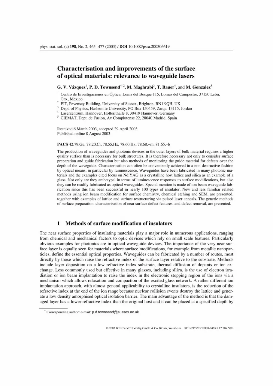
CL measurements have revealed that the Nd line positions and intensities are not stable with time in amorphised surfaces of Nd:YAG. Instabilities might be linked to a loss of oxygen from the surface dur-ing ion implantation, which can be restored by exposure to the atmosphere, but an equally strong possi-bility is uptake of atmospheric water [7, 8]. As mentioned, CL is not a passive surface probe and one must bear in mind that repeated measurements with energetic electron beams may contribute to surface modifications which range from the familiar degradation and colour centre formation in alkali halides [9], densification of silicates [10, 11], to relaxations giving improved crystallinity of LiNbO3 [12] . Whilst depth information is contained in energy dependent data one should note that the electron en-ergy deposition is not uniform with depth, but peaks at about 30% of the average electron range [3, 13]. Intensity values are a function of the depth dependent luminescence efficiency which is sensitive to elec-tron–hole recombination, imperfections, dislocations and exciton diffusion into the bulk region. In order to assess the surface damage caused by cutting and polishing, data are shown in Fig. 1 [3] for three dif-ferent electron energies, (5, 10 and 20 keV) into Nd:YAG in order to probe to different depths below the surface. The figure indicates measurable shifts both in emission wavelengths and relative line intensities implying changing lattice distortions and/or different interactions with imperfections as a function of depth. In the case of Nd:YAG destruction of the long range lattice order, for example by ion beam amor-phisation, results in almost complete loss of cathodoluminescence signal. Even for the large boules produced for laser materials such as Nd:YAG the crystal quality varies across the diameter of the boule. This is reflected in the ease with which different sections of the boule respond to polishing and to the signals obtained from the CL. Again one is able to record the small changes in lattice parameter or interactions with lattice distortions via line shifts of the narrow transition lines of the Nd ions and the Nd line shifts are greater for the poorly polished regions. The trend is that the shorter wavelength lines move to even shorter wavelengths, whereas conversely the lines near 805 nm move slightly to longer transition wavelengths. Depth dependent effects in waveguides are apparent both in crystalline and amorphous insulators and as a glass example one may cite studies of the waveguide layer formed on the surface of float glass by the ingress of tin during the production of the planar glass [3, 14]. There is a large increase in refractive
Fig. 1 Cathodoluminescence spectra from Nd:YAG obtained with three energies showing modified spectra and differences across the boule.
468 G. V. Vázquez et al.: Characterisation and improvements of the surface of optical materials
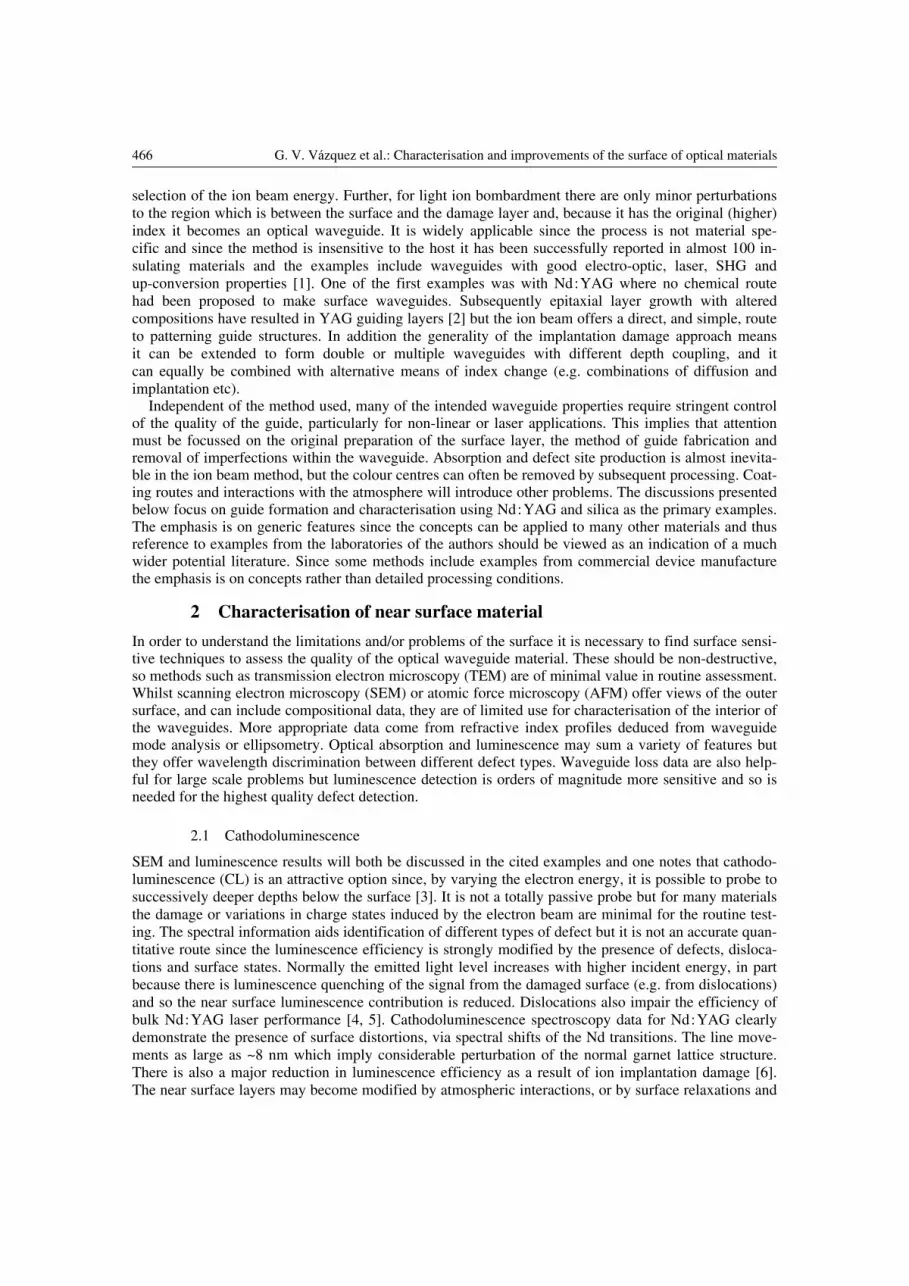
index from the addition of tin which transforms the surface in a vast planar waveguide. Cathodolumines-cence spectra of the glass reveal that the intrinsic defects, the concentration of tin and the charge state of the tin, as well as secondary dopants such as iron, all vary in different ways with depth. There are signals linked to the presence of tin which come from intrinsic silicate defects that are stabilised by the impuri-ties. The CL is therefore a wavelength (and thus defect) selective depth probe of the glass surface. Dis-continuities in signal with depth are matched by discontinuities in the refractive index profile of the waveguide. Figure 2 indicates how CL and index profiles compare in these alternative routes to depth analysis.
2.2 Scanning electron microscopy and surface chemistry
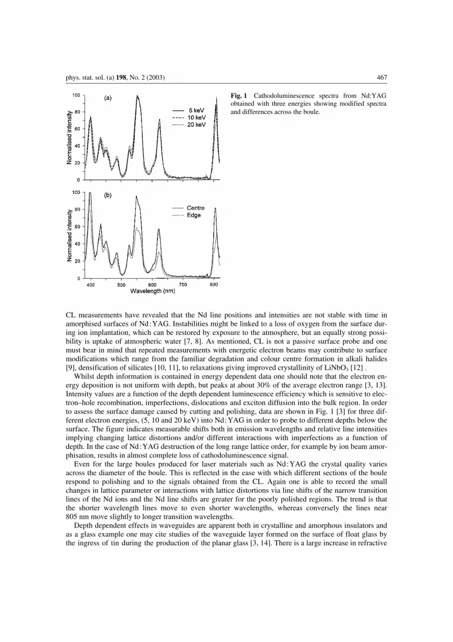
Scanning electron microscopy (SEM) offers images of the immediate surface structure and some infor-mation on the existence of phases and dislocations. In practice the imaging tends to concentrate on areas which contain these surface features, even though they may represent a small percentage of the surface. For waveguide type applications the technique does not directly reveal the quality of the subsurface layer which defines the waveguide. In order to reveal this material a destructive approach such as chemical etching is required. Chemical attack preferentially occurs at the emergent surface dislocations and so can indicate the dislocation density. Further, the surface preparation steps of cutting and polishing of optical materials has historically aimed at a flat and featureless surface appearance. Unfortunately for waveguide type applications this is not an optimal criterion since the outer layer may be prepared with a sequence of large and progressively smaller polishing grits which leave a flat outer layer but do so having introduced strains and buried dislocations to depth of several microns (i.e. at least comparable with the grain sizes of the largest polishing grits). Figure 3 shows that the apparently featureless surface layer of a well polished Nd:YAG crystal can disguise a high density of buried polishing grit induced features [6]. In this example the etching indicates that conventional polishing is responsible both for more than 105/cm2 emergent dislocations and a dense network of “scratch” lines hidden beneath the surface. As will be mentioned below, such problems can be minimised by ion beam amorphisation of the surface layer.
Fig. 2 Comparison of the refractive index depth profiles produced by tin in the surface of float glass compared with the Sn signals seen by Rutherford Back-scattering spectroscopy, and the cathodo-luminescence signals recorded at 1.97 and 2.68 eV. The RBS and CL data required polishing to section different layers.

phys. stat. sol. (a) 198, No. 2 (2003) 469
The surface damage and dislocations are clearly more serious for waveguide structures since even the lower bulk dislocation densities influence Nd:YAG laser rod performance. The threshold power corre-lates with the dislocation density and a factor of 102 reduction in dislocation density can reduce the lasing threshold power by a factor of two [4, 5]. The role of dislocations on the efficiency of second harmonic generation (SHG) from the surface of Nd:YAG is equally noticeable [15]. In comparisons between a sample for which SHG was recorded after polishing the signal was then used to monitor changes during a sequence of amorphisation and chemical etching to expose a new surface with a re-duced dislocation density. Amorphisation reduced the signal to just 5% of the initial value but the new crystalline surface, which was exposed after the etching, gave higher SHG than the initial value by some 24% [16].
2.3 Related polishing and chemical effects
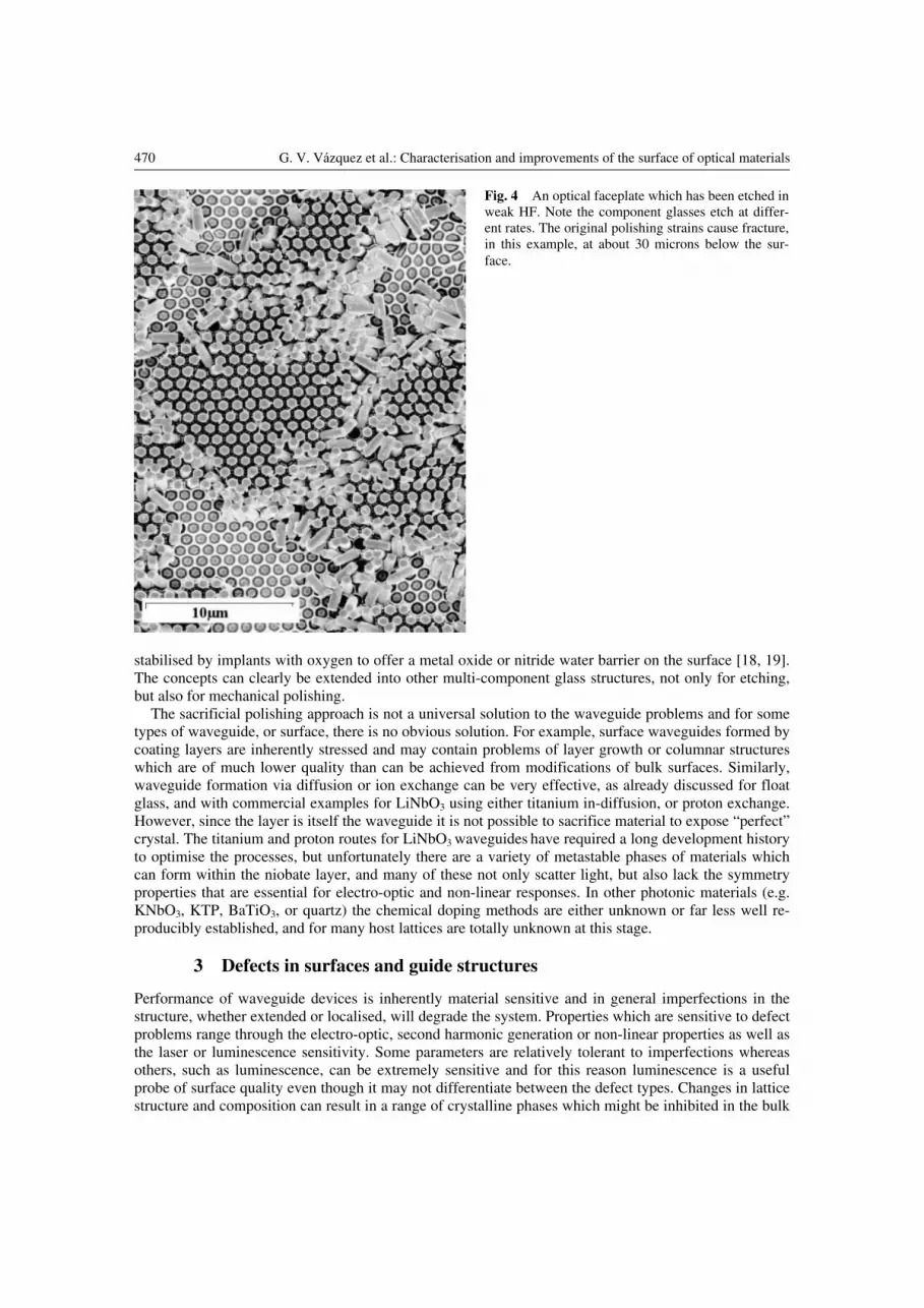
Similar problems of surface preparation exist for semiconductor technology but in that discipline there is acceptance of the need to lose quite large quantities of material in a sacrificial manner to reach disloca-tion free layers. This is not yet common practice in optics, and definitively not on the depth scale which is required. Polishing damage can extend much greater in depth than is relevant for waveguides. One such long range example occurs for fibre optic faceplates used for photon imaging detectors. Here a severe problem occurs because it is a multi-component glass structure. The mechanical properties of the different glasses cause significant stress and flexure which results in deep layer damage to the fibre bun-dle array. Normal polishing produces a standard flat appearance, but in subsequent chemical etching studies it was revealed that the flat outer surface disguises major stress problems that lead to fracture at depths of up to 100 microns below the surface [17]. Figure 4 shows an example of fibre fragments which were released from conventionally polished faceplates. To overcome this difficulty it is necessary to use a deep sacrificial layer of several hundred microns in a series of polishing steps with successively finer grits and reduced hardness. This more cautious surface preparation overcomes the problems and greatly improved quality is seen in which etching does not revealed any buried fracture damage. Separation of component glasses has been a requirement during fabrication of devices from a multi-component matrix. In the example of the fibre-optic faceplates there are three types of glass and a variety of interface compositions. Chemically it is not always possible to achieve the desired selectivity with a sufficiently large difference in reaction rates. In order to modify the chemical responses the glass face-plates were ion beam implanted and this changed the relative etch rates. In this particular example [17] an inert implant ion was used but in principle chemically active ions can be selected to enhance or sup-press the surface reactivity [1]. For example the surface of the hygroscopic ZBLAN fluoride glass can be
Fig. 3 The figure shows an original polished Nd:YAG surface (upper section) and the buried polishing induced scratch features which were revealed by ion im-plantation prior to chemical etching (lower section).
470 G. V. Vázquez et al.: Characterisation and improvements of the surface of optical materials
stabilised by implants with oxygen to offer a metal oxide or nitride water barrier on the surface [18, 19]. The concepts can clearly be extended into other multi-component glass structures, not only for etching, but also for mechanical polishing. The sacrificial polishing approach is not a universal solution to the waveguide problems and for some types of waveguide, or surface, there is no obvious solution. For example, surface waveguides formed by coating layers are inherently stressed and may contain problems of layer growth or columnar structures which are of much lower quality than can be achieved from modifications of bulk surfaces. Similarly, waveguide formation via diffusion or ion exchange can be very effective, as already discussed for float glass, and with commercial examples for LiNbO3 using either titanium in-diffusion, or proton exchange. However, since the layer is itself the waveguide it is not possible to sacrifice material to expose “perfect” crystal. The titanium and proton routes for LiNbO3 waveguides have required a long development history to optimise the processes, but unfortunately there are a variety of metastable phases of materials which can form within the niobate layer, and many of these not only scatter light, but also lack the symmetry properties that are essential for electro-optic and non-linear responses. In other photonic materials (e.g. KNbO3, KTP, BaTiO3, or quartz) the chemical doping methods are either unknown or far less well re-producibly established, and for many host lattices are totally unknown at this stage.
3 Defects in surfaces and guide structures
Performance of waveguide devices is inherently material sensitive and in general imperfections in the structure, whether extended or localised, will degrade the system. Properties which are sensitive to defect problems range through the electro-optic, second harmonic generation or non-linear properties as well as the laser or luminescence sensitivity. Some parameters are relatively tolerant to imperfections whereas others, such as luminescence, can be extremely sensitive and for this reason luminescence is a useful probe of surface quality even though it may not differentiate between the defect types. Changes in lattice structure and composition can result in a range of crystalline phases which might be inhibited in the bulk
Fig. 4 An optical faceplate which has been etched in weak HF. Note the component glasses etch at differ-ent rates. The original polishing strains cause fracture, in this example, at about 30 microns below the sur-face.
phys. stat. sol. (a) 198, No. 2 (2003) 471
material. Lithium niobate is a classic example since it contains a range of minor structural phase varia-tions linked to the composition. The most familiar are the congruent (approximately Li0.486Nb0.514O3) and stoichiometric (~LiNbO3) variants, but many other compositions have been documented [20, 21], even in the bulk crystals. The presence of these variants can be expressed through changes in luminescence spec-tra or the optical absorption. For lithium niobate, with dopants of Mg and Ti, there is luminescence evi-dence [22] for small changes in time dependence of the boule growth which shift the stoichiometry and the relative concentrations of the dopants. Separation of effects is possible since the luminescence has characteristic features for each impurity as well as the intrinsic stoichiometry. An important role of lith-ium niobate is in periodically poled structures for SHG production. Recent data show the luminescence efficiency of the strained region of the domain walls between the two poling directions is greatly reduced [23]. The luminescence quenching extends over a width of about a micron, which by implication, sug-gests the domain wall is on this size scale and this is broadly in agreement with data from other tech-niques [24, 25].
4 Evidence for impurity inclusions
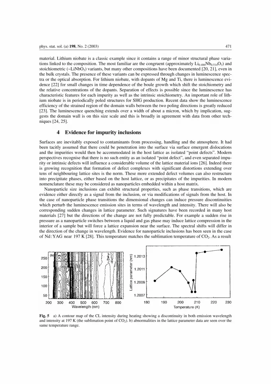
Surfaces are inevitably exposed to contaminants from processing, handling and the atmosphere. It had been tacitly assumed that there could be penetration into the surface via surface emergent dislocations and the impurities would then be accommodated in the host lattice as isolated “point defects”. Modern perspectives recognise that there is no such entity as an isolated “point defect”, and even separated impu-rity or intrinsic defects will influence a considerable volume of the lattice material ions [26]. Indeed there is growing recognition that formation of defect complexes with significant distortions extending over tens of neighbouring lattice sites is the norm. These more extended defect volumes can also restructure into precipitate phases, either based on the host lattice, or as precipitates of the impurities. In modern nomenclature these may be considered as nanoparticles embedded within a host matrix. Nanoparticle size inclusions can exhibit structural properties, such as phase transitions, which are evidence either directly as a signal from the inclusion, or via modifications of signals from the host. In the case of nanoparticle phase transitions the dimensional changes can induce pressure discontinuities which perturb the luminescence emission sites in terms of wavelength and intensity. There will also be corresponding sudden changes in lattice parameter. Such signatures have been recorded in many host materials [27] but the directions of the change are not fully predictable. For example a sudden rise in pressure as a nanoparticle switches between a liquid and gas phase may induce lattice compression in the interior of a sample but will force a lattice expansion near the surface. The spectral shifts will differ in the direction of the change in wavelength. Evidence for nanoparticle inclusions has been seen in the case of Nd:YAG near 197 K [28]. This temperature matches the sublimation temperature of CO2. As a result
Fig. 5 a) A contour map of the CL intensity during heating showing a discontinuity in both emission wavelength and intensity at 197 K (the sublimation point of CO2). b) abnormalities in the lattice parameter data are seen over the same temperature range.

472 G. V. Vázquez et al.: Characterisation and improvements of the surface of optical materials
Fig. 6 An isometric plot of CL during heating for Nd:YAG where the intensity step at 170 K is appar-ent. This corresponds to a phase transition of surface absorbed water which is influencing the lumines-cence intensity.
of this sublimation the volume expansion causes the Nd emission lines originating in the surface layer to undergo a discontinuity in the wavelength of the emission and there is a corresponding anomaly in the lattice parameter data which underwent a step in cell dimension, but remained cubic. Data are shown in Fig. 5. Many other crystalline hosts show almost identical behaviour with equally strong evidence for trapped nanoparticles of other common impurities such as N2 and O2 [27]. An extremely prevalent source of surface contamination that penetrates into the stressed surface layer is water vapour. Numerous luminescence examples have indicated that not only does water enter into the surface to depths on the scale of a micron, but a fraction of it behaves as though it is a bulk material, and even exhibits the phase transitions of ice at low temperatures [8]. These water nanoparticle inclu-sions strongly modify the luminescence efficiency and Nd:YAG offers a particularly clear example of such an effect for the hexagonal to cubic ice transition at 170 K. Figure 6 shows almost com- plete suppression of the CL signals when the ice is in the lower temperature phase. The mechanism for changing the luminescence efficiency is unclear but it is definitely effective over a relatively long range (i.e. ~ micron) and may be a combination of pressure effects and altered dielectric constants. Ice on the surface has a phase change in the vacuum systems near 230 K and this can also be detected in some examples. Whilst the presence of the nanoparticle inclusions, particularly water, is readily seen from the low temperature luminescence data it is probable that they are equally important in many other types of measurement. Since they are dominant in surface effects their influence on waveguide and surface photonics should be carefully considered in future studies.
5 Methods of defect removal
5.1 Amorphisation and chemical etching
An obvious first step to improved surface quality is to demand that the surface preparation and polishing methods generate fewer defects, in particular fewer dislocations. Direct chemical etching of the bulk crystal is much slower than the preferential attack at the dislocation lines (i.e. there is an enhanced etch-ing rate at the dislocations compared to the flat surface resulting from different chemical bond compen-
phys. stat. sol. (a) 198, No. 2 (2003) 473
sation). Whilst useful as a tool in identifying the dislocation density the etching leaves a pitted surface on the original polished and flat surface. Nevertheless, one method which has proved effective with Nd:YAG is to capitalise on the effect that ion beam implantation can amorphise a crystalline layer and hence destroy the original dislocation network. Furthermore, the chemical reactivity of amorphised gar-nets is greatly enhanced [29]. Thus, after the initial polishing, to give the optically flat surface, the layer is ion beam amorphised and then etched. The result is an exposed new surface layer which retains the original flatness and shows no evidence of preferential dislocation etching. Ion beam penetration was chosen to reach a depth of more than a micron below the layer of damage from polishing. An example with Nd:YAG resulted in a change of dislocation density from ~105/cm2 down to ~102/cm2. At the same time the new surface generated cathodoluminescence intensity from the latter surface which was im-proved by 250%. The method of ion beam enhanced etching has been applied to several materials such as LiNbO3, LiTaO3 as well as garnets, and in these examples the etching rate enhancement is between 500 and 1000 times. For amorphised crystalline quartz, which resembles a high density version of silica, it is a factor of 200; and even for amorphous glass the changes in rate are often factors of 3 or more. In each of these examples the main benefit is a new surface with surface flatness, which is comparable, or better than the original optical surface. The progress of the etching through the amorphisation can be followed via CL which, at least for garnets, is strongly suppressed by the amorphisation, but line intensity and wavelength changes indicate the approach of the layer to that characteristic of bulk material. The latter can often be determined by X-ray excitation (radioluminescence, RL).
Not annealed Thermal annealed
Fig. 8 Typical surface structures formed on silica glass by excimer laser pulses. The left figure shows a normal irregular patterning whereas annealing of the silica to remove polishing strains results in a smoother more uniform structure (right hand image).
Fig. 7 Photoluminescence data for bulk and He ion implanted Nd:YAG waveguides. In this example the material had been annealed at 450 oC.

474 G. V. Vázquez et al.: Characterisation and improvements of the surface of optical materials
5.2 Thermal processing
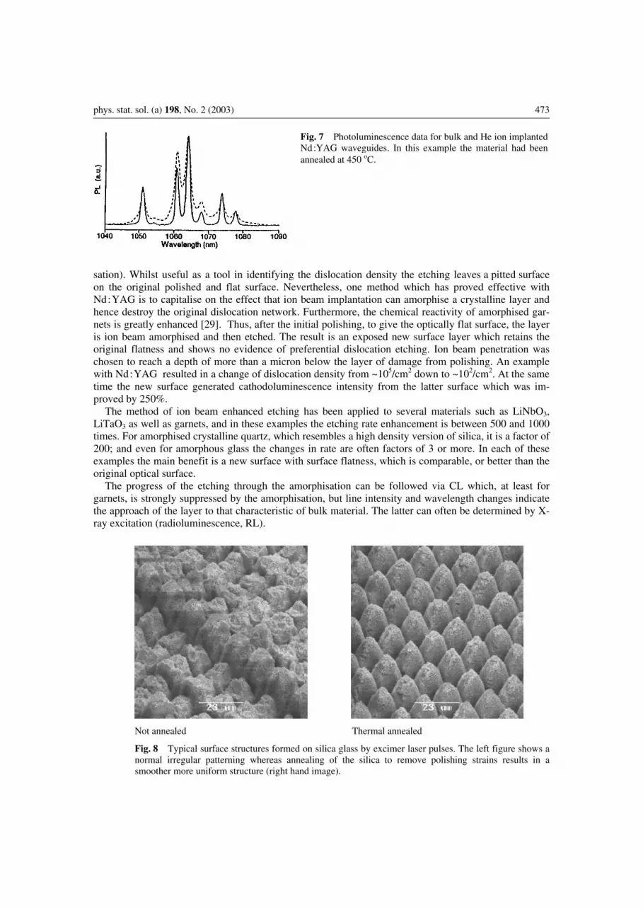
Defect removal can often be considered by high temperature thermal treatments. In many insulators the isolated or small defect complexes can be destroyed at temperatures as low as 200 to 400 oC. Lar- ger defects and dislocations are more troublesome and removal often requires heating to near the melting temperature. High temperature treatments after polishing, and prior to waveguide fabri- cation, may thus be helpful in removing polishing damage. However, thermal processing is not a uni- versal success as high temperature defect formation can occur and some defects will be retained, parti- cularly if the sample is rapidly cooled. Furnace annealing after ion implantation or diffusion dop- ing will similarly have mixed success rates as it may introduce further diffusion of index enhancing dopants, or allow aggregation of impurities. The latter example is clearly a problem where non- linear properties are achieved via the presence of metallic nanoparticle dopants, since changes in par- ticle size give different responses. Temperature selection is also important in ion implanted damage barrier waveguides as one must achieve removal of the absorption losses, without removal of the bar- rier. Several improvement techniques can be combined and for example with Nd:YAG it is necessary to remove some of the helium implant damage within the waveguide layer and this is effective with furnace anneals at say 450 °C. The guide is still structurally different from bulk material as can be seen in Fig. 7 which contrast the photoluminescence of bulk and ion implanted waveguides of the Nd:YAG. [7]. One sees that within the guide the line widths have increased and the two main lines are more equal in inten-sity compared with the spectrum of the bulk material. Similar differences are seen in other spectral re-gions. There are minimal differences in spectral line shapes between the photoluminescence spectra of a normal polished waveguide and one which had been chemically etched to remove surface dislocations prior to the implant. However, the removal of dislocations gives significant changes in photolumines-cence intensity, as well as variations between TE and TM polarisations. In this example the efficiency was raised by up to 40% for the TM polarised signals [7]. In the case of rare earth ions implanted for usage as lasers the damage annealing may result in associa-tion of the dopants since the implant produces a layer which is not in thermodynamic equilibrium. In-deed, precipitate phases are common in heavily doped or damaged material, not only from additives during implantation or diffusion, but even in natural material growth [30, 31] and such precipitates inevi-tably degrade any waveguides. Original surface preparation damage may be manifest in many other applications. To cite a less famil-iar example [32] Fig. 8a shows SEM images of structures which were formed on the surface of silica by laser ablation. The objective here was to write patterned surfaces but the quality of the surface finish is poor and strongly dependent on the initial state of the surface preparation. The images suggest that for a glass layer, as well as for crystalline material, standard polishing methods leave a wealth of sub-surface damage, even though optically the layer has an apparent high degree of flatness and uniformity. Laser patterning of such material then results in a poorly controlled structure. To resolve the problem a furnace annealing stage was introduced between polishing and laser ablation. This allows relaxation to a more uniform and unstressed surface, giving consequent improvement in the laser patterned structure, as shown in Fig. 8b. The figures contrast images from identical laser machining conditions on convention-ally polished and subsequently annealed silica. Additional improvements in the control of laser ablation of insulators, such as silica or sapphire are potentially offered by the use of ion beam implantation damage to generate absorbing colour centres in the layer that is to be patterned. For such wide energy gap materials there is minimal ab- sorption from pulsed excimer laser beams (e.g. from argon or krypton fluoride) and so the power levels need to be high. This encourages charge explosion which can result in fragmentation and surface cracking. In this situation the colour centre absorption caused by helium ion beam damage is beneficial since it both creates absorbing colour centres and introduces a higher conductivity in the surface layer. In an example with silica implanted with helium ions the damaged surface show- ed a threefold fall in the threshold ablation power, and the electrical surface discharges were inhibited [33].
phys. stat. sol. (a) 198, No. 2 (2003) 475
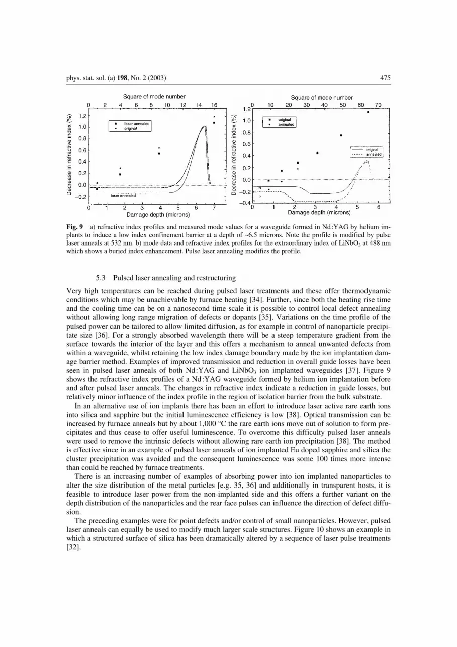
Fig. 9 a) refractive index profiles and measured mode values for a waveguide formed in Nd:YAG by helium im-plants to induce a low index confinement barrier at a depth of ~6.5 microns. Note the profile is modified by pulse laser anneals at 532 nm. b) mode data and refractive index profiles for the extraordinary index of LiNbO3 at 488 nm which shows a buried index enhancement. Pulse laser annealing modifies the profile.
5.3 Pulsed laser annealing and restructuring
Very high temperatures can be reached during pulsed laser treatments and these offer thermodynamic conditions which may be unachievable by furnace heating [34]. Further, since both the heating rise time and the cooling time can be on a nanosecond time scale it is possible to control local defect annealing without allowing long range migration of defects or dopants [35]. Variations on the time profile of the pulsed power can be tailored to allow limited diffusion, as for example in control of nanoparticle precipi-tate size [36]. For a strongly absorbed wavelength there will be a steep temperature gradient from the surface towards the interior of the layer and this offers a mechanism to anneal unwanted defects from within a waveguide, whilst retaining the low index damage boundary made by the ion implantation dam-age barrier method. Examples of improved transmission and reduction in overall guide losses have been seen in pulsed laser anneals of both Nd:YAG and LiNbO3 ion implanted waveguides [37]. Figure 9 shows the refractive index profiles of a Nd:YAG waveguide formed by helium ion implantation before and after pulsed laser anneals. The changes in refractive index indicate a reduction in guide losses, but relatively minor influence of the index profile in the region of isolation barrier from the bulk substrate. In an alternative use of ion implants there has been an effort to introduce laser active rare earth ions into silica and sapphire but the initial luminescence efficiency is low [38]. Optical transmission can be increased by furnace anneals but by about 1,000 °C the rare earth ions move out of solution to form pre-cipitates and thus cease to offer useful luminescence. To overcome this difficulty pulsed laser anneals were used to remove the intrinsic defects without allowing rare earth ion precipitation [38]. The method is effective since in an example of pulsed laser anneals of ion implanted Eu doped sapphire and silica the cluster precipitation was avoided and the consequent luminescence was some 100 times more intense than could be reached by furnace treatments. There is an increasing number of examples of absorbing power into ion implanted nanoparticles to alter the size distribution of the metal particles [e.g. 35, 36] and additionally in transparent hosts, it is feasible to introduce laser power from the non-implanted side and this offers a further variant on the depth distribution of the nanoparticles and the rear face pulses can influence the direction of defect diffu-sion. The preceding examples were for point defects and/or control of small nanoparticles. However, pulsed laser anneals can equally be used to modify much larger scale structures. Figure 10 shows an example in which a structured surface of silica has been dramatically altered by a sequence of laser pulse treatments [32].

476 G. V. Vázquez et al.: Characterisation and improvements of the surface of optical materials
Fig. 10 The left figure shows laser ablated patterns on a silicate glass structure. The right hand image shows the material after a high temperature laser pulse anneal in which the glass has flowed into a com-pletely new structure with the same periodicity.
6 Conclusions
The primary objective of this review was to include highlights of less familiar examples of surface processing with ion beams and to show that many surface related properties can be monitored by surface sensitive luminescence. Further, the examples chosen emphasise the role of ion beams in modifying surface chemistry. Reference was made to pulsed laser structuring on surfaces of insulators, and how pulsed laser treatments can be beneficial in controlling and improving surface related properties such as optical waveguides, luminescence and topography. The choice of the Nd:YAG for many of the illustrations benefits from the narrow line spectra which show wavelength dependence as the result of changes in the local crystal field. Also, the material is a familiar bulk laser which has been successfully fabricated into waveguide lasers by ion beam implantation. The optical techniques described here are helpful in monitoring the effects of surface damage resulting from cutting and polishing, as well as the enhancements produced by ion beam amorphisation and chemical etching to improve the quality of the surface. Further improvements have been shown as the result of pulsed laser anneals. Finally, to empha-sise that the methods are much more generally applicable some brief reference to signals from other materials are cited.
Acknowledgements We wish to thank the EPSRC (UK), CONACYT (Mexico) and the EU Framework V (IM-PECABLE contract G5RD-CT-2000-00372 ) for financial support.
References
[1] P. D. Townsend, P. J. Chandler, and L. Zhang, Optical effects of ion implantation, Cambridge University Press, Cambridge, (1994).
[2] B. Ferrand, B. Chambaz, and M. Couchaud, Opt. Mater. 11, 101 (1999). [3] P. D. Townsend, T. Karali, A. P. Rowlands, V. A. Smith, and G. V. Vazquez, Mineralogical Magazine 63,
211–226, (1999). [4] Peizhen Deng and Jingwen Qiao, J. Cryst Growth 82, 579 (1987). [5] Fuxi Gan, Laser Materials, World Scientific, Singapore (1995). [6] A. Peto, P. D. Townsend, D. E. Hole, and S. Harmer, J. Mod. Opt., 44, 1217, (1997). [7] A. P. Rowlands, A. Peto, P. D. Townsend, P. J. Chandler, S. Harmer, D. E. Hole, J. Olivares, and D. P. Ran-
dall, Luminescence Materials VI, Eds. C. R. Ronda and T. Welker (Electrochemical Society, Pennington, USA), 97–29, 165–176, (1998).
[8] K. Kurt, V. Ramachandran, M. Maghrabi, P. D. Townsend, and B. Yang, J. Phys.: Condens. Matter 14, 4319, (2002).
[9] F. Agullo-Lopez, C. R. A. Catlow, and P. D. Townsend, Point Defects in Materials, Academic Press, London (1988).
phys. stat. sol. (a) 198, No. 2 (2003) 477
[10] G. W. Arnold, J. Non-Cryst. Solids 179, 288 (1994). [11] A. J. Houghton and P. D. Townsend, Appl. Phys. Lett. 29, 855 (1976). [12] R. S. Lowther-Harris, S. D. Brown, P. W. Haycock, P. J. Chandler, L. Zhang, C. C. Tang, R. P. Findlay,
L. Babsail, M. Rodman, J. Knight, and P. D. Townsend, Nucl. Instrum. Methods B 97, 337, (1995). [13] B. G. Yacobi and D. B. Holt, Cathodoluminescence microscopy of inorganic solids, Plenum Press, New York,
(1990). [14] P. D. Townsend, N. Can, P. J. Chandler, B. W. Farmery, R. Lopez-Heredero, A. Peto, L. Salvin, D. Under-
down, and B. Yang, J. Non-Cryst. Solids 223, 73–85, (1998). [15] A. K. Jazmati, G. V. Vázquez, and P. D. Townsend, Nucl. Inst. Methods B 166–167, 592, (2000). [16] G. V. Vázquez, J. R. Rams, P. D. Townsend, and D. E. Hole, Opt. Commsun 167, 171, (1999). [17] M. González, P. D. Townsend, G. Gonzalez, and D. E. Hole, J. Phys Chem. Solids, in press (2003). [18] Y. S. Dai, T. Kawaguchi, K. Suzuki, S. Suzuki, and K. Yamamoto, J. Non-Cryst. Solids 142, 159, (1992). [19] Y. Dai, T. Kawaguchi, K. Suzuki, S. Suzuki, K. Yamamoto, and A. Masui, Appl. Phys. Lett. 58, 422, (1991). [20] A. M. Prokhorov and Yu. S. Kuz’minov, Physics and Chemistry of crystalline lithium niobate, Adam Hilger,
Bristol, (1990). [21] M. E. Lines and A. M. Glass, Principles and applications of ferroelectrics and related materials, Clarendon,
Oxford (1977). [22] A. Al-Ghamdi, G. Jones, B. J. Luff, P. D. Townsend, and K. Polgar, Nucl. Instrum. Methods B 32, 51, (1988). [23] R. Brooks, P. D. Townsend, D. E. Hole, D. Callejo, V. Bermudez, and E. Dieguez, J. Phys D, Appl. Phys. 36,
(2003) in press. [24] R. W. Eason (Southampton University) private communication 2002. [25] V. Dierolf, presented at Europhys conf on defects in insulating materials Wroclaw July 2002. [26] P. D. Townsend, A. K. Jazmati, T. Karali, M. Maghrabi, S. G. Raymond, and B. Yang, J. Phys., Condens.
Matter. 13, 2211, (2001), [27] P. D. Townsend, M. Maghrabi, and B. Yang, Nucl. Instrum. Methods B 191, 767, (2002). [28] M. Maghrabi, P. D. Townsend, and G. Vázquez,. J. Phys., Condens. Matter. 13, 2497, (2001). [29] P. J. T. Nunn, J. Olivares, L. Spadoni, P. D. Townsend, D. E. Hole, and B. J. Luff, Nucl. Instrum. Methods B
127/128, 507, (1997). [30] A. Polman, J. Appl. Phys. 82 1, (1997). [31] T. Karali, N. Can, P. D. Townsend, A. P. Rowlands, and J. Hanchar, Am. Mineral. 85, 668, (2000). [32] T. Bauer to be published. [33] S. W. Harmer, D Phil, thesis Sussex, (2000). [34] P. D. Townsend and J. Olivares, Appl. Surf. Sci. 110, 275, (1997). [35] R. A. Wood, P. D. Townsend, N. D. Skelland, D. E. Hole, J. Barton, and C. N. Afonso, J. Appl. Phys. 74,
5754–56, 1993. [36] A. L. Stepanov, D. E. Hole, and P. D. Townsend, Nucl. Instrum. Methods B 166–167, 882, (2000). [37] G. V. Vázquez and P. D. Townsend, Nucl. Instrum. Methods B 191, 110, (2002). [38] N. Can, P. D. Townsend, D. E. Hole, H. V. Snelling, J. M. Ballesteros, and C. N. Afonso, J. Appl. Phys. 78,
6737, (1995).