engineering quantum-dot lasers
TRANSCRIPT

Physica E 8 (2000) 154–163www.elsevier.nl/locate/physe
Engineering quantum-dot lasers
J.H. Marsh ∗, D. Bhattacharyya, A. Saher Helmy, E.A. Avrutin, A.C. Bryce
Department of Electronics and Electrical Engineering, University of Glasgow, Glasgow G12 8QQ, Scotland, UK
Abstract
We discuss recent progress in the engineering of quantum-dot (QD) lasers, focusing on the spectral output, dynamicsand techniques for integration. Two approaches to such engineering are discussed. Firstly, it is suggested that control oflasing spectra in QD lasers is possible by making use of waveguiding-related phenomena (substrate leakage and re ection)which, in unoptimised laser structures, result in the mode grouping e�ect (quasiperiodic spectral modulation). Secondly, �rstexperimental studies of quantum dot intermixing are reported, suggesting that this technique is capable of both improvingthe performance of active QD media and integrating active QD sections with passive waveguides. ? 2000 Elsevier ScienceB.V. All rights reserved.
PACS: 42.55; Px: 68.35; ct: 71.24.+q: 73.20; Dx: 85.30.V
Keywords: III–V semiconductors; Semiconductor lasers; Quantum dots; Interface di�usion
1. Introduction
The predicted advantages of quantum dot (QD)lasers include low-temperature sensitivity of thethreshold current, high modulation frequency andlow chirp [1–3]. Self-organized growth, using theStranski–Krastanow mechanism, is considered to bethe most promising technique for in situ fabrica-tion of quantum dot arrays as a semiconductor lasergain medium [4–6]. Unfortunately, the low con-�nement energies, inhomogeneous broadening dueto dot size uctuations, and factors such as carriertransport delays have so far limited the performance
∗ Corresponding author. Tel.: +44-141-3304790; fax:+44-141-3306002.E-mail address: [email protected] (J.H. Marsh).
of QD lasers, especially at room temperature [7,8].The introduction of vertically coupled QD layers hasimproved the lasing performance at room tempera-ture by increasing the modal gain thus overcomingthe gain saturation e�ect [9,10]. Recently, substan-tial reductions in the threshold-current densities ofquantum-dot (QD) lasers have been achieved [3,11],setting the scene for utilising devices containing QDstructures [11,12]. However, other problems, such asthose related to spectral and dynamic performance,still need to be addressed. Here we discuss recentprogress in the engineering of QD lasers, focusing onthe spectral output, dynamics and techniques for in-tegration. The paper is organised as follows. Section2 deals with speci�c e�ects in quantum-dot lasersrelated to waveguide properties and suggests waysthey can be used to engineer the spectral and dynamic
1386-9477/00/$ - see front matter ? 2000 Elsevier Science B.V. All rights reserved.PII: S 1386 -9477(00)00133 -8

J.H. Marsh et al. / Physica E 8 (2000) 154–163 155
Fig. 1. Plan view (left) and cross-sectional (right) TEM images of vertically stacked InAs=GaAs quantum-dot structure with 4 nm separationlayer thickness.
behaviour of the lasers and to characterise the phys-ical processes in the lasers. Section 3 discusses thetechnique of quantum dot intermixing and its potentialfor monolithic integration of QD lasers as well as forengineering laser performance. Section 4 summarisesthe results and presents general conclusions.
2. Engineering QD laser spectra by adjustingwaveguide parameters
2.1. Lasing spectra: Experimental
The structures used in our work were grown byMOCVD and contained three- and �ve-fold stackedself-organised InAs/InGaAs QD layers [13]; for de-tails of the structures, see Table 1. Plan-view andcross-sectional transmission electron microscope im-ages of three-fold QD samples are shown in Fig. 1.The image in Fig. 1(a) shows a dot density around4× 1010 cm−2 with dots having a lateral size of 15–18 nm. The apparent dot bases are close to beingsquare-shaped, with one side of the bases approxi-mately oriented along 〈1 0 0〉. The dots, however, ap-pear in the TEM image to be slightly elongated alongone of the 〈1 1 0〉 directions. The lasers, fabricatedfrom �ve-fold structures grown under identical condi-tions, were de�ned using photolithography, dry etched
Table 1QD laser structure used in spectral and dynamic studies
Contact layer p+ GaAs 0:6 �mUpper cladding p-Al0:5Ga0:5As 1:0 �mSuperlattice GaAs=Al0:5Ga0:5As 20× (2; 2 nm)Inner cladding GaAs 70 nm3–5 × InAs QDs 1.22 MLStacked QDs Cap layer GaAs 4 nmInner cladding GaAs 70 nmSuperlattice GaAs=Al0:5Ga0:5As 20× (2; 2 nm)Lower cladding n-Al0:5Ga0:5As 1:0 �mBu�er n-GaAs 0:5 �mSubstrate n-GaAs (1 0 0)
to form ridge structures 4 �m wide and 1:45 �m high,and cleaved to lengths between 500 �m and 1.5 mm.Figs. 2–3 show the spectral characteristics of the
1.0 and 1.35 mm long laser samples, respectively.Lasing emission from the 1.0 mm long devices isat �= 1077 nm, and lies on the high-energy side ofthe PL peak (1155 nm at room temperature), indi-cating that excited dot states may be contributingto the room temperature lasing process. The spectracontain several groups of longitudinal modes whichare separated by approximately 2 nm (i.e. about 10intermodal intervals) and are excited one by onewith increasing bias current (in Fig. 2, the groupsare seen as broadened “modes” due to the limitedresolution of the spectrum analyser). Other workers

156 J.H. Marsh et al. / Physica E 8 (2000) 154–163
Fig. 2. Pulsed spectra of 1.0 mm long and 4 �m wide QD ridgewaveguide lasers with increasing bias current at room temperature:I=Ith = 1:04(a), 1.24(b), 1.44(c), 1.65(d).
have reported similar behaviour [14,15]. The spec-tra observed from the longer lasers are signi�cantlydi�erent. Again lasing is shifted slightly towardsshorter wavelengths from the PL maximum (1088nm in this case) but, in addition, a broader structureis centred at an even shorter wavelength (about 1068nm). This second peak has been also observed byother authors [16] and tentatively attributed eitherto transitions from the excited states or to emissionby two groups of dots with di�erent average sizes.
Fig. 3. Pulsed spectra of 1.35 mm long and 4 �m wide QD ridgewaveguide laser with increasing bias current at room temperature:I=Ith = 1:04(a), 1.24(b), 1.44(c), 1.65(d).
An additional modulation with a period (∼ 1:5–2nm) is present in both envelope peaks, similar to,but less pronounced than, that seen from the 1 mmlong sample.
2.2. Lasing spectra: theoretical considerations
We believe the most probable origin of the modegrouping e�ect lies in the waveguide peculiarities ofthe GaAs=InGaAs lasers. The e�ect was �rst reportedfor quantum-well lasers [17] and may be explained as

J.H. Marsh et al. / Physica E 8 (2000) 154–163 157
Fig. 4. Illustration of mode selectivity by substrate leakage andre ection in a laser waveguide.
follows [13,18]. The waveguide transverse mode de-cays exponentially in the semi-in�nite cladding layersof the laser waveguide (Fig. 4). The typical thicknessof a cladding layer in a semiconductor laser, (dc)is ∼ 1–2 �m, (dc = 1 �m in our structure) and issu�ciently wide to form a good waveguide mode,almost identical to that of an ideal waveguide. Never-theless, the waveguide mode has a �nite magnitude,exp(−pdc) at the edge of the cladding layer, where pis the inverse decay length (p ∼ 5 �m−1 in the laserstructure studied here). A small fraction of the modewill then leak out of the cladding, propagating asC exp (iqx) through the transparent substrate ofthickness hs (Fig. 4). Part of this leaking mode isre ected back from the bottom of the substrate,returning towards the cladding with an amplitudeD exp(−iqx), where |D|= r|C|, r being an e�ec-tive re ection coe�cient assigned to the substratebottom [17]. The net loss, ��s, associated withleakage into the substrate is then proportional to|C|2 − |D|2. By assuming continuity of the mode pro-�le and its derivative, Arzhanov et al. [17] showedthat
��s(�) = ��oexp(−2pdc)(1− r2)
1 + r2 − 2r cos( − ’(�)); (1)
where ’(�) = 2qhs + ’0; exp(i ) = (p+ iq)=(p−iq), and ’0 is the e�ective phase shift due to re ec-tion from the substrate bottom. The prefactor, ��0,is of order 1=de� ; de� being the e�ective transversesize of the mode. As de� is typically ∼ 1 �m in aGaAs=AlGaAs laser, this gives ��0 ∼ 104 cm−1.
Fig. 5. Calculated contributions of leakage loss and con�nementfactor modulation to total net gain modulation in a quantum-dotlaser. Top line (solid): total net gain modulation; bottom line(dashed): leakage loss contribution; middle line (dashed–dotted):con�nement modulation.
We see from Eq. (1) that the leakage-related lossis modulated as the substrate path length, ’(�),changes. This results in a modulation in the net modalgain gm(�) ≈ �g−��s − �o, where � is the opti-cal con�nement factor, g is the material gain and�o denotes other losses in the cavity. In addition tothe wavelength-dependent loss term, the substrateleakage and interference result [13,18] in a modu-lation �� = � − �0 of the optical con�nement, �0being the value calculated without leakage. Our nu-merical simulations show that the resulting modalgain modulation ��g (g being the material gain atthreshold) is approximately proportional, and of com-parable magnitude, to �� for a typical structure ofthe type discussed above (Fig. 4). The total modalgain modulation is �gm(�) ≈ ��g−��s; the am-plitude values are of the order of 0:1 cm−1 (Fig. 5)and thus constitute about 1% of the total cavity loss(about 20 cm−1 for the laser structure studied here).As regards the modal gain modulation period ��, iteasily follows from Eqs. (1) that it is inversely pro-portional to the substrate thickness hs: ��= ��=qhs.With the material and waveguide parameters usedin this work, a modulation period of 2–4 nm corre-sponds to a substrate 150–300 �m thick, in agree-ment with what is commonly obtained by substratethinning.Although modal gain modulation due to sub-
strate leakage has been observed in InGaAs=AlGaAs

158 J.H. Marsh et al. / Physica E 8 (2000) 154–163
quantum well lasers, the mode grouping in these lasersis not very pronounced; instead, nearly single-modespectra with some mode hopping have been observed[17]. However, we can expect the e�ect to be moremarked in InGaAs=AlGaAs quantum-dot lasers wherethe lasing spectra are much broader than those typicalin CW operated QW lasers – with or without modegrouping. We believe the reason behind this is a com-bination of a broad gain spectrum, which is due to thestrong inhomogeneous broadening arising from QDsize dispersion, and an increase in gain nonlinearitiesin quantum dots compared to bulk or quantum wellmedia. To investigate this in some more detail, wehave compared the experimentally observed spectrawith those obtained from a multimode rate-equationmodel [13]. The model includes the standard rateequations for carrier (populated dot) density N andintensity of modes Sm (m being the mode number).
dNdt= P − N
�−∑
mgmSm; (2a)
dSm
dt= �
N�+
(�gm − 1
�(m)ph
)Sm; (2b)
where most of the symbols have their standard mean-ing, with P standing for the pumping term (captureminus escape) and the modal photon lifetimes �(m)ph =1=vg�m include the total loss (net gain) modulation asdiscussed above. For the modal gain gm we use thewell-known simple approximation
gm = A(N − Nt)(1− b2m2)(1−∑
k�mkSk
); (3)
where A and Nt are the gain cross-section and thetransparency carrier density, the parameter b.1 is ameasure of the width of the gain spectrum, and thecoe�cients �mk phenomenologically introduce modecoupling due to the fast gain nonlinearities. In prin-ciple, at least two groups of e�ects may be expectedto contribute to these nonlinearities. The �rst e�ectis short-scale spatial hole burning, caused by deple-tion of population inversion at the antinodes of thestanding wave(s) corresponding to the longitudinalmode(s) lasing initially. The second group of e�ectsis related to spectral hole burning, caused by de-pletion of population inversion in those dots whoseelectron–hole level separation is resonant with thelasing mode energy, and related population pulsations
(pulsation-induced four-wave mixing is neglectedbecause mode grouping makes longitudinal modessigni�cantly non-equidistant).It is already known that, for bulk and QW active
media, e�ects associated with both spectral [19] andspatial [20] hole burning are reasonably well describedby an approximate scaling equation of the form
�mk ≈ CA��1 + ����(m− k)
1 + [���(m− k)]2: (4)
Here C is a dimensionless coe�cient that dependson the type of the nonlinearity and the cavity geom-etry; �= vg=2L is the angular frequency separationbetween longitudinal modes (vg being the group ve-locity of light); �− 1 is a numerical parameter related,though not necessarily equal, to the Henry line-widthenhancement factor (�¿ 0 for the case of spectralnonlinearities [19]; �¡ 0 for spatial e�ects, [20]). Fi-nally, �� in Eq. (4) is the nonlinearity relaxation time,i.e. the relaxation time through carrier transport e�ectsof the self-induced grating in the case of the spatiale�ects, or the carrier relaxation time in the case ofspectral e�ects.In the simulations, the parameters (C; �; ��) related
to gain nonlinearities were treated as adjustable pa-rameters. The simulations show that, in the absenceof the quasi-periodic net gain modulation, the e�ectof nonlinearities is to cause the lasing spectrum tobroaden smoothly with increasing pump current. Inthe presence of the net gain modulation, the broad-ening takes the form of an increase in the number ofmode groups involved in lasing (Fig. 6). As seen inFig. 6, we are able to simulate a spectrum similar tothat seen experimentally, the only discrepancy beinga slightly overestimated red shift of the laser spec-trum with current. In the simulation, we assigned thegain nonlinearity a value of �s = CA�� ∼ 10−14 cm3.This is about three orders of magnitude larger thanthe values (10−18–10−17 cm3) typically encounteredin bulk and quantum well materials. Most of thisincrease may be associated, in the light of Eq. (4),with the increased oscillator strength of the opticaltransitions, represented by the gain constant A, inQD active media (A ∼ vg × 10−13 cm2, as opposedto A ∼ vg(10−16–10−15) cm2 in bulk and QW ma-terials). The remaining factor, of the order of sev-eral times to one order of magnitude, we ascribeto the slower nonlinearity relaxation times in QDs.

J.H. Marsh et al. / Physica E 8 (2000) 154–163 159
Fig. 6. Rate-equation simulation of steady-state lasing spectra ina laser with a periodic spectral modulation of the cavity loss.Pumping current I=Ith = 1:05(a), 1.25(b), 1.45(c), 1.65(d).
Localisation of carriers in dots is expected to slowdown the energy relaxation of carriers, hence causingan increase in spectral hole burning and associatednonlinearities, and impede transport e�ects such asdi�usion, hence increasing spatial hole burning [21].However, a positive value of �= 0:7 was used inEq. (4) to reproduce the sign of the lasing spec-trum asymmetry and the red spectral shift of thelasing peak. This implies that the well-developedmultimode regime studied here is likely to be domi-nated by nonlinearities other than spatial hole burn-ing – for example, by spectral hole burning and,possibly, population pulsations. We note, also, thatthe value of �� = 150 fs that we used to �t the exper-imental results was only 2–3 times greater than the
typical values encountered in bulk and quantum wellmedia. This agrees with recent four-wave mixing andpump–probe measurements on QD ampli�ers wherelittle, if any, increase in the characteristic relaxationtimes was observed [22,23]. In other words, e�ects ofcarrier localisation need not be particularly strong tohave a signi�cant e�ect on laser spectra.It has been found [13] that structures with complex
dynamic spectra such as those shown in Fig. 3 alsodisplay complex dynamic behaviour at turn-on, withvery strong relaxation oscillation damping and satel-lite peaks in the relaxation oscillation train. This latterfeature can be explained [13] by postulating slow car-rier exchange between di�erent groups of lasing dotsseparated in space and/or energy. This slow carrierexchange may be due to the same carrier localisatione�ects that slow down carrier relaxation and lead tostrong nonlinearities and result ultimately in the pro-nounced mode grouping.
2.3. Implications for engineering lasing spectra
The experimental and theoretical results above forma consistent picture of the mode grouping e�ect, thusgiving us the con�dence to make some design recom-mendations. For many laser applications, e.g. formode-locked operation, the mode grouping ef-fect is detrimental and needs to be eliminated.Our analysis suggests that this can be achievedby careful optimisation of the waveguide struc-ture, mainly by ensuring that the cladding layersare su�ciently thick. For example, experimen-tally we observed no mode grouping in lasers withcladding layers 1:8 �m thick. Alternatively, con-trol of waveguide selectivity in a QD laser couldbe put to practical use, �rstly as an investigativetool, e.g. to quantify the e�ects of spectral andspatial hole burning in quantum dot lasers and ex-tract relevant parameters, along the lines outlinedabove. A further step would be to use the leak-age and re ection e�ects to engineer the lasingspectra. In a radical design, one could opt for awaveguide structure with a thin cladding, thin sub-strate and smooth lower surface (high re ectance,r) to suppress lasing from all but one group of afew longitudinal modes, or even one single mode.This would eliminate undesired features related tobroad lasing spectra, but at the expense of a further

160 J.H. Marsh et al. / Physica E 8 (2000) 154–163
Table 2QD structure used in intermixing studies
Contact p+ GaAs 0:6 �mGraded p-Al0:3→0 0:1 �mUpper cladding p-Al0:3Ga0:7As 1:2 �mBarrier GaAs 95 nmSingle layer QDs In0:5Ga0:5As 4 MLBarrier GaAs 95 nmLower cladding n-Al0:3Ga0:7As 1:2 �mGraded layer n-Al0→0:3 0:1 �mBu�er n-GaAs 0:3 �mSubstrate n-GaAs (1 0 0)
decrease in the external quantum e�ciency. The mostsatisfactory way to narrow QD laser spectra is, ofcourse, to grow a laser structure with a uniform andnarrow dot size distribution. This is arguably thegreatest challenge presently facing QD laser tech-nology; some of the possibilities of improving thehomogeneity of the size distribution are discussed inthe next section.
3. Quantum-dot intermixing for engineering QDlaser properties
The previous section concentrated on tailoring theproperties of the quantum dot laser waveguide to engi-neer the laser properties; here we concentrate on trim-ming the properties of the active layer. Quantum-dotintermixing appears to be a very promising way toachieve this goal.Initial work on the thermal treatment of QDs was
undertaken recently to investigate the possibilities ofsubsequent growth of high-quality GaAs and AlGaAslayers [24,25]. This work revealed that the 3D con-�nement of QDs could be preserved after annealing,hence suggesting that annealing can be used to givepost-growth control of the band gap of QD struc-tures. However, control of the band gap of laser diodestructures must be selective for useful integration,allowing the integration of active and passive de-vices on the same chip. Techniques originally devel-oped for quantum-well intermixing are investigatedin this section as means of QD intermixing (QDI)[26].The structure used in this work was a p–i–n
separate con�nement heterostructure grown using
Fig. 7. QD band-gap shift as a function of annealing temperaturefor the di�erent samples.
MBE and containing a single layer of self-organisedIn0:5As0:5As=GaAs QDs as shown in Table 2. Two in-termixing techniques were investigated: impurity-freevacancy disordering (IFVD) using PECVD SiO2[26], and irradiation-damage-induced intermixing us-ing sputtered SiO2 [27]. Samples annealed withoutany caps were also used as controls. All samples wereannealed epi-layer down on a fresh piece of GaAs atdi�erent temperatures for 60 s. After etching the topcontact layer and the upper cladding of the structure,PL measurements were carried out at 77 K using anAr+ laser (�= 514 nm).Samples annealed without a cap layer show blue
shifts of up to 77 meV as can be seen in Fig. 7,but the PL line widths were broader than that of theas-grown sample, as can be seen in Fig. 8. Sam-ples annealed with PECVD SiO2 show blue shiftsof up to 228 meV, with a signi�cant narrowingof the PL line width, from 80 meV for as-grownsamples to 27 meV when annealed at 950◦C. In-termixing will modify the strain distribution, andlead to a blue shift due to alloying and a red shiftdue to the decreased quantum con�nement. It ap-pears that, as for strained and unstrained QW struc-tures, the alloying e�ect dominates. The line-widthnarrowing can be explained by assuming that theintermixing increases the geometrical size of dotswhilst preserving the absolute size dispersion, henceleading to a decrease in the relative dispersion andto line-width narrowing. Further experimental and
J.H. Marsh et al. / Physica E 8 (2000) 154–163 161
Fig. 8. QD emission line width as a function of increase in band-gap energy.
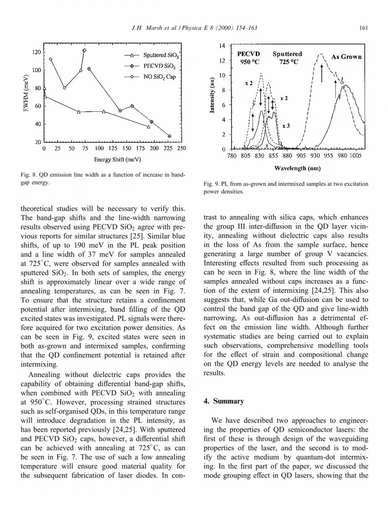
theoretical studies will be necessary to verify this.The band-gap shifts and the line-width narrowingresults observed using PECVD SiO2 agree with pre-vious reports for similar structures [25]. Similar blueshifts, of up to 190 meV in the PL peak positionand a line width of 37 meV for samples annealedat 725◦C, were observed for samples annealed withsputtered SiO2. In both sets of samples, the energyshift is approximately linear over a wide range ofannealing temperatures, as can be seen in Fig. 7.To ensure that the structure retains a con�nementpotential after intermixing, band �lling of the QDexcited states was investigated. PL signals were there-fore acquired for two excitation power densities. Ascan be seen in Fig. 9, excited states were seen inboth as-grown and intermixed samples, con�rmingthat the QD con�nement potential is retained afterintermixing.Annealing without dielectric caps provides the
capability of obtaining di�erential band-gap shifts,when combined with PECVD SiO2 with annealingat 950◦C. However, processing strained structuressuch as self-organised QDs, in this temperature rangewill introduce degradation in the PL intensity, ashas been reported previously [24,25]. With sputteredand PECVD SiO2 caps, however, a di�erential shiftcan be achieved with annealing at 725◦C, as canbe seen in Fig. 7. The use of such a low annealingtemperature will ensure good material quality forthe subsequent fabrication of laser diodes. In con-
Fig. 9. PL from as-grown and intermixed samples at two excitationpower densities.
trast to annealing with silica caps, which enhancesthe group III inter-di�usion in the QD layer vicin-ity, annealing without dielectric caps also resultsin the loss of As from the sample surface, hencegenerating a large number of group V vacancies.Interesting e�ects resulted from such processing ascan be seen in Fig. 8, where the line width of thesamples annealed without caps increases as a func-tion of the extent of intermixing [24,25]. This alsosuggests that, while Ga out-di�usion can be used tocontrol the band gap of the QD and give line-widthnarrowing, As out-di�usion has a detrimental ef-fect on the emission line width. Although furthersystematic studies are being carried out to explainsuch observations, comprehensive modelling toolsfor the e�ect of strain and compositional changeon the QD energy levels are needed to analyse theresults.
4. Summary
We have described two approaches to engineer-ing the properties of QD semiconductor lasers: the�rst of these is through design of the waveguidingproperties of the laser, and the second is to mod-ify the active medium by quantum-dot intermix-ing. In the �rst part of the paper, we discussed themode grouping e�ect in QD lasers, showing that the

162 J.H. Marsh et al. / Physica E 8 (2000) 154–163
origin of the e�ect is leakage of the transverse modethrough the cladding layers followed by re ectionfrom the substrate. This e�ect is purely electro-magnetic and is not restricted to QD lasers, butthe e�ect is signi�cantly increased in QDs throughthe strong optical nonlinearities arising from carrierlocalisation. Possible uses of this e�ect for char-acterisation of laser nonlinearities and trimminglasing spectra have been suggested. In the secondpart of the paper, we demonstrated selective con-trol of the luminescence from QD layers by quan-tum dot intermixing techniques (impurity-free va-cancy disordering and irradiation-damage-inducedintermixing). Substantial (∼ 100meV) di�eren-tial emission peak shifts, su�cient for integrat-ing active and passive waveguides, as well assigni�cant spectral narrowing, have been demon-strated.We conclude by pointing out a certain asymme-
try between the two approaches to QD engineeringdiscussed here. On the one hand, the mode groupingand associated e�ects are now reasonably well under-stood; but the potential of their use for engineeringlaser properties is somewhat limited as discussed inSection 2.3. The studies of quantum-dot intermixing,on the other hand, are at present at a relatively earlystage, with extensive experimental and theoretical in-vestigations needed to achieve a thorough understand-ing of the mechanisms involved. However, prelimi-nary results are encouraging and the prospects verypromising.
Acknowledgements
The authors would like to thank the sta� of the Io�ePhysico-Technical Institute, St. Petersburg, Russia, D.Bimberg and F. Heinrichsdor� of the Technical Uni-versity of Berlin, and A. Onishchenko and E. O’Reillyof the University of Surrey, UK, for useful discus-sions.
References
[1] Y. Arakawa, H. Sakaki, Appl. Phys. Lett. 40 (11) (1982)939–941.
[2] M. Asada, Y. Miyamoto, Y. Suematsu, IEEE J. QuantumElectron. 22 (9) (1986) 1915–1921.
[3] D. Bimberg, N. Kirstaedter, N.N. Ledenstov, Zh.I. Alferov,P.S. Kop’ev, V.M. Ustinov, IEEE J. Selected Topics Quant.Electron. 3 (1997) 196–205.
[4] L. Goldstein, F. Glas, J.Y. Marzin, M.N. Charasse, G. Leroux,Appl. Phys. Lett. 47 (10) (1985) 1099–1101.
[5] D. Leonard, M. Krishnamurthy, C.M. Reaves, S.P. Denbaars,P.M. Petro�, Appl. Phys. Lett. 63 (23) (1993) 3203–3205.
[6] N. Kirstaedter, N.N. Ledentsov, M. Grundmann, D. Bimberg,V.M. Ustinov, S.S. Ruvimov, M.V. Maximov. P.S. Kop’ev,Zh.I. Alferov, U. Richter, P. Werner, U. G�osele, J.Heydenreich, Electron. Lett. 30 (17) (1994) 1416–1417.
[7] D. Klotzkin, K. Kamath, P. Bhattacharya, IEEE Photon.Technol. Lett. 9 (10) (1997) 1301–1303.
[8] H. Benisty, C.M. Sotomayor-Torres, C. Weisbuch, Phys. Rev.B 44 (19) (1991) 10945–10948.
[9] Q. Xie, A. Madhukar, P. Chen, N.P. Kobayashi, Phys. Rev.Lett. 75 (13) (1995) 2542–2545.
[10] O.G. Schmidt, N. Kirstaedter, N.N. Ledentsov, M.H. Mao,D. Bimberg, V.M. Ustinov, A.E. Egorov, A.E. Zhukov, M.V.Maximov, P.S. Kop’ev, Zh.I. Alferov, Electron. Lett. 32 (14)(1996) 1302–1304.
[11] P. Bhattacharya, K. Kamath, J. Singh, D. Klotzkin, J. Phillips,H.-T. Jiang, N. Cheverla, T. Norris, T. Sosnowski, IEEETrans. Electron. Dev. 46 (1999) 871–883.
[12] H. Jiang, J. Singh, IEEE J. Quant. Electron. 34 (1998) 1188–1196.
[13] D. Bhattacharyya, E.A. Avrutin, A.C. Bryce, J.M. Gray, J.H.Marsh, D. Bimberg, F. Heinrichsdor�, V.M. Ustinov, S.V.Zaitsev, N.N. Ledentsov, P.S. Kop’ev, Zh.I. Alferov, A.I.Onishchenko, E.P. O’Reilly, J. Selected Topics QuantumElectron. 5 (1999) 648–657.
[14] N.Yu. Gordeev, A.M. Georgievski, V.I. Kopchatov, S.V.Zaitzev, A.Yu. Egorov, A.R. Kovsh, V.M. Ustinov, A.E.Zhukov, P.S. Kop’ev, Modal composition of radiation inroom-temperature quantum dot lasers, Proceedings of theFifth International Symposium on Nanostructures: Physicsand Technology, St. Petersburg, Russia, 1997, pp. 183–186.
[15] L. Harris, D.J. Mowbray, M.S. Skolnick, M. Hopkinson,G. Hill, Appl. Phys. Lett. 73 (7) (1998) 969–971.
[16] W. Zhou, O. Qasaimeh, J. Philips, S. Krishna, P.Bhattacharya, Appl. Phys. Lett. 74 (6) (1999) 783–785.
[17] E.V. Arzhanov, A.P. Bogatov. V.P. Konyaev, O.M. Nikitina,V.I. Shveikin, Quantum Electron. 24 (7) (1994) 581–587.
[18] E.P. O’Reilly, A.I. Onishchenko, E.A. Avrutin, D.Bhattacharyya, J.H. Marsh, Electron. Lett. 34 (21) (1998)2035–2037.
[19] G.P. Agrawal, IEEE J. Quantum Electron. 23 (6) (1987)860–868.
[20] H.E. Lassen, H. Olesen, B. Tromborg, IEEE Photon. Technol.Lett. 1 (9) (1989) 261–263.
[21] L.V. Asryan, R.A. Suris, Appl. Phys. Lett. 74 (9) (1999)1215–1217.
[22] P. Borri, W. Langbein, J.M. Hvam, Technical Univ. Denmark,Denmark.
[23] M.-H. Mao, F. Heinrichsdor�, D. Bimberg, Ultrafastdynamics in InAs=GaAs quantum dot ampli�ers, Conferenceon Lasers and Electro-Optics (CLEO ’99), Baltimore, 24-29May 1999, paper CWL5.

J.H. Marsh et al. / Physica E 8 (2000) 154–163 163
[24] A.O. Kosogov, P. Werner, U. G�osele, N.N. Ledentsov, D.Bimberg, V.M. Ustinov, A.Yu. Egorov, A.E. Zhukov, P.S.Kop’ev, N.A. Bert, Appl. Phys. Lett. 69 (1996) 3072–3074.
[25] S. Malik, C. Roberts, R. Murray, M. Pate, Appl. Phys. Lett.71 (1997) 1987–1989.
[26] A.C. Bryce, F. Camacho, P. Cusumano, J.H. Marsh, IEEE J.Selected Topics Quant. Electron. 3 (1997) 885–892.
[27] O. Kowalski, C.J. Hamilton, S.D. McDougall, J.H. Marsh,A.C. Bryce, R.M. De La Rue, B. V�ogele, C.R. Stanley, Appl.Phys. Lett. 72 (1998) 581–583.