broadcast console - bitsavers.org
TRANSCRIPT
Broadcast Console
99-1000-1 CU (12-input mainframe, 115 volt supply) 99-1000-1 CUX (230 volt supply)
99-1000-2CU (20-input mainframe, 115 volt supply) 99-1000-2CUX (230 volt vsupply)
Operations &
Technical Manual
PR&E Document 75-40

Broadcast Console
99-1000-1 CU (12-input mainframe, 115 volt supply) 99-1000-1 CUX (12-input mainframe, 230 volt supply)
99-1000-2CU (20-input mainframe, 115 volt supply) 99-1 000-2CUX (20-input mainframe, 230 volt supply)
Operations &
Technical Manual
PR&E 75-40 Revision A • 3/99
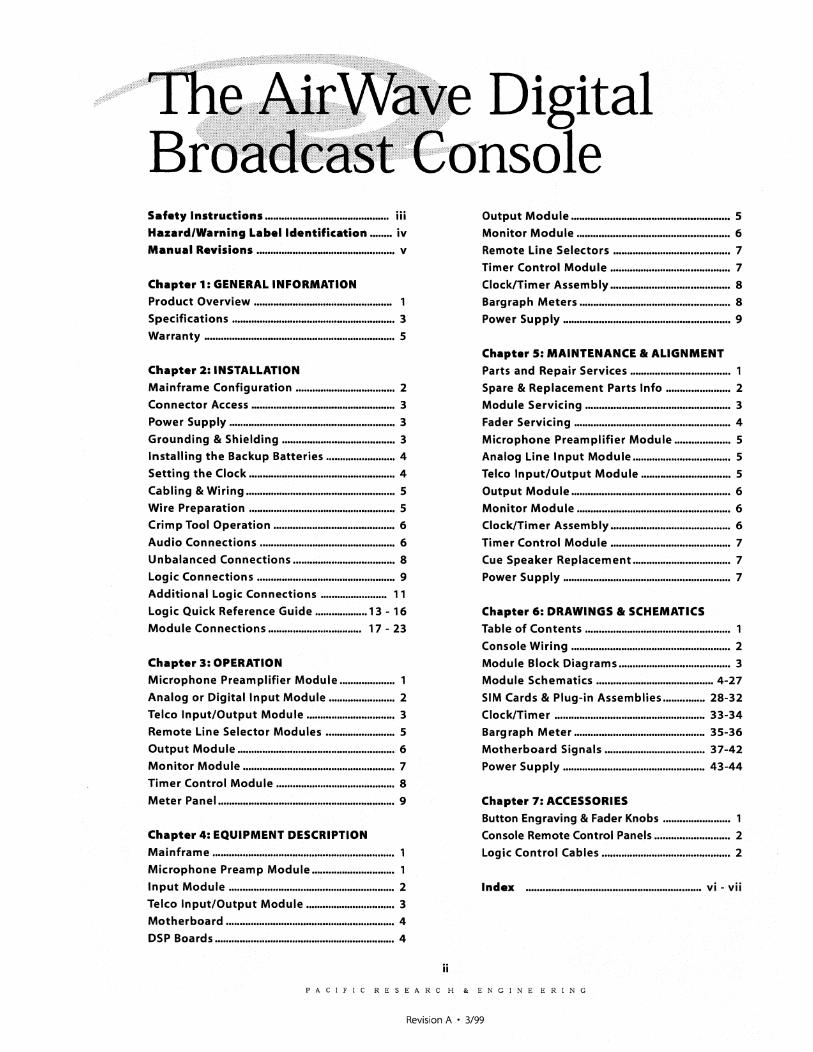
Safety Instructions ............................................. iii
Hazard/Warning Label Identification •••••••• iv
Manual Revisions .................................................. v
Chapter 1: GENERAL INFORMATION
Product Overview ................................................. .
Specifications ........................................................... 3
Warranty ..................................................................... 5
Chapter 2: INSTALLATION
Mainframe Configuration .................................... 2
Connector Access .................................................... 3
Power Supply ............................................................ 3
Grounding It Shielding ......................................... 3
Installing the Backup Batteries ......................... 4
Setting the Clock ..................................................... 4
Cabling It Wiring ...................................................... 5
Wire Preparation ..................................................... 5
Crimp Tool Operation ............................................ 6
Audio Connections ................................................. 6
Unbalanced Connections ..................................... 8
Logic Connections .................................................. 9
Additional Logic Connections ........................ 11
Logic Quick Reference Guide ................... 13 - 16
Module Connections .................................. 17 - 23
Chapter 3: OPERATION
Microphone Preamplifier Module .................... 1
Analog or Digital Input Module ........................ 2
Telco Input/Output Module ................................ 3
Remote Line Selector Modules ......................... 5
Output Module ......................................................... 6
Monitor Module ....................................................... 7
Timer Control Module ........................................... 8
Meter Panel ................................................................ 9
Chapter 4: EQUIPMENT DESCRIPTION
Mainframe .................................................................. 1
Microphone Preamp Module .............................. 1
Input Module ............................................................ 2
Telco Input/Output Module ................................ 3
Motherboard ............................................................. 4
DSP Boards ................................................................. 4
Digital .............. .:::., .... nso 1 e
Output Module ......................................................... 5
Monitor Module ....................................................... 6
Remote Line Selectors .......................................... 7
Timer Control Module ........................................... 7
Clock/Timer Assembly ........................................... 8
Bargraph Meters ...................................................... 8
Power Supply ............................................................ 9
Chapter 5: MAINTENANCE It ALIGNMENT
Parts and Repair Services .................................... 1
Spare It Replacement Parts Info ....................... 2
Module Servicing .................................................... 3
Fader Servicing ........................................................ 4
Microphone Preamplifier Module .................... 5
Analog Line Input Module ................................... 5
Telco Input/Output Module ................................ 5
Output Module ......................................................... 6
Monitor Module ....................................................... 6
Clock/Timer Assembly ........................................... 6
Timer Control Module ........................................... 7
Cue Speaker Replacement ................................... 7
Power Supply ............................................................ 7
Chapter 6: DRAWINGS It SCHEMATICS
Table of Contents .................................................... 1
Console Wiring ......................................................... 2
Module Block Diagrams ........................................ 3
Module Schematics .......................................... 4-27
SIM Cards It Plug-in Assemblies ............... 28-32
Clock/Timer ...................................................... 33-34
Barg raph Meter ............................................... 35-36
Motherboard Signals .................................... 37-42
Power Supply ................................................... 43-44
Chapter 7: ACCESSORIES
Button Engraving It Fader Knobs ........................ 1
Console Remote Control Panels ........................... 2
Logic Control Cables .............................................. 2
Index ............................................................... vi - vii
ii
PACIFIC RESEARCH & ENGINEERING
Revision A • 3/99
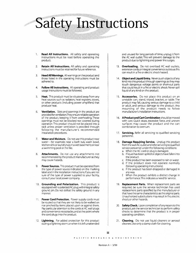
1. Read All Instructions. All safety and operating instructions must be read before operating the product.
2. Retain All Instructions. All safety and operating instructions must be retained for future reference.
3. Heed A1IWamings. All warnings on the product and those listed in the operating instructions must be adhered to.
4. Follow All Instructions. All operating and product usage instructions must be followed.
5. Heat. This product must be situated away from any heat sources such as radiators, heat registers, stoves, or other products (including power amplifiers) that produce heat.
6. Ventilation. Slots and openings in the product are provided forventiiation.They ensure reliable operation of the product, keeping it from overheating. These openings must not be blocked nor covered during operation. This product should not be placed into a rack unless proper ventilation is provided through following the manufacturer's recommended installation procedures.
7. Water and Moisture. Do not use this product near water-for example; near a bath tub, wash bowl, kitchen sinkorlaundrytub;in a wet basement;ornear a swimming pool orthe like.
8. Attachments. Do not use any attachments not recommended by the product manufacturer as they may cause hazards.
9. Power Sources. This product must be operated from the type of power source indicated on the marking label and in the installation instructions. If you are not sure of the type of power supplied to your facility, consult your local power company.
10. Grounding and Polarization. This product is equipped with a polarized AC plug with integral safety ground pin. Do not defeat the safety ground in any manner.
11. Power Cord Protection. Power supply cords must be routed so that they are not likely to be walked on nor pinched by items placed upon or against them. Pay particular attention to the cords at AC wall plugs and convenience receptacles,and atthe point where the cord plugs into the product.
12 Lightning. For added protection for this product during a lightning storm,or when it is left unattended
iii
ctions
and unused for long periods of time, unplug it from the AC wall outlet.This will prevent damage to the product due to lightning and power line surges.
13. Overloading. Do not overload AC wall outlets, extension cords,or integral convenience outlets as this can result in a fire or electric shock hazard.
14. Object and Liquid Entry. Never push objects of any kind into this product through openings as they may touch dangerous voltage points or short-out parts that could result in a fire or electric shock. Never spill liquid of any kind on the product.
15. Accessories. Do not place this product on an unstable cart, stand, tripod, bracket, or table. The product may fall, causing serious damage to a child or adult, and serious damage to the product. Any mounting of the product needs to follow manufacturer's installation instructions.
16. A Product and Cart Combination should be moved with care. Quick stops, excessive force, and uneven surfaces may cause the product and the cart combination to overturn.
17. Servicing. Refer all serviCing to qualified servicing personnel.
18. Damage Requiring Service. Unplug this product from the wall AC outlet and refer servicing to qualified service personnel under the following conditions:
19.
20.
21.
a When the AC cord or plug is damaged. h If liquid has been spilled or objects have fallen into
the product. c Ifthe product has been exposed to rain or water. d If the product does not operate normally
(following operating instructions). e If the product has been dropped or damaged in
anyway. f When the product exhibits a distinct change in
performance.This indicates a need for service.
Replacement Parts. When replacement parts are required, be sure the service technician has used replacement parts specified by the manufacturer or that have the same characteristics as the original parts. Unauthorized substitutions may result in fire,electric shock, or other hazards.
Safety Check. Upon completion of any repairs to this product, ask the service technician to perform safety checks to determine that the product is in proper operating condition.
Cleaning. Do not use liquid cleaners or aerosol cleaners. Use only a damp cloth for cleaning.
PACIFIC RESEARC H & ENGINE ERING
Revision A • 3/99

CAUTION RISK OF ELECTRIC SHOCK
DO NOT OPEN
WARNING: SHOCK HAZARD - DO NOT OPEN AVIS: RISQUE DE CHOC ELECTRIQUE - NE PAS OUVRIR
CAUTION: TO REDUCE THE RISK OF ELECTRIC SHOCK DO NOT REMOVE ANY COVER OR PANEL. NO USER SERVICEABLE PARTS INSIDE. REFER SERVICING TO QUALIFIED SERVICE PERSONNEL.
WARNING: TO REDUCE THE RISK OF FIRE OR ELECTRIC SHOCK, DO NOT EXPOSE THE POWER SUPPLY OR CONSOLE TO RAIN OR MOISTURE.
The Exclamation Point symbol, within an equilateral triangle, alerts the user to the presence of important operating and maintenance (servicing) instructions in product literature and instruction manuals.
The Lightning Flash With Arrowhead symbol, within an equilateral triangle, alerts the user to the presence of uninsulated dangerous voltage within the product's enclosure that may be of sufficient magnitude to constitute a risk of electric shock.
WARNING-This equipment generates, uses and can radiate radio frequency energy. If not installed and used in
accordance with the instructions in this manual it may cause interference to radio communications. It has been tested
and found to comply with the limits for a Class A computing device (pursuant to Subpart J of Part 15 FCC Rules), which
are designed to provide reasonable protection against such interference when operated in a commercial environment.
Operation of this equipment in a residential area is likely to cause interference, in which case the user, at his own ex
pense, will be required to take whatever measures may be required to correct the interference.
iv
PACIFIC RESEARC H & ENGINE ERING
Revision A • 3/99
• SIons
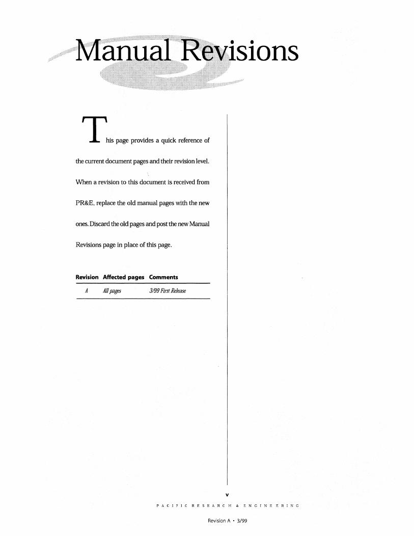
This page pwvides a quick .. ference of
the current document pages and their revision level.
When a revision to this document is received from
PR&E, replace the old manual pages with the new
ones. Discard the old pages and post the new Manual
Revisions page in place of this page.
Revision Affected pages Comments
A AUpages 3/99 First Release
v
PACIFIC RESEARCH & ENGINEERING
Revision A • 3/99
Thanks fo' JoImng the growing rnnks of
broadcasters employing Pacific Research &
Engineering (PR&E) consoles. PR&E supplies
audio products and systems to the world's lead-
ing broadcast facilities. Our mission is to provide
the fmest quality products, systems, documenta-
tion and after-sale support. We invite comments
and suggestions for improvements to this docu-
mentation and to all of our services.
AirWave Digital is a very sophisticated console
with an extensive range of features contained in a
compact design. To obtain maximum benefit from
the console's capabilities, read the InstaJJation, Op
eration and Equipment Description chapters prior to
product installation.
PRODUCT OVERVIEW Each Airwave Digital mainframe ships standard
with one each of these modules:
• Microphone Preamp
• Monitor
• Output i
• Timer Co~trol
The modules are installed into their standard
positions in the mainframe along with the Input
modules ordered. Additional Mic Preamps, Ana-
log or Digital Remote Line Selectors, and up to
two Telco modules, or various accessory panels,
may also be installed per the order. If required,
blank panels are available to cover unused mod
ule positions.
AirWave Digital's motherboard and module area
is completely contained within a welded steel chas
sis for strength and RFI immunity. The meter panel
is hinged at the rear, locking down over the upper
part of each module, covering the audio and logic
connectors and the Logic Settings switches. Be
neath the meter panel, the chassis bottom is open
for easy cable access.
Module Descriptions
Microphone Preamplifier
Contains five preamplifiers with individual gain
controls under a security cover. Phantom power
(+45 VDC) is selectable for each input. The pream
plifier outputs are +4 dBu balanced for connec
tion directly to an Input module or to outboard
mic processing equipment. One module is supplied
standard, but additional Mic Preamplifier mod
ules can be installed into any RLS or input posi
tion.
Input
Each Input module can be configured as an
analog module (with two balanced, stereo inputs),
or as a digital module (with two AES-3 inputs)
through a plug-in SIM (Single In-Line Module).
Each Input module features two input selection
(A or B), channel on/off control, fader level con
trol (with the selectable global fader start feature),
Cue and Off-Line control and output selection to
PACIFIC RESEARC H & ENGINE ERING
Revision A • 3/99
three program buses. Faceplate channel trim con
trols allow the analog version to accept input lev
els from -10 dBu to +4 dBu.
The module's inputs are electronically switched
through a faceplate A/B Input selector. Logic wir
ing to/from external peripherals connects to a 24-
pin logic connector on the faceplate. Logic and
module function options for the A or the B input
are set through a ten-position faceplate DIP switch.
A second, optional interface connector is available
for separate logic control for the A and B inputs.
Telco Input/Output
Up to two optional Telco modules can be in
stalled into the mainframe next to the monitor
module. These provide the audio and logic con
nections for up to two telephone hybrids and two
channel recorders. A faceplate trim control allows
the module to work with hybrid outputs from -10
dBu up to +4 dBu.
EachTelco module's output (Feed to Caller) can
be set manually from between the three program
buses or the Off-Line mix bus. The Autofeed func
tion automatically switches the Feed to Caller be
tween the Off-Line mix and the asSigned Program
bus as the Telco module is turned off and on.
Monitor
A double-width module with the monitoring and
communication controls for a control room (C/R)
and separate studio or voice booth. Volume
controls for C/R and studio speaker volume, C/R
headphone and Cue are included with independent
source selection for each room (three external
inputs, Pgm-1, Pgm-2, Pgm-3 and Telco). The
module includes a C/R to studio talkback system
with built-in adjustable electret talkback mic. Both
C/R and studio warning outputs are provided.
2
Output
.i=t\V."\L=-:;...---i»iGiL'.L'" > 1 Ganaral Information
Contains the various analog stereo line output
amplifiers and the AES-3 digital outputs for the
Program-1 (Pgm-1), Program-2 (Pgm-2) and Pro
gram-3 (Pgm-3) buses. A monaural analog out
put of the Pgm-1, Pgm-2 or Pgm-3 bus (operator
selected) is also provided. Each balanced analog
output uses a nominal level of +4 dBu. Each digi
tal output is AES-3 compatible.
This module also has faceplate buttons for the
right-hand signal level meter selection, Program-
2 or Program-3, with momentary Cue bus level
metering. The module also has two DIP switches
for selecting if Fader Start is enabled and the me
tering scale (VU or PPM) .
Timer Control
Provides manual or automatic control over the
digital timer located in the meter panel. This
module also routes power to the clock/timer
assembly and provides an external reset for a
studio mounted timer. It also provides for a AA
battery backup voltage to hold the console's logic
settings in case of momentary power outage.
Remote Line Selector (RLS)
Two line selectors are available: an analog RLS
and a digital RLS. Each is a 7x2 input selector.
The analog version uses balanced, line-level mono
or stereo Signals. The digital version uses AES-3-
compatible digital signals. Two banks of seven
switches provide manual, exclusive source
selection, among the seven common external input
Signals for the two outputs.
Power Supply
The separately packaged rack mount power
supply is fully regulated and protected by inter
nal fuses and electronic safeguards against exces
sive current.
PACIFIC RESEARC H & ENGINE ERING
Revision A • 3/99
The power supply has five regulated output volt
ages. Two outputs (±16 volts) power the analog
audio circuitry. A third (+5 volts) powers the DSP
and logic control circuitry. The remaining outputs
power the clock/timer assembly (+12 volts) and
supplies phantom powering (+45 volts) for con
denser microphones connected to the Microphone
Preamplifier module.
SPECIFICATIONS AirWave Digital's specifications are significantly
more complete, and the related test conditions
more defined, than those usually shown for con
soles in this class. Be sure to follow the test condi
tions and measure in the units as stated.
The specifications are for a fully-loaded AirWave
Digital-20 mainframe.
Test Conditions: Specifications are for the basic signal paths, per
channel, with 600 ohm loads connected to the
analog program outputs.
o dBu corresponds to an amplitude of 0.775
volts RMS regardless of the circuit impedance. This
is eqUivalent to 0 dBm measured into a 600 ohm
circuit for convenient level measurement with
meters calibrated for 600 ohm circuits.
Noise specifications are based upon a 22 kHz
measurement bandwidth. The use of a meter with
30 kHz bandwidth will result in a noise measure
ment increase of approximately 1. 7 dB.
Total Harmonic Distortion (THD) is measured
at a +23.5 dBu output level using a swept signal
with a 22 kHz low pass filter.
FSD = Full Scale Digital, +24 dBu
Microphone Preamplifiers
Source Impedance: 150 ohms
Input Impedance: 5 k ohms minimum, balanced
Input Level Range: Adjustable, -70 to -30 dEu
Input Headroom: >20 dB above nominal input
3
1 Generel Information
Output Source Impedance: 220 ohms balanced
Nominal Output Level: +4 dBu, balanced
Output Load Impedance: 2.5 k ohms minimum
Analog Line Inputs
Source Impedance: 600 ohms or less
Input Impedance: >40 k ohms, balanced
Input Level Range: Adjustable, -10 to +4 dBu
Input Headroom: 20 dB above nominal input
Analog Main Outputs
Output Source Impedance: 80 ohms balanced
Output Load Impedance: 600 ohms minimum
Nominal Output Levels:
ProgramlMonaural Outputs: adj. +4 dEu
Telephone Mix-Minus: set at +4 dBu
Telephone Recorder Mix Feed: +4 dBu
Maximum Output Levels:
Program and Monaural: +24 dEu
Telco Mix-Minus: +24 dBu
Telco Recorder Mix Feed: +24 dEu
Digital Inputs & Outputs
Reference Level: +4 dBu (-20 dB FSD)
Digital IIO:Thru digital Input or RLS modules
and the digital program outputs.
Signal Format: AES-3, S/PDIF (input only)
AES-3 Input Compliance: 24-bit
AES-3 Output Compliance: 24-bit
Digital Reference Frequency: Internal crystal
Internal Sample Rate: 48 kHz
Processing Resolution: 24-bit fixed with
extended precision accumulators
Conversions: A/D 18-bit Delta-Sigma, 128x
Sample rate conversion on all digital inputs;
D/ A 24-bit, using I-bit conversion
Latency: <1 ms, Mic in to Monitor out; <300 }.Is
digital input to digital output
PACIFIC RESEARCH & ENGINEERING
Revision A • 3/99
Monitor Outputs
Output Source Impedance: 400 ohms, balanced
Output Load Impedance: 2.5 k ohms or greater
Output Level: +4 dBu nominal, +24 dBu max.
Console Headphone Output: 0 dBu, >8 ohm load
External Headphone Amplifier Output:
Source Impedance: 400 ohms
Load Impedance: 2.5 k ohms or greater
Output Level: +4 dEu nominal, +22 dEu max.
Frequency Response
Microphone or Line Input to Program Output:
+0 dB/-0.5 dB, 20 Hz to 20 kHz
Telco Input to Program Output:
+0 dB/-2.0 dB, 20 Hz to 20 kHz
Dynamic Range
Analog Input to Analog Output:
89 dB ref. to FSD, 91 dB "A" weighted to FSD
Digital Input to Analog Output:
92 dB ref. to FSD, 95 dB "A" weighted to FSD
Equivalent Input Noise
Microphone Preamp: -127 dBu, 150 ohm source
Total Harmonic Distortion + Noise
Mic Pre Input to Mic Pre Output: <0.005%, 20 Hz
to 20 kHz, -38 dEu input, + 18 dEu output, 100 k
ohm load, 22 kHz filter bandwidth.
Analog Input to Analog Output: <0.02% at 1kHz,
+ 18 dEu input, + 18 dEu output, 600 ohm load,
22 kHz filter bandwidth.
<0.05%,20 Hz to 20 kHz, +18 dBu input, +18
dBu output, 600 ohm load, 22 kHz filter
bandwidth.
Digital Input to Digital Output: <0.0016%, 20 Hz
to 20 kHz, +18 dEu input, +18 dBu output,
20 kHz fIlter bandwidth
4
1 General Infarmatolan
Digital Input to Analog Output: <0.005% at
1 kHz, + 18 dEu input, + 18 dEu output, 600
ohm load, 22 kHz filter bandwidth.
<0.05%,20 Hz to 20 kHz, +18 dBu input,
+ 18 dEu output, 600 ohm load, 22 kHz filter.
Crosstalk Isolation
Program-to-Program: >90 dB, 20 Hz - 20 kHz
A Input to B Input: >83 dB, 20 Hz - 20 kHz
B Input to A Input: >86 dB, 20 Hz - 20 kHz
Stereo Separation
Analog Program Outputs: >87 dB @ 1 kHz,
>78 dB, 20 Hz to 20 kHz
Console Power Requirements
Fully configured AirWave Digital-12: 120 watts at
115VAC, ±8%, 50/60 Hz
Fully configured AirWave Digital-20: 170 watts at
115VAC, ±8%, 50/60 Hz
Power Supply Main fuse rating: 1.25 amp at 230
VAC (lEC), 2.25 amps at 115VAC (UL)
Power Supply Voltages
Phantom power: +45 VDC at 0.100 Amp
Audio power: ± 16 VDC at 1.00 Amp (each leg)
Digital & Logic power: +5 VDC at 6.5 Amps
and + 12 VDC at 4.0 Amps
Power Supply Ground
Chassis grounded through AC cord.
DC voltages floating from chassis.
Power Supply Connection
AC input: IEC power cord
DC output: Keyed multi-pin connector
Pacific Research & Engineering Corporation
reserves the right to change specifications with
out notice or obligation.
PACIFIC RESEARC H & ENGINE ERING
Revision A • 3/99
WARRANTY The AirWave Digital console carries a
manufacturer's warranty which is subject to the
following gUidelines and limitations:
A) Except as expressly excluded herein, Pacific
Research & Engineering Corporation
("Seller") warrants eqUipment of its own
manufacture against faulty workmanship or
the use of defective materials for a period of
one (1) year from date of shipment to Buyer.
The liability of the Seller under this
Warranty is limited to replacing, repairing
or issuing credit (at the Seller's discretion)
for any equipment, proVided that Seller is
promptly notified in writing within five (5)
days upon discovery of such defects by
Buyer, and Seller's examination of such
equipment shall disclose to its satisfaction
that such defects existed at the time
shipment was originally made by Seller, and
Buyer returns the defective equipment to
Seller's place of business in Carlsbad,
California, packaging and transportation
prepaid, with return packaging and
transport guaranteed.
B) Equipment furnished by Seller, but
manufactured by another, shall be warranted
only to the extent provided by the other
manufacturer.
C) Thermal filament devices (such as lamps and
fuses) are expressly excluded from this
warranty.
0) The warranty period on eqUipment or parts
repaired or replaced under warranty shall
expire upon the expiration date of the
original warranty.
5
Ai=t\YA.V,a::o:::---'" i:)iGii:'AL > 1 Ganeral Information
E) This Warranty is void for equipment which
has been subject to abuse, improper
installation, improper operation, improper
or omitted maintenance, alteration, accident,
negligence (in use, storage, transportation
or handling), operation not in accordance
with Seller's operation and service
instructions, or operation outside of the
environmental conditions specified by Seller.
F) This Warranty is the only warranty made
by Seller, and is in lieu of all other
warranties, including merchantability and
fitness for a particular purpose, whether
expressed or implied, except as to title and
to the expressed specifications contained in
this manual. Seller's sole liability for any
equipment failure or any breach of this
Warranty is as set forth in subparagraph A)
above; Seller shall not be liable or
responsible for any business loss or
interruption, or other consequential
damages of any nature whatsoever, resulting
from any equipment failure or breach of this
warranty.
PACIFIC RESEARCH & ENGINEERING
Revision A • 3/99
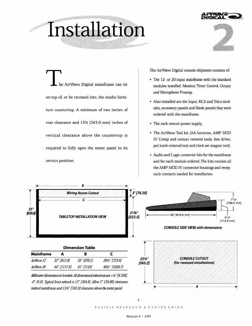
Te AirWave Digital mainframe can sit
on top of. or be recessed into. the studio furni-
ture countertop. A minimum of two inches of
rear clearance and 13~ (343.0 mm) inches of
vertical clearance above the countertop is
required to fully open the meter panel to its
service position.
1-4-] .. ------- 8 ----------t>~1
The AirWave Digital console shipment consists of:
• The 12- or 20-input mainframe with the standard
modules installed: Monitor, Tl.IIler Control, Output
and Microphone Preamp.
• Also installed are the Input. RLS and Telco mod
ules. accessory panels and blank panels that were
ordered with the mainframe.
• The rack-mount power supply.
• The AirWave Tool kit (AA batteries. AMP MOD
IV Crimp and contact removal tools. hex driver.
pot knob removal tool and clock set magnet tool) .
• Audio and Logic connector kits for the mainframe
and for each module ordered. The kits contain all
the AMP MOD IV connector housings and recep
tacle contacts needed for installation.
-1- ./ . .... . .... "Wiring ... .lIcce..... sScut.OUL·· :' 'IfH [76.20J ...... / ......... ...... .' ...... ....... .... ..... .., ..... /
__ 71/2" J+tmm1
Dimension Table
Mainframe A B C
AirWave-12 32" [812.8J 33" [838.2J 28].2" [723.9J
AirWave-20 44" [1117.6J 45" [1143J 40W' [1028.7J
Millimeterdimensiomin brackets.ADdimensionaJ toJerancesare +!4 "[6.350J,
-0" [0. 0]. ljpical front setback is 12" [304.8]. ADow 2" [50.80J dearance
behind mainframe and 13].2" [342.9J dearance above the meter panel
r 22W
[565.2J
------I~ 41/2'
[114.3mm]
CONSOLE SIDE VIEw, with dimensions
l~~ 14-1 .. ------- A ------~~I
PACIFIC RESEARC H & ENGINE ERING
Revision A • 3/99
To simplify console installation, logic cable wir
ing diagrams for specific peripheral equipment are
available from PR&E. Custom engraving for the
button caps and colored fader knobs are also avail
able. See Chapter 7, Accessories, for details.
INSTALLATION NOTE: Do not locate the con
sole near intense electromagnetic hum fields, such
as those produced by large power transformers
and by audio amplifiers which use inexpensive
power transformers operating in or near satura
tion. Strong electromagnetic fields may impair the
performance of AirWave Digital and neighboring
equipment. Audio cables must also be routed to
achieve maximum practical distance from all AC
power mains wiring.
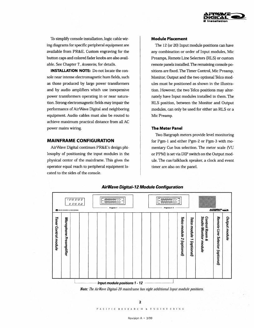
MAINFRAME CONFIGURATION AirWave Digital continues PR&E's design phi
losophy of positioning the input modules in the
physical center of the mainframe. This gives the
operator equal reach to peripheral equipment lo
cated to the sides of the console.
II Inahnetllan
Module Placement
The 12 (or 20) Input module positions can have
any combination or order of Input modules, Mic
Preamps, Remote Line Selectors (RLS) or custom
remote panels installed. The remaining console po
sitions are fixed. The Timer Control, Mic Preamp,
Monitor, Output and the two optional Telco mod
ules must be positioned as shown in the illustra
tion. However, the two Telco positions may alter
nately have Input modules installed in them. The
RLS position, between the Monitor and Output
modules, can only be used for either an RLS or a
MicPreamp.
The Meter Panel
Two Bargraph meters provide level monitoring
for Pgm-l and either Pgm-2 or Pgm-3 with mo
mentary Cue bus selection. The meter scale (VU
or PPM) is set via DIP switch on the Output mod
ule. The cue/talkback speaker, a clock and event
timer are also on the panel.
AirWave Oigital-12 Module Configuration
! II::-~-~~:'::::~:: -II I I
II:-~-~-~'::'::::~~: :11 I
1/2:00:00 I 00:00.0 _.f
~2/.!
eMCIFlC_.iNCIINIiDlNG I!l;f=:r~
§' ~ ;t ;t ~g ~ ~ S- S- 3 .g ~ .g ~:3 Q c:: ~ ~ 3 ~;;
iir -g § ,... 3 ::s ~ ::s Q i' I =: III iii iii -'~ a ~
8' ~ 3 N .... "'Qo
§ III Q' 0' ~ if .g "tI "tI -g. g. ~ ~ iii §i ~ ~ iii Q' ~ "tI .;::. .;::. g.
~ .;::.
L-----Input module positions 1-12 -------"
Note: The AirWave Digital-20 mainframe has eight additional Input module positions.
2
PACIFIC RESEARC H & ENGINE ERING
Revision A • 3/99
CONNECTOR ACCESS The meter panel is set into its service position
to access the module connectors. To move the meter
panel to its service position, Simultaneously press
on the latch buttons, located on the ends of the
meter panel, while lifting and rotating the panel
rearward.
Note: When opened to its service position, ex
ercise caution to ensure the panel does not acci
dentally fall closed.
To ease initial wiring, the meter panel can be
completely removed from the mainframe chassis.
Set the panel to its service position and unplug all
meter panel cabling to the speaker, meters and
clock/timer. With another person holding the meter
panel unlatch the two hinges, by moving the two
release pins into their detent positions, to free the
meter panel. To reinstall the meter panel, first align
the hinge parts together and then release the pins
out of their detents.
POWER SUPPLY The power supply is typically rack mounted in
the console cabinetry below and to the left or right
of the supporting countertop. The power supply
must be installed so that the ten-foot DC power
cable, that is fastened to the right end of the main
frame motherboard, is not under tension.
DC GROUNDING NOTE: The DC outputs of the
power supply are not referenced to the power sup
ply chassis and, therefore, are floating from the
AC safety ground. Do Not Connect audio or logic
supply ground wiring to the chassis of the power
supply.
AC GROUNDING NOTE: Do not defeat the
safety ground in any way. Doing so may proVide a
potentially dangerous condition to the operator.
3
~i=nY.&'DL::-:--
"iGiL~~ > 2 Ina1:alla1:lan
Refer to the AirWave Universal Power Supply Technical
Manual (PR&E # 75-41) for complete power sup
ply installation details.
GROUNDING & SHIELDING The broadcast facility's technical ground should
only connect to the mainframe chassis ground stud.
The stud is located next to the DC power supply
cable entry point into the chassis. Terminate the
facility's technical ground wire in a crimped lug.
Connect the audio shields at both the console
and the peripheral when all system components
share a common ground potential and are using
isolated ground AC outlets tied individually back
to the main technical ground.
If isolated ground AC outlets are not available,
connect the cable shields at the console end only.
The shields should be floated (left unconnected)
at the peripheral device. Ensure the peripheral
devices connect to a clean ground through their
power cords, or through separate ground wires to
the facility's technical ground.
POWER SUPPLY GROUNDING NOTE: The
power supply chassis is connected to the safety or
"U" ground wire in the AC mains supply cable.
Audio signals are not referenced to this ground in
any way by the console.
AUDIO GROUND NOISES: Buzz pickup is gen
erally electrostatic-such as capacitive coupling
between an audio line and a power line. Do not
route audio lines in the same wireway as an AC
power line.
PACIFIC RESEARCH & ENGINEERING
Revision A • 3/99
INSTALLING BACKUP BATTERIES Two AA batteries are supplied in the Installa
tion Tool Kit. They supply a "Keep Alive" voltage
that holds each module's logic state during mo
mentary power outages. They mount in battery
clips on the Timer Control module circuit board.
Observe the correct polarity (marked on the cir
cuit board) when installing the batteries.
Note: Replace batteries yearly to ensure con
tinuous backup protection. Remove one or both
batteries to prolong battery life when the console
will be unpowered for an extended period.
SETTING THE CLOCK The digital time-of-day clock can be a master
or a slave. In master mode, the factory preset, clock
timing is derived from a temperature
controlled quartz crystal oscillator. In slave mode,
clock timing is derived from a TC76/TC89-com
patible ESE master clock reference signal.
Master clocks are available from: ESE
142 Sierra St. EI Segundo, CA 90245.
Telephone: 310.322.2136 www.ese-web.com
The operating mode is set by switch S I, # 1 on
the clock/timer circuit board. To access the clock/
timer board, open the meter panel to its service
position. The clock/timer board is mounted be
hind the clock/timer display on the meter panel.
With the clock set to master mode, it's neces
sary to manually set the clock once power is ap-
ClocklTimer Option Switches
n ..... ' " , ."play On 1 N I -: I"' .'<pIay Off Clock: Master Mode ,......, I I Slave Mode
IS Switch 51, on the ClockiTimer printed circuit board, as viewed with the meter panel in its service position. Factory default settings shown.
4
2 Inatallation
plied to the console. Three magnetically-activated
Hall-effect sensors are used to adjust or hold the
time. They are positioned below and between each
pair of 7 -segment displays, just behind the dis
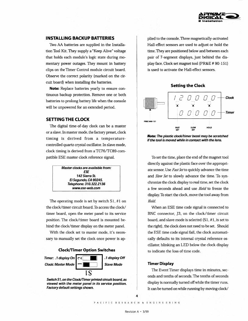
play face. Clock set magnet tool (PR&E # 90-151)
is used to activate the Hall-effect sensors.
PR&E#90-1S1
Setting the Clock
I Cl I
~
II '-I
FAST SET
II II '-I '-I
+" II II ,-I '-,
SLOW SET
II 11_ '-I '-'
I'
'-i
IIi 11-'-, '-'
HOLD
I-Clock
f--- Timer
Note: The plastic clock/timer bezel may be scratched if the tool is moved while in contact with the lens.
To set the time, place the end of the magnet tool
directly against the plastic face over the appropri
ate sensor. Use Fast Set to quickly advance the time
and Slow Set to slowly advance the time. To syn
chronize the clock display to real time, set the clock
a few seconds ahead and use Hold to freeze the
display. To start the clock, move the tool away from
Hold.
When an ESE time code signal is connected to
BNC connector, J3, on the clock/timer circuit
board, and slave mode is selected (S I, # I, is set to
the right), the clock does not need to be set. Should
the ESE time code signal fail, the clock automati
cally defaults to its internal crystal reference os
cillator, blinking an LED below the clock display
to indicate the loss of time code.
Timer Display
The Event Timer displays time in minutes, sec
onds and tenths of seconds. The tenths of seconds
display is normally turned off while the timer runs.
It can be turned on while running by moving clock/
PACIFIC RESEARCH & ENGINEERING
Revision A • 3/99
timer circuit board switch SI, #2, to the left. The
tenths of seconds are always displayed while the
timer is in the Stop or Hold modes, regardless of
the setting of switch S 1, #2.
Cabling & Wiring Before beginning the installation, draw a facil
ity wiring plan listing the console interconnections
with peripheral devices. Identify and create tags
for all audio and logic cabling. List each connec
tion in a master facility wiring logbook to facili
tate wiring installation, future system wiring
changes, equipment updates and system trouble
shooting. Refer to Module Connections, pages 17
through 23 later in this chapter, for the audio and
logic connector pin-out defmitions.
Analog audio connections require two-conduc
tor stranded, insulated, foil-shield cable contain
ing a separate shield drain wire (equivalent to
Belden 8451, 9451 or 8761).
AES/EBU connections require 110 ohm two
conductor stranded, insulated, foil-shield cable
containing a separate shield drain wire (equiva
lent to Belden 1800A).
Logic control cables require stranded, 22 AWe,
multiple conductor, non-shielded, jacketed cable
(equivalent to Belden 9423,8457 or 9421). The
number of conductors needed is determined by
the application. Typically five and eight wire cables
are most often used for constructing logic cables
(there are only 18 distinct signals on the LOgiC
Interface connector, of which only a handful may
actually be used for any given application).
WIRE PREPARATION All AirWave Digital audio and logic wiring ter
minates in AMP MOD IV receptacle contacts at
the console. Stranded wire of 22 to 26 AWe, with
insulation diameters of .040 to .060 inch, can be
used with the AMP MOD IV receptacle contacts.
5
Insulation Barrel
9/64"
~
~
AMP MOD IV Receptacle Contacts
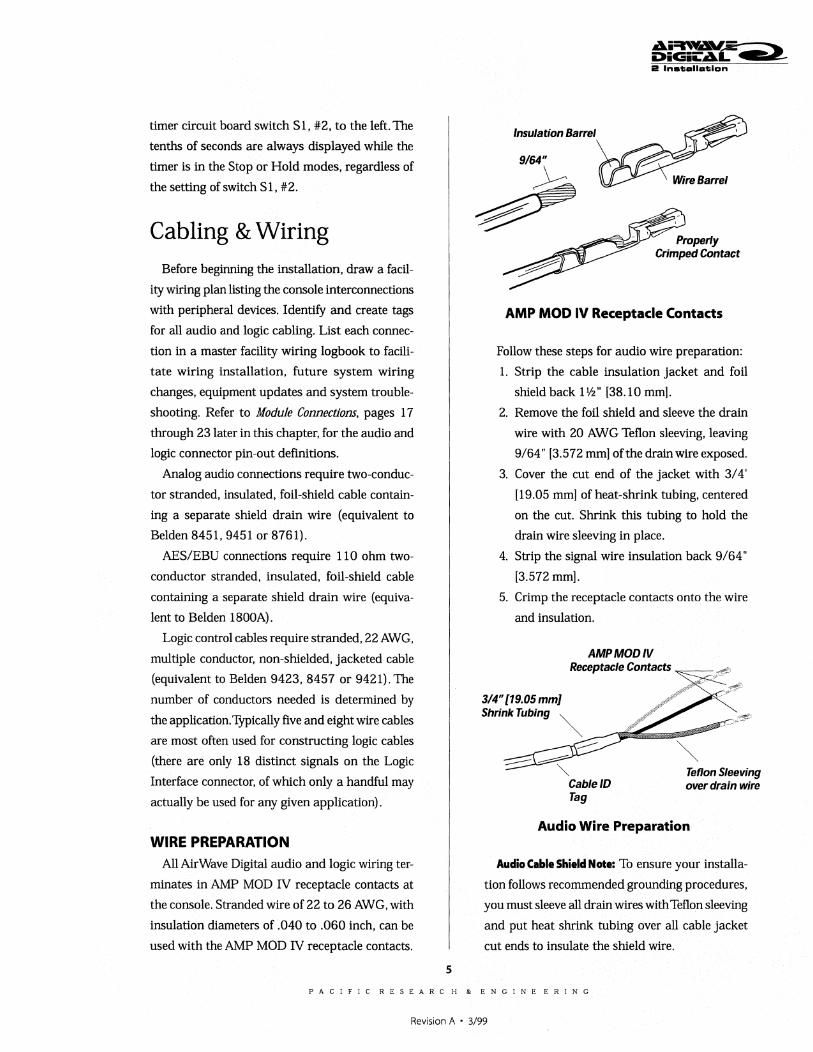
Follow these steps for audio wire preparation:
1. Strip the cable insulation jacket and foil
shield back IV2" [38.10 mmJ.
2. Remove the foil shield and sleeve the drain
wire with 20 AWe Teflon sleeving, leaVing
9/64" [3.572 mmJ of the drain wire exposed.
3. Cover the cut end of the jacket with 3/4'
[19.05 mmJ of heat-shrink tubing, centered
on the cut. Shrink this tubing to hold the
drain wire sleeving in place.
4. Strip the signal wire insulation back 9/64"
[3.572mmJ.
5. Crimp the receptacle contacts onto the wire
and insulation.
AMP MOD IV Receptacle Contacts
3/4" [19.05 mmJ Shrink Tubing ~
Teflon Sleeving over drain wire
Audio Wire Preparation
Audio Cable Shield Note: To ensure your installa
tion follows recommended grounding procedures,
you must sleeve all drain wires with Teflon sleeving
and put heat shrink tubing over all cable jacket
cut ends to insulate the shield wire.
PACIFIC RESEARC H 8< ENGINE ERING
Revision A • 3/99
Logic control cables are fabricated in a similar
manner to the audio wiring. Strip the jacket insu
lation back 1 W' [38.10 mm], sleeve the cut end
with 3/4" [19.05 mm] of shrink tubing and strip
the insulation from each wire 9/64" [3.572 mm].
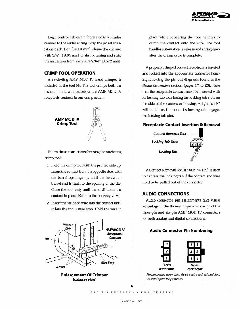
CRIMP TOOL OPERATION A ratcheting AMP MOD N hand crimper is
included in the tool kit. The tool crimps both the
insulation and wire barrels on the AMP MOD IV
receptacle contacts in one crimp action.
AMP MOD IV Crimp Tool
Follow these instructions for using the ratcheting
crimp tool:
1. Hold the crimp tool with the printed side up.
Insert the contact from the opposite side, with
the barrel openings up. until the insulation
barrel end is flush to the opening of the die.
Close the tool only until the anvil holds the
contact in place. Refer to the cutaway view.
2. Insert the stripped wire into the contact until
it hits the tool's wire stop. Hold the wire in
Die
AMP MOD IV Receptacle
Contact
.-~
Enlargement Of Crimper (cutaway view)
6
!Ii! Ina.ana.lan
place while squeezing the tool handles to
crimp the contact onto the wire. The tool
handles automatically release and spring open
after the crimp cycle is complete.
A properly crimped contact receptacle is inserted
and locked into the appropriate connector hous
ing following the pin-out diagrams found in the
Module Connections section (pages 17 to 23). Note
that the receptacle contact must be inserted with
its locking tab side facing the locking tab slots on
the side of the connector housing. A light" click"
will be felt as the contact's locking tab engages
the locking tab slot.
Receptacle Contact Insertion & Removal
Contact Removal TOOI--I '-::::--,
A Contact Removal Tool (PR&E 70-129) is used
to depress the locking tab if the contact and wire
need to be pulled out of the connector.
AUDIO CONNECTIONS Audio connector pin asSignments take visual
advantage of the three-pins-per-row design of the
three-pin and six-pin AMP MOD IV connectors
for both analog and digital connections.
Audio Connector Pin Numbering
~ .Ji6 2 2 5
1 14
3-pin connector
6-pin connector
Pin numbering shown from the wire entry end, oriented from the board operator s perspective.
PACIFIC RESEARC H & ENGINE ERING
Revision A • 3/99
When plugged into a module, the audio shields
are the pins closest to the console operator, the
audio low wires are the middle pins and the audio
high wires are the back pins. For stereo, the left
channel wires connect to the left column of pins
and the right channel wires to the right-hand col
umn of pins (all from the operator's perspective).
Microphone Inputs
Pin Signal Description 1 Shield (connects directly to the chassis) 2 Low (- input) 3 !Ugh (+ input)
Two-Channel Line Inputs and Outputs
Pin Signal Description 1 Shield for left channel or signal 1 2 Low (- input), left channel or signal 1 3 High (+ input), left channel or signal 1 4 Shield for right channel or signal 2 5 Low {- input}, right channel or signal 2 6 !Ugh (+ input), right channel or signal 2
Analog Connections
There are no analog interstage patch points
within the AirWave Digital input or output mod
ules. To use a patch bay, connect the line level out
puts from the peripheral devices directly to the
patch bay and then normal these to the appropri
ate analog Input modules. Likewise, AirWave
Digital's analog outputs may also be routed
through a patch bay normalled to standard pe
ripherals such as analog On-Air processing gear,
recorders, telephone hybrids, etc.
The Microphone Preamplifier module's line
level outputs (+4 dBu, nominal, balanced) can also
be routed through a patch bay normalled to an
Input module. If mic processing is reqUired, the
Preamplifier module's outputs may be routed
through line-level mic processing equipment and
then to an Input module. When mic-Ievel input
capable processors are used, the microphone
7
2 In.callaclan
should be connected to the mic processor with the
processor's line-level output directly connected to
an Input module.
Digital Connections
Digital outputs use three-pin connectors wired
like the Mic Inputs. These connections outputAES-
3 compatible signals (often referred to as AESI
EBU signals).
Note: The outputs cannot be directly connected
to a S/PDIF input. A Signal translation interface
must be used to do this.
AES/EBU Digital Outputs
Pin Signal Description 1 Shield (connects directly to the chassis) 2 Low {- input} 3 High (+input)
Because Input and RLS modules are available
with either an analog or a digital input, the con
nectors on these modules use six-pin AMP MOD
IV connectors even when the module is configured
for digital signals. Connect the AES/EBU signal
to pins 1, 2 and 3 only. There is no connection on
pins 4, 5 and 6.
AES/EBU Digital Inputs
Pin Signal Description 1 Shield for AESIEBU signal 2 Low (- input) 3 High (+input) 4 no connection 5 no connection 6 no connection
Routing digital audio signals through a patch
bay is not recommended.
PACIFIC RESEARC H & ENGINE ERING
Revision A • 3/99
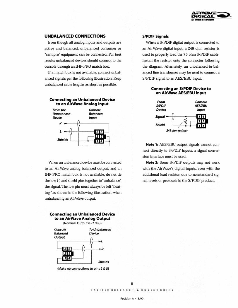
UNBALANCED CONNECTIONS
Even though all analog inputs and outputs are
active and balanced, unbalanced consumer or
"semipro" equipment can be connected. For best
results unbalanced devices should connect to the
console through an IHF -PRO match box.
If a match box is not available, connect unbal
anced signals per the following illustration. Keep
unbalanced cable lengths as short as possible.
Connecting an Unbalanced Device to an AirWave Analog Input
From the Unbalanced Device
: = ~ Shields
Console Balanced Input
When an unbalanced device must be connected
to an AirWave analog balanced output, and an
IHF-PRO match box is not available, do not tie
the low (-) and shield pins together to "unbalance"
the signal. The low pin must always be left "float
ing," as shown in the following illustration, when
unbalancing an AirWave output.
Connecting an Unbalanced Device to an AirWave Analog Output
(Nominal Output is -2 dBu)
Console To Unbalanced Balanced Device
OuC~ y :: ~mr I L . Shields
(Make no connections to pins 2 & 5)
8
e Inatallatlon
S/PDIF Signals
When a S/PDlF digital output is connected to
an AirWave digital input, a 249 ohm resistor is
used to properly load the 75 ohm S/PDlF cable.
Install the resistor onto the connector following
the diagram. Alternately, an unbalanced-to-bal
anced line transformer may be used to connect a
S/PDlF signal to an AES/EBU input.
Connecting an S/PDIF Device to an AirWave AES/EBU Input
From S/PDIF Device
Console AESIEBU
Input
::~. f ,A c;. 249 ohm resistor
Note 1: AES/EBU output Signals cannot con
nect directly to S/PDlF inputs, a Signal conver
sion interface must be used.
Note 2: Some S/PDlF outputs may not work
with the AirWave's digital inputs, even with the
additional load resistor, due to nonstandard sig
nallevels or protocols in the S/PDlF product.
PACIFIC RESEARC H & ENGINE ERING
Revision A • 3/99
LOGIC CONNECTIONS Each Input module comes standard with one
24-pin logic connector to control a device con
nected to either the A or B input. The optional 99-
1003 Dual Logic Interface plug-in can be added
to any Input module to provide a separate logic
connection for each input.
When a peripheral device is connected, one of
the main functions of the logic interface is to start
the peripheral at module on. The peripheral de
vice logic can, in turn, control the Input module;
turning the module audio off at the end of an event
and then controlling the Off lamp illumination to
indicate the peripheral device status.
When a Guest Panel is connected, its remote
On, Off, Cough and Talkback buttons control the
module while the logic control outputs from the
module control the button tallies in the Guest
Panel.
2 Inatallation
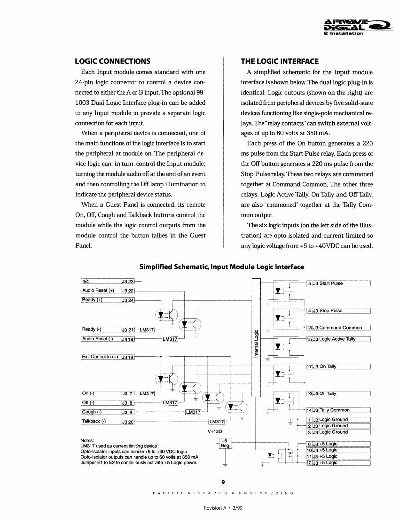
THE LOGIC INTERFACE A Simplified schematic for the Input module
interface is shown below. The dual logic plug-in is
identical. Logic outputs (shown on the right) are
isolated from peripheral devices by five solid-state
devices functioning like Single-pole mechanical re
lays. The "relay contacts" can switch external volt
ages of up to 60 volts at 350 rnA.
Each press of the On button generates a 220
ms pulse from the Start Pulse relay. Each press of
the Off button generates a 220 ms pulse from the
Stop Pulse relay. These two relays are commoned
together at Command Common. The other three
relays, Logic Active Tally, On Tally and Off Tally,
are also "commoned" together at the Tally Com
monoutput.
The six logic inputs (on the left side of the illus
tration) are opto-isolated and current limited so
any logic voltage from +5 to +40VDC can be used.
Simplified Schematic, Input Module Logic Interface
I nlc IJ3123~
I Audio Reset (+) IJ3122!
Ready (+) J324
IReady(-) IJ3121~
I Audio Reset (-) iJ31191-[LM\317
[!:I E~xtQ. C~o~n~tro~1 }!lni](+B)IJ4IJ3~11Uau-I---- 1-(~.: •.. ,-----t--------_'\ I -----t-------1
j. ) I'" O=n-'(---) ------.,IJ703TCI7"'~:--c~ (
I Off (-) IJ31a I
I Cough (-) iJ3[ 9 [
[Talkback (-) iJ3[20[
Notes: LM317 used as current limiting device Opto-Isolator inputs can handle +5 to +40 VDC logic Opto-Isolator outputs can handle up to 60 volts at 350 mA Jumper E1 to E2 to continuously activate +5 Logic power.
V+12D
T
9
!H 5 iJ31Start Pulse I I
L-h I I~~~~~------,
~ 1 !J3iL09iC Ground - , 2 IJ3 Logic Ground ~ 3 !J3[Logic Ground
] I [
PACIFIC RESEARCH & ENGINEERING
Revision A • 3/99
The On, Off, Cough and Talkback inputs allow
remote mic panel switches to control the Input
module through active low logic signals (pull to
ground). To enable these inputs jumper the Exter
nal Control In (+) connection to +5 Logic.
The Audio Reset and Ready inputs can use ei
ther active low logic (pull to ground) or active high
logic (pull to + VDC) from peripheral devices. With
active high logic, Ready (-) and Audio Reset (-)
are tied to logic ground on the peripheral device.
Ready (+) and Audio Reset (+) then connect to
the appropriate logic outputs on the peripheral
device.
When active low logic is used by the peripheral
device, Ready (+) and Audio Reset (+) connect to
the lOgiC supply voltage on the peripheral device,
and Ready (-) and Audio Reset (-) connect to the
appropriate logic outputs.
In normal operation the +5 Logic supply is
turned off when the interface is not enabled for
the input selected. Circuit board pads El and E2
can be jumpered to supply +5 Logic voltage at all
times for special applications.
AirWave Digital Quick Logic Guides
Pages 13 through 16 offer quick guides to con
figuring the console logic. Page 13 contains an Air
Wave Digital Logic Interface Glossary, Logic Set
tings switch definitions and a copy of the simpli
fied logic schematic from the previous page. Pages
14, 15 and 16 show connection diagrams for a
Guest Panel (remote mic panel), a CD player and
a digital delivery system, respectively.
Note: To completely isolate the console from a
peripheral device, use only the control input and
output connections. These are decoupled from the
console's ground and power supply through opto
isolator devices.
The Logic Ground and +5 Logic connections
are referenced to the console's logic power supply
and ground. Connect these only to a peripheral
10
Ai=n~- = ~iC;iiLA~ _ > 2 Inat;allat;ion
device with isolated logic connections or to a Guest
Panel. Connecting these to a non-isolated periph
eral device can result in a ground loop between
the console and the peripheral.
Input Module Logic and Microphones
The two main functions of microphone logic are
to automatically mute the monitor speakers in the
room with the "hot" mic and to command the ap
propriate hot mic warning light.
The warning commands come from the Moni
tor module, but it is the first four Logic Settings
switches on each Input module that tell the moni
tor module whether the A and/or B input is a con
trol room or a studio microphone.
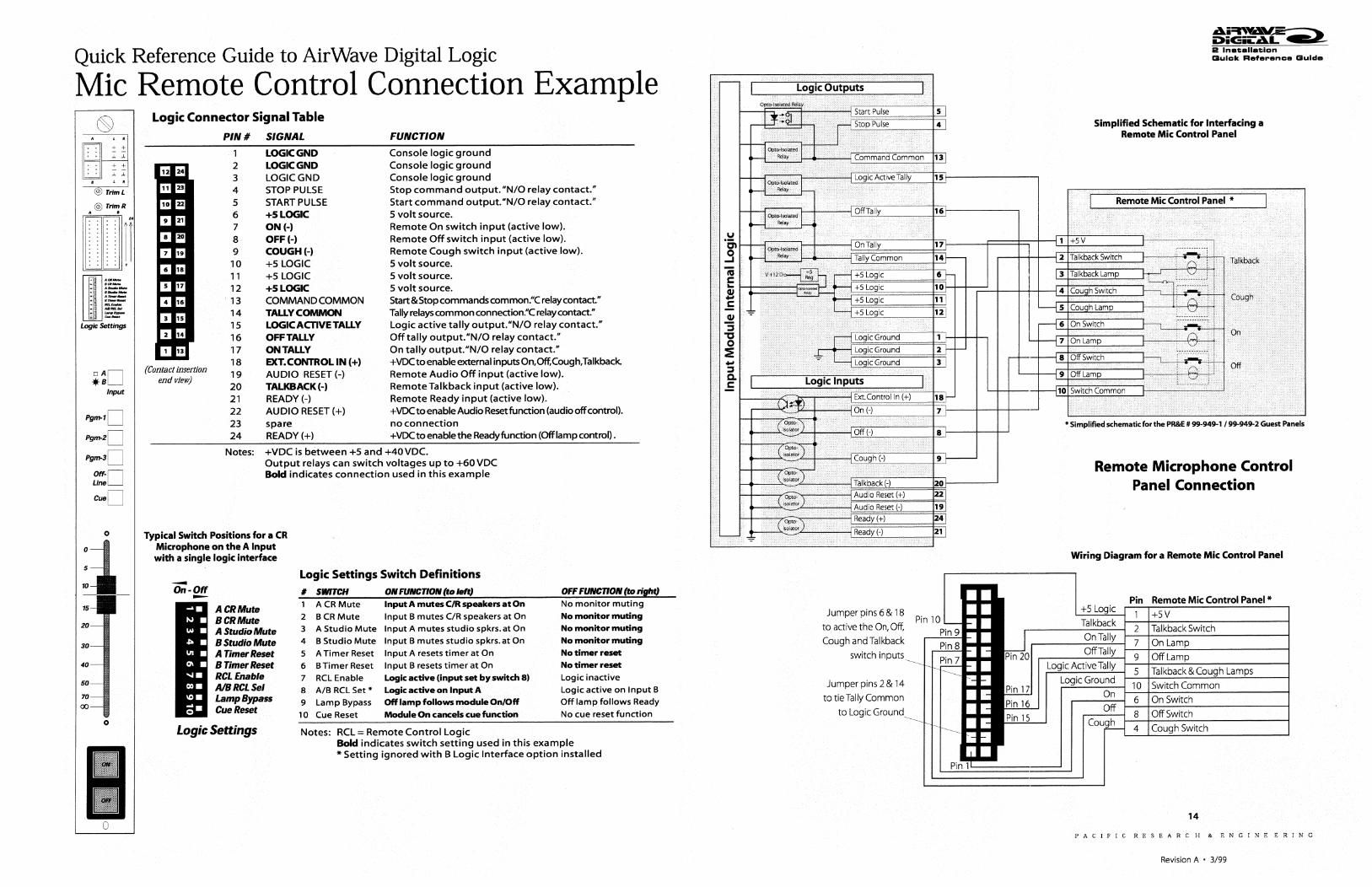
Page 14 summarizes setting up an Input mod
ule as a microphone input. To activate the Guest
Panel logic functions, turn on Logic Settings switch
7 and set switch 8 for the appropriate A or B in
put. To enable the remote control inputs (On, Off,
Cough,Talkback) ,jumper External Contro11n (+)
to +5 Logic on the logiC connector.
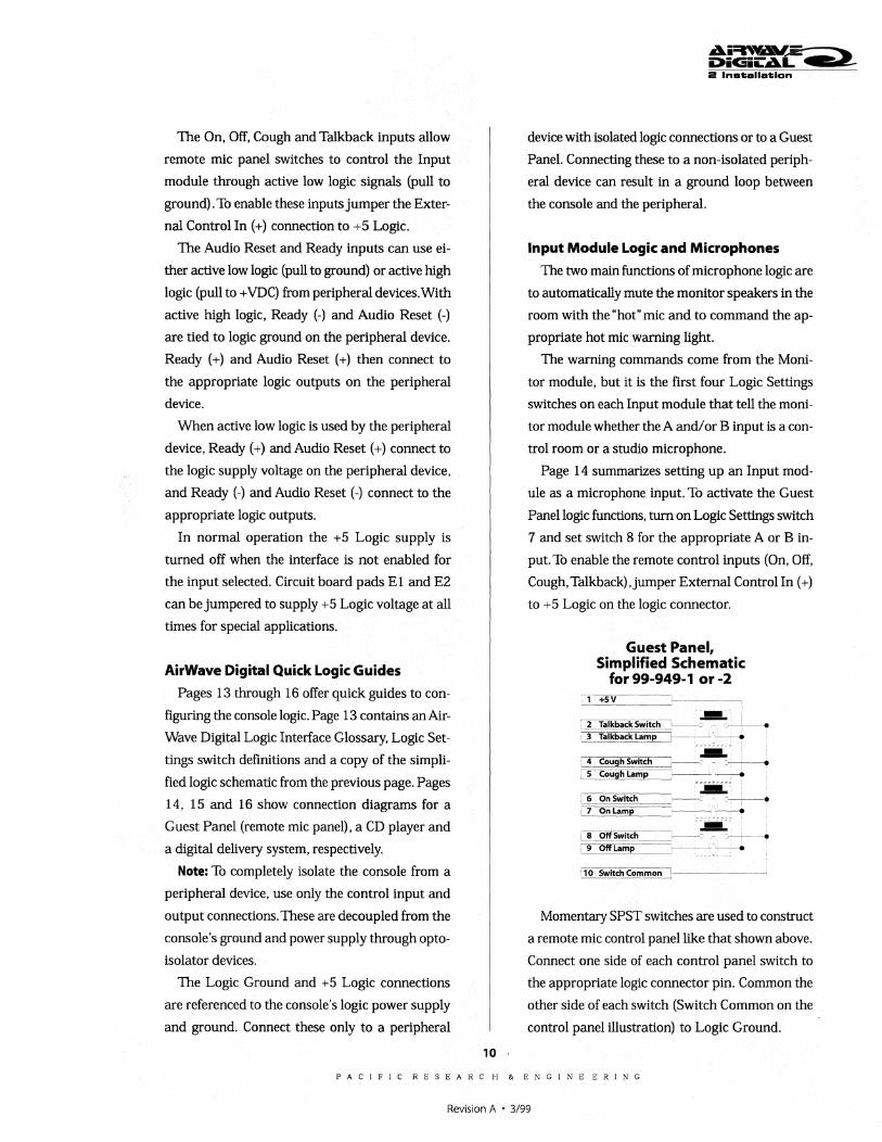
Guest Panel, Simplified Schematic
for 99-949-1 or-2 • 1 i+5V-------------
----------- -.... 2 Talk,,~w~ _1----'- c~ --.
2.!ali<tlacl<l:arn~. ---- c __ •
______________ -l!!!!IL-. _4~,,9I1.!i .. itch __ -~ --_ --. . 5 <:".iJ9J1.tamp .---- c.---e
Momentary SPST switches are used to construct
a remote mic control panel like that shown above.
Connect one side of each control panel switch to
the appropriate logic connector pin. Common the
other side of each switch (Switch Common on the
control panel illustration) to Logic Ground.
PACIFIC RESEARCH & ENGINEERING
Revision A • 3/99
The Logic Active Tally output controls the lamps
for the Cough andTalkback switches. The On Tally
and OfITally outputs control the On and Off switch
lamps. The other side of each lamp (+5 V) con
nects to +5 LogiC. Use 6.3 volt lamps, with less
than 50 rnA current draw, for all remote panels
supplied by the console.
Input Module Logic and Peripheral
Devices
Peripheral devices are controlled through the
Start, Stop and Command Common logic outputs.
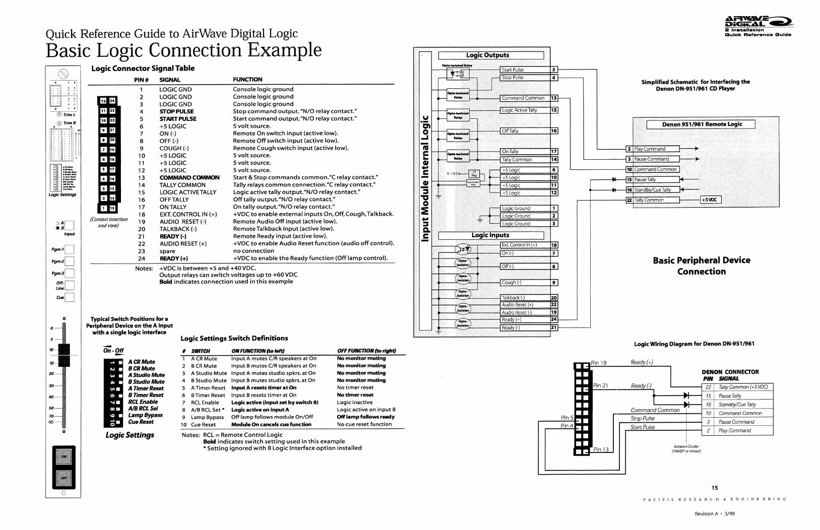
In the connection example on page 15, active
low logic is used, thus Command Common is con
nected to the logic ground on the peripheral de
vice (labeled command common by Denon).
In the example on page 16, active high logic is
required, thus Command Common is connected
to +5 Logic. Note that this voltage is more typi
cally supplied directly by the peripheral device to
prevent ground loops.
Peripheral devices control the module through
the Audio Reset and Ready logic inputs. On page
15, only the Ready function is shown being used.
Ready performs an Audio Reset, to turn off the
module without generating a Stop Pulse. in addi
tion to then controlling the Off lamp illumination.
On page 16,Audio Reset (+) and Ready (+) con
nect to +5 Logic on the module. The Ready (-)
command and the Audio Reset (-) command are
pulled low by the active low logic relay outputs on
the peripheral device, which all tie to the module's
Logic Ground (pin 1).
For peripheral devices that require a steady On
or Off signal, the On and Off tallies can be used.
When the Off Tally is used in this manner, Logic
Settings switch #9 (Lamp Bypass) must be set to
the left (On) so that the Off lamp is not controlled
by the Ready logic.
11
~i~a'e => Ii! Ina.alla,don
ADDITIONAL LOGIC CONNECTIONS There are three additional AirWave Digital logic
connections on the Monitor module, Telco mod
ule and the Timer Control module.
An 8-pin connector on the Monitor module car
ries the logic control outputs for the Control Room
and Studio warning light interfaces. The Monitor
module logic connection and block diagram are
on the next page.
The Telco module includes a 3-pin connector
for a Start and a Stop Pulse output for triggering
a hybrid or other remote device at module on and
off.
A 3-pin connector on the Timer Control mod
ule carries the remote timer reset logic. The Timer
Control module logic connection and description
are in the Timer Module Remote Connection section
on page 23.
Monitor Module Logic
There is one 8-pin logic connector for the "hot
mic" logic command outputs for the Control Room
and Studio on-air warning lamp systems.
Each lOgiC command output is isolated using a
solid-state relay with a pair of normally open" dry
contacts." These reJay contacts can switch external
voltages of up to 60 volts at 350 mA for direct
interface to most lamp control devices.
If an external five volt lamp relay is used, one
side of the interface relay can be jumpered to +5
Volts (pins 2 and 6) or to Logic Ground (pins 1
and 5) to create an active high or active low out
put, respectively.
The simplified schematic on the next page shows
the logic outputs for the Control Room and Stu
dio warning lamp interface externally jumpered
to yield an active high output from the relay.
When an active low logic output is needed on
the Control Room, jumper pins 1 and 3 together
and use pin 4 as the Control Room warning out
put. Jumper pins 5 and 7 together and use pin 8
PACIFIC RESEARC H & ENGINE ERING
Revision A • 3/99
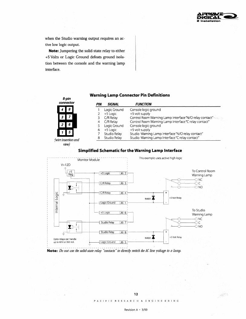
when the Studio warning output requires an ac
tive low logic output.
Note: Jumpering the solid-state relay to either
+5 Volts or Logic Ground defeats ground isola
tion between the console and the warning lamp
interface.
2 In."allatlon
B-pin connector
Warning Lamp Connector Pin Definitions
(wire insertion end \dew)
PIN SIGNAL
1 Logic Ground 2 +5 Logic 3 C/R Relay 4 C/R Relay 5 Logic Ground 6 +5 Logic 7 Studio Relay 8 Studio Relay
FUNCTION
Console logic ground +5 volt supply Control Room Warning Lamp Interface "N/O relay contact" Control Room Warning Lamp Interface "C relay contact" Console logic ground +5 volt supply Studio Warning Lamp I nterface "N/O relay contact" Studio Warning Lamp Interface"C relay contact"
Simplified Schematic for the Warning Lamp Interface
---------------------------------------I Monitor Module
V+12D
1--------..- (--,-+~5 =Lo2g",ic __ -=~
This example uses active high logic
To Control Room Warning Lamp
~,--(}-----() NC ~C
,--(}-----() NO
C--=::::J--II--I~CJI'fjR:J1R~el~aY~=TIJ6[114r-----I-__i + u "51 .s co E
"I Logic Ground J6 ~ I
r +5 Logic
IN4001 +5 Volt Relay
To Studio Warning Lamp ~I
H~+I-"I[}St§Ud§:"iO~Re§lla =:Jmj----T--1 ~~~ Opto·relays can handle up to 60V at 350 mA
I _
IN4001 +5 Volt Relay
1 _________ ~ _____________________________ I
Note: Do not use the solid-state relay "contacts" to directly switch the AC line yoltage to a lamp.
12
PACIFIC RESEARCH &E N GIN E E R I N G
Revision A • 3/99
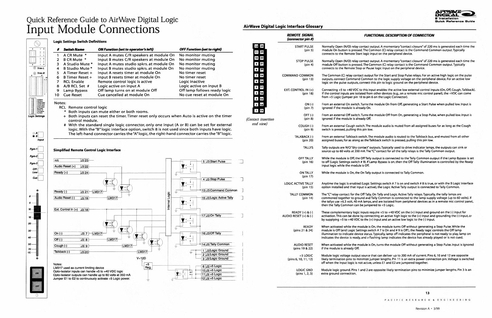
Quick Reference Guide to AirWave Digital Logic
Input Module Connections
+ +
" " + +
" " , R
OOil ill, ~
' .~-.. .ar ..... : === .. A_ .... .. Bn....., . "'-.. AlllIIICtSllf
. ---= --Logic Settings
DAO *B Input
Pgm-10 Pgm-20 Pgm-30 °"-0 Line
Cue 0
o
o
5
o
Logic Settings Switch Definitions
# SMtitchName ON Function (set to operaror~ left} OFF Function (set to right}
1 A CR Mute * Input A mutes C/R speakers at module On No monitor muting 2 8 CR Mute * Input 8 mutes C/R speakers at module On No monitor muting 3 A Studio Mute * Input A mutes studio spkrs. at module On No monitor muting 4 8 Studio Mute * Input 8 mutes studio spkrs. at module On No monitor muting 5 A Timer Reset + Input A resets timer at module On No timer reset 6 8 Timer Reset + Input 8 resets timer at module On No timer reset 7 RCL Enable Remote control logic is active Logic inactive 8 Al8 RCL Set # Logic active on input A Logic active on input B 9 Lamp Bypass Off lamp turns on at module Off Off lamp follows ready logic
10 Cue Reset Cue cancelled at module On No cue reset at module On
Notes; RCL Remote control logic
. * Both inputs can mute either or both rooms . + Both inputs can reset the timer. Timer reset only dccurs when Auto is active on the timer
control module. # With the standard single logic connector, only one input (A or B) can be set for external
logic. With the "B" logic interface option, switch 8 is not used since both inputs have logic. The left-hand connector carries the "A" logic, the right-hand connector carries the "8" logic.
Simplified Remote Control Logic Interface
1 nlc IJ3123i--
Audio Reset (+)
Ready (+)
1 Ext. Control In (+) u3118 r--------,~--~--~-----,
Notes: LM317 used as current limiting device Opto-Isolator inputs can handle +5 to +40 VDC logic Opto-Isolator outputs can handle up to 60 volts at 350 mA Jumper E1 to E2 to continuously activate +5 Logic power.
V+12D
J
]
"]
]
J
.a.i=nYaL;;;;-;;..---... i:»iGiL'.a.L'"" > II Inel:ellel:lan Buick Reference mulde
AirWave Digital Logic Interface Glossary
(Contact insertion end view)
REMOTE SIGNAL (connector pin #)
START PULSE (pin 5)
STOP PULSE (pin 4)
COMMAND COMMON (pin 13)
EXT. CONTROL IN (+) (pin 18)
ON (-) (pin 7)
OFF (-) (pin 8)
COUGH (-) (pin 9)
TALKBACK (-) (pin 20)
TALLYS
OFF TALLY (pin 16)
ON TALLY (pin 17)
LOGIC ACTIVE TALLY (pin 15)
TALLY COMMON (pin 14)
READY (+) & (-) AUDIO RESET (+) & (-)
READY (pins 21 & 24)
AUDIO RESET (pins 19 & 22)
+5 LOGIC (pins 6, 10, 11, 12)
LOGICGND (pins 1,2,3)
FUNCTIONAL DESCRIPTION OF CONNECTION
Normally Open (N/O) relay contact output. A momentary·contact closure" of 220 ms is generated each time the module On button is pressed. The Common (e) relay contact is the Command Common output. Typically connects to the Remote Start logic input'on the peripheral device.
Normally Open (N/O) relay contact output. A momentary "contact closure· of 220 ms is generated each time the module Off button is pressed. The Common (C) relay contact is the Command Common output. Typically connects to the Remote Stop or Pause logic input on the peripheral device.
The Common (C) relay contact output for the Start and Stop Pulse relays. For an active high logic on the pulse outputs, connect Command Common to the logic supply voltage on the peripheral device. For an active low logic on the pulse outputs,connect this pin to logic ground on the peripheral device.
Connecting +5 to +40 VDC to this input enables the active low external control inputs (On, Off, Cough, Talkback). If the control inputs are isolated from other devices (e.g., on a remote mic control panel), the +VDC can come from +5 Logic Oumper pin 18 to pin 6 on the Logic Connector).
From an external On switch. Turns the module On from Off, generating a Start Pulse when pulled low. Input is ignored if the module is already On.
From an external Off switch. Turns the module Off from On, generating a Stop Pulse, when pulled low. Input is ignored if the module is already Off.
From an external Cough switch. The module audio is muted from all assigned buses for as long as the Cough switch is pressed, pulling this pin low.
From an external Talkback switch. The module audio is routed to the Talkback bus, and muted from all other assigned buses, for as along as the Talkback switch is pressed, pulling this pin low.
Tally outputs are N/O "dry contact" outputs. Typically used to drive indicator lamps, the outputs can sink or source up to 60 volts at 350 mAo The"e" contact for all the tally relays is the Tally Common output.
While the module is Off. the Off Tally output is connected to the Tally Common output if the Lamp Bypass is set to off (Logic Settings switch It 9). If Lamp Bypass is on, then the Off Tally illumination is controlled by the Ready input logic while the module is Off.
While the module is On, the On Tally output is connected to Tally Common.
Anytime the logic is enabled (Logic Settings switch # 7 is on and switch # 8 is true, or with the B Logic Interface option installed and that input is active), the Logic Active Tally output is connected to Tally Common.
The Me" relay contact for the Off Tally, On Tally and Logic Active Tally relays. Typically, the tally lamps are commoned together to ground and Tally Common is connected to the lamp supply voltage (up to 60 volts). If the tallys use +6.3 volt, 40 mA lamps, and are isolated from peripheral devices as in a remote mic control panel, then the Tally Common can be jumpered to +5 Logic.
These complementary logic inputs require +5 to +40 VDC on the (+) input and ground on the (-) input for activation. This can be done by cO'lnecting an active high logic to the (+) input and grounding the (-) input, or by supplying +5 to +40 VDC to the, (+) input and an active low logic to the (-) input.
When activated while the module is On, the module turns Off without generating a Stop Pulse. While the module is Off (and Logic Settings switch # 7 is On and It 9 is Off), the Ready logic controls the Off lamp illumination to indicate device status. Typically, lamp off indicates the peripheral is not ready to play, lamp on indicates the device is ready, and a flashing lamp indicates the device has already played or is not cued.
When activated while the module is On, turns the module Off without generating a Stop Pulse. Input is ignored if the module is already Off.
Module logic voltage output source that can deliver up to 200 mA of current. Pins 6, 10 and 12 are opposite likely termination pins to minimize jumper lengths. Pin 11 is an extra power connection pin. Voltage is switched off when the Input logic is not active, unless El and E2 are jumpered together.
Module logic ground. Pins 1 and 2 are opposite likely termination pins to minimize jumper lengths. Pin 3 is an extra ground connection.
13
PACIFIC RESEARC H & ENGINE ERING
Revision A • 3/99
Quick Reference Guide to AirWave Digital Logic
Mic Remote Control Connection Example
tlrlil [jJ. ~
" .~-... ar .... ............. .. . ........... .. A~_ - ._-. --• MIICt..,
- -ci a. ...
LogiC Sertlngs
DAO *B Input
Pgm-10
Pgm-20 Pgm-30
°"-0 LIne
Cue 0
o
o
5
o
Logic Connector Signal Table PIN# SIGNAL FUNCTION
(Contact insertion end view)
2 3 4 5 6 7 8 9 10 11 12
, 13
14 15 16 17 18 19 20 21 22 23 24
LOGICGND LOGICGND LOGICGND STOP PULSE START PULSE +SLOGIC ON(-) OFF(-) COUGH(-) +5 LOGIC +5 LOGIC +SLOGIC COMMAND COMMON TALLY COMMON LOGIC ACTIVE TALLY OFF TALLY ON TALLY EXT. CONTROL IN (+) AUDIO RESET (-) TALKBACK(-) READY (-) AUDIO RESET (+) spare READY(+)
Console logic ground Console logic ground Console logic ground Stop command output. "N/O relay contact." Start command output."N/O relay contact." 5 volt source. Remote On switch input (active low). Remote Off switch input (active low). Remote Cough switch input (active low). 5 volt source. 5 volt source. 5 volt source. Start & Stop commands common."C relay contact" Tally relays common connection."C relay contact" Logic active tally output. "N/O relay contact." Off tally output."N/O relay contact." On tally output."N/O relay contact." +VDCto enable extemal inputs On, Off,Cough,Talkback. Remote Audio Off input (active low). Remote Talkback input (active low). Remote Ready input (active low). +VOCto enable Audio Reset function (audio offcontrol). no connection +VDC to enable the Readyfunction (Off lamp control) .
Notes: +VDC is between +5 and +40VDC. Output relays can switch voltages up to +60VDC Bold indicates connection used in this example
Typical Switch Positions for a CR Microphone on the A Input with a single logic interface
-On-Off -ACRMute BCRMute A Studio Mute B Studio Mute A Timer Reset B Timer Reset RCLEnabie AlBRCLSel Lamp Bypass Cue Reset
Logic Settings
Logic Settings Switch Definitions # SMTCH ON FUNCTION (to .. ttl OFF FUNCnON (to right}
1 ACR Mute Input A mutes e/R speakers at On No monitor muting
2 BCR Mute Input B mutes C/R speakers at On No monitor muting 3 A Studio Mute Input A mutes studio spkrs. at On No monitor muting 4 B Studio Mute Input B mutes studio spkrs. at On No monitor muting 5 ATimer Reset Input A resets timer at On No timer reset 6 B Timer Reset Input B resets timer at On No timer reset 7 RCL Enable Logic active (input set by switch 8) Logic inactive
8 AlB RCLSet * Logic active on Input A Logic active on Input B
9 Lamp Bypass Off lamp follows module On/Off Off lamp follows Ready
10 Cue Reset Module On cancels cue function No cue reset function
Notes: RCL:::: Remote Control Logic Bold indicates switch setting used in this example * Setting ignored with B Logic Interface option installed
Jumper pins 6 & 18
to active the On, Off. Cough and Talkback
switch
to Logic
.4i=l MlIW!'=-:--.... ~iGiL.4~ > Ii! Inatssllstslan Glulck Rafaranca Guida
Simplified Schematic for Interfacing a Remote Mic Control Panel
* Simplified schematic for the PR&E # 99-949-1/99-949-2 Guest Panels
Remote Microphone Control Panel Connection
Wiring Diagram for a Remote Mic Control Panel
14
PACIFIC RESEARC H & ENCINE ERINC
Revision A • 3/99
Quick Reference Guide to AirWave Digital Logic
Basic Logic Connection Example
D·: + + .J. .J.
D·: + + .J. .J. 1 •
@ TrimL
~l ill, ~
" ... -.. ear_ .. Aa.-_ ......... -.. An..w-...a · .~ ... · --• 1IM1ICl.,
· --;;: cu. ....
Logic Settings
Input
pgm-1D
Pgm-zD Pgm-3D
O"-D Line
CueD
o
o
5
o
Logic Connector Signal Table
12 24
11 23
10 22
• 21
8 20
7 1.
6 18
5 17
4 16
3 15
2 14
1 13
(Contact insertion end view)
PIN# SIGNAL FUNCTION
1 2 3 4 5 6 7 8 9 10 11 12 13 14 15 16 17 18 19 20 21 22 23 24
LOGICGND LOGICGND LOGICGND STOP PULSE START PULSE +5 LOGIC ON (-) OFF (-) COUGH (-) +5 LOGIC +5 LOGIC +5 LOGIC COMMAND COMMON TALLY COMMON LOGIC ACTIVE TALLY OFF TALLY ON TALLY EXT. CONTROL IN (+) AUDIO RESET (-) TALKBACK (-) READY(-) AUDIO RESET (+) spare READY(+)
Console logic ground Console logic ground Console logic ground Stop command output_ "NtO relay contact." Start command output. "NtO relay contaCt." 5 volt source. Remote On switch input (active low). Remote Off switch input (active low). Remote Cough switch input (active low). 5 volt source. 5 volt source. 5 volt source. Start & Stop commands common."C relay contact." Tally relays common connection."C relay contact." Logic active tally output."NtO relay contact." Off tally output.uNtO relay contact." On tally output. UNtO relay contact." +VDC to enable external inputs On, Off, Cough, Talkback. Remote Audio Off input (active low). Remote Talkback input (active low). Remote Ready input (active low). +VDC to enable Audio Reset function (audio off control). no connection +VDC to enable the Ready function (Off lamp control).
Notes: +VDC is between +5 and +40VDC. Output relays can switch voltages up to +60 VDC Bold indicates connection used in this example
Typical Switch Positions for a Peripheral Device on the A Input
with a single logic interface Logic Settings Switch Definitions -On-Off -
ACRMute BCRMute A Studio Mute B Studio Mute A Timer Reset B Tuner Reset RCLEnable AlBRCLSel Lamp Bypass Cue Reset
Logic Settings
# SWITCH ON FUNCnON (to left) OFF FUNCnON (to rigid} ACRMute Input A mutes C/R speakers at On No monitor muting
2 BCRMute Input B mutes C/R speakers at On No monitor muting
3 A Studio Mute Input A mutes studio spkrs.at On No monitor muting 4 B Studio Mute Input B mutes studio spkrs. at On No monitor muting 5 A Timer Reset Input A resets timer at On No timer reset
6 B Timer Reset Input B resets timer at On No timer reset 7 RCLEnabie Logic active (input set by switch 8) Logic inactive
8 AlBRCL Set * Logic active on input A Logic active on input B
9 Lamp Bypass Off lamp follows module On/Off Off lamp follows ready 10 Cue Reset Module On cancels cue function No cue reset function
Notes: RCL = Remote Control Logic Bold indicates switch setting used in this example * Setting ignored with B Logic Interface option installed
Logic Outputs
5
4
P""P"" Pin 19 .. .. l- I-l- I- Pin 21
I- ~ l- I-l- I-
PinS .. .. Pin 4 l- I-
l- I-l- • .. .. Pin 13 --
Simplified Schematic for Interfacing the Denon DN-951/961 CD Player
Basic Peripheral Device Connection
Logic Wiring Diagram for Denon DN-951 1961
) Ready(+
DENON CONNECTOR PI. SlGIVAL
Ready(-) 22 Tally Common (+5 VDC) 1 ...
15 Pause Tally I ~~ 16 Standby/Cue Tally
Command Common 10 Command Common
Stop Pulse 3 Pause Command
Start Pulse 2 Play Command
lsalation Diodes (lN4001 Drsimilar)
15
PACIFIC RESEARC H & ENGINE ERING
Revision A • 3/99
Quick Reference Guide to AirWave Digital Logic
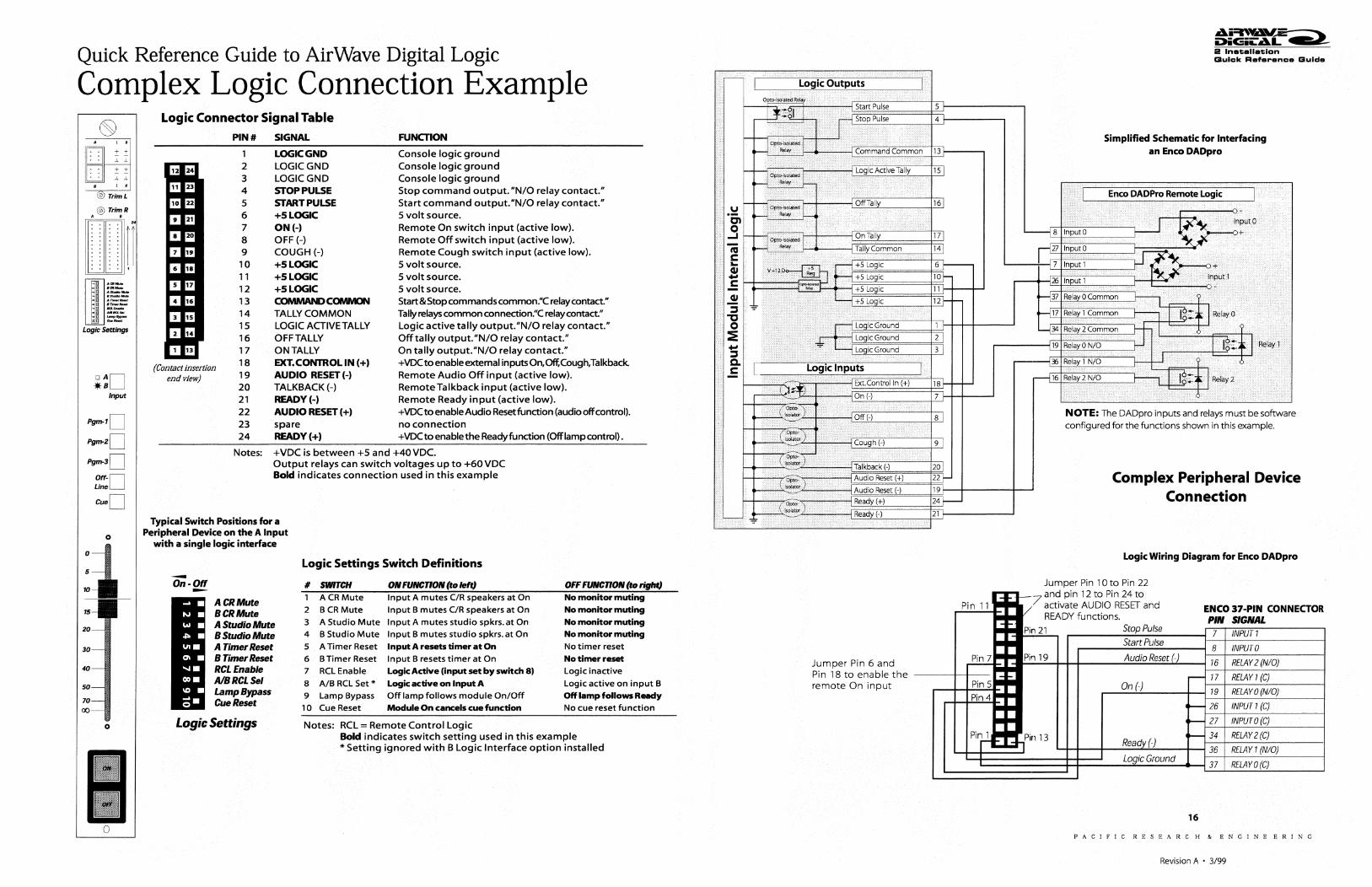
Complex Logic Connection Example
[J.: + + ,j, ,j,
+ + ,j, ,j,
Logic Settings
Input
o
o
5
20
o
Logic Connector Signal Table
(Contact insertion end view)
PIN#
1 2 3 4 5 6 7 8 9 10 11 12 13 14 15 16 17 18 19 20 21 22 23 24
SIGNAL
LOGICGND LOGICGND LOGICGND STOP PULSE START PULSE +5 LOGIC ON(-) OFF (-) COUGH (-) +5 LOGIC +5 LOGIC +5 LOGIC COMMANDCCIIIIMON TALLY COMMON LOGIC ACTIVE TALLY OFFTALLY ON TALLY EXT. CONTROL IN (+) AUDIO RESET (-) TALKBACK (-) READY(-) AUDIO RESET (+) spare READY(+)
FUNCTION
Console logic ground Console logic ground Console logic ground Stop command output. "NtO relay contact." Start command output. UNtO relay contact." 5 volt source. Remote On switch input (active low). Remote Off switch input (active low). Remote Cough switch input (active low). 5 volt source. 5 volt source. 5 volt source. Start & Stop commands common."C relay contact" Tally relays common connection.UC relay contact." Logic active tally output."NtO relay contact." Off tally output. UNtO relay contact." On tally output. UNtO relay contact." +VDCtoenableextemalinputsOn,Off,Cough,Talkback. Remote Audio Off input (active low). Remote Talkback input (active low). Remote Ready input (active low). +VDCto enable Audio Reset function (audio off control). no connection +VDCtoenablethe Readyfunction (Off lamp control) .
Notes: +VDC is between +5 and +40 VDC. Output relays can switch voltages up to +60 VDC Bold indicates connection used in this example
Typical Switch Positions for a Peripheral Device on the A Input
with a single logic interface
-On-Off -ACRMute BCRMute A Studio Mute B Studio Mute A Timer Reset B Timer Reset RCLEnable AlBRCLSeI Lamp Bypass Cue Reset
Logic Settings
Logic Settings Switch Definitions
# SINITCH ON FUNCnON (to IeftJ OFF FUNCDON (to rightJ 1 A CRMute Input A mutes C/R speakers at On No monitor muting 2 BCR Mute Input B mutes c/R speakers at On No monitor muting 3 A Studio Mute Input A mutes studio spkrs. at On No monitor muting 4 B Studio Mute Input B mutes studio spkrs.at On No monitor muting 5 ATimer Reset Input A resets timer at On No timer reset 6 B Timer Reset Input B resets timer at On No timer reset 7 RCLEnabie Logic Active (input set by switch 8) Logic inactive 8 AlBRCL Set * Logic active on Input A Logic active on input B 9 Lamp Bypass Off lamp follows module On/Off Off lamp follows Ready 10 Cue Reset Module On.cancels cue function No cue reset function
Notes: RCL = Remote Control Logic Bold indicates switch setting used in this example * Setting ignored with B Logic Interface option installed
.!::! c:n
..9
.. ::::s ~ c -
Jumper Pin 6 and Pin 18 to enable the remote On input
Pin 11
Pin 7
Pin 5
Pin 4
At.i=l\vat;;;;-....... --~iC;iLAt.~ > Iii! InataU.tlDn Buick Referance Guide
Simplified Schematic for Interfacing an Enco DADpro
NOTE: The DADpro inputs and relays must be software configured for the functions shown in this example.
Complex Peripheral Device Connection
Logic Wiring Diagram for Enco DADpro
Jumper Pin 10 to Pin 22 d -; - _. an pin 12 to Pin 24 to
•• /7 activate AUDIO RESET and ENCO 37-PIN CONNECTOR • • READY functions. PIN SIGNAL
• • Pin 21 Stop Pulse 7 INPUT1
• • Start Pulse 8 INPUT 0
• • Pin 19 Audio Reset (-) 16 RELAY 2 (NIO)
~ ~ :- 17 RELAY 1 (C) • • On (-) ~ ~
79 RELA Y 0 (NIO)
~ ~ - 26 INPUT 1 (C)
~ ~ I-- 27 INPUTO(C)
Pinr4 ~ .. Pin 13 Ready(-)
I-- 34 RELAY2(C)
- ~"'l 36 RELAY 1 (NIO) Logic Ground
37 RELAYO(C)
16
PACIFIC RESEARC H & ENGINE ERING
Revision A • 3/99
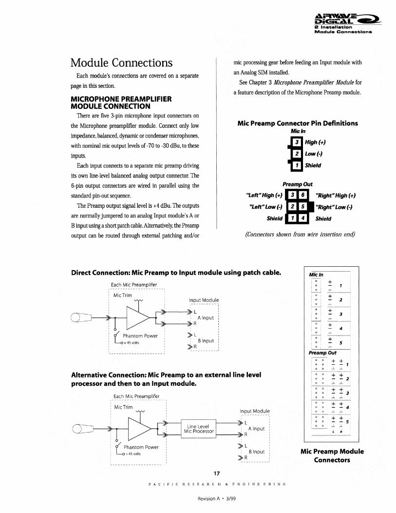
Module Connections Each module's connections are covered on a separate
page in this section.
MICROPHONE PREAMPLIFIER MODULE CONNECTION
There are five 3-pin microphone input connectors on
the Microphone preamplifier module. Connect only low
impedance, balanced, dynamiC or condenser microphones,
with nominal mic output levels of -70 to -30 dBu, to these
inputs.
Each input connects to a separate mic preamp driving
its own line-level balanced analog output connector. The
6-pin output connectors are wired in parallel using the
standard pin-out sequence.
The Preamp output signal level is +4 dBu. The outputs
are normally jumpered to an analog Input module's A or
B input using a short patch cable. Alternatively, the Preamp
output can be routed through external patching and/or
Ai=t\VAv.:':-::----i>iGiL'AL'" > 2 Inatoallatolon Module Conn.ctolona
mic processing gear before feeding an Input module with
an Analog SIM installed.
See Chapter 3 Microphone Preamplifier Module for
a feature description of the Microphone Preamp module.
Mic Preamp Connector Pin Definitions Micln
~Hi9h(+)
2 Low(-)
1 Shield
Preamp Out
"Left" High (+) 1i6 "Right" High (+)
"Left" Low (-) 2 5 "Right" Low (-)
Shield 1 4 Shield
(Connectors shown from wire insertion end)
Direct Connection: Mic Preamp to Input module using patch cable. Micln
Each Mic Preamplifer
: MicTrim
i ~ r' I,nput Module
CJJ~=~:~=====::AIOP",U : t:/ Phantom Power : : L-o + 45 volts :
>L : B Input
:>R , ~~------------
Alternative Connection: Mic Preamp to an external line level processor and then to an Input module.
Each Mic Preamplifer ,-- --- ---------------
MicTrim Input Module
~--~----~--~~L : A Input
~--~~~~--~R
t:/ Phantom Power L-o + 45 volts
17
>L : B Input
j,R
PACIFIC RESEARCH & ENGINEERING
Revision A • 3/99
+ -0
0 , + - 2
+ - 3
+ - 4 0 ~
0 + - 5
Preamp Out --
0 0 + + - - 1 )., ).,
+ + - - 2 0 0 )., ).,
0 0
).,
+ -+ -L R
Mic Preamp Module Connectors
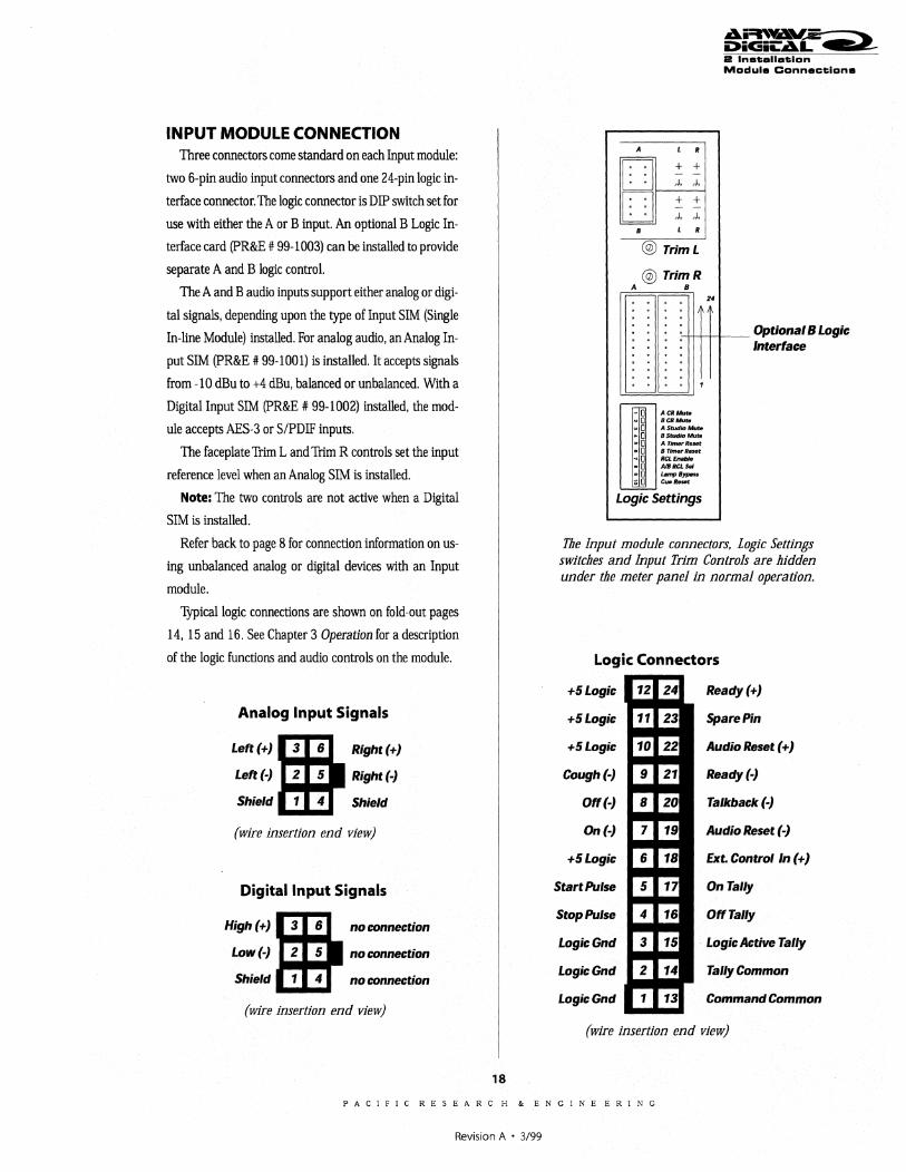
INPUT MODULE CONNECTION Three connectors come standard on each Input module:
two 6-pin audio input connectors and one 24-pin logic in
terface connector. The logic connector is DIP switch set for
use with either the A or B input. An optional B Logic In
terface card (pR&E # 99-1003) can be installed to provide
separate A and B logic controL
The A and B audio inputs support either analog or digi
tal Signals, depending upon the type of Input SIM (Single
In-line Module) installed. For analog audio, an Analog In
put SIM (PR&E # 99-1001) is installed. It accepts signals
from -10 dBu to +4 dBu, balanced or unbalanced. With a
Digital Input SIM (PR&E # 99-1002) installed, the mod
ule accepts AES-3 or S/PDIF inputs.
The faceplate Trim L and Trim R controls set the input
reference level when an Analog SIM is installed.
Note: The two controls are not active when a Digital
SIM is installed.
Refer back to page 8 for connection information on us
ing unbalanced analog or digital devices with an Input
module.
Typical logic connections are shown on fold-out pages
14, 15 and 16. See Chapter 3 Operation for a description
of the logic functions and audio controls on the module.
Analog Input Signals
Left (+) fi6 Right (+)
Left (-) 2 5 Right (-)
Shield 1 4 Shield
(wire insertion end view)
Digital Input Signals
High (+) fi6 no connection
Low (-) 2 5 no connection
Shield 1 4 no connection
(wire insertion end View)
18
A L •
D + + .. - -,J, ,J,
[J + + .. - -,J, ,J,
= • L • @ TrimL
@ TrimR A •
1
-=-" 0 ACRMute -0 BCRMute
" 0 A Studio Mute ·0 BStudioMute ·0 A Timer Reset
·0 B Timer Reset
"0 RCL Enable ·0 AlBRCLSeI -0 LsmpByp8$S ;;0 Cue Reset
Logic Settings
2.
Ai=nY.AV'~ ~iGii:'AL E! Inatallatlon Modula Connection a
Optional B Logic Interface
The Input module connectors, Logic Settings switches and Input Trim Controls are hidden under the meter panel in normal operation.
Logic Connectors
+5 Logic
+5 Logic
+5 Logic
Cough(-)
Off(-)
On(-)
+5 Logic
Start Pulse
Stop Pulse
LogicGnd
LogicGnd
LogicGnd
I 12
11
10
9
8
7
6
5
4
3
2
1
24
23
22
21
20
19
18
17
16
15
14
13
Ready(+)
Spare Pin
Audio Reset (+)
Ready(-)
Talkback (-)
Audio Reset (-)
Ext Control In (+)
On Tally
Off Tally
Logic Active Tally
Tally Common
Command Common
(wire insertion end view)
PACIFIC RESEARC H & ENGINE ERING
Revision A • 3/99
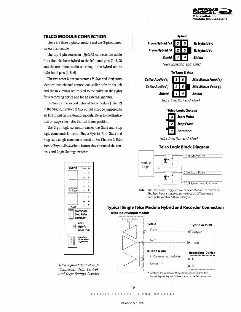
TELCO MODULE CONNECTION There are three 6-pin connectors and one 3-pin connec
tor on this module.
The top 6-pin connector (Hybrid) connects the audio
from the telephone hybrid to the left-hand pins (1, 2, 3)
and the mix-minus audio returning to the hybrid on the
right-hand pins (4, 5, 6).
The two other 6-pin connectors (To Tape and Aux) carry
identical two-channel connections (caller only on the left
and the mix-minus return feed to the caller on the right)
for a recording device and for an external monitor.
To monitor the second optional Telco module (Telco 2)
in the Studio, the Telco 2 Aux output must be jumpered to
an Ext. Input on the Monitor module. Refer to the illustra
tion on page 2 for Telco 2's mainframe position.
The 3-pin logic connector carries the Start and Stop
logic commands for controlling a Hybrid. Both Start and
Stop use a single common connection. See Chapter 3 Telco
Input/Output Module for a feature description of the con
trols and Logic Settings switches.
Hybrid From To
[J + + .. - -
'" '" IT] + + .. - -
'" '" = To Tape L R
[[J + + - -
'" '" L R Aux o Start Pulse : Stop Pulse
Common
From @Hybrid
Gain Trim
oo~-... 0 Timer Reset .0 Tape Feed ·0
Hybrid
Ai=nYA~=-:--~ :> DiGiL'AL' _ 2 Installation Module Connections
From Hybrid (+) Jl6 To Hybrid (+)
From Hybrid (-) 2 5 To Hybrid (-)
Shield 1 4 Shield
(wire insertion end view)
To Tape Br Aux
Caller Audio (+) Jl6 Mix-Minus Feed (+)
Caller Audio (-) 2 5 Mix-Minus Feed (-)
Shield 1 4 Shield
Module Logic
(wire insertion end View)
Telco Logic Output
~ Start Pulse
2 Stop Pulse
1 Common
(wire insertion end View)
Telco Logic Block Diagram
~~:HEI'31J91"'"PCI" I~~~~ __ -
Note: The Start Pulse is triggered by the Telco Module On command. The Stop Pulse is triggered by the Module Off command. Each pulse width is 220 ms in length.
>-~:~i _l_O_~_~_~a_el_I:_r~_oU_n~-,-y,_p_re __ f_a_de_r_) _}:;~;~;;~~~:;;; L..::J~_R....:.(H_O_S....:.t)~* ______ l. R !. ~ ;r
Telco Input/Output Module Connectors, Trim Control
and Logic Settings Switches l ... __ .. _____ . __ ................ ) ~.-----.... --.--.--.-------.---. .:
19
• Contains the caller Mix-Minus Feed, which follows the
Pgm-l, Pgm-2, Pgm-3,Offiine status of the Telco module.
PACIFIC RESEARC H & ENGINE ERING
Revision A • 3/99
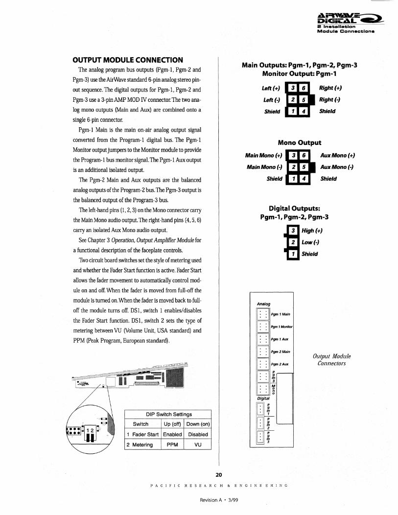
OUTPUT MODULE CONNECTION The analog program bus outputs (pgm-1, Pgm-2 and
Pgm-3) use the AirWave standard 6-pin analog stereo pin
out sequence. The digital outputs for Pgm-1, Pgm-2 and
Pgm-3 use a 3-pin AMP MOD IV connector. The two ana
log mono outputs (Main and Aux) are combined onto a
single 6-pin connector.
Pgm-1 Main is the main on-air analog output signal
converted from the Program-l digital bus. The Pgm-1
Monitor output jumpers to the Monitor module to provide
the Program-1 bus monitor signal. The Pgm-1 Aux output
is an additional isolated output.
The Pgm-2 Main and Aux outputs are the balanced
analog outputs of the Program-2 bus. The Pgm-3 output is
the balanced output of the Program-3 bus.
The left -hand pins (1, 2, 3) on the Mono connector cany
the Main Mono audio output.The right-hand pins (4,5,6)
cany an isolated Aux Mono audio output.
See Chapter 3 Operation, Output Amplifier Module for
a functional description of the faceplate controls.
Two circuit board switches set the style of metering used
and whether the Fader Start function is active. Fader Start
allows the fader movement to automatically control mod
ule on and off. When the fader is moved from full-off the
module is turned onWhen the fader is moved back to full
off the module turns off. DSl, switch 1 enables/disables
the Fader Start function. DSl, switch 2 sets the type of
metering between VU (Volume Unit, USA standard) and
PPM (peak Program, European standard).
DIP Switch Settings
Switch Up (off) Down (on)
Fader Start Enabled Disabled
2 Metering PPM VU
20
Ai~~;;;-=---" DiGi;:Ar=: > Ii! Inauallatllen Medula Conn.aUlon.
Main Outputs: Pgm-1, Pgm-2, Pgm-3 Monitor Output: Pgm-1
Left(+)
Left (-)
Shield
;.
6 Right(+)
2 5 Right(-)
1 4 Shield
Mono Output
Main Mono (+) ;'6 AuxMono (+)
Main Mono (-) 2 5 Aux Mono (-)
Shield 1 4 Shield
Digital Outputs: Pgm-1, Pgm-2, Pgm-3
~Hi9h(+)
2 Low(-)
1 Shield
Analog
~ : : Pgm 1 Main
~ 0' : Pgm 1 MDnilm' , ,
OpgmlAUX
0' : pgm 2 Main , ,
0' : Pgm2Au1C , ,
0' : 9,r--0' : Ai
, • 0
o Q 3
~DD~git~ , g , m
Dr+-: ~ '--
D~ , g , m
_3
Output Module Connectors
PACIFIC RESEARC H & ENGINE ERING
Revision A • 3/99
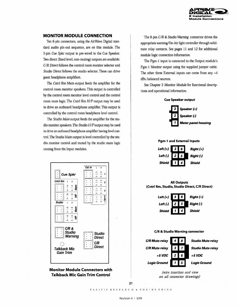
MONITOR MODULE CONNECTION Ten 6-pin connectors, using the AirWave Digital stan
dard audio pin-out sequence, are on this module. The
3-pin Cue Spkr output is pre-wired to the Cue Speaker.
Two direct (fixed level. non-muting) outputs are available:
CIR Direct follows the control room monitor selector and
Studio Direct follows the studio selector. These can drive
guest headphone amplifiers.
The Cntrl Rm Main output feeds the amplifier for the
control room monitor speakers. This output is controlled
by the control room monitor level control and the control
room mute logic. The Cntrl Rm HIP output may be used
to drive an outboard headphone amplifier. This output is
controlled by the control room headphone level control.
The Studio Main output feeds the amplifier for the stu
dio monitor speakers. The Studio HIP output may be used
to drive an outboard headphone amplifier having level con
trol. The Studio Main output is level controlled by the stu
dio monitor control and muted by the studio mute logic
coming from the Input modules.
DcueSPkr
CntrlRm L R
[] + + .S , , ,:;:~ J,
D + ±~ , , J, J,
Studio L R
[] + + .S .. ,:;:~ J,
D + ±~ ' .. J, J,
Do , CIR& , , Studio .. Warnmg
o Talkback Mic
Gain Trim
Ext In L R
[] + + . , - - 1 J, J,
B ± ± 2 .. J, J,
± ± 3 J, J,
D + + p , , - -fI, J, J, 1 =
[j' 0 Studio : : Direct
Do CIR : : Direct
Monitor Module Connectors with Talkback Mic Gain Trim Control
21
.a.i~VAV....ciOiGiiL.a.L > 2 Inaloallalolon Module Conneeloiona
The 8-pin CIR & Studio Warning connector drives the
appropriate warning/On-Air light controller through solid
state relay contacts. See pages 11 and 12 for additional
module logic connection information.
The Pgm-l input is connected to the Output module's
Pgm-l Monitor output using the supplied jumper cable.
The other three External inputs can come from any +4
dBu balanced sources.
See Chapter 3 Monitor Module for functional descrip
tions and operational information.
Cue Speaker output
~ Speaker (+)
2 Speaker (-)
1 Meter panel housing
Pgm-1 and External Inputs
Left (+) 116 Right (+)
Left (-) 2 5 Right (-)
Shield 1 4 Shield
All Outputs (Cntrl Rm, Studio, Studio Direct, C/R Direct)
Left(+) 116 Right(+)
Left (-) 2 5 Right (-)
Shield 1 4 Shield
C/R & Studio Warning connector
CIR Mute relay ..... - Studio Mute relay
CIR Mute relay Studio Mute relay
+SVDC +SVDC
Logic Ground _ .... Logic Ground
(wire insertion end view on all connector drawings)
PACIFIC RESEARC H & ENGINE ERING
Revision A • 3/99
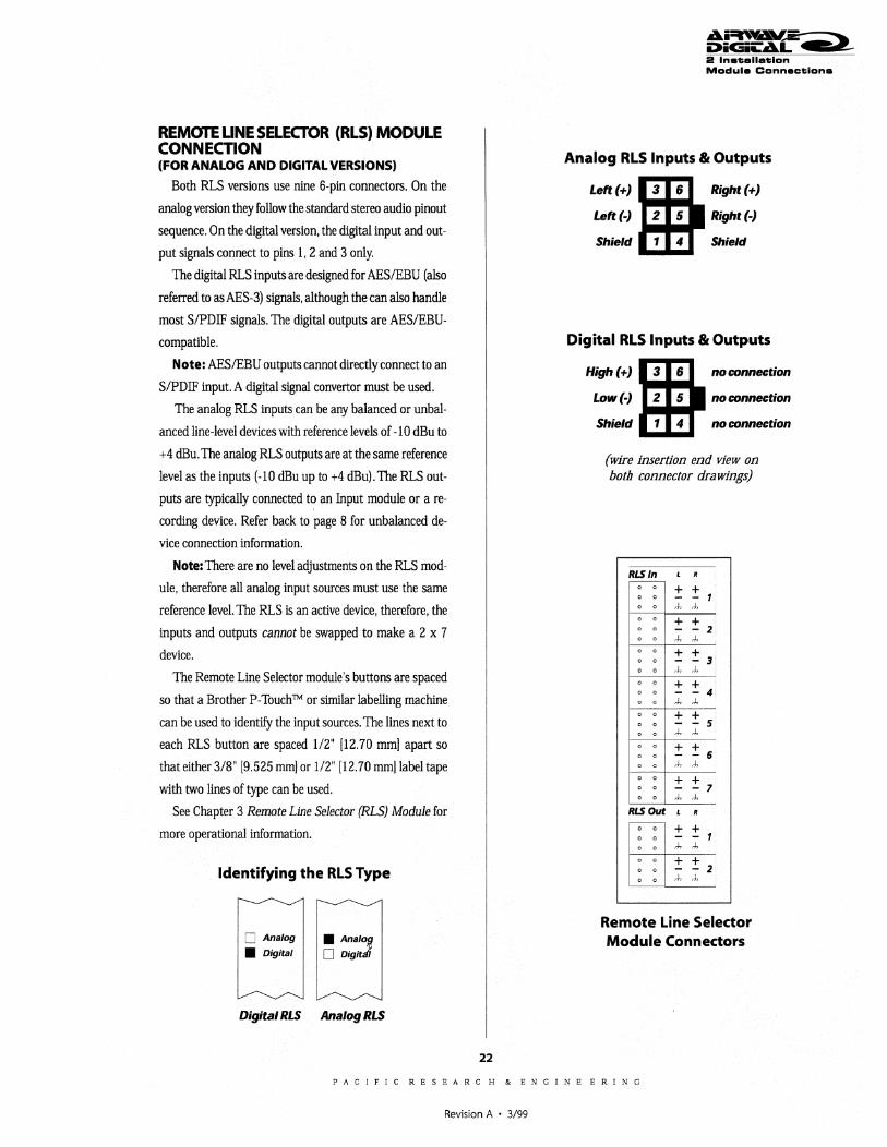
REMOTE UNE SELECTOR (RLS) MODULE CONNECTION (FOR ANALOG AND DIGITAL VERSIONS)
Both RLS versions use nine 6-pin connectors. On the
analog version they follow the standard stereo audio pinout
sequence. On the digital version, the digital input and out
put signals connect to pins 1,2 and 3 only.
The digital RLS inputs are designed for AESIEBU (also
referred to as AES-3) signals, although the can also handle
most S/PDIF signals. The digital outputs are AESIEBU
compatible.
Note: AESIEBU outputs cannot directly connect to an
S/PDIF input. A digital signal convertor must be used.
The analog RLS inputs can be any balanced or unbal
anced line-level devices with reference levels of -10 dBu to
+4 dBu. The analog RLS outputs are at the same reference
level as the inputs (-1O dBu up to +4 dBu). The RLS out
puts are typically connected to an Input module or a re
cording device. Refer back to page 8 for unbalanced de
vice connection information.
Note: There are no level adjustments on the RLS mod
ule, therefore all analog input sources must use the same
reference level. The RLS is an active device, therefore, the
inputs and outputs cannot be swapped to make a 2 x 7
device.
The Remote Line Selector module's buttons are spaced
so that a Brother P-Touch™ or similar labelling machine
can be used to identify the input sources. The lines next to
each RLS button are spaced 112" [12.70 mm] apart so
that either 3/8" [9.525 mm] or 112" [12.70 mm]label tape
with two lines of type can be used.
See Chapter 3 Remote Line Selector (RLS) Module for
more operational information.
Identifying the RLS Type
o Analog
• Digital • Analog o DigitJi
Digital RLS Analog RLS
22
.a.i=twav;-=----DiC5iiL.a.~ > Ii! Inat:anat:lon Module Conneot:lone
Analog RLS Inputs" Outputs
Left (+) 116 Right (+)
Left (-) 2 5 Right (-)
Shield ., 4 Shield
Digital RLS Inputs" Outputs
High(+) 116 no connection
Low (-) 2 5 no connection
Shield ., 4 no connection
(wire insertion end view on both connector drawings)
RLSln L R r-;-;;- + +
0 0 - - 1 0 0 ,), ,),
0 0 + + 0 0 - - 2i 0 0 ,), ,),
0 0 + + 3i 0 0 - -0 0 ,), ,),
0 0 + + ! 0 0 - - 4 0 0 ,), ,),
0 0 + + 0 0 - - 5' 0 0 ,), ,),
0 0 + + 0 0 - - 6 0 0 ,), ,),
0 0 + + 0 0 - - 7: 0 0 ,), ,),
RLSOUt L R
~ + + 0 0 - - 1 0 0 ,), ,),
0 0 + + ;
0 0 - 2 0 0 ,), ,),
Remote Line Selector Module Connectors
PACIFIC RESEARC H & ENGINE ERING
Revision A • 3/99
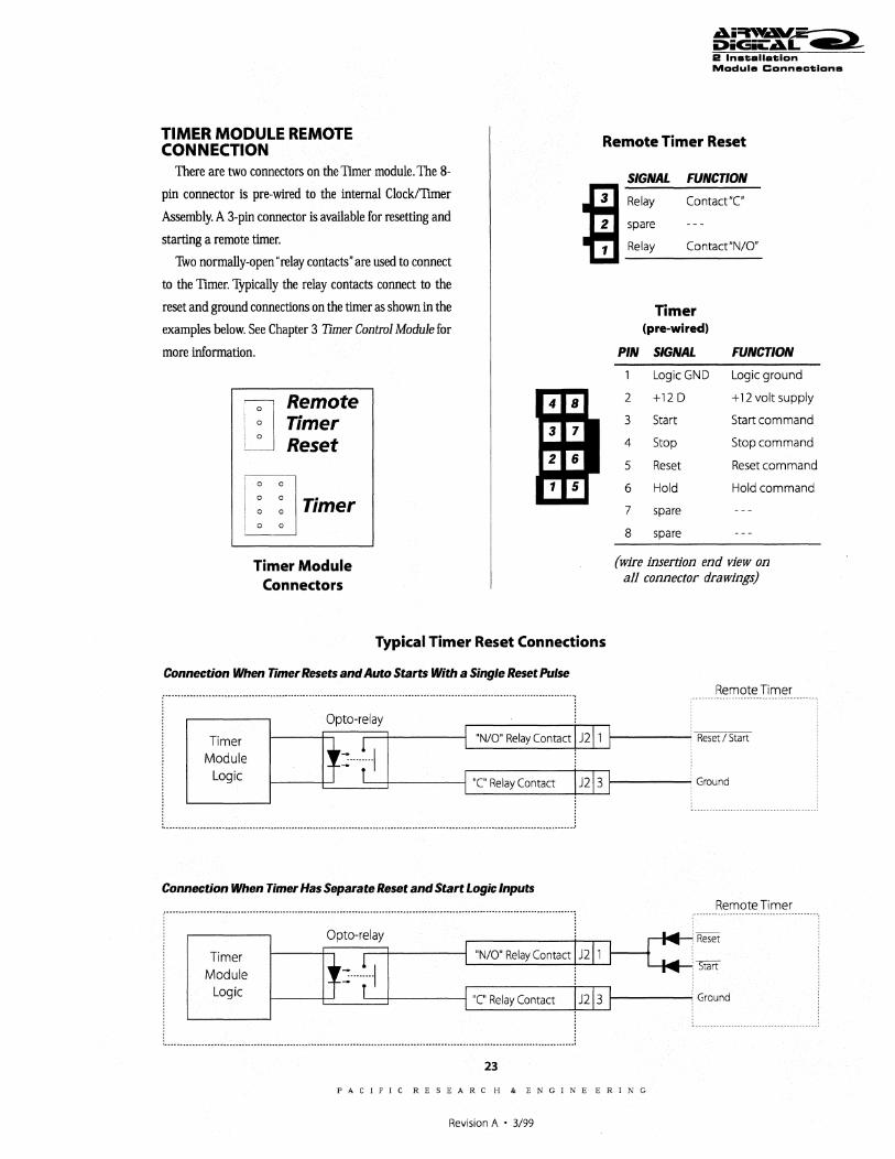
2 In.".lIa"lan Madule Cannee"lana
TIMER MODULE REMOTE CONNECTION
Remote Timer Reset
SIGNAL FUNCTION There are two connectors on the Timer module. The 8-
pin connector is pre-wired to the internal Clock/Timer
Assembly. A 3-pin connector is available for resetting and
starting a remote timer.
Two normally-open "relay contacts" are used to connect
to the Timer. Typically the relay contacts connect to the
reset and ground connections on the timer as shown in the
examples below. See Chapter 3 Timer Control Module for
more information.
~ 23,
I_R_e_la_Y __ c_o_n_ta_c_t_"C_"_ spare
Relay Contact"N/O"
]
•. a Remote . a Timer ! a Reset
TIJo
1 0 a •
I. a 0 Timer o 0
Timer Module Connectors
4 8
3 7
2 6
1 5
Typical Timer Reset Connections
Connection When Timer Resets and Auto Starts With a Single Reset Pulse
Opto-re ay
i "N/O" Relay Contact I J211 I Timer
l~r:""""i""1 Module Logic I "C" Relay Contact 1J213 i
Connection When Timer Has Separate Reset and Start Logic Inputs
.... ·._0··.--. __ ··· ......... ······ ... -._-- .... ··· ......... __ .. __ ..................... _ ....... _ .. ___ ..... _ .. _ ..................... ___ ... " . .
Timer
Module Logic
Opto-relay
"N/O" Relay Contact J2 : ........ 1
I---t::::~--===j----I "C" Relay Contact
. . ,-_ ...... _-_ ... __ .. _----.- ........ _ ......... _-- .. -....... _ ...... -................. -..... -........ - .. --_ ................. __ .............. .
23
Timer (pre-wired)
PIN SIGNAL FUNCTION
LogicGND Logic ground
2 +12 D + 12 volt supply
3 Start Start command
4 Stop Stop command
5 Reset Reset command
6 Hold Hold command
7 spare
8 spare
(wire insertion end view on all connector drawings)
Remote Timer
•
Reset / Start
Ground
Remote Timer
PACIFIC RESEARC H & ENGINE ERING
Revision A • 3/99
T operational function> 1m- each module
and component in the AirWave Digital console is
covered in this chapter.
Input Modules AirWave Digital has six types of input modules
available: Microphone Preamplifier. analog or
digital Input. Telco Input/Output and analog or
digital Remote Line Selector (RLS).
Any combination ofInput. Microphone Preamp
and RLS modules may be installed into the Input
module positions in the mainframe. Up to two
Telco modules can be installed in their dedicated
mainframe positions (immediately to the left of
the Monitor module). although any other Input
module can also be installed into these positions.
The RLS position (between the Monitor and Out
put modules) can only have an RLS or Microphone
Preamp module. or a tape remote or other cus
tom panel installed in its position.
MICROPHONE PREAMPLIFIER MODULE
The Microphone Preamplifier module amplifies
from one to five low-level microphone Signals to
line-level. The +4 dBu output of each preampli
fier can be jumpered directly to an Input module.
an analog RLS. routed to a patch bay or connected
to an external line-level Signal processor.
The module contains five high-performance
transformerless microphone preamplifiers with a
board-mounted DIP switch (DSl) for SWitching
phantom power to any input. In the illustration
inputs 2 and 4 are shown switched on.
Five faceplate-accessible gain trim controls set
the preamp gain as required for the application.
Multiple Microphone Preamplifier modules may
be used in the AirWave Digital mainframe.
o -'
-' ~ ... -
Microphone Inputs 1 - 5
Preamplifier Outputs 1 - 5 Mic signal paralleled to left and right outputs.
Trimpots for Inputs 1 - 5 Normally hidden behind a security cover, aJJows nominal microphone signal levels of -70 dBu to -30 dBu .
Phantom Power Selection
~---------'" ";:'[jLJC '-.
DS1 imlmllllmimil
PACIFIC RESEARCH 8< ENGINEERING
Revision A • 3/99
3 ap.r.~lan
ANALOG OR DIGITAL INPUT MODULE The Analog version controls preamplified microphones or analog line-level sources on both inputs. The digital
version controls AES-3 or S/PDIF digital sources on both inputs. Input modules can be reconfigured in the field
by changing the plug-in SIM card. The functional differences for the digital version are listed within brackets.
AlB Inputs Two balanced analog stereo linelevel inputs (A & B). [Two differential AES-3 compatible inputs on connector pins 1, 2, 3 only]
Logic Connector(s) Connects a mic remote control panel or a peripheral device for remote control of both the device and the module. Refer to the Input Module Connections Quick Reference (page 13 of the Installation chapter) for more information on the control functions. An optional B logic Interface can be added for separate logic control on each input.
AlB Input Selector Selects the active input (A or B). The button is lit when the B input is selected. Changing inputs while the module is On turns the module Off.
Off-Line When active (button lit), the pre-fader and pre-On/Off audio is sent to the Telco module s off-line telephone foldback bus.
Fader 100 mm level control. Set the fader to the reference line (-12 dB) to achieve 0 VU on the program output meters with a nominal +4 dBu analog input signal (and properly adjusted input level trimpots). [Set the control to nominal, -12 dB to provide unity gain of digital input signals]
Yellow Off Button Turns the module off. removing the module s audio from all program buses. May also turn off Cue and initiate the logic control commands Stop Pulse and Orf Tally following the logic Settings switch positions.
11 • • •• I
~- .~-.. 'CIr_ • A __
.. ---.. A __
· --.. MIII:LIiOI : ==Logic Settings
DAD *8 Input
o
o
2
Input Level Trimpots Individual gain adjustment of the module s left and right channels (post AlB selection). [Not active with a digital SIM installed]
Logic Settings switches Sets the module s logic control functions for the A and B inputs. When the B logic Interface is installed, the AlB RCl Set Switch is not active. Refer to the Input Module Connections Quick Reference (page 13 of the Installation chapter) for more information on the switch functions.
Pgm-1, Pgm-2, Pgm-3 Assigns the module to any combination of the Program 1, Program 2 and Program 3 buses. The buttons are lit when assigned to a bus.
Cue Sends the pre-fader audio to the console s Cue speaker and to the console operator s headphones. The button is lit while Cue is active.
Red On Button Turns the module on, applying the module s audio to the selected program buses. It may also initiate logic control commands Start Pulse, Timer Reset, On Tally, Cue Off and mute the control room or studio speakers (and turn on the appropriate warning lamp) following the logic Settings switch positions.
PACIFIC RESEARC H & ENGINE ERING
Revision A • 3/99
TELCO INPUT/OUTPUT MODULE
Ai=nYAV,iei>iGi&:'AL > 3 Operation
The optional Telco Input/Output module interfaces a telephone hybrid with the console. The module also
provides a host/caller recorder connection. One or two Telco modules may be installed.
Hybrid From connects the caller audio from the telephone hybrid and To sends the selected console mix-minus audio back to the hybrid.
Logic Output A Start Pulse and a Stop Pulse is available for hybrid control. Each is a solid-state relay tied to a single isolated common.
Logic Settings Cue and Timer. when set to the left. reset the Cue function and/or the Timer reset at module On. Tape Feed is only active when two Telco modules are installed. It sets how the other caller's voice gets mixed on this module's To Tape and Aux outputs. When set to the left, both callers are mixed together on the left channel When set to the right, the other caJ1er is mixed with the right channel mix-minus audio.
Pgm-1, Pgm-2, Pgm-3 When lit and the module is On, assigns the caJ1er audio to the Pgm-1, Pgm-2 or Pgm-3 buses and assigns the associated program mix-minus feed to the caJ1er. When two Telco modules are installed both wiJ1 have the same setting.
Cue When lit sends the pre-fader, pre-On/Off audio to the console-mounted Cue speaker and to the console operator's headphones.
Red On Button Turns the module On, applying the caller's audio to the selected program bus. The caller Feed is also switched to the selected Program bus mix-minus. When the Timer reset switch is set to the left, the timer is reset. When the Cue reset switch is set to the left, and the Cue is on, the Cue function for this module is turned ofi
From @Hyf>rld
GalnTrfm
Auto-O Feed
Telco
Pgm.70
pgm.zO
pgm.JO
Off··O Line
Cue 0
o
3
To Tape/Aux To Tape connects the caller audio to the left channel, and the mix-minus audio (either Off-line or the Pgm assignment mix-minus) to the right channel of a call recorder. These same Signals are available on the Aux connector. With two Telco modules instaJ1ed, the left-hand module's Aux output can be jumpered to an External In on the Monitor module for separate Telco 2 tape feed monitoring.
From Hybrid Gain Trim Sets the level of the incoming caller audio from the hybrid. Can be from -10 dBu up to +4 dBu.
Autofeed When lit, the module performs automatic switching as described under Telco Operation on the next page. When unlit, the return mix-minus feed is manually selected. When two Telco modules are installed both will have the same setting.
Off-Line When lit sends the Off-Line mix to the caJ1er. When two Telco modules are installed both will have the same setting.
Fader 100 mm level control. Set the fader at the reference line (-12 dB) to achieve 0 VU on the program output meters with a properly adjusted hjbrid input level.
Yellow Off Button Turns the module Off. removing the caller's audio from the selected program bus and changing the caJ1er Feed to the Off-Line bus when Autofeed is active. When the Cue reset switch is set to the left, and the Cue is on, the Cue function for this module is turned off.
PACIFIC RESEARC H & ENGINE ERING
Revision A • 3/99
TELCO OPERATION The first Telco module (Telco 1) is always in
stalled to the left side of the Monitor Module. A
second Telco module (Telco 2) can be installed next
toTelco l.
When two Telco modules are installed, the two
modules must track certain switch settings to en
sure the correct mix-minus is always sent back to
the two callers. Thus the Program bus select, Off
line select and Autofeed buttons on the two mod
ules are automatically linked together so that
changing any setting on either module affects both
modules.
There are two main operational modes for the
Telco module(s): Manual and Autofeed.
Manual Mode
The Autofeed button is unlit. Only one Feed
source can be selected (Off-Line, Pgm-l, Pgm-2,
Pgm-3).
When Off-Line is selected, the caller Feed is the
Off-Line mix bus regardless oftheTelco module's
onloff status. The caller is not assigned to any pro
gram bus, thus the caller does not go on-air if the
module is turned On (typically this would only be
done to activate the Start Pulse logic output at
module On).
When a Program bus is manually selected, the
caller Feed is that Pgm assignment's mix-minus,
regardless of the module's on! off status. If the mod
ule was already On, selecting the program bus adds
the caller voice to that bus. Turning the module
Off removes the caller from the program bus but
will not change the caller Feed.
Autofeed Mode
The red Autofeed button is lit. Anyone Pro
gram bus can be selected. When the module is
On, the caller Feed is that program bus
assignment's mix-minus.
4
Ai=nv.&.V'~ iOiGiiLAL -~ 30peretian
When the module is turned Off, the caller Feed
automatically changes to the Off-Line bus and the
Off-line button is lit. The selected Pgm button
winks to indicate the assigned program bus. If no
bus is yet assigned, the three Pgm buttons flash
together to indicate no bus is selected and the caller
will not go on-air when the module is turned on.
AirWave Digital Telco Module Configuration
Telco
With two Telco
modules.
o
:-1 10.
Telco 1
TalkbMkMh: GaInTrlm
:~Studio ; .. Direct
;=:gft8Ct I
.~. :~~ Monitor Telco-i
Talk Ba,k
~ .
MUL~
Studio
-.--:~ Pgm-I •• Pgm-2
Headphone
.... mJ...."
Monitor Module
PACIFIC RESEARCH & ENGINEERING
Revision A • 3/99
·i:::nYAV'~ ....... i>iGiL".L A 3 Operation
REMOTE LINE SELECTOR (RLS) MODULE - ANALOG OR DIGITAL VERSION Each RLS module version (stereo analog or AES-3 digital) contains two electronic switches which share seven
common inputs to create a pair of 7 x 2 switchers. The seven sources are independently selectable between the
two outputs. There are no signal level trim adjustments on this module. The functional differences of the digital
version are within the brackets.
RLS In The seven stereo line-level inputs. Inputs must be at equivalent reference input levels between -10 dBu and +4 dBu. [The seven AES-3 signals connect to pins 1, 2 and 3 only. There is no connection to pins 4, 5 and 6.]
RLS Type A Digital RLS is illustrated. The Analog box is filled for an Analog RLS.
Selector-2 The seven buttons select the input assigned to RLS Out 2. Only one button can be selected at a time.
D Analog
• Digital
~D ~D ~D ~D ~D ~D ~D
Selector-1
~D ~D ~D
n ~LJ
SeJector-2
o
5
RLS Out The line-level outputs from Selector-1 and Selector-2. The RLS is a unity gain device, thus the output reference level is equal to the selected input's reference level. [The two AES-3 signals are output on pins 1, 2 and 3 on each connector. There is no connection to pins 4, 5 and 6.]
Selector-1 The seven buttons select the input assigned to RLS Out 1. Only one button can be selected at a time.
PACIFIC RESEARCH & ENGINEERING
Revision A • 3/99
Output Module
Ai=nY~--;;.---"" ~iGiLAa:=: > 3 Operation
The Output module has the DACs (Digital-to-Analog Converters) for the analog signals (pgm-l, Pgm-2,
Pgm-3, Cue and Telco Mix-Minus) and the line output amplifiers for the three stereo analog Program buses
(Pgm-l, Pgm-2 and Pgm-3) and the two Mono outputs (Main and AUx). It also has the output drivers for the
three digital Program outputs. Operator selection of the Mono source and the right-hand meter is also on this
module.
Pgm-1 Main, Monitor, Aux Main is the onair analog Program 1 balanced stereo output. The Monitor output is jumpered, using the supplied cable, to the Monitor module. The Aux output is a resistively-isolated output.
Mono The Main Mono output (pins 1, 2, 3) and a resistively-isolated Auxiliary Mono output (pins 4, 5, 6) are on a single connector. Both are analog outputs.
Pgm-1, Pgm-2, Pgm-3 The differential {transformer-coupled} AESIEBU digital outputs for the three program buses.
Cue A momentary button to route the Cue bus to the right-hand level meters, overriding the Pgm-2 or Pgm-3level indication while the button is held.
pgm·'D pgm.2D pgm.3D
Monaural Analog Output
Dpgm-2D *Pgm.3
Meter Select
o
6
Pgm-2 Main and Aux, Pgm-3 Main The analog outputs {balanced stereo} of the Program-2 and Program-3 buses.
Meter Panel Latch opening.
Pgm-1, Pgm-2, Pgm-3 Selects the monaural analog output source. Only one source (program-1, Program-2 or Program-3) can be selected. The selected analog stereo source is then resistivelysummed to mono before being amplified for the active balanced Mono outputs.
Pgm-2/Pgm-3 Meter Select When lit indicates that the right-hand meter is displaying the Program-3 output levels. When unlit indicates the right-hand meters are displaying the Program-2 output levels.
PACIFIC RESEARCH & ENGINEERING
Revision A • 3/99
Monitor Module
Ai=l\VAV ...... =--=---ii>iGiiLAL > 3 Dperetion
The Monitor module contains the monitor source selectors, monitor control and Talkback facilities for the
control room and one studio.
Cue Spkr CuelTalk bus amplifier output. Prewired to the meter panel Cue Speaker.
Cntrl Rm The Control Room volume controlled outputs. Main connects to an external amplifier for the Control Room speakers. HIP connects to an external headphone amplifier.
C/R & Studio Warning logiC output to the Control Room and Studio warning light inteIfaces.
TalkbackMicGain Trim Sets the level of the Talkback mic into the studio outputs.
Talkback Mic Allows communication to the studio while the TaIkback button is pressed.
Monitor Controls the level of the Studio Main output.
Talkback Sends the Talkback mic to the Studio Main and HIP outputs while pressed.
Cue Controls the level of the Cue Splcr output .
Headphone Controls the volume of the headphone audio sent to the headphonejack and to the CntrI Rm HIP output.
Monitor Controls the volume of the Cntrl Rm Main output
Headphone Jack Low- or high-impedance stereo headphones can be plugged into this jack. To prevent headphone or hearing damage, always turn the Headphone control fully counterclockwise before plugging in headphones.
Extln 1 I
D· : ± ±1 • • ,J, '" 8': 2:2:, • , ,J,,J,
· . + + • • ~ ~ 3
D:; ;~P · . ,J,:i If
: : Studio D' , C/R&
, , Warning 8' , Studio : : Direct
o Talkback Mit
Gain Trim
• 00 0 Monitor
I Talk I Back
• 00 0 CUe
• 00 D Headphone
~ • 00 D Monitor
<Q> Headphone
D' C/R : : Direct
_D _D _D
pgm.ID pgm.2D pgm.3D TelcoD
Mix
Studio
_D _D _D
pgm.ID pgm-2D
pgm.3D TeicoD
Mix
Control Room
o o
7
Ext In External line level inputs that feed the top three buttons on each Source Selector. The Pgm-l input comes from the Output module, using the supplied cable, to feed the Pgm-l monitor selector button.
Studio The selected outputs from the Studio Monitor Source Selector. Main connects to an external amplifier for the Studio monitor speakers. HIP connects to an external headphone amplifier for the Studio headphones.
Studio Direct Fixed volume output of the Studio Source Selector. Note that Talkback is not in this output. C/R Direct Fixed volume output of the Control Room Monitor Source Selector.
Studio Monitor Source Selector Selects the audio sent to the Studio outputs from the three external audio inputs, Pgm-l, Pgm-2, Pgm-3 and the Telco 1 Mix (which is the Telco 1 s mix-minus on one channel with the Telco 1 caller on the other channel) . Multiple sources can be selected for simultaneous monitoring.
C/R Monitor Source Selector Selects the audio for the control room outputs and the headphone jack from the three external audio inputs, Pgm-l, Pgm-2, Pgm-3 and the Telco 1 Mix (which is the Telco 1 s mixminus on one channel with the Telco 1 caller on the other channel). Multiple sources can be selected for simultaneous monitoring.
PACIFIC RESEARC H & ENGINE ERING
Revision A • 3/99
Timer Control Module
.4i=nY4.V~·==--'" i:)iGii:'AL > 3 Oparat:lan
The Timer Control module is pre-wired to the Clock/Timer assembly in the meter panel. The Timer can be
manually controlled using the Timer Control module buttons. When the Auto function is active the Timer is
automatically controlled through the Timer reset control logic from the Input modules.
Remote Timer Reset Logic output to reset a remote timer.
Meter Panel Latch opening.
Reset Resets the timer to 00:00.00. If the timer was already counting, the timer wm then continue to count up from 00:00.00. Reset pressed while the timer is stopped simply returns the time display to 00:00.00.
Start Immediately starts the timer from the displayed time.
[IJ Remote • Timer o Reset
DO: Timer ..
Auto 0
Reset 0 Hold 0 stanD Stop 0
o
8
Timer Supplies power and logic control to the clock/timer.
Auto When Active {lit}, the timer automatically resets to 00:00.00 and immediately starts counting whenever an Input module, with its timer reset function enabled, is turned On. When the Auto button is not lit, the timer is disabled from automatic Input module control.
Hold When pressed and held, stops the timer s display to show the elapsed time as the timer continues to run. Releasing Hold jumps the time display to the current run time.
Stop Immediately stops the timer, leaving the stopped time displayed.
PACIFIC RESEARC H & ENGINE ERING
Revision A • 3/99
Meter Panel
Ai=nv...LL»iGiiLA~ 3 Operation
The meter panel holds the ClockiTimerassembly, the two sets of bar graph level meters and the Cue/Talkback
speaker. The clock has no external controls. Clock time setting requires the use of the Clock Setting Magnet Tool
(supplied in the Tool Kit) when the clock is set for master mode. In slave mode, where clock timing is derived from
an ESE time code signal, the clock does not need to be set. See the section in Chapter 2, Installation, Setting the
Clock, for information on setting the time.
• PACIFIC RESEARCH. ENGINEERING
Meter Panel Components
Clock Display Cue/Talkback Speaker
Pgm-l Level Meters
pgm-2 or pgm-3 Level Meters
The electronic meter movements have no individual meter calibrations or alignments. The meters use IEEE
standard 152-1991 (standard audio program level measurement). When set for PPM display mode, via the
Output module DIP switch, the PPM indications will light and a +4 dBu sine wave output signal will display at
-8 on the PPM scale. When set for displaying VU, the VU indications will light and a +4 dBu sine wave output will
display at 0 on the VU scale. Each of these settings corresponds to -20 dBFS (decibels below Full Scale digital
output).
The meters display the left channel audio output on the top row and the right channel audio on the bottom row
of each meter. The right hand meter can momentarily show the Cue bus level by pressing the Cue button on the
Output module. While this button is pressed the top row of LEDs show the Cue bus output level.
The Cue/Talkback speaker's impedance is 45 ohms with a 3-watt power-handling capacity. The speaker vol
ume is controlled by the Cue volume control on the Monitor module. A 3-watt amplifier IC on the Monitor
module drives the speaker. Refer to Chapter 5, Maintenance & Alignment, Meter Panel Assemblyfor speaker replace
ment procedures.
9
PACIFIC RESEARCH & ENGINEERING
Revision A • 3/99
L chapter has technkal descriptions of
the mainframe. each AirWave Digital module. the
clock/timer assembly and the power supply.
MAINFRAME The AirWave Digital mainframe consists of a
welded all-steel bottom chassis with a hinged
overbridge-style meter panel. The modules' metal
faceplates complete the mainframe enclosure by
fastening to the chassis through a knurled captive
fastener at the top of the faceplate and a hex-head
faceplate screw at the bottom.
Each circuit board has one keyed 96-pin gold
plated Euroconnector that plugs into the mother
board from the top. The motherboard consists of
two connectorized sections in the AirWave Digi
tal-12 and three sections in the AirWave Digital-
20. The motherboard sections fasten to formed
metal supports on the bottom of the chassis. The
steel motherboard supports run the width of the
mainframe for rigidity.
To ensure high RFI shielding. all wiring shields
ground directly to the chassis through the face
plate and knurled fastener right at the input con
nectors. A ground screw near the DC power cable
entry point ties the mainframe chassis to the tech
nical ground reference.
The ten-foot DC power cable is soldered to the
right end of the right-hand motherboard section.
A keyed connector fastens the power cable to the
rack-mount AirWave Universal Power Supply.
MICROPHONE PREAMP MODULE For this section refer to the three Microphone
Preamplifier module schematic pages (92-961) in
Chapter 6.
Each of the five balanced microphone inputs
feed a SSM2017. a precision surface-mount mi
crophone preamplifier IC. It unbalances and am
plifies the mic Signals up to -10 dEu. The preamp
ICs are protected against Switching transients and
DC voltage surges by the Zener diodes. resistors
and coupling capacitors found between the input
connector and the preamp IC.
DIP switch DS 1 has five switches to tum phan
tom power on or off to the five mic inputs. The
switches ship from the factory set in the off posi
tion. Only those individual inputs that are power
ing condenser microphones should be set for phan
tom power on. The +45 volts is then coupled to
the inputs via a pair of 6.81 k resistors.
Faceplate-accessible trimpots (RVI - RV5) set
the preamp gain for a nominal output signal level
of +4 dBu.
TPI -TP5 allow the internal nominal-lO dBu
signal level to be monitored. Dual OP275 opamps
boost and differentially balance the -10 dBu sig
nals to +4 dBu at the mic preamp output.
6-pin output connectors simplify connection to
Input modules. paralleling the left and right chan
nels.
Polyswitch resettable fuses. Fl and F2. protect
against board component short circuits. Once the
over-current is removed. the fuses automatically
reset. Test point TP6 is the -16 VDC check point.
TP9 is the + 16VDC check point. TP8 is the phan
tom supply check point. The ground reference test
point is TP7.
PACIFIC RESEARC H & ENGINE ERING
Revision A • 3/99
INPUT MODULE For this section refer to the two Input Module
schematic pages (drawings 92-1004) and to the
two SIM schematic pages (drawings 92-1001 and
92-1002) in Chapter 6.
AnalogSIM
The two identical balanced inputs (A and B)
connect directly to the SIM socket. With an Ana
log SIM (99-1001) installed. the stereo audio sig
nals are unbalanced and amplified by OP275 dual
differential opamps on the SIM card. Four single
pole Single-throw (SPST) solid-state analog
switches toggle between the two inputs according
to the faceplate A/B button selection.
The selected stereo input is then routed through
trimpots R59 and R60 (Trim R and Trim L). The
outputs of the trimpots go through buffer/ampli
fier U 4 before being converted into digital signals
by U5. a Single chip ADC (Analog-to-Digital Con
verter). The ADC chip output (SDATA_SIM) is
routed back to the Input PCA through the SIM
socket.
DigitalSIM
With a Digital SIM installed (99-1002), the
AES/EBU input is coupled to an AES/EBU Re
ceiver (U2) through an isolating transformer (T 1)
and the A/B selection relay (K 1) .
U2 converts the incoming AES/EBU signal into
a serial data signal (SDATA) with a separate left!
right clock (FSYNC) and serial clock (SCLK). In
normal operation. the SDATA signal is routed
through an Asynchronous SRC (Sample Rate Con
verter). U4. to synchronize the incoming digital
audio with the DSP (via the FS64 clock). The out
put. SRC_DATA is then routed back to the Input
module through the SIM socket as SDATA.
The SRC can be bypassed by physically
jumpering El to E2. This switches which section
of U 1 is active. Normally the odd pins couple the
2
Ai=iwa.t:;;-:---... ilIiGi;:'A~ > 4 Equlpmenc Ceecrlptslon
signals through to the output while the even pins
are in a tri-state mode (at a high impedance). With
El jumpered to E2. the IDCSDATA from AES/
EBU receiver U2 is connected directly to the In
put module via the even pins of U I, while the odd
pins are at a high impedance.
If valid digital audio is not received. or if there
are excessive errors (e.g .. loss of lock, parity er
rors. biphase encoding violation). an ERF (Error
Flag) signal is sent back to the Input module where
a NOR gate in U15 mutes the SDATA signal.
Input Module
Every Input module fader gets its reference volt
ages (both High and Low) from the DSP. Each
fader's wiper output connects via a separate line
to the DSP for individual channel level control.
The faceplate assignment switches (A/B select.
bus assignment. Cue. Off-Line) are all on a Single
universal switch SIM. Each is a momentary SPST
switch with an integral LED indicator. The
switches connect directly to the gate array chip
(FPGA. U14) while the LEDs on the switches are
controlled by the FPGA through FET switches Q 1
- Q4, Q13 and Q14.
The module's On/Off switches mount on a sub
assembly (PR&E # 95-969-1). Each switch is a
momentary SPST with incandescent lamps con
trolled by the FPGA through FETs Q5 - Q 12 and
Q 15. The FETs not only turn the lamps on or off,
they also generate an AC-like voltage to increase
lamp life over normal DC powering.
When the Cue or Off-Line function is active. pre
fader controlled audio is applied to the appropri
ate summing bus. When any Program select but
ton is active. fader-controlled audio for that chan
nel is then connected to the selected digital Pro
gram bus.
The ten-position Logic Settings DIP switch
(DS 1) is used to tell the FPGA whether logic con
trol is to be active on the A or B input along with
PACIFIC RESEARC H & ENGINE BRING
Revision A • 3/99
what type of logic signals to use. Either the A or
the B input can be selected to use the logic control
features in the standard module. With the optional
B Logic Interface (PR&E # 99-1003) installed,
each input has its own logic control.
There are five logic control outputs and six logic
control inputs on each logic interface (92-1004,
page 2 of 2). All control inputs (U8 - U13) and
outputs (Ul - U5) are optically coupled for isola
tion and to prevent ground loops. The control in
puts are also current limited by U16 - U21 (LM317
regulators) so that any external logic level, from
+5 to +40 VDC, can be accommodated.
Polyswitch resettable fuses, Fl - F4, protect the
+12, +5, -16 and +16VDC supply against short
circuit damage by board problems. TP I, TP2, TP3
and TP4 are available for checking the +12, +5,
+ 16 and -16 volt supplies after the poly fuses.
TELCO INPUT/OUTPUT MODULE Refer to the two Telco Input/Output Module
schematic pages (92-1005) in Chapter 6.
The Telco Input/Output module is an optional
module. Up to two of the modules can be installed
into one mainframe in dedicated positions next to
the Monitor module.
A Single Telco module must be installed in the
first position to the left of the Monitor module. A
second Telco module can be installed next to the
first Telco module. This position automatically con
figures the second module as "Caller 2," while the
first Telco module remains as "Caller I."
Each Telco module handles interfacing one tele
phone hybrid. All of the caller mix-minus audio
control and caller audio program assignment is
built into the module.
The balanced From Hybrid input (shown on
page 1 of the schematic) is unbalanced and gain
controlled through the two halves of opamp U1.
The hybrid input gain is set by faceplate trim pot,
RVI (FROM HYBRID GAINTRIM).
3
Ai=n~--:;...--"" DiGiLA~ > 4 Equipment: Ceecript:ion
The output of the second half of the opamp con
nects to: U15 (an ADC, Analog-to-Digital Con
verter), to the left channel of the To Tape and Aux
outputs (through buffer/balancing opamps U2, U9
and U 1 0), and is coupled through the motherboard
to the other Telco module (as CALLER_OUT).
The ADC, U15, outputs digital data (SDATA)
to the DSP through the motherboard connector.
The digital audio data is handled as in the Input
modules, being converted back into analog on the
Output module as required for the Cue, mix-mi
nus and analog program outputs.
The fader, like those on the Input modules, also
connects directly to the DSP board, controlling
the audio level in the digital domain.
The output assignment switchboard plugs into
a SIM socket (see page 2 of the schematic). Each
assignment switch is a momentary type with an
LED indicator driven by FETs QlO - Q15. The
module On and Off switch assembly plugs into
the main PCA. The two switches are momentary
SPST with incandescent lamp illumination driven
by FETs Q1 - Q9.
The To Hybrid audio output (U3, U13, U14)
carries a sum of the Telco mix-minus (TEL1_MM)
and the caller's audio from the other Telco mod
ule (CALLER_IN), if one is installed.
TheTelco mix-minus audio (TELl_MM) comes
from a DAC (Digital-to-Analog Converter) on the
Output module. It is buffered by one-half of opamp
U3 on the Telco module. In addition to going to
the To Hybrid output, TELl_MM also goes to the
right channel Tape/ Aux output through U2, U 11
and U12.
The CALLER_IN audio (from the other Telco
module) may also be summed with TEL LMM
follOWing the setting of a DIP switch. The DIP
switch controls whether U 5 switches CALLER_IN
to the left or to the right channel of the Tape/ Auxl
Monitor outputs.
PACIFIC RESEARC H & ENGINE ERING
Revision A • 3/99
Tape I Aux Outputs
With one Telco module installed, the left chan
nel output is just the caller. The right channel out
put is the caller mix-minus audio (TELl_MM),
which is either the assigned program mix-minus
(when a Pgm button is assigned on the module)
or the Off-line mix audio (when Off-line is as
signed). Typically, only the talent's voice is assigned
to the Off-Line mix while recording callers off-air.
With two Telco modules installed. the Tape Feed
switch (DS 1, switch 3) becomes active. This switch
sets how the caller audio from the other Telco
module gets mixed into the Tape and Aux outputs
on that module.
When the Tape Feed switch is set to the left.
both callers are mixed together onto the left chan
nel. When it is set to the right, the other caller gets
mixed with the mix-minus audio (TEL1_MM) on
the right channel.
Monitoring Caller 2
Caller 2 can be monitored through the Cue bus
or through the Telco 1 Mix. To monitor Caller 2
separately from Caller 1 in the Studio requires that
an audio jumper be connected from the Aux out
put of the second Telco module to an External
Input on the Monitor module.
Auto-Feed
When the Auto-Feed function is active, the mod
ule status (On or Oft) affects the mix-minus switch
ing. When the module is On, the selected Program
mix-minus output is automatically sent to the
caller. When the module is turned Off, the Off-line
bus audio is automatically switched to the caller.
When Auto-Feed is not active, the selected
source (Pgm-l, Pgm-2, Pgm-3 or Off-line) is sent
to the caller when the module is both On and Off.
Note:With Off-Line manually selected, the caller
will not go on-air when the Telco module is turned
On since there is no Program bus assignment.
4
Ai=n~=-:---"" ii:»iGii:'AL\ > 4 Equipment Description
A front panel DIP switch sets cue, timer and
record output options. When the Cue Reset switch
is set to the right. the Cue function is turned off
when the Telco module is turned On or Off. When
the Timer Reset switch is set to the right, Telco
module On resets the Timer.
The Tape Feed switch is only active when two
Telco modules are installed. When set to the left.
the CALLER_IN audio (from the other Telco mod
ule) is mixed with the module'S caller audio on
the left To Tape output. When set to the right, the
audio from the other Telco module is mixed with
the mix-minus audio (TELl_MM) on the rightTo
Tape output.
Polyswitch resettable fuses, F1, F2, F3 and F4,
are used on the +12, +16, -16 and +5 VDC con
nections to protect against short circuit damage.
TP4 (-16 volts), TP5 (+5 volts) and TP8 (+16
volts) allow the voltages to be checked after the
fuses.
MOTHERBOARD Two motherboard sections are used in the Air
Wave-12, while three are used in the AirWave-20.
Each motherboard fastens to the bottom of the
mainframe and plugs together using a Mother
board Interconnect jumper (95-974). The power
supply cable is hard-wired to the right-hand
motherboard section (schematic 92-1009).
DSPBOARDS Two DSP (Digital Signal Processing) boards are
used in the AirWave-12, while three are used in
the AirWave-20. Each board plugs into the mother
board at a right angle from the modules and are
fastened to the mainframe's inside rear frame.
There are no adjustments or controls on the DSP
boards. Refer to the Motherboard schematics (92-
1007, 92-1008 and 92-1009) in the follOWing dis
cussion. Because of the proprietary nature of the
DSP boards, a schematic is not included.
PACIFIC RESEARC H & ENGINE ERING
Revision A • 3/99
The DSP is based on Motorola's 24-bit fixed
point DSP integrated circuits. 24-bit data words
provide 144 dB of dynamic range. The DSP oper
ates at a nominal sample rate of 48 kHz with on
board crystal synchronization. The internal reso
lution of 56-bits provides 336 dB of computational
dynamic range.
Two DSP options are available from the factory:
44.1 kHz internal sampling and/or external AES-
11 reference.
The left hand DSP card (DSP 1) connects to
the first eight Input module positions (see 92-1007,
P 12 for its connector pin-out) on both the AWD-
12 and the AWD-20. Each of the first eight Input
module positions connect their SDATA outputs,
along with their switch outputs and fader wiper
voltage, directly to the DSP board. When the Fader
Start Logic option is enabled on the Output mod
ule, a control signal from the DSP (FADER_ON)
is used to tum on the module as the fader is moved
from its full off position.
On the AWD-20, the next eight channels (in
puts 9 - 16) connect to DSP 2, identical to DSP 1
except for its EPROM.
The right-hand DSP (DSP 3) handles the re
maining four Input module positions for each size
console and the two Telco positions (which may
alternately have Input modules installed). This
DSP also creates the main digital output
(MIX_SDATA) and the meter outputs (DISPLAY
SERIAL DATA 1 and 2). See schematic 92-1009,
P12 for pin out information for DSP 3.
Each DSP board is linked to the other(s) via a
6-conductor flex cable on the motherboard. Each
board generates its own DSP Go and Fader High
and Low reference Signals. DSP 1 generates the
system clocks and system reset signals.
OUTPUT MODULE Refer to the six Output Amplifier module sche
matic pages (92-1006) in Chapter 6.
5
4i=t\YAV:--;;...---i:)iGii:'4~ > 4 Equipment Ceecrlptian
The right-hand DSP board outputs the
MIX_SDATA digital data stream to the Output
module FPGA (U9). The FPGA (see 92-1006, page
6 of 6) divides the individual data streams carried
within the multiplexed data to form the cue and
off-line buses (CUE/TEL_ STRMB) , and the three
individual program buses (PGM1_STRMB,
PGM2_STRMB, PGM3_ STRMB) from this mul
tiplexed input.
The various Program 1 outputs are on 92-1006,
page 1 of 6. The PGM I_STRMB (from the FPGA)
drives U22, an AES/EBU transmitter, and U25, a
DAC (Digital-to-Analog Converter).
The AES/EB U chip converts the serial data into
an AES-3 compatible Signal that is transformer
(Tl) coupled to the Pgm-l digital output. There
are no level adjustments on the digital outputs.
The DAC's left and right outputs are capaci
tively-coupled to the two buffers in Ul. Output
trim controls, RV2 and RV3, set the output level
of the right and left channels, respectively, for a
nominal +4 dBu. Output amplifiers U6, U7, U8
and UlO create the balanced Main and Aux out
puts. The Aux output is resistor-isolated from the
Main output. The Pgm-l Monitor output is con
nected (via the supplied patch cord) to the Pgm-1
monitor selector input on the Monitor module.
The Program 2 output is on page 2 of the sche
matic. It is identical to the Program 1 output with
out the additional Monitor output (the monitor
ing connection is done via the motherboard to the
Monitor module).
The Program 3 output is on page 3 of the sche
matic. It is identical to the Program 2 output, ex
cept it does not have an Aux output.
The two Mono outputs (Main and Aux) are se
lected from among the three program buses by
U36, a three-input analog switch. The left and right
channel inputs come from the DAC buffer outputs
on each program amplifier. U36 is controlled by
the three faceplate program select switches. The
PACIFIC RESEARC H & ENGINE ERING
Revision A • 3/99
switches are on a SIM card that plug into the SIM
socket (on page 5 of the schematic).
The output of U36 (an analog switch) is buff
ered and trimmed by U5 and balanced by U19
and U21 to create the Main Mono output. RVI
sets the output level to +4 dBu. The Aux Mono
output is resistor-isolated from the Main output.
A DAC (U28) converts the CUE/TEL_STRMB
output from the FPGA into the analog Cue and
Telco mix-minus signals. Both halves ofU4 buffer
these signals. The Cue signal goes to the Monitor
module while the Telco mix-minus signal goes to
the Telco module(s).
The Output module also has a board-mounted
DIP switch (DSl) that sets whether the global
Fader Start Enable function is on or off and
whether the meters display VU or PPM.
Four polyswitch resettable fuses (F 1 , F2, F3 and
F4) protect the supply against short circuit dam
age. TP9, TPlO, TP 12 andTP 16 are used to check
the +16, -16, +5 and +12 volt supplies, respec
tively.
MONITOR MODULE The Monitor module is a double-width module
with two independent circuit boards plugging into
two motherboard positions. Refer to the nine Moni
tor module schematic pages (four pages for 92-
964, five pages for 92-965) found in Chapter 6.
The left hand circuit board is the Monitor 1
board (92-964 schematic). It contains the moni
tor controls (Cue, Monitor, Headphone levels) for
the Control Room, the Talkback to the Studio mic
and control circuits, and the master level control
for the Studio monitor speakers.
The right hand circuit board is the Monitor 2
board (92-965 schematic). It is the same circuit
board as in the Analog Remote Line Selector mod
ule. When used as a Monitor 2 board, a different
FPGA chip is installed and several additional parts
6
Ai=l'VAV...iS'" = iDiGii:'AL _ > 4 Equipment D.ecription
are stuffed into the board for logic control of the
Monitor module. A complete circuit description
for this board is found later in this section under
Remote line Selectors.
The Monitor 1 board is divided between the
Control Room functions and the Studio functions.
Control Room Functions
The CR Select Input comes from the Monitor 2
board seven-button Control Room monitor source
selector. Being a balanced signal, the left and right
channels are unbalanced by the two halves of
opamp Ul and capacitively coupled to both the
CR Monitor Pot and to the CR headphone signal
assignment switcher U8.
The output of the CR monitor pot goes through
mute switch U5 (controlled by the CR Mute logic
bus) before being buffered and balanced for out
put by U2 and U3. This creates the main CR Moni
tor Output.
Studio Functions
The Studio Select Input comes from the Moni
tor 2 board seven-button Studio monitor source
selector. The balanced signals are unbalanced by
opamp U9 and capacitively coupled to both the
Studio Monitor Pot and to the Talent headphone
circuit (switcher U39 and opamps U 15 and U 16).
Talkback is inserted into the studio monitor sig
nal by UlO under control of the STTalkback com
mand. Ull and U12 amplify and balance the sig
nal for the ST Monitor Output.
Cue/Talkback
The Cue/Talkback audio is summed by one-half
of opamp U4 and capacitively coupled to the Cue
pot and to the headphone Signal assignment
switcher. The output of the Cue pot connects to
the Cue speaker amplifier IC (U23) which is muted
by Ql. Ql is controlled by the Cue Mute logic sig
nal that comes from U35 (Monitor 2 FPGA).
PACIFIC RESEARC H & ENGINE ERING
Revision A • 3/99
A built-in electret Talkback microphone is am
plified and buffered by opamp U13.Trimpot (RVl)
sets the mic volume for the monitor and head
phone feed. The Talkback mic audio is switched
into the Studio Monitor Output and the Talent H/
P audio by switcher ICs U 1 0 and U39 in response
to the Talkback button being depressed and held.
CR Headphone
The CR headphone audio is either the selected
source monitor or the Cue/Talk bus. When the
Cue/Talk logic signal (from U35, the Monitor 2
FPGA) goes high, the monitor audio is cut off and
Cue/Talk audio is fed to the console headphones.
The CR Headphone Level control sets the level to
the headphone amplifier U22 (for the module
headphone jack) and to the balanced CR Head
phone Output driver circuit (opamps U7 and U 14).
Polyswitch resettable fuses, F1, F2 and F3, are
used on the + 5, + 16 and -16 VDC connections to
protect against short circuit damage. TP3, TP8
and TP9 can be used to check the +5, -16 and
+ 16 volt supplies, respectively.
REMOTE LINE SELECTORS (RLS) There are two RLS modules available: Analog
and Digital. Refer to the Analog RLS schematic
(92-965, four pages) and the Digital RLS (92-
1012, two pages) in Chapter 6.
Analog RLS
The Analog RLS has seven line-level buffering
and switching circuits with two outputs in a 7 x 2
matrix. The line-level Signals (RLS 1 - RLS 7) are
AC coupled into the module. Opamps (U 1 - U7)
unbalance the left and right Signals, which are ca
pacitively coupled to the solid-state assignment
switches (U20 - U33). Pressing a front panel Ext.
1 - 7 button routes the External input audio
through the switches to Ul1 - U14, which buffer
7
.4i=l\V.AV'.A:-'=---iL>iGii:'.4L > 4 Equipment: Ceac .. lpt:ion
and rebalance the audio for the outputs (RLS 1
and RLS 2).
Each front panel selector switch bank is on a
plug-in assignment switch board. Each RLS se
lect switch is a momentary type with an LED in
dicator driven by Q1 - Q14.
Polyswitch resettable fuses, F1, F2 and F3, are
used on the +5, +16 and -16VDC connections to
protect against short circuit damage. TPl, TP9
and TP8 can be used to check the +5, +16 and
-18 volt supplies, respectively.
Digital RLS
The seven Digital RLS inputs can be resistively
(in the -1 version) or transformer-coupled (in the -
2 version) into the seven differential line receiver!
transmitter chips (U2 - U8). Five of the ICs (U2 -
U6) only use the receiving half of the chip, while
U7 and U8 use both halves, with the two trans
mitters creating the two RLS outputs 08 and J9).
The seven outputs from the receivers go to U I,
the FPGA (Field Programmable Gate Array) that
handles all switching and switch lamp control. The
FPGA responds to the two banks of seven face
plate switches, only allowing one switch to be ac
tive at a time per bank. All switches for each bank
are on an Assignment Switchboard (95-968-4).
The boards plug into SIM sockets J 10 and J 11.
The switch lamps are driven by FETs Q1 - Q14.
The Digital RLS uses only +5 volts, protected
by a Polyswitch resettable fuse, Fl. TP1 is avail
able to check the +5 volt supply after the fuse.
TIMER CONTROL MODULE For this section refer to the Timer module sche
matic page (92-960) in Chapter 6.
The Timer module routes power and timer con
trol to the clock/timer assembly through the timer
connector. A remote timer reset command is also
output through the remote timer reset connector.
PACIFIC RESEARC H & ENGINE ERING
Revision A • 3/99
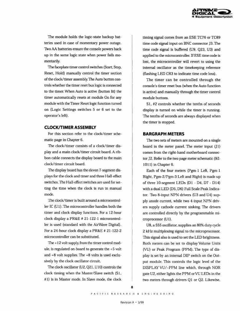
The module holds the logic-state backup bat
teries used in case of momentary power outage.
Two AA batteries ensure the console powers back
up in the same logic state when power fails mo
mentarily.
The faceplate timer control switches (Start, Stop,
Reset, Hold) manually control the timer section
of the clock/timer assembly. The Auto button con
trols whether the timer reset bus logic is connected
to the timer. When Auto is active (button lit) the
timer automatically resets at module On for any
module with the Timer Reset logic function turned
on (Logic Settings switches 5 or 6 set to the
operator's left).
CLOCKITIMER ASSEMBLY For this section refer to the clock/timer sche
matic page in Chapter 6.
The clock/timer consists of a clock/timer dis
play and a main clock/timer circuit board. A rib
bon cable connects the display board to the main
clock/timer circuit board.
The display board has the eleven 7-segment dis
plays for the clock and timer and three Hall-effect
switches. The Hall-effect switches are used for set
ting the time when the clock is run in manual
mode.
The clock/timer is built around a microcontrol
ler I C (U 1) . The microcontroller handles both the
timer and clock display functions. For a 12-hour
clock display a PR&E # 21-122-1 microcontrol
ler is used (standard with the AirWave Digital).
For a 24-hour clock display a PR&E # 21-122-2
micro controller can be substituted.
The + 12 volt supply, from the timer control mod
ule, is regulated on-board to generate the +5 volt
and +8 volt supplies. The +8 volts is used exclu
sively by the clock oscillator circuit.
The clock oscillator (U2, Q21, U lO) controls the
clock timing when the Master/Slave switch (S 1,
#1) is in Master mode. In Slave mode, the clock
8
4 Equipment: Deecrlpt:lan
timing signal comes from an ESE TC76 or TC89
time code signal input on BNC connector 13. The
time code signal is buffered (U9, Q23, U3) and
applied to the micro controller. If ESE time code is
lost, the microcontroller will revert to using the
internal oscillator as the timekeeping reference
(flashing LED CR3 to indicate time code loss).
The timer can be controlled through the
console's timer reset bus (when the Auto function
is active) and manually through the timer control
module buttons.
S 1, #2 controls whether the tenths of seconds
display is turned on while the timer is running.
The tenths of seconds are always displayed when
the timer is stopped.
BARGRAPH METERS The two sets of meters are mounted on a single
board in the meter panel. The meter input (J 1)
comes from the right-hand motherboard connec
tor 12. Refer to the two page meter schematic (92-
1011) in Chapter 6.
Each of the four meters (Pgm-1 Left, Pgm-1
Right, Pgm-2/Pgm-3 Left and Right) is made up
of three lO-segment LEDs (D1 - D4, D7 - D14)
with a dual LED (D5, D6) Full Scale Peak Indica
tor. Two 8-input NPN drivers (U3 and U4) sup
ply anode current, while two 4-input NPN driv
ers supply cathode current sinking. The drivers
are controlled directly by the programmable mi
croprocessor (U 1) .
U8, a 555 oscillator, supplies an 80% duty cycle
2 kHz multiplexing Signal to the microprocessor.
This Signal also is used to set the LED brightness.
Both meters can be set to display Volume Units
(VU) or Peak Program (PPM). The type of dis
play is set by an internal DIP switch on the Out
put module. This controls the logic level of the
DISPLAY VU/ -PPM line which, through NOR
gate U2, either lights the PPM orVU LEDs in the
two meters through drivers Q1 or Q2. Likewise,
PAC I FIe RES EAR C H & E N GI NEE R I N G
Revision A • 3/99

the -PGM2/PGM3 line controls NOR gate U7 to
tum on either the PGM2 LED or the PGM3 LED
through drivers Q3 or Q4. This is in response to
the setting of the Output module's PGM-2/PGM-
3 meter switch.
The meter supply voltages (+5V LOGIC and
LED POWER) are protected through polyfuses
F1 and F2.
AIRWAVE UNIVERSAL POWER SUPPLY For this section refer to the two power supply
schematic pages in Chapter 6. For a more com
plete discussion of the Power Supply refer to the
AirWave Universal Power Supply Technical Manual
(PR&E # 75-41).
The AirWave Universal Power Supply (AUPS)
consists of a power transformer, selectable for 115
VAC or 230VAC operation, chassis-mounted rec
tifiers and filter capacitors and a regulator circuit
board mounted to a heat sink.
The power supply is protected by a replaceable
AC mains fuse located in the power entry module,
thermal circuit breakers (auto-reset type) within
the transformer primary, internal fuses on the
transformer's critical secondary outputs and self
protected current-limiting regulators.
The power transformer has four secondary wind
ings. Three are wired to bridge rectifiers and filter
caps mounted on the chassis floor, while the fourth
is connected to a bridge rectifier (CR6) and filter
cap on the regulator circuit card. All voltage regu
lators fasten to the heat sinks.
The power supply has five output voltages:
• +5 volts @ 6.5 A for the console's logic circuitry
• + 12 volts @ 4.0 A for the clock/timer
• ±16 volts @ 1.0 A each for the audio circuitry
• +45 volts phantom @ 0.100 A for condenser
microphones.
The +5 volt (U2) and +12 volt (Ul) regulator
circuitry is identical with only their divider resis
tor values being different. The ± 16 volt regulator
9
Ai=nYAV~ DiGiL'AL ~ 4 Equipment: Ceecript:lan
circuitry (U3 and U4) employs a dual voltage
tracking device (U 5) that monitors the regulated
voltage outputs. If either voltage drops, the other
will follow to keep the two voltages equal.
The +45 volt supply uses a pass-transistor de
sign (Q1, Q2, CR5). Zener diode CR5 clamps the
base voltage of Q1 and the collector of Q2 to a
maximum of +47 volts. Q 1 and Q2 automatically
adjust the current to keep the supply voltage con
stant. The nominal output voltage will typically
be +45 volts.
PACIFIC RESEARC H & ENGINE ERING
Revision A • 3/99
rvI~~i@~!lte & ····)\]igiIFrtent
4i=n~=-=---i>iGiL4~ >
Fr troubleshootin,," the optional AJrW .. ,
Digital module extender (PR&E # 99-1014) allows
easy access to any module's circuit board test points.
Note that two module extenders are required for
troubleshooting the Monitor module.
Parts and Repair Services All of the switches. button caps and faders are
easily field replaceable. Although schematics are
included for field troubleshooting purposes. it is
recommended that modules be returned to PR&E
for circuit board service due to their surface mount
construction.
PARTS ORDERING & REPAIR INFORMATION
Spare parts. accessories and additional modules
can be purchased through a sales representative
or through PR&E's Customer Service Department.
To expedite the ordering process. and ensure the
correct parts are ordered. have the PR&E part
numbers at hand when ordering.
Most repair parts are shipped the same day.
Modules and other assemblies may have lead times
exceeding two weeks. so order accordingly.
Parts returned to PR&E for service. exchange.
or credit must have an RMA (Return Material
Authorization) tracking number asSigned to them
by the Customer Service Department. Parts or
components returned without an RMA number
written on the outside of the packaging may be
subject to customer return or to an additional han
dling fee.
To order parts or request an RMA. contact
PR&E by phone. fax. e-mail or post:
Pacific Research & Engineering Attention: Customer Service Department 2070 Las Palmas Drive Carlsbad, CA 92009 USA
Phone: 760.438.3911,8:00 to 5:00 Pacific Time Fax: 760.438.9277 E-mail: [email protected]
All parts orders and serviced parts are shipped
FOB Carlsbad using UPS Groundtrak in the USA.
unless otherwise speCified by the client. Federal
Express or UPS two-day. overnight and Next Day
A.M. delivery is also available for most items.
Orders must be placed before 2:00 PM PacificTnne.
and shipping method must be specified at time of
order. for parts to go out the same day.
Parts orders or repair services can be charged
to American Express, VISA or Mastercard, or
shipped COD, if not on-account with PR&E. Con
tact a sales representative for account information.
SPARE & REPLACEMENT PARTS INFORMATION
All PR&E parts are categorized using a two digit
part type prefix. a dash. and a three or four digit
part ID number (a second dash and a suffix num
ber may also be used to identify part variations).
The Replacement Parts table on the next page lists
the AirWave Digital parts typically subject to wear
and tear. It is recommended that one or more of
each of these be kept in the on-site spares stock.
PACIFIC RESEARCH & ENGINEERING
Revision A • 3/99
AirWave Digital Replacement Parts
PR&E # Description or Use 11-53 Bridge Rectifier # 12-95 On, Off, Talkback lamp & housing 12-101 On, Off, Talkback lamp only # 20-106 Voltage Regulator, adjustable # 20-107 Voltage Regulator, adjustable # 24-98 Cue Pot 24-100 CR and Studio Monitor, Headphone Pot 25-853 Pgm and AlB select switch * 25-854 Autofeed switch * 25-855 Cue switch * 25-856 Off/Line switch * 25-858 Module On switch ** 25-859 Module Off switch ** 25-860 Talkback switch ** 25-870 White button cap *** 25-871 Red button cap *** 25-872 Yellow button cap *** 90-1016 Input & Telco module fader
# Supplied in 76-728 Spare Parts Kit. * Used on the 95-968-x switchboards.
** Used on the 95-969-1 and -2 switch boards.
*** Blank button cap numbers. Also used for custom button engraving. Add a-I suffix for standard engraVing (Talkback. On. Off).
The AirWave Digital Assemblies & Modules
table lists the modules and assemblies available
for field servicing of the AirWave Digital console.
INSTALLATION KIT PARTS The installation kits (Tool kit, Connector kit for
the mainframe and for each Input, Telco, Mic Pre
or RLS and a Spare Parts Kit) are shipped with
each new console. The kit contents and quantities
are listed in the table below.
Connector and Tool Kit Components PR&E # Description or Use Qty.
76-752 Mainframe Connector Kit 14-482 3-pin AMP housing 9 14-484 6-pin AMP housing 21 14-486 8-pin AMP hOUSing 1 15-938-1 Receptacle contacts 162 50-5 AA Lithium battery 2
76-752-1 Input Connector Kit 14-484 6-pin AMP housing 2 14-513 24-pin AMP housing 1 15-938-1 Receptacle contacts 22
76-752-2 Telco Connector Kit 14-484 6-pin AMP housing 3 14-482 3-pin AMP housing 1 15-938-1 Receptacle contacts 23
76-752-3 Analog RLS Connector Kit 14-484 6-pin AMP housing 9 15-938-1 Receptacle contacts 54
76-752-4 Digital RLS Connector Kit 14-484 6-pin AMP housing 9 15-938-1 Receptacle contacts 27
76-727 AirWave Tool Kit 70-44 Sifam knob removal tool 1 70-90 Hex Wrench 1 70-126 Crimp Tool 1 70-129 Contact Removal Tool 1 90-151 Clock Magnet Tool 1
AirWave Digital Assemblies & Modules PR&E# 23-1 23-2 80-1551 95-895-1 95-895-2 95-968-2 95-968-4 95-968-6 95-968-7 95-968-8 95-969-1 95-969-2 95-974 95-1007 95-1008 95-1009 95-1011
Description or Use PR&E # Description or Use Electret microphone 99-960 Timer Control module Cue speaker 99-961 Microphone preamp module Blank Panel (one module space) 99-965-1 Monitor module Clockltimer Assembly (12 hour) 99-966 Analog Remote Line Selector module Clockltimer Assembly (24 hour) 99-1001 Analog Input SIM Timer Control switchboard 99-1002 Digital Input SIM Mon 2 & R1S switchboard 99-1003 B Logic Interface SIM Output Assignment switchboard 99-1004 Line Input module Line Input switchboard 99-1005 Telco Input/Output module Telco switchboard 99-1006 Output Amplifier module OniOffswitchboard 99-1010-1 Left DSP Card Talkback switchboard 99-1010-2 Middle DSP Card (AWD-20 only) Motherboard Interconnect 99-1010-3 Right DSP Card Left-end Motherboard 99-1012 Digital Remote Line Selector module Mid-Motherboard (AirWave Digital-20 only) 99-1014 Extender Card Right-end Motherboard (with power cable) 99-1015 Power Supply Assembly Bargraph Meter assy
2
PACIFIC RESEARC H & ENGINE ERING
Revision A • 3/99
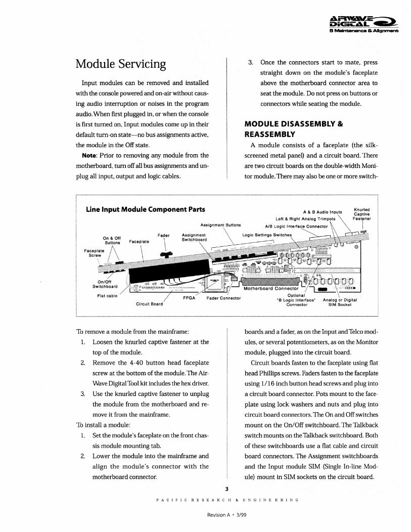
Module Servicing Input modules can be removed and installed
with the console powered and on-air without caus
ing audio interruption or noises in the program
audio. When first plugged in, or when the console
is first turned on, Input modules come up in their
default turn-on state-no bus assignments active,
the module in the Off state.
Note: Prior to removing any module from the
motherboard, turn off all bus assignments and un
plug all input, output and logic cables.
Line Input Module Component Parts
ASSignment Buttons
On & Off
Faceplate Screw
OnlOff Switchboard
Flat cable
Circuit Board
To remove a module from the mainframe:
1. Loosen the knurled captive fastener at the
top of the module.
2. Remove the 4-40 button head faceplate
screw at the bottom of the module. The Air
Wave Digital Tool kit includes the hex driver.
3. Use the knurled captive fastener to unplug
the module from the motherboard and re
move it from the mainframe.
To install a module:
1. Set the module's faceplate on the front chas
sis module mounting tab.
2. Lower the module into the mainframe and
align the module's connector with the
motherboard connector.
3
5 Mai..-....ce & Alignment
3. Once the connectors start to mate, press
straight down on the module's faceplate
above the motherboard connector area to
seat the module. Do not press on buttons or
connectors while seating the module.
MODULE DISASSEMBLY & REASSEMBLY
A module consists of a faceplate (the silk
screened metal panel) and a circuit board. There
are two circuit boards on the double-width Moni
tor module. There may also be one or more switch-
. Knurled A & B AudiO Inputs Captive
Lelt & Right Analog Tri \ Fastener
AlB Logic I nterlace Connector I Logic Settings
Optional "8 Logic Interface ll
Connector
boards and a fader, as on the Input and Telco mod
ules, or several potentiometers, as on the Monitor
module, plugged into the circuit board.
Circuit boards fasten to the faceplate using flat
head Phillips screws. Faders fasten to the faceplate
using 1/16 inch button head screws and plug into
a circuit board connector. Pots mount to the face
plate using lock washers and nuts and plug into
circuit board connectors. The On and Off switches
mount on the OnlOff switchboard. The Talkback
switch mounts on the Talkback switchboard. Both
of these switchboards use a flat cable and circuit
board connectors. The ASSignment switchboards
and the Input module SIM (Single In-line Mod
ule) mount in SIM sockets on the circuit board.
PACIFIC RESEARC H & ENGINE ERING
Revision A • 3/99
Circuit Board Removal
To remove the circuit board from the faceplate:
1. Unplug all faders, pots and switchboards,
as applicable.
2. Remove the Assignment switchboard sup
port screws.
3. Remove the circuit board mounting screws.
4. Separate the circuit board from the faceplate.
Reassemble in reverse fashion, ensuring that
the switchboard buttons and connectors protrude
through the faceplate without binding.
SIM Circuit Card Removal
1. If necessary, remove the circuit board from
the faceplate per the previous instructions.
2. Using antistatic material, set the circuit
board trace side down.
3. Press out on the two metal switchboard lock
ing clips while lightly pressing on the bot
tom of the circuit card. The board tilts out
of the locking clips toward the switch or
component side.
4. Lift and remove the SIM card from the SIM
socket.
SIM Circuit Card Installation
1. Using antistatic material, set the circuit
board trace side down.
2. Insert the SIM card with the edge contacts
inserted into the SIM socket at about a 45°
angle, with the switches! components angled
down. The board is keyed so it will only
mount in the correct orientation.
3. Press the circuit card into the socket while
moving it to a vertical position. The locking
clips will snap and hold the board in place.
When correctly positioned, the circuit card will
be vertical to the circuit board and the two SIM
socket alignment tabs will be set into matching
holes on the SIM card.
4
.4i=1wav.;- = DiGL.4~ .> 1!I~1_ .... _&AIIa~
On/Off or Talkback Switchboard Removal
1. Remove the circuit board from the faceplate,
per previous instructions.
2. Remove the # 1 Phillips screws, lock wash
ers and washers from the switchboard to re
move it from the faceplate. There are two
screws on the Talkback switchboard and
four screws on the On/Off switchboard.
3. Unplug the flat wire cable from the switch
board connector. Note its orientation.
Optional "B" Logic Interface Installation
1. Using antistatic material, set the module
with its circuit board trace side down.
2. Position the "B" Logic card's 24-pin logic
connector into the faceplate opening at an
angle in order to insert the card's PI con
nector into the circuit board connector pins.
When properly mounted, the two 24-pin
logic connectors will be physically aligned.
MONITOR MODULE The Monitor module has two circuit boards on
one faceplate. Prior to removing the Monitor mod
ule, unplug the headphones from the module and
turn off the external amplifiers for the Control
Room and Studio monitors and headphones. This
prevents possible transient noise damage to the
loudspeakers and headphones.
The Monitor 1 circuit board must be removed
in order to remove the Monitor 2 circuit board.
All of the faceplate components-pots, headphone
jack, Talkback mic, and the Monitor 2 circuit
board, plug into the Monitor 1 board.
AirWave uses sealed pots that do not require
"cleaning." If it becomes necessary to replace a
pot, remove the Monitor 1 circuit board from the
faceplate by unplugging all cabling and removing
the three mounting screws. Remove the colored
end cap from the knob by prying it loose. Use the
70-44 Sifam Knob Removal Tool to loosen the lock
PACIFIC RESEARC H & ENGINE ERING
Revision A • 3/99
nut so the knob can removed from the pot shaft.
Use a 7/16 inch nutdriver to remove the shaft nuts.
FADER SERVICING There are no replaceable nor rebuildable parts
on the AirWave Digital fader assembly. Fader ser
vice is comprised of cleaning and lubricating. All
faders are conductive plastic, single-element fad
ers (PR&E # 90-10 16) .
If the fader movement is rough, either the lubri
cant on the glide rails has evaporated or foreign
material has gotten into the fader. Dow Corning
510 is the preferred glide rail lubricant as it will
not migrate to the contact fingers like other lubri
cating oils.
Fader Disassembly and Cleaning
1. Remove the module from the mainframe.
2. Remove the circuit board from the faceplate,
per previous instructions.
3. Remove the fader knob and the two fader
mounting screws, and then the fader from
the faceplate.
4. Remove the snap-on fader assembly cover.
It is held in place by round stamped bosses
at each end. With the fader sitting label up
and the connector pins to the front, a pry
point is on the right end of the fader cover.
5. Clean the fader using only a dry cotton swab,
or a cotton swab wet with distilled water.
Note: The use of chemical cleaners on the con
ductive plastic will substantially shorten fader life.
Never touch the fader slider contact fingers while
cleaning the fader parts.
Use only a dry cotton swab, or a cotton swab
wet with distilled water, to clean the fader parts.
Always use a clean dry swab to dry off the con
ductive plastic tracks after cleaning. If the fader
rails are noticeably dirty, wipe them off using a
dry cotton swab before lightly lubricating the top
rail with Dow Corning 510.
5
If coffee, a soft drink or other sugared liquid
has been spilled into the fader, remove it from the
module as soon as possible and remove the top
cover of the fader. Hold the fader under hot run
ning water while moving the fader slider back and
forth to dissolve the sugars and other chemicals.
Thoroughly dry the rails and conductive plastic
using dry cotton swabs and then lubricate the top
fader rail with Dow Corning 510.
Lubricating the Glide Rail
Move the fader slider to the middle of its travel
and place one drop of Dow Corning 510 lubricant
on the top rail on either side of the fader slider
bushings. Move the slider through its full travel to
distribute the lubricant. Wipe off any excess lu
bricant from the rubber stops at each end of the
glide rail. Normally only the top rail (the one the
fader slider bushings glide on) requires lubricant.
MICROPHONE PREAMP MODULE The microphone trim pots are under a faceplate
security cover. They are set at the factory for a +4
dBu output level with a-55 dBu, 1 kHz input. In
the field, each trimpot can be adjusted for the spe
cific microphone being used on that preamplifier.
ANALOG LINE INPUT MODULE The Trim L andTrim R trimpots (R60 and R59)
set the left and right channel gain, respectively.
To adjust these trimpots:
1. Set the fader at the -12 dB (nominal) mark
and assign the module to Program 1.
2. Apply a 1 kHz Signal at the nominal input
level for that channel (from -10 dBu up to
+4 dBu) to the left and right input connec
tors. Either the A or B input can be used, as
the adjustment point is after the AlB switch.
3. Using the Program 1 bargraph meters, ad
just the trimpots for OVU (or -8 PPM).
PACIFIC RESEARCH & ENGINEERING
Revision A • 3/99
TELCO INPUT/OUTPUT MODULE There is one trimpot adjustment on the Telco
module. The trimpot (RV1) is used to set the in
put level from the hybrid (-10 to +4 dBu) so that
a nominal +4 dBu output is available at the leftTo
Tape output connector. To set RV 1:
1. Connect a 1 kHz signal to the From Hybrid
connector using the hybrid's output level.
2. Monitor the To Tape Left output.
3. Adjust RVI for a +4 dBu output.
OUTPUT MODULE To access the Output module analog level
trimpots, the module must be placed on an ex
tender card (PR&E # 99-1014). There are seven
trim pots to adjust the analog signal output levels.
There are no adjustments for the digital outputs
or for the bargraph meters.
Before adjusting the program output levels, the
meter selector DIP switch (DS 1, switch 2) must
be set to VU and one Input module must first be
set up as a "standard" so that a known input level
is feeding the Output module amplifiers. To set up
an Input module as a standard:
1. Connect an analog +4 dBu, 1 kHz balanced
signal to the left and right inputs on the A
Input.
2. Set the fader to the nominal -12 dB mark.
Select A Input and assign the module to all
three program buses.
3. Adjust Trim L and Trim R for OVU dBu in
dications on the Program 1 left and right
meters.
Do not change the standard module settings
until after the Output module adjustments are
completed. To set the Output module:
1. Place the Output module on an extender
card.
2. Turn off all other Input and Telco modules,
leaving only the "standard"Input module On,
6
Ai=nYAV~ iOiGii:'AL ~ E5 Maintenance & Alignment:
feeding all three program buses with the
1 kHz input at nominal level.
3. Plug an ACVoltmeter into the analog Pgm-
1 left output. Adjust RV3 for +4 dBu. Move
the AC Voltmeter to the analog Pgm-1 right
output. Adjust RV2 for +4 dBu.
4. Move the ACVoltmeter to the analog Pgm-2
left output. Adjust RV 4 for +4 dBu. Move
the ACVoltmeter to the analog Pgm-2 right
output. Adjust RV5 for +4 dBu.
5. Move the ACVoltmeter to the analog Pgm-3
left output. Adjust RV6 for +4 dBu. Move
the ACVoltmeter to the analog Pgm-3 right
output. Adjust RV7 for +4 dBu.
6. Select Pgm-1 for the Monaural Output.
Move the AC Voltmeter to pins 1, 2 and 3 of
the Mono output connector. Adjust RV 1 for
+4dBu.
MONITOR MODULE The only trimpot (RVl) on the Monitor 1 cir
cuit board sets the built-in Talkback microphone's
output level. It is acljusted through the front panel.
There are no adjustments on the Monitor 2 board.
CLOCK/TIMER ASSEMBLY There is one frequency adjustment (C2) on the
board. Allow at least one hour of powered opera
tion to stabilize the internal oscillator before ad
justing the frequency. To adjust the master clock
oscillator, monitor the CLK test point using a xl 0
probe with a high-frequency counter. Adjust C2
for exactly 3.276800 MHz.
Clock/Timer Troubleshooting
Red LED Dashing below dock: Clock set for Slave mode
without ESE time code on J3. Change switch
S 1, # 1 from Off to On if ESE is not being
used. Test ESE system if time code is feed
ing J3.
PACIFIC RESEARC H & ENGINE ERING
Revision A • 3/99
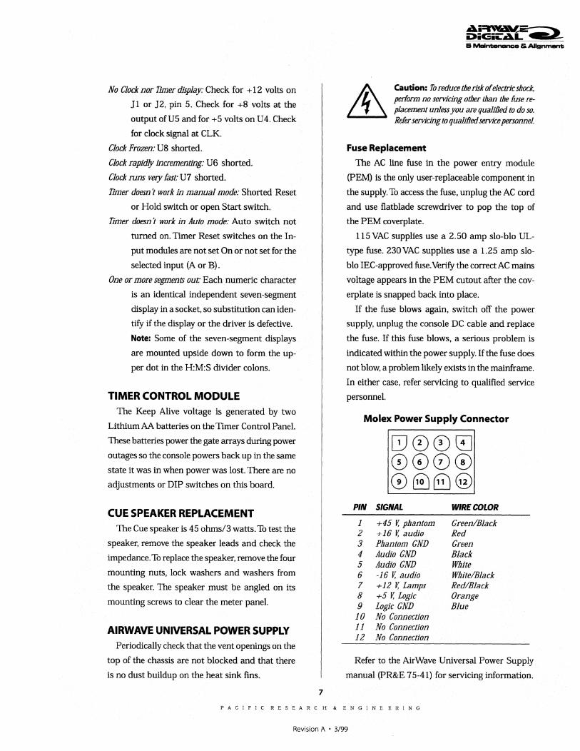
No Clock nor Timer display: Check for + 12 volts on
11 or 12, pin 5. Check for +8 volts at the
output ofU5 and for +5 volts on U4. Check
for clock signal at CLK.
Clock Frozen: U8 shorted.
Clock rapidly incrementing: U6 shorted.
Clock runs very fast: U7 shorted.
Timer doesn't work in manual mode: Shorted Reset
or Hold switch or open Start switch.
Timer doesn't work in Auto mode: Auto switch not
turned on. Timer Reset switches on the In
put modules are not set On or not set for the
selected input (A or B).
One or more segments out" Each numeric character
is an identical independent seven-segment
display in a socket, so substitution can iden
tify if the display or the driver is defective.
Note: Some of the seven-segment displays
are mounted upside down to form the up
per dot in the H:M:S divider colons.
TIMER CONTROL MODULE The Keep Alive voltage is generated by two
Lithium AA batteries on the Timer Control Panel.
These batteries power the gate arrays during power
outages so the console powers back up in the same
state it was in when power was lost. There are no
adjustments or DIP switches on this board.
CUE SPEAKER REPLACEMENT The Cue speaker is 45 ohms/3 watts. To test the
speaker, remove the speaker leads and check the
impedance. To replace the speaker, remove the four
mounting nuts, lock washers and washers from
the speaker. The speaker must be angled on its
mounting screws to clear the meter panel.
AIRWAVE UNIVERSAL POWER SUPPLY Periodically check that the vent openings on the
top of the chassis are not blocked and that there
is no dust buildup on the heat sink fins.
7
Caution: To reduce the risk of electric shock, perform no servicing other than the fuse replacement unless you are qualified to do so. Refer servicing to qualified service personnel.
Fuse Replacement
The AC line fuse in the power entry module
(PEM) is the only user-replaceable component in
the supply. To access the fuse, unplug the AC cord
and use flatblade screwdriver to pop the top of
the PEM coverplate.
115 VAC supplies use a 2.50 amp slo-blo UL
type fuse. 230VAC supplies use a 1.25 amp slo
blo IEC-approved fuse. Verify the correct AC mains
voltage appears in the PEM cutout after the cov
erplate is snapped back into place.
If the fuse blows again, switch off the power
supply, unplug the console DC cable and replace
the fuse. If this fuse blows, a serious problem is
indicated within the power supply. If the fuse does
not blow, a problem likely exists in the mainframe.
In either case, refer servicing to qualified service
personnel.
Molex Power Supply Connector
PIN SIGNAL WIRE COLOR
1 +45 V, phantom Green/Black 2 +16 V, audio Red 3 Phantom GND Green 4 Audio GND Black 5 Audio GND White 6 -16 V, audio White/Black 1 +12 V, Lamps Red/Black 8 +5 V, Logic Orange 9 Logic GND Blue 10 No Connection 11 No Connection 12 No Connection
Refer to the AirWave Universal Power Supply
manual (PR&E 75-41) for servicing information.
PACIFIC RESEARC H & ENGINE ERING
Revision A • 3/99
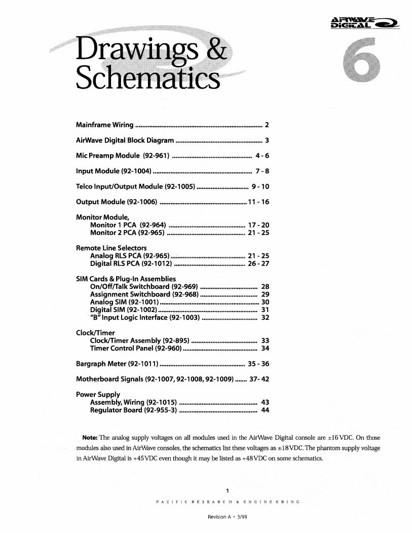
Mainframe Wiring ......................................................................... 2
AirWave Digital Block Diagram .................................................. 3
Mic Preamp Module (92-961) .............................................. 4 - 6
Input Module (92-1 004) ......................................................... 7 - 8
Telco Input/Output Module (92-1005) .............................. 9 - 10
Output Module (92-1 006) .................................................. 11 - 16
Monitor Module, Monitor 1 PCA (92-964) ............................................ 17 - 20 Monitor 2 PCA (92-965) ............................................. 21 - 25
Remote Line Selectors Analog RLS PCA (92-965) ... ~ ....................................... 21 - 25 Digital RLS PCA (92-1012) ......................................... 26 - 27
SIM Cards & Plug-In Assemblies On/OfflTalk Switchboard (92-969) ................................. 28 Assignment Switchboard (92-968) ................................. 29 Analog SIM (92-1001) ......................................................... 30 Digital SIM (92-1 002) ......................................................... 31 liB" Input Logic Interface (92-1003) ................................ 32
ClocklTimer ClocklTimer Assembly (92-895) ...................................... 33 Timer Control Panel (92-960) ........................................... 34
Bargraph Meter (92-1011) ................................................. 35 - 36
Motherboard Signals (92-1007,92-1008,92-1009) ....... 37- 42
Power Supply Assembly, Wiring (92-1015) ............................................. 43 Regulator Board (92-955-3) ............................................. 44
Note: The analog supply voltages on all modules used in the AirWave Digital console are ±16 VDC. On those
modules also used in AirWave consoles, the schematics list these voltages as ± 18 VDC. The phantom supply voltage
in AirWave Digital is +45 VDC even though it may be listed as +48 VDC on some schematics.
PACIFIC RESEARC H & ENGINE ERING
Revision A • 3/99
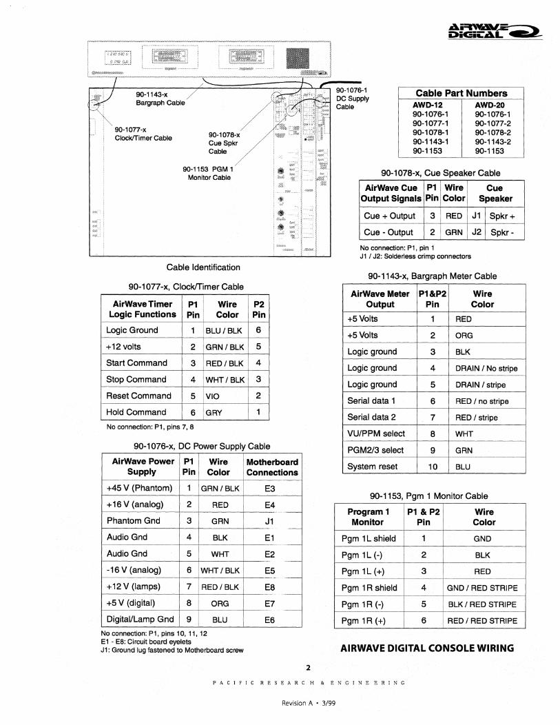
90-1143-x 8argraph Cable
90-1077-x Clock/Timer Cable 90-1078-x
Cue Spkr Cable
90-1153 PGM1 Monitor Cable
Cable Identification
90-1077-x, ClockfTimer Cable
AirWave Timer P1 Wire Logic Functions Pin Color
Logic Ground 1 BlU! BlK
+12 volts 2 GRN! BlK
Start Command 3 RED! BlK
Stop Command 4 WHT! BlK
Reset Command 5 VIO
Hold Command 6 GRY
No connection: P1, pins 7, 8
P2 Pin
6
5
4
3
2
1
90-1076-x, DC Power Supply Cable
AirWave Power 1 P1 Wire Supply IPin Color
+45 V (Phantom) 1 GRN! BlK I
+ 16 V (analog) 2 RED
Phantom Gnd 3 GRN
Audio Gnd 4 BlK
Audio Gnd 5 WHT
-16 V (analog) 6 jWHT! BlK
+12V (lamps) 7 RED! BlK
+5 V (digital) B
Digital/Lamp Gnd 9
No connection: P1, pins 10, 11, 12 E1 - E8: Circuit board eyelets
ORG
BlU
J1: Ground lug fastened to Motherboard screw
Motherboard Connections
~--
E3 ---
E4 - ~ ---
J1 -~- --
E1 ~ -----
E2 -~~-
E5 -~- ~-
EB --~~--
E7 - ~~ --
E6
2
90-1076-1 DC Supply Cable
Cable Part Numbers AWO-12 AWO-20 90-1076-1 90-1076-1 90-1077-1 90-1077-2 90-1078-1 90-1078-2 90-1143-1 90-1143-2 90-1153 90-1153
90-107B-x, Cue Speaker Cable
AirWave Cue P1 Wire Cue Output Signals Pin Color Speaker
Cue + Output 3 RED J1 Spkr+
Cue - Output 2 GRN J2 Spkr -
No connection: P1, pin 1 J1 I J2: Solderless crimp connectors
90-1143-x, Bargraph Meter Cable
AirWave Meter P1&P2 Wire Output Pin Color
+5 Volts 1 RED
+5 Volts 2 ORG
Logic ground 3 BlK
Logic ground 4 DRAIN! No stripe
Logic ground 5 DRAIN! stripe
Serial data 1 6 RED! no stripe
Serial data 2 7 RED! stripe
VU/PPM select B WHT
PGM2/3 select 9 GRN
System reset 10 BLU
90-1153, Pgm 1 Monitor Cable
Program 1 I P1 & P2 Wire Monitor i Pin Color
Pgm 1 L shield I 1 GND
Pgm 1 L (-) ,
2 BlK
Pgm 1L (+) 3 RED
Pgm 1 R shield 4 GND! RED STRIPE
Pgm 1R (-) 5 i BlK! RED STRIPE
Pgm 1R (+) I 6 I RED! RED STRIPE
AIRWAVE DIGITAL CONSOLE WIRING
PACIFIC RESEARCH & ENGINEERING
Revision A • 3/99
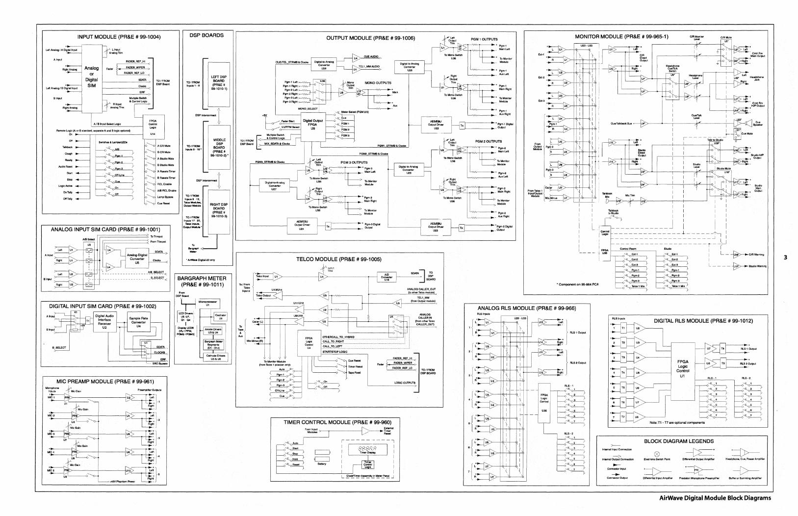
A Input
AiglrtAn ....
+ UtI: Analog I B Digl1allnp.lt
Blnput
INPUT MODULE (PR&E # 99-1004)
Analog or
Digital 81M
F ....
FADEFLREF ~
SCATA >
C"""" TO/FROM
DSP ... '"
r-____________ -=E~~> Multipi.SWitdl IlControlLogiQ
Rlnput :> Analog Trim
FPGA .,..,"'" Loge
Ramen. Logic (A or ~ standard, separate A and B logic optional)
~ .-----r-~----------------~
Oft Switch .. a. LampalLEDe
ToJ_
~:_1 t ecu,", - ~ --Sian ~="' t S ....
Log;c .....
U14
8CRMute
AStudloMqr.
BStudlotAlte
~RMmTlrner
B Reeeta Timer
RCLEnabie
DSPBOARDS
TO/FROM !npuIll1-8
LEFTDSP BOARD (PR&E#
99-101G-1)
f!.
OsP""""""""'1 V
TO/FROM ~,.".
MIDDLE DSP
BOARD (PR&E#
99-101G-2) •
On Tally
~::. t NBRCLEnabi.
Oft .... '" ~ ...... -Cu. R8MI
ANALOG INPUT SIM CARD (PR&E # 99-1001)
A Input >-__ ,"-
U2
B Input '>-__ ,"-
AnaIog-Digitai Converter
U5
SDATA"
-I AlB SELECT ~------------------~----<
-------------------~~~<
DIGITAL INPUT SIM CARD (PR&E # 99-1002)
__ L,,'~---I' f-l Dil=iO
TO/rAOM tnPU1l1 12,
TttooModuIM, Outpu1Modul.
TO/FROM InpuI6,7· 20, T.-oolnpulI,
OuIPUI Module *
To ........ '" -,
RIGHTDSP BOARD (PR&E#
99-1010-3)
BARGRAPH METER (PR&E#99-1011)
F .... asP .....
. tr~ [Le~~.;,~1
Receiver U2
Semple Rate Converter
U4
_ Q1 j04 i
l 'O;:7~:-1 POMI/PQM:I)
MIC PREAMP MODULE (PR&E # 99-961)
To/From T ....
Pgm-1l8ft
Pgm-1 Right Pgm-2Left
,,""'Aiglrt Pgm-3Left
Pvm-3 Right
r:; MuHipia Swillch
~-""",=eo","""='='=' =~
OUTPUT MODULE (PR&E # 99-1006)
CUE AUDIO >
TEL1_t.WAUDIO >-------;>
PGM1 STAMS. CI0ck8
PG~STRMB' CIockJ
~~~~~-----I~+Pgm-3
Mainlefl:
;> ToManitor'
" Module
~-~~'---+Pgm.3
~'1:.--"""+r--'" Main Right
0> ToMonitor :> Module
,1-------...... + Pgm-3Digital
LJ-----...... - Output
TELCO MODULE (PR&E # 99-1005)
INPUT
lR'" 1---"""'---' ~ :J BOARD I+T ... ".", U1
Hybrid + U1MJ14 ANALOG CALLER_OUT (tooth.IT_co module) >
T .... O~ r-------------~
~ V V ~ To Monitor Module
(frornTelco1 position only)
FPGA Logic
Com"" U4
I-----+~--~--~ us ,.--. ----j
~~:;-~~~-.---.-.... ---- .... -".-.-------.~ ~~:-!!I~_._-------.------------"----------------.--.-"-~ i "~":'!?=:.~~_"_""_"_""""_"""""""_""" __ """"""""_"" ________ " ______ J
ANALOG CALLER IN
(frornotherTelco CALLER_OUT)
Fade,
STARTISTOP LOGIC
:=-~~ ~ TO/FROM asPBOARO
LOGIC OUTPUTS L-_________________ >
TIMER CONTROL MODULE (PR&E # 99-960) I"----- ExIoma' F= :::>--.-------1L,/'/--+-r::
r-----------, I I I I I I I I I I
I
PGM 1 OUTPUTS MONITOR MODULE (PR&E # 99-965-1) ClRMonitor ...... CIA .....
f:;:;.-r-r--"""--r----1'" + Pgm-1 Main Left
... ToMonltof _ ModW.
4-"""""--_+ Pgin-1 _Left
1.lt--.rr--"""--r----1"'+ -Pgm-1
7'-tT"Nv-i-t-__ - Mam Rig'"
+ ToMonitor Modulo
Pgm-1 AuxAight
: + Pgm-1 Digital
J-------I_ ... - 0uIpu'
PGM 2 OUTPUTS
I~~r--"M'T--'" + ...... Main left
::> To Monitor Modulo
'-'A'V---+_+ Pgm-Z
AuxLoft
~~~~r-----+~m~
17-~h-"""+-r---l"- Main Right
'-'V\'V---+_+ ~-2
~"""--__l .. - AuxAigirt
: +P"".2DigilBl
J-------I_ ... _~~
I I I I
1-
• Component on 95-964 PCA
ANALOG RLS MODULE (PR&E # 99-966) RlSlnpute
'U 2{ ~
3{ ~
4U
·U ·U 7U
1"-.----1 ... + La.
t.efl)
:::~====:R:I~
FPGA L .... eo .. ""
U35
RLS10utput
RLS20uq,ut
RLSlnpu18
>-tntemallnput Connection
-> Internal OutputCoMdon -Connector Input
--""'""*"'u",",
CIA Di_ 0 ......
..... phono CualTalk
"""'"
I I l-
I - - - - -n;;;-sh;lo-r-___ +-_~ ____ ~U~
StuoioHIP + OulpUt
""die Main
+ Qutp"
DIGITAL RLS MODULE (PR&E # 99-1012)
FPGA Logic
Control Ul
RLS10utfM
---G:8:J1-__ RLS-l~ ... 2 ;....
BLOCK DIAGRAM LEGENDS
~=1>--- ~=&c- -{>-DI"~ InputAmpltft., PraclaionMiClqlhonePreamplifier BufferorSUmming Amplifier
AirWave Digital Module Block Diagrams
3
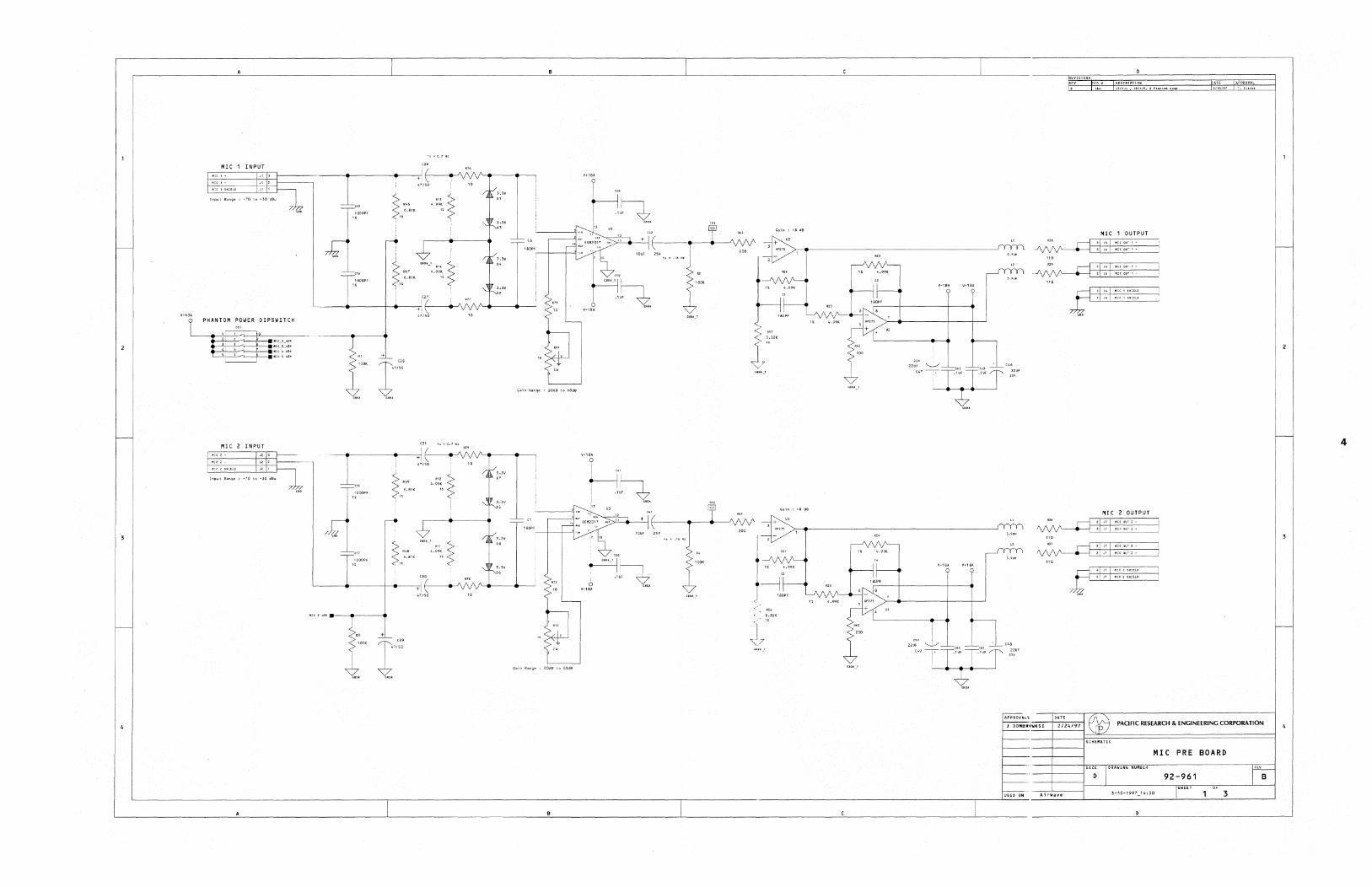
POWER DIPSWITCH
~:oo'"
"
". IOOOPF
"
1m ~
:oo'"
/. {,.{
on
1000PF
"
~ ." 6.811(
n
•
I
'" ~' 4.99(
" ,
""-'.n ~' 4.99K
n
GaIn hnse: aOdS to 60dB
Ga;nRange
V+,8A
Q
I '" H'i : .,rlz.
,,, 3.321(
'.~ R56
3.32K
25V ; en
22UF'-.....i.../,u;p~6JF .1UF C47 :'
i
ijMo.I.
HIC 1 OUTPUT
'~:::NlCOUT\' ,,, ,',,' ~21~ '"
HIe 2 OUTPUT
'I " 1 """": ~2.Jl.lIreou'2
I'''''"'''' f: I ::".,,",,,,
PACIFIC RESEARCH PORAllON &ENCINEERINGCOR
MIt PRE BOARD
92-961 SH ET OF
3-10-1997_'4:30 3
4
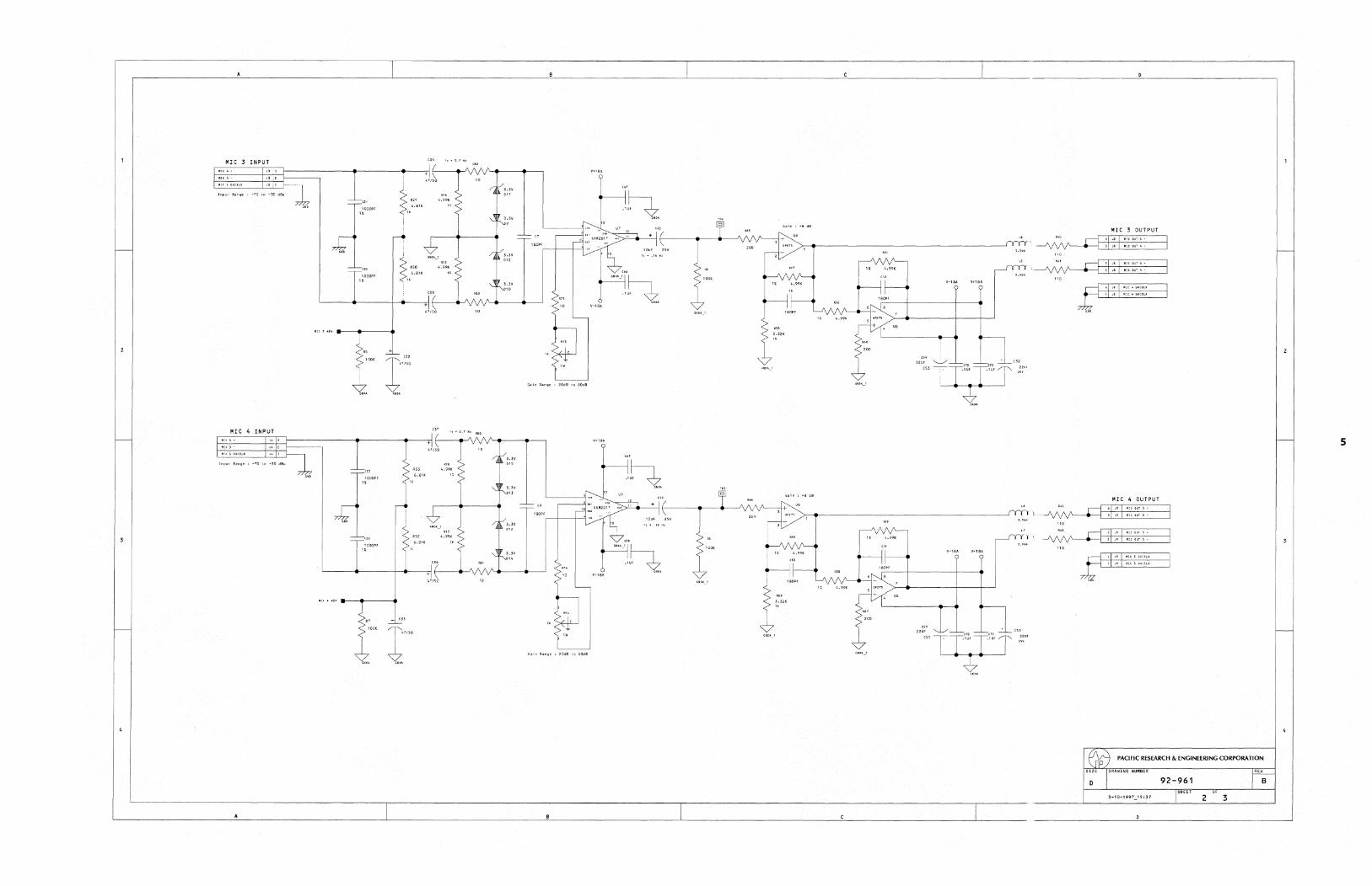
.. y~'"
1000PF
"
~i os,
6.8111:
"
~i 'so
6.81K
"
" 20dBto60d8 G .. inRange.
I"'C'SHIELO :,:: .;" .. ,,"
OS> 2 '~:Y 0~m ~l~F 2~!lIt 2" ___ .IUF • C53 :"
!
GIU
MIC 4 OUTPUT
,'''' m'":': .-~3.J9.lIlCOU'3 3.?"· !lleOUTl. ----
,SO 22Uf
"!COU,'-
---------:-:.-::~ RPORATION ENGINEERING CO PAOFIC RESEARCH & OE.
DRAWING NUMBER
D L __ _ 92-961
SHEET 2 OF_3:::..-__ _
B
5
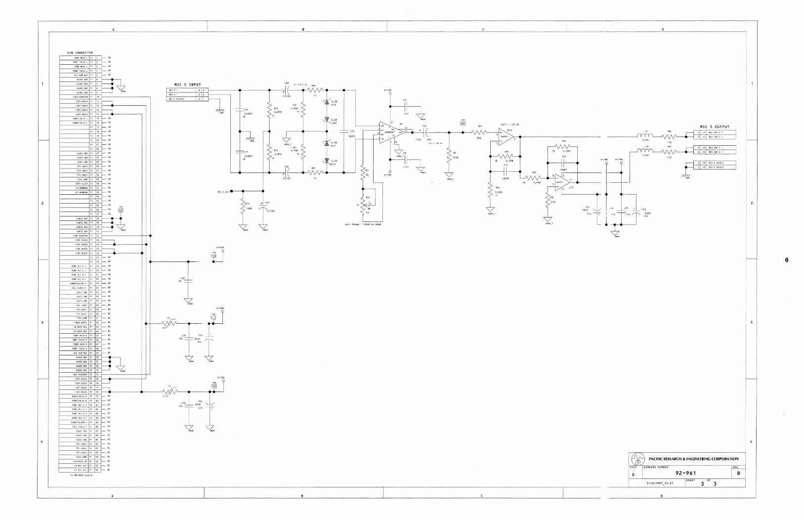
DIN CONNECTOR
PGMI M~tNL PI 1 ~ NC
PGfII1TELCOLPl 2 ~NC
PGMZ ,",UN L PI 3 :........- NC
~--~~~~~f-~-- " AUOIOGNDP16~-". AUOIOGND PI 7
I--------.=U,::,,'-',=,,+,,'-+'--l GNDA
AUDIOGND PI 9
I-----~=::~~~~:~:~t= :: PI 17 I-- NC
PI 18 I-- NC
~--------~~",-+,::::,~~ :: I-------------l~~~~ "
PI 22 ~NC
I--------=:::..c~~~:~:~t= :: 25 I-- NC
I--------=~~~~,::.~~ "
1--------2~~~f::::~~ ::
I-------~~~~f::::~~ :: 31 I-- NC
I-------~==~~f,::,~~ " PI 33 I-- NC
PI 34 I-- NC
PI 35 1-- NC
PI 36 1-- NC '-' ,:: ~"
+18VAUDIO PI :: J--l -'''"m'' :: J--l
1___----------l~~~1--- " PI 48~NC
PGMI OUT L - PI 49 I-- NC
PI 50 I-- Nt
I-----~~~~::,,'-+,::,~~ :: PI 53 1-- NC
1---" 1___---=~~--l~f,::,~1___ " 56 I-- NC
I___----:::::::..c~~~,::,~~ " 58 I-- Nt
~----~~~~~,::.~~ " 1---____ -2~:::..c~+="~~ NO
I-------~~=-~~:;~~ :: I-------==:::..c~~f·::'~-- " I-------~~~~~.::.~== :~
I-----~~~~~f·::·~== :: I-----~~~~~f'::·~-- "
69 _NC
AUDIOGND PI 70
1--------------+'-'--+'--1" B ~
1-----~~~~~~'~.~1--- " PGJI1.uHLCO~ PI 80 ~ NC
81 I-- Nt ~--~~~--j~~,::,~~ "
I-----~~~~~f'::'~~ :: SENDfCALLER + PI 1-- NC
1---__ ~:::..c::::::--j~~'::.~1--- " I___ NC 1-------:::::::..c=4~~,::,~1___ "'
1-------:::::::..c=4~~.::,~t= :: I-------~~~=-f·::'~~ " I___----~~:::..c~+::::~== :~
I-------~==~~+.::.~-- " I-------~~~~+.::'~-- " L-____ ~~:::..c~~~-- "'
to MOTH£Rboard
MIC INPUT
1000PF
"
Mle 5 40V .. --... ------...
+ C40
3.3V
'"
3.3V
""
3.3V
01'
V+18A
180PF~+ __ +--1
h ,
""-'h ~
~ !
U10
laOPF
MIC 5 OUTPUT
----------~~~:::~I::~::::~I~~~----~ '"
'"Tip
6
PACIFIC RESEARCH & ENGINEERING CORPORATION
REV
92-961 B SHEET OF
3 3
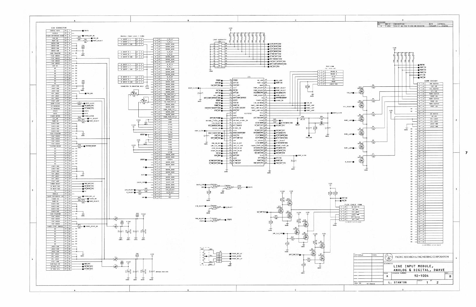
DIN CONNECTOR
+48VPIIANTOM P' 10 - NC G~ f--"':'::~'::=~-Ir.pc.-, r.:"2'C-l~ GNDA
.'6VAUIII0
-'6VAuno
P' "rNC P116rMC
PI l1 r NC
PI 18 r-- IIC
PI ,9 t-- NC
PI 20t--- NC
p, 21t---Ne ~
f---~~--~~22~r- "' lr
644'S
FADER IIIPER
P6M2.0N
AUDlO GMO
+1&V AUOIO
+16-VAUDl'O
~16V Auno
PI 30
PI 31
PI 32
PI 42.t--- Me
P1 ::0 Pl::h
~RKE::A:\\VLE <rmn1'l: 2.56F$
FADEltWIPER
604 R67 :: :~~2 S:~~::T
PI 47 __ l'V1llli"'lIm
48 r-- Ne 604
f----~~----r.P~'t74.~r_ " P1 50t--- Me
PI 51 t-- Ne
PI 52. t-- lit
PI 53t--- lit
PI 54t--- lit
P155R
" "
f---.";'"C7.,,::-,,;.;,-+;;-t-;'~9 &ND-" PI58R
+SV LOGlC 60
+12VLAMP PI 61
CRMUTEBUS
STMUTEBUS-
" P166 r
~~ .. ~'~. ~,,~,~,,~,,~,,~,,~,~p~'B~~?~~'~":ER REF LO , .. " " ".. ." "" ---"'~'-" paM5 ON P'M5_SELECT
AUDIQ&No Pl10R AUDIO &NO 11
AUDIO &NO 12
AUDIO 6ND 75
+48V PHANTOM P1 74 r-- IIC
::::::::: ::;:h :::: ::::: :::: r-----l
'" FADER START ENABLE PI 79
80t--- IIC 604
f----~~----~P~'~'~, r- NC
+SV LOGIC
.5V LO&IC
+5V LOGIC
CR: Mle GIL
ST MIC OIL
P1 82 t-- NC
P1 83.t-- Nt
P184rNC
P1 85 f-- IIC
PI 86~NC
" "9 .. .. " 90 r---,
" f----4 " 92
" 95
" 94
" 95
" 96
+ GIIOO
No.lnallnputLevel :+4dBu
V+SO ...bC .,,":+::-+--=;:----? iNDO
V+iD l
V+,20
A!B_SELECT ..
B_HLECT_ 604 62
-~+:+---;;;-;---; ERf_L---'----'-____ ~
~V+I6A
~I" """ '" '" GNDD
L06ICttPSilITCH DSI _ _
r-~--~'---¥~~-t-lr-t--r-t-lr-t--r-t ___ ~eRYUfEYSW
t~~~~~~~~~~~~~~~~~~~~~ ~ 11 ~
" " 12
"
=.--'-"q= '!'JOlf 3 H'fYIi ~ 13 WlJm'
rr~A~"~'~E~"~"; :==t~ A!a_SELECT RtLENABLE_DSW 39~
a-DUAL_EN .-r-,~':-I B-DUAL_EII
KIiEP ALIVE .r;;;;:;:;:;:;;~++=~l;~",,= - :l,liuXL [olifc_kEV bOAL LoUE kEY
~I-: OFF_:~:=::~·+-t-~,:q~_tLk L~vpp
&HiD PWR_ON_RST 47 PtlR_ON_RST
LMP_tLK_COM U"3LK_COM
STOP_PUt.SE STOP_PUI.SE
START_'ULSf: URT_PULSE
u:w lDV ~.--r-~~
~&ND5 ~.--t-'='q~ ;;::m:rrr:Dli 50 A=THA=df
A!8_$tLECT~8SE EeT ~ _L
SNOD
fADER_REF.JU
>-+""---L~J---" FADER_WIPER
FADER_REf_LO
U14
~ B_TMR_RSfJisw
RCL_ENABUJisU
OiO-II_KCL_hLi!tt_bSil
ROY_LA"' _IIYnh_btU CUE_RST_DiW
~~O~t-__ ~ FADER_START_EN r'--fr-.... fAOCR_START_EN
~~"-Ir-.... ~ ~ 35 ClJWf!:CTT ~61 ~
." 2N1D02
,,,
, n 2 n , n • n , n
• n
GMDO
PROBE B
PR08E A
oeLK
'" MODE
LOUt GND
." ur002
FLEX CABLE CONN
ustl> ON
'50
'50
SHDD
DATE
Ai rWave
EV COli
J
SIZE
D
APPROVAL
U'6-21 ADJ PIN TO 200 OIiM RESISTOR 29JAN99 L. STANTON
~-r-t-r-t--r-.~ ~-r-r-+--jr---~ t--r-t-r---~ ~-r-t-.............
r- f---t! rnj. f---t! "t1JDii
SIMM SOCKET
S J6 P&M3 SWItCH
• J6
, J6
J6 lie _ 11
NC _ 12
L..8-':.;-t---='-;;;;;;--i
-r;=~~~ UU Nt _ J6
"' - 21 J6
"' -"' -
"' -mEE§ "' -"' -He _
"' -lliili' ~ Nt _ ~6
NC _ J6
NC _ 31 J6
"' -mEE§ "' -"' -"' -
"'=tiE -~~ "' -NC _ 38
"' -NC _ ~6
NC _ 41
"' -
He _~.'~~==========~ Nt t-"' -~_t_:;+-----_i "' -f...::+=-'-+-------; "' -~~+-----I "' -~_t_:;+-----_i NO _j....:.:+=-=+ _____ -; "' -~+=-'-+-------; "' -l-'~'_t_:;+-----_i "' -~_t_:;+-----_i "' -1-':.:'+=-=+-------1 "' -~+=-'-+--------1 "' -~~~+-----_i :: =~_t_:'::+-----_i
"' -~+::-+-------1 " _~_+_=J::..+-----_I "' -]...:.:+4-------1 " -1-=-=+-=-+-------1 Ne _ 62
-63 Nt -64 J6
PACIFIC RESEARCH & ENGINEERING CORPORATION
LINE INPUT MODULE, ANALOG & DIGITAL, DWAVE
DRAWING NUfII8ER
92-1004 SHEET
L. STANTON 2
7
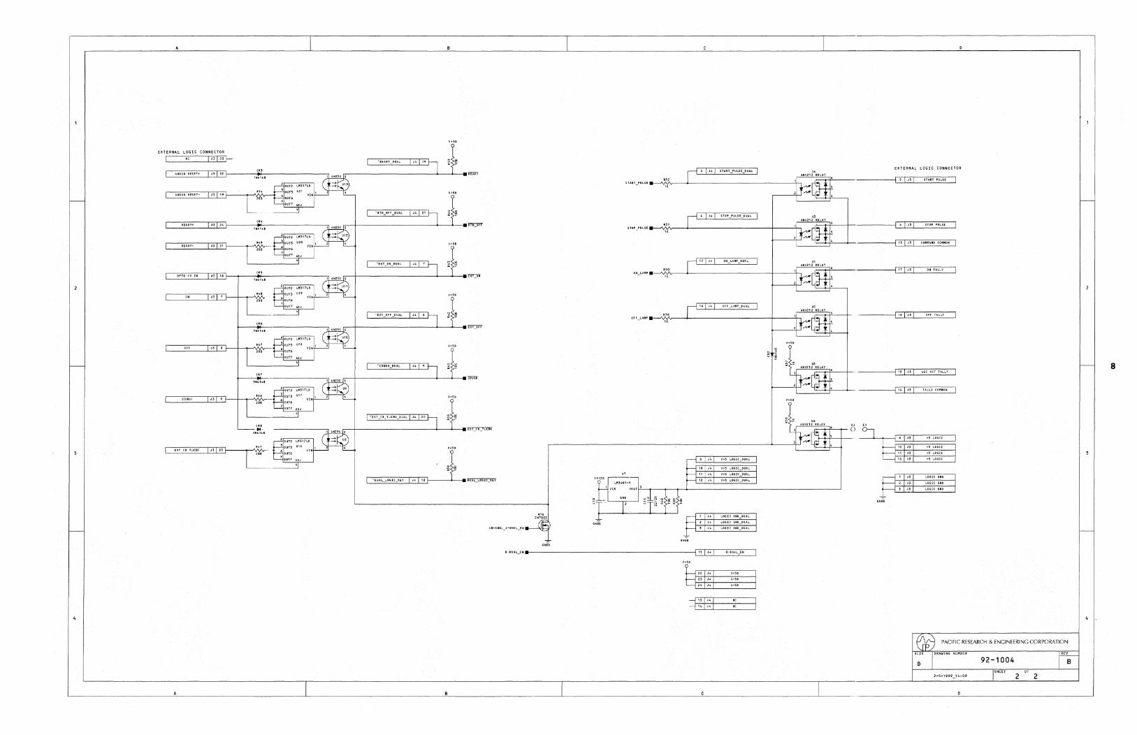
EXTERNAL LOGIC CONNECTOR
! J31 Z3 t-"READY_DUAL
START PULSE DUAL EXTERNAL LOG I C CONNECTOR
:::~ , I " I HUT PULSE
r.-------------------------4---~ ___ ~
STOP PULSE DUAL
I , I " I 'TOP PULSE r.--+----------------------4---~ ___ RfNyFf
In I J:S I CO"MAND COMI10N I
" LAMP DUAL -
I" I "I ON LAMP
:::~ r.--+----------------------~--~ ___ ~
'" LA"P DUAL -
'" LAIliP li 16 / J3 1
-r.--+----------------------~--~ ___ ~
I " I " I 8
r.--+----------------------~--~ ___ COUGH
I" I "I
]J31201
DUAL LOGIc KEV
'iNDO
B-OUAL_EN •• r----------------------------------------------jl~'~' II ~"JI=:::!:~Q~::::J
221J4
PACIFIC RESEARCH & ENGINEERING CORPORATION
92-1004 SHEET Of
2-5-1999_'4:09 2 2
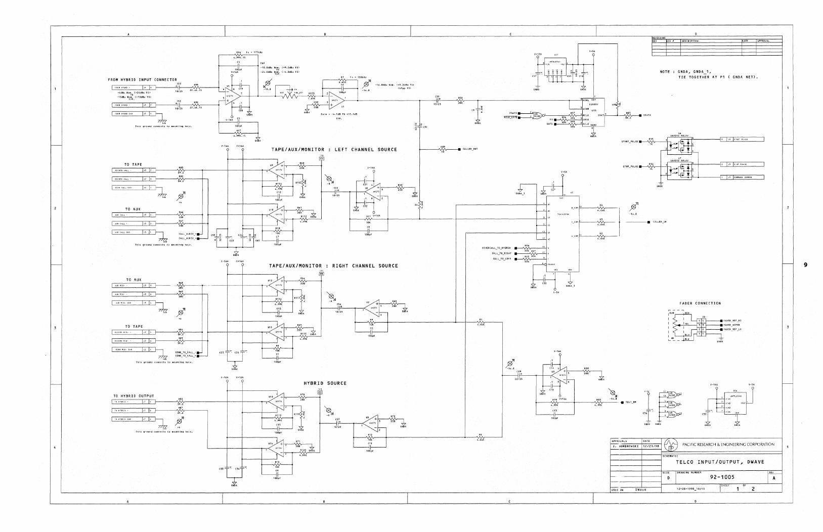
I I co. DESCRtPrION
146 Fe ,.111kHz Y+1ZD
4.991C:.n
NOTE : GNDA, GNDA_',
. ~t INV
~-10.SdBUNo_.(+9.2dBUFS) 180pF YO
Vt16A -24.8dBu Ny0.,._,. (-4.8d8u FS)
FROM HYBRID INPUT CONNEtTOR R7 Fc"133tHz TIE TOGETHER AT P' ( GNDA NET).
I .... " .... · +4d&ullo •• (+24d8uFS)
" -10d8L1 II~~;. (+IOd8u FS)
I F ~ON HV9~~ •
10'25
.. , 27.41(.11
i.~ 8 C19
ji/ -10.8
+ v
1 R123 l2.
6.65K
" 180pF
jlf -14.8
-10\..8dlluNo •• (+'.2d8uf$) (4VppfS)
L65K l- ~'----L-----------------------r-----~~~'~~----~"~'~--~----------------------------------~--~fAU~~'~~ lS9 31 OP27S ,; ..... ~ zot) 1 8 ",Ull VA+
.f~v\''''----=~+ '" 10/25 L tU331 R9A~ ~ "., - . - --
V-16A CS
Gain" -4.1d8 to +12.1d8 256FS':-:=~'~"~'0c)!-~=--:R<;o'~'¥."~~4 t R81 "I: 'AI" "" TYP. ~ ... 3HC02 196 MtLKSOAT~~SDAT"
611 A FS __ "V'",f'4v-;:~::'---'l3, LRCK 39.2
Tlli& g~ound conni!ch to _ountlng hole. ,SOpF
'" 4.99K.U
TAPE/AUX/MONITOR : LEFT CHANNEL SOURCE
TO TAPE ~ 160
~"~"~"~'~"~'~-====~"~'~~------if."1'r------r--------i-----i-------r-.• ~U9 OP11~ 200 5:8,: - 2 t--
RECORD CA~L ... 12 1
4.991:; I RCI1.D CALL $HD
59.2: R,,4 RI13 ! ... ,.
GNDA L-j:t-ISOpF
jlf 1--1------,
utO ~~h-__ ~.6A' __ ~ 1 -------I------I------~_r<::'y +11 '00
[~'"~'~"~"~-======G"~'~~------~2O~0r-----_t__!r 6~17~-·.Lhc,~ __ J·V'v,,~,~,,~,~ AUXCAll'" j! 3 R67 1'J 4.99K
200
'4
TO AUX
I ~ux CALL SHD
fhl& ground connllell 10 _ounting holll.
"
---j~J'"~ • +,
~~ ,"':, ~12:
ON, R1' V+16"
'OK
~
TAPE/Aux/MONITOR : RIGHT CHANNEL SOURCE
TO AUX ! AUXlliX-- lu 15
c
U~h' __ ---V'V'4V-----~ -'V'::,f':.,-----~---------+----+-------t-.,..< OPI7~ 2:00
.69 ----,
I AUXMiJ-$HD IJ314 ~ U3
---..J'Ip:"-'--__ -..... __ '::<~"' .m~ '. 200
R116 RI17 I-__ -"~"A. __ _! ..
----i~ 'SOpF
..& ",
TO TAPE __ ( ....... 1 us
... ,-------I----I-------..~"<'./' -:'Ir! 2:00 1; [~.~".~"~"~n~-~-====E'~'~'=r------~~~----_+_ir NOP17_·.hc,~ __ ~~~~~ 59.2 RI15 &NA
RHOU IIU'''' j2 6 US 4.99«:
59.2
"'T' "'T' T
V-16A '1+1611.
10K
--j];-
. ,01,'2:S _
"
HYBRID SOURCE
39.2:
I ~o HYDRU $HP
lhisgroundtonnects; to.ountlnllhoLe.
RI19 Rt1S :: I---WIr--+ ..
4.99K
'" 180pF
..& , .. 2:00 l ,ii(,
+ C3\
OTMERCALL_TO_BYBRU
CALL_YO_RI&HT
CALL_TO_LEFT
4.64K
64F$ ---""-'~'¥.04\r-.£.'~":':'~' ~"\"-"!-~
,i
,~~~" m
, " ~DO
B co~ 1"''------''i\''IV-----.,
" '_"" IL---_-"'..AA __ --4.641(
13 A1
604 RS7 " , 14S 604
60. --'< m,e<
~~'.:~ :.,,:: ~,16
ON.
200 1 ~ -14 ••
"' AQV212 RELAY
"'''-'"''' __ -'\.·",~f'v---~-'I'~I ~W iT""Yui-
"' AIilV212IEL"Y , __ 114 6
STOP_PULSE __ ---'\II"IIr-+~-----':h ""I~lli
&N~
FADER CONNECTION
I"" - --,
10d~BRED: I I J6
44 FADER REF III
1~IVEL33: FII.DER-WIP;R
I I 2: 2: fADER-REF LO I I - -I BLU 1 I
'-~ _ BLK uit
~ R19 Vt16A RIO
I----VVV-----+--------'VVV----- .. TEL1_"" 4.99«: ~
~ ~,c ----1...liicozP ~
"" "14 +rrr 200 ~
L------I-----t------~-;.c< opl76 _,-----"'.,;.;:"~O, ...:':::"",'--1 4.99K
'OK ." -----jt-----
APPj(ilY~LS DATE O\~ """J:""·;·::O.::.:"'''''O'''WS''K'''I-+':':'2~f:''2'''1f7:9:=8-l \Jt>y PACIFIC RESEARCH & ENGINEERING CORPORATION
SCHEMATIC
1-----1----1 TELCO INPUT/OUTPUT, DWAVE 10K
~: _, ______ + ______ ~SIZ~ I DRAWING NUMBER
-,- I 92-1005 OF
USf:.D II .. DWave 12-28-1998 16:45 1 2
I I I
- 9
-
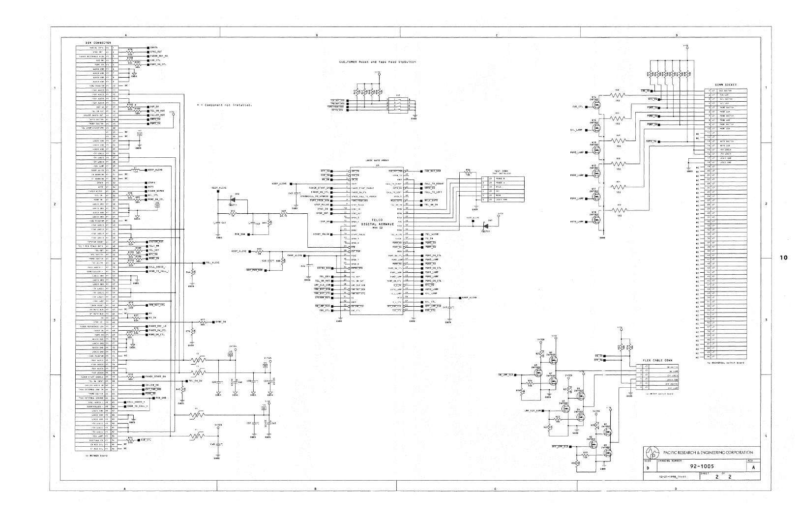
" t---l R1o.2 "
~-----~~~~ " PI 22~NC
LOUCGNDPI2sB .on
~16V ~UD!O PI :: t------l
TEL Oil our CALLER_OUT
" - Component not installed.
K.EEP_ALtVE
I :.. FC~2 R91
CUE,TIIIIER Reset and Tape Feed 1l1pSwitch
-.rr:m .. ---'-d = Cii'QV mov mry; 'O"IO"W
STAkT_PULse .. _J.-.!L.jSlART PULSE
OPENS
" m
U4
MAX 02
h!l_-I-__ ~
TEL_OM_IN
'EL ~L1YE f--"'--+-____ TEL_ALIVE
f--"'-+-____ F S_ IN ~ b"'-+--____ ~ ~ ~
KEEP_ALIVE .-IW~-,-----t-----------+-"-Q
C281-: R38
~:::::::::::B-::!" LOUCGND PI 57 GN~
" t------l '5YL06!CPI6G~ _12¥ UMP PI 61
CALL_AUDIO_~
SEND_TO CA.LL_-
GNOD
~ t=====~.,~ .. ~.~",~,,~,,=t:±:j~~~'r'--------1-+-~L--_~~~JA~" fL--.--~~ -U¥AUDlOPl ::1-1
TELQN,NPUT PI IG
cnLU AUOlO!N PI 81
I---~~.::....j" t=n-~--"':'::"::~I'-'-+':':'~R";'
R74
~--'::":::'::":::.!:.i~+':.:.'-{- Ne 200
L __ .:.:.c::.::..:::.:..Jl::.....L,::·...J~"
to IIOtHER board
v,
'''' 1" t "l~ ,ION" ON.. ON"
CALLER IN
K.EEP_A.LIVE .. .-----~+-"--_1 P6MI ON CTLI-"'-+-____ PGN'_ON_tTL
P6P13 LAP!P.I-"'--+-____ ""5_LA.N'
'PiiiD'i b"'--+-____ -.m:::<" P6~3 ON C'L i--"'--+--____ PGN3_01l_eTL
PGPll LAPIP i--"'--+--____ "Nl_LANP
PGM2 LA"" !-"'--+-____ 'GH2 _ LANP
~-L--''--'TnONou~ P6M2_ON_CTl !-"'-+-____ PGII2_0N_tTL
O_L~CTl i--"'---I-__ OIL_CTL
L ________ "_'-_tA_.-_"_' b"'--+-____ :;:_-~;~-CLk <:451" CUE CTL ~ b"'---I---II
GNO-O GND-O
027
OIL_LAIIP
... 2N7002
-If'' 2N7(102
'" Q15~
2MrrE 150.
PGN5_LANP~
." 2M7DD2
"",_"HP~
." 2M70D2
""-''''~
n::n1t---+-4 m:J1I
GNOD
V+1U
SHIM SOCKET
10
FLEX CABLE CONN to UNIVERSAL swftch board
PACIFIC RESEARCH & ENGINEERING CORPORATION
92-1005 SHEET OF
2 2
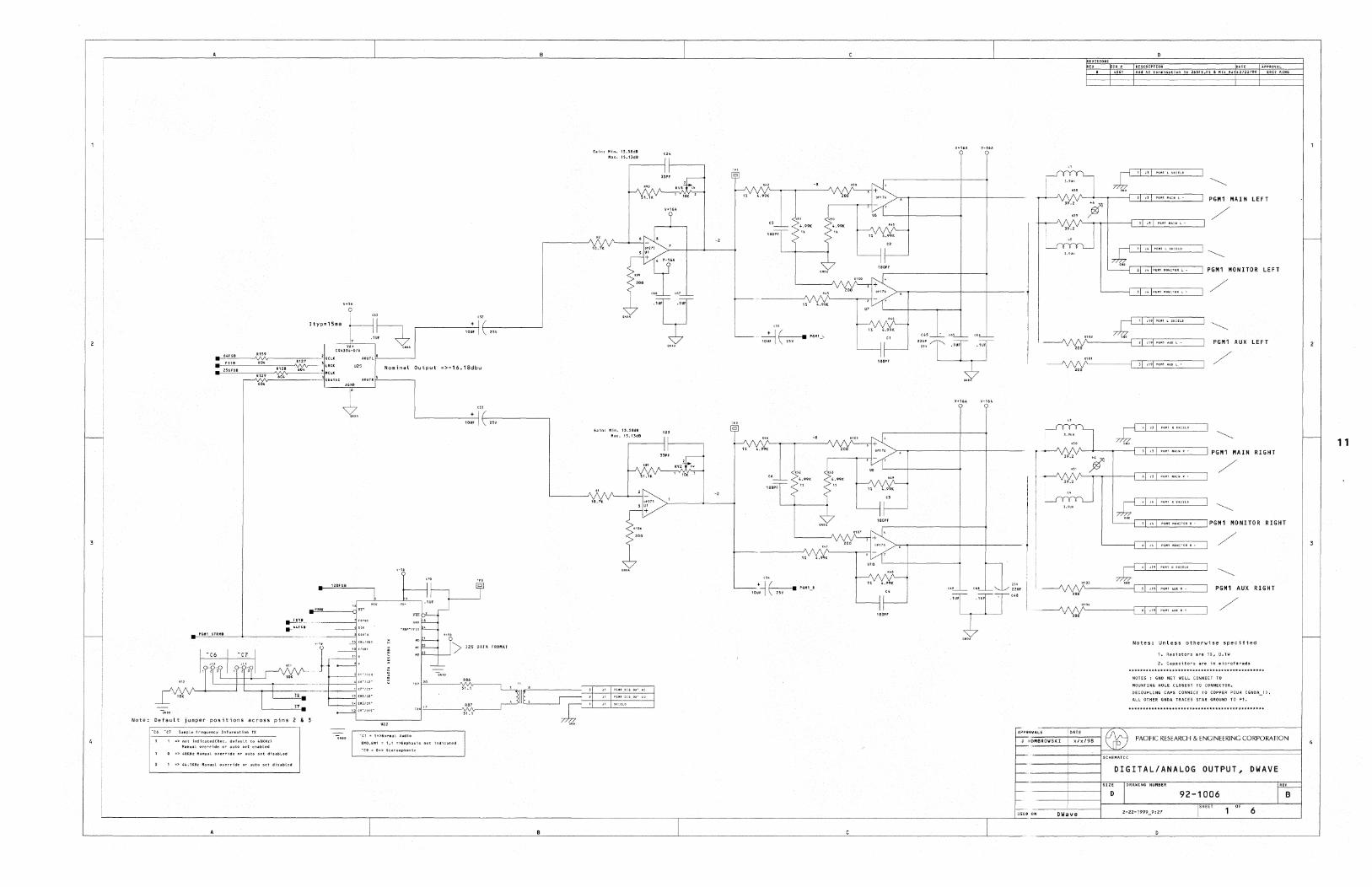
Note:
V+U
9 en
Ityp.15 •• HI ~ • 1UF
"
1 CS43:t~D/A GNU
• 64fSB ~ R127 2,SCLIC AOllTL'
fila 604 ~ .. L_U. U25 Nominal Output =>-16.18dbu "'''CLK
R12' 604 I SOHAl AOUTRI'-'-----,
604 A&~O
128FSB
--""""'-___ qiF
fOG'" STRMa
'P8 D
> I2S DATA FROMAT
De~:~lt jumper positions across pins 2 &
SaaplefrequencylnfornatioR JK
1 => not indicatedUec. default to 48KH2} H.mual override or auto set enabled
">48KNlManualoverrideor autD$etdl$abled
I =>44.1KHl Manual override or auto set disabled
_I--_~ a-H2'
,-'_----'t'C7 "/O'
\4EMOlc9"
\ C9"/C\5"
"Cl .. 1">Nornal ,\udio
£MO,.EIlI '" 1.1 ">Eaphash not indicated
-C9:0=>Stereophonlc
.. ,
B
6a1n= Min.IS.58dB "ax. 15.1:5dB
Gain: "in.n.Sade "1X.H.Uda
Jl PG"'.O;GOUf.,,:
Jl PG"' ~:G ,QU' LO
'" ----':J L------ "" L 'H1oUFl~ -
.J'f__ "" R
,ou~~ -
'" m'T~" .m 2SV •
...
'" 22uf
J ~IOflleROWSKI
USED Q,.
I DATE
EVISIONS EV COlt APPROVAL
ERfc KIliG 4361
PGMl MAIN LEFT
/
~'I"I,,",'mm ~
... r~-,-,---::c==:-:----, P G M 1 M 0 N IT 0 R L EFT 2 J4 PG"' IIOIII~OR L -
/
PGMl AUX LEFT
/
Notes: Unless otherwise specified
1. Resistor-II are 1%, O.1W
2. Capacitors. Il"e in- .icl"ofarads
******************"'*** .. ***+******************** NOTES : GiNO NET WI LL CO~NECT TO
MOUNTING HOLE CLO"SEST TO CONNECTOR..
OECOUPL.ING CAPS CONNECT TO COPPER POUR CGNOA_T>.
ALL OTHER GNOA TRACES STAR GROUNO TO Pl.
***********************************************
! x/x/98 PACIFIC RESEARCH & ENGINEERING CORPORATION
SCHEI'IATIC
DIGITAL/ANALOG OUTPUT, DWAVE
DRAWL NG NUfilBER
92-1006 B SHEET 1 Of 6
11
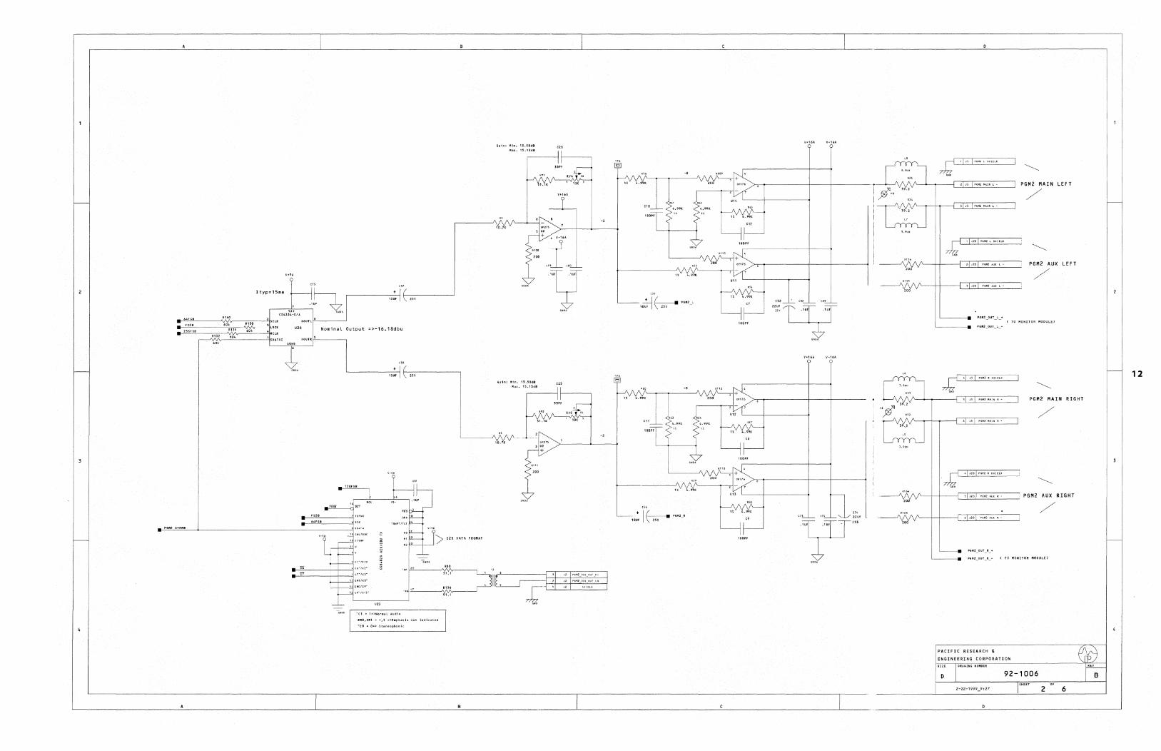
Ityp=15ma h ,~",.,;, ~
CS4334-0/A
AOUTL.I'-'---~
U26 Nominal Output =>-16~18dbu
AOUTR~' ___ ~
• 128FSB
POi!§" ~
FS21'1
'-l 1'Cel.fS9C
3 ~1 -IF CO
GNP,e
T~Npr IFe1 4
,,' , "' ' >
Mfn.13.S8dB "'ax. 15.13dB
Gain: l1in. 13.58dB Max. 15.13dB
'----tJ\N-10.11:
125 DATA FROf'lAT
"IT 4C6"H2- 0
IT 07"10-'XP (1',,-0 ------'\,:f, ,,_ ,~--,
n EM1tcS"
" E~OfC9" " <;9-fC1;-
-GNPD "C 1 ~ 1 ~>Nor~al Audio
EMO,EI'11 ~ 1, 1 ~>El1phas j s not indi cated
_ -_"_" 0"> "_"'_"_'_"_"_' _____ _
m
+I(_~"", ·-l~~- -
I m ~22Uf
'" --- + I E------II "" -'
10Uf 2SV
L:==_~ ___ ~ ___ ~ ______ ~ ____ ~ __ ~_
PGM2 MAIN LEFT
/
I I .20 I PG~2 L SHHLP
PGM2 AUX LEFT
/
11-- . ( TO MONITOR MODUL.E)
41 J> 1 PGM2 R S~;HO 12
PGM2 MAIN RIGHT
/
·I J20 IpGM2RSH;£LD. __ _
---,-----~ PGM2 AUX RIGHT
/
< TO MONITOR MODUL.E)
PACIFIC RESEARCH &
ENGINEERING CORPORATIO~_ __ ------"'r~-
D 92-1006 B
2-22-1999 9:27 2 6
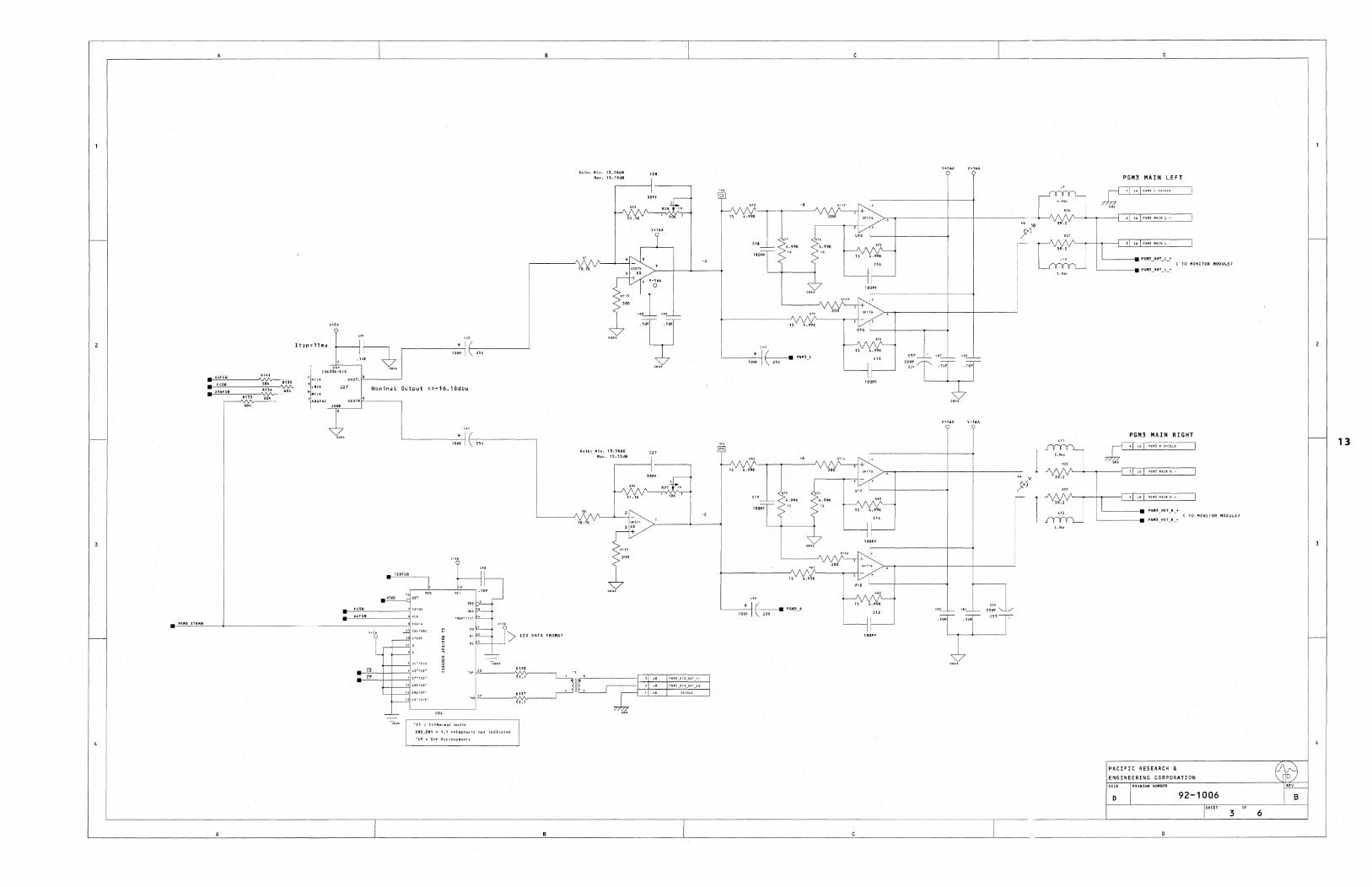
Ityp:15ma
RH>I ""
'\fV\r- R I SJ 64fSB 604 '\,I\/'v : '''' ~- ." .".~ AOUU S
Output =>-16.18dbu Nomina l
+ I 25V ~
+ 1"( .~ ""-' ~ lour
~ -Lvv~ - 39.2 +4 '4
j/'
PGM3 MAIN LEFT
J; ,1"1""",",,,,
P6M3_0UT_L_+ , TO MONITOR MODULE)
PGM3_0UT_L_-
PGM3 MAIN RIGHT J; ~I -;-;p", e ;"'~
PGM3MAiNR-
P6M3_0UT_R_+ ( TO MONITOR MODULE)
PGM3_0UT_R_-
RESEARCH 8. PACIfIC CORPORATION ENGINEERING
CWIItlG NUMBER 92 -1 006
SHEET
3
13
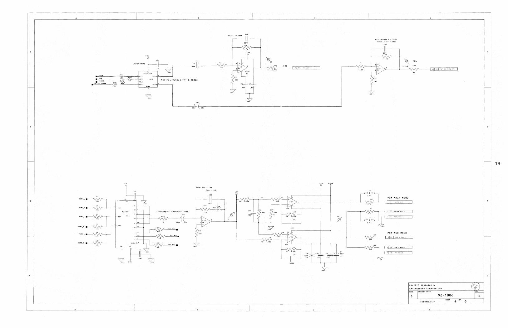
• 64f$B
.' FSS • lS.6fSB
•• I-'C",UE"I-"""-'-!'!!""'",~_~ ...
""-'=:l '" '" P6"1_R _
"
". ~
Ityp=15ma ~
~, .. ";'-7.. 10UF
.162 CS4334-D/A
~ .. 1'4~""R~,,~.--.22 SClK AOUTl!"·-----....J
"'~,~;6D~'~4·--'J3 liCK U28 N' 004 4 MClK omlnal Output =>-16~18dbu
~,-___ -,1 SDATAt AGNO "OUTR'f·'-----~ ,
Fc=1/C2*pi*5.2K*22uF)=>1.39Hz
'"
Gain: P1in. ~1. 7dB
lIax. +l.SdB
4.12K
~"" $200
,7
Gain: 14.16db
II
CUE ------1~_,,~I_,_,~I~~~ __ ~
'" ""T
Ga i n Nteded '" 1.38db hlu., 6UM" 1.45db
PGM MAIN MONO
! 1 J9 1 P~II liN IIONO •
-I J9 I P~" SHIELD
PGM AUX MONO
r ,I J9 1 PGJII AX 11010 +
-1 ·1 "I", .. ",",.
TEL
PACIFIC ReSEARCH &
ENGINEERING CORPORATION
6IZE ORAIiINGNUIIBER
o 92-1006
2-22-1999_9: 27
14
B
4 6
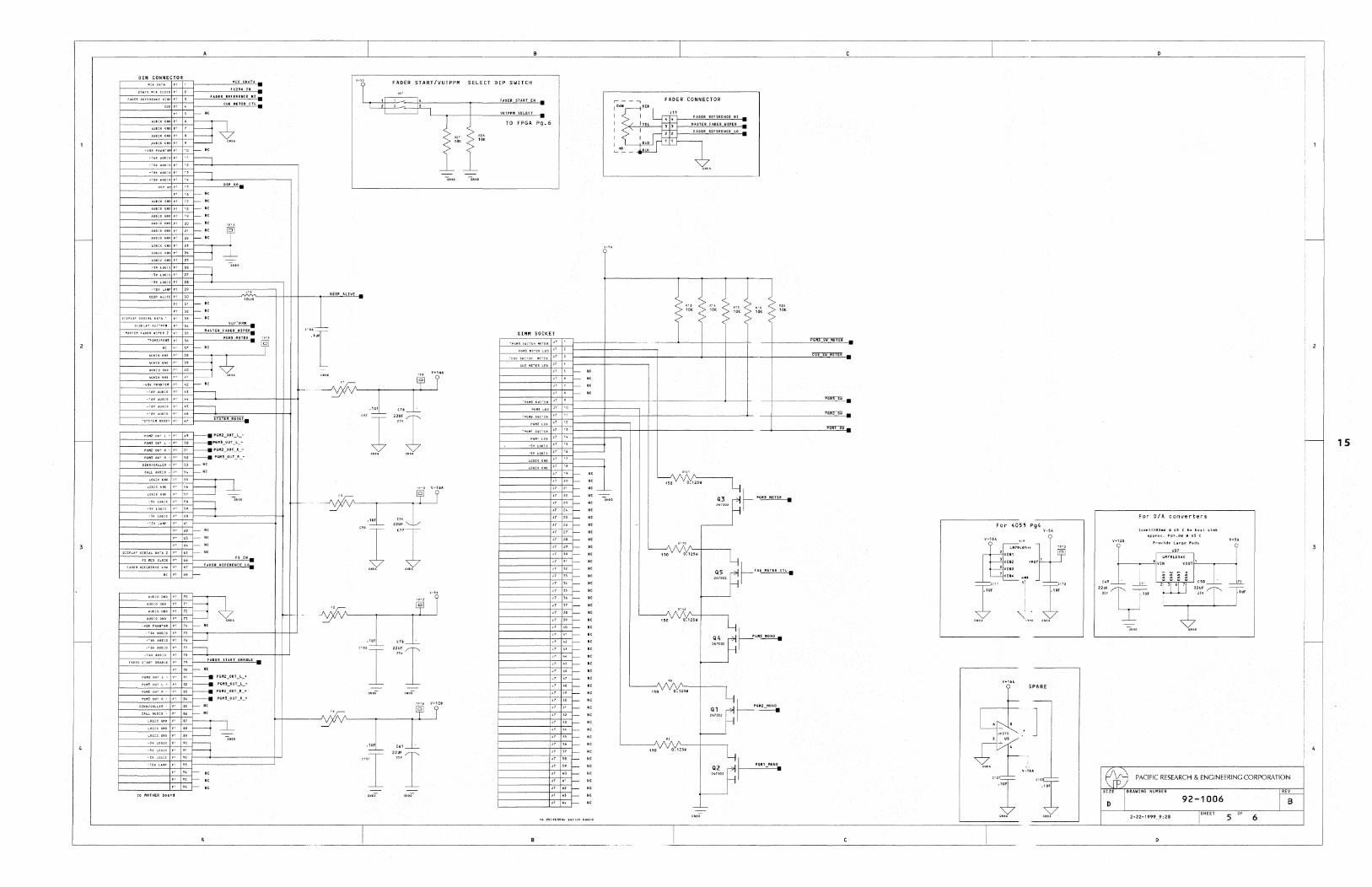
4
OIN CONNECTOR lUX $OATA
2S6FS!'IIX CLIlCIl P' 2
FADER REFER.£~CE KIGK PI 3
fS256 III
FADEl REFERENCE HI
CUE JIIETER CTL
p' S t-- NC
AUOlDGN.P\ 7 AUDID6N.P\6~~.
~----~,"~,,~,~ .. ~,r.,~.~,-t
-,6'; A.UOIO PI 13 ----,
-'HAUDIOP' '4
p, '6 f-- NC
17 i--- H1:
~----~~~~~,.:I~ "' ~----~~~~i7.,.:-1r- "'
20 r-- Ne
~----~~~~~,,-[-- " A\lOIOUDP' 22 _IIC
DSPG~
LOGICGNOP'2'p
LOGlCGNDP' 24 _'_
LOGH GND P' 25
GUD '5VLOGICP' Z61! ·5¥LOGlCP' 27C1 ..
,SYL06ICP' 28
"2YLAltPP, 2'
" 3' I-- NC
P' 32 I-- He
DISPLAY SEI(UL DATA' P' H I- NC VLlrpPJII
~--------=-~i7."-[r- ., AUDIOGIIDP' HI
~-----"',""',,-, ",,:-. ~t:-t==1 Vol. ~----.~ .. ".~,"~ .. ~,,~,r.,7'~":-r- "'
-\6VAtI.I(tP"3~
-1(oYAUHOP' 4511 $UTEII RESE!.
pi 62 I- IIC
P' 63 r-- Ne
P' 64 r-- He
Dl$PlAT SER.tAL UTA 2 P' 65 r-- IIC
.. ~
74 _IIC
P' " t-- lie
P' '5 r- He
P' '6 r--- lie
to .JiIOTH£R bOilrd
v-so FADER START/VU!PPIWI
r '~4 l
j '" '"
GNn
tc.EEPALlVE
+ .1L1'
." V+16A ,jNDD
",f J .. --YIN' f-..
.1 mr-r '"
GNU 6MOA
TP'O V-16A
--YIN ~ J .~ 2:~;1
'1 "J .l¥ "r
.1UF ",1 'I '''I '"
GltOD GnUD
../\ .¥ j" .1 , .. I "'r '" "1
IINDD
SELECT DIP SWITCH
GNn
TO FPGA Pg.6
SHI" SOCKET
H S t-- Ne
Jt 6 I-- Nt
-- " ~----------~~~-- "
J7'S_
~-----2~~t,"i7.,,:-1 _______ " " t==::J ~7 '9 r-
f-------t.,,-j-;;;-Jr-i------t;,.-t;;-Ir-
J7 22_
I------t;-,.-t;c<t-I------t;-;-t<t=
J7 26 I--J7 27 t--
f------t-;;-l-;;-IeI------j-,:;-, "t; .. ;;-[l= 1------t-7;-i;;:-Iri------t-7;-1-;:"r-
J7 n r-J7 34 I--J7 3S I--J7 36 r-
f-------+;-t;;;-l~ a 39 t--
f----------~~~
I------t;-;-t;-;-eI------t;-;-t;:;-l=
t===========~,;,~ .. =1~ J7 47 l-
e-
t==18"E,,~ ~--------~,,~,>l, ~
~7 53 _
e-H 55 I--H 56 r-H 57 I-
::1 " "' -
GNOO
I A A"A'/ ' '--_--, ~DVVOy125"
Q3 ~.~
-" A RHO /'--+ ____ --, 150 V Vo,usw
I ,~,~" ~ L,,~ w,1
~ARA/IL~ ____ ~ ------ ';0 V V 0:'12511
Q4 ~'"~
I A A"'A A,----+------, ~OVVOy1~$1I
"/ A .... __ -+ ____ --, O.125W
:~::~ ~2 ~ ~--------~,,~,,;-l==
For 405:5 Pg4
V-16A W : ::::,;':;":.", ';;' 6 VlN3
7 VlN.
II' .r V+16A
SPARE
J
For D/A converters
hont">8S.A iii 45 C tlo hut sink Approx, Pd".6W iii .S C
V+1211 Provide LilrgePads
PACIFIC RESEARCH & ENGINEERING CORPORATION
REV " .. -- """ ~ "':lUF '''''l'' t:=====:t~" ~" --
'- " SHEET 5 OF 6 l~------------------------------------------------------------r_--------------------------------------~~~~:'~~~----------------~--~':-"~;-~------------------------------_:--------------------------~====r=== .. = .. ===- ~== .. = .. ======~ __ _l _______ 2_.2_2_._"_"~-~'_'2_8 ______ 1_ ______________________ ~ to U~lHItiAl .wiu' board
92-1006 B
15
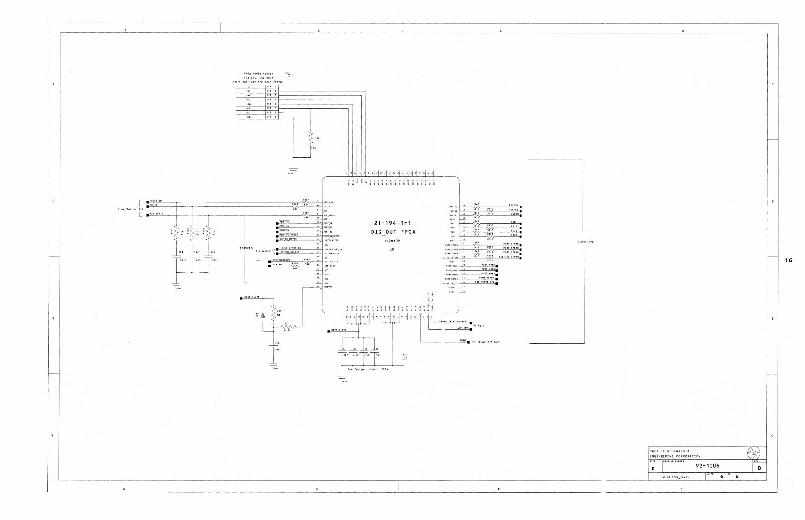
I
-
-
-
I
FPGA PROBE HEADER
fOR ENG. USE ONLY
DON'T POPULATE FOR PRODUCTION
J18 6
J18 5
J18 7
I ~ '" ~R25
--
R168
INPUTS Dip Switch ::::11-=""-"-"""-___ -"--1
R166
21-194-1r1
DIG OUT FPGA A42MX09
U9
One Cap per side of fP'A
I
~ 39.2
RUO
39.,
39.2 RI51
Nt" f-2.!L PGMl PION!) f--'-""------""-'-='II
P6M3 IIONO f---'-'------"""-""""-P6113 II£T£R f--'-'----='-"'''-''''-II
L---____ . ------" .... "-."-11. For U40, Us' only
0
,
-
2
128FSB
64FSB
FS2B
FUB
OUTPUTS
f---16
3
-
4
PACIFIC RESEARCH &. ~ ENGINEERING CORPORATION ~c
SIZE I'"'''' MU'''' ~
D 92-1006 B ISNEET 6 " 6 3-'0-1999_15: 34
I 0
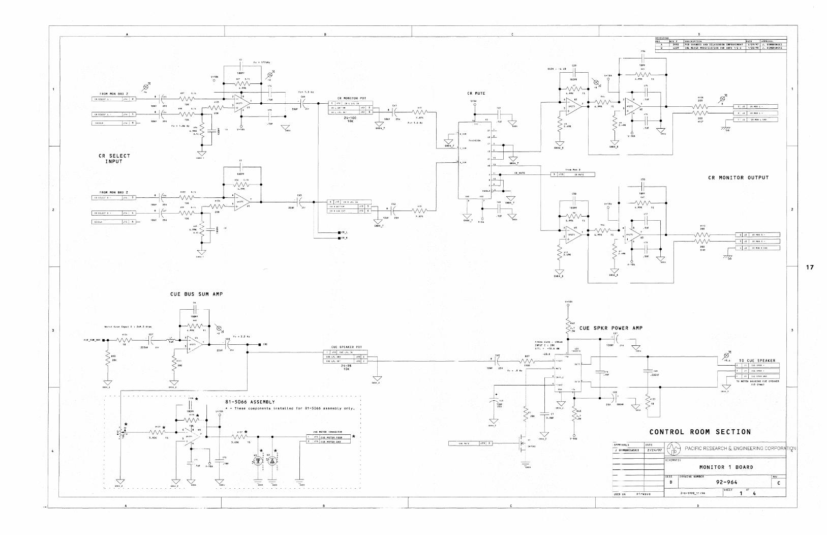
FROM MON BRD 2
I,,,
I", I
11141
CR SELECT INPUT
o
f!! , 1
+
I ,
1
+ 1
1
'f-
FROM MON BRO 2
I,,, , 1 ~===r;:~~+ I~
I,,· I 4 1
IJ14 I 6 f-~=::EEJ-~I~n'" '~'lJ!
V'
CUE BUS SUM AMP
"" ,,,,,,,,,,11 1: "" 4", ~_,4':'"," ~'" eo-"",
'"'-'""-'"' ~~ - .
~'::." '"'' f'" <:'> .. " C,
~ '"
'II>~ *
4 112 CR R LH
~v. L GNDA7
"-'
24-98 10K
II 81-5066 ASSEMBLY i * - These components installed for 81-5066 assembLy only.
I'---..... -:_~~ ~, --+---1\ Rn! /'*~-t"""-11---------i'=4~"''="~:;::~' ";-;:.;,:~:'~:~::~:==1 * *
"}-,,/ J16 CUEI1ETERGND
"'1 ' l' ""r
* *
1 G~"O G"DO G~bD
CR MUTE
v
J'~. I
Ti Li
4.' CUE SPKR POWER AMP ."
REVISIONS
REV ECa #
RIIO ,eo
CR MONITOR OUTPUT
41 J21
fIXED GAIN -------"( INPUT Z : 201(
AlT. = -18.6 dB
I"~O R27 -20.6:,'" ______ C-.j, 1 I -INVI
1501( , ZSV 2 : ~U' E I ~ TO CUE SPEAKER
, I" 1 ,",m.-
~---~~----ll "'''''~.
CONTROL ROOM SECTION
APPAN"LS~ __ f.:-'~_--I
J IlfJMIJROWSKI 2/24/97 PACIFIC RESEARCH &. ENGINEERiNG CORPOR ! IQ\I
SCHEMATIC
-----l----...j MON !TOR BOARD
SIZE [)RAWING NUMBER
D 92-964 C SHEET OF
USEO O~ AirWave 4
17
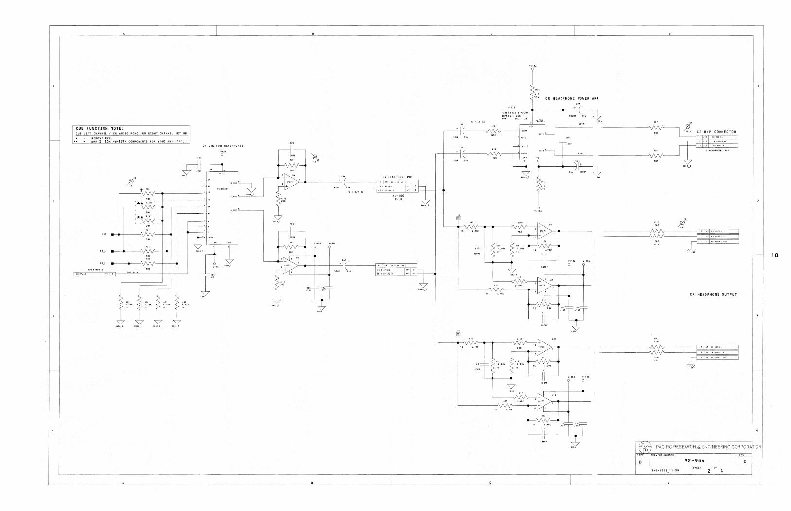
CUE F UNCTION NOTE: SUN RIGHT CHANNEL SET UP LEFT CHANNEl I CR AUDIO MONO
CUE 140 AND ,'4'. =~:O~E ~~~. (6-255) COMPONENTS FOR R
CR CUE FOR HEADPHONES
F,l --
IItOM J! _. , ,,' *
74HC4053M
C_COM
'" -11.140
A_COM "
"
'" CUE
CR_L
CR_R GNU_'
frollMona
I'" '" . CUE/-ALI(
h~O~
~ .. , 3.3211:
V GNDA_2 6ItU_' e~DA_2 ~IIPA_l
10UF 25V
10UF
GNP~_'
'"
-20.6
FIXED GAIN 1 +30d8 INPUTZ: 201(
ATT. '" -18.6 dB
2 MUTE
/\ ./\ ___ +-,9 -IIIV2
1.7
." CR HEADPHONE POWER A"P
1 ----+C2E-1
100UF 25V '<Z~ '" 'U2616
C2f±.-.:.---~ ... -,-,'. "'" ~.
CR HIP CONNECTOR
~m ff' '00 " ,1,,1,,"""'-
-------IVV'v=====c~,I~,~,I~,,~""~" ,~-~~ -------~rvv\I' ,I "I,,"""' '"'
~ 18
CR HEADPHONE OUTPUT
~" ;
20' J=±SI~"~I~"~"~"~"~'~.~~~ -------IVV'v. ____ { ,I "I,,"""" --------~ ~ ·1 "I,,"""""'
PACIFIC RESEARCH &. ENGINEERING CORPOR ION
REV
92-964 SHEET OF
2 4
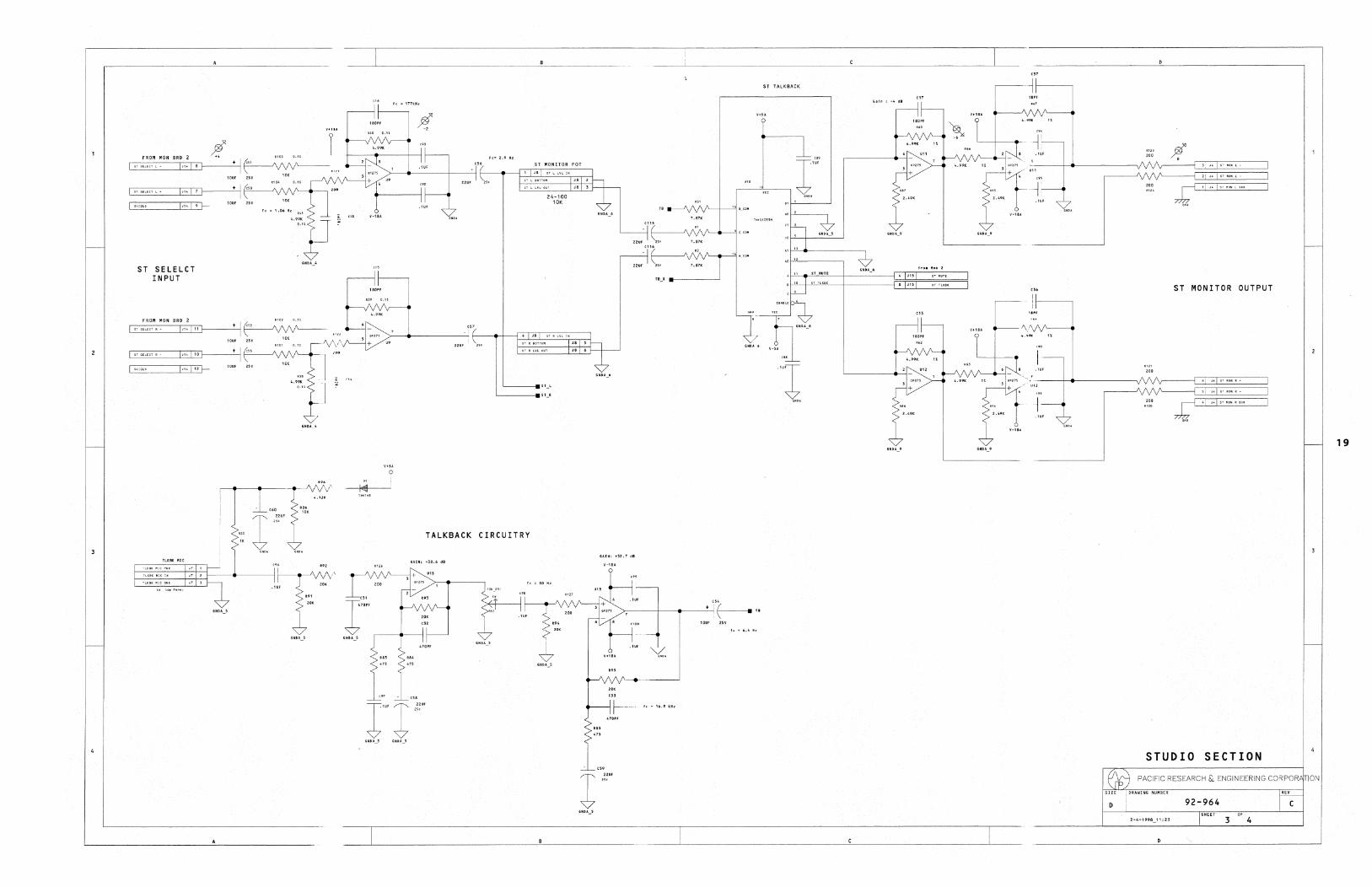
J! I ~=:::=EI:D-----~+ I ~""
ST SELELCT INPUT
IOUF 2SV 10K
FROM MON BRD 2 R102 o.u
'-;-;-;;-~:EJ~~+ I~/\/\~" ~ IlI'[11[ '~VVV---·
1DUF ,.,
E;;;;;::;=~I"~' I~"}-I -~+'-11 f"-'----'\
I
J ]m]lzt---
l~\
Teo:", ';~,
~'" GNU GNU
,
o
l<!ill
TALKBACK CIRCUITRY
51 MONITOR POT .. STi.LYL!N
24-100 10K ,
o eo" 6NOA_6
ceo"
Z2UF '" C116
14 A• COM
GNDA_6
$T_l
Sf_It
~------4---~~----~+~:'( • .. '"
Yo.
en
f--470PF
ST TALK BACK
1: Itt.5 ;f
'" 200
r 21 J4
-1; J.: 'I J41srftONLSHD
GNDA_9 GNDA_9
4 '" ST MONITOR OUTPUT
1\...
I
'"1 It •••
2.'
," " STMONR_
; " STIIONR-
1 J; ,I j41STHOMRSHD
19 GNDA_9 GHDA_9
STUDIO SECTION
ION
3 4
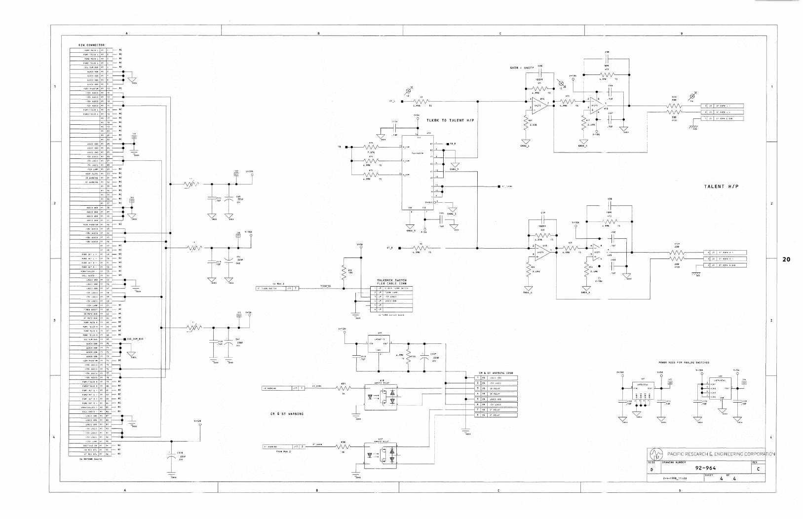
DIN CONNECTOR
1'6"' TELCO L 1'1 2 f-- Me
P~M2 HLtO L PI 4 f--- Ne
::i~
PI 20 I-- Ne
" --!'--:--J
!! i-- Me
r---~~~r_+,~,~~ " 1'1 33 l-- Me
PI 35~Me
PI !6 r-- Me ~ r------~,~,+,~,~~ Ne lL
_IaYAuDto PI
PI 48 r-- Ne
i-- Ne
"",,,,,,::a l 58-1~
AUD!OGNDP';~~ f-----:::::=-=-+':'--f:'~d 'Y.:'.
84 i---- Ne
"
I" .. ·""
CR & ST WARNING
IsrwAltNIN6
7.87«:
4.991C
GAIN
ST_' ---------'\f\IV-------+------------<~-I 4.991(
TLKBK TO TALENT HIP
~,,,
('-------'j-
1-'-'---.>--_____ --+ ____ S~ "LUK
~ 'T ""-' ""~
STR~
TALKBACK SWITCH FLEX CABLE CONN
e117
22UF
CR & ST WARNING CONN
'"~ ~E
~-"-----f-----: J~; iii:: § --== 8 J6 ""iNtD
en
r---I t------, : I,P'
~'" f'2.49K
! V-II"
V GMO,,_4
UPf
i,
-1 .1UF
'"
-1
RUI
200
R129
200
200
TALENT HIP
r-1 .1 JS 1 ST HDPH RSHD
POWER REGS FOR ANALOG SWITCHES
92-964 SHEET OF
4 4
20
10",
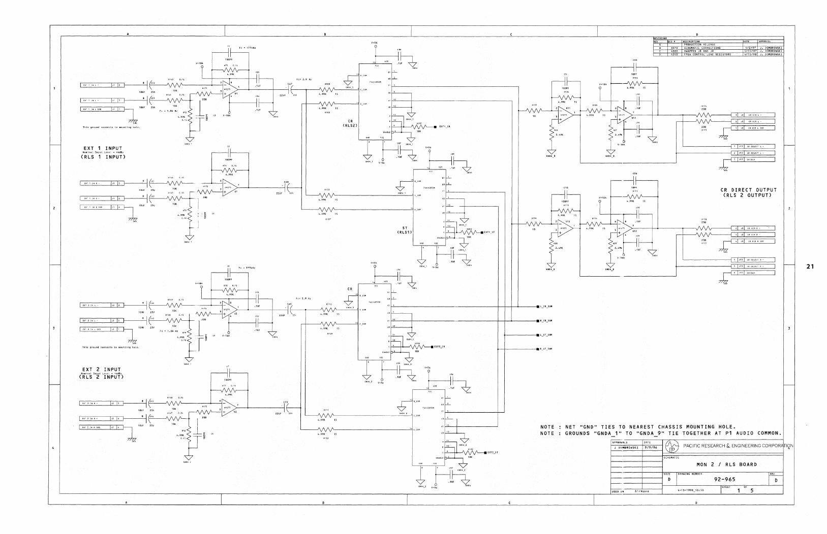
~~=:=EI,,;::r1 ':::JI-~+ I 1-----'\
10UF
~~:=E::I" EI' J---~+ 11-----'\
1""' This ground Gormects to .ounting hOlle.
EXT 1 INPUT NOllina L Input LeveL " ~4dllu
(RLS 1 INPUT)
GI '~"'~'"'=' =:=E1,,;::rI;::JI-~+ I~
+ I
1""'
r;::-~=:E~}-~+ If" . ;'~A';' ... 1-",-''"'· I" I' 1 '~VVV-T"
~~~IE"EI'f---~+I~-J\
1,,1, 1""' This grQund connects to _"unting hOlle.
EXT 2 INPUT No. ina L Input LeveL " ~4dBu
(RLS 2 INPUT)
GI ,:c::,,~, ,"~, =. =::EI "~I=' }-I ----.:+~I '-"" __ -f\ 25'1
~::::::=::E;:::E}--~+ IE ....... ;'~ A ';'-'-"'- I" I' . \~ V V V - ..
I" I, TO.
f'--~---1_
1'------1-
CR (RLS2)
1'--------------'1 -
1'-------------"1" '.CO"
ST (RLS1l
1'''' , R~OO
~EXT1_ST
f-l----------------------+-I-f--+---. L~CR_SU"
pL---f---------, .. --------+-I-.l.-----.R CR SUM
<-+-----__ 1< ST SUM
NOTE NOTE
'" , PRODUCTION RELEASE 3979 SCHEMATIC CORRECTIONS 4020 SWA.PPED J8 AND J9 4248 FPGA. CONTROL LINE RESISTORS
4/2197 J. DOMBROWSKI 5/15/97 J. DOMBROWSKI 4/15/98 J. DOMBROWSKI
R174
'00
R17a
200
CR DIRECT OUTPUT (RLS 2 OUTPUT)
NET "GND" TIES TO NEAREST CHASSIS MOUNTING HOLE. GROUNDS "GNDA 1" TO "GNDA 9" TIE TOGETHER AT P1 AUDIO COMMON.
J ()(l"BROWSKI 9/9/96 IQN
t===========t=======~'~C~HE~MA~T~I~C======================================~ PACIFIC RESEARCH &. ENGINEERING CORPOR
1-----+---1 MON 2 / RLS BOARD
SIZE ORAWING NUMBER
D 92-965 D SHEET OF
USED U~ Ai rWave 5
21
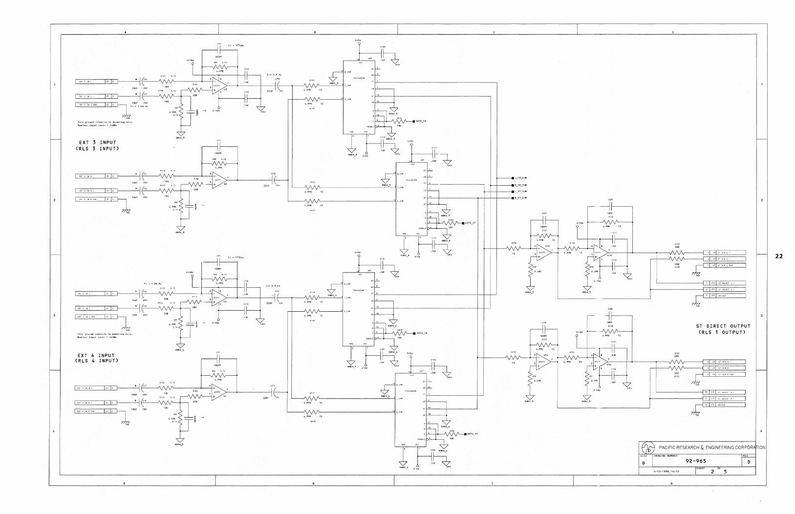
1
1
In I, + I 10UF
113 I, + I 113 I, 10UF 2.SV
~"'''D6",
This ground ~onne~u to .ounting hoLe. No.inaL Input LeveL ,,+4dBu
EXT 3 INPUT (RLS 3 INPUT)
113 I, +
111Uf
III I, +
Ij3 14 1""
This ground ~onneGts to .ounting hole. NO.inaL Input Levl!L " +4dBu
EXT 4 INPUT (RLS 4 INPUT)
IJ4 I, +
10UF
IIIi I' +
£P 4 1" R·
EXT41"I!:SHD I .. I· 1''''
I
I
Fe "'.06Hz
I
I
1800PF
Fe " 177kH~
flOPF
V-I8A
1'------"="----'\ C co'"
/'----'-1-
1'-____________ '_"_"_-'---14 C_COM
V+5A
('---==--,\ ""
'''~'
C10l
h-' . '~F '7
GNU
('-_____________ '"_"~-'-'l4 C_COM
('---------------414 A_COM
V-SA
C114
h-' .'~f '7
G"D~
'1U~ •
-1f-----ST DIRECT OUTPUT (RLS 1 OUTPUT)
92-965 SHEET OF
2 5
22
ION
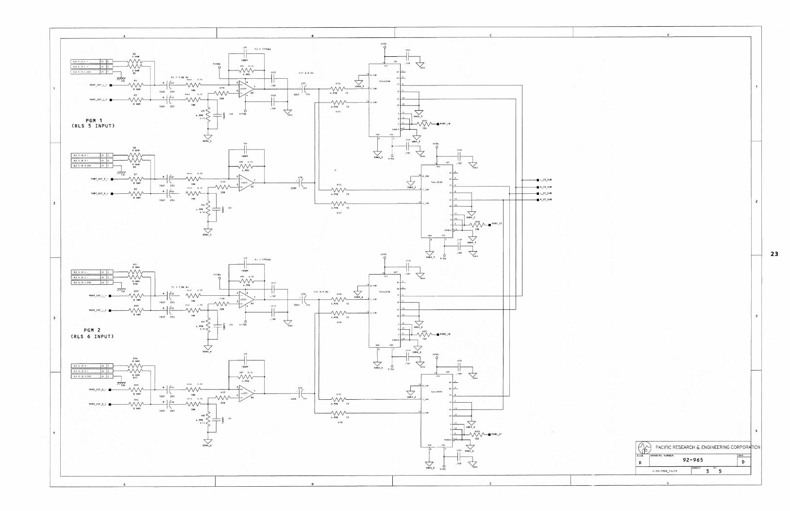
I RLS 'S IN L S~-o
PG"'OllTL+ .... __ -''\
PGM 1 (RLS 5 INPUT)
IltLS5lNLGHD
PGM 2 (RLS 6 INPUT)
..
V+UA
4.99K
4.901(
·"hz. f'L------------.::"'::;':=-.::' -'I c CO"
~+_--. R CIl SUfi
f\------------~ _
C127
~-' .1~F ~
GRDA 23
"~'
('-___ -"1' A to"
'1U~. 1\1"-____________ ---":.:"""-""-44 ._.O~
"
4
ION
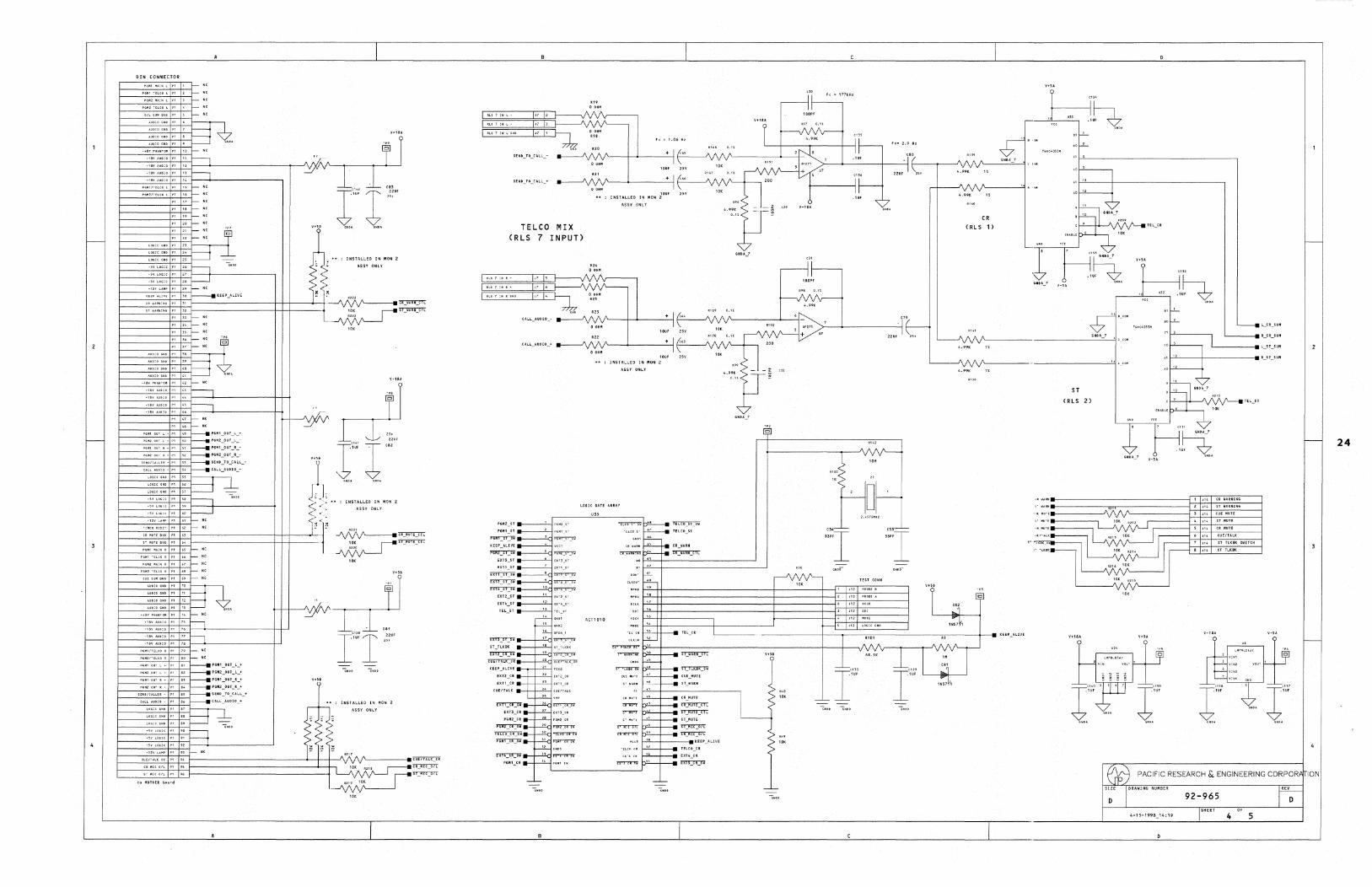
DIN CONNECTOR
PG~1 M~l" ~ PI , f- Me
e-_~~~~~~'~r- "' PG"i! IIAIN l PI 1 f-- Me
" r- Me s r- Itt
-IBYAUOIO PI :: ---,
e--~~~~~~::~== :: e------~~~~ :: e-_____ ~~~r- "'
r_"' e----,,-,,-,-'"-.r,~,+=,,~~ :: _~
~06:tt ~N~ pI <4 P ~ 2'~ 6ftDD
~ e---~~~~+'~'~r_ "'
11+18.1.
A -'A I'.;;j
INStALLED IN filiON 2:
ASSV ONLY
J0r--KEEPALIVE 222
r:=:j~E~~====m===t-~n::vrn::m r:: ~n:vm:m f------f:'--F-1~ :: 10K
e----.-.-D!o-,-.. +,-, +,"-.~E:: j e----.~"'''-,,~,~ .. ~,~,+,''-,-r---1 ~
'"",'" " "py..
-U¥AUDIOPI45~
-IIIV AUDIO PI ~,
LOaICGItDP1S7~~ " r---, "" .. I-----l
e---~~~~+="~e- "' 62 r- Ne
e--~~~~r-+'''-'~-- "' f--~~~~~+'~'-1== ::
e--~~~~r-+:"-:~== :
-1aVAlJOlOPl ::h.
~rr!} T','~; I'" ,.,. ¢
I "" "" r;J ~ .>" INSTALLED IN NON 2 < __ - ASSY ONLY
v~; R221
~CR_"UTE_CTL
!~:a r-- IiT_MUTE_tTl
~ 'OK
INSTALL.ED IN '"'ON 2:
ASSY ONL.Y
B
L-___ ~I_,,~I_,~~
TELCO MIX (RLS 7 INPUT)
'" OOHII
'" 0011"
10UF INSTALLED IN /liON 2:
ASSY ONLY
10Uf
10Uf INSTALLED IN MON 2
ASS., ONl.Y
LOGltGATEAltitAY
PGII2_n •• ---'-1 PG.!l2 aT
P&III_$1 ::.---'-4 PSi'll &T
pfHn_sT_sw • __ -"-'q P6!ll_Sr_sw
KEEP_ALIVE •• ---'-4 P&M2_sf_sw. 5 ~
EXJ3_ST:: E:tT3 Sf
EXT1_ST __ --"-jUri aT
U35
4.9\1K
'~I GJtDi'"
/'------'i' • ,,'
CR (RLS 1)
4.9\1K "
~ ___ --"1':\~
::;:-:;-:: ~ ,: ::::=:;=:: E;rz=sr :: EXT2_H EXT4_ST. HT4 H
TEL_Sf •• --""-i TH ST
~(; .. o,
~GND2 .!.L OPEN'
"::::1:: ~~~-VYY-~'~OK R§ "r" Cj '----liI*--+
r-- 5 '~~1 ACT1010
~ .-+-~"-q rm::rr:rv ST_T~KB; =._+-"'-1 ST TUaK
UTz_clt_sil ._+-'-"'q ~ CUEITALK_CR 20 ~
KEEP_ALIVe .-.--+-"-1
1-"-_1-__ Cit_illiTE
n"'IItI"'r' ~
f"""IItM' 1"TJiUTDTI
..,..."."". P'"'-I--- rr:rn::= ~ ~
TELCO_Cit
i-"-t--II EXT4_ClI
!'l"'T'tT"1V nn::rov
1'------ ~------+_-=::r'==:;;;===='-------,,---+- KEEP_ALIVE
v+SI)
10K
<
V+5A
4-15-1998_'4: 19
Cit W,I,RNIN&
STWARRIN&
ClIEMlITE
st IfUT£
eRIiUTE
(UEIJAl'-
¥OUT 1
r r 92-965
SHEET OF
4 5
24
ION
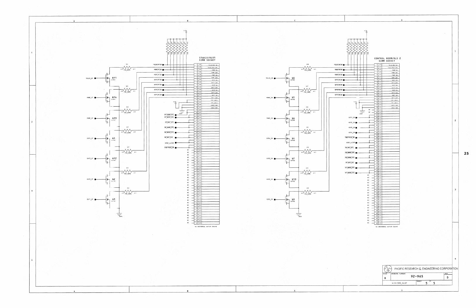
r--
-
-
_.J' I ~~I"~~'
I
I I - "" .'.--~\,'-,--,--~
---11·n' ---
---1~~~ ---1~I'~~
-
--
I
STUOIO/RLS1 SIMM SOCKET
•r----r=r-~=t"~"~'t======j KEEP_HIVE 32 J1()
~3'J10
~-----:1-1=t,,~,,~,~====~ :~ =f-'::+:::.::+-----__1 NC _ H Jl0
"' _1-',,:-I'-',,--,t------1 Ne _ 39 J1U "' _f---O,,+,,:.:,+-------1 Nt _ ., J10
"' _1-',,:-1'-',,-,-,-1------1 Ne _ 43 )10
"' _f-',,'t. -'-,,:.:,+-------1 Me _ 45 JIG
"' _1-'":-I'-',--,,t------1
:~ :1-'::'+-'::-':t------1
:: =1-':::-I'-':,--':t------1 Ne _ 51 JIO
"' _1-',,'+-',,-',t------1 Ne _ 53 nQ
"' _1-',,:-1. -,--"t------1 MC _ 55 J10
"' _1-'"+,"-,,t------1
:: =f---O::+:::-:::+-----__1 Ne _ ,9 no " _1-',,+,,"-,t------1 NC _ 61 Jl0 "' _f---O,,+,,:.:,+-------1 NC _ 63 no "' _1-',,:-1. -,, __ ,t------1
to UNIVERSAL ~witch bOJrd
I
I
Q8
'" r----I-,-~~,~/.
---1L .. , r---+-,-_,v~
---1~. , '---+-.-_'~~I
I
CONTROL ROOM/RLS 2 SIMM SOCKET
';"." " -----+-+
~.
r-- 27 J1'
EXT4_CR .----1-i=~,,~,,~, ======1 129J11
~ ·---~-t,~,~,~"t======1 ~31J11
KEEP_ALtVE -- ---J..~t,~,~,~"t======1 jJ3J11
TIJffC":OIT .. ---~-t,~, ~,~"t======1 1 35J11
CR_MUTE_Cn It- ___ J-_p,~, ~'~"1======1 1 37 '11
CR_WAhI_CTL ... ___ J-_jj,~, ~,~"t======1 ! ~9J11
ST_PHC_OIL .. ___ J-_p,~, ~'~"1======1 1 41 "1'
STYUTE3TL ... ----1-i=~,,~,,~,======1 r-" '" Sf_WARN_tTL __ ----:;;L-{::,G:, ~,~"t=====1
Nt _ 45 '11
"' _1-','-+, -','-',,-1------1 NC _ t,7 Jl1 "' _f-',:i, -',:",,+-------1 Nt _ 49 J11
"' _1-','-+, -',-,,-1------1 NC _" J\1 "' _f-',:i, -',-',,+-------1 NC _ ,3 J" "' _1-','-+, -',--,,-1------1 NC -,5 Jl1 "' _f-','1, -',CC,,+-------1 Nt _ 57 ",
"' _1-',:-1, -,--,,-1------1
:~ =f-';:i: -':CC:;+----~__1 ~: =1-':,:-1' -: __ ::-1------1 NC _ 63 J" "' _1-','-+, -',-,,-1------1
to UNIVERSAL swi tGh bo~rd
~ PACIFIC RESEARCH &. ENGINEERING CORPORp
fo SHe I DRAWING NUMBER
92-965 o OF I SHEET
5 5
I
r--
25
r--
ION
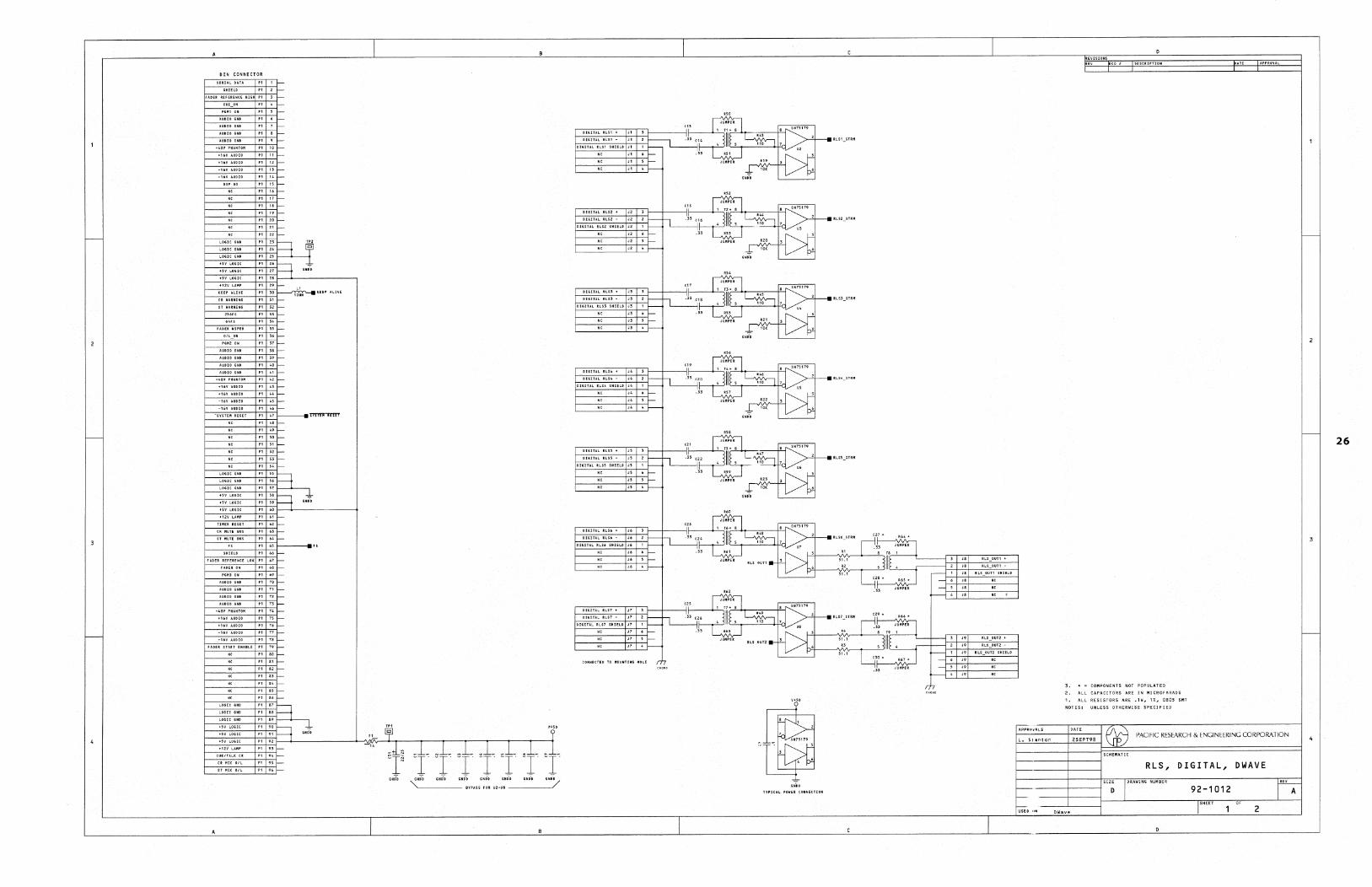
DIN CONNECTOR
PI 1~
PI 2~
.!'AlliER REfERENCE HI&N PI 3 ~
PI 4~
PI 5 t-PI 6 I--PI 7~
PI 8~ PI 9~
+48VPHANTO" PI IO~
PI II I--PI 12~
PI n~
PI 141---PI 15 I--PI 16 f--PI 17~
PI 18,~
PI 191--
PI 20 f--PI 21 I--PI 22~
PI2Sb 24
P1Z0n
"H "
~ + IiNDD
PI 29 j.-t~~iij~=p,~,:g"tF=--.,.;~--. kU' AlHf
PI 31 I-PI 32 f-PI 35 I-PI 14 I-PI 35 I--PI 36~ PI 17 I-PI 38 I-PI 39 I--PI 40 f--PI 41 r--PI 42 I--PI 43 f--PI 44 I--PI 45 f--PI 46 I--
~~~~~-4~'~'ti"~~~ "I-I---~~--~~,~,~,,~I-PI 50 f--PI 51 f--PI sa I--PI 55 f-. PI 510 f-.
+12I1LA"P PI 61 f-. PI 62 I...-
PI 63:--
PI 64~
PI 65
PI 66t-fAllER REfERENCE LOll PI 67 I--
PI 68~
PI 69~ PI 10 J-PI 11f---
PI 72 I--PI 1'3tPI 74f---PI 1'5 I--PI 76/-
PI 1'1'f--,-1611 AliDIO PI 1'8 I--
FADER START ENABLE PI 19 I--
"
PI ao I--PI 81 I--PI 82 I--PI 8l I--
"f-PI as I--
86fPI8.1 n "H
PI 89
I-~.~,v~,~~,~,---f.~~::~~ +$VLo6IC PI 92
+1211 LA"P PI 93 '-
PI 941--
PI 95 f--PI 96 I--
DIGITAL RLS1 +
DIUTALRLS1-
DIGITAL RLSI SHIELD "
DIGITALRLS2 +
IIIGETALRLS4 +
OIGITAl.Rl.$4SHIELD
"
DI6ITALRLSS +
DIUTAl RUS - JS
DIUTAL un SHIELD J5
DIGITAL RLS6 SNJELD '6
DIGITALRLS1'
JllGITALRlS7 SHIELO,7
CONNECTED TO PlDIINTlNGHOl.E
'"
.SB
••
,Hilt TYPlCAL POWER CONNEcn:ON
APP'W"~lS
3. ... = COMPONENTS NOT POPUL.ATED
2. AL.L. CAPACITORS ARE IN MICROFARADS
1. AL.L. RESISTORS ARE .1W, 1X, 0805 SMT
NOTES: UNL.ESS OTHERWISE SPECIFIED
DATE
2SEPT98 PACIFIC RESEARCH & ENGINEERING CORPORATION
L. SUntan
SCHEMATIC
RLS, DIGITAL, DWAVE SIZE DRAWING NUMBER
D 92-1012 SHEET OF
USED ,I" DWave 2
D
26
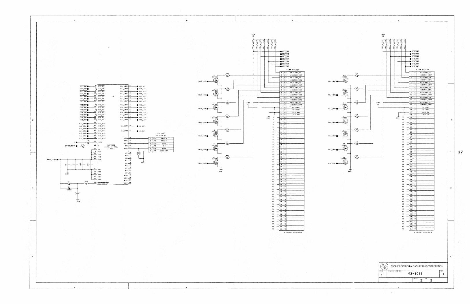
GNDo
= SELl_SII2
SELI_SWS
sEL1_SII~
~ ~ ~
ITCDn ~ 5H2_SII:S
SEL2_SW~
~ ~ sm:::.'fW1
RLSl STR"
RLSZ_STRM
RLS3_STRM
RLS4_STRM
RLS5_STRM
RLS6_STRM
RLS7_STRM
RLS1_HIt"
USZ_S1R"
RLS~ STR"
RLS4_STR"
RLSS_SU"
RLS6_STR"
IILS7 STR"
"t,\JIIU/Ul
DIC.!U! .!~ rPG~
SEL1_LED1
SEL1_LEDZ
SEL1_LEo3
SEL1_LEDIt
SEL1_LED6
SELl_LED7
SELZ_LEol
SELZ_LEDZ
SELZ LEDIt
SELZ_LEOS
SELZ_LED6
SELZ_LED?
SELl_LEDl
SH1_LE02
SEL1_LED3
SH1_LEo4
SEL1_LEDS
SEL1_LED6
SEL'_LED?
SEL2_LED1
SEL2_LED2
SH2_LED3
SEL2_LED4
SEL2_LEDS
SEL2_LED6
SEL2_LED7
GNDO
2N7002 .~
L ZN7002 '~ L
ZN7002 "~ L
2N7002 "~ L
2N7002 "~ L
2N7002 "~ L
~ 2N700Z
-- L -
6Mo-D
V+5o
. . . . - - ~ -f--
. " '50
"' I '"
"' '" 'Lr-· .. '"
" '50
., '"
." '50
. . . - - -
= SELl_SW2
SEU_SW:S
SEU_SW4
~
f-- f----- SELl =SWt> r------ ·SEL I_SWI
SIMM SOCKET
'-- , no SELECTOR1 SW7 , no SELECTOR1 LED7
C-- , no SELECTOR1 SW6 , no SELECTOR1 LE06
5 no SELECTOR1 SWS
6 no SELECTOR1 LEOS , "" SELECTOR1 SW4 , '" SELECTORl LEo4
9 '" SELECTOR1 S>l3
" "" SELECTORl LED3
" "" SELECTOR1 SII2
" "" SELECTOR1 LED2
" "" SELECTOR1 SWl
" "" SELECTOR1 LED1
" "" +SV LOGIC
L- " "" +5V LOGIC
r:== " no LOGIC GND
" '" LOGIC 6NO
" no GNOO
"' - " no
" - " no
" - " no
" - " no
" - " "" " - " "" " - " "" " - " no
" - " no
" - " '" " - " no
" - " "" " - " no
" - " '" " - " '" " - " '" " - " no
" - " no
" - " no
" - " no
" - " no
" - " no
" - " no
" - " no
" - " no
" - " no
" - " '" " - " no
"' - " no
" - " no
" - " no
" - " no
" -52 no
" -53 no
" - " no
" -53 no
" -50 no
" -" no
" -50 no
" -" '" " _00 '" " -" no
" -" no
" -" no
" -" no
?
. . . . . . . ~ ~ - - - - -
sm:svr SEl2_SW2
SEL2.:...S113
SEL2.:..S114
~ - f----- SE l<2=SII()
r-----SEIoZ_SW7
SIMM SOCKET
'---- , m SE~ECT()R'2 SW7 " . "~
2 m SELECTOR2 LED7
2N7002: '" - , "" SELECTOR2 SW6 , m SELECT!)'R2 LEo6
~
L 5 m SELECTOR2 SWS
6 "" SELECTOR2 LEDS
'" , m SELECTGR2 SOIl,
'"~ '" . "" SELECTOR2 LED4 2N7(10Z
9 "" SEL&CTOR2 SII3 - L " m SELECTOR2 LED3
" "" SELEC·TOR2 SW2
" m SELECTOR2 LED2
"" " m SELECTORZ sw1
"Jr '¥" ZII7002 '" " "" SELECT!)'R2 LED1
" m +5V LO~!C - L L- " '" +sv LO~IC
,r:== " '" LOGIC GNP
." " "" LOGIC GND
'~ '" " m 2N7002
" - " '" -- ~ " - " '"
" - " '" " - " '" ""
"~ " - " '" 2N7002 '" " - " '" " - " ""
L " - " '" " - " ""
'" " - " '" "~
t- '" " - " '" 2N7002
" - " '" -- ~ " - " ""
" - " m 27 " - " '" '"
'~ " - " m 2N700Z '" " - " '"
" - " "" L " - " m
" - " "" " - " '" -
GNti'~ " -" '" " - " '" " - " '" " - " '" " - " m
" - " m
" - " m
" - " m
" -" '" " - " m
" -" '" " -52 '" " - 53 '" " -" '" " _55 m
" -50 '" " -" '" " -58 m
" ->9 m
" -00 m
" -" '" " -" '" " -" '" " -" '"
PACIFIC RESEARCH & ENGINEERING CORPORATION
92-1012 A SHEET
2 2
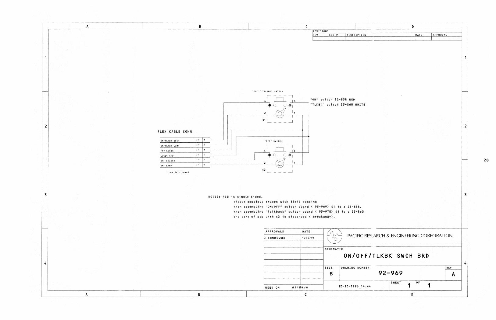
A I B
1
r--
2 FLEX CABLE CONN
ON/TLKBK SWCH Jl 1
ON/TLKBK LAMP Jl 2
+5V LOGIC Jl 3
LOGI C GND Jl 4
- OF F SWITCH Jl 5
OFF LAMP Jl 6
from Main board
3
~
4
A I B
I c I -" _. - --- ----IREVISIONS
IREV IEco # I DESCRIPTION
I I I
"ON" I "TLKBK" SWITCH
I - -- I 41 I I 13 "ON n switch 25-858 RED
1 0 1 "TLKBK" switch 25-860 WHITE
21 II
11 1 ~ 1
S1 L ___ ~
"OFF" SWITCH
- --I I 41 CJ 13
-' 1 1
21 ffif r 1 I ~ I
S2 L - -- ~
NOTES: PCB is single sided.
Widest possible traces with 12mil spacing
When assenbling "ON/OFF" switch board ( 95-969) S1 is a 25-858.
When assembling "Talkback" switch board ( 95-970) S1 is a 25-860
and part of pcb with S2 is discarded ( breakaway).
,--- ---APPROVALS DATE
D -
IDATE I APPROVAL
I I
J DOMBROWSKI 1215/96 ~ PACIFIC RES lARCH & ENGINEERING CORPORATION
SCHEMATIC 1------
ON/OFF/TLKBK SWCH BRD
SIZE DRAWING NUMBER REV
- B 92-969 A
I SHEET 1 OF
1 USED ON AirWave 12-13-1996 14:44 -
I c I D -
1
r--
2
r-- 28
3
4
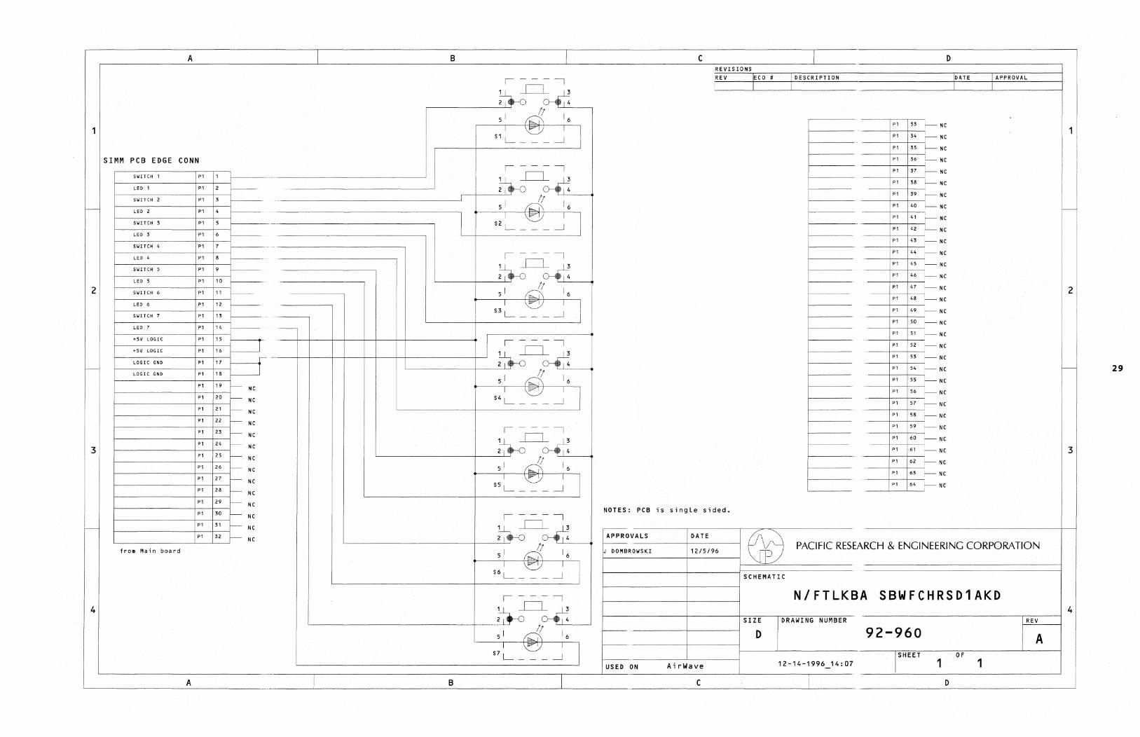
1
--
2
3
4
A I B
I V S1 L __ _
SIMM PCB EDGE CONN
r-__ SW_I_T_CH_1 ___ -+_P1_+-1_J--------------------------l
r-__ LE_D_1 ____ -+_P1_+-2_~------SWITCH 2 P1
1----......... -------------------
1------+---+---1 l SWITCH 3 P1 5
LED 2 P1
S2~ _'?_ LED 3 P1 6
SWITCH 4 P1 7 f-----.-... -------------~ f---------+---l---
LED 4 P1 8 1-----_.
SWITCH 5 P1 9
LED 5 P1 10
SWITCH 6 P1 11
1 V 53 L __ _
12 LED 6 P1
SWITCH 7 P1 13 1----...... ---_
LED 7 P1 14
+5V LOGIC P1 15 1---_..- I +5V LOGIC P1 16 1------'1 1
1----LO-G-I-C-G-N-D---+-P1-~1-7--\ 1--·---r-t--+--r--+-1--~~------~~ 1 T 21
18 1 LOGIC GND P1
I
~
1
~
I
3
P1 19 r-- NC r---------+--+-~
P1 20 r-- NC 1---------+-+-__\ 1 V I
S4 L ___ ~ P1 21 __
I--_______ -+_~~ NC
P1 22 -- NC
P1 23 -- NC 1---------+-+-__\
24 ~ NC 1---------+-+-__\
P1
P1 25 NC
P1
P1
P1
P'
P' P1 31 __
I--_______ -+_~~ NC P1 32 __
L-_______ -L_-+_~ NC
from Main board
I ~ S5 L __ _
1 V S6 L __ _
1 1 -0-L-__________________________ ~--~ ij
51 d I V
S7 L __ _
I
~
I
~
3
'1 4
1
~
l
l
I
l
I
l
c ,REVISIONS
:REV IECO #
! T
NOTES: PCB is single sided.
I I DESCRIPTION
T
P1 33 ~. - NC ---+-+--
P1 34 -. - NC ---+-+-----i 35 -: - NC ---+-+---: 36 -: - NC
----I----l---'
P1
P1
__ --I_P_1 -1-_37----.;-, - N C
P1 38 f-- NC ----I---+------"
1--_______ --I-P_1 -I-_39----i1 N C
P1 40 ~. - NC ----I----l--_
1--_______ --I-_P_1 --l-4_1--\INC
P1 42 t-- NC ----\---1---
P1 43 '~! - NC
P1 44 f-- NC ---+---+--
_ .. __ -+P_1--\_4_5 _r-- NC
P1 46 ~: - NC ---+---+--
47 '-. - NC ---\--1----" 48 1-- NC
----I---+---:
P1
P1
P1 49 '-: - NC ---+----I-~
.. __ -I-P_1-1-_50--,'-, - NC
___ -I-P_1-1-_51--i~NC
___ -+P_1--1_5_2 _i-' - NC
P1 53 I NC ---+---+--
54 r-- NC ---+--+---!
55 _~ - NC
P1
P1 ---I----l---I
56 ~NC ---I--+-----.;
P1
P1 57 ~ NC . ____ 1----1-_-' P1 58 '-; - NC
__ -+-P_1 -+_59---i'~' - NC
P1 60 '_: - NC
----i-P-1-+-61--:~1 - NC
----I-----l--....;
___ _+_P-'--I-6-2 --,'-; - NC
__ --\,...P_'--I-_6_3 --,'-, - N C
P' 64 -' - NC . __ -L_-'---i
D
IDATE I APPROVAL
I I
~-----,-----,--?-~--------
APPROVALS DATE ~ f----- .------1-----1 J DOMBROWSKI 12/5/96 D PACIFIC RESEARCH & ENGINEERING CORPORATION
SCHEMATIC
N/FTLKBA SBWFCHRSD1AKD
SIZE DRAWING NUMBER REV
~ --------+----~ 92-960 o A ---------------~----~
ISHEET -----~------------------------~
OF 1 1 12-14-1996 14:07 AirWave USED ON
1
--
2
3
4
A I B I L-____________ ~ _________________ L' __________________ ~ ______________ ~ _________________ ~C ______________ ~I ___________________ ~O ________________ ~
29
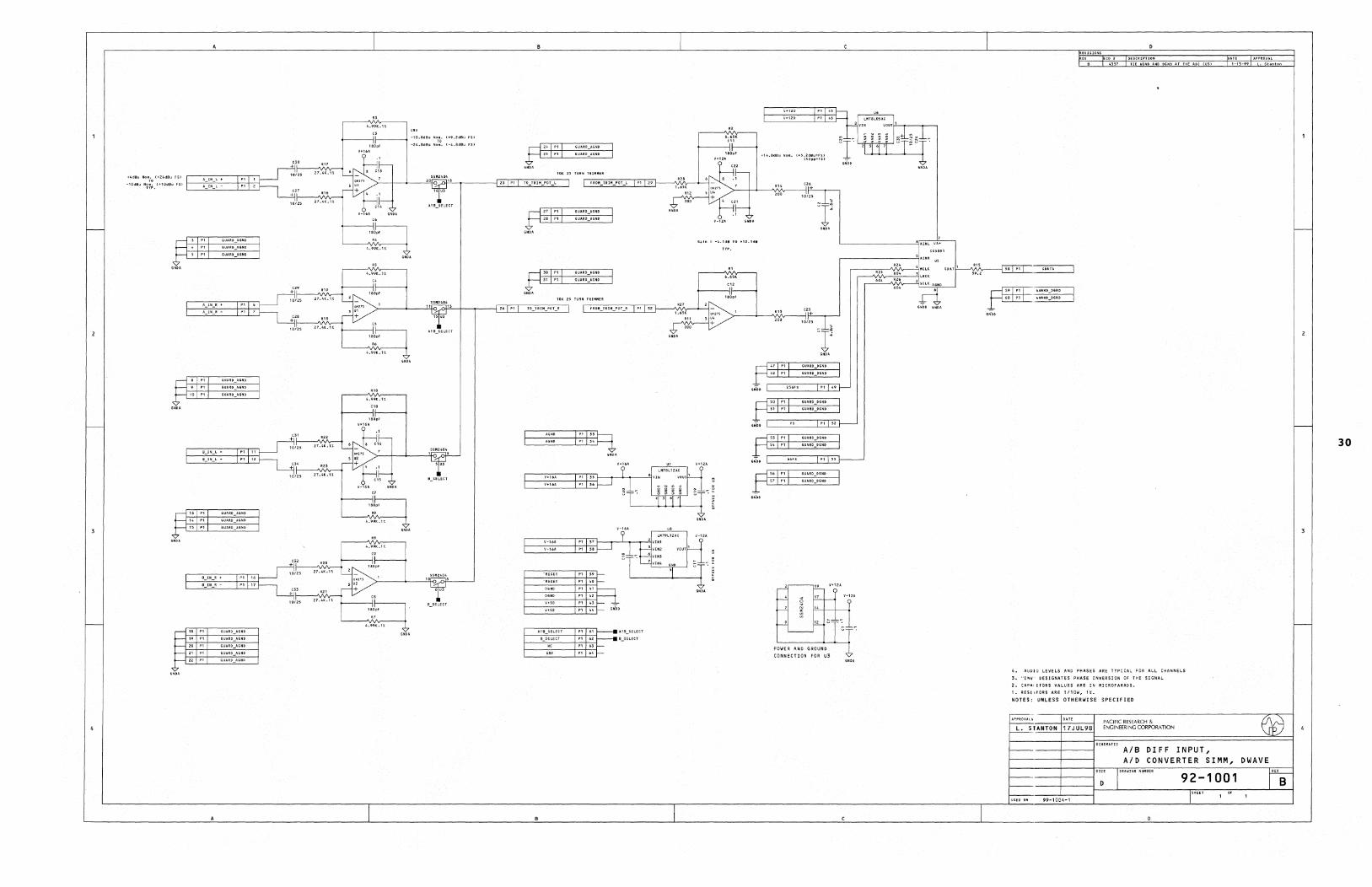
I
i1 -IO.adeu It()T~' (+9.2dBu FSI
ISIJpF -Z4.8dBuNOII. (-4.8dBuf$)
~ -t131f!
6 8 c1,1;--101/25
.+,40::" N:o·!? \+:,40d::u fFS:) ;;275 7 ~O~4, A_llt_L + 20 18
TYP. "_I"_L - 5.+ 4 .1 .I. ..tIlt 1fNz~
t'14 A!B_SELECT
V-I6A GNDA
\1 18IJ~f
liUAROAGND
±. i:
m
~/25 tS1JPF
~ A lit II + OP27S 11 13 A_IN R - ,0>
.~" '" + +
~h A!B_SELECT
&~ 6UARD flGND
GlIARD_AiND
GUARO_ASMO
~t--
~ '" +
6 8 CHi
B_IN_L + ;;215 7 ~ , , B_IM_L - , " .r. C34 +
+ ' ., m B_SELECT
V-16A liNOA
GUARD_ASHD
r-jb .. &UARD_AGND Gt QUARD_ASHD
~I'c Is1JpF
1.0i/ZS
O~l B IN_R + OP2?S .. 8 B_IIt_1I. -
,,, .r. .tr't +
101/25 ;: IS1Jpf B_SfH .. ECT
4.99t1,.U ,i r-- GUAU_Alin
I- GUAU_A6ND
I- GUARD AGND
f- GUARD_AGNO
f- " " GUARD_MiND
I
GUARD_A6NP
27 P1
I
IOP275 sjU4
,ir"--'V,v,,v-----l + ,
IOP275 sjU4
r-'I/\/\~~+ -L 200
6~
r==:;;~=~:;:gQ---r'J·?'-·"r--1 LM7::,2AC ,,[V+~/A L __ --'='-__ -'-".:.'.L.::;:'-'~ ONl+-. 8 HI VOUl
'
_. n n ~*" '---__ ' ...... J'J ....... \-+-'J -----1
V~6A I LM79L12AC
'-__ ....:...= ____ L:.:.:.L:.:::.J~ ~l. r! :::: ""I-
~T-:C!:::: 'lND ~::=-: P1 39 f-- l_ ~RESET
I
IW. __ !i .
-, It.IdSu No •• (+~.2dBu=FS) (4Vpp=fSl
, 8 AINL VU
,-______________ ----'15 AlNR
m ~ ____ ~-J~~ __ ~+
PI 49 t--
GriDD
57 Pl
-..1-fll- V+1Z11.
-! 0 flLf----1 ~
PO"'ER AND GROUND
CONHECTION FOR U3 6NDII.
ZSCLIi:. AGND ,n
I
I
4. AVOIO LEVELS AND PHASES ARE TYPICAl. FOR Al.L CHAltINELS
3. "JHV" DESIGNATES PHASE INVERSION OF THE SIGNAL
2. CAPA, ITORS VALUES ARE IN ~ICROFARADS.
1. RESllIORS ARE 1/1QW, u. NOTES: UNLESS OTHERWISE SPECIFIED
~;-----'-------r--------------------------------------~QpJ--~-1 PACIFIC RESEARCH &
~'AHTON 17JUL98 ENGINEERING CORPORATION
f----+-----l
~.---+---~
~
99-1004-1
D
AlB DIFF INPUT, AID CONVERTER SIMM, DWAVE
'''''''' ,,"EO
92-1001
-
2.
-
30
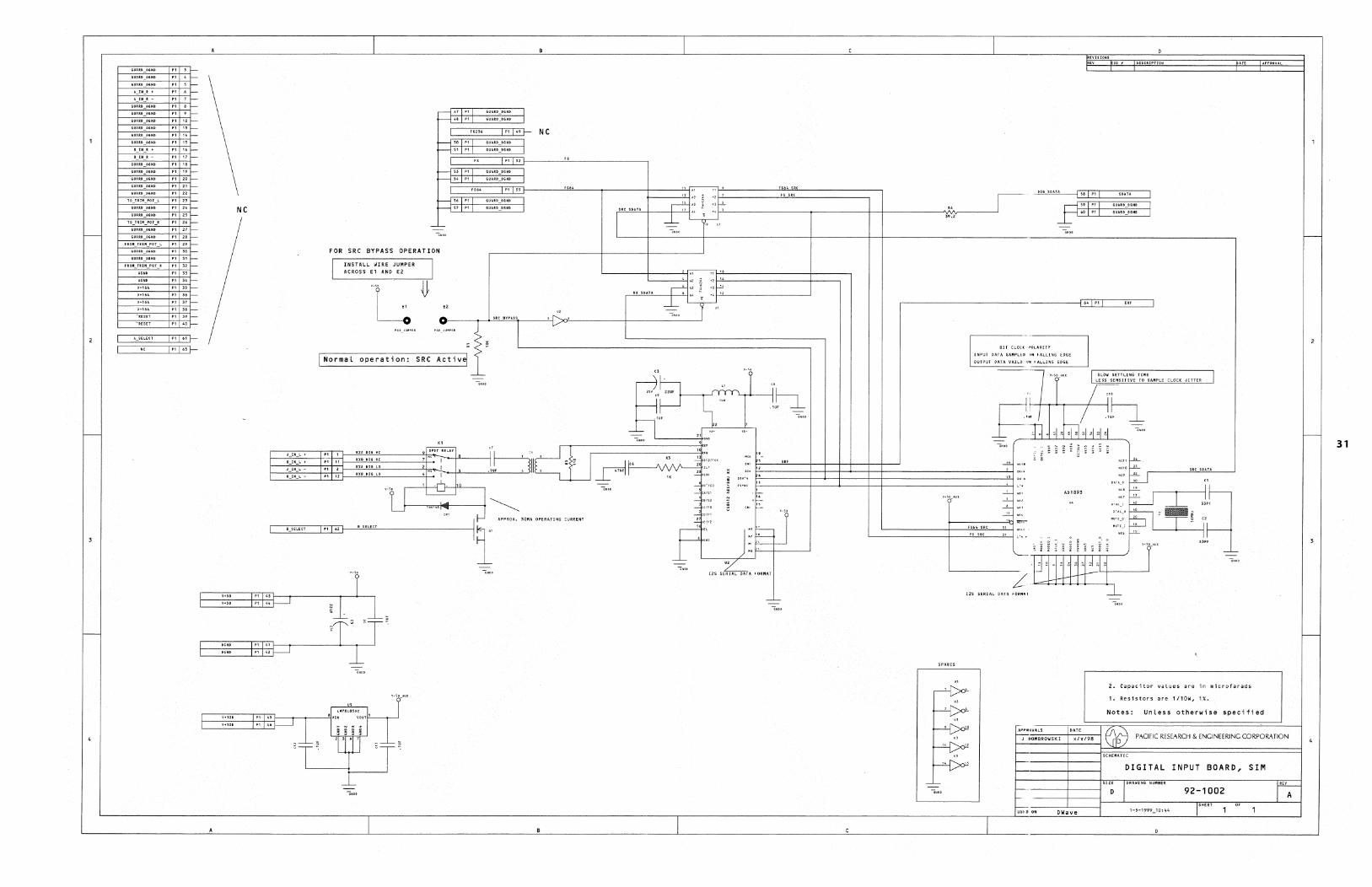
---
IiUAU UNit
GUARD_AliNI>
fiUARDAG"!>
Alltl.
AINIT -
GUARDAGND
GIIAID' AGND
GUARII AGMD
GUARD AGND
GUARD AGND
IiUARDAGND
BINR+
I_IN_I -
GUARD AGNI>
GUARII_"6ND
liIlAtD_"GND
liVARIl A6N1>
GUARD "&Nil
TOTRIII"UL
GUARD A&N1l
GUARDAGND
TOTRIIIPOTR
GHAltAGNt
GUARD A&N1t
FllO"TRIIIPOTl
IiIlARD_ACNO
GUARD AGMO
FIb" TRIPI POT_I
V+16A
V+16A
V-16A
V-16A
-RESET
-RESET
P13-
Plio -
PI 5-
PI 6-
PI 7-
PI 8_
PI 9_
PIIO_
PI 13-
P114-
PI 15_
PI16-
PI17-
PI18_
P! 19_
P120_
P! 21_
P! 22-
PI 23-
P124_
PI 25_
PI 26_
P127_
PI Z8-
PI 29-
P1 30_
P131-
PI 32-
PI 33:""
P1 34 f--PI3S_
PI 36~
PI 37~
PI 38~
PI 39 I-PI 40 f--
I" I" f_ I" I" f_
DUD
ono
V""~D
V+t2D
NC
I 1 I EVISIONS
r--i 47 PI GUARD ItGNI>
t------l 48 PI GUARD bUD
1 "'56 1 " 1 "f_ N C t----i 50 PI GUARD "61tD
t---i 51 PI
t---l53 PI liUARO_D6IU>
t---l 54 PI 6UARD_DUD
t---lS6 PI GUARD DUO
t---l 57 PI GUARD DGND
11 ~~' ____________ L"~'~'~SR~' __________________ -,
+--------""'-1 A~ <21-'-' ____________ --""'-'-'S'-''''---______________ -,
~S~"~"~AT~A-+----~~f_-""~U ~ y3~~L:------------------~-------------+--+_------------~RV.~------~ I
~"~~"' ".2 GNDD
60 PI liUARD OGHD
f$64 • __ DIG SDAY'" 1"1"1
59 PI SUAU OGNO
FOR SRC BYPASS OPERATION
I INSTALL WIRE JUMPER ACROSS E1 AND E2
'L I
E2
-
"
L-________ ~-------'y~~"~------------------+_------_. L ______ .;..,' A2 :: T2 ~"L...------------------+_----....,
RXSDATA r. A3 ~ Y3~ ~~--JL~~ .... ~.~,,~"L--------------~
~!:-.~"" ,: "-Ih H- . to, , ...
_ ~ '" "~...!,,.:02------.L •. -,
GNU GNO
I an C L.Oll: '~QL.ARI TY
INPUT DATA SAI'IPL.lLJ IN HL.LING EDGE
OUTPUT DATA VAIL.LJ "lit tAL.LING EDGE
,,'or
1"1"1
1,..--------------, I SL.OW SETTL.ING TIME j
L.ESS SENSITIVE TO SAMPL.E CL.OCK J.ITTER
'" F-'-' ____ .... '''''' ____ + __ +_-1--+_---1-_+--"
r::::=~A?"~' :::·=+-'~'-l.0'+.,~--_;"~·~·:;;"~"~'--------_;7~~~:CP~.:..T 1;·~~"~y~----~inlL-----..c...,il~ , " ~~~~~~:~::~f~~:~~~f:~-i:±1"l'2~'Ej::~:j:~::t'~':====J2$:-l~iL------.l~~:,,-------':J~il : :~~ I .--.J1C6 A ;'A A ~ :::"" = t BIll L - PI I~ IXS DIG LD 4 I' U --L ·", .. 1 r--- v ~ v ~ ERr m"A ~,!.: ----------+--~_I------+_-+-----------------------------':'13 U'~ -;- :::: NCIO ~ ~--------.!!SR;S'..!S!!"c!!TA~---, mt:!=J
I~' V_50 1,--21+-"'1 r-lhl.lL..O __ 1 GNU -.: :;:~o noNe ~,'-----------I------..... -----+---I----------------------------'-1 ,.,
l...--- - -c 'b V.50 AIJX .....l- Nt'
............... .....: efn "I;;- .....L "'I AD1893
" ,
~ i ~ '" " !Ii! a. '" z !i! '"
[I=~'~SE~'~EC~T=J::I ,~']I~.~2}_1--...!'!.J'l!.'!,.!"l!CT'-----~~~~~~-'~ .. T1"'· .. -,.j-.. ~'-··'~~~~~-'-l~"" ,,~, .. ", .. ,," '""''' ~? ! J -:~ L-__ L __ -_-_-_-_-_-_-_-_-_-_-_-_-_-_·~-=-~::-=-~~'-,~',-.~.-,~:-:~-,::-=-~::-....2.:::;::-':~:~'~ ±-- ~. "'/ , __ /. 01 '1·1 ,I "1·1 "I d ·1-II
NC8~
~,!" XTAL0
40 -- .. ", .• ,~.""""i""";C2
"UTEl~1 I I
Ne7 I-ll- I I--;!...-l
N~6 i--!-L I 33PF
,... I2S s~. '''.AT - £.-_ J-.+-+-t-t-r' 12SSERIALOATAFORMAI ~
G~~~
SPARES
2~ Capacitor values are in microfarads
1. Resistors are 1/10W, 1% ..
Notes: Unless othe~wise specified
---
f---
r .. ~---~~~~================~~ A .... .,IJVALS DATE O\~
1--,-,,-o'"'o""o-.o"'W""'-'''"1 -I--x-:'-x""'9:":8:-l \Jj"~ PACifiC RESEARCH & ENGINEERING CORPORATION
SCHEMATIC
DIGITAL INPUT BOARD, SIM
-- ~ _________ -I-____ -ISIZ~ 1,",wI •• NU ....
92-1002
~·-O'----~D~w~.-v-e----~ OF
1 1 1
31
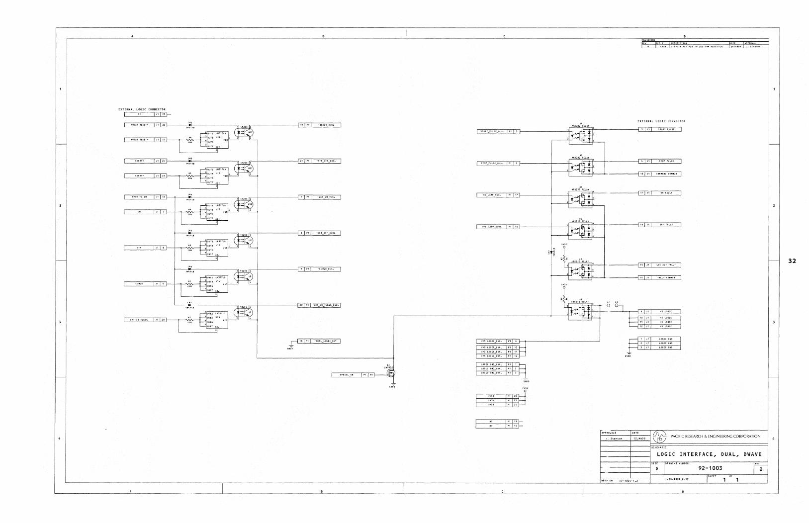
EXTERNAL LOGIC CONNECTOR
IJl123~
r18!~11
GNDD
" lN70(t2
REVISIONS REV CO ,~
EXTERNAL LOGIC CONNECTOR
51 J11
Ii 1:5 I J1 I C(t" ...... N~ C(tM"'ON
1"1"1
1101 J11
II lSi J11 32
1141J11
13JAN99 PACIFIC RESEARCH & ENGINEERING CORPORATION
LOGIC INTERFACE, DUAL, DWAVE ORA~ING NUMBER
o 92-1003 B SHEET OF
uSt (> ON 99-1004-1,2
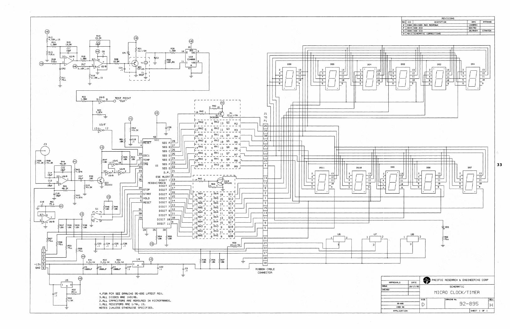
AEUISIONS
FEU ECa DESCRIPTION DATE APPROVED
E 3:303 REUISED ~O AEDAA,",H I 3MARS I F 35i'l SEE ECO 50CT92
+8 G 3683 SEE ECO 28JAHSi STANTON
RI2 i.32K,.I~
Ali AI5 1.96K 19.6K
CR2
AI7
3.16K,.1r.
RI9 19.6K
CI2 10pF
"
+8 C8
j~ 6 8
~ AI8
+8
r-
A21 A26 In. II2W 1.96K
CAL
·~~~.i~ } A20 A50 15.8K 10M,Si::
C21 I Q21 '_1 I -
.1 I TlPI2~l -b CI I
H 1013 SCHEMRTlC COAAECTIONS
+8
16
10 UDD S if OSC
UI0 CDi060 r I AUSS 8
12
f)S6 DS5 DS1 DS3 l)S2 DSI
2 13 ~ ~ ~ JE ~ 13 2 .
13 2 13 3- f---t2 3 12 ~ ~ + f--t2 fJ ft2 IJ f--t2
t-:;- I---tT f-:t r--u- t-- ~ f--o-ALL 75n.
2.10K,.1i:: I -:- 68PFli
-:-L ___ ':::...J
I-I is- t , fte
I-I '-I r----u- L-!... L-~ t , f-Te--I I ~
I-I '-I I-I '11 LL ~ 5 t , f--t0- I I 5 I , ~ ~ 5 10
A23 7.87K
U3/F
~
+5
RSI 10K
+5
A52 i3.2K
A2S A2"1 b OSC 1 37
: - - - - 2-A~2 ~5 50 ----: I 16 RN2 I ~ Al I I Q~ 22nl/2W I
2N3638A TO
+5 JI
'L-
-
6 f-S 6 l-
f- - - - - - - - - - - - - - -1 PI ----, .-___ I'1 RN2 3 'I RN2 13 Q2 R2 .--tf0 ~2~~ ~ = ~ ~~ ~ 1= ~3= = R~ ~ L~H+H+l-+-H-t--++!f-J----------'
-f6~~ ~ _ J ~~ ~5_ ~~ _R~ -1~ L~H+H+l-+-H-t--+..!----------, SEG A~ '----9 RN2 8 7 RN2 10 Q5 R5 ~ ~ 3'11-4-+-+-t+-HH-t+---t-.
f---------------1 I--SEG 8 ~ r---I'I RNI 3 'I RN I 13 Q6 A6 ,.:: 1-----+-t++H-t+-+h
SEG C ~ ~ - - - - - - - - - - - - - -1 331---+-'-+-1-1-1-1-1---+++-.. SEG D~ r-12 RNI 5 6 RNI II Q7 R7 I--
~ - - - - - - - - - - - - - -1 321-------+++++-1--,
f-s f---s rs- r-- rs-I- ~ I-S f.--..:- f- ~ I-'
+U SEG E 2'1 -10RNI 7 8 RNI 9 Q8 R8 ~I-----+-I-+++-h SEG F 23 ~ - - - - - - - - - - - - - -1 I-- 'tltrt=====++=I+t=h=====+t~=====++tI=t:;=l=====~t:t++,
UI S~~P~ ~~ ~~:~:~ ~ ~ ~ == ~5~ ~9 ___ ~A~...J 1--1-'1 - I
Ai7 U3/E 10K 10K ~ TCMP
~eKL1'" 10 ~IRQ A~2 U3/A ~ 7.87K 3... 1 I... 2 ~
ESE ALERT ~8,---___ -,1, CI7 A16 ___ U3/B 2 ~~-+_10~ul~F~~1~0Kv_~(~'~ VV 3~ DIGIT I 19 I Ii RH3 3 ~~)QI0 I ~
A~3 i.87K
AiS i3.2K
Q23 2H2222
+5
MC68HC705C8 18 I AH3 MPSUiS 1 121----11---' DIGIT 2 ~ 3 i I ts
.---__ -=-3'1-'-lSTOP DIGIT 3 17 -b f--+---' .---...:7~START DIGIT 'I 16 ,I f- ;AN'I-8 - -7 RNi ~:- -QII-1 ~t--+-----' ~ __ 6"4HOLD DIGIT 5 15 ILJ-I ;RN5-1 - -; RNS ~5- -QI2-1 "If--+----' ~ RESET DIGIT 6 1'1 f-1~RN5~ - -'I RNS ~3- -QI3-1 '31------I-----==r--r--------t--------"f--...J
1>58
1-1-* D.~
r---s f--
DS7
I-I t ,
I-S f-
SI A~8 10K
A~S 10K
DIGIT 7 13 f- - - - - - - - - - - - -1 I--12 12 RN5 56 RN5 II QI'I 151--1;---------t-------+---------t---------11-----------+----~-____ -...1
DIGIT 8~f- - - - - - - - - - - - -l I l-
# 1
AS? 7Sn
A27 10K
AS8 7Sn
R28 10K
ASS 75n
+5
A29 10K
AG0 75n
A30 10K
+u R31 A32 A53
II 12RN'I 5 6 RN'I II QI5 131--1---------t-------+---------t---------11-----------
DIGIT9~ ~~~~-~~~~J IF~I-~========t=====~========t========~--------~ DIGIT 10 ~ f- - - - - - - - - - - - -1 1-9 j DIGIT 1! ~ f-1§.R~'1_I __ 2 !N~ 1.5 __ Q":7 -1 I, 1-_____ '--___ +-_____ -+ ________ -'
L--"T---'---......--J L-_-"; 10 RN3 7 8 RN3 9 QI8 I-- CA3 20-:-' 35 38 f- - - - - - - - - - - - -1 I~ * .J.- L-_-...;f-I~R~35_ 3!N! 1.1 __ Q":9 .------'
A51 ASS 10 RN5 7 8 RN5 9 Q20 1-31 rc?-U6 rr-U7 2 rTU8
2 10K 10K L - - - - - - - - - - ~2~~l2wJ I ~I--------------' 1 I 3 2 3 3 ~~
~ --:- ~~k S21-------------------------~ ~ Lt=E==============================~==~==~===i========~======j~ L-~ ______ +-_~ __ ---'
r-------~~r-------------------------~r_----------~--~-----------L-----+----------~ U'I A3S A36 A37
~I--f3"1---------J ~I--------------' 2.2n1W 2.2A IW 2.2n IW ~ +13U~I-~--------------~I-~N-~--~~~~~--~_4
GND~1 Y--------------'------'------'------'----4--------J
f?3 'T 1C22
I-.-__ ~181---------------------------~---------------L-------------------' I RIBBO';CA8LE
-:!:-10K 10K 10K
lc9 l
U5 +8
'-rQ-C7 • 1
A33 26ln
A31 1.5K
!tI~0uF Ci C27 100E1uF 1000uF .1 .1
~
'1.FOR PCA SEE DRAWING 95-895 LATEST REU • 3.ALL DIODES ARE IN91'1B. 2.ALL CAPACITORS ARE MEASURED IN MICROFARADS. I.ALL RESISTORS ARE 1/4W, 1%. NOTES ,UNLESS OTHERWISE SPECIFIED.
1'1 CONNECTOR
APPAOURLS DATE ~ PACIFIC RESEARCH & ENGINEERING CORP
10/17/S5 SCHEMATIC CHECKED
MICRO CLOCK/TIMER
~ ___ -=$~~~ ____ ~s~1 USED ON
ORAUIN6 No.
92-895 APPLICATiON SHEET I OF I
REU
H
33
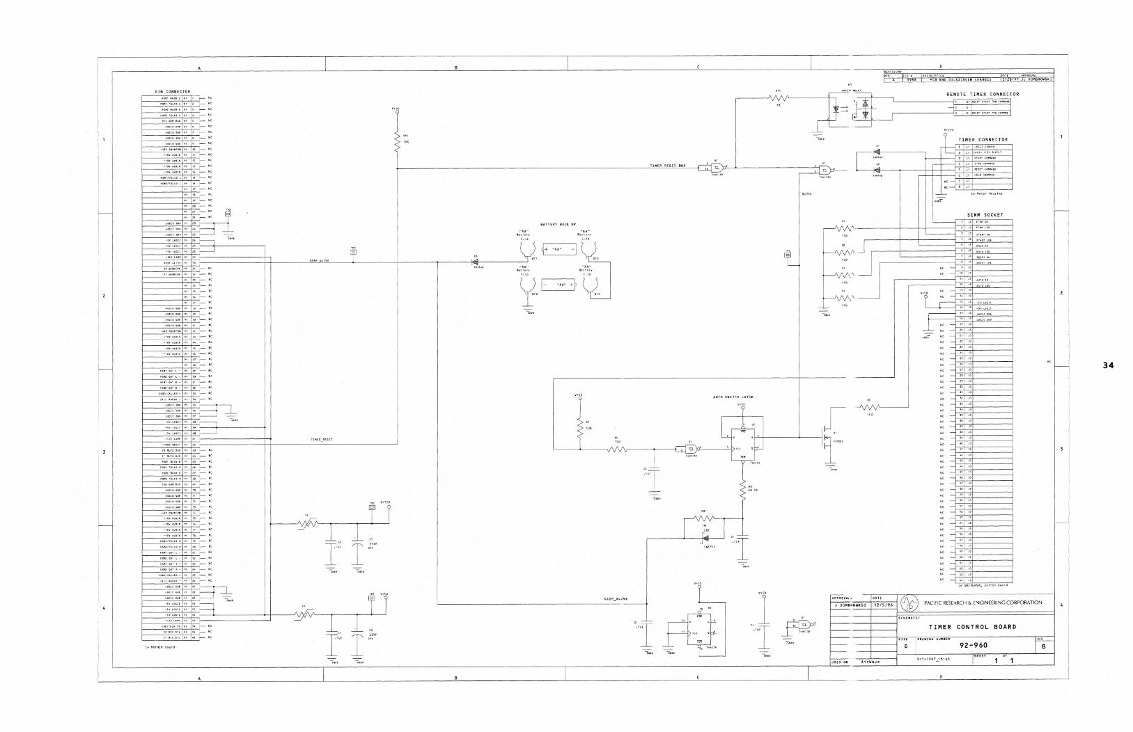
DIN CONNECTOR
14 f-- NC
PI 19 _Ne
I---------:::~:: ::::: :: §-!
PI H '-- NC
40 _Ne
PI 4$ _NC
PI ,0 _NC
~~~~~:~ PI ,4 L.......- Ne
::----r ~I 2V L~MP PI 61
66 ;-- Nt
r-__ ~~'-4~i"n~;-- Nt
f------'-=='-'-\"--f'-"'-- Ne
PI 56 ~NC
,,,,,'"",,::=r-=::r------';;~ ~ :;S ,0",
·'VLOGHPI ?I~~ __
-,V LOGE PI n
1 1 I
l· .. 150
TIMER RESET BUS
L---~----~/\/~\/\c----~--~
,,-.IUF'
" II b'-~-----------'--r=-, ,ll
n )::j------'-I)
" 68.1K
I
ECOd DESCRIPTION DATE ,APPROVAL
3988 PCB AND S!LKSCREEN CHANGES, 2128197, J.
REMOTE TIMER CONNECTOR
TIMER CONNECTOR
N(- 8 JI
-- '0 Me:er ~ou.i ng
GODn
SIMM SOCKET
Ne _ 19 J3
Ne - 20' J3
Nt _ 21 J3
Nt _ n J3
lie _ H J3
NC - ~.\ J3
Ne _ 15,' 13
~C - 26 JJ
Ne - Hi J~
NC - 25' H
Ne - ~9: J3
Me =f--~--~ ~c _ 32 J~
NC - B H
:~ =~"c-c,c1, -------1 Ne - 36 J3
NC - '7 H
NC - 38 J3
Ne =-~::r----------------'"-Ne _ 41 J3
Ne - 42 J3
Ne - 43; J3
:~ = i-c"c-,c-, 1--------1 NC - 46 H
Ne _ 47 H
Ne - 4B H
NC - .9 J3
:~ =1-0,,",-,"'-,1--------NC - 52-: J3
~C - 53 i n
NC - 54 n
NC - 5,: H Ne - ----=6J J3
:~ =1-",,"-,e: --c+----NC _ ,9: J3
NC - 60! J3
- " " _ ~2! J3
Ne _ 6~ J3
Ne - 6"1 H
'0 UN I ve R SAL • w ; ~ c h boa r d
TIMER CONTROL BOARD
-
34
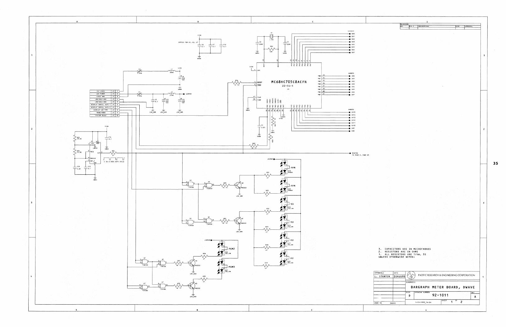
I---
-
4
+SVLoIliIC
LEDPOYEF!:
DISPLAY vurp,,, ·P&H21PSI'I3
·SVSTE" REliET
!!~" li 1.'.', ,-----'-1' :" 'm I .,.. DISC"' i , " 1..11555 ,;;;;,
H 1 I--
J19~
Jl 10
1 I 27UH
C3 Jj-", ,., l~l:
LED~G"D LED":"GND
11+50
"'''' ... """', "1,, I" 1m r'" T'" T'" 6Nb"O
-rLEPPUR
J±C1' 16V 1m
I
v+r' . L...!... vpp
,-------------------11 '" ,-----------------.... '" ..------------'--------11 '" ,.------------------11 '" ,.--------------- '" ,-------------- '" ,-------------. '" ,.------------.... '"
- - ~ .. , .. 1
............. ~ ...
ANODES
'" " AD, ", ,. AD,
, MC68HC705C8ACFN '" " '" Tm1' 16 , '" ... 1m" 22-54-1 "
." ~fL----2q
'" RO' " '" " ...
'" " ... '" " '"
r~~:;:
_ ... ~~::E ... ~~~~~E~~ .," '-------T--~ ~T-ii-'i~. ~I'-T-T-~I ~I ~~I •• -T-T--' •• ~r-:;....:r~ ~ -T--~I,------' ____ .... ::"
I.J. '-------------• .\1114 1. =~ V.S~;;D '-------------- AD'3 _ '-------_______ ---11 A012 '-______________ --11 ADt1
C4 ~ '-_______________ -11 ADto r'·., -. '-______________ -11 ... - '---_______________ -11 ... GNDD
~--------------------~~f'
I
< 14.31( OUT~ Y...yt----t-+,--------------.,..--------------------L-----------______________________ I'lINTE" "" r. u,. , A .". I 27 TO PUE 2. lOME D3
+------+-':'-I;:~H~D .r-u-u-u ~'!!-- 2 KHz a 80X IIUrY CYCLE
" " , ~4
, , , 74H(02
" " " " -;q ,.
" 74HCD2 74HC02
I
'" u: 1%
R38
11i: 1%
"' ~l'.-..... --'<::r-u-''\,.
t3D 74HC02
' .. 1 P82222
' .. , PM2222
1/:: IX
LEOPWR .... --,----,
A.~···i If ,! i ,: PGM2
136 A 1 ... 1..1 ~~fL.OW
4,f~----~~lf~r----:----J ," : , . PGM3 ! ,
~. 1J~:~LOIt ... 1'------'
LUPIIR ___ --....... ----~
, , m~ ';, PPM
If j:::u ,.--------,--J\" !'--=~r---~ J " '" If , . PPM ,'''2222 I 21
123 If J :::EN
"f'-----"mlf~~ -,l -,--J : : VU .L ,
If. 1015
..-___ -. ___ ,A\ "'/,-__ ",'-;_1 '_'_"_" __ ~
"m 1 ,I i ,. vu
If. I ~~~LOII ~!'--~r--~
1~: ! ! 2; VU
~fL--~~~~!-:E-'[-"-W--mlf ,I, i : VU If. 1 DZD
I--------.A R~91'_ ! __ ...!!= j YELLOW
-v,.,V
'" ,'N2222
I I
3. CAPACITORS ARE IN MICROFARADS 2. RESISTORS ARE IN OHMS I. ALL RESISTORS ARE 1/4W, 5% UNLESS OTHERWISE NOTED:
;A~:UG98 €JE3 PACIFIC RESEARCH & ENGINEERING CORPORATION APPROVALS
L. STANTON
SCHEMATIC
~-----~-~ BARGRAPH METER BOARD, DWAVE
SIZE ,ORAWING NU'.ER r;-f..--. D 92-1011 I--
~.)It ISHEET 1 OF
2 DWAVE ,·1 S·' 999_16:34
-0
f--
3S
I---
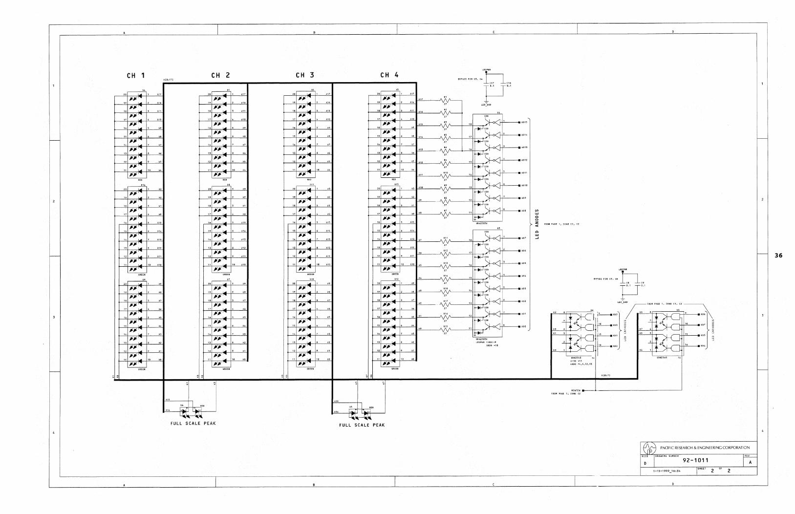
CH 1 CH 2 CH 3 H0=171
20~' JlJI'"
19 ~ 2: 19 JIJI , .....
.17 20 .... .,
JlJI""-19 2
18 JlJI... , '" AI.
17 JIJI ,..... , .10
16 JlJI... , JlJI .... 16 ' .... 5
JlJI'" " 6
" JIJI , ... " , " JlJI..... , " " JlJI... ,
JlJI .... 12 ... 9
11 JlJI..... 10
." 20 ... 1
19 19 JlJI,..... 2 19
18 JlJI... ,
17 JlJI..... 4 .. 17 JlJI,..... , " JlJI ....
16 ..... :5 AI, 16 JlJI... , 16 AI'
" '14 " JIJI ... 14 ..... 7 14 JlJI... 7
"JlJI,... , " JIJI ...
12 ...... " AI' " JlJI... , JlJI .... " ,
AI, 11 JIJI ~ 10 AI.
JIJI ...
20 .... 1
19 JlJI... 2 JIJI ""
19 2
JlJI .... JlJI'" 18 ..... 3
JIJI ... 17 ,
16 JIJI = , 16 JlJI,..... ,
"JlJI,... , " JIJI ~ 6
JlJI" 14 7
JlJI'''' " JlJI..... 7 " JlJI .... 13 .... 8 " JIJI ~ , A2 " JlJI''''
12 JIJI = , AI
JlJI .... 11 .... 10 11 JlJI,... 10 10 "
I-'-A"'''_---;[.'1~~ .. ~··l-'w--k-4U L~~.-.-~~
FULL SCALE PEAK
CH 4
ZO~'
BV"""'",,",LE~ ~C17 J.-C16
p'" '( I /11+'------11'
u "'II ~ 5 A9 AtS «31'_--j---!'!-'f--t"~; AtlS ~~~~~~~~~--~~~7 ~~, ~2 t---""h.,.;-i'Irr'----""-'-J...!'!!14'----..!\ as 1'----f--"!...7H_-t"~, f-\-!----<I -.DU.
14:,," 7 A7 '" :: A 16 f-*J~f+!' ____ AD13
" J'J'.....,.. 27 f-*J~, ~, t--"'''t-;;;-;;;-I''" .. f'---''''-'-J...!,.!J''L----..!\ "1'-___ _"'1' H_-.... ~, 1-f.'---.U1i!:
11 JlJI 10 A4 27 ~Y~I ......., 5
+--"+-;~"~Ji .. -I-'''----'''-I~A1!!' ___ .../\''.I'_----',;;,I+_-t"~; 1-12----<1 ""
f-*-i'(, ~, 1--2!!.+-::7::,-i"" .. ·I--"-.J..!'--.-!,~,_t""'IO'-----'\ "; A'-___ -"=_, H_-t"~' "-12----<1 ADtl]
J'J' ' 27 f-*-i '(, ~ 7
r-!!19h~~~~, ........ 'Ir2----'·"-'L,~,----- 1181'-___ -','12 H_-.... ~, f-f!---.'" 11 1...if..:5 A1 27 ~Y~I ./1s
1-_~17+_:~~~~<1111_~4--.-!'~O~,!-,---~.71'-----',!...,H--.... ~, 1-12----<1'" J'J' ,.... 27 l-t'f-l
16 ..... 5 '" UDN2585A
" J'J': 6 '"
J'J' ... '( , ~H-''---__ t--"14't-:.,.;;-I<I""-t-r7--O"'-"-J-!A~7 ___ _.../\"'I'_----'18'+_-_._~, '"
JIll 8 A12 27 ~V(I A 2:
J'J' ,... " R121'_----'17'-H-:-c_._~; ~~--."6 1-.!J,,~~:~:;,,~~,"---!,,!!,f!L---J\, 21 ~ v~ I A:5
t-.!.11T:.,.~ ..... t-f'-".--"""0i_',~,---_.../\"'I'_----"6'tt-_._~; "-12----<1 '" J'J' ,.... 27 ~5kr",
G.REU
~ 1-"",-__ ~,\R1'I'-----'-''1' Y~--.-.J'" Hf'---.'" 20 1 "9 27 ....,........-'y~1 A 5
19 JJ~ 2: AS A3 R1&1'_----'14'+l--.-~, I-f'---" '" 1---4-J'777~,-i<IIII---j.;~!...p'--~" ~ '( I ~,
18 ItJl. .5 At A2 R171'_----'13'+1-_._~, 1-12----<1 '"
: ...... 4 A6 2:7 -JIit-lv~1 A 7
16 J!l.JI......., 11.5 A1 Rt6I'_----'12'tt-_._~; hf.'----<I '" t-~-:7~~~ ___ J.!--..!.!..Jr---J\ 27 f-*J '"
"
r-''''tJ~~~~' ... t-t''---'''A4't,!!!·----f\ "'/'-----".!-' H_-.-'
~ " " J'J' "" , UIIN2S8SA
LEDP". CVU)=9
1-",,~· __ ~~~~~··~~ .. t.LJ~··~-~~ .. _· __ __' L~~ ... _~~
FULL SCALE PEAK
en LlJ
'" o z <
'" LlJ ..J
fRO .. PASE 1,tONEC1,C2
UONZ540
V+511 ="
MINTEN ..... _-4. ________________ ---1
FROM PAGE 1, ZONE CZ
PACIFIC RESEARCH & ENGINEERING CORPORATION
REV
92-1011 A SHEET
2 OF
2
36
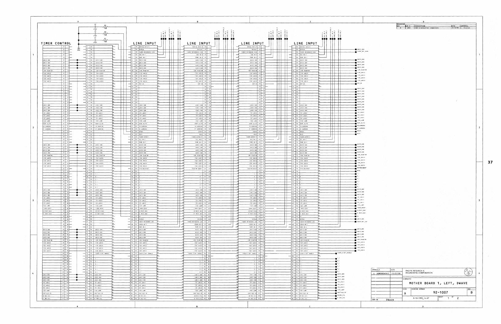
-
-
TIMER CONTROL ~----------~+-~;~
'f-
PI \5 f--PI 16r-
PI H f--PI 18r-
PI 19 f--1'\ lOr-
PI 21 f--PI 2.Zr-
PI33-
1'134-
1'\ 35-
I't 36-
1'137-
PI 41_
1'11,._
1'1 ~O-
1'1 SI
P! 52_
PI55-
1'151,-
1'1 651--
1'1 ('6~
1'1 67r
PI nrPI 691--
PI 19 r--1'\ 8Cl
P! 81i
PI 821-
pt 83i-1'\ 54 i--
PI as f--PI 86-
-IS 1'2
-16 P2
-171'2
-18 P2
-191'2
-201'2
-211'2
-221'2
27' 1'2
- n 1'2
- H 1'2
-351'2
-361'2
-37 P2
-47 1'2
- U 1'2
-so P2
-511'2
-521'2
-5) 1'2
-541'2
-65 P2
- 66 P2
-67 PZ
_-68 P2
_69 PZ
-79 P2
-80 p2
-81 P2
-62 p2
-83 P2
-84 P2
-85 P2
-86 P2
"-,
I
-" - \61'3
23 pl L061CGND
24 1') LDG:C GN~
25 p) LD61CGND
-H
'--- " - 35 p] HD[R~IPERI
-" -"
43 Pl 'H •• AUDIO
U 1') 'In AUUO
- 4T 1'3 ·SUTE~ USET
58 1'3 'SYLOGIC
59 1'3 -5VLOGIC
-" - .. -67 Pl HDERREfERENCELOW
- .. -"
78 ?3 -16YAUDIO
79 1'3 fADERSTAR'ENABLE
-80 Pl r'-,
89 p3 LOGIC GilD
90 1'3 'SY\.OlllC
I
-161'6
-'- -151'6 FADER WIPER 4
-'- 1'536-- -" -; -"
41~"
,,-
run REFERENCE L(lW 1'5 6T r---.
78;---"'
PI, 80:- --" p; 80- -ao 1'6 "-"
,
83--
I
I
';VLOGlC
+5VL(lGI(
_12V_LAMP
KHP_ALIVE
eRItARNING
~UY_AUDl(1
nS,h_IlUET
.. ,.
·16YAUOIO
~U¥ AUDIO
"UY AUOIO
-16¥AUDIO
J
4361 3/10/99
- 37
--------.----.--------------------------~~~ A",.IQULS (J\~
J. DOMBROWSKI 1 1/2/98 ~~g~~E~~~~~~~tORAT10N ' \lEJ
MOTHER BOARD 1, LEFT, DWAVE
D '''''' .. " .... 92-1007
3-10~1999 14:27 2 DWave
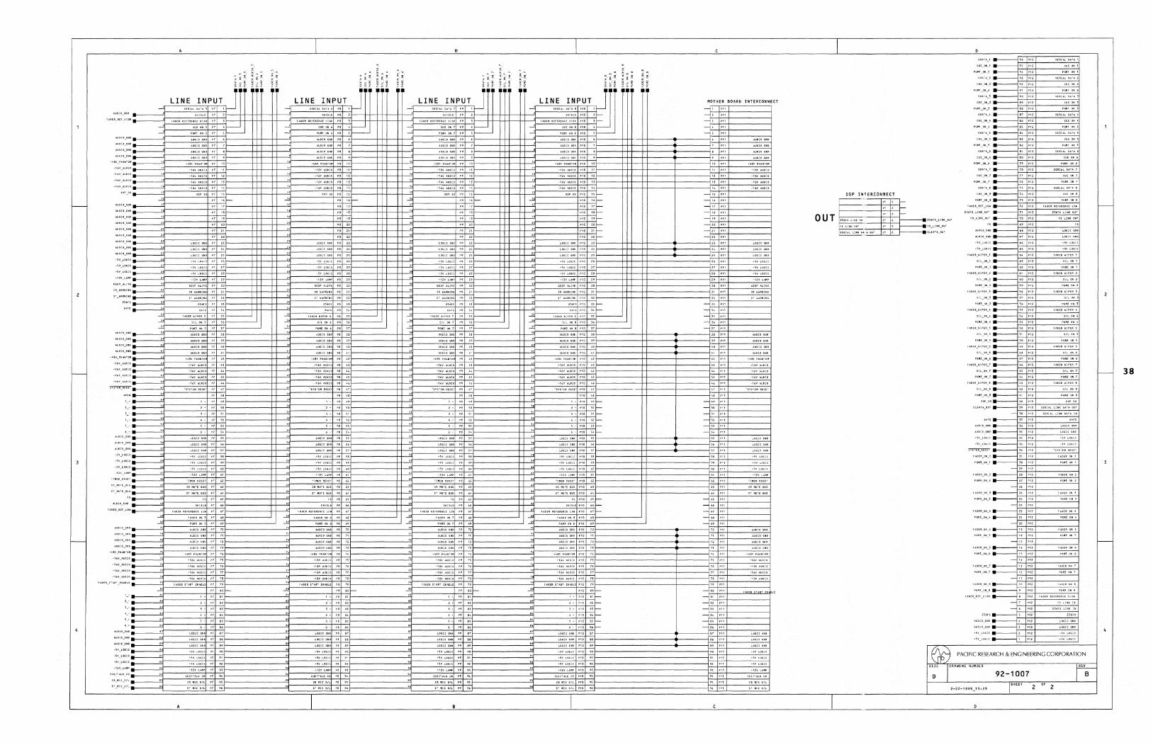
-
-
~UO!O_GNO
~U~! I) GNO
-I'Y AUHO
~'6V AUDIO
OGPGO
AUDIO_Gill
AUOIO_UO
AU'IO_GN~
·SVLO&lC
·'6YAUDIO
_'6VAUO:O
-16YAUDIO
hSlE~_RE5E
,,-..-
,,-
CUE/ULIC~CR
CR_lIlC_OIL
STIIlCO/L
--'
P7 16_
P71Sr---
AUDIO G~D P7 40
AUHD eNG P7 41
AUDICOND rT 70
AUO!OGND PT 7\
AUDIOGIIO P7 72
.16Y AUDIO PT U.
1'7 80 f--
.SV LOGIC PT 9~
CU£ITAL~ CR P7 94
CRMICGfL P7 9S
ST iUt OIL PT 96
--'
-" "
I
I
PI 16 r--
C~ WARNUG P8 31
ST WUN;NG P8 32
P83S-
AuDlOGND P8 n
AUDIOGND PI 40
LOGICGItD p8 ;6
LOGIC GIn PI 57
ra 80-
-'
-" "
: ~'
LIN.~",,~,~.P"~T, JI ,-,-
-' -_~------~~r-~~: _____
plO to
P916-
-16Y AUD~O
LOGlCGND P9 57 LOHC"GND
.Sv LOG:~ P9 sa
*5VL06!t P9 59
AUO:;:OGNO PO TI
P9 80 f-- ~t
LOGH GIIO Pt "
'SYLOO:C PO 90
-SY LOGIC n " -SY Loa:c P9 n
I
MOTHER BOARD INTERCONNECT
=~:-+~~--------~ -~'-+~r---------~ =~:-+~r---------~
-~'~'~~----------4 =~:~:~~----------4 =~:~:~~----------4
=~:~:~~----------4 -"
:::r.:~:~~----------~
:::~:~:~-r----------4 -"
:::r.:~:~~----------~ --~'-'~-r----------~ :::r.;7:~~----------~ -- ..
=E:~:~~----------~ -~'~'~~----------4 =r.:~:~~----------~
=r.:::':~~----"""""W'''''''''''CJ''''I'' " --~~~~r----------4 :::~::-+~r----------4
=E:::':~~----------~
I
-OUT
- 38
~ PACIFIC RESEARCH & ENGINEERING CORPORATION
SIZE I '",W"6 NU.SER
92-1007 D ISHEET 2 OF 2
I
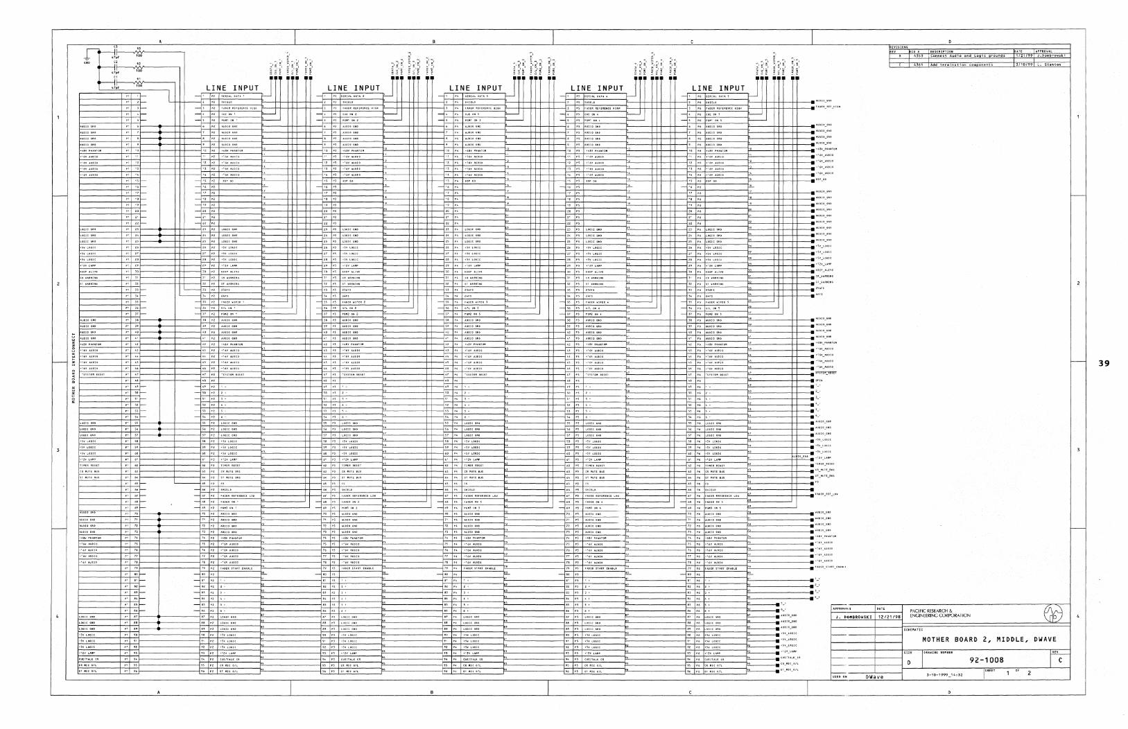
-
-
I'~-1" iil-~NV-__ --.
47pf
" ~t"I-----~~-------'
1--------++--:-1; ~ 1-----------+--1~'1--1-------+--+--:-1; r=
" 1,t-
.' "r_ -, I--"I--
" '9 f--
" "r_
" "r_ " "r_
1--__________ I--4-'~'r-p, H t-
1------------I--,,4-:~:~ p' 37 f--
P' <9-
I------------r-e,+-:~~==
I-----------+~-,~':== ,,-
--, e' --, " -" e, -'0 " -" " ->0 e' -2' " -n "
-33p2
-,4P2
-35 p<
-,. " -H P2
- 49 p~
-,0 P2 2-
-5'
-52 P2 4-
- n "2
-54 P2 6
1------------1--+-:4:== -" - ~6 P2
I----------~r-+-'~'-1------------1--,,-1. ~::==
- 67 P2 FM~R REfE~EN<;c LOW
-6a POl
-69 P2
p' 80r- -80 P2
I------------r-•. +-:~;r= -~. p2
-e2 P2 <'
r' e3~ -83 P2 3,
1--__________ I--4-.~'r-1------------1--,,+-:4: ~
- 84 P2 ~ t
-as P2
- ~6 P2 6 t
P2 t s~ l.OGI<
I
c;-- --, " ~
- 35 p~
-36 P:I
- ~7 PO
-68 P3
-69 p3
-80 P3
1
-
-35 P4
-36 P4
-;17 P4
'39 PI.
-68 P4
-69 P4
-BO P4
~
"----. "---. ,
I
I
- -'6 P6
-35 P5 -3, P6 FADERWIPERS
-36 P5 -,. - F PS -H
-68 PS -M
-69 P5 1"--------------' - ..
79 P6 F'\DoRSI,\RT ENABlE
-8Q p, -80 P6
I
I
"6VAUQIO
~
REVISIONS
m
~------+-----4
" . 4353
4361
Connect Audio and Logic grounds
Add termination components
OATe 1/21/99
3/10/99 L. Stanton
MOTHER BOARD 2, MIDDLE, DWAVE
1---- -----1------1 \""'" ""'" 92-1 008 ~ I---.-===~==~D~==~~_pm-'''Z--~I~ ~ f---. ISHEET 2 usn Oil DWave 3-10-1999_14:32 I
-
39
-
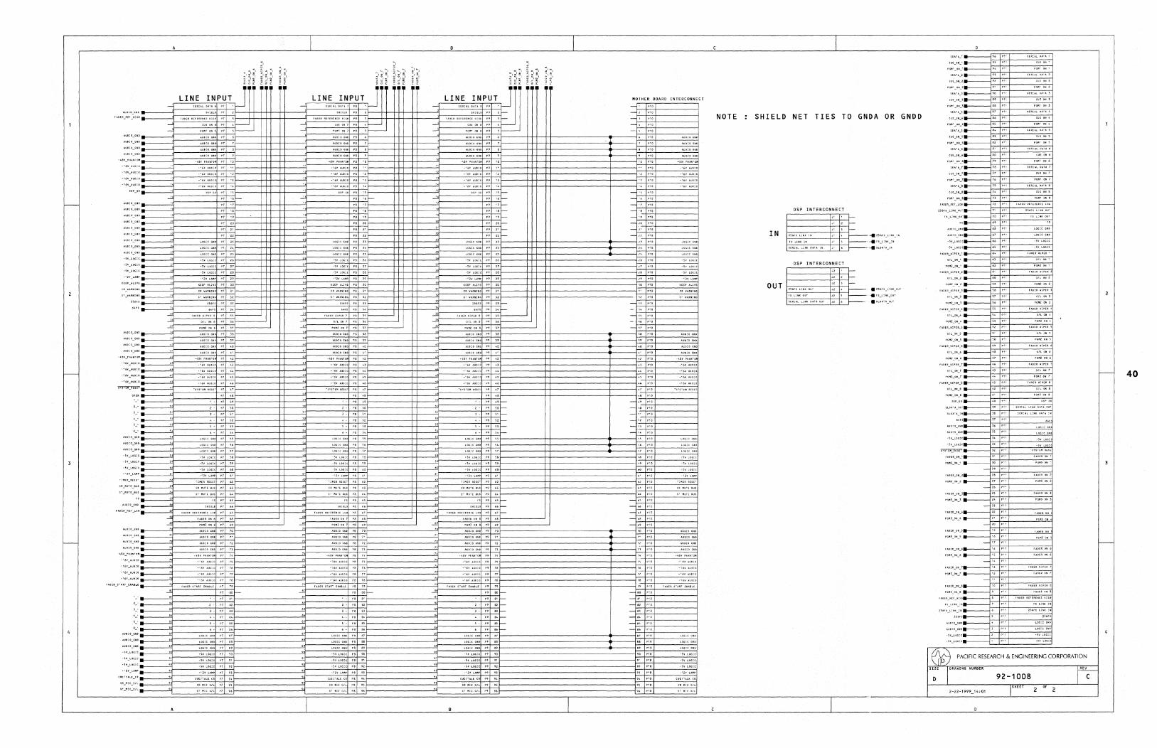
-·'oV,\UD:O
"~-U~_kESE'
'-
'-
.7 16L--.
""-
--" P780-
"
I
"-
P83,-
-,VLOG,C P8 58
SHll'li PB 66
''\~€R S',R- £N,\On PS 79
P880-
'>
P916-
"
P918-
P9 '9 t--P9 20!-
p9 21rP9 221--
"rHC-
P9 3Sf----
(;iLON8 r9 36
P949_
>0-
,,.9 S2-
n"9 H-
,,,,-
fAD"RRHERENCELOV P9 67-
r9 60f--
"9 S', I--~9 82r
r9 el-
p~ 64 r--P98,
P986-
I
I
MOl'HER BOARD INTERCONNECT
:r;++-----I :~:-+~--------_1
:f--f--f------j
:~:~:~~----------~
:r,.--+-c+-----I
:I-'-::+-:+------j
-r'-'~~--------__I
-1:'':-' +-=-+-----.j -H I""
- ,'+-'+-----1 -' _ ",C-, ~~--------__I
=I~t=-f------I
=r::-' ~+-------~
:~:~:~I~",~----------I -"
:~:~~~~-----------1
-~'~'~~-----------1 =r:~:~~-----------I -~:~:-i,~",o~---------.j
NOTE SHIELD
IN
OUT
I
NET TIES TO GNDA OR GNDD
DSP INTERCONNECT
D5P INTERCONNECT
f-___ ++-jr-f----++-j~
40
-
~ PACIFIC RESEARCH & ENGINEERING CORPORATION
Ic SIZE IDRA'ING NUNBER
92-1008 D
2-22-1999 14:01 SHEET OF 2
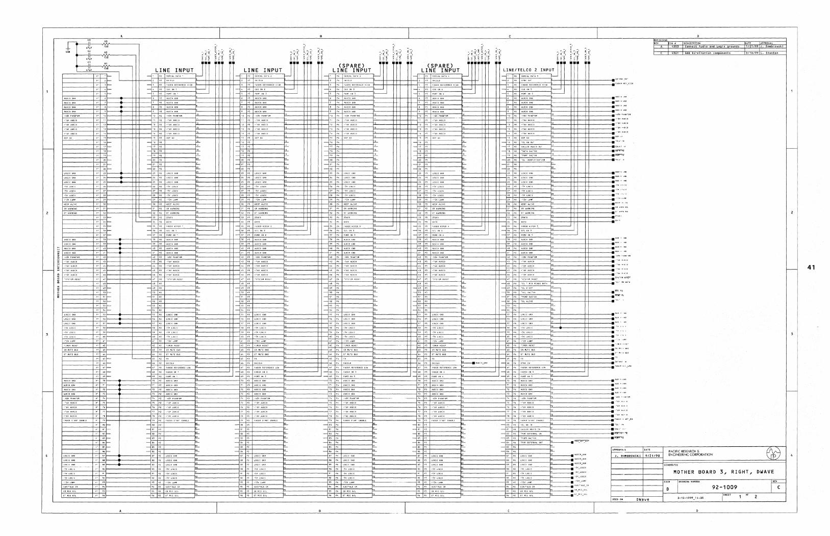
-
-
'r-r------------~~~,r__
~----------~4_~:~ or--
" r__ " r__ "1-
" "I-e' <or__ e' ,. ,-eo <of-
P' H-
r__----------~,,~;~:== p' ,6-P137-
I-----------~+-:~:== S'-
f------+'-" 1-'-1" _ r' 53-
;;-
p1 Q; I--P1 6'rP1 671--
I-----------~e-+-:~:~
I----------~~-:~~"= I---------~~+-.~'-
~----------~4_:~:== f------+-+.,-1.', -.. -
.. I'"
LINE INPUT -, " SERlAL DATA ,
-, e, 'AO£R ReF EREN~E H I Gil
-, -,
- ., e' - H eo
- ., eo
- " " ->0 e' -" e' - " e,
L---;3 P2
L-34P2
- ~5 P2
- H Pl
-37 P2
-49 P2
-SO P2
-,1 P2
-" " -53 P2
-54 P2
-65P2ru
- 6~ P2
- 67 p~ FADERREF,RENC, LOW
-68 P2
-69 P2
'AHR ,-AR- ENABLE:
-00 "' -" -" "' -" " -M " -" "' - .. "
, .. I;;;
J ~I
,
'--;-----
f.L f!-f.L P-F-'--r:-r;-
I"-I"-F'-~ I"-F'-e-
I
N
~I:I ~I
- ,L~NO:",~.~,PUT J"T e<
1-' 1->
-1-" " 1- 00 " 1-" eo
1- 00 e' 1-" 1-" "
.-~~--36 p!
'-37 Pl
-" " -," "' -0'
-" " -;, " -;0 "
-68 PJ
-69 Pl
-.0 "' -,. "' -" "' -" n -M " -" " - .. "
fAHR ~rFEUUCE ulGH
r--I'-----
r'--f!-f'--r'--f'--r:-r;-
"-"--"-"-"-"-,
r~p<R S-~RT ENABLE
I"-I"-F'-F'-I"-!"-"-,
N
"'I :1 , ,
J (SPARE) LINE INPUT
-, e< HRlAL DA"A,
FADH REFH,NCE HI<HI
-, r---, f--
- " N f-'--- " " f-'--- ., N ~ - " e' f-'---00 e, "--,. r'--" " ~
-35 P4
-36 P4
-37 P4
-" " "--," " P--,- " I"--" " I"--" eo I"--;0 " ~
1-68 P4
1-69 P4
I" " -00 " -81 eo
-" " -" "
~~-+----------~~ "~~~-----------{"r "-
-" " F-f"--f"------1."-.
-" " - .. " "
~~-+----------~"-,
I-- '
,- " " -'-- ., eo "-- .,
" -'-,- ., eo -'-'- 00 " "-,- ,. e, "--- « " '!-
,'"""''"'
-35 r5
-J7 P5
--- -38 PS
F'--" " F'--," eo f'---,. F'--" "' f'---" " P--;0 "' P-,
I--- H P5
1- 69 PS
--74PS
I
-80 P5 fL -~,~,~,,-+----------->~ - 83 p, fL-- 84 PS fi--" e; F'-- 86 p, F-,
-" e' _., " _., "
_19 e, -00 " -" e' -« e'
-35 P6
-36 p6
-37 PO
1- " " 1- " "' 1- '" " 1- " " ,- " eo
i- " " ,- ;0 e'
-66 P6
-68 r6
-69 P6
-80 r6
_8' P6
-82 p6
-83 P6
"Cl :H~T:F!cAflON
'[L' MIX ~INU. BOTH
- 84 PO -PORH-ERN'LOU~
fa-
I"-e-
-" eo F'-- 86 P6 p!-
"
I
I
"..-"
~.
,,".'rIlHTI'T
,,"
" , 4353
4361
DATE
Connect Audio and Logic grounds 1/21/99 J. POlllbrowsl:.i
Add term i nat i on componetl t s 3/10/99 L. Stanton
-
~;~-.-,------.-------r--PA-C-"-'C--RE-SE-A-RC-H--&----..---------------------O\7'",",,~:--I
1-;:-;';'-.8-'O-'-S K-' +-. ,-, -"-9B-1 ENGINEERING CORPORATION ."JEJ_ SCllEMArlt
MOTHER BOARD 3, RIGHT, DWAVE
f---- I""''' '''''' 92-1009 Ic _. 0
DWave 3-10-1999_14:35 I SHEeT 2
41
I--
I--
~U[I"lK_CR
(~ "H Oil
,.f-
"'''''""''0"' " "f-"AUlD ,WITCH P7 '8 t--"PGII1 SVITCH P7 '9t---
IOENTlfICAT-I(IM P7 20 I--
.--l~ fADER VIPER 6 P7 3,
--' --'
P749t-
f7 sof-P7 "f--
"f-
,"-
ULHR AU~IO U p7 81 t---'POR EXTERNAL IN P7 82 f--
-PO~ fXTER~AL OUT P7 84 I--
I
"8 '1st--P8 36t-
P6 37/--
P8 68r-
F.DH SIIRT <NA8L.E pt 79
fa 80 f--PG~2 OUl L + P8 6'
I
--' --' --'
P9 161---
p9 3Sr---
P9 36 r--P9 37f---
P9 68:--
f9 aD~
,.f-
Hf.f------~~"i"f-
.. f-
T
I
'---J.
:: '---J. ';-
~,I;';;;-:. ---~f--:-'-I: =--. 16 ~H'H. 'S ---4
'.--< " f-----<
n S~IH" 23 lOG], U~D
" 2S coal' ~"D
2 'SVlUGlC
<7 ,~v L no! C
28' sY ,,,nH
" f-----< "r---
--" , ____ -+'---f-'-d-....l2f-- 32t----1..3 ~; I----1.4 DI~Pl-4T vurpp~
....1.5 ~~STH FADH W1PER 2
-1.6 -PG~211'G~3
--" "
42 <48V ~UNTD"
H+<6V;'UDIO
4'_'6'.UOIO
47·snTt " RUEl
46 lEl • 'UX ~INUS BOTH
S paMI <>UT ~ _
5' PG~~ I>Ul R
52 PGM\,,'" R-
54 t~!.< ~UQIO _
" , L.OGI t ~ND
57 l061 C ~Nn
58 'SY L,u~1C
74 '; e. rM~NTO~
75 " /" ~"Dlo
79 f~OI~ ~I~RT EN~aLE
",S ,. '"
:: l------l ::f-.-J "f'"f"f;of-0' f"f"f"I--
::f--J .....§! P1" eo f--
8' ~O"I (>01 L ' 8' f--
::~~ :::~:'-: .:.: -: --+-+-=:"-1: ~ 8. P6~\ ",,( R t 84 f--8, H~~I\AlL"R ' 85 f--6 86 '--
::---l .. -----1
_J...4 94-
~,.f-----------~+~"f-.....2. 96 f--
I
NOTE : AUDIO CO""ON AND LOGIC COMMON ARE TIED
IN
TOGETHER ON EVERY MOTHER BOARD.
DSP INTERCONNECT
~Ik"
" , " ;
2S6FS LINK IN ,'4 2,6FS_LlNK_I~
FS UNK I~ <' , IS ~lNK IN
SERlAL L!NK DAH I" "-" 6 SL~ATA_IN
~ PACIFIC RESEARCH & ENGINEERING CORPORATION
SIlE I DRAWING NUMBE.
92-1009 D SHEET OF 2
I
42
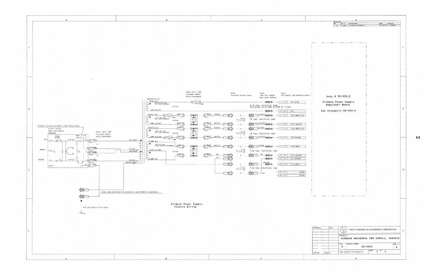
InternaL Fuse not provided in Power Entry ModuLe
PSOSXSS30
GROUND
•
WHT 115Vl
YEL eVl
ORG 41SV2
BLK eV2
GRN/YEL 7 ESS
AWDTRAN 48-124
49V38
• 0.12A rms t)'p. 49v rms unLoaded
MoLex .250 x .032
insuLated female
Qui cK Di sconnects
M30
MoLex MoLex MoLex
InsuL.ted EyeLugs 18awg .093 HIGH CURRENT
MALE CRIMP TERMINAL
3191 SERIES. 096 RECEPACLE,12PIN
---1 1 I P1 I 45v unreg
0.1A. typo resistive load following fw bridge 8. 1000 uF filter
~~OV~~~G~RY~I~'h~' _______________________________________________________________________________ ~ -~L~2~1~~~o,~,~ ______ ~
22V410 VIO
• ~-"""--,V-"lO,,-I,,,<H,,-T __________ --i=Q09 I
~2~2V~5~'2~8~LV~E ____________ --i=~~ ~
•
OV6H 'wlH/GRN
• 1S.8V1li GRN
-~'."-... '"
- .
:~: ~ -~'." .. ~
m
~+9 <HT~ "Iil> ~-~ WHT _
~
~~~ '--'--------e
-~ -~L"':''-ll~p~'~---=-''~'~V...:V~NR~E~G~:..:..J 1A typo resistive load
_~,'WHT/~RED .... -~~ -~L~4~I~p~'~~"~'_V~RE~T~VR~N~~
-~, BLU/BLK .. _ ~.~ -~L~ll~p~l~ __ -l~'~V...:V~NR-,E~G~P~LV~S~
1A. typo resistive load
-~ -~L~6--,-! ~P~' .J.1 ___ -l:c:'.:.Vc:Rc.ET:c:Vc:RN'-----------l
-~ ---1 7 I P1 I +12V UNREG
7.SA. typo resistive load
-~~------18! +12 V RETURN
-~~=9~I=p=,~=='5==V=R=ET=V=RN====
7.SA. typo esistive Load
--1_~El _________ ~ --1 12 I Pi I UNUSED I
Note: ESS termination not provided in split-bobbin transformers
#10 stud Chassis Termination
AirWave Power SuppLy Chassis Wiring
initiaL schematic
Assy # 95-955-3
AirWave Power SuppLy ReguLator Board
See Schematic 92-955-3
DATE
2-19-97 T. Staros
P.~CIFIC RESEARCH & ENGINEERING CORPORATION
AIRWAVE UNIVERSAL PWR SUPPLY, CHASSIS
D 92-1015 A
1 OF
L-__________________________________________________________ -, _________________________________________________________________ . _____ ,-____________________________________________________________________ ~-----lv~S~ED~O.~_~~~~ ____ ~L_.'_'_s_._"_d_'_9-_'_'-_1_99_8-_'_0_"_6 __ ~ ______________________ ~
43
-
I---
MoLeK
3191 SERIES .096 RECEPACL.E,lZPIN
4Sv unreg 1 J, 1 ' f--
1 J' 1 2 f--
! TIP122
R7 3• 83
., 19 34K
R18 4.7K-1'2W 237
'" • rIN475'"
4711 1W
'"
I
17.71/
---i ' 1 j 2 1 45v phanto.
MoleK
3191 SERIES .096 RECEPACL.E,12PIN
'~r't"".. -+ "'", L-________________ ~ ____ 4_ __________ 4_ ______________________________ _4 _____________________ -------__ ~~~ - - ~L~3~_J_2~1 __ ~Ph~.~"~to~.~,~0.~'~0~n I
"IC295028T
+1811 UNREG PLUS! Jl I :5 t- - ---<':~!3'I=----------------------------------t__._-_'jl~, I"
"" 29502 1 16.24 V typ1eal ourr~--~----~------------------~----------------~------- -------__ -€~~=r-",I
+18 V RETURN
-18V UNREG PLUS
-1a\l RETURN
+12v UNREG
L_.':12 V RETURN
+5 V RETURN
'5 V UN REG
["RESERVED J1Rl1
I" ME SERVED J1-12
I 17.711
~1.21K lK-1W
i ... 6 3
i~.fin, US :~~PS2506
.' 5 4
"'IC295028T 38.3
I MIe I Jl I 5 t-- - ---<':=_3l==-------------------------------~-.---'jl zl" 29502 ouTr~k---'6~ . .:."--V-t.:.yp.:.'-'-.l----..._-----l-----_+---------------~----------+_----. ...... -E'7-
I" ,,,I ~ 1R~~ L[', ---,;:---;: !",:- ?,.21K
~
~1O. I I 'r I J' 1 6 f-- . --E=~~~~----------------------------J----------l---------~------~----------------~--------------J---------~----~~-~=>-
J, I 7 f--
J1 8 f--
J, 9 f--J, ,. f--
J' 111 f-J 1 12 t---
"'IC295028T
J Mle I -E= .... ~.,... ....... ------------------------------..,...----_'l~.rIN 29502 OUT~ 12.24 II typlC.ilt
l" '" 1 '
E$'
~'
I
l-___ TJ, ---';-~i " f 887
~ j
IIIIC29712BT
~, .. !
12.23v
-." .l vout = «r1/r2 )+1) * 1.24 2~712 5.35 V typic.al
OUT~--~~----_.----------------------_+----------------------~--~~~'=3-",I I" 5.16v
"
Eaperic.alLy, .. e.sured 59* C c.ase Q1 4A wI 23. C Imbient~ bloc.ked botto. ventllatton 14/ 2.6v •• rgin at 6.5A, & 2* C/W, that is I 34* Crise 59 + 34 .... C= 93* C. A urgin of 27"'" C below lUX Junc.tton te.p. Thh would imply that aMbient te.p could be IS high as SO* C Max operating te .. p is still U.lted to 40* C
- . ---i 2 1 J2 + Audio
- . -1 4 1 J2 1
- - -1L~5:..J._J:.:2'-L1 ___ -"''"::'c:' o:...::oo::,::c,o:::"'-.I
- - -1 6 1 J2 - Audio
- - ---1 7 I J2 I +12v Logic/Limp [
---i 12 J2 Logic COillon
-1 9 J2 L.ogic CODllllon
-1 8 J2 +5, Logic
--1 J2 AUDIO COMf'lON
----1 10 J2 RESERVED J2-1Z
I
Af>"'/I'OVALS DATE
I-
I--.---t----l
COli IIESCRIPTION
no e In hL es1 n MD-181 JIIfg Dell adj. up 511 to 5.3511
9-2-98 T Staros 1Z14/98 T. St.ros
~ PACIFIC RESEARCH & ENGINEERING CORPORATION
§CHE"'AflC
AIRWAVE UNIVERSAL PWR REG. BOARD r-,-------4----~
r-'--_-_-_-_-_-_-_-_~-----------_1-+O"'~zD~E---rro'~RA~W~IN~G~N~u~"8~e~.-------------------------~~"~'-A--i I 92-955-3 I A
" U1H~ ON
I I --------------~I
AirWave
44
::E=!&E has a full line of logic oables designed
for use with the AirWave Digital console and the
QuikBilt II modular cabinetry. QuikBilt II cabinetry
is economical, rapid-assembly, studio furniture de-
signed for use with the AirWave console family.
QuikBilt II cabinetry can be configured to create
individualized studio furniture packages in either
stand-up or sit-down styles.
PR&E's PrimeLinefurniture line can also be used
with an AirWave Digital console. PrimeLine offers
pre-assembled cabinet components, in stand-up
or sit -down heights, with pre-cut console and wir
ing access holes. PrimeLine cabinets can also be
factory pre-wired since the cabinets are shipped
blanket-wrapped via van line.
BUTTON ENGRAVING
Input modules, and the optional Telco modules,
come standard with their red and yellow button
caps engraved ON and OFF. Custom engraving
on the button caps can be ordered at the time of
purchase, or engraved replacement button caps
can be ordered at the time of installation once the
input sources have been determined.
Each button cap can have up to two lines of
engraving with up to four alphanumeric charac
ters and a V2 character punctuation divider (space,
period, hyphen, slash, backslash, etc.) on each line.
Engraving is normally done on the yellow but
ton cap to identify the A input source on the top
line and the B input source on the bottom line.
Custom engraving is specified when a blank but
ton cap is ordered. For a yellow button cap, order
PR&E # 25-872. For a red button cap, order
PR&E # 25-871. For a white button cap, as used
for the Talkback button, order PR&E # 25-870.
FADER KNOBS Input modules come standard with white fader
knobs. The optional Telco modules come with
black knobs. Various colored fader knobs are also
available. The table identifies the PR&E part num
bers by knob color and typical source.
PR&F# Color SOl,ree
32-710-1 black Telco
32-712-1 red Microphone
32-714-1 yellow Cart decks
32-715-1 green CD players / turntable
32-716-1 blue Cassettes / reel-to-reels
32-719-1 white Remotes
32-720-1 gray Other Studios
32-721-1 orange Multitrack channels
PACIFIC RESEARCH & ENGINEERING
Revision A • 3/99
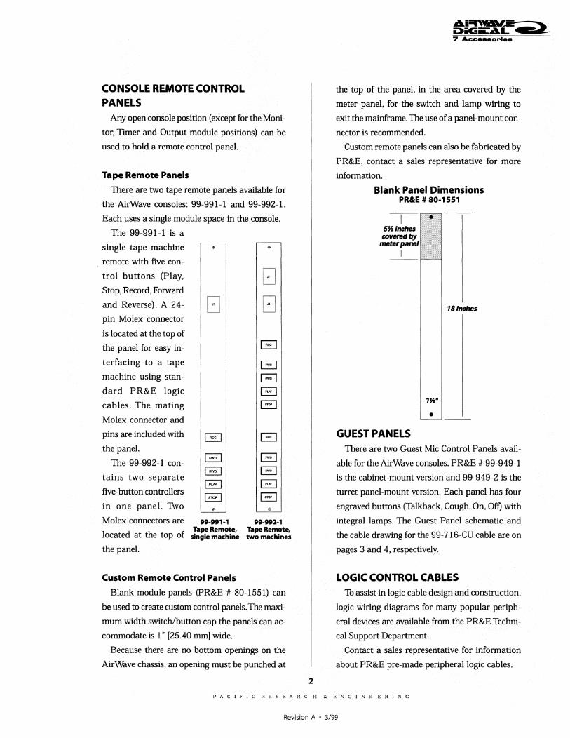
CONSOLE REMOTE CONTROL PANELS
Any open console position (except for the Moni
tor, Timer and Output module positions) can be
used to hold a remote control panel.
Tape Remote Panels
There are two tape remote panels available for
the AirWave consoles: 99-991-1 and 99-992-1.
Each uses a single module space in the console.
The 99-991-1 is a
single tape machine
remote with five con
trol buttons (Play,
Stop, Record, Forward
and Reverse). A 24-
pin Molex connector
is located at the top of
the panel for easy in
terfacing to a tape
machine using stan
dard PR&E logic
cables. The mating
Molex connector and
pins are included with
the panel.
The 99-992-1 con-
tains two separate
five-button controllers
in one panel. Two
D
Molex connectors are 99-991-1 99-992-1 Tape Remote, Tape Remote,
located at the top of single machine two machines
the panel.
Custom Remote Control Panels
Blank module panels (PR&E # 80-1551) can
be used to create custom control panels. The maxi
mum width switch/button cap the panels can ac
commodate is 1" [25.40 mm] wide.
Because there are no bottom openings on the
AirWave chassis, an opening must be punched at
2
Ai=t\~;;:-=---... i>iCSiiLAL"" > 7 Acce •• arlee
the top of the panel, in the area covered by the
meter panel, for the switch and lamp wiring to
exit the mainframe. The use of a panel-mount con
nector is recommended.
Custom remote panels can also be fabricated by
PR&E, contact a sales representative for more
information.
Blank Panel Dimensions PR&E # 80-1551
-1-5~;nches covered by
meter panel
I
GUEST PANELS
1Binches
•
There are two Guest Mic Control Panels avail
able for the AirWave consoles. PR&E # 99-949-1
is the cabinet-mount version and 99-949-2 is the
turret panel-mount version. Each panel has four
engraved buttons (Talkback, Cough, On, Off) with
integral lamps. The Guest Panel schematic and
the cable drawing for the 99-716-CU cable are on
pages 3 and 4, respectively.
LOGIC CONTROL CABLES To assist in logic cable design and construction,
logic wiring diagrams for many popular periph
eral devices are available from the PR&E Techni
cal Support Department.
Contact a sales representative for information
about PR&E pre-made peripheral logic cables.
PACIFIC RESEARC H & ENGINE ERING
Revision A • 3/99
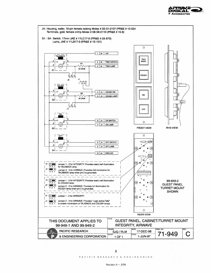
J4: Housing, wafer, 10-pin female locking Molex It 22-01-2107 (PR&E # 15-524 Terminals, gold, female crimp Molex It 08-58-0110 (PR&E It 15-8)
S1 - S4: Switch, 17mm JAE It 11LC17-0 (PR&E It 25-873) Lamp, JAE It 11LB17-0 (PR&E It 12-101)
51L--1 123
J2 Jl
I I 52---
J,3
I I 53 __ _
I I 54---
r-----------------J2 10 _I Jumper 1 - 2 for INTEGRIIY. Provides static half-illumination
I 3 2 1 forTALKBACK lamp.
I J2 1- 01 Jumper 2 - 3 for AIRWAVE. Providies full-illumination for 3 2 1 TALKBACK lamp when pin 3 is grounded.
~--------------~-~ r-----------------1
J3 10 -I Jumper 1 - 2 for INTEGRITY. Provides static half-illumination 3 2 1 for COUGH lamp. I
IJ3 1- 01 Jumper2-3forAIRWAVE.Providesfull-iliuminationfor I 3 2 1 COUGH lamp when pin 5 is grounded.
~----------------~ r-----------------Jl 10 _I Jumper1-2forINTEGRIIY. I 3 2 1 I I Jl 1- 01 Jumper 2 - 3 for AIRWAVE. Provides "Logic Active Tally"
3 2 1 to enable illumination of TALK BACK and COUGH lamps. I ~----------------~
o
B [:]
B 0
FRONT VIEW
0
• o
o REAR VIEW
RHSVIEW
99-949-2 GUEST PANEL
TURRET MOUNT SHOWN
THIS DOCUMENT APPLIES TO 99-949-1 AND 99-949-2
GUEST PANEL, CABINETrrURRET MOUNT INTEGRITY, AIRWAVE
1-JUN-97 c 1 OF 1
PACIFIC RESEARCH 17-DEC-98
& ENGINEERING CORPORATION 71-949
3
PACIFIC RESEARC H & ENGINE ERING
Revision A • 3/99
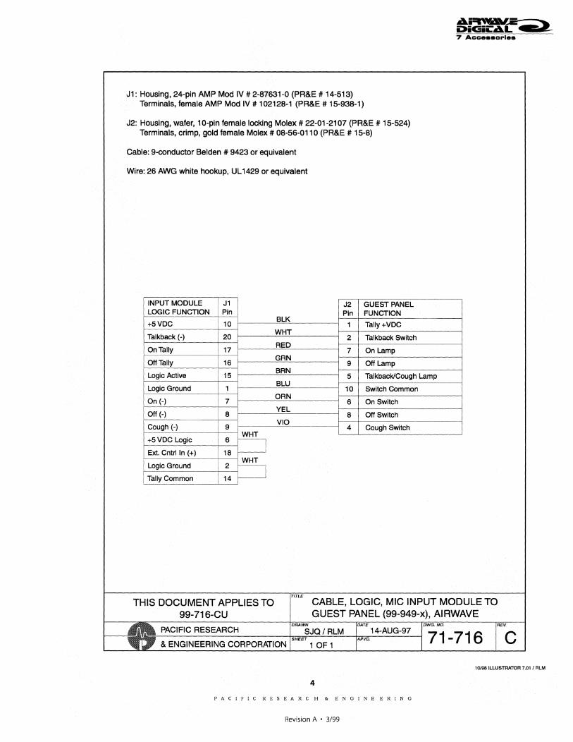
J1: Housing, 24-pin AMP Mod IV # 2-87631-0 (PR&E # 14-513) Terminals, female AMP Mod IV # 102128-1 (PR&E # 15-938-1)
J2: Housing, wafer, 1 O-pin female locking Molex # 22-01-2107 (PR&E # 15-524) Terminals, crimp, gold female Molex # 08-56-0110 (PR&E # 15-8)
Cable: 9-conductor Belden # 9423 or equivalent
Wire: 26 AWG white hookup, UL 1429 or equivalent
I INPUT MODULE I J1 I J2 GUEST PANEL I LOGIC FUNCTION I Pin Pin FUNCTION
+5VDC I 10 BLK
1 Tally+VDC
Talkback (-) 20 WHT
2 Talkback Switch RED
On Tally 17 7 On Lamp
Off Tally 16 GRN
9 Off Lamp
I Logic Active 15 BRN
TalkbacklCough Lamp 5 BLU
Logic Ground 1 10 Switch Common
! On (-) 7 ORN
6 On Switch
I Off (-) 8 YEL
8 Off Switch VIO
Cough (-) 9 4 Cough Switch
I WHT +5VDC Logic 6
! Ext. Cntrl In (+) 18
I Logic Ground WHT
2 I I Tally Common 14
THIS DOCUMENT APPLIES TO ITiTLE
CABLE, LOGIC, MIC INPUT MODULE TO 99-716-CU GUEST PANEL (99-949-x), AIRWAVE Ell: PACIFIC RESEARCH IO~SJQ I RLM IDATE 14-A.UG-97
IDWG. NO. REV.
71-716 C & ENGINEERING CORPORATION ISHEET 1 OF 1 . IAPVD.
10/98 ILLUSTRATOR 7.01 / RLM
4
PACIFIC RESEARC H & ENGINE ERING
Revision A . 3/99
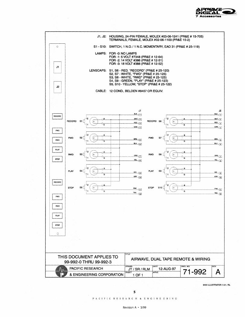
o
II RECORD I 51 q RECORD
G G FWD 52 q
G 53 q RWD
B PLAY 54q
II RECORD II
5TOP
G G G B
c
L 11
..a.i~~=-:---ii>iGii:'..a.rr=- > 7 Acc ••• arl ••
J1, J2: HOU5ING, 24-PIN FEMALE, MOLEX #03-06-1241 (PR&E # 15-705) TERMINAL5, FEMALE, MOLEX #02-06-1103 (PR&E 15-2)
51 - 510: 5WITCH, 1 N.O. /1 N.C. MOMENTARY, EAO 31 (PR&E # 25-119)
LAMP5: FOR -0: NO LAMP5 FOR -1: 5 VOLT #7348 (PR&E # 12-64) FOR -2: 14 VOLT #386 (PR&E # 12-51) FOR -3: 18 VOLT #388 (PR&E # 12-52)
LEN5CAP5: 51,56 - RED, "RECORD" (PR&E # 25-120) 52,57 - WHITE, "FWD" (PR&E # 25-125) 53, 58 - WHITE, "RWD" (PR&E # 25-125) 54,59 - GREEN, "PLAY" (PR&E # 25-123) 55,510 - YELLOW, "5TOP" (PR&E # 25-122)
CABLE: 12 COND., BELDEN #8457 OR EQUIV.
BLK cJ..o
a WHT--f2l
/0 ) RED 3 b
GRN--I4l
RECORD 56 q 12
11
a
tl b
BLKcJ..o
WHT-f2l
RED-l3l
GRN-f4i
12(EJ a
BRN-uu ]1 ~ b
I
FWO 57 q 12~ a
11 F) BRN-ill b
12 a
Fl -] 1 b
12 a , fo J
11 b
12 ,a
I
BLU -i6l
ORG-{7l
YEL-uu
Via 9
GRY---l1Ol
PNK [IT]
TAN [ill
BLU ~'6'
RWD 58 q j2~ a
11 1 ORG-IT b
YEL-L!..
PLAY 59 q 12(~ a
l1\~) VlO --f9 b
GRY-fiO
12~ ,~
( (' ) PNK--L11... 5TOP 510 rl
'-1 11 \.--./ TAN lliJ
THIS DOCUMENT APPLIES TO 99-992-0 THRU 99-992-3
AIRWAVE, DUAL TAPE REMOTE & WIRING
PACIFIC RESEARCH
1 OF 1 & ENGINEERING CORPORATION
12-AUG-97 71-992 A
9198 ILLUSTRATOR 7.01 I RL
5
PACIFIC RESEARC H & ENGINE ERING
Revision A • 3/99
Note: Page numbers Jisted as Chapter-Page.
A
A Input ...................................................... 3-2 AC Connection.......................................... 2-3 AES/EBU Connection ................................ 2-7 AirWave Digital Console
Block Diagram .................... ................. 6~2 General Information ..................... 1-1,2-1 Power Supply ........ 1-2,2-3,4-9,5-7,6-42 Specifications............ .......................... 1-3 Warranty ............................................. 1-5
Analog RLS .............................................. 4-7 Analog SIM ...................................... 4-2, 6-29 AMP MOD IV Connector ........................... 2-5 Audio
Cable Type ............................... ........... 2-5 Connector pinout ................................. 2-6 Reset ........... ; .................................... 2-13 Wiring, General ................................... 2-5
Auto, Timer ............................................... 3-8 Auto-Feed ................................................. 4~4 Auxiliary outputs .............. ....................... 2-20
B
B Input ....................................................... 3-2 B Logic Interface .............................. 2-9,6-31 Bargraph Meters ....................... 2-20, 3-9, 4-8 Battery Backup .......................................... 2-4 Button Cap Engraving................ ............... 7-1
c Cabling ........................................ ........... 2-5 Clock
Option Switches .................................. 2-4 Setting the Time............ ...................... 2-4
Clock/Timer Assembly .............. 4-8, 5-6, 6-32 Control Room .................................... 3-7,4-6 Control Room Logic ................................. 2-21 Countertop Cutouts .................................. 2-1
vi
Crimp Tool................ ................................. 2-6 Cue ............................................. 3-2,3-7,4-6 Cue Speaker............................................. 5-7
D
Digital RLS................................................ 4-7 Digital SIM ....................................... 4-2, 6-30 Direct Outputs .......................................... 2-21 DSP .......................................................... 4-4
E
Engraved Button Caps .............................. 7-1 Event Timer ........................................ 3-8, 4-5
F
Fader Knob colors ......................................... 7-1 Replacement Part # ............................ 5-2 Service................................................ 5-5
Fuse Replacement.. ................................... 5-7
G
Gain Trim ............................. 3-1, 3-2, 3-3, 3-7 Grounding...................... .......... ........ ......... 2-3
H
Hold, Timer............................................... 3-8 Hybrid, Connection ........................... 2-19, 3-3
Input Module........ 1-1, 2-18, 3-2, 4-2, 5-5, 6-6 Input Module Logic ................................. 2-11
K
Keep Alive ........................................... 2-4,5-7
PACIFIC RESEARC H & ENGINE ERING
Revision A • 3/99
Note: Page numbers listed as Chapter-Page.
L
Level Meters ...................................... 3-9, 4-8 Logic
Cable Type .......................................... 2·5 Connector Pinout.. .......... ......... ......... 2-13 Interface .... .... .................. .................... 2-9 Guides .................................. 2-13 to 2-16
M
Mainframe ................................... 1-1,2-1,4·1 Configuration ....................................... 2~2 Grounding ........................................... 2-3 Installation ................................. 2-1 to 2-4 Module placement.. ............................ 2-2
Meter Panel ................................ 2-2, 3-9, 5-8 Mic Preamp Module ...... 1-1,3-1,4-1,5-5,6-3 Microphone, Connection ......................... 2-17 Microphone, Logic ......................... 2-10,2-14 Module Servicing ...................................... 5-3 Monitor Module .. 1-2,2-21,3-7,4-6,5-6,6-16 Motherboard .............................. 1-1, 4-4, 6-36
o
Off-Line Bus ....................................... 3-3, 4-4 Ordering Information .................................. 5-1 Output Module ... 1-2, 2-20, 3-6, 4-5, 5-6, 6-10
p
Parts Lists ................................................. 5-2 Peripheral Device Logic .......................... 2-11 Power Supply ........................ 1-2, 2-3, 4-9, 5-7
Grounding .................................... 2-3, 2-5 Schematics ........... ......... .......... 6-42, 6-43
Program Bus............................................. 4-5
R
Ready Logic ............................................. 2-11 Receptacle Contacts................................. 2-5 Recorder (To Tape) Connection ............... 2-19 Reference Levels...................................... 1-3 Remote Functions................................... 2-10 Remote Control Panels ............................. 7-2
vii
Ai=t\VAV!:=-:---'" i:»iGii:AL"' > Index
Remote Line Selector (see RLS) -Repair Services.. ......... ............................. 5-1 Replacement Parts ................................... 5-2 Reset, Timer .................................... 2-22,4-5 RLS .......................... 1-2,2-22,3-5,4-7,6-20
s
S/PDIF Inputs ........................................... 2-8 Servicing .......................................... Chapter 5 Shield, Cable .. ................. ........... .............. 2-5 Spare Parts Lists ...................................... 5-2 Spare Parts Ordering... ............................. 5-1 Specifications ........................................... 1-3 Start, Timer............................................... 3-8 Start Pulse ............................ ..... ............. 2-13 Stop, Timer ............................................... 3-8 Stop Pulse .............................................. 2-13 Studio Mic Connection & Logic ................ 2-14 Studio Warning Lamp.............................. 2-12 Switchboard Assemblies ................. 6-27, 6-28 SIM Cards ................................................. 4-2
T
Tally Outputs ............................................ 2-11 Telco Module ................ 1-2,2-19,3-3,4-3,6-8 Telco Operation ......................................... 3-4 Time of Day, Setting ................................... 2-4 Timer ................................. 1-2, 2-4, 3-7, 6-32 Timer Control....... 1-2, 2-23, 3-8, 4-7, 5-7, 6-33
u
Unbalanced Connections.......................... 2-8 Universal Power Supply ..................... 4-9,5-7
w --------------------------Warning Lamp ....... .................. .......... ..... 2-12 Warranty ................................................... 1-5 Wiring
Audio ................................................... 2-5 Logic ................................................... 2-9 Peripherals ............................ 2-13 to 2-16 Preparation .......................................... 2-5
PACIFIC RESEARC H & ENGINE ERING
Revision A • 3/99