digital voltmeter - bitsavers.org
TRANSCRIPT
8400A Digital
Voltmeter
Instruction Manual

P/N 314716 December 1971 Rev. 4 10/74
©1982, John Fluke Mfg. Co., Inc., all rights reserved. Lithe in U.S.A.
8400A Digital
Voltmeter
Instruction Manual
WARRANTY Notwithstanding any provision of any agreement the following warranty is exclusive:
The JOHN FLUKE MFG. CO., INC., warrants each instrument it manufactures to be free from defects in material and workmanship under normal use and service for the period of 1 year from date of purchase. This warranty extends only to the original purchaser. This warranty shall not apply to fuses, disposable batteries (rechargeable type batteries are warranted for 90 days), or any product or parts which have been subject to misuse, neglect, accident, or abnormal conditions of operations.
In the event of failure of a product covered by this warranty, John Fluke Mfg. Co., Inc., will repair and calibrate an instrument returned to an authorized Service Facility within 1 year of the original purchase; provided the warrantor's examination discloses to its satisfaction that the product was defective. The warrantor may, at its option, replace the product in lieu of repair. With regard to any instrument returned within 1 year of the original purchase, said repairs or replacement will be made without charge. If the failure has been caused by misuse, neglect, accident, or abnormal conditions of operations, repairs will be billed at a nominal cost. In such case, an estimate will be submitted before work is started, if requested.
THE FOREGOING WARRANTY IS IN LIEU OF ALL OTHER WARRANTIES, EXPRESS OR IMPLIED, INCLUDING BUT NOT LIMITED TO ANY IMPLIED WARRANTY OF MERCHANTABILITY, FITNESS, OR ADEQUACY FOR ANY PARTICULAR PURPOSE OR USE. JOHN FLUKE MFG. CO., INC., SHALL NOT BE LIABLE FOR ANY SPECIAL, INCIDENTAL, OR CONSEQUENTIAL DAMAGES, WHETHER IN CONTRACT, TORT, OR OTHERWISE.
If any failure occurs, the following steps should be taken:
1. Notify the JOHN FLUKE MFG. CO., INC., or nearest Service facility, giving full details of the difficulty, and include the model number, type number, and serial number. On receipt of this information, service data, or shipping instructions will be forwarded to you.
2. On receipt of the shipping instructions, forward the instrument, transportation prepaid. Repairs will be made at the Service Facility and the instrument returned, transportation prepaid.
SHIPPING TO MANUFACTURER FOR REPAIR OR ADJUSTMENT
All shipments of JOHN FLUKE MFG. CO., INC., instruments should be made via United Parcel Service or"BestWay"* prepaid. The instrument should be shipped in the original packing carton; or if it is not available, use any suitable container that is rigid and of adequate size. If a substitute container is used, the instrument should be wrapped in paper and surrounded with at least four inches of excelsior or similar shock-absorbing material.
CLAIM FOR DAMAGE IN SHIPMENT TO ORIGINAL PURCHASER
The instrument should be thoroughly inspected immediately upon original delivery to purchaser. All material in the container should be checked against the enclosed packing list. The manufacturer will not be responsible for shortages against the packing sheet unless notified immediately. If the instrument is damaged in any way, a claim should be filed with the carrier immediately. (To obtain a quotation to repair shipment damage, contact the nearest Fluke Technical Center.) Final claim and negotiations with the carric;r must be completed by the customer.
The JOHN FLUKE MFG. CO., INC, will be happy to answer all applications or use questions, which will enhance your use of this instrument. Please address your requests or correspondence to: JOHN FLUKE MFG. CO., INC., P.O. BOX C9090, EVERETT, WASHINGTON 98206, ATTN: Sales Dept. For European Customers: Fluke (Holland) B.V., P.O. Box 5053, 5004 EB, Tilburg, The Netherlands.
*For European customers, Air Freight prepaid.
John Fluke Mfg. Co., Inc., P.O. Box C9090, Everett, Washington 98206
Rev. 6/81

SECTION
1
2
3
TITLE
INTRODUCTION AND SPECIFICATIONS
1-1. 1-16. 1-19.
Description . . Specifications . Accessories
OPERA TING INSTRUCTIONS
2-1. Introduction 2-3. Installation . 2-5. Repackaging For Shipment 2-7. Options and Accessories 2-9. Input Power Requirements 2-11. Operating Features 2-13. Measurement Instructions . 2-15. External Reference 2-22. Remote Control Unit 2-33. Data Output Unit 2-51. Operating Notes
THEORY OF OPERATION
3-1. Introduction . 3-3. Block Diagram Analysis 3-25. Circuit Descriptions . .
8400A
Table of Contents
PAGE
1-1
1-1 1-2 1-8
2-1
2-1 2-1 2-1 2-1 2-1 2-2 2-2 2-4 2-6 2-7 2-11
3-1
3-1 3-1 3-4
(continued on page ii)

8400A
TABLE OF CONTENTS, continued
SECTION
4
5
6
TITLE
MAINTENANCE. . .
4-1.
4-5. 4-8.
4-30. 4-36.
4-50. 4-53.
Introduction
Service Information
General Maintenance
Performance Test .
Calibration Procedure
Compensating Component Selection
Troubleshooting . . . . . .
LIST OF REPLACEABLE PARTS
5-1. 5-4.
5-5.
5-6.
5-9.
Introduction .
Parts List Column Descriptions
Manufacturers' Cross Reference List Column Descriptions
How to Obtain Parts
Serial Number effectivity
OPTIONS AND ACCESSORIES.
6-1.
6-3.
6-5.
Introduction
Options . .
Accessories .
AC Converter, Option -01
6-1. Introduction
6-3. Specifications . .
6-5. Installation . . .
6-7. Operating Instructions
6-9. Theory of Operation
6-1 7. Maintenance . .
6-3 7. List of Replaceable Parts
6-39. Serial Number Effectivity
Ohms Converter, Option -02 .
6-1. Introduction .
6-3. Specifications . . .
6-5. Installation . . . .
6-7. Opera ting Instructions
6-9. Theory of Operation
6-20. Maintenance
6-42. List of Replaceable Parts
6-43. Serial Number Effectivity
ii
PAGE
4-1
4-1
4-1
4-1
4-7
4-8
4-11
4-12
5-1
5-1 5-1 5-2 5-2 5-3
6-1
6-1
6-1
6-1
1
3 6
9
1
1
2 5 5
(continued on page iii)

SECTION
6, continued
TITLE
Data Output Unit, Option -03
6-1. Introduction 6-3. Specifications . . . 6-5. Installation . . . .
6-7. Operating Instructions 6-9. Theory of Operation 6-28. Maintenance . . .
6-4 7. List of Replaceable Parts 649. Serial Number Effectivity
Remote Control Unit, Option -04
6-1. Introduction 6-3. Specifications . . . 6-5. Ins tall a ti on . . . . 6-7. Operating Instructions 6-9. Theory of Operation 6-23. Maintenance . . . 6-31. List of Replaceable Parts 6-35. Serial Number Effectivity
DC External Reference, Option -05
6-1. Introduction 6-3. Specifications . . .
6-5. Installation . . . . 6-7. Operating Instructions 6-9. Theory of Operation
6-19. Maintenance . . .
6-39. List of Replaceable Parts 6-41. Serial Number Effectivity
AC External Reference, Option -06
6-1. Introduction .
6-3. Specifications . . . 6-5. Installation . . . .
6-7. Operating Instructions 6-9. Theory of Operation 6-17. Maintenance . . . 6-34. List of Replaceable Parts
6-36. Serial Number Effectivity
Rear Input, Option -07
6-1. Introduction . 6-3. lnstalla ti on . . 6-5. List of Replaceable Parts 6-7. Serial Number Effectivity .
iii
PAGE
2
7 14
21
4
7
10
2 3 5 8
I
2
3 5 9
I
1 2
8400A
(continued on page iv)

8400A
SECTION TITLE
6, continued
7
8
10/18/74
True RMS Converter, Option -09
6-1. Introduction 6-3. Specifications .
6-4. Kit Installation
6-6. Operation
6-8. Theory of Operation
6-22. Maintenance . . .
6-42. List of Replaceable Parts 6-43. Serial Number Effectivity
RACK MOUNTING FIXTURES
DOU, RCU MATING CONNECTOR
EXTERNAL REFERENCE MATING CONNECTOR
REAR INPUT MATING CONNECTOR
EXTENDER CARD
MODEL 80RF HIGH FREQUENCY PROBE
MODEL A90 CURRENT SHUNT
GENERAL INFORMATION .
SCHEMA TIC DIAGRAMS
iv
1
2
2
2
5
10 10
7-1
8-1
PAGE
8400A
List of 11 lustrations
FIGURE TITLE PAGE
1-1. Model 8400A Outline Drawing 1-4
2-1. Controls, Terminals, and Indicators (Sheet I of 3) . 2-2
2-2. Remote Control Unit Trigger Requirements (External Command Entry) 2-7
2-3. Data Output Unit Trigger Requirements 2-7
24. Sample Sync Signal Timing 2-10
2-5. Code Conversion . 2-10
2-6. Wiring Example, Acquisition Format, and Truth Tables for Serial Character, Parallel Bit Acquisition . 2-12
2-7. Minimum Lines Acquisition 2-13
2-8. Suggested Guard Connections for Reduction of Common Mode-To-Normal Mode Signal Conversion 2-14
2-9. Proper Guard Connections for (A) 2-Terminal S1 Measurements When Signal Leads are Short and (B) 4-Terminal S1 Measurements on 10S1 through 10,000 S1 Ranges . 2-14
3-1. Model 8400A Block Diagram . 3-2
3-2. Ohms and K Ohms Range Configuration 3-4
3-3. Buffer Amplifier Block Diagram . 3-5
3-4. Active Filter 3-6
3-5. A-to-D Converter and Logic Block Diagram 3-7
3-6. Sample and Hold Switching 3-8
3-7. Shift Register Outputs 3-9
(continued on page vi)
v
8400A
LIST OF ILLUSTRATIONS, continued
FIGURE
3-8.
3-9.
3-10.
4-1.
4-2.
4-3.
44.
4-5.
4-6.
4-7.
4-8.
4-9.
4-10.
4-11.
4-12.
4-13.
4-14.
4-15.
4-16.
4-17.
4-18.
4-19.
5-1.
5-2.
5-3.
54.
5-5.
5-6.
5-7.
5-8.
TITLE
Sixteen-State Binary Counter Output . . . .
DVM Timing and Synchrony Diagram (Sheet 1)
Basic Sample Command Oscillator
Assembly Locations . . .
Function Switch Assembly
Pushbutton Switch Disassembly
Range Switch Assembly
Pushbutton Switch Module Replacement
Ext. Ref. and Filt Switch Disassembly .
Readout Check Equipment Connection
Adjustment and Test Point Locations .
Equipment Connection for Calibration
Assembly and Test Point Locations . .
Troubleshooting DVM Digital Section .
Troubleshooting DVM Display
A/D Converter Controls
Analog Storage Controls
Counter Operation . .
Shift Register Operation
A9TP2
A9TP2
A9TP2
Model 8400A Digital Voltmeter .
Power Supply PCB Assembly .
Range Delay PCB Assembly
Logic PCB Assembly
A-to-D Converter PCB Assembly.
Active Filter PCB Assembly . .
Buffer Amplifier PCB Assembly
Display PCB Assembly . . .
vi
PAGE
3-9
3-10
3-13
4-2
4-4
4-5
4-6
4-6
4-7
4-8
4-9
4-10
4-13
4-16
4-17
4-18
4-18
4-19
4-19
4-20
4-20
4-21
5-6
5-8
5-11
5-15
5-19
5-21
5-25
5-29
(continued on page vii}

LIST OF ILLUSTRATIONS, continued
FIGURE TITLE
AC Converter, Option -01
6-1.
6-2.
6-3.
6-4.
6-5.
6-6.
6-7.
Circuit Diagram AC Converter
Rectifier Output Waveforms .
AC Voltage Test Requirements
AC Converter Range Calibration .
AC Converter Function Command Check .
AC Converter Relay Truth Table
AC Converter PCB Assembly
Ohms Converter, Option -02
6- I.
6-2.
6-3.
Simplified Diagram of Ohms Converter Showing Two Configurations
Equipment Connections for Ohms Test
Ohms Converter PCB Assembly
Data Output Unit, Option -03
6-1. Data Output Unit Block Diagram
6-2. Explanation of Logic Symbology Used in DOU .
6-3. DOU Timing Diagram
6-4. Shift Register Load Sequence.
6-5. Control Signal Timing During Autorange
6-6. Test and Calibration Equipment .
6-7. Decisision Flow Chart DOU Troubleshooting
6-8. Decision Aids (Sheet 1 of 4)
6-9. Example Waveforms for Troubleshooting .
6-10. Data Output Unit No. 2 PCB Assembly
6- 11. Data Output Unit No. 1 PCB Assembly
vii
PAGE
2
2
4
5
5
6
10
2
3
8
2
4
5
6
7
8
10
11
14
15
19
8400A
(continued on page viii)
8400A
LIST OF ILLUSTRATIONS, continued
10/18/74
FIGURE TITLE
Remote Control Unit, Option -04
6-1. 8400A Remote Control Unit Block Diagram .
6-2.
6-3.
6-4.
6-5.
6-6.
Remote Control Sample Load Sequence .
Remote Control Unit Test Requirements .
Remote Control Unit Trouble Analysis (Flow Chart)
Function and Range Code . . . .
Remote Control Unit PCB Assembly
DC External Reference, Option -05
6-1. DC External Reference Simplified Diagram
6-2. Voltage Distribution in MOSFET Q9
6-3.
6-4.
6-5.
6-6.
Gate Driver Voltages
Equipment Connections for DC External Reference Unit Calibr.ation .
DC External Reference Stylized Waveforms
DC External Reference PCB Assembly .
AC External Reference, Option -06
6-1. Block Diagram AC External Reference Converter
6-2.
6-3.
6-4.
Rectifier Output Waveforms . . .
Equipment Connection for Testing .
AC External Reference PCB Assembly .
True RMS Converter, Option -09
6-1. Terminal Block . .
6-2.
6-3.
6-4.
True RMS Converter Block Diagram
True RMS Converter Adjustments and Test Points .
Equipment Connection for Crest Factor Adjust . .
viii
PAGE
2
2
5
6
7
9
2
3
3
4
5
6
2
2
4
6
2
3
7
9

10/18/74
TABLE
2-1.
2-2.
2-3.
24.
2-5.
2-6.
2-7.
2-8.
4-1.
4-2.
4-3.
44.
4-5.
4-6.
4-7.
4-8.
TITLE
Option and Accessories . . . .
8400A Measurement Instructions
External Reference Ratio Ranges
Remote Control Unit Logic Interlocking
Remote Control Unit Pin Assignment .
Data Output Unit Truth Tables and Logic Levels
Data Output Unit Functional Pin Connections
Overload Protection Characteristics .
Required Test Equipment . . . .
DC Test Requirements (.OlV to IV)
DC Test Requirements (lOV, lOOV, and lOOOV)
Ladder Calibration . . . .
Comparator Level Adjustment
Buffer Calibration
Offset Correction Resistor Selection
Power Supply Checks
Ohms Converter, Option -02
6-1. Current Output, .Q Configuration
6-2. Required Resistance Valves
6-3. Kilohms Test Requirements
64. Ohms Test Requirements
6-5. Kn Range Calibration
6-6. Ohms Range Calibration
ix
8400A
List of Tables
PAGE
2-1
2-5
2-5
2-6
2-7
2-8
2-9
2-13
4-1
4-8
4-8
4-11
4-11
4-11
4-12
4-12
2
3
3
3
4
4
(continued on page x)
8400A
LIST OF TABLES, continued
TABLE
Remote Control Unit, Option -04
6-1. Function Codes
6-2. Range Codes .
6-3.
64.
Counter Sequence
Multiplexer Operation
AC External Reference, Option -06
TITLE
6-1. AC External Reference Check . . . . . . .
6-2. AC External Reference Converter Range Calibration
True RMS Converter, Option -09
6-1. Test Equipment . .
6-2. Calibration Adjustment/Check
x
PAGE
3
3
3
4
4
5
s
6
10/18/74
8400A
Section 1
Introduction & Specifications
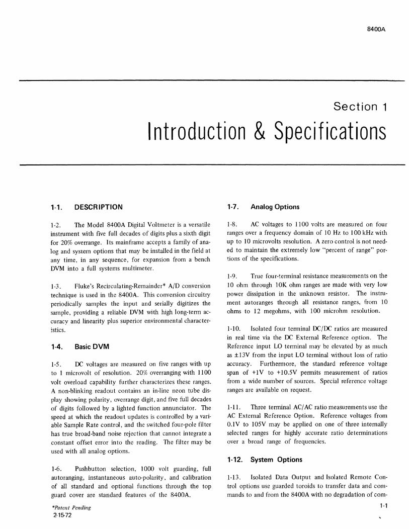
1-1. DESCRIPTION
1-2. The Model 8400A Digital Voltmeter is a versatile instrument with five full decades of digits plus a sixth digit for 20% overrange. Its mainframe accepts a family of analog and system options that may be installed in the field at any time, in any sequence, for expansion from a bench DVM into a full systems multimeter.
1-3. Fluke's Recirculating-Remainder* A/D conversion technique is used in the 8400A. This conversion circuitry periodically samples the input and serially digitizes the sample, providing a reliable DVM with high long-term accuracy and linearity plus superior environmental characteristics.
1-4. Basic DVM
1-5. OC voltages are measured on five ranges with up to 1 microvolt of resolution. 20% overranging with 1100 voit overload capability further characterizes these ranges. A non-blinking readout contains an in-line neon tube display showing polarity, overrange digit, and five full decades of digits followed by a lighted function annunciator. The speed at which the readout updates is controlled by a variable Sample Rate control, and the switched four-pole filter has true broad-band noise rejection that cannot integrate a constant offset error into the reading. The filter may be used with all analog options.
1-6. Pushbutton selection, 1000 volt guarding, full autoranging, instantaneous auto-polarity, and calibration of all standard and optional functions through the top guard cover are standard features of the 8400A.
*Patent Pending 2-15-72
1-7. Analog Options
1-8. AC voltages to 1100 volts are measured on four ranges over a frequency domain of 10 Hz to 100 kHz with up to 10 microvolts resolution. A zero control is not needed to maintain the extremely low "percent of range" portions of the specifications.
1-9. True four-terminal resistance measurements on the 10 ohm through lOK ohm ranges are made with very low power dissipation in the unknown resistor. The instrument autoranges through all resistance ranges, from 10 ohms to 12 megohms, with 100 microhm resolution.
1-10. Isolated four terminal OC/OC ratios are measured in real time via the OC External Reference option. The Reference input LO terminal may be elevated by as much as ±13V from the input LO terminal without loss of ratio accuracy. Furthermore, the standard reference voltage span of + 1 V to + 10.SV permits measurement of ratios from a wide number of sources. Special reference voltage ranges are available on request.
1-11. Three terminal AC/ AC ratio measurements use the AC External Reference Option. Reference voltages from 0.1 V to 105V may be applied on one of three internally selected ranges for highly accurate ratio determinations over a broad range of frequencies.
1-12. System Options
1-13. Isolated Data Output and Isolated Remote Control options use guarded toroids to transfer data and commands to and from the 8400A with no degradation of com-
1-1

8400A
mon-mode rejection specifications. ThP,se options are also DTLi'!TL compatible and are designed to permit multiplexing of several 8400A's on common sets of control and data output lines. Moreover, they are buffered to prevent interaction between the DVM and the acquisition/control devices.
log input prior to digitization of the data transferred. Five flags provide coniinuous measurement status information for the acquisition device.
1-14. External Triggering of the 8400A is accomplished via its Data Output Unit, and resulting data may be ac
quired fully in parallel BCD format or serially by character in multiples of four-bits. A single contr::il line enables automatic time delays that allow for full settling of the ana-
1-15. Remote Control is exerted by contact closures or logic levels. The 8400A's Control Command Storage feature permits the 8400A to latch on commands which may be later removed from inputs while the 8400A retains the commanded function and range in internal memory. Logical interlocks i>'.e a further important systems featu:,'.l of this option, because they preveri.t iiicornti~.tfoit,> :.:aiis,
1-16. SPECIFICATIONS
1-17. Mainframe
DC VOLTS
RANGES ........................... .
Resolution ......................... . Overrange ......................... .
±0. lV, ± 1V, ± 10V, ±100V, ± 1000V (automatic polarity selection)
±0.001% of range, (luV maximum on ±0.1V range) 20"/o, ±1100V maximum input on ±1000V range
Overload .......................... . ±1 lOOV DC or RMS (±1500V peak) may be continuously applied to any range without damage.
~CCU RACY (To 120";{, of range or± 1100V maximum input)
24 hours (23°C ±1°C)
± 10V, ± 100V, ± 1000V ranges. . ±.(0.002% of input+ 0.001% of range) ± 1 V range. . . . . . . . . . . . . . . . ±(0.003% of input + 0.002% of range) ±0.1 V range . . . . . . . . . . . . . . ±(0.003% of input + 0.005% of range)
90 days ±10V, ±100V, ±1000V ranges .. ±(0.004% of input+ 0.001% of range) {18°C to 28°C) ±1V range ............... ±(0.005% of input+ 0.002% of range)
±0.1 V range . . . . . . . . . . . . . . ±(0.005% of input + 0.005% of range)
1 year ±10V, ±100V, ±1000V ranges .. ±(0.01% of input+ 0.001% of range) (18°C to 28°C) ±1V range ............... ±(0.02% of input+ 0.002% of range)
±0. lV range. . . . . . . . . . . . . . ±(0.02% of input+ 0.005% of range)
Temperature Coefficients (0°C to 18°C and 28°C to 50°C)
±10V, ±100V, ±1000V ranges ........... ±(0.0003% of input+ 0.0001% of range)fC ± 1V range . . . . . . . . . . . . . . . . . . . . . . . . . ±(0.0004% of input+ 0.0002% of range)/°C ±0.lV range ........................ ±(0.0005% of input+ 0.0006% or range)fC
Input lmpedences ±10V range . . . . . . . . . . . . 10,000 megohms ± 1 V range . . . . . . . . . . . . . 1000 megohms shunted by less than 100 p.f. ±0.1V range............ 100 megohms ±100V, ±1000V range..... 10 megohms
Offset Curr>''lt at 23°C±1°C ............. . Less than ±5 pa. on any range Temperature Coett1cient .............. . Less than ± 1 pafC on any range
Zero Stability ....................... . Better than 5 uv for 90 days after a one hour warmup.
1-2 10/18/74

8400A
NOISE REJECTION
Normal Mode (filtered) .. Greater than 65 db @ 60 Hz (60 db @ 50 Hz) Maximum superimposed AC Voltage . . . . . . . . 50% of range peak AC, maximum Common Mode (with up to 1 K unbalance in either lead)
DC . . . . . . . . . . . . . . . . . Greater than 140 db AC to 60 Hz, Filter "in" ..
Filter "out" .. Greater than 140 db Greater than 100 db
NOTE: Common Mode Rejection specifications are maintained with any combination of options installed and are unaffected when grounded devices arc used in conjunction with the remote control or data output options.
RESPONSE TIME (from an input step change to a completed reading within 0.005% of the change when externally triggered.)
Filter "out".
Filter "in".
GENERAL
Digitizing Time
Sample Aperture Sample Rate ...
lc:s:. than 33 milliseconds less than 500 milliseconds
18 milliseconds 3 milliseconds
Smoothly variable from 13 per second to one per 4.5 seconds
via SAMPLE RATE control
NOTE: /' maximum sample rate of JO readings rer second is obtained when Model 8400A is externally triggered via Option
8400/1-0J.
Autorange Time
Filter .. - .....
Range Selection Function Selection.
Display ....... .
Filter "out" ... Filter "in"
50 milliseconds per range change
280 milliseconds per range change 4-pole active filter for use with DC volts, AC volts, and Re-
sistance measurements
Manual, Automatic Standard; Remote Optional Manual Standard, Remote Optional, Autoranges from S1 to KS1 In-line neon-tube display of polarity, overrange digit and 5 full
decades of digits. with automatic decimal placement plus an il-
luminated function annunciator.
Overload Limits (Maximum voltage that mciy be continuously applied without damage)
"Hi" to "Lo" ..... . "Lo" to "Guard" ...... _ ..
"Guard" to "Chassis'.' ...... .
Temperature Range, Operating
Humidity Range
Altitude Range,
Non-Operating . 0'0 c to +25°C ..
+25°C to +50°C .
Operating .. Non-Operating ... .
Shock and Vibration. . ...... _ ... .
Operating Power (including options).
Weight (including options) .
Size .......... . see Figure 1-1
Warm-up Time ..
1-18. Options
AC VOLTS
RANGES
Resolution Overrange
10/18/74
(Using Option 8400A-01)
See individual functions under "range", & "overload"
± 1 OOV DC or peak AC ±1000V DC or peak AC maximum Common Mode Voltage 0°C to +50°C
--4/C to +75°C Less than 80% relative humidity Less than 7(J'lo relative humidity
To 10,000 feet (3.048 kM) To 50,000 feet (15.25 kM) Meets requirements of MI L-T-21200H and Ml L-E-16400F
115/230 V AC ± 10%, 50 to 440 Hz, Less than 25W
Less than 20 pounds(9.08 kg)
31/i'' H x 17" W x 18" D (88.1 mm x 432 mm x 457 .4mm),
20 minutes to 1 year accuracy, 1 hour to full accuracy.
1V, 10V, 100V, 1000V
±0.001% of range, (10 uV maximum on 1V range)
20%, 1100V RMS maximum on 1000V range
1-3

8400A
Figure 1-1. MODEL 8400A OUTLINE D RAWING
Overload . . . . . . . . . . . . . . . . . . . . . . . . . . . . 11 OOV RMS may be continuously applied to any range without damage
Superimposed DC. . . . . . . . . . . . . . . . . . . . . . . ±1100V DC (Peak AC plus DC may not exceed ±1500V)
ACCURACY (To 120"/.i of range or 1100V maximum input)
0.001V to 500V, 50 Hz - 10 kHz. . ±(0.05% of input +0.005% of range) (90 days, 10 kHz - 50 kHz . . ±(0.1% of input +0.005% of range)
18°C to 28°C) 20 Hz - 50 Hz and
500V to 11 OOV, 90 days ( 18°C to 28°C)
50 kHz - 100 kHz . . . . . ±(0.5% of input +0.005% of range)* 10 Hz - 20 Hz . . . . . . . . ±(1.0% of input +0.0 1% of range) 50 Hz - 10 kHz ........ .. ±0.1% of input 10 kHz - 50 kHz .......... ±0.1 5% of input* 20 Hz - 50 Hz ... ... ..... . ±(0.5% of input +0.005% of range) 10 Hz - 20 Hz ........... . ±(1.0% of input +0.01% of range)
"NOTE: Input Volt - Hertz product should not ex ceed 2 x J07
Temperature Coefficients (0°C to 18°C and 28°C to 50°C)
10 Hz - 50 kHz ...... . .. . . ±(0.002% of input +0.0005% of range )f C 50 kHz - 100 kHz ......... ±(0.01 % of input +0.0005% of range) / °C
Input Impedance . . . . . .... .. . . .... . . .... 1.11 megohm, ±0.1%, shunted by less than 100 pf.
NOISE REJECTION Common Mode (with up to 100Q unbalance in either lead)
DC to 60 Hz . . . . . . . . . . . . . . . . . . . . . . . . Greater than 120 db
RESPONSE TIME (from an input step change to a completed reading within 0.05% of the change when externally triggered).
1-4
Filter "out". . . . . . . . . . . . . . . . . . . . . . . . . . . 100 milliseconds (input frequency greater than 400 Hz) Filter "in" . . . . . . . . . . . . . . . . . . . . . . . . . . . 500 milliseconds (any input frequency)
10/18/74
AC VOL TS (Using option 8400A-09)
RANGES .
For Measurement of DC-Coupled (AC+ DC) Voltages or AC Only.
1, 10, 100, 1000 VAC
Overrange
Resolution
Overload
Superimposed DC (AC only)
Max. Crest Factor
ACCURACY
20%, 1100V RMS maximum on 1000V range
0.001 % range
1100V RMS any range ( 1500V peak AC)
1100V DC (Peak AC plus DC may not exceed ±1500V)
7 at full-scale and increasing down scale per:
7X
V Range
V Input
AC+ DC AC ONLY
8400A
90 days,
(18°C to 28°C)
(0.001 V - 1100V(1 1)
D.C ..
50Hz-10kHz . 10kHz-30kHz (2)
30kHz-50kHz( 2)
20Hz-50Hz. .
10Hz-20Hz. .
50k Hz-100k Hz(2) .
100kHz-300kHz (21
;t(0.1% of input+ 0.03% of range)
±(0.1 % of input+ 0.03% of range)
±(0.2% of input+ 0.06% of range)
±(0.3% of input+ 0.12% of range)
±(0.5% of input+ 0.03% of range)
±(1.0% of input+ 0.06% of range)
±(1.0% of input+ 0.32% of range) ±(2.0% of input+ 0.52% of range)
±(0.1% of input+ 0.012% of range)
±(0.2% of input+ 0.04% of range)
±(0.3% of input+ 0.1 % of range)
±(0.5% of input+ 0.012% of range)
±( 1.0% of input+ 0.04% of range)
±( 1.0% of input+ 0.3% of range)
±(2.0% of input+ 0.5% of range)
(1) With inputs above 500 V multiply accuracy by f20oov + V inpu~ [ 2000V j
(2) Input volt x hertz, product should not exceed 2 x 1 o7.
Temperature Coefficients (0°C to 18°C and 28°C to 50°C)
DC and 10 Hz - 10 kHz (AC+ DC) . . ±(0.004% lnp. + 0.004% Range)
10 Hz - 10 kHz (AC only) ±(0.004% lnp. + 0.001% Range)
Input Impedance . 1 Megohm, shunted by less than 150 p.f.
NOISE REJECTION
Common Mode (with up to 10on unbalance in either lead)
DC to 60 Hz . . Greater than 120 db
RESPONSE TIME (to a reading within 0.1% of range when measuring step change inputs and using external trigger).
Filter "out"
Filter "in" .
100 milliseconds maximum (31
500 milliseconds maximum
(For readings less than 10% Range, double indicated times).
(3) Above 400 Hz for rated accuracies.
RESISTANCE (Using Option 8400A-02)
RANGES ................................... 10n, 10on, 10oon, 10,ooon, 100 Kn, 1000 Kn, 10,oooKn NOTE: Model 8400A will autorange through all resistance ranges.
Resolution .......................... . Overrange ........................... . Overload, 10n - 10,ooon ranges
1 OOKn - 10,000 Kn ranges .....
10/18/74
0.001% of range, (100 un maximum on 10 n range) 20%, 12 megohms maximum on 10,000K range 20V RMS (fused) Up to 250V RMS may be continuously applied without damage
1-5

8400A
ACCURACY (To 120% of range) 90 days, 100kr2 - 1000kQ ianges . . . . . . ±(0.01% of input +0.002~{, of iange} (18°C to 28°C) lOOQ -10,000Q ranges . . . . . . ±(0.01% of input +0.003~ of range)
1an range . . . . . . . . . . . . . . . ±(O.a1% of input +O.a1% of range)
1 O,OOOkQ range . . . . . . . . . . . ±(0.05% of input +O.Oa2% of range) Temperature Coefficients (0° to 18°C and 28° to 50°C)
lOOkQ, 1000kil ranges . . . . . . . . . . . . . . . . . ±(0.0007% of input +a.Oa01% of range)/°C 10,aOOkQ range. . . . . . . . . . . . . . . . . . . . . . ±(0.003% of input +o.oaa1% of range)/°C lOOQ - 10,0oan range . . . . . . . . . . . . . . . . . ±(O.Oa1% of input +O.Oa02% of range)/°C 10S1 range . . . . . . . . . . . . . . . . . . . . . . . . . ±(a.001% of input +O.OOa5% of range)/°C
CONFIGURATION . . . . . . . . . . . . . . . . . . . . . . . True 4-terminal through 10,000Q range and 2 terminal on the 100 Kil through 10,000 Kil ranges.
Current through R measured Range . . . . . . . . . . . . . . . . . . . . . . . . . . . lOQ, 10an, 1 ooan, 10,000Q,lOaKD lOOOKQ, 10,aoo Kil Current . . . . . . . . . . . . . . . . . . . . . . . . . . . 1a ma 1 ma lOOµa lOµa 1 µa
Maximum Lead Resistance (for less than a.001% of range effect on accuracy) 4 terminal mode, Current leads . . . . . . . . . . . lOQ in both leads on 1 OQ range and lOOQ on all other
ranges Voltage leads 1 KQ in either lead on all ranges.
2 terminal mode . . . . . . . . . . . . . . . . . . . . . Less than O.a01% of range lead resistance.
RESPONSE TIME (from an input step change to a completed reading within 0.01% of the change when externally triggered). Filter "out". . . . . . . . . . . . . . . . . . . . . . . . . . . Less than 33 milliseconds
Filter "in". . . . . . . . . . . . . . . . . . . . . . . . . . . . Less than 500 milliseconds
ISOLATED DC EXTERNAL REFERENCE (4 Terminal DC/DC Ratio using Ootion 840aA-05) NOTE: Mating connector is supplied.
REFERENCE INPUT Voltage Range. . . . . . . . . . . . . . . . . . . . . . . . . +1 V to +10.5V Input Resistance . . . . . . . . . . . . . . . . . . . . . . . 1 megohm ±0.1%
Isolation of Reference and Input Commons . . . . . . . . . . . . . . . . . . . . . V input + V common difference not to exceed± 13V on 1 OV NOTE: Fused to prevent damage. and lower ranges.
RANGES ............................. ±0.01:1, ±0.1:1, ±1:1, ±10:1, ±100:1
Resolution . . . . . . . . . . . . . . . . . . . . . . . . . . . ±a.Oa1% of Ratio range, (O.OOaaaa1: 1 maximum on ±O.al: 1 range) Overrange . . . . . . . . . . . . . . . . . . . . . . . . . . . 20%, 11a: 1 maximum input on 10a: 1 range Overload ............................. ±1100V DC or RMS (±1500V peak) may be continuously ap
plied to the numerator (input) terminals without damage. Reading vs. Ratio. . . . . . . . . . . . . . . . . . . . . . . 10 x Ratio
ACCURACY (To 120"/o of ratio ranqe) 90 days ± 1: 1, ± 10: 1, ± 100: 1 ranges ±(0.005% of Ratio +a.a02% x 1 av ref of range)
(18°C to 28°C) ±0.1: 1 range . . . . . . . . . . . . ±(O.a05% of Ratio +0.004% x 10V ref of range) ±O.al: 1 range. . . . . . . . . . . . ±(0.005% of Ratio +0.01% x 1 av ref of range)
NOTE: 24 hour and 1 year specifications available upon request.
Temperature Coefficients (a°C.to 18°C and 28°C to 50°C)
±1: 1,±10: 1,±lOa: 1 ranges ....•. ±(0.0003%ofratio+O.Oa01%x 10VIVrefofrange)/°C ±0.1: 1 range ............ ±(O.Oa04% of ratio +a.0002% x lOV IV ref of range)/°C ±0.01: 1 range ........... ±(O.OOa5% of ratio +0.0006% x lOV IV ref of range)/°C
NOISE REJECTION (At Reference Input) Normal Mode . . . . . . . . . . . . . . . . . . . . . . . . . 30 db @ 60 Hz Common Mode (with up to 1 K unbalance) ..... . 12a db with a + 10V Reference
1-6 10/18/74

84aaA
REFERENCE SETTLING TIME. . . . . . . . . . . . . . . 2 seconds
(To a.al% of range following a step change of reference voltage. Numerator response time same as "de volts").
AC EXTERNAL REFERENCE (3 Terminal AC/AC Ratio using Options 84aaA-a1 and 84aaA-06) NOTE: Mating connector is supplied.
REFERENCE INPUT Reference Ranges .... 1V, 1av, 10av (internal selection)
1 a% to 1 a5% of Reference Range Reference Voltage ..................... . Input Impedance ...................... . 1 megohm shunted by less than 10a pf.
RATIO RANGES Reference Range 1V ................. 1: 1, 10: 1, 100: 1, 10ao: 1
1 av. . . . . . . . . . . . . . . . . a.1 : 1. 1: 1, 1 a: 1. 1 aa: 1 1aav ................. a.al: 1, a.1: 1, 1: 1, 1a: 1
Resolution a.Oa1% of Ratio range, a.aaaaao1: 13aV RMS at Reference Input
1 maximum Overload ........................... . Reading vs. Ratio, 1 V Ref. Range ....... . 1 x Ratio
10V Ref. Range ....... . 1a x Ratio 10av Ref. Range ....... . 1aa x Ratio
ACCURACY (9a days at 18°C to 28°C and to 12a% of ratio range) 5a Hz - 10 kHz *
1: 1 Range and Reference and Input
* at the same frequency . . . . . . . . . . . . . . . . . ±(a.a5% of Ratio + a.aa5% x Ref Range/V ref of range)
NOTE: Specifications from JO Hz - 50 Hz and JO kHz - JOO kHz available on request.
Input and Reference not at the same frequency or not on the 1: 1 Range . . . . . . . . . . . ±(a.1 % of Ratio + a.aa5% x Ref. Range/V ref of range)
Temperature Coefficient (a"c to 18°C and 28°C to 5a°C).. . . . . . . . . . ±(a.aa4% of Ratio+ a.aa1% x Ref Range!Vref of range)
REFERENCE SETTLING TIME . . . . . . . . . . . . . . 2.5 seconds maximum.
(To O.a5% of range following a step change of reference voltage. Numerator response time same as "ac volts").
LSOLATED DATA OUTPUT (Using Option 84aaA-a3) NOTE: Two mating connectors are supplied.
Data Available. . . . . . . . . . . . . ....... . Coding ............................ . Logic Levels . . . . . . . . . . . ........... . Maximum Trigger Rate .................. .
Flags. . . . . . . . . . - . · · · · · · · · · · · · · · · · ·
Acquisition .......................... . Automatic Adaptive Timeouts ............. .
Digits, polarity, range, functions 8 4 2 1 BCD, digits and range 1 = +5V, a= av (Series 93a DTL with 6K pullup) 3a per second Digitizing, Remotely Controlled, Remotely Triggered, Ready, Overload Full parallel or serial by character in multiples of 4 bits Automatic delays to allow for settling time of all analog inputs are enabled via a single logic input line.
ISOLATED REMOTE CONTROL (Using Option 84aaA-a4) NOTE: Mating connector is supplied
Control Levels. . . . . . . . . . . . . . . . . . . . . . . . . a = function called, 1 = function inactive Logic Levels . . . . . . . . . . . . . . . . . . . . . . . . . a = Contact closure or av, 1 = open or +5 V Input Definition . . . . . . . . . . . . . . . . . . . . . . . Series 93a DTL Control Command Storage . . . . . . . . . . . . . . . Continuous or addressed remote control of instrument. Triggered
address control allows the 82aaA to "latch" to input commands. Following latch, the commands may be removed but the functions and ranges commanded will continue to be in effect until the next address trigger.
Interlocks. . . . . . . . . . . . . . . . . . . . . . . . . . . . Incompatible functions or simultaneous ranges cannot be
called.
10/18/74 1-7

8400A
AUTOMATIC
ADAPTIVE TIMEOUTS ENABLED
TIME -FOR TOTAL TIMES,
SEE TABLE
2-8
AUTOMATIC ADAPTIVE TIMEOUTS DISABLED
TIME -
EXT. TRIGGER (START BUSY FLAG)
1-8
ISOLATED DATA OUTPUT TIMING DIAGRAMS
FINAL SELF TRIGGER
BEGIN AUTO ZERO
END FINAL SYNC FLAG. END BUSY
FLAG(DATA READY)
\
~T TIME (10.5) \
END SAMPLE
END DIGITIZING
ASYNCHRONOUS DELAY(1.5 ms)
(3 ms)
P.O.S. DISABLE
END BUSY FLAG (DATA READY)
AUTORANGING DECISION
DELAY (4.5 ms)
FINAL APERATURE TIME (3 ms)
10/18/74

8400A
No Call Volts DC and autorange called
Flag Remotely controlled Flag in Data Output Unit
NOTE: Further Details available on request
PARALLEL REAR INPUT (Using Option 8400A-07)
,.uTE: Switchable Rear/Front Inputs available on special quote.
1-19. Accessories
• A90 Current Shunt • 80F-5 High Voltage Probe
• M00-260-610 18-inch Rack Slide
10/18/74
• • 80F-15 High Voltage Probe M00-280-610 24-inch Rack Slide
• • 80RF High Frequency Probe M03-203-601 Rack Ears
1-9/1-10

0 static awareness 0 A Message From
John Fluke M(g. Co., Inc.
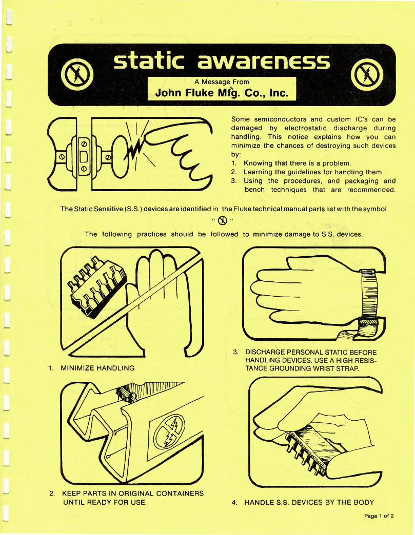
Some semiconductors and custom IC's can be damaged by electrostatic discharge during handling. This notice explains how you can minimize the chances of destroying such devices by: 1. Knowing that there is a problem. 2. Learning the guidelines for handling them. 3. Using the procedures, and packaging and
bench techniques that are recommended .
The Static Sensit ive (S.S.) devices are identified in the Fluke technical manual parts list with the symbol
"©" The following practices should be followed to minimize damage to S.S. devices.
1. MINIMIZE HANDLING
2. KEEP PARTS IN ORIGINAL CONTAINERS UNTIL READY FOR USE.
3. DISCHARGE PERSONAL STATIC BEFORE HANDLING DEVICES. USE A HIGH RESISTANCE GROUNDING WRIST STRAP.
4. HANDLE S.S. DEVICES BY THE BODY
Page 1 of 2
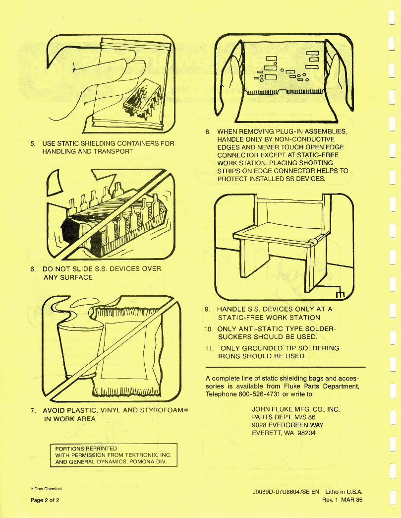
5. USE STATIC SHIELDING CONTAINERS FOR HANDLING AND TRANSPORT
6. DO NOT SLIDE S.S. DEVICES OVER ANY SURFACE
7. AVOID PLASTI C, VINYL AND STYROFOAM® IN WORK AREA
PORTIONS REPRINTED WITH PERMISSION FROM TEKTRONIX, INC. AND GENERAL DYNAMICS, POMONA DIV.
® Dow Chemical
Page 2 of 2
8. WHEN REMOVING PLUG-IN ASSEMBLIES, HANDLE ONLY BY NON-CONDUCTIVE EDGES AND NEVER TOUCH OPEN EDGE CONNECTOR EXCEPT AT STATIC-FREE WORK STATION. PLACING SHORTING STRIPS ON EDGE CONNECTOR HELPS TO PROTECT INSTALLED SS DEVICES.
9. HANDLE S.S. DEVICES ONLY AT A STATIC-FREE WORK STATION
10. ONLY ANTI-STATIC TYPE SOLDERSUCKERS SHOULD BE USED.
11. ONLY GROUNDED TIP SOLDERING IRONS SHOULD BE USED.
A complete line of static shielding bags and accessories is available from Fluke Parts Department, Telephone 800-526-4731 or write to:
JOHN FLUKE MFG. CO., INC. PARTS DEPT. MIS 86 9028 EVERGREEN WAY EVERETT, WA 98204
J0089D-07U8604/SE EN Litho in U.S.A. Rev. 1 MAR 86

8400A
Section 2
Operating Instructions
2-1. INTRODUCTION
2-2. This section contains operating instructions for the Model 8400A Digital Voltmeter If any problem is encountered in operating the instrument, contact the nearest John Fluke Sales Representative or write directly to the John Fluke Mfg. Co., Inc. Please include the instru· ment serial number when writing.
2-3. INSTALLATION
2-4. The 8400A is supplied with non-marring feet and tilt-down bail for bench or field use. A rack-mounting kit and rack-slide kits for installation of the iri. ument in a standard 19-inch rack are available. These accessories are described in Section 6 of the manual.
2-5. REPACKAGING FOR SHIPMENT
2-6. This instrument was packed and shipped in a foam-packed cardboard carton. If reshipment is required, use the original container or request a new container from the John Fluke Mfg. Co., ln1,;. Please include instrument model number with your request.
2-7. OPTIONS AND ACCESSORIES
2-8. Model 8400A options and accessories are listed in Table 2-1. They are fully described in Se,·t1nr ., of the manual.
2-9. INPUT POWER REQUIREMENTS
2-10. The 8400A operates on 115 or 230 volt, SO Hz to 440 Hz ac power. Before applying power to the instru-
10/18/74
Table 2-1. OPTIONS AND ACCESSORlfS ----,
Option No. Name -
8400A-01 AC Converter 8400A-02 Resistance Converter 8400A Data Output .AOOA-04 Remote Control 8400A-05 DC External Reference 8400A-06 AC Ev•crnal Reference 8400A-07 Rear ,.JUt 8400A-09 True RMS Converter
-01 required with -06 -01 and -09 cannot be Installed together -07 required with -05 or -06
Accessory No. Name
298265 Extender Assembly (Required for servicing pcb's)
M03-203-601 Rack Ears M00-260-610 18-inch Rack Slides M00-280-610 24-inch Rack Slides A90 Current Shunts SOF-5 High Voltage Probe 80F-15 High Voltage Probe 80RI= .____ High Frequency Probe
ment, no• the position of the 115/230 volt slide switch at the rear , Lhe instrument (Figure 2-1 ). ' witch does not indicate the desired operating voltag.. , . e it in the correct position.
WARNING!
Ensure that the instrument case is connected to a high quality earth ground, either through the polarized line plug or through a separately connected ground wire.
2-1

8400A
2-11 . OPERATING FEATURES 2-13. MEASUREMENT INSTRUCTIONS
2-12. The name and function of front and rear panel controls, terminals and indicators are shown in Figure 2-1.
2-14. Measurement instructions for basic DVM func-tions are given in Table 2-2.
REF. NO.
2
3
2-2
13 12
NAME
POWER Switch
Polarity Indicator
Readou t Tubes
2 3 4 5 6 7
11 10 9 8
14 15 16 17 18 19 20 21
22
FUNCTION
Controls application of input power.
Automatic indication of input polarity for de voltage: "+" for positive input voltages and "-"for negative input voltages.
Display DVM readout from left to r ight, with overrange digit displayed in left-most tube. All tubes display a decimal point, depending on range. Full overrange readout on each range would appear as follows:
RANGE READOUT
.1 .119999 1.19999
10 11.9999 100 119.999 1000 1199.99 10K 11999.9
Figure 2-1 . CONTROLS, TERMI NALS, AND INDICATORS (Sheet 1 of 3)
10/18/74

8400A
REF FUNCTION
NO. NAME
4 Function/Status Indicate instrument function and status as follows:
Annunciator Kn DVM operating in kilohm mode.
AC DVM operating in ac voltage mode.
DC DVM operating in de voltage mode.
n. DVM operating in ohms mode.
X REF DVM operating in External Reference mode.
FILT. Active 4-pole filter called for maximum noise rejection.
OVER DVM input is over the 20% overrange capability.
5 FUNCTION Select desired DVM operating mode: Switches EXT REF Enables substitution of isolated external reference voltage for internal
reference
FILT. Controls 4-pole active input filter to provide desired noise rejection. Fune-tional for de voltage, ac voltage, and resistance measurements.
VDC. Places DVM in de voltage mode with full-scale ranges of .1, 1, 10, 100, and 1000.
VAC. Places DVM in ac voltage mode with full-scale ranges of 1, 10, 100, and 1000.
n. Places DVM in ohms mode with full-scale ranges of 10, 100, 1000, and 10K if available range is called; otherwise, DVM autofunctions to Kn.
Kn Places DVM in kilohms mode with full-scale ranges of 100, 1000 and 10K if available range is called; otherwise, DVM autofunctions to n.
REMOTE Places DVM in remote mode, enabling DVM function and range to be con-trolled remotely via the Remote Control Unit.
6 INPUT HI, LO input connections for de and ac voltage measurement. Terminals
7 n SOURCE Current source for all resistance measurements. Terminals
8 GD (Guard) Connects to internal guard chassis. When properly connected externally, provides maximum Terminal common mode rejection.
9 DC ZERO Adjusted for .000000 ± 1 with VDC, Filter, and .1 Range called and INPUT terminals Control shorted.
10 AUTO RANGE Places DVM in autorange mode, providing automatic ranging for each function and its range Switch complement.
11 Manual RANGE Enable manual selection of DVM range. Not calling a range or incorrect range selection au-tomatically places DVM in autorange mode.
12 Sample Rate Visual indication of sample rate. Indicator
13 SAMPLE RATE Permits variation of DVM sample rate from 13 readings per second to 1 reading per 4.5 Control seconds. In EXT position (fully counterclockwise). sample rate control is transferred to re-
mote control point via the Data Output Unit. If the Data Output option is not installed and the control is turned to EXT, the DVM will read out and display from its internal storage circuitry indefinitely, with readout corresponding to value of last measurement sample.
Figure 2-1. CONTROLS, TERMINALS, AND INDICATORS (Sheet 2 of 3)
2-3
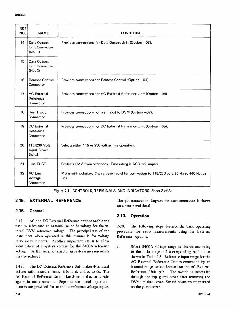
8400A
NO. NAME FUNCTION
14 Data Output Provides connections for Data Output Unit (Option -03). Unit Connector (No. 1)
15 Data Output Unit Connector (No. 2)
16 Remote Control Provides connections for Remote Control (Option -04). Connector
17 AC External Provides connections for AC External Reference Unit (Option -06). Reference Connector
18 Rear Input Provides connections for rear input to DVM (Option -07). Connector
19 DC External Provides connections for DC External Reference Unit (Option -05). Reference Connector
20 115/230 Volt Selects either 115 or 230 volt ac line operation. Input Power Switch
21 Line FUSE Protects DVM from overloads. Fuse rating is AGC 1/2 ampere.
22 AC Line Mates with polarized 3-wire power cord for connection to 115/230 volt, 50 Hz to 440 Hz, ac Voltage line. Connector
Figure 2-1. CONTROLS, TERMINALS, AND INDICATORS (Sheet 3 of 3)
~15. EXTERNAL REFERENCE
2-16. General
2-1 7. AC and DC External Reference options enable the user to substitute an external ac or de voltage for the internal DVM reference voltage. The principal use of the instrument when operated in this manner is for voltage ratio measurements. Another important use is to allow substitution of a system voltage for the 8400A reference voltage. By this means, variables in systems measurements may be reduced.
2-18. The DC External Reference Unit makes 4-terminal voltage ratio measurements: ±de to de and ac to de. The AC External Reference Unit makes 3-terminal ac to ac voltage ratio measurements. Separate rear panel input connectors are provided for ac and de reference voltage inputs.
2-4
The pin connection diagram for each connector is shown on a rear panel decal.
2-19. Operation
2-20. The following steps describe the basic operating procedure for ratio measurements using the External Reference options:
a. Select 8400A voltage range as desired according to the ratio range and corresponding readout, as shown in Table 2-3. Reference input range for the AC External Reference Unit is controlled by an internal range switch located on the AC External Reference Unit pcb. The switch is accessible through the top guard cover after removing the DVM top dust cover. Switch positions are marked on the guard cover.
10/18/74
8400A
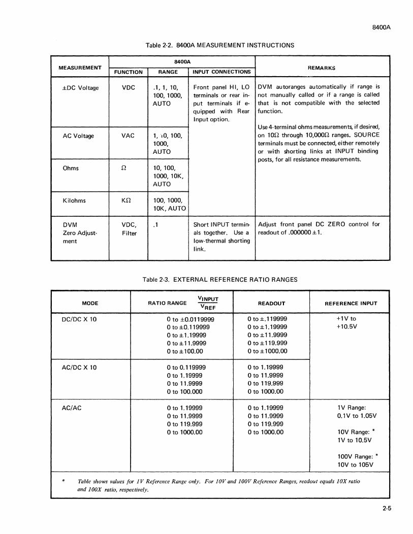
Table 2-2. 8400A MEASUREMENT INSTRUCTIONS
8400A MEASUREMENT
FUNCTION RANGE INPUT CONNECTIONS REMARKS
±DC Voltage VDC .1, 1, 10, Front panel HI, LO DVM autoranges automatically if range is
100, 1000, terminals or rear in- not manually called or if a range is called
AUTO put terminals if e- that is not compatible with the selected
quipped with Rear function. Input option.
Use 4-terminal ohms measurements, if desired,
AC Voltage VAC 1, 10, 100, on 10Q through 10,000Q ranges. SOURCE
1000, terminals must be connected, either remotely
AUTO or with shorting links at INPUT binding posts, for all resistance measurements.
Ohms n 10, 100, 1000, 10K, AUTO
Kil ohms Kil 100, 1000, 10K, AUTO
DVM VDC, .1 Short INPUT termin- Adjust front panel DC ZERO control for
Zero Adjust- Filter als together. Use a readout of .000000±1.
ment low-thermal shorting link.
Table 2-3. EXTERNAL REFERENCE RATIO RANGES
RATIO RANGE V1NPUT
MODE --- READOUT REFERENCE INPUT VREF
DC/DC X 10 0 to ±0.0119999 0 to ±.119999 +1V to
0 to ±0.119999 0 to ± 1. 19999 +10.5V
0 to ± 1 . 19999 Oto± 11.9999 0 to ± 11.9999 0to±119.999 0to±100.00 0 to±1000.00
AC/DC X 10 0 to 0.119999 Oto 1.19999 0 to 1.19999 0 to 11.9999 Oto 11.9999 0 to 119.999 0 to 100.000 0 to 1000.00
AC/AC 0 to 1.19999 0 to 1.19999 1V Range:
0 to 11.9999 0 to 11.9999 0.1V to 1.05V 0 to 119.999 0 to 119.999 0 to 1000.00 0 to 1000.00 10V Range: *
1V to 10.5V
100V Range: * 10V to 105V
* Table shows values for 1 V Reference Range only. For JOV and JOOV Reference Ranges, readout equals JOX ratio
and 1 OOX ratio, respectively.
2-5

8400A
EXTERNAL REFERENCE UNIT REFERENCE VOLTAGE ii~PUT
oc
AC
+lv to+lO.Sv
lv, lOv and lOOv ranges. (Maximum input: 130v nns.)
b. Connect reference voltage to rear input terminals.
c.
d.
Press EXT REF switch on the front panel.
Press VOC switch if de-to-de voltage ratios are to be measured or VAC switch if ac-to-dc/ac ratios are to be measured.
2-21. Installation, theory of operation, and maintenance instructions for the External Reference options are covered in Section 6 of the manual.
2-22. REMOTE CONTROL UNIT
2-23. General
2-24. The Remote Control Unit (RCU) enables the 8400A to be programmed or controlled remotely. RCU inputs are designed to interface directly with DTL/TTL logic. Control by discrete transistors or contact switches is also possible. Operating power for the RCU must be supplied from an external +5 volt source having a current capability of at least 150 milliamperes. Power may be obtained from the Data Output Unit option if the DVM is so equipped.
2-25. The RCU provides the capability of controlling all DVM functions and ranges, with logic interlocking provided so that incompatible functions or simultaneous
ranges cannot be called. Acceptable combinations are shown in Table 2-4.
2-26. RCU Command Triggering
2-27. The RCU has two operating modes which control entry of external commands into the unit: continuous command mode and triggered command mode.
2-28. In continuous command mode, the RCU requires no external triggering. The instrument always reflects present state of command inputs in continuous mode. To achieve this mode of operation, hold pin 35 (Auto Command Entry Defeat) and pin 33 (External Command Entry) at logical "l" (+5v) or open.
2-29. In triggered command mode, the RCU will only respond to programming inputs after application of an external trigger. It will memorize input commands within 10 microseconds of trigger application. Following the storage operation, programming inputs may be changed or removed without affecting stored information. To achieve this mode of operation, hold pin 35 (Auto Command Entry Defeat) low by application of logical "O" or contact closure and apply the external trigger to pin 33 (External Command Entry). RCU connector location is shown in Figure 2-1. Pin assignments are given in Table 2-5. Trigger requirements (External Command Entry) are given in Figure 2-2.
2-30. Operation
2-31. To place DVM in remote operation, proceed as follows:
a. Press REMOTE FUNCTION switch to transfer control of DVM function and range to the remote control point.
Table 2-4. REMOTE CONTROL UNIT LOGIC INTERLOCKING
FUNCTION RANGE CALLED FILTER RATIO
CALLED .1 1 10 100 1000 10K NONE
voe . 1 1 10 100 1000 AUTO AUTO YES YES
VAC AUTO 1 10 100 1000 AUTO AUTO YES YES
n AUTO AUTO 10 100 1000 10K AUTO YES NO
Kn AUTO AUTO AUTO 100 1000 10K AUTO YES NO
NOTE: I. If function and range are not called, D VM goes to VDC mode and autoranges (providing REMOTE button is pressed).
2. When ranges are selected manually, D VM will auto/unction between .Q and Kil if the selected range does not agree with the called function.
2-6

Table 2-6. REMOTE CONTROL UNIT PIN ASSIGNMENTS
FUNCTION PIN FUNCTION PIN
NO. NO.
Common *2 VAC 17
Common *4 KD 19
Common *6 IT 23 1 Range 7 1RaiiQe 25
Common *8 100 Range 27
+5V Input **9 External Reference 29 1000 Range 11 Fiite;: 31
10K Range 13 External Command Entry ***33 10 Range 15 Auto Command Defeat ***35
b.
Spare Pins: 1, 3, 5, 10, 12, 14, 16, 18, 20, 22, 24 26, 28,30,32,34,3f.
LOGIC LEVELS
LOGIC 1 = +5V OR OPEN
(INPUT DEVICE MUST BE
ABLE TO SOURCE 40µAMP
AT 2.6V)
LOGIC 0 = OV OR CONTACT CLOSURE
(INPUT DEVICE MUST BE
ABLE TO SINK AT 1.6 MA AT OV)
TRUTH TABLE
1 ·FUNCTION NOT CALLED
0 = FUNCTION CALLED
NOTES:
*
**
***
Isolated from Input "LO" and chassis
+ 5 V Input: Maximum current requirement = I 50 milliamperes. (A Pai/able from DOU)
Used only in Control Command Storage mode of operation. No connections are required when RCU is controlled with continuously applied commands.
If remote control of DVM sample rate is desired, turn SAMPLE RATE control to its extreme CCW position (EXT). In EXT position, the internal sample rate oscillator is disabled and the DVM sample command is applied via the Data Output Unit. If the Data Output Unit is not installed and the control is turned to EXT, the DVM will readout and display from analog storage indefinitely. !The readout will correspond to the value of the last measurement.
10/18/74
8400A
A. POSITIVl TRIGGER
POSITIVF fRIGGER •5V
USED TO ~NTER .n.. EXTERNAi COMMAND ov:J r-- 1 J.lSE.C MINIMUM
LOGIC "1 "I 16 J!.SEC MINIMUM ~ DURATION FROM
RCUINPUICONTROL i I EDGEOFTRIGGER
LINE FOR FUNCTION ~ TO BE PROGRAMMED l
LOGIC "O"
B. INVER l ID TRIGGER
LOGIC "1" TO LOGIC "O'· TRANSi TION SHOULD OCCUR NO LATER THAN SIMULTANEOUSLY W•TH LEADING EDGE OF TRIGGER
INVERTED TRIGGER +5 V
USED TO ENTER -:::::J ~MINIMUM EXTERNALCOMMAND ~ ~,......,~~
OV 'M 16J.1SEC MINIMUM : DURATION FROM
LOGIC '1" I TRAILING EDGE I RCU INPUT CONTROL ~1 OF TRIGGER LINE FOR FUNCTION : TO BE PROGRAMMED
LOGIC "O" LOGIC '1 TO LOGIC 'O TRANSITION SHOULD OCCUR NO UHER THAN SIMULTANEOUSLY WITH TRAILING EDGE OF TRIGGER
C. NOTES
TRIGGER WAVEFORM RESTRICTIONS: PULSE. LOGIC LEVEL, OR SINE WAVE INPUTS WORK EQUALLY WELL
TRIGGER RISETIME RESTRICTIONS: OC TRIGGERED AT 1.5V ("0" TO "1" TRAN· SITION), TRIGGER CIRCUIT ARMED AT 0.BV ("1" TO "O" TRAN SITION).
c.
Figure 2-2. REMOTE CONTROL UNIT TRIGGER REQUIREMENTS (EXTERNAL COMMAND ENTRY)
Command a function or range via a contact closure or a zero volt logic level between the appropriate pin and common. For example, to program lOk ohm, filtered operation, command pins 13, 23, and 31 via contact closure or zero volts to pin 2, 4, or 6 (commons).
2-32. Installation, theory of operation, and maintenance instructions for the Remote Control Unit are covered in Section 6 of the manual.
2-33. DATA OUTPUT UNIT
2-34. General
2-35. DOU access is by means of two card-edge connectors located at the rear of the instrument (Figure 2-1 ). Data may be acquired fully in parallel BCD format or serially by character in multiples of four-bits. The Programmed OneShot (POS) line enables automatic time delays that allow for full settling of analog input circuitry prior to data transfer.
2-7

8400A
2-36. The DOU is self powered and provides +SV {150 milliamperes maximum) output for operation of the Remote Control Unit {Option -04) or other logic circuitry. DOU truth tables and logic levels are given in Table 2-6. Functional pin connections for the DOU are given in Table 2-7.
2-37. Control Signals
2-38. DOU control inputs consist of External Trigger, External Trigger Inhibit, and Programmed One-Shot. The External Trigger may be a positive or negative going signal, as shown in Figure 2-3. The External Trigger Inhibit input must be a logical "O" to inhibit and a logical "l" to enable. The Programmed One-Shot input must be a logical "l" for fast operation (timeouts defeated) and a logical "O" for normal operation {programmed timeouts).
NEGATIVE
TRIGGER +5V :u (Trailing edgel OV -
POSITIVE +SV -
TRIGGER OV (Leading edge)
20us _.l_I;:' Minimum
1 us
WAVEFORM RESTRICTIONS: None. DOU will operate equally well with pulse, logic level, or even sine wave in-puts.
RISETIME RESTRICTIONS: DC triggered at 1.5V ("0" to "1" transition).
Figure 2·3. DATA OUTPUT UNIT TRIGGER REQUIREMENTS
2-39. The Sample Sync signal corresponds in timing to the DVM sample periods occurring in each measurement period, as shown in Figure 24. During the time the DVM is busy processing a request for data, the time of occurrence of the second or final sample period is subject to a number of delays, depending on DVM operating mode, autoranging delays, etc. The purpose of the Sample Sync signal is to inform the DVM input signal acquisition device (scanner) when the final sample is taken by the DVM. This information is useful when the DVM is used in a scanning system, where it is desirable that inputs be changed at the earliest possible time without altering the previous sample.
2-40. Programmed One-Shot
241. The response of the 8400A Data Output Unit to a data request consists of a function-dependent series of delays. When enabled, the Programmed One-Shot circuit in the DOU automatically sequences the delay series to provide data within specified accuracy in the minimum possi-
2-8
I J:VT n TRIGG~ ·'-------.s
1 :-1.5ms
I I 4.5ms+ TOTAL I I I ~TIME OUT -c I
I I II CHART FIGURE 2-5 I I I , I I
BUSY __J _J18 msL -!18 msJ._ I 1 I I
SAMPLE I :FIRST FINAL I I SYNC I 1sYNc SYNC 1 1
h-l f~ SAMPL9E ___ --'_.I j- 3 ms j ,___::j ~s u u
Figure 2-4. SAMPLE SYNC. SIGNAL TIMING (AUTO-MATIC ADAPTIVE TIMEOUTS ENABLED).
ble time. If settling time is not a problem in specific applications, convenience is enhanced by provision for defeat of the POS, allowing sample rates as high as 30 per second. Application of +Sv logic level or open circuit to pin 2 defeats the POS {Fast Sample); application of logic zero or contact closure to pin 2 enables thePOS (Normal Sample). Figure 2-5 illustrates the timing of the events that occur
\END "AST \ SAM'LE
EXT TRIGGER (START BUSY FLAGI
\
ND"RSl GITIZING
END FIRST
SYNC FLAG
END DIGITIZING
POS DISABLE
DELAY 18m•I
!DATA READYI
FINAL APERATURE
TlME IJm•I
Figure 2-5. 8400A MEASUREMENT CYCLE TIMING DIAGRAM.
10/18/74
8400A
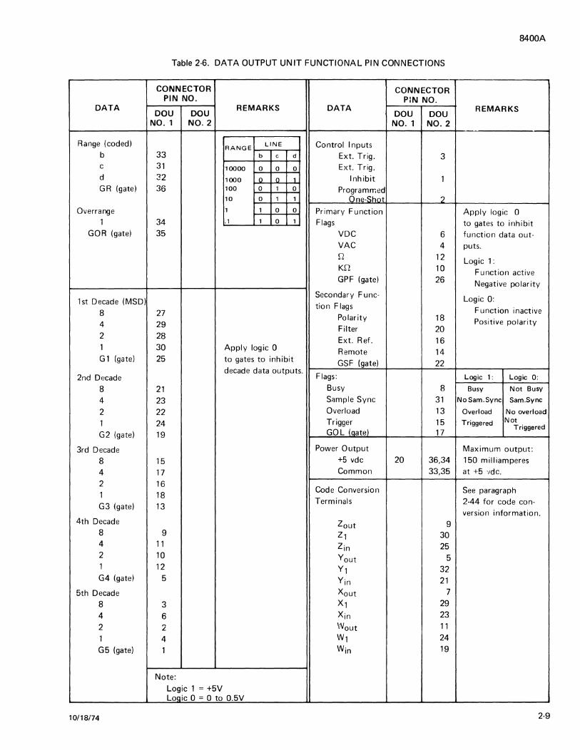
Table 2-6. DATA OUTPUT UNIT FUNCTIONAL PIN CONNECTIONS
CONNECTOR CONNECTOR PIN NO. PIN NO.
DATA DOU DOU
REMARKS DATA DOU
REMARKS DOU
NO. 1 NO. 2 NO. 1 N0.2
Range (coded) RANGE
LINE Control Inputs b 33 b c d Ext. Trig. 3 c 31 10000 0 0 0 Ext. Trig. d 32 1000 __Q_ __Q_ _j_ Inhibit 1 GR (gate) 36 100 0 1 0 Programrr.ed
10 0 1 1 0 ne.:S_l)Q_t _2
Overrange 1 1 0 0 Primary Function Apply logic 0 1 34 .1 1 0 1 Flags to gates to inhibit
GOR (gate) 35 voe 6 function data out-VAC 4 puts. D 12 Logic 1: KD 10 Function active GPF (gate) 26 Negative polarity
1st Decade (MSD) Secondary F unc- Logic 0:
8 27 tion Flags Function inactive
Polarity 18 Positive polarity 4 29 Filter 20 2 28 Ext. Ref. 16 1 30 Apply logic 0 Remote 14 G1 (gate) 25 to gates to inhibit GSF (gate) 22
2nd Decade decade data outputs.
Flags: Logic 1: Logic 0:
8 21 Busy 8 Busy Not Busy
4 23 S;imple Sync 31 No Sam.Sync Sam.Sync
2 22 Overload 13 Overload No overload
1 24 Trigger 15 Triggered Not
GO L J.9.ataj_ 17 Triggered
G2 (gate) 19
3rd Decade Power Output Maximum output:
8 15 +5 vdc 20 36,34 150 milliamperes
4 17 Common 33,35 at +5 ·1dc.
2 16 Code Conversion See paragraph
1 18 G3 (gate) 13
Terminals 2-44 for code con-version information.
4th Decade Zaut 9 8 9 z, 30 4 11 Zin 25 2 10 Yout 5 1 12 Y1 32 G4 (gate) 5 Yin 21
5th Decade Xout 7
8 3 x, 29
4 6 Xin 23
2 2 Waut 11
1 4 w, 24
G5 (gate) 1 Win 19
Note:
Logic 1 = +5V LQY.ic 0 = 0 to 0.5V
10/18/74 2-9

8400A
during the busy flag. The total busy flag time when the automatic adaptive timeouts are enabled, is given in Tabie
2-7.
2-42. Code Conversion
2-43. The 84-2-1 BCD code (standard) used in the 8400A may be converted to some other code, using the convenient code conversion terminals provided at the output connector on DOU No. 2. To convert to another code
remove the jumpers and connect the code conversion network, as shown in Figure 2-6. Usually only two integrated circuits are required in the network vs. about twelve for parallel conversion at the outputs, so a considerable saving may be realized. Detailed information regarding code conversion is available from the factory.
2-44. Figure 2-7 contains comprehensive timing diagrams for measuring both switched and continuously applied inputs when the D.O.U.'s automatic adaptive timeouts are not enabled.
2-45. OUTPUT FLAGS
2-46. Besides the Busy Flag (Data Not Ready), there is also a Sample Sync Flag. This flag goes to logic "l" when
the DVM starts sampling the input signal (aperture window opening). By using the Sample Sync Flag (negative transisition - leading edge), plus an external 3 millisecond, one-
8400A P20 PIN
DOU NO. 2 r---------------.
WouT I
XouT
YouT
ZouT
H3 H4 H5
NO.
11
7
5
9
Table 2-7. TOTAL BUSY FLAG TIME OUT (Autornatic Adaptive Timeouts Enabled)
FUNCTION TOTAL TIME MS
RANGE FILTER OUT FILTER IN
VDC-10, 100, 54 ±3 523 ±42 1000
VDC-0.1, 1 .0 123 ±10 523 ±42
VAC - all ranges 123 ±10 523 ±42
n - all ranges 123 ±10 523 ±42
kQ - all ranges 73 ±6 523 ±42
Autorange - per Add 50 Add 280 range change
shot delay, total data acquisition time can be decreased when using input scanners or a changing input signal which require long settling times. This will take advantage of the fact that the aperture window is only open for 3 milli
seconds allowing the input signal to be changed and to be settled before the next sample aperture occurs. When the Automatic Timeouts are enabled, the final sample sync flag must be used instead of the initial or intermediate sync
flags. See Figure 24 for timing of the sample sync flag.
2-4 7. The trigger flag indicates if the DVM is being triggered internally or externally. Other flags are the over-
H6 ...._-<">_z_1 N ______ __;~
25 >--------------1
CODE
CONVERSION
NETWORK
(CUSTOMER
SUPPLIED
USUALLY ONLY
2 IC'S ARE
REQUIRED)
2-10
lST
DECADE
CODE
YIN
--------------~
21
23
19
24
29
32 >--------------~-l
30 >------------------1 To convert from 1-2-4-8 BCD code to some other code, (1)
remove jumpers HJ through H6 (located at rear of DOU pcb
No. 2) and (2) connect code conversion network as shown;
otherwise, leave as is.
Figure 2-6. CODE CONVERSION
10/18/74

1. WITH PROGRAMMED FUNCTION AND/ OR RANGE CHANGE -AUTORANGING NOT ALLOWED.
PROGRAM 8400A TO NEW FUNCTION
CHANGE INPUT
TRIGGER 8400A
BUSY FLAG
MILLISECONDS
---- BUSY
0 B+25 8+58
B = BUFFER SETTLING TIME FROM TABLE D
25 =TIME TO SWITCH 8400A INTERNAL RELAYS
a. SIMULTANEOUSLY CHANGE INPUT AND PROGRAM FROM A FORMER FUNCTION TO A NEW ONE WHEN FORMER INPUT DOES NOT CAUSE OVERLOAD CONDITION FOR NEW FUNCTION, OR NEW INPUT WOULD NOT CAUSE OVERLOAD CONDITION FOR OLD FUNCTION. (SEE SPECIFICATIONS ON DATA SHEET).
PROGRAM 8400A
TO AC/DC VOL TS
CHANGE INPUT TO VOLTS
!.___Jr---------~
I I
TRIGGER 8400A I I
BUSY FLAG I I I
MILLISECONDS I I I I I
0 I A+ 25 I A+B+58 25 A+ B + 25
B = BUFFER SETTLING TIME FROM TABLE D
A = TIME TO SWITCH INPUT
25 =TIME TO SWITCH 8400A INTERNAL RELAYS
b. PROGRAM 8400A TO AC OR DC VOL TS FROM ilOR Kil, THEN APPLY A VOLTAGE INPUT GREATER THAN SPECIFIED il OR Kil "OVERLOAD" INPUT. (SEE SPECIFI CATIONS ON DATA SHEET)
PROGRAM 8400A TOilORKil __J
I CHANGE INPUT 1
8400A
TO il OR Kil .------------,
TRIGGER 8400A
BUSY FLAG
MILLISECONDS
------ - BUSY ___ ___,
0 I A+ B + 25
A A+8+58
B = BUFFER SETTLING TIME FROM TABLE D
A = TIME TO SWITCH INPUT
25 =TIME TO SWITCH 8400A INTERNAL RELAYS
c. PROGRAM 8400A TO il OR Kil FROM AC OR DC VOL TS WHEN INPUT VOLTAGE IS GREATER THAN SPECIFIED OVERLOAD FOR il OR Kil INPUTS. (SEE SPECIFICATIONS ON DATA SHEET).
2. WITH PROGRAMMED RANGE CHANGE BUT NO FUNCTION CHANGE.
PROGRAM 8400A TO NEW RANGE
CHANGE INPUT
TRIGGER 8400A
READY FLAG
MILLISECONDS
BUSY
0 B + 25 B + 58
B = BUFFER SETTLING TIME FROM TABLE D
25 =TIME TO SWITCH 8400A INTERNAL RELAYS
TABLED
BUFFER SETTLING TIME TABLE
BUFFER SETTLING TIME IN MILLISECONDS
FUNCTION RANGE FILTER FILTER "OUT" "IN"
DCV .lV 100 500 1,10,100 33 500 1000 33 500
ACV ALL 33 500
il 10 100 500 100,1000 33 500 10,000 33 500
Kil 100 33 500 1000,1000 33 500
Figure 2-7. SINGLE READING TIMING REQUIREMENTS WHEN D.0.U.'S AUTOMATIC ADAPTIVE TIMEOUTS ARE NOT ENABLED.
10/18/74 2-11

8400A
load, Volts DC, Volts AC, Ohms, Kilohms, Polarity, Filter, External Reference and Remuie Flags which are selfexplanatory. Refer to Table 2-7 for pin connections and level information.
2-48. Completely Parallel Data Acquisition
2-49. For completely parallel data acquisition, perform the following steps:
a. Determine the BCD code to be used and wire accordingly (see paragraph 2-42 for code conversion information).
b.
c.
d.
e.
NOTE!
8-4-2-1 BCD is supplied in standard 8400A.
Acquire full digits data by connection to the decade outputs. Leave inhibit lines associated with each decade open.
Acquire function, range, overrange and polarity data as desired. Leave associated inhibit lines open.
If data output is to be applied to a printer, the foregoing data could be grouped for presentation in several printer columns, with each column weighted as desired.
Acquire busy, overload, and trigger flags for use as desired.
2-50. Serial Character, Parallel Bit Acquisition
2-51 For serial character, parallel bit acquisition, per-form the following steps:
a. Determine the BCD code to be used and wire accordingly (see paragraph 2-42 for code conversion information).
b. Connect function, range, polarity, and digit outputs in parallel, as shown in Figure 2-8 or in groups of 8, 12, 16 bits, etc., as desired.
c. User supplied clock controls inhibit lines to determine the sequence of character acquisition. Data is transferred to the output lines when the associated inhibit lines are high. Truth tables and acquisition format are also shown in Figure 2-8.
2-52. Minimum Lines Acquisition
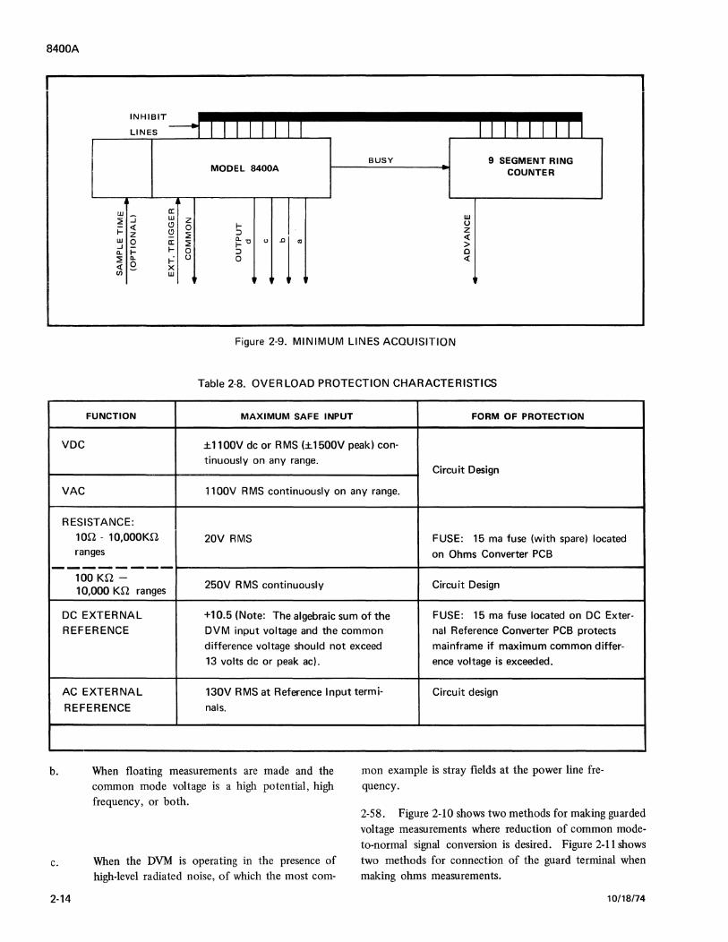
2-53. Minimum lines acquisition is a practical application of serial character, parallel bit acquisition, in which a user-supplied clock is placed near the 8400A to sequentially control the inhibit lines. Proceed as follows:
2-12
a.
b.
c.
d.
Place a customer fabricated 9-segment ring count-
ure 2-9.
Trigger the 8400A. (The Sample Time line may be programmed via interface or it may be hardwired).
When data is ready, transition of the 8400A BUSY signal will start the ring counter. A synchronizing pulse, sent from the ring counter's advance line, will allow the acquisition device to recognize the character being acquired on the four output lines.
An OVERLOAD line is available to serve as an a-larm or priority interrupt.
2-54. Installation, theory of operation, and maintenance instructions for the Data Output Unit are covered in Section 6 of the manual.
2-55. OPERATING NOTES
2-56. Overload Protection
2-57. The 8400A is protected against overload in each function and on all ranges. Table 2-8 lists the maximum voltages that may safely be applied to the DVM on all ranges.
2-58. Guarded Measurements
2-59. The 8400A employs a system of shields and guards that function (when properly connected) to minimize common mode-to-normal mode signal conversion and induced noise, thereby providing the user with a versatile systems DVM capable of fully-floating measurements without significant degradation of accuracy.
2-60. Non-floating measurements will likely be the usual case. Under these conditions, it is satisfactory to strap the front panel guard (GD) terminal to the LO input terminal using the shorting link provided.
CAUTION!
If guarded measurement is not needed, the DVM guard terminal should be connected to the IN PUT LO terminal at the front panel to preclude possible damage to the instrument.
2-61. In general, guarded voltage and resistance measurements will be necessary under the following conditions:
a. When long signal leads are used and signal source impedance is high.
10/18/74

::.:: u 0 ...J u
10/18/74
WIRING EXAMPLE
~ ? ~ ) 0 "'""Inhibit GS 1d 1c 1b 1a
~ ) ) ) > Inhibit G4 2d 2c 2b 2a
.... > > > ....,Inhibit G3 3d 3c 3b 3a
• > ) > Inhibit 4d 4c 4b 4a G2
.... ) ) ) )
...-Inhibit G1 Sd Sc Sb Sa
• > Inhibit GOA
~ :::-
r---t'·-.... v-
• < < Inhibit c b a
GR ..... _ ....
~ > ) ) ) 7.,hibit voe l\IA~ REF K!1 GPF
~ ) ) > "'"" Inhibit POL GSF
Fill REF ~EM
~ .. ~ ~ .. ~
\ D C B A I v OUTPUT LINES
STH DECADE
4TH DECADE
3RD DECADE
2ND
DECADE
1ST DECADE
>4----
OVER RANGE
RANGE
PRIMARY FUNCTION
SECONDARY FUNCTION
ACQUISITION FORMAT
BIT 0 1 2 3 4 s
d 0 1 0 1 0 1
c 0 0 1 1 0 0
b 0 0 0 0 1 1
a 0 0 0 0 0 0
RANGE
10K
BIT 0 1 1000
d 0 1 100
c 0 0 10
b 0 0 1
a 0 0 .1
FUNCTION
voe
VAC
n K!1
FUNCTION
POL
FILT
REF
REM
6 7 8
0 1 0
1 1 0
1 1 0
0 0 1
BIT
a b
0 0
0 0
0 1
0 1
1 0
0
BIT
a b
0 0
0 0
0
0
BIT
a b
0 0
0 0
0
0
Figure 2-8. WIRING EXAMPLE, ACQUISITION FORMAT, AND TRUTH TABLES FOR SERIAL CHARACTER, PARALLEL BIT ACQUISITION
8400A
9
1
0
0
1
c d
0 0
1 0
0 0
1 0
0 0
0
c d
0
0
0 0
0 0
c d
0
0
0 0
0 0
2-13
8400A
INHIBIT
LINES
w_ ::;;; ...J
~ <( 2
w Q ...J IL I-::;;; IL
<( 0 en
FUNCTION
voe
VAC
RESISTANCE:
1on - 10.oooKn ranges
a: w Cl
2 0
Q ::;;; a: ::;;; I- 0 i-..: 0 x w
MODEL 8400A
I-:::> i: 'C u
:::> 0
BUSY
l w 0 2 <(
> 0 <(
9 SEGMENT RING COUNTER
Figure 2-9. MINIMUM LINES ACQUISITION
Table 2-8. OVERLOAD PROTECTION CHARACTERISTICS
MAXIMUM SAFE INPUT FORM OF PROTECTION
±1100V de or RMS (±1500V peak) con-
tinuously on any range. Circuit Design
1100V RMS continuously on any range.
20V RMS FUSE: 15 ma fuse (with spare) located
on Ohms Converter PCB
--------
b.
c.
100 KQ -250V RMS continuously Circuit Design 10,000 KQ ranges
DC EXTERNAL +10.5 (Note: The algebraic sum of the FUSE: 15 ma fuse located on DC Exter-
REFERENCE OVM input voltage and the common nal Reference Converter PCB protects
difference voltage should not exceed mainframe if maximum common differ-
13 volts de or peak ac). ence voltage is exceeded.
AC EXTERNAL 130V RMS at Reference Input termi- Circuit design
REFERENCE nals.
When floating measurements are made and the common mode voltage is a high potential, high frequency, or both.
When the DVM is operating in the presence of high-level radiated noise, of which the most com-
mon example is stray fields at the power line frequency.
2-58. Figure 2-10 shows two methods for making guarded voltage measurements where reduction of common modeto-normal signal conversion is desired. Figure 2-11 shows two methods for connection of the guard terminal when making ohms measurements.
2-14 10/18/74

MODEL 8400A AC POWER
.__..__,__--J\.Af\~----+-+--+-ULO
GUARD
EARTH GROUND
CONNECTIONS TO THE GUARD FROM THE COMMON-MODE SOURCE
MODEL 8400A AC POWER
-~-~,rv,~----oe-t'--t--U LO GUARD
EARTH GROUND
USING AN EXTERNAL AMPLIFIER TO DRIVE THE GUARD WHERE COMMON MODE
SIGNAL CANNOT BE CAPACITY LOADED
Figure 2-10. SUGGESTED GUARD CONNECTIONS FOR REDUCTION OF COMMON MODE-TO-NORMAL
MODE SIGNAL CONVERSION
USE SHORTING LINKS TO CONNECT HI INPUT TO HI n SOURCE AND LOW INPUT
A
TO LO n SOURCE MODEL 8400A
....-------1-----i-C l HI l.,,--~DH1nsouRCE
LonsoURCE L--------ll={lLO
GUARD
GUARD TERMINAL MUST BE STRAPPED TO LO INPUT TERMINAL
B
MODEL 8400A
.,__ __ S_E_N_S_E __ -t-'l J HI ....__c.;;_u;;_R;...;.;..;.R;::.E;..;.N..:..T_ ......... n H1nsoURCE ,,__c_u_R_R_E_N_T_-+-·U Lon sou RC E
____ s_EN_S_E __ +-'V LO
GUARD TERMINAL MUST BE STRAPPED TO LO INPUT TERMINAL
8400A
Figure 2-11. PROPER GUARD CONNECTIONS FOR (A) 2-TERMINAL n MEASUREMENTS WHEN SIGNAL
LEADS ARE SHORT AND (B) 4-TERMINAL n MEASUREMENTS ON 10n THROUGH 10,ooon RANGES
10/18/74 2-15/2-16

3-1. INTRODUCTION
3-2. This section describes the theory of operation of the Model 8375A. The information is arranged under headings of "BLOCK DIAGRAM ANALYSIS" and "CIRCUIT DESCRIPTIONS." Simplified block diagrams and circuits are included with the text information. Schematic diagrams are located at the rear of the manual.
3-3. BLOCK DIAGRAM ANALYSIS
3-4. Buffer (A 11)
3-5. The Buffer (All) receives the de input voltage and scales it up or down so that a full-scale input produces a full-scale IOV output to the active filter. (Refer to Figure
3-1.) When the 0.1 or IV range is selected, the Buffer is configured as an amplifier having a gain of 100 or 10, respectively. In the 10, 100 or lOOOV range, the All Buffer has a fixed unity gain and the input is scaled using a divider to provide the full-scale ±lOV output.
3-6. Active Filter (A 10)
3-7. The AlO Active Filter suppresses ac noise present in the Buffer output. It consists of a voltage follower and a
four-pole filter. Filtering is in effect when the FILTER switch on the front panel is pressed. If this switch is not
pressed, the four-pole filter is bypassed and the circuit functions as a voltage follower. The resulting filtered or unfiltered output is applied to the A9 A/D Converter.
3-8. Logic (AB)
3-9. The A8 Logic produces the master timing signals from which the measurement periods in the instrument are established. It also produces the reference voltage upon
10/18/74
8400A
Section 3
Theory of Operation
which the accuracy and stability is based. The circuitry consists of a master clock, a six-st.ate shift register, a current controlled oscillator (CCO), a four-bit binary counter, and a +7V reference supply. The master clock produces gating signals that synchronize all timing circuitry in the instrument. The shift register is driven by the clock signals and produces digit cycle control signals for the A9 A/D Converter. Any
output from the A/D amplifier produces an output from the analog comparator which enables the CCO to send output pulses to the binary counter. The binary counter selects the appropriate steps in the A9 A/D Converter ladder such that the CCO output is ultimately disabled. The resulting state of the binary counter is also applied to the Al4 Display and decoded to indicate the measured value. The ±7V reference supply output is applied to the ladder in the A9 A/D Converter.
3-10. A/D Converter (A9)
3-11. The A9 A/D Converter receives the output from the Active Filter, determines the polarity, and serially digitizes the input voltage. The digitizing process is controlled through commands from the A8 Logic assembly. The circuitry consists of an inverting amplifier, polarity detector, sample and hold, A/D amplifier, ladder switches, and an analog comparator amplifier. The inverting amplifier receives the positive or negative outputs of the AIO Active Filter and inverts the positive output so that the input to the A/D amplifier is always negative. Polarity of this signal is sensed by the polarity detector and applied to the A14 Display section. Any output voltage from the A/D amplifier, greater than Vref, produces an output from the analog comparator which then enables the CCO to send output pulses to the binary counter. The binary counter pulses gate the appropriate ladder switches in the A/D converter to produce a voltage across the primary ladder resistors. The resulting voltage is equal in value, but opposite in polarity,
3-1
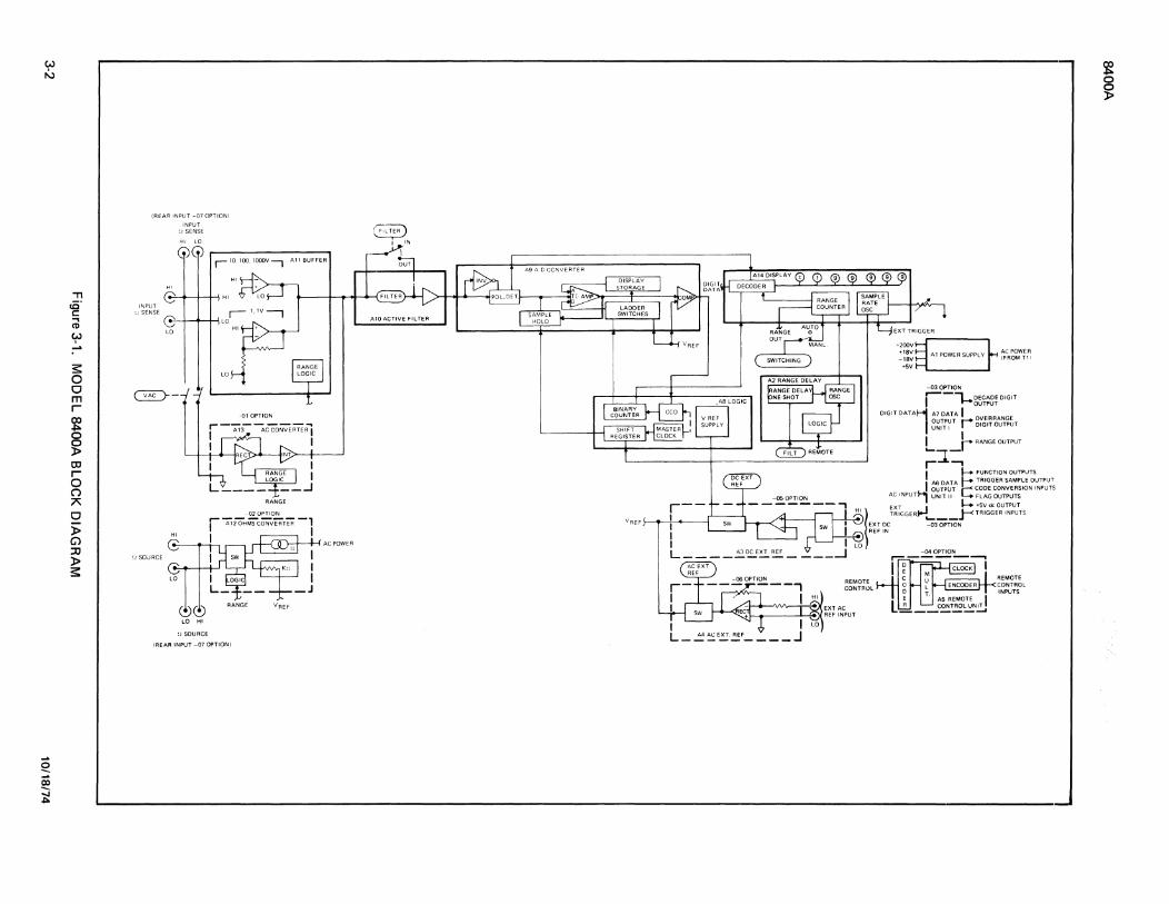
..... e. ..... CX>
~
-n cE' c ""I CD
";-J .....
s: 0 0 m r ~ 0
~ CJ r 0 C") ;;<;
0 )> G') ::0 )> s:
IREAR INPUT -07 OPTION I
INPUT ~! SENSE
>11 LO
G)G) .---------r 10, 100, lOOOV--, A11 BUFFER
INPUT " SENSE r- 1, lV-----,
G'-1-0---1-l LO
LO
~'
G '! SO.JRCE
G LO
~(£) LO HI
'!SOURCE
LO~
-01 OPTION ,-:73- --;CCo~FITT~
I I
RANGE
02 UPTION r Ai20HMS'cON'VE'Rr'ER -, I I
IREAR INPUT -07 OPTION)
AC POWER
I
I I
L----~~~~-- ___ _J
+18V -18V
•SV
Al POWER SUPPLY
-030PTION
AC POWER \FROM TJ,
r-i......g~~~3i DIGIT
DIGIT DATA1 A7 DATA I OVER RANGE OUTPUT r OIGITO TPUT UNIT I U
1 r1 RANGE OUTPUT
'""-:i-r -, I I-+ FUNCTION OUTPUTS
I A6 DATA ~TRIGGER SAMPLE OUTPUT
s-ti OUTPUT ;--<CODE CONVERSION INPUTS AC INPUT I UNIT 11 4 FLAG OUTPUTS
HI EXT • I 1--+ +5V de OUTPUT
©~ TRIGGER,.... .._ __ j-<TRIGGER INPUTS
EXT DC -03 OPTION REF IN
LO
REMOTE REMOTE CONTROL INPUTS
"-+h>----'-~·:• ;.::'""'

to that portion of the A/D amplifier input voltage that caused the amplifier output to be greater than Vref. As the degenerative affect of the primary ladder voltage causes the A/D amplifier output to fall below Vref, the analog amplifier will no longer enable the CCO to send output pulses to the ladder switches. At this point the digitizing process for the most significant digit of the unit input voltage is complete. The voltage level remaining at the output of the A/D amplifier, representing the 8400A input voltage minus the most significant digit, is stored in the sample and hold circuit until the logic control gates it out to the input of the A/D amplifier. Each decade of the recirculated remainder is digitized in a simular fashion with one exception; the recirculated remainder voltage (now the A/D amplifier input voltage) and the primary ladder voltage are now the same polarity, because they are applied to opposite sides of the dual fet input transistor.
3-12. Display (A 14)
3-13. The A 14 Display decodes and digitally displays the input voltage magnitude and polarity. It also provides a variable sample rate for control of the measurement cycle. The circuitry consists of a sample rate oscillator, range counter, decoder, and display indicators. The sample rate oscillator frequency is controlled by a SAMPLE RATE control on the front panel and determines the rate at which the input to the instrument is sampled. The range counter receives auto-range commands from the A2 Range Delay and manual range commands from the front panel switches. The range counter applies range information to the decoder and all input signal conditioning circuitry. Range, polarity, and digit information is processed in the decoder, which then produces the correct display condition in the indicators.
3-14. Range Delay (A2)
3-15. The A2 Range Delay processes switching inputs from the front panel and produces control commands for
the decoder in the Al4 Display. It also produces up/down autorange commands for the range counter. The circuit consists oflogic, range delay one-shot, and a pulse generator. The logic circuitry produces control signals for the pulse generator and the decoder in the A 14 Display. A clock signal for the range counter in the A 14 Display is produced by the pulse generator. This clock signal is required for the autorange feature. The range delay one-shot produces a programmed time delay after any range change to allow for settling time
of analog signal conditioners which process the input.
10/18/74
8400A
3-16. Power Supply (A 1)
3-17. Operating voltages for the instrument are produced in the A 1 Power Supply. The voltages produced are+ 200V, ±18V and +SV. Each voltage is derived from the ac input using a series regulator.
3-18. Options
3-19. Optional features can be installed in the instrument. Each option is shown in Figure 3-1 and described in the following paragraphs.
3-20. AC CONVERTER. The A13 AC Converter is installed as the -01 Option. This circuitry allows ac measurements to 1 OOOV at frequencies from 10 Hz to l 00 kHz. The circuitry consists of an operational rectifier, amplifier integrator, and range logic. AC inputs are amplified or attenuated and rectified in the operational rectifier. The resulting de voltage is then filtered and amplified by the amplifier integrator. Range commands are processed in the range logic whose output then establishes a fixed gain or attenuation factor for the operational rectifier. The resulting full-scale - IOV de output is applied to the AIO Active Filter. This voltage is then filtered, serially digitized and displayed in the same manner as previously described in the basic instrument paragraphs.
3-21. OHMS CONVERTER. The A12 Ohms Converter is installed as the -02 Option. This circuitry allows resis
tance measurements from 100 µQ to 12M n. Resistance measurements in ohms ranges are true, four-terminal. Measurements in K ohm ranges are conventional two-terminal. The circuitry consists of a constant current generator, a current source, switching circuitry, and logic. When the ohm function is selected, the constant current generator output is made available to the n SOURCE terminals. Since both the .Q SOURCE and SENSE terminals are connected to the unknown resistance, the All Buffer input voltage is directly proportional to the resistance value. The A 11 Buffer output is then serially digitized and displayed as described previously to indicate the resistance value. In the K ohm ranges, the current source output is made available to the n SOURCE terminals. The resulting voltage input is then measured in the same manner; however, since the voltage drop in the lead resistance of the unknown also appears at the voltage measuring terminals, true four terminal measurement is not available. Simplified diagrams of the four terminal and conventional resistance configurations are shown in Figure 3-2.
3-3

8400A
3-22.
A
OHMS RANGE CONFIGURATION
~ HI n SOURCE
OUTPUT
LO n SOURCE ---'VV\r---'
'=' LO n SENSE
B K OHMS RANGE CONFIGURATION
~HI n SOURCE
"°" HI n SENSE
LO n SENSE ,-::.,
@ LO n SOURCE
OUTPUT
A12 OHMS CONVERTER
+7V
A12 OHMS CONVERTER
Figure 3-2. OHMS AND K OHMS RANGE CONFIGURATION
DATA OUTPUT. The A6 and A7 Data Output Units are installed as the -03 Option. This circuitry provides parallel, isolated, coded outputs of digit, polarity, range, and function. It also provides a +SV de output for external equipment as well as input lines for external triggering and control of the measurement cycle. The circuitry is contained on two separate assemblies. Digit and range outputs are available from the Data Output Unit 1. Function indications, flag outputs, and +SV de outputs in addition to triggering and code conversion inputs are available in the Data Output Unit II.
3-23. REMOTE CONTROL. The AS Remote Control Unit is installed as the -04 Option. This circuitry allows remote control of mode, instrument range, and functions. Input requirements are compatible with DTL or TTL logic levels. The circuitry consists of a clock generator, encoder, multiplexer, and decoder. The clock generator produces a clock signal which gates the multiplexer and decoder. Inputs are coded in the encoder and applied to the multiplexer. The multiplexer output is then serially transferred to the decoder at the clock rate. Serial to parallel conversion takes place in the decoder and the resulting commands used to control the range and function.
3-24. DC EXTERNAL REFERENCE. The A3 DC External Reference is installed as the -05 Option. This circuitry allows de/de and ac/dc ratio measurements using an external de reference voltage. Input reference voltage can be from +1 to +10.SV de. The circuitry consists of a differ-
3-4
ential amplifier and a switching circuit. The external reference input is buffered by the differentiai ampiifier. Appiication of internal or external reference voltage to the V REF line is done through the switching circuit.
3-25. AC EXTERNAL REFERENCE. The Al4 AC Ex-ternal Reference assembly is installed as the -06 Option. This circuitry allows ac/ac ratio measurements with an external ac reference voltage. Input reference voltage can be from 0.1 to lOOV ac at 10 Hz to 100 kHz. The circuitry consists of an operational rectifier and switching circuitry. The ac reference input is amplified or attenuated and rectified in the operational rectifier. The resulting de reference is then applied to the V REF line by the switching circuitry.
3-26. REAR INPUT. The Rear Inputterminals are installed as the -07 Option. These terminals are connected in parallel with the input terminals on the front panel.
3-27. CIRCUIT DESCRIPTIONS
3-28. The following paragraphs describe in detail the basic circuitry contained in the instrument. Circuit descriptions for options are located in the subsections of Section 6. Schematic diagrams are located at the rear of the manual.
3-29. A 11 Buffer
3-30. The All Buffer (Drawing No. 8400A- l 005) provides a full-scale de voltage, isolated from the input under measurement, of 1 OV de. It consists of four basic elements: input and output voltage dividers, amplifiers, and control logic. The circuitry has two operating configurations or modes determined by the voltage range selected: a low volts mode and a high volts mode. In the low volts mode (O.l and 1.0 volt range) some amplification of the input occurs. In the high volts mode (10, 100, and 1000 volts range) input attenuation occurs, except in the 10 volts range when the input is processed without attenuation or amplification. Both modes are shown in block form in Figure 3-3. The A portion of the figure depicts the low volts mode, and the B portion of the figure depicts the high volts mode.
3-31. The input to the All Buffer is derived from input jacks J25and126, both jacks being shown on the block and system wiring diagrams. Buffer input current limiting resistors lRl and 1 R2 are also located on the system diagram, along with the high and low inputs to the All Buffer, at jacks J4TM and JlTR, respectively, of terminal block No. 1.
3-32. On the All Buffer schematic, the low volts input is applied across current limiting resistor R2, through the contacts of Kl, to the high input impedance amplifier com-
10/18/74

A
LOW VOL TS MODE
(0.1OR1.0 VOLT INPUTI
INPUT
HI INPUT Z AMPLIFIER
8400A
INPUT
TO l J25 Rl R2
CURR ENT 1---..--...i-""'
UPSCALER
LOW VOLTS OUTPUT DIVIDER R37 & R40
OUTPUT TO FILTER TO
10 VOLTS J26
INPUT
LMTR A11R2 AND
>-------1 SWITCHING (Kl &K71
OVLDPTCT R2,CR1,011,
U3 AND TEMP COMP
02& 03
OFFSET AND
COMMON MODE BIAS
FEEDBACK
AND SWITCHING
U3 ___ _.
VOLTAGE FOLLOWER
-10 VOL TS
SELECTION l 1.0 l
VOLT
LOW VOLTS SWITCHING------------------~
LOGIC (Kl & KSI
B
HIGH VOL TS MODE
(10, 100 OR 1000 VOL TS INPUTI
INPUT TO 1000 VOLTS
I J25
J26
INPUT ~~Al-.-,.IV~CURRENT
LMTR A11R2
1<2A .......-;KlB
DOWNSCALER
HIGH VOLTS INPUT
DIVIDER R5-R10 SWITCH-
SWITCHING
K7
HI-INPUT IMPEDANCE INVERSION FOLLOWER OUTPUT
TO FILTER TO -10 VOL TS
ING K3,
HIGH VOLTS SWITCHING LOGIC FOR K2, K3, K4,
OVLD PCTR R2,CR1,011,
U3,AND TEMP COMP
02& 03
Figure3-3_ BUFFER AMPLIFIER BLOCK DIAGRAM
posed of three separate amplifiers: dual differential amplifier Q5 and Q4, operational amplifier Ul, and inverter U2.
3-33. The output of the amplifier is applied in parallel to the AlO Active Filter and to a gain determining, output voltage divider, R37 through R40, through contacts of relays Kl and K6. Inspection of the resistance ratios in the output divider shows that the final amplifier output must be 100 times the input in the 0.1 volt range, and 10 times the input in the 1 volt range. Thus, the All Buffer output is the required 10 volts for full-scale inputs.
3-34. In the high volts mode of operation, shown in Figure 3-3B, the buffer amplifier receives the input voltage directly (lOV range) or receives a scaled down voltage through an input voltage divider consisting of RS through RIO. Since the buffer is a unity gain inverter, its output is the inverse of the received input. For example, an input of
10/18/74
+ l OOOV would be scaled down to +I OV through the input divider. With +lOV at its input, the buffer output is -lOV.
3-35. In the low volts mode, voltage follower U3 is used to bootstrap the operational environment of the input dual differential pair Q4 and QS, with the input voltage to increase its effective ratio of common mode rejection. Any differential amplifier offset voltage present that would cause buffer output with no input is compensated by use of two potentiometers; one, COARSE DC ZERO, which balances the base emitter voltages of the input differential amplifier QS by adjusting the collector current ratio, and two, or the second potentiometer, BUFFER ZERO, which affords a fine adjustment via the front panel by applying just that amount of nulling voltage to the base of differential amplifier QSB that results in a buffer output voltage equal to zero when the input voltage is zero. This last potentiometer is labeled DC ZERO just over the front panel access hole.
3-5

8400A
3-36. Overload protection for dual differential amplifier QS is afforded by the combination of components R2, CRl, Ql 1, and the current limiting resistors previously defined as R1 and R2 shown on the system wiring diagram. Positive overvoltage protection is afforded by transistor Ql 1 which clamps amplifier output to 1.7 volts. Negative overvoltage protection is afforded by diode CRl which clamps the input to -1.7 volts. The current drawn during an overload is limited by the total input resistance of 147k ohms.
3-37. Compensation circuits are provided to reduce the temperature coefficients of the input offset voltage and offset current. Transistor Q2 and surrounding circuitry provides through Rl 8 and Rl 9 the temperature varying base current required by input transistor QS. Transistor Q3 compensates the temperature valiation of the baseemitter voltage in dual transistor Q4 to ensure that input transistor QS remains at substantially the same bias conditions irrespective of temperature.
3-38. A10 Active Filter
3-39. The AlO Active Filter (Drawing No. 8400A-1015) consists of a voltage follower preceded by four poles of low pass filtering. These four poles attenuate undesirable AC signals which may be present in the de input signal. Filtering occurs after the FILT button on the front panel of the DVM is depressed. A block diagram of the active filter is shown in Figure 3-4. Also shown is the response curve of the active filter which plots attenuation in decibels against a log scale of frequency in Hertz.
TO 10 VOLTS AND AC NOISE
ACTIVE FILTER BLOCK DIAGRAM
OUTPUT TO A-TO-D CONVERTER
>-..+-< ... TO 10 VOLTS
3-40. A9 A-to-0 Converter and AS Logic
3-41. The A9 A-to-D Converter and A8 Logic circuits (respectively, drawings No. 8400A-1003 and -1004) are dis· cussed together in the following paragraphs, since any discussion of the analog-to-digital (A-to-D) conversion process must include elements of both circuits. The basic conversion and logic circuitry involved in the conversion process is shown in Figure 3-5. Also shown is an arbitrary input voltage that is the equivalent to the inverted, unknown voltage applied across the input jacks of the DVM. The output of the converter is shown, applied to the following stage, the A14 Display, and consists of binary coded data bit groups that are serially emitted from the converter and applied to the display circuits for decoding and serial display. The basic purpose of the combined converter-logic circuitry is to convert the analog voltage input (given as +6.3524 de volts in Figure 3-5) serially by decade to binary coded bit groups, one bit group per decade.
3-42. The inverting amplifier consists of input switch Q3, dual FET input amplifier Q4, operational amplifier Ul, and associated circuitry. Once every 18 milliseconds, during the C sub-period the inverting amplifier switch Q6 is switched on by the SS Logic Signal, to zero the inverting amplifier. The automatic zero circuit consists of transistors QS and Q6 and capacitor C2. The drive circuit also supplies a turn-off signal to transistor Q3, thereby removing the input to the inverting amplifier during the C sub-period.
ACTIVE FILTER RESPONSE CURVE
~5 1----==-.~ -10
-20 I----+--+---" ...
ATTENUATION
-60 DEC11~E~S _;. _ _,__ _ __, _ ___...
FREQUENCY IN HERTZ
Figure3-4. ACTIVE FILTER
3-6 10/18/74

"TI .c· c .... CD
)>
.'...i 0 0 (') 0 z < m ::0 -f m ::0
)> z Cl
r-0 G)
(')
OJ r-0 (') 7'
Cl )> G) ::0 )> s:
A/D INPUT
+6.3524 DC VOLTS
A/D INPUT +6.3524 vo·L TS
A9 A TOD CONVERTER AND AS LOGIC CIRCUITS
INV AMP 03. 04, 05, 06 &
r U1 POLARITY ~ DET. 04, U1 010, 011
1-FROM AUTOZERO DRIVE
J SWITCH l 1 07
_,{_ DISPLP.Y STORAGE
f 012 THRU 018 j.---C11 THRU C15 U3 ,--
•6V
+6V
J J SWITCH \. l OS J -6 3524V ~ ~ ~
TO INV AMP
J' INV. AMP AUTOZERO DRIVE 01, 02, 03, 05, 06
A9 ATO D CONVERTER AND AS LOGIC CIRCUITS
*ELEMENTS OF LOGIC CIRCUITRY
'--
3.524
SAMPLE & HOLD C9 IV C10 025 THRU 02S
I '""°' } CYCLE CONTROL US, 011 THRU
017 *
OUTPUT BIT GROUPS 0110. 0011, 0101, 0010 aw1 0100 CHARACTERISTIC OF 6 3 2
LADDER R44 BCD THRU R50. 0110 R40, R41. R42. R43, 037 THRU 044
VOLTAGE R~ U9, U10, 023 TH RU 025
*
ANALOG CURRENT BCD COMPARATOR
lilllJJ CONTROLLED COUNTER
035. 032 6 OSCILLATOR U5. U6, R45 033. 045 02 R46, R48, R49, 034 03 R51 019 THRU
l ] * 022
DISPLAY MASTER
J. STORAGE CLOCK
CONTROL C1
06 THRU 010 R1
* 01
J J l SHIFT REGISTER U3. U4. U1A
*
BCD 0110
I--' I
.--------1 --~ ( T615L4 ) G I
A14 DIO::.PLAY L _______ _J
,--------, I (=-~2' _)GJ I I C ___ , I I -- I
OUTPUT BIT Bl~J;i..RY T(~ DECIMAL J DISPLAY
GROUPS) DEC'.:.)[JER - • TUBE I DR~~ER I ~~'\°~OSUUTV_/ 1----sco+
0110 I i I * L __ _ __ _J

8400A
343. The polarity detector consists of flip-flop QlO, Qii, and associated circuitry. The flip/flop employs base triggering, which is applied through diode CR6 to the base of QlO. The gate signal, gate 4, is applied to the emitters of Q l 0 and Q 11 and enables the detector during the A subperiod of the measure period. During the remainder of the measure period, the plus and minus gates (Q8 and Q7, respectively) are turned off and the polarity information is retained by the display circuitry.
344. The A/D amplifier consists of dual FET Q20, operational amplifier U2, and associated components. Switch Q24 is turned on during the ZERO (f)) sub-period of the measurement period by a ZERO signal from the logic circuit. This signal also controls switches QI 9 and Q3 I, which are turned on during the ZERO sub-period to zero the differential amplifier, and switch Q30, which is turned off during the ZERO sub-period to disconnect the amplifier output from the ladder. Transistor Q29 and resistor R54 constitute a clamp, which prevents amplifier U2 from saturating while its output is above 7 volts.
345. The analog comparator, consisting of transistors
Q45, Q32, Q33, Q34, Q35 and associated components, is basically a voltage comparator. Differential amplifier stage Q35 compares the A/D amplifier output with the +7 volts reference, and differential stage Q33, Q34 outputs to the current controlled oscillator (CCO) anytime the A/D amplifier output voltage is greater than the +7 volts reference. Transistor Q32 operates as a second comparator, which responds quickly to high voltage levels, thereby allowing maximum time for resolution of the least significant digit.
346. The sample and hold circuit consists of transistors Q25 through Q28 and capacitors C9 and Cl 0. The sequence of operation for the sample and hold circuit is shown in Figure 3-6.
MEASURE SWITCHES VOLTAGES STORED ON PERIOD ON SAMPLE AND HOLD CAPACITORS
SUBPERIODS C9 C10
A 026, 022 3.524 0 B 025, 028 3.524 5.24 c 027,026 2.4 5.24 D 025, 028 2.4 4.0 E 027 0 4.0
ZERO (0) 019, 031, 0 ? 024
[!::> VOL TAG ES SHOWN ARE ONLY PROPORTIONAL TO ACTUAL VOLTAGES.
Figure 3-6. SAMPLE AND HOLD SWITCHING
3-8
3-47. The ladder switches of Q37 through Q44 are controiied by drivers Q 19 through Q22 on the A8 logic board. The output of the ladder switches is applied to two ladders. Each ladder comprises a 4-bit, weighted-resistor, digital-toanalog converter. The primary ladder consists of resistor~ R44 through R50 and produces an output voltage that corresponds to the actual value of the most significant digit of the A/D amplifier input voltage. The secondary ladder, which drives only the display storage circuit through buffer amplifier U3, consists of resistors R40 through R43 and produces an output that closely approximates the actual value of the primary ladder output. A half-digit bias is produced by R38 and R39 in conjunction with the secondary ladder resistors and adds the voltage equivalent of a half-digit to the output of the secondary ladder. This ensures proper display storage readout by compensating for the effects of voltage decay in the storage circuit.
348. The display storage circuit consists of FET switches Q13 through QI 7, capacitors Cll through CIS, and FET switches QI 2 and QI8. The buffered output of the secondary ladder is supplied to the appropriate storage capacitor through QI8, which is switched on during the second half (display time) of each sub-period. The first (most significant) digit is stored on C 13, the second on C 11, etc. When the cycle change circuitry switches to storage mode, Ql2 is turned on and the analog voltages stored on the storage capacitors are serially applied to the input of the A/D amplifier. Thus, the same reading is continually digit
ized and displayed until a new sample of the input is taken.
349. The 333 Hz clock signal is produced by transistor QI on the AS Logic board. The clock frequency is determined by the RC time constant of resistor Rl and capacitor C 1. The output of QI is applied to the trigger input of flip-flop UlB. The F output of U lB is inverted in Q4 an·d
becomes the H signal. The F, F, and H signals are used by the logic to generate control signals.
3-50. The six-state shift register consists of J-K flip-flops U3A, U3B, U4A, U4B, and UlA. Error correction gate U2B controls the input to flip-flop U3B to ensure proper operation of the shift register. At the end of a typical digitizing cycle, flip-flop U l A reverts to the ZERO condition upon receiving the H clock pulse. Since all the flipflops are now in the ZERO condition, the output of U2B goes low, thereby defining the start of the ZERO subperiod as shown in the timing diagram of Fi~re 3-9. The ZERO sub-period is terminated by the next H clock pulse, which sets flip-flop U3B high because its J input was high and its K input was low when the clock pulse was received. Subsequent clock pulses set the flip-flop outputs as shown in Figure 3-7.
10/18/74

SHIFT REGISTER FLIP FLOP AND ZERO GATE
SUBPERIOD ~~-.-~~....-o_u_T_P~U~T_s_T_A_T_ETS~~-r~~-i
ZERO
D E
U3B U3A U4A
0 0 0 0
0 0 0 0 0 0
U4B
0 0
0
U1A
0 0
0
Figure 3-7. SHIFT REGISTER OUT PUTS
U2B
0
3-51. The sixteen-state binary counter consists of J-K flip-flop USB, USA, U6A, and U6B. The counter is set to ZERO at the beginning of each sub-period in the measure
ment period by the H clock pulse . During each subperiod of the digitizing cycle, the output pulses from the CCO, which are applied to the clock input of flip-flop USB, are counted. The truth table for the flip-flops in the binary counter is shown in Figure 3-S . The binary counter is disabled by gate U2A if the count of 11 is attained.
cco SIXTEEN-STATE PULSE BINARY COUNTER COUNT U5B U5A U6A U6B
z y x w
0 0 0 0 0 0 0 0
Figure 3-8. SIXTEEN-STATE BINARY COUNTER OUTPUT
3-52. The CCO consists of multivibrator Q2 and Q3 . The CCO has no output until it is supplied current by the
analog comparator and is enabled by the F output of the J-K flip-flop UlB. The CCO output is applied to the clock input of the 16-state binary counter. The 9's catcher gate
U7 A, disables the CCO at a count of nine, if the DVM is digitizing the second through fifth digits (sub-periods B through E).
3-53. The outputs of the six-state shift register , in conjunction with the H pulses of the output of Q4, are applied to the display storage control circuit consisting of transistors Q6 through QlO and related components. Outputs
10/18/74
8400A
from this circuitry control the display storage circuit located on the A9 A·to-D Converter board .
3-54. The analog cycle control circuit produc s the gating and control signals which are used to control the synchronization of events in the analog portion of the bvM, principally in the A-to-D Converter circuits . These signals, together with other control signals are shown in the DVM Timing and Synchrony Diagram , Figure 3-9. The
analog cycle control circuit consists of NAND gates USA
through D driving transistors Q 11 through Q 17 and associated circuit elemen ts.
3-55. The ladder switch driver circuitry (Q 19 through Q22 on AS Logic board) receives S-4-2-1 coded binary data from the sixteen-state binary counter and translates this to
4-4-2-1 coded binary data , which matches the weighting of the resistors in the ladder. Thus , the ladder output is proportional to the count in the binary counter. The count increases until the output of the ladder is sufficient to bring the A-to-D amplifier to the particular balanced position required by the input voltage .
3-56. The master +7 volts reference for the instrument is derived using reference amplifier U9 as a reference element. The reference voltage is produced using operational amplifier UIO and emitter follower Q25, which presents a low source impedance at the reference point. Transistor Q24 disables the +7 volts reference in the event the user wishes to employ an external reference and the required options are installed. Transistor Q23, coupled with the
zener in the reference amplifier, produces a reference voltage for the·+ 1 S volts regulator in the Al Power Supply.
3-57. A14 Display
3-SS. The A14 Display circuits (Drawing No. S400A-
1002) control the function/status indicators and the decimal indicators associated with the readout tubes. The KD. ,
AC , DC , n, OVER, FILT, and X REF indicators are controlled by the respective function control lines. They are illuminated when +5 volts de is applied to the control line ; however, the control lines are interlocked in the associated assembly so that the indicator remains extinguished unless
the assembly is installed in the iµstrument. The OVER range indicator is operated by transistor QS in the OVER
RANGE DRIVER circuit.
3-59. The polarity signs + and - of tube V 1 are con· trolled by a flip-flop consisting of transistors Ql9, Q20, FET switches Q32, Q33, current source transistors Q9,
3-9

8400A
3-10
OPERATO R
MASTER CLOCK
A801
A8U1B
A804
F
R
~j4-5µs
IDEALIZED OUTPUT
A8U3B
A8U3A ::1 11,~1~· ~-
A8U4A
A8U4B
A8U1A
: ===n:n--1~:::1
!i1
.~ii .......... iii.__: n_ ~n---l .___n_-_-_-
0..---____ ....,l.UIH lllllilllllllli~' .... 1 ..... 1 ___ ___, A8U2B
A8U2B (TIME SCALE COMPRESSED) 0
A1408 (SAMPLE RATE FREQUENCY)
MEASURE/ STORAGE CYCLE
MEASURE PERIOD EXPANDED
5 6 7 8 I
_ll'---+-----------l~'-----1
I I i D f E
!+-(NO DELAY)
>---S-T-0-RA_G_E--~ STORAGE
I I I 0 A B c D E 0 ~ A ~ ~
MEASUREMENTS SUB-PERIODS
Figure 3-9. DVM TIMING AND SYNCHRONY DIAGRAM (SHEET 1)
WAVEFORM NO.
1.
2.
3.
4.
5.
6.
7.
8.
9.
10/18/74

OPERATOR
A14U3A
A14U3A
(MEASU RE
PE RIOD
EXPA NDED)
A8Q4
A8014
A8016
A80 15
A8017
10/18/74
I t E
IDEALIZED OUTPUT
5- STORAGE -l·M-1•4--- ME1SUR E ----llilM-14--- STORAGE -f
I I ' D ; E
I
0
0
A
A B c D
SUBPER IODS MEASU REMENT
B c
E
D E
Figure 3-9. DVM T IMING AND SYNCHRONY DIAGRAM (SHEET 2)
8400A
WAVEFORM
NO.
9.
I 0 + A 9A.
3A.
10.
11.
12.
3.
3-11
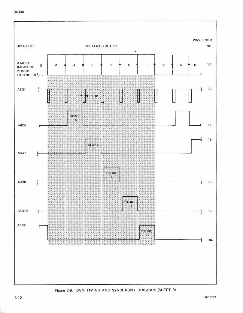
8400A
WAVEFORM
OPERATOR IDEALI ZED OUTPUT NO.
" I I
0 A B c D E 0 T A T B 9B.
I I
A8Q4
~ Li 3B .
A8Q6 L 14.
r 15.
A807
Figure 3-9. DVM TIMING AND SYNCHRONY DIAGRAM (SHEET 3)
3-12 10/18/74
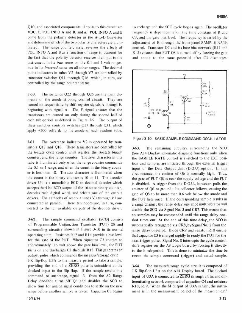
QI 0, and associated components. Inputs to this circuit are
VDC, C, POL INFO A and B, and a. POL INFO A and B
come from the polarity detector in the A-to-D Converter
and determine which of the two polarity characters are illum
inated. The range counter, via a, reverses the effects of
POL INFO A and B as a function of range to account for
the fact that the polarity detector receives the input to the
instrument in its trne sense on the 0.1 and 1 volt ranges,
but in its inverted sense on all other ranges. The decimal
point indicators in tubes V2 through V7 are controlled by
transistor switches Ql I through Ql6, which, in turn, are
controlled by the range counter status.
3-60. The switches Q22 through Q26 are the main cle
ments of the anode strobing control circuit. They are
turned on sequentially by shift register signals A through E,
beginning with signal A. The F signal ensures that the
transistors are turned on only during the second half of
each sub-period as defined in Figure 3-9. The output of
these switches controls switches Q27 through Q3 l, which
apply +200 volts de to the anode of each readout tube.
3-61. The overrange indicator V2 is operated by tran
sistors Ql 7 and Ql8. These transistors are controlled by
the 6-state cycle control shift register, the 16-state binary
counter, and the range counter. The zero character in this
tube is illuminated only when the range counter commands
the 0.1 or l range, and when the count in the binary count
er is less than I 0. The one character is illuminated when
the count in the binary counter is I 0 or 11. The decoder
driver U4 is a monolithic BCD to decimal decoder which
accepts the 4-bit BCD output of the 16-state binary counter,
decodes each digital word, and selects one of ten output
drivers. The cathodes of readout tubes V3 through V7 are
connected in parallel. These ten nodes are, in turn, con
nected to the ten available outputs of the decoder driver.
3-62. The sample command oscillator (SCO) consists
of Programmable Unijunction Transistor (PUT) Q8 and
surrounding circuitry shown in Figure 3-10 in its normal
operating state. Resistors Rl 2 and Rl4 provide a bias level
for the gate of the PUT. When capacitor C3 charges to
approximately 0.6 volt above the gate bias level, the PUT
turns on and discharges C3 through R 15. This generates an
output pulse which commands the measure/storage cycle
J-K flip-flop U3A to the measure period to take a sample,
providing the end of a ZERO pulse is coincident at the
clocked input to the flip flop. If the sample results in a
command to autorange, signal 3 from the A2 Range
Delay one-shot turns off Q6 and disables the SCO to
allow time for analog signal conditions to settle on the new
range before another sample is taken. Capacitor C3 begins
10/18/74
8400A
to recharge and the SCO cycle begins again. The oscillator
frcqL1cncy is dcpen\knt upu11 the ti111c cunstant or Rand
C3, and the gate h;Js level. The frequency is varied hy the
adjustment uf R through the front panel SAMPLE RATE
control. Transistor Q7 and its base bias network (Rl 1 and
R 13) ensures that PUT Q8 is turned off by forcing the gate
and anode to the same potential after CJ discharges.
12K
R14 33K
R 12
75K
•5V
1C3
20 µf
Figure 3-10. BASIC SAMPLE COMMAND OSCILLATOR
3-63. The remaining circuitry surrounding the SCO
(See Al 4 Display schematic diagram) functions only when the SAMPLE RATE control is switched to the EXT posi
tion and samples are initiated through the external trigger
input of the Data Output Unit (D.O.U) option. In this
circumstance, the emitter of Q6 is normally high. Thus,
the gate of PUT Q8 is near the supply voltage and the PUT
is disabled. A trigger from the D.O.U ., however, pulls the
emitter of Q6 to ground. Its collector follows, causing the
gate of Q8 to be more than 0.6 volt below the anode and
the PUT fires once. If the corresponding sample results in
a range change, the range delay one shot multivibrator will
disable the SCO via Signal No. 3 and CR7. This means that
no samples may be commanded until the range delay one
shot times out. At the end of this time delay, the SCO is
automatically retriggered via CR8, by Signal No. 2 from the
range delay one-shot. Diode CR9 and resistor Rl 0 ensure
that capacitor C3 is charged rapidly to ready the PUT for the
next trigger pulse. Signal No. 8 interrupts the cycle control shift register on the AS Logic board by forcing it directly
to the E sub-period. This is done to minimize the time be
tween the sample command (trigger) and actual sample.
3-64. The measure/storage cycle circuit is composed of J-K flip-flop UJA on the Al4 Display board. The clocked
input of U3A is connected to ZERO through a bias and dif
ferentiating network composed of capacitor C4 and resistors Rl8, Rl9. When the M output of U3A 1shigh, the instrument is in the measurement period of the measurement/
3-13

8400A
storage cycle. When the M output from U3A is low, the
storage period prevails. The clocked input is normally high
as determined by the bias network, and since this is a master-slave type flip flop, the master is connected directly
to the J and K inputs and isolated from the outputs. If the SCO outputs a pulse, the J input goes high and causes
the master to assume the true state. At the start of the
next ZERO (0) time, the clock pulses low causing the slave,
and, hence, the outputs, to assume the state of the master.
That is to say, the output goes true and initiates a measure
cycle. At the same time, the master is updated as a func
tion of the new J and K inputs. Thus, at the start of the
next ZERO (0) time, the slave assumes the false state
existing in the master, and the storage period is initiated.
Not until the SCO pulses again will another measurement
period be initiated. The idealized waveform output of the
measure/storage cycle J-K flip-flop is seen by viewing wave
form No. 8 and its two input generating waveforms 6 and 7
in Figure 3-9, Sheet 1.
3-65. The OVER RANGE DRIVER circuit is composed
of programmable unijunction transistor (PUT) Q4, tran
sistors Q3, QS, and Q37, and associated circuitry. Tran
sistor Q2, diode CRS, and resistors R2 and R4 are not part
of the driver circuit but constitute a delay line in the speed
at which the range delay one-shot multivibrator circuit on
the A2 Range Delay board times out. The time-out delay is
a function of the FIL Ter button being depressed on the
front panel, applying a low at the base of PNP transistor
Q2, turning it on, and effectively holding transistor QI in
the range delay one-shot off (time-out status) for a longer
time than would otherwise occur if transistor Q2 were not
turned on by the filtering function being activated. The
overrange driver PUT Q4 is turned on when its gate voltage
is depressed about 0.6 volt relative to the anode voltage.
The differential voltage developed across resistor R64 (tied
between the gate and anode of the PUT) when the PUT
conducts turns on PNP transistor QS, and resultingly, turns
on the OVER lamp in the function display annunciator.
The gate to anode voltage relationship that turns on tran
sistor QS and the OVER lamp is brought about by NPN
transistor Q3 when it is turned on. Q3 is turned on by the
12th output pulse from the CCO being applied to its base.
Twelve output pulses from the CCO indicate greater than
twenty percent overvoltage is being applied at the input of
the instrument for a given range. However, even though
turned on, transistor Q3 is ineffective in gating the PUT
unless an t•nabling signal (UP) is applied through Rb tu its
emitter. The source of the UP signal is the outrut of
~AND gate U2A located on the A8 Logic board. Signal
No. 7 is the UP range signal that is applied to NANO gate
U3B on the A2 Range Delay board. It is generated at the
emitter of transistor Q3 7 when this transistor is turned on
3-14
by the PUT firing. After firing, the PUT is reset by the
application of the positive-going edge of the M signal
applied to its cathode through C 1.
3-66. The RANGE COUNTER circuit is composed of
J-K flip-flops U2A and U2B. The clocked input to the
range counter is provided by J-K range flip-flop U3B, that
has as its clocked input signal No. 6. This signal originates
in the range oscillator on the A2 Range Delay board and is
pulsed high everytime the range oscillator PUT fires. The
J-K inputs to the range flip-flop U3B are tied together at
the output of the measure/storage cycle J-K flip-flop U3A
and go high every measurement period. The range counter is a divide-by-6 counter that provides the 6 possible binary
states for range counting, S pulses being considered an up
range command and 1 pulse being considered a down
range command. Signal No. 6 applied to the clocked input
of the range flip-flop U3B alters the 6 states of the range
counter. Transistor Q35 is provided to pull the range
counter out of an unallowed state that may occur at turn
on.
3-67. A2 Range Delay
3-68. The A2 Range Delay circuits (Drawing No. 8400A-
1006) consists of a series of gates, a range delay one-shot
multivibrator, and a range oscillator. The gates allow the
specified set of ranges to be attained, which is dependent
upon the function called on the front panel. The range
oscillator generates pulses which trigger the range delay
one-shot while simultaneously causing the A14 range
counter to change states. The range delay one-shot pre
vents further ranging for a specified time to allow the ana
log signal conditioners to settle in the new range.
3-69. The gates are U2A, U2B, U2C, U3A, and U3B.
Gates U2C and U3A are up range stops which pull down on
the range-up enable line. Gate U2C prevents autoranging
above the 10,000 range, while gate U3A prevents auto
ranging above the 1000 range on the VDC function. Gates
U2A and U2B are down range stops which pull down on
the range-down enable line. Gate U2A prevents autorang
ing below the 10 range in the .Q function, while gate U2B
prevents autoranging below the 0.1 range in any function.
Gate U3 B is the master up-range control. It enables the
range oscillator only if an up range is to be expected.
3-70. The three inverters UlD, UlE, and UlF coupled
with the range-up enable line provide one input for up
range control gate U3B. The result is that U3B is enabled
for 1.5 milliseconds (the second half of the A sub-period
of a measurement period) if an up-range is to be executed.
10/18/74

Signals applied to diodes CR6 through 8 and 10, coupled with the range-down enable line provide a negative going signal to the range oscillator at the end of the A subperiod of a measurement period if a down-range is to be executed. Thus, there are two ways which can enable the range oscillator.
3-71. The range oscillator is composed of capacitor C4,
resistors R 14andR18, and Programmable Unijunction Transistor (PUT) Q4, with the output of this oscillator appear
ing at the cathode of PUT Q4. The PUT is fired, discharging capacitor C4 through RlS, when the gate is about -0.6 volt
relative to the anode. Thus the PUT is fired to produce one output pulse by lowering gate voltage or by raising the anode voltage, such that the voltage difference between
these elements is as indicated above. The firing of PUT Q4 discharges capacitor C4 and reduces the anode and gate voltages. This causes Q3 to turn on and force the anode
and gate of Q4 to the same potential. Q4 turns off and
capacitor C4 charges through Rl4 and Rl8. If the firing potential between the gate and anode of Q4 is established, Q4 again fires and the cycle is repeated to produce the second output pulse. The frequency of oscillations is set by the level of gate voltage applied and the charging time
constant of Rl4, RIS, and capacitor C4.
3-72. Control of the gate of PUT Q4 is effected by one of two mutually exclusive inputs. One of these is associated with ranging up and is identified on the A2 schematic as the output of gate U3B. The other of the two inputs is associated with ranging down and is identified as the range down enable line. In an up-range situation, the
output of U3B pulls low for l .S milliseconds during which time the range oscillator outputs five pulses. In a downrange situation, the range-down enable line pulls low. This signal is capacitively coupled via C3 to the gate of PUT Q4 causing it to output one pulse. Five pulses counted by the Al4 range counter commands a transition to the next
higher range, while one pulse commands a transition to the next lower range. ln either case, the first output pulse triggers the range delay one-shot to allow the analog signal conditioners to settle in the new range.
3-73. Transistors QI, Q2, and associated components make up the range delay one-shot multivibrator. A range change pulse from the range oscillator applied to the base of transistor Q2 turns this transistor on and transistor Q 1 off, thereby placing the one-shot multivibrator into its
unstable state. The RC charge time of combined capacitors C2, C6, and resistor RS, and the current through Rl6 determine how long the one-shot remains in its unstable state. With the filter selected, no current flows through RI 6 and the timeout is about 220 milliseconds. Without
10/18/74
8400A
the filter selected, the timeout is decreased to about 2S milliseconds because some current flows through Rl 6. Signal No. 3 disables the sample command oscillator during the range delay time. Signal No. 2 re-triggers the SCO at the end of the range delay time.
3-74. Transistor QS and associated components is a circuit that prevents the instrument remaining in a disallowed range, as in 10,000 VIX, when turned on. When
QS is turned on by the inputs of VIX and a. b. c., the collector of QS pulls down on the set line of the counter and thereby forces the instrument out of the 10,000 range.
3-75. A 1 Power Supply
3-76. The Al Power Supply (Drawing No. 8400A-1001) consists of four regulators, a+ and -18 volts regulator, a 200 volts regulator, a S volts regulator. The purpose of the power supply is to furnish to the instrument all of its required operating power.
3-77. The + 18 and -18 volts regulators obtain filtered de voltage from the full-wave rectifiers consisting of diodes CRS through CRS and filter capacitors C2 and CS. The + 18 volts regulator consists of operational amplifier U 1 and series pass transistor Q3. The voltage reference for the + 18 volts regulator is derived from reference amplifier U9 and temperature compensation transistor Q23 on the AS Logic board. The -18 volts regulator consists of operational amplifier U2 and series pass transistor QS. The -18 vol ts regulator is referenced to the + 18 volts.
3-78. The +200 volts regulator is operated from a fullwave bridge rectifier and filter consisting of diodes CRI through CR4 and capacitor C 1. The reference for the +200 volts regulator is the +18 volts. Voltage variations are
amplified in transistor Q2 and applied to series pass transistor QI.
3-79. The +S volts regulator is operated from a full-wave rectifier and filter consisting of CRlO through CR13 and
capacitor C8. The reference for the +S volts regulator is -18 volts. The series pass element is a compound-emitter follower composed of transistor QS driving power transistor Q6 voltage variations which are detected by the sample string (R14, Rl S and Rl 7) are amplified by transistors Q7.
3-80. Miscellaneous Circuitry
3-81. Input power to the instrument and interconnection of various assemblies is shown in the Wiring and Interconnect Diagrams (Drawing No. 8400A-l 000 and
3-15

8400A
8400A-1100). Line power is fused by F 1 and applied through the contacts of POWER switch S 1 and Tl. The primary of Tl consists of two windings which are parallel or series connected through slide switch S2 to allow operation from either a 115 or 230V ac line. When S2 is set to 115, the primary windings of Tl are connected in parallel.
3-16
The 230 position of S2 connects the windings in series. Secondary windings of Tl provide ac voltages to the Al Power Supply and A6 Data Output Unit No. 2. Shielding between the primary and secondary windings prevents coupling of any undesired line signals to the internal sections of the instrument.
4-1. INTRODUCTION
4-2. This section contains information and instructions concerning preventive and corrective maintenance for the Model 8400A Digital Voltmeter. The information and instructions are arranged under headings of "SERVICE INFORMATION, GENERAL MAINTENANCE, PERFORMANCE TEST, CALIBRATION PROCEDURE, COMPENSATING COMPONENT SELECTION, and TROUBLE
SHOOTING."
4-3. A calibration interval of 90 days is recommended
to ensure instrument operation within the 90-day specifica
tions as stated in Section l.
4-4. Table 4-1 lists the required test equipment. If the
recommended equipment is not available, other equipment having equivalent specifications may be used.
Table 4-1. REQUIRED TEST EQUIPMENT
EQUIPMENT RECOMMENDED FUNCTION
NOMENCLATURE EQUIPMEf\IT
DC Calibrator Fluke Model 332D Performance Test
DC Calibrator Calibration
Troubleshooting
Kelvin Varley Fluke Model 720A Calibration
Divider
Differential Voltmeter Fluke Model 885AB Performance Test
Calibration
Troubleshooting
Oscilloscope Tektronix Model 504 Troubleshooting
Oscillator Hewlitt Packard Troubleshooting
Model 745 and 746
8400A
Section 4
Maintenance
4-5. SERVICE INFORMATION
4-6. Each instrument that is manufactured by the John Fluke Mfg. Co., Inc. is warranted for a period of one year upon delivery to the original purchaser. The WARRANTY is located at the front of the manual.
4-7. Factory authorized calibration and service for each Fluke product is available at various world-wide locations. A complete list of these authorized service centers is located at the rear of the manual. Shipping information is given in Section 2, paragraph 2-5. If requested, an estimate will be provided to the customer before any repair work is begun on instruments that are beyond the warranty period.
4-8. GENERAL MAINTENANCE
4-9. Access/Disassembly
4-10. The following procedure is used to gain access to the interior of the Model 8400A.
a. Remove top dust cover to gain access to calibra· tion adjustments and test points.
b. Remove top guard chassis by removing the four screws which hold it in place. Access is now provided to the plug-in assemblies shown in Figure 4-1.
4-1

8400A
A1 A2 A3 A4 A5 A6 A7 A9
Figure 4-1 . ASSEMBLY LOCATIONS
4-2
c. Remove bottom dust cover. By removing single
screw securing bottom guard cover access can be
gained to the bottom section of the Model 8400A.
4-11. Cleaning
4-12. Clean the instrument periodically to remove dust,
grease, and other contamination. Use the following proce
dure:
a.
b.
Clean the interior with clean, dry air at low pres
sure. When the printed circuit boards require
cleaning, first spray them with Freon T.F. De
greaser (Miller Stephensen Company, Inc.) and
then remove the dirt with clean, dry air at low
pressure.
CAUTION
Do not spray Freon T .F. on the component
side of any PCB since damage to certain com
ponents may result.
Clean the front panel and exterior surfaces with
anhydrous ethyl alcohol or a soft cloth dampened
in a mild solution of detergent and water.
CAUTION!
Do not use aromatic hydrocarbons or chlorin
ated solvents on the front panel, because they
will react with the Lexan binding posts.
4-13. Fuse Replacement
4-14. One fuse is located in the rear panel fuseholder.
When replacement is necessary, install Bussman, TYPE
AGC l/2A as shown on Decal located on the rear panel.
4-15. Lamp and Tube Replacement
4-16. The readout tubes (VI thru V7) and the Function
Display Lamps are mounted behind the left portion of the
front panel. These components are replaced without spe·
cial tools using the following procedure:
4-17.
a.
b.
c.
10/18/74
FUNCTION DISPLAY LAMPS
Remove top and bottom dust covers and inner
guard chassis covers.
To replace the function display lamps remove the
function display assembly mounting screws. Ac
cess to these mounting screws is from the bottom
of the instrument.
Remove the function display assembly from the
top of the instrument. After removal of the plexi-
8400A
glass cover on the assembly, the defective lamp
may be replaced by carefully unsoldering the old
lamp, clearing the holes of solder, and soldering
in the new lamp. Instruments below serial num
ber 208 have an extra lamp in FUNCTION Dis
play assembly in position marked MV. All instru
ments above serial 209 do not have a spare
lamp.
CAUTION!
Use a desoldering tool and exercise extreme
caution to avoid lifting land patterns.
4-18. READOUT TUBE REPLACEMENT
a. To replace the readout tubes desolder the base
mounting pins and remove tube from the top of
the instrument.
4-19. The SAMPLE RATE indicator (DSI) is located
next to the SAMPLE RATE adjustment on front panel.
Remove DSI by desoldering both leads from Al4 assembly,
and pull lamp out from holder. Install and solder new lamp.
4-20. Switch Maintenance
4-21. The following procedure covers service and replace
ment of the push button switches. If switch contacts are de
formed, or if switch module is defective, replacement parts
can be obtained by ordering either the FUNCTION or
RANGE switch assembly.
4-22. The procedure for servicing the FUNCTION and
RANGE switch assembly is as follows:
4-23. GENERAL.
a.
b.
c.
d.
4-24.
a.
Remove the top and bottom dust covers and the
top and bottom inner guard covers.
Set all switches to the nondepressed position.
Remove shorting links from INPUT terminals on front panel.
Remove knob from the SAMPLE RATE potentio
meter.
REMOVAL OF DISPLAY PCB.
Unplug and remove all plug in circuit assemblies
from instrument.
4-3

8400A
b. Remove decals from the side of handles.
c. Remove four (4) screws on side of each handle.
d.
e.
f.
g.
Remove the front panel from the instrument.
Disconnect wires from terminal posts to terminal block at the terminal block, and pull SAMPLE
RATE lamp out from its holder.
Remove four (4) screws which secure the front
sub-panel to the inner chassis and three (3) screws
which secure DISPLAY PCB (Al4) to front subpanel. Remove front sub-panel.
Remove seven (7) mounting screws from the dis
play PCB (Al4).
Pull display PCB out from front of instrument.
4-25. DISASSEMBLY - FUNCTION SWITCHES (EX
CEPT EXT REF, FILT).
a.
b.
c.
Unplug Pl4 (flexible plug in circuit plug) from
connector 114 on DISPLAY PCB.
Remove four (4) mounting screws which secure FUNCTION switches to switch assembly brackets.
Remove button on switch to be repaired by ap
plying pressure to the rear of the button on pull
ing button away from switch. Note that on some
instruments buttons are cemented on the switch
shaft. When replacing buttons, use a small amount of contact cement. Apply cement to shaft only.
SWITCH NO. B 9 10 REAR BRACKET
LOCKOUTS x LATCH BAR
LATCH SPRING x LATCH CODE PP pp IL
d.
e.
f.
g.
h.
i.
j.
11 12
x x
IL IL
Pull FUNCTION switch assembly away from brackets.
Remove rear support bracket and lockouts by bending all locking tabs on rear support bracket, up. (Figure 4-2).
Remove retaining ring and spring from switch shaft.
Insert a tool between the latch bar and switch
shaft on adjacent switch (Figure 4-3).
Slide latch bar to edge of opening in front switch support bracket.
Holding latch bar open, push defective switch shaft out rear of module. Switch contacts will fall out of their slots when shaft is pushed out of module.
CAUTION!
Under no circumstances MUST attempts be made to re-form or add tension to the switch contacts by bending them.
13
x
IL
Inspect the switch contacts for contamination
and, if necessary, clean them with a clean swab
saturated in alcohol. After cleaning, the contacts
must be re-coated with a thin coat of grease: Use
RYKON 2EP grease (American Oil Co.) or equiva
lent.
14
IL
CODE IL= INTERLOCKED PP = PUSH PUSH X= LOCATION
LOCKOUTS
4-4
REAR SUPPORT BRACKET
LATCH BAR
BUTTON
SPRING
RETAINING RING
Figure 4-2. FUNCTION SWITCH ASSEMBLY

1. RE LEASE SWITCH SHAFT BY ...
DETAIL A
SWITCH BEING DISASSEMBLED
DETAIL B
SWITCH SUPPORT
SWITCH MODULE
8400A
2 .... INSERTING TOOL BETWEEN SHAFT AND LATCH BAR OF ADJACENT SWITCH AND SLIDING LATCH BAR TO EDGE OF OPENING IN SWITCH SUPPORT.
3. PUSH SHAFT OUT REAR OF SWITCH MODULE
1. SLIDE SWITCH SHAFT OUT REAR OF MODULE
2. SWITCH CONTACTS WILL FALL OUT OF THEIR SLOTS IN THE SHAFT WHEN SHAFT IS REMOVED. ORIENTATION FOR REPLACEMENT MUST BE AS SHOWN.
Figure 4-3. PUSHBUTTON SWITCH DISASSEMBLY
4-26. DISASSEMBLY - RANGE SWITCHES. e. Desolder and remove 114 connector from Display PCB.
a. Unplug Pl 4 (flexible plug in circuit plug) from 114.
b.
c.
d.
Remove U2 and U3, on Display PCB, from their sockets.
Remove four (4) mounting screws which secure RANGE switches to switch assembly brackets.
Pull FUNCTION switch assembly, with brackets, away from RANGE switch assembly.
f. Straighten all locking tabs on rear support bracket.
(Figure 4-4.)
CAUTION!
When straightening locking tabs avoid damaging land patterns on PCB.
4-5
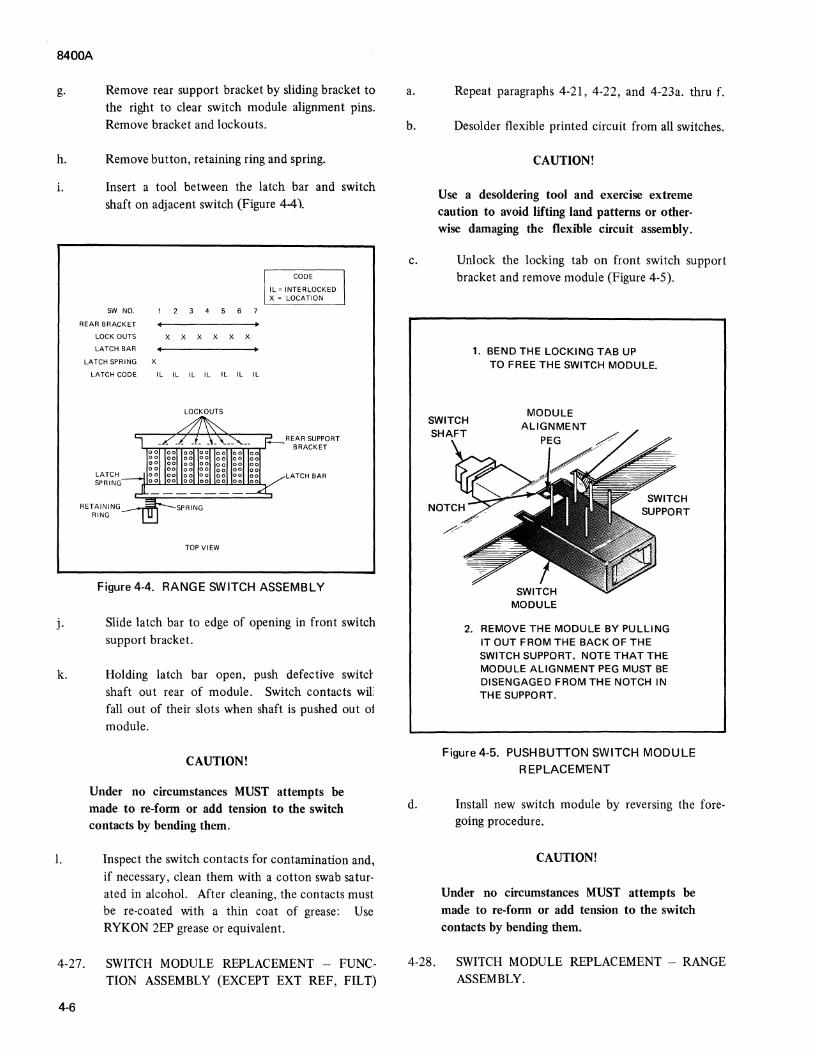
8400A
g.
h.
i.
j.
k.
I.
Remove rear support bracket by sliding bracket to the right to clear switch module alignment pins. Remove bracket and lockouts.
Remove button, retaining ring and spring.
Insert a tool between the latch bar and switch shaft on adjacent switch (Figure 4-4).
SW NO. 1 2 3 4 5 6 7
REAR BRACKET
LOCK OUTS
LATCH BAR
LATCH SPRING X
x x x x x x
LATCH CODE IL IL IL IL IL IL IL
LATCH SPRING
RETAINING RING
LOCKOUTS
TOP VIEW
CODE
IL= INTERLOCKED X = LOCATION
REAR SUPPORT BRACKET
LATCH BAR
Figure 4-4. RANGE SWITCH ASSEMBLY
Slide latch bar to edge of opening in front switch support bracket.
Holding latch bar open, push defective switd shaft out rear of module. Switch contacts wil! fall out of their slots when shaft is pushed out ol module.
CAUTION!
Under no circumstances MUST attempts be made to re-form or add tension to the switch contacts by bending them.
Inspect the switch contacts for contamination and, if necessary, clean them with a cotton swab saturated in alcohol. After cleaning, the contacts must be re-coated with a thin coat of grease: Use RYKON 2EP grease or equivalent.
4-27. SWITCH MODULE REPLACEMENT - FUNCTION ASSEMBLY (EXCEPT EXT REF, FILT)
4-6
a.
b.
c.
d.
4-28.
Repeat paragraphs 4-21, 4-22, and 4-23a. thru f.
Desolder flexible printed circuit from all switches.
CAUTION!
Use a desoldering tool and exercise extreme caution to avoid lifting land patterns or otherwise damaging the flexible circuit assembly.
Unlock the locking tab on front switch support bracket and remove module (Figure 4-5).
1. BEND THE LOCKING TAB UP TO FREE THE SWITCH MODULE.
MODULE
MODULE
2. REMOVE THE MODULE BY PULLING IT OUT FROM THE BACK OF THE SWITCH SUPPORT. NOTE THAT THE MODULE ALIGNMENT PEG MUST BE DISENGAGED FROM THE NOTCH IN THE SUPPORT.
Figure 4-5. PUSHBUTTON SWITCH MODULE REPLACEMENT
Install new switch module by reversing the foregoing procedure.
CAUTION!
Under no circumstances MUST attempts be made to re-form or add tension to the switch contacts by bending them.
SWITCH MODULE REPLACEMENT - RANGE ASSEMBLY.

a.
b.
c.
Repeat paragraphs 4-21, 4-22, and 4-24.
Remove all buttons, retaining rings, springs and latch spring.
Unlock all locking tabs on front support bracket
and remove front support bracket and latch bar.
SPRING RETAINING
CLIP
PUSH-PUSH CLIP
SPRING
PUSH-PUSH PIN
0
0 0
SWITCH MODULE
Figure 4-6. EXT REF AND FIL T SWITCH DISASSEMBLY
d. Desolder module that is to be replaced.
CAUTION!
Use a desoldering tool and exercise extreme caution to avoid lifting land patterns or otherwise damaging PCB.
e. Install new switch module by reversing foregoing
procedure. Refer to Figure 4-4 for assembly of RANGE SWITCH assembly.
4-29. DISASSEMBLY - EXT REF, FILT SWITCH.
a. Repeat paragraphs 4-21, 4-22, and 4-23a. thru f.
b. Desolder defective switch from flexible circuit.
c. Remove push-push pin and push-push clip (Figure
4-6).
d.
8400A
Remove switch shaft per Figure 4-3 Detail B.
CAUTION!
Under no circumstances MUST attempts be made to re-form or add tension to the switch contacts by bending them.
e. Inspect the switch contacts for contamination and,
if necessary, clean them with a cotton swab saturated in alcohol. After cleaning, the contacts must be re-coated with a thin coat of grease: Use RYKON 2EP grease or equivalent.
f. Assemble the switch by reversing the foregoing
procedure. Exercise caution to ensure the contacts are not deformed during assembly.
4-30. PERFORMANCE TEST
4-31. The performance test in this section compares the basic instrument performance to the accuracy specifications in Section 1 of this manual to determine if the instrument is in calibration. Known de voltages are applied to the instrument input terminals on each of five de voltage ranges and proper operation of the manual range and autorange circuitry is verified. The performance test should be conducted prior to any instrument maintenance or calibration attempts. This test is also suited to receiving inspection of new instruments. The performance test should be conducted under the following conditions: Ambient Temperature 23°C ±5°C, relative humidity less than 70%.
4-32. Should an instrument fail the performance test
corrective maintenance or calibration will be required. In
the case a trouble occurs, analysis of the test results, with reference to the Troubleshooting Section, should help to locate the trouble.
NOTE!
Tolerances for de voltage measurements are derived from the 90-day instrument specifications contained in Section I of this manual.
4-33. In the following procedure de voltages are applied to the instrument at 10% and 100% of full scale on the .1, 1, 10, 100 and 1000 volt ranges.
4-7

8400A
4-34. Preliminary Operation
a. Connect the Model 8400A to the ac line and set the controls as follows:
POWER ON FUNCTION VDC, FILT RANGE .I
4-35. Readout Checks
a.
b.
Short INPUT terminals.
Adjust the front panel ZERO control for a minimum reading on the Model 8400A display.
c. Connect equipment as shown in Figure 4-7.
d.
e.
GUARD DUTPUT IMDDEL 332Di SENSE
0
~~ -0 !KELVIN VARLEY DIVIDER MODEL 720AI
INPUT OUTPUT
1.1 1.0 LO GND H~ L~D 0 1 0
J
INPUT HI 0- .ro..
18400AI LO"- ~
GUARD r
Figure 4-7. READOUT CHECK EQUIPMENT CONNECTION
Set the calibrator to 10.0000V output on lOV range.
Refer to Table 4-2 for K-V divider settings and corresponding readout limits on Model 8400A.
Table 4-2. DC TEST REQUIREMENTS (.01V to 1V)
K-V Divider MODEL 8400A SETTINGS RANGE READOUT LIMITS
.0010000 .1 +.009994 to .010006
.0100000 .1 +0.99990 to .100010
.0100000 1 +0.09997 to 0.10003
.1000000 1 +0.99993 to 1.00007
.1000000 10 +0:9999 to 01.0001
4-8
f.
g.
h.
i.
Reverse input leads to Model 8400A.
Repeat step e. The DVM readout must be the same as for positive inputs, except that the polarity indication will be negative (-).
Disconnect equipment and connect calibrator to Model 8400A ..
Apply each of the input voltages shown in Table 4-3 to the INPUT terminals of the Model 8400A. The readout must be as indicated.
Table 4-3. DC TEST REQUIREMENTS (10V, 100V, AND
1000V)
MODEL 8400A
INPUT RANGE READOUT LIMITS READOUT (Volts DC) TOLER-
ANCES
+10.0000 10 +09.9995 to 10.0005 ±.0005
+10.0000 100 +009.998 to 010.002 ±.002
+100.000 100 +099.995 to 100.005 ±.005
+100.000 1000 +0099.98 to 0100.02 ±.02
+1000.00 1000 +0999.95 to 1000.05 ±.05
j. Repeat step i. with negative input voltages. The DVM readout must be the same as for positive inputs, except that the p~larity indication will be negative (-).
k.
1.
Apply zero volts to the INPUT terminals of the DVM and depress the AUTO RANGE switch. The readout must be .000000 ±.000005.
Apply + 1000.00 volts de to the INPUT terminals. The DVM must range automatically and the readout must be +1000.00±.05.
4-36. CALIBRATION PROCEDURE
4-37. Introduction
4-38. The basic Model 8400A should be calibrated every 90 days or I year in order to maintain rated accuracy or whenever repairs have been made. Calibration should be done under the following conditions: Ambient Temperature of 23°C ±2°C, relative humidity less than 70%. Refer to Table 4-1 for recommended test equipment. Adjustment

and test point locations are labeled on the top inner guard
cover. Figure 4-8 shows adjustment and test point loca
tions with the top inner guard cover on. Option calibration appears in Section 6 of this manual.
TP7- -
TP6- -TP5-
'
~~· I I
-~,~_ .. -~ '™'': -~~ "100t: ;·: +Ii/II~
- .... ;-· !-~-
' I I I
-- -4 - -- ;--OC. l3t1' •~,.: i 3"1 ~ __ -- I
I l I I I l I '
' ' ' ' ' I I
' ' I ' ' I I
--~
- l- -' ' : ' I
_,.. '
:••••.• ,; ,-! ... !-:--
- ... - - • !• • I
1l n l ·CAUTlON.: GUARD VOLTAGE ., -I
' ' n1i rwu
....... .:. ·:~:.
I I I
I
' ' ' +
ol- -
Figure 4-8. ADJUSTMENT AND TEST POINT LOCATIONS
10/18/74
8400A
R17 R14
4-9
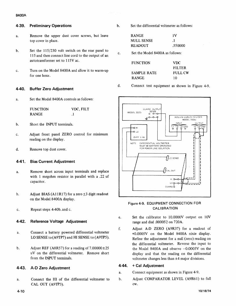
8400A
4-39. Preliminary Operations
a.
b.
c.
Remove the upper dust cover screws, but leave top cover in place.
Set the 115 /230 volt switch on the rear panel to 115 and then connect line cord to the output of an autotransformer set to 115V ac.
Turn on the Model 8400A and allow it to warm-up for one hour.
4-40. Buffer Zero Adjustment
a. Set the Model 8400A controls as follows:
b.
FUNCTION RANGE
VOC, FILT .I
Short the INPUT terminals.
c. Adjust front panel ZERO control for minimum reading on the display.
d. Remove top dust cover.
4-41. Bias Current Adjustment
a. Remove short across input terminals and replace with 1 megohm resistor in parallel with a .22 uf capacitor.
b. Adjust BIAS (Al lRl 7) for a zero ±3 digit readout on the Model 8400A display.
c. Repeat steps 4-40b. and c.
4-42. Reference Voltage Adjustment
a. Connect a battery powered differential voltmeter LO SENSE to (A9TP7) and HI SENSE to (A9TP5).
b. Adjust REF (A8R57) for a reading of?.00000±25 uV on the differential voltmeter. Remove short from the INPUT terminals.
4-43. A-0 Zero Adjustment
a.
4-10
Connect the HI of the differential voltmeter to CAL OUT (A9TP3).
b.
c.
d.
e.
f.
Set the differential voltmeter as follows:
RANGE NULL SENSE READOUT
lV .I .550000
Set the Model 8400A as follows:
FUNCTION
SAMPLE RATE RANGE
VDC FILTER FULL CW 10
Connect test equipment as shown in Figure 4-9.
!MODEL 332D I
LO
GUARD OUTPUT SENSE
0
IDIFF V Ml
!KELVIN VARLEY DIVIDER MODEL 720AI
INPUT
1.1 1.0 LO GND 0 0
I I' , I
NOTE DIFFERENTIALVOLTMETER I I I I
MUST BE BATTERY OPERATED FOR POWER LINE ISOLATION
LO SENSE
CAL OUT
I I I I I I I I I I
HI O-o--1-J'-"-=..------_,
LO 0--0-1f.k-,+--.-
GU ARD
Figure 4-9. EQUIPMENT CONNECTION FOR CALIBRATION
Set the calibrator to 10.0000V output on lOV range and dial .000052 on 720A.
Adjust A-D ZERO (A9R37) for a readout of +0.0005V on the Model 8400A nixie display. Refine the adjustment for a null (zero) reading on the differential voltmeter. Reverse the input to the Model 8400A and observe -0.0005V on the display and that the reading on the differential voltmeter changes less than ±4 major divisions.
4-44. + Cal Adjustment
a. Connect equipment as shown in Figure 4-9.
b. Adjust COMPARATOR LEVEL (A9R61) to full cw.
10/18/74
c. Dial .800052 on divider.
d. Adjust + CAL (A9Rl 7) for a readout of +8.0005 on Model 8400A display.
e. Refine the adjustment for a null (zero) on the differential voltmeter.
4-45. Ladder Cal
a. Connect equipment as shown in Figure 4-9.
b. Apply the input votlages given in Table 4-4 and perform the associated adjustments that produce the required readout on the Model 8400A and differential voltmeter.
Table 4-4. LADDER CALIBRATION
LADDER MODEL 8400A DIFF. V/M
NO. K-V Divider Adjustment READOUT READOUT
4 +.400052V LADDER 4 +4.0005V NULL (A9R45)
2 +.200052V LADDER 2 +2.0005V NULL (A9R48)
1 +.100052V LADDER 1 +1.0005V NULL (A9R50
4-46. Negative Cal Adjustment
a. Set divider to .800052.
b. Reverse input to the Model 8400A.
c. Adjust -CAL (A9R14) for a display readout of -8.0005.
d. Refine the adjustment for a null (zero) on the differential voltmeter.
4-47. Remainder Adjustment
a.
b.
c.
10/18/74
Set COMPARATOR LEVEL (A9R61) full ccw.
Connect equipment as shown in Figure 4-9.
Apply the input voltages given in Table 4-5 and perform the associated adjustments that produce the required readout on the Model 8400A and differential voltmeter.
8400A
Table 4-5. COMPARATOR LEVEL ADJUSTMENT
MODEL 8400A
DIGIT K-V Divider Adjustment READOUT DIFF. V/M
NO. SETTING READOUT
2 +.090052V 2nd Digit +0.9005 NULL Remainder (A9R58)
3 +.099052V 3rd Digit +0.9905 NULL Remainder (A9R56)
4 +.099952V - +0.9995 ±2 Major Divisions
4-48. Comparator Level Adjustment
a.
b.
c.
d.
Connect equipment as in Fignre 4-9, but do not
make the differential voltmeter connections.
Set divider to .099995.
Adjust COMPARATOR LEVEL (A9R61) so display readout alternates between +0.9999 and +1.0000.
Alternate a de input to the Model 8400A between + l.9999V and +2.0000V de and verify that the display readout corresponds.
4-49. Buffer DC Calibration
a. Apply the de input voltages given in Table 4-6 and adjust the associated control for a corresponding readout.
b.
Table 4-6. BUFFER CALIBRATION
DC INPUT MODEL 8400A
VOLTAGE RANGE ADJUSTMENT READOUT
+100.000 100 100V (A11R8) +100.000
+1000.00 1000 1000V (A11R9) +1000.00
+1.00000 1 1V (A11R36) +1.00000
+.100000 .1 0.1V (A11R38) +.100000
Disconnect test equipment and replace top cover, Calibration of the basic Model 8400A is complete. Refer to Section 6 for calibration of the options.
4-50. COMPENSATING COMPONENT SELEC-TION
4-51. The replacement of components Q5, Ul, and R22 thru R27 in the Buffer Assembly will cause a deteriation of the temperature coefficient specification. If one or all of
4-11
8400A
these components is found to be faulty the Buffer Assembly PCB must be returned to the factory for repair and recali
bration.
4-52. Active Filter
4-53. If either Ql or U2 are replaced in the Active Filter (AlO), Rl l or Rl 2 may need to be selected in order to bring the required offset correction within the range of zero control R13. This is done as follows:
a. Depress VDC and 10 buttons on Model 8400A.
b. Short the INPUT terminals of the Model 8400A.
c. Short TPl to TP2 on Active Filter PCB.
d.
e.
f.
Install jumpers across Rl 1 and Rl 2 in positions Wl and W2.
Turn instrument on by depressing POWER button.
Observe the Model 8400A readout.
g. Select the proper offset resistor using Table 4-7.
h.
Table 4-7. OFFSET CORRECTION RESISTOR SELECTION
8400A RESISTANCE JF PART NO. READOUT REQUIRED
0 - .0004 NONE --.0005 - .0012 6.81k 268417
.0013 - .0020 13.7k 236752
.0021 - .0028 21.0k 229484
.0029 - .0036 28.7k 235176
.0037 - .0044 35.7k 288480
.0045 - .0052 44.2k 271676
Install resistor in location Rl l if readout polarity is positive ( +) or R 12 if readout polarity is negative (-). Remove only the jumper wire for loca
tion used.
4-53. TROUBLESHOOTING
4-54. Introduction
4-55. The information in the following paragraphs is provided to assist in locating troubles in the basic Model 8400A. Figure 4-10 shows assembly location by reference
4-12
number and test point locations. Since this instrument is somewhat complex, it is recommended that the theory of operation in Section 3 be understood before any attempt
at troubleshooting is undertaken.
4-56. Initial Troubleshooting
4-57. Troubleshooting of the Model 8400A starts by first inspecting the instrument for improperly seated plug-in assemblies, loose wires, physically damaged parts, or other
obvious problems. The next step is then to ensure that it is being operated correctly, but still fails to meet specifications. Performance checks designed for this purpose are given in paragraphs 4-30 through 4-35.
4-58. Section Localization
4-59. To aid in troubleshooting the Model 8400A, the basic instrument can be broken down into three major sections, analog, digital, and power supply.
4-60. The analog section consists of the All Buffer and AlO Active Filter. These assemblies supply a de voltage from + 10 to -10 volts, dependent upon the polarity and value of the input, to the digital section.
4-61. The digital section is composed of the A9 A-to-D Converter, A8 Logic, A2 Range Delay, and Al4 Display assemblies. The digital section converts the de input from the analog section to a digital signal, then processes this signal through timing, storage, and display circuits for proper readout.
4-62. The power supply section consists of an Al Power Supply Assembly. This assembly supplies operating voltages to the internal circuits of both the analog and digital sections.
4-63. Power Supply
4-64. The Al Power Supply can be checked for porper operation using a de differential voltmeter and performing the voltage checks given in Table 4-8.
Table 4-8. POWER SUPPLY CHECKS
VOLTAGE DC VOLTS
TEST POINTS
V/M Lo V/MHi NOMINAL LIMITS ADJUSTMENT
A1TP4 A1TP2 +18V ±10mV A1R11
A1TP4 A1TP3 -18V ±375 mV NONE
A1TP4 A1TP5 +5V +.15V Remove R17 to increase
A1TP4 A1TP1 +200V ±5V NONE

8400A
A1 A2TP3TP2 TP1 TP 1 TP2 TP3 A8 A9
TP7
TP6
TP5
A11
TP1
TP4
TP3
TP5 TP2
TP1 A10
TP5
TP4
TP4 TP3
TP3 TP2 TP2 TP1
TP1
Figure 4-10. ASSEMBLY AND TEST POINT LOCATIONS
4-13

8400A
4-65. Analog Section
4-66. To determine if a trouble exists in the analog sec-tion, use the following checks:
a. Connect a battery powered differential voltmeter LO to A10TP4 and HI to AlOTP3.
b. Depress VDC and 10 switches on Model 8400A.
c. Turn on the Model 8400A and apply + 1 OV de to INPUT terminals. The differential voltmeter should read - lOV.
NOTE!
The differential voltmeter should read -lOV for fell scale inputs on the 10, 100, and 1000 volt ranges, and +lOV for fell-scale inputs on the .1 and 1 volt ranges. For inputs less than fell-scale on any range, the differential voltmeter should read proportionately less.
(Example: +IOV input on lOOV range, the differential voltmeter will read -1 V).
------FAULT ANALYSIS------.
IF VOLTMETER READINGS DO NOT COR
RESPOND TO INPUT VOLTAGES, THE TROUBLE EXISTS IN THE ANALOG SECTION. IF VOLTMETER READINGS DO CORRESPOND TO INPUT VOLTAGES, THE TROUBLE EXISTS IN THE DIGITAL SECTION.
4-6 7. BUFFER CHECKS.
4-68. Overload Check.
a. Connect differential voltmeter HI to Kl pin 14 and LO to the Model 8400A HI (red) INPUT terminal.
b. Depress the l, VDC, FILI buttons and set SAMPLE RA TE full cw.
c. Apply +3V ±1% to INPUT terminals of 8400A and observe readout of +1.19999. The differential voltmeter should read -.SV ±.25V.
4-14
------FAULT ANALYSIS------,
IF READINGS DO NOT CORRESPOND, THE PROBABLE CAUSE IS IN THE OVERLOAD CIRCUITRY. THE AMPLIFIER SECTION MAY BE A SECONDARY CAUSE.
4-69. Zero Check.
a. Depress .1 and VDC buttons on Model 8400A.
b. Short the INPUT terminals on front panel.
c. Readout Zero Volts on Readout display.
d. Adjust front panel DC Zero control so readout varies from +.000030 to -.000030.
------FAULT ANALYSIS-------.
IF DC ZERO CONTROL WILL NOT SWING THROUGH ABSOLUTE ZERO, ADJUST· MENT OF COURSE DC ZERO (A 11 R28) IS INDICATED. IF THIS IS NECESSARY, THE
AMPLIFIER SECTION OF THE BUFFER COULD BE FAULTY.
NOTE!
The BUFFER assembly must be returned to factory for replacement of faulty parts within the amplifier circuitry. Refer to paragraph 4-51 for critical components.
4-70. Gain Check.
a. Depress 10 button on Model 8400A.
b.
c.
d.
e.
f.
Connect a battery powered differential voltmeter as follows:
HI to INPUT HI on Model 8400A. LO to Al 1TP2
Apply -12.SV ±.SV to INPUT terminals of Model 8400A.
Readout on Model 8400A should be -11.9999.
Adjust the differential voltmeter to obtain measured value (null).
Reverse the polarity of the input voltage and observe the following:

1.
2.
Model 8400A readout is +11.9999.
Differential voltmeter reading changed less than +25 µV.
------FAULT ANALYSIS-------
IF BUFFER CHECKS ARE OK, ANALOG PROBLEM CAN EXISTS IN ACTIVE FILTER
CIRCUITRY.
4-71. ACTIVE FILTER CHECKS.
4-72. Gain Checks.
NOTE!
Remove Remote Control Unit if Model 8400A is so equipped.
a. Depress REMOTE button on Model 8400A.
b. Connect battery powered differential voltmeter LO to AlOTP5 and HI to AlOTP3.
c. Adjust differential voltmeter to obtain measured value (null).
d. Apply +lOV de ±lV between AlOTP4 (common) and AlOTP5. The differential voltmeter indication should not change more than 100 µV.
e. Reverse polarity of input voltage and note that differential voltmeter indication should not change more than 100 µV.
4-73. AC Rejection.
a. Depress VDC, FILT, 10 buttons.
b.
c.
Apply a 3V rms ± 1 %, 60 Hz signal to the INPUT terminals of Model 8400A.
Adjust SAMPLE RATE control so the readout changes about twice a second.
d. The Model 8400A readout should be less than 20 digits.
4-74. Digital Section
4-75. The digital section may be divided into.a number of somewhat independent sections for trouble analysis.
8400A
These digital sections and their locations are as follows:
LOCATION
Al4 - Display
DIGIT AL SECTIONS
Range Counter Sample Command Oscillator Readout Tubes and Controls
A9 - A-to-D Converter
AID Amplifier Sample and Hold Analog Comparator Ladder {Primary and Secondary) Display Storage
A8 - Logic Master Clock cco Analog Cycle Control Display Storage Control 6-State Shift Register 16-State Binary Counter
4-76. Generally troubleshooting the digital section is more difficult than the analog section; therefore, troubleshooting guides {Figure 4-11 and 4-12) are important aids for localizing troubles to sections.
NOTE!
1he storage cycle can be bypassed if there is a suspicion that the storage circuitry is faulty. A FAULTY storage cycle is usually seen as flashing digits. By jumpering Al1P5 (+5V) to AJ41P2 (M), the Model 8400A is placed into a continuous measurement mode.
4-77. Figures 4-13 thru 4-16 are idealized waveforms from significant locations showing relationship of each waveform to the others and to the measure period. Analysis of these waveforms and a comparison to waveforms present at the same points will assist in localizing troubles. All waveforms are as shown when Model 8400A is placed in the continuous measurement condition.
------FAULT ANALYSIS-------.
IF, AFTER PLACING THE MODEL 8400A
INTO THE CONTINUOUS MEASUREMENT CONDITION, THE READOUT IS CORRECT, THE FAULT LIES IN THE STORAGE CIRCUITRY. IF READOUT IS STILL INCORRECT THE FAULT LIES ELSEWHERE.
4-78. Figures 4-17 thru 4-19 show waveforms that are present at A9TP2 with Model 8400A in continuous measurement condition. Analysis of these waveforms to those present under trouble conditions will assist in troubleshooting the digital section.
4-15
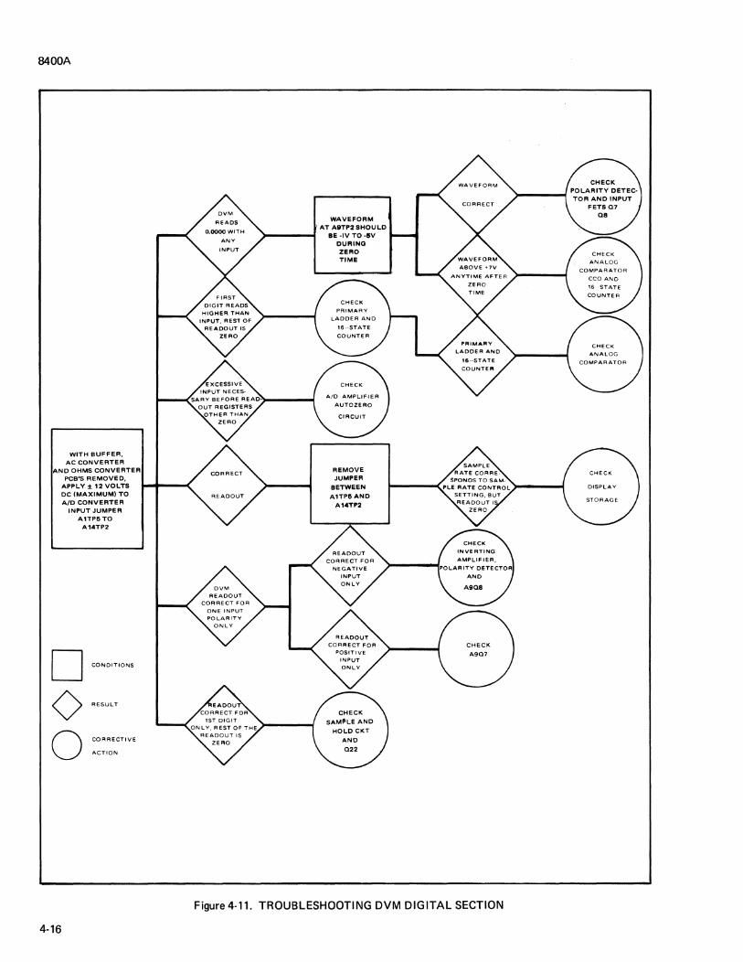
8400A
WITH BUFFER, AC CONVERTER
AND OHMS CONVERTER PCB'S REMOVED,
APPLY.± 12 VOLTS DC (MAXIMUM) TO AID CONVERTER
INPUT JUMPER A1TP6TO
A14TP2
D CONDITIONS
() RESULT
0 CORRECTIVE
ACTION
4-16
WAVEFORM AT A9TP2SHOULD
BE ·IV TO ·llV DURING ZERO
REMOVE JUMPER
BETWEEN A1TPllAND
A14TP2
Figure4-11. TROUBLESHOOTING DVM DIGITAL SECTION
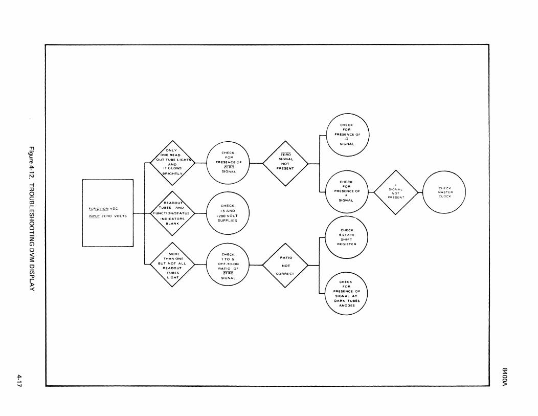
"Tl cE" c: ., Cl>
f" .... !')
-I :::0 0 c CD r m Cf)
::i:: 0 0 ::! 2 G)
0 < s: 0 Cf) "'O r )> -<
INPUT 2E AO VOL TS

8400A
~ZERO ·~ GATE 11
STORE INP.l
GATE 2
GATES 1, 22
STORE OUT
GATE4-----
A "'4
n I
av-
-18V I
B ·~ c •14
I n I
4.5µs _.j r-I
NOTE: LOGIC 1 = OVDC LOGIC 0 = -18VDC
D
Figure 4-13. A/D CONVERTER CONTROLS
!+--A .. ,4 B •14 c .. , ... D
A806
A807
A8Q8
A8010
4-18
-1~·-~ I -18V
NOTE: LOGIC 1 = OVDC LOGIC 0 = -18VDC
I
I I
I
Figure 4-14. ANALOG STORAGE CONTROL
•14 E~
I A8017
I A8012
A8016
A8015
A8013
.. , ... E----+!
S1
S2
S3
S4
.__ __ SS
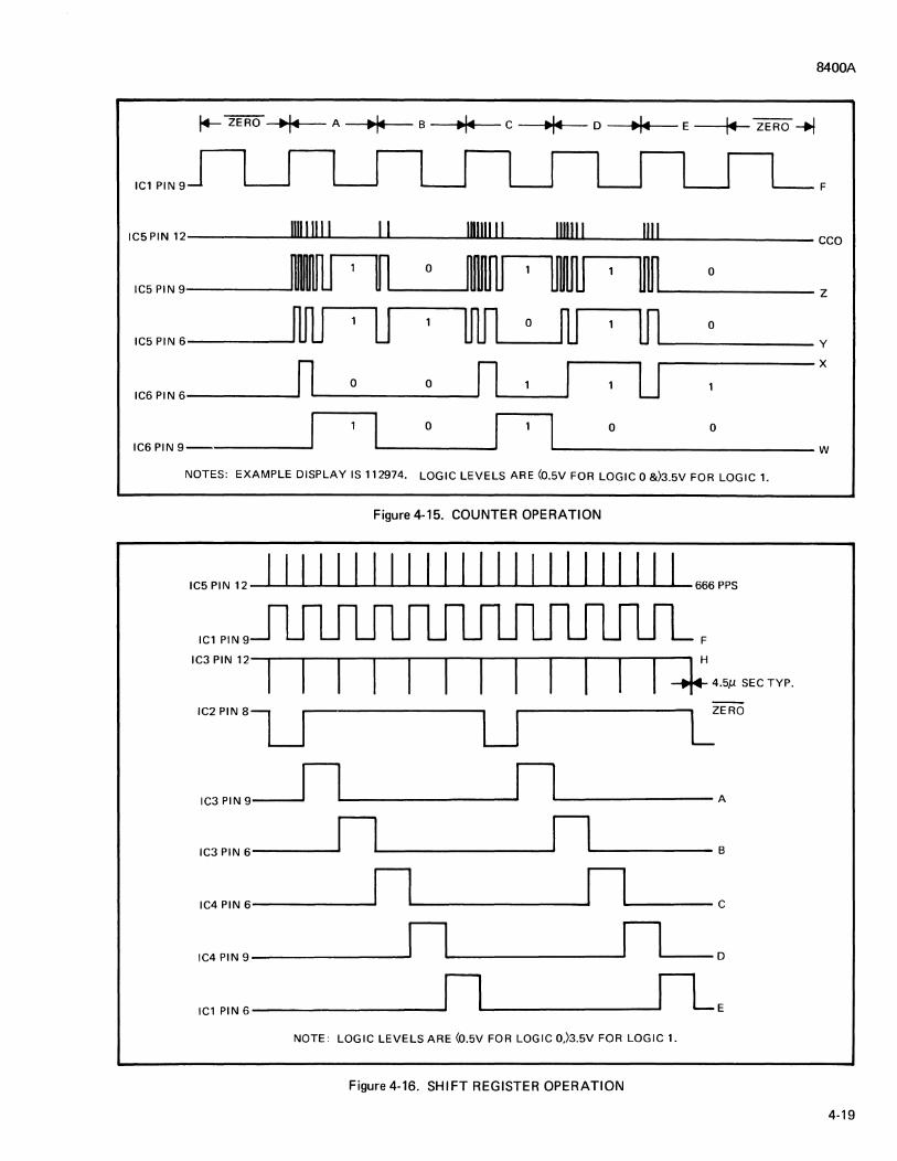
8400A
A -~llo~'--- B ---tlloMI~..._- C _ _..,.._,4_ D --4111o,..l4i----E --~-ZERO -.i
IC1PIN9 F
IC5 PIN 12 111111111 11 IUllll 11 1111111 Ill I cco
IU ~ 0 l1J lMIU 001 0
IC5 PIN 9 z
ruu u mn 0 ~ lJl 0
IC5 PIN 6 y
n n I lJ x
0 0 IC6 PIN 6
I 0 I 0 0
IC6PIN9 w
NOTES: EXAMPLE DISPLAY IS 112974. LOGIC LEVELS ARE (0.5V FOR LOGIC 0 &)3.5V FOR LOGIC 1.
Figure 4-15. COUNTER OPERATION
IC5PIN12 I I I I I I I I I I I I I I I I I I I 11 11 I 666 PPS
IC1 PIN 9 F
ic3PIN 12-1 ~I -1 -1 ------, ------, --r-1 -r---1 -r--1 -r--1 ~I r-----11 +4.5µ sEcTvP.
IC2PIN8LJ LJ IC3 PIN 9--......JnL.----------'nL--------- A
IC3 PIN 6------'n nr.., _______ B
IC4 PIN 6---------'n nr.., _____ c
IC4 PIN 9----------""n nr.., ___ D
IC1 PIN 6-------------'n n_ E
NOTE: LOGIC LEVELS ARE (0.5V FOR LOGIC 0)3.5V FOR LOGIC 1.
Figure 4-16. SHIFT REGISTER OPERATION
4-19

8400A
4-20
--+--------------------------------------5 V/CM -VERT 2 MSEC/CM - H OR Z
OVOLTS--------
PERIOD
A c
--+-------------------OVINPUT FILT, VDC, 10 DEPRESSED
------OVOLTS
D
Figure 4-17. A9TP2 MEASUREMENT
-+-------------------------------------SCOPE 5 V/CM - VERT 2 MSEC/CM - H OR Z
(3.524)
~REMAINDER~
6.3524V de INPUT FILT, VDC, 10 DEPRESSED MEASUREMENT
(5.24)
12.4)
Figure 4-18. A9TP2
T (4.0) 7 VOLTS
NOTES:
1. NOTICE THE NUMBER OF COUNTS ON EACH PULSE.
2. TIME BETWEEN EACH COUNT SHOULD BE LARGER THAN PRECEEDING TIME.
3. PERIOD E REMAINDER WILL BE UNSTABLE DUE TO AMPLIFIER NOISE.

. 99999V de INPUT Fl LT, voe. 1 OEPRESSED MEASUREMENT CYCLE
Figure 4-19. A9TP2
SCOPE 5 V /CM - VE RT 2 MSEC/CM - HOR Z
NOTES:
1. 9 COUNTS ON EACH PULSE.
2. EACH COUNT HAPPENS ON THE SAME LEVEL. (EX lST LEVEL COUNT ON EACH PULSE) .
8400A
4-21


8400A
Section 5
List of Replaceable Parts
5-1. INTRODUCTION
5-2. This section contains an illustrated parts breakdown list of the instrument and a Cross Reference List of FLUKE stock numbers to original MANUFACTIJRERS' part numbers. It also lists recommended spare parts and contains part ordering information. The starting page number of each major listing is given in the Table of
Contents.
5-3. The parts list shows the location of all assemblies and the replaceable components. Major assemblies are identified by a designation beginning with the letter A followed by a number (e.g., Al etc). Subassemblies are identified in the same manner; however, the parent assembly designator precedes this designator (e.g., AIAI etc.). Electrical components are identified by their schematic diagram designator and listed hardware parts are identified by the FLUKE stock number. All listed components are described, and the FLUKE stock number is given. The original MANUFACTIJRER'S part number for each listed item is given in the Cross Reference List at the rear of this
section.
5-4. PARTS LIST COLUMN DESCRIPTIONS
a. The REF DESIG column indexes the item description to the associated illustration. In general the reference designations are listed under each assembly in alpha-numeric order. Subassemblies of minor proportions are sometimes listed with the assembly of which they are a part. In this case, the reference designations may appear out of order.
b.
c.
d.
e.
The DESCRIPTION column describes the salient characteristics of the component. Indention of the description indicates the relationship to other assemblies, components, etc. In many cases it is necessary to abbreviate in this column. For ab· breviations and symbols used, refer to Appendix B located at the rear of the manual.
The six-digit part number, by which the item is identified at the John Fluke Mfg. Co., Inc. is listed in the STOCK NO. column. Use this number when ordering parts from the factory or authorized representatives. In the case where a flag note is used, special ordering is required. Flag note explanations are located as close as possible to the flag note.
The TOT QTY column lists the total quantity of the item used in each particular assembly. This quantity reflects only the latest lJse Code. Second and subsequent listings of the same item are referenced to the first listing with the abbreviation REF.
Entries in the REC QTY column indicate the recommended number of spare parts necessary to support one to five instruments for a period of two years. This list presumes an availability of common electronic parts at the maintenance site. For maintenance for one year or more at an isolated site, it is recommended that at least one of each assembly in the instrument be stocked. In
5-1
8400A
f.
5-5.
a.
b.
c.
5-2
the case of optional subassemblies, plug-ins, etc. that are not always part of the instrument, or are deviations from the basic instrument model, the REC QTY column lists the recommended quantity of the item in that particular assembly.
The USE CODE column identifies certain parts which have been added, deleted or modified during the production of the instrument. Each part for which a Use Code has been assigned may be identified with a particular instrument serial number by consulting the Serial Effectivity List, paragraph 5-9. Sometimes when a part is changed, the new part can and should be used as a replacement for the original part.
MANUFACTURERS' ENCE LIST COLUMN
CROSS REFER-DESCRIPTIONS
The six-digit part number, by which the item is identified at the John Fluke Mfg. Co., Inc. is listed in the FLUKE STOCK NO. column. Use this number when ordering parts from the factory or authorized representatives.
The Federal Supply Code for the item manufacturer is listed in the MFG column. An abbreviated list of Federal Supply Codes is included in Appendix A.
The part number which uniquely identifies the item to the original manufacturer is listed in the MFG PART NO. column. If a component must be ordered by description, the type number is listed.
5-6. HOW TO OBTAIN PARTS
5-7. Standard components have been used whenever possible. Standard components may be ordered directly from the manufacturer by using the manufacturer's part number, or parts may be ordered from the John Fluke Mfg. Co., Inc. factory or authorized representative by using the FLUKE stock number. In the event the part you order has been replaced by a new or improved part, the replacement will be accompanied by an explanatory note and installation instructions, if necessary.
5-8. You can insure prompt and efficient handling of your order to the John Fluke Mfg. Co., Inc. if you include the following infonnation:
a. Quantity.
b. FLUKE Stock Number.
c. Description.
d. Reference Designation.
e. Instrument model and serial number.
Example: 2 each, 215897, Transistor, 2N4126
A2A1Ql & Q2 for 645A, S/N 123.
If you must order structural parts not listed in the parts list, describe the part as completely as possible. A sketch of the part, showing its location to other parts of the instrument is helpful.

5-9. SERIAL NUMBER EFFECTIVITY
5-10. A Use Code column is provided to identify certain parts that have been added, deleted or modified during production of the Model 8400A. Each part for which a use code has been assigned may be identified with a particular instrument serial number by consulting the Use Code Effectivity List below. All parts with no code are used on all instruments with serial numbers above 123.
USE CODE SERIAL NUMBER EFFECTIVITY
A 123 thru 148.
B 149 and on.
c 187 and on.
D 198 and on.
E 123 thru 264.
F 265 and on.
G 123 thru 267.
H 268 and on.
123 thru 265.
J 266 and on.
K 378 and on.
L 330 and on.
M 123 thru 377.
N 123 thru 332.
0 333 and on.
p 123 thru 632.
Q 633 and on.
R 123 thru 272.
s 273 and on.
T 554 and on.
u 123 thru 553.
v 76400 and on.
10/18/74
8400A
5-3

8400A
REF MFG MFG DESIG FLUKE FED PART NO. TOT REC USE OR DESCRIPTION STOCK SPLY OR QTY QTY COE ITEM NO. COE TYPE NO.
8400A DIGITAL VOLTMETER Figure 5-1
Al Power Supply (Figure 5-2) 288159 1
A2 Range Delay (Figure 5-3) 288209 1
A3 DC External Reference (See Section 6, -05 Option not supplied with standard 8400) [1> 1
A4 AC External Reference (See Section 6, -06 Option not supplied with standard 8400) [I> 1
AS Remote Control (See Section 6, -04 Option not supplied with standard 8400) [t> 1
A6 Data Output No. 2 (See Section 6, -03 Option not supplied with standard 8400) [L>- 1
A7 Data Output No. 1 (See Section 6, -03 Option [t::>-not supplied with standard 8400) 1
A8 Logic (Figure 54) [t::> 1
A9 AD Converter (Figure 5-5) [l:::> 1
AlO Active Filter (Figure 5-6) [L:::::=.. 1
All Buffer (Figure 5-7) 288191 1
Al2 Ohms Converter (See Section 6, -02 Option not supplied with standard 8400) [t::>- 1
A13 AC Converter (See Section 6, -01 Option not supplied with standard 8400) IT> 1
Al4 Display (Figure 5-8) 288167 1
A22 True RMS converter (See Section 6, -09 Option not supplied with standard 8400) [1> 1
Cl Cap, cer, fixed 47 pf ±10% 282145 1
J25, Binding post, red, Hi 275552 2 J27
J26, Binding post, black, Lo 275560 2 J28
J30, Jack, teflon, ins (Mounted on Tl) 295287 2 J31
J32 Binding post, blue, guard 275578 1
54 10/18/74

8400A
REF MFG DESIG FLUKE MFG
OR DESCRIPTION STOCK FED PART NO. TOT REC USE ITEM NO. SPLY OR QTY QTY COE
NO. COE TYPE
RI, R2 Res, ww, SOK, ±25% 307298 2
R3 Res, comp, lOM ±10%, 71w 108I42 I c SI Switch, power (for push button, see below) 29I526 I
Button, push, green 268862 I
Cover, top, outer 311746 I
Cover, top guard 346I63 I
Cover, access 2977I3 I
Cover, bottom 298554 I
Foot 292870 4
Knob, black I90249 I
Lens 297903 I
Line, cord and plug 284I74 I
Shorting Link I90728 3
Terminal, double 30I382 4
Terminal, single 301390 5
Terminal strip, black 305136 4
Terminal strip, ins, light grey 297846 6
[[::::::>- Order by model and option number
~ A8 and A9 must be gurchased as a set Stock number 3034 l
corvt..~.r t'l[ufA{__ Datt I 5 .zql..ZYI
10/18/74 5-5

8400A
REF DESIG FLUKE MFG MFG
OR DESCRIPTION STOCK FED PART NO. TOT REC USE
ITEM NO. SPLY OR QTY QTY COE
NO. COE TYPE
REAR PANEL ASSEMBLY
Figure 5-1
Pl Connector, AC receptacle 284166 1
Fl Fuse, AGC *-A fast-blo 153858 1
XFl Fuse Holder 295741 1
Panel, rear (includes slide switch, stock no. 226274) 297645 1
Tl Transformer, power 365171 1
5-6 10/18/74

8400A
Figure 5-1. MODEL 8400A DIGITAL VOLTMETER
10/18/74 5-7

8400A
REF MFG MFG DESIG FLUKE
OR DESCRIPTION STOCK FED PART NO. TOT REC USE ITEM NO. SPLY OR QTY QTY COE NO. COE TYPE
Al POWER SUPPLY 2881S9 REF Figure 5-2
Cl Cap, elect, 8 uf +S0/-10%, 3SOV 27S792 1
C2, Cap, elect, 2SO uf +S0/-10%, 40V 178616 2 cs
C3, Cap, mica, 33 pf ±.S%, SOOV 160317 2 C7
C4, Cap, elect, SO uf +S0/-10%, 2SV 168823 2 C6
C8 Cap, elect, 7100 uf +7S/-10%, lOV 29S196 1
CRl thru Diode, silicon, 1 amp, 600 piv 112383 4 CR4
CRS thru CR8,
Diode, silicon, 1 amp, 100 piv 116111 8 CRlO thru CR13
CR9 Diode, zener, 12V 2490S2 1
Ql, Tstr, silicon, NPN 218Sll 2 Q2
Q3, Tstr, silicon, NPN 1S03S9 Q8 2
Q4 Not used 1S03S9 2
QS Tstr, silicon, PNP 269076 -1
Q6 Tstr, silicon, NPN 288381 1
Q7 Tstr, silicon, NPN 218396 1
Rl Res, comp, S 10 ±.S%, 71.w 1089S 1 1
R2 Res, comp, 68k ±.S%, 74w 148171 1
R3 Res, met flm, 383k±.1%, l/8w 288498 1
R4, Res, met flm, 40.2k ±.1%, 1/8w 23S333 2 RlS
RS, Res, comp, S 1 ±.S%, 71.w 144717 2 R8
l
5-8 10/18/74
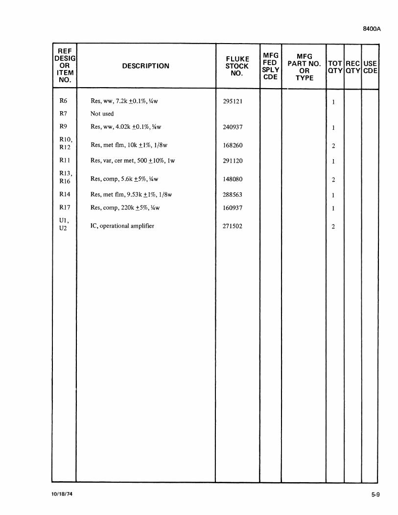
8400A
REF DESIG FLUKE MFG MFG
OR DESCRIPTION STOCK FED PART NO. TOT REC USE ITEM NO. SPLY OR QTY QTY COE NO. COE TYPE
R6 Res, ww, 7.2k±0.1%,%w 295121 I
R7 Not used
R9 Res, ww, 4.02k ±0.1%, %w 240937 I
RIO, Res, met flm, IOk ±1%, l/8w Rl2 168260 2
RI I Res, var, cermet, 500 ±10%, lw 291120 I
Rl3, Rl6 Res, comp, 5.6k ±5%, %w 148080 2
Rl4 Res, met flm, 9.53k ±1%, I/8w 288563 I
RI7 Res, comp, 220k ±5%, %w 160937 I
Ul, U2 IC, operational amplifier 271502 2
10/18/74 5-9

8400A
Figure 5-2. POWER SUPPLY PCB ASSEMBLY
5-10 10/18/74

8400A
REF MFG DESIG FLUKE r.:lFG
OR DESCRIPTION STOCK FED PART NO. TOT REC USE
ITEM NO. SPLY OR QTY QTY COE
NO. COE TYPE
A2 RANGE DELAY 288209 REF
Figure 5-3
Cl, Cap, cer, 0.02S uf ±20%, lOOV C3 16843S 2
C2, Cap, Ta, 3.3 uf ±S%, 20V C6 271320 2
C4 Cap, mica, 0.01 uf ±1%, 300V 1S2470 I
cs Cap, elect, 200 uf +S0/-10%, lOV 236935 I
C7 Cap, cer, 2200 pf, ±10%, SOOY 26842S I Q
C8 Cap, cer, .01 uf,±20%, lOOV 1491S3 I Q
CRI, CR3,
Diode, silicon ISO mA CR9, 203323 4 E
CRI I
CRI, CR3,
Diode, silicon, ISO mA CR9, 203323 s F
CRII CR16
CR2, CR6, CR7, Diode, germanium, 80 mA, 100 piv 149187 s E CR8, CRIC
CR2, CR6, CR7, CR8,
Diode, germanium, 80 mA, 100 piv CRIC 149187 9 F
CR12 thru CRIS
CR4, Diode, fast switching germanium, SO piv CRS 180SOS 2
QI, Tstr, silicon, NPN Q2 168708 2
Q3 Tstr, silicon, NPN 218396 I E
10/18/74 5-11

8400A
REF MFG MFG DESIG FLUKE
OR DESCRIPTION STOCK FED PART NO. TOT REC USE ITEM NO. SPLY OR QTY QTY COE NO. COE TYPE
Q3,QS Tstr, silicon, NPN 218396 2 F
Q4 Tstr, silicon, uni junction 268110 1
Rl,R6, Res, comp, 220 ±5%, %w 147959 RlS 3
R2 Res, comp, 22k ±5%, %w 148130 1
R3,R7 Res, comp, 4.7k ±5%, %w 148072 2
R4,R17 Res, comp, 27k ±5%, %w 148148 2
RS Res, comp, 5 lk ±5%, %w 193334 l
R8 Res, met fun, 27.4k±1%, 1/8w 241471 1
R9 Res, met fun, 15.4k ±1%, 1/8w 261651 1
RIO Res, comp, 47k ±5%, %w 148163 1
Rl l Res, comp, 1 Ok ±5%, %w 148106 1 E
Rll, Res, comp, lOk ±5%, %w 148106 R19 2 F
R12 Res, met fun, lOk ±1 %, 1/8w 168260 1
R13 Res, met flm, 36.Sk ±1%, 1/8w 235309 1
R14 Res, met flm, 21k ±0.5%, 1/8w 229484 1 E
Res, met fun, 16.9k±1%, 1/8w 267146 1 F
R16 Res, comp, 5 .lk ±5%, %w 193342 1
R18 Res, var, cermet, lOk ±10%, ~w 285171 1 F
U1 IC, DTL, Hex Inverter 268367 1
U2 IC, DTL, Triple 3-Input Nand Gate 266312 1
U3 IC, DTL, dual 4-Input Nand 268383 1
Socket, IC, 14 contact, Ul, U2, U3 276527 3
5-12 10/18/74

8400A
Figure 5-3. RANGE DELAY PCB ASSEMBLY
10/18/74 5-13
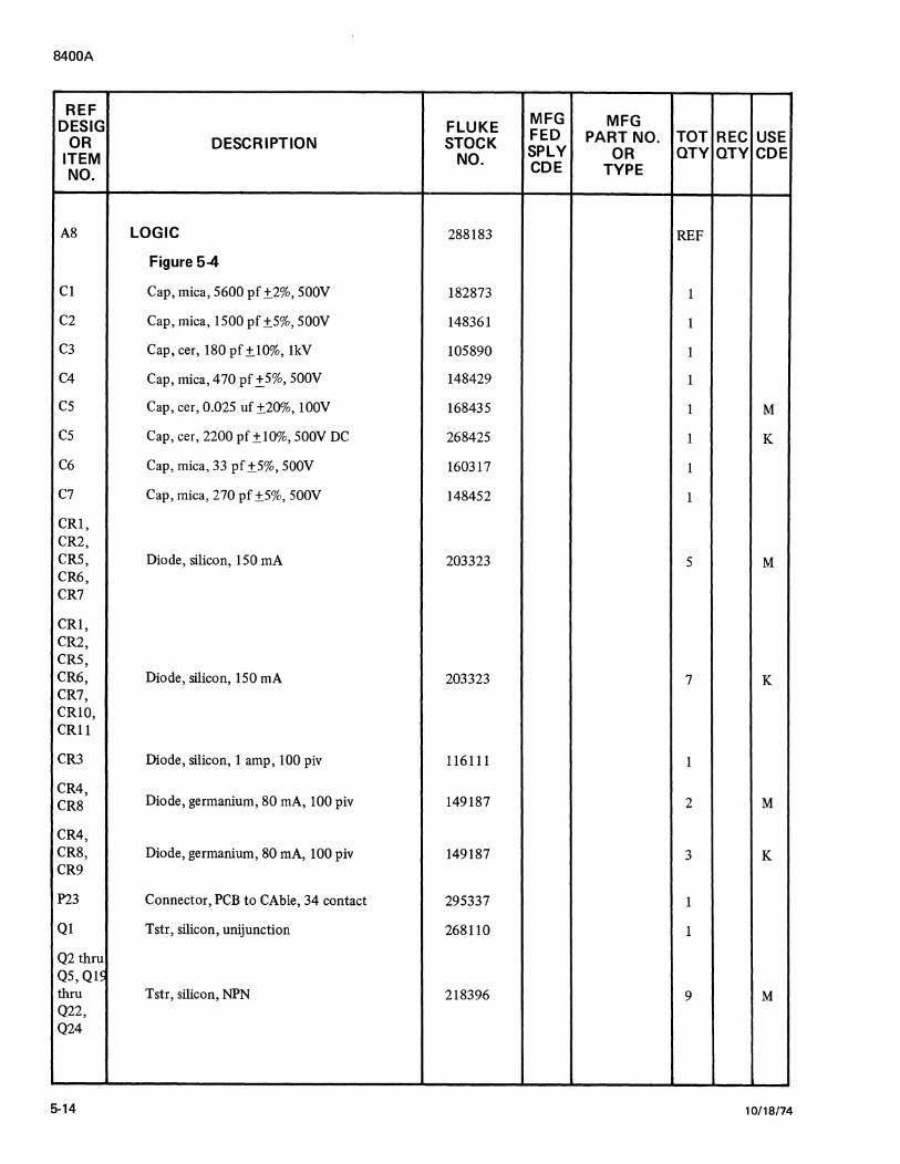
8400A
REF MFG MFG DESIG FLUKE FED PART NO. TOT REC USE OR DESCRIPTION STOCK ITEM NO. SPLY OR QTY QTY COE NO. COE TYPE
A8 LOGIC 288183 REF
Figure 5-4
Cl Cap, mica, S600 pf ±.2%, SOOY 182873 1
C2 Cap, mica, lSOO pf ±.S%, SOOY 148361 1
C3 Cap, cer, 180 pf ±.10%, lkY 10S890 1
C4 Cap, mica, 470 pf ±_S%, SOOY 148429 1
cs Cap, cer, 0.02S uf ±.20%, lOOY 16843S 1 M
cs Cap, cer, 2200 pf ±.10%, SOOY DC 26842S 1 K
C6 Cap, mica, 33 pf ±.S%, SOOY 160317 1
C7 Cap, mica, 270 pf ±.S%, SOOY 1484S2 1
CRl, CR2, CRS, Diode, silicon, ISO mA 203323 s M CR6, CR7
CRl, CR2, CRS, CR6, Diode, silicon, ISO mA 203323 7 K CR7, CRlO, CRll
CR3 Diode, silicon, 1 amp, 100 piv 116111 1
CR4, Diode, germanium, 80 mA, 100 piv 149187 2 M CR8
CR4, CR8, Diode, germanium, 80 mA, 100 piv 149187 3 K CR9
P23 Connector, PCB to CAble, 34 contact 29S337 1
QI Tstr, silicon, unijunction 268110 1
Q2 thru Qs,Qg thru Tstr, silicon, NPN 218396 9 M Q22, Q24
5-14 10/18/74
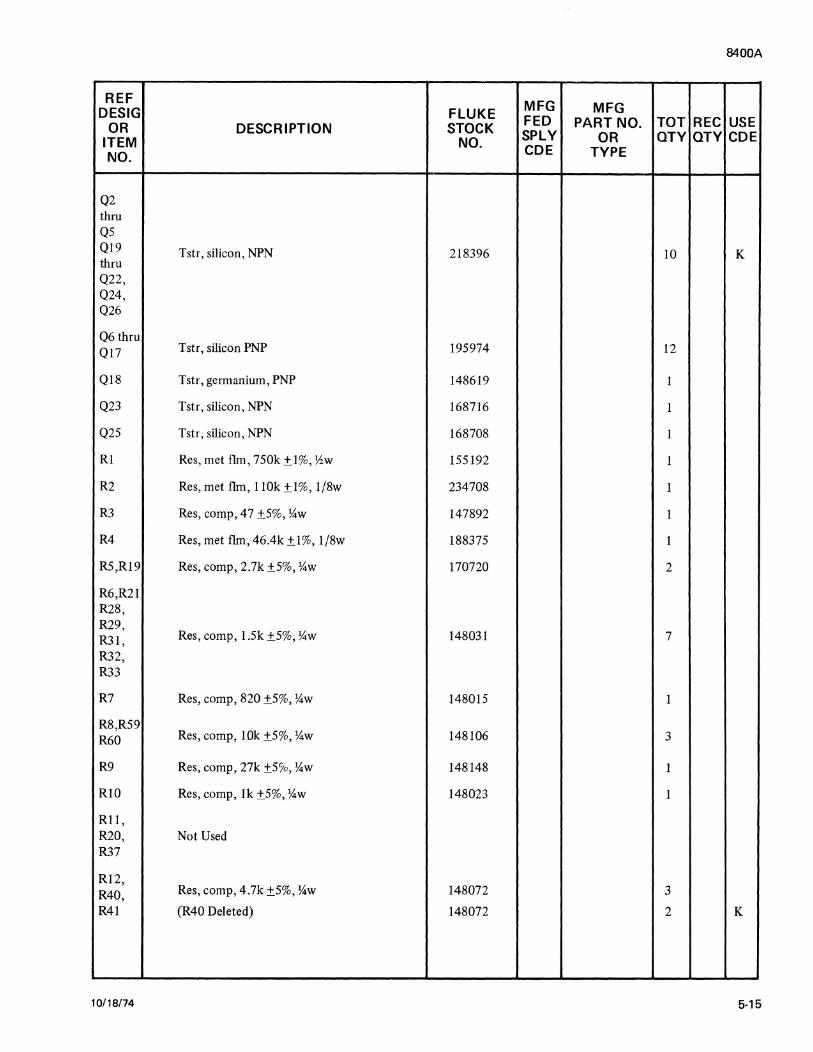
8400A
REF MFG MFG DESIG FLUKE OR DESCRIPTION STOCK FED PART NO. TOT REC USE
ITEM NO. SPLY OR QTY QTY CDE NO. CDE TYPE
Q2 thru Q5 QI9 Tstr, silicon, NPN 218396 IO K thru Q22, Q24, Q26
Q6 thru Ql7 Tstr, silicon PNP 195974 12
Ql8 Tstr, germanium, PNP 148619 I
Q23 Tstr, silicon, NPN 168716 I
Q25 Tstr, silicon, NPN 168708 I
RI Res, met fun, 750k ±1%, 7lw 155192 I
R2 Res, met fun, I !Ok ±1%, l/8w 234708 I
R3 Res, comp, 47 ±5%, %w 147892 I
R4 Res, met fun,46.4k±l%, l/8w 188375 I
R5,Rl9 Res, comp, 2.7k ±5%, %w 170720 2
R6,R21 R28, R29,
Res, comp, l .Sk ±5%, %w R31, 148031 7
R32, R33
R7 Res, comp, 820 ±5%, %w 148015 I
R8,R59 Res, comp, !Ok ±5%, %w R60 148106 3
R9 Res, comp, 27k ±5%, %w 148148 1
RIO Res, comp, lk ±5%, %w 148023 1
Rll, R20, Not Used R37
Rl2, Res, comp, 4.7k ±5%, %w 148072 3 R40,
R41 (R40 Deleted) 148072 2 K
10/18/74 5-15

8400A
REF MFG MFG DESIG FLUKE OR DESCRIPTION STOCK FED PART NO. TOT REC USE
ITEM NO. SPLY OR QTY QTY COE NO. COE TYPE
R13, R25,
Res, comp, 8.2k ±5%, %w 160796 R26, 4
R27
R14 thru Res, comp, 5 lk ±5%, %w 193334 5 R18 (Rl 7 Deleted) 193334 4 K
R22, Res, comp, 2.2k ±5%, %w 148049 R23 2
R24, Res, comp, 1.8k ±5%, %w R64 175042 2
R30 Res, comp, 680 ±5%, %w 148007 1
R34, R35,
Res, comp, 22k ±5%, %w 148130 R36, 5
R38, R39
R42 Res, comp, 33k ±5%, %w 148155 1
R43 Res, comp, 47k ±5%, %w 148163 1 M
R43, R66 Res, comp, 47k ±5%, %w 148163 2 K
R43, R66, Res, comp, 47k ±5%, %w 148163 3 v R67
R44, R50, Res, comp, 220k ±5%, Y<iw 160937 3 R52
R45, R46, R48,
Res, comp, l lk ±5%, %w R49, 221580 6
R51, R65
R47 Res, comp, 39k ±5%, Y<iw 188466 1
R53 Res, met flrn, 182k ±1%, 1/8w 241091 1
R54 Res, met flrn, 3.74k±1%, 1/8w, T9 260547 1
R57 Res, var, cermet, 20±20%,1hw 261180 1
R58 Res, ww, 14k±0.1%, Y<iw 275321 1
5-16 10/18/74
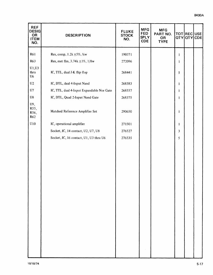
8400A
REF MFG MFG DESIG FLUKE
OR DESCRIPTION STOCK FED PART NO. TOT REC USE ITEM NO. SPLY OR QTY QTY COE NO. COE TYPE
R61 Res, comp, 1.2k ±5%, ~w 190371 1
R63 Res, met fltn, 3.74k ±1%, 1/8w 272096 1
Ul,U3 thru IC, TTL, dual J-K flip flop 268441 5 U6
U2 IC, DTL, dual 4-Input Nand 268383 1
U7 IC, TTL, dual 4-Input Expandable Nor Gate 268557 1
U8 IC, DTL, Quad 2-Input Nand Gate 268375 1
U9, R55,
Matched Reference Amplifier Set 290650 R56, 1
R62
UlO IC, operational amplifier 271501 1
Socket, IC, 14 contact, U2, U7, U8 276527 3
Socket, IC, 16 contact, Ul, U3 thru U6 276535 5
10/18/74 5-17
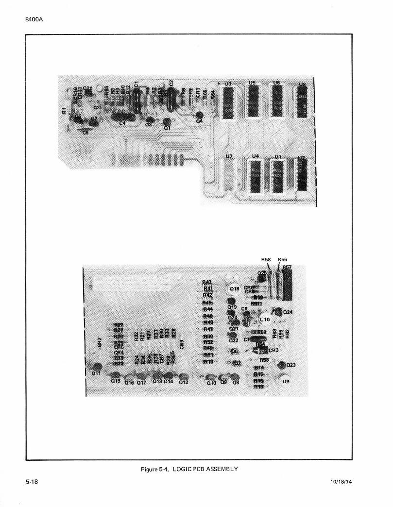
8400A
R58 R56
Figure 5-4. LOGIC PCB ASSEMBLY
5-18 10/18/74
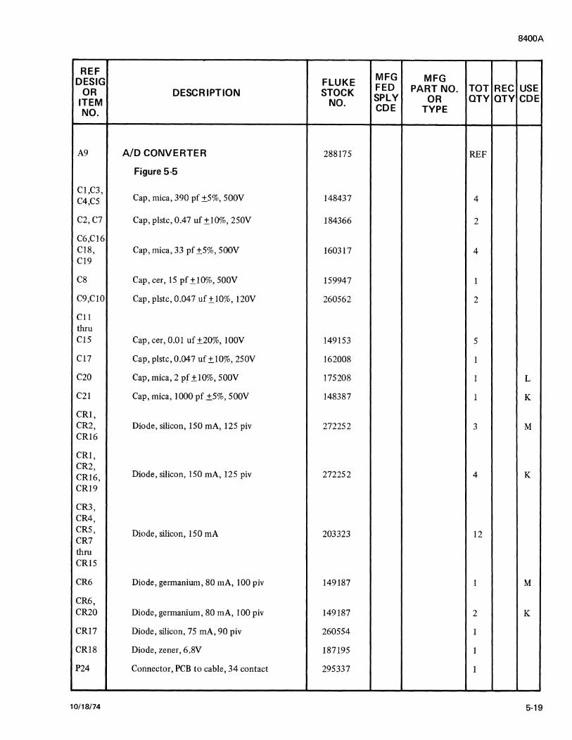
8400A
REF MFG MFG DESIG FLUKE
OR DESCRIPTION STOCK FED PART NO. TOT REC USE
ITEM NO. SPLY OR QTY QTY COE
NO. COE TYPE
A9 A/D CONVERTER 28817S REF
Figure 5-5
Cl,C3, Cap, mica, 390 pf ±S%, SOOY 148437 C4,CS 4
C2,C7 Cap, piste, 0.47 uf ±10%, 2SOY 184366 2
C6,CI6 CI8, Cap, mica, 33 pf ±S%, SOOY 160317 4 CI9
C8 Cap, cer, IS pf ±10%, SOOY IS9947 I
C9,C10 Cap, piste, 0.047 uf ±10%, 120Y 260S62 2
Cl I thru CIS Cap, cer, 0.01 uf ±20%, IOOV 149IS3 s CI7 Cap, plstc, 0.04 7 uf ±10%, 2SOV 162008 I
C20 Cap, mica, 2 pf ±10%, SOOV 17S208 I L
C21 Cap, mica, 1000 pf ±S%, SOOY 148387 I K
CRI, CR2, Diode, silicon, ISO mA, 12S piv 2722S2 3 M CR16
CRl, CR2,
Diode, silicon, lSO mA, 12S piv CR16, 2722S2 4 K
CR19
CR3, CR4, CRS, Diode, silicon, ISO mA CR7
203323 12
thru CRIS
CR6 Diode, germanium, 80 mA, 100 piv 149187 1 M
CR6, CR20 Diode, germanium, 80 mA, I 00 piv 149187 2 K
CR17 Diode, silicon, 7S mA, 90 piv 260SS4 I
CR18 Diode, zener, 6.8V 18719S I
P24 Connector, PCB to cable, 34 contact 29S337 I
10/18/74 5-19

8400A
REF MFG MFG DESIG FLUKE FED PART NO. TOT REC USE OR DESCRIPTION STOCK SPLY OR QTY QTY COE ITEM NO. NO. COE TYPE
Ql, Q21, Tstr, silicon, NPN 218396 3 Q45
Q2,Q32 Tstr, silicon, PNP 195974 2 M (Q2, Deleted) 195974 1 K
Q3,Q6 Ql9, Q22, Tstr, FET, N-channel 271924 6 Q23, Q24
Q4 Tstr, FET, dual, N-channel 257501 1
Q5,Q13 thru Q17, Tstr, FET, N-channel 288324 7 u Q36
Q5,Q13 thru Q17, Tstr, FET, N-channel 288324 8 T Q31, Q36
Q7,Q8, Tstr, FET, N-channel, Matched Set 274795 1 Q9 (must be replaced as a set)
QlO, Ql 1, Q29,
Tstr, silicon, PNP 288761 6 I Q30, Q33, Q34
Q30 Tstr, silicon, PNP 321398 1 J
QlO, Ql l, Q29, Tstr, silicon, PNP 288761 5 J Q33, Q34
Q12, Q18, Q25 thru Tstr, FET, N-channel 261388 7 u Q28, Q31
l
5-20 10/18/74

8400A
REF MFG DESIG FLUKE MFG OR DESCRIPTION STOCK FED PART NO. TOT REC USE
ITEM NO. SPLY OR QTY QTY COE NO. COE TYPE
QI2, Ql8, Q25 Tstr, FET, N-channel 261388 6 T thru Q28
Q20 Tstr, FET, dual, N-channel 267963 I
Q35 Tstr, silicon, NPN, dual, monolithic 295717 I
Q37, Q39,
Tstr, germanium, NPN Q41, 306126 4
Q43
Q38, Q40,
Tstr, germanium, PNP Q42, 306118 4
Q44
Rl,R4 Res, comp, 4.7k ±5%, %w RI8 148072 3 M
R4 Res, comp, 4.7k ±5%, %w 148072 I K
R2,R3 Res, comp, 47k ±5%, %w 148163 2
RS, R34, R53,
Res, comp, IOOk ±5%, %w 148189 R62, 6
R63, R80
R6, R36,
Res, comp, 10k±5%, %w 148106 4 R59, R64
R7, Res, ww, IOk, Matched Set Rl3 291690 I
R8,R9, Res, met flm, 45.3k ±1%, I/8w R31 234971 3
RIO Res, met flm, 49.9k ±1%, l/8w 268821 I
RI I Res, comp, 68k±5%, %w 148171 I
Rl2 Res, comp, 220 ±5%, %w 147959 I
Rl4, Rl7, Res, var, cermet, 20 ±20%, *w 261180 3 R45
10/18/74 5-21

8400A
REF MFG MFG DESIG FLUKE OR DESCRIPTION STOCK FED PART NO. TOT REC USE
ITEM NO. SPLY OR QTY QTY COE NO. COE TYPE
Rl5, Res, ww, 28.578k~ Rl6
R44, Res, 22, 50k R46 Matched Set 285239 1
R47 Res, ww, lOOk R49 Res, ww, 200k RSI Res, ww, 199.98k Rl9, Res, comp, 33k ±5%, 14w 148155 2 M R22 Rl9, Res, met flm 33.2k .0, -5%, l/8w 334102 2 K R22 R20,
Res, comp, 22k ±5%, 14w 148130 R21 2 M
R20, Res, met flm 22.lk±5%, l/8w 229476 R21 2 K
R23 Res, comp, 5.6k ±5%, 14w 148080 1 M R23,
Res, met flm, 4.99k 0.1%. l/8w 334110 Rl8 2 K
R24, R25, Res, comp, 220k ±5%, 14w 160937 3 R35
R26 Res, comp, 82 ±5%, 14w 149484 1
R27 Res, met flm, 21.Sk ±1%, l/8w 168278 1
R28, Res, comp, 27k ±5%, 14w R78 148148 2
R29 Res, met flm, 22.lk ±1%, l/8w 235234 1
R30 Res, comp, 820k ±5%, 14w 220541 1
R32, Res, comp, 15k ±5%, 14w R79 148114 2
R33 Res, comp, lk ±5%, 14w 148023 1
R37 Res, var, cermet, lOk ±10%, lw 285171 1
R38, Res, comp, 6.2M ±5%, 14w R39 221960 2
R40, Res, met flm, 750k ±1%, l/8w R41 271361 2
R42 Res, met flm, I.SM ±1%, 14w 284976 1
R43 Res, comp, 3M ±5%, 14w 221952 1
R48 Res, var, cermet, 50 ±10%, lw 285122 1
RSO Res, var, cermet, 100 ±10%, lw 285130 1
5-22 10/18/74

8400A
REF MFG MFG DESIG FLUKE OR DESCRIPTION STOCK FED PART NO. TOT REC USE
ITEM NO. SPLY OR QTY QTY COE
NO. COE TYPE
R52 Res, comp, (nominally 22 ±5%, %w) 147884 1
R54 Res, comp, 18k ±5%, %w 148122 1
R55 Res, ww, 1.022k ±0.05%, %w 288654 1
R56 Res, var, cermet, 20 ±20%, lw 285114 1
R57 Res, ww, 5k ±0.05%, %w 288647 1
R58 Res, var, cermet, 200 ±20%, hw 284711 1
R60 Res, comp, 150k ±5%, %w 182212 1
R61 Res, var, cermet, 200 ±10%, 1 w 285148 1
R65 Res, comp, IM ±5%, %w 182204 1 G
R65 Res, comp, 5 lOk ±5%, %w 275685 1 H
R66, R68,
Res, met flm, 4.99k ±1%, 1/8w R70, 168252 4
R72
R67, R69,
Res, met flm, 32.4k ±1%, 1/8w 182956 4 R71, R73
R74 Res, met flm, 6.04k ±1%, 1/8w 285189 1
R75 Res, met flm, lk ±1%, 1/8w 168229 1
R76 Res, comp, 270k ±5%, %w 220061 1
R77 Res, met flm, 16.9 ±1%, 1/8w 281790 1
R81 Res, comp, 4.7m ±5%, %w 220046 1 K
Ul thru U4 IC, operational amplifier 271502 4
10/18/74 5-23

8400A
Figure 5-5. A TOD CONVERTOR PCB ASSEMBLY
5-24 10/18/74
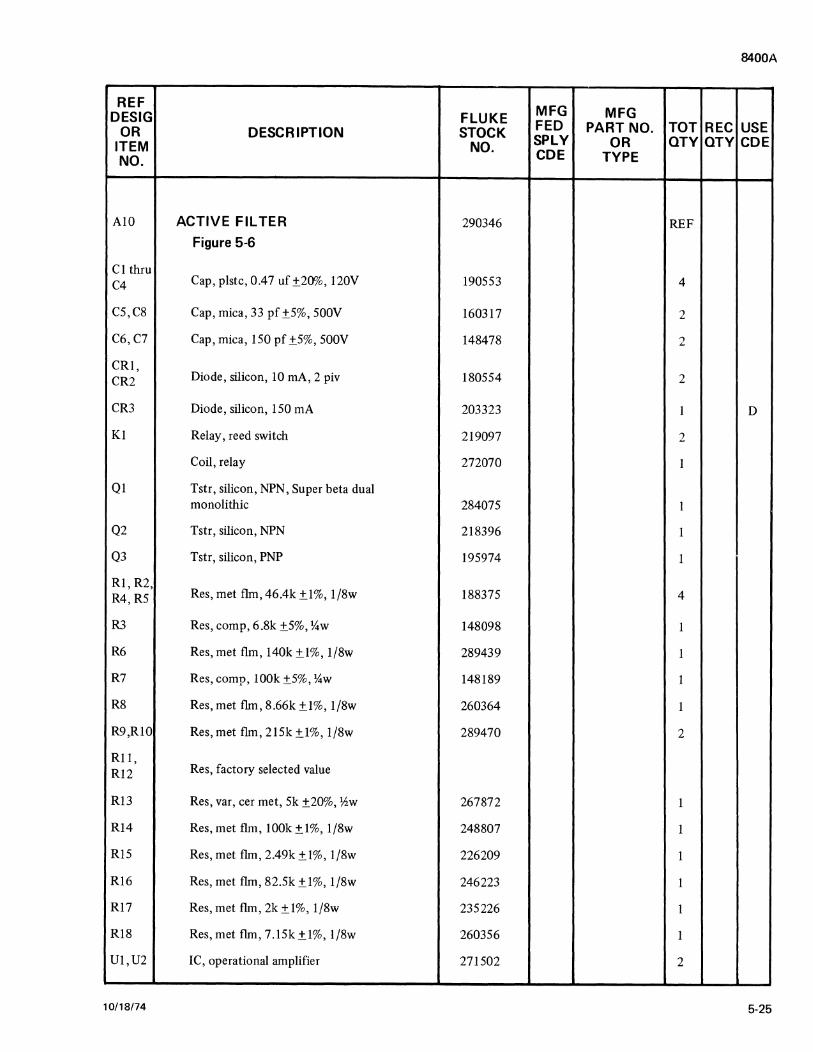
8400A
REF MFG MFG DESIG FLUKE
OR DESCRIPTION STOCK FED PART NO. TOT REC USE ITEM NO. SPLY OR QTY QTY COE NO. COE TYPE
AlO ACTIVE FILTER 290346 REF
Figure 5-6
Cl thru C4 Cap, plstc, 0.47 uf ±20%, I 20Y 190SS3 4
CS,C8 Cap, mica, 33 pf ±S%, SOOY 160317 2
C6,C7 Cap, mica, ISO pf ±S%, SOOY 148478 2
CRI, Diode, silicon, 10 mA, 2 piv 180SS4 CR2 2
CR3 Diode, silicon, 1 SO mA 203323 I D
Kl Relay, reed switch 219097 2
Coil, relay 272070 I
QI Tstr, silicon, NPN, Super beta dual monolithic 28407S I
Q2 Tstr, silicon, NPN 218396 I
Q3 Tstr, silicon, PNP 19S974 1
Rl,R2, Res, met flm, 46.4k ±1%, 1/8w 18837S 4 R4,RS
R3 Res, comp, 6.8k ±S%, %w 148098 1
R6 Res, met flm, 140k ±1%, 1/8w 289439 1
R7 Res, comp, lOOk ±S%, %w 148189 I
R8 Res, met flm, 8.66k ±1%, l/8w 260364 1
R9,R10 Res, met flm, 21Sk ±1%, 1/8w 289470 2
Rl 1, Res, factory selected value RI2
R13 Res, var, cermet, Sk ±20%, *w 267872 I
RI4 Res, met flm, 100k±1%, 1/8w 248807 1
RIS Res, met flm, 2.49k ±1%, 1/8w 226209 1
R16 Res, met flm, 82.Sk ±1%, 1/8w 246223 1
R17 Res, met flm, 2k ±1%, 1/8w 23S226 1
R18 Res, met flm, 7.1Sk±l%, 1/8w 2603S6 I
Ul,U2 IC, operational amplifier 271S02 2
10/18/74 5·25

8400A
Figure 5-6. ACTIVE FILTER PCB ASSEMBLY
5-26 10/18/74

8400A
REF MFG MFG DESIG FLUKE OR DESCRIPTION STOCK FED PART NO. TOT REC USE
ITEM NO. SPLY OR QTY QTY COE NO. COE TYPE
All BUFFER 288191 REF
Figure 5-7
Cl,C3 Cap, mica, 100 pf ±S%, SOOY 148494 2
C2,C4 Cap, mica, 33 pf ±S%, SOOY 160317 2
cs Cap, mica, 270 pf ±S%, SOOY 1484S2 1
C6,C7 Cap, cer, O.OS uf ±20%, lOOY 149161 2
C8 Cap, piste, 0.1 uf ±S%, lOOY 167460 1
C9,C10 Not Used
Cll Cap, mica, 2200 pf ±S%, SOOY 148346 1
CRl Diode, silicon, 10 mA, 2 piv 180SS4 1
CR2 Not Used
CR3 Diode, zener, 6.8Y 166199 1
CR4 thru Diode, silicon, 200 mA, 2S piv 190272 s CR8
CR9 thru Diode, germanium, 80 mA, 100 piv 149187 9 CR17
CR18 thru Diode, silicon, ISO mA 203323 7 CR24
Kl,K7 Relay, 4 PDT, SY coil • 272716 2
K2 Relay, reed switch 284091 1
Coil, relay 272070 1
K3 Relay, reed switch 284091 REF
Coil, relay 269019 4
K4,KS, Relay, reed switch K6 2898SO 3
Coil, relay 269019 REF
Ql,Q8 Tstr, silicon, PNP 19S974 2
Q2 Tstr, germanium, PNP 148643 1
Q3 Tstr, silicon, NPN 168716 1
10/18/74 5-27

8400A
REF MFG MFG DESIG FLUKE OR DESCRIPTION STOCK FED PART NO. TOT REC USE
ITEM NO. SPLY OR QTY QTY COE NO. COE TYPE
Q4 Tstr, silicon, NPN, dual, monolithic 295717 1
Q5 Tstr, silicon, NPN, Super beta dual CT> monolithic 284075 1
Q6,Q7 Tstr, silicon, PNP, selected 280198 2
Q9,Ql0 Not Used
Qll Tstr, selected 321638 1
Rl Res, comp, IM ±5%, %w 182204 1
R2 Res, comp, 47k ±5%, %w 150219 1
R4 Not Used
R3 Res, comp, 910k ±5%, 2w 110171 1
R5,R6 Ro<, WW, 4.45M } Matched Input R7 Res, ww, 899.55k Divider Set 284505 1 RIO Res, ww, 99.95k
R8 Res, var, cermet, lk ±20%, %w 267856 1
R9 Res, var, cermet, 100 ±20%, %w 267823 1
Rll Res, met flrn, lOk ±1%, 1/8w 168260 1
R12 Res, met flrn, 13.7k±1%, 1/8w 236752 1
R13 Res, met flrn, 34k ±1%, 1/8w 261602 1
R14 Res, met flrn, 2.6lk±1%, 1/8w 289983 1
R15 Res, met flrn, 232 ±5%, 1/8w 289975 1
R16 Res, met flrn, 84.5k ±1%, 1/8w 229492 1
R17 Res, var, cermet, 100k±20%, %w 268581 1
R18, Res, comp, lOOM ±10%, %w 190520 R19 2
R20, Res, comp, lOk ±5%, ¥.iw 148106 R33 2
R21 Res, comp, 270k ±5%, %w 220061 1
R22, R23,
Res, met flrn, factory selected value R25, R26
(may not be installed)
5-28 10/18/74

8400A
REF MFG MFG DESIG FLUKE
OR DESCRIPTION STOCK FED PART NO. TOT REC USE ITEM NO. SPLY OR QTY QTY COE NO. COE TYPE
R24, Res, met flm, 2M, Matched Set 290320 R27 1
R28 Res, var, cermet, lk ±10%, lw 285155 1 R
Res, var, cer met, lOk ± 10%, 1 w 285171 1 s R29 Res, met flm, 3.83M ±1%, 1hw 289660 1
R30, Res, comp, 22k ±5%, %w 148130 R31 2
R32 Res, comp, 470 ±5%, %w 147983 1
R34 Res, comp, 3.3k ±5%, %w 148056 1
R35 R", WW, 90k} R37 Res, ww, 9k Matched Output Divider Set 289686 1 R39 Res, ww lk
R36 Res, var, cermet, 200 ±20%, 1hw 284711 1
R38 Res, var, cermet, 20 ±20%, 1hw 261180 1
R40 Res, comp, 1±5%,1hw 218693 1
R41 Res, met flm, 499k ±1%, l/8w 268813 1
R42 Res, comp, lk ±5%, %w 148023 1
R43, Res, comp, 330 ±5%, %w R44 147967 2
Ul IC, operational amplifier [t:> 284760 1
U2 IC, operational amplifier 271502 1
U3 IC, voltage follower 288365 1
U4 IC, DTL, Quad 2-Input Nand Power Gate 288597 1
Socket, IC, U4 276527 1
Cover (not shown) 298893 1
[]::::>. Replacement of this part requires
factory recalibration. Return Al 1
buffer PCB only
10/18/74 5-29

8400A
Figure 5-7. BUFFER AMPLIFIER PCB ASSEMBLY
5-30 10/18/74

8400A
REF MFG MFG DESIG FLUKE OR DESCRIPTION STOCK FED PART NO. TOT REC USE
ITEM NO. SPLY OR QTY QTY COE
NO. COE TYPE
Al4 DISPLAY 288167 REF
Figure 5-8
CI Cap, cer, O.OS uf ±20%, SOV 149161 I
C2 Cap, cer, 300 pf±l0%, SOOV IOS734 1 p
C2, Cap, cer, 1200 pf ±10%, SOOV ClOO 106732 2 Q
C3 Cap, elect, 20 uf +S0/-10%, 16V 2413S6 I
C4 Cap, cer, 0.02S uf ±20%, SOV 16843S I
cs Cap, cer, O.OOS uf ±20%, SOV l 7S232 I p
cs Cap, cer, 2200 pf ±10%, SOOV 26842S I Q
C6 Cap, cer, 0.01 uf ±20%, lOOV (on bottom side 1491S3 I p
of PCB)
C6, Cap, cer, O.Oluf±20%, lOOV C103 149IS3 2 Q
ClOl Cap, cer, SOO pf ±10%, SOOV 10S692 1 Q
C102 Cap, cer, 0.02S uf ±20%, SOV 17S232 I Q
CRI, CR2, CR7, CRIO, CR12, CRI6, CR18, Diode, germanium, 80 mA, 100 piv 149187 lS p
CR19, CR2S thru CR30, CR32
CRI, CR2, CR7, CRIO, CRI2,
Diode, germanium, 80 mA, 100 piv CR16, 149187 16 Q
CR18, CRI9, CR2S thru CR30,
10/18/74 5-31
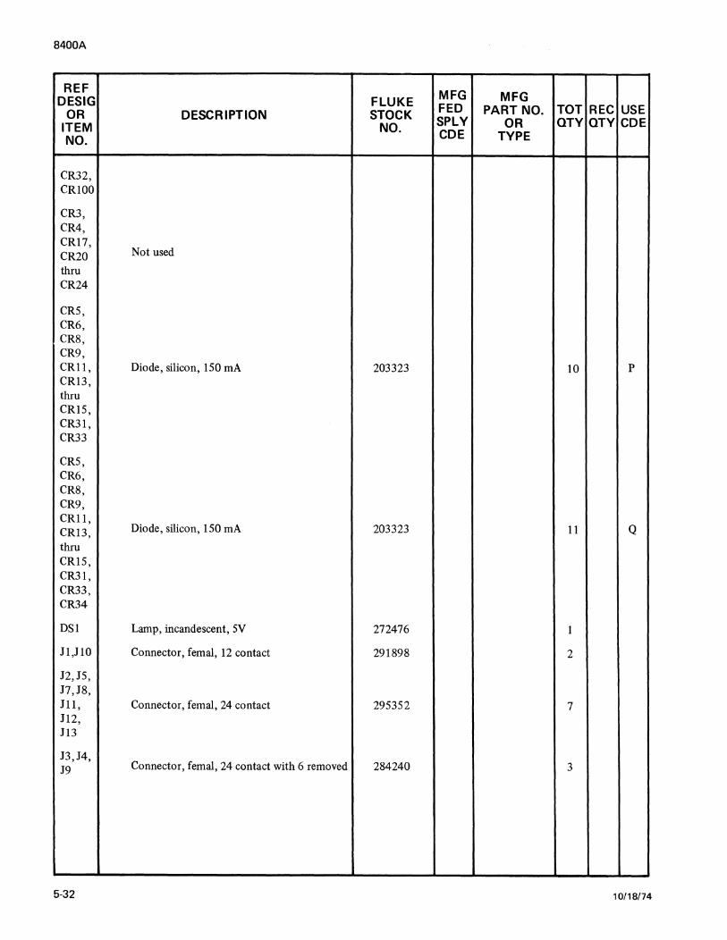
8400A
REF MFG DESIG FLUKE MFG OR DESCRIPTION STOCK FED PART NO. TOT REC USE
ITEM NO. SPLY OR QTY QTY COE NO. COE TYPE
CR32, CRlOO
CR3, CR4, CRI7,
Not used CR20 thru CR24
CRS, CR6, CR8, CR9, CRll, Diode, silicon, ISO mA 203323 10 p CR13, thru CRIS, CR3I, CR33
CRS, CR6, CR8, CR9, CRII,
Diode, silicon, I SO mA CR13, 203323 11 Q thru CRIS, CR3I, CR33, CR34
DSI Lamp, incandescent, SY 272476 I
Jl,JIO Connector, femal, I2 contact 29I898 2
J2,JS, J7,J8, Jll, Connector, femal, 24 contact 29S3S2 7 112, J13
J3,J4, Connector, femal, 24 contact with 6 removed J9 284240 3
5-32 10/18/74

8400A
REF MFG DESIG FLUKE MFG OR DESCRIPTION STOCK FED PART NO. TOT REC USE
ITEM NO. SPLY OR QTY QTY COE NO. COE TYPE
JI4 Connector, female, 18 contact 291906 I
QI,Q2 Not used
Q2,Q5 Tstr, silicon, PNP 195974 2
Q3,Q6 Q7,QI~
Q20, Tstr, silicon, NPN Q34,
218396 8
Q35, Q36
Q4,Q8 Tstr, silicon, unijunction 268110 2
Q9 thru Tstr, silicon, NPN 245480 IO Ql8
Q22 thru Tstr, silicon, NPN 218511 5 Q26
Q27 thru Tstr, silicon, PNP 266619 5 Q31
Q33, Q33 Tstr, FET, N-channel 288324 2
Q37 Tstr, silicon, NPN 168708 I
RIOR3 R6 Not used
R2,R4 Res, comp, 82k ±5%, %w 188458 2
RS Res, comp, 6.8k ±5%, %w 148098 1
R6, RI I,
Res, co np, 3.9k ±5%, %w 148064 R20, 4
R25
R7, Res, comp, 470 ±5%, %w R58 147983 2
R8, Rl8 Res, comp, 2.7k ±5%, %w 170720 2
R9, Res, comp, 12k ±5%, %w (R63 on bottom R63 side of PCB) 159731 2 p
10/18/74 5-33
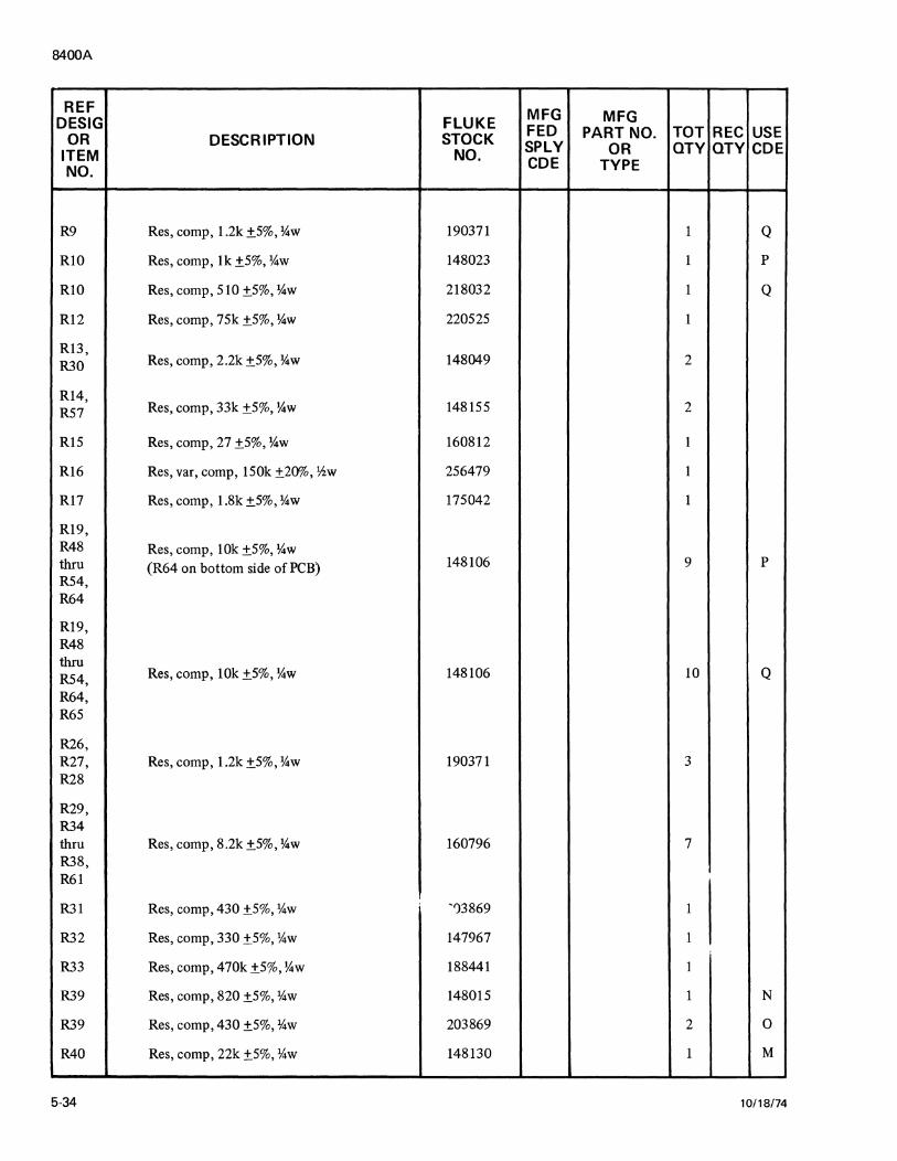
8400A
REF MFG MFG DESIG FLUKE OR DESCRIPTION STOCK FED PART NO. TOT REC USE
ITEM NO. SPLY OR QTY QTY COE NO. COE TYPE
R9 Res, comp, 1.2k ±5%, %w 190371 1 Q
RIO Res, comp, lk ±5%, %w 148023 1 p
RIO Res, comp, 5 IO ±5%, %w 218032 1 Q
R12 Res, comp, 75k ±5%, %w 220525 1
Rl3, Res, comp, 2.2k ±5%, %w 148049 R30 2
R14, Res, comp, 33k ±5%, %w 148155 R57 2
R15 Res, comp, 27 ±5%, %w 160812 1
R16 Res, var, comp, 150k ±20%, ~w 256479 1
R17 Res, comp, 1.8k±5%, %w 175042 1
R19, R48 Res, comp, IOk ±5%, %w thru (R64 on bottom side of PCB) 148I06 9 p
R54, R64
Rl9, R48 thru R54, Res, comp, IOk ±5%, %w 148I06 IO Q
R64, R65
R26, R27, Res, comp, 1.2k ±5%, %w 190371 3 R28
R29, R34 thru Res, comp, 8.2k ±5%, %w 160796 7 R38, R61
R31 Res, comp, 430 ±5%, %w '')3869 1
R32 Res, comp, 330 ±5%, %w 147967 1
R33 Res, comp, 470k ±5%, %w 188441 1
R39 Res, comp, 820 ±5%, %w 148015 1 N
R39 Res, comp, 430 ±5%, %w 203869 2 0
R40 Res, comp, 22k ±5%, %w 148130 1 M
5-34 10/18/74

8400A
REF MFG MFG OESIG FLUKE OR DESCRIPTION STOCK FED PART NO. TOT REC USE
ITEM NO. SPLY OR QTY QTY COE NO. COE TYPE
R40 Res, comp, 4.7k ±5%, ~w 148072 I K
R41 Res, comp, 2.7k ±5%, ~w 170720 1 N
R41 Res, comp, 5.lk ±5%, ~w 193342 I 0
R43 thru R46,
Res, comp, 39 ±5%, ~w R55, 193391 7
R56, R62
R47 Res, comp, 3.3k ±5%, ~w 148056 1
Switch Assembly 298232 1
Switch section, SI thru S7, RANGE 288688 1
Switch section, S8 thru S14, FUNCTION 288670 1
Flex circuit 207504 1
U1 IC, TTL, Hex Inverter Buffer Driver 288605 I
U2,U3 IC, TTL, dual J-K flip flop 268441 2
U4 IC, Decoder Driver, DM/SN7441AN, 267211 1 NS8840N
VI Tube, polarity indicator 272922 I
V2 thru Tube, neon readout 271494 6 V7
Display, function assembly (lamp, P/N 272476 may be purchased separately) 291542 I Socket, IC, 14 contact
Socket, IC, 16 contact 291534 3
10/18/74 5-35

8400A
-
Figure 5-8. DISPLAY PCB ASSEMBLY
5-36 10/18/74
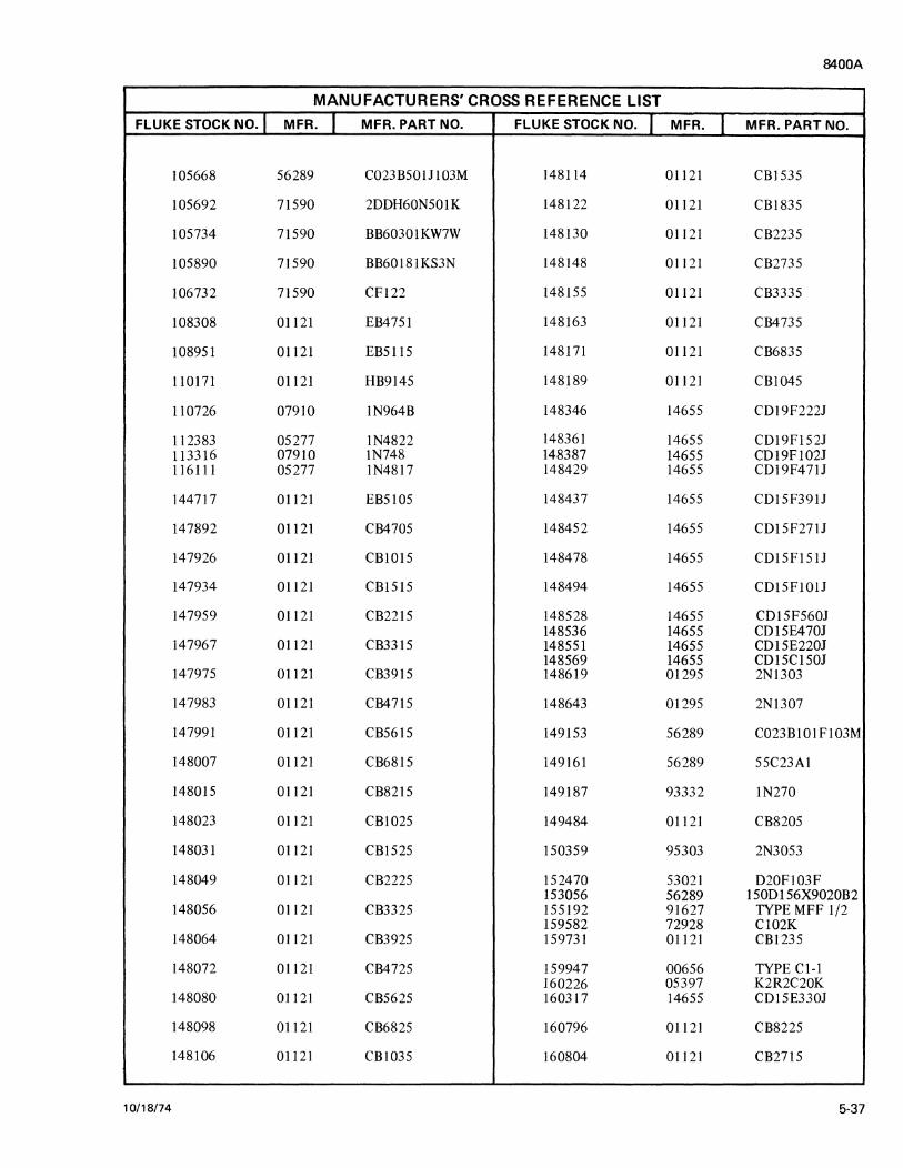
8400A
MANUFACTURERS' CROSS REFERENCE LIST
FLUKE STOCK NO.} MFR. I MFR. PART NO. FLUKE STOCK NO. I MFR. I MFR. PART NO.
105668 56289 C023850IJ103M 148114 01121 CBI 535
105692 71590 2DDH60N501K 148122 01121 CB1835
105734 71590 BB60301KW7W 148130 01121 CB2235
105890 71590 BB60181KS3N 148148 01121 CB2735
106732 71590 CF122 148155 01121 CB3335
108308 01121 EB4751 148163 01121 CB4735
108951 01121 EB5115 148171 01121 CB6835
110171 01121 HB9145 148189 01121 CB1045
110726 07910 1N964B 148346 14655 CDI9F222J
112383 05277 1N4822 148361 14655 CD19Fl52J 113316 07910 1N748 148387 14655 CD19F102J 116111 05277 1N4817 148429 14655 CD19F471J
144717 01121 EB5105 148437 14655 CDI5F391J
147892 01121 CB4705 148452 14655 CD15F271J
147926 01121 CB1015 148478 14655 CDI5Fl51J
147934 01121 CB1515 148494 14655 CD15Fl01J
147959 01121 CB2215 148528 14655 CDI5F560J 148536 14655 CD15E470J
147967 01121 CB3315 148551 14655 CD15E220J 148569 14655 CD15C150J
147975 01121 CB3915 148619 01295 2Nl303
147983 01121 CB4715 148643 01295 2Nl307
147991 01121 CB5615 149153 56289 C023B101F103M
148007 01121 CB6815 149161 56289 55C23Al
148015 01121 CB8215 149187 93332 1N270
148023 01121 CB1025 149484 01121 CB8205
148031 01121 CB1525 150359 95303 2N3053
148049 01121 CB2225 152470 53021 D20Fl03F 153056 56289 1500156X9020B2
148056 01121 CB3325 155192 91627 TYPE MFF 1/2 159582 72928 Cl02K
148064 01121 CB3925 159731 01121 CB1235
148072 01121 CB4725 159947 00656 TYPE Cl-1 160226 05397 K2R2C20K
148080 01121 CB5625 160317 14655 CD15E330J
148098 01121 CB6825 160796 01121 CB8225
148106 01121 CB1035 160804 01121 CB2715
10/18/74 5-37
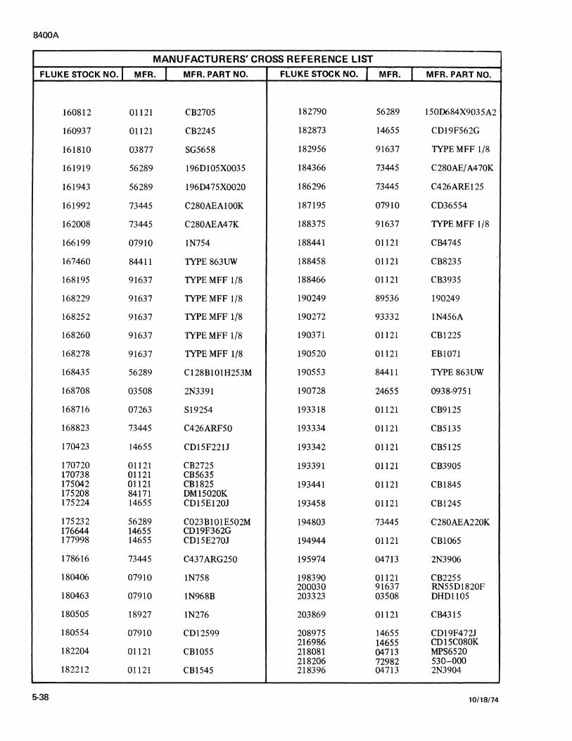
8400A
MANUFACTURERS' CROSS REFERENCE LIST
FLUKE STOCK NOJ MFR. l MFR. PART NO. FLUKE STOCK NO. l MFR. I MFR. PART NO.
160812 01121 CB2705 182790 56289 l 50D684X903 5A2
160937 01121 CB2245 182873 14655 CD19F562G
161810 03877 SG5658 182956 91637 TYPEMFF 1/8
161919 56289 196D105X0035 184366 73445 C280AE/ A4 70K
161943 56289 196D475X0020 186296 73445 C426ARE125
161992 73445 C280AEA1 OOK 187195 07910 CD36554
162008 73445 C280AEA47K 188375 91637 TYPE MFF 1/8
166199 07910 1N754 188441 01121 CB4745
167460 84411 TYPE863UW 188458 01121 CB8235
168195 91637 TYPEMFF 1/8 188466 01121 CB3935
168229 91637 TYPEMFF 1/8 190249 89536 190249
168252 91637 TYPEMFF 1/8 190272 93332 1N456A
168260 91637 TYPEMFF 1/8 190371 01121 CB1225
168278 91637 TYPEMFF 1/8 190520 01121 EB1071
168435 56289 Cl 28Bl01H253M 190553 84411 TYPE 863UW
168708 03508 2N3391 190728 24655 0938-9751
168716 07263 Sl9254 193318 01121 CB9125
168823 73445 C426ARF50 193334 01121 CB5135
170423 14655 CD15F221J 193342 01121 CB5125
170720 01121 CB2725 193391 01121 CB3905 170738 01121 CB5635 175042 01121 CB1825 193441 01121 CB1845 175208 84171 DM15020K 175224 14655 CD15E120J 193458 01121 CB1245
175232 56289 C023B101E502M 194803 73445 C280AEA220K 176644 14655 CD19F362G 177998 14655 CD15E270J 194944 01121 CB1065
178616 73445 C437ARG250 195974 04713 2N3906
180406 07910 1N758 198390 01121 CB2255 200030 91637 RN55D1820F
180463 07910 1N968B 203323 03508 DHD1105
180505 18927 1N276 203869 01121 CB4315
180554 07910 CD12599 208975 14655 CD19F472J 216986 14655 CD15C080K
182204 01121 CB1055 218081 04713 MPS6520 218206 72982 530-000
182212 01121 CB1545 218396 04713 2N3904
5-38 10/18/74

8400A
MANUFACTURERS' CROSS REFERENCE LIST
FLUKE STOCK NO.} MFR. I MFR. PART NO. FLUKE STOCK NO. l MFR. l MFR. PART NO.
237297 91637 TYPEMFF 1/8 218511 95303 60994 240937 89536 240937
218693 01121 EB1065 241091 91637 TYPE MFF 1/8
219097 15898 765972 241356 73445 C426ARE20
220061 01121 CB2735 241471 91637 TYPE MFF 1/8
220525 01121 CB7535 241497 91637 TYPE MFF 1/8
220541 01121 CB8245 245480 07263 S24496
221580 01121 CB1135 246066 04713 EL131
221606 01121 CB1635 246223 91637 TYPE MFF 1/8 221614 01121 CB2035 246611 07910 1N961B 221903 01121 CB6215 248807 91637 TYPE MFF 1/8
221911 01121 CB6225 248906 95303 CA3046 221937 01121 CB7545 221952 01121 CB3055 249052 07910 1N963B
221960 01121 CB6255 249284 '/1536 249284
225599 07263 S22650 256479 71450 TYPE45
226134 14655 CD15F151F500 257501 17856 DN423
226209 91637 TYPE MFF 1/8 260356 91637 TYPE MFF 1/8 226274 82389 46256LFE 226316 00656 TYPE MFF Cl-I 260364 91637 TYPEMFF 1/8
229146 91637 TYPEMFF 1/8 260547 91637 TYPEMFF 1/8 229476 91637 TYPEMFF 1/8 229484 91637 TYPEMFF 1/8 260554 07910 CD55105
229492 91637 TYPE MFF 1/8 260562 84411 863UW47391 260695 07910 1N754A
229898 04713 MPS6522 261180 71450 190PC200B 229930 91293 JMC2951 234484 73445 C280AEA22K 261370 22767 Sl330 234492 73445 C280AEA33K 234682 01121 CB3045 261388 04713 SPF179 234708 91637 TYPE MFF 1/8 234971 91637 TYPEMFF 1/8 261602 91637 TYPEMFF 1/8
235266 91637 TYPEMFF 1/8 261651 91637 TYPEMFF 1/8
235234 91637 TYPE MFF 1/8 261842 01121 CB6205
235309 91637 TYPEMFF 1/8 261883 91637 TYPE MFF 1/8
235333 91637 TYPEMFF 1/8 266312 04713 MC862P
236752 91637 TYPEMFF 1/8 266619 07263 2N4888 236802 91637 TYPE MFF 1/8 236901 73445 C437ARF160 267120 73445 C280AE/ A27K
236935 73445 C426ARD200 267153 04713 MC839P
237206 91637 TYPEMFF 1/8 267211 89536 267211
10/18/74 5-39
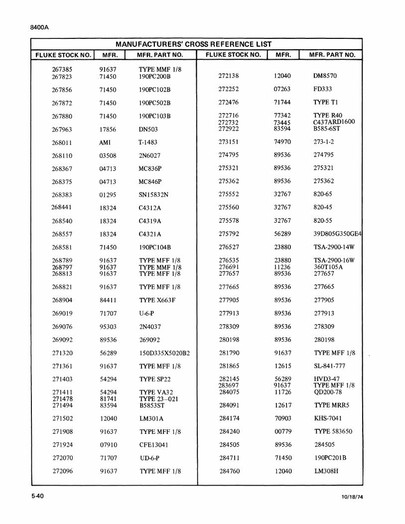
8400A
MANUFACTURERS' CROSS REFERENCE LIST
FLUKE STOCK NO.] MFR.] MFR. PART NO. FLUKE STOCK NO. l MFR. l MFR. PART NO.
267385 91637 TYPE MMF 1/8 267823 71450 190PC200B 272138 12040 DM8570
267856 71450 190PC102B 272252 07263 FD333
267872 71450 190PC502B 272476 71744 TYPE Tl
267880 71450 190PC103B 272716 77342 TYPE R40 272732 73445 C437ARD1600
267963 17856 DN503 272922 83594 B585-6ST
268011 AMI T-1483 273151 74970 273-1-2
268110 03508 2N6027 274795 89536 274795
268367 04713 MC836P 275321 89536 275321
268375 04713 MC846P 275362 89536 275362
268383 01295 SN15832N 275552 32767 820-65
268441 18324 C4312A 275560 32767 820-45
268540 18324 C4319A 275578 32767 820-55
268557 18324 C4321A 275792 56289 39D805G350GE4
268581 71450 190PC104B 276527 23880 TSA-2900-14W
268789 91637 TYPE MFF 1/8 276535 23880 TSA-2900-16W 268797 91637 TYPE MMF 1/8 276691 11236 360T105A 268813 91637 TYPE MFF 1/8 277657 89536 277657
268821 91637 TYPE MFF 1/8 277665 89536 277665
268904 84411 TYPE X663F 277905 89536 277905
269019 71707 U-6-P 277913 89536 277913
269076 95303 2N4037 278309 89536 278309
269092 89536 269092 280198 89536 280198
271320 56289 150D335X5020B2 281790 91637 TYPE MFF 1/8
271361 91637 TYPE MFF 1/8 281865 12615 SL-841-777
271403 54294 TYPE SP22 282145 56289 HVD3-47 283697 91637 TYPE MFF 1/8
271411 54294 TYPE VA32 284075 11726 QD200-78 271478 81741 TYPE 23-021 271494 83594 B5853ST 284091 12617 TYPEMRR5
271502 12040 LM301A 284174 70903 KHS-7041
271908 91637 TYPE MFF 1/8 284240 00779 TYPE 583650
271924 07910 CFE13041 284505 89536 284505
272070 71707 UD-6-P 284711 71450 190PC201B
272096 91637 TYPE MFF 1/8 284760 12040 LM308H
5-40 10/18/74

8400A
MANUFACTURERS' CROSS REFERENCE LIST
FLUKE STOCK NO.} MFR. I MFR. PART NO. FLUKE STOCK NO. l MFR. l MFR. PART NO.
284885 84411 863UW33351 288563 91637 TYPE MFF 1/8
284968 75042 TYPEMEH 288597 04713 MC858P
284976 91637 TYPE MFF 1/4 288605 01295 SN7416P
285031 75915 279.015 288639 91637 TYPEMFF 1/8 285106 07910 CRE3021 285114 71450 360S-200B 288647 89536 288647
285122 71450 360S-500A 288654 89536 288654
285130 71450 360S-101A 288670 89536 288670
285148 71450 360S201A 288688 89536 288688
285155 71450 360S-102A 288761 49956 RS2048
285163 71450 360S-202A 288803 01295 SN158097N 288811 01537 MC856P
285171 71450 360S-103A 288837 01295 SN74100N
285189 91637 TYPEMFF 1/8 288845 01295 SN7402N
285213 71450 190PC253B 288852 04713 MC8312P
285239 89536 285239 288928 12040 LM308AH
285361 89536 285361 289066 91637 TYPE MFF 1/8
288043 89536 288043 289439 91637 TYPE MFF 1/8
288159 89536 288159 289470 91637 TYPEMFF 1/8
288167 89536 288167 289637 72982 538-006D-9-35
288175 89536 288175 289660 00327 TYPEM12
288183 89536 288183 289686 89536 289686
288191 89536 288191 289850 12617 TYPEMRR2
288209 89536 288209 289975 91637 TYPEMFF 1/8
288217 89536 288217 289983 91637 TYPE MFF 1/8
288225 89536 288225 290130 89536 290130
288233 89536 288233 290148 89536 290148
288308 71450 360S-104A 290155 89536 290155
288324 15818 U2412 290163 89536 290163
288365 12040 LM310H 290247 89536 290247
288381 95303 40372 290262 89536 290262 288480 91637 TYPE MFF 1/8 288498 91637 TYPEMFF 1/8 290270 89536 290270
288555 91637 TYPEMFF 1/8 290296 89536 290296
10/18/74 5-41

8400A
MANUFACTURERS' CROSS REFERENCE LIST
FLUKE STOCK NO. ( MFR. ( MFR. PART NO. FLUKE STOCK NO. I MFR. l MFR. PART NO.
290304 89536 290304 298893 89536 298893
290312 89536 290312 298992 89536 298992
290320 89536 290320 299610 89536 299610
290346 89536 290346 301382 89536 301382
290650 89536 290650 301390 89536 301390
291120 71450 360S501A 303412 89536 303412 291294 91637 TYPEMFF 1/8 291526 89536 291526 303461 89536 303461
291534 00779 583529 306118 01295 GA3938A
291542 00779 583527 306126 01295 GA3937A
291690 89536 291690 307298 89536 307298
291898 00779 583650-2 307504 89536 307504
291906 00779 583650-3 309633 77342 TYPER40
292193 89536 292193 309849 72982 8131-050-651-224M
292201 89536 292201 311746 89536 311746
292888 89536 292888
292896 89536 292896 321398 89536 321398
292904 89536 292904 329912 12040 LM318H
292946 71785 133-59-02-011 334722 71450 360Sl05A 292953 01537 MC7400P 292979 01295 SN7404N 339309 89536 339309
295121 89536 295121 340133 91637 TYPEMFF%
295196 56289 39D718G010JP4 340158 91637 TYPEMFF%
295337 28213 SF3402 340166 91637 TYPEMFF 1/8
295352 00779 583650-9 340208 91637 TYPEMFF 1/8
295535 89536 295535 340216 91637 TYPE MFF 1/8
295717 11726 QD101-78E 340224 91637 TYPE MFF 1/8 296582 75915 281005 340232 91637 TYPEMFF 1/8 297713 89536 297713 340240 91637 TYPEMFF 1/8 297762 89536 297762 340257 91637 TYPEMFF 1/8 297903 89536 297903
340265 03888 TYPEPME75 298232 89536 298232
340273 95275 VY10CA2R2CA 298554 89536 298554
5-42 10/tS/74

8400A
MANUFACTURERS' CROSS REFERENCE LIST
FLUKE STOCK NO.] MFR.] MFR. PART NO. FLUKE STOCK NO. l MFR. l MFR. PART NO.
340315 91637 TYPE MFF 1/8
340323 91637 TYPEMFF ~
340745 95275 VY IOCA2R 7CA
342873 73445 C280AEA10K
342881 73445 C280AEA6K8
344283 95275 VYIOCA270JA
347963 80294 3329H-J81-3RO
10/18/74 5-43/5-44


8400A
Section 6
Option & Accessory Information
6-1. INTRODUCTION
6-2. This section contains information describing the options and accessories usable with this instrument.
6-3. OPTIONS
6-4. Each of the options usable with this instrument are described under headings that list the option name and number. The descriptions give detailed field installation, opera-
ting, and maintenance data for each option as well as a complete list of replaceable parts.
6-5. ACCESSORIES
6-6. Accessories usable with this instrument are describ-ed under headings that list the accessory name and number.
6-7. A listing of included options and accessories is given in the contents at the front of this manual.
6-1


6-1. INTRODUCTION
6-2. The Al 3 AC Converter (Drawing No. 8400A-1007) when used in conjunction with the 8400A DVM provides an ac voltage measurement capability through four ranges of 1, 10, 100, and 1000. The converter rectifies ac input voltage to de and applies the de to the A9 A-to-D Converter for measurement in exactly the same manner as described in the Theory of Operation for measurement of de voltage.
6-3. SPECIFICATIONS
6-4. AC Converter specifications are given in Section 1, Introduction and Specifications.
6-5. INSTALLATION
6-6. Use the following procedure to install the AC Con-verter Option in the 8400A DVM.
a. With the DVM disconnected from the power source, remove the top dust and chassis guard covers. On the Al4 Display Motherboard in the instrument, determine that connector 113 is clear of obstructions and that alignment key is inserted between pin pairs 113-23, -24and113-21, -22. See Drawing No. 8400-1002, Sheet 1 of 2. Locate terminal block No. 1 terminals P2TF and P2TR and connect the red and black wires from the AC Converter board to these terminals, respectively.
b. Check that shield on AC Converter is securely attached to board and align board vertically with plastic guide slots on inner vertical faces of guard chassis. Align rubber grommet with slot in front
c.
AC
8400A OPTION-01
Option -01
Converter
guard chassis and insert. Slide converter board downward to fully engage board card edge connector with 113 connector on Motherboard.
Attach guard and instrument dust cover, connect ac power, and perform receiving inspection test of converter as described in paragraph 6-22, Performance Test.
6-7. OPERATING INSTRUCTIONS
6-8. Operation of the DVM with the Al3 AC Converter Option 8400-01 installed is covered in Section 2, Operating Instructions.
6-9. THEORY OF OPERATION
6-10. General
6-11. The Al 3 AC Converter consists of two basic parts as shown in Figure 6-1 : an operational rectifier and a de difference amplifier integrator. The operational rectifier consists of an inverting, trans-conductance amplifier and load resistor with negative feedback arranged to provide a loop gain of about 5 X 10³ at midband. The feedback is changed with reed switches for range purposes. The input resistor is 1.11 megohms and this value provides 1.11 megohm input impedance at the DVM input jacks. A symmetrical half-wave rectifier placed between the amplifier and load resistor develops equal positive and negative de voltages proportional to the amplifier output current. At full scale, this current is near two milliamps. The two output waveforms are shown in Figure 6-2.
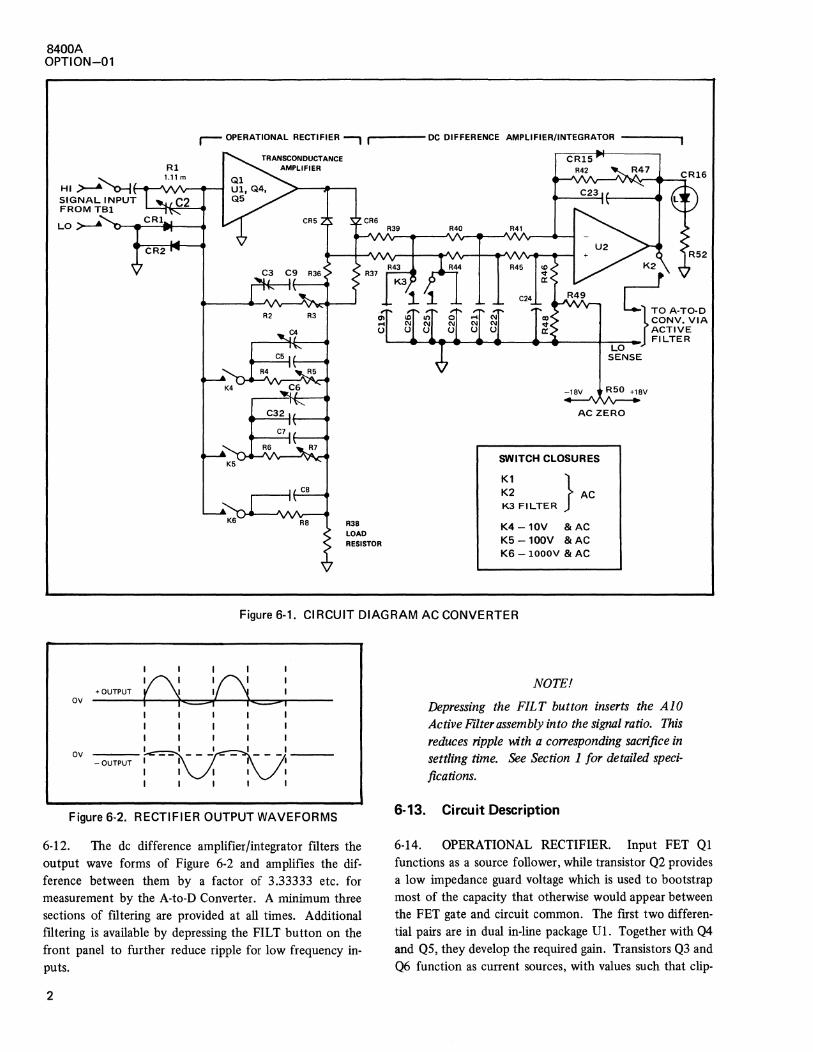
8400A OPTION-01
r- OPERATIONAL RECTIFIER l ---- OC DIFFERENCE AMPLIFIER/INTEGRATOR ----
SIGNAL INPUT FROM TBl
Rl 1.11 m
LO >---6 'n--.-:--::a~---
R38 LOAD RESISTOR
CR15
LO SENSE
-18V R50 +18V
AC ZERO
SWITCH CLOSURES
K1 } K2 AC K3 FILTER
K4-10V & AC K5-100V &AC K6 - lOOOV & AC
Figure 6-1. CIRCUIT DIAGRAM AC CONVERTER
I I I I I
+OUTPUT ("l~q : ov ____, <::::='* I
I I I I I I I I I I I I
ov I I I I I ---0-UT-PU-T-:v.v,---
I I I I I
Figure 6-2. RECTIFIER OUTPUT WAVEFORMS
6-12. The de difference amplifier/integrator filters the output wave forms of Figure 6-2 and amplifies the difference between them by a factor of 3.33333 etc. for measurement by the A-to-D Converter. A minimum three sections of filtering are provided at all times. Additional filtering is available by depressing the FILT button on the front panel to further reduce ripple for low frequency inputs.
2
NOTE!
Depressing the FILT button inserts the AlO Active Filter assembly into the signal ratio. This
reduces ripple with a co"esponding sacrifice in settling time. See Section 1 for detailed speci
fications.
6-13. Circuit Description
6-14. OPERATIONAL RECTIFIER. Input FET Ql functions as a source follower, while transistor Q2 provides a low impedance guard voltage which is used to bootstrap most of the capacity that otherwise would appear between the FET gate and circuit common. The first two differential pairs are in dual in-line package U1. Together with Q4 and QS, they develop the required gain. Transistors Q3 and Q6 function as current sources, with values such that clip-

ping due to overload is symmetrical. Changes in capacitor charges are small and amplifier recovery time is minimized. Transistor Q7 compensates for capacitance losses in the diodes.
6-15. DC-DIFFERENCE AMPLIFIER/INTEGRATOR. The filter network, which provides the input to the amplifier/integrator, consists of resistors R39, R40, R41, R43, R44, R45 and capacitors Cl9, C20, C21, C22, C25 and C26. Capacitors Cl9, C21, C23 and C26 form matched pairs with capacitors C20, C22, C24, and C25, respectively, to maintain good common-mode rejection. Gain for the de amplifier is provided by monolithic operational amplifier U2, thereby providing a total loop gain at de of about 5 X 10⁵ •
6-16. RANGE AND FUNCTION CONTROL. The converter input and output relays, Kl and K2, are operated from the V AC control line. The range relays, K4 through K6, are operated by driver circuitry consisting of NAND gates U4A, C, D and associated components. These range control gates accept the buffered outputs of the range counter on the Al4 Display board. U3B and U4B deliver the up and down range stop commands, for V AC function, to A2 Range Delay board. The NAND gates U3A and U3C deliver the set and reset commands to the range counter, on Al 4 Display board, for prevention of a disallowed range in the V AC function.
6-17. MAINTENANCE
6-18. Introduction
6-19. This section contains maintenance information specifically intended for the AC Converter. Factory service information and general instructions regarding instrument access and cleaning are located in Section 4 of the Manual.
6-20. Test Equipment
6-21. The following equipment is recommended for test-ing, troubleshooting, and calibrating the AC Converter. If the recommended equipment is not available, equivalent or better instruments may be substituted.
10/18/74
8400A OPTION-01
EQUIPMENT RECOMMENDED NOMENCLATURE EQUIPMENT
AC Voltage Source HP Model 745A AC Calibrator with companion 1000 volt amplifier.
Multimeter Fluke Model 8 lOOA Digital Multimeter
Oscilloscope Tektronix Model 54 7
Oscilloscope Tektronix Model IAl Plug-In
6-22. Performance Test
6-23. The performance test in this section compares the AC Converter performance to the accuracy specifications in Section 1 of the manual to determine if the converter is in calibration. Known ac voltages are applied to the DVM input terminals on each of the four ranges. The performance test should be conducted before any instrument maintenance or calibration is attempted. The test is also suited to receiving inspection of new converters. The performance test should be conducted under the following environmental conditions after 1 hour warm up: ambient temperature 23°C ±2°C, relative humidity less than 70%. An instrument that fails the performance test will require corrective maintenance or calibration. In case of difficulty, analysis of the test results with reference to the troubleshooting section, should help to locate the trouble.
NOTE!
Permissible tolerances for ac voltage measurements are derived from the 90-day instrument specifications contained in Section 1 of the manual.
6-24. AC VOLTAGE TEST. In the following procedure, 10 kHz voltages are applied to the instrument at 100% of full-scale on the 1, 10, and 100 volt ranges and at 0.1 % and 100% of full-scale on the 1000 volt range.
a. Set the DVM controls as follows:
VAC FUNCTION RANGE Manually selected, as required.
3

8400A OPTION-01
b. Apply each of the 10 kHz test signals shown in Figure 6-3 to the INPUT terminals of the DVM. The readout should be as indicated.
INPUT RANGE READOUT LIMITS
(VAC)
1 1 .99945 to 1.00055 10 10 9.9945 to 10.0055 100 100 99.945 to 100.055 1 1000 000.95 to 001.05 1000 1000 999.00 to 1001.00
Figure 6-3. AC VOLTAGE TEST REQUIREMENTS
6-25. Calibration
The AC Converter should be calibrated every 90 days, or whenever repairs have been made to circuitry. Calibration of the converter should be performed at an ambient room temperature of 23°C ±5°C. Relative humidity should be less than 70%. Consult paragraph 6-20 for recommended test equipment.
6-26. PRELIMINARY OPERATIONS
a. Remove the upper dust cover retaining screws, but leave the dust cover in place on the instrument.
b.
c.
Set the rear panel 115/230 volts slide switch to the 115 volt position and connect the line cord to an autotransformer set to 120 volts ac.
Turn on and allow the instrument to operate for one hour.
6-27. AC CONVERTER ALIGNMENT
a. Set the DVM controls as follows:
b.
4
FUNCTION V AC RANGE 1000 SAMPLE RA TE Fully clockwise
Connect the GUARD terminal to the LO input terminal using the shorting link provided.
c. Connect a shorting jumper between the INPUT terminals.
d. Adjust AC zero for 000.00 on the readout.
e. Rotate the .OOlV 50 kHz adjustment (AB C18) slowly in a CW direction. Note that one digit will be displayed longer than the others. When this "long duration digit" changes to a new number STOP; back the adjustment off so that the "long duration digit" just remains steady on the readout.
f. Readjust AC zero for 000.00 on the readout.
g.
h.
Remove the short between the INPUT terminals.
Perform the checks and adjustments contained in Figure 6-4.
6-28. Calibration of the AC Converter is now complete.
6-29. Troubleshooting
6-30. This section contains information selected to aid in troubleshooting the AC Converter. Before attempting to troubleshoot the unit, however, it should be verified that the trouble is actually in the converter and is not caused by faulty external equipment or improper control settings. For this reason, the performance test (paragraph 6-22) is suggested as a first step in troubleshooting. The performance test may also help to localize trouble to a particular section of the instrument. If the performance test fails to localize the trouble, the following information may be helpful.
6-31. POWER SUPPLY VOLTAGE CHECK
6-32. In this test, each of the supply voltages for the AC Converter is checked at the pin connectors. This test verifies only presence of voltages; a detailed check of the DVM power supply voltages is given in Section 4.
a. Connect the oscilloscope common to TP2 of the converter. Use the internal de oscilloscope trigger. Set the scope controls for de voltage measurement, and check the following voltages:
Connector Required Pin No. Voltage
21 -18 volts 19 +18 volts
6-33. COMMAND VOLTAGE CHECK
6-34. The presence of proper command voltages is check-ed in the following test:
10/18/74

a.
b.
Connect the oscilloscope common to the converter as indicated in the preceeding test.
Perform each of the connector pin voltage checks given in Figure 6-5. The voltages should be as indicated.
INPUT
6-35. RELAY CHECKS
8400A OPTION-01
The truth table (Figure 6-6) will help locate defective relays or associated drive circuits. Assuming there are no errors in the command voltage check, if the voltage across the coil does not appear as indicated on the truth
TOLERANCE STEP RANGE ADJUSTMENT (±DIGITS) FREQ VOLTS
1 500 Hz .001 1 Check Only 3 2 50 kHz .001 1 .001V 50 kHz (A13C18) Same reading as Step! 3 500 Hz 500.00 1000 500V 1 kHz (A 13R47) 3 4 30 kHz 500.00 1000 500V 30 kHz (A 13C2) 3 5 500 Hz 1.0000 1 1V 500 Hz (A13R3) 5 6 50 kHz 1.0000 1 1V 50 kHz (A13C3) 5 7 100 kHz 1.0000 1 Check Only 200 8 20 kHz 1.0000 1 Check Only 20 9 50 Hz 1.0000 1 Check Only 30
10 500 Hz 10.0000 10 10V 500 Hz (A13R5) 5 11 50 kHz 10.0000 10 10V 50 kHz (A 13C4) 5 12 100 kHz 10.0000 10 Check Only 200 13 1 kHz 100.000 100 100V 500 Hz (A 13R7) 5 14 50 kHz 100.000 100 100V 50 kHz (A 13C6) 5 15 20 kHz 100.000 100 Check Only 20 16 10 kHz 1000.00 1000 Check Only (wait 30 sec.) 50
Figure 6-4. AC CONVERTER RANGE CALIBRATION
FUNCTION ANY EXCEPT
VAC VAC VAC VAC VAC PIN RANGE POSSIBLE TROUBLE NO. 1V 10V 100V 1000V ANY
18 0 1 1 0 0 1. Improper connections between con-verter board and main frame, e.g., mis-
2 1 0 0 0 0 alignment of connector pins.
2. Faulty function switch. 8 1 1 1 1 0
3. Defect in range counter on A 14
4 0 1 0 1 0 Display PCB.
4. Defective range switch.
3 1 0 0 1 0 5. Short in relay gate circuits on AC option PCB.
6 0 1 1 1 0 6. Short between control lines on AC option
16 1 0 1 0 0 board.
Legend: Logical 1 = >3.0V Logical 0 = <0.6V
Figure 6-5. AC CONVERTER FUNCTION COMMAND CHECK
10/18/74 5

8400A OPTION-01
CONVERTER RELAYS
K1 K2 K3 K4 K5 K6
VAC VAC
1V 10V
1 1 1 1 1 1 0 1 0 0 0 0
FUNCTION
VAC VAC ANY EXCEPT
VAC POSSIBLE TROUBLE
RANGE
100V 1000V ANY
1 1 0 1. Improper voltages on connector pins, 1 1 0 18, 2, 8, 4, 3, 6, 16 as shown in Figure 1 1 0 6-5. 0 0 0 2. Defective relay. 1 0 0 0 1 0 3. Defective relay gate circuits.
Legend: Logical 1 = >4.0V
Logical 0 = <0.6V
Figure 6-6. AC CONVERTER RELAY TRUTH TABLE.
table, the relay drive circuit is at fault. If the coil voltage is correct. but the relay fails to respond, then the relay is defective. Neither side of K4, KS, or K6 is connected to the circuit common.
6-36. SEVERE CONVERTER MALFUNCTIONS
a.
6
Symptom: Full-scale output with shorted input.
Procedure: If de voltage at TPl and ac voltage on TP2 are zero, then troubleshoot converter output difference amplifier/integrator, and associated circuits.
If the de voltage on TPl is greater than ±1 V (normal is less than 10 m V) check for defective Q 1 through Q6, Ul, Cll, C21 or associated
circuits.
If ac voltage is present on TP2, check for open or shorted feedback circuit or defective component in amplifier causing oscillation.
b.
c.
Symptom: Zero output with input applied.
Procedure: If ac voltage on TP2 is zero, check for open or short in ac circuit between input and Ql.
Symptom:
~f ac voltage does appear on TP2 (full scale is approximately 0.2SV rms) check K3 or troubleshoot output difference amplifier/integrator.
Range of operation does not correspond to range selecte<,L
Procedure: Make command voltage and relay checks, Figures 6-5 and 6-6.
6-37. LIST OF REPLACEABLE PARTS
6-38. For column entry explanations, part ordering information and basic instrument configuration Use Codes and Serial Number Effectivity,see Section 5, paragraphs 5-1 through 5-10. See paragraph 6-39, this option subsection, for additional Use Codes and Serial Number Effectivity List assigned to this printed circuit assembly option.
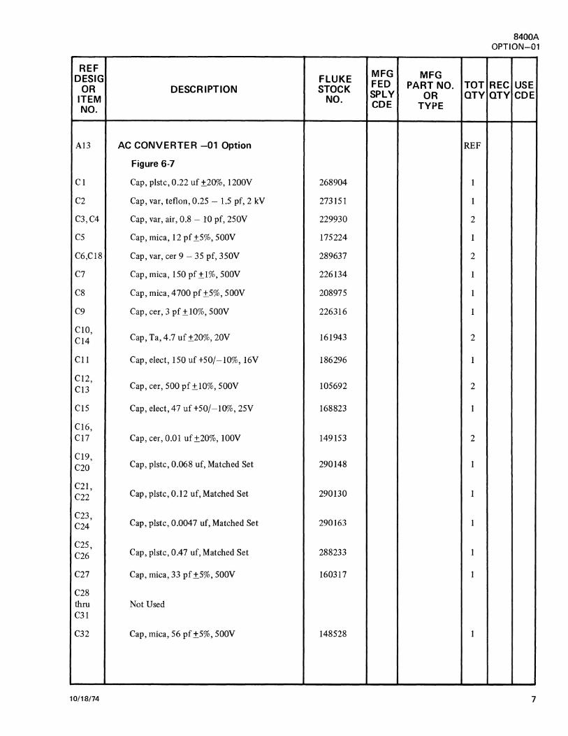
REF DESIG
OR DESCRIPTION ITEM NO.
Al3 AC CONVERTER -01 Option
Figure 6-7
Cl Cap, piste, 0.22 uf ±20%, 1200V
C2 Cap, var, teflon, 0.2S - 1.S pf, 2 kV
C3,C4 Cap, var, air, 0.8 - 10 pf, 2SOV
cs Cap, mica, 12 pf ±S%, SOOY
C6,C18 Cap, var, cer 9 - 3S pf, 3SOV
C7 Cap, mica, 1 SO pf ±1 %, SOOY
C8 Cap, mica, 4 700 pf ±S%, SOOY
C9 Cap, cer, 3 pf ±10%, SOOY
ClO, Cap, Ta, 4.7 uf ±20%, 20V C14
Cll Cap, elect, ISO uf +S0/-10%, 16V
C12, Cap, cer, SOO pf ±10%, SOOY Cl3
ClS Cap, elect,47 uf+S0/-10%, 2SV
C16, C17 Cap, cer, O.Ql uf±20%, lOOV
C19, Cap, piste, 0.068 uf, Matched Set C20
C21, Cap, piste, 0.12 uf, Matched Set C22
C23, Cap, piste, 0.0047 uf, Matched Set C24
C2S, Cap, piste, 0.47 uf, Matched Set C26
C27 Cap, mica, 33 pf ±S%, SOOY
C28 thru Not Used C31
C32 Cap, mica, S6 pf ±S%, SOOY
10/18/74
MFG MFG FLUKE STOCK FED PART NO.
NO. SPLY OR COE TYPE
268904
2731Sl
229930
17S224
289637
226134
20897S
226316
161943
186296
10S692
168823
1491S3
290148
290130
290163
288233
160317
148S28
TOT QTY
REF
1
1
2
1
2
1
1
1
2
1
2
1
2
1
1
1
1
1
1
8400A OPTION-01
REC USE QTY COE
7

8400A OPTION-01
REF DESIG
OR ITEM NO.
CRl thru CR4, CRIS
CRS, CR6
CR7, CR8, CR9 CRlO thru CR14 CR16
Kl
K2,K3 K6
K4,K5
QI
Q2,Q6
Q3,Q4, Q5,Q7
Rl
R2
R3
R4
RS, R32
R6
R7
R8
R9
8
DESCRIPTION
Diode, silicon, 100 mA at 1.SV
Diode, silicon, 100 mA at 1.SV
Diode, silicon, 150 mA
Diode, germanium, 80 mA, 100 piv
Diode, zener, 13V
Relay reed switch
Coil, relay
Relay, reed switch
Coil, relay
Relay, reed switch
Coil, relay
Tstr, FET, N-channel
Tstr, silicon, NPN
Tstr, silicon, PNP
Res, met fun, 1.1 lM l Matched Set Res, met fun, 267k
Res, var, cermet, 2k ±.10%, lw
Res, ww, 29.53k ±.0.1%, hw
Res, var, cermet, 200 ±.10%, 1 w
Res, ww, 2.573k±.0.1%, hw
Res, var, cermet, 20 ±.20%, lw
Res, ww, 143.3 ±.0.1%, %w
Res, met flm,49.9k±.1%, 1/8w
MFG MFG FLUKE STOCK FED PART NO. TOT REC USE
NO. SPLY OR QTY QTY COE COE TYPE
261370 5
161810 2
203323 3
149187 5
110726 1
284091 1
269019 3
219097 8
272070 3
219097 REF
269019 REF
246066 1
218081 2
229898 4
269092 1
285163 1
277657 1
285148 2
277665 1
285114 1
292193 1
268821 1
10/18/74
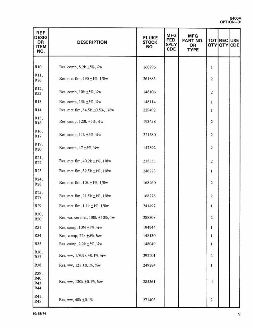
REF DESIG FLUKE
OR DESCRIPTION STOCK ITEM NO. NO.
RIO Res, comp, 8.2k ±5%, %w 160796
Rl 1, R26 Res, met flm, 590 ±1 %, 1/8w 261883
R12, Res, comp, IOk ±5%, %w R33 148106
R13 Res, comp, 15k ±5%, %w 148114
R14 Res, met flm, 84.Sk ±0.5%, 1/8w 229492
Rl5, Res, comp, 120k±5%, %w R18 193458
R16, Res, comp, 1 lk ±5%, %w R17 221580
R19, Res, comp, 47 ±5%, %w R20 147892
R21, Res, met flm,40.2k±1%, 1/8w R22 235333
R23 Res, met flm, 82.Sk ±1%, 1/8w 246223
R24, Res, met flm, IOk ±1%, 1/8w R28 168260
R25, Res, met flm, 21.5k±1%, 1/8w R27 168278
R29 Res, met flm, l.lk ±1%, 1/8w 241497
R30, Res, var, cermet, IOOk ±10%, lw R50 288308
R31 Res, comp, IOM ±5%, %w 194944
R34 Res, comp, 22k ±5%, %w 148130
R35 Res, comp, 2.2k ±5%, %w 148049
R36, Res, ww, 1.702k±0.1%, %w R37 292201
R38 Res, ww, 125 ±0.1%, %w 249284
R39, R40,
Res, ww, 130k ±0.1%, %w R43, 285361
R44
R41, Res, ww, 40k±0.1% R45 271403
10/18/74
MFG MFG FED PART NO. SPLY OR COE TYPE
TOT QTY
1
2
2
1
1
2
2
2
2
1
2
2
1
2
1
1
1
2
1
4
2
8400A OPTION-01
REC USE QTY COE
9

8400A OPTION -01
REF DESIG
OR ITEM NO.
R42, R46
R47
R48
R49
R51
R52
U1
U2
U3
U4
DESCRIPTION
Res, ww, lM.±0.1%
Res, var, cermet, lOk ±10%, lw
Res, met fun, 100 ±1%, 1/8w
Res, met flm, 487k ±1%, 1/8w
Res, comp, 9.lk±5%, ¥iw
Res, comp, lk±5%, ¥iw
IC, 5 transistor array
IC, operation amplifier
IC, DTL, triple 3-Input Nand Gate
IC, DTL, Quad 2-Input Nand Power Gate
Socket, IC, 14 contact, Ul, U3, U4
6-39. SERIAL NUMBER EFFECTIVITY
A Use Code column is provided to identify certain parts that have been added, deleted, or modified during production of the Model 8400A. Each part in this option for which a use code has been assigned may be identified with a particular printed circuit board serial number by consulting the Use Code Effectivity List below. All parts with no code are used on all printed circuit boards with serial
10
MFG MFG FLUKE FED PART NO. TOT REC USE STOCK SPLY OR QTY QTY COE NO. COE TYPE
271411 2
285171 1
168195 1
237206 1
193318 1
148023 1
248906 1
288928 1
266312 1
288597 1
276527 3
numbers 123 and on. NOTE: These Use Codes and Serial Number Effectivity apply to this option printed circuit board assembly only. For the standard instrument configuration, see Section 5, paragraph 5-9, and for additional options, see the appropriate option subsection.
USE SERIAL NUMBER EFFECTIVITY CODE
10/18/74

Figure 6-7. AC CONVERTER PCB ASSEMBLY
10/18/74
8400A OPTION -01
11 /12


6-1. INTRODUCTION
6-2. The Ohms Converter (Option -02) is used in conjunction with the basic DVM to provide resistance measuring capability in seven ranges: 10, 100, 1000, and 10000 ohms, and 100, 1000, and 10000 kilohms.
6-3. SPECIFICATIONS
64. Specifications for the ohms converter are located in Section 1, Introduction and Specifications.
6-5. INSTALLATION
6-6. Ohms Converter installation procedures are as follows:
a. Disconnect the power cord from line power.
b. Remove the top dust and guard chassis covers. On the A14 Display motherboard in the instrument, determine that connector J12 is clear of obstructions and that the alignment spacer is inserted between pin pairs Jl2-8, -9 and Jl2-10, -11 (see Drawing No. 8400A-1002, Sheet 1 of 2). Locate terminal block No. 1, terminals P3TF and P3TR, and connect the yellow and brown wires from the Ohms Converter board to these terminals, respectively. Layout other cable attached to rear of Al 2 Ohms Converter along inside bottom of the DVM chassis, underneath the other circuit boards, and emerge adjacent to terminal block No. 2. Attach to terminal block No. 2 terminals as shown on the wiring diagram, Drawing No. 8400A-1000. Also see terminal block layout diagram on guard cover.
c.
d.
6-7.
8400A OPTION-02
Option-02
Ohms Converter
Align converter board vertically with plastic guide slots on inner vertical faces of guard chassis. Align rubber grommet with slot in front guard chassis and insert. Slide converter board downward to fully engage card-edge connector with Jl 2 connector on motherboard.
Attach guard and instrument dust cover, connect ac power, and perform receiving inspection test of converter as described in paragraph 6-27, Performance Test.
OPERATING INSTRUCTIONS
6-8. Operation of the DVM with the Al2 Ohms Converter Option 8400A-02 installed is covered in Section 2, Operating Instructions.
6-9. THEORY OF OPERATION
6-10. General
6-11. The Ohms Converter is operated in one of two configurations associated with the functions of Ohms and K ohms. In the n function, the ohms converter is a constant current source which is connected to the SOURCE Terminals on the front panel of the 8400A. In K n function the ohms converter is a precision scaling resistor, which, in conjunction with the Buffer amplifier located in the basic instrument, and the unknown resistor, produces a voltage proportional to the unknown resistor. Simplified diagrams are shown in Figure 6-1.
6-12. n CONFIGURATION. A constant current is supplied to the HI and LO SOURCE Terminals of the

8400A OPTION-02
8400A from a current source as shown in Figure 6-1. A regulated de voltage supplies a fixed current to a reference zener diode. The zener reference voltage is impressed across a precision resistor causing a current to flow into the emitter of a transistor. Because this transistor is a high gain device, the majority of the emitter current flows out of the collector, hence, out of the HI SOURCE terminal. The LO SOURCE terminal provides a return path for the precision current.
6-13. The constant current generator produces one of three currents dependent upon the range selected. Table 6-1 shows the current generated for each range selected on the front panel of the 8400A.
Table 6-1. CURRENT OUTPUT, n CONFIGURATION
OHMS RANGE CURRENT
CALLED CALLED
10 10 ma
100 10 ma
1000 1 ma
10K 100µa
6-14. True four-terminal resistance measurements can be made in the ohms function. The term true four-terminal is used because the current generator is completely isolated from the remaining circuitry in the instrument, and hence, no current will flow in the voltage sense terminals even in the presence of relatively large lead resistances.
6-lS. Kil CONFIGURATION. In the Kn function, a range dependent scaling resistor is placed between the master +7 volt reference and the HI SOURCE terminal. A voltage proportional to the unknown resistance (Rx) is available at the buffer output as shown in Figure 6-1.
6-16. Circuit Description
6-17. CONSTANT CURRENT GENERATOR. Regulated de voltage is developed by resistors R2, R4, RS, zener diode CR3, transistor Ql and operational amplifier UL Divider string, R6, R7, and R8, scales the zener reference voltage and applies it to U2. Range resistors RlO through Rl6, in conjunction with zener CR3, the regulated de voltage, and amplifier U2, apply a range dependent, constant current to the emitter of a Darlington pair composed of Q2 and Q3. Fuse F 1, capacitor C6, and diodes CR2, CR4 are used as an overvoltage protection circuit for the current generator.
2
OHMS
KILOHMS
LO SENSE
Eo~-(R SCALING) Rx
"'>---'-----\ OUTPUT TO ACTIVE FILTER
Figure 6-1. SIMPLIFIED DIAGRAM OF OHMS CONVERTER SHOWING TWO CONFIGURATIONS
6-18. RANGE SCALING NETWORK. Resistors Rl 7 through R22, and relay contacts Kl-A, K2-A and K4 are the range scaling network. The relay contacts Kl-A and K2-A are actuated by range selection on front panel. Relay K4 is actuated in the Kn function and connects one end of the scaling networ~ to the HI SOURCE terminal on front panel.
6-19. RELAY DRIVE CIRCUIT. Range control relay Kl receives its call commands from the All BUFFER assembly, whereas relay K2 receives its call commands from the buffered A14 range counter. Function control relays K3 and K4 are controlled by transistors Q6 and QS, respectively. A manual range condition is detected by Gate USB which enables gates USC and USD to control QS and Q6. In an autorange condition, gates USC and USD are disabled and function control is transferred by gate U3B to RS flip-flop U3A and U3C. The mutually exclusive outputs of this flip-flop, in turn, control switches QS and Q6. Gates U4A and U4B operate on the set and reset lines of the RS flip-flop to enable an automatic change of functions in an autorange condition.
6-20. MAINTENANCE
6-21. Introduction
6-22. This section contains maintenance information for the Ohms Converter. Factory service information and general instructions regarding instrument access and cleaning are located in Section 4 of the manual.

6-23. Test Equipment
6-24. The resistance valves for performance testing, troubleshooting, and calibration of the Ohms Converter is listed in Table 6-2.
Table 6-2. REQUIRED RESISTANCE VALVES
STANDARD RESISTANCE TOLERANCE
VALVE
10.Q ±30 PPM 100.Q ±30 PPM
1K.Q ±20 PPM 10K.Q ±20 PPM
100K.Q ±20 PPM 1M.Q ±20 PPM
10M.Q ±100 PPM
6-25. Fuse Replacement
6-26. The Ohms Converter contains two fuses, one of which prevents damage in the event large ac or de voltages are inadvertantly applied to the DVM input during ohms operation. The circuit will withstand a maximum applied voltage of 20 volts rms on 10.Q through 10,000.Q range before the fuse will blow. Up to 250V rms may continuously be applied to the 1 OOk.Q through 10,000k.Q ranges without damage. A spare fuse is located on the ohms converter pcb, next to the in-circuit fuse.
6-27. Performance Tests
6-28. The performance tests in this section compare the Ohms Converter performance to the accuracy specifications in Section 1 of the manual to determine if the converter is in calibration. Appropriate resistance standards are connected to the input on each ohms range. The performance tests should be conducted before any instrument maintenance or calibration is attempted. The tests are also suited to receiving inspection of new converters. Performance tests should be conducted under the following environmental conditions: Ambient Temperature 23°C ± 5°C, Relative Humidity less than 70%. An instrument that fails any of the performance tests will require corrective maintenance or calibration. In case of difficulty, analysis of the test results, with reference to the troubleshooting section, should help to locate the trouble.
10/18/74
8400A OPTION-02
NOTE!
Permissible tolerances for resistance measurements are derived from the 90-day instrument specifications tained in Section I of the manual.
6-29. KILOHMS TEST. The kilohms function is checked at full scale on each of three ranges of the DVM. Connect each of the standard resistors shown in Table 6-3, in turn, to the INPUT terminals of the Model 8400A. Use short, low-resistance connecting leads. Set the DVM controls as shown in the table. The readout should be as indicated.
Table 6-3. KILOHMS TEST REQUIREMENTS
STANDARD MODELB400A
RESISTANCE FUNCTION RANGE READOUT LIMITS
100Kil Kil 100 99.988 to 100.012
1000Kil Kil 1000 999.88 to 1000. 12
10Mil Kil 10K 9994.8 to 1005.2
6-30. OHMS TEST. The ohms function is checked at full scale on each of four ranges on the DVM. Connect equipment as shown in Figure 6-2. Connect each of the standard resistors in Table 6-4, observing appropriate readout as indicated.
(8400A)
INPUT .QsENSE
GD
n SOURCE
Figure 6-2. EQUIPMENT CONNECTIONS FOR OHMS TEST
Table 6-4. OHMS TEST REQUIREMENTS
STANDARD MODEL8400A RESISTANCE FUNCTION RANGE READOUT LIMITS
10.n .n 10 9.9980 to 10.0020
1oo.n .n 100 99.987 to 100.013
1Kil .n 1000 999.87 to 1000.13 10Kil .n 10K 9998.7 to 10001.3
3

8400A OPTION-02
6-31. Calibration
6-32. The Ohms Converter should be calibrated every 90 days to maintain specifications (see specifications, Section 1 ), or whenever repairs have been made to circuitry. Calibration of the converter should be performed at an ambient room temperature of 23 ±.5°C. Relative Humidity should be less than 70%. Consult Table 6-2 for recommended test equipment.
6-33. PRELIMINARY OPERATIONS
a. Remove the upper dust cover retaining screws, but leave the dust cover in place on the instrument.
b. Set the rear panel 115/230 volt slide switch to the 115 volt position and connect the line cord to an autotransformer set to 120 volts ac.
c. Turn on the Model 8400A and allow the instrument to operate for one hour.
d. Remove the upper dust cover and set the Model 8400A controls as follows:
FUNCTION VOC,FILT
RANGE .1
SAMPLE RATE full clockwise
e. Connect the GUARD terminal to the LO INPUT terminal and the HI SOURCE terminal to the HI INPUT terminal, and the LO SOURCE terminal to the LO INPUT terminal using the shorting links provided with the instrument.
f. Short the INPUT terminals together.
g. Adjust the OC ZERO control on the front panel for a zero ±1 digit.
6-34. KILOHMS CALIBRATION
a. Depress lOK and KQ buttons.
b. Remove the short between the INPUT terminals.
c.
4
Connect the resistances indicated in Table 6-5 between the INPUT terminals and perform the corresponding adjustment.
Table 6-5. KQ RANGE CALIBRATION
RESISTANCE RANGE ADJUSTMENT READOUT
10M
1M
100K
10K 10000K (A12R171
1000 1000K (A12R19)
100 100K (A12R21)
NOTE!
The readout indicated in Table 6-5 should match the exact value of the calibration resistor, not the nominal value.
10000.0
1000.00
100.000
6-35. OHMS CALIBRATION
a. Remove shorting links between the INPUT HI and
SOURCE HI binding posts, and between INPUT LO and SOURCE LO binding posts.
b.
c.
d.
Connect equipment as shown in Figure 6-2.
Depress Q and 1 OK buttons on Model 8400A.
Connect the resistance indicated in Table 6-6 as shown in Figure 6-2 and perform the corresponding adjustment.
Table 6-6. OHMS RANGE CALIBRATION
STANDARD RANGE ADJUSTMENT READOUT
10K 10K 100<>00 (A12R7) 10000.0
1K 1000 1ooon !A 12R 141 1000.00
1oon 100 100flA12R101 100.000
1on 10 NONE 10.000 ±..006*
NOTE* IF MORE THAN ±..006 RESET voe ZERO AND
RECALIBRATE OHMS RANGES
e. Re-install shorting links.
6-36. Calibration of the Ohms Converter is now cqm
plete.
6-37. TROUBLESHOOTING
6-38. Introduction
6-39. This section contains information selected to aid in troubleshooting the Ohms Converter. Before any
10/18/74

attempt is made to troubleshoot the converter, however, it should be verified that the trouble is actually in the converter and not caused by faulty external equipments or improper control settings. For this reason, the performance tests (paragraph 6-27) are suggested as a first step in troubleshooting. The performance tests may also help to localize the trouble to a particular section of the converter. If the performance tests fail to localize the trouble, the following information may be helpful.
6-40. TROUBLESHOOTING
a.
b.
Depress Kn, FIL T and JOOO buttons on Model 8400A.
Place a 1 meg ± .01 % resistor across the INPUT terminals and readout J000.00±.10.
------FAULT ANALYSIS-----
IF READOUT IS BAD, FAULT MAY BE IBE REFERENCE VOLTAGE OR Rl7, Rl8, Rl9, R20 OR RELAY Kl.
c. Depress JOO button.
d. Place a JOOk ±.01 % resistor across INPUT terminals and readout JOO.ODO ±.010.
,,,_. _____ FAULT ANALYSIS-------.
e.
f.
IF READOUT IN STEP d. IS BAD, FAULT MAY LIE IN RESISTORS R21 OR R22 OR RELAY K2
Depress n and JOOO buttons.
Measure a JOOO ±.01 % resistor using the fourterminal measurement technique (see Figure 6-2).
g. Readout 1000.00 ±.10.
------FAULT ANALYSIS-----..
IF READOUT IS BAD, RESISTOR NETWORK RIO, R11, R12 OR REGULATED SUPPLY, OR K2 MAY BE FAULTY.
h. Depress JOO button.
i. Using modified four-terminal technique measure 100 ± .01 % resistor.
j. Readout J00.000 ±.010.
8400A OPTION-02
...------ FAULT ANALYSIS-----..
IF READOUT IS BAD, RELAY Kl OR RESISTORS R13, R14, RlS, R16 OR REGULATED SUPPLY MAY BE FAULTY
6-41. LIST OF REPLACEABLE PARTS
6-42. For column entry explanations, part ordering information and basic instrument configuration Use Codes and Serial Number Effectivity List, see Section 5, paragraphs 5-1 through 5-10. See paragraph 6-43, this option subsection, for additional Use Codes and Serial Number Effectivity List assigned to this printed circuit assembly option.
6-43. SERIAL NUMBER EFFECTIVITY
6-44. A Use Code column is provided to identify certain parts that have been added, deleted, or modified during production of the Model 8400A. Each part in this option for which a use code has been assigned may be identified with a particular serial number by consulting the Use Code Effectivity List below. All parts with no code are used on all serial numbers 123 and on. NOTE: These Use Codes and Serial Number Effectivity apply to this option only. For the standard instrument configuration, see Section 5, paragraph 5-9, and for additional options, see the appropriate option subsection.
USE CODE
A
B
SERIAL NUMBER EFFECTIVITY
123 thru 73399
73400 and on
10/18/74 5
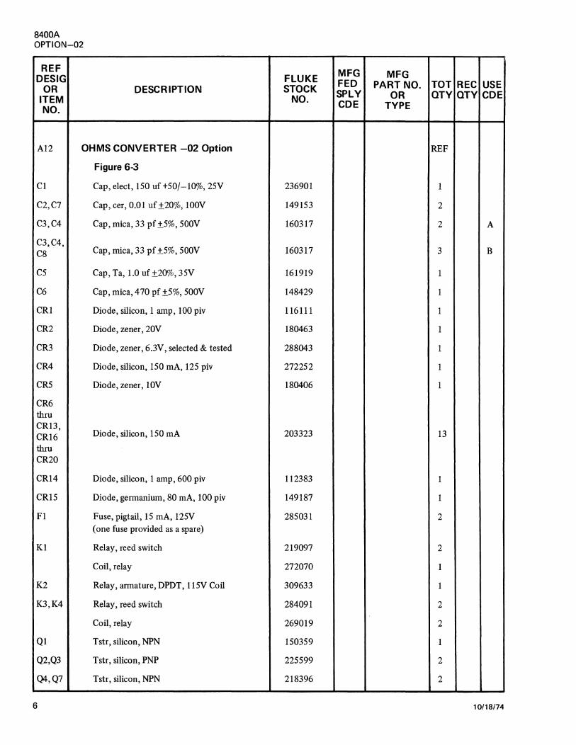
8400A OPTION-02
REF DESIG
OR ITEM NO.
DESCRIPTION
A12 OHMS CONVERTER -02 Option
Figure 6-3
Cl Cap, elect, ISO uf +S0/-10%, 2SY
C2,C7 Cap, cer, 0.01 uf±20%, lOOY
C3,C4 Cap, mica, 33 pf ±S%, SOOY
C3,C4, Cap, mica, 33 pf ±S%, SOOY C8
cs Cap, Ta, 1.0 uf ±20%, 3SY
C6 Cap, mica, 4 70 pf ±S%, SOOY
CRI Diode, silicon, 1 amp, 100 piv
CR2 Diode, zener, 20Y
CR3 Diode, zener, 6.3Y, selected & tested
CR4 Diode, silicon, ISO mA, 12S piv
CR5 Diode, zener, IOY
CR6 thru CR13,
Diode, silicon, ISO mA CR16 thru CR20
CR14 Diode, silicon, 1amp,600 piv
CRIS Diode, germanium, 80 mA, 100 piv
Fl Fuse, pigtail, lS mA, 125V (one fuse provided as a spare)
Kl Relay, reed switch
Coil, relay
K2 Relay, armature, DPDT, 11 SY Coil
K3,K4 Relay, reed switch
Coil, relay
Ql Tstr, silicon, NPN
Q2,Q3 Tstr, silicon, PNP
Q4,Q7 Tstr, silicon, NPN
6
MFG MFG FLUKE STOCK FED PART NO. TOT REC USE
NO. SPLY OR QTY QTY COE COE TYPE
REF
236901 1
1491S3 2
160317 2 A
160317 3 B
161919 1
148429 1
116111 1
180463 1
288043 1
2722S2 1
180406 1
203323 13
112383 1
149187 1
28S031 2
219097 2
272070 1
309633 1
284091 2
269019 2
1S03S9 1
22SS99 2
218396 2
10/18/74

REF DESIG
OR DESCRIPTION ITEM NO.
Q5,Q6 Tstr, silicon, PNP, selected
QB Tstr, silicon, PNP
Rl,R9 Res, comp, lOk ±5%, %w R29
R2,R4 Res, met flm, lOk ±1%, l/8w
R3 Res, comp, 2.2k ±5%, %w
RS Res, met flm, 953 ±1%, %w
R6 Res, met flm, 619k ±1%, l/8w
R7, RI9 Res, var, cermet, lk ±20%, ~w
R8, Res, var, cermet, 25k ±20%, )2w Rl7
RIO Res, var, cermet, lOk ±20%, )2w
RI I Res, met flm, 46.4k ±1%, I /8w
R12 Res, ww, 634.13 ±0.05%, %w
R13 Res, met flm, 464k±1%, I/8w
Rl4 Res, var, cermet, lOOk ±20%, ~w
RI5 Res, ww, 6.983k ±0.05%, %w
R16 Res, ww, 62k ±0.05%, %w
R18 Res, met flm, 6.99M ±0.1%, 2w
R20 Res, ww, 777.15k ±0.05%, 3/4w
R21 Res, var, cermet, 100 ±20%, )2w
R22 Res, ww, 70.555k ±0.05%, ~w
R23 Res, met flm, 100 ±1%, 1/8w
R24, Res, comp, 390 ±5%, %w R25
R26 Res, comp, 8.2k ±5%, %w
R26, Res, comp, 8.2k ±5%, %w R34
R27 Res, comp, 4.7k ±5%, %w
R28 REs, comp, lk ±5%, %w
10/18/74
MFG MFG FLUKE STOCK FED PART NO.
NO. SPLY OR CDE TYPE
280198
195974
148106
168260
148049
288555
288639
267856
285213
267880
188375
292888
271908
268581
292896
292904
284968
277913
267823
277905
168195
147975
160796
160796
148072
148023
TOT QTY
2
1
3
2
I
I
1
2
2
1
I
1
1
1
1
1
I
1
1
I
1
2
1
2
1
1
8400A OPTION-02
REC USE QTY COE
A
B
A
7

8400A OPTION-02
REF DESIG
OR ITEM NO.
R28, R33
R30, R31
R32
Ul
U2
U3
U4
us
8
FLUKE DESCRIPTION STOCK
NO.
Res, comp, lk ±.S%, %w 148023
Res, comp, S60 ±.S%, ~w 147991
Res, comp, 220 ±.S%, ~w 1479S9
IC, operational amplifier 271S02
IC, operational amplifier 284760
IC, DTL, triple 3-Input Nand Gate 266312
IC, DTL, dual 4-Input Nand 268383
IC, DTL, Quad 2-Input Nand Gate 26837S
Fuse holder 296S82
Socket, IC, 14 contact, U3, U4, US 276S27
MFG MFG FED PART NO. TOT REC USE SPLY OR QTY QTY COE COE TYPE
2 B
2
1
1
1
1
1
1
2
3
10/18/74

Figure 6~3. OHMS CONVERTER PCB ASSEMBLY 10/18/74
8400A
OPTION - 02
9/10

6-1. INTRODUCTION
6-2. The Data Output Unit (Option-03) provides data output that is completely isolated from the analog input and is available in 8-4-2-1 BCD logic level format. Data is
transferred serially via guarded toroids from the Model 8400A to the Data Output Unit. Single decade code conversion and serial-character, parallel-bit acquisitions are unique capabilities, in addition to standard full parallel output.
6-3. SPECIFICATIONS
6-4. Specifications for the Data Output Unit are loca-ted in Section 1 of the manual.
6-5. INSTALLATION
6-6. The following procedure should be used to install the Data Output Unit in the Model 8400A.
a. Disconnect the power cord from the instrument before installing the Data Output Unit option.
b. Remove the top dust and guard chassis covers.
c.
d.
Determine that connector 17, on A14 Display board, is clear of obstructions and that alignment spaceris inserted between pin pairs 17-1, -2 and 17-3, -4. A second alignment spacer must be inserted between pin pairs 17-21, -22 and 17-23, -24.
Determine that connector slots on rear panel for P20 and P21 on Data Output Unit boards are clear of any obstructions.
e.
f.
g.
h.
i.
j.
j.
k.
6-7.
8400A OPTION-03
Option-03
Data Output Unit
Attach spring to bottom portion of guard bar on A 7 Data Output Unit No. 1.
Insert P21, on A 7 Data Output Unit No. l, into connector slot on rear panel while inserting P20 on A6 Data Output Unit No. 2 into rear panel connector slot. (Refer to Section 5, Figure 5-1 for physical location of A 7 and A6)
Insert edge of both the Data Output Units (A6 & A 7) into card guides on the inner chassis bulkhead.
Observe that alignment spacers on 17 line up with slots on the Data Output Unit card-edge connector.
Slide both boards downward until the card-edge connector on A7 is fully engaged with 17 on A14 Display board, and A6 is seated into bracket.
Lay the twisted pair cable under the top position of the rear panel and route toward transformer.
Connect wires to jacks mounted on transformer so yellow mates to yellow and blue to blue.
Attach guard and dust covers, connect ac power, and perform receiving inspection test of the Data Output Units as described in paragraph 6-33, Performance Test.
OPERATING INSTRUCTIONS
6-8. Operating instructions and applications information for the Model 8400A with DOU installed are located in Section 2 of the manual.
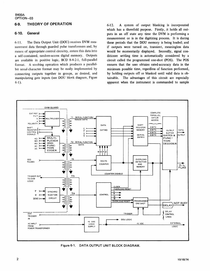
8400A OPTION-03
6-9. THEORY OF OPERATION
6-10. General
6-11. The Data Output Unit (DOU) receives DVM measurement data through guarded pulse transformers and, by means of appropriate control circuitry, enters this data into a self-contained, random-access digital memory. Outputs are available in positive logic, BCD 8-4-2-1, full-parallel format. A strobing operation which produces a parallelbit serial-character format may be easily implemented by connecting outputs together in groups, as desired, and manipulating gate inputs (see DOU blovk diagram, Figure 6-1).
DVMGUARD ---------~
I EXT REF
FILT
a POLARITY
SHIFT { REGISTER
I ! I Tl SERIAL FUNCTION/ RANGE DATA
I t-
MULTIPLEXER
CONTROL >----. SIGNALS
Kr! Mr! MV AC DC
MULTI· PLEXER AND FUNCTION CODER
11
~~ .. ~II ~~l~~~ROU~l I T5
'"" s----1 + -r SYNCH RO-
I I M NIZATION
CIRCUIT
--------------EXT TRIGGER IN
AC INPUT FROM POWER TRANSFORMER
T4
5,___.,.
SERIAL FUNCTION
DATA
+5 voe LOGIC
SUPPLY
DATA
6-12. A system of output blanking is incorporated which has a threefold purpose. Firstly, it holds all outputs in an off state any time the DVM is performing a measurement or is in the digitizing process. It is during these periods that the DOU memory is being loaded; and if outputs were turned on, transient, meaningless data would be momentarily displayed. Secondly, signal conditioner settling time is automatically considered by a circuit called the programmed one-shot (POS). The POS ensures that the user obtains rated-accuracy data in the minimum possible time, regardless of function performed, by holding outputs off or blanked until valid data is obtainable. The advantages of this circuit are especially apparent when the instrument is commanded to sample
COMPLETE PARALLEL
DATUM ACCESS
8 BITS
GATING
SHIFT REGISTER MEMORY 8 BITS OUTPUT DATA
WXYZ
DIGITS
COUNTER
COUNTER DISABLE
CONTROL
TRIGGER
~ ~,...--...,•• DOU LOGIC
!SERIAL ENTRY)
OVERLOAD
8 BITS BUFFER
.......... a_..B-.IT-...S _.,.GATES & FUNCTION DECODER
UT PUT
oE;~gTION t---e---o. L. FLAG MEMORY
+5 voe
{
DELAY
CONTROL LINES
EXTERNAL
LOGIC ..
Figure 6-1. DATA OUTPUT UNIT BLOCK DIAGRAM.
2 10/18/74

upon simultaneous application of a transient signal or step change to the DVM input. The POS holds outputs off just Jong enough for the signal conditioner in use to settle to rated accuracy. When a different signal conditioner is called in to operation by the user, the POS automatically adjusts timeout delay to the new conditions. At timeout, the POS triggers a new measurement before turnmg on the outputs 23 milliseconds later. Thirdly, automatic tanging is detected by the OOU, and data outputs are blanked during operations associated with that function. After the blanking process is complete, the outputs will remain on and unchanged until the DVM is again commanded to sample.
6-13. Following is an example of a typical sequence of internal events as initiated by a user-generated sample com
mand.
a. An unknown input and a trigger (command to sample) are applied simultaneously to the DVM.
b. The POS reverts to its unstable state, thereby inhibiting all outputs.
c. The DVM makes a preliminary measurement, (requiring 6 milliseconds) to determine if ranging is necessary.
d. Autoranging takes place and the timeout is increased by 250 milliseconds for each range change.
e.
f.
h.
The programmed one-shot begins to time out in accordance with the function delay data registered in the DOU memory.
At the end of the required settling time, the DVM is automatically commanded to sample again by the POS as it reverts to its stable state.
New data is registered in the DOU memory as a result of this final sample.
All the outputs are then turned on to provide function, range, polarity, and specified-accuracy numerical data. A ready flag indicates whether outputs are on or off.
6-14. Circuit Description
6-15. LOGIC NOTATION. A description of the logic symbology used in the DOU is given in Figure 6-2. A J-K flip flop that is in the "l" condition or is set "high" has a
8400A OPTION-03
"high" output from the "Q" terminal. The orientation of the flip flops in the schematics is the same as the flip flops shown in Figure 6-2. This method of notation enables input/output terminals of the flip flops to be identified without the necessity of redundant lettering of each device symbol. In the main, the routing of logic and control signal on the schematics is accomplished without connecting lines, which greatly reduces conjestion.
6-16. MULTIPLEXERS. The DVM function, range, and polarity inputs are applied t1J dual multiplexer 1:ircuitr~
consisting of NAND gates A 7U27 A through D, A 7U28A through D, A7U29C and A7U29D, (see DOU schematic at rear of manual). The gates comprising each multiplexer are enabled sequentially by the 6-state shift register signals. The multiplexer outputs are applied to inverter circuits consisting of NOR gates A 7U31A, A 7U3 ID, A 7U31 E, A 7U3 l F, and transformers Tl and T2. The pulses produced by Tl and T2 secondaries are applied to RS flip flops composed of inverters A7Ul3A, A7U13B, A7U13D, A7Ul3E, which reconstruct the multiplexer inputs for application to the data gates. Examples of the RS flip flop outputs are
shown in the timing diagram of Figure 6-3 (signals 13-8 and 13-4) and correspond to the following DVM functions and input conditions: VDC function with filter called, 1 range, negative voltage applied to input and remotely controlled. A complete list of waveforms appearing at the output of the RS flip flops is given in the troubleshooting section. (See Figure 6-9). Waveforms are labeled according to circuit
location (e.g., 13-4 means I. C. Ul3 pin 4).
6-17. DIGITS COUNTER. The digits counter consists of J-K flip flops A6U26A, A6U26B, A6U25A and A6U25B. The input flip flop, A6U25A is toggled by positive pulses, which are transferred through the guard by A 7U3 2C and transformer T3. The counter produces a 4-bit binary output that is entered into the memory via the data gates. The counter is reset at the beginning of each sub-period of the measurement cycle by the F signal. The W, Y, and Z counter outputs are also applied to NAND gate A6U22A, which stops the counter at a count of "11" and generates a high at the input of flip flop A6U21B. If another pulse appears at the secondary of T3, it is indicative of "12" in the first decade (i.e., instrument overload). The 12th pulse toggles flip flop A6U21 B to produce an overload indication at the DOU output, A7P20-13.
6-18. DAT A GATES. The data gates consist of NAND gates A 7U22C, A 7U23A through U23C, and A 7U24A through U24D. The gates are controlled by the F, F, S, and S signals so that the 10 bits of function, range, and polarity data and 20 bits of numerical data are presented to
3

8400A OPTION-03
LOGIC SYMBOL NAME DESCRIPTION
J-K Flip Operation of the J-K flip flop is shown by the following truth tables.
i Flop Note that "S" and "R" inputs are dominant over "J" and "K" inputs.
SYNCHRONOUS ASYNCHRONOUS INPUTS INPUTS
J----, ~Q
c- t--0 J K On+1 s R Q l a K-
1 0 0 On 0 0 Undefined
0 1 0 0 1 ~Set R 1 0 1 1 0 Reset
1 1 an 1 1 Normal Condition
~::[>---NOR The following table shows gate and inverter operation. Although Gate only two-input gates are shown, operation is identical for gates
having additional inputs.
~=r=r NANO Gate A B NOR NANO INVERTER
0 0 1 1 1
A-{>o- Inverter 0 1 0 1 1
1 0 0 1 0
1 1 0 0 0
CLOCK Four B-bit, serial-in parallel-out shift registers are used. A logical +SV PULSE "1" at the input enters a logical "1" into the register. l l
Shift Register
~ S~RIAL INPUT
Figure 6-2. EXPLANATION OF LOGIC SYMBOLOGY USED IN DOU
the shift register memory at the proper times. These data bits are loaded in accordance with the load sequence (see Figure 6-4) and are steered by the data gates.
6-19. RANDOM ACCESS MEMORY. The DOU memory is composed of shift registers A 7Ul 0, A 7Ul 2, A 7Ul 4 and A 7Ul 6. Data is loaded serially into the shift registers. The loading sequence is controlled by clock pulses which are produced by gates A 7Ul SA through U1 SD, gate A 7Ul 9B and associated circuitry. Steering signals, S and S, together with the loading signal, F, develop loading pulses as shown in Figure 6-3. NAND gate A7Ul9B, inverter A7U13C, and associated circuitry delay the F signal for approximately 10 microseconds so that all data present at the shift register inputs will be stabilized before clocking occurs.
4
6-20. CONTROL. F and F signals are produced by an RS flip flop consisting of NOR gates A7U19A, A7U19C and associated circuitry. The trigger for the flip flop is developed by inverters A7U31B and C, A7U32A, B, and E, and transformerT4. The F andF signals are conditioned by the F, M, and ZERO signals so that the F and F signals occur only during periods A through E of the DVM measurement cycle. The steering flip flop is triggered by the F signal
and produces S and S signals.
6-21. The S output of the steering flip flop is applied to transistor A6Q9 and associated components, which comprise a rechargeable one-shot. This circuit is responsible for initializing control circuit conditions and providing for generation of the M signal. The sequence of operation of the

8400A OPTION-03
rechargeable one-shot and associated circuitry is as follows (control timing signals are shown in Figure 6-3):
f. Gate A6Ul 7 A is inhibited, thereby inhibiting all output buffer gates.
a.
b.
c.
d.
e.
Measurement cycle is initiated. g.
RS flip flop A 7Ul 9 A, A 7Ul 9C is set to "1" condition (pin 2of19A high).
The steering flip flop is toggled (Middle of "A" period) and capacitor A6C14 begins to charge toward +SV.
h. Flip flop A6U20B, C is reset by F.
The steering flip flop is again toggled (Middle of "B" period) and capacitor A6C14 is quickly discharged to 0.9V.
Overload flip flop A6U21 B is reset by a measurement inclusion signal generated at pin 8 of flip flop A6U20B,C.
i. Steps (f) and (g) repeat for "C", "D", and "E" periods.
Measure/store flip flop (A6U20A, D) is set by overload reset signal (signal No. 21-10).
j. Following "E" period, A6C14 continues to charge until A6Q9 is turned on.
PERIOD
F' 19-2
OVERLOAD 20-8 RESET
"M' 20-3
RECHARGEABLE ONE-SHOT Cl4
s 21-6 ------"-----.
LOADPULSE 15-14----~
DATA 13-8
DATA 13-4
cco PULSES
O~~~~~AD 21-9 ------
AUTORANGE DETECTOR,
CAPACITOR C15
2.5
1.5 ,-0.5 I
AUTO-RANGING OPERATIONS
250 MS EACH RANGE CHANGE
A ---t-- B --+--- C --+I
c REM
FILTER - lRANGE
(-)POL -REMOTELY CONTROLLED voe
FLIP FLOP 20A TRIGGER THRESHOLD
CONDITIONS: voe AND FILTER FUNCTIONS CALLED 1 RANGE CALLED
NOTE:
-0.63512 VOLTS APPLIED TO INPUT REMOTELY CONTROLLED SIGNAL NUMBERS CORRESPOND TO NUMBERED I/C'S & PINS LOCATIONS ON DOU SCHEMATIC
Figure 6-3. DOU TIMING DIAGRAM
5

8400A OPTION-03
SHIFT -PIN3 REGISTER OUTPUT
SERIAL DATUM ENTRY
ENTRY TIMING
I I I
-MID "E"
RANGE CODE ~ lL .£..
10000 0 0 0 1000 0 0 1
100 0 0 10 0 1
1 1 0 0 0.1 1 0 1
PIN 4 PIN 5
' I I I
BEGIN MID BEGIN "E" "D" "D"
FUNCTION CODE 'Y O'. POL
voe 0 0 0 -voe 0 0 1
KD 0 1 0 n 1 0 0 VAe 1 1 0
PIN 6
I I I
MID "C"
PIN 10 PIN 11
I I I I I
BEGIN MID "C" "B"
NOTE:
PIN 12
I I I
BEGIN MID "B" "A"
PIN 13
BEGIN "A"
SHIFT .REGISTER
+ } 10
} 14
} 12
} 16
1. All data in the shift register memory is inverted. It is inverted to positive logic on passing through the output gates.
Figure 6-4. SHIFT REGISTER LOAD SEQUENCE
k.
1.
A6Q8 then turns on and sets the overload reset flip flop A6U20B, C and the steering flip flop (A6U21A).
The measure/store flip flop is reset by a negative trigger developed in the circuit of A6Q7.
m. The output buffer gates are enabled and the data becomes available.
6-22. In addition to providing a pseudo measure/store signal, the circuit of flip flop A6U20A, D and transistor A6Q7 also function as an autorange detector. Control signal timing under autorange conditions is shown in Figure 6-5. If the decision to autorange is made (middle of "A" period), the DVM logic places the DOU in storage mode. This locks out the F signal in the DOU control circuit and, consequently, no pulses are produced in T4 secondary, excepting the first. With no F signal to toggle flip flop A6U21B the rechargeable one-shot times out and sets the overload reset flip flop to the "l" condition. The resulting signal (signal 21-9) is applied as a reset pulse to A6Q7; however, because capacitor A6C 15 has not had time to discharge sufficiently, the trigger threshold of flip flop A6U20A, D is not reached and the flip flop remains in its previous state. Thus, the output buffer gates are inhibited during the
6
autorange operation. If the instrument had not autoranged, A6Cl4 would have acquired sufficient charge during the measurement cycle to enable flip flop A6U20A, D to be triggered, as shown in the timing diagram of Figure 6-3.
6-23. The programmed one-shot consists of NOR gates A6 Ul 8A, C, transistors A6Q3 through A6Q6, capacitor A6C9, and associated programming resistors. In its stable state, gate A6Ul 8C output is high and gate A6U l 8A output is low. Assume that an external trigger is applied to A6P20-3. The trigger enable gate A6Ul 8B, thereby triggering the DVM to initiate a measurement cycle. The trigger also enables gate A6Ul8C, and the POS then switches to its unstable state. When the POS switches states, the output of gate A6U18D goes low, resulting in gates A6Ul 7A being inhibited. Inhibiting gate A6Ul 7 A causes all of the output data gates to be inhibited.
6-24. The timeout of POS delay is initiated as soon as the circuit is triggered, i.e., when the POS is triggered, switch A6Q3 is turned off and A6C9 begins to charge through the programming network to zero volts. Delay time is controlled by the memory, which selects resistor A6R22, R42, R45, R46, R47, R48, R52, R53, R54, R56, R57, depending on the selected DVM function. When A6C9 has accumulated sufficient charge, transistors A6Q4
10/18/74
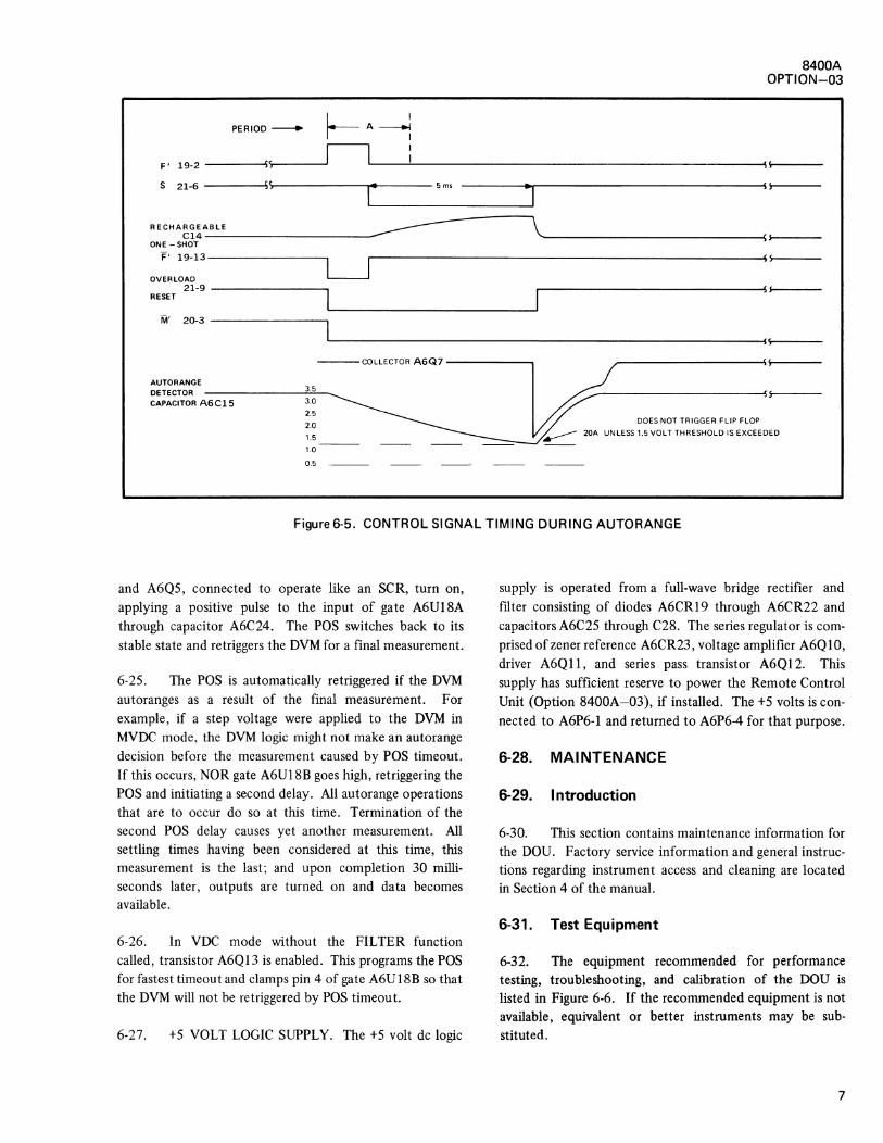
PERIOD-
F' 19-2 ----·---~
S 21-6 ---~,.,__ _____ ...,. ___ Sms
RECHARGEABLE Cl4------------
0NE-SHO.T
F' 19-13--------.
OVERLOAD 21-9 ------~
RESET
8400A OPTION-03
---COLLECTOR A6Q7 ----~
AUTO RANGE DETECTOR CAPACITOR A6Cl5
3.5
3.0
2.5
2.0
1.5
1.0
0.5 ---
DOES NOT TRIGGER FLIP FLOP
~-_, ~ 20A UNLESS 1.5 VOLT THRESHOLD IS EXCEEDED
Figure6-5. CONTROL SIGNAL TIMING DURING AUTORANGE
and A6Q5, connected to operate like an SCR, turn on, applying a positive pulse to the input of gate A6U18A through capacitor A6C24. The POS switches back to its stable state and retriggers the DVM for a final measurement.
6-25. The POS is automatically retriggered if the DVM autoranges as a result of the final measurement. For example, if a step voltage were applied to the DVM in MVDC mode, the DVM logic might not make an autorange decision before the measurement caused by POS timeout. If this occurs, NOR gate A6Ul 8B goes high, retriggering the POS and initiating a second delay. All autorange operations that are to occur do so at this time. Termination of the second POS delay causes yet another measurement. All settling times having been considered at this time, this measurement is the last; and upon completion 30 milliseconds later, outputs are turned on and data becomes available.
6-26. In VDC mode without the FILTER function called, transistor A6QI3 is enabled. This programs the POS for fastest timeout and clamps pin 4 of gate A6U l 8B so that the DVM will not be retriggered by POS timeout.
6-27. +5 VOLT LOGIC SUPPLY. The +5 volt de logic
supply is operated from a full-wave bridge rectifier and filter consisting of diodes A6CRI 9 through A6CR22 and capacitors A6C25 through C28. The series regulator is comprised ofzener reference A6CR23, voltage amplifier A6QIO, driver A6QI I, and series pass transistor A6QI 2. This supply has sufficient reserve to power the Remote Control Unit (Option 8400A-03), if installed. The +5 volts is connected to A6P6-l and returned to A6P6-4 for that purpose.
6-28. MAINTENANCE
6-29. Introduction
6-30. This section contains maintenance information for the DOU. Factory service information and general instructions regarding instrument access and cleaning are located in Section 4 of the manual.
6-31. Test Equipment
6-32. The equipment recommended for performance testing, troubleshooting, and calibration of the DOU is listed in Figure 6-6. If the recommended equipment is.not available, equivalent or better instruments may be substituted.
7

8400A OPTION-03
EQUIPMENT NOMENCLATURE
OSCILLOSCOPE
OSCILLOSCOPE PLUG-IN
OSCILLOSCOPE PROBES
DC VOLTAGE SOURCE
DC DIFFERENTIAL VOLTMETER
DOU OUTPUT READER/DISPLAY SYSTEM (CUSTOMER SUPPLIED)
RECOMMENDED EQUIPMENT
TEKTRONIX MODEL 547
TEKTRONIX MODEL 1A1
TEKTRONIX MODEL P6010
FLUKE MODEL 343A DC VOLTAGE CALIBRATOR
FLUKE MODEL 885A
Figure 6-6. TEST AND CALIBRATION EQUIPMENT.
6-33. Performance Tests
6-34. The following performance tests exercise the DOU to determine if the unit is working properly. The tests should be conducted before maintenance or calibration is attempted. The tests are also suited to receiving inspection of new units. Performance tests should be conducted under the following environmental conditions: ambient temperature 23°C ±5°C, relative humidity less than 70%. In case of trouble, analysis of the test results, with reference to the troubleshooting, should help to locate the trouble.
6-35. LOGIC VOLTAGE CHECK
a. Connect a de voltmeter between A6P6- l ( +) and A6P6-4 (-)of DOU NO: 2.
b. If necessary, adjust potentiometer A6R38 for 5.05 ±0.05 volts de indication on the voltmeter.
6-36. DIGITS REGISTRATION
a. Set Model 8400A controls as follows:
8
FUNCTION VDC
RANGE
SAMPLE RATE
10
EXT (sample as required)
b. Connect a + 1.1111 volt de test signal to the INPUT terminals.
c. Command the DVM to take a reading. The DOU output and the front panel display should indicate DC +1.1111.
d. Repeat steps (b) and ( c) for test signal inputs of +2.2222, +4.4444, and +8.8888 volts de. The DOU outp11t and front panel display should correspond.
6-37. OVERLOAD INDICATOR
a. Set Model 8400A controls as follows:
FUNCTION VDC
RANGE 10
SAMPLE RATE EXT (sample as required)
b. Connect a +20 volt de test signal to the INPUT
terminals.
c. Command the DVM to take a reading by applying one external sample pulse. The DOU outputs and front panel display should indicate DC + 11.9999
and OVERioad.
6-38. FUNCTION REGISTRATION
a.
b.
c.
d.
Set Model 8400A controls as follows:
FUNCTION
RANGE
VAC
100
SAMPLE RATE EXT
Short the INPUT terminals.
Apply one external sample pulse. The DOU outputs and front panel display should indicate V AC and a readout of 00.000 ±2 digits.
Repeat steps (a) through (c) for each of the following DVM functions. The DOU output and front panel display should be as indicated.

6-39.
a.
b.
c.
d.
640.
a.
FUNCTION DOU OUTPUT /DVM DISPLAY
Kil
lOil
voe, FILT,
EXT. REF.
OUTPUT GATES
Kil,00.000
il, 0.0000
voe, 00.000 FILT, EXT. REF.
Set Model 8400A controls as follows:
FUNCTION VDC
RANGE 10
SAMPLE EXT
Connect a -0.0010 volt de test signal to the INPUT terminals.
Command the DVM to take a reading. The DOU output and DVM display should indicate DC -0.0010±2 digits.
Short all of the following DOU output gate terminals to ground A6P6-4. The DOU output should
be as indicated.
GATE TERMINALS (PIN AND CONNECTOR)
A6P20-26 A6P20-22 A6P20-l 7 A7P21-36 A7P21-35 A7P21-19 A7P21-13
A7P21-l A7P21-25 A7P21-5
DOU OUTPUT
DC, FILT, EXT. REF, AC, il, Kil,
REMOTE CONTROL, OVERLOAD, EXT. TRIG. and readout of 1555.55
PROGRAMMED ONE SHOT.
Set the Model 8400A controls as follows:
FUNCTION
RANGE
SAMPLE RATE
voe, FILTERED
100
EXT (rate should be approximately 1 sample/5 seconds).
b.
c.
a. b. c. d.
e.
f. g.
h. i.
j.
8400A OPTION-03
Connect oscilloscope to ready line, A6P20-8 of DOU output connector. Command instrument to sample. Delay length should be 523 ±20 milli
seconds.
Set the function and range controls as follows. The delay lengths should be as indicated.
POS Function
Operative Calls
Yes voe, Filt VAC, Filt il, Filt
,, Kil, Filt
No Kil, Filt
Yes voe ,, voe
VAC
il
Kil
Range Call
100
100
Observe Length (m5)
523 ±20 ms
523 ±42 523 ±42
523 ±42
31 ±2 ms 123 ±10 ms 54±3 ms
123 ±10 ms
123 ±10 ms
73 ±6 ms
6-41. Calibration
6-42. Calibration of the DOU consists only of adjustments of the +5 volt de logic supply. The adjustment procedure is located in paragraph 6-35.
6-43. Troubleshooting
6-44. This section contains information selected to aid in troubleshooting the DOU. Before attempting to troubleshoot the unit, however, it should be verified that the trouble is actually in the DOU and is not caused by faulty external equipments or improper control settings. For this reason, the performance tests (paragraph 6-33) are sugges
ted as a first step in troubleshooting. The performance tests may also help to localize the trouble to a particular section of the instrument. If the performance tests fail to localize the trouble, the following information may be helpful.
6-45. Trouble analysis of the Data Output Unit is most efficiently performed by a systematic sequence of checks through the unit beginning at the malfunctioning output or outputs and working progressively backwards. As familiarity with the unit increases the operator will discover he can truncate the process omitting obviously irrelevant steps.
6-46. In any analysis, certain decisions and/or conclusions must be made. Consult Figure 6-7 for the suggested decision sequence. Figure 6-8 is a table of decision aids, which should help to determine how to make the decisions.
9

8400A OPTION-03
START
10
READER
YES
YES
NO
NO
YES
YES
FIX READER
FIX APPROPRIATE
BUFFER OUTPUT GATE
FIX CONTROL CIRCUIT
REPLACE SHIFT
REGISTER
FIX TRANSFORMER
#1 OR #2
FIX
MULTIPLEXER
INSTALL 4 JUMPERS
SEE SCHEMATIC
FIX REGISTRATION '-----~ GATES No. 22, 23
& 24
FIX COUNTER
FIX TRANSFORMER
T3 CIRCUIT
INSTALL JUMPERS #1PER
TABLE & CHECK TIMEOUT LENGTH
FIX OVERLOAD
CIRCUIT
LEGEND:
DIAMONDS - DECISIONS RECTANGLES-+ OPERATIONS CIRCLES - LOOP REENTRY
NUMBERED DECISIONS REFER TO CORRESPONDING NUMBERED DE· CISION AIDS IN FIGURES.
ABBREVIATIONS: POS = PROGRAMMED ONE SHOT M = MEASURE/STORE SIGNAL
"M"
Figure 6-7. DECISION FLOW CHART DOU TROUBLE SHOOTING

8400A OPTION-03
1. DOU OUTPUTS OR READER FAUL TY? This decision must be based upon a point-by-point measure
ment of DOU outputs at points of origin. Many short cuts are available, depending upon the nature of the reader.
EXAMPLE No. 1.
I All possible
combinations
shown for
illustration I
Suppose all decades except the third are producing correct numbers.
generates the following table: The third decade
MODEL 8400A PANEL
00000
11111
22222
33333
44444
55555
66666
77777
88888
99999
READER PANEL
00400
11511
22622
33733
44444
55555
66666
77777
88288
99399
CONSIDER
An open in the cable from DOU to reader (probably A7P21-17 DOU connector.) This is the "4" line of the 1-2-4-8 four line BCD code.
EXAMPLE No. 2. MODEL 8400A
PANEL READER PANEL CONSIDER
Only these 00000 08000
19111
20222
42444
88888
An open DOU-to-reader (probably A7P21-21 DOU output connector).
combinations 11111
need to be 22222
considered for
trouble analysis.
EXAMPLE No. 3.
44444
88888
Reader panel is 155555, DC+, AC, K.Q, .Q, EXT. REF., FILT., REM., TRIG., OVER.
The above display remains regardless of Model 8400A PANEL.
NOTE:
CHECK: Pin 32B DOU connector. If not 0 to 0.5Vdc, disconnect reader and measure again.
If now 0 to 0.5V, reader is at fault-if not, look for problem in DOU ready circuit.
The above examples assume a reader with full overranging in each decade. Other overrange
patterns will not defeat the analysis if the pattern is known.
2. DOU MEMORY CONTAIN CORRECT DATA? It is assumed here that data outputs were determined to
be faulty. This is a static test. Set Model 8400A stimulous to produce the trouble analysis information
desired. Command to sample once only. Using a vtvm, check data in shift register (DOU memory) 10,
12, 14, and 16. Use chart of Figure 6-5 for location of data. All data in this memory is inverted phase,
(e.g., 6 would normally be represented as 0110, but it is in the memory as 1001 ). The chart of Figure
6-5 will prove to be a valuable troubleshooting tool for several areas of the DOU circuitry. If data in
the memory is correct, the problem must be in an output buffer gate or in the first decade binary-to-BCD
converter, IC11. If not, it must be determined whether a shift register is faulty. This is proven by deter
:nir;;Jticn that serial data input signals are correct and that load signals are correct.
Figure 6-8. DECISION Al DS (Sheet 1 of 3)
10/18/74 11

8400A OPTION-03
12
3. DOU MEMORY INPUT DATA CORRECT? Unfortunately this must be a dynamic test and for the uninitiated user may require observation of a properly operati"!g unit. Set stimulous equipment (Model
8400A and input source) for desired trouble analysis information. Set internal sample command potentiometer on Model 8400A panel to EXT position and externally trigger the instrument. The rate should be 25 pps for good oscilloscope displays. Ignore reader display as it is unimportant at this point._ Sync the scope with F signal and observe shift register data inputs. Refer to waveshapes at points 13-8 and 13-4 and refer to the waveshape index, Figure 6-9. These waveforms are multiplexed with numerical data from the counter and inverted by registration gates IC22, IC23, and IC24 on A7 PCB. Study the schematic and Figures 6-4, 6-9 to visualize what appearance these signals should have for various combinations of data. A table is not given as there would be 2564 possible variations. It is much easier to determine what a particular combination should produce and will require only a few seconds for an experienced operator using Figure 6-5. Again, remember that all data in memory is inverted phase.
EXAMPLE: -.026391 VDC, Fl LT, REM. CONT.
F------' A71C10 Pin 2
A71C14 pin 2
A71C12 Pin 2
REF I'>\ FILT @ b f3' a @ POL ('j\ TRIG 0 'Y 6 c \:!.J a REM ~
4. DOU LOAD COMMANDS CORRECT? Refer to the following load signals. Use the same setup as in part 3 of this figure. A dual-trace scope is useful.
A71C19 pin 2 F
A71C15 pin 13
A71C15 pin 14
LOAD SIGNALS
If the load commands are correct, then something may be wrong with the operation of one of the shift registers. If replacement does not solve the problem, one of the shift register output may be shorted.
5. ARE MULTIPLEXER OUTPUTS CORRECT? Use the same setup as in part 3 of this figure. Figures 6-10 and 6-11 give tables which illustrate all possible waveforms at IC13 pin 4 and IC13 pin 8 of A7 Assembly respectively. If the waveforms are correct, registration gates A71C23 and A71C24 may be faulty.
6. ARE COUNTER JUMPERS INSTALLED? With reader connected, check continuity between the following
points on Data Output Unit No. 2 (A6):
P20-9 & P20-25 } A6 P20-5 & P20-21 DOU Output P20-7 & P20-23 Connector P20-11 & P20-19
Figure 6-8. DECISION AIDS (Sheet 2 of 3)
10/18/74

8400A OPTION-03
7. ARE COUNTER OUTPUTS CORRECT? Use the same setup as in part 3 of this figure. Consider coun
ter outputs only during second half of each subperiod as follows:
8.
EXAMPLE: .67219 on Model 8400A panel.
A71Cl9 pin 2 F
A61C25 Pin 5 z 0
DOU SIGNALS A61C25 pin 9 y 0 0
A61C26 pin 9 x llJI n 1 1 0 0 0
A61C26 pin 5 w 0 0 0 0
® (j) @ CD ® Again, correct counter operation is indicative of a problem in registration gates IC22, IC23 and IC24.
IS COUNTER INPUT CORRECT?
part 7 is used.
EXAMPLE:
A71Cl9 pin 2 F
A61C25 pin 1 111111
®
Use same setup as in part 3 of this figure. The same example as in
1111111 II 111111111
® Correct input but incorrect outputs are indicative of counter malfunction.
9. ARE SIGNALS CORRECT AT A71C31 pins 2 & 8? This DOU circuit is inside the guard. Therefore, the scope must be synced to a signal inside the guard. Use Zero signal. If multiplexer outputs (test portion of part 5) are incorrect but observations of part 9 are normal, the transformer circuits of Tl or T2 may be faulty. Signals at pins 2 and 8 of A7U31 should have waveforms like Figure 6-9. If not, multiplexers may be at fault or wires may be broken between DOU input terminals and the connector inside the guard box.
10. DATA, READY OR OVERLOAD PROBLEM? This is a static test. Command Model 8400A to sample
only once, with SAMPLE RATE control on front panel in external position, then observe. If numerals,
range, polarity, or function data is faulty, it will be observable on the reader (monitor). If the reader is
either blank of displaying 1555.55 VDC+, FILT, REM., AC, Kn. n, or EX. REF., OVER, TRIG. then the ready line is probably high. The overload display should coincide with a numeral display of 119999 and will be visible on the reader.
11. MOR POS PROBLEM? Command to sample only once, with SAMPLE RATE control in external posi
tion. Check A6U 18 pin 10 for 0 to 0.5V (POS) and A6U 17 pin 2 for 3.5 to 4.5V (M signal). If M is
low it is likely that POS will be high, but the cause will be M, which comes from the control circuit.
If M is normal but POS is high, the programmed one-shot is faulty.
12. ARE POS BIAS JUMPERS INST AL LED? Visually check to insure that jumpers No. 1 and 2 are installed or jumpers No. 1 or No. 2 and A6R50 in accordance with delay length table. (This is a factory installation
procedure and jumper installation need only be verified as indicated.)
Figure 6-8. DECISION AIDS (Sheet 3 of 3)
13

8400A OPTION-03
13-8
13-4 I 13-81
13-4
13-81
13-41
13-8
fa-4 I
13-81 I
13-41
13·8
13-4 I I
19·2
REF
TRIG
A
FILT b a
'Y c
B c D
POL TRANSFORMERT2CHANNEL
REM TRANSFORMER Tl CHANNEL
E TIME PERIOD
I} FILTERED MODE 10000 RANGE, KU EXTERNALLY TRIGGERED
~--
1 I} EXTERNAL REFERENCE, POSITIVE POLARITY ~--, 1000 RANGE, voe, REMOTELY CONTROLLED
} FILTERED, NEGATIVE POLARITY I 100 RANGE, voe, EXT. TRIG.
~------------1
r--------:_ __ _:----:} 10 RANGE, ll. REM, CONT.
I} LOW FREQUENCY MODE 1 RANGE, VAC, EXT. TRIG. ....._ __
I I} POSITIVE POLARITY --- 0.1 RANGE, voe, REM. CONT •
..____~ I REFERENCE WAVEFORM.
Figure 6-9. EXAMPLE WAVEFORMS FOR TROUBLESHOOTING
6-47. LIST OF REPLACEABLE PARTS and Serial Number Effectivity List, see Section 5, para- . graphs 5-1 through 5-10. See paragraph 6-50, this option
6-48. For column entry explanations, part ordering in
formation and basic instrument configuration Use Codes
14
subsection, for additional Use Codes and Serial Number Effectivity List assigned to this printed circuit assembly option.
10/18/74
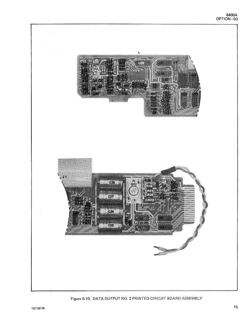
Figure 6-10. DATA OUTPUT NO. 2 PRINTED CIRCUIT BOARD ASSEMBLY
10/18/74
8400A OPTION-03
15
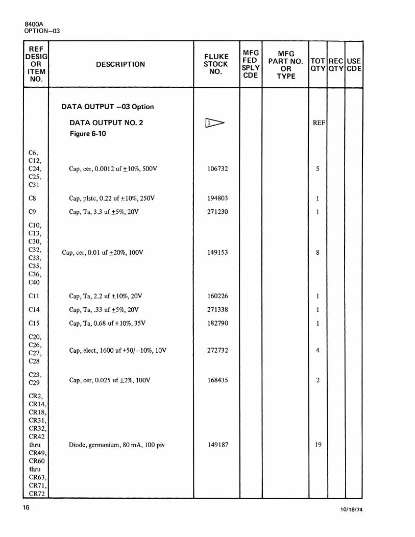
8400A OPTION-03
REF DESIG
OR ITEM NO.
C6, C12, C24, C25, C31
C8
C9
ClO, C13, C30, C32, C33, C35, C36, C40
Cll
C14
C15
C20, C26, C27, C28
C23, C29
CR2, CR14, CR18, CR31, CR32, CR42 th.ru CR49, CR60 th.ru CR63, CR71, CR72
16
DESCRIPTION
DAT A OUTPUT -03 Option
DATA OUTPUT NO. 2
Figure 6-10
Cap, cer, 0.0012 uf ±10%, 500V
Cap, plstc, 0.22 uf ±10%, 250V
Cap, Ta, 3.3 uf ±5%, 20V
Cap, cer, 0.01 uf ±20%, lOOV
Cap, Ta, 2.2 uf ±10%, 20V
Cap, Ta, .33 uf ±5%, 20V
Cap, Ta, 0.68 uf ±10%, 35V
Cap, elect, 1600 uf +50/-10%, lOV
Cap, cer, 0.025 uf ±2%, lOOV
Diode, germanium, 80 mA, 100 piv
MFG MFG FLUKE STOCK FED PART NO. TOT REC USE
NO. SPLY OR QTY QTY COE COE TYPE
[t:> REF
106732 5
194803 1
271230 1
149153 8
160226 1
271338 1
182790 1
272732 4
168435 2
149187 19
10/18/74

REF DESIG
OR DESCRIPTION ITEM NO.
CR3, CRIS, CR16, CR17, CR24 thru CR30, Diode, silicon, 150 mA CR35, CR57, CR64, CR66, CR69, CR70, CRIOq
CR19 thru Diode, silicon, 1 amp, 100 piv CR22
CR23 Diode, zener, 3 .9V, 20 mA
CR23 Diode zener, 4.3V
11 Connector, PCB to cable, 34 contact
QI, Q2, Q6, Tstr, silicon, NPN Q7, Q8
Q3, Q9, Tstr, silicon, PNP QB
Q4 Tstr, semicon, silicon NPN
QS Tstr, silicon, PNP Order by model and option no. (8400A 03 option)
QlO Tstr, silicon, NPN
Qll Tstr, silicon, NPN
Q12 Tstr, silicon, NPN
R4, RS, R30,
Res, comp, 4.7k ±5%, Y<iw R31, R61, R62,
10/18/74
MFG MFG FLUKE STOCK FED PART NO.
NO. SPLY OR COE TYPE
203323
116111
113316
180455
295337
218396
195974
218081
229898
168708
150359
288381
148072
TOT QTY
18
4
1
1
1
5
3
1
1
1
1
1
8
8400A OPTION-03
REC USE QTY COE
L
17

8400A OPTION-03
REF DESIG
OR ITEM NO.
R63, R64,
R14, R15
Rl6
R17
Rl8, R59
R19, R20, R21, R25, R26, R27
R22
R24, R55
R28
R29
R32
R33
R34
R35
R36
R37
R38
R39
R42
R45, R47, R53, R56
R46
18
DESCRIPTION
Res, comp, 2.7k ±5%, %w
Res, comp, 47k ±5%, %w
Res, comp, 6.8k±5%, %w
Res, comp, 680 ±5%, %w
Res, comp, lOk ±5%, %w
Res, fxd, met flm, l.62k ±1 %, 1/8w
Res, comp, lk ±5%, %w
Res, comp, 220 ±5%, %w
Res, comp, 1.8k ±5%, %w
Res, comp, 2.2k ±5%, %w
Res, comp, 3.3k ±5%, %w
Res, comp, 27k ±5%, %w
Res, comp, 15k ±5%, %w
Res, comp, 3.9k ±5%, %w
Res, comp, 5 .6k ±5%, %w
Res, var, cer met, 500 ± 10%, 1 w
Res, met flm, 182 ±1 %, 1/8w
Res, comp, 150k ±5%, %w
Res, fxd, met flm, 105k ±1 %, 1/8w
Res, met flm, 20.5k ±1%, %w
MFG MFG FLUKE STOCK FED PART NO. TOT REC USE
NO. SPLY OR QTY QTY COE COE TYPE
170720 2
148163 1
148098 1
148007 2
148106 6
283697 1
148023 2
147959 1
175042 1
148049 1
148056 1
148114 1
148148 1
148064 1
148080 1
291120 1
20020 1
182212 1
291294 4
261669 1
10/18/74
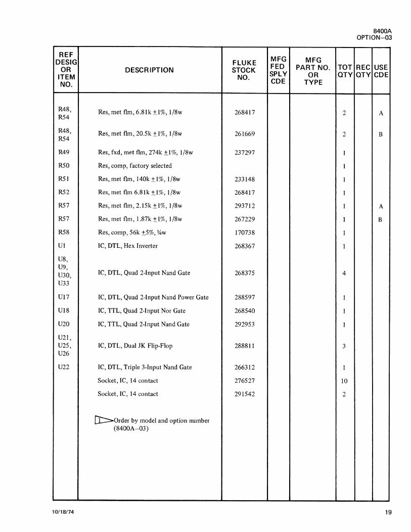
REF DESIG FLUKE
OR DESCRIPTION STOCK ITEM NO. NO.
R48, Res, met flrn, 6.8lk ±-1%, 1/8w 268417 R54
R48, Res, met flrn, 20.Sk ±1%, 1/8w 261669 R54
R49 Res, fxd, met flm, 274k ±1 %, 1/8w 237297
R50 Res, comp, factory selected
R51 Res, met flrn, 140k ±1%, 1/8w 233148
R52 Res, met flrn 6.81k ±1%, l/8w 268417
R57 Res, met flm, 2.15k ±1%, 1/8w 293712
R57 Res, met flm, 1.87k ±1%, 1/8w 267229
R58 Res, comp, 56k ±5%, ¥.iw 170738
U1 IC, DTL, Hex Inverter 268367
U8, U9,
IC, DTL, Quad 2-Input Nand Gate 268375 U30, U33
U17 IC, DTL, Quad 2-Input Nand Power Gate 288597
Ul8 IC, TTL, Quad 2-Input Nor Gate 268540
U20 IC, TTL, Quad 2-Input Nand Gate 292953
U21, U25, IC, DTL, Dual JK Flip-Flop 288811 U26
U22 IC, DTL, Triple 3-Input Nand Gate 266312
Socket, IC, 14 contact 276527
Socket, IC, 14 contact 291542
[):::::>order by model and option number (8400A-03)
10/18/74
MFG MFG FED PART NO. TOT SPLY OR QTY CDE TYPE
2
2
I
1
1
1
1
1
1
1
4
1
1
1
3
1
10
2
8400A OPTION-03
REC USE QTY CDE
A
B
A
B
19
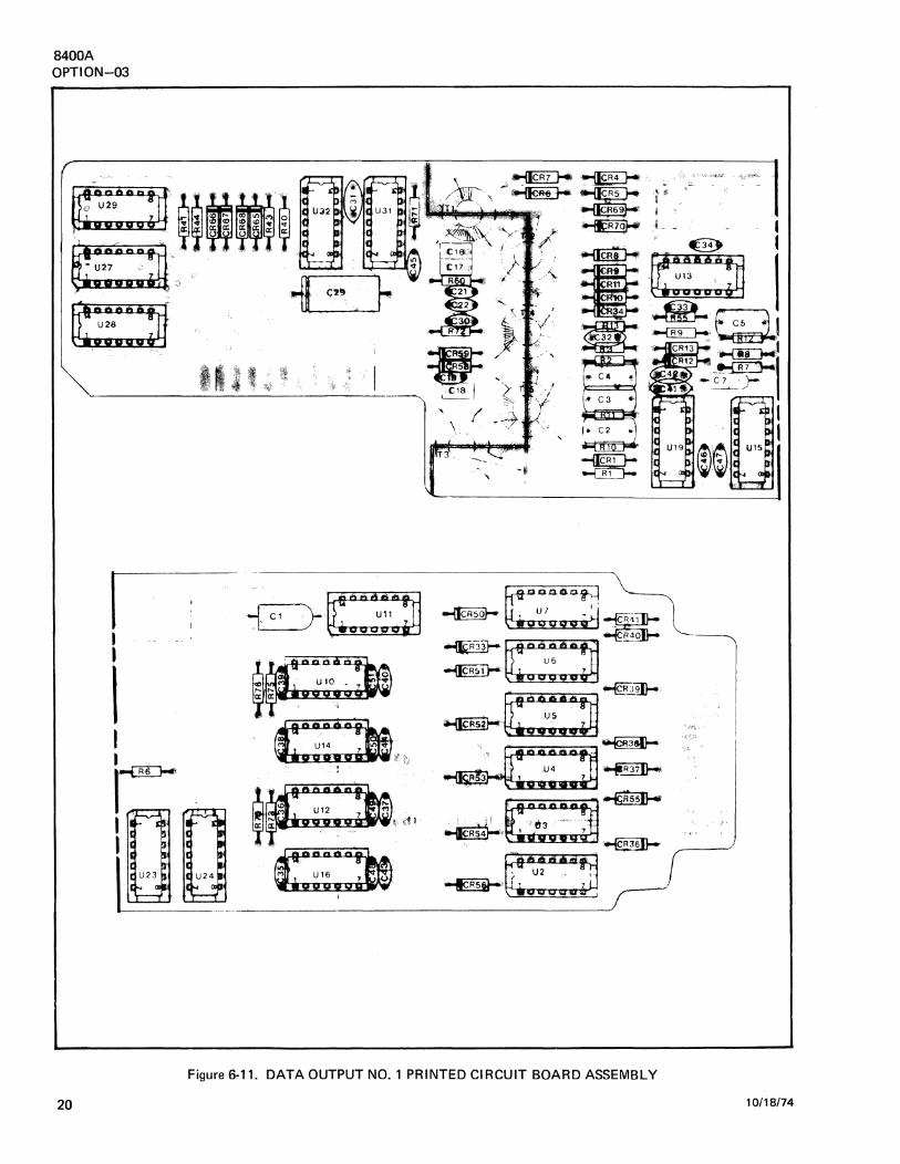
8400A OPTION-03
~;;·::::g . Iii,#~
. "
Figure 6-11. DATA OUTPUT NO. 1 PRINTED CIRCUIT BOARD ASSEMBLY
20 10/18/74
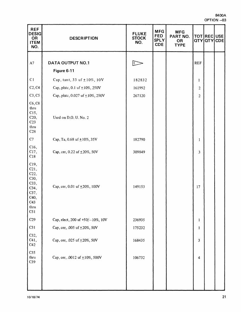
REF DESIG
OR DESCRIPTION ITEM NO.
A7 DATA OUTPUT N0.1
Figure 6-11
CI Cap, tant, 33 uf ±10%, IOY
C2,C4 Cap, piste, 0.1 uf ±10%, 2SOY
C3,CS Cap, piste, 0.027 uf ±10%, 2SOY
C6,C8 thru CIS, C20, Used on D.O. U. No. 2 C23 thru C28
C7 Cap, Ta, 0.68 uf ±10%, 3SY
CI6, CI7, Cap, cer, 0.22 uf ±20%, SOY CI8
CI9, C21, C22, C30, C33,
Cap, cer, 0.01 uf ±20%, lOOY C34, C37, C40, C43 thru CSI
C29 Cap, elect, 200 uf +S0/-10%, lOY
C31 Cap, cer, .OOS uf±20%, SOY
C32, C41, Cap, cer, .02S uf ±20%, SOY C42
C3S thru Cap, cer, .0012 uf ±10%, SOOY C39
10/18/74
MFG MFG FLUKE STOCK FED PART NO.
NO. SPLY OR COE TYPE
[::::>
182832
161992
267120
182790
309849
1491S3
23693S
l 7S232
16843S
106732
TOT QTY
REF
I
2
2
I
3
17
I
I
3
4
8400A OPTION -03
REC USE QTY COE
21

8400A OPTION -03
REF DESIG
OR ITEM NO.
CRl, CR4 thru CR13, CR33, CR34, CR36 thru CR41, CR50 thru CR56, CR58, CR59, CR65 thru CR70
CR2, CR3, CR14 thru CR32, CR35, CR42 thru CR49, CR57, CR60 thru CR64
P22
Rl, Rl l
R2,R3 R72
R4,R5 R14 thru R39, R45 thru R54
R6,R7 Rl3
22
DESCRIPTION
Diode, germanium, 80 mA, 100 piv
Not Used
Connector, PCB to cable, 34 contact
Res, comp, 100 ±_5%, %w
Res, comp, 220 ±_5%, %w
Not Used
Res, comp, 3.9k ±_5%, %w
FLUKE MFG MFG
STOCK FED PART NO. TOT REC USE
NO. SPLY OR QTY QTY CDE CDE TYPE
149187 34
295337 1
147926 2
147959 3
148064 3
10/18/74

REF DESIG
OR DESCRIPTION ITEM NO.
R8, R40, R41, Res, comp, 4 70 ±5%, %w R43, R44
R9, Res, comp, 12k ±5%, %w RSS
RIO Res, comp, lOk ±5%, %w
R12 Res, comp, lk ±5%, Y<iw
R60, Res, comp, 390 ±5%, %w R71
R73 thru Res, comp, 27 ±5%, %w R76
Tl thru Transformer, pulse TS
Ul, U8, U9, U17, U18, U20, Not Used U21, U22, U25, U26, UJO
U2 thru U7, Ull, U24, IC, DTL, Quad 2-Input Nand Gate U27, U28, U29
UlO, U12,
IC, TTL, 8-Bit Shift Register U14, U16
10/18/74
MFG FLUKE MFG STOCK FED PART NO.
NO. SPLY OR CDE TYPE
147983
159731
148106
148023
147075
160812
275362
268375
272138
TOT QTY
5
2
1
1
2
4
5
11
4
8400A OPTION -03
REC USE QTY CDE
23

8400A OPTION -03
REF DESIG
OR ITEM NO.
Ul3, U32
UIS, U19
U23
U31
DESCRIPTION
IC, DTL, Hex Inverter
IC, TTL, Quad 2-Input Nor Gate
IC, DTL, triple 3-Input Nand Gate
IC, TTL, Hex Inverter
Socket, IC, 14 contact
Socket, IC, 14 contact Low profile
[I:::> Order by model and option no. (8400A-03 option)
6-49. SERIAL NUMBER EFFECTIVITY
6-50. A Use Code column is provided to identify certain parts that have been added, deleted, or modified during production of the Model 8400A. Each part in this option for which a use code has been assigned may be identified with a particular printed circuit board serial number by consulting the Use Code Effectivity List below. All parts with no code are used on all printed circuit boards with
24
MFG MFG FLUKE FED PART NO. TOT REC USE STOCK SPLY OR QTY QTY COE NO. COE TYPE
268367 2
268540 2
266312 1
292979 1
276527 17
291542 4
serial numbers 123 and on. NOTE: These Use Codes and Serial Number Effectivity apply to this option printed circuit board assembly only. For the standard instrument configuration, see Section 5, paragraph 5-9, and for additional options, see the appropriate option subsection.
USE CODE
A B
SERIAL NUMBER EFFECTIVI1Y
Serial number 123 through 148. Serial number 149 and on.
10/18/74
6-1. INTRODUCTION
6-2. The AS Remote Control Unit (Option-04) enables the Model 8400A to be programmed remotely. The RCU provides the capability of controlling all functions and ranges, with logic interlocking provided to make it impossible to call two or more incompatible functions simultan
eously.
6-3. SPECIFICATIONS
6-4. Specifications for the Remote Control Unit are
located in Section 1 of the manual.
6-5. INSTALLATION
6-6. The following procedure is to be used to install the Remote Control Unit in the Model 8400A (refer to Section S, Figure S-1).
a. Disconnect the power cord from the instrument.
b. Remove the top dust and guard chassis covers.
c. Determine that connector JS, on the Al4 Display board, is clear of obstructions and that alignment spacers are inserted between pin pairs J S-1, -2; JS-3, -4 and JS-7, -8; JS-9, -10.
d.
e.
Determine that connector slot on rear panel for Pl 9 on Remote Control Unit board is clear of any obstructions.
Attach spring to bottom portion of guard bar.
8400A OPTION -04
Option-04
Remote Control Unit
f.
g.
h.
i.
Insert Pl 9 into connector slot on rear panel (refer to Section S, Figure S-1 ).
Insert edge of Remote Control Unit board into card guide on the inner chassis bulkhead.
Observe that alignment spacers on JS line up with slots on the Remote Control Unit card-edge connector.
Slide pcb downward until the card-edge connector is fully engaged with JS on Al4 Display board.
j. Attach top guard and chassis covers, connect ac power, and perform receiving inspection test of the Remote Control Unit as described in paragraph 6-27, Performance Test.
6-7.
6-8.
OPERATING INSTRUCTIONS
Operation of the DVM with the AS Remote Control Unit installed is covered in Section 2.
6-9. THEORY OF OPERATION
6-10. General
6-11. The RCU functional block diagram is given in Figure 6-1. The input function and range commands are applied to coders and then delivered to a multiplexer. The multiplexer receives sequential address information from a counter and, combined with the range and function codes,
applies control information to two isolation pulse transformers. The serial output of these two pulse transformers

8400A OPTION -04
is applied to the shift register for conversion back to 8 time slots which is then buffered and decoded and presented for
use. For the following discussion refer to Schematic Diagram 8400A-1011, Figure 6-1 and Figure 6-2.
2
1000
RANGE
CODER
0
" < ~ ~
I I I
I
~"l"•l!\~·1"• I
RANGE CODES
G
FCT. CODES
t--N~t---i--~;''°~ ··-· -KSJ - -
+---+---+-- --11- . -~-~-------------- -
EXT.REF.---~~~....,
FILTER ------
FUNCTION
CODER
M:~:',::ILER "0"> 1:1[ ~:2·0"•
~K~----t:>- EXT. REF. CONT. LN. T2
'"-"-------£>--FILTER CONT. LN.
TRIG. INPUT ------- ~~7~~~~ & RESET
SAMPLE COUNTER
FUNCTION
DECODER
GATE -------OSCILLATOR
2KHZ '-"'G----.1 RANGE
H DECODER
GATED OSCILLATOR 500 KHZ
GATE
Figure 6-1. 8400A REMOTE CONTROL UNIT BLOCK DIAGRAM
SAMPLE TRIGGER ------,,--------------------------
lJ2·PINS
500 KHZ CLOCK U1-PIN 13
2 BIT
PIN 11------------'
U2 4 BIT
PIN 9 ----------------~
8 BIT PIN6 _____ ~
--o---l--s-+-9---!--10-i--11+12-+-13---!--1•-+-1;-.+--o-~ L E;T J HG F
FUNCl !ON REF AUTO
MULTIPLEXER U3PIN15
TRANSFORMER GATES "l"S Ul PIN l
EMITTER Q3
EMITTER Q4
SHIFT REG. CLOCK ----i,-----ir-UB-P!N 1 u I
LATCH CLOCK EMITTER QS
v
v r
Figure 6-2. REMOTE CONTROL SAMPLE LOAD SEQUENCE
voe } FUNCTION VAC CONTROL
Kf.! LINES SJ
Ro
s, } """"' "" COUNTER Sb CONTROLS "R, s,
6-12. Circuit Description
6-13. FUNCTION AND RANGE CODERS. The purpose of the function and range coders is to compress the 12 input lines into 8 channels with function/range interlocking. Transistor Ql S, inverters Ul S A, C, F and diodes CR2, 3, 4, S, 12, 19 and 20 combined are the function/range interlocking feature which disallows incorrect function and range combinations. Gates USA, USB, U6A through U6D present encoded range and function information to the digital multiplexer. Table 6-1 shows Function codes and Table 6-2 shows Range codes.
INPUTS VAC
1 0 1 1
Kn
1 1 0 1
8400A OPTION -04
Table 6-1. FUNCTION CODES
RESULTING INFORMATION COMMAND CHANNEL
n N R
1 VDC 0 0 1 VAC 0 1 1 Kn 1 0 0 n 1 1
Table 6-2. RANGE CODES
FUNCTION COMMANDS RANGE POSSIBLE INFORMATION WITH THESE RCUINPUTS CHANNEL OUTPUTS RESULTING RANGES 10k 1k 100 10 1 0.1 F G
n,Kn,AC,DC 1 1 1 1 1 1 1 1 n,Kn 0 1 1 1 1 1 0 0 n, Kn, AC, DC 1 0 1 1 1 1 0 0 n, Kn, AC, DC 1 1 0 1 1 1 0 1 n,AC,DC 1 1 1 0 1 1 0 1 AC,DC 1 1 1 1 0 1 1 0 DC ONLY 1 1 1 1 1 0 1 0
6-14. COUNTER AND GATED OSCILLATOR. The purpose of the counter and gated oscillator circuitry is to supply sequential address information to the multiplexer in response to the 8 bit set pulses from the Schmitt Trigger and Sample Oscillator Circuitry. The 8 bit set pulses reset the counter to an 8 state (i.e. 1000). The counter U2 then releases the gated oscillator and allows it to oscillate at SOO kHz. Gates UIC and UID, capacitors Cl, C2 and resistors RI, R2 are the gated SOO kHz oscillator circuitry. The output of the gated oscillator is applied to the counter U2. When enabled, the oscillator causes the counter to cycle through eight states. (Refer to Table 6-3). As soon as state "O" (i.e. 000) is reached by the counter, the oscillator is disabled by the counter, which in turn stops the counter from further counting. This sequence will not start again until an 8 bit set pulse is received by the counter from the Schmitt Trigger circuitry.
6-IS. SCHMITT TRIGGER AND SAMPLE OSCILLATOR. The purpose of the Schmitt Trigger and Sample Oscillator is to set the sample rate of the RCU. Gates U4A through U4D, capacitors C3 and C4, resistors R3, R4, RS and diodes CR30 and CR31 comprise the Schmitt Trigger and Sample Oscillator circuitry. There are two possible
H J
1 0 0 1 1 1 0 1 1 1 0 1 1 1
Ra Sa Rb Sb Re Sc RANGE
1 1 1 1 1 1 AUTO 0 1 0 1 0 1 10k 0 1 0 1 1 0 1k 0 1 1 0 0 1 100 0 1 1 0 1 0 10 1 0 0 1 0 1 1 1 0 0 1 1 0 0.1
modes of operation for this circuitry: continuous or triggered command mode.
6-16. CONTINUOUS COMMAND MODE. In this mode of operation, Pl 9-33 (EXTERNAL COMMAND ENTRY) and P19-3S (AUTO COMMAND DEFEAT) must be at logic level "l" (+SV de or open). A "1" command simultaneously present at pin 1 of gate U4A and pin S of gate U4B will cause gates U4A, B, C and D to oscillate. The frequency of
Table 6-3. COUNTER SEQUENCE
STATE COMMENTS
0000 Oscillator is enabled at this point and count 1000 sequence begins. 1001 1011 1010 1100 1101 1110 1111 0000 Oscillator is disabled at this point.
3

8400A OPTION -04
the oscillation is 2kHz as determined by R3, C4. Each pulse in the 2kHz pulse train at pin 8 of U4C acts as the 8 bit set pulse for counter U2. Thus, commands are updated at a 2kHz rate. Since this rate is faster than the instrument can respond, command appears continuous.
6-17. TRIGGERED COMMAND MODE. In this mode of operation, P19-35 (AUTO COMMAND DEFEAT) is held at logic level "O" and an external trigger is applied to P19-33 (EXTERNAL COMMAND ENTRY). With a logic level "O" at P19-35 gate U4A is disabled. The application of an external pulse to P19-33 will enable the schmitt trigger circuit, gates U4B, C and D, resulting in a negative pulse presented to the counter. As in the continuous command mode, this pulse initiates the command update cycle.
6-18. DIGITAL MULTIPLEXER. The Digital Multiplexer U3 is a medium scale integrated circuit constructed to connect various input signals, one at a time, to a single two-phase output in response to certain input addresses. Table 6-4 defines its operation. The output is serialized into eight time slots; each is lµs in length.
6-19. PULSE TRANSFORMER CIRCUITRY. The purpose of this circuitry is to couple the serialized information to the shift register and provide isolation. Gates UlA and Ul B pass the serialized information to primaries of pulse transformers Tl and T2 through buffer Ql, Q2, Gate UlA passes logic "l" information, and gate Ul B passes Logic "O" information. The secondaries of Tl and T2 impose their respective logic to buffers Q4 and QS and thereby to the shift register.
6-20. 8 BIT SHIFT REGISTER MEMORY. J-K flip flops U7A & B, U8A & B, U9A & Band UlOA & B com-
prise the shift register. Diodes CRl 0, CRl l, resistors R23, R24 comprise the clock network for the flip flops. The loading of the shift register occurs at pins 2 and 3 of U7 A. The logic sequencially shifts through the flip flops until the last pulse of the loading cycle is loaded into U7 A. At this time the shift register is fully loaded and will not change until another loading cycle occurs.
6-21. 8 BIT LATCH BUFFER MEMORY. Ul l and latch clock network, transistor QS, diodes CR6 and CR7 plus capacitor CS, comprise the 8 Bit Latch Buffer Memory circuit. During the loading cycle of the 8 bit shift register memory circuit, transistor QS is turned on, which disconnects the inputs of ICUl 1 to preclude undesirable pulsing of output lines during the loading cycle. After the shift register is fully loaded, transistor QS turns off, thereby allowing the outputs of Ul 1 to assume the states of the present inputs.
6-22. DECODERS. Decoder-buffers Ul2, U13, U14 and transistors Q6-Ql 1 decode the Ul l latch information to the same format as seen on the inputs. Diodes CR21, CR22 provide for external reference lockout in Ohms and Kil functions as is done by the front panel pushbuttons when the instrument is commanded locally.
6-23. MAINTENANCE
6-24. Introduction
6-25. This section contains maintenance information for the Remote Control Unit. Factory service information and general instructions regarding instrument access and cleaning are located in Section 4 of the manual.
Table 6-4. MULTIPLEXER OPERATION
THEN OUTPUT AND OUTPUT CHANNEL IF THE INPUT PIN 15 HAS PIN 14 HAS INFORMATION ADDRESS IS: THE SIGNIFICANCE THE SIGNIFICANCE IS:
PIN PIN PIN 13 12 11
-0 0 0 R (pin 1) R FUNCTION BIT 0 0 1 N (pin 2) N FUNCTION BIT 0 1 0 L (pin 3) L FILTER 0 1 1 K (pin 4) i< ICXTERNAL REFERENCE 1 0 0 J (pin 5) J AUTO RANGE -1 0 1 H (pin 6) H RANGE LSB 1 1 0 G (pin 7) G RANGE BIT 1 1 1 F (pin 9) F RANGE MSB
4
6-26. Performance Test
6-27. The following performance test exercises each RCU input to determine if the unit is working properly. The performance test should be conducted before any instrument maintenance is attempted. The test should be conducted under the following environmental conditions: Ambient Temperature 0°C to 50°C, Relative Humidity less than 70%. An instrument that fails the performance test will require corrective maintenance. In case of difficulty, analysis of the test results, with reference to the troubleshooting section, should help to locate the trouble.
6-28. To test the RCU, proceed as follows:
a. Supply +5 volts de to the RCU, P19-9 (+5V de) and
b.
c.
COMMANDED FUNCTIONS
FUNCTIONS RANGES DC AC Kil
Fl LT, EXT REF* .1 0 0
0 0 10 0 0 100 0 0 1000 0 0 NONE 0 0
FIL T, EXT REF,* U* 10 0
100 0 1000 0 10K 0
FIL T, EXT REF,* Kil 100 0 1000 0
10K 0 NONE 0
P19-2 or 4 or 6 (common).
8400A OPTION -04
Press REMOTE FUNCTION switch on the Model 8400A front panel.
Activate each of the combination of functions and ranges shown in column 1 and 2 of Figure 6-3 by contact closure between the appropriate pin and common of the RCU connector (refer to Table 2-5 of Section 2 for connector pin assignments). Observe the resulting front panel display and verify correct response for each call combination listed in Figure 6-3. Function annunciator will not show option functions if the pertinent option is not installed.
DVM RESPONSE
RANGES
x REF FILTOVER .1 1 10 100 1000 10K
0
0 0
0 0 0
0
0 0
0 0
0
0
0 0
0 0
0 Down ranges from 1000 to .1
0
0 0
0
0 0
0 Autoranges in the following order: 1 O,OOOK, 1 OOOK, 1 OOK, 10il and STOP
EXT* REF, VAC* 1--~~1~~~----+-~o'--·t-~+-=o-+~-+~~~~~-4--~-+-~o=--+-~+-~+--~+-~-1 10 0 0 0
i--~~~-J.-~--;~-r~--+~-t~~~~~~~-+-~-1-~-+-~-l-~-+.~--1-~---1
-1--~~1~00"--+----+--o~t--~+-o~+-~1--~-1--~-~~-+-~-+-~-+-~o;......+~--1~___. 1000 0 0 0
1--~~~-+·-·--+~-t-~--+~--+~--1-~--1~~-f-~-'-~-'-~--'-~--'-~--'-~~•
NONE 0 0 Downranges from 1000 to 1
*Options Disregard DVM response for these functions if option is not installed.
Figure 6-3. REMOTE CONTROL UNIT TEST REQUIREMENTS
5

8400A OPTION -04
6-29. Calibration
6-30. The RCU does not require calibration.
6-31. Troubleshooting
6-32. This section contains information designed to aid in troubleshooting the RCU. Before attempting to troubleshoot the RCU, however, it should be verified that the
trouble is actually in the instrument and is not caused by faulty external equipments or improper control settings. For this reason, the performance test (paragraph 6-26) is suggested as a first step in troubleshooting. The performance test may also help to localize the trouble to a particular section of the instrument. If the performance test fails to localize the trouble, the trouble analysis flow chart in Figure 6-4 and code information in Figure 6-5 may be helpful.
START
6
YES >-------- STOP
NO CONNECTPOWERTORCU >----I~ THROUGH PJ9-9 (+5V DC) .,_ _ __,_,
YES
AND PJ9·4 (COMMON)
CHECK DECODER CIRCUITRY
CHECK LATCH CLOCK AND IC Ull
CHECK PULSE TRANSFORMER CIRCUITRY
CHECK 500 kHz GATED OSCILLATOR, COUNTER, SCHMITT TRIGGER
CHECK CODER CIRCUITRY
Figure 6-4. REMOTE CONTROL UNIT TROUBLE ANALYSIS (FLOW CHART)

RANGE CODES
F G HJ RANGE 0 AUTO
0 0 0 1 10,000 0 0 1 1 1000 0 1 0 1 100 0 1 1 1 10 1 0 0 1 1 1 0 1 1 0.1
FCT. CODES
N R FUNCTION 0 0 VDC 0 1 VAC 1 0 Kn 1 1 n
8400A OPTION -04
Figure 6-5. FUNCTION AND RANGE CODES
6-33. LIST OF REPLACEABLE PARTS
6-34. For column entry explanations, part ordering information and basic instrument configuration Use Codes
and Serial Number Effectivity List, see Section 5, para
graphs 5-1 through 5-10. See paragraph 6-35, this option subsection, for additional Use Codes and Serial Number
Effectivity List assigned to this printed circuit assembly
option.
6-35. SERIAL NUMBER EFFECTIVITY
6-36. A Use Code column is provided to identify certain parts that have been added, deleted, or modified during
10/18/74
production of the Model 8400A. Each part in this option for which a use code has been assigned may be identified with a particular printed circuit board serial number by consulting the Use Code Effectivity List below. All parts with no code are used on all printed circuit boards with serial numbers 123 and on. NOTE: These Use Codes and Serial Number Effectivity apply to this option printed circuit board only. For the standard instrument configuration,
see Section 5, paragraph 5-9, and for additional options,
see the appropriate option subsection.
USE CODE
A
B
SERIAL NUMBER EFFECTIV11Y
Serial number 123 through 313
Serial number 314 and on
7

8400A OPTION -04
REF DESIG
OR ITEM NO.
DESCRIPTION
AS REMOTE CONTROL -04 Option
Figure 6-6
Cl,C2 Cap, mica, 1 SOO pf ±S%, SOOV
C3 Cap, mylar, .01 uf ±20%, lOOV
C3,C6 Cap, cer, 1200 pf ±10%, SOOV
C6, Cap, cer, 1200 pf ±10%, SOOV ClS
C4 Cap, Ta, 0.68 uf ±10%, 3SV
C4 Cap, Ta, 3.3 uf ±10%, 3SV
cs Cap, Ta, 1 uf ±20%, 3SV
C7 Cap, elect, 200 uf +S0/-10%, 1-V
C8 Cap, cer, 0.01 uf+80/-20%, SOOV
(Deleted)
C9 Cap, mica, 33pf ±S%, SOOV
ClO, Cap, cer, .02S uf ±20%, SOV Cl 1
C12, Cap, cer, .OOS uf ±20%, SOV C13
C14 Cap, Tan, 39 uf ±20%, 20V
CRl thru CR12,
Diode, germanium, 80 mA, 100 piv CR19 thru CR28
CR13 thru CR18,
Diode, silicon, 1 SO mA CR29 thru CR36
CR13 thru CR18, CR29 Diode, silicon, lSO mA thru CR32, CR36
8
MFG MFG FLUKE STOCK FED PART NO. TOT REC USE
NO. SPLY OR QTY QTY COE COE TYPE
REF
148361 2
1497S3 1 B
106732 2 A
106732 2 B
182790 1 A
182808 1 B
161919 1
23693S 1
10S668 1 A
B
160317 1 B
16843S 2 B
17S232 2 B
16391S 1 B
149187 22
203323 14 A
203323 11 B
10/18/74
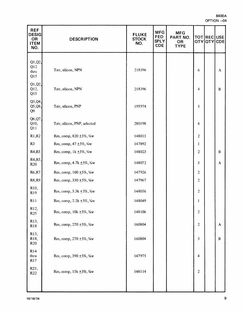
REF DESIG
OR DESCRIPTION ITEM NO.
Ql,Q2 Q12 thru Tstr, silicon, NPN
Q15
Ql,Q2 Q12, Tstr, silicon, NPN Q15
Q3,Q4 Q5,Q8, Tstr, silicon, PNP Q9
Q6,Q7, QlO, Tstr, silicon, PNP, selected Ql l
Rl,R2 Res, comp, 820 ±5%, %w
R3 Res, comp, 47 ±5%, %w
R4,R5 Res, comp, lk ±5%, %w
R4,R5, Res, comp, 4.7k ±5%, %w R20
R6,R7 Res, comp, 100 ±5%, %w
R8,R9 Res, comp, 330 ±5%, %w
RIO, Res, comp, 3.3k ±5%, %w R19
Rll Res, comp, 2.2k ±5%, %w
R12, Res, comp, lOk ±5%, %w R25
R13, Res, comp, 270 ±5%, %w R18
Rl3, R18, Res, comp, 270 ±5%, %w R20
R14 thru Res, comp, 390 ±5%, %w R17
R21, Res, comp, 15k ±5%, %w R22
10/18/74
MFG MFG FLUKE STOCK FED PART NO.
NO. SPLY OR COE TYPE
218396
218396
195974
280198
148015
147892
148023
148072
147926
147967
148056
148049
148106
160804
160804
147975
148114
TOT QTY
6
4
5
4
2
1
2
3
2
2
2
1
2
2
3
4
2
8400A OPTION -04
REC USE QTY COE
A
B
B
A
A
B
9

8400A OPTION -04
REF DESIG
OR ITEM NO.
R23, R24
R26, R27
Tl,T2
Ul
U2
U3
U4
U4,U61 U12, U13, U14
us
U6, U12, U13, U14
U7
U8,U9 UlO
Ul 1
UIS
10
DESCRIPTION
Res, comp, l .2k ±_S%, ~w
Res, comp, 4.7k ±_S%, ~w
Transformer, pulse
IC, TTL, Quad 2-Input Nor Gate
IC, DTL, Binary Counter
IC, TTL, Digital Multiplexer
IC, TTL, Quad 2-Input Nand Gate
IC, DTL, Quad 2-Input Nand Gate
IC, DTL, dual 4-Input Nand
IC, DTL, Quad 2-Input Nand Gate
IC, TTL, dual J-K Flip-Flop
IC, DTL, dual J-K Flip-Flop
IC, TTL, 8-Bit Latch
IC, DTL, Hex Inverter
Socket, IC, 14 contact, Ul, U2, U4, US, U6, U8, U9, UlO & Ul2 thru UIS
Socket, IC, 16 contact, U3 & U7
Socket, IC, 24 contact, Ul 1
MFG MFG FLUKE FED PART NO. TOT REC USE STOCK NO. SPLY OR QTY QTY CDE
CDE TYPE
190371 2
148072 2 B
27S362 2
28884S 1
2671S3 1
2888S2 1
2929S3 1 B
26837S s A
268383 1
26837S 4 B
268441 1
288803 3
288837 1
268367 1
276S27 12
276S3S 2
292946 1
10/18/74

10/18/74
CR14~ CR13") )
Figure 6-6. REMOTE CONTROL UNIT PCB ASSEMBLY
8400A OPTION - 04
11


8400A OPTION-05
Option-05
DC External Reference
6-1. INTRODUCTION
6-2. The OC External Reference {Option -05) enables the user to substitute an external voltage for the internal reference of the Model 8400A. The principal use of the DVM when operated in this matter is for four-wire voltage ratio measurements: ±de to de, and ac to de.
6-3. SPECIFICATIONS
6-4. Specifications for the OC External Reference are located in Section 1 of the manual.
6-5. INSTALLATION
6-6. The following procedure should be used to install the OC External Reference option in the Model 8400A.
NOTE
The DC External Reference option is not field installable in 8400A mainframes serial No. 634 and below.
a. Disconnect power cord from line power.
b.
c.
d.
10/18/74
Remove the Model 8400A top dust cover and top inner guard chassis cover.
Determine that connector J3 on A14 Display board is clear of obstructions and that alignment keys are inserted between pin pairs B-1, -2; 13-3, -4and13-13, -14; B-15, -16.
Remove connector mounting bracket located on rear portion of inner chassis, next to power transformer.
e. Mount the OC External Reference connector to the connector bracket with orientation as shown on the rear panel decal. The lug attached to pin 1 of the connector is to be attached to the guard chassis through one of the mounting screws on the OC External Reference connector.
f. Reinstall connector mounting bracket on the inner chassis.
g.
h.
i.
Align OC External Reference board with vertical card guides mounted on inner chassis bulkhead.
Align rubber grommet with slot in rear inner chassis and slide grommet into slot.
Slide OC External Reference board downward while observing that alignment keys on J3 are in proper alignment with the slots in the printed circuit board.
j. Engage printed circuit board fully in J3 connector.
k.
6-7.
Attach guard and top dust covers, connect power cord to line power, and perform receiving inspection test of OC External Reference assembly as described in paragraph 6-26, Performance Test.
OPERATING INSTRUCTIONS
6-8. Operating instructions for the Model 8400A with OC External Reference installed are located in Section 2 of the manual.

8400A OPTION-05
6-9. THEORY OF OPERATING
6-10. General
6-11. The OC External Reference unit consists basically of an input divider, an isolation circuit, and a buffer amplifier, as shown in Figure 6-1.
HIGH
7o10 DIVIDER
REFERENCE COMMON
Figure 6-1. DC EXTERNAL REFERENCE SIMPLIFIED DIAGRAM.
REF
OUT
The input divider produces an output that is 7/10 of the reference input voltage. The circuit is designed to operate with a reference input voltage between + 1 and + 10.S volts de. The isolation circuit provides a means of isolating the input common of the OC External Reference unit from the output common of the OC External Reference unit. This is necessary to provide 4 terminal ratio capability, and because the Model 8400A input common terminal (LO) and the instrument common are not equivalent. In fact, the LO instrument INPUT terminal is the actual input to the
A/D Converter and can have a potential of ± 12 volts de with respect to instrument common. Switches Sl and S2 are arranged so that when one is closed, the other is open. Sl is closed during a non-critical portion of the measurement cycle (A/D zero time) and capacitor C is allowed to charge to voltage ER" When S2 is closed, the output of A1 must be ER.
6-12. Circuit Description
6-13. INPUT DIVIDER. The input divider consists of resistors R3 through RS. The input divider is adjusted by resistor R4, {lOV CAL control). Capacitor Cl together with the divider resistors form an RC filter which improves the signal to noise ratio.
6-14. ISOLATION CIRCUIT. Input dual MOSFET Q9 functions as switch S 1 in the simplified diagram and JFET
2
switches Q4 and QS function as switch S2. Transistors Ql and Q2 are gate drivers for switches Q4 and QS. Using the reference voltage for the collector supply of Q2 assures that the gate signal of Q4 never goes positive with respect to its source and drain terminals. The gate of QS is clamped to within 0.2 volts of common by diode CR3. Resistor R11 limits the current through CR3 and capacitor C4 compensates for the capacity of CR3. 6-15. BUFFER AMPLIFIER. The buffer amplifier consists of super beta transistor Q8 followed by operational amplifier Ul. Transistor Q7 and resistor R23 comprise a constant current source for amplifier Q8. Resistor R29 provides base current for the input terminal of transistor Q8. Transistor Q6 and associated circuitry provide a constant current source for the collectors of Q8. Transistor Q8 is bootstrapped by the output of amplifier Ul, via resistors RlS and Rl6, to increase the SMRR of the buffer amplifier. Frequency compensation is provided by capacitors C7, C8. Capacitor C6 holds the input voltage to the buffer amplifier during the time switches Q4 and QS are off. The reference voltage in the A/D Converter is sensed through resistor R28, thereby compensating for line drops. Low sense {reference common) also originates in the Logic and A/D assemblies. Diodes CR8 and CR9 provide feedback to the voltage follower input when reed relay Kl is open, thereby maintaining amplifier output within 0.5 volts of the voltage on C2 and thus controlling the gate drive for Q4. Resistors R30 through R32, coupled with resistor R28, generate small corrections in the output reference voltage to compensate small errors proportional to the voltage difference between the input common and circuit common.
6-16. VOLTAGE DISTRIBUTION. Voltage distribution is shown in the simplified schematic Figure 6-2. Since Q9 is a P-channel enhancement mode device, a negative gate voltage of 2 volts or more is needed to ensure that the transistor is on. Zero volts or a positive gate voltage turns the transistor off. As shown in the figure, the upper switch needs a minimum of - 7 .2S volts to turn on and a maximum of ~20 volts to turn off under all possible operating circumstances.
6-17. The MOSFET gate driver is redrawn in Figure 6-3 to show the peak voltages. When Q3 is saturated, CR4 is back biased. When the transistor is cutoff, CS charges to
8 volts because of the 12 volt drop across the zener. This voltage subtracts from the collector voltage giving the vol
tage shown.
6-18. DISABLE AND PROTECTION CIRCUITS. When the external reference is called, relay Kl is energized by QlO and the internal reference disable line is pulled to +SV. Input protection is provided by diodes CRl and CR2 and fuse Fl.

+1 to +10.5 VOLTS INPUT
~---~~~~~I___. ._~l'--~-
1 I -5.25 19.95 : I ~ I Jog
o.1++7.35 I : I
c~~~~--411~--+~~_._~, ........ r~,~~~
Ot.12.6V ~ Figure 6-2. VOLTAGE DISTRIBUTION IN MOSFET 09.
+18V
-18V
-+18V 12V
, CR5
12V
1J -26V
Figure 6-3. GATE DRIVER VOLTAGES.
6-19. MAINTENANCE
6-20. Introduction
6-21. This section contains maintenance information for the DC External Reference. Factory service information and general instructions regarding instrument access and cleaning are located in Section 4 of the manual.
6-22. Fuse Replacement
6-23. There are two fuses located on the DC External Reference board. Fl is the active fuse and is to be replaced with the SP ARE FUSE when necessary. Both fuses are 15 ma, pigtail fuses.
8400A OPTION-05
6-24. Test Equipment
6-25. The following equipment is recommended for performance testing, troubleshooting, and calibration of the DC External Reference. If the recommended equipment is not available, equivalent or better instruments may be substituted.
EQUIPMENT RECOMMENDED NOMENCLATURE EQUIPMENT
DC Voltage Source Fluke Model 343A DC Voltage Calibrator
Kelvin Varley Divider Fluke Model 720A
Oscilloscope Tektronix Model 547
Oscilloscope Plug-IN Tektronix Model lAl
6-26. Performance Test
6-27. The performance test in this section compares the DC External Reference performance to the accuracy specifications in Section 1 of the manual to determine if the unit is in calibration. To test the unit, a reference voltage is applied to the DC External Reference input terminals, a de voltage is applied to the DVM INPUT terminals, and proper DVM readout is verified. The performance test should be conducted before any instrument maintenance or calibrating is attempted. The test is also suited to receiving inspection of new units. Performance test should be conducted under the following environmental conditions: ambient temperature 23°C ±SC, relative humidity less than 70%. An instrument that fails the performance test will require corrective maintenance or calibration. In case of difficulty, analysis of the test results, with reference to the troubleshooting section, should help to locate the trouble.
NOTE!
Permissible tolerances for voltage and resistance measurements are derived from the 90-day instrument specifications contained in Section I of the manual.
6-28. To test the DC External Reference unit, proceed as follows:
a. Connect the de voltage source to the Model 8400A as shown in Figure 6-4.
3

8400A OPTION-05
b. Set the Model 8400A controls as follows:
c.
POWER FUNCTION RANGE
ON EXT REF, VDC 10
Set the de voltage source controls for 10 volt de
output.
d. The Model 8400A readout should be +10.0000 ±0.0007.
6-29. Calibration
6-30. The DC External Reference Unit should be calibrated every 90 days or whenever repairs have been made to circuitry which may affect the calibration accuracy. Calibration of the unit should be performed at an ambient
temperature of 23°C ±2°C. Relative humidity should be less than 70%. Consult paragraph 6-4 for recommended test equipment.
6-31. PRELIMINARY OPERATIONS
a. Remove the top dust cover retaining screws but leave the dust cover in place on the instrument.
b. Set the rear panel 115/230 volt slide switch to the 115 volt position and connect the line cord to an autotransformer set to 120 volts ac.
c. Connect equipment as shown in Figure 6-4.
d. Turn on the Model 8400A and allow the instrument to operate for one hour.
343A
6-32. ALIGNMENT
a. Set Model 8400A controls as follows:
FUNCTION RANGE SAMPLE RATE
EXTREF,VDC 10 as desired
b. Set the 720A dials to 8005000.
c.
d.
e.
f.
g.
h.
i.
j.
k.
1.
m.
Set the 343A output to 10 volts.
Adjust DC EXT REF lOV CAL (A3R4) in the DC External Reference Unit for a readout of 8.0050. ±1 digit.
Set the 343A output to 2 volts.
Adjust DC EXT REF 2V CAL (A3R20} in the DC External Reference Unit for a readout of 8.0050 ±1 digit.
Repeat steps (b) through (f), as required, until no more adjustment is necessary.
Set the 343A output to 10.000 volts.
Record DVM reading.
Reverse the input to the DVM only. DVM reading should be within 2 digits of value recorded in step (i).
Reverse the input to the DVM only, and set calibrator to 5.0 volts.
DVM readout should be 8.0050 ±3 digits.
Disconnect calibration equipment from Model 8400A.
Figure 6-4. EQUIPMENT CONNECTIONS FOR DC EXTERNAL REFERENCE UNIT CALIBRATION.
4 10/18/74
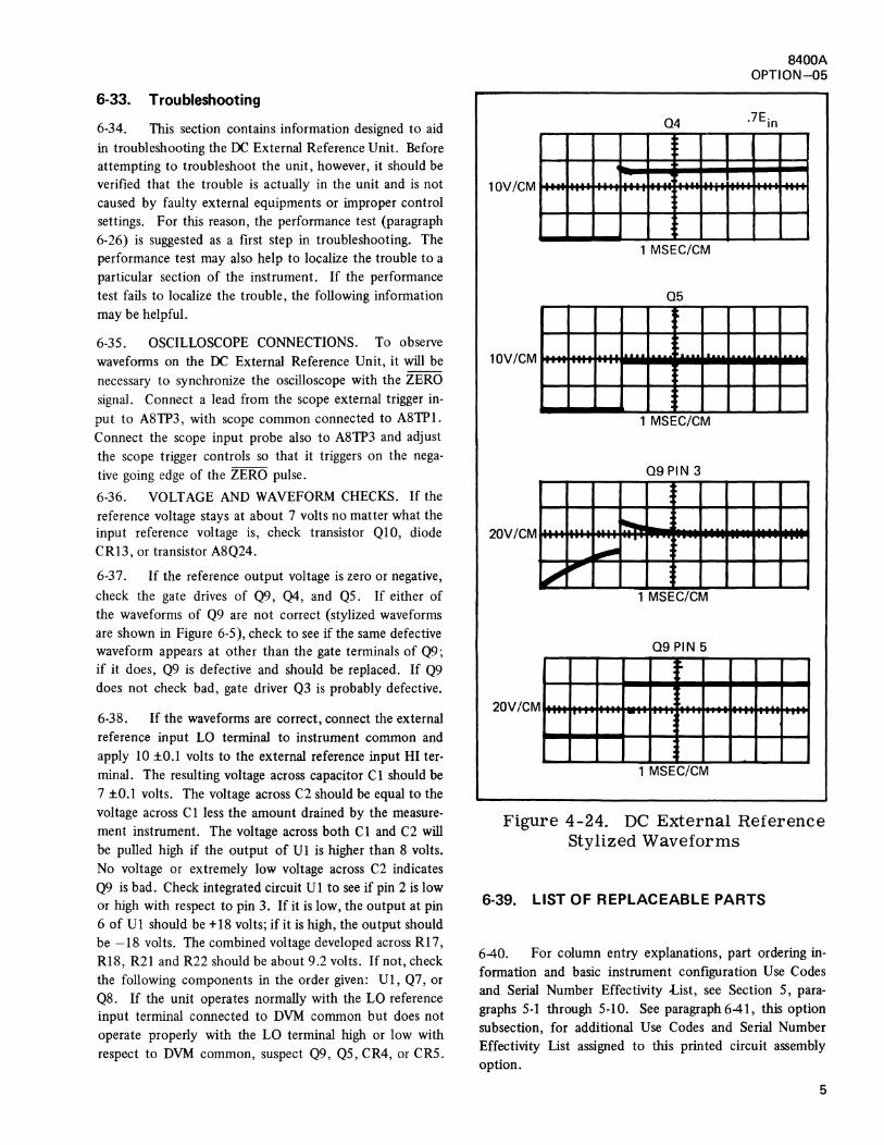
6-33. Troubleshooting
6-34. This section contains information designed to aid in troubleshooting the OC External Reference Unit. Before attempting to troubleshoot the unit, however, it should be verified that the trouble is actually in the unit and is not caused by faulty external equipments or improper control settings. For this reason, the performance test (paragraph 6-26) is suggested as a first step in troubleshooting. The performance test may also help to localize the trouble to a particular section of the instrument. If the performance test fails to localize the trouble, the following information may be helpful.
6-35. OSCILLOSCOPE CONNECTIONS. To observe waveforms on the OC External Reference Unit, it will be necessary to synchronize the oscilloscope with the ZERO signal. Connect a lead from the scope external trigger input to A8TP3, with scope common connected to A8TP1. Connect the scope input probe also to A8TP3 and adjust the scope trigger controls so that it triggers on the negative going edge of the ZERO pulse.
6-36. VOLTAGE AND WAVEFORM CHECKS. If the reference voltage stays at about 7 volts no matter what the input reference voltage is, check transistor QlO, diode CR13, or transistor A8Q24.
6-37. If the reference output voltage is zero or negative, check the gate drives of Q9, Q4, and Q5. If either of the waveforms of Q9 are not correct (stylized waveforms are shown in Figure 6-5), check to see if the same defective waveform appears at other than the gate terminals of Q9; if it does, Q9 is defective and should be replaced. If Q9 does not check bad, gate driver Q3 is probably defective.
6-38. If the waveforms are correct, connect the external reference input LO terminal to instrument common and apply 10 ±0.1 volts to the external reference input HI terminal. The resulting voltage across capacitor Cl should be 7 ±0.1 volts. The voltage across C2 should be equal to the voltage across C 1 less the amount drained by the measurement instrument. The voltage across both C 1 and C2 will be pulled high if the output of Ul is higher than 8 volts. No voltage or extremely low voltage across C2 indicates Q9 is bad. Check integrated circuit Ul to see if pin 2 is low or high with respect to pin 3. If it is low, the output at pin 6 of U1 should be + 18 volts; if it is high, the output should be -18 volts. The combined voltage developed across Rl7, Rl8, R21 and R22 should be about 9.2 volts. If not, check the following components in the order given: Ul, Q7, or Q8. If the unit operates normally with the LO reference input terminal connected to DVM common but does not operate properly with the LO terminal high or low with respect to DVM common, suspect Q9, Q5, CR4, or CR5.
10V/CM •• LL rr rr
10V/CM l_._ 1._._ •• .... .,...... ~
20V/CM LL•• .. '. U..LL rr
I.-
~ ~
20V/CM ""' IT ...... .........-
04 F'
La_.._ ·~~ ...... u..i.a. [TT'"•: .,.. ~ ..... r" .....
1 MSEC/CM
05 l
.. .... L1.
• 1 MSEC/CM
09PIN 3
..... 'I
~ l
1 MSEC/CM
09 PIN 5
~
r- " : __.
1 MSEC/CM
8400A OPTION-05
L_._ L._ .... .....
............. U<>~
,....,
ci, .. rr
Figure 4-24. DC External Reference Stylized Waveforms
6-39. LIST OF REPLACEABLE PARTS
6-40. For column entry explanations, part ordering information and basic instrument configuration Use Codes and Serial Number Effectivity List, see Section 5, paragraphs 5-1 through 5-10. See paragraph6-41, this option subsection, for additional Use Codes and Serial Number Effectivity List assigned to this printed circuit assembly option.
5

8400A OPTION-05
6
Figure 6-6. DC EXTERNAL REFERENCE

REF DESIG DESCRIPTION
A3 DC EXTERNAL REFERENCE Figure 6-6
Cl Cap, plstc, 0.1 uf ±20%, l 20Y
C2 Cap, plstc, 0.4 7 uf ±20%, l 20Y
C3 Cap, mica, 100 pf ±S%, SOOY
C4 Cap, mica, 4 7 pf ±S%, SOOY
CS,C7,C8 Cap, mica, 220 pf ±S%, SOOY
C6 Cap, plstc, 0.047 uf ±10%, 120Y
C9 Cap, mica, 33 pf ±S%, SOOY
CR1,CR2, CR4,CR6, CR7, CR8, Diode, silicon, lSO mA, 12S piv
CR9
CR3 Diode, fast switching, germanium, 40 mA, SO piv
CRS Diode, zener, S.lY
CRlO, CRl~ Diode, germanium, 80 mA, 100 piv
CR11,CR12 Diode, silicon, lSO mA
Fl, F2 Fuse, pigtail, l S mA, l 2SY (F2 fuse is a spare)
Kl Relay, Reed switch Coil, relay
Ql, Q6, QH~ Tstr, silicon, PNP
Q2, Q3, Q7 Tstr, silicon, NPN
Q4,QS Tstr, J-FET, N-channel
QB Tstr, silicon, NPN, Super beta dual monolithic
Q9 Tstr, FET, dual, P-channel
Rl Res, comp, 4.7k ±S%, l/4w
R2 Res, comp, 33k±S%, l/4w
R3,RS Res, set, ext ref, divider
R4, R20 Res, var, cermet Sk ±20%, l/2w
R6 Not used
R7,R8,R13 Res, comp, 22k ±S%, 1/4w
R9 Res, comp, 6.8k±S%, l/4w
RlO, R28 Res, comp, 12k ±S%, I /4w
10/18/74
STOCK NO
[t> 167460
190SS3
148494
148S36
170423
260S62
160317
2722S2
180SOS
1S9780
149187
203323
28S031
219097 269019
19S974
218396
271924
28407S
268011
148072
1481SS
278309
267872
148130
148098
1S9731
TOT
IOTY
REF
1
1
1
1
3
1
1
7
1
1
2
2
2
1 1
3
3
2
1
1
1
1
1
2
3
1
2
8400A OPTION-05
REC USE QTY CODE
7

8400A OPTION-05
REF DESIG
Rl 1
R12
R14
R15
R16
DESCRIPTION
Res, comp, 120k±5%, 1/4w
Res, comp, 2.2M ±5%, 1/4w
Res, comp, 180k±5%, 1/4w
Res, var, cermet, lk ±10%, 1 w
Res, met flm, l.54k ±1 %, 1/8w
STOCK NO TOT REC USE
~TY QTY CODE
193458 1
198390 1
193441 1
285155 1
289066 1
R17, R21 Res, selected in test (Rl 7 not shown on art) D> 2
R18, R22 Res, met flm, 215k±l%, 1/8w 289470 2
R19 Res, met flm, 2k±1%, l/8w 235226 1
R23 Res, met flm, 140k±1%, 1/8w 289439 1
R24 Res,metflm, 7.15k±l%, 1/8w 260356 1
R25 Res, met flm, 82.Sk ±1 %, 1 /8w 246223 1
R26 Res, met flm, 8.66k ±1 %, 1/8w 260364 1
R27 Res, comp, lk ±5%, l/4w 148023 1
R29, R30, Res, comp, lOOM ±10%, 1/2w 190520 3 R32
R31 Res, comp, 4.7M ±10%, 1/2w 108308 1
Ul IC, operational amplifier 271502 1
XFl Fuse holder 296582 2
Cable, Ref, input 304030 1
Terminal, teflon, feed thru, 4 lead 281865 4
[> Rl 7 and R21 factory selected at time of test.
G:> This option is not field installable in main-frame S/N 634 and below.
6-41. SERIAL NUMBER EFFECTIVITY
642. A Use Code column is provided to identify certain parts that have been added, deleted, or modified during production of the Model 8400A. Each part in this option for which a use code has been assigned may be identified with a particular printed circuit board serial number by consulting the Use Code Effectivity List below. All parts with no code are used on all printed circuit boards with
8
serial numbers 123 and on. NOTE: These Use Codes and Serial Number Effectivity apply to this option printed circuit board assembly only. For the standard instrument configuration, see Section 5, paragraph 5-9, and for additional options, see the appropriate option subsection.
USE CODE SERIAL NUMBER EFFECTIVI1Y
10/18/74
8400A OPTION-06
Option-06
AC External Reference
6-1. INTRODUCTION
6-2. The A4 AC External Reference Converter (Draw
ing No. 8400A-1008) when used in conjunction with the Al3 AC Converter and the 8400A DVM provides three
terminal ac to ac voltage ratio measurement capability through three ranges of 1, 10, and 100. The AC External Reference Converter rectifies the ac input voltage to a de voltage which becomes the instrument reference voltage.
6-3. SPECIFICATIONS
6-4. Specifications for the AC External Reference Con-verter are located in Section 1 of the manual.
6-5. INSTALLATION
6-6. The following procedure should be used to install
the AC External Reference Converter option in the Model 8400A.
a.
b.
c.
d.
NOTE
The AC External Reference option is not field installable in 8400A mainframes serial No. 634 and below.
Disconnect power cord from line power.
Remove the Model 8400A top dust cover and inner guard chassis cover.
Determine that connector J4 on A 14 Display board
is clear of obstructions and that alignment keys are inserted between pin pairs J4-l, -2; J4-3, -4 and J4-15, -16; J4-17,-18.
Remove connector mounting bracket located on rear portion of inner chassis, next to power transformer.
10/18/74
e.
f.
g.
h.
i.
j.
k.
6-7.
Mount the AC External Reference Converter connector to the connector bracket with orientation as shown on the rear panel decal. The lug attached to pin 1 of connector is to be mounted to the guard chassis through one of the mounting screws on the DC External Reference Connector.
Remount connector bracket back to the inner chassis.
Align AC External Reference Converter board with
vertical card guides mounted on inner chassis bulkhead.
Align rubber grommet with slot in rear inner chassis and slide grommet into slot.
Slide AC External Reference Converter board downward while observing that alignment keys in J4 are in proper alignment with the slots in the printed circuit board.
Engage printed circuit board fully in J4 connector.
Attach guard and top dust covers, connect power cord to line power, and perform receiving inspection test of DC External Reference assembly as described in paragraph 6-22, Performance Test.
OPERATING INSTRUCTIONS
6-8. Operation of the DVM with the A4 AC External
Reference Converter Option 8400-06 installed is covered in Section 2, Operating Instructions.

8400A OPTION-06
IOPERATIONALAECTIFIER ~
TRANSCONDUCTANCE AMPLIFIER
~-------DC DIFFERENCE AMPLIFIER/INTEGRATOR ---...,
R4 R5
R38 LOAD
RESISTOR
I I I I
~ R3? -18V~+18V
FRONT PANE l ZERO
SWITCH CLOSURES
~~ } EXT REF, VAC
RANGE
Figure 6-1. BLOCK DIAGRAM AC EXTERNAL REFERENCE CONVERTER.
6-9. THEORY OF OPERATION
6-10. General
6-11. The A4 AC External Reference Converter consists of two basic parts as shown in Figure 6-1: an operational rectifier and a de difference amplifier integrator. The operational rectifier consists of an inverting trans-conductance amplifier and load resistor with negative feedback arranged to provide a loop gain of about 5 x 10³ at midband. The feedback is changed with switch S 1 for range purposes. The input resistor is 1.11 megohms and provides 1.11 megohm input impedance at the AC Ext. Ref. input jacks. A symmetrical half-wave rectifier placed between the amplifier and load resistor develops equal positive and negative de voltages proportional to the amplifier output current. At full scale, this current is near two milliamps. The two output waveforms are shown in Figure 6-2.
2
ov
ov
I I I I I
+OUTPUT ~ :q : <==>'I c:::::=-::> I
I I I I I I
I I I I I ---0-U-TP_U_T-:v,v.---
I I I I I
Figure 6-2. RECTIFIER OUTPUT WAVEFORMS
6-12. The de difference amplifier/integrator filters the output waveforms of Figure 6-2 and amplifies the difference between them by a factor of 3 .33, providing a buffered voltage which becomes the instrument reference voltage. A minimum three sections of filtering are provided at all times.

6-13. Circuit Description
6-14. OPERATIONAL RECTIFIER. Input FET Ql functions as a source follower, while transistor Q2 provides a low impedance guard voltage which is used to bootstrap most of the capacity that otherwise would appear between the FET gate and circuit common. The first two differential pairs are in dual in-line package Ul. Together with Q4 and QS, they develop the required gain. Transistors Q3 and Q6 function as current sources, with values such that clipping due to overload is symmetrical. Changes in capacitor charges are small and amplifier recovery time is minimized. Transistor Q7 compensates for capacitance losses in the diodes.
6-15. DC-DIFFERENCE AMPLIFIER/INTEGRATOR. The filter network, which provides the input to the amplifier/integrator, consists of resistors R39, R40, R41, R43, R44, R45 and capacitors C 19, C20, C21, C22. Capacitors Cl9, C21,and C23 form matched pairs with capacitors C20, C22, and C24, respectively, to maintain good common-mode rejection. Gain for the de amplifier is provided by monolithic operational amplifier U2, thereby providing a total loop gain at de of about 5 x 10⁵ •
6-16. RANGE AND FUNCTION CONTROL. The A4 AC External Reference Converter input and output relays, Kl and K2, are driven by the combination of front panel pushbuttons and Q8. The range control of the External Reference Converter is controlled by switch SIA, B, and C for selection of ranges 1, 10, 100. Transistor Q 10 provides an interlocking feature which prevents the AC External Reference Converter from operating on any function but V AC. Switch Sl has a fourth position (DC ONLY) which prevents the AC External Reference from operating under any circumstances. This feature allows AC/DC ratios to be measured without removing the AC Ext. Ref. option from the mainframe, and the DC External Reference option is present.
6-17. MAINTENANCE
6-18. Introduction
6-19. This section contains maintenance information specifically intended for the AC External Reference Converter. Factory service information and general instructions regarding instrument access and cleaning are located in Section 4 of the Manual.
8400A OPTION-06
6-20. Test Equipment
6-21. The following equipment is recommended for testing, troubleshooting, and calibrating the AC External Reference Converter. If the recommended equipment is not available, equivalent or better instruments may be substituted.
EQUIPMENT NOMENCLATURE
AC Voltage Source
RECOMMENDED EQUIPMENT
HP Model 745A AC Calibrator with companion 1000 volt amplifier.
Multimeter Fluke Model 8 lOOA Digital Multimeter
Oscilloscope Tektronix Model 547
Oscilloscope Tektronix Model IAl Plug-In
6-22. Performance Test
6-23. The performance test in this section compares the AC External Reference Converter performance to the accuracy specifications in Section 1 of the manual to determine if the converter is in calibration. To test the unit, a reference voltage is applied to the AC External Reference input terminals, an ac voltage is applied to the DVM INPUT Terminals, and proper DVM readout is verified. The performance test should be conducted before any instrument maintenance or calibration is attempted. The test is also suited to receiving inspection of new units. The performance test should be conducted under the following environmental conditions after 1 hour warm up: ambient temperature
23°C ±5°C, relative humidity less than 70%. An instrument that fails the performance test will require corrective maintenance or calibration. In case of difficulty, analysis of the test results with reference to the troubleshooting section, should help to locate the trouble.
NOTE!
Permissible tolerances for ac voltage measurements are derived from the 90-day instrument specifications contained in Section 1 of the manual.
3
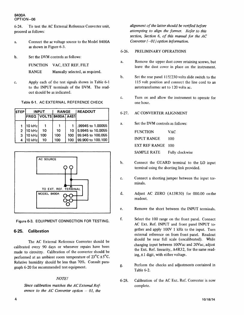
8400A OPTION-06
6-24. To test the AC External Reference Converter unit, proceed as follows:
a. Connect the ac voltage source to the Model 8400A as shown in Figure 6-3.
b. Set the DVM controls as follows:
c.
FUNCTION VAC, EXT REF, FILT
RANGE Manually selected, as required.
Apply each of the test signals shown in Table 6-1 to the INPUT terminals of the DVM. The readout should be as indicated.
Table 6-1. AC EXTERNAL REFERENCE CHECK
STEP INPUT RANGE READOUT FREQ VOLTS 8400A A4S1
1 10 kHz 1 1 1 .99945 to 1.00055
2 10 kHz 10 10 10 9.9945 to 10.0055 3 10 kHz 100 100 100 99.945 to 100.055 4 10 kHz 10 100 100 99.900 to 100.100
AC SOURCE
MODEL 8400A
Figure 6-3. EQUIPMENT CONNECTION FOR TESTING.
6-25. Calibration
The AC External Reference Converter should be calibrated every 90 days or whenever repairs have been made to circuitry. Calibration of the converter should be performed at an ambient room temperature of 23°C ±5°C. Relative humidity should be less than 70%. Consult paragraph 6-20 for recommended test equipment.
4
NOTE!
Since calibration matches the AC External Ref erence to the AC Converter option - 01, the
6-26.
a.
alignment of the latter should be verified before attempting to align the farmer. Refer to this section, Section 6, of this manual for the AC Converter (-01) option information.
PRELIMINARY OPERATIONS
Remove the upper dust cover retaining screws, but leave the dust cover in place on the instrument.
b. Set the rear panel 115/230 volts slide switch to the 115 volt position and connect the line cord to an autotransformer set to 120 volts ac.
c. Turn on and allow the instrument to operate for one hour.
6-27. AC CONVERTER ALIGNMENT
a. Set the DVM controls as follows:
FUNCTION V AC
INPUT RANGE 100
EXT REF RANGE 100
SAMPLE RATE Fully clockwise
b. Connect the GUARD terminal to the LO input terminal using the shorting link provided.
c. Connect a shorting jumper between the input terminals.
d. Adjust AC ZERO (Al3RSO) for 000.00 onthe readout.
e. Remove the short between the INPUT terminals.
f. Select the 100 range on the front panel. Connect AC Ext. Ref. INPUT and front panel INPUT together and apply lOOV 1 kHz to the input. Turn external reference on from front panel. Readout should be near full scale (uncalibrated). While changing input between lOOVac and 20Vac, adjust the Ext. Ref. linearity, A4R32, for the same reading,±1 digit, with either voltage.
g. Perform the checks and adjustments contained in Table 6-2.
6-28. Calibration of the AC Ext. Ref. Converter is now complete.
10/18/74

STEP
1
2 3
4
5
6 7 8 9
10
Table 6-2. AC EXTERNAL REFERENCE CONVERTER RANGE CALIBRATION
INPUT RANGE ADJUSTMENT READING
FREQ VOLTS 8400A Sl TOLERANCE
1 kHz 100.000 100 100 lOOV 1 kHz IA4R47) 99.995 to 100.005
50 kHz 100.000 100 100 lOOV 50 kHz IA4C21 99.995 to 100.005
20 kHz 100.000 100 100 Cln-'Lk Only 99.995 to 100.005
1 kHz 10.0000 10 10 lOV 1 kHz (A4R51 9.9995 tn 10.0005
50 kHz 10.0000 10 10 lOV 50 kHz (A4C41 9.9995 to 10.0005
100 kHz 10.0000 10 10 Check Only 9.9800 to 10.0200
1 kHz 1.0000 1 1 1V 1 kHz (A4R31 99995 to 1.00005
50 kHz 1.0000 I 1 1V 50 kHz IA4C3i 99995 to 1 .00005
100 kHz 1.0000 1 1 Check Only 99800 to 1 .00200
20 kHz 1.0000 1 1 Check Only .99995 to 1.00005
6-29. Troubleshooting
6-30. This section contains information selected to aid in
troubleshooting the AC External Reference Converter. Before attempting to troubleshoot the unit, however, it should be verified that the trouble is actually in the converter and is not caused by faulty external equipment or improper control settings. For this reason, the performance test (paragraph 6-22) is suggested as a first step in troubleshooting. The performance test may also help to localize trouble to a particular section of the instrument. If the performance test fails to localize the trouble, the following information may be helpful.
6-31. POWER SUPPLY VOLTAGE CHECK
6-32. In this test, each of the supply voltages for the AC External Reference Converter is checked at the pin connectors. This test verifies only presence of voltages; a detailed check of the DVM power supply voltages is given in Section 4.
a.
10/18/74
Connect the oscilloscope common to TP2 of the
converter. Use the internal de oscilloscope trigger.
Set the scope controls for de voltage measurement, and check the following voltages:
Connector Pin No.
3
Required Voltage
-18 volts +18 volts
6-33.
a.
b.
c.
8400A OPTION-06
SEVERE CONVERTER MALFUNCTIONS
Symptom:
Procedure:
Symptom: Procedure:
Symptom:
Procedure:
Full-scale output with shorted in
put. If de voltage at TP3 and ac voltage on TP2 are zero, then troubleshoot converter output difference ampli
fier/integrator, and associated circuits.
If the de voltage on TP3 is greater
than ±lV (normal is less than 10 m V) check for defective Q 1 through
Q6, Ul, C 11, C21 or associated
circuits.
If ac voltage is present on TP2,
check for open or shorted feedback circuit or defective component in amplifier causing oscillation.
Zero output with input applied. If ac voltage on TP2 is zero, check for open or short in ac circuit between input and QI.
If ac voltage does appear on TP2
(full scale is approximately 0.25V rms) check Sl or troubleshoot output difference amplifier/integrator.
Range of operation does not correspond to range selected. Check Sl for proper range selection.
6-34. LIST OF REPLACEABLE PARTS
6-35. For column entry explanations, part ordering in
formation and basic instrument configuration Use Codes and Serial Number Effectivity, see Section 5, paragraphs 5-1 through 5-10. See paragraph 6-36, this option subsection, for additional Use Codes and Serial Number Effectivity List
assigned to this printed circuit assembly option.
5
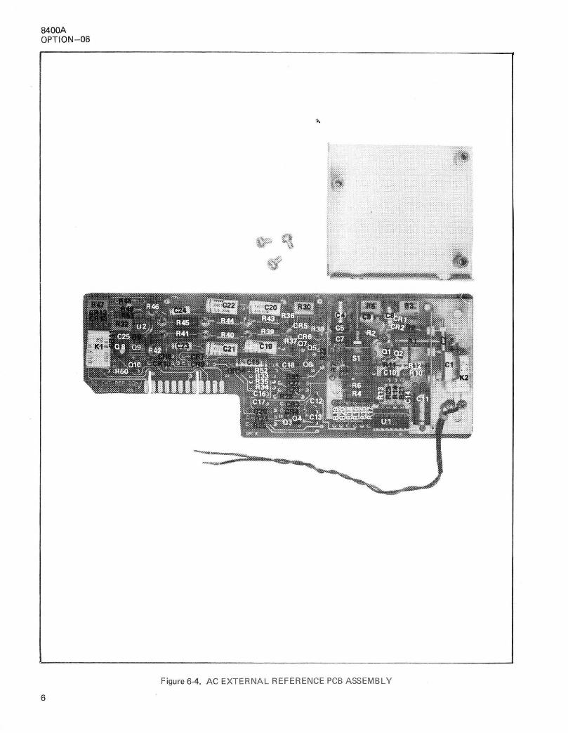
8400A OPTION- 06
6
Figure 6-4. AC EXTERNAL REFERENCE PCB ASSEMBLY
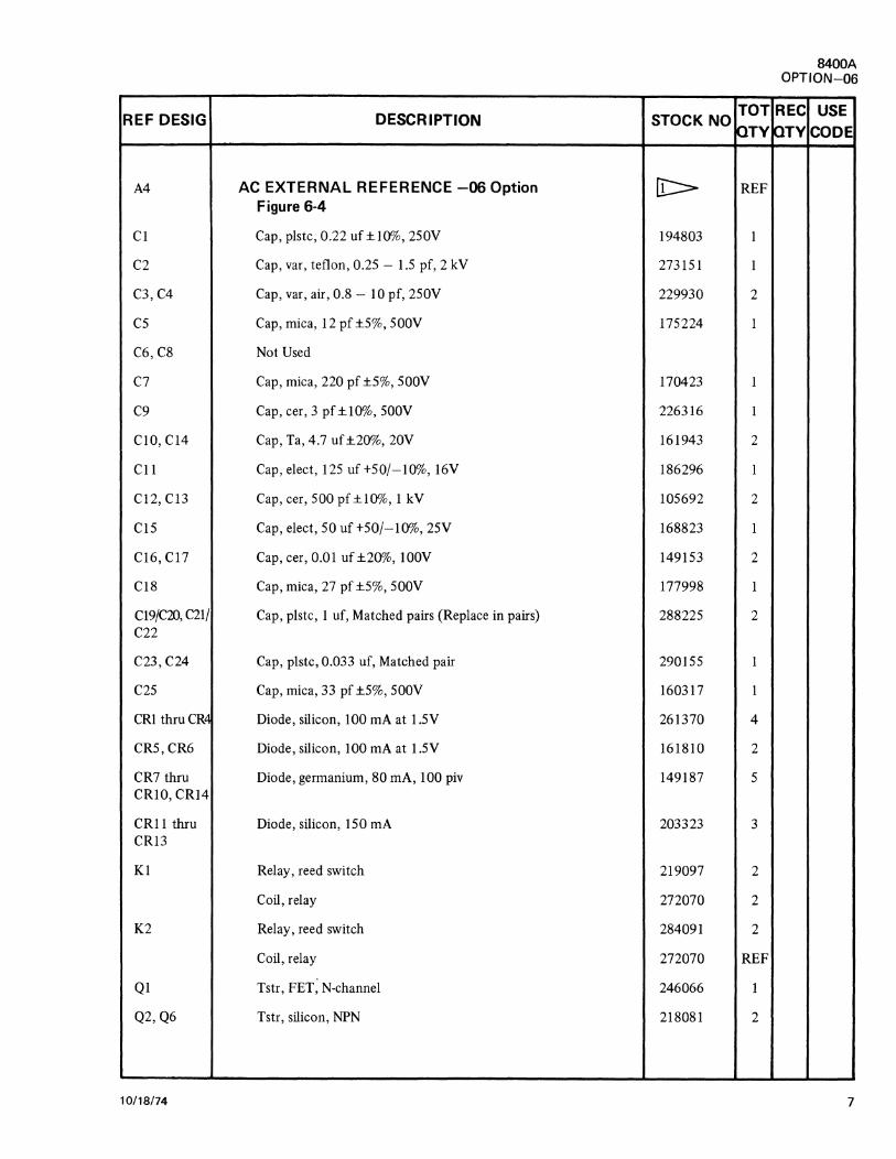
REF DESIG DESCRIPTION
A4 AC EXTERNAL REFERENCE -06 Option Figure 6-4
Cl Cap, plstc, 0.22 uf ±10%, 250V
C2 Cap, var, teflon, 0.25 - 1.5 pf, 2 kV
C3,C4 Cap, var, air, 0.8 - 10 pf, 250V
cs Cap, mica, 12 pf±5%, SOOV
C6,C8 Not Used
C7 Cap, mica, 220 pf ±5%, SOOV
C9 Cap, cer, 3 pf±l0%, SOOV
Cl0,Cl4 Cap, Ta, 4.7 uf ±20%, 20V
Cl l Cap, elect, 125uf+S0/-10%,16V
Cl2, C13 Cap, cer, 500 pf ±10%, 1 kV
Cl5 Cap, elect, 50 uf+S0/-10%, 25V
Cl6, C17 Cap, cer, 0.01 uf±20%, lOOV
Cl8 Cap, mica, 27 pf ±5%, SOOV
Cl9/C20, C21/ Cap, plstc, 1 uf, Matched pairs (Replace in pairs) C22
C23,C24 Cap, plstc, 0.033 uf, Matched pair
C25 Cap, mica, 33 pf ±5%, SOOV
CRl thruCR4 Diode, silicon, 100 mA at 1.SV
CR5,CR6 Diode, silicon, 100 mA at 1.SV
CR7 thru Diode, germanium, 80 mA, 100 piv CRlO, CR14
CRl l thru Diode, silicon, 150 mA CR13
Kl Relay, reed switch
Coil, relay
K2 Relay, reed switch
Coil, relay
Ql Tstr, FET, N-channel
Q2,Q6 Tstr, silicon, NPN
10/18/74
STOCK NO
[!:::>-
194803
273151
229930
175224
170423
226316
161943
186296
105692
168823
149153
177998
288225
290155
160317
261370
161810
149187
203323
219097
272070
284091
272070
246066
218081
TOT
iOTY
REF
1
1
2
1
1
1
2
1
2
1
2
1
2
1
1
4
2
5
3
2
2
2
REF
1
2
8400A OPTION-06
REC USE
iOTV CODE
7

8400A OPTION-06
REF DESIG
Q3, Q4, QS, Q7
Q8
Q9, QlO
Q9, QlO
Rl
R2
R3
R4
RS
R6
R7
R8
R9
RlO
Rl 1, R26
Rl2, R33, RS~
R13
R14
R15, R18
R16, Rl 7
R19, R20
R21, R22
R23
R24, R28
R25, R27
R29
R30, R32
R31
R34
8
DESCRIPTION
Ts tr, silicon, PNP
Tstr, silicon, PNP, selected
Tstr, silicon, NPN
Tstr, silicon, NPN
Res, met flm, 1.llM Matched Set
Res, met flm, 276k
Res, var, cermet, 2k ±10%, lw
Res, ww, 29.53k ±0.1%, Yzw
Res, var, cermet, 200.Q ±10%, lw
Res, ww, 2.573k±0.1%, Yzw
Res, met flm, 10.Q ±1%, 1/8w
Res, comp, 620.Q± 5%, %w
Res, met flm, 49.9k ±1%, 1/8w
Res, comp, 8.2k ±5%, %w
Res, met flm, 590.Q ±1%, 1/8w
Res, comp, lOk ±5%, %w
Res, comp, 15k ±5%, %w
Res, met flm, 84.Sk ±0.5%, 1/8w
Res, comp, 120k ±5%, %w
Res, comp, l lk ±5%, %w
Res, comp, 47.Q ±5%, %w
Res, met flm, 40.2k ±1%, 1/8w
Res, met flm, 82.Sk ±1%, 1/8w
Res, met flm, 10k±l%, 1/8w
Res, met flm, 21.Sk ± 1 %, 1 /8w
Res, met flm, 1.21k ±1%, 1/8w
Res, var, cer met lOOk ± 10%, 1 w
Res, comp, lOM ±5%, %w
Res, comp, 22k ±5%, %w
STOCK NO TOT REC USE
lclTY IOTY CODE
229898 4
280198 1
218396 2 A
168708 2 B
269092 1
285163 1
277657 1
285148 1
277665 1
268789 1
221903 1
268821 1
160796 1
261883 2
148106 3
148114 1
229492 1
193458 2
221580 2
147892 2
235333 2
246223 1
168260 2
168278 2
229146 1
288308 2
194944 1
148130 1
10/18/74

REF DESIG DESCRIPTION
R35 Res, comp, 2.2k ±5%, 14w
R36, R37 Res, ww, I .l 96k ±O.I%, 14w
R38 Res, ww, I 2Sn ±0.l %, 14w
R39, R40, Res, ww, I30k ±O.I%, %w R43, R44
R4I, R45 Res, ww, 40k ±0.1%
R42,R46 Res, ww, IM ±0.1%
R47 Res, var, cermet, 10k±IO%, Iw
R48 Res, met flm, 10on ±I%, I/8w
R49 Res, met flm, 487k ± 1%, I/8w
RSO Res, comp, 430n ±5%, 14w
RSI Res. comp. 6.2k t.5%, 14w RS3 Res, comp, 120kt5%, 14w RS4 Res, comp, 120kt5%, 14w SI Switch, rotary Ul IC, 5-Transistor Array
U2 IC, operational amplifier
Socket, IC, 14 contact, U1
STOCK NO TOT
IOTV
I48049 I
2996IO 2
249284 I
28536I 4
27I403 2
27I4I I 2
28SI7I I
I68I95 I
237206 I
203869 I
22I9II I 193458 2 I93458 Ref 295535 I 248906 I
288928 I
276527 1
8400A OPTION-06
REC USE
IOTV CODE
D D c
[!:::::::>- This option is not field installable in mainframes
S/N 634 and below.
6-36. SERIAL NUMBER EFFECTIVITV
A Use Code column is provided to identify certain
parts that have been added, deleted, or modified during
production of the Model 8400A. Each part in this option for which a use code has been assigned may be identified
with a particular printed circuit board serial number by consul ting the Use Code Effectivity List below. All parts with
10/18/74
no code are used on all printed circuit boards with serial numbers 123 and on. NOTE: These Use Codes and Serial Number Effectivity apply to this option printed circuit board assembly only. For the standard instrument configuration, see Section 5, paragraph 5-9, and for additional
options, see the appropriate option subsection.
USE CODE
A
SERIAL NUMBER EFFECTIVITY
Serial number 123 thru 13 2.
B Serial number I33 and on.
C Serial number 123, I25, I28, 13I, I33 and on.
D Serial number I48 and on.
9


6-1. INTRODUCTION
6-2. The Rear Input Option provides INPUT HI, INPUT LO, Q SENSE, Q SOURCE and GUARD terminals at the rear of the instrument, in parallel with the front panel terminals.
6-3. INSTALLATION
6-4. The following procedure should be used to install the Rear Input Option:
a.
b.
Remove the instrument top dust and chassis guard covers.
Remove A13 AC CONVERTER from instrument if instrument is so optioned.
c. Remove connector bracket on inner chassis, right rear portion.
d.
e.
10/18/74
Mount Rear Input Connector onto the connector bracket top slot. Ensure that the lug which is attached to connector pin 2 is affixed to the inner guard chassis with one of the connector mounting screws.
Remount connector bracket to inner chassis.
f.
g.
h.
8400A OPTION-07
Option -07
Rear Input
Lay the Rear Input harness along side the Right side of the inner chassis and between the Al4 Display PCB and TBI. Clamp harness to inner chassis.
Connect Rear Input harness to terminals on rear of the front panel binding posts as follows:
RED - INPUT HI BLACK - INPUT LO YELLOW- HI Q SOURCE BROWN - LO Q SOURCE
Install the Al3 AC Converter if instrument is so optioned.
i. Attach guard and instrument dust cover.
6-5. LIST OF REPLACEABLE PARTS
6-6. For column entry explanations, part ordering information and basic instrument configuration Use Codes and Serial Number Effectivi ty List, see Section 5, paragraphs 5-1 through 5-10. See paragraph 6-7, this option subsection for additional Use Codes and Serial Number Effectivity List assigned to this option.

8400A OPTION-07
REF DESIG DESCRIPTION
REAR INPUT-07 Option
Cable, rear input
Hardware kit, option
Cable clamps
6-7. SERIAL NUMBER EFFECTIVITY
6-8. A Use Code column is provided to identify certain parts that have been added, deleted, or modified during production of the Model 8400A. Each part in this option for which a use code has been assigned may be identified with a particular printed circuit board serial number by consulting the Use Code Effectivity List below. All parts
2
STOCK NO TOT REC USE QTY QTY CODE
REF
311639 1
321661 1
165951 2
with no code are used on all Rear Input Options with serial numbers 123 and on. NOTE: These Use Codes and Serial Number Effectivity apply to this option assembly only. For the standard instrument configuration, see Section 5, paragraph 5-9, and for additional options, see the appropriate option subsection.
USE CODE
SERIAL NUMBER EFFECTIVITY
8400A OPTION -09
Option -09
True RMS Converter
6-1. INTRODUCTION AC ranges. A choice of input coupling for the True RMS Converter is available to the operator. Choosing ac coupling allows measurement of the ac component of the input voltage. Choosing direct coupling provides measurement of the ac plus de components.
6-2. Equipped with Option -09, the Model 8400A provides true rms measurement capabilities through the four
6-3. SPECIFICATIONS-------------------------
RANGES ..
Overrange .
Resolution .
Overload
For Measurement of DC-Coupled (AC+ DC) Voltages or AC Only.
1, 10, 100, 1000 VAC
20%, 1100V RMS maximum on 1000V range
0.001% range
11 OOV RMS any range ( 1500V peak AC)
Superimposed DC (AC only) 1100V DC (Peak AC plus DC may not exceed ±1500V)
Max. Crest Factor
ACCURACY
90 days,
(18°C to 28°C)
10.001 v . 110ov1111
7 at full-scale and increasing down scale per:
7X
V Range
V Input
AC+ DC AC ONLY
D.C. . :!:(0.1 % of input+ 0.03% of range)
50Hz-10kHz ±(0.1% of input+ 0.03% of range) ±(0. l% of input+ 0.012% of range)
10kHz-30kHz 121 ±(0.2% of input+ 0.06% of range) ±(0.2% of input+ 0.04% of range)
30kHz-50kHz121 ±(0.3% of input+ 0.12% of range) ±(0.3% of input+ 0.1 % of range)
20Hz-50Hz. ±(0.5% of input+ 0.03% of range) ±(0.5% of input+ 0.012% of range)
10Hz-20Hz. ±( 1.0% of input+ 0.06% of range) ±(1.0% of input+ 0.04% of range)
50kHz-100kHz!2l. ±(1.0% of input+ 0.3% of range) ±( 1.0% of input + 0.3% of range)
100kHz-300kHz 121 ±(2.0% of input+ 0.5% of range) ±(2.0% of input+ 0.5% of range)
(1) With inputs above 500V multiply accuracy by r2000V + Vinpu~ [ 2000V J
(2) Input volt x hertz, product should not exceed 2 x I o7.
Temperature Coefficients (0°C to 18°C and 28° C to 50°C)
DC and 10 Hz· 10 kHz (AC+ DC) . . ±(0.004% lnp. + 0.004% Range)
10 Hz· 10 kHz (AC only) . . ±(0.004% lnp. + 0.001% Range) Input Impedance . 1 Megohm, shunted by less than 150 p.f.
10/18/74
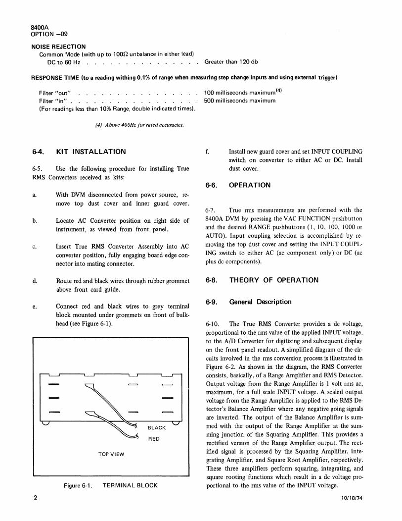
8400A OPTION -09
NOISE REJECTION Common Mode (with up to 100il unbalance in either lead)
DC to 60 Hz . . . . . . . . . . . . . . . Greater than 120 db
RESPONSE TIME (to a reading withing 0.1% of range when measuring step change inputs and using external trigger)
Filter "out" 100 milliseconds maximum14l Filter "in" . . . . . . . . . . . . . . . . . 500 milliseconds maximum (For readings less than 10% Range, double indicated times).
(4) Above 400Hz for rated accuracies.
6-4. KIT INSTALLATION
6-5. Use the following procedure for installing True
RMS Converters received as kits:
a. With DVM disconnected from power source, re
move top dust cover and inner guard cover.
b.
c.
d.
e.
2
Locate AC Converter position on right side of instrument, as viewed from front panel.
Insert True RMS Converter Assembly into AC
converter position, fully engaging board edge connector into mating connector.
Route red and black wires through rubber grommet above front card guide.
Connect red and black wires to grey terminal block mounted under grommets on front of bulk
head (see Figure 6-1).
TOP VIEW
=
BLACK
RED
Figure 6-1. TERMINAL BLOCK
f. Install new guard cover and set INPUT COUPLING switch on converter to either AC or DC. Install dust cover.
&6. OPERATION
6-7. True rms measurements are performed with the 8400A DVM by pressing the V AC FUNCTION pushbutton and the desired RANGE pushbuttons (1, 10, 100, 1000 or
AUTO). Input coupling selection is accomplished by removing the top dust cover and setting the INPUT COUPLING switch to either AC (ac component only) or DC (ac plus de components).
6-8. THEORY OF OPERATION
6-9. General Description
6-10. The True RMS Converter provides a de voltage, proportional to the rms value of the applied INPUT voltage, to the A/D Converter for digitizing and subsequent display on the front panel readout. A simplified diagram of the cir
cuits involved in the rms conversion process is illustrated in Figure 6-2. As shown in the diagram, the RMS Converter consists, basically, of a Range Amplifier and RMS Detector. Output voltage from the Range Amplifier is 1 volt rms ac, maximum, for a full scale INPUT voltage. A scaled output voltage from the Range Amplifier is applied to the RMS Detector's Balance Amplifier where any negative going signals are inverted. The output of the Balance Amplifier is summed with the output of the Range Amplifier at the summing junction of the Squaring Amplifier. This provides a rectified version of the Range Amplifier output. The rectified signal is processed by the Squaring Amplifier, Integrating Amplifier, and Square Root Amplifier, respectively. These three amplifiers perform squaring, integrating, and square rooting functions which result in a de voltage proportional to the rms value of the INPUT voltage.
10/18/74

"TI <C c .... ('!)
c;n r-v
-I :::0 c m :::0 $ CJ)
('") 0 z < m :::0 -I m :::0 OJ r 0 ('") 7\ 0 )> G) :::0 )> $
w
AC
IN
INPUT COUPLING SWITCH
DC
RANGE FEEDBACK
SQUARING AMPL. 0
OUTPUT
RESISTIVE PATH
RMS DETECTOR .................... ,_.,_.,_.,_.,_...,.
LOGARITHMIC FEEDBACK
LOGARITHMIC FEEDBACK
MUL Tl POLE RC FEEDBACK
R:~~~- O~,_ .. ...., .......... ,._ ........ ~ +BAL:~~~. o ..... 1-.. ---............. .._,_._..~ SQUARING AMPL. O ...... ._,_....,..,.,_._.,_.,_. ... -
OUTPUT OUTPUT INPUT 0 -0 ::! 0 zoo I~ oO co)>

8400A OPTION -09
6-11. Circuit Description
6-12. RANGE AMPLIFIER
6-13. The Range Amplifier scales the applied input voltage to the Converter to l volt rms ac for a full scale input. Basically, the Range Amplifier is an inverting operational amplifier whose gain changes as the range changes. Voltage gains of -1, -10, -100, and -1000 correspond with the 1 through 1000 volt ranges, respectively. Active elements of the Range Amplifiers are Ql, Q2, QS and U3 with protection diodes CR6, CR7, CR18, CR20, CR21, and CR22. Transistor Q2 drives the guard at the summing point of the operational amplifier, and QS switches CS into feedback path in the 10, 100, and 1000 volt ranges. Diodes CR6, CR7, CR21, and CR22 provide clipping for input overload protection to Ql. Diodes CR18 and CR20 provide overload clipping at the output of the Range Amplifier for protection of the following circuitry.
6-14. BALANCE AMPLIFIER
6-1 S. The Balance Amplifier is a rectifying amplifier with a gain of -1 that changes all negative going signals from the Range Amplifier output to positive voltages prior to summing with the Range Amplifier output from R33. Balance Gain adjustment (R32) controls the input to the Balance Amplifier, such that positive and negative signals at the summing junction of R3 l, R33 and US will be equal in magnitude. Active components of the Balance Amplifier are CR.lS, Q6, Q9, QlO, and U4. Balance Zero Adjustment, R42, is an adjustment for zeroing the input of U4. Primary or low frequency signal path is through U4 followed by CRl S and final output stage Q 10. At frequencies above a few hundred kilohertz, amplification takes place through Q6 followed by QlO. The final output stage, QlO, has a current source load, CLl, which maintains a high amplifier output impedance for driving CR14 and CR16. Any stray capacitance in CR14 and CR16 is compensated by Q9. Transistor Q9 samples the waveform driving CR14 and CR16 and feeds back a capacitive charge through C 17 to the input of the Balance Amplifier.
6-16. SQUARING AMPLIFIER
6-17. The Squaring Amplifier is an inverting operational amplifier with non-linear feedback through matched transistors Q8A and Q12A. These transistors transform the input current into an output voltage that is the logarithim of the input current. Since this operation is performed twice (by Q8A and Q12A), the output voltage is twice the log of
4
the input current. Therefore, the amplifier essentially accomplishes a squaring operation (2 log X = log x2). US is an integrated operational amplifier which is paralleled by Q7 at high frequencies in a manner similar to Q6 in the Balance Amplifier. AC Zero Adjustment, R4S, provides for zeroing of US, and has the greatest effect, of all other zero adjusts, for overall converter zero. Both amplifying paths, US and Q7, share the common final output stage, Qll. Output voltage from Qll is sampled by Q12B which provides a current to the summing point of the Integrator Amplifier. Potentiometer R38 provides an adjustment for crest factor gain.
6-18. INTEGRATOR AMPLIFIER
6-19. The Integrator Amplifier consists primarily of U7 and U8, and is a complex multipole integrator which acts as a three pole filter. Voltage at terminal 2 of U7 is held at zero, and all of the current applied is passed through the feedback elements RS6, R6S, and whichever feedback capacitors are switched into the circuit. Switchable capacitors are connected through FET's Ql3, Ql4, Ql6 and QI 7 by operation of the FILT switch on the instrument front panel. If the FILT/RMS DC switch is depressed, the FET's are turned on, and the capacitors are a part of the feedback circuitry. Since each switchable capacitor is paralleled by a non-switchable capacitor, some filtering action takes place in the Integrator Amplifier whether the FILT/RMS DC switch is depressed or not. Amplifier U7 and associated multipole feedback circuitry provides the integration for the Integrator Amplifier. Amplifier U8 is a unity gain, high input impedance, low output impedance amplifier. Three poles of feedback for U7 consist of C30, R68 and C32, and R69 and C33. Capacitor C29 can be switched in parallel with C30, C34 with C32, C3S with C33, and C28 with C27. Output from U8 is the output of the total Integrator Amplifier which is then applied to the A-to-D Converter and to the Square Root Amplifier.
6-20. SQUARE ROOT AMPLIFIER
6-21. The Square Root Amplifier consists of the input resistor R57, the trimming and selection resistors R61, R62, R63, and R64, the feedback transistor Q8B, protection diode CR19, and amplifier U6. Diode CR19 acts as a feedback path to prevent saturation of U6 should input polarity to the amplifier reverse. The Square Root Amplifier uses logarithmetric feedback to produce a square root of the input in a manner similar to that used by the Squaring Amplifier. The square root process is accomplished by matched transistors Q8B and Q12B. Resistors R48, R79, and R80 are factory selected for overall converter temperature coef-

ficient and linearity. Some or none of these resistors may be installed.
6-22. MAINTENANCE
6-23. Introduction
6-24. Maintenance information, described in the following paragraphs, is specifically intended for the True RMS Converter Assembly. Service information and general instructions regarding instrument access and cleaning are described in Section 4 of the Instruction Manual. Test equipment for calibrating and troubleshooting the True RMS Converter is listed in Table 6-1. If the recommended equipment is not available, equipment having, at least, equivalent specifications may be used.
6-25. Calibration
6-26. The True RMS Converter should be calibrated every 90 days, or whenever repairs have been made to circuitry. Calibration of the converter should be performed at an ambient temperature of 28°C ±5°C. Relative humidity should be less than 70%.
6-27. PRELIMINARY OPERATIONS
a. Remove top dust cover screws, but leave the cover in place.
b. Set rear panel 115/230 volt switch to 115 volt position. Connect line cord to autotransformer set to 120 volts ac.
c.
8400A OPTION -09
Turn instrument on and allow one hour for warmup.
6-28. RANGE AMPLIFIER ZERO
a. Short the HI and LO INPUT terminals. Select VAC, FILT, and 10 RANGE pushbuttons. Place AC-DC switch on RMS converter to DC. This switch is accessible through the top guard cover.
b.
NOTE!
For Option -09's without de coupling, connect jumper wire across input coupling capacitor Cl.
Connect high lead of external de voltmeter to body of Cl 1 ( 1 OV SO kHz adjustment) via a 1 Ok isolation resistor.Connect low lead to the 8400A LO INPUT terminal.
c. Adjust R12 (Range Zero Adjust) for external voltmeter indication ofO ± 30µV.
d. Remove external voltmeter and INPUT short.
6-29. BALANCE AMPLIFIER ZERO
a. Apply -0.l V de to INPUT terminals from de voltage source. Note 8400A reading.
b.
c.
d.
Reverse input voltage polarity to +0.1 V de.
Adjust R42 (Balance Zero Adjust) for reading noted in step a.
Repeat steps a and b until difference between readings for each polarity is within 10 digits.
Table 6-1. TEST EQUIPMENT
REQUIRED NOMENCLATURE SPECIFICATIONS RECOMMENDED EQUIPMENT
AC Voltage Source 1mV and 1000V @ SOOHz Fluke Model S200A AC Calibrator and S205A power Amplifier 1V, 10V, 1000V @ SOOHz and SOkHz ±o.03% 1000V @ SO kHz __ ±o.3%
DC Voltage Source 10V ±o.01% Fluke Model 341A DVM Calibrator
DC Differential Voltmeter 100µV Range ±o.OOS% Fluke Model 89SA Differential Voltmeter
RMS Differential Voltmeter 100Hz @ ±O.OS% Fluke Model 931 A True RMS Differtial Voltmeter Crest Factor of 10
Oscilloscope General Purpose Tektronix 544 W/Type L Plug-In and Low Capacitance Probe
Pulse Generator son Source Impedance, HP 8003A Pulse Generator SV max. across son,(+) and (-) pulse polarity, Rise and Fall Time <50 ns
10/18/74 5

8400A OPTION -09
6-30. BALANCE GAIN
a. Apply -lOV de to INPUT terminals. Note 8400A reading.
b. Reverse input voltage polarity to +lOV de.
c.
d.
Adjust R32 (Balance Gain Adjust) for 8400A reading equivalent to step a.
Repeat steps a through c until difference between readings for each polarity is within 10 digits.
e. Remove de voltage source.
6-31. AC ZERO
a. Select 1 RANGE and AC INPUT COUPLING.
Apply 0.001 volts at 500 Hz to INPUT terminals.
b. Adjust R45 (AC Zero Adjust) for reading of
.00100 ± 3 digits.
c. Remove ac input voltage.
6-32. CALIBRATION ADJUSTMENT/CHECK
6-33. Before performing calibration, allow one hour "warm-up" with outer covers installed. Refer to Table 6-2; apply each of the rms voltages at the specified frequencies
to the INPUT terminals and, if necessary, perform the indicated adjustments to complete the calibration. If R64 (lOOOV, 500Hz adjustment) is not within adjustment range, refer to paragraph titled "Course Calibration."
6-34. COURSE CALIBRATION
6-35. Use the following procedure only when R64 is out
of adjustment range.
a.
b.
Connect any opened shorting links (1, 2, or 4)
across course calibration resistors R61, R62 or R63.
Select the 1000 volt range and apply 500V @
500 Hz to the INPUT terminals.
c. Adjust the "lOOOV, 500 Hz" control (R64) for a
minimum reading.
d.
e.
Cut open the appropriate link or links as indicated
below depending upon the 8400A reading.
READING CUT LINKS
465.7 - 470.1 1, 2. 4
470.1 - 474.3 2,4
474.3 - 478.7 1, 4
478.7 - 482.5 4
482.5 - 486.9 1,2
486.9 - 491.1 2
491.1 - 495.5 1
495.5- 500 NONE
Repeat the "Calibration Adjustment/Check" paragraph to complete calibration.
6-36. Troubleshooting
6-37. The troubleshooting procedure presents a technique for isolating a malfunction to one of the five amplifier circuits within the RMS Converter. Troubleshooting procedures for the power supply, command voltages, and relays are located in Option -0 l troubleshooting section of the Instruction Manual. Before using any of these procedures, ensure that the malfunction is within the RMS Converter and not due to operator error, faulty test leads, etc. Refer to Figure 6-3 for location of adjustments and test
points.
Table 6-2. CALIBRATION ADJUSTMENT/CHECK
INPUT ADJUSTMENT
VOLTAGE FREQUENCY RANGE NAME REF DESIG. TOLERANCE (RMS VOLTS)
500.0 500Hz 1000 1000V 500Hz R64 500.0 50kHz 1000 1kV 50kHz C4 1.0000 500Hz 1 1V 500Hz R14 1.0000 50kHz 1 1V 50kHz C9 ±10 digits 10.000 500Hz 10 10V 500Hz R16 10.000 50kHz 10 10V 50kHz C11 100.00 500Hz 100 100V 500Hz R18 100.00 50kHz 100 100V 50kHz C14
6
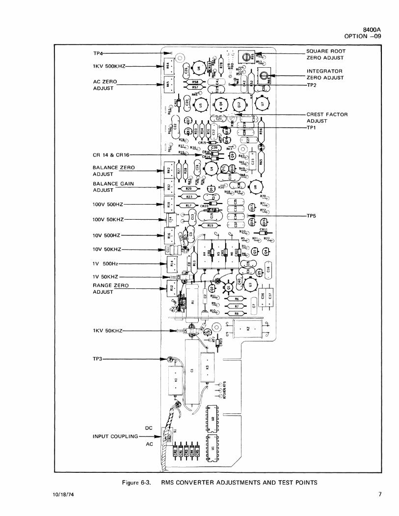
Figure 6-3. RMS CONVERTER ADJUSTMENTS AND TEST POINTS
8400A OPTION -09
10/18/74 7
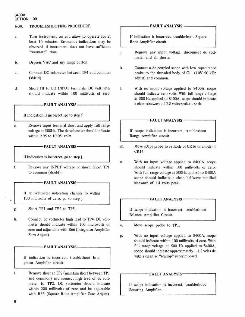
8400A OPTION -09
6-38. TROUBLESHOOTING PROCEDURE
a Turn instrument on and allow to operate for at least 10 minutes. Erroneous indications may be observed if instrument does not have sufficient "warm-up" time.
b. Depress V AC and any range button.
c.
d.
Connect DC voltmeter between TP4 and common
(shield).
Short HI to LO INPUT terminals. DC voltmeter should indicate within 100 millivolts of zero.
------FAULT ANALYSIS-------
e.
If indication is incorrect, go to step f.
Remove input terminal short and apply full range
voltage at SOOHz. The de voltmeter should indicate within 9.95 to 10.05 volts.
------FAULT ANALYSIS------
f.
If indication is incorrect, go to step j.
Remove any INPUT voltage or short. Short TPl to common (shield).
------FAULT ANALYSIS------...
g.
h.
If de voltmeter indication changes to within 100 millivolts of zero, go to step j.
Short TPl and TP2 to TPS.
Connect de voltmeter high lead to TP4. DC voltmeter should indicate within 100 microvolts of zero and adjustable with R66 (Integrator Amplifier Zero Adjust).
r-------FAULT ANALYSIS------
i.
8
If indication is incorrect, troubleshoot Integrator Amplifier circuit.
Remove short at TP2 (maintain short between TPl and common) and connect high lead of de voltmeter to TP2. DC voltmeter should indicate
within 200 millivolts of zero and be adjustable with RSS (Square Root Amplifier Zero Adjust).
-----FAULT ANALYSIS------
k.
l.
If indication is incorrect, troubleshoot Square Root Amplifier circuit.
Remove any input voltage, disconnect de voltmeter and all shorts.
Connect a de coupled scope with low capacitance probe to the threaded body of C11 (lOV SO kHz adjust) and common.
With no input voltage applied to 8400A, scope should indicate zero volts. With full range voltage at 500 Hz applied to 8400A, scope should indicate a clean sinewave of 2.8 volts peak-to-peak.
------FAULT ANALYSIS-------.
m.
n.
If scope indication is incorrect, troubleshoot Range Amplifier circuit.
Move sct>pe probe to cathode ofCR16 or anode of CR14.
With no input voltage applied to 8400A, scope should indicate within 100 millivolts of zero.
With full range voltage at SOOHz applied to 8400A
scope should indicate a clean halfwave rectified sinewave of 1.4 volts peak.
------FAULT ANALYSIS-------.
0.
p.
If scope indication is incorrect, troubleshoot Balance Amplifier Circuit.
Move scope probe to TPl.
With no input voltage applied to 8400A, scope should indicate within 100 millivolts of zero. With full range voltage at 500 Hz applied to 8400A, scope should indicate approximately -1.2 volts de with a clean ac "scallop" superimposed.
------FAULT ANALYSIS-------.
If scope indication is incorrect, troubleshoot Squaring Amplifier.
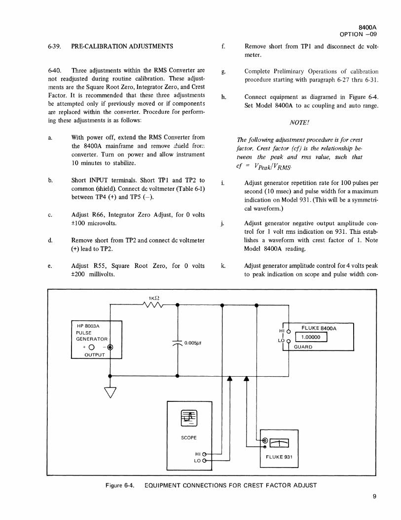
6-39. PRE-CALIBRATION ADJUSTMENTS
640. Three adjustments within the RMS Converter are not readjusted during routine calibration. These adjustments are the Square Root Zero, Integrator Zero, and Crest Factor. It is recommended that these three adjustments be attempted only if previously moved or if components are replaced within the converter. Procedure for performing these adjustments is as follows:
a.
b.
With power off, extend the RMS Converter from
the 8400A mainframe and remove 3hield fr01:: converter. Turn on power and allow instrument 10 minutes to stabilize.
Short INPUT terminals. Short TPI and TP2 to common (shield). Connect de voltmeter (Table 6-1) between TP4 ( +) and TPS (-).
c. Adjust R66, Integrator Zero Adjust, for 0 volts ±100 microvolts.
cl.
e.
Remove short from TP2 and connect de voltmeter (+)lead to TP2.
Adjust RSS, Square Root Zero, for 0 volts ±200 millivolts.
HP 8003A
PULSE GENERATOR
+ 0 -~~ OUTPUT
1K.Q
v
~ 0.005µf
SCOPE
f.
g.
h.
i.
j.
k.
HI (7,..,.,_.._...J
LO()-~+--...J
8400A OPTION -09
Remove short from TPI and disconnect de voltmeter.
Complete Preliminary Operations of calibration procedure starting with paragraph 6-27 thru 6-31.
Connect equipment as diagramed in Figure 6-4. Set Model 8400A to ac coupling and auto range.
NOTE!
The following adjustment procedure is for crest factor. Crest factor (cf) is the relationship between the peak and rms value, such that
cf = V Peakf V RMS·
Adjust generator repetition rate for 100 pulses per second (10 msec) and pulse width for a maximum indication on Model 931. (This will be a symmetri
cal waveform.)
Adjust generator negative output amplitude control for 1 volt rms indication on 931. This establishes a waveform with crest factor of 1. Note Model 8400A reading.
Adjust generator amplitude control for 4 volts peak
to peak indication on scope and pulse width con-
H~ 6 FLUKE 8400A
L6 ~ I 1.00000 I T GUARD
FLUKE 931
Figure 6-4. EQUIPMENT CONNECTIONS FOR CREST FACTOR ADJUST
9

8400A OPTION -09
l.
m.
n.
o.
p.
trol for 1 volt RMS indication on Model 931. This establishes a waveform with crest factor of 4.
Adjust R38 (Crest Factor Adjust) for Model 8400A indication noted in step j.
Repeat steps b through e until difference between readings for crest factors of 1 and 4 is less than 10 digits.
Check positive polarity pulse with crest factor of 4 by connecting equipment to pulse generator positive output and make adjustments described in step k.
8400A indication should be within 30 digits of finalized value noted in step j.
Turn power off. Disconnect all test equipment from 8400A. Re-install shield on RMS Converter and install the converter in 8400A mainframe. Install top guard and dust cover. Turn on instrument and allow to "warm-up" for one hour before performing Calibration Adjustment/Check, paragraph 6-30.
6-40. MATCHED COMPONENTS
6-41. A few components within the RMS Converter are matched at the factory. Two transistors, Q8 and Q9~ are matched to each other. Resistors R56, R76, and R77 are factory selected for overall converter temperatur~ coefficient and linearity which also affects Q8 and Q9. Should any of these components require replacement, a complete matched set will have to be ordered. In the case of replacement, the total set must be installed. Depending upon the
10
matched set received, some or none of the three resistors may be included. Therefore, in positions where there is no resistor to install, a bus wire must be installed. Refer to List of Replaceable Parts for ordering information.
6-42. LIST OF REPLACEABLE PARTS
6-43. For column entry explanations, part ordering information and basic instrument configuration Use Codes and Serial Number Effectivity List, see Section 5, paragraphs 5-1 through 5-10. See paragraph 6-44, this option subsection, for additional Use Codes and Serial Number Effectivity List assigned to this printed circuit assembly option.
6-44. SERIAL NUMBER EFFECTIVITY
645. A Use Code column is provided to identify certain parts that have been added, deleted, or modified during production of the Model 8400A. Each part in this option for which a use code has been assigned may be identified with a particular printed circuit board serial number by consulting the Use Code Effectivity List below. All parts with no code are used on all printed circuit boards with serial numbers 123 and on. NOTE: These Use Codes and Serial Number Effectivity apply to this option printed circuit board only. For the standard instrument configuration, see Section 5, paragraph 5-9, and for additional options, see the appropriate option subsection.
USE CODE
A
B
SERIAL NUMBER EFFECTIVITY
123 thru 54300
54400 and on.

REF DESIG DESCRIPTION
A22 RMS CONVERTER (-09 Option) Figure 6-
Cl Cap, piste, 0.22 uf ± 20%, 1200V
C2 Cap, pore, 2. 7 pf± 0.2S pf, l 700V
C3 Cap, mica, 220 pf ± S%, SOOY
C4,C9 Cap, var, teflon, 0.2S - 1.S pf, 2kY
cs Cap, mica, 22 pf± S%, SOOY
C6 Cap, mica, 8 pf± 10%, SOOY C6 Cap, mica, 4 pf ± I 0%, SOOY C7,C34 Cap, piste, 0.1 uf ± 10%, 2SOV
C8 Cap, pore, 2.2 pf± 0.2S pf, 1700Y
ClO Cap, pore, 27 pf± S%, SOOY
Cll Cap, var, air, 0.8- 10 pf, 2SOY
C12,C16, Cap, piste, 0.04 7 uf ± 10%, 2SOV C41,C42
C13 Cap, mica, 330 pf± 1 %, SOOY
C14 Cap, var, cer, 9 - 3S pf, 3SOY
ClS Cap, mica, 3600 pf± 2%, SOOY
C17 Cap, mica, 1 S pf ± S%, SOOY
C18,C20 Cap, mica, 27 pf ± S%, SOOY
Cl9,C22 Cap, mica, 1000 pf ± S%, SOOY
C21,C40 Cap, mica, 2 pf ± 0.5 pf, SOOY
C23,C36, Cap, Ta, 1 S uf ± 10%, 20Y C37
C24 Not Used
C2S Cap, mica, 390 pf± S%, SOOY
C26,C31, Cap, mica, 33 pf± S%, SOOV C38
C27,C30 Cap, piste, 6800 pf± 10%, 2SOY
C28,C29 Cap, piste, 0.022 uf± 10%, 2SOY
C32,C3S Cap, piste, 0.033 uf± 10%, 2SOV
C33 Cap, piste, 4 700 pf± 10%, 2SOY
STOCK NO
339309
268904
34074S
170423
218206
148SS1
216986 190397 161992
340273
344283
229930
162008
226142
289637
176644
148S69
177998
178387
17S208
1S30S6
148437
160317
342881
234484
234492
342873
TOT QTY
REF
1
1
1
2
1
1
2
1
1
1
4
1
1
1
1
2
2
2
3
1
3
2
2
2
1
8400A OPTION -09
REC USE QTY CODE
A B
11

8400A OPTION -09
REF DESIG
C39
CLl
CRl thru CR5
CR6,CR7, CR20
CR8,CR9, CRIO,CRll, CR17,CR23
CR12,CR13
CR14,CR16
CR15,CR18
CR19
CR21,CR22
Kl,K3
K2A,K2B, K4,K5,K6
Ql
Q2,Q6,Q7
Q3,Q101,Q18 Q9
Q4,Qll,Q15
Q5,Ql3,Q14 Ql6,Q17
Q8,Q12
RI
R2,Rll
R3,R4,R5, R47
R6,R7,R31
12
DESCRIPTION
Cap, piste, O.lµf± 10%, 250V
Current regulator FET
Diode, germanium, 80 mA, 100 piv
Diode, silicon, 100 mA at 1.SV
Diode, silicon, 150 mA
Not Used
Diode, silicon, 100 mA at l.5V
Diode, zener, lOV
Diode, silicon, 10 mA, 2 piv
Diode, zener, 6.8V
Relay, reed switch Coil, relay Foil wrap
Relay reed switch Coil, relay (K2) Coil, relay {K4,K5,K6) Foil wrap (K4,K5,K6)
Tstr, FET, dual, N-channel
Tstr, FET, N-~hannel
Tstr, silicon, NPN Tstr, sil, NPN
Tstr, silicon, PNP
Tstr, FET, N-channel
Part of matched set
Res, met flm, lM ± 0.1%, lw
Res, comp, 12k ± 5%, ~w
Res, comp, 51k ± 5%, ¥.iw
Res, met flm, 50k ± 0.1 %, 1/8w
STOCK NO TOT REC USE
IOTY IOTY CODE
161992 B
285106 1
149187 5
261370 3
203323 6
161810 2
246611 2
180554 1
260695 2
284091 2 269019 5 313833 2
289850 5 272070 1 269019 REF 280008 3
267963 1
343103 3
218396 3 218081 1 B
195974 3
288324 5
D> 1
340265 1
159731 2
193334 4
340257 3

REF DESIG DESCRIPTION
R8 Res, met flm, 48.7k ±I%, I/8w
R9,R20, Res, comp, IM ± 5%, %w R35,RS3, RS9,R67, R70
RIO Res, comp, 390.Q ± 5%, %w
RI2,R42, Res, var, cermet, IM± IO%, 0.w R45
RI3 Res, met flm, 99Sk ± O. I%, 0.w
RI4,R64 Res, var, cermet, lOk ± IO%, 0.w
RIS Res, met flm, I 10.6k ± O. I%, I/8w
RI6 Res, var, cermet, Ik ± 10%, 0.w
RI7 Res, met flm, 10.0Sk ± O. I%, I/8w
RI8 Res, var, cermet, 100.Q ±IO%, 0.w
RI9 Res, met flm, l.OOik ± O.I%, I/8w
R2I,R72, Res, comp, 22k ± 5%, %w R75
R22 Res, comp, 300k ± 5%, %w
R23 Res, met flm, 4.97Sk ± 0.1 %, 1/8w
R24 Res, comp, S.Ik± 5%, %w
R25 Not Used
R26 Res, ~omp, 3.9k ± 5%, %w
R27 Res, met flm, IM ± 1 %, I/8w
R28 Res, met flm, 100.Q ± 1 %, 1/8w
R29 Res, met flm, Sk ± 0.1%, 1/8w
R30,R37 Res, comp, 6.8k ± 5%, %w
R32 Res, var, cermet, 50.Q ±IO%, 0.w
R33 Res, met flm, IOOk ± O. I%, I/8w
R34 Res, met flm, 35. 7k ± I%, 1/8w
R36 Res, comp, 68.Q ± 5%, %w
R38 Res, var, cermet, 3.Q ± 25% 0.w
R39 Not Used
STOCK NO
267385
I82204
I47975
334722
340IS8
38SI7I
340224
28SISS
3402I6
285130
340208
I48130
234682
340232
193342
148064
268797
168195
340240
148098
28SI22
340I66
288480
2479I8
347963
TOT
laTY
I
7
I
3
I
2
I
I
I
I
I
3
I
1
I
I
1
1
1
2
I
I
I
I
I
8400A OPTION -09
REC USE
PTY CODE
13
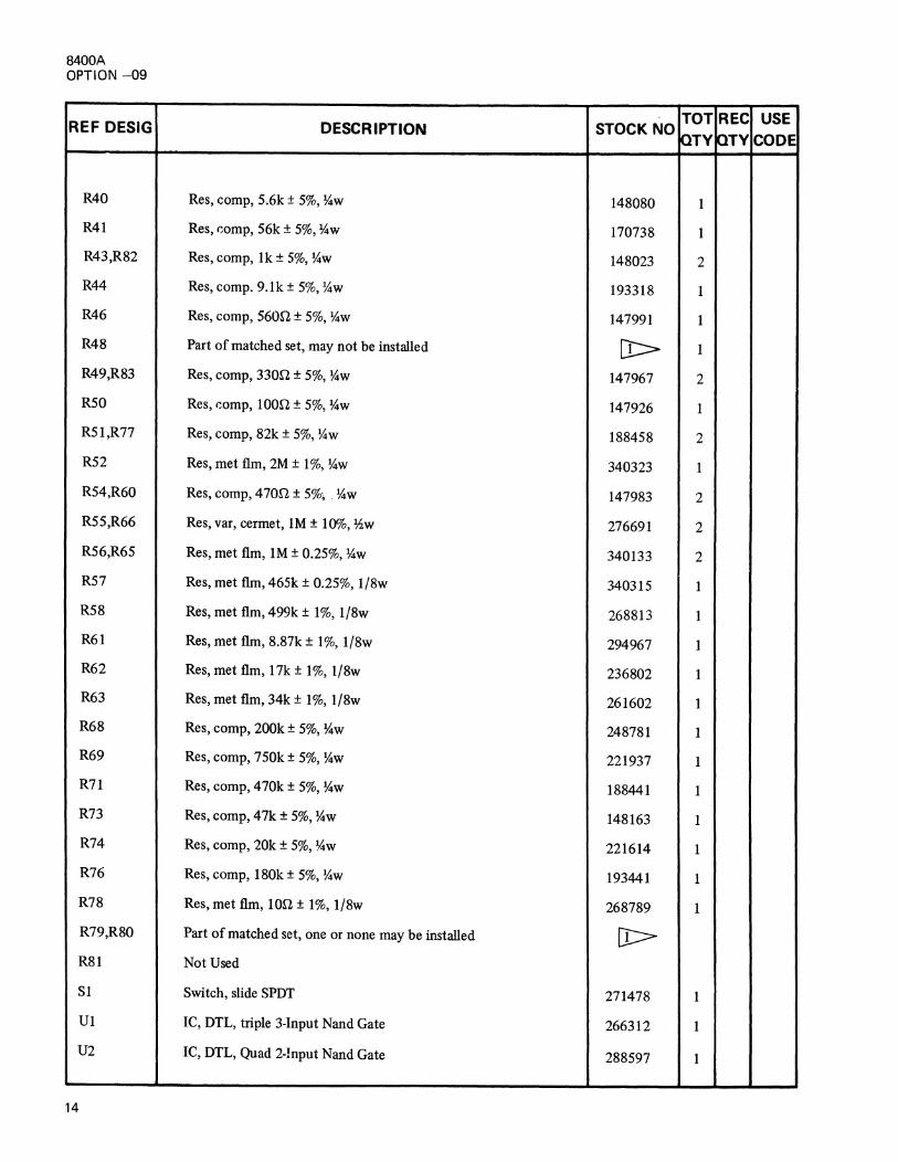
8400A OPTION -09
REF DESIG
R40
R4I
R43,R82
R44
R46
R48
R49,R83
RSO
R5I,R77
R52
R54,R60
R55,R66
R56,R65
R57
R58
R61
R62
R63
R68
R69
R71
R73
R74
R76
R78
R79,R80
R81
Sl
Ul
U2
14
DESCRIPTION
Res, comp, 5.6k ± 5%, %w
Res, r,omp, 56k ± 5%, %w
Res, comp, Ik ± 5%, %w
Res, comp. 9.Ik ± 5%, %w
Res, comp, 560Q ± 5%, %w
Part of matched set, may not be installed
Res, comp, 330Q ± 5%, %w
Res, r,omp, I OOQ ± 5%, %w
Res, comp, 82k ± 5%, %w
Res, met flm, 2M ± I%, %w
Res, comp, 470Q ± 5%~ . %w
Res, var, cermet, IM± IO%, *-w
Res, met flm, IM ± 0.25%, %w
Res, met flm, 465k ± 0.25%, 1/8w
Res, met flm, 499k ± I%, I/8w
Res, met flm, 8.87k ± 1%, 1/8w
Res, met flm, 17k ± 1 %, l/8w
Res, met flm, 34k ± 1%, 1/8w
Res, comp, 200k ± 5%, %w
Res, comp, 750k ± 5%, %w
Res, comp, 4 70k ± 5%, %w
Res, comp, 47k ± 5%, %w
Res, comp, 20k ± 5%, %w
Res, comp, 180k ± 5%, %w
Res, met flm, ton± 1%, 1/8w
Part of matched set, one or none may be installed
Not Used
Switch, slide SPDT
IC, DTL, triple 3-Input Nand Gate
IC, DTL, Quad 2-!nput Nand Gate
STOCK NO TOT REC USE QTY QTY CODE
I48080 I
I70738 I
I48023 2
I933I8 I
I4799I I
[l> I
I47967 2
I47926 I
I88458 2
340323 I
I47983 2
27669I 2
340I33 2
340315 I
268813 1
294967 1
236802 1
261602 1
248781 1
221937 I
188441 1
148I63 1
221614 1
193441 1
268789 1
D>-
271478 1
266312 1
288597 1
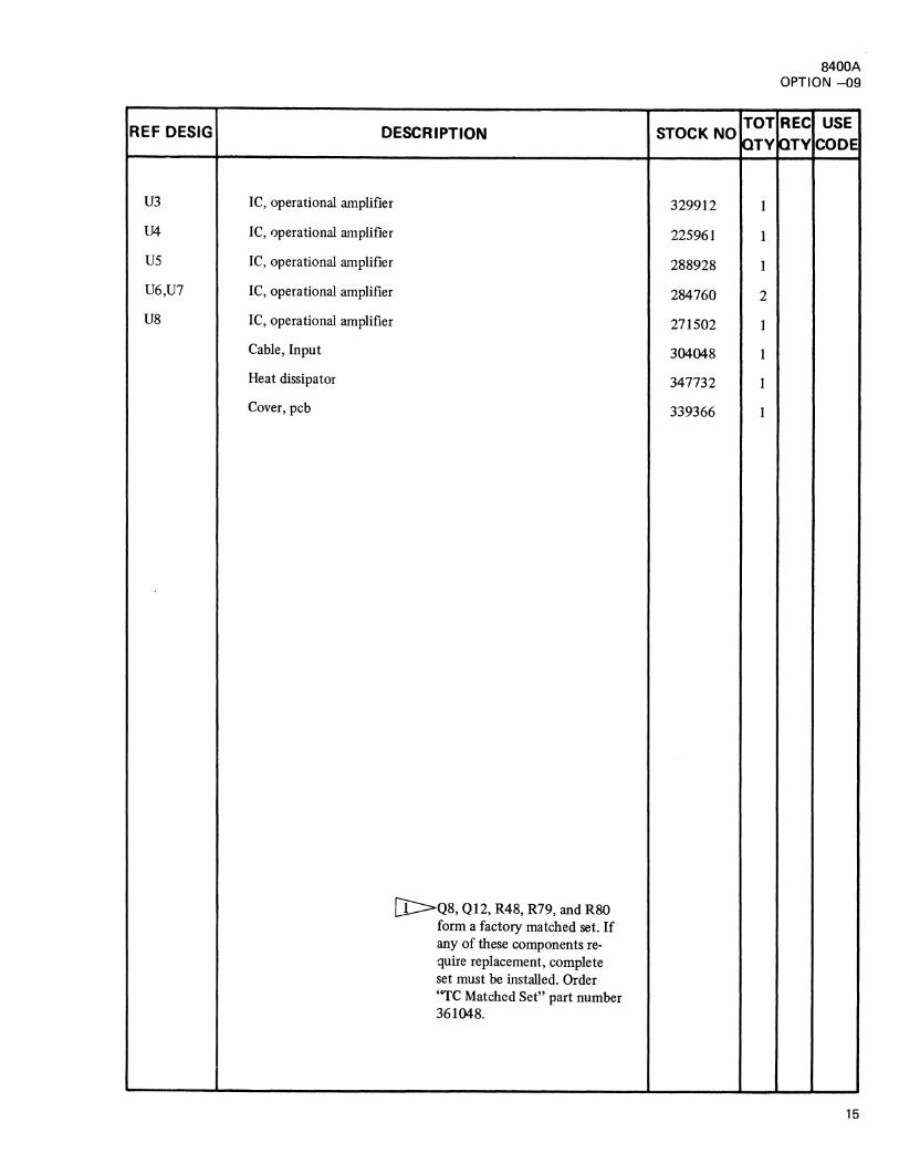
REF DESIG DESCRIPTION
U3 IC, operational amplifier
U4 IC, operational amplifier
us IC, operational amplifier
U6,U7 IC, operational amplifier
U8 IC, operational amplifier
Cable, Input
Heat dissipator
Cover, pcb
[l:::>Q8, Ql2, R48, R79, and R80 form a factory matched set. If any of these components re-quire replacement, complete set must be installed. Order "TC Matched Set" part number 361048.
STOCK NO
329912
225961
288928
284760
271502
304048
347732
339366
TOT
laTY
1
1
1
2
1
1
1
1
8400A OPTION -09
REC USE
laTY CODE
15

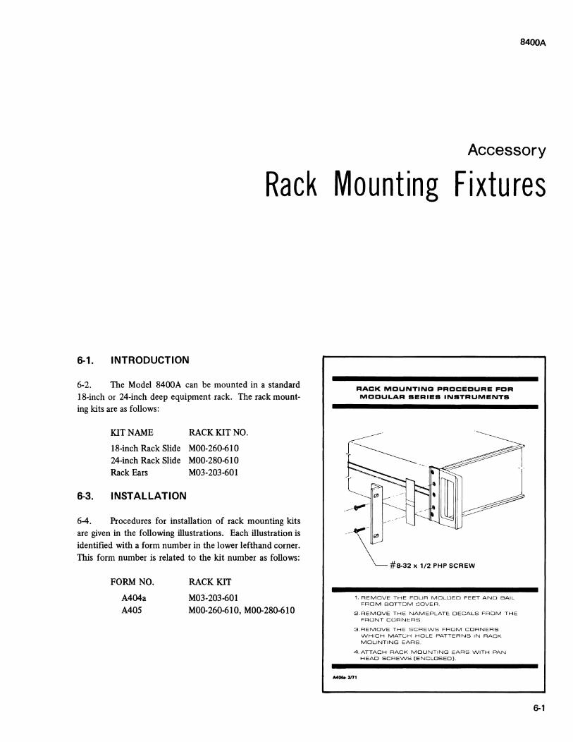
8400A
Accessory
Rack Mounting Fixtures
6-1. INTRODUCTION
6-2. The Model 8400A can be mounted in a standard 18-inch or 24-inch deep equipment rack. The rack mounting kits are as follows:
KIT NAME RACK KIT NO.
18-inch Rack Slide M00-260-610 24-inch Rack Slide M00-280-610 Rack Ears M03-203-601
6-3. INSTALLATION
6-4. Procedures for installation of rack mounting kits are given in the following illustrations. Each illustration is identified with a form number in the lower lefthand corner. This form number is related to the kit number as follows:
FORM NO.
A404a A405
RACK KIT
M03-203-601 M00-260-610, M00-280-610
RACK MOUNTING PROCEDURE FDR MODULAR SERIES INSTRUMENTS
__.,,-
~ #8-32 • "2 PHP SCREW
1. REMOVE THE FOUR MOLl~ED FEET ANO BAIL FROM BOTTOM COVER.
2.REMOVE THE NAMEPLATE DECALS FROM THE FRONT CORNERS.
3.REMDVE THE SCREWS FROM CORNERS WHICH MATCH HOLE PATTERNS IN RACK
MOUNTING EARS.
4. ATTACH RACK MOUNTING EARS WITH PAN HEAD SCREWS [ENCLOSED).
6-1

8400A
6-2
CHASSIS SECTION (B)
CENTER SECTION (C) ~ CABINET SECTION (D) __/
'O
~ #8-2 x 1/2" BIND. HD SCREW (A)
1. REMOVE SIDE TRIM DECAL AND BOTTOM FEET FROM INSTRUMENT. 3. INSTALL CABINET SECTION ID) AND CENTER SECTION IC) OF SLIDE INTO RACK !EXTENSION ANGLE BRACKET AND HARDWARE ENCLOSED).
2. ATTACH CHASSIS SECTION IB) OF SLIDE TO INSTRUMENT WITH # 8-32 x 1/2" PHP SCREWS IAI I ENCLOSED) AS FOLLOWS: 4. EXTEND CENTER SECTION IC) OF SLIDE TOWARD OPERATOR UNTIL IT
LOCKS IN EXTENDED POSITION. A. FOR 3-1/2", 7" AND 10-1/2" HIGH INSTRUMENTS UTILIZE
THE CENTER ROW MOUNTING HOLES. 5. DEPRESS SPRING LOCK ON CHASSIS SECTION IBI AND INSERT
B. FOR 5-1/4" AND 8-3/4" HIGH INSTRUMENTS UTILIZE EITHER THE UPPER OR LOWER ROW OF MOUNTING HOLES.
Fonn No. A406-3/71· Rew. 1
INSTRUMENT BETWEEN EXTENDED SLIDE SECTIONS.

8400A
Accessory
DOU, RCU Mating Connector
6-1. INTRODUCTION
6-2. The mating connector shown in Figure 6-1 is re
quired for interface between the Remote Control Unit and
the programming equipment. It also provides interface
between Data Output Unit No. I & 2 and external equip
ment. This connector is obtained when either option is
ordered, or can be obtained by ordering from the factory,
referencing FLUKE PART NO. 321687.
6-3. ASSEMBLY INSTRUCTIONS
6-4. Wiring and assembly of the mating connector is
done as follows:
a. Solder the wiring to the appropriate terminals of
the connector. Refer to Figure 6-1, detail I for
terminal locations. Functional pin assignments for
b.
c.
the Remote Control Unit and the Data Output
Unit No. I & 2 can be found in Section 2.
Mount alignment spacers (F) between proper pins
on Connector (B). Spacer positions are given in
Figure 6-2.
Mount Connector (B) into Backshell half (C). Refer
to detail II of Figure 6-1.
d. Mount Backshell half (A) onto Backshell half (C).
e.
f.
When correctly mounted together, the Backshell
halves snap in place.
Secure Backshell halfs (A) and (C) together with
4 screws (D), supplied.
Secure Connector (B) to Backshell halfs (A) and
(C) with two screws (E), supplied.
6-1

8400A
6-2
TAB ON BACKSHELL HALF (A} FITS HERE
0 =
DETAIL II
~ ~~Jlt g~~=~~! ,.~::~,. 17--::-1s i•-- .. --20 21 ----:;:;: : : ::::::-- 22 23 ":::/;/;. :: ~ 24
~!@Y~~!l 35-::!! ~ 36
DETAIL I
REAR VIEW
Figure 6-1.
RCU MATING CONNECTOR
~ 35{~36
2~4 I I 21 L22
FRONT VIEW
Figure 6-2.
TAB ON BACK.SHELL HALF (A) FITS HERE
DOU, RCU MATING CONNECTOR
DOU NO. 1 DOU NO. 2 MATING MATING CONNECTOR CONNECTOR
~ ~ "~" lll:
25 26
7~8 5 6
1 2
FRONT VIEW FRONT VIEW
ALIGNMENT SPACER POSITIONS

8400A
Accessory
Rear Input Mating Connector
6-1. INTRODUCTION
6-2. The mating connector shown in Figure 6-1 is required for interface between the rear panel INPUT connector and external equipment. This connector is obtained when the Rear Input Option (-07) is ordered, or can be obtained from the factory by referencing FLUKE PART NO. 321661.
6-3. ASSEMBLY INSTRUCTIONS
6-4. Wiring and assembly of the mating connector is
done as follows:
c:::::> c:::::;)
c:::> C:=l
,J ~ E
c
a.
b.
c.
d.
Solder wiring to connector pins (B).
Insert connector pins (B) into Connector (A). Refer to Figure 6-1 for terminal locations. Refer to the rear panel decal for functional pin assignments.
Mount and secure Cable Clamps (C) onto Connector (A) with proper hardware (D).
Secure Cable Clamps (C) together with screws (E).
05 90
04 0
03 A 70
02 0
01
---~ 1. SPARE 6. SPARE 2. GUARD 7. Q SOURCE LOW 3. INPUT LOW 8. SPARE 4. SPARE 9. Q SOURCE HIGH 5. INPUT HIGH
Figure 6-1. REAR INPUT MATING CONNECTOR
10/18/74 6-1


Exte rna I Reference
6-1. INTRODUCTION
6-2. The mating connector shown in Figure 6-1 is required for interface between the DC and AC External Reference connector and the external equipment. This
connector is obtained when either option is ordered, or can
be obtained by ordering from the factory by referencing FLUKE PART NO. 321679.
6-3. ASSEMBLY INSTRUCTIONS
6-4. Wiring and assembly of the mating connector is done as follows:
-B-~- -~
)
J
B
a.
b.
c.
d.
8400A
Accessory
Mating Connector
Solder the wiring to Terminals (B).
Insert Terminals (B) in Connector (A). Refer to Figure 6-I for terminal locations. Rear panel decal on instrument shows pin connections from External Reference Assembly to Connector.
Mount Cable Clamps (C) onto Connector (A) and secure with hardware (D) to Connector (A).
Secure both halfs of Cable Clamp (C) together with screws (E).
D
1 guard 2 -3 HI 4 LOW 5 -
FRONT VIEW
DETAIL I
Figure 6-1. EXTERNAL REFERENCE MATING CONNECTOR
10/18/74 6-1


6-1. INTRODUCTION
6-2. The Extender Card shown in Figure 6-1 is available as an Accessory for the FLUKE 8400A digital voltmeter. This accessory permits the printed circuit boards in the Model 8400A to be extended for servicing. The Extender Card can be obtained by ordering it under FLUKE PART NO. 298265 .
6-3. INSTALLATION
6-4. To install a printed circuit board on the Extender Card proceed as follows :
a. Disconnect 8400A from line power.
b. Remove top dust and guard covers from instrument.
c. Locate the printed circuit board to be serviced and remove it from the instrument.
d. Install the Extender Card into the connector vacated by the removal of the printed circuit board.
e.
f.
8400A
Accessory
Extender Card
Install the printed circuit board into the connector on the Extender Card. The printed circuit board must face the same direction as it did when installed into the instrument.
Connect 8400A to line power and turn on instrument. The printed circuit board can now be serviced.
Figure6-1. EXTENDER CARD
6-1


A90
ACCESSORY INFORMATION
MODEL A90 CURRENT SHUNT
6-1. INTRODUCTION
6-2. The Model A90 Current Shunt is designed for use with any high-impedance ac or de voltmeter capable of accurately measuring 100 millivolts. Six Fluke precision wire wound and strip resistors provide a 100 millivolt fullscale output for each of six pushbutton current ranges: 0.1, 1, 10, 100, and 1000 milliamperes and 10 amperes
(ac or de). Basic accuracy is specified over a frequency range of de to 4 kHz for the 10 ampere range and de to 10 kHz for the milliampere ranges .
6-3. The instrument is supplied in half-rack case so that it may be conveniently mounted side-by-side with other half-rack instruments in a standard 19-inch rack. A carrying handle detents into custom non-marring feet and serves as a tilt-up bail for bench use.
Figure 6-1. MODEL A90 CURRENT SHUNT
6-1

A90
Table 6-1. ACCURACY OF A90 (1year,15°C · 35°C)
RATED E SHUNT "OUTPUT" "OUTPUT" ACCURACY AS
CURRENT BURDEN R AT RATED % OF CURRENT INPUT
RANGE (APPROX.) CURRENT DC ONLY DC TO 10 KHZ AC
0.1 ma 100mv 1kn 100mv ±0.1% ±0.1%
* 0.1 ma 100mv 1 kn 100 mv +o.0% +o.0% --0.2% -0.2%
1.0 ma 100mv 1000 100mv ±0.1% ±0.1%
10 ma 100mv 1on 100mv ±0.1% ±0.1%
100ma 102mv 1n 100mv ±0.1% ±0.1%
1A 120mv o.1n 100mv ±0.1% ±0.2%
10A 300mv o.01n 100mv ±0.2% ±0.3% (to 4 kHz)
*With 1 Mn Input R Voltmeter. When Input R is ;;;i.10 Mn, use non-asterisked 0.1 ma specification.
A90 "INPUT" Posts A90 "OUTPUT" Posts
"BURDEN" I 0 SHUNT R I "OUTPUT"
Simplified diagram illustrating terms used in table.
6-4. SPECIFICATIONS
6-5. Electrical
RANGE
0.1, 1, 10, 100,and lOOOmilliamps and lOamperes.
ACCURACY Table 6-1 gives accuracy specifications for the Model A90 only. Total current measurement accuracy is also dependent
on the accuracy and input impedance of the voltmeter being used.
SENSITIVITY 100 millivolts full scale.
OVERLOAD Model A90 will not be damaged by 100% overload on each range below 10 amperes or by 50% overload on the 10 ampere range.
6-2
6-6. Mechanical
CURRENT SELECTION Pushbutton, each range.
CONNECTORS Positive ( +) and negative (-) INPUT and OUTPUT binding posts with separate input posts for 10 ampere range.
DIMENSIONS The Model A90 outline drawing is shown in Figure 6-2.
RACK MOUNTING KITS (OPTIONAL) MEE-7014: Side-by-side Half-rack Mounting Kit MEE-7006: Center Rack Mounting Kit MEE-7013: Left or right of center Mounting Kit.
6-7. AUXILIARY ELECTRICAL SPECIFICATIONS
6-8. Tables 6-2 through 6-6 provide accuracy specifications for the Model A90 when used with Fluke Models

TOP VIEW
FRONT VIEW
SIDE VIEW
Figure 6-2. MODEL A90 OUTLINE DRAWING
A 5.70
/
Table 6-2. A90/8100A ACCURACY. 30 days, @ 23°C ±5oc.
DC ACCURACY
CURRENT RANGE SPECIFICATION
0.1 ma ±(0.12% of current input + 0.1 ua)
1.0 ma ±(0.12% of current input+ 1.0 ua)
10ma .±(0.12% of current input + 10 ua)
100 ma ±(0.12% of current input+ 0.1 ma)
1A ±(0.12% of current input+ 1.0 ma)
10A ±(0.22% of current input + 10 ma)
AC ACCURACY
CURRENT RANGE 30 Hz - 50 Hz 50 Hz - 10 kHz
0.1 ma +(0.5% of current input+ 1.0 ua) +(0.2% of current input + 0.5 ua) -(0. 7% of current input + 1.0 ua) -(0.4% of current input + 0.5 ua)
1.0 ma ±(0.6% of current input+ 10 ua) ±(0.3% of current input+ 5.0 ua)
10ma ±(0.6% of current input+ 0.1 ma) ±(0.3% of current input+ 50 ua)
100 ma ±(0.6% of current input+ 1.0 ma) ±(0.3% of current input+ 0.5 ma)
1A ±(0. 7% of current input + 10 ma) ±(0.4% of current input + 5.0 ma)
10A ±(0.8% of current input + 100 ma) ±(0.5% of current input+ 50 ma) *
* 10A specified to 4 kHz only.
For: DC CURRENT AC CURRENT
Vr = 1v Vr = 1v
Vdfs = ±.1000 Vdfs = .1000
A90
6-3
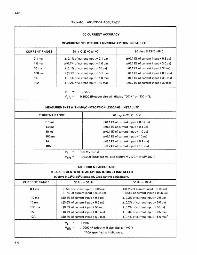
A90
Table 6-3. A90/8300A ACCURACY
DC CURRENT ACCURACY
MEASUREMENTS WITHOUT MV/OHMS OPTION INSTALLED
CURRENT RANGE 24 hr@23°c±1oc 90 days @ 23°C ±5°c
0.1 ma ±(0.1% of current input+ 0.1 ua) ±(0.11% of current input + 0.3 ua)
1.0ma ±(0.1 % of current input+ 1.0 ua) ±(0.11% of current input+ 3.0 ua)
10ma ±(0.1% of current input+ 10 ua) ±(0.11% of current input+ 30 ua)
100ma ±(0.1 % of current input+ 0.1 ma) ±(0.11% of current input+ 0.3 ma)
1A ±(0.1% of current input+ 1.0 ma) ±(0.11% of current input+ 3.0 ma)
10A ±(0.2% of current input+ 10 ma) ±(0.21% of current input+ 30 ma)
Vr = 10VDC
Vdfs = 0.1000 (Readout also will display "DC+" or "DC-").
MEASUREMENTS WITH MV/OHMSOPTION (8300A·02) INSTALLED
CURRENT RANGE 90 days @ 23°c ±5oc
0.1 ma ±(0.11% of current input+ 0.01 ua)
1.0ma ±(0.11 % of current input+ 0.1 ua)
10ma ±(0.11% of current input+ 1.0 ua)
100ma ±(0.11% of current input+ 10 ua)
1A ±(0.11% of current input+ 0.1 ma)
10A ±(0.21% of current input+ 1.0 ma)
Vr = 100 MV (0.1v)
Vdfs = 100.000 (Readout will also display MV DC+ or MV DC-)
AC CURRENT ACCURACY
MEASUREMENTS WITH AC OPTION 8300A-01 INSTALLED
90 days@ 23°C ±5°C using AC Zero control periodically.
CURRENT RANGE 30 Hz - 50 Hz 50 Hz -10 kHz
0.1 ma +(0.5% of current input+ 0.05 ua) +(0.1% of current input+ 0.05 ua) -(0.7% of current input+ 0.05 ua) -(0.3% of current input+ 0.05 ua)
1.0ma ±(0.6% of current input+ 0.5 ua) ±(0.2% of current input+ 0.5 ua)
10ma ±(0.6% of current input+ 5.0 ua) ±(0.2% of current input + 5.0 ua)
100ma ±(0.6% of current input+ 50 ua) ±(0.2% of current input+ 50 ua)
1A ±(0.7% of current input+ 0.5 ma) ±(0.3% of current input + 0.5 ma)
10A ±(0.8% of current input+ 5.0 ma) ±(0.4% of current input+ 5.0 ma)*
Vr = 1 VAC
Vdfs = .10000 (Readout will also display "AC")
*10A specified to 4 kHz only.
6-4

A90
Table 6-4. A90/9500A SPECIFICATIONS
ACCURACY WHEN UNKNOWN CURRENT IS 20% OR MORE OF A90 CURRENT RANGE. (23°C±1°C)
CURRENT RANGE 20 Hz - 50 Hz 50 Hz - 10 kHz
0.1 ma +(0.3% of current input + 0.02 ua) +(0.05% of current input+ 0.015 ua) -(0.5% of current input+ 0.02 ua) -(0.25% of current input+ 0.015 ua)
1.0 ma ±(0.4% of current input+ 0.2 ua) ±(0.15% of current input+ 0.15 ua)
10ma ±(0.4% of current input+ 2.0 ua) ±(0.15% of current input+ 1.5 ua)
100 ma ±(0.4% of current input+ 20 ua) ±(0.15% of current input+ 15 ua)
lA ±(0.5% of current input+ 0.2 ma) ±(0.25% of current input+ 0.15 ma)
10A ±(0.6% of current input+ 2.0 ma) ±(0.35% of current input+ 1.5 ma)*
ACCURACY WHEN UNKNOWN CURRENT IS BETWEEN 10% AND 20% OF A90 CURRENT RANGE.
A90 INPUT % OF INPUT ABSOLUTE ACCURACY 20 Hz - 50 Hz @ 23°C ± 1°c FOR (%OF A90 CURRENT RANGE
CURRENT 0.1 ma RANGE) + - 1 ma -100 ma lA lOA
10-11% 0.53% 0.73% ± 0.63% ±0.73% ±0.83%
12-14% 0.50% 0.70% ± 0.60% ±0.70% ±0.80%
15-17% 0.47% 0.67% ± 0.57% ±0.67% ±0.77%
18-20% 0.44% 0.64% ± 0.54% ±0.64% ±0.74%
A90 INPUT % OF INPUT ABSOLUTE ACCURACY 50 Hz - 10 kHz @23°C±1°C FOR
(%OF A90 CURRENT RANGE
CURRENT 0.1 ma
RANGE) + - 1 ma - 100 ma lA lOA*
10-11% 0.23% 0.43% ±0.33% ±0.43% ±0.53%
12-14% 0.20% 0.40",{, ±0.30% ±0.40% ±0.50%
15-17% 0.17% 0.37% ±0.27% ±0.37% ±0.47%
18-20% 0.13% 0.33% ±0.23% ±0.33% ±0.43%
Vr = . lv
Vdfs = .10000
TC = 0.005% of current input/°C 20 Hz -50 Hz 0.004% of current input/°C 50 Hz - 10 kHz
* 1 QA is specified to 4 kHz only.
6-9. INSTALLATION 8100A, 8300A, 9500A, 891A, 893A, and 9318. Table 6-7 gives V r and V dfs for each of the voltmeters listed in the tables in addition to various other Fluke voltmeters, where
Yr and Vdfs
Voltage range to be used on the voltmeter Nominal voltmeter reading with full-scale current in A90 shunt.
6-10. There are three rack-mount kits available, at additional cost, for use with the Model A90. Kit MEE-7014 allows the Model A90 to be mounted side-by-side with another half-rack instrument in a standard 19-inch rack. Kit MEE-7006 supplies hardware necessary to mount the
6-5
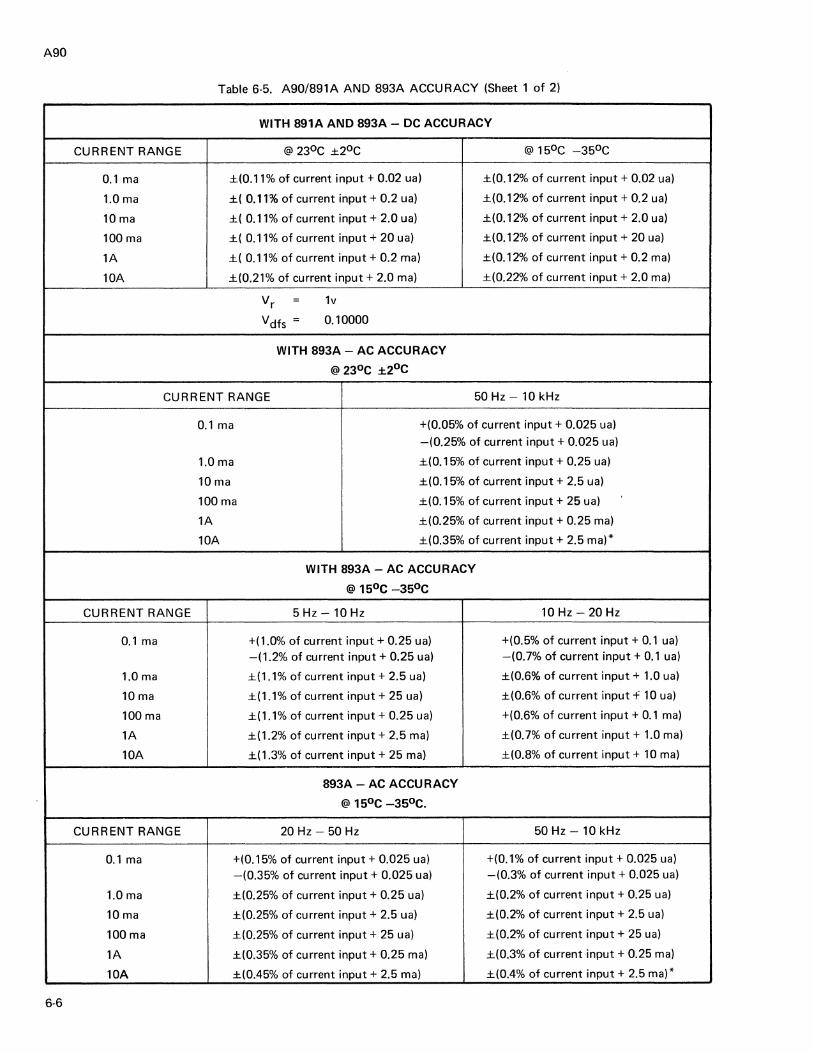
A90
Table 6-5. A90/891A AND 893A ACCURACY (Sheet 1 of 2)
WITH 891A AND 893A - DC ACCURACY
CURRENT RANGE @23oc ±2oc @ 15°c -35°c
0.1 ma ±(0.11% of current input+ 0.02 ua) ±(0.12% of current input+ 0.02 ua)
1.0ma ±( 0.11% of current input+ 0.2 ua) ±(0.12% of current input+ 0.2 ua)
10 ma ±( 0.11% of current input+ 2.0 ua) ±(0.12% of current input + 2.0 ua)
100 ma ±( 0.11% of current input+ 20 ua) ±(0.12% of current input+ 20 ua)
1A ±( 0.11% of current input+ 0.2 ma) ±(0.12% of current input+ 0.2 ma)
10A ±(0.21% of current input+ 2.0 ma) ±(0.22% of current input+ 2.0 ma)
vr = 1v
Vdfs = 0.10000
WITH 893A - AC ACCURACY
@23°c ±2°C
CURRENT RANGE 50 Hz - 10 kHz
0.1 ma +(0.05% of current input+ 0.025 ua)
-(0.25% of current input+ 0.025 ua)
1.0 ma ±(0.15% of current input+ 0.25 ua)
10 ma ±(0.15% of current input+ 2.5 ua)
100ma ±(0.15% of current input+ 25 ua)
1A ±(0.25% of current input+ 0.25 ma)
10A ±(0.35% of current input+ 2.5 ma)*
WITH 893A-AC ACCURACY
@ 15°C -35°C
CURRENT RANGE 5 Hz - 10 Hz 10Hz-20Hz
0.1 ma +( 1.0% of current input+ 0.25 ua) +(0.5% of current input+ 0.1 ua) -(1.2% of current input+ 0.25 ua) -(0. 7% of current input + 0.1 ua)
1.0ma ±(1.1% of current input+ 2.5 ua) ±(0.6% of current input+ 1.0 ua)
10 ma ±(1.1% of current input+ 25 ua) ±(0.6% of current input -f 10 ua)
100 ma ±(1.1% of current input+ 0.25 ua) +(0.6% of current input+ 0.1 ma)
1A ±(1.2% of current input+ 2.5 ma) ±(0.7% of current input+ 1.0 ma)
10A ±(1.3% of current input+ 25 ma) ±(0.8% of current input + 10 ma)
893A-AC ACCURACY
@ 15°c _35oc.
CURRENT RANGE 20 Hz - 50 Hz 50Hz-10kHz
0.1 ma +(0.15% of current input+ 0.025 ua) +(0.1% of current input+ 0.025 ua) -(0.35% of current input+ 0.025 ua) -{0.3% of current input + 0.025 ua)
1.0 ma ±(0.25% of current input+ 0.25 ua) ±(0.2% of current input+ 0.25 ua)
10ma ±(0.25% of current input+ 2.5 ua) ±(0.2% of current input+ 2.5 ua)
100ma ±(0.25% of current input+ 25 ua) ±(0.2% of current input+ 25 ua)
1A ±(0.35% of current input+ 0.25 ma) ±(0.3% of current input+ 0.25 ma)
10A ±(0.45% of current input+ 2.5 ma) ±(0.4% of current input+ 2.5 ma)*
6-6

A90
Table 6-5. A90/891A AND 893A ACCURACY (Sheet 2 of 2)
Vr 1v (AC or DC)
V dfs 0. 10000
* 1 OA is specified to 4 kHz only.
Table 6-6. A90/931B SPECIFICATIONS
ACCURACY WHEN UNKNOWN CURRENT IS 10% OR MORE OF A90 CURRENT RANGE
% OF INPUT ABSOLUTE ACCURACY SPECIFICATIONS CURRENT RANGE 2 Hz - 3 Hz 3 Hz - 5 Hz 5 Hz - 30 Hz 30 Hz - 10 kHz
0.1 ma +1.0% +0.5% +0.2% +(0.05% of current input+ 5 na) -1.2% -0.7% -0.4% -(0.25% of current input+ 5 na)
1.0 ma ±1.1% ±0.6% ±0.3% ±(0.15% of current input+ 50 na)
10 ma ±1.1% ±0.6% ±0.3% ±(0.15% of current input+ 0.5 ua)
100 ma ±1.1% ±0.6% ±0.3% ±(0.15% of current input+ 5 ua)
1A ±1.2% ±0.7% ±0.4% ±(0.25% of current input+ 50 ua)
10A ±1.3% ±0.8% ±0.5% ±(0.35% of current input+ 0.5 ma)*
TC= ±0.1%/°C ±0.05%/°C ±.0.025%/°C ±0.0025%/°C
vr = 100 MV
Vdfs = 100.000
*10A is specified to 4 kHz only.
Table 6-7. "Vr" AND "Vdfs" FOR VOLTMETERS OF TABLES 6-2 THROUGH 6-6
VOLTMETER "V r" "Vdfs"
8300A (Without MV /Ohms) 10v .010
8100A,871A,873A,881A,883A,885A,887A,891A,893A 1v .100
801,803,801B,803B,803D,821A,823A,825A 0.5v .100
9500A, 910A O. lv .100
8300A (With MV/Ohms), 931A, 9318 100 MV 100.0
vr = Voltage range to be used on the voltmeter.
Vdfs = Nominal voltmeter reading with full-scale current in A90 shunt.
instrument in the center of the rack. Kit MEE-7013 supplies two different sized rack ears so that the instrument can be mounted to the left or to the right of rack center.
6-11. OPERATING INSTRUCTIONS
6-12. A description of Model A90 controls and terminals is given in Figure 6-3.
6-13. Equipment Connections
6-14. It is recommended that the Model A90 always be used in the "LO" lead as shown in Figure 6-4A. When used in the "HI" lead, as shown in Figure 6-4B, the distributed capacitance, Cmsr. loads the source. When connected in the "HI" lead, the voltmeter guard should either be connected as shown or else the voltmeter should be battery operated.
6-7

A90
Figure 6-3. MODEL A90 CONTROLS AND TERMINALS.
6-15. At high ac currents, performance of the A90 may
depend upon the manner in which the current leads are connected to the input binding posts. Optimum performance is obtained when the input current leads are twisted.
6-16. Voltmeter Impedance
6-17 . The input impedance of the voltmeter which is used with the Model A90 is significant with regard to total measurement accuracy . As indicated in the specifications, Model A90 measurement accuracy is derated for voltmeters having finite input impedance. As the voltmeter input
capacity increases, the Model A90 response rolls off at the high end; and as the voltmeter input resistance decreases, the response shifts downward, resulting in negative measure
ment errors .
6-8
6-18. Combining Model A90 And Voltmeter Specifications
6-19 . Combined specifications for the A90 when used with various Fluke voltmeters is given in Tables 6-2 through 6-6 . When the A90 is used with other voltmeters, the following information may be used to combine specifications.
6-20 . Equation l (Figure 6-5) is used to combine A90 and voltmeter specifications for overall accuracy. The "W" term is taken from Table 6-1, and the "X", "Y" and "Z" terms are taken from voltmeter specifications (data sheets). All Fluke voltmeter specifications, except the Model 9 lOA, contain the "X" term ; they usually list the "Y" term and occasionally the "Z" term. Model 91 OA accuracy specifi-
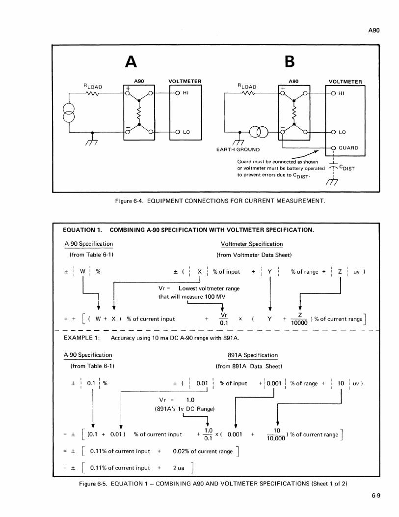
A B A90 VOLTMETER
EARTH GROUND ~~~~~-+---< I GUARD
~ Guard must be connected as shown
I _I_
or voltmeter must be battery operated "T' CDIST
to prevent errors due to CDIST· :
117
Figure 6-4. EQUIPMENT CONNECTIONS FOR CURRENT MEASUREMENT.
EQUATION 1- COMBINING A-90 SPECIFICATION WITH VOLTMETER SPECIFICATION.
A-90 Specification
(from Table 6-1)
I
±
~I
Voltmeter Specification
(from Voltmeter Data Sheet)
I I I
±( x % of input + I y I I I
% of range + 1 Z
~ J
Vr = Lowest voltmeter range
that will measure 100 MV
t
UV )
Vr + x
0.1 y + 1 O~OO ) % of current range J + [ ( W + X ) % of current input
A90
--- ---------!
EXAMPLE 1: Accuracy using 10 ma DC A-90 range with 891A.
A-90 Specification
(from Table 6-1)
±
±
I 0.1 I%
I
l [ (0.1 + 0.01 )
891 A Specification
(from 891 A Data Sheet)
± 0-01 : % of input + \ 0.001 i % of range + 10
J I r------'I J I J Vr 1.0
(891A's 1v DC Range)
% of current input
~ ~ + _!_:Q x ( 0.001
0.1
~
+ 10 ~000 ) % of current range J ± [ 0.11 % of current input +
± [ 0.11 % of current input +
0.02% of current range J 2 ua J
Figure 6-5. EQUATION 1 - COMBINING A90 AND VOLTMETER SPECIFICATIONS (Sheet 1of2)
UV)
6-9

A90
EXAMPLE 2: Accuracy using 0.1 ma AC A-90 range with 873A at 1 kHz.
Model 873A has 1 megohm input impedance in its AC mode so separate accuracy statements are required for
positive and negative limits of error for measurements made on the A-90's 0.1 ma range.
Positive Limit of Error
A-90 Specification 873A Specification
I I I I
+ 1 oj.o :
3 ·'" ... -----,,-v-r.-'-is_s_1_3_A_'_s ___ ±_~_o__.~c ;,~~ ;n~5 UV
' 1v AC Ronge ---i Jn Spec i + [ (0.0 + 0.2) % of cunonUnput + 0', , i+ . 10~ ) % of cumntrnngo:
+ [ 0.2% of current input + 0.025% of current range J Negative Limit of Error
[ (0.2 + 0.2) % of current input + 0.025% of current range J [ 0.4% of current input + 0.025% of current range. J
Figure 6-5. EQUATION 1 - COMBINING A90 AND VOLTMETER SPECIFICATIONS (Sheet 2 of 2)
cation consists of "Y" term only. If "X'', "Y", or "Z" do
not appear in a voltmeter accuracy specification, it should
be treated as a zero in Equation l. The voltmeter must be
used on the lowest range that can measure 100 millivolts.
This range is assigned the symbol "V r" in Equation 1. V r is always stated as volts, i.e., 100 millivolt range equals 0.1
volts for V r .
6-21. Equation 2 (Figure 6-6) may be used to convert
the voltmeter voltage reading to current.
6-22. THEORY OF OPERATION
6-23. The schematic diagram of the Model A90 is located at the back of the manual. In the milliampere ranges,
current is directed through the appropriate shunt resistor by switches SIA through SSA, and the corresponding output voltage is connected to the output terminals through
switches S 1 through SS, decks B and C. In 10 ampere range, the input current is applied directly to the shunt
resistor, and the output voltage is connected to the output
terminals through switch S6.
6-24. All shunt resistors are four-terminal shunts or are
connected in a four-terminal switching arrangement so that
lead resistance does not affect measurement accuracy.
6-10
6-25. MAINTENANCE
6-26. The following paragraphs contain instructions for
cleaning and calibrating the Model A90.
6-27. Cleaning
6-28. The instrument should be cleaned periodically to remove dust, grease, and other contamination. The following procedure should be adhered to when cleaning the
instrument:
a.
b.
Remove loose contamination with low-pressure,
clean, dry air.
Clean front panel and exterior surfaces with anhydrous ethyl alcohol or a soft cloth dampened
in a mild solution of detergent and water.
CAUTION!
Do not use aromatic hydrocarbons or chlorinated solvents on the front panel, because they will react with the Lexan binding posts.

Ix Ir x vd
Vdfs
A90
Where: Ix magnitude of unknown current in units of A90 "RANGE" used. (i.e. ma or amps).
Ir A90 Rated Current "RANGE".
vd Voltmeter reading.
Vdfs = Nominal Voltmeter reading with rated current flowing in A90. "V dts" and "Vr" are tabulated in Table 6-7 for each voltmeter listed in Tables 6-2 through 6-6. Note that
"V dts" multiplies or divides "V d" by powers of 10 so it is simple to manipulate.
EQUATION 2. CONVERTING VOLTAGE READINGS TO CURRENT
r-----------------------------Example: An 81 DOA reads =.0643 when used with an A90 in the 10 ma range. What current is flowing?
Answer:
10 ma (A90 "Rated Current Range")
.0643 (Voltmeter reading)
.1000 (From Table 6-7)
.0643 10 max .1000 6.43 ma
Figure 6-6. Equation 2 - CONVERTING VOLTAGE READINGS TO CURRENT
6-29. Test Equipment
6-30. Test equipment required for calibration and testing of the Model A90 is shown in Table 6-8. If the recommended equipment is not available, other equivalent equipment may be used.
Table 6-8. LIST OF TEST EQUIPMENT
NAME RECOMMENDED EQUIPMENT
Constant Current Fluke Model 382A
Source
DC Differential Fluke Model 895A or 885A
Voltmeter
Low-Thermal
Leads
4-Terminal Fluke Model 8300A with
Ohmmeter Option -02
6-31. Calibration
6-32. PRELIMINARY CHECKS. Make the resistance checks shown in Table 6-9. Values are approximate since check is intended to show only gross errors, such as defective or open resistors.
6-33. .1 MA AND 1 MA RANGE CHECKS. Connect the ohmmeter and A90, as shown in Figure 6-7, for 4-terminal resistance measurements, and perform the following steps:
a. Set the A90 to the .1 MA range. The ohmmeter should indicate between 1.00050 and 0.99950 kilohms. If the measured resistance is not within these limits, the .1 MA shunt, R6, is defective and must be replaced.
b. Set the A90 to the 1 MA range. The ohmmeter
should indicate between 100.07 and 99.93 ohms. If the measured resistance is not within these limits, the 1 MA shunt, RS, is defective and must be replaced.
6-34. lOMA, lOOMA,AND lOOOMA RANGE CHECKS. Connect the constant current generator, differential voltmeter, and A90 as shown in Figure 6-8 and perform the
following steps:
a. Set the A90 to the 10 MA range.
b. Set the differential voltmeter controls as follows: RANGE 1 Volt NULL Sensitivity 100 µV Readout Dials 0.100000
6-11
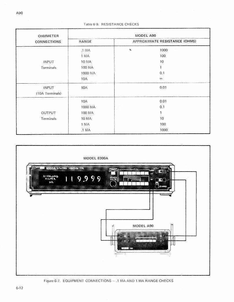
A90
Tab le 6-9. RESISTANCE CHECKS
OHMMETER MODEL A90
CONNECTIONS RANGE APPROXIMATE RESISTANCE (OHMS)
.1 MA " 1000
1 MA 100
INPUT 10 MA 10
Terminals 100 MA 1
1000 MA 0.1
10A cc
INPUT 10A 0.01
(10A Terminals) -
10A 0.01
1000 MA 0.1
OUTPUT 100 MA 1
Terminals 10 MA 10
1 MA 100
.1 MA 1000
MODEL 8300A
MODEL A90
Figure 6-7. EQUIPMENT CONNECTIONS - .1 MA AND 1 MA RANGE CHECKS
6-12

A90
MODEL 382A
:ti.I • ~- -~ .. ~, .• 0
0
I ·-::---@~- ······"··· ... ,.:\ 111/--.. -· .o ... , • • ,.. r'" .. i .. OJ 8 0 :::-::-·· . . t1... ..... _J &L22E@ •. J '--- _ _...A.,,-++-1--1
LOW-THERMAL LEADS
MODEL A90
MODEL 895A OR 885A
•:T 2 3 41!;
••••••
Figure 6-8. EQUIPMENT CONNECTIONS - 10 MA, 100 MA, AND 1000 MA RANGE CHECKS
c.
d.
Set the constant current generator for 10.0000
milliamperes output. The differential voltmeter
should indicate null within ±80 micorvolts. If
the voltmeter does not indicate within these limits,
the I 0 MA shun t , R4 , is defective and must be
replaced.
Change the A90 range to l 00 MA and the constant
current generator output to I 00 milliamperes. The
differential voltmeter should indicate null within
±80 microvolts. If the voltmeter does not in
dicate within these limits , the 100 MA shunt, R3 ,
is defective and must be replaced.
e. Change the A90 range to I 000 MA and the
constant current generator ou tput to 1000 milli
amperes . The differential vo ltmeter should in
dicate null within ±80 microvolts . If the +80
microvolt limit is not met, the 1000 MA shunt , R2 ,
should be replaced. If the -80 microvolt limit is
6-35 .
not met, R2 is low in ohmic value and can be
trimmed to its desired value by carefully removing
a small amount of material from the edge of the
shunt using a whetstone.
10 AMPERE RANGE CHECK. Connect equip-
ment as shown in Figure 6-8, leaving the constant current
generator temporarily disconnected from the A90 , and per
form the following steps:
a. Set the differnetial voltmeter controls as follows:
RANGE l Volt
NULL Sensitivity 100 µV
Readout Dials 0.00000
The voltmeter should indicate less than ±4 micro
volts of thermal offset. If more than ±4 micro
volt s of offset is observed, check for cold solder
joints or possible thermal generators in the test
6-13

A90
b.
c.
6-14
setup. When thermal offset has been reduced to within ±4 microvolts, proceed to step (b ).
Connect the constant current generator to the I 0 AMP binding posts of the A90 and set the A90 to the IOA range.
Set the differential voltmeter controls as follows:
RANGE I Volt NULL Sensitivity 100 µV Readout Dials .020000
d. Set the constant current generator output to 2 amperes, The voltmeter should indicate nu!! within ±80 microvolts. If the +80 microvolt limit is not met, the IO ampere shunt; Rl, should be replaced. If the -80 microvolt lim.li is not met, Rl is low in ohmic value and can be trimmed to its desired value by carefully removing a small amount of material from the edge of the shunt using a whetstone.
6-36. LIST OF REPLACEABLE PARTS

A90
•-· - -r..-.... ~,.. ,.,...
REF INDEX DESCRIPTION
STOCK MFH TOT R-EC USE MFn
DESIG NO NO P/.lif.n NO QTY TY CODE ___ '. ____ _ ___ ,, r ....... , ... r·-··u ... ,..·-~--
CURRENT SHUNT - Figure 6-9 A90
Shunt PCB Assembly (See "'A.90403 8953 A90-403 Figure 6-9)
11 , 12, Binding post , red , + 275552 89536 275552 3 JS
13, 14 , Binding post, black - 275560 89536 275560 3 16
Cover, bottom 224360 89536 224360
Cover, top 224352 89536 224352
Foot 230037 89536 230337 4
Handle , carrying 231423 89536 231423
Panel, front A90-208 89536 A90-208
Panel, rear A90-209 89536 A90-209
J1 J2 A90-208 J5
Figure 6-9. MODEL A90 CURRENT SHUNT (Sheet 1 of 2)
6-15

A90
REF INDEX DESCRIPTION
STOCK MFR TOT REC USE
DESIG NO NO MFR
PART NO QTY TY CODE
SHUNT PCB ASSEMBLY - A90-403 895 36 A90-403 REF Figure 6-9 "
Rl Res, ww, 0.010.Q ±0.2%, l w 344022 89536 34-4022
R2 Res,ww,0 .10.Q±0.1%, lw 224121 89536 224121
R3 Res , ww, I.Ort ±0.1 %, Yzw 224089 89536 224089
R4 Res, ww, 10.Q ±0.1%, Yzw 224071 89536 224071
RS Res , ww, 100.Q ±0.03%, Yzw 155846 89536 155846
R6 Res, ww, 1 Kn ±0.04%, Yzw 131706 89536 131706
SI thru Switch assembly, RANGE MA A90-802 89536 A90-802 S6
R4
___ RS
A90- ___ _
403
---R1
~---- 231423
Figure 6-9. MODEL A90 CURRENT SHUNT (Sheet 2 of 2)
6-16
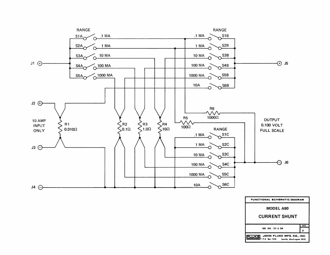
RANGE RANGE
S1A .1 MA .1 MA S1B
S2A 1 MA 1 MA 528
S3A 10 MA 10 MA 538
J1 0 S4A 100MA 100 MA 548 + J5
S5A 1000 MA 1000 MA 558
10A 568
J2 + R6
10AMP R5 1000.Q
OUTPUT
INPUT 100.Q 0.100 VOLT ONLY RANGE FULL SCALE
.1 MA S1C
J3 -1 MA S2C
10 MA S3C
100MA S4C - J6
1000 MA S5C
J4 -10A S6C
FUNCTIONAL SCHl!MATIC DIAGRAM
MODELA90
CURRENT SHUNT
511. NO. 121 & ON _G] lt=LUKEI JOHN FLUKE MFG. CO •• INC.
• P.0- loa 7421 Seattle, Washia9tH 91133

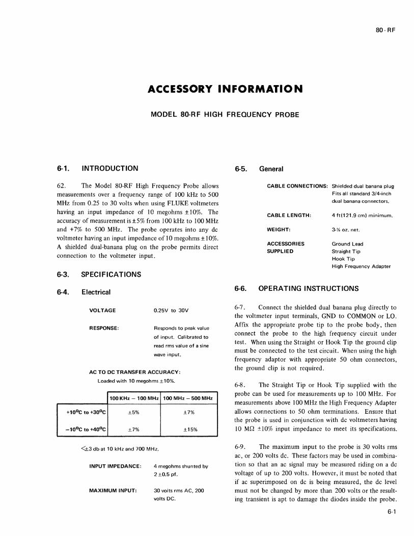
80-RF
ACCESSORY INFORMATION
MODEL 80-RF HIGH FREQUENCY PROBE
6-1. INTRODUCTION
62. The Model 80-RF High Frequency Probe allows measurements over a frequency range of 100 kHz to 500 MHz from 0.25 to 30 volts when using FLUKE voltmeters having an input impedance of 10 megohms ± 10%. The accuracy of measurement is ±5% from 100 kHz to I 00 MHz and +7% to 500 MHz. The probe operates into any de voltmeter having an input impedance of I 0 megohms± I 0%. A shielded dual-banana plug on the probe permits direct connection to the voltmeter input.
6-3. SPECIFICATIONS
6-4. Electrical
VOLTAGE
RESPONSE:
0.25V to 30V
Responds to peak value
of input. Calibrated to
read rms value of a sine
wave input.
AC TO DC TRANSFER ACCURACY:
Loaded with 10 megohms ±10%.
100 KHz - 100 MHz 100 MHz - 500 MHz
+1o0 c to +3o0 c ±5% ±7%
-1 o0 c to +4o0 c ±7% ±15%
<±.3 db at 10 kHz and 700 MHz.
INPUT IMPEDANCE:
MAXIMUM INPUT:
4 megohms shunted by
2±0.5 pf.
30 volts rms AC, 200
volts DC.
6-5. General
CABLE CONNECTIONS: Shielded dual banana plug
Fits all standard 3/4-inch
dual banana connectors.
CABLE LENGTH: 4 ft(121.9 cm) minimum.
WEIGHT: 3-Y. oz. net.
ACCESSORIES Ground Lead
SUPPLIED Straight Tip
Hook Tip
High Frequency Adapter
6-6. OPERATING INSTRUCTIONS
6-7. Connect the shielded dual banana plug directly to the voltmeter input terminals, GND to COMMON or LO. Affix the appropriate probe tip to the probe body, then connect the probe to the high frequency circuit under test. When using the Straight or Hook Tip the ground clip must be connected to the test circuit. When using the high frequency adaptor with appropriate 50 ohm connectors, the ground clip is not required.
6-8. The Straight Tip or Hook Tip supplied with the probe can be used for measurements up to 100 MHz. For measurements above 100 MHz the High Frequency Adapter allows connections to 50 ohm terminations. Ensure that the probe is used in conjunction with de voltmeters having 10 Mn ±10% input impedance to meet its specifications.
6-9. The maximum input to the probe is 30 volts rms ac, or 200 volts de. These factors may be used in combination so that an ac signal may be measured riding on a de voltage of up to 200 volts. However, it must be noted that if ac superimposed on de is being measured, the de level must not be changed by more than 200 volts or the resulting transient is apt to damage the diodes inside the probe.
6-1

80-RF
6-10. THEORY OF OPERATION
6-11. Figure 6-1 contains a schematic diagram of the probe. Cl is a de blocking capacitor, CRl is used as a detector, and Rl, R3, CR2, R2, and Rin form a divider network. C 1, charging through CRl during the negative half cycle of the input produces a positive de voltage at the CRl-Rl junction which equals the negative peak value of the input signal. The divider network reduces this to the rms value of the input. It can be seen that the probe must be operated into a 10 Mn load in order to maintain the proper division ratio.
6-12. CR2 provides compensation for the non-linearity of the detector. R3 is a selected part having a value of 50 kn to 100 kn, as required for proper divider action.
C1 100pf
R1 825K
R3 (selected)
I~ UT ) ---~vv,,-----1vv,,__. __ --i.
Figure 6-1. SCHEMATIC
AC SIGNAL SOURCE
I I
<~ Rjn ~> 10M I I
6-13. MAINTENANCE
6-14. Performance Checks
6-15. The following checks verify the probe AC to DC Transfer accuracy.
6-16. LOW FREQUENCY RESPONSE. Connect equipment as shown in Figure 6-2, and perform the following steps.
a. With equipment as shown in connection "A" adjust the ac signal source for an output of 3.000 volts rms at 100 kHz as measured on the DVM.
b. In connection "B" with the DVM set to measure de, observe a probe output of 3.15 to 2.85 volts.
c. Placing cables back in connection "A", decrease the ac signal source by lOdb (0.95 volts).
d. Moving back to connection "B", observe a voltmeter indication of between 1.00 and 0.90 volts (10 db down from 3 volts).
DVM
CONNECTION "A"
,~-tn::a-----------------j~ ----',' 50 OHM ,' t::J-FEED THRU ' l
-------m:c:i:.--<,., I '',, PROBE 80- RF l '---~·c CONNECTION .. ,.. fi---)
BNC ADAPTER
Figure 6-2. LOW FREQUENCY RESPONSE CHECK
6-2

' I
'
AC SIGNAL SOURCE DVM
POWER METER
80-RF
GENERAL RADIO TYPE 874
TO TYPE N FEMALE
GENERAL RADIO TYPE 874
TO TYPE N MALE
Figure 6-3. HIGH FREQUENCY RESPONSE CHECK
e.
f.
g.
h.
In connection "A", decrease the ac signal source an additional 10 db (to 0.3 volts) as indicated by the voltmeter in its ac function.
Back to "B", observe a voltmeter reading of .315 to .285 vdc.
Return the ac signal source back to 3_000 vrms.
Repeat steps a through g with frequencies of 500 kHz, 1 MHz, and 10 MHz.
6-17. HIGH FREQUENCY RESPONSE. Connect equipment to the 80-RF probe as shown in Figure 6-3, and perform the following steps:
a. Set the ac signal source ot 100 MHz with an output level of 10 milliwatts as indicated on the power meter. Ensure that the ac signal source has stabilized at 10 millivolts output.
b_ Observe that the voltmeter indication is between 0_757 and 0.657 volts. (0.707 volts corresponds to 10 milliwatts in 50 ohms).
c. Repeat the above for frequencies of 200 MHz, 300 MHz, 400 MHz, and 480 MHz.
6-18. Calibration
6-19. Should the 80-RF require recalibration, perform the following steps:
a.
b.
Perform steps a and b in paragraph 6-16, with a frequency of 1 MHz.
Observe the de voltmeter indication; a reading below 3 volts calls for a decrease in the value of R3, a reading above 3 volts calls for an increase in R3. Resistor R3 should be a 1/8 W metal film type. In a probe that is working properly, a 30 kn change in R3 will produce about a 1 % reading deviation.
6-20. Cleaning
6-21. The Model 80-RF requires a minimum amount of cleaning. Accumulation of dust or dirt particles between the output terminals of the Model 80-RF can be removed using clean dry pressurized air. Stubborn particles can be removed following an application of isopropyl alcohol.
6-3

REV.5 7189
Section 7
General Information
7-1. This section of the manual contains generalized user information as well as supplemental information to the List of Replaceable Parts contained in Section 5.
7-1

D9816 Westennann Wilhelm Augusla-Anlage Mannheim-Naclwau Gcnnany
S0482 Sony Corp. Tokyo, Japan·
S3774 Oshino Electric Lamp Worlcs Tokoyo, Japan
OAD86 INGcncnl El Paso, TX
OAE89 Autosplice Inc. Woodside, NY
OBW21 Norilake Co. Inc. Burlington, MA
OANFO Topaz Semiconductor Inc San Jose, CA
ODSM7 Conductive (Pkg) Conlainers Inc. Brookfield, WI
OCLN7 Emhart Fastening Group Shelton, CT
OPB81 S-Mos Systems Inc. San Jose, CA
OFF Pl Everready LTD Ever Ready Special Battery Div. Dawley Telford Salop UK
00199 Mareon Electronics Corp Kearny, NJ
00213 N ytronics Comp. Group Inc. Darrlingon, NC
00327 Welwyn International Inc. Westlake, OH
00656 Aerovox Corp. New Bedford, MA
00686 Film Capacitors Inc. Passaic, NJ
00779 AMP, Inc. Harrisburg, Pennsylvania
00853 Sangamo Weston Inc Components Div Pickens, NC
01091 Allied Plastics Co. Los Angeles, CA
7-2
Federal Supply Codes for Manufacturers
01101 fYlUJ1 Wabash Inc Paiker-Hannifin Corp. (Formerly Wabash Magnetics) 0-RingDiv Wabash, IN Lexington, KY
01121 02735 Allen Bradley Co. RCA-Solid S1ate Div. Milwaukee, WI Somerville, NJ
01281 ' TRW Electtonics & Defense Sector 02768 RF Devices ITW (IL Tool Wodts) Lawndale, CA Fastex Division
Des Plaines, IL 01295 TX Instruments Inc. 02799 Semiconductor Group Areo Electronics Inc. Dallas, TX Chatswonh, CA
01526 03296 Genicom Nylon Molding Corp. Waynesboro, VA Monrovia, CA
01537 03445 MOlorola Communications & Lercon Electronics Inc Elcc1ronics Inc. Burbank, CA Franklin Park, IL
03508 01686 Genenl Electric Co. RCL Electronics/Shallcross Inc. Semiconductor ProduCIS Electro Components Div. &Baneries Manchester, NH Auburn, NY
01884 03797 Sprague Electric Co. Genisco Technology Corp. (Now56289) E11ronics Div.
Rancho Dominquez, CA 01961 Varian Associates Inc. 03877 Pulse Engineering Div. Gilbett Engineering Co.Inc Convoy, CT Incon Sub ofTransitron
Electronic Corp. 01963 Glendale, AZ Cherry Electrical Products Corp Waukegan, IL 03888
KDI Electronics Inc. 02111 Pyrofilm Div. Spectrol Electronics Corp. Whippany, NJ City oflndustry, CA
03911 02114 Clairex Corp. Ampcrex Electronic Corp. Claircx Electronics Div. Ferrox Cube Div. Mount Vernon, NY Saugerties, NY
03980 02131 Muirhead Inc. General Instrument Corp. Mounlainside, NJ Government Systems Div. Westwood, MA 04009
Cooper Industries, Inc. 02395 Arrow Hart Div. Sonar Radio Corp. Hanford, CT Hollywood, l'L
04217 02533 Essex International Inc. Leigh Instruments Ltd. Wire & Cable Div. Frequency Control Div. Anaheim, CA Don Mills, Onlario, Canada
04221 02606 Midland-Ross Corp. FenwalLabs MidtcX Div. Division of Travenal Labs N. Mankato, MN Morton Grove, IL
04222 02660 AVXCorp. Bunker Ramo-Eltra Corp. A VX Ceramics Div. Amphenol NA Div. Myrtle Beach, SC Broadview, IL
04423 Tel.onic Berkley Inc. Laguna Beach, CA
04713 Motorola Inc. Semiconductor Group Phoenix, AZ
04946 S1andard Wire and Cable Rancho Dominquez, CA
05173 General Radio NY,NY. Replaced by:
24655 Genrad,INC. Concord, MA
05236 Jonathan Mfg. Co. Fullerton, CA
05245 Coreorn Inc. Libertyville, IL
05276 ITTPanona Electronics Div. Pomona, CA
05277 Westinghouse Elec. Corp. Semiconductor Div. Youngwood, PA
05347 Ultronix Inc Grand Junction, CO
05397 Union Carbide Corp. Materials Systems Div. Cleveland. OH
05571 Sprague Electric Co. (NowS6289)
05574 Viking Connectors Inc Sub of Criton Coip. Chatswonh, CA
05791 LYN-TRON Burbank, CA
05820 EG & G W akc:field Engineering Wakefield, MA
05839 Advance Elcctrical Chicago, IL
05972 Loctite Corp. Newington, CT

Federal Supply Codes for Manufacturers (cont}
06001 07047 08111 IB715 General Elcctric Co. Ross Milton Co., The MF Electronics (United Shoe & Nylock Corp) Electric Capacitor Product Southampton, PA New Rochelle, NY -Nylock Fastener Corp.-Section Paramus, NJ Columbia, SC 07138 08235
Westinghouse Electric Corp. lndustro Trans is tor Corp. 10059 06141 Industrial & Government Long Island City, NY Barker Engineering Corp. Fairchild Weston Systems Inc. Tube Div. Kenilworth, NJ Data Systems Div. Horseheads, NY 08261 Sarasota, FL Spectra-Strip 10389
07233 An Eltra Co. IL Tool Worl<s Inc. 06192 Benchmarl< Technology Inc. Garden Grove, CA Licon Div. La Deau Mfg. Co. City of Industry, CA Chicago, IL Glendale, CA 08445
07239 Electri-Cord Mfg., Inc 11236 06229 Biddle Instruments Westfield, PA CTS Corp. Electrovcrt Inc. Blue Bell, PA Resistor Products Div. Elmsford, NY 08530 Berne, IN
07256 Reliance Mica Corp. 06383 Silicon Transistor Corp. Brooklyn, NY 11237 Panduit Corp. Sub of BilF Inc. CTS Corp of CA Tinley Park, IL Chelmsford, MA 08718 Electro Mechanical Div.
!Tf Cannon Electric Paso Robles, CA 06473 07261 Phoenix Div. BWlker Ramo Corp. Avnet Corp. Phoenix, AZ 11295 Amphenol NA Div. Culver City, CA ECM Motor Co. SAMS Operation 08806 Schaumburg, IL Chatsworth, CA 07263 General Electric Co.
Fairchild Semiconductor Minature Lamp Products 11358 06540 North American Sales Cleveland, Oil Columbia Broadcasting System Mite Corp Ridgcview, CT CBS Electronic Div. Amatom-Electrical Div 08863 Newburyport, MA
07344 Nylomatic 06555 Bircher Co. Inc., The Fallsington, PA 11403 Beede Electrical Instrument Rochester, NY Vacuum Can Co. Penacoak, NH 08988 Ilest Coffee Maker Div.
07374 Skottie Electronics Inc. Chicago, IL 06665 Optron Corp Archbald, PA Precision Monolithics Woodbridge, CT 11502 (can also use 35009) Sub of Bourns Inc. 09021 TRW Inc. Santa Clara, CA 07557 Airco Inc. TRW Resistive Products Div.
Campion Co. Inc. Airco Electronics Boone, NC 06666 Philadelphia, PA Bradford, PA General Devices Co. Inc. 11503 INpolis,IN 07597 09023 Keystone Columbia Inc.
BumdyCorp. Comell-Dublier Electronics Freemon!, IN 06739 Tape/Cable Div. Fuquay-Varina, NC Electron Corp. Rochester, l\1Y 11532 Littleton, CO 09214 Teledyne Relays Teledyne
07716 General Electric Co. Industries Inc. 06743 TRW Inc. (Can use 11502) Semiconductor Products Dept. Hawthorne, CA Gould Inc. !RC Fixed Resistors/ Auburn, NY Foil Div. Burlington 11711 Eastlake, OH Burlington, VT 09353 General Instrument Corp.
C and K Components Inc. Rectifier Div. 06751 07792 Newton, MA Hicksville, NY Components Inc. Lerma Engineering Corp. SemcorDiv. Northampton, MA 09423 11726 Phoenix, AZ Scientific Components Inc. Qualidyne Corp.
07810 Santa Barbara, CA Santa Clara, CA 06776 Bock Corp. Robinson Nugent Inc. Madison, WI 09922 12014 New Albany, IN BumdyCorp. Chicago Rivet & Machine Co.
07910 Norwalk, CT Naperville, IL Teledyne Semiconductor
06915 Mtn. View, CA 09969 12020 Richco Plastic Co. Dale Electronics Inc. Ovenaire Chicago, IL 07933 Yankton, SD Div. of Electronic Technologies
Raytheon Co. Charlottesville, VA 06961 Semiconductor Div. 09975 Vernitron Corp. Mountain View, CA Burroughs Corp. 12038 Piezo Electric Div. Electronics Components Simco Bedford, OJI 08FG6 Detroit, MI (Div of Ransburg Corp)
Calmos Systems Inc. Hatfield, PA 06980 Kanata, Ont. Canada 1A791 EIMAC LFE Electronics 12040 (See Varian) 080A9 Danvers, MA National Semiconductor Corp. San Carlos, CA Dallas Semiconductor Danbury, CT
Dallas, TX
7-3

Federal Supply Codes for Manufacturers (cont)
12060 13050 14704 16473 Diodes Inc. Potter Co. Crydom Controls Cambridge Scientific Industries Nortluidge, CA Wesson, MS (Division of Int Rectifier) Div. of Chemed Corp.
El Segundo, CA Cambridge, MD 12136 13103 PHC Industries Inc. Thermalloy Co., Inc. 14752 16733 Formerly Philadelphia Handle Co. Dallas, TX Electro Cube Inc. Cablewave Systems Inc. Camden, NJ San Gabriel, CA North Haven, CT
13327 12300 Solitron Devices Inc. 14936 AMF Canada Ltd. Tappan, NY Genend Instrument Corp. 16742 Potter-Brumfield Discrete Semi Conductor Div. Paramount Plastics Guelph, Ontario, Canada 13511 Hicksville, NY FabricatOis Inc.
Bunker-Ramo Corp. Downey, CA 12323 Amphenol Cadre Div. 14949 Practical Automation Inc. Los Gatos, CA Trompeter Electronics 16758 Shelton, CT Chats worth, CA General MotOis Corp.
Delco Electronics Div. 12327 13606 15412 Kokomo, IN Freeway Corp. Sprague Electric Co. Amtron Cleveland, OH (Use56289) Midlothian, IL 17069
Circuit Structures Lab 12406 13689 15542 Burl>ank, CA Elpac Electronics Inc. SPS Technologies Inc. Scientific Components Corp. Santa Ana, CA Hatfield, NJ Mini -Circuits Laboratory Div. 17117
Brooklyn, NY Electronic Molding Corp. 13764 Woonsocket, RI
12443 Micro Plastics 15636 BuddCo.,The Flippin, AZ Elec-Trol Inc. 17338 Plastics Products Div. Saugus, CA High Pressure Eng. Co. Inc. Phoenixville, PA 13919 OK City, OK
BWT-Brown Research Corp. 15782 12581 Tucson, AZ Bausch & Lomb Inc. 17504 Hitachi Metals lnemational Ltd. Graphics & Control Div. Aluminum Filter Co. Hitachi Magna-Lock Div. 14099 Austin, TX Carpinteria, CA Big Rapids, MO Semtcch Corp.
Newbury Park, CA 15801 17545 12615 Fenwal Eletronics Inc. Atlantic SemiconductOis Inc. US Terminals Inc. 14140 Div. of Kidde Inc. Asbury Puk, NJ Cincinnati, OH McGray-Edison Co. Framingham, MA
Commercial Development Div. 17745 12617 Manchester, NH 15818 Angstrohm Precision, Inc. Hamlin Inc. Teledyne Inc. Co. Hagemown, MD LaKe Mills, WI 14189 Teledyne Semiconductor Div.
Ortronics, Inc. Mountain View, CA 17856 12673 Orlando, FL Siliconix Inc. Wesco Electrical 15849 Santa Clara, CA Greenfield, MA 14193 Usecoinc.
Cal-R-Inc. (Now88245) 18178 Santa Monica, CA E G & Gvactee Inc.
12697 15898 St. Louis, MO Clarostat Mfg. Co. Inc. 14301 International Business Dover, NH Anderson Electronics Machines Corp. 18235
Hollidaysburg, PA Essex Junction, VT KRL/Bantry Components Inc. 12749 Manchester, NH James Electronic Inc. 14329 16068 Chicago, IL Wells Electronics Inc. ln1emational Diode Div. 18310
South Bend, IN Harrison, NJ Concord Electronics 12856 New Y orlt, NY MicroMetals Inc. 14482 16162 Anaheim, CA Watkins-Johnson Co. MMI 18324
Palo Alto, CA Southfield, Ml Signetics Corp. 12881 Sacramento, CA MetexCorp. 14552 16245 Edison, NJ Microsemi Corp. Conaplnc.
(Formerly Micro-Semiconductor) Olean, NY 18377 12895 Santa Ana, CA Patlex Corp. Cleveland Electric Motor Co. 16258 Methuen, MA Cleveland, OH 14604 Space-Lok Inc.
Elm wood SensOIS, Inc Burl>ank,CA 18520 12954 Pawtucket, RI Sharp Electronics Corp. Microsemi Corp. 16352 Paialllus, NJ Components Group 14655 Codi Corp. Scottsdale, AZ ComcJl-Dublier Electronics Linden, NJ 18542
Div. of Federal Pacific Wabash Inc. 12969 Electric Co. Govt Cont Dept. 16469 Wabash Relay & Electronics Div. Unitrode Corp. Newaik,NJ MCLlnc. Wabash, IN Lexington, MA LaGrange, IL
7-4
18565 Chomerics Inc. Woburn, MA
18612 Vishay Intertechnology Inc. Vishay Resistor Products Group Malvern, PA
18632 Norton-Chemplast Santa Monica, CA
18677 Scanbe Mfg. Co. Div. of Zero Corp. El Monte, CA
18736 V oltronics Corp. East Hanover, NJ
18786 Micro-Power Long Island City, NY
18927 GTE Products Corp. Precision Material Products Business Parts Div. Titusville,P A
19080 Robinson Electronics Inc. San Luis Obispo, CA
19112 GanyCorp. Langhorne, PA
19315 Bendix Corp., The Navigation & Control Group Terboro,NJ
19451 Perine Machine Tool Corp. Kent, WA
19482 Delta Electronics Alexandria, VA
19613 MN Mining & Mfg. Co. Textool Products Dept. Electronic Product Div. Irving, TX
19647 Caddock Electronics Inc. Riverside, CA
19701 Mepco/Centralab Inc. A N. American Philips Co. Mineral Wells, TX
2B178 Wire Products Cleveland, OH
2K262 Boyd Corporation Portland, OR
Federal Supply Codes for Manufacturers (cont)
2Y384 North American Philips Lighting Corp. Van Wert, OII
20584 Enochs Mfg. Inc. INpolis, IN
20891 CosarCorp. Dallas, TX
21317 Electronics Applications Co. El Monte, CA
21604 Buckeye Stamping Co. Columbus, OH
21845 Solitron Devices Inc. Semiconductor Group Rivera Beach, FL
21847 Aertcch Now TRW Microwave Inc. Sunnyvale, CA
21962 V ectron Corp. Replaced by: S.W. Electronics
22526 DuPont, EI DeNemours & Co. Inc. DuPont Connector Systems Advanced Products Div. New Cwnberland, PA
22626 Micro Semiconductor (Now 14552)
22670 GM Nameplate Seattle, WA
22767 ITT Semiconductors Palo Alto, CA
22784 Palmer Inc. Oeveland, OH
23050 Product Comp. Corp. Mount Vernon, NY
23223 CTS Microelectronics Lafayette, NY
23237 I.R.C., Inc. Microci.n:uits Divison Philadelphia, PA
23302 S.W. Electronics & Mfg. Corp. Cherry Hill, NJ
23730 Mark Eyelet and Stamping Inc. Wolcott, CT
23732 Tracor Applied Sciences Inc. Rockville, MD
23880 Stanford Applied Engineering Santa Oara, CA
23936 William J. Purdy Co. Pamotor Div. Burlingame, CA
24347 Penn Engineering Co. S. El Monte, CA
24355 Analog Devices Inc. Norwood, MA
24444 General Semioonductor Industries, Inc. Tempe, AZ
24546 Bradford Electronics Bradford, PA
24618 Transcon Mfg. Now: DJ. Associates Inc.
24655 Genradlnc. (Replaced General Radio OSI 73) Concord, MA
24759 Lenox-Fugle Electronics Inc. South Plainfield, NJ
24796 AMF Inc. Potter & Brumfield Div. San Juan Capistrano, CA
24931 Specialty CoMector Co. Greenwood, IN
24995 ECS Grants Pass, OR
25088 Siemen Corp. Isilen, NJ
25099 Cascade Gasket Kent, WA
25403 Amperex Electronic Corp. Semiconductor & Micro-Circuit Div. Slatersvil!e, RI
25435 Moldtronics, Inc Downers Grove, IL
25706 Dabum Electronic & Cable Corp. Norwood, NJ
26402 Lumex,lnc. Bayshore, NY
26629 Frequency Sources Inc. Sources Div. Chelmsford, MA
26806 American Zea.ler Inc. Irvine, CA
27014 National Semiconductor Corp. Santa Oara, CA
27167 Coming Glass Wod<s Corning Electronics Wilmington, NC
27264 Molex Inc. Lisle, IL
27440 Industrial Screw Products Los Angeles, CA
27494 Staffall, Inc. Providmc:e,RI
27745 Associated Spring Barnes Group Inc. Syracuse, NY
27918 Component Parts Corp. Bellmore, NY
27956 Relcom (Now 14482)
28175 Alpha Metals Chicago, IL
28198 Positronic Industries Springfield, MO
28213 MN Mining & Mfg. Co. Consumer Products Div. 3M Center Saint Paul, MN
28309 Kaiser Minette.AL.
28425 Serv-0-Link Euless, TX
28478 Deltrol Coiporation Deltrol Controls Div. Milwaukee, WI
28480 Hewlett Packard Co. Corporate HQ Palo Alto, CA
7-5

28484 Emerson Electric Co. Geannaster Div. McHenry, IL
28520 Heyco Molded Products Kenilworth, NJ
28932 Lumax Industrials, Inc Altoona, PA
29083 Monsanto Co. Santa Clara, CA
29604 Stackpole Components Co. Raleith, NC
29907 Omega Engineering Inc. Stam ford, CT
3D536 Aimsco Inc. Seattle, WA
30035 Jolo Industries Inc. Gardc:n Grove, CA
30045 Solid Power Corp. Farmingdale, NY
30146 Symbex Corp. Painesville, OH
30148 AB Enterprise Inc. Ahoskie, NC
30161 Aavid Engineering Inc. Laconia, l\'H
30315 Itron Corp. San Diego, CA
30323 IL Tool Works Inc. Chicago, IL
30800 General Instrument Corp. Capacitor Div. Hicksville, NY
30838 Fastec Chicago.ILL
31019 Solid State Scientific Inc. Willow Grove, PA
31091 Alpha Industries Inc. Microelectronics Div. HatfieJd,PA
31323 Metro Supply Company Sacramento, CA
7-6
Federal Supply Codes for Manufacturers (cont)
31433 Kernel Electonics Cmp. Simpsonville, NC
31448 Army Safeguard Logistics Command Huntsville, AL
31471 Gould Inc Semiconductor Div Santa Clara, CA
31522 Metal Masters Inc. Baldwin, MS
31746 Cannon Electric Woodbury, TN
31827 Bud wig Ramona, CA
31918 ITT-Schadow Eden Prairie, MN
32293 Intersil Cupertino, CA
32539 Mura Corp. Westbury, Long Island, N.Y.
32559 Bi var
Santa Ana, CA
32719 Siltronics Santa Ana, CA
32767 Griffith Plastics Corp. Burlingame, CA
32879 Advanced Mechanical Components Northridge, CA
32897 Murata Erie North America Inc. Carlisle Operations Carlisle, Pennsylvania
32997 Bourns Inc. Trimpot Div. Riverside, CA
33246 Epoxy Technology Inc. Billerica, MA
33292 Pioneer Sterilized Wiping Cloth Co. Portland, OR
33297 NEC Electronics USA foe. Electronic Arrays Inc. Div. Mountain View, CA
33919 Nortek Inc. Cranston, RI
34114 Oak Industries Rancho Bernardo, CA
34263 CTS Electronics Corp. Brownsville, TX
34333 Silicon General Inc. Garden Grove, CA
34335 Advanced Micro Devices (AMD) Sunnyvale, CA
34359 MN Mining & Mfg. Co. Commercial Office Supply Div. Saint Paul, MN
34371 Harris Corp. Harris Semiconductor Products Group Melbourne, FL
34576 Rockwell International Cmp. Newport Beach, CA
34641 Inslrllment Specialties Euless, TX
34649 Intel Corp. Santa Clara, CA
34802 Electromotive Inc. Kenilworth, NJ
34848 Hartwell Special Products
33025 Placentia, CA MIA ComOmni Spectra, Inc. (Replacing Omni Spectra) Microwave Subsystems Div. Tempe, AZ
33096 CO Crystal Corp. Loveland, CO
33173 General Electric Co. Owc:nsboro, KY
35009 Renfrew Electric Co. Ltd. IRC Div. Toronto, Ontario, Canada
35986 Arnrad Melrose Park, IL
36665 Mite! Corp. Kanata, Ontario, Canada
36701 Van Waters & Rogers Valley Field, Quebec, Canada
37942 Mallory Capacitor Corp. Sub of Emhart Industries INpolis, IN
39003 Maxim Industries Middleboro, MA
4F434 Plastic Sales Los Angeles, CA
40402 Roderstein Electronics Inc. Statesville, NC
42498 National Radio Melrose, MA
43543 Nytronics Inc.(Now 53342)
43744 Panasonic Industrial Co. San Antonio, TX
43791 Datron Systems Wilkes Barre, PA
44655 Ohmite Mfg. Co. Skokie, IL
47001 Lurnberg Inc. Riclunond, VA
47379 I SOC OM Campbell, CA
49569 IDT (International Development & Trade) Dallas, TX
49671 RCA Corp. NewYorlc,NY
49956 Raytheon Company Executive Offices Lexington, MA
50590 Mostek Corp. Replaced by: SGS Thompson Microelec Ironies
5F520 Panel Components Corp. Santa Rosa, CA
5P575 Nobel Electronics Suffem,NY
5W664 NDK Div. of Nihon Dempa Kogyo LTD Lynchburg, VA

Federal Supply Codes for Manufacturers (cont)
5U802 51499 52840 54937 Dennison Mfg. Co. Amlron Corp. Western Digital Corp. De Young Mfg. Framingham, MA Boston, MA Costa Mesa, CA Bcllevue, WA
50088 51506 53021 54590 SGS - Thomson Microelectronics Inc. Accurate Screw Machine Co. Sangamo Weston Inc. RCA Corp. Carrollton, TX (ASMCO) Nutley, NJ (See06141) Electronic Components Div.
Cherry Hill, NJ 50120 51605 53036 Eagle-Picher Industries Inc. CODI Semiconductor Inc. Textool Co. 55026 Eleclronics Div. Kenilworth, NJ Houston, TX American Gage & Machine Co. CO Springs, CO Simpson Electric Co. Div.
51642 53184 Elgin, IL 50157 Centre Engineering Inc. Xciton Corp. Midwest Components Inc. State College, PA Lathan, NY 55112 Muskegon, MS Plessey Capacitors Inc.
51705 53217 (Now 60935) 50356 !CO/Rally Technical Wire Products Inc. T eac Corp. of America Palo alto, CA Santa Bamara, CA 55261 Industrial Products Div LSI Computer Systems Inc. Montebello, CA 51791 53342 Melville, NY
Statek Corp. Opt Industries Inc. 50364 Orange, CA Phillipsburg, NJ 55285 MMI, Inc.(Monolithic Memories Inc) Bercquist Co. Military Products Div. 51984 53673 Minneapolis, MN Santa Clara, CA NEC America Inc. Thompson CSF Components Corp.
Falls Church, VA (Semiconductor Div) 55322 50472 Conaga Park, CA Samtech Inc. Metal Masters, Inc. 52063 New Albany, IN City of Industry, CA Exar Integrated Systems 53718
Sunnyvale, CA Airmold/W. R. Grcse & Co. 55408 50541 Roanoke Rapids, NC STI-CO Industries Co l!ypertronics Corp. 52072 Buffalo, NY Hudson, MA Circuit Assembly Corp. 53848
Irvine, CA Standard Microsystems 55464 50558 Ilauppauge, NY Central Semiconductor Corp. Eleclronic Concepts, Inc. 52152 llauppauge, NY Eatontown, NJ MN Mining & Mfg. 53894
Saint Paul, MN AllAM!nc. 55557 50579 RanchoCA, CA Microwave Diode Corp. Litronix Inc. 52333 W.Stewarstown, NH Cupertino, CA AP! Electronics 53944
Haugpaugc,Long Island.NY Glow-Lite 55566 50891 Pauls Valley, OK RAF Electronic Hardware Inc. Semiconductor Technology 52361 Seymour, CT Stuart, FL Communication Systems 54178
Piscataway, NJ Plasmetcx Industries Inc. 55576 50934 San Marcos, CA Synertck Tran-Tee Corp 52500 Santa Clara, CA Columbus, NE Amphenol, RF Operations 54294
Burlington, MA Shallcross Inc. 55680 Smithfield, NC Nichicon/America/Corp.
51167 52525 Schaumburg, IL Aries Electronics Inc. Space-Lok Inc. 54453 Frenchtown, NJ Lerco Div. Sullins Electronic Corp. 55943
Burbank, CA San Marcos, CA DJ Associates, Inc 51284 (Replaced Transcon Mfg.-24618) Mos Technology 52531 54473 Fort Smith, AZ Norristown, PA Hitachi Magnetics Matsushita Electric Corp.
Edmore, MO (Panasonic) 56282 51249 Secaucus, NJ Utek Systems Inc. Heyman Mfg. Co. 52745 Olathe, KS Cleveland, OH Timco 54492
Los Angeles, CA Cinch Clamp Co., Inc. 56289 51372 Santa Rosa, CA Sprague Electric Co. Vematim Corp. 52763 North Adams, MA Sunnyvale, CA Stettner-Electronics Inc. 54583
Chattanooga, TN TDK 56365 51398 Garden City, NY SquareD Co. MUPAC Corp. 52769 Corporate Offices Brockton, MA Sprague-Goodman Eleclronics Inc. 54590 Palatine, IL
Garden City Park, NY RCA Corp 51406 Distribution & Special Products 56375 Murata Erie, No. America Inc. 5'I/71 Cherry Hill, NY WESCO RP (Also sec 72982) Moniterrn Corp. Div. Dal Industries Inc Marietta, GA Amatrom Div. 54869 Mountain View, CA
Santa Clara, CA Piher International Corp. Arlington Heights, IL
7-7

56481 Shugart Associates Sub of Xerox Corp. Sunnyvale, CA
56637 RCD Components Inc. Manchester, NH
56708 Ziloginc. Campbell, CA
56856 Vamistor Corp. of TN Sevierville, TN
56880 Magnetics Inc. Baltimore, MD
57026 Endicott Coil Co. Inc. Binghamton, NY
57053 Gates Energy Products Denver, CO
57170 Cambridge Thermionic Cambridge, MA Replaced by: 71279 Interconnection Products Inc.
57668 R-ohrnCorp Irvine, CA
57962 SGS • Thomson Microelectronics Inc Montgomeryville, PA
58014 Hitachi Magnalock Corp. (Now 12581)
58104 Simco Atlanta, GA
58364 BYCAP!nc. Chicago, Il...
58451 Precision Lamp Cotat, CA
58474 Superior Electric Co. Bristol, CT
58614 Communications Instruments Inc. Fairview, NC
59124 KOA-Spcer Electronics Inc. Bradford, PA
59422 Holmberg Electronics Irvine, CA
7-8
Federal Supply Codes for Manufacturers (cont)
59610 60911 Souriaulnc InmosCorp. Valencia, CA CO Springs, CO
59635 60935 HY Component Associates Westlake Capacitor Inc. Howell, NJ Tantalum Div.
Greencastle, JN 59640 Supertex Inc. 60958 Sunnyvale, CA ACIC
Intercomp Wire & Cable Div. 59660 Hayesville, NC Tusonix Inc. Tucson, AZ 61271
Fujitsu Microelectronics Inc 59730 San Jose, CA Thomas and Betts Corp. JACity,IA 61394
SEEQ Technology Inc. 59831 San Jose, CA Semtronics Corp. Watchung, NJ 61429
Fox Electronics 611053: Cape Coral, FL American Components Inc. an Insilco Co. RPC Div. 61529 Hayesville, NC Aromat Corp.
New Providence, NJ 6L611 Allen, Robert G. Inc. 61752 VanNuys,CA JR-ONICS Inc
Warwick, RI 6U850 Burgess Switch Co., Inc 61772 Northbrook, IL Integrated Device Technology
Santa Ciara, CA 6U005 AMO Enterprises, Inc. 61802 Roswell, GA Toshiba
Houston, TX 6X403 SGS/ATES Semiconductor Corp. 61857 JNpolis, JN SAN-0 Industrial Corp.
Bohemia, Long Island, NY 6Y440 Micron Technology Inc. 61935 Boise, JD Schurte:r Inc.
Petaluma, CA 60046 Power Dynamics Inc 62351 West Orange, NJ Apple Rubber
Lancaster, NY 60197 Precicontact Inc. 62643 Langhorne, PA United Chemicon
Rosemont, IL 60386 Squires Electronics Inc 62712 Cornelius, OR Seiko Instruments
Torrance, CA 60395 Xicorlnc. 62793 Milpitas, CA Lear Siegler Inc.
Energy Products Div. 60399 Santa Ana, CA Torin Engineered Blowers Div. of Cievepak Corp. 63743 Torrington, CT Wan! Leonanl Electric Co.Inc.
Mount Vernon, NY 60496 Micrellnc. 64154 Sunnyvale, CA Lamb Industries
Portland, OR 60705 Cera-Mite Corp. 64155 (fonnerly Sprague) Linear Technology Grafton, WI Milpitas, CA
64537 KDI Electronics Whippany, NJ
64782 Precision Control Mfg. Inc. Bellevue, WA
64834 WestMGCo. San Francisco, CA
64961 Electronic HanlwareLTD North Hollywood, CA
65092 Sangamo Weston Inc. Weston Instruments Div. Newarlt,NJ
65786 Cypress Semi San Jose, CA
65940 Rohm Corp & Whatney Irvine, CA
65964 Evoxlnc. Bannockburn, Il...
66150 Entroninc. Winslow Teltronics Div. Glendale, NY
66302 VLSI Technology Inc. San Jose, CA
66419 Exel San Jose, CA
66450 Dyna-Tech Electronics, Inc Walled Lake, MI
66608 Bering Industries Freernont, CA
66891 BKC International Electronics Lawrence, MA
66958 SGS Semiconductor Corp. Phoenix, AZ
66967 Powerexlnc Auburn, NY
67183 Altera Santa Ciara, CA
68919 WJMA % Harry Levinson Co. Seattle, WA

7F361 Richmond-Division of Dixico % Zellerbach Paper Co. Seattle, WA
7F844 Moore B usincss Forms, Inc Seattle, WA
7G902 Textron Inc. CamcarDiv. Rockford, IL
71395 Universal Plastics Welshpool, WA
7J696 AMD Plastics East Lake, OH
7K354 Orrmi Spectra Inc Los Altos, CA
72884 ALPS Seattle, WA
7X634 Duracell USA Div. of Dart & Kraft Inc. Valdese, NC
70290 Almeta! Universal Joint Co. Cleveland, OH
70485 Atlantic India Rubber Works Inc. Chicago, IL
70563 Amperite Company Union City, NJ
70903 Cooper-Belden Corp. Geneva, IL
71002 Bimbach Co. Inc. Farmingdale, NY
71034 Bliley Electric Co. Erie, PA
71183 Westinghouse Electric Corp. Bryant Div. Bridgeport, CT
71279 Interconnection Products Inc. Formerly Midland-Ross Cambion Div. Santa Ana, CA
71400 Bussman Manufacturing Div. McGraw-Edison Co. St. Louis, MO
71450 CTS Corp. Elkhart, IN
Federal Supply Codes for Manufacturers (cont)
71468 11T Cannon Div. of 11T Fountain Valley, CA
71482 General Instrument Corp. Clare Div. Chicago, IL
71590 Mepco/Ccntralab A North American Philips Co. Fort Dodge, IA
71707 Coto Corp. Providence, RI
71744 General Instrument Corp. Lamp Div/Worldwide Chicago, IL
71785 TRW Inc. Cinch Connector Div. Elk Grove Village, IL
71984 Dow Coming Corp. Midland, MI
72005 AMAX Specialty Metals Corp. Newaik.,NJ
72136 Electro Motive Mfg. Corp. Florence, NC
7222& AMCA International Corp. Continental Screw Div. New Bedford, MA
72259 N ytronics Inc. New York, NY
72619 Amperex Electronic Corp. Dialight Div. Brooklyn, NY
72653 G C Electronics Co. Div. of llydromctals Inc. Rockford, IL
72794 Dzus Fastner Co. Inc. West Islip, NY
7292& Gulton Industries Inc. Gudernan Div. Chicago, IL
72962 Elastic Stop Nut Div. of Harrard Industries Union, NJ
72982 Erie Specialty Products, Inc Formerly: Murata Erie Erie, PA
73138 Beckman Industrial corp. HclipotDiv. Fullerton, CA
73168 Fenwa!Inc. Ashland, MA
73293 Hughes Aircraft Co. Electron Dynamics Div. Torrance, CA
73445 Amperex Electronic Corp. Hicksville, NY
73559 Carlingswitch Inc. Ilartf ord, CT
73586 Circle F Industries Trenton, NJ
73734 Federal Screw Products Inc. Chicago, IL
73743 Fischer Special Mfg. Co. Cold Spring, KY
73893 Microdot Mt. Clemens, MS
73899 JFD Electronic Components Div. of Murata Erie Oceanside, NY
73905 FL Industries Inc. San Jose, CA
73949 Guardian Electric Mfg. Co. Chicago, IL
74199 Quam Nichols Co. Chicago, IL
74217 Radio Switch Co. Marlboro, NJ
74306 Piezo Crystal Co. Div. of PPA Industries Inc. Carlisle, PA
74445 Halo-Krome Co. Elmwood, CT
74542 Hoyt Elect.Instr. Works Inc. Penacook, NH
74840 IL Capacitor Inc. Llncolnwood, IL
74970 Johnson EF Co. Waseca, MN
75042 TRW Inc. IRC Fixed Resistors Philadelphia, PA
75297 Kester Solder Div. Litton Systems, Inc Des Plaines, IL
75376 Kurz-Kasch Inc. Dayton, OH
75378 CTS Knights Inc. Sandwich, IL
75382 Kulka Electric Corp. (Now 83330) Mount Vernon, NY
75569 Performance Semiconductor Corp. Sunnyvale, CA
75915 Littelfuse Tracor (Formerly: Tracor-Littelfuse) Des Plaines, IL
76854 Oak Switch Systems Inc. Crystal Lake, IL
77122 TRW Assemblies & Fasteners Group Fastener Div. Moutainside, NJ
77342 AMF Inc. Potter & Brumfield Div. Princeton, IN
77542 Ray-0-VacCorp Madison, WI
77638 General Instrument Corp. Rectifier Div. Brooklyn, NY
77900 Shakeproof Lock Washer Co. (Now78189)
77969 Rubbercraft Corp. of CA Ltd. Torrance, CA
78189 IL Tool Worlcs Inc. Shakeproof Div. Elgin, IL
78277 Sigma Instruments Inc. South Braintree, MA
78290 Struthers Dunn Inc. Pitman, NJ
78553 Eaton Corp. Engineered Fastener Div. Cleveland, OH
7-9

78592 Stoeger Industries South Hackensack, NJ
79497 Western Rubber Co. Goshen, IN
191'1:1 C - W Industries Southampton, PA
79963 Zierick Mfg. Corp. Mount K.iseo, NY
8C798 Ken-T ronies, Inc. Milan, IL
8D528 Baumgartens Atlanta, GA
8F330 Eaton Corp. Cutler Hammer Product Sales Office Mountain View, CA
8Tl00 Tellabs Inc. Naperville, IL
80009 Tektronix Beaverton, OR
80031 Mepeo/Electra Inc. Monistown, NJ
80032 Ford Aerospace & Communications Corp. W estem Development Laboratories Div. Palo Alto, CA
80145 LFECorp. Process Control Div. Clinton, OH
80183 Sprague Products (Now 56289)
80294 Bourns Instruments Inc. Riv=i.de,CA
80583 Hammerlund Mfg. Co. Inc. Paramus, NJ
80640 Computer Products Inc. Stevens-Arnold Div. South Boston, MA
81073 Grayhill Inc. La Grange, IL
81312 Litton Systems Inc. Winchester Electronics Div. Watertown, CT
7-10
Federal Supply Codes for Manufacturers (cont)
81439 Therm-0-Disc Inc. Mansfield, OH
81483 International Rectifier Corp. Los Angeles, CA
81590 Korry Electronics Inc. Seattle, WA
81741 Chicago Lock Co. Chicago, IL
82227 Airpax Corp. Cheshire Div. Cheshire, CT
82240 Simmons Faslner Corp. Albany, NY
82305 Palmer Electronics Corp. South Gate, CA
82389 Switchcraft Inc. Sub of Raytheon Co. Chicago, IL
82415 AirpaxCorp Frederick Div. Frederick, MD
82872 Roanwell Corp. New York, NY
828TI Rotron Inc. Custom Div. Woodstock, l'<'Y
82879 f!T Royal Electric Div. Pawtucket, RJ
83003 Varolnc. Garland, TX
83014 Hartwell Corp. Placentia, CA
83055 Signalite Fuse Co. (Now71744)
83058 TRW Assemblies & Fasteners Group Fasteners Div. Cambridge, MA
83259 Parker-Hannifin Corp. 0-Seal Div. Culver City, CA
83298 Bendix Corp. Electric & Fluid Power Div. Eatonville, NJ
83315 Hubbell Corp. Mundelein, IL
83330 Kulka Smith Inc. A North American Philips Co. Manasquan, NJ
83478 Rubbercraft Corp. of America West Haven, Cf
83553 Associated Spring Barnes Group Gardena, CA
83740 Union Carbide Corp. Battery Products Div. Danbury, CT
84171 Arco Electronics Commack,NY
84411 American Shizuki TRW Capacitors Div. Ogallala, NE
84613 FIC Corp. Rockville, MD
84682 Essex Group Inc. Peabody, MA
84830 Lee Spring Co. Inc Brooklyn, NY
85367 Bearing Distributing Co. San Fransisco, CA
85372 Bearing Sales Co. Los Angeles, CA
85480 W. H. Brady Co. Industrial Product Milwaukee, WI
85840 BradyWIICo Industrial Products Div Milwaukee, WI
85932 Electro Film Inc. Valencia, CA
865n Precision Metal Products Co. Peabody, MA
86684 Radio Corp. of America (Now 54590)
86928 Seastrom Mfg. Co. Inc. Glendale, CA
87034 filuminated Products Inc. (Now76854)
87516 Standard Crystal KS City, KS
88044 Aeronautical Standards Group Dept. of Navy & Air Force
88219 GNBinc. Industrial Battery Div. Langhorne, PA
88245 Winchester Electronics Litton Systems-Useco Div. VanNuys,CA
88486 Triangle PWC Inc. Jewitt City, CT
88690 Essex Group Inc. Wire Assembly Div. Dearbom,MI
88786 Atlantic India Rubber Co. Goshen, IN
88978 Philips (Now Fluke) Mahwah, NJ
89020 Amerace Corp. Buchanan Crimptool Products Div. Unioo,NJ
89265 Potter-Brumfield (See TI342)
89462 Waldes Truan:, Inc. Long Island, NY
89536 John Fluke Mfg. Co., Inc. Everett, WA
89597 Fredericks Co. Huntingdon Valley, PA
89709 Bunker Ramo-Eltra Corp. Amphenol Div. Broadview, IL
89730 General Electric Lamp Div. Newark, NJ
9R216 Data Composition Svc, Inc Laurel, MD
9Sl71 Port Plastics Tukwila, WA

9W423 Am atom El Mont, CA
90201 Mallory Capacitor Co. Sub of Emhart Industries Inc. Indianapolis, IN
90215 Best Stamp & Mfg. Co. KS City, MO
90303 Dutacell Inc. Technical Sales & Matkeling Bethel, CT
91()<)4 Essex Group Inc. Suflex/IWP Div. Newmatket, l\'H
91247 IL Transfonner Co. Chicago, IL
91293 Johanson Mfg. Co. Boonton, NJ
91462 Alpha Industries Inc. Logansport, IN
91502 Associated Machine Santa Clara, CA
91506 Augat Alcoswitcli N. Andover, MA
91507 Froeliger Machine Tool Co. Stockton, CA
91637 Dale Electronics Inc. Columbus, NE
91662 Elco Corp. A Gulf Western Mfg. Co. Connector Div. Huntingdon, PA
91737 m CannOll/Gn:mar (Now 08718)
91802 Industrial Devices Inc. Edgewater, NJ
91833 Keystone Electronics Corp. NY,NY
91836 King's Electronics Co. Inc. Tuckahoe, NY
91929 Honeywell Inc. Micro Switch Div. Freeport, IL
Federal Supply Codes for Manufacturers (cont)
91934 Miller Electric Co. Woonsocket, RI
91967 National Tel-Tronics Div. of electro Audio Dynamics Inc Meadville, PA
91984 Maida Development Co. Hampion, VA
91985 Norwalk Valve Co. S. Norwalk, CT
92218 Wakefield Corp., The Wakefield, ME
92527 VTClnc. Bloomington, MN
92607 T ensolite Co. Div. of Carlisle Corp. Buchanan, NY
92914 Alpha Wire Corp. E!i7Jlbeth,NJ
93332 Sylvania Electric Products Semiconductor Products Div. Woburn, MA
94144 Raytheon Co. Microwave & Power Tube Div. Quincy, MA
94222 Southco Inc. Concordville, PA
94988 Wagner Electric Corp. Sub of Mcgraw-Edison Co. Whippany, NJ
95146 Alco Electronic Products Inc. Switch Div. North Andover, MA
95263 Leecraft Mfg. Co. Long Island City, NY
95275 Vitramon Inc. Bridgeport, CT
95303 RCA Corp. Receiving Tube Div. Cincinnati, OH
95348 Gordo's Corp. Bloomfield, NJ
95354 Methode Mfg. Corp. Rolling Meadows, IL
95573 Campion Laboratories Inc. Detroit, MI
95712 Bendix Corp. Electrical Comp. Div. Franklin, IN
95987 WeckesserCo. Inc. (Now85480)
96733 SfE Technologies San Fernando, CA
96853 Gulton Industries Inc. Measun:ment & Controls Div. Manchester, NH
96881 Thomson Industries Inc. Port WA, NY
97464 Industrial Retainer Ring Irvington, NJ
97525 EECOinc. Santa Ana, CA
97540 Whitehall Electronics Corp. Master Mobile Mounts Div. Fort Meyers, FL
97913 Industrial Electronic Hardware Corp. NY.NY
97945 Pennwalt Corp. SS White Industrial Products Piscataway, NJ
97966 CBS Electronic Div. Danvers, MA
98()<)4 Machlett Laboratories Inc. Santa Barl>ara. CA
98159 Rubber-Teck Inc. Gardena, CA
98278 Malco A Microdot Co. South Pasadena, CA
98291 Sealectro Corp. BICC Electronics Trumbill,CT
98372 Royal Industries Inc. (Now62793)
98388 Lear Siegler Inc. Accurate Products Div. San Deigo, CA
98978 IERC (International Electronic Resea1eh Corp.) Burbank, CA
99120 Plastic Capacitors Inc. Chicago, IL
99217 Bell Industries Inc. ElecL Distributor Div. Sunnyvale, CA
99378 ATLEE of DE Inc. N. Andover, MA
99392 Mepco/Electra Inc. Roxboro Div. Roxboro, NC
99515 Electron Products Inc. Div. of American Capacitors Duarte, CA
99779 Bunker Ramo- Eltra Corp. BamesDiv. Lansdown, PA
99800 American Precision Industries Delevan Div. East Aurora, NY
99942 MepcolCentralab A North American Philips Co. Milwaukee, WI
7-11

TECHNICAL SERVICE CENTERS
U.S. Service Locations
California Fluke Technical Center 16969 Von Karman Avenue Suite 100 Irvine, CA 92714 Tel: (714) 863-9031
Fluke Technical Center 46610 Landing Parkway Fremont, CA 94538 Tel: (415) 651-5112
Colorado Fluke Technical Center 14180 East Evans Avenue Aurora, CO 80014 Tel: (303) 695-1171
Florida Fluke Technical Center 940 N. Fem Creek Avenue Orlando, FL 32803 Tel: (407) 896-4881
Illinois Fluke Technical Center 1150 W. Euclid Ave. Palatine, IL 60067 Tel: (312) 705-0500
Maryland Fluke Technical Center 5640 Fishers Lane Rockville, MD 20852 Tel: (301) 770-1576
New Jersey Fluke Technical Center East 66 Midland Avenue Paramus, NJ 07652-0930 Tel: (201) 599-9500
Texas Fluke Technical Center 1801 Royal Lane, Suite 307 Dallas, TX 75229 Tel: (214) 869-2848
Washington Fluke Technical Center John Fluke Mfg. Co., Inc. 1420 75th St. S.W. MIS 6-30 Everett, WA 98203 Tel: (206) 356-5560
International
Argentina Coasin S.A. Virrey del Pino 4071 DPTO E-65 1430 CAP FED Buenos Aires Tel: 54 1 522-5248
Australia Philips Customer Support Scientific and Industrial 23 Lakeside Drive Tally Ho Technology Park East Burwood Victoria 3151
7-12
Australia Philips Customer Support Scientific & Industrial 25-27 Paul St. North North Ryde N.S.W. 2113 Tel: 61 02 888 8222
Austria Oesterreichische Philips lndustrie Unternehmensbereich Prof. Systeme Triesterstrasse 66 Postfach 217 A-1101 Wein Tel: 43 222-60101, x1388
Belgium Philips & MBLE Associated S.A. Scientific & Industrial Equip. Div Service Department. 80 Rue des deux Gares B-1070 Brussels Tel:3225256111
Brazil Hi-Tek Electronica Lida. Al. Amazonas 422, Alphaville CEP 06400 Barueri Sao Paulo Tel: 55 11 421-5477
Canada Fluke Electronics Canada Inc. 400 Britannia Rd. East, Unit #1 Mississauga Ontario L4Z 1 X9 Tel: 416-890-7600
Chile lntronica Chile Lida. Casilla 16228 Santiago 9 Tel: 56 2 2321886, 2324308
China Fluke International Corp. P.O. Box 9085 Beijing Tel: 86 01 512-3436
Colombia Sistemas E lnstrumentacion, Lida. Carrera 13, No. 37-43, Of. 401 Ap. Aereo 29583 Bogota DE Tel: 57 232-4532
Denmark Philips A/S Technical Service I & E Strandlodsveij 1 A PO Box 1919 DK-2300 Copenhagen S Tel: 45 1 572222
Ecuador Proteco Coasin Cia., Lida. P.O. Box 228-A Ave. 12 de Octubre 2285 y Orellana Quito Tel: 593 2 529684
Egypt Philips Egypt 10, Abdel Rahman el Rafei st. el. Mohandessin P.O. Box 242 Dokki Cairo Tel: 20-2-490922
England Philips Scientific Test & Measuring Division Colonial Way Watford Hertforshire WD2 4TT Tel: 44 923-40511
Finland Oy Philips AB Central Service Sinikalliontie 1-3 P.O. Box 11 SF-02630 ESPOO Tel: 358-0-52572
France S.A. Philips lndustrielle et Comerciale, Science et Industry 105 Rue de Paris Bp 62 93002 Bobigny, Cedex Tel: 33-1-4942-8040
Germany (F.R.G.) Philips GmbH Service fuer FLUKE - Produkte Department VSF Oskar-Messter-Strasse 18 D-8045 lsmaning/Munich, West Germany Tel: 49 089 9605-23g
Greece Philips S.A. Hellenique 15, 25th March Street 177 78 Tavros 10210 Athens Tel: 30 1 4894911
Hong Kong Schmidt & Co (H.K.) Ltd. 18/FL., Great Eagle Centre 23 Harbour Road Wanchai Tel: 852 5 8330222
India Hinditron Services Pvt. Ltd 1st Floor, 17-B, Mahal Industrial Estate Mahakali Road, Andheri East Bombay 400 093 Tel: 91 22 6300043
Hinditron Services Pvt. Inc. 33/44A Raj Mahal Villas Extn. 8th Main Road Bangalore 560 080 Tel: 91 812 363139
Hinditron Services Pvt. ltd. Field Service Center Emerald Complex 1-7-264 5th Floor 114 Sarojini Devi Road Secunderabad 500 003 Tel: 08 42-821117
Hindtron Services Pvt. Ltd. 15 Community Centre Panchshila Park New Delhi 110017 Tel: 011-6433675
Indonesia P.T. Lamda Tri9una P.O. Box 6/JATJG Jakarta 13001 Tel: (021) 8195365
Israel R.D.T. Electronics Engineering, Ltd. P.O. Box 43137 Tel Aviv 61430 Tel: 972 3 483211
Italy Philips S.p.A. Sezione l&E I T&M Viale Elvezia 2 2005 Monza Tel: 39 39 3635342
Japan John Fluke Mfg. Co., Inc. Japan Branch Sumitomo Higashi Shinbashi Bldg. 1-1-11 Hamamatsucho Minato-ku Tokyo 105 Tel: 81 3 434-0181
Korea Myoung Corporation Yeo Eui Do P.O. Box 14 Seoul 150 Tel: 82 2 784-9942
Malaysia Mecomb Malaysia Sdn. Bhd. P.O. Box24 46700 Petaling Jaya Selangor Tel: 60 3 774-3422
Mexico Mexel Servicios en Computacion lnstrumentacion y Perifericos Blvd. Adolfo Lopez Mateos No. 163 Col. Mixcoac Mexico D.F. Tel: 52-5-563-5411
Nell ~rlands Philips Nederland Test & Meetapparaten Div. Postbus 115 5000 AC Tilburg Tel: 31-13-352445
5189
New Zealand Philips Customer Support Scientific & Industrial Division 2 Wagener Place Mt. Albert Auckland Tel: 64 9 894-160
Norway Morgenstierne & Co. A/S Kon9hellegate 3 P.O. Box 6688, Rodelokka Oslo 5 Tel: 47 2 356110
Pakistan International Operations (PAK) Ltd. 505 Muhammadi House I.I. Chundrigar Road P.O. Box 5323 Karachi Tel: 92 21 221127, 239052
Peru lmportaciones & Representaciones Electronicas S.A. Avad Franklin D. Roosevelt 105 Lima 1 Tel: 51 14 288650
Philippines Spark Radio & Electronics Inc. Greenhills, P.O. Box 610 San Juan, Metro-Manila Zip 3113 Tel: 63-2-775192
Portugal Decada Espectral Equipmentos de Elec. e Cientificos Av. Bomberios Voluntarios Lote 102B, Miraflores/Alges 1495 Lisboa Tel: 351 1 410-3420
5189
Singapore Rank O'Connor's Singapore (PTE) Ltd. 98 Pasir Panjang Road Singapore 0511 Tel: 65 4737944
South Africa South African Philips (Pty) Ltd. Service Department 195 Main Rd Martindale, Johannesburg, 2092 Tel: 27 11 470-5255
Spain Philips lberica S.A.E. Depto. Tecnico lnstrumentacion c/Martinez Villergas 2 28027 Madrid Tel: 34 1 4042200
Sweden Philips Kistaindustrier AB Customer Support Borgarfjordsgatan 16 S-16493 Kista
Switzerland Philips A.G. Technischer Kundendienst Postfach 670 Allmendstrasse 140 CH-8027 Zurich Tel: 41 1 482211
Taiwan Schmidt Electronics Corp. 5th Floor, Cathay Min Sheng Commercial Building, 344 Min Sheng East Road Taipei Tel: 886 2501-3468
TECHNICAL SERVICE CENTERS
Thailand Measuretronix Ltd. 2102163 Ramkamhaeng Rd. Bangkok 10240 Tel: 66 2 374-2516, 374-1632
Turkey Turk Philips Ticaret A.S. Inonu Caddesi 78/80 Posta Kutusu 504-Beyoglu Istanbul Tel: 90 1 1435891
Uruguay Coasin Uru9uaya S.A Casi I la de Correo 1400 Libertad 2525 Montevideo Tel: 598-2-789015
Venezuela Coasin C.A. Calle 9 Con Calle 4, Edif. Edinurbi Apartado de Correos Nr-70-136 Los Ruices Caracas 1 070-A Tel: 58 2 241-0309, 241-1248
West Germany Philips GmbH Department VSF Service fuer FLUKE - Produkte Oskar - Messler - Strasse 18 D-8045 lsmaning I Munich Tel: 49 089 9605-260
7-1317-14


8400A
Section 8
Schematic Diagrams
FIGURE NO. NAME DRAWING NO. PAGE
~-I Model 8400A Interconnect Diagram 8400A-l 100 8-3
8-2 Model 8400A Wiring Diagram 8400A-1000 8-4
8-3 Al Power Supply PCB Assembly 8400A-1001 8-5
8-4 A2 Range Delay PCB Assembly . 8400A-1006 8-6
8-5 A3 DC External Reference Converter PCB Assembly 8400A-1009 8-7
8-6 A4 AC External Reference Converter PCD Assembly 8400A-1008 8-8
8-7 AS Remote Control Unit PCB Assembly 8400A-1011 8-9
8-8 A6 Data Output Unit No. 2 PCB Assembly 8400A-1013 8-10
8-9 A7 Data Output Unit No. 1 PCB Assembly 8400A-1012 8-11
8-10 AS Logic PCB Assembly 8400A-l 004 8-12
8-1 1 A9 A-to-D Converter PCB Assembly 8400A-1003 8-13
8-12 AIO Active Filter PCB Assembly 8400A-1013 8-14
8-13 A I I Buffer PCB Assembly . 8400A-l 005 8-15
8-14 A 12 Ohms Converter PCB Assembly 8400A-1010 8-16
8-15 Al 3 AC Converter PCB Assembly 8400A-1007 8-17
8-16 Al4 Display PCB Assembly Sheet 1 of 2 8400A-1002 8-18
8-17 A 14 Display PCB Assembly Sheet 2 of 2 8400A-1002 8-19
8-18 A22 True RMS Converter PCB Assembly . 8400A-1022 8-20
10/18174 8-1 /8-2


8400A
r--------------------------------------------------------------------------------------------------1 I I
GUARD CHASSIS
A16 FRONT PANEL
A.17 REAR PANEL
EXT_ REF. INPUTS DATA
I I I I I I
___ _L~- TRANSFORMER !------+------------------~ REMOTE OUTPUT
DATA OUTPUT
DC AC CONTROL NO. 2 NO. 1
REAR INPUT
I I I
J17 f J18i P19 J --P2-0-,,l.----P2-1-,,i.----.....,.---' J29T ____ J TB2
I 1 I I t-------------1----------------------------------------------- ----------, I I I I I I I I II 1 I
Al
~ J16
1'P16
POWER
SUPPLY
P1 -J.: J1
A2 RANGE DELAY
HD WAG
R16
SAMPLE RATE
J30 ~J31 P30 'i' t P31
i+-P~ (----_)
I I I I I I I I I I I I I I I I I I I I I I I I I I ,-------- ---------'-- -- ------------------ ---------------,--_) :
I I I I I I I I I
I I I I I I I I I I r _ _J __ ,
I A3 I
I DC : I EXTERNAL 1 I REFERENCE I L __ , __ J
I I I I I :1
r-----------1---------- ------- ---- - - --- - - - --- -----1----- I I I I I I I I I I 1 1
I I I I I ,----,----------------------------------- ---,--------_J I I I I I I I I I I I I I I ,-----------------------------------1------------_J I I 1 I I I I I I I I I ,----------------------------! I I I I I I I I I I I I I I I I
r-- 1 --1 r--1 --1 ,.LL __ l l ___ J__l I A• I I AS I I A6 I I A7 I I AC I I REMOTE I I DATA I I DATA I I EXTERNAL I : CONTROL : : OUTPUT : : OUTPUT : I REFERENCE l I UNIT I I UNIT NO. 2 I I UNIT NO. 1 I L __ -r __ J L __ ~ _ __J L_71' __ _J L'l'_T __ J
I I P6 I P22 I I
: : I I I I I I HD WRG I I I I L ____ _J I
::t ::t ::r
A14
DISPLAY BOARD
AB
LOGIC
A9
ATO·O
IP231 , CONVERTER ('241
'T'
PB~ JB y
HD WAG
A15 FUNCTION
DISPLAY
A10
ACTIVE
FILTER
P10
J10
_J_ I I 1------------1
,-_J--~, ,----, I
: A12 : : All AC OR : I A,, BUFFER
I OHMS I I A 22 RMS I I I CONVERTER I I CONVERTER I I I I I L--,--J L--1-T-'
I I I
Pl 1 :-J.'. J11 v
RANGE SWITCHES 51 THAUS7
1J14 _J_ P14
FUNCTION
SWITCHES
S8 THAU 514
I I I I I I 1 I I 1 I I
P12 J, P13 ,J, I ml m \ i
TB1
I I I I I
I I I I
t---J t--------
I I I I I L_l
I I I I I I I I I I I I I I I I I I I I I I I I I I I I I I I I I I I I I I I I
------ ---------- - __ J
NOTES
2.
HO WAG HARD WI RING
NOT TO BE
DISCONNECTED
CONNECTIONS
FOR OPTIONS
FIGURE 8-1 MODEL 8400A INTERCONNECT DIAGRAM (8400A-1100)
8-3
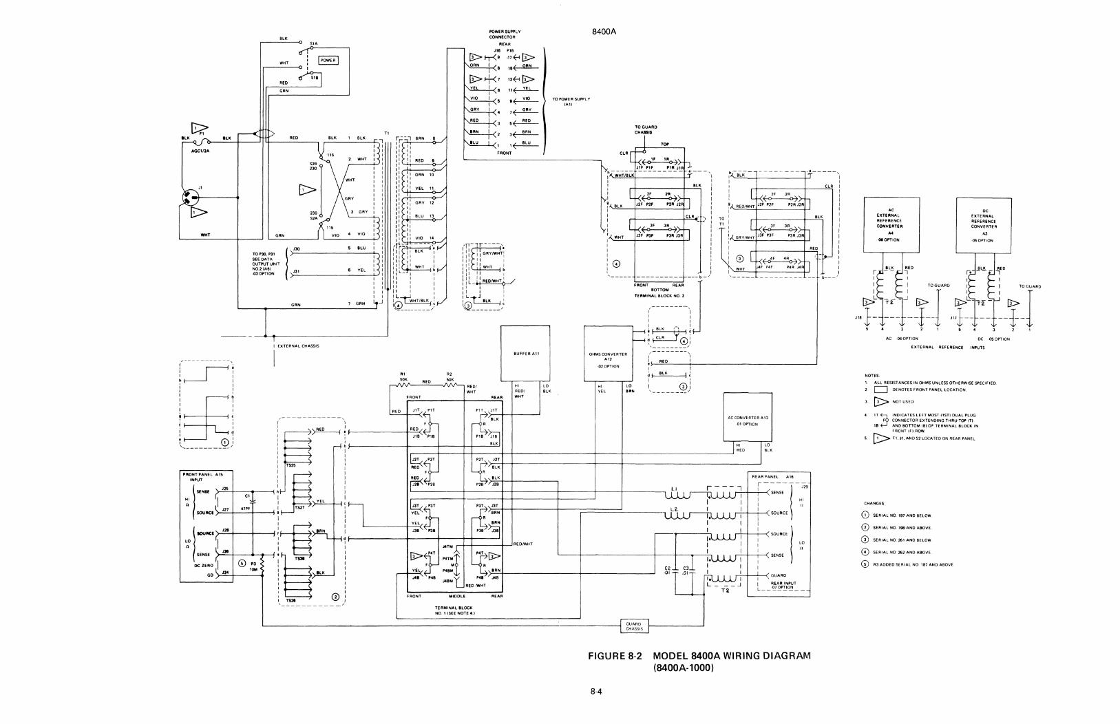
BLK SIA
WHT
RED
GRN
T1 REO BLK BLK
AGCl/2A
J1
WHT GRN VIO
BLU
TO P30, P31 l :JJO SEE DATA OUTPUT UNIT
:·~~~ >-J3_1 _________ v_E_L_......,
GAN 7 GAN
-------------------------~ EXTERNAL CHASSIS
(~-----------:
I I I I h I ' I I I
:~~ I I I I I I ' ~ , I ~ I I d I '
i, _________ <;2) -" /
(
TS25
P:lllONTPANEL A15 INPUT
J25 i--HI I C1
n SCURCI J27 '7PF
J21 i--LO I n SENSE JJI
DC ZERO I © R3
1DM GD
J2'
I I ,, I I I ,, 11 ,,
BAN
10
1' 11
ift~r--t+----> I I' I 11 l 1: L-_..----.
I I I I I I I I I I
0--r:WHT/BLKI; ... _________ ,,,.
RI SOK
FRONT
RED J1T PIT
R2 SOK
VIO
GAY
RED
IRN
ILU
RED/ WHT
POWER SUPPLY CONNECTOR
RE"AR
PIS
,17~ [i> 15~
13~(i>
11~
·~ '~ 5~
3~
·~ FRONT
BUFFER A11
HI RED/
REAR WHT
LO BLK
TO POWER SUPPLY (A11
8400A
CLR
TO GUARD CHASSIS
TOP
··---,\ ''-'""'-'.:.::!:9-------t-' I
BLK
I
I WHT
I I I I
© I I ' '
ILK l .-+------+-""'i I
---------- ---b-"'
BOTTOM
TERMIN~L~~~~~O-~ ( '1 I I I I
I I I I I I I I I I I I I I
' I I I I
FOONT REAR J ....---------. I _ I
~SBLK {1 s+
~t~~--!~) --------
OHMS CONVERTER ' '1 I Al2 i RED I -020PTION
I I d I BLK ' ~ I @! HI LO I
YEL ••• --------"
-·-----" I I I I I
• ;·~--'""t---------t-' I
AC CONVERTER A.13
01 OPTION
HI LO
I I
CLR I
b---"
I I I I I I I I I I I I I I I I I
.---+---+-1----+--+---------t---+------------~ RED BLK
FRONT
TJ:RMINAL BLOCK NO. 1 ISEE NOTE 4.1
REAR
GUARD CHASSIS
FIGURE 8-2
8-4
C2 •DI
REAR PANEL A16
i-~.:;-!-"" I HI I
..--'--+-t-I ---< SOURCE
SOURCE l LO n
..-'-+-+-< SENSE
~-+-+--< GUARD I I REAR INPUT L---~~.!_!0~--
MODEL 8400A WIRING DIAGRAM (8400A-1000)
AC EXTERNAL REFERENCE CONVERTER ... -QI OPTION
RED I
I
I TO GUARD
I I I O>t.:_T"f" _ _J (i>
J1B }- --f--2
I I
DC EXTERNAL REFERENCE CONVERTER
A3
-05 OPTION
O>e:-,.~ -
m}--
TO GUARD
O> I --{--2 I
AC -06 OPTION DC -05 OPTION
EXTERNAL REFERENCE INPUTS
NOTES:
ALL RESISTANCES IN OHMS UNLESS OTHERWISE SPECIFIED.
2. D DENOTES FRONT PANEL LOCATION.
J. [!::::>. NOT USED
4. 1T 3 INDICATES LEFT MOST ClSTI DUAL PLUG F CONNECTOR EXTENDING THRU TOP !Tl
18 AND BOTIOM 181 OF TERMINAL BLOCK IN FRONT If) ROW.
5. [!:::>- F1,J1,ANOS2LOCATEOONREARPANEL
CHANGES·
© SERIAL NO. 197 AND BELOW.
0 SERIAL NO. 198 AND ABOVE.
0 SERIAL NO. 261 AND BELOW.
© SERIAL NO. 262 AND ABOVE.
© RJ ADDED SERIAL NO. 187 ANO ABOVE

PliD -3
PllD-'5 ~RE.O
PJI0-7 ~ PllD-1 ~
7 PllD- 9 ~-
Pl.,- I I YEL
Pl<trl5 ORN
N01ES: ALL RESISTANC[S IN C>HM'O /I.ND "LL CAP'IC.ITANCe,_
l~ l\.\ICRO!=-AE.ADS Ul\ll ES.:. O'TT·E~VJl~E SPEC 1i:.1t:D.
2. v D["NQT[<::.l ':~IC~l\.~AL COMMOl\J
3 'T DEf\KJTE('." ... LO&IC ( OMMON
4 @ DE"-lOTE'- INffRNAL AD.JU'>Tl'llEN1
5 Q::::> R\/ MAY BE OM\T1ED DUf:.lt....16 A.D...IU'::>TM£P\Jl OF t".>V SUPPLY
RI 510
R2 IDBK
CRIO R5 51
+ C2. CRB ¢250
7
2.SO 4"
QI
Q2.
R4 40.2K
2
"'.>
R.11 500
+JSV
QC:.
?>
+IBV
-- -----·- ---------
+I C4
~50
-~--------
+IBV ADJUST
RIO Rl2 IOK IOK
Rl7 .22.0K
Q>
+~~~
RI+ 9.53K
+200V Pl-I
~ ~ +IBV ) Pl-4
POWER SUPPL'{ RO:F
Pl - (o
-IBV Pl -2
;L,,_, Pl -B
+5V ;>Pl-7
Rl5 40.2.K
FIGURE 8-3
8400A
A1 POWER SUPPLY PCB ASSEMBLY (8400A-1001)
8-5
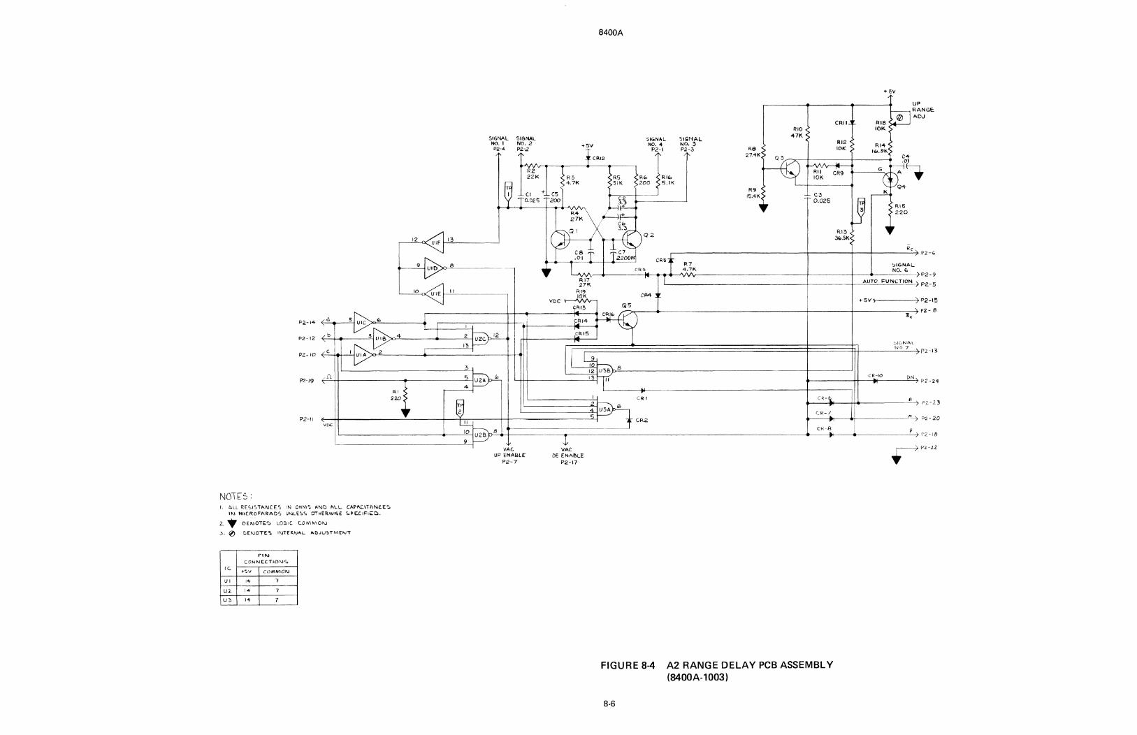
P.2.-14 a
P2-12 b
PZ-10 c.
f'2-/9 fl.
P2-ll VDC
NOlTS: ALL RES.IS l"M.JCES IN OHN\'; AND P.LL C'-PA.C\l"P.NtES IN N\\CROFAR:ADS UNLE"';)S Oi11ER.W~E S.PE.Cl~l~D.
2 .• DtNOl"E':> LQ[;,1( COIVllVlD"-l
!>. © DENOTE'S. l"JTfR.t\JA.L ,t\D.JUSTM[l\J"T
... "' COJ.JNECTIOl\.lS.
IC +"'.JV COMMO~
UI 1+ 7
U2. 14 7
U:> I+ 7
SIGNAL NO. I P2-4
SIGNAL N0.2 PZ-2
R2. 2.2K
---'l-"'2-a<"' U IF l-'-1.=.3 ____ _
10
4
RI 220
2.
I~
3
5
4
VAC UP ENABLE
P2-7
8400A
CRll
SIGNAL SIGNAL
-t- 5V
UP RANGf: ADJ
+5V NO. 4 NO. 3
CRl2 ._~-~~K~--+-;~ T~. r Rl2 IOK
Rl7 27K
Rl9 IOK
YD C 1---"\.f\l'I,-,
CRl3
VAC DE ENA~LE
P2-17
Q2
CR3
CA4
CR9
Rl3 31..SK
Re ------------------.l..------'----'-------"P2-6
R7 4_7K
SIGNAL
NO. G -) P2-9
AUTO FUNCTION ) P2.- 5
+ 5Y \------4 P2-15 ,.-~ __ __.,__ __________________ _... _____ _... _______ __,.pz-s
8
CRI
CR2
FIGURE 8-4
8-6
:Sc
C R-1 ~-----~~-----~-M-"7 P2 - 20
Ci<:-8
A2 RANGE DELAY PCB ASSEMBLY (8400A-1003)
.--)P2-22
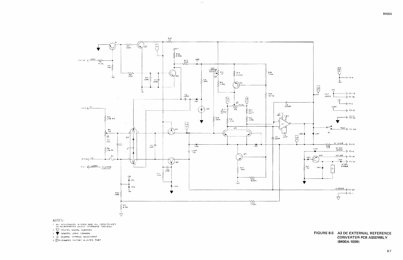
l\ID1ES:
p ~ - I t!> (---L_E_R_O __ v'.._'"i V-----e
"\-17K.
-IBY
•~o IOOM
ALL RES\STA...iCC:C:. lt.J DUMS Pri,...iO ALL C,.,_PACITANC£":1
lt.J MICIWFA~ADS Ll>JLES., OT~tRWISE '>PEC.ll'l~D
2 V' D(>JDT~'> SIG>J"-L CDli'\MON
3 • DU.lOTI:',, LOC>I C. COMMO>J
4 @ D[.f\JO~S ll\ITLR:NAL ADJU~TMLNT
5 [j::::>. D.LNOIEC:. FACTOR."f' SE.LEC..TEO f"'"'-liC..T
• 18\I
CRI
C.RL
161/
-~~:r- ~'11--IOOl'F
~- ----
-IBV
-r Cl
0.4"7
i...:11
ilOK
H
.. ,o
'"'"'
4t1PF r
tlOOV
Q5
CR?>
l -1sv
Rl'° Q,"'(ol(;.
R32. IOOM
. ., .. 7.l"':IK..
c .. Z7.0PF
C9 C7 33PF 220PF
CR&
CR.I\
RZ.7 IK
8400A
~ P3·4
·l&V
tSV
l'JOT ~ f'~· 1'5
USED p~ ·IC..
tif>
~ Pl·2.
t-200'\/
1 ~ n-13
~ I •• ____ v_Rc,EocF----)) p ~. 2...•
' CR.,
Kl
R'Zt. IL"-
CRIO
QIO
CR\2.
FIGURE 8-5
"' 50.J~E P~~\"'J
DC R'E"F DE.FE.A\1'
P?>-1.
E.X1 REF 'P'!·I+
Ci.I°?)
) .i Pl-'l.'
, NT, REF. Dt~1'l!:L..E
LDSE>J'!>E ) n-<.O
rP~-1
A3 DC EXTERNAL REFERENCE CONVERTER PCB ASSEMBLY (8400A-1009)
8-7

EXTERNAL REFERENCE INPUTS AC
HI Cl P18-3 <--------~ 0.22
Rl 1 .11•
lOOV SO~HZ
K2R _:....o--o----- 1------.~----'\J\A---.-----f-..!
LO P111-4 f-------~
K2B
., .. , ... (----~1
EXT REF
TO GUARD CHAlllS
0
C2 0 .25-1.5PF
CR!
CR2
••-18 -----------------------~ DC XREF DEFEAT
P4-S
VAC P4- l 4
CR7
voe CR9 CR9
P•-13 1 NT REF CR!O OISABLE
P•-2•
""i CR! I
P-4-21
1 VRC
10 VAC
1 DDVRC
Kl
R11 590
K2
RlO 9 .2K
ClO • • 1
Q2
Rl2 !DK
Cl 1 12&
RlS 120K
1 ,-1
I I I
2 I I
R19 n
R16 1 lK
CR3
11 ,-----9 I
_J
Ul
L ____ _
R21 •o .2K
10
R13 15K
---------,
AC REI"
I I I I I I
,-.!'2.0! _____ +---- ' / I \
111 I I I I I
SlA
1 VRC
10 VAC
100 VAC
OC XREF
ONLY
I
0 C3 o.e TO ion
1 V SOKHZ
RS 2.S73K
R20 n
C9 3PF
8400A
RU 120K
RU 8• .&K
0 1 V !KHZ
C16
~ 0.01
Cl• •• 7
ClS i 50
+19Y
R30 lOOK
0
0c• 0.8-lOPF
CS 12PF I OV SOK HZ
R7
10
L - - - - - - - - _'---~-...... --~"\f\JV----.1\/\1\.---_.... 220PF
FIGURE 8-6
8-8
CI 7
i0-01
R2• !OK
R2S
21 -&•
R27 21.5•
RH !OK
+18V
Q•
CHANGES
R22 •O .2K
+18V
0 SWITCH SIC ADDED SE ... NO.'S
CR&
RH 1.UK
123, 125. 1211, 131, 133 ANO ABOVE.
® ADDED R53 AND R5~ SER NO. l~Q AND ON
CR&
R36 1.!96K
TP
R39 130K
R39 12S
A4 AC EXTERNAL REFERENCE CONVERTER PCB ASSEMBLY (8400A-1008)
R•2 lOOV !KHZ lK R47 !OK
0 en
a.on HI SENSE
~---+--<l>----+---+--cY ~ P<-23 Kl A
R•O 130K
NOTES
R•l •DK
R,2 !DOK
+llV
h. -lBV
R•9 •87K
NOT +SV
USED
+18V
~ -18V
CRI3 CR12
VREF
...---<1--._--<Y ~ P•-19
R48 100
LO SENSE
:
K18
P-4-1
P-4-2
P<-3
P4-1S
P<-16
1. All RESISTANCES IN OHKS ANO All CAPACITANCES IN KICROFARAOS UNLESS OTHER• !SE SPEC IFIEO.
2. ~ DENOTES SIGNAL COKKON.
3 •• DENOTES LOGIC COKKON.
4. 0 DENOTES INTERNAL AOJUSTKENT.
' ~~}"'""'" """"'" "'
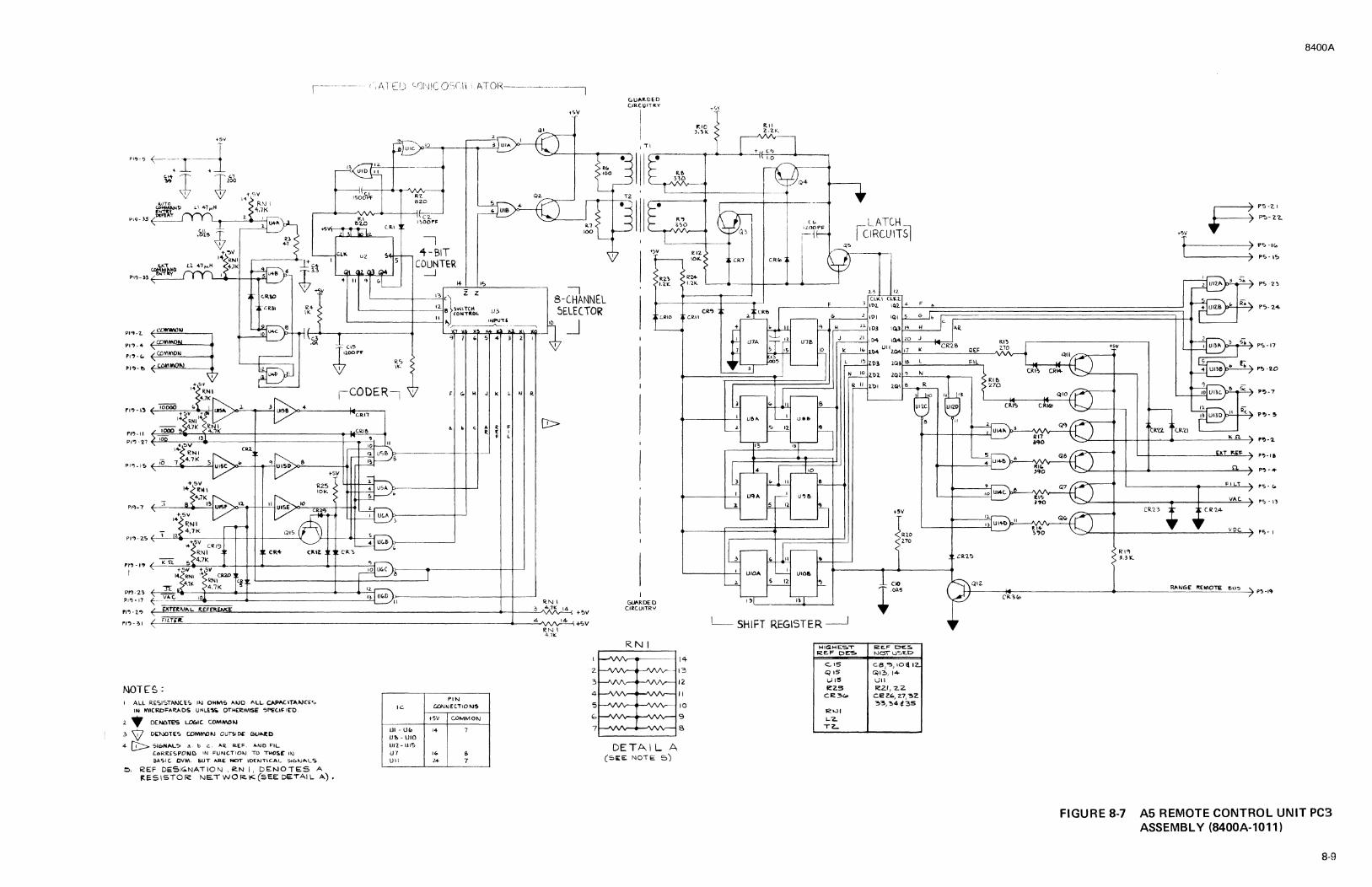
1-·----·-
PIQ- )5
"'"-~Q~r BZO j
r---+--./\/'Vl.r--<l>--+---lf-;:z:-
..;,,._-. .... ~"--'io~1 C.R.\ l'::iOOrF
Pl.,-'Z... COIVIWJN
Pl.,-4 CDll'\MO
J'l'j-(o CDr.'lh'\O'l
Pl'?-b ~l'J
r1">-•)
Pl~-11
PJ., ·21 10
Pl°l- !~ 10
Pi~-7 :r
Pl">-2':1 I c•19
RNI CR-1-
(: K st 5 4.71( ,,, _ ,.,
I if NI ~ 41~
PM-2~ ~ _ _YA.C. 10 Pl"J • 17
Pl"'}-2.' £ATFCP.IAL
rr"l-?i1 ~- FILTr"-
NOT[£,: ALL RE.SISTMJU<; IN OHM$ MJO ALL CAJ>l'ICITAl'JC~S IN h'\ICl<Ol'AIU.DS UNLE% OT"M~WISE ~/'EC.I~ IE'D
• DE.NOTE'S LD61C COMMON
3 w DOJO•E<, CDMl<\llll.J OUT~IDE l'>UAl!O
4- [I::>. 516NAL? a_, b c.. A~. R.EF. AP\10 F"!L
CoRllESPOtJD IN FUNC.TIOtJ TO T~S.[' IM
BASIC. CVM. S.UT #\R.E: MOT ID'fl\ITlCAL S16"1ALS
5. li<EF DESIG.NATION, 12.N I, DE'.NOTE:S A !tE.SiSTOR NETWOl'i<(SEE D5:TAIL A),
IC
Ul - U"
I 4-BIT
COUNTER _J
FG.HJl(L..NR
PIN co.J~EC.ilOPtl.I~
t5V CDMMON
14 7 U'b-UIO
UII-UIS U7 , .. & Ull 2+ 7
D>
RNI ~ 4.11( 14
>5V 4 14 ¥.>V
RN I 4.lk:
G.U"-"-DED C.IRC.UITRY
I
LRIO
GUARDED Cl2CUITRY
RNI
DETAIL A (5E:E NOT\:: 5')
14
13
12
II
10
9
8
•12 101<.
CJl.11
I~_
Q5
CRl' CR.kl
l)qA. U'll ,,
UIOA UIO!. ,_ 12 ">
SHIFT REGISTER __J
HIG~ES.T R.EF D~
C.15 Ql5 Wt:! ~ZS
C~3<o
R"-11 t..:z ..
T'Z...
L; ,, u.n
\Ql 4-
IGll
\Ql l"t ~
2.Q~ If.
ZGlZ o N
+5V
RlO 270
CIO
io>-•
fie.E.F DC:S. ~c:rr-usE.D
C8 1 "'>,10QI~ Gll~, 14-lJI I R:Z/ 1 22.
ce z.:., z.7, '3Z 33,34(35
8400A
F P5·Z. l
P':>-Z'Z..
>$V
t P?-IC.
) PS- l?
P'>·n
P">-2.4-
AR.
RI} C.R2.B
QE~ Z1D p~ - I?
<OIL I'!> -:io
•tB 270
P~-7
P'!>- !>
"n. P~-'2.
H l'J;F p,.' 6
n P~-+
Fl LT l"'l:j·(,,,
VA.C. !'t, - I~
CR'l.3 C R2.4
voe. r<,- 1
CR"l.?
QIZ. H----~------------+-------RA._N_G_E_l'!_Eh'\_D_>E __ ~_u_~-~ P':l·I~
Cl'-><c
FIGURE 8-7 AS REMOTE CONTROL UNIT PC3 ASSEMBLY (8400A-1011)
8-9
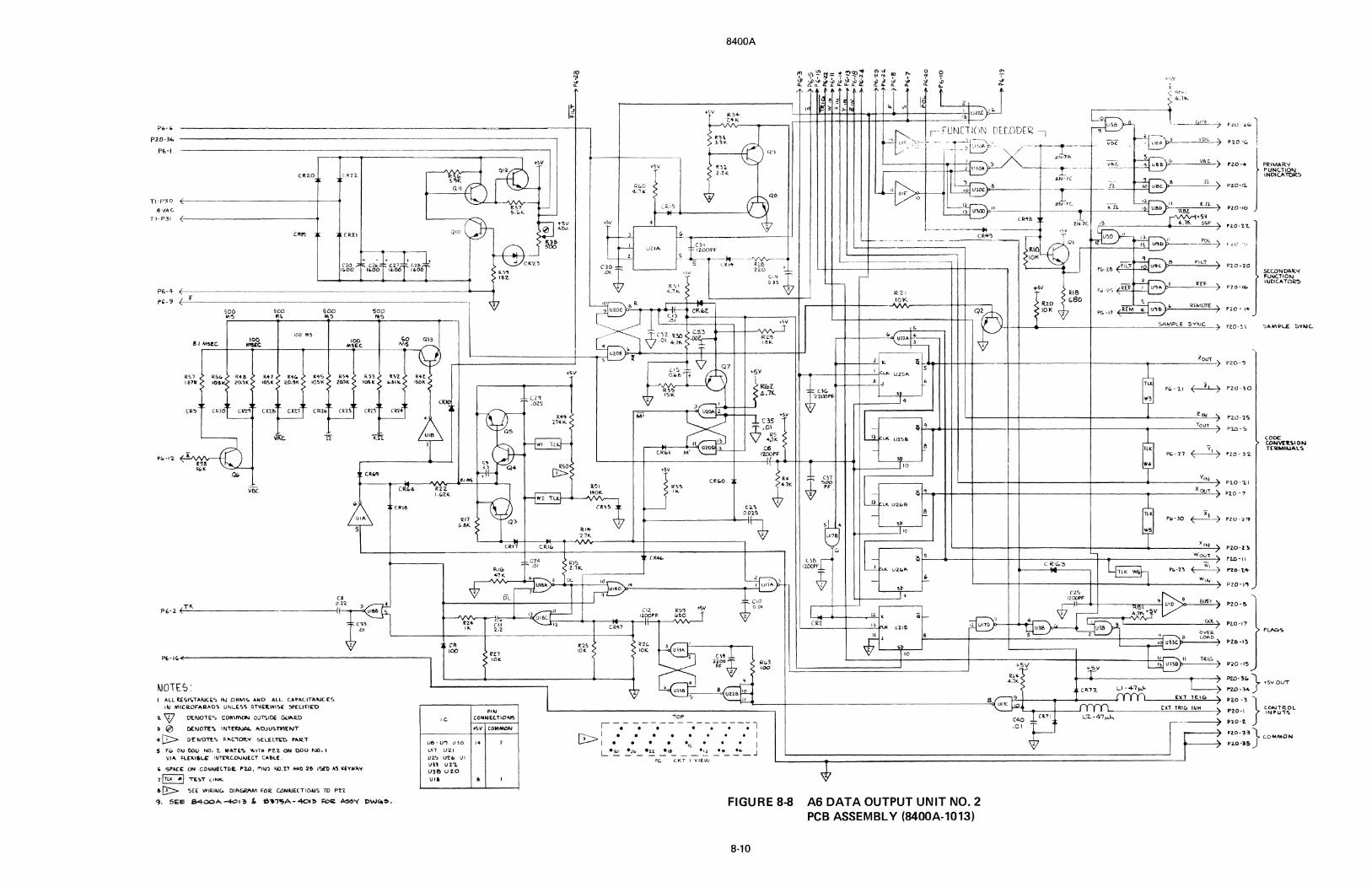
PC-b
P20-3<.
Pb-I
T1-P30
B VAC
Tl-P3l
CRZ.O
f----·------------+-----
U.i'2
CR.2.\ QIO
C20 IC.DO
---1--~ --i + • + + --- JJ-
C:lfi> CZ1 l.l.& lbOO 16'.00 1'00
P6-4 ~ P'-9
f
500 ,..,
8.1 MS~C. 100
MUC
R51 . , .. ... J,B7k 10• 20.5K
CR'7 CRJO (Jl'l,O)
VDC.
500 500 M' "'~
100 M5 100
MS£C.
R47 .... R<O ., .. ~051( 2.0.51( IO~K ZO.,K
Ci:.(.b CR'l.1 CRl" CRB
---1
500 NI.,
R51 IOH
Cl1'.l
,0 M5
l52 "·&IK
Ql3
CR 100
P6-14~-----------------------------,
hlOTES: I ALL R£Sl'i.TAMC(."l ttJ OKMC:. AND ALL LAPACITAl\lLES
I~ M\CR.Ol=AR"OS UNl..E.SS OT°"i."WIS( :::>P£U~lk'O
:i. w DEl\lO"TE"> COl\'\mON OUTSIDE GUA2.D
3 0 DEl\lOTE':. IN1~1'hll>L l\OJU,Tl'lEl\lT
4 Q::> DENOTE~ ~/l\C..,.OR,.I( s.ELE.l~ F~R.I P<Q O~ OOU NO, 'Z.. VHffE~ \\ltTtt P'Z.~ ON 000 NQ, t
VI .... REX.I&~ ifJTt"R.CO!VhJEC.T C-'~LE.
' 'SPAC£ ON CO~f\IEtiOIZ. PW, ~fU') t-JO.'l."7 MolO 221 ~A, K''l'W1'.,.
1 l1LK •I T[.~T LINK..
6 [!:::::> 5Ef. WJRl~G DIPt~M fOR. CilNUECTIOIJS TO Pt'l
~. SIO.E 6400A-401?> &. 8'1'5A-40t~ F"o~ 1><:6Y t>W~~.
IC.
vs - u-, u ~o un u21 UZ"J U'Z.b UI
un UZ'l. U38 LJ ~O
Uli
rz1 10<
PlllJ
COa.!MEC.TION'l
.+o:.V COMMON
"
I~
·~5 IOK
.___--+----------- -
•SV
C30+ .01
'
R~O 4-.lk:
+?V
LJ2.IA.
CR4'o
Cl2. 12-00l"F
WP
8400A
1-.- -.--.----.--.--.--~1
Q.>11 • I •,s l L ·~ ~i&_ ·~ ~1e ___ •.:.!.. ~s- ~+- J
PC. Cl<.T I vrE.w
RZ."J LSK
1<03 100
FIGURE 8-8
8-10
l- . - -- -----+! [f(,.q.<")
' unA
l 1 ..
5 CLK UZ?A.
4
~ ' LI< U2.~B
10
Q'
LK U2.C..B
,. IO
i!i uzw.~
,p
IL .. Ci 13
U< u21e
10
A6 DATA OUTPUT UNIT NO. 2 PCB ASSEMBLY (8400A-1013)
,---L___J
+'-~'!
no H· l I
P2.0 -~ \
PZ.0-1'2..
P20-ID
FUNc.1101\l INDICl\TDR:.
J PRIMA.R.'f
) rLO·H. l , ___ POL--) ~ :.:_(} .. '-'
FILT P2.0-'2D
t>-----•~EF __ )-> PZO-IC,,
5£CDNO~Q.."( FU~C:TIOf\> llJDICA.TOR.~
REMOTE
louT ) PZO-_,
Pt::O - 21 ~ PZO·~O
ZtN P20-2S
YouT PW-S
CODE C.ONV('~!>I ON
~ TERMll.IA.L~ PG.• '2."7 l'lC-~2.
Y1N P2.0-'2.I
X OlJT no-1
PCD-}Q ~ PZ0-2.<J
'1N P20·Z?. WouT
r2.0-11
~ ptO-t.~ w,,,
PZ0-1,
BU'lY no-t.
GO- P1.0 ·Ii Ov<R FG'&S
LO"'D PZO·I~
P20·1S
PW-'r..} t5V OUT 1"2D-~
PW·~} CC>f\lTROL ~20-1 INf'UiS
Pt0·2.
"0-~3} COMMON P.2.0-35
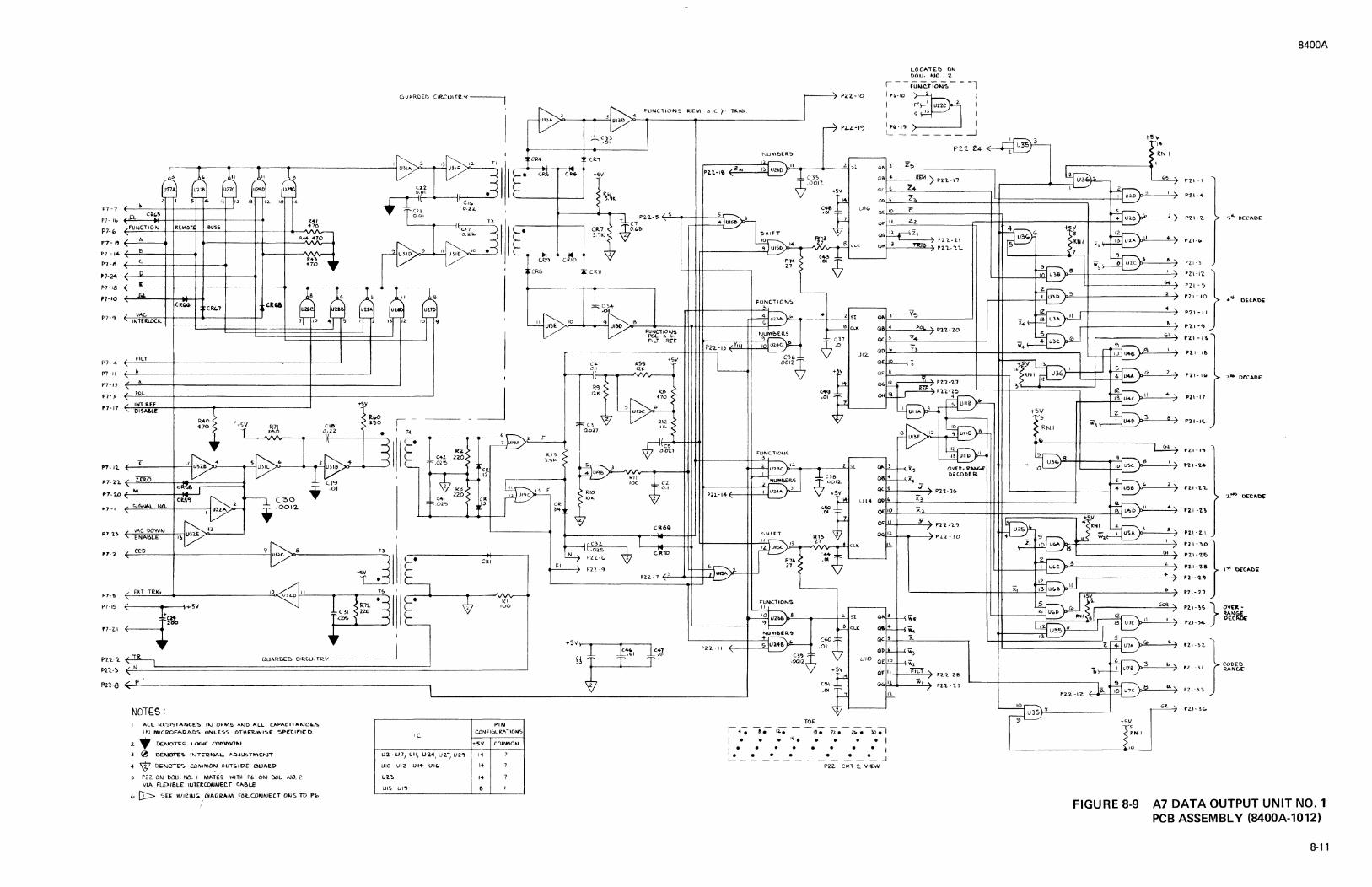
P7-"
P7- I' A.
P7 ~ 14 ~~B~ _ _._.. __ _.
P"l-B c.
'7·24
P7·18
P7·10
P7·~
p7 ...
P"'1·11
P7-13
P7·}
n-11
P7-ll.
E
VAC,
FILT
POL
llfl O.EF
p 7.1.l. ~_,z..,,E.,,R:O __ T;j'!~-;:::::===::::::
f'7-21J ~"""'-----+-~---'
P'7-I
P7-l~
•7·1..
P7·15
f7·2.I
t;\E,NAL NO. l
VAC DOWl\J ENABLIO
i-(-----~~-~1 ... s11
.l!cn
~2~
13 12. 10 ..
C:IO i .0012.
"41 HO
+5V
GUARDED cu~.C.UITRY --- -
NOT~S: ALL RE":>l5TANCE ~ I~ OMMS A~O ALL LA.PA.C.ITA.NC~"!.
IN MICJZOFAQ.A..[)S UNLES~ OTM.£R...WI':.£" ~PCC.IP'IE'D
2 • OCNO~'=r. LD61C. OlMMON
3 0 DEMOTE~ INTICTlMA.l- AOJU'STMENI
+ w DIOtJOTIO<; Cllll'IMOl\J OUT~ID( C!IUAlP
5 P22. OM OOU. 00. I MAT~~ WITH Pb 01\J DOU IJO. 2 VIA FUXIBL£ 1.iTERClWl\JEC. T CABLE
SH: \VlitlU~ OiAGllAM FOR.CDl\Jl\JECTIOUS TV PC.
I
GUll.RDED CllU:UITll.'1'---~
1-
_J
IC
U2.· LJ1J u11, U'l.4, u21, U2"
um UIZ. UI+ UIC.
UB
UIS UI.,
_J
PIN CDNF"lbU£.~TION'So
-t-S\f COMMON
I+
&
F
LOCA"T£D ON DOU, f\.10. 2
r - - FuNC.T IQ,.; - - -1
""--o------+------------r P2.2.-10 / 4 J:UNCTIONS R.E:M. b..C Y. TR1t0.
I ••·10
I
I••·" I
" FUNC.TIOl\JS POL. &. b. FILT RE'~
res "{7 o.oz.i
C2 0.1
CR69
FUNC.TION.~
Clb .0011~
S:-UNC.TIONS II
Pl.2.-1.,
__ !_ ___ 2 S.t
e C.L.'IC.
..IC37 v.O\ +~V
U12.
L ______ _J
P2.2·24
QO + P'2.'l.·11
<0c,_,s~-z~------~ QP~·~-~Z':2._ ________ +,.:::f=:=:=:=:=:=:=:=:=:=::;---r-4 QE~IO~ __ c _________ +-h
'---~ '21.·ll f-'.'---'-'"'"-~ P1'l.·'l.'l..
,,..r--i __ V~5-----~ QB,_~~--~""~~ Pl"l.·"20
QC""'" __ v~-------+-~ QD~·=---y~~'°--------1---+1--------~ QE 10
.x..,s'--' ___ _.. P2'Z·'lW
Ul4 Gll>~~'--1---""----~~~-++++._..--------4 QE 10
QFf'l,,_I +---''--~ Pl'l ·'l.,
QG~l'--1-.--~ P1.1. ·JD
"
I~ U2~ 1>"8 _ _,,_ __ t-=2.-tSl
'--------+--'-!>-- 8 CLI(
PZ.2. -II
r .. -; I • 1: '--
TOP
•• 12.e e e lf:Je
• • • • •
UIO
C!ll .OI
n.-~.-l:>;-1
• • • I •
• • P22- CKT 2. VIEW
•5V 5 RN I
FIGURE 8-9
8
6>
..
..
61
l
..
b
Gt
Pll -l
Pll-'Z...
PZ.1-W
PZI-)
;:: .~:} 4tj. D~CP\.Dk P2 I - II
Pl.I ·<I)
Pl.I-I~
Pl.I-I&
P2.1-IK;
Pl.I-I~
'11-'Z. ..
P2.1-'Z.'l.
P21·B
Ptl • 2. I
::::::} ,...,,. OE'C.A.D~ '11-1'1
PU- 2."1
P21·~S} :~~~ DEC.1\0£
l"l.1-}4.
f'21-3C..
8400A
A7 DATA OUTPUT UNIT NO. 1 PCB ASSEMBLY (8400A-1012)
8-11
P8·'Z.I
I MASTER I QOCK
RI '> 75011..
+16V
P8·7 L~,--'··F-----t:::========================t.-.J_ __ __'c~R~l~O--------.! CRll
" Sl6l!AL tJO. I!> P8• I '
Pll·'l.7 (-~~M=O=D~O=UT-'--------------_..-.i--+-. • <'..'R1
1 +•5-v--------+-~ CURRENT ~ RB • R' RIO.
CONTR.OLLID ~ IOK 27K 114 ~
l R<.S >Ill<.
·16V
OSCll.Ll'ITl~ /;~
) ~ Q2 Q3 '-=>'---+--i~ L::B
.. ...
P&-4 L CCD T LIO
2.~~0~111~~~-L-===============================================================-~1+ ~1~1 _,1---~~--l~........j.4-+-~~~~~i-J P8·'l.0~ ~ FZ'>·l-4 < MOT U'>El> l ~
Pn·'l.') ~<---~1
:::.:.9:=r: PS-IO ( -
rs -'ZA-
-17''/ REFERENCt SUPPL"( r
~Rloi[}> >
}~~~ > .m.~
..... ] ,__ ___ ·_'!:f_~.,_K __ -l~-11 Qll
~\ "' 1.0:.1<.
~ri ~( 2.21(. ~Q1"3
CR& CR.°' ......
tW
1
STORE 1!1 S2~ 7
r:n-zt
P2?>·.,
P2S·'I.+
P&· I
P8·8
STOltE OUT-lo PH- 5
~_.J 7
~~ 'Z.Zt<.
-161{
J\.AA
R4"l Ill<.
~R'>O >i'l.OIC.
'---lf----+-4---'l'"'~.__ ___ ._.:z._"---1--+.1 Q17 ~ ~1 ~ ~.. J -\!:_ Gl'>~ll~ ?2';·11
P!.~'21•-,
P'l.~-'l.~L~----...-----------------------------J °"L V R~F j
Pll·'l.'I'\"
IC PIN
CONtJlti IONS
COHllllON
'" , .. 7
8
I. ALL R'.ESl!>TAl\JCE<;; ltJ OMNI'=> AtJO ALL !:APl'ICITANC.l<S 1'-1 11\ICROFARAOS. Ullll.£.S':> CTl-IER.'11/ISE 'l>PEC.IFIEO.
2. \J OEtJQ~<;, SIC.NAL COMMON
3, • DDIOTS:~ LOIOIC. COMMON
... (!::> DE:NOTC">. MATt~ED 'aT
s. '2J 0£.NOT?:':> IMTE:RNAL l'IOJU'5.TlllENT
(I.~ '=>EE WIRlt.16 011'1&.l:AM l"Olt CO~lllitTIOl\I~ "TO PZ+.
~----1 : : •• • I • • • • 114-·-~~~
TOP'
-t&I/
<,,!\!.?. ~ U.OIC.
-l&V
'VVv
-. - ~ -; -,,, • • • • • I
• 1i;,• • • •
_,e IL1 8 1 __L _J P2~ CK1 -.-vlEW-
FIGURE 8-10 AB LOGIC PCB ASSEMBLY (8400A-1004)
8-12
J / ..__,_V~v,'\J~'\.,--'
___ ,... ~\.-Q'-10_~.------· '•_av __ z_n_. _ _:z.::E::=::.•4" Pu ·•'!I f ~ ,
-f~Y .._ _ _,,JW~'VV,\..j(,v-...J]
<> R•~ ~ 47tc..
-t&V'

P24 17 SlDRAGE lNPUT f------- ··--··-····---- .... -
P24-S
P24-20
P24-22
1'24-9
P24-2.4
P24-26
~--- --=..::..:: __ --- ------------------------
~ I 11 ~ - ------------------
P9- llil
P9- 16
PZ.4- I
~~.fr ( POL INFO_A____ j (GATE 4
1 GATE
4
--INVERTING AMPLIFIER----
R7 IOI<.
pg-.2 <A TO 0 INPUT
P2.4-.14 ~-----~~
P~-25
P24-2,
-----------.---,VREF
PZ.4-21 ~-----~ P2-4--30
PZ.-4 -32.
pg. 2.3
P2.4-28
P24-31
P9-i>
P9-2+
P9-5
P9 - I
P2.4-19
PZ4-2
f'24-7
P2+-ll
Ml SENSE
<--------o + t9V
-----1-ISV
ZERO
~GATE 2
~GATES 1.22 L GATE JI
RBI 4.7M
-ISV
R3 47K
R4 4.71<.
Rl4 20
.---POLARITY DETECTOR ----,
lR23 4.'!':tK
CR20
CRB
A/DAMP AUTOZERO
r-DRIVE---
8400A
LADDER I SWITCHES--------
SECONDARY PRIMARY rLADDE --., •LADDER ::::1
DISPLA'f STORAGE -., R+O 7501<.
A TOD AMPLIFIER------~
R2<i> sz.
+18V
-1811
CR.17
TOP
~I ·:;.- S. lz-; ;-19-; 2~ 2"-; 30;-M;. l I •• •• •• I.. .. .. .. .. .. I l ~I ·-~-~~--~-~~-_J
P2.+ CKT I VIEW
Q?>O
RU,
R-41 7!501(
R42. I.SM
270K
VREI'
R~8 R"t?> 8> "-2M ::IM
ANALOG 1COMPARATOR~ -,
-IBV
Q32
-l&V
'L>"----------...------___._M.;.;.;:..O~D_O::..:;.U_T~P.24--~7 ~----------------------------....,P~4-3
NOTES ''- ALL RESISTANCES IN OHMS AND ALL CAPACITANcr.c,
IN llllCFlOFARAOS UHLES'!! OTHERWISE 5PECIFIEO.
f. @ D£NOTE:S INTERNAL ADJUSTMENT
3. 90ENOTES SIGNAL COMMON
7. G> DENOTES "FACTORY SELECTED COMPONENT
8. G> SEE WIRINli DIAGRAM FOR. CONNECTIONS TO P23
4. ~ DENOTES MATCHED SET
5. 8:> DENOTES MATCHED SET
6. ~ DfNOTES MATCHED SET
FIGURE 8-11 A9 A-TO-D CONVERTER PCB ASSEMBLY (8400A-1003)
8-13

~10-~ •F'ILT IN
R7 IOOK
PI0-10 :rtFILT
CR-, KI
PI0-9
+IBV
-18V
8400A
+19V
RIS 7.ISK
C7 150PF
.. 1sv Rl5 2:49K
A TO 0 IMPl/T PI0- 4
-l&V ~ +IBV~PI0-1 ~PI0-2
Cl .•n
RI.+ IOOK
CR2.
NOTES
RS 8.blOK
-IBV! ) PI0-6
I. A LL RESISTAHCES llt OHMS AllO ALL CAA<>.CITANCE 5 IN MICROFARADS UNLESS OTHERWISE SPECIFIED.
2. ~ DENOTE"' COMMON.
3. • DENOTE'S LOGIC COMMON.
4. D:> FACTORY SELECTE'tl
5. @ DE.NOTES INTERNAL ADJUSTMENT
FIGURE 8-12 A10 ACTIVE FILTER PCB ASSEMBLY (8400A-1013)
8-14
r--- INPUT
• l=llOM T!ol J41M :.ko~~NO ro::~~~/.--0-. __
I
KIA
RB IK
R"I 100
RIO .,.,,"tSK
"-' IM r. -:--
I
' •4
© IOOV
0 1000
rn 22.0f'F
R~ ~IOK.
1 -- - CllkR~ NT
K7A
R.12 r~;n:
cs 2.70PF
R2. +71<.
-1e.v
CCRI
-l&V
r () If)-"-· .-, \•Kl I .. - --1
11\JPUT b!A~ LOh'IPLNSAllON N("tWQRI,(,,
l?.17 lOOt<...
:~~~::~~R >-=~=D K---<~-~l>------------.... -~----~o-,_ OIA.C:ii.A.N\ ~
CR.& K18 +1&1/
FR.OM T1&1 JITM)'>--"-L_u ___ -"J -18V
Pll-'Z.0 b'
c:· Pll-B.
Pll· I°> i:'
Pll-4-VDC.
._,
_fl CR.17 Pl 1-14- ~(_::c:;_ ___ __..,IJJltl-
Pll - I ~-------------------------Pll-'S c'
Pll-"7
p11 .. 10 < KC.. CONTEOL
r-- AMPLI Fl ER -----·1
COARSE DC.
ZEO.D
R'Z'l.
[1>
R'P.1
Q::>
I BOOT5TRl\PI AMPLIFl[R
""' IOK
k''i'..~J
O'>
£2C..
[.·-..
"'o '"'·
kl(
~ILTER.
'"
8400A
PU-IC.,
I GAIN DETERMINl>JG NETWOR~s ]
ca 0.1
"'~ 20
i-181/
T
BUHEE..
)
Pll-C.
Pll-3
Pil -11
Pll • il>
Pll ·II
Pll - 12
Pll-1'::>
ZER.O .----".AJ'V-------4 Pll- 24'-
1<40
Kl CONTROL
NOTES: ALL RE'.l'H o.NCc;:5 It.I 0111111<; AN 0 ALL CAP'-CIT"l\lcr'.. ll.I MICROr-A.R.Jl>.Oc;. U~LE'::.~ OTMl;:1tw1c~e c;p&fF°l~O.
2. '\:! DENOTE'~ SIG.~,._L COMMON ,
3 • DENO'!'[~ LOGI( COMMON.
~ c:>- DENOTE'. FACTORV "8.£CTE:D COl/IPOtJEt.iT. M~'l l\kJT BE llll">TllLLED.
5 Q::::>. 0£tJDTE'3 1\111\.TC.HED (0MP'ON£NTS
' )!::>. J:3S R'!"'l A.~D R.3-, AR.E DIVIDE'R. ~£.T 7 e'J D£"l\JOT£"i INTE:R.U11.~ A.OJU~l MENT.
8 a:>- ~'7 1 R:C,.} R.:1 l\tJt) R.10 AR.£ DIVIDm ':'.>CT.
LO
RELAY 0.1
Kl • K'2.
Kl
I- K4
i<S
KC.
K1
e l~OICA."TE.S
LOGIC.
VOLT"G.E RA"-IGE
f;I
1.0 10 100 1000
• •
• • •
• •
• • • RELA'il E~fR.61t£0
FIGURE 8-13 A11 BUFFER PCB ASSEMBLY (8400A-1005)
8-15

,----, I TD2· J4 F '>-_:_I =B:..:L:..:tc.:.__~-----c-R•'1-~ I : i I
I "Ti!>l.•J3F )-41 I
IC.LR I •&a.- J'Z.~ l __ _ J
SEE >JOT!: 4-
+
L k~
' Pl'Z.-14-
/ ""
C.I IC.O
QI
C"!> Q'!I I
R'I. IQ.OK
~4
10.0K
l!j 'il .o ' ~.AA J If-/ D~
" "- ::\ 'V
Pl'2.-1"7
Pl'Z.·'l.0
Plt.·1&
Pl? -110
Pl'l..·10
Pll.·1~
111'11..·'1.1.
P11.·'2..._
Pl'L-1
P12 .. 2.I
Plt-'L'>
P'll·I'\
flt.· '1.
LI> ~:y-
' LR<.
' s. ' ,, .n
' L 0.
'
f-:--/ b'
" LC'
'
L CJ)
"
L A
' L Kl CONTROL
'
~
I~ U4D_!8 + lil34 0 Z.ZIC lil33~
'" > ·~ Jus0r. ' 1.l>I> 6 . :,/
1 10
~ 12 I~ USD " -
~ ~~ + U4A.J
• 5
CR~l '-"'"'-w- C.7
QOI+ --.
1 CR.9 ,... CRIO '-
~ ,...-CR.I~
> ~l~ > > ~l~
Fs 0 CRIG.
* Jv
R<-[i>
, CfB
[i>
R.1 II<.
R& 2,K
® 10000 .n CDUR":>E ADJ
.. ,, [!>
s
~ i I
'- ~RI~
re.
... v+
us
•AA ·~; ..
~ k>'I.
l!>.1.~
• l'l.0
• Pit.I
C.Oi.ll\lEC."TOR5
>'>VOC.
14
14
14
C.ON\MON
7
7
1
IOOJ\... 8400A
1000..n..
(J/) i!JQ Rl4 IOK 1001(.
IZl'Z RI& "'¥1-.1~ <..~~\(.
II.II RI~
4<o.<K %41<. 1001(
© OQJ
i<-1·&- I 10001 11001
R'l.l. R'l.I 70-~~~K 100
[§] R'l.0 777,l~K
1000()1(
®cw ~ RI& Rll
,,"1&1M 2'>1<..
R'2.'!> ::J '°"'"' 100
.. YEL CR'l. J IOI
CRl4-
~· I> ....
CF Kt. CONTR.OL
Q'!>
~ -"vV'
T R2.4 3"10
33 pf +ce >In > 2.Z"-
·~ r>:1.'> 3.,0
CRll.
~ ~4 +
j, CR20
NOTES: I. ALL RE.~l~TA.MC.£.'S l )J OMM~ l\ND "LL
CAP#\UTA NC[.~ ltJ MIC.R.O FARAO"!:o
UNLES\, O"T\1£RW15E !>l'EC.IFl[D,
2. T OCPJOTE-:. LOGIC. CDMMDrv
3. @ DDJOT!;:'.> INTERNAL ADJUSTll"l£NT
4. 5£E Wlll.IUC;;. 01~6'1l..AM
s.[J:::>- FACTOR"!' SELECTeD 'S!.I.
R35 ZZI<
t---R3~~
~ 221( >
..., CRl2. £lU QIO > lt'Z.7
Cl:>~ > ... ?\<.
LO i c;i.
0.01 ·--, l" ,... CRl3
FIGURE 8-14 A12 OHMS CONVERTER PCB ASSEMBLY (8400A-1010)
8-16
$R'S7 > llV\ 0Q& •AA
·~~. l\C.
V~EI:
HI )
LO
' 7 +SV
-7
§2. '\. 7
!KL ..... -7
.._UTO ~Ul\JC.TIOlJ ' 7
Pl2.·4
Pl2.·!
P12.·'=i Pll.-CO
Pl'l..·IZ.
Pl<-·11

TO Tll
F!LT P'IS-10
YAC P'IS-1
YllC INTERLOCK P'1'-9
P'IS-19 +llY
P'13-17 (
~ P'IS-21 ·llY
Pl3-5 +6Y
YRC ON ENABLE P'l,-2'
YRC UP' !NlllLf P'IS-1
P'IS-14 Ra
P'IS-IS ~
P'IS-7 ( + J
P'IS-15
a' CRll P'IS-2
P'l3-6 a'
P'IS-3 ii"'
b' P'IS-11
c' Pl3-16
c PIS-4
CR14 CRl3 CR12
iKl~i I Cl
l NPUT r - - - - ..J • 022 I
LO I F--+-<Y
!~--~
K2A "'----~~~~~-..~~~~~"""""~~__,,
CRI
CR2
K'
Kl
K2
K4
CR7
KS
CRI
Kl
CR9
Rll 590
Kii
L
RI& 120K
Q2
Rl2 !OK
Cl2 Rl9 500Pf 47
4~~~K
CR4
Rl3 15K
RZO CIS 47 IOOP'F
'
RU ID"
Rll UOK
Cl6 ~0.01
cu
·~ +7
+llY
11111 VOLTAGE ADJUST
RSO IOOK
Cl 7
~0-01
·1-16
CRI R22
40.2K
Rl7 U.IK
Q6 RS& l -702K
R28 81 AB CURRENT IOK AO JUST
R32 200
0 IOKHZ
NOTES
rr
~H~ 0.47 1
CRI
K'A
~=II R43 130K
R'7 J .702K K'8
R'8 125
l C25
~o~
~ @
io~~
R50 lOOK
AC ZERO
-!BY
CR15
8
R47 !OK
R48 100
HI a.111
8400A
KH A 'ILT IN ) PIS-12
~ C24 0.0047
~ LG l!N8f
1. ALL RESISTANCES IN OH"S AND ALL CAPACITANCES IN "ICROFARADS
IC P'IN CONNECTIONS
+6Y co""ON
U3 14 7
U4 14 7
UNLESS OTHERWISE SPECIFIED.
2. ¢ DENOTES SIGNAL co""ON
3 •• DENOTES LOGIC co""ON
4. 0 DENOTES INTERNAL AOJUST"ENT
5. D> THAU [)> DENOTES "ATCHEO &ET.
6. - - - - - - GUARD SHIELD
FIGURE 8-15 A13 AC CONVERTER PCB ASSEMBLY (8400A-1007)
8-17

lo
e~Z 3 I
I
lo I c~z
3 I
I lo I
0~2 3 I
I I
I E.XT1ReFJ
51
0 0 JIO
POWER SUPPLY
JI
59 .,
I
I
cl
~ I I
cl
~ I I I
~
I I
cl
Pl't
Jl't a.
~
I
-dJ--
Jl4-3 Jl]-10
Jll-IB
JCJ-1
J9-2
Jll-15
JCJ-24
JZ-21
J&-5
J~-.2
Jll-4
voe
s! 5
510
ol
I cl
~ I
---G---
J7-19
Jl-8
J7-li.o
J7-Z3
Jl-7
Jl2-23
Q37 J5-I
Jlo-1
J12- II
CR7
Q2.
7 511
0
I I
?
--8---
J2.
512 0
0
~
8 e
~--
Je-20
J3-21
J1-2.0
J7- 12
J3-15
J 7-13 Ut-.l)U2-6
R54 C~IO
Qllo
JS-7
J5"-5
J7- I
CRS
SI~ 0
I
--G---I~
l'I
DC EXTERNAL REFERE:NCE
J'.!>
16
I'
RANGE REMOTE BUSS +SV
111 isl 171 IS
SI+
0
REMOTE.
~ I I
ol
~ I I
ol
~ I
o I
?
J4-l'I J9·21
J~-21
J4+-ZO
C4 JB-21
J4- 15
J4-18
J4-5
..... 0
Jl-2 J"l--1
Jl-4
FUNCTION REMOTE
BUSS
131 1e[l 13 18
FUNCTION SWITCHES 58 THF!U 514
RANGE
SWITCHES 51 THRU S7
UIA-2.
JIJ-6 JIJ-1~
JI0-2
Jlo-~
UIF-12
Jl2·18 UIE'-10 Jn-4
J8-6
J/2.-9
REMOTE CONTROL
Jl4-17
CRZf. U2B-l'I
J'l-16
Jl3-8
JS
8400A
0 I 0 0 2 0 0 3 0 0 I 0
0 2 0 0 3 0
I I FUNCTION DISPLAY
TOP VIEW 51-514
~~~el----------.
BUFFER ANO ATTENU,.TOR
Jll
Jl2-ILf CR .eB U2.A-3
J7-2 I
CR2.9,Q3S UZB-13 Jl4· I ~4-18
J7-15
S<D,CI
J7-4 JIJ- IO R4 Jl4·9
l.114-11
DISPLAY AGSEMBLY Al+ ~----SEE
VAC. INTLll.
N!TE~
D D D D D [J D D 0 D D 0 D JI JZ J3 U4 JS JIO J7 JB J!I JIO Jll JIZ Jl3
r--, D L~': J
Jl4
CONNECTOR. LOCATION - VIEWED FROM TOP FRONT OF INSTRUME1'1T
J 12-2
VIC-ID
JIZ-21 ,)1:,-21
JIO-"'
JIO-!>
Jl2 -12
Jl2-7
Jl2-3
UIO-B
Jl2-19
J12-S
J'l-13 Jl~-s
UIB-4 Jl3-Z.
J2-13
Jl2- I
Jll-20 Jl3·1(o Jll-6
JB-19
OHMS CONVERTER
J 1.2
Jl4-9
Jl4-ll
Je-20
Jl3-18
Jll-7
JB-7
JS-24
Jl'!l-14 JI I• \'4
J7- /lo CR30 J5-5
Jl3-7
Jl3-5
J9 -21
Jll-2.2
R42.
Jll-IB R+2
Jll-17
J9- (o
J6·9
Jl2·15
JS-7
J7-3
Jl2.·B
Jl2·IO
Jl2-I
J2·7
RM.5 CONVERTEK
J 13
DATA OUTPUT LJNIT (PCB NO. 1) LOGIC
J2·17 J8·24 J5-Z2. JB-15
JZ.-2~
J&-ID
J5-l(o
J2-14
CR.JS
R<o2. Jl3-9
Cl\1'
QI"
J7
J6-/2
Je-21
Je-19
J2-20 Q:u .. J8-I"!) Jl2-12.
J2-191R~5 QI!."!> JB-11 JB-7 J2.•IB RS(, JJ2-9
J8-JO CRI
Jl4-13
Jl+-3
JS -(o
JS-+
en JB
FIGURE 8-16 A14 DISPLAY PCB ASSEMBLY SHEET 1of2 (8400A
8-18
PIS
Jll-I~
Jl2-18
J12.-19
..----------<FILTER
..------~~1U'~~E
FUNCTION SWITCHES
Jl2-14
JIO-S
R'I JS-6
J5-13
Jl4- 7
Jll-19 QJS
Jll - s CP.16 J11 ... z
J9 -13
u7-ZI
Rio
Jl2-.20
J2-2..4
U4-Go
u4-+ R61
U4-7
Gl2.5
J7-l+ azci J7-S
.CRIS
J7-15 Jl\"'3 Jl+-1!5
- J7-2
J.,-5
U4-I
J-l·Z
J'I- 3
Jl-4
ATO 0 CONVER TOI\
RB
R59
s5
Seo
54
SI
.i10-2
J"l-20
Q33
JJ0-9
Jl3-17
u4-.2
JI0-4
J9"23 J3•19
JJ-2f
J9·21 JJ-2'1
JJ-16
Jll·" J5-I
J3·6
J9• I JJ-~
J8·2. J3·2
NOT USEC
100
eO
NOTES:
J8·23 J3·2~ J7·17
Js·ZI
J9--2'1 JJ-20
J5·11! JJ-1'1
J5·1.5
J5·13
J9--~
J3-I
I •• DENOTES LOGIC COMMON.
2. D~;:r~T~~,~~~6'rJ. ~- CONNECTORS JCo, J22, .J2'31
ANO J2.4.MATE WITH P<D,
P2.2, P2.3, AND P4 RESPECTIVELV IN HARD -WIRED NON- 5EPARABLE' CONFIGURAl'ION. SEE'. ASS'Y INTER.CONNECT DIAGRAM.

8400A
~----SAMPLE COMMAND 05CILLATOR ----- r---- OYER RANGE DRIVER ---i
j5AMPLE RATE l <+5V
RIO Rl4 510 33K Rib 51G.NAL
150K N0.4 ------, (J.2-1) Rl7
Rl2 1.tlK +SV
7~K
EXT 51&NAL NO. B
TRIGG~R R40 I (JB-1) (J7-5) 4.7K I
I n 1 1 .CIOL + .005 C3
2.D
SIGNAL NO. 2 (J2-2) SIC,.NAL +5"'-"'-r"'-,...._ _____________ -+---~--< NO. 3
I I CR7
L-------------------------
~---RANGE COUNTER-----
R5'1 IOK
R5'2 IOK
st, J5-17
13
SIGNAL ND.lo
+5V J2-9 y I
b
14
II
12 U3B 10 b
C5 2200p ..
___ J (12 -3)
9
3
c
R53 IOK
+5V
.&:. +5V Ra
(JS-24) t5V Rb
(J5-20)
b ...._,V\./\----1-+
(JZ-12)
Q35 tSV Re
ri.4 (J5-5)
1 o.02S
.ZERO (JB-21)
BUFFERED RANGE TO BUFFER (Al 1), OHMS CONVERTE:R(A IZ), AND AC CONVERTER (A13)
I~ k ! A· k '~ "' 4f ¥~~~~
d a b b c
FROM Rl\NG.E COUNTER
RIB 2.7K
RI~
JOK
+18V (J13-19)
E>JJFFER ZE.~O R42
(Jll-24 IODK
~@ -18V
(J13-21)
..,. 5V
RS" "-.BK
t~ (JS-I)
R7 4-,0
---------ANODE STROBING CONTROL-----------~
~-- FUNCTION DISPLAY=-----, --i DSI D55 I I
R43 .'>~
V0(~3
RS5 3~
f-1~2
~ jovERl 5~
D5B
R45
t;,~FILT
A (JB-15)
B (J8-ll)
c (JB-10) R44 D
3'1> INT REJ: (Jl~H2) 7~0151\BLE E
(JB-13)~
PIS JIS J 1'5
Pl5
JJ5 PIS
+5Y
SAMPLE:. RATE INDICAIOR...
R20 3.'1K
POL MEM )(J7-18)
POL I N FO B ,___ __ ___,I-al
(J9-18)
--·
DC C 11)(Js-10)
POL INFO A )------t-+-• (J9-1~)
R2.5 3.9K
....._ ___ POLARITY MEMORY _J
R.34 B.2K
V4
c a b ~
Q.26
c '---------..r-------~
FROM RAGNG.E. COUNTER
PIN CONNECTIONS JC
+5V COMMON
Ul 14- 7 UQ 16' 8 U!l 11;, B JJ<f- 5 12
+ 20DV (JI- 1)
w (JS-3)
Q 2."l
v:;
x
CRZ
RC.I 8.2.K
12.
R38 8.2K
Q2b
V7
0 12345 7139 Ill> 8 13 JI I
15 9 14 ID 2.
U4
4 7 ID 3
·A Y' (JB-~4) (J8-9) (JB-.8) (JB -IB)>--------------~
(JS:= 11)f-------------------'
NOTES I. ALL RESISTANCES IN OHMS AND ALL CAPACITANCES
IN MICROFARADS UNLESS OTHERWISE SPECIFIED.
2. + DENOTES L051C COMMON.
3. D DENOTES FRONT PANEL LOCATION.
5V
FIGURE 8-17 A14 DISPLAY PCB ASSEMBLY SHEET 2 of 2 (800A)
8-19

~--------- RP...~6f:: AMPL\FIE.R;--------.......
I INPU> HI • IM
ClZ.?.I CIZ.<>
j 1NPU1' LO r-----~~o
~ E!J I Pl>-23 I ~
~
Im-+ I
~
I Plo-7.. [
~
~
I P1>-1e I
!tll 17.K
~ -l~V
YM. DN !;.MN!.l.10 (-------------+------,
Sc
CM
A.
c'
0:
0:
b'
c'
b'
+ i~,V
c.c; 15pF
--jt---------,
--------1(---
+IBV C40 7.pf
-----~.f\J'~-+--___, \UL
!!$ 4-$71<.
IM
(.~
.7.S - /.S pF
-~-----~,
lZ.~?.
50
IV !>OOH-.. ,6.DJUST
- - - - - - - - I 13:1c; §) lW"
-...,.:.1K .. 4 -------------"-_.,.__'~iDV.<oV-K-~Al~"-.,___.10/ SGIOH"t. 1 ;~ t>-D..JU<,T
• ~ SIK
K? C2..IO
IZ.S Sii<..
CIO 'Z.7pF
----jt-~--<t-~V--__.
CIS 3ioOO I'~
+l'OV
~"Z.I
'Z'ZK
Cl'-11
a.4-
8400A
----?.:>A.LANC~ AMPL..\flcf2..
ll.'t.4 c;.11<.
IOI<.
+1Bv +1~'1
J T ___ ~ CIZ.14 1247
?IK 1 squAi<.E:- iz.001 AMPLIFlE:R ~
-1~1/
GIG\ IOOOfF
---·-.(---
TP s
R48* ~>--~~-~~--~
C'Z.6 o'IOpF
SQ llDO"\' ?:cite /..DJ.
R.SS
'"'
CIW\
R.59
CJD
-ISY -ISV ---+---------------~----~
1?3'\ 1001<.
1231 SOI<
I
r crv1 1 Cl?.
i CIZ.7.0 i,047
R~<. (o'Q.
l__ ______ _
-ISV
------SQUARING AMPLIFIE:R---
NOTES: 1. t>-LL RESl~TA.NCl;, IS ,,_,.OH~. ALL C1'Pf>,,(.\"1'A.NC.e 15
I~ MICWFA.fU.D\o UMl..e':IS OTH&R..'Nl'!>li. i-.iore:.s.
7.- ~ DE.NOT~ FA.C.iO!t.'( '!>€.L.e-C:.Te.t) ?AQ.T
3. '\! tJE..l.lOT""" SIG.N"-1- (.QtVMOt-1-
4- ... DE.NOTE.'; LCX.I<: lO>.IMON
<;. SE£ ?ARTS u<;.T FOil. St:.1<11>..L. NUMq!OR. E.!'F~it'll\'{
'°·-+- Pl<IM"1.'{ '7\(::il\IJo.\.. FLOW
FIGURE 8-18 A22 TRUE RMS CONVERTER PCB ASSEMBLY (8400A-1022)
8-20
C.'2!'1 . ff!'I.
~'2.
C27 .oor.s
12.<oi IM
.03', -16"
(----~ Ql(o ,I
-U3V
c~-lf-_.-+-vvv-..--4
.004-'"1
a:;:T~(-c?>S .C733
--!(-
IUa4 iOK.
y -1sv
('Z)
R.1!S '1'21<.
FJL.T IN
'>"--~...._-o"11 ~ j m-;ii, }