manual - bitsavers.org
TRANSCRIPT

IIGRITICI 8H500 ,RErEREnCE mAnUAl
$3.50
SIGnlTICS 8H500 RlflRlnCI mAnUAl
S!!IDOliC!i

2 SjglOliCS
PRlrAOI
1:e 8X300 Reference Manual was compiled from various sources to assist designers in the use and evaluation of the
, 8X300 Microcontroller. Included are basic descriptions of the microcontroller, support circuits, development aids and applications.
Additional assistance in the use of the 8X300 can be obtained from personnel in Signetics Field Sales Offices and the documents listed below:
• 8X300 Programming Course • Signetics Bipolar/MOS Microprocessor Data Manual • Signetics Bipolar & MOS Memory Data Manual • The Microcontroller Cross Assembler Program (MCCAP)
User's Guide • Designing a Floppy Disc Controller
an Applications Manual • Microprocessor Evaluation Guide
Copies of this manual and those referenced above are available from Signetics Field Sales Offices.
!i!lIOliC!i 3

4 !ijgnOliC!i
TllllOrCOnTlnTS
Preface..................................................................................................... 3
Product Description .................•....................................................................... 7
One-chip Bipolar Microcontroller Approaches Bit-Slice Performance .....................................••• 9 8X300 Microcontroller Data Sheet.......... .......................•.. ...................................••• 15
Support Products ........................................................................................... 31
Designer's Evaluation Kit for Fixed Instruction Bipolar Microprocessor ..........................•......................................................••.•.•.• 33
8X300 Programming Course .............................................................................••• 35 MCCAP 8X300AS100SS ................................................................................... 38 SMS Microcontroller Simulator SMS3000 ................................................................••• 39 SMS Microcontroller MS3300 ...........................................................................••• 41
Application Memos ................................................................. : . . . . . . . . . . . . . . . . . . . . . .. 43
8X300 InputlOutput Design AH3 .........................................................................•. 45 8X300 Applications AH4 ................................................................................••. 47 Signetics 8X300 CRT Controller ..........................................................................•. 62 8X300 Cross Assembly Program (MCCAP) SPI ...........................................................••• 83 8X300 Program Library B3 ................. . . . . . . . . . . . . . . . . . . . . . . . . .. . . . . . . . . . . . . . . . . ... . . . . .. . . . . . . . . . . ... 89
Introduction .................................................•.......................................... 89 TAD16 Procedure....................... ................................................. .. ............. 90 MUL8X8 Procedure ..................................................................................... 91 M16X16 Procedure...................................................................................... 92 DIV16X8 Procedure ..................................................................................••• 94 D24X12 Procedure ....................................................................................•• 96 DTOB Procedure ....................................................................................•.• 98 BTOD Procedure ...................................................................................•... 100 SORT Procedure ...................................................................................•.... 102 FPADD Procedure .................................................................•...............••••• 103 DSHIFT Procedure ..............................................................•..................••••. 105 TAD16F Procedure ................ o ••••••••••••••••••••••••••••••••••••••••••••••••••••••••••••••••••••• 107
Data Sheets ................................................................................................ 109
8131 .................................................................................. 0 •••••••••••••••••• 111 8T32/8T33/8T35/8T36 ...................... 0 • •• •••••••••••••••••••••••••••••••••••••••••••••••••••••••••• 115 8T39 ............................................................................................. 0 •••••••• 122 8158 ................................................................................................••••• 126 Bipolar Memory Selection Guide .•.................................................. , .................••••. 129 82S114/82S115 ......................................................................................••••• 131 82S16/82S116-82S17/82S117 ........................................................................••••. 136
Appendix ...................................................•...................................•..........• 141
8X300 Designer's Evaluation Kit Instruction Manual 8X300KT100SK .....................•.•.............••••. 143
Sales Offices .........................................................•......•.........................••••• 151
Si!lDOliCS 5

6 9i!IDliC9

PRODUCT DEIORIPTIOn
!i!!lDOliC9 7

8 !i!!lIOliC!i
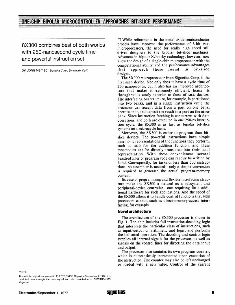
8X300 combines best of both worlds with 250-nanosecond cycle time and powerful instruction set
by John Nemec, Signetics Corp., Sunnyvale, Calif.
'NOTE
This article originally appeared in ELECTRONICS Magazine September 1,1977. It is reprinted here through the courtesy of and with permission of ELECTRONICS Magazine.
o While refinements in the metal-oxide-semiconductor process have improved the performance of 8-bit MOS
microprocessors, the need for really high speed still drives designers to the bipolar bit-slice machines. Advances in bipolar Schottky technology, however, now allow the design of a single-chip microprocessor with the computational ability and the performance advantages that approach those found in bit-slice designs.
The 8X300 microprocessor from Signetics Corp. is the first such device. Not only does it have a cycle time of 250 nanoseconds, but it also has an improved architecture that makes it extremely efficient; hence its throughput is vastly superior to those of MOS devices. The interfacing bus structure, for example, is partitioned into two banks, and in a single instruction cycle the processor can accept data from a port on one bank, operate on it, and deposit the result in a port on the other bank. Since instruction fetching is concurrent with data operations, and both are executed in one 250-ns instruction cycle, the 8X300 is as fast as bipolar bit-slice systems on a microcycle basis.
Moreover, the 8X300 is easier to program than bitslice devices. The powerful instructions have simple mnemonic representations of the functions they perform, such as ADD for the addition function, and these mnemonics can be directly translated into their octal representation. With these conveniences, several hundred lines of program code can readily be written by hand. Consequently, for tasks of less than 500 instructions, no assembler is needed -only a simple conversion is required to generate the actual program-memory content.
Its ease of programming and flexible interfacing structure make the 8X300 a natural as a subsystem and peripheral-device controller-one requiring little additional hardware for such applications. And the speed of the 8X300 allows it to handle control functions that MOS
processors cannot, such as direct-memory-access interfacing, for example.
Novel architecture
The architecture of the 8X300 processor is shown in Fig. I. The chip includes full instruction-decoding logic that interprets the particular class of instructions, such as input/output or arithmetic and logic, and performs the indicated operation. The decoding and control logic supplies all internal signals for the processor, as well as signals on the control lines for directing the data input and output.
The processor also contains its own program counter, which is automatically incremented upon execution of the instruction. The counter may also be left unchanged or loaded with a new value, Control of the current
Electronics/September 1, 1977 9!!1DDliC9 9
10
I I I L ____ -,
I
Ao-A'2 INSTRUCTION ADDRESS
OVERFLOW REGISTER
SHIFT
10-1'5 INSTRUCTION DATA
MERGE
INTERNAL CONTROL SIGNALS
DECODE AND
COUNTER LOGIC
.... 111111. IVBo-IVB7
" INTERFACE-VECTOR BUS
RIGHT BANK ) LEFT BANK DATA I/O WRITE CONTROL CONTROL SELECT CONTROL LINES
MASTER CLOCK HALT RESET
X2 } CRYSTAL
Xl
1. High-performance microcontroller. The Signetics 8X300 processor, a bipolar Schottky device with a 250-ns cycle time, is capable of
processing at throughputs rivaling those of bit-slice machines. Fetching of its 16-bit instructions is concurrent with data operations; and with a
bus partitioned into right and left banks, the 8X300 can, in a single instruction cycle, accept data, operate on it, and deposit the result.
address is provided by the address register and may be derived completely or partially from the program counter, from the instruction data lines (ARo through AR4),
or from the output of the arithmetic/logic unit (lines ARs through AR 12). Because of this flexible instructionaddress scheme, the order of execution may be altered by instructions or under conditions determined from selected data.
The read/write registers
The processor manipulates 8-bit data bytes. Internal data is stored in eight 8-bit read/write registers- R, through R 6, R II, and an auxiliary register. The auxiliary register holds one of the operands used in two-operand instructions, such as ADD or AND, and a single-bit overflow register stores the carry-over bit from additional operations.
Further, the addition of the rotate, mask, shift, and
merge functions to the ALU extends the 8X300's operating capability and enhances its efficiency.
Interfacing with external circuitry is through an 8-bit bus called the interface-vector bus and consisting of lines IV 0 through IV 7. The bus carries both address and data information, and the accompanying data-llo control lines tell the external circuitry which of the two types of information is on the bus. These lines include write- and select-control, right- and left-bank-signal, and masterclock lines.
Since the interface-vector bus carries addresses as well as data, I/O ports on the external circuits must be enabled before data transfer can take place. This is usually accomplished by placing an address on the bus under program control and then activating the selectcontrol line, which indicates that a valid address is on the bus. When presented with an address, each of the possible 512 1/0 ports either enables itself upon
SmnOliCS Electronics/September 1,1977
PROGRAM STORAGE
ROM, PROM, or RAM TTL-COMPATIBLE
UP TO 8 k x 16 BITS
5V
RESET----'
WORKING STORAGE.
'(RAM)
· · ·
8T32 DUAL-PORT REGISTER
TO EXTERNAL DEVICE
-'"---- BYTE INPUT CONTROL 1....-.---- BYTE OUTPUT CONTROL
TO eXTERNAL DEVICE
'-----ByTE INPUT CONTROL '------ BYTE OUTPUT CONTROL
2. System design. A typical configuration has memory for program storage and latches for up to 512 directly addressed 1/0 ports, which are
divided among left and right banks. All addresses and data are carried by the interface-vector bus and directed by control lines.
identifying the address as its own or disables itself if the addresses do not match.
The processor can directly address all of the 1/0 ports without the need for a decoder. The bus, and the interface-vector bytes on it, are bidirectional.
Within the processor, the interface-vector bytes are addressed in a unique fashion. Each 'byte has an 8-bit field-programmable address. When a given address is selected, the byte is automatically designated, and the 8X300 can then communicate with the '110 device. Moreover, once enabled, the addresses remain so until the processor changes them. This direct-addressing feature is especially convenient if a few ports are to be acc~ssed frequently. However, if the time required for this opera .. tion is an imposition on the user, instruction memory can be extended so that the selection of ports is automatic upon instruction fetch.
In extending the memory, an extra field is appended to each instruction through an additional bus ~ppFed to each 110 port. The address field may be as wide as required to serve all system 110 ports and, if necessary, to serve memory. The address field contains two addresses, since the interface-vector bus is partitioned into right and left banks.
Partitioning of the interface-vector bus into two banks allows the 8X300 to select ports dynamically. The
processor uses the left-bank (LB) and right-bank (RB) data-control lines as master enables for the 1/0 ports, as shown in the typical interconnect scheme of Fig. 2. Any two 110 ports can be active at the same time provided they are' on opposite banks, and th~ ports recognize address, data, and controls only when enabled by the bank signal to which each is connected. Bank partitioning can thus be considered a ninth addre&s bit that is alterable by the processor within an instruction, and it is this additional bit that permits direct addressing of 512, or 29, 110 ports.
In a general data operation between two 1/0 ports, first an address is presented to one bank that enables an 110 port and disables all others on the bank. Next, another address is presented to the opposite bank, effecting a similar selection there. Then the operation between the two takes place.
Instruction cycle
Each 8X300 operation is executed in one instruction cycle, which is s~bdivided into four quarter cycles as shown in Fig. 3. The instruction address for an operation is presented at the output of the processor during the third quarter of the previous instruction cycle. If the system memory is fast enough, the instruction returns to the processor during the first quarter of the cycle in
Electronics/September 1, 1977 SmlDliCS 11
INPUT PHASE OUTPUT PHASE , 1\ , I 1\ ,
MCLK = HIGH MCLK = LOW
INST AND DATA ADDR AND ADDR AND IV BUS PROCESSING IV BUS' IV BUS
DATA INPUT CHANGING DATA VALID
1+-% CyCLE ..... -+-% CYCLE-- 1+-% CyCLE .... -+-% CYCLF-.
L~ X 14 250 ns ~I
INST = INSTRUCTION IV = INTERFACE·VECTOR MCLK = MASTER CLOCK RB = RIGHT BANK LB = LEFT BANK
3. Instruction cycle. Two 1/0 ports may be dynamically selected in a single cycle if they are on opposite banks. Complementary LS and RS control signals change state during first and third quarter-cycles to accept data from one port and deposit it in the other.
which it is to be executed. The decoded instruction then directs the operation of the processor throughout the cycle.
In terms of processing data, the instruction cycle may be viewed as having two halves, an input and an output phase. During the first half of the instruction cycle, data is brought into the processor and stored in an interfacevector latch. Storage is completed during the first quarter cycle, and in the next quarter cycle the data is processed through the ALU. In the second half cycle, the data is presented to the bus and finally clocked into the designated 110 port.
Bank selection during the input and output phases is independent. Thus data may be received from the right bank, processed, and then deposited in the left bank or vice versa, or may even be sent to and from the same bank. Bank selection during instruction cycles is speci~ fied by the instruction.
Much of the strength of the 8X300 architecture lies in the powerful instruction set that controls the processor. The instruction words, each 16 bits in length, are made up of several fields that include the operational code, the source and destination fields, and the length field.
Instruction fields The contents of each field can be represented by a set
of octal digits, to simplify the task of coding. These digits have a direct relation to the specific operations that the data undergoes in its travel along the 8X300's internal data paths. The op code for addition, for example, is 0 I. In an operation between two I/O ports, the first of the source field's two digits specifies the bank and the second prescribes the number of bits to be rotated to the right. Similarly, the first digit of the destination field again specifies a bank, while the second digit prescribes the number of bits to be shifted. The length field specifies the number of bits to be accepted for operation in the ALU.
The capabilities of the 8X300 are such that it can, with few additional devices, perform all the functions required of an intelligent terminal. Whereas a typical system of this kind is constructed from many small- or medium-scale-integrated circuits for the control portion
of the terminal-cathode-ray-tube display, dot-matrix graphics, keyboard data entry, and host or mass-storage interface-and a microprocessor for the intelligence portion-data manipulation and number crunching-the 8X300 performs most of both the control and intelligence functions. The result is a system with fewer parts and far more capabilities for the money.
Intelligent terminal
The 8X300-based intelligent terminal depicted in Fig. 4 consists of four major sections. First is the interface section, which implements the standard RS-232C interface with the host or main-data storage. The Signetics 2651 programmable communications interface performs the serial-parallel data interconversion for byte processing by the 8X300 and for display-refresh memory. The interface section includes a keyboard that is scanned by the processor for operator inputs.
The second major section comprises the video circuitry that generates all pixel, character, and line timing, as well as the composite video signal. This circuitry also supplies signals to the refresh-memory address counter for proper timing of character codes and attributesblinking, reverse video, and so on. Synchronization, blanking, video, and attribute signals are then summed in the video mixer to produce the signal for driving standard monitors.
The third section, the refresh memory, stores the characters to be displayed on the screen. Its characters are addressed under control of the video-generator circuitry. The circuitry also provides for timing and control to facilitate interleaved access to the memory by the 8X300 processor. Interleaving permits the processor to examine or modify the refresh memory without disturbing the on-screen display or the video-refresh process.
The processor's role
The final section is the processor, the terminal's intelligence center. It performs both the executive controlmanaging the other three sections-and the dataprocessing function required by the terminal.
Since the 8X300 controls the refresh memory and video-generator sections and thus provides the timing for each frame, all frame-related features, such as scrolling and command-scanning, can be easily implemented. But most important, the processor also performs all the data manipulations-the intelligence within the terminal. The processor may accept input data from the host or the keyboard and can then present the data in proper format by means of the CRT display. Information may be entered or modified by the user and then returned to the host after the essential data items have been extracted from the refresh-memory file. This process, tailored to the user's needs, may be accomplished fully by the 8X300 microprocessor in firmware.
The basic control program, including keyboard scan, RS-232C interface service, edit, scroll, cursor, and so forth, requires only 502 words of program storage. Thus the entire terminal 'can be coded with two 4,096-bit programmable read-only memories. The balance of parts for the entire terminal hardware include the 2651
12 Ii!lDOliCI Electronics/September 1, 1977
INTERFACE
BAUD RATE CONTROL
PROGRAMMABLE N._PCii·I.DAIliTIIA._ COMMUNICATIONS
INTERFACE
2651
SYSTEM CLOCK
DUALPORT
VIDEO GENERATOR
LINE SYNC --..... TIMING
COUNTERS FRAME SYNC
.......... -..._ ..... --BLANK
SYSTEM CONTROLS
COMPOSlTE VIDEO
~~~~lR~EiG~IS~TE~RjI"""~ ..... __ .... (IV-2) CHARACTER GENERATOR
2513 ROM
ATTRIBUTE CONTROLLER
KEYBOARD
8X300
16-k PROM PROGRAM STORAGE
PROCESSOR
ERROR LED
SYSTEM TEST SIGNALS
MCLK SC WC RB LB
INTERFACE-VECTOR BYTES 1. MEMORY DATA 2. SYSTEM CONTROL 3. PROGRAMMABLE
COMMUNICATIONS INTERFACE DATA
4. PROGRAMMABLE COMMUNICATIONS INTERFACE CONTROL
REFRESH COUNTER
AND ADDRESS
LATCH
REFRESH MEMORY STATIC RAM
REFRESH MEMORY
4. Intelligent terminal. The 8X300 builds an intelligent terminal that, with a total of about only 40 devices, is low in cost while high in
capabilities. Included in the terminal are RS-232C interfacing, keyboard scanning, character generation with attributes, and fully interleaved refresh memory. The processor manages the other three sections and adds intelligence in data handling and number crunching.
programmable interface chip, the random-access memory for display refresh, a field-programmable logic array, and several low-power Schottky components, in addition to the 8X300. The use of about only 40 medium- and large-scale-integrated parts to construct the complete system contrasts with the over 110 smalland medium-scale-integrated components needed at present to build dumb terminals.
Floppy controlle~
The 8X3QO can be used in a very practical floppy-disk controller circuit that has few parts arid offers highly reliable control and data transfer and complete interfacing with the host processor. The processor's high speed enables it to handle any density-single, dual, and quad formats. With only minor firmware changes, a single hardware configuration can accommodate all popular disk drives and a variety of host processors.
What is more, it can do so within a single operating system-all that is needed is to switch from one set of firmware to another.
The floppy-disk controller, shown in Fig. 5, has basically two major functional parts, plus minor support functions. The two major sections are the processor and the control circuit.
The 8X300 communicates with the surrounding circuits through the interface-vector bus and controls the disk drives 'through command and status registers. Operating efficiency is high because selected' control and status bits share the same bidirectional I/O register, allowing both polling (status monitoring) and command to take place in as short a time as 250 ns. The processor's high speed allows simultaneous control of several disk drives for operations such as overlap seeks, where one drive is accessing while another reads or writes data. The 8X300's limits are reached only during tight-loop data
Electronics/September 1, 1977 9i!1DDliC9 13
~-----------------------~
PROGRAM MEMORY
I
I I I
COMMAND AND STATUS REGISTERS
1---- --. COMMAND
H------ STATUS
CYCLIC REDUNDANCY GENERATOR
CHECKER
WRITE PRECOMPENSATION
SECTOR LENGTH
COUNTER
READ PHASE-LOCKED' DATA
lOOP DATA SEPARATOR
t-_____ .. WRITE DATA
I I L flOPPY CONTROL CIRCUIT
HOST DATA BUS
_____ ~ ___ ~~~~ __ ~_~_~ __ J
WORKING STORAGE
5. Floppy-disk controller. High performance of the 8X300 allows it to effectively control a floppy-disk drive. The processor not only handles track and sector addressing but actually oversees data transfer. It also provides interfacing with the working store or directly with the host.
transfers that have to be extremely fast, but since these periods are very short, they present no significant system delays.
The 8X300 builds reliability into the disk operations by overseeing the actual data transfer, in ~ddition to positioning the read/write head. The intelligence of the processor can be used to reread data after it has been written or even to mask out bad tracks that fail to read correctlyafter, say, 10 rewrites.
E"icient operation
Registers within the 8X300 monitor the track and sector addresses, making seeks and sector accesses highly efficient. In setting up the data transfers, the 8X300 monitors both interleaved data on the disk and the system clock for address-mark detection; it then exam .. ines a,nd moves data a byte at a time once the controller circuit has been synchronized with the byte boundaries. Under control of the processor, disk data may be trans· (erred to working storage (which can interface directly with the processor bus) for subsequent. transfer to the host or, if it can be accommodated, transferred immediately to the host.
Very little external logic is needed for direct-memoryaccess interfacing between the 8X300 and the host. Transfer of data, commands, a~d status takes place
through eight bidirectional 1/0 ports that are compatible with transistor-transistor logic and are supplemented with additional logic for direct connection to the host. The protocol is established in processor microprogram. ming, which may be conveniently altered for a variety of host types. Total program size for disk control and interfacing the 8X300 with the host processor is less than 800 instructions.
The other major section, the control circuit, has the hardware, which does a better job of recovering data from the disk than microprocessor software could. Functions include phase-locked-loop data separation, cyclic redundancy generating and checking, data-byte assem" bly and disassembly, and precompensation for widening the write pulses applied to the disk. These circuit functions, under control of the 8X300, can easily be instructed to operate for either single or dual recording densities, and the system can be expanded to handle most types of quad-density encoding.
Counting the control circuit as two LSI devices, the entire floppy-disk controller can be built from about 12 components. The system is complete in that it not only controls the access of disk data, but also provides the interface between any host and any off-the-shelf floppy .. disk drive, and monitors and checks data transfer for ultimate reliability. 0
14 Si!lIOliCS Electronics/September 1, 1977
MICROCONTROLLER
DESCRIPTION
The Signetics 8X300 Microcontroller is a monolithic, high-speed microprocessor implemented with bipolar Schottky technology. As the central processing unit, CPU, it allows 16-bit instructions to be fetched, decoded and executed in 250ns. A 250ns instruction cycle requires maximum memory access of 65ns, and maximum I/O device access of 35ns.
Microcontroller instructions operate on 8 .. bit, parallel data. Logic is distributed along the data path within the Microcontroller. Input data can be rotated and masked before being subject to an arithmetic or logicar operation; and output data can be shifted and merged with the input data, before being output to external logic. This allows 1-to 8-bit I/O and data memory fields to be accessed and processed in a Single instruction cycle.
PROGRAM STORAGE INTERFACE Program Storage is typically connected to the AO-A 12 (A 12 is least significant bit) and 10-115 signal lines. An address output on AO-A 12 identifies one 16-bit instruction word in program storage. The instruction word is subsequently input on 10-/15 and defines the M icrocontroller operations which are to follow.
The Signetics 82S115 PROM, or any TTL compatible memory, may be used for program storage.
I/O DEVICES INTERFACE An 8-bit I/O bus, called the Interface Vector (IV) data bus, is used by the Microcontroller to communicate with 2 fields of 1/0 devices. The complementary LB and RB signals identify which field of the I/O devices is selected.
Both I/O data and I/O address information can be output on the IV bus. The SC and WC signals are typically used to distinguish between 1/0 data and I/O address information as follows:
se we 1 0 I/O address is being output on IV
bus o 1 1/0 data is being output on IV bus o 0 1/0 data is expected on the IV,
bus, as input to the Microcontroller 1 1 Not generated by the Microcontrol
ler
The Signetics 82SXXX series RAM, and the 8T32/33 may be attached to the IV bus.
FEATURES PIN CONFIGURATION
• 185ns instruction decode and execute delay (with Signetics 8T32/33 1/0 port) VCR
IZA PACKAGE 50
• Eight 8-bit working registers A7 A6 A5 A4 A3 A2 At. AO Xl X2
• Single instruction access to 1-bit, 2-blt, 3· bit or 8-bit field on 1/0 bus
• Separate Instruction address, instruc· tion, and 1/0 data buses
• On-chip oscillator • Bipolar Schottky technology GND
10 11 12 13 14 15
16 17 18 19
• TTL inputs and outputs • Tri-state output on 1/0 data bus • +5 volt operation from 0° to 70° C
PIN DESIGNATION
PIN SYMBOL
2-9,45-49 AO-A12:
13-28 10-/15:
33-36, IVBO-IVB7 38-41
42 MCLK:
30 we:
29 SC:
31 LB:
32 RB:
44 HALT: ---
43 RESET:
10-11 X1, X2:
50 VR
1 VCR
37 Vce:
12 GND:
9!!JDOliC9
110 111 112 25 26
NAME AND FUNCTION
Instruction address lines. A high level equals "1." These outputs directly address up to 8192 words of program storage. A12 is least significant bit.
Instruction lines. A high lever equals "1." Receives instructions from Program Storage. ' 15 is least significant bit.
Interface Vector (IV) Bus. A low level equals "1." Bidirectional tri-state lines to communi-cate with 1/0 devices.IVB7 is least significant bit.
Master Clock. Output to clock 1(0 devices, andlor provide synchronization for external logic
Write Command. High level output indicates data is being output on the IV Bus.
Select Command. High level output indicates that an address is being output on the IV Bus.
Left Bank. Low level output to enabre one of two sets of 110 devices (LB is the comple-ment of RS).
Right Bank. Low level output to enable one of two sets.!!! I/O devices (RB is the comple-ment of LS).
Low level is input to stop the Microcontroller.
Low level is input to initialize the Mlcrocon-troller. Inputs for an external frequency determining crystal. May also be interfaced to logic or test equipment.
Reference voltage to pass transistor.
Regulated output voltage from pass transistor.
5V power connection.
Ground.
8X300
VR A8 A9
Al0 All A12 HAL:T REsET MCLK "iVBO ~ iVB2 iVB3 vcc 'iVs4 Ti7B5 iVB6 iVs7 RB LB wc SC 115 114 113
TYPE
Active high
Active high
Three-state Active low
Active high
Active high
Active high
Active low
Active low
Actfve low
Active low
15
4MICROGONIROLLER
V ....
~ f--I'.. ALU
~K ....
L __ (S}=O 'I
I I I I I I ARO-AR4
AR5-AR12 I
1 1 I
L_
0 12
AR
~ll AO-A12
INSTRUCTION ADDRESS
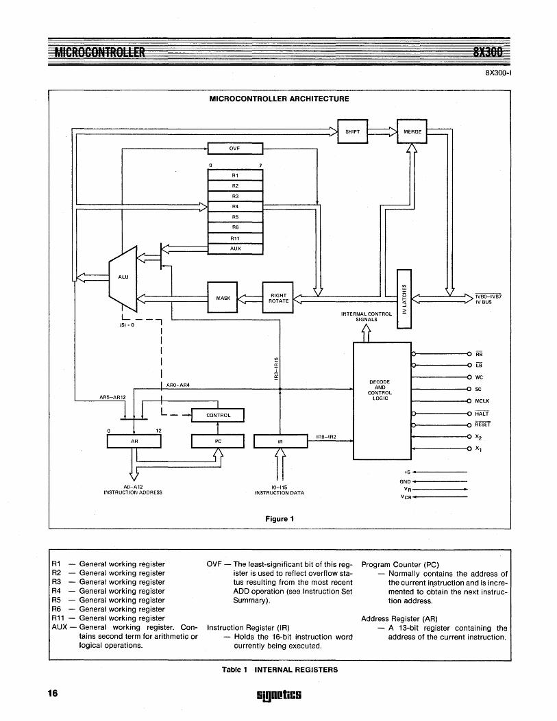
R1 - General working register R2 - General working register R3 - General working register R4 - General working register R5 - General working register R6 - General working register R11 - General working register
I
AUX - General working register. Contains second term for arithmetic or logical operations.
16
MICROCONTROLLER ARCHITECTURE
.. I I _ .... I -1 SHIFT r .".)f MERGE t--r
I OVF I 1\ I I
0 7
R1
R2
R3 .. ......, R4 ... R5
R6
R11
AUX
..--
en ~ UJ
V'-- RIGHT :r
~
MASK L-.- (..)
ROTATE I-"I ... «
-l
INTERNAL CONTROL :! SIGNALS
{r l....-
~
v ~
~ a: ..., I M
£!: DECODE
AND CONTROL
LOGIC
I ~
'7 ~ ..
:>
~
"" ,..
-..., 1"\ ...,
,..
,..
8X300 8X300-1
IVBO-IVB7 IV BUS
LB
WC
SC
MCLK
CONTROL I v -t
I I I IRO-IR2 PC IR I {r /1
10-115 INSTRUCTION DATA
Figure 1
OVF - The least-significant bit of this register is used to reflect overflow status resulting from the most recent ADD operation (see Instruction Set Summary).
Instruction Register (IR) - Holds the 16-bit instruction word
currently being executed.
Table 1 INTERNAL REGISTERS
SmnOliC!i
..., ..., ,.. --...,
+5 •
GND •
VR------
VCR .. ·------
Program Counter (PC) - Normally contains the address of
the current in..struction and is incremented to obtain the next instruction address.
Address Register (AR) - A 13-bit register containing the
address of the current instruction.
, j
INSTRUCTION CYCLE Each Microcontroller operation is executed in 1 instruction cycle, which may be as short as 250ns. The Microcontroller generates MCLK to synchronize external logic to the instruction cycle. Instruction cycles are subdivided into quarter cycles. MCLK is an output during the last quarter cycle.
During the third quarter cycle of an instruction, an address is output on AO-A 12, identifying the location in program storage of the next instruction word. This instruction word defines the next instruction, which must be input on 10-115 during the first quarter cycle of the next instruction cycle (see Table 2).
Instruction Set Summary The 16-bit instruction word input on 10-115 is decoded by the instruction decode logic to implement events that are to occur during the remainder of the instruction cycle. Generally the 16-bit instruction word is decoded as follows:
Bit POlition 0 1 2 3 15
I '--v---'
Inltruction Operand(l) Specification Cia ..
A detailed usage of the 13 "operand(s) specification" bits is given in following sections.
Three operation code bits allow for 8 instruction classes. The 8 instruction classes are summarized in Table 3. Each entry is referred to as an "instruction class" because the unique architecture of the Interpreter allows a number of powerful variations to be specified by the 13 operand (s) specification bits. A complete description of instruction formats and some instruction examples are provided in the Microprocessor Applications manual.
Data Processing The Microcontroller architecture includes eight 8-bit working registers, an arithmetic logic unit (ALu), an overflow register, and the 8-bit IV Bus. Internal 8-bit data paths connect the registers and IV Bus to the ALU inputs, and the ALU output to the registers and IV Bus. Data processing logic is distributed along these internal 8-bit data paths. Rotate and mask logic precedes the ALU on the data entry path. Shift and merge logic follows the ALU on the data output path. All 4 sets of logic can operate on 8 data bits in a Single instruction cycle (See Figure 1).
When less than 8 bits of data are specified for output to the IV bus by the ALU, the data field (shifted if necessary) is inserted into the prior contents of the IV bus latches. The
8X300-1
TYPICAL SYSTEM CONFIGURATION
+5V
~ •
..J:-U·~ ...
~u, ~
PROGRAM STORAGE
• • • ~
..
USER CONNECTION
A AO-A12 VCC VR VCR .A~ .~ 8T32
r--~
10-115 '1
SC r--ROM/PROM/RAM
~ WC ~
TTL COMPATIBLE r 8X300 MCLK UP TO BK x 16 BITS MICRO- LB tt Xl
(B2S115) CONTROLLER RB ..c--
n ~ B.O D MHZ~
.. X2
RAL'f----1 1 1 !'. BT33
~ REsEi' GND ~
f1 ""'I:",,!r
• BOC • Figure 2
INSTRUCTION ADDRESS AND AND IV ADDRESS IV BUS DATA
BUS DATA DATA AND IV VALID INPUT PROCESSING BUS CHANGING MCLK=HIGH
4- 1/4 cycle -- -1f4 cycle- -V4cycle- -V4cycle-
Table 2 INSTRUCTION CYCLE
IV bus latches contain data input at the start of an instruction. This data in the IV bus latches will be specified in the instruction as a) IV bus source data or b) data from an automatic read when the IV bus is specified as a destination. Therefore, IV bus bit positions outside an inserted bit field are unmodified.
Data Addressing Sources and destinations of data are specified using a 5-bit octal number. The source and/or destination of data to be operated upon is specified in a Single instruction word.
Referring to Figure 1, the Auxiliary register (address 00) is the implied source of the second argument for ADD, AND or XOR operations.
IVL and IVR are write-only registers used only as a destination. They have addresses and are treated as registers, but in reality they do not exist. When IVL is specified as a destination or the 0 field = 20-278, then LB = 'low', RB = 'high' are generated; when IVR is specified as a destination or the 0 field = 30-378, then RB = low, LB = 'high' are generated.
When IVL or IVR is specified as the destination in an instruction, SC is also activated
!ii!lDOliC!i
and data is placed on the IV bus. If IVL or IVR is specified as a source of data, the source data is all zeroes.
INSTRUCTION SEQUENCE CONTROL The Address Register and Program Counter are used to generate addresses for accessing an instruction. The Address Register is used to form the instruction address, and in all but 3 instructions (XEC, NZT, and JMP) the address is copied into the Program Counter. The instruction address is formed in 1 of 3 ways:
1. For all instructions but the JMP, XEC, and a satisfied NZT, the Program Counter is incremented by 1 and placed in the Address Register.
2. For the JMP instruction, the full 13-bit address field from the JMP instruction is placed into the Address Register and copied into the Program Counter.
3. For the XEC and NZT instructions, the high order 5- or 8-bits of the Program Counter are combined with 8- or 5-lower-order bits of ALU output (XEC or NZT) and placed in the Address Register. For the NZT instruction, it is also copied into the Program Counter.
17
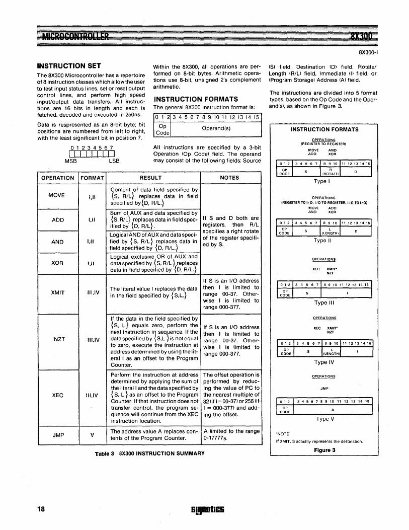
INSTRUCTION SET Within the aX300, all operations are performed on a-bit bytes. Arithmetic operations use a-bit, unsigned 2's complement arithmetic.
The aX300 Microcontroller has a repertoire of a instruction classes which allow the user to test input status lines, set or reset output control lines, and perform high speed input/output data transfers. All instructions are 16 bits in length and each is fetched, decoded and executed in 250ns.
INSTRUCTION FORMATS The general aX300 instruction format is:
o 1 2 3 4 5 6 7 a 9 10 11 12 13 14 15 Data is respresented as an a-bit byte; bit positions are numbered from left to right, with the least significant bit in position 7.
Op Operand(s) Code
01234567 I I I I I I I I I
MSB LSB
All instructions are specified by a 3-bit Operation (Op Code) field. The operand may consist of the following fieldS: Source
OPERATION FORMAT RESULT NOTES
MOVE
ADD
AND
XOR
XMIT
NZT
XEC
JMP
18
f,1I
I,ll
I,ll
I,ll
1I1,IV
III,IV
III,IV
v
Content of data field specified by {S, R/L} replaces data in field specified bY{D, R/L.}
Sum of AUX and data specified by {S, R/L} replaces data in field spec-ified by {D, R/L}.
Logical AND of AUX and data speci-fied by {S, R/L} replaces data in field specified by {D, R/L.}
Logical exclusive OR of AUX and data specified by { S, R/L} replaces data in field specified by {D, R/L.}
The literal value I replaces the data in the field specified by {S,L.}
If the data in the field specified by {S, L} equals zero, perform the next instruction in sequence. If the data specified by { S,L } is not equal to zero, execute the instruction at address determined by using the literal I as an offset to the Program Counter.
Perform the instruction at address determined by applying the sum of the literal I and the data specified by { s, L } as an offset to the Program Counter. If that instruction does not transfer control, the program sequence will continue from the XEC instruction location.
If Sand 0 both are reg isters, then R/L specifies a right rotate of the register specified by S.
If S is an I/O address then I is limited to range 00-37. Otherwise I is limited to range 000-377.
If S is an 1/0 address then 1 is limited to range 00-37. Otherwise I is limited to range 000-377.
The offset operation is performed by reducing the value of PC to the nearest multiple of 32 (if I = 00-37) or 256 (if· I = 000-377) and adding the offset.
The address value A replaces con- A limited to the range tents of the Program Counter. 0-177778.
Table 3 8X300 INSTRUCTION SUMMARY
SmOlltiC9
11311 ,
aX300-1
(S) field, Destination (D) field, Rotate! Length (R/L> field, Immediate (I) field, or (Program Storage) Address (A) field.
The instructions are divided into 5 format types, based on the Op Code and the Operand(s), as shown in Figure 3.
INSTRUCTION FORMATS
OPERATIONS lREGISTER TO REGISTER)
MOVE AND ADD XOR
Type I
OPERATIONS
{REGISTER TO lID. 1/0 TO REGISTER. lID TO 110)
MOVE ADD AND XOR
Type II
OPERATIONS
XEC XMIT' NZT
8 9 10 11 12 13 1415
Type III
OPERATIONS
XEe XMIT' NZT
Type IV
OPERATIONS
JMP
3 4 5 6 7 8 9 10 11 12 13 14 15
A
Type V
'NOTE
If XMIT. S actually represents the destination.
Figure 3
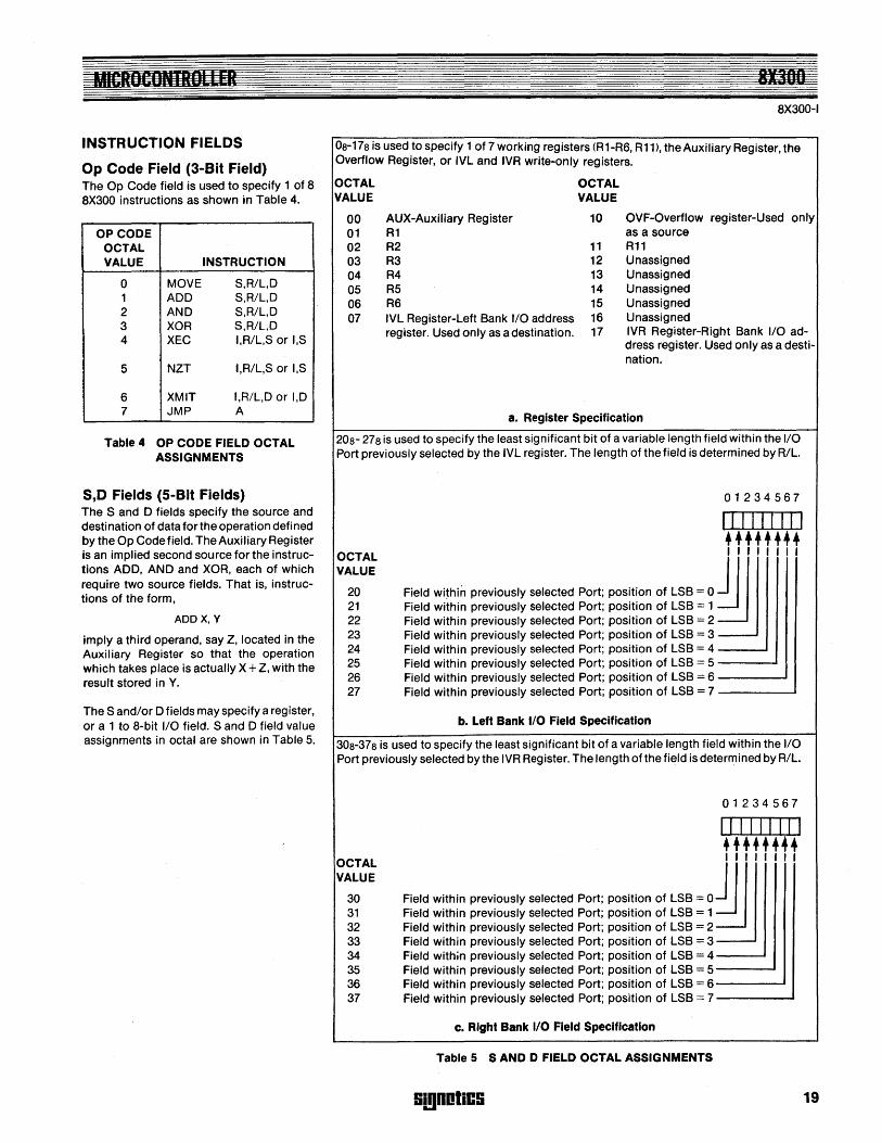
INSTRUCTION FIELDS
Op Code Field (3-Bit Field) The Op Code field is used to specify 1 of a aX300 instructions as shown in Table 4.
OP CODE OCTAL VALUE INSTRUCTION
0 MOVE S,R/L,D 1 ADD S,R/L,D 2 AND S,R/L,D 3 XOR S,R/L,D 4 XEC I,R/L,S or I,S
5 NZT I,R/L,S or I,S
6 XMIT I,R/L,D or I,D 7 JMP A
Table 4 OP CODE FIELD OCTAL ASSIGNMENTS
S,D Fields (5-Bit Fields) The Sand D fields specify the source and destination of data for the operation defined by the Op Code field. The Auxiliary Register is an implied second source for the instructions ADD, AND and XOR, each of which require two source fields. That is, instructions of the form,
ADD X. Y
imply a third operand, say Z, located in the Auxiliary Register so that the operation which takes place is actually X + Z, with the result stored in Y.
The Sand/or D fields may specify a register, or a 1 to a-bit I/O field. Sand D field value assignments in octal are shown in Table 5.
aX300-1
08-178 is used .to specify 1 of 7 working registers (R1-R6, R11), the Auxiliary Register, the Overflow Register, or IVL and IVR write-only registers.
OCTAL OCTAL VALUE VALUE
00 01 02 03 04 05 06 07
AUX-Auxiliary Register 10 R1
OVF-Overflow register-Used only as a source
R2 11 R11 R3 12 Unassigned R4 13 Unassigned R5 14 Unassigned R6 15 Unassigned
Unassigned IVL Register-Left Bank I/O address 16 register. Used only as a destination. 17 IVR Register-Right Bank I/O ad
dress register. Used only as a destination.
a. Register Specification
208- 278 is used to specify the least significant bit of a variable length field within the I/O Port previously selected by the IVL register. The length of the field is determined by R/L.
OCTAL VALUE
20 21 22 23 24 25 26 27
01234567
111111111 •••••••• 11111111
Field wi!hin previously selected Port; position of LSB ~ 0 J 'II Field within previously selected Port; position of LSB = 1 :J Field within previously selected Port; position of LSB = 2 Field within previously selected Port; position of LSB = 3 Field within previously selected Port; position of LSB = 4 ------' Field within previously selected Port; position of LSB = 5 ---....I Field within previously selected Port; position of LSB = 6 ----..I Field within previously selected Port; position of LSB = 7 -------'
b. Left Bank I/O Field SpeCification
308-378 is used to specify the least significant bit of a variable length field within the I/O Port previously selected by the IVR Register. The length of the field is determined by R/L.
OCTAL VALUE
30 31 32 33 34 35 36 37
01234567
111111111 •••••••• I I I I I I I I
Field within previously selected Port; position of LSB ~ oj 'II Field within previously selected Port; position of LSB = 1 :J Field within previously selected Port; position of LSB = 2 Field within previously selected Port; position of LSB = 3 Field within previously selected Port; position of LSB = 4 -----' Field within previously selected Port; position of LSB = 5 ___ ...J
Field within previously selected Port; position of LSB = 6 ----..I Field within previously selected Port; position of LSB = 7 --------'
c. Right Bank I/O Field Specification
Table 5 SAND D FIELD OCTAL ASSIGNMENTS
S!!IDDliCS 19
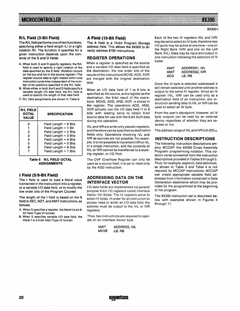
MICROCONTROLLER
R/L Field (3-Bit Field) The R/L field performs one of two functions, specifying either a field length (U or a right rotation (R). The function it specifies for a given instruction depends upon the contents of the Sand 0 fields:
A. When both Sand 0 specify registers, the R/L field is used to specify a right rotation of the data specified by the S field. (Rotation occurs on the bus and not in the source register.) The register source data is right rotated within one instruction cycle time independent of the number of bit positions specified in the R/L field.
B. When either or both the Sand 0 fields specify a variable length 1/0 data field, the R/L field is used to specify the length of that data field.
C. R/L field assignments are shown in Table 6.
R/L FIELD OCTAL SPECIFICATION VALUE
0 Field Length = 8 Bits 1 Field Length = 1 Bit 2 Field Length = 2 Bits 3 Field Length = 3 Bits 4 Field Length = 4 Bits 5 Field Length = 5 Bits 6 Field Length = 6 Bits 7 Field Length = 7 Bits
Table 6 R/L FIELD OCTAL ASSIGNMENTS
I Field (5/8-Bit Field) The I field is used to load a literal value (contained in the instruction) into a register, or a variable I/O data field, or to modify the low order bits of the Program Counter.
The length of the I field is based on the S field in XEC, NZT, and XMIT instructions, as follows: A. When S specifies a register, the literal I is an 8-
bit fieid (Type III format). B. When S specifies variable 1/0 data field, the
literal I is a 5-bit field (Type IV format).
20
A Field (13-Bit Field) The A field is a 13-bit Program Storage address field. This allows the 8X300 to directly address 8192 instructions.
REGISTER OPERATIONS When a register is specified as the source and a variable I/O data field is specified as the destination, the low order bits of the results of the instructions MOVE, ADD, XOR are merged with the original destination data.
When an I/O data field of 1 to a bits is specified as the source, and a register as the destination, the a-bit result of the operations MOVE, ADD, AND, XOR is stored in the register. The operations ADD, AND, XOR actually use the I/O data field (1 to 8 bits) with leading zeros to obtain a-bit source data for use with the 8-bit AUX data during the operation.
IVL and IVR are write-only pseudo registers, and therefore can be specified as destination fields only. Operations involving IVL and IVR as sources are not possible. For example, it is not possible to increment IVR or IVL in a single instruction, and the contents of IVL or IVR cannot be transferred to a working register, or I/O Port.
The OVF (Overflow) Register can only be used as a source field; it is set or reset only by the ADD instruction.
ADDRESSING DATA ON THE INTERFACE VECTOR I/O data fields are implemented via general purpose a-bit I/O registers called Interface Vector (IV) Bytes. The IV registers serve to select IV bytes. In order for an instruction to access (read or write) an I/O data field, the address must be output to the IVL or IVR registers.
Thus, two instructions are required to operate on an Interface Vector byte.
XMIT MOVE
ADDRESS, IVL LB,RB
!ii!lDOliC9
8X30o
8X300-1
Each of the two IV registers (IVL and IVR) may be set to select an IV byte, therefore two I/O ports may be active at one time-one on the Right Bank (IVR) and one on the Left Bank (lVU. Data may be input and output in one instruction following the selection of IV bytes:
XMIT ADDRESS1,IVL XMIT ADDRESS2, IVR ADD LB, RB
Once the IV byte is selected (addressed) it will remain selected until another address is output to the same IV register. Since an IV register (lVL, IVR) can be used only as a destination field of an instruction, any instruction sending data to IVL or IVR can be used to select an IV byte.
From the user's standpoint, however, all IV byte outputs can be read by an external device regardless of whether they are selected or not.
The address range of IVL and IVR is 0-25510.
INSTRUCTION DESCRIPTIONS The following instruction descriptions employ MCCAP (the 8X300 Cross Assembly Program) programming notation. This notation varies somewhat from the instruction descriptions provided in Tables 3 through 5. Thus, for example, explicit L field definition, as shown in Table 3 and Table 4 is not required by MCCAP instructions; MCCAP can create appropriate variable field addresses from information contained in Data Declaration statements which may be provided by the programmed at the beginning of his program.
The 8X300 instruction set is described below with examples shown in Figures 4 through 11.
MICROCONTROELER
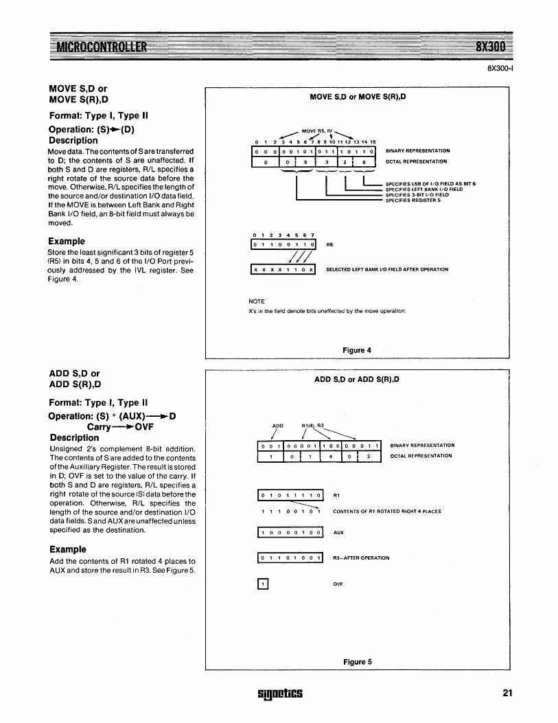
MOVE S,D or MOVE S(R),D
Format: Type I, Type II
Operation: (S)+--(D) Description Move data. The contents of S are transferred to D; the contents of S are unaffected. If both Sand D are registers, R/L specifies a right rotate of the source data before the move. Otherwise, R/L specifies the length of the source andlor destination 1/0 data field. If the MOVE is between Left Bank and Right Bank I/O field, an 8-bit field must always be moved.
Example Store the least significant 3 bits of register S (RS) in bits 4, Sand 6 of the 1/0 Port previously addressed by the IVL register. See Figure 4.
ADD S,D or ADD S(R),D
Format: Type I, Type II
Operation: (S) + (AUX)--.D CarrY--'OVF
Description Unsigned 2's complement 8-bit addition. The contents of S are added to the contents of the Auxiliary Reg ister. The resu It is stored in D; OVF is set to the value of the carry. If both Sand D are registers, R/L specifies a right rotate of the source (S) data before the operation. Otherwise, R/L specifies the length of the source andlor destination 1/0 data fields. Sand AUX are unaffected unless specified as the destination.
Example Add the contents of R1 rotated 4 places to AUX and store the result in R3. See Figure S.
MOVE S,D or MOVE S(R),D
BINARY REPRESENTATION
OCTAL REPRESENTATION
'-.-" ------L SPECIFIES LSB OF 1/0 FIELD AS BIT 6
..... ___ SPECIFIES LEFT BANK 1/0 FIELD
L __ -======= ~:~g:~:~~ ~~Bri~~~~RF~ELO 01234567
10 1 1 0 0 1 1 01 R5
III 1 x x x X 1 1 0 xl SELECTED LEFT BANK 110 FIELD AFTER OPERATION
NOTE
X's in the field denote bits unaffected by the move operation.
Figure 4
ADD S,D or ADD S(R),D
BINARY REPRESENTATION
OCTAL REPRESENTATION
10 1 0 1 1 1 1 0 I R1
cz:::::::: 1 1 1 0 0 1 0 1 CONTENTS OF R1 ROTATED RIGHT 4 PLACES
11 0 0 0 0 1 0 0 I AUX
1 0 1 1 0 1 0 0 1 I R3-AFTER OPERATION
OVF
Figure 5
!i!!JDDliC!i
8X300-1
21
AND S,D or AND S(R),D
Format: Type I, Type II Operation: (S) A (AUX)~D Description logical AND. The AND of the source field and the Auxiliary Register is stored into the destination. If both Sand D are registers, AIL specifies aright rotate of the source (S) data before the AND operation. Otherwise AIL specifies the length of the source and! or destination I/O data fields. Sand AUX are unaffected unless specified as a destination.
Example Store the AN D of the selected right bank 110 field and AUX in R4. The right bank data field is called WSBCD and IS 4 bits long and located in bits 2, 3, 4 and 5. See Figure 6.
XOR S,D or XOR S(R),D
Format: Type I, Type II Operation: (S) ffi (AUX) .. D Description Exclusive-OR. The Exclusive-OR of the source field and the Auxiliary Register is stored in the destination. If both Sand Dare registers, RIL specifies a right rotate of the source (S) data before the XOR operation. Otherwise R/L specifies the length of the source and/or destination I/O data fields. S and AUX are unaffected unless specified as a destination.
Example Replace the selected I/O data field with the XOR of the field and AUX. The I/O data field is called STATUS and is 5 bits in length and located in bits 3,4, 5, 6 and 7 of left bank. See Figure 7.
22
AND S,D or AND S(R),D
BINARY FlEPAESENfATtON
OCTAL AEPRESENTATtON
..... _- SPECIFIES REGISTER 4
l_...!:=~======= SPECIFIES 4-BIT 1/0 FIELD SPECIFIES LSB OF RB FIEL.D AS BIT 6 SPECIFIES RB FIELD
01234561
I, 0 0 1 0 1 0 1 1 SEL.ECTED RIGHT BANK 110 FIELD
~~ o 0 0 0 0 1 0 1 SELECTED FIELD RIGHT JUSTtFtED WITH lEADING ZEROS ADDED.
AND OPERATtON
10 0 0000111 AUX
l . I 0 0 0 0 0 0 0 1 I R4
Figure 6
XOR S,D or XOR S(R),D
81NARY REPRESENTATION
OCTAL REPRESENTATION
o 1 2 3 4 6 6 7
I 0 , 1 1 0 0 1 1 I SELECTED 110 DATA FIELD-BEFORE OPERATION
1 t ! l l o 0 0 1 0 0 1 1 SELECTED FIELD RIGHT JUSTIFIED WITH LEADING lEROS ADDED
XOR OPERATION
I 0 0 0 0 1 0 1 0 I AOX
00011001
l III , I 0 1 1 1 1 0 0 1 I SELECTED tlO-AFTER OPERATION -UNAFFECTED
Figure 7
SmnOliCS
8X300 .. '
MICROCONTROLLER
XEC I(S)
Format: Type III, Type IV
Operation Execute instruction at the address specified by the Address Reg ister with lower 5 or 8 bits replaced by (S) + I.
Description Execute the instruction at the address de~ termined by replacing the low order bits of the Address Register (AR) with the low order bits of the sum of the literal I and the contents of the source field. If S is a register, the low order 8 bits of AR are replaced; if S is an I/O data field, the low order 5 bits of AR are replaced, resulting in an execute range of 256 and 32 respectively. The Program Counter is not affected unless the instruc· tion executed is a JMP or NZT (whose branch is taken).
Example Execute one of n JMPs in a table of JMP instructions determined by the value of the selected I/O data field on the left bank. The table follows immediately after the XEC instruction and the I/O field is called INTERPT and is a 3-bit field located in bits 4,5 and 6. See Figure 8.
XMITI,D
Format: Type III, Type IV
Operation: I'" (0)
Description Transmit literal. The literal field I is stored in D. If 0 is a register, an 8-bit field is transferred; if D is an I/O data field, up to a 5-bit field is transferred.
Example Store the bit pattern 110 in the selected I/O data field on the right bank. The field name is VALUE and is located in bits 3, 4 and 5. See Figure 9.
XEC I(S)
o 13
BINARY REPRESENTATION
OCTAL REPRESENTATION
I 0 0 0 0 1 1 0 1 1 0 0 1 1 I ADDRESS REGISTER-·BEFORE OPfRATtON
012345117
10 1 0 1 0 1 1 0 I SELECTED 110 DATA FIELD
\\\ o 0 0 0 0 0 1 1 SELECTED FIELD RIGHT JUSTIFIED WITH LEADING ZEROS ADDEO
000 101 0 0 I FielD
00010111
I~C:;:I 0000110110111 ADDRESS REGISTER AFTER OPERA nON
-...-UNAFFECTED
ADDRESS
0000110110011 0000110110100
• • • 0000110110111
• • • 0000110111011
INSTRUCTION
XEC "1 (lNTERPTI JMPA1
JMPA4
JMPA8 I JMP A4 IS EXECUTED BECAUSE 110 FIELD INTERPT" 3
Figure 8
XMIT I,D
o 1 234 5 II 7
JMPTABI.E
BINARY REPRESENTATION
OCTAL REPRESENTATION
1 1 0 0 1 0 0 1 I SELECTED 110 DATA-BEFORE OPERATION
o 0 0 0 0 1 1 0 I FIELD
/// 1 1 0 1 1 0 0 1 I SELECTED 110 DATA-AFTER OPERATION
'.NAFFECTEDT
Figure 9
!i!!lDOliCS
81300 8X300-1
23
NZT S,I
Format: Type III, Type IV
Operation: Non-Zero Transfer. If (S) =I:- 0, PC offset by I .... PC; otherwise PC + 1 - PC.
Description If the data specified by the S field is nonzero, replace the low order bits of the Program Counter with I. Otherwise, processing continues with the next instruction in sequence. If S is a register, the low order 8 bits of the PC are replaced; if S is an 1/0 data field, the low order 5 bits of the PC are replaced, resulting in an NZT range of 256 and 32 respectively.
Example Jump to Program Address ALPHA if the selected left bank I/O field is non-zero. The field name is OVER FLO and it is a 1-bit field located in bit 3. See Figure 10.
JMPA
Format: Type V
Operation: A -- PC
Description The literal value A is placed in the Program Counter and Address Register, and processing continues at location A. A has a range of 0-177778 (0-8191),
Example Jump to location ALPHA (0000101110001), See Figure 11.
24
NZTS,I
BINARY REPRESENTATION
OCTAL REPRESENTATION
01234567
I x x x 1 X X X x I SELECTED I/O DATA
OVERFLO
• • • 0000110110011
• • • ALPHA 0000110111010
OFFSET
ALPHA
\
ADDRESS
• • • 6000000011 011
• • • ALPHA 0000101110001
INSTRUCTION
NZT OVER FLO. ALPHA
INSTRUCTION
Figure 10
JMPA
BINARY REPRESENTATION
OCTAL REPRESENTATION
INSTRUCTION
JMP ALPHA
INSTRUCTION
1 0 1 0 1 0 1 0 1 01 0 1 0 1 0 11 11 1 0 11 11 I PROGRAM COUNTER BEFORE OPERATION
1 0 1 0 101 0 11 1011 11 11 10 1 01 0 I 1 I PROGRAM COUNTER AFTER OPERATION
Figure 11
9i!100IiC!i
MICROCONTROLLER
SYSTEM DESIGN USING THE 8X300 MICROCONTROLLER Designing hardware around the 8X300 Interpreter reduces to selecting a program storage devicer (ROM, PROM, etc.)', selecting I/O devices (IV byte, multiplexers, RAM, etc.), selecting clock mode (system driven or crystal controlled) and interfacing the Microcontroller to these components.
A specific example of a control system using the 8X300 Microcontroller is shown in Figure 12. Only 8 components-four 8T32 I/O Ports, one 8X350 RAM, two 82S215 ROMs, and an 8X300 are required to build this system which contains 512 words of program storage, 32 TTL I/O connection points, 256 bytes of working storage, and operates at a 250ns instruction cycle time.
... A4-A12
~
SIGNETICS 82S215 512x8 ROM
110- 17
f--
A4-A12 CE1
Q CE2
STROBE
AO-A3
Halt, Reset Signals
HALT: A low level at the HALT input stops internal operation of the Microcontroller at the start of the next instruction after HALT is applied (quarter cycle after MCLK). Since HALT is sampled at the start of each instruction cycle it is possible to prevent a cycle by applying HALT early in that cycle. HALT does not inhibit MCLK or affect any internal registers. Normal operation begins with the next complete cycle after the HALT input goes high.
EXAMPLE OF CONTROL SYSTEM
+5V ~ ) 0 I)
t1~
'~ .1
VCC VR vCRT
~
* IVBO-IVB7
8X300 MICROCONTROllER MCLK,
SC,WC
81300 8X300-1
RESET: A low level at the RESET input sets the program counter and address register to zero. While RESET is low MCLK is inhibited. If RESET is applied during the last 2 quarter cycles, the MCLK during that cycle may be shortened. RESET should be applied for 1 full instruction cycle time to assure proper operation. When RESET input goes high an MCLK occurs prior to the resumption of normal processing. RESET does not affect the other internal registers.
SYSTEM TIMING In systems with fast instruction cycle times, most Microcontroller delays are strictly determined by internal gate propagation delays.
SIGNETICS 8T32
.. UDO-UD7
1/0 PORT ~
~
ME
T T
-"" -.....
I----< UDO-UD7 . '--")I 10 115
LB L.- .. r
8 ~
x'L~~ GNi .A.
SIGNETICS 82S215 A4-A12
512x8 8.00 MHz
ROM 18-115
-CE2 CE1
~ .A
8X350
+5~ ~ 256X8 RAM
I--=-ME
Figure 12
G!!IDotiCG
110 PORT
~ -ME
1 1
...
110 PORT
~ ME
I I
..
1/0 PORT
~ -ME
I T
.. .,. ,
-..... .....
UDO-UD7 "'>
'" ..
VI
'"
UDO-UD7 .. > ..
-... .....
BIC
BOC ffi
BIC
BOC
BIC
BOC
CIl :::>
25
Since some events are constrained to occur in certain quarter cycles, as system cycle times become slower, the delays will appear to increase due to gating with internal clocks. In the table of AC Electrical Characteristics, 2 columns are used: 1 to denote times which occur due to internal clock intervention and 1 to denote minimum delays for fast cycle times.
When using Signetics 8T32 1/0 Ports, selection of instruction cycle time involves calculating the maximum program storage access time. Assuming the instruction is available when MCLK falls, the liD control lines are stable 35ns later. Signetics 8T32's require another 35ns to disable a previously selected port and enable the desired port (assumes a change in bank signals). A 10ns margin has been added to the 8T32 enable for this evaluation to reflect the fact that most systems will have more capacitive loading than the 50pF test condition in the 8T32 specification and to allow for line delays.
The system instruction cycle time for normal systems such as shown in Figure 12 is determined by Microcontroller propagation delays, program storage access time, and port output enable times. Instruction cycle time is normally constrained by one or more of the following conditions:
1. Instruction to LB/RB (input phase) + I/O Port output enable: TOE :5%cycle - 55ns (Figure 13).
2. Program storage access time + instruction to LB/RB (input phase) + 110 Port output enable and IV data (input phase) to address :s; instruction cycle time (Figure 14),
3. Program storage access time + instruction to address:S; instruction cycle time (Figure 15),
The first constraint can be used to determine the minimum cycle time. Using the inequality 35ns + 35ns ~ % cycle - 55ns implies % cycle::: 125ns or an instruction time of 250ns.
Program storage access time for a 250ns instruction cycle can be calculated from the
; second constraint. Noting that the specification for IV data (input phase) to address is 115ns: Program storage access time + 35ns + 35ns + 115ns ~ 250ns implies program storage access time ~ 65ns.
The third constraint can be used to verify the maximum program storage access time. Noting that the specification for instruction to address is 185ns: Program storage access time + 185ns ~ 250ns confirms that program storage access time 65ns is satisfactory.
26
8X300-'
SYSTEM INSTRUCTION CYCLE TIME-INSTRUCTION TO IV DATA TIMES
t I f
MCLK __ ""~-~\~ __ -'-__ "'&' __ -Il"--"\1o. __ _ SC, WC, LB. or RB
MCLK
AO-A12~ 10-115
LB. RB
IV 0-1
I '1' '---- t _"'~-.~,,",\!J;"~:, :
: m=@ . ~ : CD ~r~;~r~~~::~: c~iR~ phase)
I t I (input phase) . r I @ 110 Port output enable (T oel
I I I @ 1/2 cycle· 5fjns.
I f J • ~@~.55 nS.1 J
I I I I
Figure 13
INSTRUCTION CYCLE TIME
~ I I I I
i ~:
Figure 14
PROGRAM STORAGE ACCESS TIME
r
~
I<D Program storage access time.
I@ MCLK to LB/RB (input phase) or instruction to LB/RB
I (input phase).
I@ 110 Port output enable IT OE). I ,@ IV data .(input phase) to
address.
J I r
MCLK-/ \ I I \ I I I
10-115 - ~ .-AO-A12 ! ~! !
r , t I
r INSTRUCTION TO I PROGRAM STORAGE I
.- ADDRESS --.. .-1 ACCESS I .....
I l I I
Figure 15
Smnotic9
MICROCONTROLLER
System Clock The Micrcontroller has an integrated oscillator which generates all necessary clock signals. The oscillator is designed to connect directly to a series resonant quartz crystal via pins Xl and X2. The crystal resonant frequency, f, is related to the desired cycle time, T, by the relationship f == 2/T. For a 250ns system, f == 8.00MHz.
Type: Fundamental mode, series resonant
Impedance at 35 ohms maximum Fundamental:
Impedance at harmonics and 50 ohms minimum spurs:
Table 7 CRYSTAL CHARACTERISTICS
In lower speed applications where the cycle time need not be precisely controlled, a capacitor may be connected between Xl and X2 to drive the oscillator. Approximate capacitor values are given in Table 8. If cycle time is to be varied, Xl and X2 should be driven from complementary outputs of a pulse generator. Figure 16 shows a typical configuration. For systems where the Interpreter is to be driven from a master clock the Xl and X2 lines may be interfaced to TTL logic as shown in Figure 17.
CX,pF CYCLE TIME
100 300ns 200 500ns 500 1.ltls 1000 2.0tls
Table 8 CLOCK CAPACITOR VALVES
81100 8X300-1
CLOCKING WITH A PULSE GENERATOR
+ x, PULSE 8X300
GENERATOR 1" MICROCONTROLLER
-
100
Pulse generator characteristics: ZOUT=50n VOUT = 0-1 volt Risetime :5 10ns :5 Skew :5 10ns Complementary outputs
NOTE: All resistors values are typical and in ohms.
Figure 16
CLOCKING WITH TTL
CLOCK
TTL driver characteristics: Risetime and Falltime :5 10ns Skew between complementary outputs :5 10ns
1000
100n 470
Figure 17
X2
8X300 MICROCONTROLLER
AC ELECTRICAL CHARACTERISTICS V cc = 5V ± 5% and O°C ~ T A < 70°C
DELAY DESCRIPTION PROPAGATION CYCLE TIME
DELAY TIME LIMIT
Xl falling edge to MCLK (driven from external pulse generator) 75ns
MCLK to SC/WC falling edge (input phase) 25ns MCLK to SC/WC rising edge (output phase) % cycle + 25ns MCLK to LB/RB (input phase) 35ns Instructio~o LB/RB output (input phase) 35ns MCLK to LB/RB (output phase) % cycle + 35ns MCLK to IV data (output phase) 185ns % cycle + 60ns
IV data (input phase) to IV data (output phase) 115ns Instruction to Address 185ns % cycle + 40ns MCLK to Address 185ns % cycle + 40ns IV data (input phase) to Address 115ns MCLK to IV data (input phase) % cycle - 55ns
~ MCLK to Halt falling edge to prevent current cycle % cycle - 40ns
Reset rising edge to first MCLK o to 1 cycle
NOTE 1. Reference to MCLK is to the falling edge when loaded with 300pF. 2. Loading on Address lines is 150pF.
!ii!lDOliC!i 27
28
TYPICAL INSTRUCTION CYCLE TIMING I- INSTRUCTION CYCLE I I
, , I , ,
'I' INPUTIPHASE-,I_OUTPUTPHASE-I--INPUT PHASE
1 : I INST& IVBUS: DATA : ADDRESS& IV I ADDRESS& IV , INPUTS ACCEPTED I PROCESSING I BUS CHANGING I BUS OUTPUT STABlE
I I 1 I , I I 1 ' I
"~ I, ~ " ~~--V ~ 1 ~y
X2---"1 ~ I ~ ~ MCLK
INSTRUCTION ADDRESS (AO-AI2)
~ Y l\.-_ i ! ~i i , , I FfPROGRAM I 1 ,_MCLK ~O ADDRESS STABL~_ S~~~~i'sE----r
I 1_INSTRUCT10NTOADDRESSST.t;.BLE_' I
, , , , I INSTRUCTION =t< I
(I~~J~ I ..... ----;-l-----1- MCLK TO SC/WC I 'I '
SC/WC
LB/RB
IV BUS (IVBO-IVB7)
OUTPUT CONTROL I I
_I 1_ MCLK;O SC/WC 'I I, ' __ 4-1 ~ INPUT CONTROL
: \ i : / : ----rl 1-- INSTRUCTION TO I ,
, LB/R~ INPUT CONTROL , I
,-- MCLK TO LB/RB I I ' !
oump CONTROL I I
=:~ =X'----:-! ----;I--JX : _I 1-- MCLK TO LB/RB i
I INPUIT CONTROL I I
I 1-INSTRUtTiON TO IV BUS STA~LE 'I', I I , ,
! ~ ,,,,,,1 ~1--1 ---+--~ I ~ ADDRESS STABLE I I
I, MCLK TO IV BUS STABLE ,
~ I~I INPG~ ~~~IVE -I 1-OUT~~TB~~TlVE -1/0-
DEVICE CROSS HATCHED ~ ACCESS AREA INDICATES
Figure 18
lii!lDotiCS
IV BUS TRI·STATE
SOLID AREA INDICATES CHANGING DATA -
8X300-1
MICROCONTROLLER
DC ELECTRICAL CHARACTERISTICS Limits apply for Vcc = 5V ±5% and Ooe<TA < 70°C unless specified otherwise.
LIMITS PARAMETER TEST CONDITIONS
Min Typ Max
V IH High level input voltage X1,X2 .6 All others 2
V IL Low level input voltage X1,X2 .4 All others .8
VIC Input clamp voltage Vee::: 4.75V -1.5 (Note 1) II = -10mA
IIH High level input current X1,X2 Vee = 5.25V 2700
All others V IH = .6V Vee = 5.25V ViH = 4.5V
<1 50
IlL Low level input current X1,X2 Vee = 5.25V -2500 IVBO-7 V IL :::.4V -140 -200
10-115 Vee::: 5.25V VIL =.4V -880 -1600
HALT, RESET Vee::: 5.25V VIL ::: .4V -230 -400 Vee = 5.25V
VOL Low level output voltage VIL=.4V
AO-A12 Vee = 4.75V .35 .55 10L = 4.25mA
All others Vee = 4.75V .35 .55 10L = 16mA
VOH High level output voltage Vee = 4.75V 10H = 3mA
2.4
lOS Short circuit output current (Note 2) Vee = 5.25V -30 -140
Vee Supply voltage 4.75 5 5.25
ICC Supply current Vee = 5.25V 1.60
I REG Regulator control Vee = 5.0V -14 -21
leR Regulator current (Note 3) 290
VCR Regulator voltage (Note 3) 2.2 3.2
NOTES 1. Crystal inputs X1 and X2 do not have clamp diodes. 2. Only one output may be grounded at a time.
3. Vee = 5.25V. HALT = RESET = ADDRESS = IVX = O.OV. all other pins open.
stgnotics
81300 8X300-1
ABSOLUTE MAXIMUM RATINGS
PARAMETER RATING UNIT
Vee Supply voltage 7 V UNIT X1 ,X2 Crystal input 2 V
voltage
Others Logic input 5.5 V voltage
V V
V V
V
IJA
IJA
IJA IJA
IJA
IJA
V
V
V
rnA
V
rnA
rnA
rnA
V
29

30 smoRties

SUPPORT PRODUOTS
!imnOliC!i 31

32 sagnolics
DESCRIPTION The Signetics 8X300 Fixed Instruction Bipolar Microprocessor provides new levels of high performance to microprocessor applications not previously possible with MOS technology.
In the majority of cases, the choice of a bipolar microprocessor slice, as opposed to an MOS device, is based on speed. The 8X300 processor, combined with highspeed memory and 110 devices, is capable of executing all instruction in 250ns.
The 8X300 is optimized for control and data movement applications. It has a 13-bit address bus for selecting instructions from program storage and a separate input bus for entering a 16-bit instruction words. Data handling and I/O device addressing are accomplished via the 8-bit Interface Vector (IV) bus. The IV bus is supported by four additional control lines and a clock.
The unique features of the 8X300 IV bus and instruction set permit 8-bit parallel data to be rotated or masked before undergoing arithmetic or logical operations. Then, the data may be shifted and merged into any set of from 1 to 8 contiguous bits at the destination. The entire process of input, shifting, processing and output is done in 1 instruction cycle time. The 250ns cycle time makes the 8X300 ideally suited for high-speed applications.
The evaluation board contains all the elements which a designer needs to judge the suitability of the 8X300 for his systems applications. Included with the 8X300 are 4 I/O ports for external device interface, 256 bytes of temporary (working) data storage, and 512 words of program storage, all properly connected to the 8X300 to allow immediate exercising of the board. For this purpose, the PROMs are preprogramed with the 110 control, RAM control, and RAM integrity diagnostic programs. With the remaining PROM space, the designer may enter his own benchmark, test, or development routines.
The board design allows complete flexibility in access to the address, instruction, and IV busses as well as all controls and signals of the 8X300. The IV bus, I/O port user connection, clock signals control lines, address bus and instruction bus are wired to output pins, the board edge connector and flat cable connectors. The board layout permits variations and/or expansions of the basic design. In addition to the access to all signals for transfer off the board, a wire wrap area is provided so that the designer may add to the board circuitry as he desires. The addition may include memory, additional interfaces, or
special circuits which meet specific user requirements.
Controls are also provided for diagnostic and instructional purposes by allowing various operating modes. In the WAIT mode, the program may be single stepped for ease of checkout. The one-shot instruction jamming allows control of the program start location, changes of program flow, changing or examining the internal registers, or testing of simple sequences. The repeated instruction jamming provides a means of repetitive execution of an instruction so that the I/O bus and the control lines may be examined without software changes. I n both of these jam cases, the jammed instruction is selected by boardmounted switches.
FEATURES • 250ns CPU with Crystal • 4 I/O Ports (32 Lines) • 256 Bytes Data Storage • 512 Words Program Storage • Run/Wait Control • Single Step • Instruction Jamming
One Shot Instruction Jam Repeated Jam
• All Buses to Output Pins • Firmware Diagnostics • Wire-Wrap Area • Edge Connector • Flat Cable Connectors • Wire Wrap Posts for Bus Lines
9!!1DOliC9
CONTENTS 1 ea-8X300 8 ea- 82S116 (256 x 1 RAM) 2 ea- 82S115 (512 x 8 PROM) 4 ea- 8T32 Addressable Bidirectional
I/O Port 1 ea- 8T31 (Bidirectional 110 Port) 2 ea- 8T26A (Quad Bus Transceiver) 4 ea-74157 (Quad 2-lnput Data Selec-
tor) 2 ea-7474 (Dual D Flip Flop) 2 ea-7400 (Quad Nand Gate) 1 ea-7427 (3-lnput NOR Gate) 1 ea- P.C. Board
Misc. Parts 1 ea- Introductory Manual, assembly
instructions, code listings and schematics
AVAILABILITY Immediate delivery from Signetics Rep. or Distributors.
33
BLOCK DIAGRAM
+5V I
... A4~A12 " ~ .t ~
t~ SIGNETICS 825115 512x8 PROM
1'0- 11
I-- VCC
M-At2 CE2 CE t
STROBE
AO-A3
- ;.I lO-115_h --- r
rr==:i .A.
SIGNETICS A4-A12 825115
5l2xS PROM
IS-I15
CE2 CE ,
~
+5 () -:.:
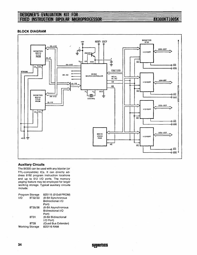
Auxiliary Circuits The 8X300 can be used with any bipolar (or TTL·compatible) ICs. It can directly address 8192 program instruction locations and up to 512 1/0 ports. The memory paging feature may be employed for larger working storage. Typical auxiliary circuits include:
Program Storage 110 8T32/33
8T35/36
8T31
8T39 Working Storage
34
82S115 (512x8 PROM) (8-Bit Synchronous Bidirectional 1/0 Port) (8-Bit Asynchronous Bidirectional 1/0 Port) (8-Bit Bidirectional 1/0 Port) (Quad Bus Extender) 82S116 RAM
~
C) C)
2~~ _to
VR VCR T ~ IVBO-IVB7
8)1(300 MICROCONTROLlER MCLK,
SC,WC -LB
FiB I----
X'4FJlj GNl S.OOMHz
A
825116 ~
256)1(8 RAM
I-=-ME
9i!1DOliC9
r---Me
...
~ ME
....
f--:=-ME
h
'-----ME
SIGNETICS 8T32
flO PORT
I I
Ii'OPORT
I I
1/0 PORT
I I
/10 PORT
I I
UDO-UD1
'""
UDO·UD7
UDO-UD7
UDO-UD7
... > ~
-.... -
>
...., ....,
>
.... ..., .... ...,
-'" ">
...., ~ -
BIC
BOC
BIC
BOC
DESCRIPTION The 8X300 Programming Course is an audio/visual course designed to assist system logic designers with little or no previous microprocessor programming experience to confidently and effectively design and generate software for his own application.
The8X300 Programming Course consists of a series of 13 modular lessons. Each lesson consists of an audio tape and interactive course materials. Two short lessons describe 8X300 hardware features, internal architecture, systems configuration and interfaces, support devices and introduce a variety of software and prototype development tools. The user is then introduced to software and program organization concepts and terminology followed by detailed specification and analysis of instruction formats and operations in six short modules. Opportunity is provided to those students with basic programming skills to bypass one or more of these lessons. A separate lesson on program management and recordkeeping requirements is a natural bridge between instruction details and multi-instruction sequences. The remaining four modules of the course describe a variety of applications processes and specific techniques for effective program design and management. Particular emphasis is given to practical approach and choice of optional solutions. Throughout the course, student learning is reinforced and measured through integrated examples and exercises.
FEATURES • Audio/visual • Self-paced course
COURSE CONTENTS 10 Audio tapes in flat-pack album 6 Envelopes containing course notes 1 Folder containing data sheets and appli-
cation notes 1 Tablet of 8X300 programming forms
During the course of training, the audio cassette tapes are used in conjunction with the course notes to provide the audiolvisual aid. Exercises and pretests are also included at the end of each lesson to assist the student in understanding the course material and at the same time set a guideline for self-pacing.
CONTENTS DESCRIPTION
8X300 PROGRAMMING COURSE OVERVIEW
8X300 Hardware Lesson 1 Features and architecture Lesson 2 Support devices and prototype
development tools
8X300 Software Basics Lesson 3 Introduction to software Lesson 4 Instruction formats Lesson 5 Instruction operands
8X300 Instruction Commands Lesson 6 Data movement Lesson 7 Arithmetic logic Lesson 8 Program control Lesson 9 Record-keeping
Multi-Instruction Applications Lesson 10 Part 1 Lesson 11 Part 2
Subroutine Calls And Returns Lesson 12 Part 1 Lesson 13 Part 2
COURSE ABSTRACT Lesson 1-8X300 Features and architecture A brief description of 8X300 features and capabilities is followed by details of architecture and data flow through the 8X300. All pinouts are defined, and timing considerations relative to a minimum 8X300 system configuration are then illustrated and explained.
S(gnOliCS
1. DeSign objectives. 2. 8X300 applications and usage. 3. Capabilities and limitations. 4. Power requirement and support circuit. 5. External timing requirements. 6. Data flow and throughput; processing time. 7. 8X300 architecture. 8. Instruction cycle phases and timing. 9. Details of the Interface Vector and I/O control. 10.lnternal register definition and usage. 11.8X300 minimum system configuration.
Audio Tape: Approximately 33 minutes Student Completion: Approximately 1 hour, 20 min-
utes
Lesson 2- Support Hardware and Prototype development tools Each generic type of IC compatible for use in an 8X300 system configuration is described, using a short form reference to useful devices as an index. Special attention is provided to efficient configuration of working storage and considerations involved in structuring the Interface Vector.
The lesson is concluded with a precise introduction to software support programs and prototype development hardware available to the 8X300 applications designer.
To develop an understanding of support hardware and prototype development tools available for use by the 8X300 system designer.
1. Composite of most useful 8X300-compatible ICs.
2. Explanation: 825215 bipolar ROM 825115 bipolar PROM 825116 bipolar RAM 8T32/33 IV Byte
3. 256-byte working storage configuration.
35
4. Expandable IV byte Interface Vector. 5. Introduction to:
Microcontroller Simulator (MCSIM) Microcontroller Cross Assembler Program (MCCAP) Designer's Evaluation Board Kit 8T32 Address Programmer
Audio Tape: Approximately 20 minutes Student Completion: Approximately 1 hour
Lesson 3-lntroduction to Software This lesson is designed for the programmer who has not previously been exposed to microprocessor software and its relationship to both internal and external hardware associated with the 8X300. An analogy is drawn between software and its relationsh ip to a computer and sheet music as it relates to an orchestra. Technical terms and buzz words related to microprocessors are then introduced and defined.
1. Hardware/software relationships compared with an analogy to a symphonic production.
2. Software technical definitions, symbols, no-menclature.
Audio Tape: Approximately 15 minutes Student Completion: Approximately 30 minutes
Lesson 4-8X300 Instruction/Data Formats This lesson provides basic information on 8X300 instruction and data formats. I nstruction classes, including opcode definition and operand introduction, are related to fixed instruction formattypes. A brief review of number systems, particularly as they relate to the 8X300, is optionally stud ied by the user.
Outline: 1. General and specific instruction formats. 2. Instruction formats (5) definition. 3. Definition of instruction commands; relation
ship to formats. 4. Operand introduction-effect on format desig
nation. 5. Data format description. 6. Review of number systems; emphasis on binary
and octal (option).
Audio Tape: Approximately 15 minutes Student Completion: Approximately 30 minutes
Lesson 5-8X300 Instruction Operands The 8X300 instruction set is powerfully enhanced by its unique operand configuration. In this lesson, stress is placed on definition and flexibility of all operands as they are written within each instruction class. Using the architecture block diagram, the relationship of each operand to the control of specific internal 8X300 circuits is stressed. Review of all instruction formats is provided, thus laying the groundwork for detailed discussion of the instruction classes themselves.
36
Outline: 1. Description of all operands (S, D, R/L, I, A) in
detail. 2. Software definition of all registers; their fea
tures and constraints. 3. Specification of operand control on related
hardware. 4. Summary of formaVoperand relationship.
Audio Tape: Approximately 20 minutes Student Completion: Approximately 35 minutes
Lesson 6-8X300 Data Movement Commands The flexibility of data movement and manipulation are keys to a solid understanding of the 8X300. Within this framework, data movement instructions MOVE and TRANSMIT are exposed. Stress is laid on execution of these instructions with respect to manipulation of data by operand controlled logic distributed within the 8X300 internal data path. Emphasis is placed on dynamic movement of data when registers or selected 1/0 are designated in any combination as source or destination. Applications and possible software characterization of external hardware are introduced.
Outline: 1. MOVE: Registerto Register: Registerto I/O; I/O
to R~gister; I/O to I/O. Emphasis on IVL/IVR I/O Port Addressing.
2. TRANSMIT: Immediate Register Load; fixed data to selected I/O. Flexibility and constraints.
3. Summary table of data movement internal con-trols.
Audio Tape: Approximately 25 minutes Student Completion: Approximately 45 minutes
Lesson 7-8X300 Arithmetic/Logic Commands With prior emphasis on with reference to data movement and manipulation as a base, ALU functions and their resultant effect on data are stressed. Introduction to applications arising from implementation of ALU instructions, and resultant minimization of external hardware required in nonmicroprocessor systems, is provided. Instruction is provided at the machine language level in order to establish a firm foundation for multi-instruction applications later in the course.
Outline: 1. Arithmetic ADD instruction; function of R-10. 2. LOGICAL AND instruction. 3. EXCLUSIVE OR instruction. 4. Review of ALU and data movement commands
through self-administered exercises.
Audio Tape: Approximately 15 minutes Student Completion: Approximately 30 to 50 min
utes, based on completion of optional review exercises.
lii!lDOliC9
Lesson 8-8X300 Program Control Commands A statement of the purpose of program control instructions is followed by a detailed, analysis of each at machine language level. Software partitioning of control storage memory into pages and segments is explained. Emphasis is placed on the dynamics of linking fixed and processed bit patterns into working control storage access addresses. The relationship between absolute memory addresses and immediate operand fields contained within program control instructions is stressed through explanation of, and interactivity with, simplified conversion tables.
Outline: 1. Relationship to 8X300 internal architecture and
instruction cycle timing. 2. Memory mapping; software implementation in
program control paging, segments, relative displacement.
3. Boundary limits as function of register and selected I/O designation.
4. Solutions for maximizing program control flexibility.
5. Program control examples: XEC, NZT, and JMP.
6. Practical implementation in working program. 7. Description/usage of address/immediate oper-
and translation tables.
Audio Tape: Approximately 35 minutes Student Completion: Approximately 1 hour, 10 min-
utes
Lesson 9-Record Keeping Considerations This lesson demonstrates the need for effective record keeping as a necessary parallel to multi-instruction software requirements. Top-Down programming concepts are defined. Symbolic labeling of address and data fields are described by purpose and usage. Techniques which must be considered by the programmer in analyzing the need for, and subsequent preparation of, housekeeping routines are proposed. A variety of programming forms, tailored for use by 8X300 software writers, are introduced and explained.
Outline: 1. Need for program enhancement through effec
tive record keeping. 2. Top-Down program design concept introduc
tion. 3. Programmer record maintenance tools and ap
plication. 4. CPU record maintenance tools and applica
tions. 5. Record keeping for I/O, process, and address
control. 6. Symbolic labeling, usage. 7. Effect of poor record keeping applications on
CPU program execution. 8. Techniques for effective record keeping. 9. Programming forms introduction and descrip
tion.
Lesson 10-Multi-lnstruction Applications The first of two applications lessons describes software sequences for subtracting, inclusive OR, mask variations, basic interrupt processes, CPU and I/O initiated delays, and data deserialization. A number of alternative approaches and solutions to each problem are developed. Transition from single to multiple instruction sequences increases in complexity as the lesson progresses. Housekeeping functions integral to the implementation of each topic are stressed.
Outline: 1. 1's complement, 2's complement, and subtrac
tion. 2. Negative numberlimmediate operand conver-
sion tables. 3. Software implemented counters, applications. 4. Time delay concepts and applications. 5. Data masking implementation and usage. 6. Masked interrupt process techniques, I/O in-
terrupt handling. 7. INCLUSIVE-OR software and applications. 8. Multiple byte addition and storage features. 9. Serialization and deserialization of data.
• applications • overall program considerations • software options • significant bit handling • interlock with slower 1/0
10.Timing and clock generation. 11.Clocked serializing techniques. 12.CPU and 1/0 controlled delay options includ-
ing fine tuning techniques. 13.Fixed I/O controlled data serialization.
Audio Tape: Approximately 37 minutes Student Completion: Approximately 1 hour 30 min-
utes
Lesson 11-Multi-lntroduction Applications The second of two applications lessons focuses on multi-bit pattern detection and generation. Applications for data serialization at variably rates determined by 110, and service routines based on complex liD status, are described. The subject of interrupt handling is reopened, this time to provide techniques for processing multi-level prioritized interrupts typically found in complex externally controlled I/O systems. Tradeoffs between speed of handling interrupts and conservation of control storage are described, then implemented. Techniques learned in previous examples are then chos-
en to implement a typical controls application monitoring and service scheme.
Outline: 1. Pattern generation and detection. 2. Cost effective sequence options. 3. XEC instruction flexibility. 4. Multi-line 1/0 status discrimination techniques. 5. Multiple use of working register; application. 6. Flexible routine exit options. 7. Alternatives:
Control storage conservation. Expectedlunexpected scheduled 1/0 status handling.
8. Multi-level statuslinterrupt priorities. 9. Software designed for rapid interrupt detec
tion. 10.Complex system's interrupt handling and prior-
itizing.
Audio Tape: Approximately 35 minutes Student Completion: Approximately 1 hour, 20 min
utes
Lesson 12-Subroutine Calls & Returns-1 Subroutine calls and returns are examined from 2 basic points of view. These are:
1. Program organization and management. 2. The mechanics of creating effective routines
and process sequences.
After a review of program control commands presented in previous lessons, this lesson presents the theory of Single and multi-level routine access with sequentially increased complexity. Possible programmer errors are defined and practical solutions for their prevention are suggested. Tradeoffs in memory conservation, speed, and dynamic operations related to program organization and execution are examined. 8X300 program control instruction flexibility is stressed.
Outline: 1. Introduction: The need for effective overall
program organization and management. 2. Review of elementary intra-routine access
procedures. 3. 8X300-oriented return address link:
Basic use of working register. Return link saved in working storage; release of
register. Return jump table usage; Memory mapping. 4. Routine nesting; concept, need, principles,
considerations. 5. Practical two-level routine access and return. 6. Simplified multi-level subroutinelreturn struc
ture.
lii!lDotiCS
7. Legal and illadvised sequences; constraints; options to eliminate error.
8. Page and segment boundary management. 9. Diagrammed analysis of nesting multi-level
program structures. 10.Practical choice of all/return instruction proce-
dures based on program segment definition: Terminal Inline Bypass Multiple access
11.Summary of fundamental program structuring principles.
Audio Tape: Approximately 37 minutes Student
Completion: Approximately 1 hour, 10 min-utes
Lesson 13-Subroutine calls and Returns-2 Implementation of subroutine multi-level access control through software configuration of the RETURN ADDRESS STACK (RAS) is presented. Different types of RAS are defined with detailed exposition of one easily adapted to 8X300 usage. Configuration of the RAS in working storage and accompanying universal jump table access is presented. The use of intermediate software processes for dynamic access of, and return from, nested program segments is described. Simplification of program complexity is stressed.
Program management considerations are introduced, including subtleties involved in program packing for control storage conservation and error correction involving page and segment boundary management.
Outline: 1. RETURN ADDRESS STACK definition and
architecture. 2. Software generation of RAS:
Usage of working storage Universal Jump Table
3. Direct versus indirect subroutine access/return.
4. Implementation of indirect processes details, constraints, options.
5. Relocatable addressing in multi-level sequencing.
6. Program packing; advantages and need. 7. Page and segment boundary management er-
rors and solutions.
Audio Tape: Approximately 35 minutes Student Completion: Approximately 1 hour, 10 min
utes
37
DESCRIPTION The 8X300 Assembler is a program which accepts source code written in the 8X300 assembly language and which produces both a listing of the symbolic program and an object module in one of three formats: MCSIM, ROM Simulator or BPNF.
The assembler is written in ANSI standard Fortran and is approximately 2800 card images in length. It requires some rewindable 110 medium such as disk or tape for temporary storage, an input device to read source code and two output devices, one to output the assembler listing and one to output the object module. If desired, the assembler may be compiled and linked to execute in overlays.
The assembler consists of two passes which build a symbol table, issue helpful error messages, produce an easily readable pro .. gram listing and output a computer readable object module.
FEATURES • Macros nested to three levels • Conditional assembly • Address arithmetic • Automatic procedure/subroutine han ..
dllng • Reserved symbols for registers • Multiple entry to procedures • Symbolic machine operation codes • Symbolic address assignment references • Symbolic data creation statements (IV
Byte References) • Free format source code • Syntax error checking • Self-defining constants • Assembly listing control statements • ASCII character code • Comment statements and comment
areas • Forward referencing
38
MCCAPLANGUAGE The assembler recognizes three types of statements: comment statements, machine instructions, and pseudo .. ops (directives>.
Comment statements are used to document a listing. They must contain an asterisk in column 1 and may contain any legal character in the other 79 columns.
Machine instruction statements are those statements that generate instruction(s) to be executed by the 8X300 processor. Machine instruction statements include:
MOVE
ADD
AND
XOR
XEC
XMIT
NZT
JMP CALL
RTN
SEL
Move byte from one location to another. Add the byte in one location to the byte in the auxiliary register and store the result in another tocation. AND the byte in one location with the byte in the auxiliary register and store the result in another location. Exclusive OR the byte in one location with the byte in the auxiliary register and store the result in another location. Execute the instruction at the specified address. Transmit the literal (immediate data) contained in this instruction to the specified location. Jump to the specified address if the value in the specified location is not zero. Jump to the specified address. Transfer control to a procedure or an entry point. Returns control from a procedure or an entry point. Places the address of an IV Byte variable into the IVL or the IVR register.
Pseudo·Ops (or Directives) are commands to the assembler, but have no meaning to the 8X300 processor.
lil!lDOliCIi
EOU
SET
L1V
RIV
'PROG
PROC
ENTRY
END
ORG
OBJ
IF
ENDIF
LIST
NllST
EJCT SPAC MACRO
Assigns a value to the symbol in the label field. Identical to EQU, except that the symbol may be redefined by another SET statement. ASSigns a symbolic name to the address, position and pre· cision of the "left bank" Interface Vector Byte variable. Identical to L1V, except that the aSSignment is made to the "right bank" 110 Field. Introduces and names the main program. Introduces and names a procedure. Specifies an additional entry point to a procedure. Terminates a procedure, a program or a MACRO. Changes the value of the location counter. Specifies the format of the object module. Introduces source statements subject to conditional assembly. Terminates the source statements subject to conditional assembly. Specifies the list and punch options. Negates the list and punch options. Advances listing to next page. Advances listing to next line. Defines the source statements generated a macro call.
AVAILABILITY The assembler is available on NCSS, GE and TYMSHARE timesharing services. It is also available from Signetics on 9-track magnetic tape written in EBCDIC in 80-character unblocked records at a density of 800 bpi.
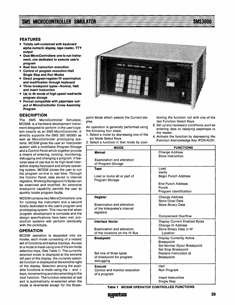
FEATURES • Totally self-contained with keyboard
alpha-numeric display, tape reader, TTY output
• Dual MlcroControliers: one to run Instntment, one dedicated to execute user', program
• Real time instruction execution • Control of program execution-Halt
Single Step and Run Modes • Direct program/register/IV examination
and modification through keyboard • Three breakpoint types-Normal, Halt
and Insert Instruction • Up to 4k words of high speed read/write
program storage • Format compatible with papertape out
put of MicroControlier Cross Assembly Program
DESCRIPTION The SMS MicroController Simulator, MCSIM, is a hardware development instrument designed to perform in the user's system exactly as an SMS MicroController. It directly supports the SMS 300 (8X30Q) as well as MicroController prototyping systems. MCSIM gives the user an Interpreter system with a modifiable Program Storage and a Control Panel which together provide a means of entering, running, monitoring, debugging and changing a program. It features ease of use due to its high level interactive display/keyboard and simple operating system. MCSIM allows the user to run his program on-line in real time. Through the Control Panel, data stored in internal registers, Working Storage and IV Bytes can be examined and modified. An extensive breakpoint capability permits the user to quickly locate program faults.
MCSIM contains two MicroControliers: one for running the instrument and a second totally dedicated to the user's program and prototyping system. This insures that when program development is complete and the design specifications have been met, production systems will perform identically with the prototype.
OPERATION MCSIM operation is separated into six modes, each mode conSisting of a related set of functions and status displays. Access to a mode is made using one ofthe six mode selection keys. (See Table 1), The currently selected mode is displayed at the extreme left part of the display; the currently selected function is displayed at the extreme right of the display. Selection among the available functions is made using the t and t keys, incrementing and decrementing tothe next function. The function selected at last exit is automatically re-selected when the mode is re-entered except for the Break-
pOint Mode which selects the Current display.
An operation is generally performed using the following four steps: 1. Select a mode by depressing one of the
six Mode Select Keys. 2. Select a function in that mode by post-
MODE
Manual
Examination and alteration of Program Storage
Tape
Load or dump all or part of Program Storage
Register
Examination and alteration of the Interpreter's internal registers
Interface Vector I
Examination and alteration of the locations on the IV Bus
Breakpoint
Set one of three types of breakpoint for program debugging
Execute Control and monitor execution of a program
tioning the function roll with one of the two Function Select Keys.
3. Set up any necessary conditions, such as entering data or readying papertape in the reader. '
4. Activate the function by depressing the Function Acknowledge Key (FCN/ ACK)'
FUNCTIONS
Change Address Store Instruction
Load Verify Begin Punch Address
End Punch Address Punch Program Identification
Change Address Store Octal Data Store Binary Data
Complement Overflow
Display Current Enabled Bytes Change IV Address Store Binary Data in IV
Location
Display Currently Active Breakpoint Set Normal (Sync) Breakpoint Set Stop Breakpoint Replace Instruction at Breakpoint
Halt Run Program
Insert Instruction Single Step
Table 1 MCSIM OPERATOR CONTROLLED FUNCTIONS
Ii!lDDliCI 39
SPECIFICATIONS Control Panel The Mode Select Keys and the Function Select Keys used in combination give the user 26 possible functions to accomplish complete loading and testing of the program. Eac~ Mode Select Key accesses a set of functions, one of which is chosen using the Function Select Keys.
Status Messages Message displays are used to indicate special conditions which may result from the operation of MCSIM:
Data Input/Output
COMPONENTS
POWER ON, MCSIM SYSTEM START ???MORE THAN ONE KEY PRESSED UNABLE TO READ TAPE. RESTART UNDEFINED MEMORY ADDRESS (octal address) INVALID INSTRUCTION (instruction code) LOADING INTERRUPTED, RESTART V'FYING INTERRUPTED, RESTART P'CHING INTERRUPTED, RESTART NO VERIFY (octal address, tape data, memory data) CLEAR RESET LINE TO START RUNNING CLEAR HALT LINE TO START RUNNING INVALID 8-BIT OCTAL VALUE (octal value) UNDEFINED IV BYTE ADDRESS (octal address)
DESCRIPTION
Panel 36 character self scan display for messages and data readout 12 key numeric keyboard for data entry/modification
Tape Reader 120 character/second tape reader for high speed data entry (ASCII format)
TTY 20mA current loop output for listing of program code on Teletype® terminal
PHYSICAL CHARACTERISTICS Power 115V or 230V ± 10%
50 or 60Hz ± 10% 350 watts/min. to 750 watts/max. (Power dissipation dependent on the number of Simulation Modules configured in the system)
Dimensions 7 inches high x 17 inches wide x 19 inches deep
Installation May be used on table or may be installed in standard 19 inch rack with mount adapters
Weight 65 Ibs. net, 75 Ibs. shipping
Ventilation Air Flow 120 CFM
Environmental 0° to 55°C,Relative Humidity to 90%.
40 SmOOliC!i
Sync Output Output pulse whenever address breakpoint is reached.
System Interface MCSIM is connected to the user's prototyping system via a single ribbon cable. This cable terminates in either a MicroController Simulation Module or a dual in-line plug which is pin for pin compatible with the SMS 300 Interpreter. There are two different simulation modules to exactly match presently available MicroController systems. Selection of the proper input/output connector makes a MCSI M appear to be physically and electrically equivalent to a production MicroController or Interpreter.
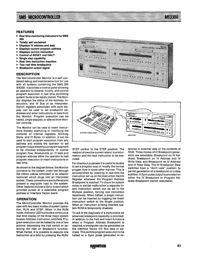
FEATURES • Real time monitoring instrument for SMS
300 • Totally self contained • Displays IV address and data • Displays current program address • Displays current instruction • Control of RESET and HALT • Single step capability • Real time instruction insertion • Two real time breakpoints • Breakpoint output signal
DESCRIPTION The MicroControlier Monitor is a self contained debug and maintenance tool for use with all systems containing the SMS 300 (8X300)' It provides a control panel allowing an operator to observe, modify, and control program execution in real time permitting system faults to be rapidly traced. The Monitor displays the status of the Address, Instruction, and IV Bus of an Interpreter. Switch registers associated with each display can be used to set breakpoint addresses and enter instructions or data from the Monitor. Program execution can be halted, single stepped, or altered from Monitor controls.
The Monitor can be used to insert instructions thereby examining or modifying the contents of internal registers, Working Store, and IV Bytes. In addition, it can be used to start program execution from any address and enable the operator to set program loops allowing a program segment to be checked independently of normal program flow. Breakpoints on IV data and program address allow the operator to halt program execution or insert instructions in real time.
As shown in the diagram below, the Monitor connects to the system under test through flat ribbon cables (provided) or an adaptor (optional) which plugs into an Interpreter socket. These connections are buffered and present a negligible load to the system. Other features include a Sync output which provides pulses at a selectable program address or Interface Vector event.
OPERATION The MicroControlier Monitor provides the user with two basic modes of system operation, RUN and STEP. When in the RUN mode, indicator LED's provide a continuous real time display of the three major system busses: Address, I nstruction, and Data. Program execution can be halted by one of two actions: depressing the Halt switch or selecting the Halt on Breakpoint function. When halted, it is possible to execute one instruction at a time by pressing the RUN/
STEP control to the STEP position. The readout shows the current (static) bus information and the next instruction to be executed.
For checkout purposes it is useful to be able to set a program loop or modify the normal progam flow in some other manner. This is accomplished by inserting in real time the instruction set up on the Instruction Switch Register whenever the Program Address Breakpoint is reached. To check for system noise or similar malfunction a separate Insert Instruction switch can be set to the Multiple position, forcing one instruction repetitively. When halted, a single instruction can be inserted by toggling the Insert Instruction switch to the Single position. When an instruction is being inserted, system ROM is temporarily disabled.
To aid in the diagnosis of a malfunction an advanced breakpoint capability is provided. In addition to the Halt and Insert functions when a Program Address Breakpoint is reached, a breakpoint can be generated on the Interface Vector (IV) Bus data or address. This permits program execution to be halted or a Sync pulse generated in re-
lil!llOliCS
MSIIOO
sponse to external data or the contents of RAM. Three modes of IV Breakpoint generation are selectable: Breakpoint on IV Address; Breakpoint on IV Address and IV Write Data; and Breakpoint on IV Address and IV Read Data. The IV Breakpoint Data switches have a "don't care" position to permit generation of a breakpoint on a data subfield. A Sync pulse output is provided on either the IV Breakpoint or Program Address Breakpoint (switch selectable).
41
SPECIFICATIONS
Controls
RUN/STEP
INSERT INST
RESET/HALT
PGM ADR BKPT
IV BKPT
BKPT UPON
SYNC SOURCE
Switch Registers
INSTRUCTION
BREAKPOINT ADDRESS
IV BREAKPOINT ADDRESS
BANK
IV BREAKPOINT DATA
Displays
RUN
CURRENT INSTRUCTION
CURRENT PROGRAM ADDRESS
IN XEC RANGE
BANK
CURRENT IV ADDRESS CURRENT IV DATA Outputs
SYNC PGM EN(U
Cycle Time
Function
Sets operation mode, continuous execution (RUN) or single step (STEP). Unconditionally causes execution of the instruction in the Instruction Switch Register. Three position switch used to unconditionally HALT program execution or RESET Interpreter's Program Counter to zero. Selects appropriate function to be performed when Program Address Breakpoint is reached: HALT-halt on breakpoint, INSERTreplace normal instruction with instruction set into Instruction Switch Register. OFF-program execution unchanged by breakpoint. Selects appropriate function to be performed when IV Breakpoint is reached: HALT-halt on breakpoint, OFF-program execution unchanged by breakpoint. Selects IV Breakpoint on one of three conditions: specified IV address, specified write data at IV address, specified read data at the IV address. Selects source for output Sync pulse, IV Breakpoint or Program Address Breakpoint. Sync pulse always available at breakpoint regardless of function selected by breakpoint controls.
Sixteen two position switches for entering instruction to be inserted (during breakpoint or insert instruction controll.
Thirteen two position switches to select program breakpoint address.
Eight two position switches to select IV byte breakpoint address or Working Store breakpoint address ..
Selects display of LB (Left Bank) or RB (Right Bank) IV address information. Also selects either LB or RB for IV breakpoint.
Eight three position switches, 0, 1, X (don't care), to select IV Data Breakpoint.
LED display indicating when Interpreter not halted.
LED display of the binary value of next instruction to be executed.
LED display of the binary address of the next instruction to be performed.
LED display indicating that the value of the Interpreter's program counter and address register may not match because the previous instruction command was "Execute."
Displays band addressed by the current instruction (left bank or right bank). Shows the binary address of the currently enabled IV Byte or Working Store location. Binary display of the data on the IV bus.
Pulse output whenever the switch selected breakpoint occurs. A low true signal used to enable or disable system program ROM (required only when Interpreter adaptor is used).
The Monitor can be adjusted to work with any MicroControllerbased system with a cycle time of 200ns to 2JJ.s.
42 I!DOliCI
PHYSICAL CHARACTERISTICS
Power 115Vac ± 10% at 0.75 amp max. 230Vac ± 10% at 0.38 amp max. (optionall 47-63Hz
Dimensions 7" H x 17.5" W x 3" 0
Installation May be used on table or may be installed in standard 19 inch rack (using optional adap-tors).
Weight 10 Ibs. shipping
net, 13 Ibs.
Ventilation Forced air, 120 CFM. Environmental 0° to+ 50°C, relative hu-
m idity to 90% Cables 2 provided, 3 feet long

APPIIOATlon IIIIIOS
S!!IDl!liCS 43

44 Ii!!)DOliC!i
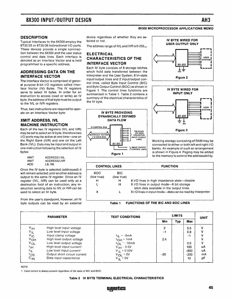
8X300 INPUT/OUTPUT DESIGN AH3
DESCRIPTION Typical interfaces to the 8X300 employ the 8T32/33 or 8T35/36 bidirectional 1/0 ports. These devices provide a single connnection between the 8X300 and the user status control and data lines. Each interface is denoted as an Interface Vector and is field programmed to a specific address.
ADDRESSING DATA ON THE INTERFACE VECTOR The Interface Vector is comprised of general purpose 8-bit 1/0 registers called Interface Vector (IV) Bytes. The IV registers serve to select IV bytes. In order for an instruction to access (read or write) an IV byte, the address of that byte must be output to the IVL or IVR registers.
Thus, two instructions are required to operate on an Interface Vector byte:
XMIT ADDRESS, IVL MACHINE INSTRUCTION Each of the two IV registers (IVL and IVR) may be set to select an IV byte, therefore two 1/0 ports may be active at one time-one on the Right Bank (IVR) and one on the Left Bank (IVL). Data may be input and output in one instruction following the selection of IV bytes:
XMIT ADDRESS1,IVL XM1T ADDRESS2,IVR ADD LB, RB
Once the IV byte is selected (addressed) it will remain selected until another address is output to the same IV register. Since an IV register (IVL, IVR) can be used only as a destination field of an instruction, any instruction sending data to IVL or IVR can be used to select an IV byte.
From the user's standpoint, however, all IV byte outputs can be read by an external
PARAMETER
V IH High level input voltage V IL Low level input voltage VIC Input clamp voltage VOH High level output voltage VOL Low level output voltage ItH High level input current1 I,L Low level input current1 lOS Output short circuit current C IN Data input capacitance
NOTE
8X300 MICROPROCESSOR APPLICATIONS MEMO
device regardless of whether they are selected or not.
The address range of IVLand IVR is 0-25510,
ELECTRICAL CHARACTERISTICS OF THE INTERFACE VECTOR Each IV byte consists of 8 storage latches which hold data transferred between the Interpreter and the User System, 8 tri-state input/output lines and 2 input/output control lines, called Byte Input Control (BIC) and Byte Output Control (BOC) as shown in Figure 1. The control lines functions are summarized in Table 1. Table 2 contains a summary of the electrical characteristics of the IV byte.
IV BYTE PROVIDING DYNAMICALLY DEFINED
DATA FLOW
IV CONTROL BUS
IV BYTE WIRED FOR USER OUTPUT ONLY
+5V":"
Figure 2
IV BYTE WIRED FOR INPUT ONLY
Figure 3
r--, I I I I
USER I SYSTEM.
I I L ___ 01
Working storage consisting of RAM may be connected to either or both left and right 1/0
'--___ )~~NUTT:g~[I~~~ banks. An example of such an arrangement
Figure 1 is shown in Figure 4. Paging may be added to the memory to extend the addressability.
CONTROL LINES FUNCTION
BOC (low true)
H L
x
BIC (low true)
H H
8 1/0 lines in high impedance state-disable 8 110 lines in output mode-8 bit storage
latch data available in the output lines. L 8110 lines in input mode-data can be read by Interpreter
Table 1 FUNCTIONS OF THE BIC AND BOC LINES
TEST CONDITIONS LIMITS UNIT
Min Typ Max
2 5.5 V -1 0.8 V
IIL:= -5mA -1 V 10H:= 1mA 2.4 V I OL := -16mA 0.5 ·V V IH .:: 5.5V 100 uA V IL = 0.50V -800 uA VOL = OV -20 -200 mA
V IL = OV 12 pF
1. Input current is always present regardless of the state of BIC and BOC.
Table 2 IV BYTE TERMINAL ELECTRICAL CHARACTERISTICS
S(gOOliC!i 45
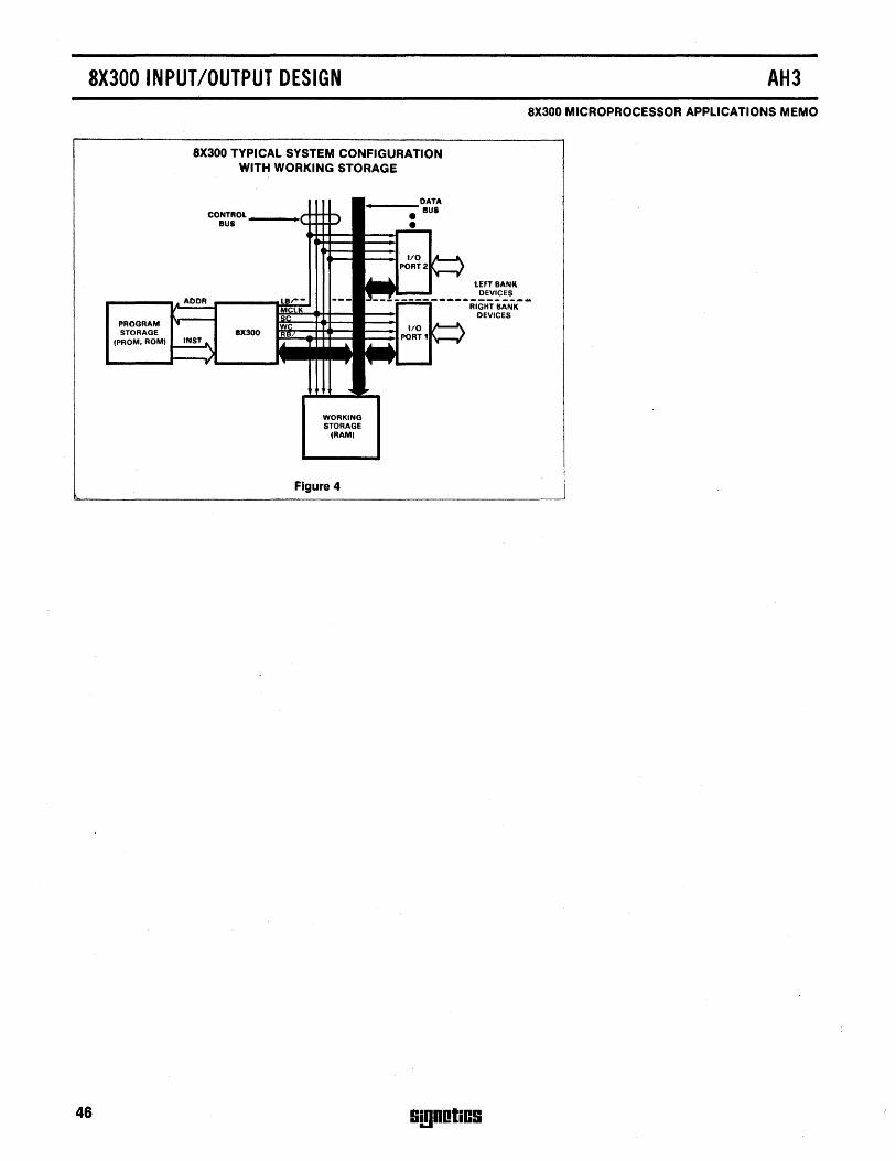
8X300 INPUT/OUTPUT DESIGN
46
PROGRAM STORAGE
8X300 TYPICAL SYSTEM CONFIGURATION WITH WORKING STORAGE
ADDR
8X300 IPROM. ROMI .---__ ".
WORKING STORAGE
CRAMI
Figure 4
Si!lDDliC!i
AH3 8X300 MICROPROCESSOR APPLICATIONS MEMO
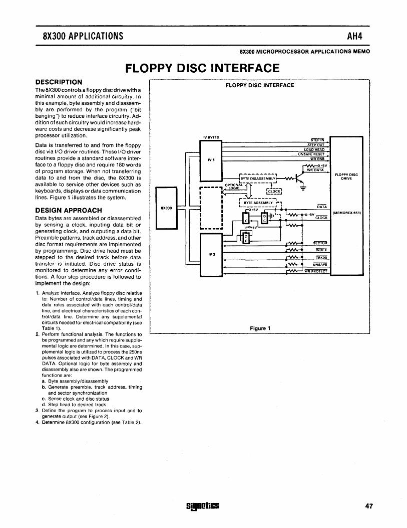
8X300 APPLICATIONS AH4 8X300 MICROPROCESSOR APPLICATIONS MEMO
FLOPPY DISC INTERFACE DESCRIPTION The 8X300 controls a floppy disc drive with a minimal amount of additional circuitry. In this example, byte assembly and disassembly are performed by the program ("bit banging") to reduce interface circuitry. Ad· dition of such circuitry would increase hardware costs and decrease significantly peak processor utilization.
Data is transferred to and from the floppy disc via I/O driver routines. These I/O driver routines provide a standard software interface to a floppy disc and require 180 words of program storage. When not transferring data to and from the disc, the 8X300 is available to service other devices such as keyboards, displays or data communication lines. Figure 1 illustrates the system.
DESIGN APPROACH Data bytes are assembled or disassembled by sensing a clock, inputing data bit or generating clock, and outputing a data bit. Preamble patterns, track address, and other disc format requirements are implemented by programming. Disc drive head must be stepped to the desired track before data transfer is initiated. Disc drive status is monitored to determine any error conditions. A four step procedure is followed to implement the design:
1. Analyze interface. Analyze floppy disc relative to: Number of control/data lines, timing and data rates associated with each control/data line, and electrical characteristics of each control/data line. Determine any supplemental circuits needed for electrical compatibility (see Table 1).
2. Perform functional analysis. The functions to be programmed and any which require supplemental logic are determined. In this case, sup~ plemental logic is utilized to process the 250ns pulses associated with DATA, CLOCK and WR DATA. Optional logic for byte assembly and disassembly also are shown. The programmed functions are: a. Byte assembly/disassembly b. Generate preamble, track address. timing
and sector synchronization C. Sense clock and disc status d. Step head to desired track
3. Define the program to process input and to generate output (see Figure 2).
4. Determine 8X300 configuration (see Table 2).
IIX300
FLOPPY DISC INTERFACE
IV IIYTES
IV'
,--------, 8YTE DISASSEM8LY-JVV\r~
OPTIONki- -----1-J ,..----, LOGIC: r.:~--;"I
~~O~!J I I I I I I
I I '-----. Iv2
S!lDOliCS
....- -------, I 8YTE ASSEM8L Y .. , '-_________ .J , DATA
+!5V .--+--4 ....... -----=:.:...:..:..:..~ IJVV\.--e-.<l +!5V __
CLOCK
WR PROTECT
Figure 1
FLOPPY DISC DAIVE
/MEMOAEX 6511
47
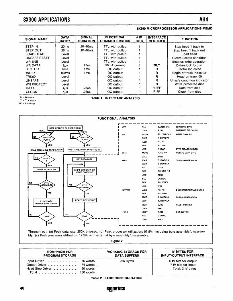
8X300 APPLICATIONS
SIGNAL NAME
STEP IN STEP OUT LOAD HEAD UNSAFE RESET WR ENB WR DATA SECTOR INDEX TRKOO UNSAFE WR PROTECT DATA CLOCK
R = Resistor T = Transistor
FF = Flip-Flop
DATA RATE-1
20ms 20ms Level Level Level 2f.1s 5ms
160ms Level Level Level 4f.1s 4f.1s
AH4 8X300 MICROPROCESSOR APPLICATIONS MEMO
SIGNAL ELECTRICAL #IV INTERFACE FUNCTION DURATION CHARACTERISTICS BITS REQUIRED
.01-10ms TTL with pullup 1 Step head 1 track in
.01-10ms TTL with pullup 1 Step head 1 track out TTL with pullup 1 Load head TTL with pullup 1 Clears unsafe condition TTL with pullup 1 Enables write operation
. 25f.1s SOmA current 1 2R,T Data/clock to disc 1ms DC output 1 R Sector indicated 1ms OC output 1 R Begin of track indicator
OC output 1 R Head on track 00 OC output 1 R Unsafe condition indicator OC output 1 R Write protected disc
. 25f.1s DC output 1 R,2FF Data from disc
. 25f.1s DC output 1 R,FF Clock from disc
Table 1 INTERFACE ANALYSIS
FUNCTIONAL ANALYSIS
.----------------------I WR1 XEC DATBLE (R3) GET DATA BYTE
I XMIT B. R1 INITIALIZE BIT COUNT
I WR2
I I I I I
MOVE
XMIT
ADD
NZT
JMP
R2.DWRDAT WRITE DATA BIT
1.DWRDAT
R1. R1
R1. WR3
BYTE DISASSEMBLED
,!::;~==;tr-----'r----.' __________ J WR3 MOVE
NXTWR
R2(1). R2 ROTATE DATA BYTE
48
CALL WAIT
WR4 XMIT O.DWRCLK CLOCK GENERATION
XMIT 1.DWRCLK
SEL DSTAT
NZT DINDEX. '+2
JMP TEND
SEL DCMMD
NO NZT R5. TENDL
JMP WR2
NXTWR ADD R3. R3 DECREMENT DATA POINTER
NZT R3. WRO
XMIT O.DWRCLK CLOCK GENERATION
XMIT 1.DWRCLK
XMIT 2. R3 RESET POINTER
JMP WR1
TEND XMIT 1. R5 SET SWITCH NO SEL DCMMD --------., JMP WR2
I L _____________ ~-------
Through put: (a) Peak data rate: 250K bits/sec. (b) Peak processor utilization: 97.5%, including byte assembly/disassembly. (c) Peak processor utilization: 12.2%, with external byte assembly/disassembly.
Figure 2
ROM/PROM FOR WORKING STORAGE FOR IV BYTES FOR PROGRAM STORAGE DATA BUFFERS INPUT/OUTPUT INTERFACE
Input Driver ..................... 76 words 256 Bytes 6 IV bits for output Output Driver .................... 74 words 7 IV bits for input Head Step Driver ................ 30 words Total: 2 IV bytes
Total .......................... 180 words
Table 2 8X300 CONFIGURATION
Gi!lDOliCG
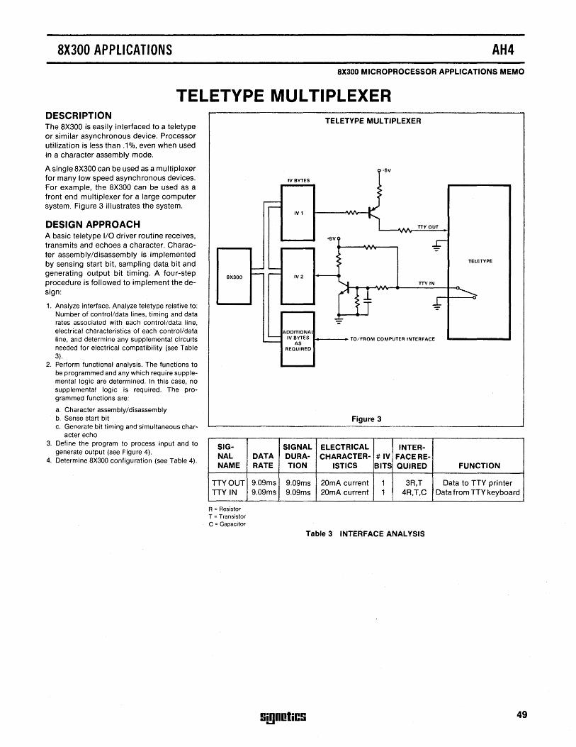
8X300 APPLICATIONS AH4 8X300 MICROPROCESSOR APPLICATIONS MEMO
TELETYPE MULTIPLEXER DESCRIPTION The 8X300 is easily interfaced to a teletype or similar asynchronous device. Processor utilization is less than .1%, even when used in a character assembly mode.
A single 8X300 can be used as a multiplexer for many low speed asynchronous devices. For example, the 8X300 can be used as a front end multiplexer for a large computer system. Figure 3 illustrates the system.
DESIGN APPROACH A basic teletype I/O driver routine receives, transmits and echoes a character. Character assembly/disassembly is implemented by sensing start bit, sampling data bit and generating output bit timing. A four-step procedure is followed to implement the design:
1. Analyze interface. Analyze teletype relative to: Number of control/data lines, timing and data rates associated with each control/data line, electrical characteristics of each control/data line, and determine any supplemental circuits needed for electrical compatibility (see Table 3).
2. Perform functional analysis. The functions to be programmed and any which require supplemental logic are determined. In this case, no supplemental logic is required. The programmed functions are:
a. Character assembly/disassembly b. Sense start bit c. Generate bit timing and simultaneous char
acter echo 3. Define the program to process input and to
generate output (see Figure 4). 4. Determine 8X300 configuration (see Table 4).
8X300
SIG-NAL NAME
TTY OUT TTY IN
R = Resistor T = Transistor C = Capacitor
TELETYPE MULTIPLEXER
I +5V
IV BYTES
:> ~>
r---r---
IV 1
..A TTY OUT .... +5V
* : TELETYPE
- 10......-.>
- r--- IV 2 ~~
TTY IN r 1· ~
-4-~T
"*" ADDITIONAL --- IV BYTES TO/FROM COMPUTER INTERFACE - AS REQUIRED
Figure 3
SIGNAL ELECTRICAL INTER-DATA DURA- CHARACTER- #IV FACERE-RATE TION ISTleS BITS QUIRED FUNCTION
9.09ms 9.09ms 20mA current 1 3R,T Data to TTY printer 9.09ms 9.09ms 20mA current 1 4R,T,C Data from TTY keyboard
Table 3 INTERFACE ANALYSIS
Si!)DotiCS 49
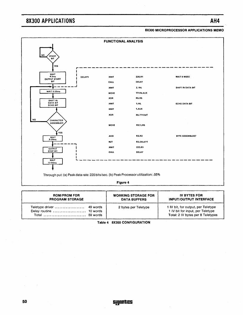
8X300 APPLICATIONS AH4
50
8X300 MICROPROCESSOR APPLICATIONS MEMO
FUNCTIONAL ANALYSIS
r---~-----~~-~-~---~----~~~-------~
NO
I WAIT I 4.Sms
I OUTPUT START BIT I ______ ...J
-------, ----~--~ I
1 , I
DElAY1 XMIT
CALL
XMIT
MOVE
XOR
XMIT
XMIT
XOR
MOvE
ADD
NZT
XMIT
CAll
220.R1 WAIT 9 MSEC
DELAY
2.IVL SHIFT IN DATA BIT
TTYIN.AUX
RS.RS
1.IVL ECHO DATA BIT
1.AUX
RS.TTYOUT
RS(1}.RS
R3.R3 BYTE ASSEMBLED?
R3.DELAY1
220.R1
DELAY
~---------------------------------
Through put: (a) Peak data rate: 220 bits/sec. (b) Peak Processor utilization: .05%
Figure 4
ROM/PROM FOR WORKING STORAGE FOR IV BYTES FOR PROGRAM STORAGE DATA BUFFERS INPUT/OUTPUT INTERFACE
Teletype driver ................... 49 words 2 bytes per Teletype 1 IV bit, for output, per Teletype Delay routine •••.••.••••••......•. 10 words 1 IV bit for input, per Teletype
Total ••...•••••••••••...••••.••• 59 words Total: 2 IV bytes per 8 Teletypes
Table 4 8X300 CONFIGURATION
Si!lDDliCS
8X300 APPLICATIONS AH4 8X300 MICROPROCESSOR APPLICATIONS MEMO
DATA CONCENTRATOR DESCRIPTION The 8X300 multiplexes multiple low speed terminals. It buffers the data in its working storage for efficient transmission over common carrier or other data link facilities. Single inquiry/response terminals are interfaced to a single half-duplex synchronous line via a Universal Asynchronous ReceiveITransmit (UART) interface. This eliminates cabling to each terminal. The 8X300 transfers inquiry and response messages between terminals and a remote computer data base via a data communications line. Various communication data rates are accommodated by simple program modification. Figure 5 illustrates the system.
DESIGN APPROACH The 8X300 polls each terminal requesting an input character or signaling an output character. Each character is transferred over a high speed (9600 baud) synchronous line whose data rate determines the scan time of the 8X300 multiplexing program. The multiplexer program formats polling messages, maintains status, generates and checks the Longitudinal Redundancy Character, performs character recognition, and buffers characters. Additional driver programs are required to communicate with the full duplex data communications line tol from a remote computer data base. A four step procedure is followed to implement the design:
1. Analyze interface. Analyze UART relative to: Number of control/data lines, timing and data rates associated with each control/data line, electrical characteristics of each control/data line and determine any supplemental circuits needed for electrical compatibility (see Table 5).
2. Perform functional analysis. The functions to be programmed and any which require supplemental logic are determined. In this case, no supplemental logic is required. The programmed functions are: a. Maintain current line status b. Generate synchronization pattern, poll
command, sense character synch c. Resynchronize with clock and monitor mod
em and UART status 3. Define the program to process input and to
generate output (see Figure 6). 4. Determine the 8X300 configuration (see Table
6).
8X300
DATA CONCENTRATOR
IV BYTES
UART
Figure 5
9!!)DOtiC9
TERMINALS
TERMINALS
MODEM
TO/FROM REMOTE COMPUTER
51
8X300 APPLICATIONS AH4 8X300 MICROPROCESSOR APPLICATIONS MEMO
SIGNAL NAME DATA RATE SIGNAL ELECTRICAL #IV INTERFACE
FUNCTION DURATION CHARACTERISTICS BITS REQUIRED
TR1-8 1.041ms 1.2-10J.Ls TTL 8 - Output data THRL 1.041ms 1.2-10J.Ls MR level ORR level SFD level RRD level RR1-8 1.041ms 1.041 ms PE level FE level OE level DR level THRE level TRE level CLOCK 1.041 ms 1.041 ms
TTL 1 TTL 1 TTL 1 TTL 1 TTL 1 TTL 8 TTL 1 TTL 1 TTL 1 TTL 1 TTL 1 TTL 1 TTL 1
Table 5 INTERFACE ANALYSIS
FUNCTIONAL ANALYSIS
SEL OEVAOR
MOVE OEVADR.R2
SEL STATE MOVE STATE, R3
XEC JOB (R3). B
JMP MODEMI
JOB JMP TSYNC
JMP TDEVADR
JMP TCMD
JMP RSYNC/CHAR
-------------
Load output data Master reset Data received reset Status flag disable Receiver Register disable Received data Parity error Frame error Over run error Data received flag XMTR holding reg. empty Transmitter register empty Data rate clock
GET MUX STATUS
SELECT NEXT JOB
--------,
ROM/PROM FOR PROGRAM STORAGE
Multiplexer driver ................ Character processing ............
Total ...........................
52
I I I I I
TSYNC
TSYNC1
XMIT
CALL
SEL
XMIT ADD
JMP
I TDEVADR SEL
I MOVE
I I I I
CALL
SEL
XMIT
ADD
JMP
SYNC R4
TRANSMIT
STATE
1. AUX
STATE. STATE
JOB·1
DEVADR
OEVADR. R4
TRANSMIT
STATE
1. AUX
STATE. STATE
JOB·1
}
TRANSMIT SYNC CHARACTER AND UPDATE MUX STATUS
1 TRANSMIT DEVICE ADDRESS AND UPDATE MUX STATUS
L ____________________ _
UPDATE STATUS OR
PROCESS CHARACTER
( LRC RECOGNITION)
FORMAT
Through put: (a) Peak data rate: 2880 characters/sec. (b) Peak processor utilization 30% including modem servicing.
Figure 6
WORKING STORAGE FOR IV BYTES FOR DATA BUFFERS INPUT/OUTPUT INTERFACE
156 words 32 bytes 13 IV bits for output per UART 100 words 15 IV bits for input per UART 256 words Total: 4 IV bytes per UART
Table 6 8X300 CONFIGURATION
Si!lDOliCS
8X300 APPLICATIONS AH4 8X300 MICROPROCESSOR APPLICATIONS MEMO
REMOTE ALPHANUMERIC TERMINAL CONTROLLER DESCRIPTION The 8X300 interfaces to simple keyboard/ display devices with a minimal amount of interface circuitry. The display may be buffered or the 8X300 system can supply buffering and refresh. In this example, the personality of the keyboard/display terminal is programmed into program storage to implement various editing and format functions. A single 8X300 can be used to control a local cluster of alphanumeric terminals since the processor utilization for a single terminal is very low. Messages to and from each terminal are transferred to a remote computer (interface not shown). Figure 7 illustrates the system.
DESIGN APPROACH A terminal driver routing inputs and buffers messages in working storage. The driver also performs character and line deletion functions and implements a flicker free display of the message. A special set of control characters are used to terminate a message and forward the message. A four step procedure is followed to implementthe design:
1. Analyze interface. Analyze keyboard and display relative to: Number of control and data lines, timing and data rates associated with each control/data line, electrical characteristics of each control/data line and determine supplemental circuits needed for electrical compatibility. Here the interfaces are completely compatible electrically (see Table 7).
2. Perform function analysis. The functions to be programmed and any which require supplemental logic are determined. In this case, no supplemental logic is required. The programmed functions are: a. Store a message input from keyboard b. Update display to produce flicker free out
put c. Implement character delete, line delete edit
ing functions d. Recognize end of message control charac
ter. 3. Define the program to process input and to
generate output (see Figure 8). 4. Determine the 8X300 configuration (see Table
8).
8X300
REMOTE ALPHANUMERIC TERMINAL COUNTER
IV BYTES
STROBE
KBDATA
7 BITS
t-~~-6BITS
3 BITS
8 BITS
8 BITS
• • •
S!!)DotiCS
KEYBOARD
32 CHARACTER 5X7 LED ALPHA DISPLAY
ROM CHARACTER GENERATOR
.... -----.. DIGIT SEL
DIGIT SEL
• • •
Figure 7
53
8X300 APPLICATIONS AH4 aX300 MICROPROCESSOR APPLICATIONS MEMO
SIGNAL NAME DATA RATE SIGNAL ELECTRICAL #IV INTERFACE FUNCTION
DURATION CHARACTERISTICS BITS REQUIRED
54
STROBE leve' KBDATA level ASCII level
} ROW level DIGIT SEl level
NO
YES
ROM/PROM
4msec (min) TTL 1 - Input Character ready 4msec (min) TTL 7 - Keyboard input character
16.6msec (max) TTL 6 - Select character TTL 3 - Select row of digit
200ns (min) TTL 32 - Select digit for display
- .... '.
Table 7 INTERFACE ANALYSIS
FUNCTIONAL ANALYSIS
~--------------------I t CHECK
I I I I I STRB
I ---'
---, I I I I J t I I
STRBO
STRB1
RCHAR
XM1T 1.IVl
XEC STRB ~STROBE1
JMP DIS
XEC STRBO (R6)
XEC STRB' (R6)
JMP DIS
MOVE STROBE. R6
JMP RCHAR
JMP DIS
MOVE STROBE. R6
MOVE KBOATA. RS
XM1T 012H. AUX
XOR RS. AUX
NZT AUX.' '4
XM1T 2.IVl
XMIT 1. EOMF
JMP DIS
SELECT KEYBOARD
NEW CHARACTER READY?
}
YES; INPUT KEYBOARD CHARACTER
}
CHECK FOR lF CHARACTER
} .... S" 'OM RAG.
L __________________ _
Figure a
WORKING STORAGE IV BYTES FOR FOR PROGRAM STORAGE FOR DATA BUFFERS INPUT/OUTPUT INTERFACE
Keyboard/driver •••••...•••••..•• 140 words 32 bytes per display 41 IV bits for output per display 8 IV bits for input per display Total: 7 IV bytes per display
Table a aX300 CONFIGURATION
S!!IDDliCS
8X300 APPLICATIONS AH4 8X300 MICROPROCESSOR APPLICATIONS MEMO
COMPUTER I/O BUS EMULATOR DESCRIPTION The 8X300 system emulates a Microdata 1600 I/O bus. Microdata I/O bus compatible peripherals may then beeasily connected to and controlled by a standard 8X300 system. A Microdata I/O bus driver program provides a standard software interface to peripheral devices and requires only 27 words of program storage. Figure 9 illustrates the system.
DESIGN APPROACH Data bytes are transferred to and from the I/O bus in accordance with Microdata I/O bus $pecifications. Control signal timing and data transfer sequences are generated by programming. A four step procedure is followed to implement the design:
1. Analyze interface. Analyze Microdata I/O bus relative to: Number of control/data lines, timing and data rates associated with each control/data line, electrical characteristics of each control/data line and determine supplemental circuits needed for electrical compatibility (see Table 9).
2. Perform functional analysis. The functions to be programmed and any which require supplemental logic are determined. In this case, no supplemental logic is required. The programmed functions are: a. Transfer bytes in and out b. Generate control signal timing and data
transfer sequences 3. Define the program to process input and to
generate output (see Figure 10). 4. Determine the 8X300 configuration (see Table
10).
-8X300 -
COMPUTER 1/0 BUS EMULATOR
IV BYTES
......- DATA 0 ... tv 1 - 1/0 BUS v
DRIVERS
I I BIC +5V
BOC
~
I
RESISTOR A DATA I - IV 2 TERMINATION
r-- I "I
I
I
I
1 1 BOC +5V
BIC
~
- IV3 DRIVERS -
I I BIC
+5V
BOC
..L
Figure 9
. !i!!)DOtiC!i
0000
0001
0002
0003
0004
0005
0006
0007
1000
1001
1002
1003
1004
1005
1006
1007
coxx
OIXX
OOXX
MICROOATA 1600
1/0 BUS
55
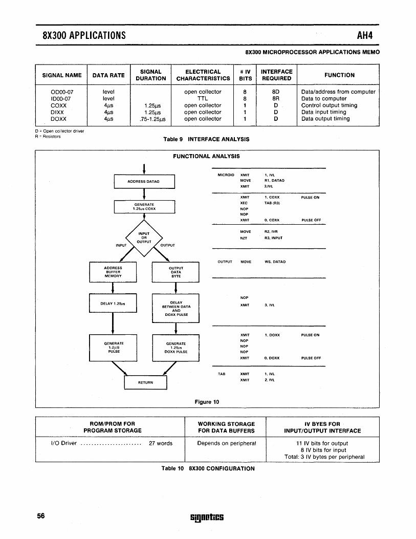
8X300 APPLICATIONS AH4
8X300 MICROPROCESSOR APPLICATIONS MEMO
SIGNAL NAME DATA RATE SIGNAL ELECTRICAL #IV INTERFACE
FUNCTION DURATION CHARACTERISTICS BITS REQUIRED
0000-07 level open collector 8 8D Data/address from computer I DOO-07 level TTL 8 8R Data to computer COXX 4J1s 1.25J1s open collector 1 D Control output timing DIXX 4J1s 1.25J1s open collector 1 D Data input timing DOXX 4J1s .75-1.25J1s open collector 1 0 Data output timing
o = Open collector driver A = Resistors
Table 9 INTERFACE ANALYSIS
FUNCTIONAL ANALYSIS
MICROIO XMIT 1.IVL
MOVE R1. DATAO
XMIT 3.IVL
XMIT 1. COXX PULSE ON
XEC TAB (R3)
NOP
NOP
XMIT O. COXX PULSE OFF
MOVE R2.IVR
NZT R3.INPUT
OUTPUT MOVE WS. DATAO
ADDRESS OUTPUT BUFFER DATA
MEMORY BYTE
NOP DELAY
XMIT 3.IVL BETWEEN DATA AND
DOXX PULSE
XMIT 1. DOXX PULSE ON
NOP GENERATE GENERATE
1.21l5 1.25/1s NOP
PULSE DOXX PULSE NOP
XMIT O.DOXX PULSE OFF
TAB XMIT 1.IVL
XMIT 2.IVL RETURN
Figure 10
ROM/PROM FOR WORKING STORAGE IV BYES FOR PROGRAM STORAGE FOR DATA BUFFERS INPUT/OUTPUT INTERFACE
110 Driver ....................... 27 words Depends on peripheral 11 IV bits for output 8 IV bits for input
Total: 3 IV bytes per peripheral
Table 10 8X300 CONFIGURATION
56 Si!lDOliC!i
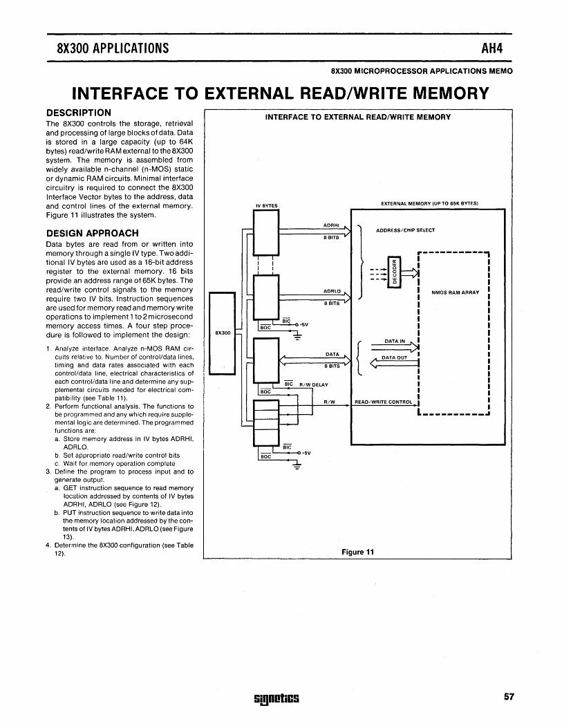
8X300 APPLICATIONS AH4
8X300 MICROPROCESSOR APPLICATIONS MEMO
INTERFACE TO EXTERNAL READ/WRITE MEMORY DESCRIPTION The 8X300 controls the storage, retrieval and processing of large blocks of data. Data is stored in a large capacity (up to 64K bytes) read/write RAM external to the 8X300 system. The memory is assembled from widely available n-channel (n-MOS) static or dynamic RAM circuits. Minimal interface circuitry is required to connect the 8X300 Interface Vector bytes to the address, data and control lines of the external memory. Figure 11 illustrates the system.
DESIGN APPROACH Data bytes are read from or written into memory through a single IV type. Two additional IV bytes are used as a 16-bit address register to the external memory. 16 bits provide an address range of 65K bytes. The read/write control signals to the memory require two IV bits. Instruction sequences are used for memory read and memory write operations to implement 1 to 2 microsecond memory access times. A four step procedure is followed to implement the design:
1. Analyze interface. Analyze n-MOS RAM circuits relative to: Number of control/data lines, timing and data rates associated with each control/data line, electrical characteristics of each control/data line and determine any supplemental circuits needed for electrical compatibility (see Table 11).
2. Perform functional analysis. The functions to be programmed and any which require supplemental logic are determined. The programmed functions are: a. Store memory address in IV bytes ADRHI,
ADRLO. b. Set appropriate read/write control bits c. Wait for memory operation complete
3. Define the program to process input and to generate output. a. GET instruction sequence to read memory
location addressed by contents of IV bytes ADRHI, ADRLO (see Figure 12).
b. PUT instruction sequence to write data into the memory location addressed by the contents of IV bytesADRHl,ADRLO (see Figure 13).
4. Determine the 8X300 configuration (see Table 12).
8X300
INTERFACE TO EXTERNAL READ/WRITE MEMORY
IV BYTES
ADRHI
8 BITS
AORlO
8 BITS
EXTERNAL MEMORY (UP TO 65K BYTES)
ADDRESS/CHIP SELECT
r-----------, I
I I NMOS RAM ARRAY I I I I I I
DATA {< DATA IN ~ ~::::::::::;;:~::;::~>: . DATA OUT II
8 BITS -
L..-__ .:.;.R/~W.:...;DELAY
R/W
!ii!lDDtiCS
I I I I I
READ/WRITE CONTROL I L __________ ..
Figure 11
57
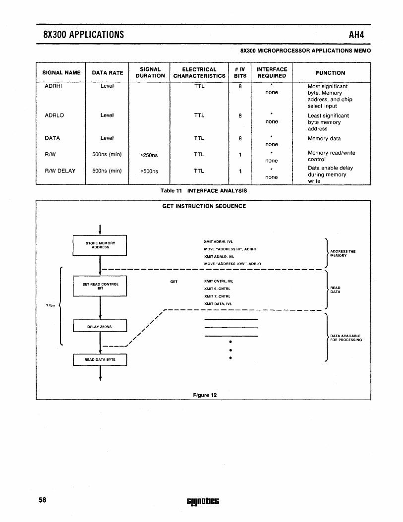
8X300 APPLICATIONS AH4
8X300 MICROPROCESSOR APPLICATIONS MEMO
SIGNAL NAME DATA RATE SIGNAL ELECTRICAL #IV INTERFACE
FUNCTION DURATION CHARACTERISTICS BITS REQUIRED
ADRHI Level TTL 8 * Most significant none byte. Memory
address, and chip select input
ADRLO Level TTL 8 " Least significant none byte memory
address
DATA Level TTL 8 .. Memory data
none
R/W 500ns (min) >250ns TTL 1 " Memory read/write
none control
R/W DELAY 500ns (min) >500ns TTL 1 .. Data enable delay
none during memory write
Table 11 INTERFACE ANALYSIS
GET INSTRUCTION SEQUENCE , STORE MEMORY XMIT ADRHI. IVL
ADDRESS MOVE "ADDRESS HI". ADRHf } ADDRESS THe
XMIT ADRLO. IVL MEMORY
MOVE "ADDRESS LOW".ADRLO ,. ---------------------------------GET XMIT CNTRL.IVt.
SET READ CONTROL BIT XMIT 5. CNTRl } READ DATA
XMIT 7. CNTRL
'''Ops ~ XMIT DATA. IVL
r-----------------------/ ""I
/ /
DELAY 250NS / /
/ ) DATA AVAILABLE /
/ • FOR PROCESSING 10.
____ J
• READ DATA BYTE • ~
l Figure 12
58 SmDOliC!i
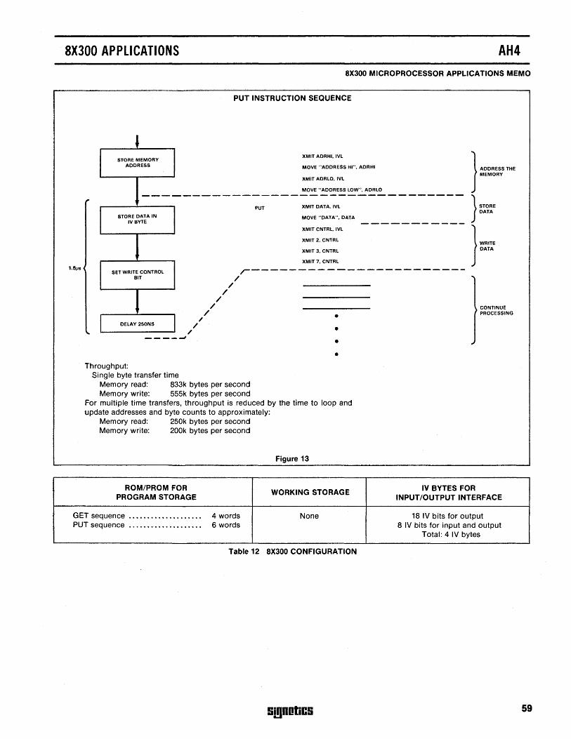
8X300 APPLICATIONS AH4
8X300 MICROPROCESSOR APPLICATIONS MEMO
, STORE MEMORY
ADDRESS
---STORE DATA IN
IV BYTE
PUT INSTRUCTION SEQUENCE
PUT
XMIT ADRHI, IVL
MOVE "ADDRESS HI", ADRHI
XMIT ADRLO, IVL
MOVE "ADDRESS LOW", ADRLO
XMIT DATA, IVL
MOVE "DATA", DATA
XMIT CNTRL, IVL
XMIT 2, CNTRL
XMIT 3, CNTRL
XMIT 7, CNTRL
}
ADDRESS THE MEMORY
}
STORE DATA
}
WRITE DATA
1.5115 SET WRITE CONTROL ,-----------------------
BIT
DELAY 250NS
____ -J
Throughput: Single byte transfer time
/
/ /
/
/ /
/ /
/
Memory read: 833k bytes per second Memory write: 555k bytes per second
• • • •
For multiple time transfers, throughput is reduced by the time to loop and update addresses and byte counts to approximately:
Memory read: 250k bytes per second Memory write: 200k bytes per second
Figure 13
ROM/PROM FOR WORKING STORAGE
PROGRAM STORAGE
GET sequence ••••••...•.•••.•..•• 4 words None PUT sequence .....•••••.•••.••••• 6 words
Table 12 8X300 CONFIGURATION
9i!100IiC!i
IV BYTES FOR
CONTINUE PROCESSING
INPUT/OUTPUT INTERFACE
18 IV bits for output 8 IV bits for input and output
Total: 4 IV bytes
59
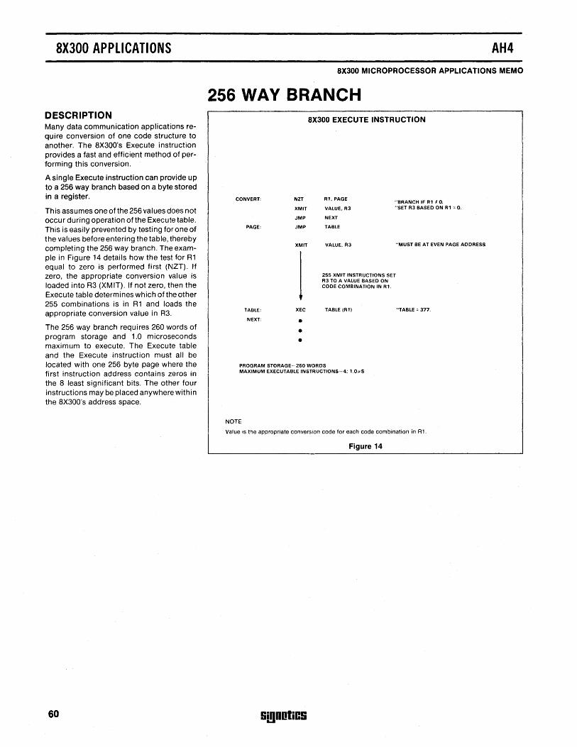
8X300 APPLICATIONS
DESCRIPTION Many data communication applications require conversion of one code structure to another. The 8X300's Execute instruction provides a fast and efficient method of performing this conversion.
A single Execute instruction can provide up to a 256 way branch based on a byte stored in a register.
This assumes one of the 256 values does not occur during operation of the Execute table. This is easily prevented by testing for one of the values before entering the table, thereby completing the 256 way branch. The example in Figure 14 details how the test for R1 equal to zero is performed first (NZT). If zero, the appropriate conversion value is loaded into R3 (XMIT). If not zero, then the Execute table determines which of the other 255 combinations is in R1 and loads the appropriate conversion value in R3.
The 256 way branch requires 260 words of program storage and 1.0 microseconds maximum to execute. The Execute table and the Execute instruction must all be located with one 256 byte page where the first instruction address contains zeros in the 8 least significant bits. The other four instructions may be placed anywhere within the 8X300's address space.
60
AH4 8X300 MICROPROCESSOR APPLICATIONS MEMO
256 WAY BRANCH
CONVERT:
PAGE:
TABLE:
NEXT:
NZT
XMIT
JMP
JMP
XMIT
I XEC
• • •
8X300 EXECUTE INSTRUCTION
R1. PAGE
VALUE. R3
NEXT
TABLE
"'BRANCH IF R1 10. "SET R3 BASED ON R1 = O.
VALUE, R3
255 XMIT INSTRUCTIONS SET R3 TO A VALUE BASED ON CODE COMBINATION IN R1.
TABLE (Rl)
"MUST BE AT EVEN PAGE ADDRESS
"TABLE = 377.
PROGRAM STORAGE-260 WORDS MAXIMUM EXECUTABLE INSTRUCTIONS-4; 1.01'S
NOTE
Value is the appropriate conversion code for each code combination in Rl.
Figure 14
SmDOliCS
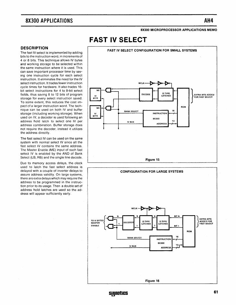
8X300 APPLICATIONS
DESCRIPTION The fast IV select is implemen!ed by adding bits to the instruction word, in increments of 4 or 8 bits. This technique allows IV bytes and working storage to be selected within the same instruction where it is used. This can save important processor time by saving one instruction cycle for each select instruction. It eliminates the need for the IV select instruction. It trades fewer instruction cycle times for hardware. It also trades 16-bit select instructions for 4 to 8-bit select fields, thus saving 8 to 12 bits of program storage for every select instruction saved. To some extent, this reduces the cost impact of a larger instruction word. The technique can be used on both IV and buffer storage (including working storage). When used on IV, a decoder is used following an address hold latch to select one IV per address combination. Buffer storage does not require the decoder, instead it utilizes the address directly.
The fast select IV can be used on the same system with normal select IV since all the fast select IV contains the same address. The Master Enable (ME) input of each fast select IV is enabled by the AND of Bank Select (LB, RB) and the single line decode.
Due to memory access delays, the clock used to latch the fast select address is delayed with a couple of inverter delays to assure address validity. On large systems, there are extra delays which may require the address to be programmed in the instruction prior to its usage. Then a double set of address hold latches are used so the address will appear sufficiently early.
AH4
8X300 MICROPROCESSOR APPLICATIONS MEMO
FAST IV SELECT FAST IV SELECT CONFIGURATION FOR SMALL SYSTEMS
ME
IV BYTE
ME
IV BYTE
TO IV BYTES{ N MASTER
ENABLE -a
MCLK --I~~-I~to--I~M)-,
ROM
BANK SELECT
IV BUS
Figure 15
CONFIGURATION FOR LARGE SYSTEMS
BANK SELECT
IV BUS
BITN
BIT 1
16 INSTRUCTION .... -r--t
BX300
Figure 16
!ii!lDOliC!i
}
EXTRA BITS ADDED FOR FAST SelECT
ROM
}
EXTRA BITS ADDED FOR FAST SELECT
61
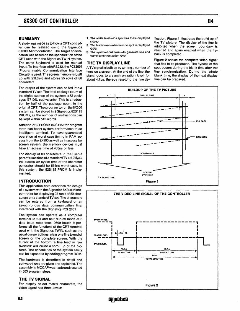
8X300 CRT CONTROLLER
SUMMARY A study was made as to how a CRT control· ler can be realized using the Signetics 8X300 Microcontroller. The target specifi· cation was based on the specification of the CRT used with the Signetics TWIN system. The same keyboard is used for manual input. To interface with RS232, the PCI2651 (Programmable Communication Interface Circuit) is used. The screen memory is built up with 21 L02-3 and stores 25 rows of 80 characters.
The output of the system can be fed into a standard TV set. The total package count of the digital section of the system is 52 packages (77 OIL equivalents). This is a reduction by half of the package count in the original CRT. The program to run the 8X300 system can be stored in 2 Signetics 82S115 PROMs, as the number of instructions can be kept within 512 words.
Addition of 2 PROMs (82S115) for program store can boost system performance to an intelligent terminal. To have guaranteed operation at worst case timing in RAM access from the 8X300 as well as in access for screen refresh, the memory devices must have an access time of 400ns or less.
For display of 80 characters in the usable part of a line time of a standard TV set (45ILs), the access (or cycle) time of the character generator should be 535ns worst case. In this system, the 82S115 PROM is implemented.
INTRODUCTION This application note describes the design of a system with the Signetics 8X300 Microcontroller for displaying 25 rows of 80 characters on a standard TV set. The characters can be entered from a keyboard or an asynchronous data communication line, interfaced with the Signetics PCI 2651.
The system can operate as a computer terminal in full and half duplex mode at 8 data baud rates (max. 9600 baud). It performs all the functions of the CRT terminal used with the Signetics TWI N, such as the usual cursor actions, clear one line to end of screen or the complete screen. With the cursor at the bottom, a line feed or row overflow will cause a scroll up of the pictures. The capabilities of the system easily can be expanded by adding program ROM.
The hardware is described in detail and software flows are given and explained. The assembly in MCCAP was made and resulted in 503 program steps.
THE TV SIGNAL For display of dot matrix characters, the video signal has three levels:
62
84
1. The white·Jevel-if a spot has to be displayed (100%)
2. The black tevel-wherever no spot 1s displayed (30%)
3. The synchronous leve'l-to generate line and frame synchronization <0%)
flection. Figure 1 illustrates the build up of the TV picture. The display of the line is inhibited when the screen boundary is reached and again enabled when the flyback is completed.
THE TV DISPLAY LINE Figure 2 shows the complete video signal that has to be produced. The flyback of the spot occurs during the blank time after the line synchronization. During the whole blank time, the display of the next display line can be prepared.
A TV signal is built up by writing a number of ·lines on a screen. At the end of the line, the signal goes to a synchronization level, for about 4.7 fJ.S, thereby resetting the line de-
...
BUILDUP OF THE TV PICTURE
DISPLAY TIME
~ .... ..- ..... -_._---
--~-........ --- ..... ---
~-- ...... F-;.,;;------+-t-- flY BACK
--.------~ ........ ......... .-. ... ----___ - ~l1NESYNC
.. ~~-------------------------~-~~ -- ~.- .........
SCREEN SIZE
---------- SCREEN OVERSCAN
---
.. " BLANK TIME
Figure 1
THE VIDEO LINE SIGNAL OF THE CONTROLLER
WHITE lEVEL ---, r----------------, I I I I I I I -.J4.7~sr- I I
BlA~'!!'~-+-i r----t----------------M SYNClEVEt. 'U I I L
18.311s J 45.7~.
BLANK TIME I DISPLAY TIME 6411S
TOTAL LINE TIME
Figure 2
9!!1DDliC9
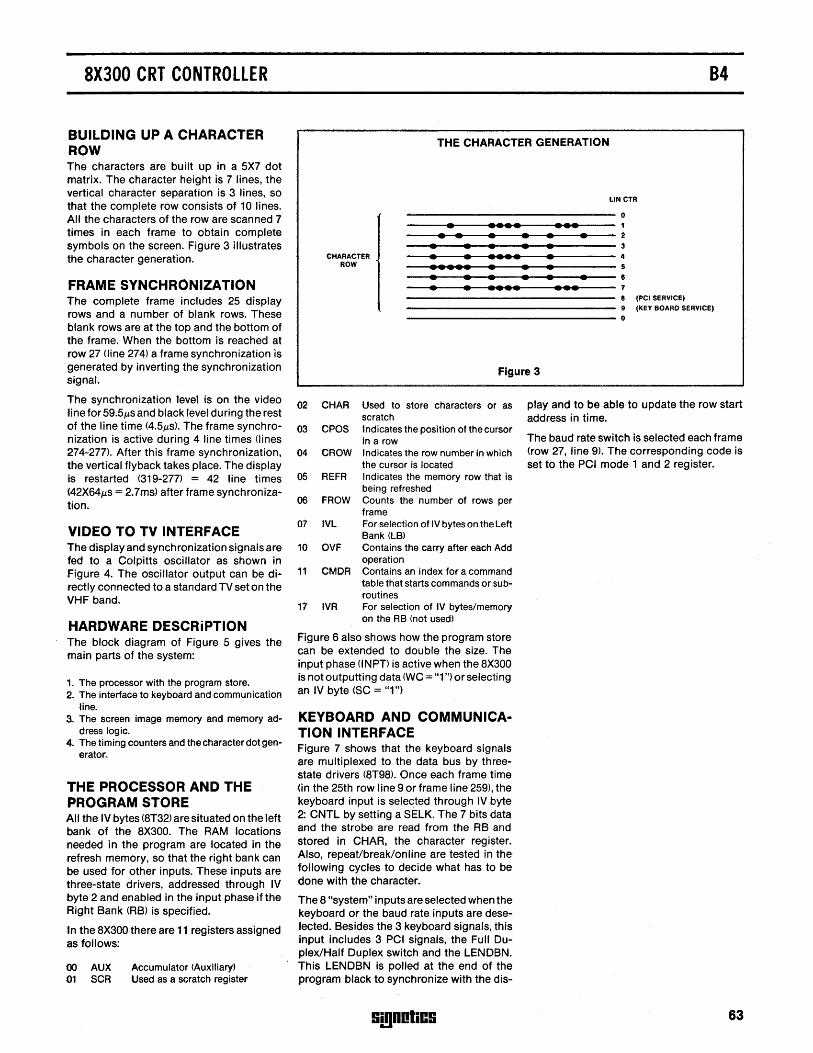
8X300 CRT CONTROLLER
BUILDING UP A CHARACTER ROW The characters are built up in a 5X7 dot matrix. The character height IS 7 lines, the vertical character separation is 3 lines, so that the complete row consists of 10 lines. All the characters of the row are scanned 7 times in each frame to obtain complete symbols on the screen. Figure 3 illustrates the character generation.
FRAME SYNCHRONIZATION The complete frame includes 25 display rows and a number of blank rows. These blank rows are at the top and the bottom of the frame. When the bottom is reached at row 27 (line 274) a frame synchronization is generated by inverting the synchronization signal.
The synchronization level is on the video tine for 59.5j.Ls and black level during the rest of the line time (4.5j.Ls). The frame synchro· nization is active during 4 line times (lines 274-277). After this frame synchronization, the vertical flyback takes place. The display is restarted (319-277) = 42 line times (42X64j.Ls = 2.7ms) after frame synchronization.
VIDEO TO TV INTERFACE The display and synchronization signals are fed to a Colpitts oscillator as shown in Figure 4. The oscillator output can be directly connected to a standard TV set on the VHF band.
HARDWARE DESCRiPTION The block diagram of Figure 5 gives the main parts of the system:
,. The processor with the program store. 2. The interface to keyboard and communication
line. 3. The screen image memory and memory ad
dress logic. 4. The timing counters and the character dot gen
erator.
THE PROCESSOR AND THE PROGRAM STORE All the IV bytes (8T32) are situated on the left bank of the 8X300. The RAM locations needed in the program are located in the refresh memory, so that the right bank can be used for other inputs. These inputs are three-state drivers, addressed through IV byte 2 and enabled in the input phase if the Right Bank (RB) is specified.
1n the 8X300 there are 11 registers assigned as follows:
00 AUX 01 SCR
Accumulator (Auxiliary) Used as a scratch register
CHARACTER ROW
THE CHARACTER GENERATION
84
Figure 3
02 CHAR
03 CPOS
04 CROW
05 REFR
06 FROW
01 lVL
10 OVF
11 CMDR
17 IVR
Used to store characters or as scratch Indicates the pOSition of the cursor in a row Indicates the row number in which the cursor is located Indicates the memory row that is being refreshed Counts the number of rows per frame For selection of IV bytes on the Left Bank (LB) Contains the carry after each Add operation Contains an index for a command table that starts commands or subroutines For selection of IV bytes/memory on the RB (not used)
Figure 6 also shows how the program store can be extended to double the size. The input phase (INPT) is active when the 8X300 is not outputting data (WC = "1") or selecting an IV byte (SC = "1")
KEYBOARD AND COMMUNICATION INTERFACE Figure 7 shows that the keyboard signals are multiplexed to the data bus by threestate drivers (8T98). Once each frame time (in the 25th row line 9 or frame line 259), the keyboard input is selected through IV byte 2: CNTL by setting a SELK. The 7 bits data and the strobe are read from the RB and stored in CHAR, the character register. Also, repeat/break/online are tested in the following cycles to decide what has to be done with the character.
The 8 "system" inputs are selected when the keyboard or the baud rate inputs are deselected. Besides the 3 keyboard signals, this input includes 3 PCI signals, the Full Duplex/Half Duplex switch and the LENDBN. This LENDBN is polled at the end of the program black to synchronize with the dis-
Gi!)notiCG
play and to be able to update the row start address in time.
The baud rate switch is selected each frame (row 27, line 9), The corresponding code is set to the PCI mode 1 and 2 register.
63
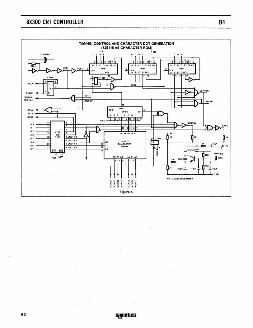
8X300 CRT CONTROLLER
12.2SMHz
'/2 7474
XCLK
XCLKN
CHRDlS TO FIG. 7
SELC
SELK
BORT
16 IVO
17 IV1
18 IV2 8T32 19 IV3 IVB
20 CHTL IV4
21 IVS
22 IV6
IV7 23
SiC BOC
10
VCC
64
TIMING, CONTROL AND CHARACTER DOT GENERATION (82S115 AS CHARACTER ROM)
~ 7
1 0 0 1 o 0 0 0
14 10 9 8 7
05 04 03 02 01
.;- 112 1 0 0 1
t-----------~-4-------2-i3 A2 82S11S CHARACTER
PROM
Q '/2 7474
9
1 LNCTR 0 22 A1
21 AO
c :il w :il
A8 A7 A6 AS A4 A3
6 5 4 3 2 1
'" '" ;g '" CD .... C C C C c :il :il :il :il ~ :il w w w w w :il :il :il :il :il :il
Figure 4
9i!1DOliC!i
12 11 o T
'" ~ o
..---------.... ------.... - ..... --~ GNO
R.F. OSCILLATOR-MIXER
84
1K
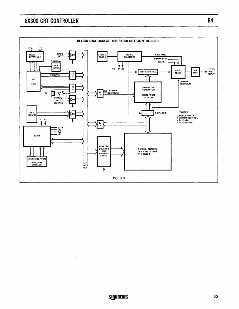
8X300 CRT CONTROLLER
BLOCK DIAGRAM OF THE 8X300 CRT CONTROLLER
DATA BUS
TO X1 X2
SYSTEM CONTROLS
Figure 5
Gi!lDOliCS
LINE SYNC
FRAME SYNC
BLANK
CHARACTER GENERATOR
82S115 PROM 2513 ROM
8-BIT LATCH
REFRESH MEMORY 2K x 7 STATIC RAM 14 x 21L02-3
VIDEO MIXER
CURSOR INVERSION
IV BYTES
1 .• MEMORY DATA 2. SYSTEM CONTROL 3. PCI DATA 4. PCI CONTROL
84
TO TV VHF INPUT
65
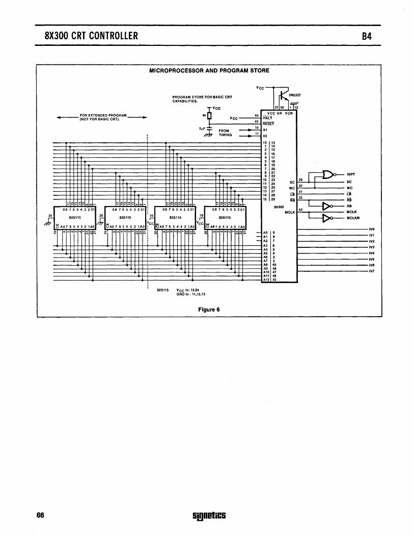
8X300 CRT CONTROLLER
MICROPROCESSOR AND PROGRAM STORE
.. rNO~T E:ci~~~~~t~~~~AM ---.
i I
I
I
I
I
I
I
I
I
I
..... CD "'~ 0
~'" CD .... ..... CD "'~ ~mco,...:
08 7 6 5 4 3 201 087654 3201 !
)- 82S115 i 82S115 '~
~A87654321AO IIJ rce UA87 6 5 4 3 2 lAO
~j CD'" .. '" "'~ M"'~
~1 CD'" <tM N~ MN ~I ",,,,,,,
"'''' "Ii
: I
I
I
I
I
I I
66
PROGRAM STORE FOR BASIC CRT CAPABILITIES.
·~VCC
4k I) VCC
7P:% FROM
TIMING
..... CD "'~ I~", CD .... ~~ "' .. ~ 0'1 col,..., 08 7 6 5 4 3 201 08 7 6 5 4 3 201
82S115 ~ 112S115
I~A8 7 6 5 4 3 2 1 AO Vee
I~A1I7654321AO
~1 CD'" ~M "'~ "''''~ "'''IN ~l
82S115 Vce 10: 18.24 GND 10: 11.12.13
CD'"
Figure 6
~'"
!i(gDOliC9
"'~ "'''' ... ",,,,N
VCC
,~~m 37 50 I~
44 VCC VR VCR
HALT 43
RESET 10
Xl 11
X2
10 13 1 14 2 15 3 16 4 17 5 18 6 19 7 20 8 21 9 22
10 23 29 11 24 SC
30 12 25 WC 13 27
Ui 31
14 28 15 29 iijj
32
IIX300
MCLK 42
- AD 9 - Al II - A2 7
A3 8 A4 5 AS 4 A6 3 A7 2 All 49 A9 48 Al0 47 All 4/l A12 45
-~'NPT 1 sc
WC
[8
~: MCLK
L-[:>o- MCLKN
84
IVO
IVl
IV2
IV3
IV4
IV5
IV/l
IV7
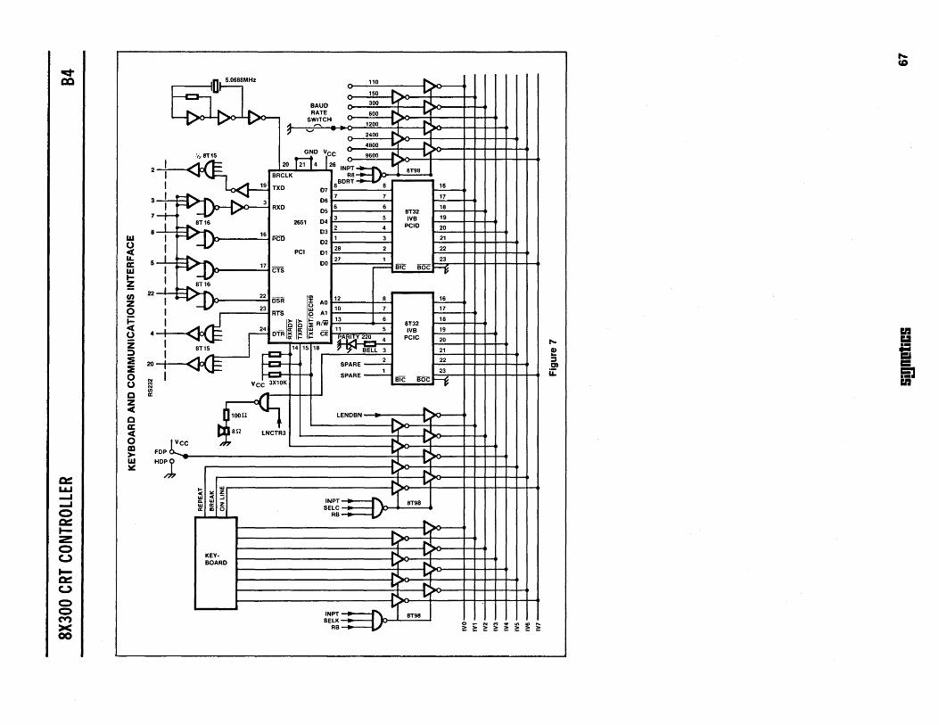
IIIIdco
0::: YJ ..... ..... o 0::: tZ o (..)
to::: (..)
o o M >< 00
w o CC IL. a: W I-~ en z o i= CC g Z :l ::E ::E o o c z CC c a: CC o III >0-W ~
110 ~D' 5.0688MHz
BAUD RATE
~ 150 ~ 300
S~CH
'-'
GND
7 H 8T32
'" 1 IVB RXD 2651 ~:~; _
03 - 1 _
"""'-----. PCD 02 28 ~~C'D BIC
t'l;I 01
DO 127
JOo------t CTS
JOo----~ DSR AO t1.;.;2~ __ +.-;;-t _ 10
r--------tRTS A1t-----r--; 13
11
~ VCC 3X10K I/) a:
~loon -<{I:'" 8n - ~
FOP lNCTR3
KEYBOARD
8T32 IVB
PCIC
BIC
16
17
18
~ 17
I I I I I I I o ~ N (') "" &I) co ,.... ~ ~ ~ ~ ~ ~ ~ ~
r-Q) .. :::I g)
~
..... CQ
UlII 1:.1 .-... 1:1 = 5l UlII
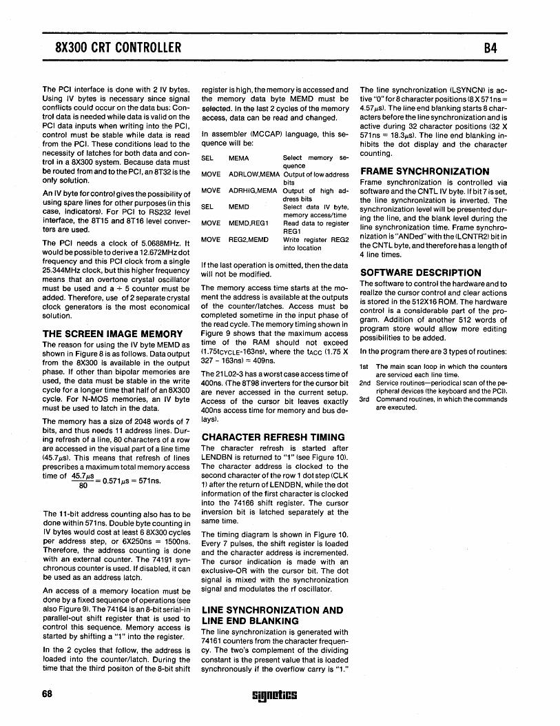
8X300 CRT CONTROLLER
The PCI interface is done with 2 IV bytes. Using IV bytes is necessary since signal conflicts could occur on the data bus: Control data is needed while data is valid on the PCI data inputs when writing into the PCI, control must be stable while data is read from the PCI. These conditions lead to the necessity of latches for both data and control in a 8X300 system. Because data must be routed from and tothe PCI, an 8T32 is the only solution.
An IV byte for control gives the possibility of using spare lines for other purposes (in this case, indicators). For PCI to RS232 level interface, the 8T15 and 8T16 level converters are used.
The PCI needs a clock of 5.0688MHz. It would be possible to derive a 12.672MHz dot frequency and this PCI clock from a single 25.344MHz clock, but this higher frequency means that an overtone crystal oscillator must be used and a + 5 counter must be added. Therefore, use of 2 separate crystal clock generators is the most economical solution.
THE SCREEN IMAGE MEMORY The reason for using the IV byte MEMD as shown in Figure 8 is as follows. Data output from the 8X300 is available in the output phase. If other than bipolar memories are used, the data must be stable in the write cycle for a longer time that half of an 8X300 cycle. For N-MOS memories, an IV byte must be used to latch in the data.
The memory has a size of 2048 words of 7 bits, and thus needs 11 address lines. During refresh of a line, 80 characters of a row are accessed in the visual part of a line time (45.7J.Lsl. This means that refresh of lines prescribes a maximum total memory access
time of 45.7,us = 0571 = 571 80 . J.Ls ns.
The 11-bit address counting also has to be done within 571 ns. Double byte counting in IV bytes would cost at least 6 8X300 cycles per address step, or 6X250ns = 1500ns. Therefore, the address counting is done with an external counter. The 74191 synchronous counter is used. If disabled, it can be used as an address latch.
An access of a memory location must be done by a fixed sequence of operations (see also Figure 9). The 74164 is an 8-bit serial-in parallel-out shift register that is used to control this sequence. Memory access is started by shifting a "1" into the register.
In the 2 cycles that follow, the address is loaded into the counter/latch. During the time that the third positon of the 8-bit shift
68
register is high, the memory is accessed and the memory data byte MEMD must be selected. In the last 2 cycles of the memory access, data can be read and changed.
In assembler (MCCAP) language, this sequence wi II be:
SEL MEMA Select memory sequence
MOVE ADRLOW,MEMA Output of low address bits
MOVE ADRHIG,MEMA Output of high address bits
SEL MEMD Select data IV byte. memory access/time
MOVE MEMD,REG1 Read data to register REG1
MOVE REG2,MEMD Write register REG2 into location
If the last operation is omitted, then the data will not be modified.
The memory access time starts at the moment the address is available at the outputs of the counter/latches. Access must be completed sometime in the input phase of the read cycle. The memory timing shown in Figure 9 shows that the maximum access time of the RAM should not exceed (1.75tcYCLE-163ns), where the tACC (1.75 X 327 - 163ns) = 409ns.
The 21 l02-3 has a worst case access ti me of 400ns. (The 8T98 inverters for the cursor bit are never accessed in the current setup. Access of the cursor bit leaves exactly 400ns access time for memory and bus delaysl.
CHARACTER REFRESH TIMING The character refresh is started after lENDBN is returned to "1" (see Figure 10). The character address is clocked to the second character of the row 1 dot step (ClK 1) after the return of lENDBN, while the dot information of the first character is clocked into the 74166 shift register. The cursor inversion bit is latched separately at the same time.
The timing diagram is shown in Figure 10. Every 7 pulses, the shift register is loaded and the character address is incremented. The cursor indication is made with an exclusive-OR with the cursor bit. The dot signal is mixed with the synchronization signal and modulates the rf oscillator.
LINE SYNCHRONIZATION AND LINE END BLANKING The line synchronization is generated with 74161 counters from the character frequency. The two's complement of the dividing constant is the present value that is loaded synchronously if the overflow carry is "1."
Smnotics
84
The line synchronization (lSYNCN) is active "0" for 8 character positions (8 X 571 ns = 4.57 J.Ls). The line end blanking starts 8 characters before the line synchronization and is active during 32 character positions (32 X 571ns = 18.3J.Lsl. The line end blanking inhibits the dot display and the character counting.
FRAME SYNCHRONIZATION Frame synchronization is controlled via software and the CNTl IV byte. If bit 7 is set, the line synchronization is inverted. The synchronization level will be presented during the line, and the blank level during the line synchronization time. Frame synchronization is "ANDed" with the (lCNTR2) bit in the CNTl byte, and therefore has a length of 4 line times.
SOFTWARE DESCRIPTION The software to control the hardware and to realize the cursor control and clear actions is stored in the 512X16 ROM. The hardware control is a considerable part of the program. Addition of another 512 words of program store would allow more editing possibilities to be added.
In the program there are 3 types of routines:
1st The main scan loop in which the counters are serviced each line time.
2nd Service routines-periodical scan of the peripheral devices (the keyboard and the PCI>.
3rd Command routines, in which the commands are executed.
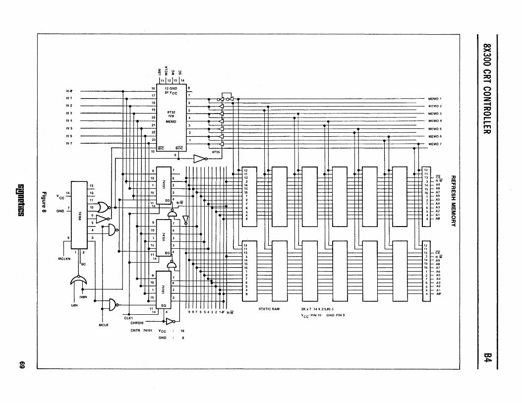
." cS' c Ci1 co
IV.8'
IV 1
IV 2
IV 3
IV4
IV 5
IV6
IV 7
~
14 -7
GND -~
i
9
[~[ SC
MC
rr T
IV3N
lali
13 r-
12 -11
~ ..-/"
~ i-- • 4
3 r-
,--
P> MClK
-'11113115114
16 12GND
17 24 VCC
18
19 8T32
20 IVB
MEMO 21
22
23
BiC BOc 10
91
9r---7
t--10 6
~ ~ 1 2
15 3
EG 4
1~4I:::~ R/W
~ 9 7
10 6 r- t--
~ 1 2 >--
15 3
14 ~~ 9
7
10 6 ... t--~ 1 2
.... r-15 3
t--EG
11~ 14 ~
ClK1
CHRDlS
CNTR 74191 VCC 16
GND
4
8 r-
r-:1, 7
T ..., ~ 6
5 T
4 T
3 T
2 1 -r' ..)
1 l
T I"
8T95 I ."..
r--~ 12
4r-- 11 13
~r- 3 14 15 16 1 2 7 6 5 4 8
'---
~ 12
'-- 11 13
~ 3 14 15 16 1 2 7 6 5 4 8
'---
9 8 7 6 5 4 3 2 l-EY Riw
r--- r--- r--t-
~ ~t- 4 t-r-I- r-t-t- r- t--r-r-I- r-t-t- r- t--r-r-I- r-t- r- t--t-r-I- r-t- r- r-r-- - I-- ~ - - - I--r-r- I-- - t--r-r- I-- - t--r-r- I-- I-- t--t-r- t-- t-- t--t-r- f-- f-- t- t--t-t-- I-- I-- t- t--t-
'--- ---- '---
..--- - -..... '- l-
'-- '-- 0.- '--
r---- r--- r--- -r---- r--- r--- r----t--- r--- r--- r----t--- r--- r--- r----r---- r--- - -r---- r--- - -t--- r--- r--- r----t--- r--- r--- t---t--- r--- r--- r----t--- t--- r--- t---t-- t--- t--- t---r--- t--- t--- t---
"-- ---- '---
STATIC RAM 2K x 7: 14 X 21le2-3
Vce: PIN 10 GNO: PIN 9
r--- r---
r- t-r-r- t--f-r-r- r-r-t--r- t--f-r-r- r-r--- r--I- t--f--I- -t--I- -t-1--1- r-t-r-t- r-t-t--t- r-t-r-I- t--
""---- ----- :---
'-- '--
r---- r----r---- r----t--- r----t--- r----r-- r---r-- r---r---- r---t--- r---r--- r---t--- t---t--- t---r--- t---
'--- '"---
MEMO
MEM 02
MEM 03
MEM 04
MEM 05
MEM 06
MEM 07
r--12 11 13 r-
3 r-14 t-15 r-16 -1 -2 -7 -6 t-5 r-4t-8t-
'--
~
12 II 13 t-
3 t-14 t-15 t-16 r-1 I-2 I-7 I-6 I-5 t-4 t-8t-
"""-
Ce RW A9 AS A7 AS AS A4 A3 A2 Al M
Ce RW A9 AS A7 AS AS A4 A3 A2 A1 Aff
00 >< W o o n ::c --I
n o :z --I ::c o rrrr1 ::c
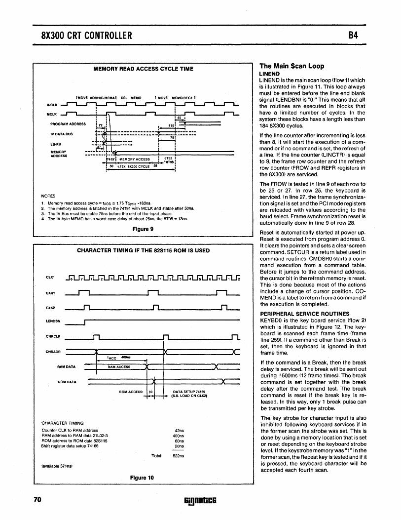
8X300 CRT CONTROLLER
MEMORY READ ACCESS CYCLE TIME
IMOVE ADRHIG,MEMAI SEt. MEMO I MOV! MEMD,REG1'
1 t
MCLK ~------~~~-----!~~~~--------~ ~
PROGRAM ADDRESS , 115i :J~I~===== ................................ -*-=::t---'- ...... .--_................. 75
1 --_ •••• IV DATA BUS
I--i I I I I
lB/RB
MEMORY ADDRESS
I I I -....... :.- .. ;.-.~.========+===~======== ···----·t--~ I
174191: MEMORY ACCESS : ~TT32: ., I .895
: 50 1.75X 8X300 CYCLE 38
NOTES
1. Memory read access cyc1e = tACC ~ 1]5 TCycle -163n8 2. The memory address is latched in the 74191 with MCLK and stable after SOns. 3. The IV Bus must be stable 75ns before the end of the input phase. 4. The IV byte MEMO has a worst case delay of about 25n5, the 8T95 :0 13ns.
Figure 9
CHARACTER TIMING IF THE 82S115 ROM IS USED
ClK1
CARl ~~ __________ ~rI~ ____________ r-L--
ClK2 ----11~ _____________ n~ _____________ rL__
LEND8N
CHRCLK n
CHRADR
tACC 40On5
RAM DATA
ROM DATA
CHARACTER TIMING
Counter CLK to RAM address RAM address to RAM data 21 L02-3 ROM address to ROM data 828115 Shift register data setup 74166
{available 571ns)
70
RAM ACCESS
ROM ACCESS: 60
Total
Figure 10
n-n.. ' ~
DATA SETUP 74166 (S.R_ LOAD ON CLK2)
42ns 400ns 60ns 20ns
522ns
)(
SmnOliCS
-JL
-.J(
The Main Scan Loop LINEND
84
LlNEND is the main scan loop (flow 1.) which is illustrated in Figure 11. This loop always must be entered before the line end blank signal (LENDBN) is "0." This means that all the routines are executed in blocks that have a limited number of cycles. In the system these blocks have a length less than 184 8X300 cycles.
If the line counter after incrementing is less than 8, it will start the execution of a command or if no command is set, the refresh of a line. It the line counter (LINCTR> is equal to 9, the frame row counter and the refresh row counter (FROW and REFR registers in the 8X300> are serviced.
The FROW is tested in line 9 of each row to be 25 or 27. In row 25, the keyboard is serviced. In line 27, the frame synchronization signal is set and the PCI mode registers are reloaded with values according to the baud select. Frame synchronization reset is automatically done in line 9 of row 28.
Reset is automatically started at power up. Reset is executed from program address O. It clears the pointers and sets a clear screen command. SETCUR is a return label used in command routines. CMDSRO starts a command execution from a command table. Before it jumps to the command address, the cursor bit in the refresh memory is reset. This is done because most of the actions include a change of cursor position. COMEND is a label to return from a command if the execution is completed.
PERIPHERAL SERVICE ROUTINES KEYBDO is the key board service (flow 2) which is illustrated in Figure 12. The keyboard is scanned each frame time (frame line 259>' If a command other than Break is set, then the keyboard is ignored in that frame time.
If the command is a Break, then the break delay is serviced. The break will be sent out during ±500ms (12 frame times). The break command is set together with the break delay after the command test. The break command is reset if the break key is released. In this way, only 1 break pulse can be transmitted per key strobe.
The key strobe for character input is also inhibited following keyboard services if in the former scan the strobe was set This is done by using a memory location that is set or reset depending on the keyboard strobe level. If the keystrobe memory was "1" in the formerscan, the Repeat key is tested and if it is pressed, the keyboard character will be accepted each fourth scan.
8X300 CRT CONTROLLER
DISABLE CHARACTER CNTR
lNCREMENT LINE CNTR (LINCTR)
UPDATE ROW START ADDRESS
ENABLE CHARACTER CNTR
FLOW 1-MAIN SCAN LOOP
RESET PARITY RESET FROW REG, RESET REFR REG. RESET CNTL-BYTE
Figure 11
9i!1001iC9
COMMAND JMP TABLE: SETCUR SETBEL CURSLE CURSRI CURSUP CURSDW CURSHe' LNFDe' CLRSCR CLREOS CLR LIN CLR LNS CBLOCK
84
71
72
8X300 CRT CONTROLLER
yes
no
SET CMDR TO CHARACTER SERVo
FLOW 2-KEYBOARD SERVICE
SET PCI CMD: BREAK
SET DELMEM TO 12
.8'TO PCIMEM
Figure 12
S!!IDOliCS
84
yes
no
no
8X300 CRT CONTROLLER
At the end of the keyboard service, the online and half duplex/full duplex switches are tested. If the system is not online, then the PCI data memory PCIMEN (character to be transmitted by the PCI) is reset and the command for the character service routine is set.
If the system is online, then the character to be transmitted from the keyboard is loaded in the PCIMEN location and the FOP/HOP switch is tested. When online, the character service command will be set only in case of half duplex. In full duplex, characters are serviced only if received via the PCI from the data communications line.
PCISER The PCI service (flow 7) is shown in Figure 13. It starts with a test on the command register. The CMOR will be set only ifone of the longer command routines has not been completed.
This type of routine starts with a reset ofthe OIR (data terminal ready signal). The system that provides signals will either test the OIR sig nal or must wait automatically after sending these commands. Characters received while a command is still set will result in an overrun error.
If the transmitterofthe PCI is ready, the new character to be transmitted is loaded via SCR (an 8X300 register). If the receiver is ready, the data is read into the CHAR register of the 8X300. The status of the PCI is tested for transmission errors. The PCI commands transmitter enable and receiver enable are set if their respective ready signals where active and a non-zero character is transmitted and/or received.
PCIINI PCI initialization (flow 7) is done every 27th row at line 9. The mode one register setting is independent of the switch setting. For mode two register setting, the baud rate switch is tested and the accessory code is merged with the fixed part of the code. Also in this routine, the bell delay is serviced and the bell signal is controlled.
COMMAND ROUTINES Command routines are started from the main scan loop with an indexed jump. The command register CMOR is the index ofthe command that is set. The commands start with a reset of the cursor bit and ends with reset of the command register if completed (COMENDl and a restore of the cursor bit (SETCURl.
CHRSRO CHRSRO is the character service routine (flow 3) shown in Figure 14. The command to run this routine is set by the keyboard input or the PCI input routines. The charac-
84
FLOW 7-PCI SERVICE AND INITIATION + BELL SERVICE
Figure 13
ter to be serviced is located in the CHAR register. The routine compares CHAR with the escape code.
If CHAR is an ESC, then it sets the ESC memory location and jumps out of routine. If no ESC was detected, the ESC memory is reset. The character is compared with an escape command table if the escape memory was set in the previous chapter service. If the character is not found in the ESC charactertableafter an escape, it will be ignored. When a control character to be serviced and also the previous character are both not the
Gi,gnotiCG
escape code, then the CHAR contents is . compared with the control character table. When a control character is found the accessory command is set. If not found, the character is a normal character to be displayed and it will be loaded in the screen memory on the cursor position.
The routine then finishes with an increment of the cursor pOSition. Possible row end actions, like conditions set of bell delay, carriage return and line feed actions will also be done.
73
8X300 CRT CONTROLLER 84
FLOW 3-CHARACTER SERVICE
Figure 14
74 SmnOliCS
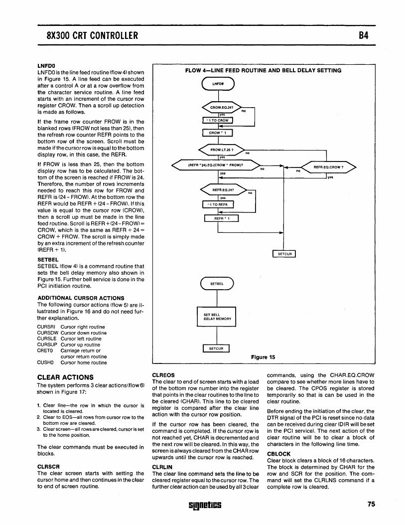
8X300 CRT CONTROLLER
LNFDO LNFOO is the line feed routine (flow 4) shown in Figure 15. A line feed can be executed after a control A or at a row overflow from the character service routine. A line feed starts with an increment of the cursor row register CROW. Then a scroll up detection is made as follows.
If the frame row counter FROW is in the blanked rows (FROW not less than 25), then the refresh row counter REFR points to the bottom row of the screen. Scroll must be made if the cu rsor row is eq ual to the bottom display row, in this case, the REFR.
If FROW is less than 25, then the bottom display row has to be calculated. The bottom of the screen is reached if FROW is 24. Therefore, the number of rows increments needed to reach this row for FROW and REFR is (24 - FROW). At the bottom row the REFR would be REFR + (24 - FROW>. If this value is equal to the cursor row (CROW), then a scroll up must be made in the line feed routine. Scroll is REFR + (24 - FROW) = CROW, which is the same as REFR + 24 = CROW + FROW. The scroll is simply made by an extra increment of the refresh counter (REFR + 1>'
SETBEL SETBEL (flow 4) is a command routine that sets the bell delay memory also shown in Figure 15. Further bell service is done in the PCI initiation routine.
ADDITIONAL CURSOR ACTIONS The following cursor actions (flow 5) are illustrated in Figure 16 and do not need further explanation.
CURSRI Cursor right routine CURSDW Cursor down routine CURSLE Cursor left routine CURSUP Cursor up routine CRETO Carriage return or
cursor return routine CUSHO Cursor home routine
CLEAR ACTIONS The system performs 3 clear actions(flow6) shown in Figure 17:
1. Clear line-the row in which the cursor is located is cleared.
2. Clear to EOS-all rows from cursor row to the bottom row are cleared.
3. Clear screen-all rows are cleared, cursor is set to the home position.
The clear commands must be executed in blocks.
CLRSCR The clear screen starts with setting the cursor home and then continues in the clear to end of screen routine.
84
FLOW 4-LINE FEED ROUTINE AND BELL DELAY SETTING
(REFR +24).EQ.(CROW + FROW)? no no
~ ________ ~ _____ ---Jyes
SET BELL DELAY MEMORY
Figure 15
CLREOS The clear to end of screen starts with a load of the bottom row number into the register that points in the clear routines to the line to be cleared (CHAR). This line to be cleared register is compared after the clear line action with the cursor row position.
If the cursor row has been cleared, the command is completed. If the cursor row is not reached yet, CHAR is decremented and the next row will be cleared. In this way, the screen is always cleared from the CHAR row upwards until the cursor row is reached.
CLRLIN The clear line command sets the line to be cleared register equal to the cursor row. The further clear action can be used by all 3 clear
!iillDOliC!i
commands, using the CHAR.EQ.CROW compare to see whether more lines have to be cleared. The CPOS register is stored temporarily so that is can be used in the clear routine.
Before ending the initiation of the clear, the OTR Signal of the PCI is reset since no data can be received during clear (OIR will beset in the PCI service). The next action of the clear routine will be to clear a block of characters in the following line time.
CBLOCK Clear block clears a block of 16 characters. The block is determined by CHAR for the row and SCR for the position. The command will set the CLRLNS command if a complete row is cleared.
75
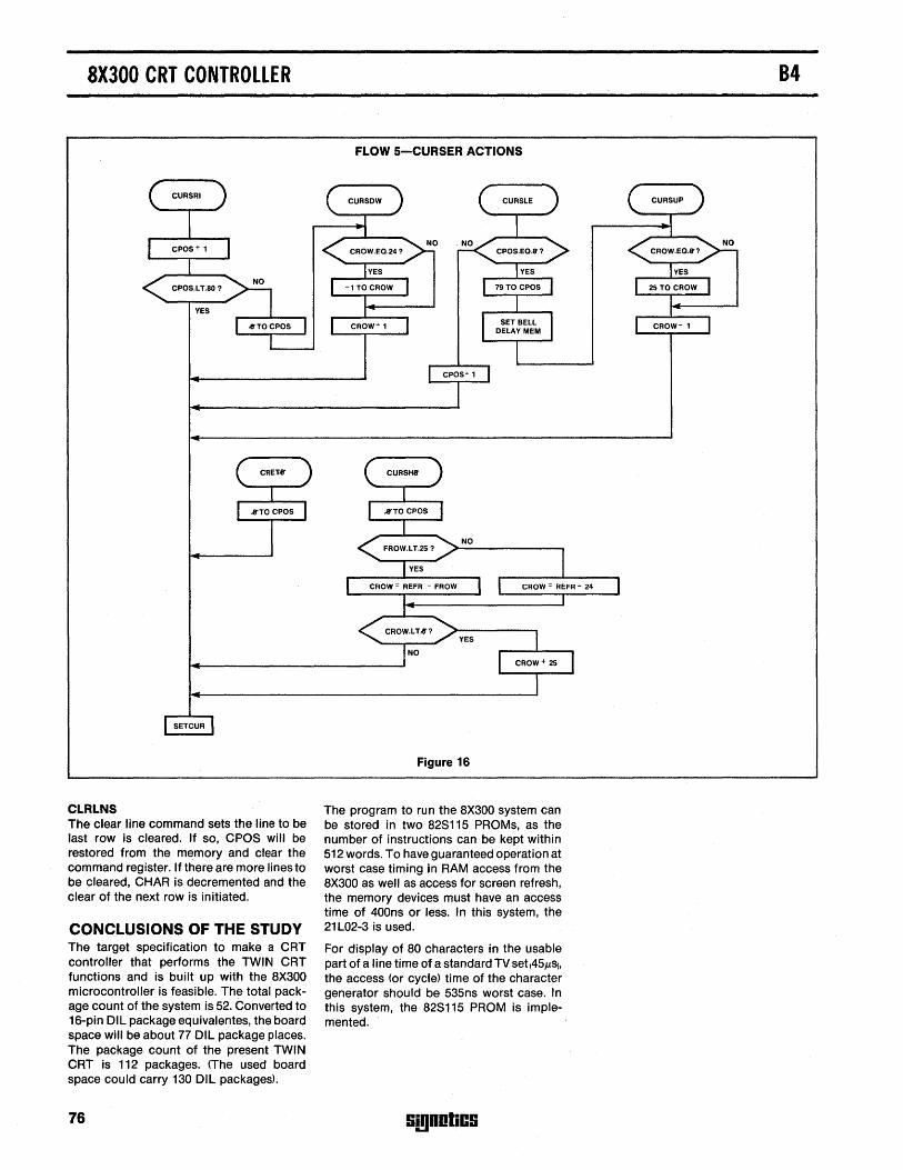
8X300 CRT CONTROLLER
CLRLNS The clear line command sets the line to be last row is cleared. If so, CP08 will be restored from the memory and clear the command register. If there are more lines to be cleared, CHAR is decremented and the clear of the next row is initiated.
CONCLUSIONS OF THE STUDY The target specification to make a CRT controller that performs the TWIN CRT functions and is built up with the 8X300 microcontroller is feasible. The total package count of the system is 52. Converted to 16-pin OIL package equivalentes, the board space will be about 77 OIL package places. The package count of the present TWIN CRT is 112 packages. (The used board space could carry 130 OIL packages).
76
FLOW 5-CURSER ACTIONS
Figure 16
The program to run the 8X300 system can be stored in two 828115 PROMs, as the number of instructions can be kept within 512 words. To have guaranteed operation at worst case timing in RAM access from the 8X300 as well as access for screen refresh, the memory devices must have an access time of 400ns or less. In this system, the 21 L02-3 is used.
For display of 80 characters in the usable part of a line time of a standard TV set (45jLs), the access (or cycle) time of the character generator should be 535ns worst case. In this system, the 828115 PROM is implemented.
Si!lDDliC!i
84
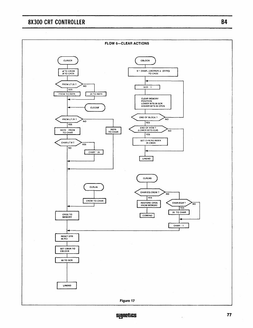
8X300 CRT CONTROLLER
CPOS TO MEMORY
FLOW 6-CLEAR ACTIONS
Figure 17
Si!lDotiCS
(017H»
CLEAR MEMORY POSITION: LOWER BITS IN SCR HIGHER BITS IN CPOS
END OF BLOCK?
YES
END OF ROW?
NO
(LOWER BITS.EQ.-6') NO
84
77
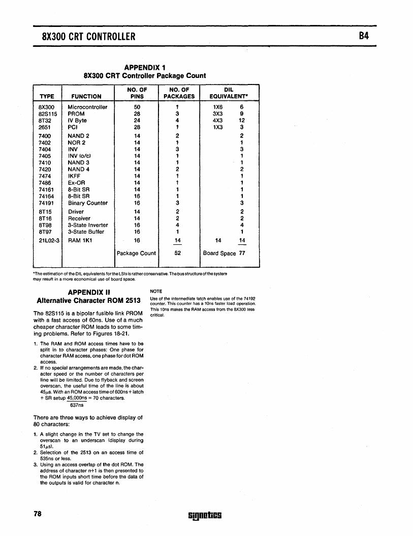
8X300 CRT CONTROLLER
APPENDIX 1 8X300 CRT Controller Package Count
NO. OF NO. OF OIL TYPE FUNCTION PINS PACKAGES EQUIVALENT-
8X300 Microcontrol/er 50 1 1X6 6 82S115 PROM 28 3 3X3 9 8T32 IV Byte 24 4 4X3 12 2651 PCI 28 1 1X3 3
7400 NAND 2 14 2 2 7402 NOR2 14 1 1 7404 INV 14 3 3 7405 INV (o/c) 14 1 1 7410 NAND 3 14 1 1 7420 NAND 4 14 2 2 7474 IKFF 14 1 1 7486 Ex-OR 14 1 1 74161 8-Bit SR 14 1 1 74164 8-Bit SR 16 1 1 74191 Binary Counter 16 3 3
8T15 Driver 14 2 2 8T16 Receiver 14 2 2 8T98 3-State Inverter 16 4 4 8T97 3-State Buffer 16 1 1
21 L02-3 RAM 1Kl 16 14 14 14 - -Package Count 52 Board Space 77
"The estimation of the DIL equivalents for the LSls is rather conservative. The bus structure ofthe system may result in a more economical use of board space.
APPENDIX II Alternative Character ROM 2513
The 82S115 is a bipolar fusible link PROM with a fast access of 60ns. Use of a much cheaper character ROM leads to some timing problems. Refer to Figures 18-21.
1. The RAM and ROM access times have to be split in to character phases: One phase for character RAM access, one phase for dot ROM access.
2. If no special arrangements are made, the character speed or the number of characters per line will be limited. Due to flyback and screen overscan, the useful time of the line is about 45~s. With an ROM access time of 600ns + latch + SR setup 45,ooons = 70 characters.
637ns
There are three ways to achieve display of 80 characters:
1. A slight change in the TV set to change the overscan to an underscan (display during 51~s).
2. Selection of the 2513 on an access time of 535ns or less.
3. Using an access overlap of the dot ROM. The address of character n+1 is then presented to the ROM inputs short time before the data of the outputs is valid for character n.
78
NOTE
Use of the intermediate latch enables use of the 74192 counter. This counter has a 10ns faster load operation. This 10ns makes the RAM access from the 8X300 less critical.
Si!lDOliCS
84
TIMING, CONTROL AND CHARACTER DOT GENERATION
A.12.25MH21
e.l0.99MH21 , 0 0
A. 0 0 0 0
9. 0 0
:Or
®C:---C»~ 1,1.1.1,1,,1, r.- I, 1.1.1,1"" A B C o ET EP LO A B C 0 ET
CLK1 2 74161 2 14161 CLK ~ ClK
Re A2 B2 C2 02 RC
III 11 15
',1474
~ "{>-
5~~ Q D 12
XCLK ... - Q 0 7474 11
~ CLK2 3
CLK
XCLI<N .. ~ Q ~ -CHRCLK
15 - 7
~l LDN
S~LC ClK 13 74166 Q H SELf<
1 BDRT A B C D ~ F G H
11 2 3 4 5 10 li 18 J 14 GND -16 8
IVir_ 17 7
r--1F IV1_ 8 7 6 5 4 18 6
IV2-19 8T32 5 05 04 03 02 01
IV3- IVB 20 CNTL 4 16
IV4- A3 21 3 15 2513 ROM
IV5_
I A2
22 2 14 G IV6-
I Al N 23 1 A9 A8 A7 A6 AS A4 0 CE
IV7-SiC BOC ~24 r2 [1
22 21 20 19 18 17 ~l
\10 J: • S -11
Vce -5 CLK2 I
BELLFR. , , 12 ,10 7 5 2 19 2 7 10 115
I 9 745174 745175
~13 flf r t3 r r f2113
NOTES 1. 2513 access time == 535ns 2. Screen overscan changed in TV set; display time 51tls per line.
Figure 18
EP
Z III Q Z w ...
9
LO
~
A. ,
e. ,
o 0 ,
o 0
I I I I , , , I
... ,..---- -112
... ,.1---- -100
I
.,~ 3 4 5 6 10 I 7 9 I B3
I C3 r A B C o ET EP Lo
74161 I C2_ CLK I 02-
A3 B3 C3 03 RC I B3-14 13 12 "Lt>-- C3- 8 I
I 02- ~ L _______ I ---------, I {»- '\.... LSYNCN t
I I ./ 0 I I t I
I ~l J
LEND BN I I ./ l 1.. _____________ ____ J
:jD-~NAL
)~ -r- Vce o lK6 911<6
21< I 4.7pF - Il ~
~=i= -t _ r.t.
47PF=~ 1]10K JVCC 4K 100 •. ,
4~
I] 2K I) 331<
"'FT .MY f'~' GND
R.F. OSCILLATOR-MIXER
t'"
"' Z o III Z
'" Ul -< Z () Z
4K2
00 >< W C> C>
n ::a -t n o :z -t ::a o rr-
'"" ::a
8X300 CRT CONTROLLER 84
RAM AND ROM TIMING DIAGRAM
CLK1
CAR1
CLK2
lENDBN
CHRCLK ______ ~r1~ ______________ ~n~ ____________ ~rt
CHRADR y y -IACC 400n5
RAM DATA RAM ACCESS X
X '-
LATCH
LATCH DATA ~C CLK TO OUTPUT SETUP ROM ACCESS
A. I ACC 534ns 20 SR DATA SETUP
B. I ACC 600ns
RAM timing Counter ClK to RAM address 74162 99ns RAM address to RAM data 21L02-3 400ns Character latch setup time 8ns
Total 507ns (available 571ns)
ROM timing CASE A CASE B Latch CLK to data out 74S174/S175 17ns 17ns ROM address to output 2513 534ns 600ns Shift register data setup 74166 20ns 20ns
Total 571ns 637ns
NOTES
1. Reduced ROM access time for display of 80 characters in 45.7 iJ.S of the line 2. Current access time of 2513 ROM needs 51iJ.s of the line.
Figure 19
80 SmnOliCS
12.25MHz
~ 7474
5 r-l.J XClK - Q 0
3 ClK
6 a XClKN - -CHRClK ~ --
SElC J-, 1 m BElK -t5 BORT - 1 = -r::II ... 16 = IV.Et m 17
IV1 18
IV2 19
IV3 8T32 20 IVB
IV4 CNTl 21
IV5 22
IV6
IV7 BK BOC
110
~ VCC
ClK1 -
~
2
TIMING, CONTROL AND CHARACTER DOT GENERATION (OVERLAPPED ROM ACCESS)
1314 15 16 110 17 r:- 13 14 15 16 110 17 9
ABC o El EP lO A B C 0 ET EP lO
74161 2 74161 ClK ~ ClK
RC A B C 0 RC
18 11 15
I I I ~R~AR' ~ Q 0 12 '12
7474 11 I) ClK2
.,-
15
LON
I I I I
3 4 6 10 I 7 9
ABC 0 ET EP lO
2 74161 ~ ClK
ABC 0 RC
" "" "~
.---+--+--t---i{>-[)- lSYNCH
..... -+-+------.f""\ .... '-.1 lENOBN
..... ----iClK
18 -1')D-74166 Q H I----+--~
C 0 E F G H ~~-T--r-~-T--r-~-T--T-~
A B
4 5 10 11 12114 11 2 3 GNO
~ ----Lr
8
7 t-
____ _I_+--------f~~~~~~~~~-----------------t---t---+-~--+------------+-I------------~--~~ SIGNAL 87654 ~
6
~ 4
3
2 I 1
BEllFR.
05 04 03 02 01
16 A3
15 2513 ROM A2
14 G
I A1 N
A9 A8 A7 A6 AS A4 0 CE
+!2411~~: 22 21 20 19 18 17st' -5
ClK2 T
I 9 I 12 I 10 7 5 2 19 2 7 10 115 I 74S174 74S175
M ... c c :;; :;; UJ UJ :t :t
Figure 20
z m c z UJ ..J
2k 4.7pF r----..... -~==r=:J_~I~1 ---I~~ TV
~'---4~"'-'--'r-----'
4k
~
11lOk 47Pf:.nl-...... __ ..... _ J
VCC
4 100l!
41" f '~T r r~' ~------------~---------e--__ ----~GNO
R.f. oscillator-mixer
r.
00 >< W o o ("') ::::c -I ("') o :2 -I ::::c o ,.... ,.... rT'1 ::::c
8X300 CRT CONTROLLER
82
RAM AND ROM TIMING DIAGRAM
~ _____________ r-1 _____________ ~
~ ______________ n ______________ nL--
______ ~n~ ____________ ~n~ ____________ ~nL
--------J1~.---IA-C-C---4-0-0n-s--.-~-----'y~-------------------x:: RAM ACCESS j Y
LATCH SETUP :r:x x::::: lATCH DELAY '30I:,"::=:I:::;AC;C;;;:;;6;OO;n;S===~t~1
RAM timing Counter ClK to RAM address 74162 RAM address to RAM data 21 l02-3 Character latch setup time 748174/5175
ROM timing latch ClK to output 748174/S175 ROM access Shift register data setup 74166
ROM ACCESS ~
ACCESS J--1 OVERLAP
99ns 400ns
8ns
Total 507ns
17ns 600ns
20ns
Total 637ns
Available time is 8/7 X 571 ns = 652ns at a character speed of 571 ns (this means 80 characters in 45.7/tsl. The used access overlap is then 81.5ns.
Figure 21
S!!)DotiC!i
84
8X300 CROSS ASSEMBLY PROGRAM (MCCAP) SPI
DESCRIPTION The 8X300 Cross Assembly Program, MCCAP, provides a programming language which allows the user to write programs for the 8X300 in symbolic terms. MCCAPtranslates the user's symbolic instructions into machine-oriented binary instructions. For example, the jump instruction, JMP, to a user defined position, say ALPHA, in program storage is coded as:
JMPALPHA
and is translated by MCCAP into the following 16-bit word (see Figure 1).
JMPALPHA
o 15
111111 101011111010101111101010111 I I I I --r- ~i (EXAMPLE)
n lOCATION OF ALPHA --------..... > OP CODE FOR JMP
Figure 1
MCCAP allocates the 8X300 program storage and assigns Interface Vector and Working Storage address to symbols as declared in the user's program.
The ability to define data of the Interface Vector as symbolic variables is a powerful feature of MCCAP. Interface Vector variables may be operated on directly using the same instructions as those for variables in Working Storage and for the working registers.
The Assembler Declaration statements of MCCAP allow the programmer to define symbolic variable names for data elements tailored to his application. Individual bits and sequences of bits in Working Storage and on the Interface Vector may be named and operated upon directly by 8X300 instructions.
In addition to simplifying the language and bookkeeping of the program, MCCAP provides program segmentation and communication between segments; Le., the main program and any subprograms. If a sequence of code appears more than once in a program, it can be written as a separate program segment, a subprogram, and called into execution whenever that subprogram's function is required. Program segmentation also permits the construction of a program in logically discrete units. These segments need not be written sequentially or even by the same person. The various program segments provide a function description, or block diagram, of the application. Communication between segments means that control and data can be transferred in both directions. MCCAP automati-
8X300 MICROPROCESSOR APPLICATIONS MEMO
1680 1681 1682 01544 1683 1684 01544 6 07003 1685 01545 6 20101 1686 01546 6 07002 1687 01547 0 27305 1688 01550 0 24306 1689 01551 021202 1690 01552 6 07003 1691 01553 6 25100 1692 01554 6 20100 1693 01555 6 27101 1694 01556 6 07001 1695 01557 526117 1696 01560 6 07003 1697 01561 6 27100 1698 01562 6 07001 1699 01563 4 26123 1700 01564 6 07003 1701 01565 620101 1702 01566 6 07002 1703 01567 0 27704 1704 01570 0 27503 1705 01571 6 07003 1706 01572 6 27101 1707 01573 620100 1708 01574 6 07001 1709 01575 526135 1710 01576 607003 1711 01577 627100 1712 1713 01600 701652 1714 1715
MCCAPSOURCEPROGRAM
MICROCONTROllER SYMBOLIC ASSEMBLER VER 1.0
PROC RDCMMD
SEl IVRESP FDC RESPONSE BYTE XMIT UR. BCTRl ESTABLISH USER READ ONLY SEl IVDATA HOLDS COMMAND BYTE MOVE FUNC. R5 FUNCTION CODE MOVE DADDR. R6 DISK ADDRESS MOVE BUFF. R2 BUFFER FUNCTION CODE SEl IVRESP XMIT O. DONE SHOW COMMAND IN PROGRESS XMIT UW. BCTRl RESTORE USER WRITE XMIT 1. XFR SIGNAL USER FDC ACCEPTED BYTE SEl IVCTRl USER CONTROL BYTE NZT CMMD.' WAIT FOR CMMD TO GO lOW SEl IVRESP FDC RESPONSE BYTE XMIT O. XFR lOWER XFR SIGNAL SEl IVCTRl USER CTRl BYTE XEC '(CMMD).2 WAIT FOR NEXT COMMAND SIGNAL SEl IVRESP SECOND COMMAND BYTE AVAilABLE XMIT UR. BCTRl SET IVDATA TO USER READ ONLY SEl IVDATA 2ND COMMAND BYTE MOVE TRACK. R4 TRACK ADDRESS MOVE SECT. R3 SECTOR ADDRESS SEl IVRESP FDC RESPONSE BYTE XMIT 1. XFR SIGNAL USER XMIT UW. BCTRl RESTORE USER WRITE SEl IVCTRl NZT CMMD.' WAIT FOR CMMD TO GO lOW SEl IVRESP FDC RESPONSE BYTE XMIT O. XFR lOWER XFR SIGNAL
RTN RETURN END RDCMMD
Figure 2
cally generates the code for subprogram entry and exit mechan isms when the appropriate CALL and RTN statements are invoked.
MCCAP OUTPUT The output from a MCCAP compilation includes an assembler listing and an object module. During pass two of the assembly process, a program listing is produced. The listing displays all information pertaining to the assembled program. This includes the assembled octal instructions, the user's original source code and error messages. The listing may be used as a documentation tool through the inclusion of comments and remarks which describe the function of a particular program segment. The main purpose of the listing, however, is to convey all pertinent information about the assembled program,Le., the memory addresses and their contents.
The object module is also produced during pass two. This is a machine-readable computer output produced on paper tape. The output module contains the specifications necessary for loading the memory of the Microcontroller Simulator (MCSIM), for loading the memory of the SMS ROM Simulator, or for producing ROMs or PROMs. The object module can be produced in MCSIM, ROM Simulator or BNPF format.
An example of a MCCAP source program is shown in Figure 2.
SillOOlies
PROGRAM STRUCTURE
Program Segments A MCCAP program consists of one or more program segments. Program segments are the logically discrete units, such as the main program and subprograms, which comprise a user's complete program. Program segments consist of sequences of program statements. The first program segment must be the main program. The main program names the overall program and is where execution begins. All other segments are subprograms; each subprogram must be named. Control and data can be passed in both directions between segments. No segment may call itself, or one of its callers, or the main program. Program segments take the form as shown in Figure 3.
The Assembler Declaration statements define variables and constants. They must precede the use of the declared variables and constants in the Executable Statements in a program. The Executable Statements are those which result in the generation of one or more executable machine instructions.
Subprograms Subprograms are program segments which perform a specific function. A major reason for using subprograms is that they reduce programming and debugging labor when a specific function is required to be executed at more than one point in a program. By
83
8X300 CROSS ASSEMBLY PROGRAM (MCCAP) SPI 8X300 MICROPROCESSOR APPLICATIONS MEMO
PROGRAM SEGMENTS
PROGRAM STATEMENT DECLARATION STATEMENT(S)
• • • EXECUTABLE STATEMENT(S)
• • SUBPROGRAMS
• END STATEMENT
a. Main Program Form
PROCEDURE STATEMENT DECLARATION STATEMENT(S)
• • • EXECUTABLE STATEMENT(S)
• • • END STATEMENT
b. Subprogram Form
Figure 3
creating the required function as a subprogram, the statements associated with that function may be coded once and executed at many different points in a program. Figure 3 illustrates an example.
The program structure in Figure 3 causes the code associated with PROC WAIT to be executed three times within PROG MANYWAIT. This is accomplished even though the statements associated with PROC WAIT are coded only once, rather than three times.
Subprogram Calls and Returns For user-provided procedures, a jump to the associated procedure and a return link are created for each procedure reference. The instructions to accomplish this result in subprogram entry time. The instructions to accomplish subprogram exit result in exit time. The user may utilize the MCCAP procedure mechanism for linking calling programs with called programs or he may create his own instructions to do so. The following describes the linkage mechanism and timing for MCCAP user procedures.
Linkage between called and calling programs is achieved through the generation of an indexed "return jump"table, the length of which corresponds to the number of different times in the program that the subprograms are called. This table is generated automatically by MCCAP when procedure CALL and RTN statements are invoked. For each procedure reference, MCCAP creates two statements in the calling program. Thus, the time required for the subprogram entry is 0.5 microseconds. The subprogram
84
return mechanism requires the execution of two instructions or 0.5 microseconds. These times do not include saving and restoring of the working registers. The total time to save all working registers is 3.5 microseconds, the same time to restore all registers. Saving of all working registers is normally not necessary, but worst case calculations for entry and exit time below do include this time. Thus, subprogram exit and entry times are:
O.5tls ~ Entry Time ~ 4.0tls O.5tlS ~. Exit Time ~ 4.0tls
Details of the code required for procedure CALL and RTN are provided in the Programming Examples section. See Figures 21 and 22.
Macros A macro is a sequence of instructions that can be inserted in the assembly source text by encoding a single instruction. The macro is defined only once and may then be invoked any number of times in the program. This facility simplifies the coding of programs, reduces the chance of errors, and makes programs easier to change.
A macro definition consists of a heading, a body and a terminator. This definition must precede any call on the macro. In MCCAP, the heading consists of the MACRO statement which marks the beginning of the macro and names it. The body of the macro is made up of those MCCAP statements which will be inserted into the source code in place of the macro call. The terminator consists of an ENDM statement which marks the physical end of the macro definition.
MCCAP Statements The MCCAP language consists of thirty statements categorized as follows:
Assembler Directive Statements Assembler Declaration Statements Communication Statements Macro Statements Machine Statements
The following lists the statements in each category, describes their use, and provides examples. Detailed use of the instructions including rules of syntax and parameter restrictions are described in the MCCAP Reference Manual.
Assembler Directive Statements Assembler Directive statements define program structure and control the assembler outputs. They do not result in the generation of 8X300 executable code. There are twelve Assembler Directive statements:
PROG Statement PROC Statement
!i!!lDDtiC!i
ENTRY Statement END Statement ORG Statement OBJ Statement IF Statement ENDIF Statement LIST Statement NLIST Statement EJCT Statement SPAC Statement
PROG Statement Use Defines the names and marks the beginning of a main program.
Example: PROG PROCESS
PROC Statement Use Defines the names and marks the beginning of a subprogram.
Example: PROC WAIT
ENTRY Statement Use Defines the name and marks the location of a secondary entry point to a subprogram.
Example: ENTRY POINT 2
END Statement Use Terminates a program segment or a complete program.
Examples: END SUB1 END MAIN
ORG Statement Use Sets the program counterto the value specified in the operand field.
Example: ORG 200
OBJ Statement Use To specify the format of the object module.
Examples: OBJ R
NOTE
OBJ M OBJ N
"R" indicates the ROM Simulator format. "Mff indicates the Microcontroller Simulator format. UN" indicates BNPF format.
I F Statement Use To mark the beginning of a sequence of code, which mayor may not be assembled depending on the value of an expression.
Examples: IF VAL IF X + Y
8X300 CROSS ASSEMBLY PROGRAM (MCCAP) SPI
8X300 MICROPROCESSOR APPLICATIONS MEMO
MOVE Statement Use To copy the contents of a specified register, WS variable or IV variable into a specified register, WS or IV. Defined in Instruction Descri ptions.
Examples: MOVE R1 (6);R6 MOVE X,Y
NOTE
The first example illustrates a six place right rotate of A1 's data before it is moved to A6. The contents of A1 are not affected. The second example may be a Working Storage or Interface Vector variable move. depending on the way X and Yare defined in Declaration Statements.
ADD Statement Use To add the contents of a specified register, WS variable, or IV variable to the contents of the AUX register and place the result in a specified register, WS variable or IV variable.
Examples: ADD R1 (3),R2 ADD DATA,OUTPUT
NOTE
The first example itlustrates a three place right rotate of A1's data before the addition is carried out. Under certain conditions a rotate may be used to multiply the specified operand by a power of 2 before the addition is done. The contents of R1 are not affected. The second example suggests that the contents of WS variable have been added to the contents of the AUX register and the result placed in an IV variable, making the result immediately available to the user's system.
AN 0 Statement Use To compute the logical AND of the contents of a specified register, WS variable or IV variable and the contents of the AUX register. The logical result is placed in a specified register, WS variable or IV variable, In actual practice, the AND statement is often used to mask out undesired bits of a register.
Examples: AND R2,R2
NOTE
AND R3(1 ),R5 AND X,Y
The first example illustrates the use of an AND statement in what might be a masking operation. If the AUX register contains 00001111 then this statement sets the 4 high order bits of A2 to ° no matter what they were originally. The 4 low order bits of R2 would be unaffected.
The second example illustrates a one place rotate to the right of R3's data before the AND is carried out. The contents of R3 are not affected. In the third example, X and Y may be parts of the same WS or IV byte, or one may be a WS byte and the other an IV byte.
XOR Statement Use To compute the logical exclusive OR of the contents of a specified register, WS variable
or IV variable and the contents of the AUX register, and place the result in a specified register, WS variable or IV variable. In practice, the XOR statement is often used to complement a value and to perform comparisons.
Examples: XOR R6,R11 XOR R1 (7),R4 XOR X,Y
NOTE
The first example illustrates the use of an XOA statement in what might be a complementing operation. If the AUX register contains all1's then the execution of this statement results in the complement of the contents of R6 replacing the contents of R11. The second and third examples are of the same form as the second and third examples of the AND statement.
XMIT Statement Use To transmit or load literal values into registers, WS variables or IV variables.
Examples: XMIT DATA,IVR
NOTE
XMIT OUTPUT,IVL XMIT -11,AUX XM IT -00001011 B,AUX XMIT -13H,AUX
The first example selects a previously declared WS variable by transmitting its address to the IVR register. The second example selects a previously declared IV variable by transmitting its address to the IVL register. The last three examples all result in the generation of the same machine code. They all load the AUX register with ~ 11 10, In the first case, the programmer has written the number in base 10. In the second case, the programmer has written the number in binary and has indicated this by placing a B after the number. In the third case, the number has been written in octal as indicated by an H after the number.
XEC Statement Use To select and execute one instruction out of a list of instructions in program memory as determined by the value of a data variable, and then continue the sequential execution of the program beginning with the statement immediately following the XEC unless the selected instruction is a JMP or NZT statement.
Examples: XEC JTABLE(R1 ),3
JTABLE JMP GR8ERTHAN
SEND
JMP LESSTHAN JMP EQUALTO
XEC SEND(INPUT).4 "NEXT INSTRUCTION" "NEXT INSTRUCTION"
XMIT 11011011 B,AUX XMIT 11111111B,AUX XMIT 10101010B,AUX XMIT OOOOOOOOB,AUX
SillBOlies
NOTE
In the first example, the execution of the program will transferred to one of three labeled instructions on the basis of whether register A1 contains 0, 1 or 2. In the second example, the XEC statement causes the execution of a statement which transmits a special bit pattern to the AUX register in response to an input Signal which is eitherO, 1,2 or 3, After the pattern is transmitted, the execution of the program continues with the next instruction after the XEC.
NZT Statement Use To carry out a conditional branch on the basis of whether or not a register, WS variable, or IV variable is zero or non-zero.
Examples: NZT R1,*+2 NZT SIGN,NEG
NOTE
In the first example, if the contents of A1 are non-zero, then program execution will continue with the instruction, whose address is the sum of the address of the NZT statement and 2. If the contents of A1 are 0, the program execution continues with the next instruction after the NZT statement. In the second example, if the contents of a WS or IV variable called SIGN is non-zero, then program execution will continue beginning with the instruction whose address is NEG. Otherwise execution continues with the next instruction after the NZT statement.
JMP Statement Use To transfer execution of the program to the statement whose address is the operand of the JMP statement.
Examples: JMP START JMP *-2
NOTE
In the first example, execution of the program continues sequentially beginning with the instruction labeled STAAT. In the second example, program execution continues beginning with the instruction whose address is the JMP instruction's address minus 2.
SEL Statement Use Select a variable in Working Storage or on the Interface Vector, so that subsequent machine instructions may reference that variable.
Examples: SEL DATA SEL OUTPUT
NOTE
It is the programmer's responsibility to assure that the proper page has been addressed before calling the SEL statement if the variable may be in Working Storage. The SEL statement causes a single instruction, XMIT, to be assembled into the user program. The operand of the XMIT instruction is the byte address of the named variable (argument of the reference) as it has been allocated in Working Storage or on the Interface Vector.
PROGRAMMING EXAMPLES This section contains programming examples which demonstrate how the 8X300's instructions can be assembled to perform some simple, commonly required functions. These examples are written as program
85
8X300 CROSS ASSEMBLY PROGRAM (MCCAP) SPI
fragments. They are not complete programs as the Data Declaration and Directive statements have been omitted. Otherwise, they follow standard MCCAP conventions.
Looping Looping is terminated by incrementing a counter and testing for zero. Register R1 is used as counter register and is loaded with a negative number so that the program counts up to zero. Figure 4 illustrates the process.
ALPHA
XMIT ... • • • XMIT
ADD
NZT
• • •
LOOPING
NEG,R1 load negative loop count.
loop start.
1.AUX Store increment value in AUX register which is an implicit operand of ADD instruction. Rl,Rl Increment counter register. Add can· tents of AUX to contents of Rl and store the sum in R 1 . Rl.ALPHA Test contents of R 1 fa, zero. If zero. execute next sequential instruction. otherwise. jump to ALPHA and continue execution from there.
TIME: 750 nanoseconds
Figure 4
Inclusive-OR (8 Bits) Generate inclusive-OR of the contents of R1 and R2. Store the logical result in R3. Although the 8X3OO does not have an OR instruction, it can be quickly implemented by making use of the fact that (A + B) + (A B) is logically equivalent to A ® B.
INCLUSIVE-OR
MOVE R2.AUX Load one of the operands into AUX register SO that it can be used as the implicit operand of XOR and AND instructions.
XOR R1.R3 Take exclusive OR of AUX and R1_ Store result in R3.
AND R1.AUX Take AND of AUX and Rl. Place reo suits in AUX.
XOR R3.R3 Take exclusive OR of AUX (A • BI and R3 fA + BI. Store result In R3. R3 now contains inclusive OR of Rl and R2.
TIME: '.0 microseconds
Figure 5
Two's Complement (8-Bits) Generate the two's complement of the contents of R2. Store the result in R3. Assume that R2 does not contain 2008,
TWO'S COMPLEMENT XMIT -1.AUX load AUX in preparation forXOR. XOR R2.R3 1 's complement of R2 is now in R3. XMIT 1.AUX load AUX in preparation for ADD. ADO R3.R3 2'. complement of R2 is now in R3. TIME: 1.0 microseconds
Figure 6
8-Bit Subtract Subtract the contents of R2 from the contents of R1 by taking the two's complement
86
8X300 MICROPROCESSOR APPLICATIONS MEMO
of R2 and adding R1. Store the difference rn R3.
8-BIT SUBTRACT
XMIT -1.AUX Perform 2's complement. R2. XOR R2,R3 XMIT 1,AUX ADD R3.AUlC 2's complement of R2 is now in AUX. ADD Rl.R3 Rl·R2 is now in R3. TIME: , .25 microseconds
Figure 7
16-Bit ADD, Register to Register Add a 16-bit value stored in R1 and R2 to a 16-bit value in R3 and R4. Store the result in R1 and R2.
16-BIT ADD, REGISTER TO REGISTER
MOVE R2.AUX Move low orde, byte of fI,st operand to AUX in preparation for ADD.
ADD R4.R2 Add the low order bytes of the two operands and store the result in R2. R2 contains the low order byte of the result.
MOVE R 1.AUX Move high order byte of first operand to AUX.
ADD OVF .AUX Add in possible carry from addition of low order bytes.
ADO R3.Rl Add the high order bytes plus carry and place result in Rl. Rl contains the high order byte of the result.
TIME: 1.25 microseconds
Figure 8
16-Blt ADD, Memory to Memory Add a 16-bit value in Working Storage, OPERAND1, to a 16-bitvalue in Working Storage, OPERAND2, and store result in Working Storage OPERAND1. H1 and L 1 represent the high and low order of bytes OPERAND1. H2 and L2 represent the high and low order bytes of OPERAND2.
16:'BIT ADD, MEMORY TO MEMORY
XMIT
MOVE XMIT
ADD
MOVE
XMIT
ADD XMIT ADD
l2.JVR
L2.AUX ll.IVR
l1.l1
OVF.AUX
H2.lVR
H2.AUlt Hl.IVR Hl.Hl
Transmit address of row order byte of second operand to IVR. Move low order byte to AUX. Transmit address of low o.rder byte of first operand to IVR. Add low order bytes and store result in Ll. Move possible carry from addition of low order bytes to AUX register. Add high order byte of second oper-and to possible carry. Store result in AUX.
High o,der byte of sum is in Hl. low order byte of sum is in Ll.
TIME:· 2.25 microseconds
Figure 9
Byte Assembly From Bit Serial Input This is typical of problems associated with interfacing to serial communications lines. An 8-bit byte is assembled from bit inputs that arrive sequentially at the Interface Vec· tor. A single bit on the Interface Vector
Si!lIOliCS
named STROBE is used todefinebittimingy
and a second bit, named INPBIT, is used as the bit data interface. Figure 10 illustrates the byte assembly.
BYTE ASSEMBLY
IY·BYTf ADDRESS' INPADR
Figure 10
BYTE ASSEMBLY PROGRAM
XMIT O.Rl
XMIT B.R2 XMIT INPADR.l'Vt.
NEXT BIT NZT STROBE:'2
JMP '·1 MOVE INPBIT.AUX XOR R1Cll.Rl
XMIT ADD
MOVE
-t.AUX R2.R2
Rl(1}.R1
Rl will be used as a character buffer. It has been cleared. R2 will be used as a bit counter. Select IV BVte that contains INPBIT and STROBE. Test STROBE for data ready. The MOVE instruction is executed onlv when STROBE - 1. loop until STROBE - 1.
Rotate Rl one place right. This puts a zero in the least significant bit position. Then take the exclusive OR of this rotated version of Rl and of AUX. Place the result in R 1. The least Significant bit 01 R 1 will now equal the latest value of INPBIT.
Decrement R2. If R2 is not vet zero. then more bits must be collected to complete the byte being assembled. This instruction will onlv be executed when 8 bits have been collected. After this is done. it is still necessary to rotate one more time to get the last INPBIT into the high order bit position of Rl.
TIME: 1.8 miCroseconds per bit (minimum)
Figure 11
Rotate Left The 8X300 has no instructions which explicitly rotate data to the left. Such an instruction would be redundant because of the circular nature of the rotate operation. For example, a rotate of two places to the left is identical to a rotate of six places to the right. The rotate n places to the left in an 8-bit register, rotate 8-n places to the right. This example illustrates a rotate of the contents of R4 three places to the left.
MOVE R4(5),R4 TIME: 250 nanoseconds
Three Way Compare The contents of R1 are compared to the contents of R2. A branch is taken to one of three points in the program depending upon whether R1 = R2, R1 < R2, or R1 > R2.
8X300 CROSS ASSEMBLY PROGRAM (MCCAP) SPI
THREE WAY COMPARE
RESULT ~ __________ JA~ __________ ~
~IGN "
I I I J I I II I WORKING STORAGE BYTE
Figure 12
THREE WAY COMPARE PROGRAM
XMIT RESULT.IVR
XMIT -l.AUX
XOR R2.REStllT
XMIT 1,AUX
Choose a working Storage byte by transmitting its address to IVR register. load AUX with all 1 's, in prep· aration for complementing con· tents of R2. Store complement of R2 in RE· SULT.
ADD RESULT.AUX AUX now contains 2'5 comple· ment of R2.
ADD Rl.RESULT RESULT now contains Rl·R2. NZT RESULT.NEQUAl 1f RESULT to. then Rl t R2. JMP EQUAL NEQUAL NZT SIGN,LESS Sign Bit = 1 only when R1 < R2. GREATER Continue
EQUAL Continue
LESS Continue TIME: 2,0 rpicrosecondS
• • • • • •
Figure 13
Interrupt Polling Three external interrupt signals are connected to three IV bits. The three bits are scanned by the program to determine the presence of an interrupt request. A branch is taken to one of eight program locations depending upon whether any or all of the interrupt request signals are present. The IV bits associated with the interrupt requests are wired to the low order three bits of the IV byte named Control. Figures 14 and 15 illustrate the interrupt polling.
INTERRUPT POLLING
CONTROL I IV BYTE
~
~} INTERRUPT SIGNALS FROM USER SYSTEM
~
Figure 14
8X300 MICROPROCESSOR APPLICATIONS MEMO
INTERRUPT POLLING PROGRAM
XMIT
XEC
JTABLE
CONTROL.IVl Choose proper IV Byte by transmitting its ad· dress to IVL register.
JTABLE (CONTROl).a Execute the one in· struction whose address is the sum of JTABLE and the contents of CONTROL. The a indicates the length of the table.
JMP ALPHA1
JMP ALPHA2
• • • JMP ALPHAa
• • • Table of a instructions. one of which is executed as a result ofthe XEC -instruction above.
TIME: 750 nanoseconds.
Figure 15
Bit Pattern Detection In An I/O Field Test input field called Input for speclfic bit pattern, for example: 1 0 1 1. If pattern is not found, branch to NFOUND, otherwise continue sequential execution. Figures 16 and 17 illustrate the procedure.
BIT PATTERN DETECTION
IV BYTE
Figure 16
BIT PATTERN DETECTION PROGRAM XMITI
XMIT
XOR
NZT
• • • • • •
INPUT.IVl Choose proper IV Byte by transmitting its address to IVL regis· ter.
1011 B,AUX Store desired bit pattern in AUX register for use as implicit operand of XOR instruction.
1NPUT.AUX Take exclusive OR of the contents of INPUT and AUX. Store the result in AUX. Now the con· tents of AUX will be zero if the contents of INPUT are 1011.
AUX.NFOUND Test AUX for zero. Branch to NFOUND if non-zero.
NFOUND Continue TIME: 1.0 microseconds Figure 17
Control Sequence #1 Set an output bit when an input bit goes high (is set) (see Figure 18).
Si!lDotiCS
CONTROL SEQUENCE #1
~S U FROM USER SYSTEM
~ TO USER SYSTEM
IV BYTES
Figure 18
CONTROL SEQUENCE #1 PROGRAM
XMIT
NZT
JMP XMIT XMIT
STATUS.IVl Choose input IV byte by trans' mitting its address to IVL
STATUS, '+2 Test input bit to determine whether it is still zero. Skip next instruction if it is not zero. --,
ALARM,lVl 1.AlARM
Jump to previous instruction. Choose output IV byte. Set output bit by loading ALARM with 1.
TIME: 1.0 microseconds (minimum)
Figure 19
Control Sequence #2 Output a specific 5-bit pattern in response to a specified 3-bit input field.
Subprogram Calls and Returns The mechanism for managing subprogram calls and returns is based on assigning a return link value to each subprogram caller; this return link value is then used, on exit from the subprogram, to index into the return jump table which returns control to the callers of the subprogram. Figure 21 is an example of a subprogram called from four different locations in the main program.
As seen from Figure 21, each subprogram (or procedure) caller is assigned a "tag" or index values ranging from 0 to 3, or a total of four index values for the four callers. Before jumping to the subprogram, the index value is placed in a previously agreed upon location, register R11 in this case. Upon exit from the subroutine, the index value stored in R11 is used as an offset to the Program Counter in order to execute the proper JMP instruction. The key to returning to the proper caller is the index jump table. Figure 22 gives a detailed description of the return operation.
87
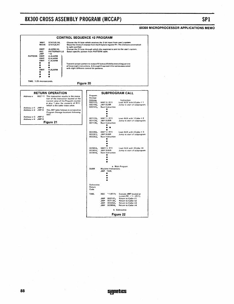
8X300 CROSS ASSEMBLY PROGRAM (MCCAP) SPI 8X300 MICROPROCESSOR APPLICATIONS MEMO
XMIT MOVE
XMIT XEC JMP
PATTERN XMIT XMIT XMIT
• • • XMIT
• • ~
CONTROL SEQUENCE #2 PROGRAM STATUS,IVl STATUS,R1
ALARM,IVL PATTERN(R1),8 *+9 A,ALARM B,ALARM C,ALARM
• • • H,ALARM
• • •
Choose the IV byte which receives the 3·bit input from user's system. Move the 3 bits of interest from the IV byte to register R 1 . The 3 bits are automatical· IV right justified. Choose the IV byte through which the response is sent to the user's system. Select specific pattern from PATTERN table.
Transmit proper pattern to output IV byte subfield bV executing just one of these eight instructions. A through H represent the names associated with eight different control bit patterns.
TIME: 1.25 microseconds. Figure 20
RETURN OPERATION Address n XEC'+1 This instruction results in the execu·
Address n+1 JMP A
tion of the instruction located at the current value of the Program counter p plus 1 plus the contents of R 11, which is the caller index value.
Address n+2 JMP B The JMP table follows in consecutive Program Storage locations following SEC.
Address n+3 JMP C Address n+4 JMP 0
Figure 21
Program Storage Address 000137, 000140, 000141,
001133, 001134, 001135,
003260. 003261. 003262.
003654. 003655, 003656,
SUBPROGRAM CALL
XM1T0,R11 JMP SU8R Next Instruction
• • • • XM1T1,R11 JMP SUBR Next Instruction
• • • • XMIT 2, R11 JMP SU8R Next Instruction
• • • • XMIT 3, R11 JMP SUBR Next Instruction
• • • •
Instruction LoadAUX~ith o Caller ~ 1 Jump to start of subprogram.
load AUX with 1 Caller ~ 2 Jump to start of subprogram.
load AUX with 2Caller ~ 3· Jump to start of subprogram
load AUX with 3Caller #4 Jump to start of subprogram
a. Main Program SUBR Machine Instructions
88
Subroutine Return Code
TABl
JMP TABl
• • • •
XEC *+1(R11)
JMP 000141. JMP 001135. JMP 003262. JMP 003656.
Execute JMP located at currentPC + 1 + (R11). Return to Caller 111 Return to Caller 112 Return to Caller 113 Return to Caller 114
b. Subroutine
Figure 22
Si!lDOliC!i
8X300 PROGRAM LIBRARY
INTRODUCTION The MicroControlier Program Library is made up of commonly required subprograms in the form of procedures and the documentation for each of these procedures. The Library is intended to support applications for the MicroControlier. These applications may be written in the MicroController Cross Assembler (MCCAP) language, a stand-alone ANSI FORTRAN assembler intended to execute on any 16-bit or larger minicomputer.
SPECIAL RESTRICTIONS WHEN USING THE CROSS ASSEMBLER Where IV Bytes and Working Storage allocations are required by a procedure, they have been made. These arbitrary definitions should be reviewed by the procedure user
and modified as necessary to fit his application. There are two characteristics of the library procedures that require special attention by the user. First of all, procedures from the library may in turn call on other library procedures. For example, a procedure which generates square roots would make calls on a division and possibly a multiplication procedure. These calls, if any, are noted in the documentation for each procedure. The programmer must be aware of these calls because he must append these secondary procedures to his program.
The second characteristic is that the Cross Assembler has two instructions (XEC, NZT) whose operands are required to be within the same register page and/or memory page. It is difficult, if not impossible, to
!ijgDOliCS
83
determine before compile time whether or not these ranges will be exceeded. The solution is to code conditional ORG statements which, when properly used, align the program with the next page boundary only when necessary. Conditional ORG statements have been included in all the library procedures. These statements should prevent most, but not necessarily all, range errors within the procedure. The customer may find it necessary to encode additional ORG statements in some instances. The user should be aware that this solution creates blocks of unused memory in program storage. The programmer should be aware of these blocks because it is usually possible to reorganize code to either eliminate them completely or at least keep their size to a minimum.
89
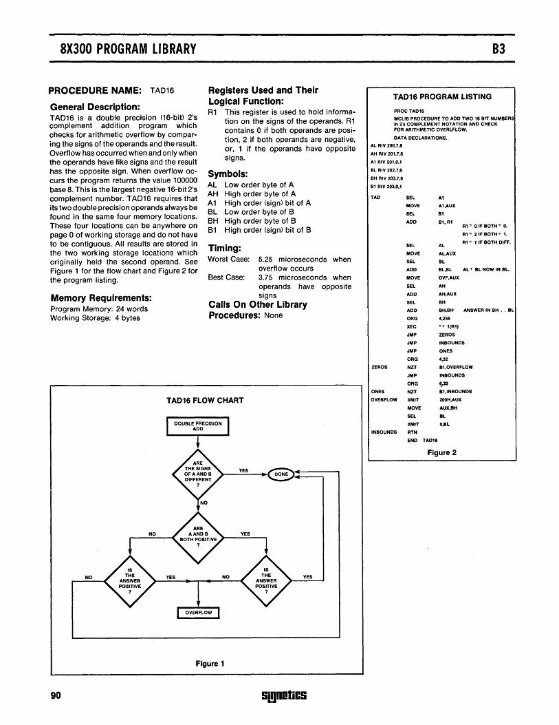
8X300 PROGRAM LIBRARY
PROCEDURE NAME: TAD16
General Description: TAD16 is a double precision (16-bit) 2's complement addition program which checks for arithmetic overflow by comparing the signs of the operands and the result. Overflow has occurred when and only when the operands have like signs and the result has the opposite sign. When overflow occurs the program returns the value 100000 base 8. This is the largest negative 16-bit 2's complement number. TAD16 requires that its two double precision operands always be found in the same four memory locations. These four locations can be anywhere on page 0 of working storage and do not have to be contiguous. All results are stored in the two working storage locations which originally held the second operand. See Figure 1 for the flow chart and Figure 2 for the program listing.
Memory Requirements: Program Memory: 24 words Working Storage: 4 bytes
Registers Used and Their Logical Function: R1 This register is used to hold informa
tion on the signs of the operands. R1 contains 0 if both operands are position, 2 if both operands are negative, or, 1 if the operands have opposite signs.
Symbols: AL Low order byte of A AH High order byte of A A1 High order (sign) bit of A BL Low order byte of B BH High order byte of B B1 High order (sign) bit of B
Timing: Worst Case: 5.25 microseconds when
overflow occurs Best Case: 3.75 microseconds when
operands have opposite signs
Calls On Other Library Procedures: None
TAD16 FLOW CHART
YES ~ >-------~4-----.
NO YES NO YES
Figure 1
90 SmnOliCS
B3
TAD16 PROGRAM LISTING
PROCTAD16
MCLlB PROCEDURE TO ADD TWO 16 BIT NUMBERS in 2'5 COMPLEMENT NOTATION AND CHECK FOR ARITHMETIC OVERLFLOW.
DATA DECLARATIONS.
AL RIV 200,7,8
AH RIV 201,7,8
A1 RIV 201,0,1
BL RIV 202,7,6
BH RIV 203,7,8
B1 RIV 203,0,1
TAD
ZEROS
ONES
OVERFLOW
SEL A1
MOVE A1,AUX
SEL 81
ADD B1.R1 RF: 0 IF 80TH = O.
R1= 21F80TH= 1.
R1 = 1 IF 80TH DIFF. SEL
MOVE
SEL
ADD
MOVE
SEL
ADD
SEL
ADD
ORG
XEC
JMP
JMP
JMP
ORG
NZT
JMP
ORG
NZT
XMIT
MOVE
SEL
AL
Al,AUX
8L
8L.BL AL + 8L NOW IN BL.
OVF.AUX
AH
AH.AUX
8H
BH.BH ANSWER IN BH , • BL
4.256
.+ 1(R1)
ZEROS
IN80UNDS
ONES
4.32
81.0VERFLOW
INBOUNDS
~32
B1.INBOUNDS
2OOH.AUX
AUX.BH
BL
XMIT 0.8L
IN80UNDS RTN
END TAD16
Figure 2
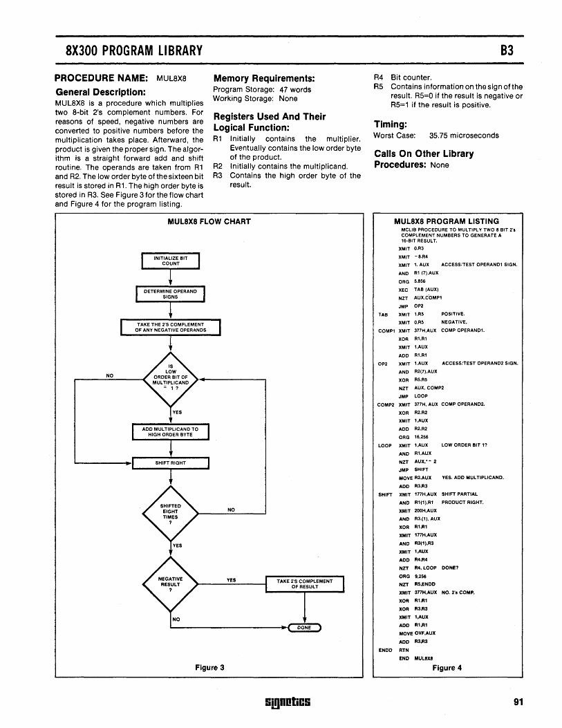
8X300 PROGRAM LIBRARY
PROCEDURE NAME: MUL8X8
General Description: MUL8X8 is a procedure which multiplies two 8-bit 2's complement numbers. For reasons of speed, negative numbers are converted to positive numbers before the multiplication takes place. Afterward, the product is given the proper- sign. The algorithm is a straight forward add and shift routine. The operands are taken from R1 and R2. The low order byte of the sixteen bit result is stored in R1. The high order byte is stored in R3. See Figure 3 for the flow chart and Figure 4 for the program listing.
Memory Requirements: Program Storage: 47 words Working Storage: None
Registers Used And Their Logical Function: R1
R2 R3
Initially contains the multiplier. Eventually contains the low order byte of the product. Initially contains the multiplicand. Contains the high order byte of the result.
MUL8X8 FLOW CHART
NO
NO
YES TAKE 2'S COMPLEMENT OF RESULT
L-________________________ .( DONE)
Figure 3
S!!IDOliCS
B3
R4 Bit counter. R5 Contains information on the sign of the
result. R5=O if the result is negative or R5=1 if the result is positive.
Timing: Worst Case: 35.75 microseconds
Calls On Other Library Procedures: None
MUL8X8 PROGRAM LISTING
TAB
COMPl
MCLlB PROCEDURE TO MUL TIPL Y TWO 8 BIT 2'5 COMPLEMENT NUMBERS TO GENERATE A 1S-BIT RESULT.
XMIT O.R3
XMIT -8.R4
XMIT 1. AUX ACCESS/TEST OPERAND1 SIGN.
AND R1 (7).AUX
ORG 5.856
XEC TAB (AU X)
NZT AUX.COMP1
JMP OP2
XMIT 1.R5 POSITIVE.
XMIT O.R5 NEGATIVE.
XMIT 377H.AUX COMP OPERAND1.
XOR Rl.Rl
XMIT 1.AUX
ADO Rl.R1
OP2 XMIT 1.AUX ACCESSITEST OPERAND2 SIGN.
AND R2(7).AUX
XOR R5.R5
NZT AUX. COMP2
JMP LOOP
COMP2 XMIT 377H. AUX COMP OPERAND2.
XOR R2.R2
XMIT 1.AUX
ADO R2.R2
ORG 16.256
LOOP XMIT 1.AUX
AND R1.AUX
LOW ORDER BIT 11
SHIFT
ENDD
NZT AUX:+ 2
JMP SHIFT
MOVE R2.AUX YES. ADO MULTIPLICAND.
ADD R3.R3
XMIT 177H.AUX SHIFT PARTIAL
AND R1(1).R1 PRODUCT RIGHT.
XMIT 200H.AUX
AND R3.(1). AUX
XOR Rl,Rl
XMIT l77H.AUX
AND R3(1),R3
XMIT 1,AUX
ADD R4.R4
NZT R4, LOOP DONE?
ORG 9,256
NZT R5,ENDD
XMIT 377H,AUX NO.2', COMPo
XOR Rl,Rl
XOR R3,R3
XMIT 1.AUX
ADD Rl.R1
MOVE OVF,AUX
ADD R3.R3
RTN
END MUL8xa
Figure 4
91
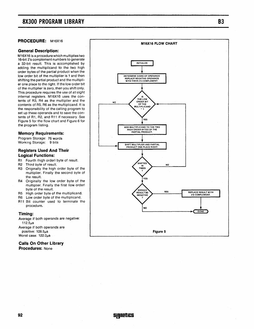
8X300 PROGRAM LIBRARY
PROCEDURE: M16X16
General Description: M16X16 is a procedure which multiplies two 16-bit 2's complement numbers to generate a 32-bit result. This is accomplished by adding the multiplicand to the two high order bytes of the partial product when the low order bit of the multiplier is 1 and then shifting the partial product and the multiplier one place to the right. If the low order bit of the multiplier is zero, then you shift only. This procedure requires the use of all eight internal registers. M16X16 uses the contents of R3, R4 as the multiplier and the contents of RS, R6 as the multiplicand. It is the responsibility of the calling program to set up these operands and to save the contents of R1, R2, and R11 if necessary. See Figure S for the flow chart and Figure 6 for the program listing.
Memory Requirements: Program Storage: 76 words Working Storage: 9 bits
Registers Used And Their Logical Functions: R1 Fourth (high order) byte of result. R2 Third byte of result. R3 Originally the high order byte of the
multiplier. Finally the second byte of the result.
R4 Originally the low order byte of the multiplier. Finally the first (low order) byte of the result.
RS High order byte of the multiplicand. R6 Low order byte of the multiplicand. R11 Bit counter used to terminate the
procedure.
Timing: Average if both operands are negative:
112.S~s
Average if both operands are positive: 1 09.S~s
Worst case: 122.0J,Ls
Calls On Other Library Procedures: None
92
NO
M16X16 FLOW CHART
DETERMINE SIGNS OF OPERANDS REPLACE NEGATIVE OPERANDS WITH THEIR 2'S COMPLEMENT.
ADD MULTIPLICAND TO THE TWO HIGH ORDER BYTES OF THE
PARTIAL PRODUCT.
SHIFT MULTIPLIER AND PARTIAL PRODUCT ONE PLACE RIGHT.
NO
YES REPLACE RESULT WITH 2'S COMPLEMENT.
~--------------------~I( DONE)
Figure 5
lii!)DOliCS
B3
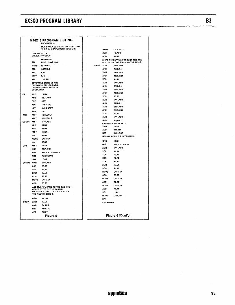
8X300 PROGRAM LIBRARY B3
M16X16 PROGRAM LISTING PROC M16X16
MCLIB PROCEDURE TO MULlTPL Y TWO 16-BIT' 2's COMPLEMENT NUMBERS. MOVE OVF. AUX
LINK RIV 200,7,8 ADD R5,AUX
SRESULT PIV 201,7,1 ADD Rl,Rl
INITIALIZE SHIFT THE PARTIAL PRODUCT AND THE SEL LINK SAVE LINK. MULTIPLIER ONE PLACE TO THE RIGHT.
MOVE Rll,LINK SHIFT XMIT l77H,AUX
SEL SRESULT AND R4(1),R4
XMIT O,Rl XMIT 200H,AUX
XMIT O,R2 AND R3(1),AUX
XMIT -16,R1l XOR R4,R4
DETERMINE SIGNS OF THE XMIT 177H,AUX OPERANDS. REPLACE NEG. AND R3(1),R3 OPERANDS WITH THEIR 2'5 COMPLEMENT. XMIT 200H,AUX
OPl XMIT l,AUX AND R2(1),AUX
AND R3(7),AUX XOR R3,R3
ORG 6,256 XMIT 177H,AUX
XEC TAB(AUX) AND R2(1),R2
NZT AUX,COMPl XMIT 200H,AUX
JMP OP2 AND Rl(l),AUX
TAB XMIT l,SRESULT XOR R2,R2
XMIT O,SRESULT XMIT 177H,AUX
COMPl XMIT 377H,AUX AND Rl(l),Rl
XOR R4,R4 SHIFTED 16 TIMES VET?
XMIT l,AUX XOR R3,R3
ADD Rll,Rll XMIT l,AUX
NZT Rll,LOOP ADD R4,R4 NEGATE RESULT IF NECESSARY. MOVE OVF,AUX
ADD R3,R3 ORG 14,32
OP2 XMIT l,AUX NZT SRESUL T,ENDD
AND R5(7),AUX XMIT 377H,AUX
XOR SRESUL T,SRESULT XOR R4,R4
NZT AUX,COMP2 XOR R3,R3
JMP LOOP XOR R2,R2
COMP2 XMIT 377H,AUX XOR Rl,Rl
XOR RS,R6 XMIT 1,AUX
XOR RS,R5 ADD R4,R4
XMIT 1,AUX MOVE OVF,AUX
ADD R6,RS ADD R3,R3
MOVE OVF,AUX MOVE OVF,AUX
ADD RS,RS ADO R2,R2
ADD MULTIPLICAND TO THE TWO HIGH MOVE OVF,AUX
ORDER BYTES OF THE PARTIAL ADD Rl,Rl PRODUCT IF THE LOW ORDER BIT OF SEL LINK THE MULTIPLIER IS 1.
MOVE LINK,Rll
ORG 29,256 RTN
LOOP XMIT 1,AUX END M1SX16
AND R4,AUX
NZT AUX .... 2
JMP SHIFT
Figure 6 Figure 6 (Cont'd)
!ii!)DotiC!i 93
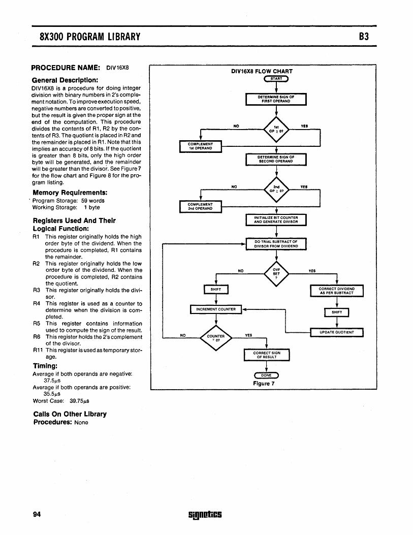
8X300 PROGRAM LIBRARY
PROCEDURE NAME: DIV16X8
General Description: DIV16X8 is a procedure for doing integer division with binary numbers in 2's comple· ment notation. To improve execution speed, negative numbers are converted to positive, but the result is given the proper sign at the end of the computation. This procedure divides the contents of A1, A2 by the contents of A3. The quotient is placed in A2 and the remainder is placed in A1. Note that this implies an accuracy of 8 bits. If the quotient is greater than 8 bits, only the high order byte will be generated. and the remainder will be greater than the divisor. See Figure 7 for the flow chart and Figure 8 for the program listing.
Memory Requirements: . Program Storage: 59 words
Working Storage: 1 byte
Registers Used And Their Logical Function: R1 This register originally holds the high
order byte of the dividend. When the procedure is completed. A1 contains the remainder.
R2 This register originally holds the low order byte of the dividend. When the procedure is completed. A2 contains the quotient.
R3 This register originally holds the divisor.
R4 This register is used as a counter to determine when the division is completed.
A5 This register contains information used to compute the sign of the result.
R6 This register holds the 2's complement of the divisor.
R11 This register is used as temporary storage.
Timing: Average if both operands are negative:
37.511S
Average if both operands are positive: 35.5115
Worst Case: 39.75115
Calls On Other Library Procedures: None
94
B3
DIV16X8 FLOW CHART
NO
NO
NO
NO
Figure 7
9i!1DDliC9
8X300 PROGRAM LIBRARY B3
DIV16X8 PROGRAM LISTING
PROC DIV111X8
111-BIT BY 11-8IT 2's COMP DIVIDE WITH DIVIDEND IN Rl,R2 AND DIVISOR IN R3
LINK RIV 200,7,8
SEL LlNI{ SAVE LINK.
MOVE Rll,LINK
OP1 XMIT 1,AUX ACCESS/TEST OPll SIGN
AND Rl(7),AUX
XEC TA8(AUX)
NZT AUX,COMP1
JMP OP2
TAe XMIT 1,Rs POSITIVE
XMIT O,Pls
COMPl XMIT 377H,AUX 2'. COMP DIVIDEND
XOR Pll.Rl
XOR R2.R2
XMIT 1,AUX
ADD Pl2.Ft2
MOVE OVF.AUX
ADD Pll,Ftl
OP2 XMIT 1,AUX
AND Pl3(7),AUX ACCESSITEST DIVISOR SIGN
XOPI 1'15.1'15
NZT AUX,COMP2
JMP STAAT
COMP2 XMIT 377H.AUX
XOR 1'13,1'13 2's COMPLEMENT DIVISOPI
XMIT l,AUX
ADD R3,R3
START XMIT -!l,R4
XMIT 377H,AUX NEGATIVE OF DIVISOR
XOR 1'13,FIIS
XMIT l,AUX
ADD PlII,RII
OI'lG 20,258
LOOP MOVE I'II1,AUX
ADD I'll ,Pill TRIAL SUeTRACT
ORG 11,258
NZT OVF,DIVt DIVa MOVE R2,AUX SHIFT LEFT f
ADD R2,Pl2
MOVE OVF,AUX
ADD Rl,AUX
ADD Rl,Rl
JMP CHECK
DIVl MOVE R",R1 UPDATE DIVIDEND
MOVE R2,AUX
ADD R2,R2
MOVE OVF,AUX
ADD I'Il,AUX
ADD Rl,Rl
XMIT l,AUX SHIFT ON ..
XOR R2,I'I2
NZT R4,LOOP DONE?
ORG 9,2511
NZT RS,ENDD YES. TEST SIGN RESULT
XMIT 377H,AUX
XOR Rl,Rl
XOR R2,R2
XMIT 1.AUX
ADD Rl.Rl
MOVE OVF,AUX
ADD R2,Fl2
ENDD SEL LINK I'IESTORE RETURN LINK.
MOVE LINK,A"
IITN
END DIV18X8
Figure 8
9!!1DOliC9 95
8X300 PROGRAM LIBRARY
PROCEDURE NAME: D24X12
General Description: D24X12 is a procedure to do integer division with 2's complement numbers. To improve execution speed, any negative operands are first converted to positive. However, the quotient is given the proper sign at the end of the computation. D24X12 divides the contents of R1, R2, R3 by the 410w order bits of RS and R4. The quotient is stored in the 4 low order bits of R2 and R3. The remainder is stored in R1 and the 4 high order bits of R2. Note this implies a 12-bit result. If the quotient is greater than 12 bits only the 12 most significant bits will be generated, and the remainder may be larger than the divisor. Also note that if the divisor supplied by the main program is zero, then the dividend is merely rotated 12 places. See Figure 9 for the flow chart and Figure 10 forthe program listing.
Memory Requirements: Program Storage: 94 words Working Storage: 2 bytes
Registers Used And Their Logical Function: R1 This register originally contains the
high order byte of the dividend. At the end of the procedure, it contains the 8 high order bits of the remainder.
R2 This register originally contains the middle byte of the dividend. At the end of the procedure, it contains the 4 low order bits of the remainder and the 4 high order bits of the quotient.
R3 This register originally contains the low order byte of the dividend. At the end of the procedure, it contains the 8 low order bits of the quotient.
R4 This register originally contains the 4 high order bits of the divisor. Shortly after the procedure begins execution, R4 contains the 8 high order bits of the divisor.
RS This register originally contains the 8 low order bits of the divisor. Shortly after the procedure begins execution, RS contains the 4 low order bits of the divisor left justified.
R6 This register contains the high order 8 bits of the negated divisor.
R11 This register contains the 4 low order bits of the negated divisor. These bits are left justified.
Timing: Worst Case: 109,SJLS
Calls On Other Library Procedures: None
96
COMPLEMENT THE DIVIDEND
COMPLEMENT THE DIVISOR
YES
YES
sagDOliCS
83
D24X12 FLOW CHART
Figure 9
8X300 PROGRAM LIBRARY B3
D24X12 PROGRAM LISTING ADD R2,R2
PROC D24X12 MOVE OVF,AUX
MCLlB PROCEDURE TO DIVIDE A 24·BIT 2'5 ADD R1,R1 COMPLEMENT NUMBER. BY A 16·BIT 2's
MOVE R6,AUX COMPLEMENT NUMBER.
LINK RIV 200,7,8 ADD R1,R1
TEMP RIV 201,7,8 MOVE OVF,SWITCH TEMPH RIV 201,3,4
NZT OVF,DIV1 SIGN RIV 201,7,1 COUNT RIV 201,6,5 DIVO MOVE R5,AUX RESTORE ADD. SWITCH RIV 201,0,1
ADD R2,R2 SEL LINK
MOVE OVF,AUX MOVE R11,LINK SAVE RETURN LINK.
ADD R1,R1 BEGIN XMIT 360H,AUX ALIGN DIVISOR BY
MOVE R4,AUX SEL TEMP SHIFTING LEFT FOUR
ADD R1,R1 MOVE R5,TEMP PLACES.
DIV1 MOVE R3,AUX SHIFT LEFT 1 PLACE. AND R5(4),R5
ADD R3,R3 AND R4(4),AUX
MOVE OVF,AUX ADD TEMPH,R4
ADD R2,R2 XMIT -13,COUNT
MOVE OVF,AUX OP1 XMIT 1,AUX
ADD R1,R1 AND R1(7),AUX
MOVE R2,AUX XEC TAB(AUX)
ADD R2,R2 NZT AUX,COMP1
MOVE OVF,AUX JMP OP2
ADD R1,R1 TAB XMIT 1,SIGN
MOVE R1,AUX XMIT O,SIGN
ADD R1,R1 COMP1 XMIT 377H,AUX
XMIT 1,AUX XOR R3,R3
NZT SWITCH,*+2 XOR R2,R2
JMP CHECK XOR R1,R1
XOR R3,R3 BUILD UP QUOTIENT. XMIT 1,~X
CHECK ADD COUNT,COUNT ADD R3,R3
NZT COUNT,LOOP MOVE OVF,AUX
ORG 15,32 ADD R2,R2
NZT SIGN,ENDD MOVE OVF,AUX
XMIT 377H,AUX GIVE RESULT THE ADD R1,R1
XOR R1,R1 PROPER SIGN. XMIT 1,AUX
XOR R2,R2 OP2 AND R4(7),AUX
XOR R3,R3 XOR SIGN,SIGN
XMIT 20H,AUX NZT AUX,COMP2
ADD R2,R2 JMP START
MOVE OVF,AUX COMP2 XMIT 377H,AUX
ADD R1,R1 XOR R4,R4
MOVE OVF,AUX XMIT 360H,AUJ(
ADD R3,R3 XOR R5,R5
MOVE OVF,AUX XMIT 20H,AUX
ADD R2,R2 ADD R5,R5
ENDD SEL LINK RESTORE RETURN LINK. MOVE OVF,AUX
MOVE L1NK,R11 ADD R4,R4
RTN START XMIT 377H,AUX NEGATE DIVISOR.
END D24X12 XOR R4,R6
XMIT 360H,AUX Figure 10 (Cont'd) XOR R5,R11
XMIT 20H,AUX
ADD R11,R11
MOVE OVF,AUX
ADD R6,R6
ORG 32
Figure 10
!ii!)DotiCS 97
8X300 PROGRAM LIBRARY
PROCEDURE NAME: DTOB
General Description: DTOB is a procedure which converts 7 unsigned BCD digits, stored in consecutive Working Storage locations, into upto 24 bits of binary which is stored in R2, R3, R4. The main program must supply in R6 the byte address of the first (low order) BCD digit. DTOB expects to find this first digit right justified in the Working Storage byte. The first 6 BCD digits should be packed 2 per byte in ascending memory locations. The seventh BCD digit should be right justified in the last memory location. DTOB accomplishes the conversion by adding the proper power of 10 the proper number of times to R2, R3, R4. Finally, since most applications where BCD to binary conversion is neces· sary are not expected to require high speed, DTOB had traded off some speed in order to limit program storage requirements. See Figure 11 for the flow chart and Figure 12 for the program listing.
Memory Requirements: Program Storage: 56 words Working Storage: 41/2 bytes
Registers Used And Their Logical Functions: R1 This is a program control register used
to step through Working Storage and to properly access either the high or tow order four bits of an enabled Working Storage location.
R2 This register contains the high 8 bits of the binary result.
R3 This register contains the middle 8 bits of the binary result.
R4 This register contains the low 8 bits of the binary result.
R5 This register is loaded with the current BCD digit and isthen used asacounter to add a power of 10the proper number of times.
R6 This register is used to step through Working Storage. It originally contains the address of the first BCD digit to be converted, which is supplied by the main program.
R11 The contents of this register are used to select the proper power of 10 to be added to the partial binary sum. It is also used to terminate the procedure.
Timing: Worst Case: 222.75J.Ls (conversion of
9,999,999 to binary) Average Case: 132.75J.Ls (conversion of
5,555,555 to binary)
Calls On Other Library Procedures: None
98
83
DTOB FLOW CHART
>-----1.-'( DONE)
YES
YES
Figure 11
9!!1DOliC9
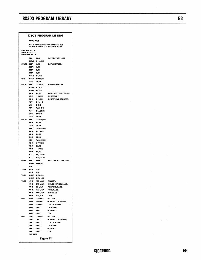
8X300 PROGRAM LIBRARY 83
OTOB PROGRAM LISTING
PROC DT08
MCLl8 PROCEDURE TO CONVERT 7 BCD DIGITS INTO UPTO 24 BITS OF BINARY.
LINK RIV 200,7,6 DMYL RIV 200,7,4 DMYH RIV 200,3,4
SEL LINK SAVE RETURN LINK.
MOVE R11,LlNK
START XMIT 0,1'13 INITIALIZATION.
XMIT 0,1'12
XMIT 0,1'11
XMIT 7,1'111
MOVE R6,IVR
ONE MOVE DMYL,R4
ORG 25,256
LOOP1 XEC TABA(R1) COMPLEMENT 1'11.
MOVE R1,AUX
MOVE R6,IVR
ADD R6,R6 INCREMENT ONLY WHEN
XMIT -1,AUX NECESSARY.
ADD 1'111,1'111 DECREMENT COUNTER.
NZT 1'111,*+2
JMP DONE
XEC TAB1(Pl1)
NZT RS,LOOP2
JMP LOOP1
ORG 25,256
LOOP2 XEC TAB3-1(R11)
ADD 1'14,1'14
ORG 29,256
XEC TAB4-1(1'I11)
ADD OVF,AUX
ADD 1'13,1'13
ORG 32,256
XEC TABS-1(1'I11)
ADD OVF,AUX
ADD 1'12,1'12
XMIT -1,AUX
ADD 1'15,1'15
NZT I'IS,LOOP2
NZT R11,LOOP1
DONE SEL LINK RESTORE RETURN LINK.
MOVE LINK,R11
RTN
TA8A XMIT 1,1'11
XMIT 0,1'11
TA81 MOVE DMYL,RS
MOVE DMYH,RS
TA83 XMIT 10OH,AUX MILLION.
XMIT 24OH,AUX HUNDRED THOUSAND.
XMIT 2OH,AUX TEN THOUSAND,
XMIT 35OH,AUX THOUSAND,
XMIT 144H,AUX HUNDRED
XMIT 12H,AUX TEN.
TA84 XMIT 102H,AUX MILLION.
XMIT 206H,AUX HUNDRED THOUSAND.
XMIT 47H,AUX TEN THOUSAND.
XMIT 3,AUX THOUSAND.
XMIT O,AUX HUNDRED,
XMIT O,AUX TEN.
TA8S XMIT 17H,AUX MILLION.
XMIT 1,AUX HUNDRED THOUSAND.
XMIT O,AUX TEN THOUSAND.
XMIT O,AUX THOUSAND.
XMIT O,AUX HUNDRED.
XMIT O,AUX TEN,
ENDDTOB
Figure 12
SmOOliCS 99
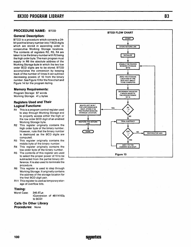
8X300 PROGRAM LIBRARY
PROCEDURE NAME: BTOD
General Description: BTOD is a procedure which converts a 24· bit positive binary number into 7 BCD digits which are stored in ascending order in consecutive Working Storage locations. The contents of registers R2, R3, R4 are taken to be the binary numberwith R2 being the high order byte. The main program must supply in R6 the absolute address of the Working Storage byte in which the two low order BCD digits are to be stored. BTOD accomplishes the conversion by keeping track of the number of times it can subtract decreasing powers of 10 from the binary number. See Figure 13 for the flow chart and Figure 14 for the program listing.
Memory Requirements: Program Storage: '87 words Working Storage: 41/2 bytes
Registers Used and Their Logical Functions: R1 This is a program control register used
to step through Working Storage and to properly access either the high or the low order BCD digit of an enabled Working Storage byte.
R2 This register originally contains the high order byte of the binary number. However, note that the binary number is destroyed as the BCD digits are computed.
R3 This register originally contains the middle byte of the binary number.
R4 This register originally contains the low order byte of the binary number.
R5 The contents of this register are used to select the proper power of 10 to be subtracted from the partial binary difference. It is also used to terminate the procedure.
R6 This register is used to step through Working Storage. It originally contains the address of the storage location for the first BCD digit pair.
R11 This register is used as temporary storage of overflow bits.
Timing: Worst Case: 346 .. 67IJ.s
(Conversion of 461141638 to BCD)
Calls On Other Library Procedures: None
WHATS LEFT IN R4= THE LOW ORDER BCD
DIGIT. STORE IT IN THE PROPER WORKING STORAGE LOCATION.
100 SJgDDliCS
BTOD FLOW CHART
ZERO THE STORAGE LOCATION OF THE BCD DIGIT ABOUT TO BE COMPUTED
DECREMENT REGISTER 5 WHICH SELECTS
THE PROPER POWER OF10
Figure 13
B3
RESTORATIVE ADD
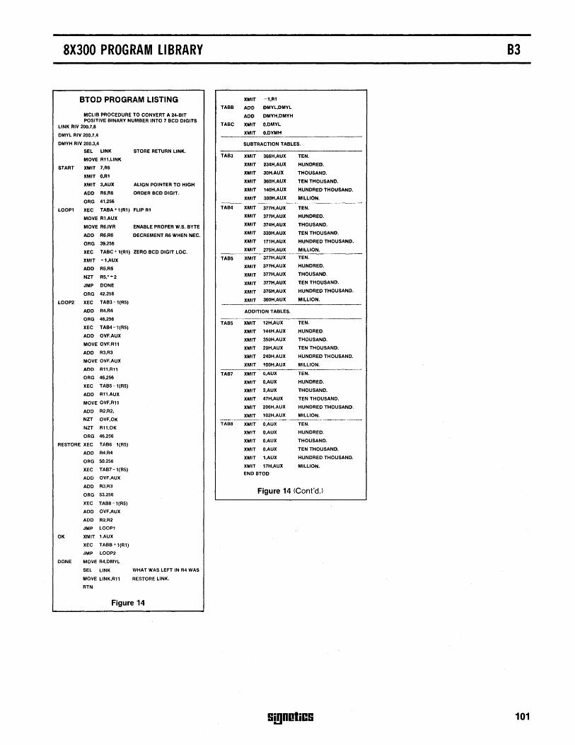
8X300 PROGRAM LIBRARY
BTOD PROGRAM LISTING
MCLIB PROCEDURE TO CONVERT A 24·BIT POSITIVE BINARY NUMBER INTO 7 BCD DIGITS
LINK RIV 200,7,8
DMYL RIV 200,7.4
DMYH RIV 200,3,4
SEL LINK
MOVE R11,LINK
START XMIT 7,RS
XMIT O,R1
XMIT 3,AUX
ADD R6,R6
ORG 41,256
LOOP1 XEC TABA+1(R1)
MOVE R1,AUX
MOVE R6,IVR
ADD R6,R6
ORG 39,256
XEC TABC+1(R1)
XMIT -l,AUX
ADD R5,R5
NZT R5:+2
JMP DONE
ORG 42,256
LOOP2 XEC TAB3-1(R5)
ADD R4,R4
ORG 46,256
XEC TAB4-1(R5)
ADD OVF,AUX
MOVE OVF,R11
ADD R3,R3
MOVE OVF,AUX
ADD R11,R11
ORG 46,256
XEC TAB5-1(R5)
ADD R11,AUX
MOVE OVF,R11
ADD R2,R2,
NZT OVF,OK
NZT R11,OK
ORG 46,256
RESTORE XEC TAB6-1(R5)
ADD R4,R4
ORG 50,256
XEC TAB7-1(R5)
ADD OVF,AUX
ADD R3,R3
ORG 53,256
XEC TAB8-1(R5)
ADD OVF,AUX
ADD R2,R2
JMP LOOP1
OK XMIT 1,AUX
XEC TABB+1(R1)
JMP LOOP2
DONE MOVE R4,DMYL
SEL LINK
MOVE L1NK,R11
RTN
STORE RETURN LINK.
ALIGN POINTER TO HIGH
ORDER BCD DIGIT.
FLIP R1
ENABLE PROPER W.S. BYTE
DECREMENT R6 WHEN NEC.
ZERO BCD DIGIT LOC.
WHAT WAS LEFT IN R4 WAS
RESTORE LINK.
Figure 14
B3
XMIT -l,R1
TABB ADD DMYL,DMYL
ADD DMYH,DMYH
TABC XMIT O,DMYL
XMIT O,DYMH
SUBTRACTION TABLES.
TAB3 XMIT 366H,AUX TEN.
XMIT 234H,AUX HUNDRED.
XMIT 30H,AUX THOUSAND.
XMIT 360H,AUX TEN THOUSAND.
XMIT 140H,AUX HUNDRED THOUSAND.
XMIT 300H,AUX MILLION.
TAB4 XMIT 377H,AUX TEN.
XMIT 377H,AUX HUNDRED.
XMIT 374H,AUX THOUSAND.
XMIT 330H,AUX TEN THOUSAND.
XMIT 171H,AUX HUNDRED THOUSAND.
XMIT 275H,AUX MILLION.
TABS XMIT 377H,AUX TEN.
XMIT 377H,AUX HUNDRED.
XMIT 377H,AUX THOUSAND.
XMIT 377H,AUX TEN THOUSAND.
XMIT 376H,AUX HUNDRED THOUSAND.
XMIT 360H,AUX MILLION.
ADDITION TABLES.
TABS XMIT 12H,AUX TEN.
XMIT 144H,AUX HUNDRED.
XMIT 350H,AUX THOUSAND.
XMIT 20H,AUX TEN THOUSAND.
XMIT 240H,AUX HUNDRED THOUSAND.
XMIT 100H,AUX MILLION.
TAB7 XMIT O,AUX TEN.
XMIT O,AUX HUNDRED.
XMIT 3,AUX THOUSAND.
XMIT 47H,AUX TEN THOUSAND.
XMIT 206H,AUX HUNDRED THOUSAND.
XMIT 102H,AUX MILLION.
TABS XMIT O,AUX TEN.
XMIT O,AUX HUNDRED.
XMIT O,AUX THOUSAND.
XMIT O,AUX TEN THOUSAND.
XMIT l,AUX HUNDRED THOUSAND.
XMIT 17H,AUX MILLION.
END BTOD
Figure 14 (Cont'd')
Si!lDotiC!i 101
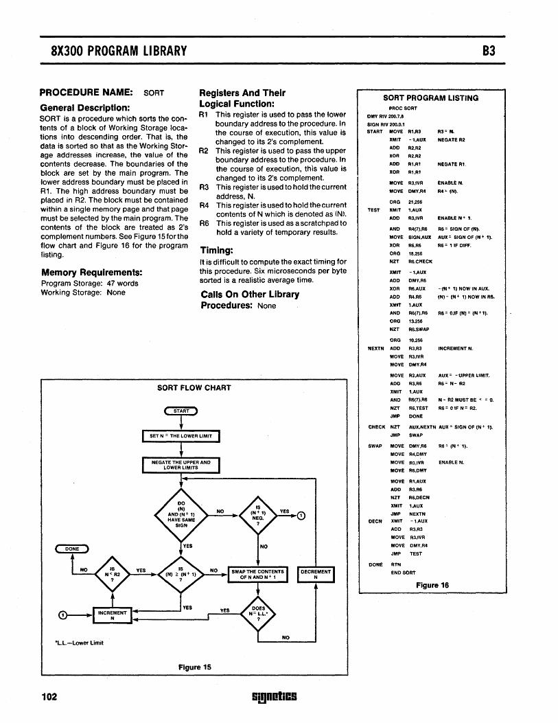
8X300 PROGRAM LIBRARY
PROCEDURE NAME: SORT
General Description: SORT is a procedure which sorts the con· tents of a block of Working Storage loca .. tions into descending order. That is. the data is sorted so that as the Working Stor· age addresses increase, the value of the contents decrease. The boundaries of the block are set by the main program. The lower address boundary must be placed in R1. The high address boundary must be placed in R2. The block must be contained within a single memory page and that page must be selected by the main program. The contents of the block are treated as 2's complement numbers. See Figure 15forthe flow chart and Figure 16 for the program Ilsting.
Memory Requirements: Program Storage: 47 words Working Storage: None
Registers And Their Logical Function: R1 This register is used to pass the 'ower
boundary address to the procedure. In the course of execution, this value is changed to its 2's complement
R2 This register is used to pass the upper boundary address to the procedure. In the course of execution, this value is changed to its 2's complement.
R3 This register is used to hold the current address, N.
R4 This register is used to hold the current contents of N which is denoted as (N).
R6 This register is used as a scratch pad to hold a variety of temporary results.
Timing: It is difficult to compute the exact timing for this procedure. Six microseconds per byte sorted is a realistic average time.
Calls On Other Library Procedures: None
SORT FLOW CHART
NO "Ll.--lower limit
Figure 15
102 Si!)DOliCS
83
SORT PROGRAM LISTING PROC SORT
OMV RIV 200.7.8
SIGN RIV 200.0.1
START MOVE R1.R3 R3= N.
XMIT -1.AUX NEGATE R2
ADD R2.R2
XOR R2.R2
ADD Rl.R1 NEGATE R1. XOR R1.R1
MOVE R3.IVR ENABLE N.
MOVE DMY.R4 R4" (N).
ORO 21.25S
TEST XMIT 1 .• AUX
ADD R3,lVR ENABLE N+ 1.
AND R4(7).RS RS = SIGN OF (N).
MOVE SIGN.AUX AUX = SIGN OF (N + 1).
XOR RS.RS RS = , IF DIFF.
ORG 18.25S
NZT RS.CHECK
XMtT -'.AUX
ADD DMY.R6
XOR R6,AUX -(N+ 'J NOW IN AUX.
ADD R4,R6 (N) - IN + 1) NOW IN R6.
XMIT 1.AUX
AND R6(7).,RS RS = O.IF IN) = (N + 1,.
ORG 13.25S
NZT R6.SWAP
ORG 10.256
NEXTN ADD R3.R3 INCREMENT N.
MOVE R3.IVR
MOVE DMY.R4
MOVE R2.AUX AUX = - UPPER LIMIT.
ADD R3.RS RS= N- R2
XMIT 1.AUX
AND RS(7),R6 N - R2 MUST BE < = o. NZT R6.TEST R6= OIF N= R2.
JMP DONE
CHECK NZT AUX.NEXTN AUX '" SIGN OF IN + I,. JMP SWAP
SWAP MOVE DMY.RS RS = (N+ 1).
MOVE R4.DMY
MOVE R3,IVR ENABLE N.
MOVE R6,DMT
MOVE Rl,AUX
ADD R3,R6
NZT R6.DECN
XMIT 1.AUX
JMP NEXTN
OECN XMIT -l,AUX
ADD R3.R3
MOVE R3.IVR
MOVE DMY.R4
JMP TEST
OONE RTN
END SORT
Figure 16
8X300 PROGRAM LIBRARY
PROCEDURE NAME: FPADD
General Description: FPADD performs a double precision floating point addition of two operands located anywhere in the same page of Working Storage. These floating point operands must have an 8-bit exponent and a 16-bit manti sa. If the exponent of an operand is found in memory location N, then the high order byte of the mantisa must be in location N + 1. The low order byte must be in location N + 2. Both the exponent and the mantisa must be represented in 2's complement notation. The calling program specifies the operands to be added by passing the addresses of their exponents in R1 and R2 and by selecting the proper memory page before calling FPADD. FPADD begins processing by comparing the relative sizes of the two exponents. Because the precision of the addition is 16 bits, if the exponents differ by more than 15, the answer will be equal to the larger of the two operands. If the addition is meaningful, FPADD computes the exponent of the result and then calls a procedure to adjust the smaller of the operands so that the exponents of the operands 'are equal. FPADD then calls another procedure which performs the actual 16-bit addition. See Figure 17 for the flow chart and Figure 18 for the program listing.
Memory Requirements: Program Storage: 38 words Working Storage: 1 byte
Registers Used And Their Logical Funtions: R1 This register contains the address of
the exponent of the first operand. This address must be supplied by the main program.
R2 This register contains the address of the exponent of the second operand. This address must be supplied by the main program. R2 is also used to return the address of the exponent of the answer to the main program.
R3 Initially this register is used to hold the value of the exponent of the first operant (X11. Later it is used to pass the add ress of the exponent of the operand which will be adjusted before the addition takes place.
RS This register is used as a scratchpad throughout most of the procedure, but is also used to pass the address of the high order byte of the first operand to the addition procedure.
R6 This register is used as a scratch pad, but also passes the number of places which the smaller of the two operands must be shifted. Finally, it is used to pass the address of the high order byte of the second operand to the addition procedure.
Timing: Worst Case
B3
(exponents differ but by less than 16, and the addition overflows) "" 22 microseconds. This is the time from when FPADD is called to when it returns.
R11 In programs written in MCCAP, this register is used to hold the return link for subroutines.
Calls On Other Library Procedures:
!i!DOliC9
DSHIFT TAD16F
FPADD FLOW CHART
Figure 17
103
8X300 PROGRAM LIBRARY
FPADD PROGRAM LISTING
PROC FPADD
MCLIB PROCEDURE TO ADD TWO FLOATING POINT DOUBLE PRECISION 2', COMPLEMENT NUMBERS.
LINK RIV 200,7,8 Xl RIV 200,7.8 X2 RIV 200,7,8
NOTE THAT Xl AND X2 ARE NEVER TRANSMITED TO THE IVR REG. THUS THE ADDRESSES ASIGNED TO THESE VARIABLES ARE NOT IMPORTANT.
SEL LINK SAVE FPADD RETURN LINK.
MOVE Rll.LINK
START MOVE Rl.IVR ENABLE Xl.
MOVE Xl,R3
MOVE R2,IVR ENABLE X2.
XMIT -t.AUX
ADD R3.RS TAKE 2'5 COMP OF Xl.
XOR RS,AUX -Xl IN AUX.
ADD X2,RS X2-XlIN RS.
NZT RS,'+Z
JMP ADDD EXPONENTS MATCH.
XMIT 1.AUX
AND RS(7),R4 RS= SIGN OF X2 -Xl,
NZT RS,NEG
POS XMIT -lS.AUX RS IS POS, MEANING X2 IS GREATER THAN Xl.
ADD RS.RS DO X2 AND Xl DIFFER BY MORE THAN 151
NZT OVF,DONE OP2 IS THE ANSWER.
MOVE Rl.R3 THE ADDITION IS POSSIBLE BUT
JMP ADJ OPl MUST BE SHIFTED.
NEG XMIT -l,AUX RS IS NEG, MEANING Xl IS GREATER THAT X2.
ADD RS,RS MAKE RS POSITIVE.
XOR RS,RS
XMIT -lS,AUX DO Xl AND X2 DIFFER BY MORE THAN lS1
ADD RS.RS
NZT OVF,SWAP OPl IS THE ANSWER.
MOVE R3,X2
MOVE R2,R3
JMP ADJ
SWAP MOVE Rl,R2
JMP DONE
ADJ CALL DSHIFT
ADDD XMIT 1.AUX
ADD Rl,RS
ADD R2,RS
CALL TAD1SF
DONE SEL LINK
104
MOVE LINK,Rll
RTN
END FPADD
THE ANSWER WILL BE IN OP2 AND HAVE Xl AS AN EXPONENT. THE ADDITION IS POSSIBLE BUT
OP2 MUST BE SHIFTED.
WHEN THE PROC RETURNS,R2
MUST HOLD THE ADDRESS OF THE
RESULT.
R5 POINTS TO HOB OF OP1.
RS POINTS TO HOB OF OP2.
RESTORE FPADD RETURN LINK.
AT THIS POINT R2 POINTS TO
THE ANSWER.
Figure 18
B3
S!!)Dl!liCS
8X300 PROGRAM LIBRARY
PROCEDURE NAME: DSHIFT
General Description: DSHIFT is a program storage intensive high speed procedure which shifts a double precision variable on the right bank IV 1 to 15 bits to the right. The execution time is independent of the number of bits to be shifted and is fixed. Changing the 3 occurences of "IVR" in the procedure to "IVL" converts DSH I FT to operate on left bank IV variables. Ifthe high order byte of the double precision variable is in location N, then the low order byte must be in location N + 1. See Figure 19 for the flow chart and Figure 20 for the program listing.
Memory Requirements: Program Storage: 52 words Working Storage: None
Registers Used And Their Logical Functions: R3 This register is used to pass the ad
dress of the variable's high order byte to the procedure.
R4 This register is used to hold and rotate the variable's high order byte.
R5 This register is used to hold and rotate the variable's low order byte.
R6 This register is used to pass the number of places that the variable must be shifted to the procedure. If the con-
!imDDtiC!i
83
tents of R6 is outside the range of 1 to 15 errors will occur.
R11 In programs written for MCCAP, this register holds the procedure reJurn link.
Timing: 4.75 microseconds
Calls On Other Library Procedures: None
105
8X300 PROGRAM LIBRARY 83
DSHIFT PROGRAM LISTING TAB2 MOVE R4.Hl -,-
PROC DSHI" MOVE R4.H2
MCLlB PROCEDURE TO SHIFT A DOUBLE MOVE R4.H3
PRECISION VARIABLE IN WORKING STORAGE MOVE R4.HS
1 TO lS PLACES TO THE RIGHT, MOVE R4.H6
DMY RIV 201.7.8 MOVE R4.H7
Hl RIV 201.0.1 MOVE R4.DMY -.-
H2 RIV 201.1,2 TAB4 MOVE R4.L7
H3 RIV 201.2.3 MOVE R4.La
H4 RIV 201.3.4 MOVE R4.L5
HS RIV 201.4.S MOVE R4.L4
H6 RIV 201.S.6 MOVE R4.L3
H7 RIV 201.6.7 MOVE R4.L2
MOVE R4.Ll -I.- --L1 RIV 201.7.1 TABl MOVE R5(1).RS
L2 RIV 201.7.2 MOVE R5(2).RS L3 RIV 201.7.3 MOVE R5(3).RS L4 RIV 201.7.4 MOVE R5(4).RS LS RIV 201.7.5 MOVE RS(5).RS L6 RIV 201.7.6 MOVE RS(II).RS L7 RIV 201.7.7 MOVE R5(7).RS _ ....
-.-NOTE THAT NONE OF THE VARIABLES DECLARED IN THIS NOP PROCEDURE ARE EVER TRANSMITTED TO THE IVR REG.
TAB3 MOVE R4(1).R4 THUS IT IS NOT IMPORTANT WHAT ADDRESS THEY ARE ASIGNED TO. MOVE R4(2).R4
SHIFT XMIT 1.AUX MOVE R4(3).R4
ADD R3.IVR ENABLE HIGH ORDER BYTE. MOVE R4(4).R4
MOVE DMY.R4 MOVE R4(5).R4
XMIT O.DMY MOVE R4(6).R4
XMIT 2.AUX MOVE R4(7).R4 ..... 1.-
ADD R3.IVR ENABLE LOW ORDER BYTE. NOP
MOVE DMY.RS XMIT 0.H1
ORG 40.256 XMIT 0.H2
XEC TAB1-1(R6) XMIT 0.H3
MOVE RS.DMY XMIT 0.H4
XEC TAB2-1(RII) XMIT O.HS
ORG 45.2S6 XMIT 0.H6 -"-
XEC TAB3-1(R6) XMIT 0.H7
XMIT 1.AUX END DSHIFT
ADD R3.IVR ENABLE HIGH ORDER BYTE.
XEC TAI!I4-1(RS)
DONE RTN Figure 20 (Cont'dJ
Figure 20
106 SjgnOliCS
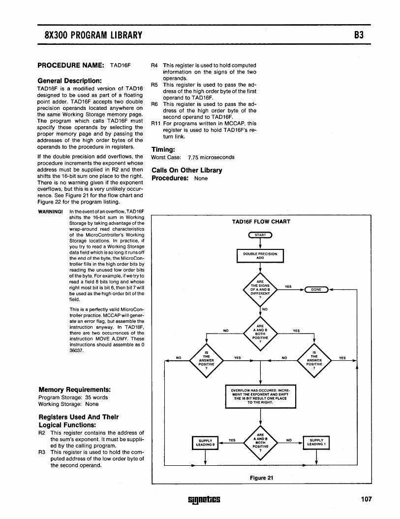
8X300 PROGRAM LIBRARY
PROCEDURE NAME: TAD16F
General Description: TAD16F is a modified version of TAD16 designed to be used as part of a floating pOint adder. TAD16F accepts two double precision operands located anywhere on the same Working Storage memory page. The program which calls TAD16F must specify these operands by selecting the proper memory page and by passing the addresses of the high order bytes of the operands to the procedure in registers.
If the double precision add overflows, the procedure increments the exponent whose address must be supplied in R2 and then shifts the 16-bit sum one place to the right. There is no warning given if the exponent overflows, but this is a very unlikely occurrence. See Figure 21 for the flow chart and Figure 22 for the program listing.
WARNINGI In the event of an overflow, TAD16F shifts the 16-bit sum in Working Storage by taking advantage of the wrap-around read characteristics of the MicroControlier's Working Storage locations. In practice, if you try to read a Working Storage data field which is so long it runs off the end of the byte, the MicroController fills in the high order bits by reading the unused low order bits of the byte. For example, if we try to read a field 8 bits long and whose right most bit is bit 6, then bit 7 will be used as the high order bit of the field.
This is a perfectly valid MicroController practice. MCCAP will generate an error flag, but assemble the instruction anyway. In TAD16F, there are two occurrences of the instruction MOVE A,DMY. These instructions should assemble as 0 36037.
Memory Requirements: Program Storage: 35 words Working Storage: None
Registers Used And Their Logical Functions: R2 This register contains the address of
the sum's exponent. It must be supplied by the calling program.
R3 This register is used to hold the computed address of the low order byte of the second operand.
R4 This register is used to hold computed information on the signs of the two operands.
R5 This register is used to pass the address of the high order byte of the first operand to TAD16F.
R6 This register is used to pass the address of the high order byte of the second operand to TAD16F.
R11 For programs written in MCCAP, this register is used to hold TAD16F's return link.
Timing: Worst Case: 7.75 microseconds
Calls On Other Library Procedures: None
TAD16F FLOW CHART
B3
>-__ YE_S __ ~( DONE )~ ______ ~
NO
NO
S!!)DDliCS
YES NO
OVERFLOW HAS OCCURED. INCRE· MENT THE EXPONENT AND SHIFT THE 16 81T RESULT ONE PLACE
TO THE RIGHT.
Figure 21
YES
107
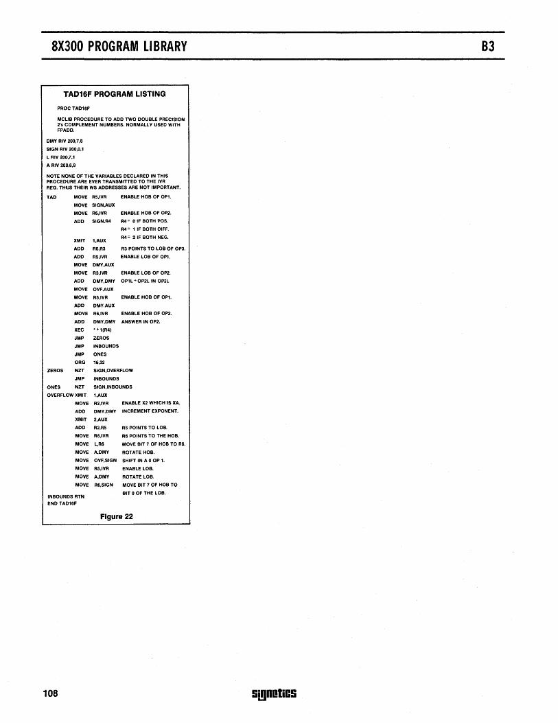
8X300 PROGRAM LIBRARY
TAD16F PROGRAM LISTING
PRoe TAD16F
MCLlB PROCEDURE TO ADD TWO DOUBLE PRECISION 2'5 COMPLEMENT NUMBERS. NORMALLY USED WITH FPADD.
DMY RIV 200,7,8
SIGN RIV 200,0,1
L RIV 200,7,1
A RIV 200,6,8
NOTE NONE OF THE VARIABLES DECLARED IN THIS PROCEDURE ARE EVER TRANSMITTED TO THE IVR REG. THUS THEIR WS ADDRESSES ARE NOT IMPORTANT.
TAD MOVE R5,IVR ENABLE HOB OF OP1.
MOVE SIGN,AUX
MOVE R6,IVR ENABLE HOB OF OP2.
ADD SIGN,R4 R4 = 0 IF BOTH POS.
R4 = 1 IF BOTH DIFF.
XMIT 1,AUX R4 = 2 IF BOTH NEG.
ADD R6,R3 R3 POINTS TO LOB OF OP3.
ADD R5,IVR ENABLE LOB OF OP1.
MOVE DMY,AUX
MOVE R3,IVR ENABLE LOB OF OP2.
ADD DMY,DMY OP1L + OP2L IN OP2L
MOVE OVF,AUX
MOVE R5,IVR ENABLE HOB OF OP1.
ADD DMY,AUX
MOVE R6,IVR ENABLE HOB OF OP2.
ADD DMY,DMY ANSWER IN OP2.
XEC *+1(R4)
JMP ZEROS
JMP INBOUNDS
JMP ONES
ORG 16,32
ZEROS NZT SIGN,OVERFLOW
JMP INBOUNDS
ONES NZT SIGN,INBOUNDS
OVERFLOW XMIT 1,AUX
MOVE R2,IVR ENABLE X2 WHICH IS XA.
ADD DMY,DMY INCREMENT EXPONENT.
XMIT 2,AUX
ADD R2,R5 R5 POINTS TO LOB.
MOVE R6,IVR R6 POINTS TO THE HOB.
MOVE L,R6 MOVE BIT 7 OF HOB TO R6.
MOVE A,DMY ROTATE HOB.
MOVE OVF,SIGN SHIFT IN A 0 OP 1.
MOVE R5,IVR ENABLE LOB.
MOVE A,DMY ROTATE LOB.
MOVE R6,SIGN MOVE BIT 7 OF HOB TO
IN BOUNDS RTN BIT 0 OF THE LOB.
END TAD16F
Figure 22
108
B3
SjgDOliCS

DATA SIIIITS
Si!lDOliCS 109

110 SmnOliCS
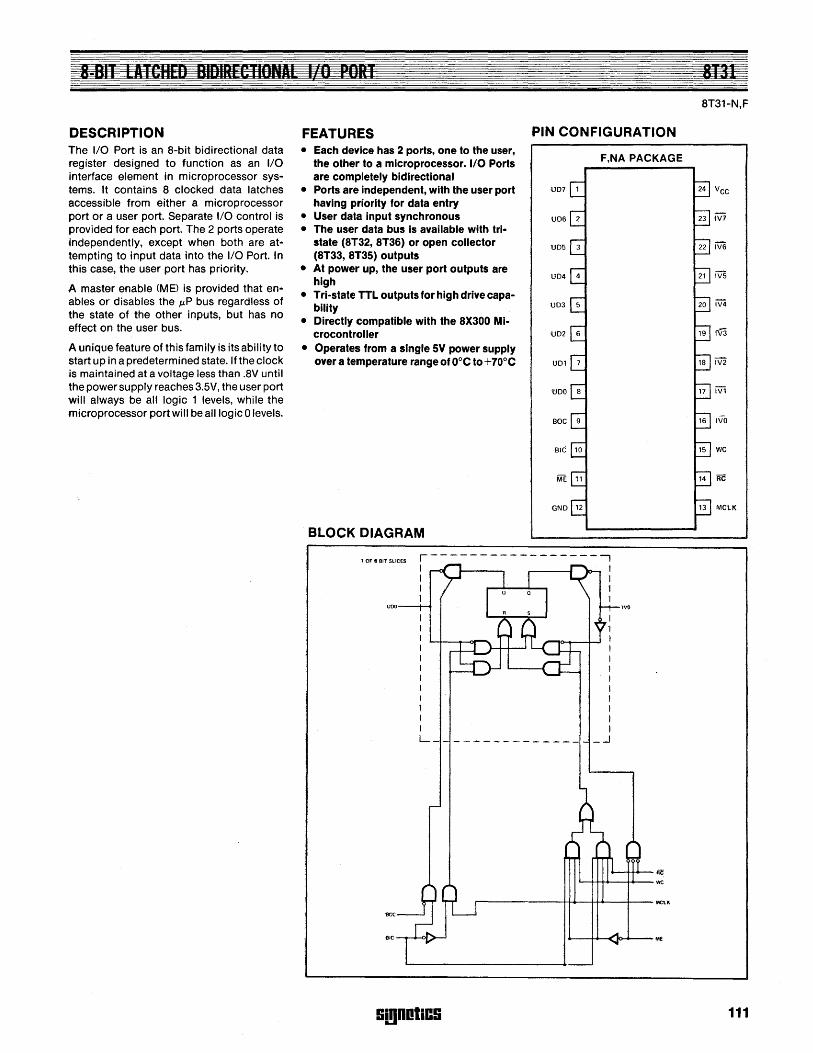
DESCRIPTION The I/O Port is an 8-bit bidirectional data register designed to function as an I/O interface element in microprocessor systems. It contains 8 clocked data latches accessible from either a microprocessor port or a user port. Separate I/O control is provided for each port. The 2 ports operate independently, except when both are at· tempting to input data into the I/O Port. In this case, the user port has priority,
A master enable (M E) is provided that enables or disables the MP bus regardless of the state of the other inputs, but has no effect on the user bus.
A unique feature of this family is its ability to start up in a predetermined state. If the clock is maintained at a voltage less than .8V until the power supply reaches 3.SV, the user port will always be all logic 1 levels, while the microprocessor port will be all logic 0 levels.
FEATURES • Each device has 2 ports, one to the user,
the other to a microprocessor. 1/0 Ports are completely bidirectional
• Ports are Independent, with the user port having priority for data entry
• User data input synchronous • The user data bus is available with tri
state (8T32, 8T36) or open collector (8T33, 8T3S) outputs
• At power up, the user port outputs are high
• Tri-state TTL outputs for high drive capability
• Directly compatible with the 8X300 MIcrocontroller
• Operates from a single SV power supply over a temperature range of aoe to + 700 e
BLOCK DIAGRAM
PIN CONFIGURATION
F,NA PACKAGE
tlD7 1
UD6 2
UD5 3
UD4 4
UD3 5
DD2 6
BOC 9
BIC 10
ME 11
GND 12
1 OF 8 81T Sl'ICES r-----------------,
uoo
I I I J I 1 1 I
I I I I I I I I I I I I L_
'tVa
~+t4-RC
L--..j~--++--wc
r-------+t-+--+t-4---f--- MC1.1\
~_+ ....... Cl<>~-ME
Si!lDOliC9
8T31-N,F
24 VCC
23 iV7
22 iV6
21 IV!;
20 iV4
19 rV3
18 iV2
17 iVi
16 IVO
15 WC
14 ire
13 MCLK
111
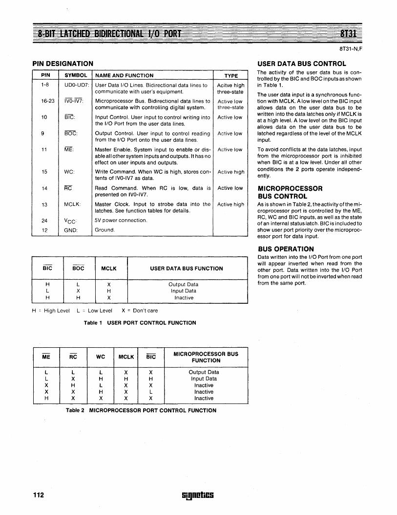
8-BIT EITCltED BIDIRECTIONAL 110 PORT
PIN DESIGNATION
PIN SYMBOL NAME AND FUNCTION TYPE
1-8 UDO-UD7: User Data 110 Lines. Bidirectional data lines to Acitve high communicate with user's equipment. th ree-state
16-23 IVO-IV7: Microprocessor Bus. Bidirectional data lines to Active low communicate with controlling digital system. th ree-state
10 BIC: Input Control. User input to control writing into Active low the 110 Port from the user data lines.
9 BOC: Output Control. User input to control reading Active low from the 110 Port onto the user data lines.
11 ME: Master Enable. System input to enable or dis- Active low able all other system inputs and outputs. It has no effect on user inputs and outputs.
15 WC: Write Command. When WC is high, stores con- Active high tents of IVO-IV7 as data.
14 RC Read Command. When RC is low, data is Active low presented on IVO-IV7.
13 MCLK: Master Clock. Input to strobe data into the Active high latches. See function tables for details.
24 VCC: 5V power connection.
12 GND: Ground.
-BIC BOC MCLK USER DATA BUS FUNCTION
H L X Output Data L X H Input Data H H X Inactive
H = High Level L = Low Level X = Don't care
Table 1 USER PORT CONTROL FUNCTION
- -BIC MICROPROCESSOR BUS ME RC WC MCLK
FUNCTION
L L L X X Output Data L X H H H Input Data X H L X X Inactive X X H X L Inactive H X X X X Inactive
Table 2 MICROPROCESSOR PORT CONTROL FUNCTION
112 !ii,gnotiC!i
8T31
8T31-N,F
USER DATA BUS CONTROL The activity of the user data bus is controlled by the BIC and BOC inputs as shown in Table 1.
The user data input is a synchronous function with MCLK. A low level on the BIC input allows data on the user data bus to be written into the data latches only if MCLK is at a high level. A low level on the BIC input allows data on the user data bus to be latched regardless of the level of the MCLK input.
To avoid conflicts at the data latches, input from the microprocessor port is inhibited when BIC is at a low level. Under all other conditions the 2 ports operate independently.
MICROPROCESSOR BUS CONTROL As is shown in Table 2, the activity ofthe microprocessor port is controlled by the ME, RC, WC and BIC inputs, as well as the state of an internal status latch. BIC is included to show user port priority over the microprocessor port for data input.
BUS OPERATION Data written into the liD Port from one port will appear inverted when read from the other port. Data written into the liD Port from one port will not be inverted when read from the same port.
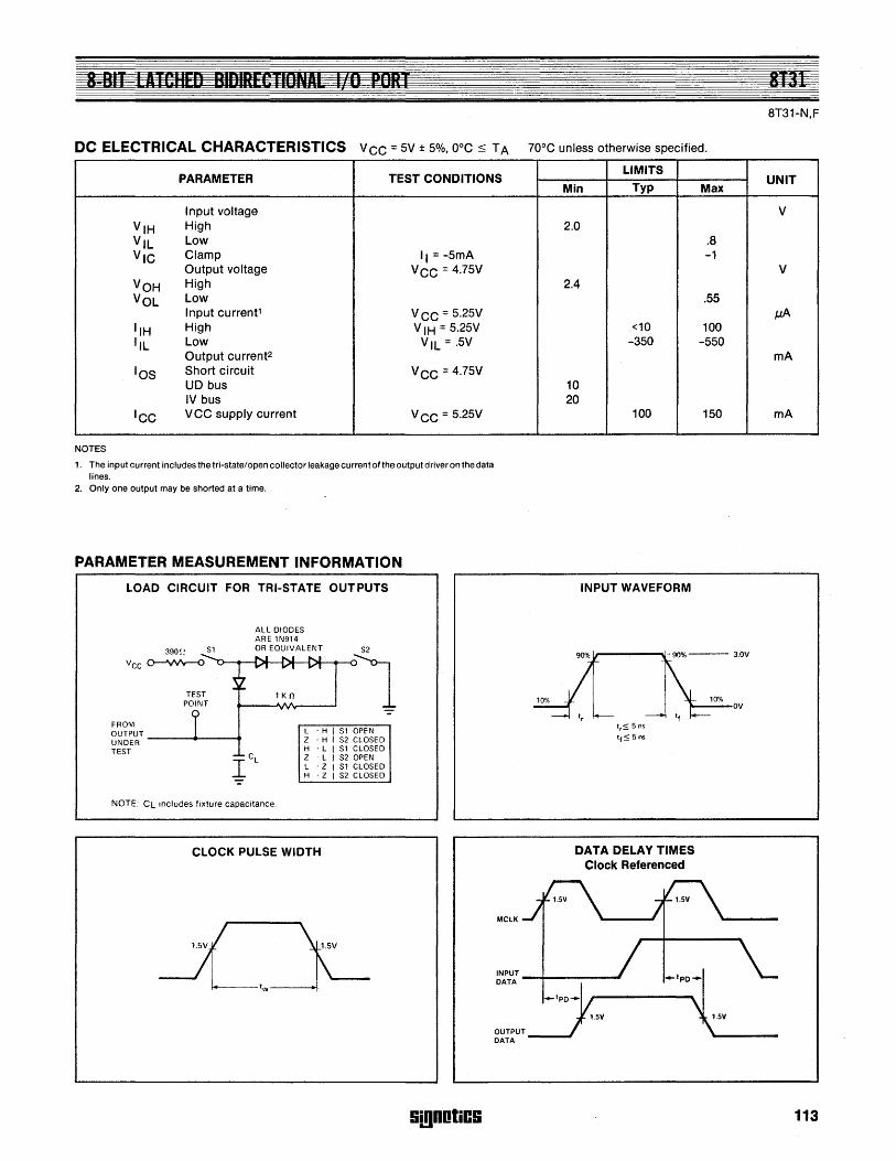
DC ELECTRICAL CHARACTERISTICS vee = 5V ± 5%, ooe ::; T A 700 e unless otherwise specified.
PARAMETER TEST CONDITIONS LIMITS
Typ
Input voltage
VIH High
VIL Low
Vie elamp II = -5mA Output voltage Vee = 4.75V
VOH High
VOL Low Input current1 Vee = 5.25V
IIH High VIH = 5.25V IlL Low VIL=·5V
Output current2
lOS Short circuit Vee = 4.75V UD bus IV bus
lee vee supply current Vee = 5.25V
NOTES
1. The input current includes the tri-state/open collector leakage current ofthe output driver on the data lines.
2. Only one output may be shorted at a time.
PARAMETER MEASUREMENT INFORMATION
LOAD CIRCUIT FOR TRI-STATE OUTPUTS
FROM OUTPUT UNDER TEST
ALL DIODES ARE 1N914 OR EQUIVALENT
1 KO
L ·H Z ·H H ·L
r CL z ·L L 'Z H 'Z
NOTE: CL Includes fixture capacitance
CLOCK PULSE WIDTH
Sl OPEN S2 CLOSED Sl CLOSED S2 OPEN Sl CLOSED S2 CLOSED
!ii!lDOliC9
MCLK
Min
2.0
2.4
<10 -350
10 20
100
INPUT WAVEFORM
DATA DELAY TIMES Clock Referenced
Max
.B -1
.55
100 -550
150
~:~:--~--------- --'PO--
BT31-N,F
UNIT
V
V
IJ.A
rnA
rnA
113
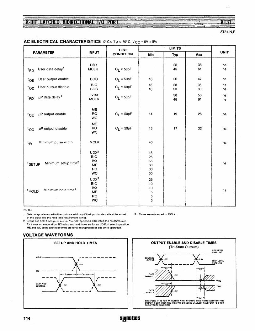
8T31-N,F
AC ELECTRICAL CHARACTERISTICS O°C::; TA ~ 70°C, VCC = 5V ± 5%
TEST LIMITS PARAMETER INPUT CONDITION Min Typ Max
UNIT
UOX 25 38 ns
tpo User data delay 1 MCLK C L = 50pF 45 61 ns
tOE User output enable BOC CL = 50pF 18 26 47 ns
too User output disable BIC
CL = 50pF 18 28 35 ns
BOC 16 23 33 ns
tpo J1P data delay 1 Ivax
CL = 50pF 38 53 ns
MCLK 48 61 ns
ME
tOE J1P output enable RC CL :: 50pF WC
14 19 25 ns
ME
too J1P output disable RC WC
CL = 50pF 13 17 32 ns
tw Minimum pulse width MCLK 40 ns
UOX3 15 BIC 25
tSETUP Minimum setup time 2 IVX 55 ME 30 ns
RC 30 WC 30
UDX3 25 BIC 10
t HOLD Minimum hold time 2 IVX 10 ME 5
ns
RC 5 WC 5
NOTES
1. Data delays referenced to the clock are valid only if the input data is stable at the arrival 3. Times are referenced to MClK. of the clock and the hold time requirement is met.
2. Set up and hold times given are for "normal" operation. BIC setup and hold times are for a user write operation. RC setup and hold times are for an 1/0 Port select operation. ME and WC setup and hold times are for a microprocessor bus write operation.
VOLTAGE WAVEFORMS
SETUP AND HOLD TIMES
114
MClK -------_
BIC
DATA AND CONTROL
,---------I
SmnOliC9
OUTPUT ENABLE AND DISABLE TIMES (Tri-State Outputs)
lOW lEVEL ENABLING ,.....---
1.5V HIGH lEVEL ENABLING I' 'I L'--I-----J I '-----
toE-i ~tOD..j ~o+,o-~ I I I
OO~~ I I I
~~~~~----------~I~~~~~~VOL
DATA OOTPUT2
I .,....,...;,.....,..;, ........ """""'.--------!,-l.....r'~..,....,... ~VOH I I I I--tOD~
WAVEFORM #1 IS FOR AN OUTPUT WITH INTERNAL CONDITIONS SUCH THAT THE OUTPUT IS LOW WHEN THE TRI·STATE DRIVER IS ENABLED. WAVEFORM "2 IS FOR THE OPPOSITE CONDITION.
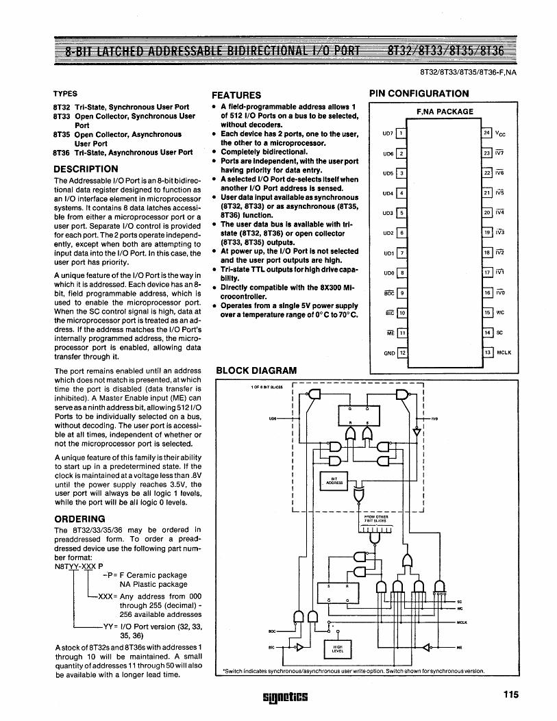
8 Sif LAICHED ADIlRESSABI E BIDIRECTIONAL I tr-PORT ST3? ST33 8135 BI36
TYPES
8T32 Tri-State, Synchronous User Port 8T33 Open Collector, Synchronous User
Port 8T35 Open Collector, Asynchronous
User Port 8T36 Trl-State, Asynchronous User Port
DESCRIPTION The Addressable I/O Port is an B-bit bidirectional data register designed to function as an I/O interface element in microprocessor systems. It contains B data latches accessible from either a microprocessor port or a user port. Separate I/O control is provided for each port. The 2 ports operate independently, except when both are attempting to input data into the I/O Port. In this case, the user port has priority.
A unique feature of the I/O Port is the way in which it is addressed. Each device has an Bbit, field programmable address, which is used to enable the microprocessor port. When the SC control signal is high, data at the microprocessor port is treated as an address. If the address matches the I/O Port's internally programmed address, the microprocessor port is enabled, allowing data transfer through it.
The port remains enabled until an address which does not match is presented, at which time the port is disabled (data transfer is inhibited). A Master Enable input (ME) can serve as a ninth address bit, allowing 5121/0 Ports to be individually selected on a bus, without decoding. The user port is accessible at all times, independent of whether or not the microprocessor port is selected.
A unique feature of this family is their ability to start up in a predetermined state. If the clock is maintained at a voltage less than .BV until the power supply reaches 3.5V, the user port will always be all logic 1 levels, while the port will be all logic a levels.
ORDERING The BT32/33/35/36 may be ordered in preaddressed form. To order a preaddressed device use the following part number format: NBTYY-XXX P
l -'P= F Ceramic package NA Plastic package
XXX= Any address from 000 through 255 (decimal) -256 available addresses
,---yy = I/O Port version (32, 33, 35,36)
A stock of BT32s and BT36s with add resses 1 through 10 will be maintained. A small quantity of addresses 11 through 50 will also be available with a longer lead time.
BT32/BT33/BT35/BT36-F ,NA
FEATURES • A field-programmable address allows 1
of 512 I/O Ports on a bus to be selected, without decoders.
• Each device has 2 ports, one to the user, the other to a microprocessor.
• Completely bidirectional. • Ports are Independent, with the user port
having priority for data entry. • A selected I/O Port de-selects Itself when
another I/O Port address Is sensed. • User data Input available as synchronous
(8T32, 8T33) or as asynchronous (8T3S, 8T36) function.
• The user data bus Is available with tristate (8T32, 8T36) or open collector (8T33, 8T3S) outputs.
• At power up, the I/O Port Is not selected and the user port outputs are high.
• Tri-state TTL outputs for high drive capability.
• Directly compatible with the 8X300 MIcrocontroller.
• Operates from a single SV power supply over a temperature range of 0° C to 70° C.
BLOCK DIAGRAM
PIN CONFIGURATION
F,NA PACKAGE
UD7 1
UD6 2
UD5 3
UD4 4
UD3 5
UD2 6
UD1 7
UDO 8
BoG 9
SiC 10
ME 11
GND 12
1 OF 8 lilT SLICES r-----------------,
BOC
I I I I I I I I
I I I I I I t I I I I J L_
~H++4~~++~-~
'---++-++---1 ......... - we
9------t+-__ H+-+++---+---MCLK
BIC --r~" __ -
24
23
22
21
20
19
'Switch indicates synchronous/asynchronous user write option. Switch shown for synchronous version.
limDOliCS
Vcc
IV7
iV6
iV5
iV4
iV3
iV2
iV1
IVO
WC
sc
MCLK
115
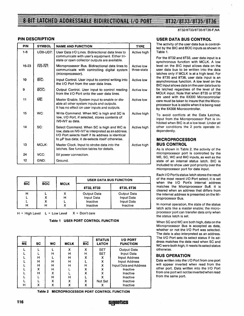
8 BIT LAICHED IDORI SSABEE BIUIREtTION#\[ I 0 PORT
PIN DESCRIPTION
PIN SYMBOL NAME AND FUNCTION TYPE
1-8 UDO-UD7: User Data 1/0 Lines. Bidirectional data lines to Active high communicate with user's equipment. Either tri-state or open collector outputs are available.
16-23 IVO-IV7: Microprocessor Bus. Bidirectional data lines to Active low communicate with controlling digital system th ree-state (microprocessor).
10 BIC: Input Control. User input to control writing into Active low the 1/0 Port from the user data lines.
9 BOC: Output Control. User input to control reading Active low from the 1/0 Port onto the user data lines.
11 ME: Master Enable. System input to enable or dis- Active low able all other system inputs and outputs. It has no effect on user inputs and outputs.
15 WC: Write Command. When WC is high and SC is Active high low, 110 Port, if selected, stores contents of IVO-IV7 as data.
14 SC: Select Command. When SC is high and WC is Active high low, data on IVO-IV7 is interpreted as an address. 110 Port selects itself if its address is identical to J.1.P bus data; it de-selects itself otherwise.
13 MCLK: Master Clock. Input to strobe data into the Active high latches. See function tables for details.
24 VCC: 5V power connection.
12 GND: Ground.
USER DATA BUS FUNCTION - --BIC BOC MCLK
8T32,8T33 8T3S,8T36
H L X Output Data Output Data L X H Input Data Input Data L X L Inactive Input Data H H X Inactive Inactive
H = High Level L = Low Level X = Don't care
Table 1 USER PORT CONTROL FUNCTION
STATUS 1/0 PORT - -ME SC WC MCLK BIC LATCH FUNCTION
L L L X X SET Output Data L L H H H SET Input Data ~ H L H X X Input Address L H H H L X Input Address L H H H H X Input Data and Address L X H L X X Inactive L H X L X X Inactive L L H H L X Inactive L L X X X Not Set Inactive H X X X X X Inactive
Table 2 MICROPROCESSOR PORT CONTROL FUNCTION
116 !ii!lDOliC9
BT32 BT33 BI35 8136 8T32/8T33/8T35/8T36-F,NA
USER DATA BUS CONTROL The activity of the user data bus is controlled by the BIC and BOC inputs as shown in Table 1.
For the 8T32 and 8T33, user data input is a synchronous function with MCLK. A low level on the BIC input allows data on the user data bus to be written into the data latches only if MCLK is at a high level. For the 8T35 and 8T36, user data input is an asynchronous function. A low level on the BIC input allows data on the user data bus to be latched regardless of the level of the MCLK input. Note that when 8T35 or 8T36 are used with the 8X300 Microcontroller care must be taken to insure that the Microprocessor bus is stable when it is being read by the 8X300 Microcontroller.
To avoid conflicts at the Data Latches, input from ,.the Microprocessor Port is inhibited when BIC is at a low level. Under all other conditions the 2 ports operate independently.
MICROPROCESSOR BUS CONTROL As is shown in Table 2, the activity of the microprocessor port is controlled by the ME, SC, WC and BIC inputs, as well as the state of an internal status latch. BIC is included to show user port priority over the microprocessor port for data input.
Each 1/0 Port's status latch stores the result of the most recent 110 Port select; it is set when the 110 Port's internal address matches the Microprocessor Bu~. It is cleared when an address that differs from the internal address is presented on the Microprocessor Bus.
In normal operation, the state of the status latch acts like a master enable; the microprocessor port can transfer data only when the status latch is set.
When SC and WC are both high, data on the Microprocessor Bus is accepted as data, whether or not the 1/0 Port was selected. The data is also interpreted as an address. The 1/0 Port sets its select status if its address matches the data read when SC and WC were both high; it resets its select status otherwise.
BUS OPERATION Data written into the 1/0 Port from one port will appear inverted when read from the other port. Data written into the 1/0 Port from one port will not be inverted when read from the same port.
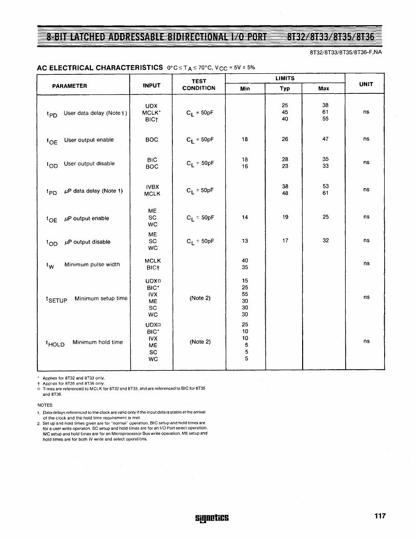
8 BIT LATCHED ADDRESSABLE BIDIRECTION#\L I 0 PORT
AC ELECTRICAL CHARACTERISTICS O°C:::; T A:::; 70°C, VCC = 5V ± 5%
PARAMETER
tpD User data delay (Note 1 )
tOE User output enable
too User output disable
tpD J1P data delay (Note 1)
tOE IlP output enable
too IlP output disable
tw Minimum pulse width
tSETUP Minimum setup time
tHOLD Minimum hold time
• Applies for 8T32 and 8T33 only. t Applies for 8T35 and 8T36 only.
TEST INPUT CONDITION
UDX MCLK* CL = 50pF BICt
BOC CL = 50pF
BIC CL = 50pF BOC
IVBX CL = 50pF MCLK
ME SC CL = 50pF WC
ME SC CL = 50pF WC
MCLK BICt
UDXo BIC· IVX
(Note 2) ME SC WC
UDXo BIC* IVX
(Note 2) ME SC WC
o Times are referenced to MCLK for 8T32 and 8T33, and are referenced to BIC for 8T35 and 8T36.
NOTES:
1. Data delays referenced to the clock are valid only if the input data is stable at the arrival of the clock and the hold time requirement is met.
2. Set up and hold times given are for "normal" operation. BIC setup and hold times are for a user write operaton. SC setup and hold times are for an I/O Port select operation. WC setup and hold times are for an Microprocessor Bus write operation. ME setup and hold times are for both IV write and select operations.
Si!lDOliC9
Min
18
18 16
14
13
40 35
15 25 55 30 30 30
25 10 10 5 5 5
8132 8T33 8T35 8136 8T32/8T33/8T35/8T36-F, NA
LIMITS
Typ Max UNIT
25 38 45 61 ns 40 55
26 47 ns
28 35 23 33
ns
38 53 48 61
ns
19 25 ns
17 32 ns
ns
ns
ns
117
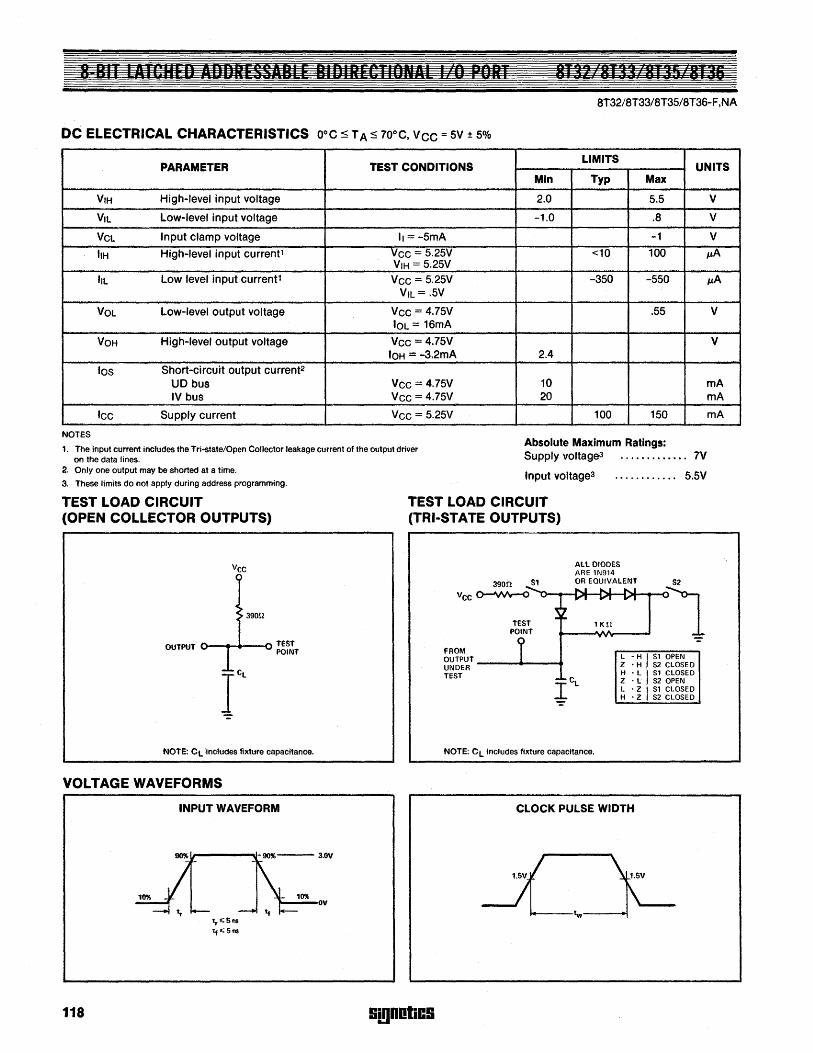
8 BIT LATCHED ADDRESSABI E BIDIRECTIONAL I (J PORT 8132 8Tl3 8135 813& 8T32/8T33IBT35/BT36-F,NA
DC ELECTRICAL CHARACTERISTICS O°C ~ TA ~ 70°C, Vee = 5V ± 5%
PARAMETER TEST CONDITIONS LIMITS
UNITS Min Typ Max
V1H High-level input voltage 2.0 5.5
Vil Low-level input voltage -1.0 .B
Vel Input clamp voltage II = -SmA -1
ItH High-level input current1 Vee = 5.25V <10 100 VIH = 5.25V
III Low level input current1 Vee = 5.25V -350 -550 VIL = .5V
VOL Low-level output voltage Vee = 4.75V .55 10L = 16mA
VOH High-level output voltage Vee = 4.75V 10H = -3.2mA 2.4
los Short-circuit output current2
UD bus Vee = 4.7SV 10 IV bus Vee = 4.75V 20
Icc Supply current Vee = 5.25V 100 150
NOTES
1. The input current includes the Tri·state/Open Collector leakage current of the output driver on the data lines.
Absolute Maximum Ratings: Supply voltage3 .. • • • .. • • • ... 7V
2. Only one output may be shorted at a time.
3. These limits do not apply during address programming.
TEST LOAD CIRCUIT (OPEN COLLECTOR OUTPUTS)
Vee (
~
~> 390U
NOTE: CL lncludes fixture capacitance.
VOLTAGE WAVEFORMS
INPUT WAVEFORM
118
t,~5ns
1f,,"5ns
"----ov
Input voltage3 . .. • • .. .. ... 5.5V
TEST LOAD CIRCUIT (TRI-STATE OUTPUTS)
!ii!lDDliC!i
All DIODES ARE 1N914 OR EOUIVAl£NT
~RDM
~~6~~T ---t-----t TEST
NOTE: CL includes fixture capacitance.
lK!!
L • H I S1 OPEN Z • H S2 CLOSED H • L I S1 CLOSED Z • L f S2 OPEN L • Z I S1 CLOSED H • Z S2 CLOSED
CLOCK PULSE WIDTH
V
V
V
p.A
p.A
V
V
rnA rnA
rnA
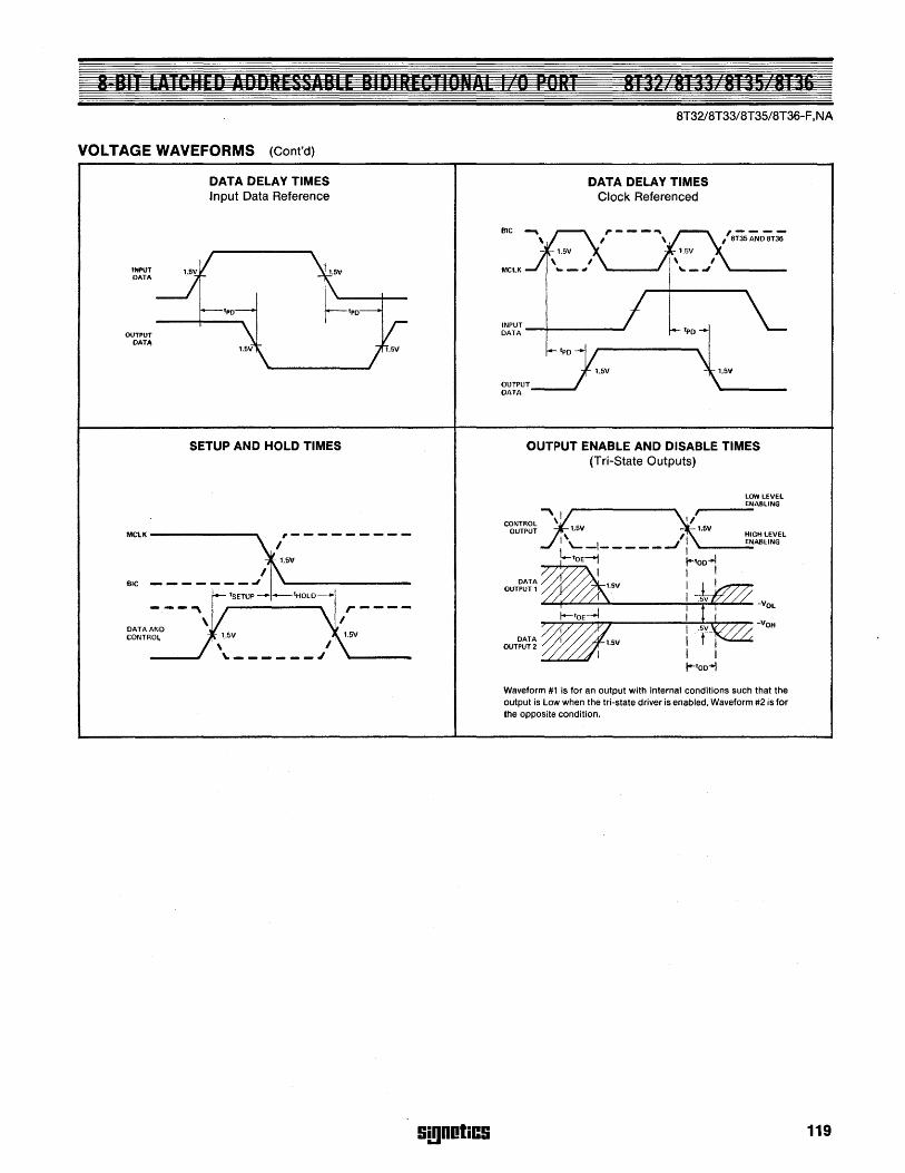
8 BII LAICHED ADDRESSABLE BIOI RECIIONAL I 0 PORI 8112 8111 8I1S 8136
VOLTAGE WAVEFORMS (Cont'd)
lNPt1T DATA
OUTPUT DATA
DATA DELAY TIMES Input Data Reference
SETUP AND HOLD TIMES
1\IICt,K , - - - - - - - - -
Ene _________ J
DATA AND CONTROL,
I
S!!]DotiC!i
8T32/8T33/8T35/8T36-F ,NA
BtC
MClK
DATA DELAY TIMES Clock Referenced
~:~; -+------'
OUTPUT ENABLE AND DISABLE TIMES (Tri-State Outputs)
LOW LEVEL ENABLING
CONTROL \ 1/ =*' *,----OUTPUT 1.5V 1.5V
DATA OUTPUT 1
DATA OUTPUT 2
, \ I j ~~~~~~iL L~-l-----.J j -------
~~~tO~E-1 ~~D~ 1 I I
I 1
"-'-+-'-'--'--....a... ____ --;.! ~~""-'~ -VOL
, .,...,...,....~-r!'r7"------;.1 ~-,.I,...,....~ -VOH
I I I .... tOD+1
Waveform #1 is for an output with Internal conditions such that the output is Low when the tri-state driver is enabled. Waveform #2 is for the opposite condition.
119
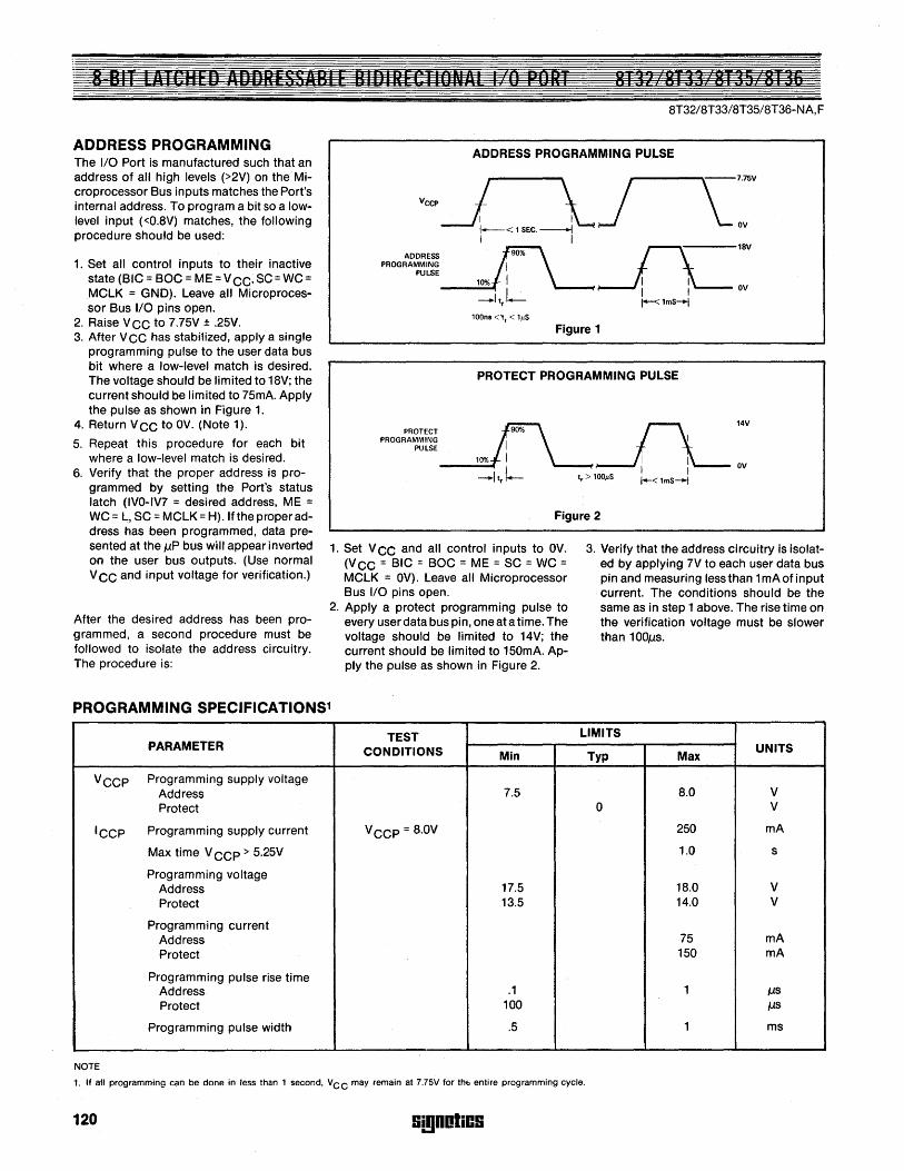
8 BIT EnICHED ADDRESSABI F BIDIRECTIl)NAL I () PORT 8T3' 8T33 8135 8T36
ADDRESS PROGRAMMING The I/O Port is manufactured such that an address of all high levels (>2V) on the Microprocessor Bus inputs matches the Port's internal address. To program a bit so a lowlevel input «O.BV) matches, the following procedure should be used:
1. Set all control inputs to their inactive state (BIC = BOC = ME = V CC' SC = WC = MCLK = GND). Leave all Microprocessor Bus I/O pins open.
2. Raise V CC to 7.75V ± .25V. 3. After V CC has stabilized, apply a single
programming pulse to the user data bus bit where a low-level match is desired. The voltage should be limited to 1BV; the current should be limited to 75mA. Apply the pulse as shown in Figure 1.
4. Return V CC to OV. (Note 1).
5. Repeat this procedure for each bit where a low-level match is desired.
6. Verify that the proper address is programmed by setting the Port's status latch (IVO-IV7 = desired address, ME = WC = L, SC = MCLK = H). Ifthe proper address has been programmed, data presented at the I1P bus will appear inverted on the user bus outputs. (Use normal V CC and input voltage for verification.)
After the desired address has been programmed, a second procedure must be followed to isolate the address circuitry. The procedure is:
BT32/BT33/BT35/BT36-NA, F
ADDRESS PROGRAMMING PULSE
Vcep ~7'75V
I. <,~c \- 'v
ADDREss~1 90% I JL 18V PROGRAMMING I
PULSE 10% I I I OV
L I I -Itr !-<1mS-+j
Figure 1
PROTECT PROGRAMMING PULSE
JL14V
PROTECT 90% PROGRAMMING~ I PULSE
10% I I I OV
I I I -I tr - t r > 100"s 1-< 1mS-l
Figure 2
1. Set V CC and all control inputs to OV. (VCC = BIC = BOC = ME = SC = WC = MCLK = OV). Leave all Microprocessor Bus I/O pins open.
2. Apply a protect programming pulse to every user data bus pin, oneata time. The voltage should be limited to 14V; the current should be limited to 150mA. Apply the pulse as shown in Figure 2.
3. Verify that the address circuitry is isolated by applying 7V to each user data bus pin and measuring less than 1mAofinput current. The conditions should be the same as in step 1 above. The rise time on the verification voltage must be slower than 10011s.
PROGRAMMING SPECIFICATIONS1
TEST LIMITS PARAMETER CONDITIONS Min Typ Max
UNITS
VCCP Programming supply voltage B.O V Address 7.5
Protect 0 V
ICCp Programming supply current VCCP = B.OV 250 rnA
Max time V CCP > 5.25V 1.0 s
Programming voltage Address 17.5 1B.0 V Protect 13.5 14.0 V
Programming current Address 75 rnA Protect 150 rnA
Programming pulse rise time Address .1 1 I1S Protect 100 I1S
Programming pulse width .5 1 ms
NOTE
1. If all programming can be done in less than 1 second, Vee may remain at 7.7SV for thb entire programming cycle.
120 !ii!lDOliC!i
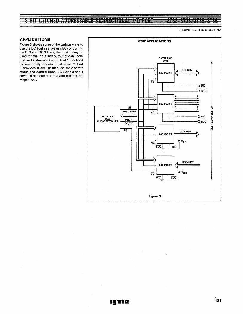
8 BIT lATCHED AODRESSABL E BIDIREUIIONAI I 0 PORT 8132 8133 8135 8136
APPLICATIONS Figure 3 shows some of the various ways to use the I/O Port in a system. By controlling the BIC and BOC lines, the device may be used for the input and output of data, control, and status signals. I/O Port 1 functions bidirectionally for data transfer and I/O Port 2 provides a similar function for discrete status and control lines. I/O Ports 3 and 4 serve as dedicated output and input ports, respectively.
[8
jVBO-IVB7
( SfGNETICS
'of MCLK. eX300 MICRO CONTROLLER
sC,wc
RB
~
9i!1DOliC!i
8T32 APPLICATIONS
~
\ -V
r--+" ME
\ -y
ME
... 1>
ME
SIGNETICS BT32
I/O PORT
I I
I/O PORT
I I
I/O PORT
BO~
\ -y I/O PORT
ME
<
•
BIC
~
BIC~ BOC
Figure 3
BT32/BT33/BT35/BT36-F, NA
UDO-UD7
UDO-UD7
VCC
UDO-UD7
VCC
> -. ..... -. .....
•
.... ~
.... .....
..... >
V
z o ~ u w Z Z o u ex: w en ::>
121
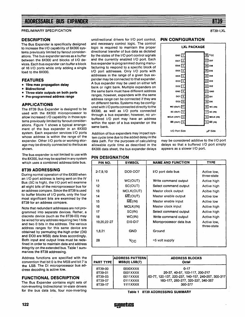
PRELIMINARY SPECIFICATION
DESCRIPTION The Bus Expander is specifically designed to increase the I/O capability ofaX300 systems previously limited by fanout considerations. The bus expander serves as a buffer between the aX300 and blocks of I/O devices. Each bus expander can buffer a block of 16 I/O ports while only adding a single load to the aX300.
FEATURES • 15ns max propagation delay • Bidirectional • Three-state outputs on both ports • Pre-programmed address range
APPLICATIONS The aT39 Bus Expander is designed to be used with the aX300 microprocessor to allow increased I/O capability in those systems previously limited by fanout considerations. Figure 1 shows a typical arrangement of the bus expander in an aX300 system. Each expander services I/O ports whose address is within the range of the expander. Other I/O ports or working storage may be directly connected to the bus as shown.
unidirectional drivers for I/O port control, and necessary control logic. The control logic is required to maintain the proper directional transfer of bus data as dictated by the states of the I/O port control signals and the currently enabled I/O port. Each bus expander is programmed during manufacturing to respond to a specific block of 1/0 port addresses. Only I/O ports with addresses in the range of a given bus expander may be connected to that expander. A bus expander may be used on either left bank or right bank. Multiple expanders on the same bank must have different address ranges; however, expanders with the same address range can be connected if they are on different banks. Systems may be configured with I/O ports connected directly to the aX300, as well as I/O ports connected through a bus expander; however, no unbuffered I/O port may have an address within the span of a bus expander on the same bank.
Addition of bus expanders may impact system cycle time due to the added delay in the data path. For the purposes of calculating allowable cycle time as described in the aX300 data sheet, the bus expander delays
aT39-I,XL
PIN CONFIGURATION
I,XL PACKAGE
110 Port Side IJ,PSide
may be considered additive to the I/O port delays so that a buffered I/O port simply appears as a slower I/O port.
The bus expander is not limited to use with the aX300, but may be applied in any system PIN DESIGNATION which uses a combined address/data bus.
ST39 ADDRESSING During normal operation of the aX300 when an I/O port address is being sent on the IV Bus (SC is high), the I/O port will examine all eight bits of the microprocessor bus for an address compare. Since the aT39 is used to buffer blocks of I/O ports, only the four most significant bits are examined by the 8T39 for an address compare.
Note that redundant addresses are not programmed into separate devices. Rather, a discrete device (such as the aT39-03) may be wired for any address requiring two 1 bits and two 0 bits in the address. The various address ranges for this same device are obtained by permuting the high order (010 and 000 are MSB) data lines accordingly. Both input and output lines must be redefined in order to maintain data and address integrity on the extended bus. Table 1 summarizes the aT39 addressing.
Address functions are specified with the convention that bit 0 is the MSB and bit 7 is the LSB. The 01 microprocessor bus address decoding is active low.
FUNCTIONAL DESCRIPTION The Bus Expander contains eight sets of non-inverting bidirectional tri-state drivers for the bus data bits, four non-inverting
122
PIN NO.
2-7,9,10
11
12
13
14
15
16
17
1a
19,20,22-27
1,a,21
2a
PART TYPE
aT39-00 aT39-01 aT39-03 aT39-07 aT39-17
SYMBOL NAME AND FUNCTION TYPE
000-007 110 port data bus Active low, three-state
WC(OUT) Write command output Active high
SC(OUT) Select command output Active high
MCLK(OUT) Master clock output Acitve high
ME(OUT) Master enable output Active low
ME(lN) Master enable input Active low
MCLK(IN) Master clock input Active high
SC(IN) Select command output Active high
WC(IN) Write command output Active high
010-017 Microprocessor data bus Active low, three-state
GNO Ground
VCC +5 volt supply
ADDRESS PATTERN ADDRESS BLOCKS MSB(O) LSB(7) Octal
OOOOXXXX 0-17 0001XXXX 20-37, 40-57, 100-117, 200-217 0011XXXX 60-77, 120-137, 220-237, 140-157, 240-257, 300-317 0111XXXX 160-177. 260-277, 320-337, 340-357 1111XXXX 360-377
Table 1 8T39 ADDRESSING SUMMARY
SmOOliCS
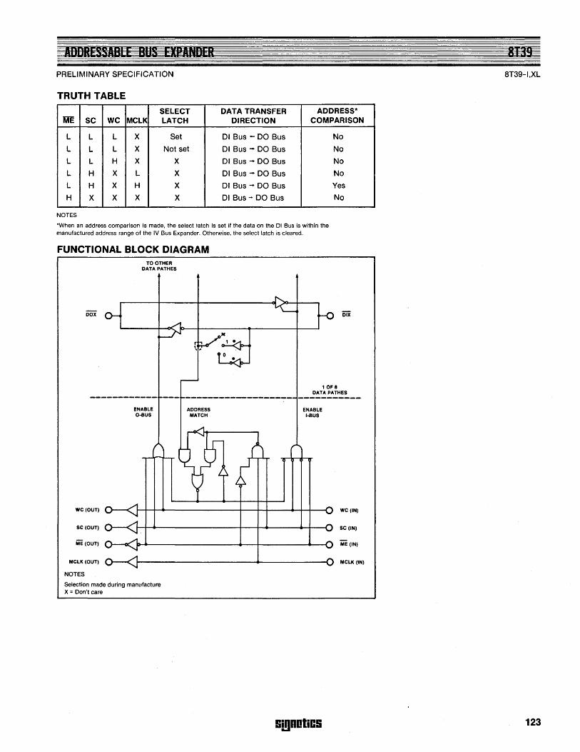
PRELIMINARY SPECIFICATION
TRUTH TABLE
SELECT DATA TRANSFER ADDRESS* ME SC WC MCLK LATCH DIRECTION COMPARISON
L L L X Set DI Bus - DO Bus No
L L L X Not set DI Bus - DO Bus No
L L H X X DI Bus - DO Bus No
L H X L X DI Bus - DO Bus No
L H X H X DI Bus - DO Bus Yes
H X X X X DI Bus - DO Bus No
NOTES
'When an address comparison is made, the select latch is set if the data on the DI Bus is within the manufactured address range of the IV Bus Expander. Otherwise, the select latch is cleared.
FUNCTIONAL BLOCK DIAGRAM
WC(OUT)
SC (OUT)
ME (OUT)
MCLK (OUT)
NOTES
TO OTHER DATA PATHES
ENABLE O-BUS
Selection made during manufacture X = Don't care
10F8 DATA PATHES
ENABLE I-BUS
Si!)notics
WC(IN)
SC(IN)
ME (IN)
MCLK (IN)
8T39-I,XL
123
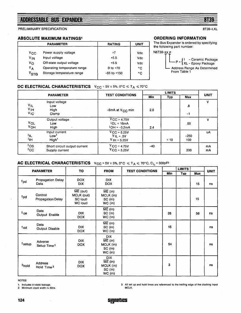
PRELIMINARY SPECIFICATION
ABSOLUTE MAXIMUM RATINGS1 PARAMETER
VCC Power supply voltage
VIN Input voltage
Vo Off-state output voltage
TA Operating temperature range
TSTG Storage temperature range
RATING UNIT
+7 Vdc
+5.5 Vdc
+5.5 Vdc
o to +70 °c -65 to +150 °c
ST39-I,XL
ORDERING INFORMATION The Bus Expander is ordered by specifying the following part number:
NST39-xx p
~L _ { I - Ceramic Package P - XL - Epoxy Package
Address Range As Determined From Table 1
DC ELECTRICAL CHARACTERISTICS Vec = 5V ± 5%, O°C ~ T A ~ 70°C
PARAMETER TEST CONDITIONS LIMITS
UNIT Min Typ Max
Input voltage V VIL Low .S VIH High -5mA at V CC min 2.0 VIC Clamp -1
Output voltage VCC = 4.75V V VOL Low IOL = 16mA .55 VOH High 10H = -3.2mA 2.4
Input current VCC = 5.25V uA IlL Low1 VIL = .5V -250 IIH High1 V IH = 5.25V < 10 100
lOS Short circuit output current V CC = 4.75V -40 mA ICC Supply current VCC = 5.25V 200 rnA
AC ELECTRICAL CHARACTERISTICS VCC = 5V ± 5%, O°C ~ TA ~ 70°C, CL = 300pF2
PARAMETER TO
tpd Propagation Delay DOX Data DIX
ME (out)
tpd Control MCLK (out) Propagation Delay SC (out)
WC (out)
Data toe Output Enabl.e DIX
DOX
Data tod Output Disable DIX
DOX
Adverse DIX tsetup Setup Time3 DOX
Address DIX thold Hold Time 3 DOX
NOTES
1. Includes tri-state leakage. 2. Minimum clock width = 50ns.
124
FROM
DIX DOX
ME (in) MCLK (in)
SC (in) WC (in)
ME (in) SC (in) WC (in)
ME (in) SC (in) WC (in)
DIX ME (in)
MCLK (in) SC (in) WC (in)
DIX ME (in)
MCLK (in) SC (in) WC (in)
TEST CONDITIONS LIMITS
UNIT Min Typ Max
15 ns
15
2S 56 ns
15 ns
54 ns
3 ns
3. All set up and hold times are referenced to the trailing edge of the clocking input MCLK.
!ii!lDOliC!i
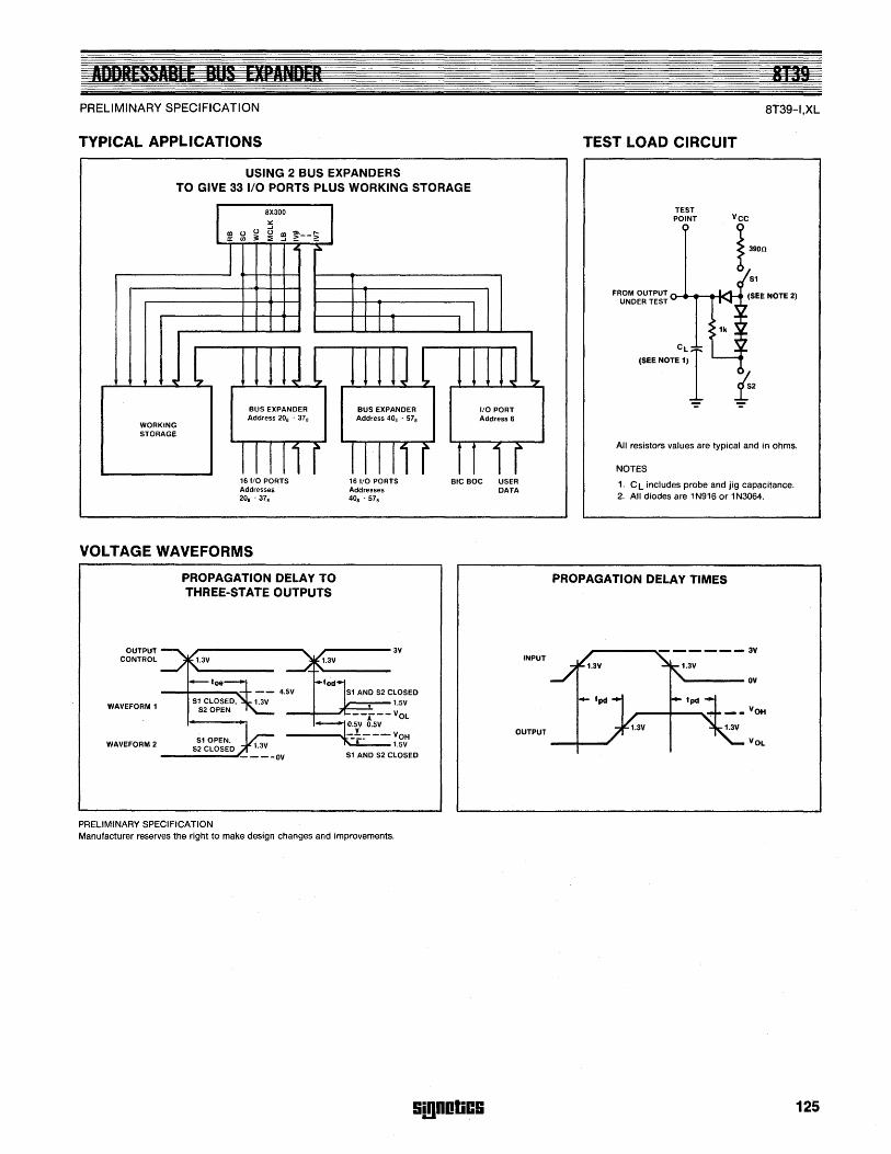
ADDRESSABLE BUS EXPANDER PRELIMINARY SPECIFICATION
TYPICAL APPLICATIONS
USING 2 BUS EXPANDERS TO GIVE 33 1/0 PORTS PLUS WORKING STORAGE
WORKING STORAGE
BUS EXPANDER Address 20. . 37.
161/0 PORTS Addresses 20 •. 37.
VOLTAGE WAVEFORMS
OUTPUT CONTROL
WAVEFORM 1
PROPAGATION DELAY TO THREE-STATE OUTPUTS
BUS EXPANDER Address 40, . 57.
161/0 PORTS Addresses 40 •. 57,
3V
1.5V
--r--VOL 0.5V 0.5V
1/0 PORT Address 6
BIC BOC USER DATA
INPUT
-}.~--.VOH OUTPUT S10PEN. i" 1.5V WAVEFORM 2
S2 CLOSED Sl AND S2 CLOSED
PRELIMINARY SPECIFICATION Manufacturer reserves the right to make deSign changes and improvements.
9i!1001iCS
TEST LOAD CIRCUIT
TEST POINT
CL
(SEE NOTE 1) I
8T39
BT39-I,XL
All resistors values are typical and in ohms.
NOTES
1. C L includes probe and jig capacitance. 2. All diodes are 1 N916 or 1 N3064.
PROPAGATION DELAY TIMES
OV
VOL
125
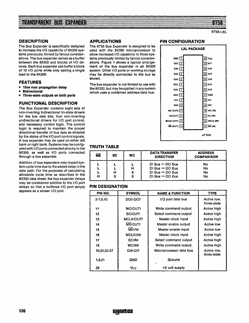
8T58-',XL
DESCRIPTION APPLICATIONS PIN CONFIGURATION The Bus Expander is specifically designed to increase the 1/0 capability of 8X300 systems previously limited by fanout consider· ations. The bus expander serves as a buffer between the 8X300 and blocks of 1/0 de· vices. Each bus expander can buffer a block of 16 1/0 ports while only adding a single load to the 8X300.
The 8T39 Bus Expander is designed to be used with the 8X300 microprocessor to allow increased 110 capability in those systems previously limited by fanout considerations. Figure 1 shows a typical arrangement of the bus expander in an 8X300 system. Other 1/0 ports or working storage may be directly connected to the bus as shown.
I,XL PACKAGE
FEATURES • 15ns max propagation delay • Bidirectional • Three-state outputs on both ports
FUNCTIONAL DESCRIPTION The Bus Expander contains eight sets of non-inverting bidirectional tri-state drivers for the bus data bits, four non-inverting undirectional drivers for 110 port control, and necessary control logic. The control logiC is required to maintain the proper directional transfer of bus data as dictated by the states of the 1/0 port control signals. A bus expander may be used on either left bank or right bank. Systems may be configured with 1/0 ports connected directly to the 8X300, as well as 1/0 ports connected through a bus expander.
Addition of bus expanders may impact system cycle time due to the added delay in the data path. For the purposes of calculating allowable cycle time as described in the 8X300 data sheet, the bus expander delays may be considered additive to the 110 port
The bus expander is not limited to use with the 8X300, but may be applied in any system which uses a combined addressldata bus.
TRUTH TABLE
ME SC WC DATA TRANSFER
DIRECTION
L L L 01 Bus - DO Bus L L H 01 Bus - DO Bus L H X 01 Bus - DO Bus H X X 01 Bus - DO Bus
delays so that a buffered I/O port simply PIN DESIGNATION appears as a slower 110 port.
PIN NO. SYMBOL NAME & FUNCTION
2-7,9,10 000-007 flO port data bus
11 WC(OUT) Write command output
12 SC(OUT) Select command output
13 MCLK(OUT) Master clock input
14 ME(OUT) Maste'r enable output
15 ME(lN) Master enable input
16 MCLK(lN) Master clock input
17 SC(lN) Select command output
18 WC(lN) Write command output
19,20,22-27 010-017 Microprocessor data bus
1,8,21 GND Ground .,
28 Vee +5 volt supply
126 Si!lDlliGS
IlP Side
ADDRESS COMPARISON
No No No No
TYPE
Active low, three-state
Active high
Active high
Active high
Active low
Active low
Actfve high
Active high
Active high
Active low, three-state
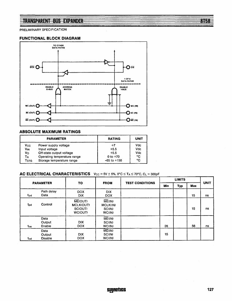
PRELIMINARY SPECIFICATION
FUNCTIONAL BLOCK DIAGRAM
WC(OUT)
SC(OUT)
ME (OUT)
TO OTHER DATA PATHS
ABSOLUTE MAXIMUM RATINGS
PARAMETER
Vee Power supply voltage VIN Input voltage Va Off-state output voltage TA Operating temperature range TSTG Storage temperature range
RATING
+7 +5.5 +5.5
o to +70
10F8 DATA PATHS
WCIIN)
SC (IN)
ME (IN)
UNIT
Vdc Vdc Vdc °C
-65 to +150 °C
AC ELECTRICAL CHARACTERISTICS Vee == 5V ± 5%, O°C ~ TA ~ 70°C, CL == 300pF
PARAMETER TO FROM TEST CONDITIONS
Path delay DOX DIX tpd Data DIX DOX
ME(OUT) ME(lN) tpd Control MCLK(OUT) MCLK(lN)
SC(OUT) SC(lN) WC(OUT) WC(lN)
Data ME(lN) Output DIX SC(lN)
toe Enable DOX WC(lN)
Data ME(lN) Output DIX SC(lN)
tod Disable DOX WC(lN)
liillBlllies
LIMITS UNIT
Min Typ Max
15 ns
15 ns
28 56 ns
15
127
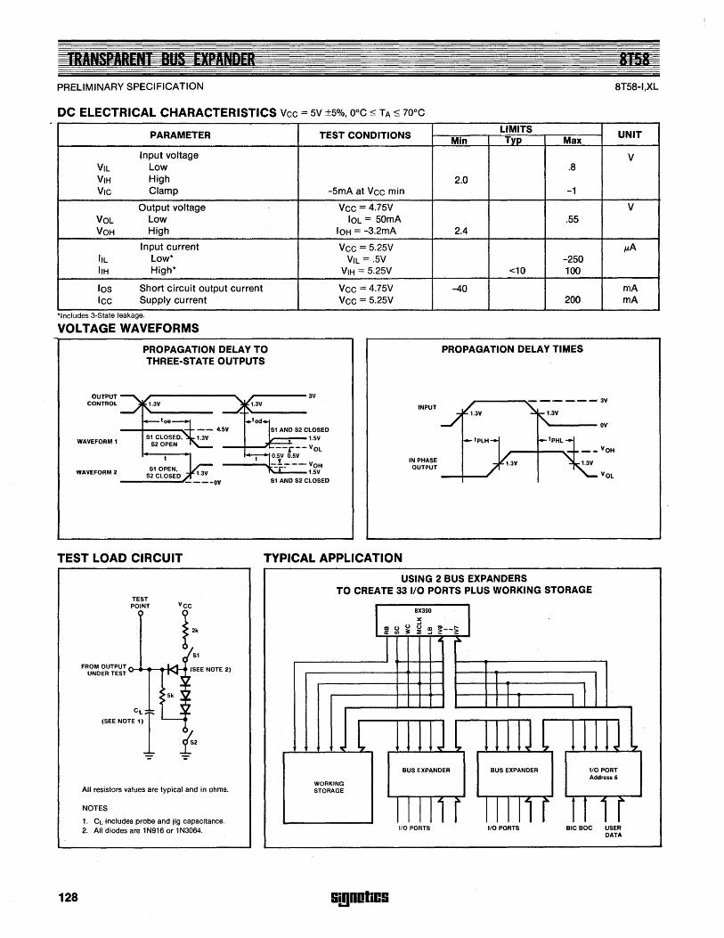
PRELIMINARY SPECIFICATION BT5B-I,XL
DC ELECTRICAL CHARACTERISTICS Vee = 5V ±5%, O°C ::; TA ::; 70°C
PARAMETER TEST CONDITIONS LIMITS UNIT
Min Typ Max
Input voltage V VIL Low .B VIH High 2.0 VIC Clamp -SmA at Vee min -1
Output voltage Vee = 4.75V V VOL Low 10L = 50mA .55 VOH High 10H = -3.2mA 2.4
Input current Vee = S.2SV p.A IlL Low* VIL = .SV -250 IIH High* VIH = S.2SV <10 100
los Short circuit output current Vee = 4.75V -40 rnA Icc Supply current Vee = 5.25V 200 rnA
'Includes 3-State leakage.
VOLTAGE WAVEFORMS
PROPAGATION DELAY TO THREE-STATE OUTPUTS
PROPAGATION DELAY TIMES
OUTPUT CONTROL
WAVEFORM 1
WAVEFORM 2
TEST LOAD CIRCUIT
_----3V
\,---=-- 1.SV
---+-JL.._-r -- VOL O.SV o.SV
----c-:.!.-:---- VOH r 1.SV
S1 AND S2 CLOSED
INPUT
IN PHASE OUTPUT
TYPICAL APPLICATION
USING 2 BUS EXPANDERS
"'----oV
TO CREATE 33//0 PORTS PLUS WORKING STORAGE
128
TEST POINT
CL
(SEE NOTE 111_ _ t, All resistors values are typical and in ohms.
NOTES
1. CL includes probe and jig capacitance. 2. All diodes are 1N916 or 1N3064.
WORKING STORAGE
9i!1DOliC9
BUS EXPANDER
I/O PORTS
BUS EXPANDER
I/O PORTS
I/O PORT Address 6
BIC BOC USER DATA
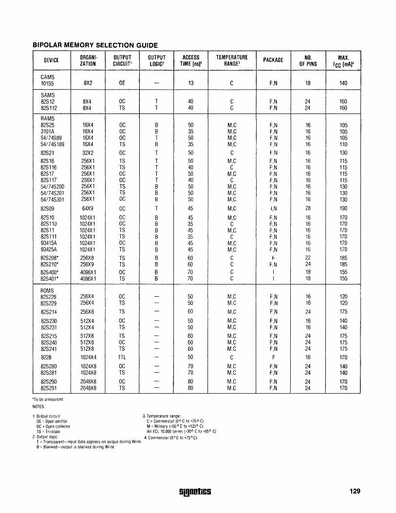
BIPOLAR MEMORY SELECTION GUIDE
DEVICE
CAMS 10155
SAMS 82S12 82S112
RAMS 82S25 3101A 541 74S89 54/74S189 82S?1 82S16 82S116 82S17 82S117 54/74S200 54/74S201 54/74S301
82S09
82S10 82S110 82S11 82S 111 93415A 93425A
82S208'" 82S21 0'" 82S400'" 82S401'"
ROMS 82S226 82S229
82S214
82S230 82S231
82S215 82S240 82S241
8228
82S280 82S281
82S290 82S291
'To be announced
NOTES
ORGAN I· ZATION
8X2
8X4 8X4
16X4 16X4 16X4 16X4
32X2 256X1 256X1 256X1 256X1 256X1 256X1 256X1
64X9
1024X1 1024X1 1024X1 1024X1 1024X1 1024X1
256X8 256X9 4096X1 4096X1
256X4 256X4
256X8
512X4 512X4
512X8 512X8 512X8
1024X4
1024X8 1024X8
2048X8 2048X8
OUTPUT OUTPUT CIRCUIT1 LOGIC2
DE -
DC T TS T
DC B DC B DC T TS B
DC T TS T TS T DC T DC T TS B TS B DC B
OC T
OC B OC B TS B TS B OC B TS B
TS B TS B OC B TS B
OC -TS -
TS -
DC -
TS -
TS -OC -TS -
TTL -
DC -TS -
OC -TS -
ACCESS TIME [ns]4
13
40 40
50 35 50 35
50 50 40 50 40 50 50 50
45
45 35 45 35 45 45
60 60 70 70
50 50
60
50 50
60 60 60 50
70 70
80 80
1. Output circuit 3. Temperature range: OE = Open emitter C = Commercial (0° C to +75° C) DC = Open collector M = Military (-55 ° C to +125° C) TS = Tri-state All ECl 10,000 series (-30° C to +85° C)
2. Output logic: 4. Commercial (OOC to +75°C) T = Transparent-input data appears on output during Write B = Blanked-output is blanked during Write
!iI!lDDliC!i
TEMPERATURE PACKAGE NO. MAX. RANGP OF PINS ICC [mA]4
C F,N 18 140
C F,N 24 160 C F,N 24 160
M,C F,N 16 105 M,C F,N 16 105 M,C F,N 16 105 M,C F,N 16 110
C F,N 16 130 M,C F,N 16 115 C F,N 16 115
M,C F,N 16 115 C F,N 16 115
M,C F,N 16 130 M,C F,N 16 130 M,C F,N 16 130
M,C I,N 28 190
M,C F,N 16 170 C F,N 16 170
M,C F,N 16 170 C F,N 16 170
M,C F,N 16 170 M,C F,N 16 170
C F 22 185 C F,N 24 185 C I 18 155 C I 18 155
M,C F,N 16 120 M,C F,N 16 120
M,C F,N 24 175
M,C F,N 16 140 M,C F,N 16 140
M,C F,N 24 175 M,C F,N 24 175 M,C F,N 24 175
C F 16 170
M,C F,N 24 140 M,C F,N 24 140
M,C F,N 24 170 M,C F,N 24 170
129
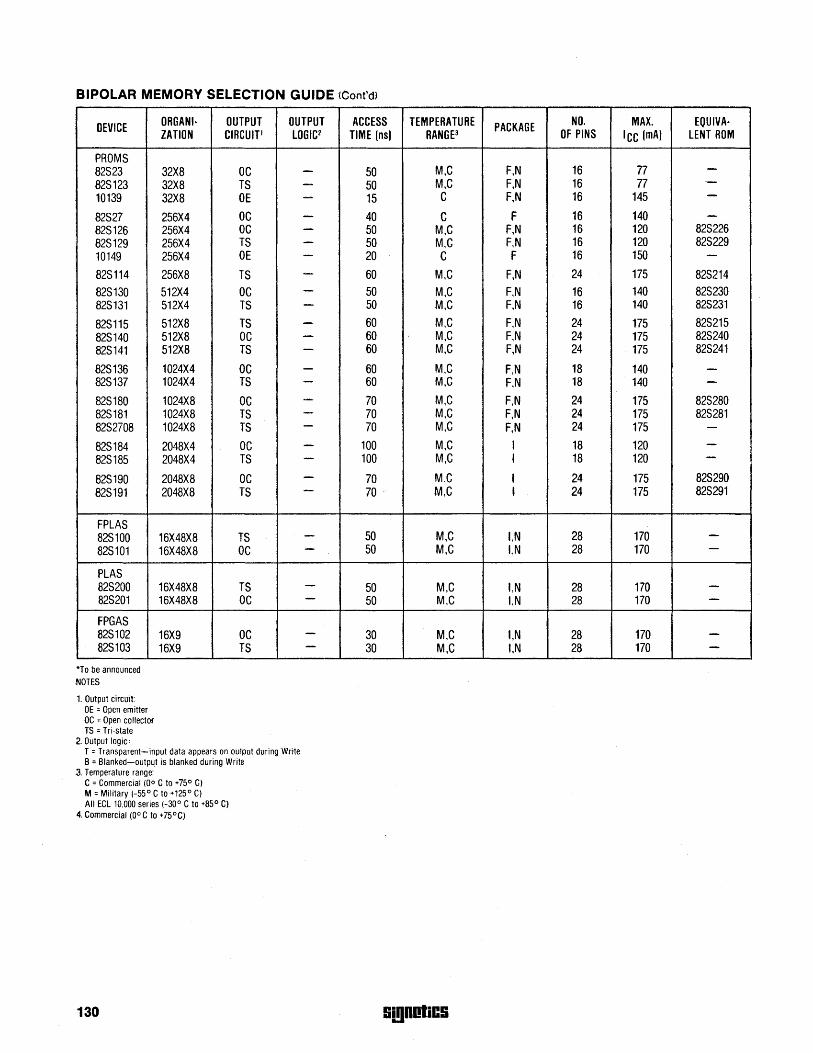
BIPOLAR MEMORY SELECTION GUIDE {Cont'dJ
DEVICE
PROMS 82S23 82S123 10139 82S27 82S126 82S129 10149 82S114 82S130 82S131 828115 82S140 82S141 82S136 82S137 82S180 82S181 82S2708 82S184 828185
82S190 82S191
FPLAS 82S100 82S101
PLAS 82S200 82S201
FPGAS 82S102 82S103
·To be announced NOTES
1. Output circuit: OE = Open emitter OC = Open collector TS = Tri-state
2. Output logic:
ORGANI· ZATION
32X8 32X8 32X8 256X4 256X4 256X4 256X4 256X8 512X4 512X4 512X8 512X8 512X8 1024X4 1024X4 1024X8 1024X8 1024X8 2048X4 2048X4
2048X8 2048X8
16X48X8 16X48X8
16X48X8 16X48X8
16X9 16X9
OUTPUT OUTPUT CIRCUIT' LOGIC2
oe -TS -OE -oe -oe -TS -OE -TS -oe -TS -TS -oe -TS -oe -TS -oe -TS -TS -oe -TS -oe -TS -
TS -oe -
TS -oe -
oe -TS -
T = Transparent-input data appears on output during Write B = Blanked-output is blanked during Write
3. Temperature range:· C = Commercial (00 C to +75° C) M = Military (-55° C to +125° C) All ECl 10.000 series (-30° C to +85° C)
4. Commercial (0° C to +75°C)
130
ACCESS TEMPERATURE TIME (ns) RANGP
50 M,e 50 M,e 15 e
40 e 50 M,e 50 M,e 20 e 60 M,e 50 M,e 50 M,e 60 M,e 60 M,e 60 M,e
60 M,e 60 M,e 70 M,e 70 M,e 70 M,e
100 M,e 100 M,e
70 M.e 70 . M,e
50 M,e 50 M,e
50 M,e 50 M,e
30 M,e 30 M,e
S(gnOliC9
PACKAGE NO. MAX. EQUIVA· OF PINS ICC (rnA) LENT ROM
F,N 16 77 -F,N 16 77 --F,N 16 145 -F 16 140 -
F,N 16 120 82S226 F,N 16 120 82S229 F 16 150 -
F,N 24 175 82S214 F,N 16 140 828230 F,N 16 140 82S231 F,N 24 175 828215 F,N 24 175 82S240 F,N 24 175 82S241
F,N 18 140 -F,N 18 140 -F,N 24 175 828280 F,N 24 175 828281 F,N 24 175 -I 18 120 -I 18 120 -I 24 175 82S290 I 24 175 82S291
f,N 28 170 -t,N 28 170 -
t,N 28 170 -I,N 28 170 -
I,N 28 170 -I,N 28 170 -
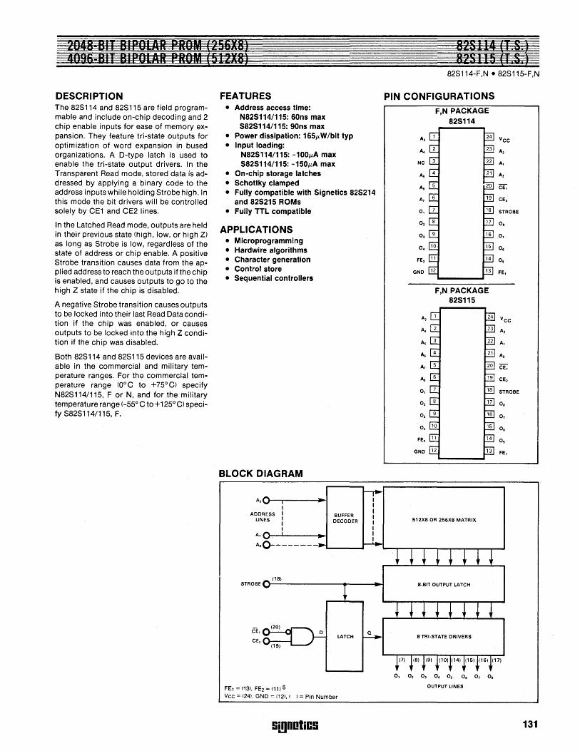
2048 BIT BIPOLAR PROM (256X8) 4096 811 81POLAR PROM (51218)
DESCRIPTION The 82S114 and 82S115 are field programmable and include on-chip decoding and 2 chip enable inputs for ease of memory expansion. They feature tri-state outputs for optimization of word expansion in bused organizations. A D-type latch is used to enable the tri-state output drivers. In the Transparent Read mode, stored data is addressed by applying a binary code to the address inputs while holding Strobe high. In this mode the bit drivers will be controlled solely by CE1 and CE2 lines.
In the Latched Read mode, outputs are held in their previous state (high, low, or high Z) as long as Strobe is low, regardless of the state of address or chip enable. A positive Strobe transition causes data from the applied address to reach the outputs if the chip is enabled, and causes outputs to go to the high Z state if the chip is disabled.
A negative Strobe transition causes outputs to be locked into their last Read Data condition if the chip was enabled, or causes outputs to be locked into the high Z condition if the chip was disabled.
Both 82S114 and 82S115 devices are available in the commercial and military temperature ranges. For the commercial temperature range (aOC to +75°C) specify N82S114/115, F or N, and for the military temperature range (-55° C to +125° C) specify S82S114/115, F.
FEATURES • Address access time:
N825114/115: 60ns max 5825114/115: 90ns max
• Power dissipation: 1651-' W Ibit typ • Input loading:
N825114/115: -100I-'A max 5825114/115: -150I-'A max
• On-Chip storage latches • 5chottky clamped • Fully compatible with 5ignetics 825214
and 825215 ROMs • Fully TTL compatible
APPLICATIONS • Microprogramming • Hardwire algorithms • Character generation • Control store • 5equential controllers
BLOCK DIAGRAM
ADDRESS LINES
A,
(1BI STROBE
CE,
CE2~------'
FE1 = (13), FE2 = (11) 5
BUFFER DECODER
LATCH
vcc = (24), GND = (12), ( ) = Pin Number
Si!lDOliCS
Q
82S114 (T S ) 82S115 (T S )
82S114-F,N.82S115-F,N
PIN CONFIGURATIONS
F,N PACKAGE 825114
NC A,
F,N PACKAGE 825115
512XS OR 256XS MATRIX
S·BIT OUTPUT LATCH
S TRI·STATE DRIVERS
0, O2 0 3 O. O. O. 0, O.
OUTPUT LINES
0,
FE,
131
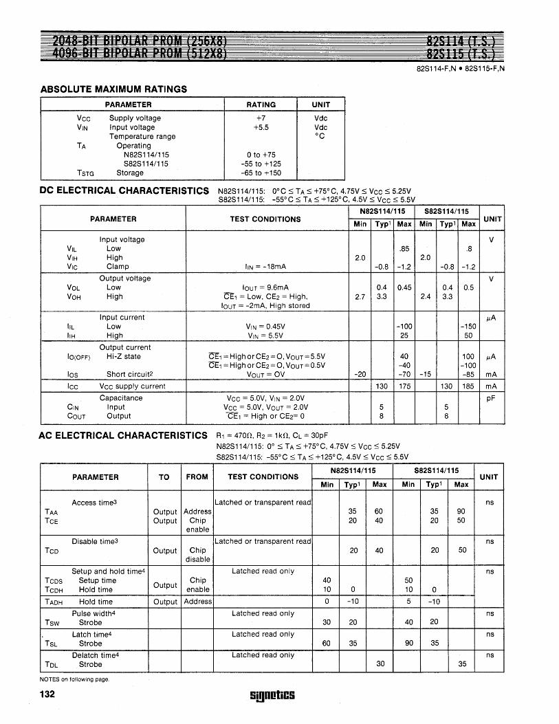
IIIII11 1111[1111111111111 ABSOLUTE MAXIMUM RATINGS
PARAMETER RATING UNIT
Vee Supply voltage +7 Vdc VIN Input voltage +5.5 Vdc
Temperature range °C TA Operating
N828114/115 o to +75 882S114/115 -55 to +125
TSTG Storage -65 to +150
DC ELECTRICAL CHARACTERISTICS N82S114/115: O°C $ TA $ +75°C, 4.75V $ Vee $ 5.25V S82S114/115: -55°C $ TA $ +125°C, 4.5V $ Vee $ 5.5V
N825114/115 PARAMETER TE5T CONDITIONS
Min Typ1 Max
Input voltage VIL Low .85 VIH High 2.0 Vie Clamp liN = -18mA -0.8 -1.2
Output voltage VOL Low lOUT = 9.6mA 0.4 0.45 VOH High CE1 = Low, CE2 = High, 2.7 3.3
lOUT = -2mA, High stored
Input current IlL Low VIN = 0.45V -100 IIH High VIN = 5.5V 25
Output current 10(OFF) Hi-Z state CE1 = High or CE2 = 0, VOUT = 5.5V 40
GE1 = High or CE2 = 0, VOUT = 0.5V -40 los 8hort circuit2 VOUT = OV -20 -70
lee Vee supply current 130 175
CapaCitance Vee = 5.0V, VIN = 2.0V CIN Input Vee = 5.0V, VOUT = 2.0V 5 GOUT Output GE1 = High or GE2= 0 8
AC ELECTRICAL CHARACTERISTICS R1 == 4700, R2 = 1 kO, CL == 30pF
N828114/115: 0° $ TA $ +75°C, 4.75V $ Vee $ 5.25V
882S114/115: -55°C $ TA $ +125°C, 4.5V $ Vee $ 5.5V
5825114/115
Min Typ1 Max
.8 2.0
-0.8 -1.2
0.4 0.5 2.4 3.3
-150 50
100 -100
-15 -85
130 185
5 8
N82S114/115 S825114/115 PARAMETER TO FROM TEST CONDITIONS
Min Typ1 Max Min Typ1 Max
Access time3 Latched or transparent read TAA Output Address 35 60 35 90 TeE Output Chip 20 40 20 50
enable
Disable time3 Latched or transparent read Teo Output Chip 20 40 20 50
disable
Setup and hold time4 Latched read only TeDs Setup time
Output Chip 40 50
TeDH Hold time enable 10 0 10 0
TADH Hold time Output Address 0 -10 5 -10
Pulse width4 Latched read only Tsw Strobe 30 20 40 20
Latch time4 Latched read only TSL Strobe 60 35 90 35
Delatch time4 Latched read only TDL Strobe 30 35
NOTES on following page.
132 Gi!)DntiCG
UNIT
V
V
p.A
p.A
mA
mA
pF
UNIT
ns
ns
ns
ns
ns
ns
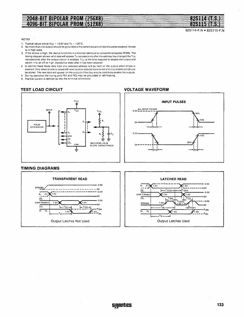
2048 BIT BIPOLAR PROM (,S6X8) 82S114 (I S ) 4096 BIT BIPOLAR PROM (512X8) 825115 (I S )
82S114-F,N .82S115-F,N
NOTES
1. Typical values are at Vcc = +5.0V and TA = +25°C. 2. No more than one output should be grounded at the same time and strobe should be disabled. Strobe
is in high state. 3. If the strobe is high, the device functions in a manner identical to conventional bipolar ROMs. The
timing diagram shows valid data will appear TA nanoseconds after the address has changed the TCE nanoseconds after the output circuit is enabled. TCD is the time required to disable the output and switch it to an off or high impedance state after it has been enabled.
4. In latched Read Mode data from any selected address will be held on the output when strobe is lowered. Only when strobe is raised will new location data be transferred and chip enable conditions be stored. The new data will appear on the outputs if the chip enable conditions enable the outputs.
5. During operation the fusing pins FE1 and FE2 may be grounded or left floating. 6. Positive current is defined as into the terminal referenced.
TEST LOAD CIRCUIT VOLTAGE WAVEFORM
PULSE GENERATOR
VCC
(INCLUDES JIG & SCOPE CAPACITANCE)
-=
TIMING DIAGRAMS
TRANSPARENT READ
, ·3.0V STROBE,'
---'----------------- ---- -·OV ,,~~---- ----- - --- - ------ --'3.0V
'---------------------------OV
C_E_,_~--.... ,,-----_,,----.3.0V
-----OV eE,
0,.
Output Latches Not Used
Gi!)OOtiCG
INPUT PULSES
ALL INPUT PULSES .'::----ji,-----------,,!t% -30V ~ {[10%
90% OV--------
.-.... 50S ...-- --...... 5ns
LATCHED READ ,/""------·3.0V
_---+--~ ,r--------·3.0V
---+--" "~---+-~ I '------OV
Output Latches Used
133
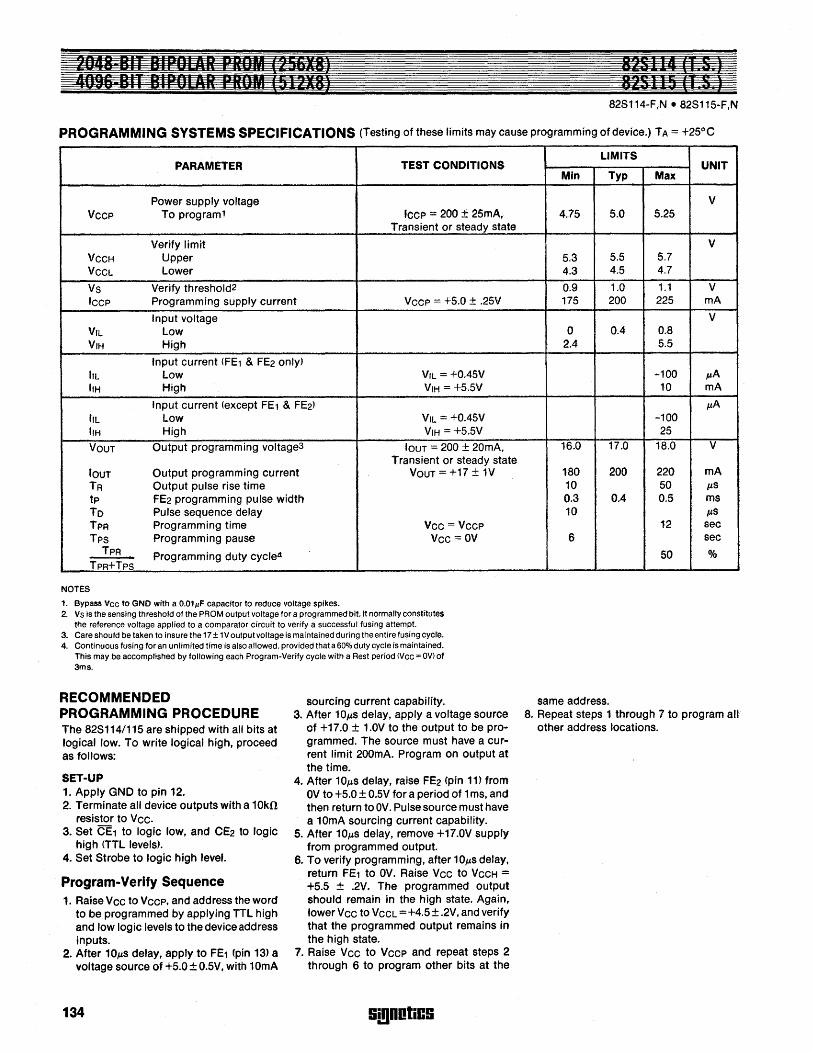
2048 BIT BIPOLAR PROM (256X8) 82S114 (T S ) 4096 BII BIPOLAR PROM (51218) 82S115 (1.S J
828114-F,N·828115-F,N
PROGRAMMING SYSTEMS SPECIFICATIONS (Testing of these limits may cause programming of device.) TA = +250 C
PARAMETER TEST CONDITIONS
Power supply voltage Vecp To programl Iccp = 200 ± 25mA,
Transient or steady state
Verify limit VCCH Upper VCCL Lower
Vs Verify threshold2 Iccp Programming supply current Vccp = +5.0 ± .25V
Input voltage V,L Low V,H High
Input current (FEl & FE2 only) IrL Low VrL = +0.45V IrH High VrH = +5,5V
Input current (except FEl & FE2) IrL Low VrL = +0.45V IIH High VrH = +5,5V
VOUT Output programming voltage3 lOUT = 200 ± 20mA, Transient or steady state
lOUT Output programming current VOUT = +17 ± 1V TR Output pulse rise time tp FE2 programming pulse width To Pulse sequence delay TPR Programming time Vcc = Vccp Tps Programming pause Vcc = OV
TPR Programming duty cycle4
TPR+Tps
NOTES
1. Bypass Vee to GND with a 0.01 fJ.F capacitor to reduce vortage spikes. 2. Vs is the senSing threshold of the PROM output voltage for a programmed bit. It normally constitutes
the reference voltage applied to a comparator circuit to verify a successful fusing attempt. 3. Care should be taken to insure the 17 ± 1 Voutput voltage is maintained during the entire fUSing cycfe. 4. Continuous fUSing for an unlimited time is also allowed, provided that a 60% duty cycle is maintained.
This may be accomplished by following each Program-Verify cycle with a Rest period (Vee = OV~ of 3ms.
RECOMMENDED PROGRAMMING PROCEDURE The 828114/115 are shipped with all bits at logical low. To write logical high, proceed as follows:
SET-UP 1. Apply GND to pin 12. 2. Terminate all device outputs with a 10kO
resistor to Vcc. 3. Set eEl to logiC low, and CE2 to logic
high (TTL levels). . 4. Set Strobe to logiC high 'evel.
Program-Verify Sequence 1. Raise Vcc to Vccp, and address the word
to be programmed by applying TTL high and low logic levels to the device address inputs.
2. After 10p.s de fay, appfy to FE1 (pin 13) a voltage source of +5.0 ± 0.5V, with 10mA
134
sourcing current capability. 3. After 10p.s delay, apply a voltage source
of +17.0 ± 1.0V to the output to be programmed. The source must have a cur .. rent limit 200mA. Program on output at the time.
4. After 10p.s delay, raise FE2 (pin 11) from OV to +5.0 ± 0.5V for a period of 1 ms, and then retu rn to OV. Pu Ise sou rce must have a 10mA sourcing current capability.
5. After 10p.s delay, remove +17.0V supply from programmed output.
6. To verify programming, after 10p.s delay, return FEl to OV. Raise Vcc to VCCH = +5.5 ± .2V. The programmed output should remain in the high state. Again, 'ower Vcc to VCCL =+4.5± .2V, and verify that the programmed output remains in the high state.
7. Raise Vcc to Vccp and repeat steps 2 through 6 to program other bits at the
lijgnoticli
LIMITS UNIT
Min Typ Max
V 4.75 5.0 5.25
V 5.3 5.5 5.7 4.3 4.5 4.7
0.9 1.0 1.1 V 175 200 225 rnA
V 0 0.4 0.8
2.4 5.5
-100 ",A 10 rnA
p.A -100 25
16.0 17.0 18.0 V
180 200 220 mA 10 50 P.s 0.3 0.4 0.5 ms 10 p.s
12 sec 6 sec
50 %
same address. 8. Repeat steps 1 through 7 to program aU
other address locations.
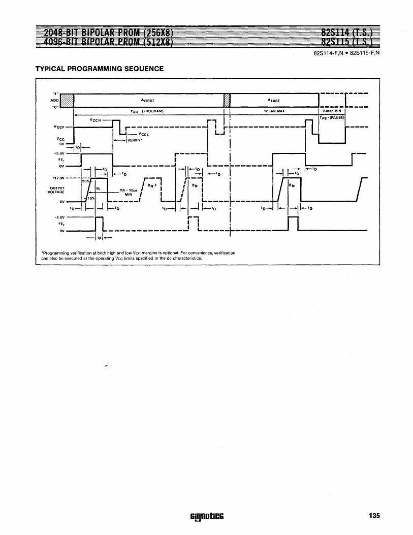
2048 BIT BIPOLAR PROM (25618) 825114 (T S ) 4096 811 BIPOLAR PROM (51218) 825115 (F.5.)
82S114-F,N .82S115-F,N
TYPICAL PROGRAMMING SEQUENCE
n1np~~ ______________________________________ ~~ ______________________ ~
~:~~ A LAST
TpR - (PROGRAM) 12.Osec MAX
r=uVCCH ., , fLLjTPS-(PAUSE)
VCCP- ~r-:c:-----------' Lst------------- ----V~; I VERIFY. 'I
-ltOl- ,
+5~:: -r--l r-----' I I r--ov --1_
1
- 1-'to L-I _______ ..J -II-to I r----I' ______ J -l -I I-~to-----· I -I J-tO II - I-tO I_to I
~17.OV ---- 90% ,---, r-' )' I BN" I I eN I
V~~;~! TI'I "10/JS I I I I MIN I I I I '
OV ____ ~ L_ J L ____ ~-------
to- I- -1 I-to to_ I- -1 I-to t to I-. -j I_to -5.0V f1 r-- I n F:; ______ --i _____________ J L ____ + _______ ---.J 1 ___________ _
-ltpl-'Programming verification at both high and low Vee margins is optional. For convenience, verification can also be executed at the operating Vee -limits specified in the dc characteristics.
Ii!!lDOliCG 135
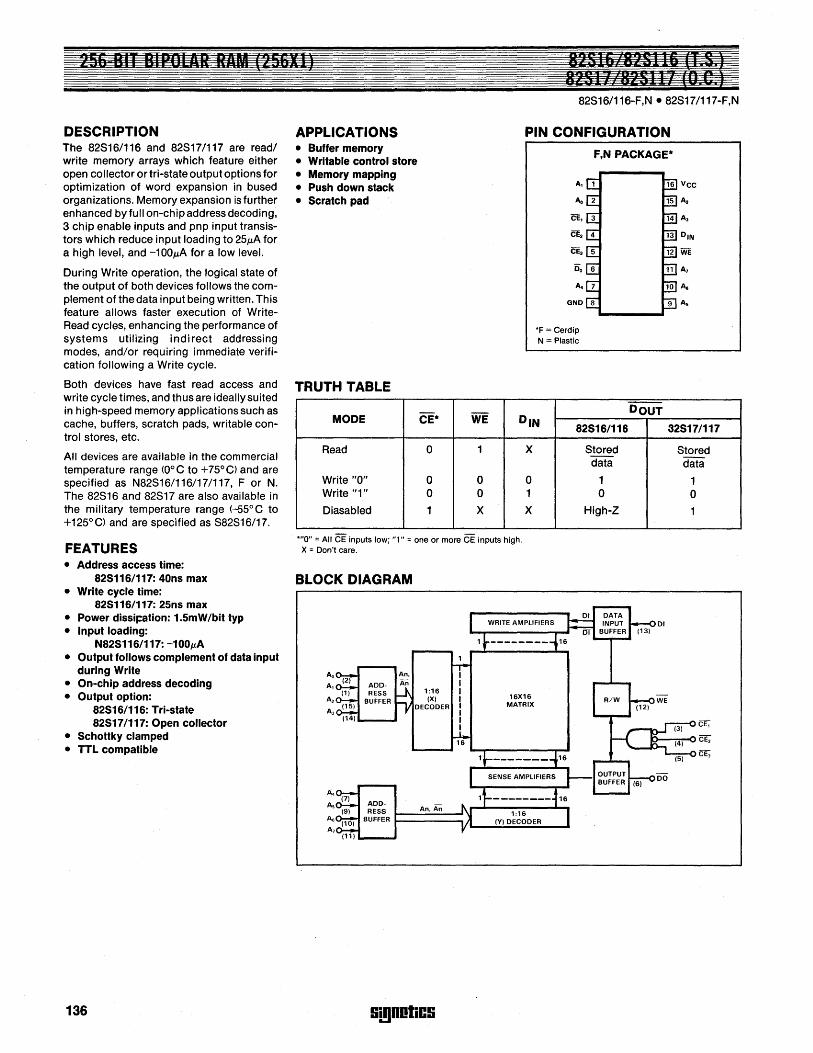
256 BIT BIPOLAR RAM (25611)
DESCRIPTION The 82816/116 and 82817/117 are readl write memory arrays which feature either open collector or tri-state output options for optimization of word expansion in bused organizations. Memory expansion is further enhanced by full on-chip address decoding, 3 chip enable inputs and pnp input transis-tors which reduce input loading to 25f.lA for a high level, and -100f.lA for a low level.
During Write operation, the logical state of the output of both devices follows the com-plement of the data input being written. This feature allows faster execution of Write-Read cycles, enhancing the performance of systems utilizing indirect addressing modes, and/or requiring immediate verifi-cation following a Write cycle.
APPLICATIONS • Buffer memory • Writable control store • Memory mapping • Push down stack • Scratch pad
Both devices have fast read access and TRUTH TABLE write cycle times, and thus are ideally suited in high-speed memory applications such as cache, buffers, scratch pads, writable control stores, etc.
All devices are available in the commercial temperature range (DOC to +75° C) and are specified as N82816/116/17/117, F or N. The 82816 and 82817 are also available in the military temperature range (-55°C to +125°C) and are specified as 882S16/17.
MODE
Read
Write "0" Write "1"
Diasabled
CE* WE
0 1
0 0 0 0
1 X
82S16 82$116 (T S ) 82511 825117 (0 C )
82816/116-F,N .82817/117-F,N
PIN CONFIGURATION
F,N PACKAGE*
'F = Cerdip N = Plastic
DIN 82S16/116
X 8tored data
0 1 1 0
X High-Z
DOUT
32S17/117
8tored data
1 0
1
FEATURES '''0'' = All CE inputs low; "1" = one or more CE inputs high.
• Address access time: 82S116/117: 40ns max
• Write cycle time: 82S116/117: 25ns max
• Power dissir:ation: 1.5mW/bit typ • Input loading:
N82S116/117: -100f.lA • Output follows complement of data input
during Write • On-chip address decoding • Output option:
82S 16/116: Tri-state 82S17/117: Open collector
• Schottky clamped • TTL compatible
136
X = Don't care.
BLOCK DIAGRAM
Ao
A,
A2 WE
A3
eE,
CE2
cEo
DO
A.
As An. Ali A6
A,
Si!lDOliCS
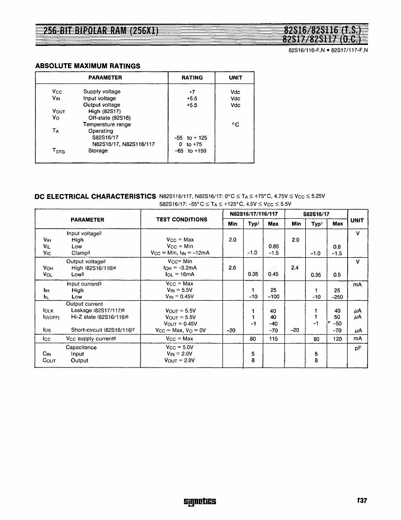
256 BIT BIPOLAR RAM (25611)
82816/116-F,N·82817/117-F,N
ABSOLUTE MAXIMUM RATINGS
PARAMETER RATING UNIT
Vee 8upply voltage +7 Vdc VIN Input voltage +5.5 Vdc
Output voltage +5.5 Vdc VOUT High (82817) Vo Off-state (82816)
Temperature range °C TA Operating
882816/17 -55 to + 125 N828 16/17, N828116/117 o to +75
TSTG 8torage -65 to +150
DC ELECTRICAL CHARACTERISTICS N828116/117, N82816/17: O°C:::; TA:::; +75°C, 4.75V:::; Vee:::; 5.25V
882816/17: -55°C:::; TA:::; +125°C, 4.5V:::; Vee:::; 5.5V
N82S16/17/116/117 S82S16/17 PARAMETER TEST CONDITIONS
Min Typ1 Max Min Typ1
Input voltage2
VIH High Vee = Max 2.0 2.0 VIL Low Vee = Min 0.85 Vie Clamp3 Vee = Min, liN = -12mA -1.0 -1.5 -1.0
Output voltage2 Vee= Min VOH High (82816/116)4 10H = -3.2mA 2.6 2.4 VOL LowS 10l = 16mA 0.35 0.45 0.35
Input current3 Vee - Max ItH High VIN = 5.5V 1 25 1 IlL Low VIN = 0.45V -10 -100 -10
Output current 10LK Leakage (82817/117)6 VOUT = 5.5V 1 40 1 10(OFF) Hi-Z state (82816/116)6 VOUT = 5.5V 1 40 1
VOUT = 0.45V -1 -40 -1 ...,.
los 8hort-circuit (82816/116)7 Vee = Max, Vo = OV -20 -70 -20
lee Vee supply current8 Vee = Max 80 115 80
CapaCitance Vee = 5.0V CIN Input VIN = 2.0V 5 5 COUT Output VOUT = 2.0V 8 8
Si!lDOliCS
Max UNIT
V
0.8 -1.5
V
0.5
rnA 25
-250
40 f.1A 50 f.1A -50 -70 f.1A
120 rnA
pF
f37
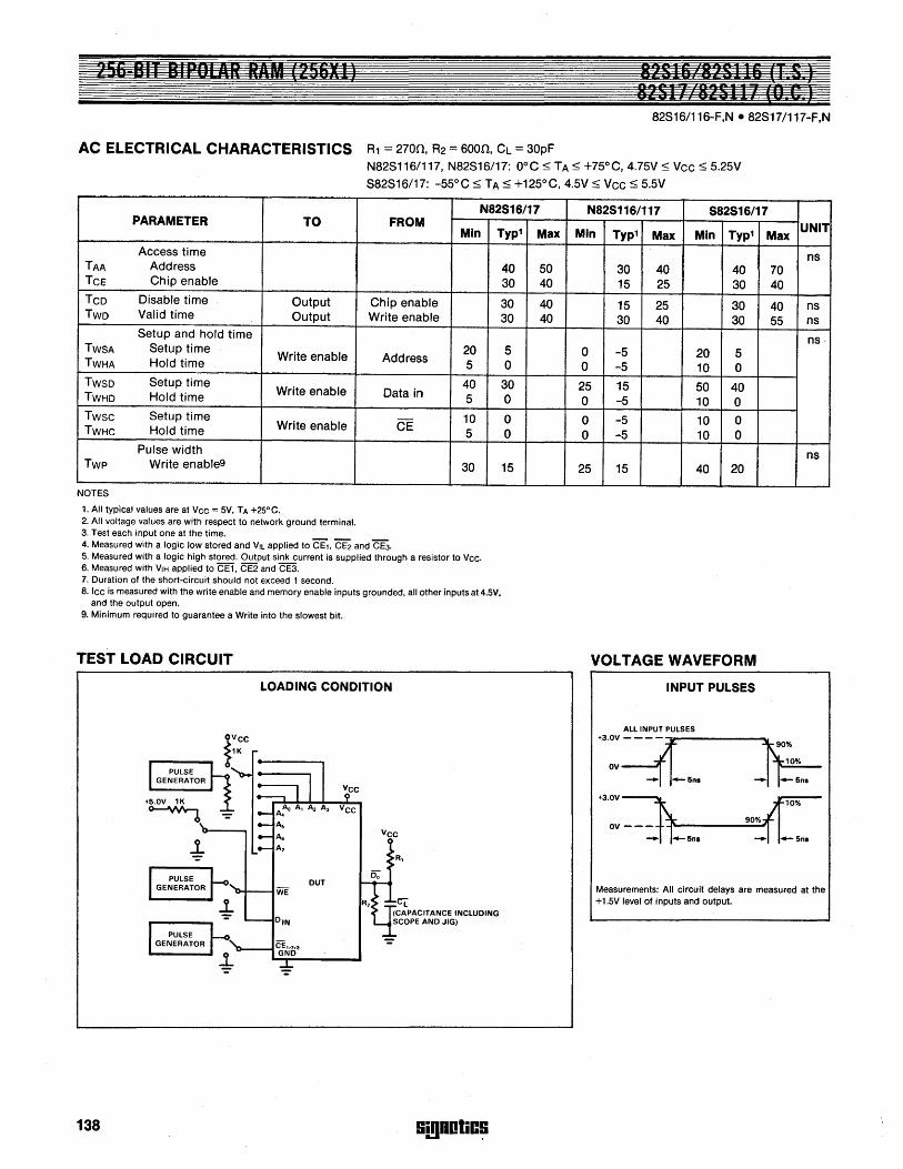
256 BIT BI,O[I\R RAM (25611) 82S16 828116 (T 8 ) 82517 825111 (0 C )
82S16/116-F,N .82S17/117-F,N
AC ELECTRICAL CHARACTERISTICS Rl = 2700, R2 = 600n, CL = 30pF
N82S116/117, N82S16/17: O°C -::; TA -::; +75°C, 4.75V -::; Vcc -::; 5.25V
882S16/17: -55°C -::; TA -::; +125°C, 4.5V -::; VCC -::; 5.5V
N82S16/17 PARAMETER TO FROM
Min Typ1
Access time TAA Address TCE Chip enable
TCD Disable time Output Chip enable TWD Valid time Output Write enable
Setup and hold time TWSA Setup time
Write enable Address 20
TWHA Hold time 5
TWSD Setup time Write enable Data in
40 TWHD Hold time 5
Twsc 8etup time Write enable CE
10 TWHC Hold time 5
Pulse width Twp Write enable9 30
NOTES 1. All typical values are at Vee = 5V, TA +25°C. 2. All voltage values are with respect to network ground terminal. 3. Test each input one at the time. 4. Measured with a logic low stored and VIL applied to CE1, CE2 and C'E3. 5. Measured with a logic high stored. Output sink current is supplied through a resistor to Vee. 6. Measured with VIH applied to CE1, CE2 and CE3. 7. Duration of the short-circuit should not exceed 1 second. 8. Icc is measured with the write enable and memory enable inputs grounded, all other inputs at 4.5V.
and the output open. 9. Minimum required to guarantee a Write into the slowest bit.
TEST LOAD CIRCUIT
LOADING CONDITION
Vee
138
R,
CL (CAPACITANCE INCLUDING SCOPE AND JIG)
!ii!lnllliC~
40 30
30 30
5 0
30 0
0 0
15
Max
50 40
40 40
N82S116/117 S82S16/17
Min Typ1 Max Min Typ1 Max UNIT
ns 30 40 40 70 15 25 30 40
15 25 30 40 ns 30 40 30 55 ns
ns, 0 -5 20 5 0 -5 10 0
25 15 50 40 0 -5 10 0
0 -5 10 0 0 -5 10 0
ns 25 15 40 20
VOLTAGE WAVEFORM
INPUT PULSES
All INPUT PULSES +3.0V - - - - "..----___
OV 10%
+3.0V 10%
90%
Measurements: All circuit delays are measured at the +1.5V level of inputs and output.
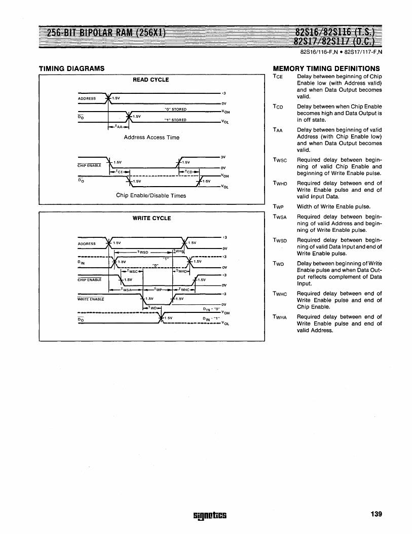
256 BIT BIPOLAR HAM (25611)
TIMING DIAGRAMS
READ CYCLE
------~ r-------------------------------+3 ADDRESS ~ (.1 SV ------) \.,--' -----------------------------oV ________ +-__ ~ r-________ "_O"_S_TO.R.ED __________
VOH
DO ________ +-___ ~ ________ "_1'_'S_TO_R_E_D __________ VOl 1,SV
_TAA
Address Access Time
t'v t'v:: ____ ~_TC_E-::I-----_____________ ~:~~-~ VO
H
DO ~1~V ~1~V ~----------------'~-----VOL
CHIP ENABLE
Chip Enable/Disable Times
WRITE CYCLE
+3
ADDRESS 1.SV
OV TWSD TWH~
"1" 1.SV
OV
+3 CHIP ENABLE 1.SV
'--__ ~ ______ --~---J+-______ OV
r---......:------- +3 WRITE ENABLE
~-----'---------------OV
TWD1
DIN = "0"
---------------.. -----~ VOH
00 ~ 1 SV DIN = "1" _______________________ .J - -------____ VOL
!ii!lDOliC!i
lIe"aE 82S16/116-F,N .82S17/117-F,N
MEMORY TIMING DEFINITIONS TCE
TCD
Twsc
TWHD
Twp
TWSA
TWSD
TWD
Delay between beginning of Chip Enable low (with Address valid) and when Data Output becomes valid.
Delay between when Chip Enable becomes high and Data Output is in off state.
Delay between beginning of valid Address (with Chip Enable low) and when Data Output becomes valid.
Required delay between beginning of valid Chip Enable and beginning of Write Enable pulse.
Required delay between end of Write Enable pulse and end of valid Input Data.
Width of Write Enable pulse.
Required delay between beginning of valid Address and begin-ning of Write Enable pulse.
Required delay between beginning of valid Data Inputand end of Write Enable pulse.
Delay between beginning of Write Enable pulse and when Data Output reflects complement of Data Input.
TWHC Required delay between end of Write Enable pulse and end of Chip Enable.
TWHA Required delay between end of Write Enable pulse and end of val id Add ress.
139

140 9i!100liC9

APPEnDIX
GillDOliC!i 141

142 lii!lDOliCIi
81300 DESIGNER'S EVALUATION KIT INSTRUCTION MANUJ\L 81300 KI100 5K
DESCRIPTION The Signetics 8X300 Fixed Instruction Bipolar Microprocessor is a high performance microprocessor optimized for control and data movement appl ications.
The unique features of the 8X300 IV bus and instruction set permit 8-bit parallel data to be rotated or masked before undergoing arithmetic or logical operations. Then, the data may be shifted and merged into any field of from 1 to 8 contiguous bits at the destination. The entire process of input, shifting, processing and output is accomplished in one instruction cycle time. The 250ns cycle time makes the 8X300 suited for high speed applications.
The evaluation board contains all the elements which a designer needs to familiarize ·himself with the 8X300 for his systems applications. Included with the 8X300 are 4 1/0 ports for external device interface, 256 bytes of temporary (working) data storage and 512 words of program storage, all properly
DEVICE MFG
U14 Signetics U2-U9 U15-16 U13, U21, U26, U27 U1 U10-U11 U17-U20 U23, U25 U12 U22, U24 Signetics 01 02 RN1-RN3 Dale R1, R3, R4 R5 R2 C2-C20, C22-C30 Ct, C21 Zl J104 Berg J101 Berg J105 Berg
connected to the 8X300 to allow immediate exercising of the board. For this purpose, the PROMs are preprogrammed with the 1/0 control, RAM control and RAM integrity diagnostic programs. With the remaining PROM space, the designer may enter his own benchmark, test or development routines.
The board design allows complete flexibility 1n access to the address, instruction and IV busses as well as all controls and signals of the 8X300. The IV bus, I/O port user connection, clock Signals, control lines, address bus and instruction bus are wired to output pins, the board edge connector and flat cable connectors.
The board layout permits variations andlor expansion of the basic design. In addition to the access to all signals for transfer off the board, a wire wrap area is provided so that the designer may add to the board circuitry as he desires. The addition may include memory, additional interfaces, or special circuits which meet specific user requirements.
PART NUMBER
N8X3001 N82S116B N82S1151 N8T32N N8T31N N8T26AB N74LS157B N74LS74A N74LS27A N74LSOOA 2N5320 2N2222 CSP-10E-01-102-K 1k!l1/4W 4k!l 1/4W 8k!l 1/4W 0.1J1F 22J1F 8.00 MHz 65616-134 65616-150 65616-120
Robinson-Nugent ICN-163-53 Robinson-Nugent ·'CN-246-54 Robinson-Nugent SB-25
81,S2 Amp 435640-5 S5,S6 Alco MSTS-104D 83,S4 Digitast ST
Smith 230 (red) Smith 230 (black) 8AE CPH 8100-100
Table 1 KIT CONTENTS
GillDOliC!i
Controls are also provided for diagnostic and instructional purposes by allowing various operating modes. In the WAIT mode, the program may be single stepped for ease of checkout. The one-shot instruction jamming allows control of the program start location, changes of program flow, changing or examining the internal registers, or testing of simple sequences. The repeated instruction jamming provides a means of repetitive execution of an instruction so that the 1/0 bus and the control lines may be examined without software changes. In both of these jam cases, the jammed instruction is selected by board-mounted switches.
Auxiliary Circuits The 8X300 can be used with any bipolar (or TTL-compatible) ICs. It can directly address 8192 program instruction locations and up to 512 1/0 ports. Memory paging may be employed for larger working storage. Typical auxiliary circuits include:
DESCRIPTION QTY
Microprocessor 1 RAM (256X1) 8 PROM (512X8) 2 110 Port (Tri-state) 4 Latch 1 Transceiver 2 Multiplexer 4 Flip-Flop 2 NOR Gate 1 NAND Gate 2 Transistor 1 Transistor 1 Resistor network 3 Resistor 3 Resistor 1 Resistor 1 Capacitor 29 Capacitor 2 Crystal 1 Connector 1 Connector 1 Connector 4 Socket 2 Socket 7 Strip socket 2 Dip switch 2 Toggle switch 2 Momentary switch 2 Binding post 1 Binding post 1 50/100 edge connector 1 PC board 1 Packing case 1 Assembly manual 1
143
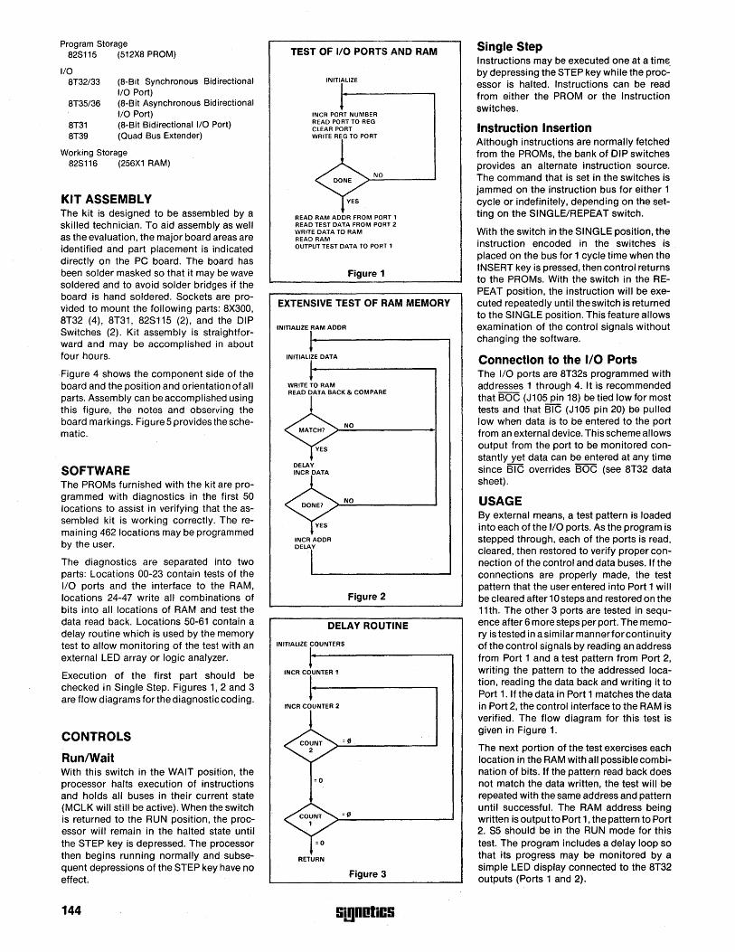
Program Storage 82S115 (512X8 PROM)
1/0 8T32/33 (8-Bit Synchronous Bidirectional
1/0 Port) 8T35/36 (8-Bit Asynchronous Bidirectional
1/0 Port) 8T31 (8-Bit Bidirectional I/O Port) 8T39 (Quad Bus Extender)
Working Storage 82S116 (256X1 RAM)
KIT ASSEMBLY The kit is designed to be assembled bya skilled technician. To aid assembly as well as the evaluation, the major board areas are identified and part placement is ind icated directly on the PC board. The board has been solder masked so that it may be wave soldered and to avoid solder bridges if the board is hand soldered. Sockets are provided to mount the following parts: 8X300, 8T32 (4), 8T31 , 82S115 (2), and the DIP SwHches (2). Kit assembly is straightforward and may be accomplished in about four hours.
,Figure 4 shows the component side of the board and the position and orientation of all parts. Assembly can be accomplished using this figure, the notes and observing the board markings. Figure 5 provides the schematic.
SOFTWARE The PROMs furnished with the kit are programmed with diagnostics in the first 50 locations to assist in verifying that the assembled kit is working correctly. The remaining 462 locations may be programmed by the user.
The diagnostics are separated into two parts: Locations 00-23 contain tests of the I/O ports and the interface to the RAM, locations 24-47 write all combinations of bits into all locations of RAM and test the data read back. Locations 50-61 contain a delay routine which is used by the memory test to allow monitoring of the test with an external LED array or logic analyzer.
Execution of the first part should be checked in Single Step. Figures 1,2 and 3 are flow diagrams forthe diagnostic coding.
CONTROLS
Run/Wait With this switch in the WAIT position, the processor halts execution of instructions and holds all buses in their current state (MCLK will still be active). When the switch is returned to the RUN position, the processor will remain in the halted state until the STEP key is depressed. The processor then begins running normally and subsequent depressions of the STEP key have no effect.
144
TEST OF 1/0 PORTS AND RAM
INITIALIZE
INCR PORT NUMBER READ PORT TO REG CLEAR PORT WRITE REG TO PORT
NO
READ RAM AD DR FROM PORT 1 READ TEST DATA FROM PORT 2 WRITE DATA TO RAM READ RAM OUTPUT TEST DATA TO PORT 1
Figure 1
EXTENSIVE TEST OF RAM MEMORY
INITIALIZE RAM ADDR
INITIALIZE DATA
WRITE TO RAM READ lATA BACK & COMPARE
DELAY INCR DATA
INCR AD DR DELAY
NO
NO
Figure 2
DELAY ROUTINE
INITIALIZE COUNTERS
INCR COUNTER 2
RETURN
Figure 3
sagnoliC!i
Single Step Instructions may be executed one at a time, by depressing the STEP key while the processor is halted. Instructions can be read from either the PROM or the Instruction switches.
Instruction Insertion Although instructions are normally fetched from the PROMs, the bank of DIP switches provides an alternate instruction source. The command that is set in the switches is jammed on the instruction bus for either 1 cycle or indefinitely, depending on the setting on the SINGLE/REPEAT switch.
With the switch in the SINGLE position, the instruction encoded in the switches is placed on the bus for 1 cycle time when the INSERT key is pressed, then control returns to the PROMs. With the switch in the REPEAT position, the instruction will be executed repeatedly until the switch is returned to the SINGLE position. This feature allows examination of the control signals without changing the software.
Connection to the I/O Ports The I/O ports are 8T32s programmed with addresses 1 through 4. It is recommended that BOC (J105 pin 18) be tied lowformost tests and that BIC (J105 pin 20) be pulled low when data is to be entered to the port from an external device. This scheme allows output from the port to be monitored constantly yet data can be entered at any time since BIC overrides BOC (see 8T32 data Sheet).
USAGE By external means, a test pattern is loaded into each of the I/O ports. As the program is stepped through, each of the ports is read, cleared, then restored to verify proper connection of the control and data buses. If the connections are properly made, the test pattern that the user entered into Port 1 will be cleared after 10 steps and restored on the 11th. The other 3 ports are tested in sequence after 6 more steps per port. The memory is tested in a similar manner for continuity of the control signals by reading an address from Port 1 and a test pattern from Port 2, writing the pattern to the addressed location, reading the data back and writing it to Port 1. If the data in Port 1 matches the data in Port 2, the control interface to the RAM is verified. The flow diagram for this test is given in Figure 1.
The next portion of the test exercises each location in the RAM with all possible combination of bits. If the pattern read back does not match the data written, the test will be repeated with the same address and pattern until successful. The RAM address being written is output to Port 1, the pattern to Port 2. S5 should be in the RUN mode for this test. The program includes a delay loop so that its progress may be monitored by a simple LED display connected to the 8T32 outputs (Ports 1 and 2).
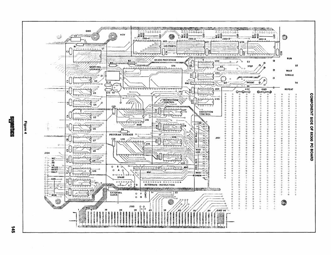
III E5 II a n III
o o o o o o o o
" o o o o o
J10l 0
o {)
o ()
o o <;)
o o o o o o o .:> o o
o o o
o ()
o o
o o o o
o
o o o o
o o o
o
o o ;)
o o o
o o Q
o o o {)
o o o o
.)
o o
o o o o o o o o o
o o o
o
o o o
o
o o o
o
c
o o o o o o o o o o
Q
o o ()
o
o o o
RUN
!!J WAIT
<)
o o o o
o
o o o c
o o
o o o o o o o o
o o o
<)
o o o o o o
o o
o o
SINGLE
REPEAT
(,
o o o o o
(>
o o o o
o o o o
55
56
o
c o o o
o o o o o o
o o o o o o o o o o c o o
o
o C o
Q
o o o
(') o ~ "'U o Z m Z -t o 6 m o "TI ex» >< w C) C)
"'0 (')
CD o ~ :JJ C
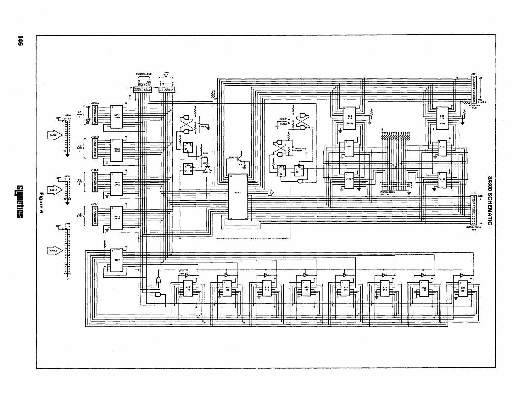
CONTROlBUa DAY ... BUS
1 LIS
j ~ ~
~~~~~~i i----; J104 ~:=~~~:!~::~ J'04
oSSg:g8~~
06 MSB 8K
Ii~-' ~'-I ~U AOORESS
J105,4 J L- BUS
LS.7._~
~ ~' f== ! gi~ ~ ==- -==== .2. -== 82.
r;::::= ". f 1~== Bm ~ r---- ". i--- .-.= ILSB, ~ ~
.B 1:~ ·0004
-:;" SINGLE r;::;::: IM'B, ~ ~ ce~1 -r;F F= IfL--~ I~L....--1*10...-10=- -_ ....
J,:g;" ~J 1 1 g~~,
7474
r~ ~74157 r- I--R74157 g:r=== o Q
f-
~~r-~~ [ 8T32 ep
INSERT
II ~r- l-e.
RUN ~ I-liF ,000,
I L.!!!I~ WAit IC!J ~L--J= 7474
.K o.l~ 7474
~~ ~ o (j o Q
~ 11 ~r- Ir l1 J~2 ~J ep Q 2N2222 cp CP
Cl 8~ p= 1 50 1
I t:===I 741,.7 E t=:: II <-'= t=- 1=t==t'1
g~ I - ~r 1~ I ....= \" ~11 ltmummH~
.: ~ 1:1
I ~ INSTRUCTION
~' Llli ~ 8X3OO SWITCH -
MIS f-'
"I 1.,f'L....--1-
28 L-------
30 31 33 3. 3.
J~' r--J r--
37 3'
02~'
[fc- 40 iiF=== 42 43 4"
,21 ST'2 25
4S 1i I ·0001
~ ..!!. LSS II tNST:~~TION ~~~F=
110 { ..1104 PORT
""1" .. ,; · i?
~ i .. { • PORT
18; 3
~ 8>1' ~l ~{ is- 18 20
C
: . ~{ J101
Q:Y 1 2
L..,!, •
;--r! r;::== g 1T31 r;:=
I ~~l=t-- J. J. J. J. ~ ..L J. lJ ~r::~.l
~ ~ Jt ~ ~ p-~ ~ l 1 I--
l 1 r- 1 r- 1 f--
l 1 f- 1 ~
82' I-- .2. I-- 82S f-'2' ~ 82. >===; 82S I-- .2. F ~~: "6 "0 "0 "6 "6 "6 "6
I~ T~ I~~I ":' .
'--
00 >< Co) o o en o :::t m :iii: ~ o
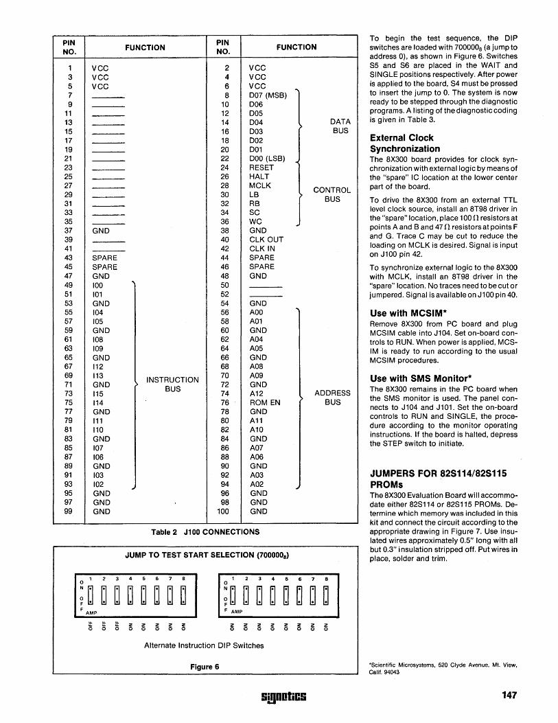
PIN NO.
1 VCC 3 VCC 5 VCC 7 9
11 13 15 17 19 21 23 25 27 29 31 33 35 37 GND 39 41 43 SPARE 45 SPARE 47 GND 49 100 51 101 53 GND 55 104 57 105 59 GND 61 108 63 109 65 GND 67 112 69 113 71 GND 73 115 75 114 77 GND 79 111 81 110 83 GND 85 107 87 106 89 GND 91 103 93 102 95 GND 97 GND 99 GND
0 2 3
: 0 F • 0 0 F
AMP
... ... ... ... 0 ... 0 0
FUNCTION PIN
FUNCTION NO.
2 VCC 4 VCC 6 VCC ... 8 007 (MSB)
10 006 12 DOS 14 004 >
DATA 16 003 BUS 18 002 20 001 22 000 (LSB) .. 24 RESET 26 HALT 28 MCLK
CONTROL 30 LB > BUS 32 RB 34 SC 36 WC
'" 38 GND 40 CLK OUT 42 CLKIN 44 SPARE 46 SPARE 48 GND
"\ 50 52 54 GND 56 AOO "\
58 A01 60 GND 62 A04 64 A05 66 GND 68 A08
INSTRUCTION 70 A09 >
BUS 72 GND 74 A12 ADDRESS 76 ROM EN > BUS 78 GND 80 A11 82 A10 84 GND 86 A07 88 A06 90 GND 92 A03 94 A02 .. .. 96 GND 98 GND
100 GND
Table 2 J100 CONNECTIONS
JUMP TO TEST START SELECTION (7000008)
4 5 6 7 3 0
4 5 6 7 8
0 0 0 0 0 NO ~ . 0 0 0 0 0 0 0 F AMP
Z Z Z Z Z Z Z Z Z Z Z Z Z 0 0 0 0 0 0 0 0 0 0 0 0 0
Alternate Instruction DIP Switches
Figure 6
!iI!lDotiC!i
To begin the test sequence, the DIP switches are loaded with 7000008 (a jump to address 0), as shown in Figure 6. Switches S5 and S6 are placed in the WAIT and SINGLE positions respectively. After power is applied to the board, S4 must be pressed to insert the jump to O. The system is now ready to be stepped through the diagnostic programs. A listing of the diagnostic coding is given in Table 3.
External Clock Synchronization The 8X300 board provides for clock synchronization with external logic by means of the "spare" IC location at the lower center part of the board.
To drive the 8X300 from an external TTL level clock source, install an 8T98 driver in the "spare" location, place 100 n resistors at points A and Band 47 n resistors at points F and G. Trace C may be cut to reduce the loading on MCLK is desired. Signal is input on J100 pin 42.
To synchronize external logic to the 8X300 with MCLK, install an 8T98 driver in the "spare" location. No traces need to be cut or jumpered. Signal is availableon J100 pin 40.
Use with MCSIM* Remove 8X300 from PC board and plug MCSIM cable into J104. Set on-board controls to RUN. When power is applied, MCS-1M is ready to run according to the usual MCSIM procedures.
Use with SMS Monitor* The 8X300 remains in the PC board when the SMS monitor is used. The panel connects to J104 and J101. Set the on-board controls to RUN and SINGLE, the procedure according to the monitor operating instructions. If the board is halted, depress the STEP switch to initiate.
JUMPERS FOR 825114/825115 PROMs The 8X300 Evaluation Board will accommodate either 82S114 or 82S115 PROMs. Determine which memory was included in this kit and connect the circuit according to the appropriate drawing in Figure 7. Use insulated wires approximately 0.5" long with all but 0.3" insulation stripped off. Put wires in place, solder and trim.
'Scientific Microsystems. 520 Clyde Avenue, Mt. View. Calif. 94043
147
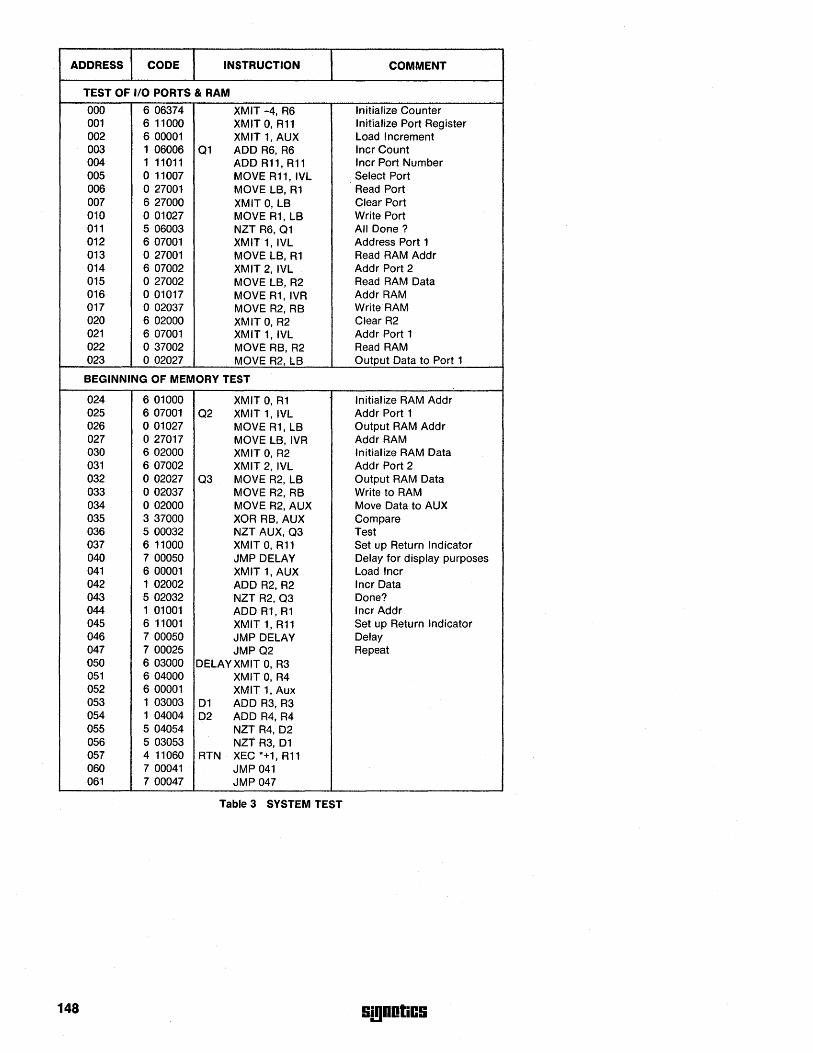
ADDRESS CODE INSTRUCTION COMMENT
TEST OF 1/0 PORTS & RAM
000 6 06374 XMIT -4, R6 Initialize Counter 001 6 11000 XMIT 0, R11 Initialize Port Register 002 6 00001 XMIT 1, AUX Load Increment 003 1 06006 Q1 ADD R6, R6 Incr Count 004 1 11011 ADD R11, R11 Incr Port Number 005 011007 MOVE R11, IVL Select Port 006 o 27001 MOVE LB, R1 Read Port 007 6 27000 XMIT 0, LB Clear Port 010 o 01027 MOVE R1, LB Write Port 011 5 06003 NZT R6, Q1 All Done? 012 6 07001 XMIT 1, IVL Address Port 1 013 o 27001 MOVE LB, R1 Read RAM Addr 014 6 07002 XMIT 2, IVL Addr Port 2 015 o 27002 MOVE LB, R2 Read RAM Data 016 o 01017 MOVE R1, IVR Addr RAM 017 o 02037 MOVE R2, RB Write RAM 020 6 02000 XMIT 0, R2 Clear R2 021 6 07001 XMIT 1, IVL Addr Port 1 022 o 37002 MOVE RB, R2 Read RAM 023 o 02027 MOVE R2, LB Output Data to Port 1
BEGINNING OF MEMORY TEST
024 6 01000 XMIT 0, R1 Initialize RAM Addr 025 6 07001 Q2 XMIT 1, IVL Addr Port 1 026 o 01027 MOVE R1, LB Output RAM Addr 027 o 27017 MOVE LB, IVR Addr RAM 030 6 02000 XMIT 0, R2 Initialize RAM Data 031 6 07002 XMIT 2, IVL Addr Port 2 032 o 02027 03 MOVE R2, LB Output RAM Data 033 o 02037 MOVE R2, RB Write to RAM 034 o 02000 MOVE R2, AUX Move Data to AUX 035 3 37000 XOR RB, AUX Compare 036 5 00032 NZT AUX, Q3 Test 037 6 11000 XMIT 0, R11 Set up Return Indicator 040 7 00050 JMP DELAY Delay for display purposes 041 6 00001 XMIT 1, AUX Load Incr 042 1 02002 ADD R2, R2 Incr Data 043 5 02032 NZT R2, Q3 Done? 044 1 01001 ADD R1, R1 Incr Addr 045 6 11001 XMIT 1, R11 Set up Return Indicator 046 7 00050 JMP DELAY Delay 047 7 00025 JMP 02 Repeat 050 6 03000 DELAY XMIT 0, R3 051 6 04000 XMIT 0, R4 052 6 00001 XMIT 1, Aux 053 1 03003 D1 ADD R3, R3 054 1 04004 02 ADD R4, R4 055 5 04054 NZT R4, 02 056 5 03053 NZT R3, D1 057 4 11060 RTN XEC *+1, R11 060 7 00041 JMP 041 061 7 00047 JMP 047
Table 3 SYSTEM TEST
148 SmDOliCIi
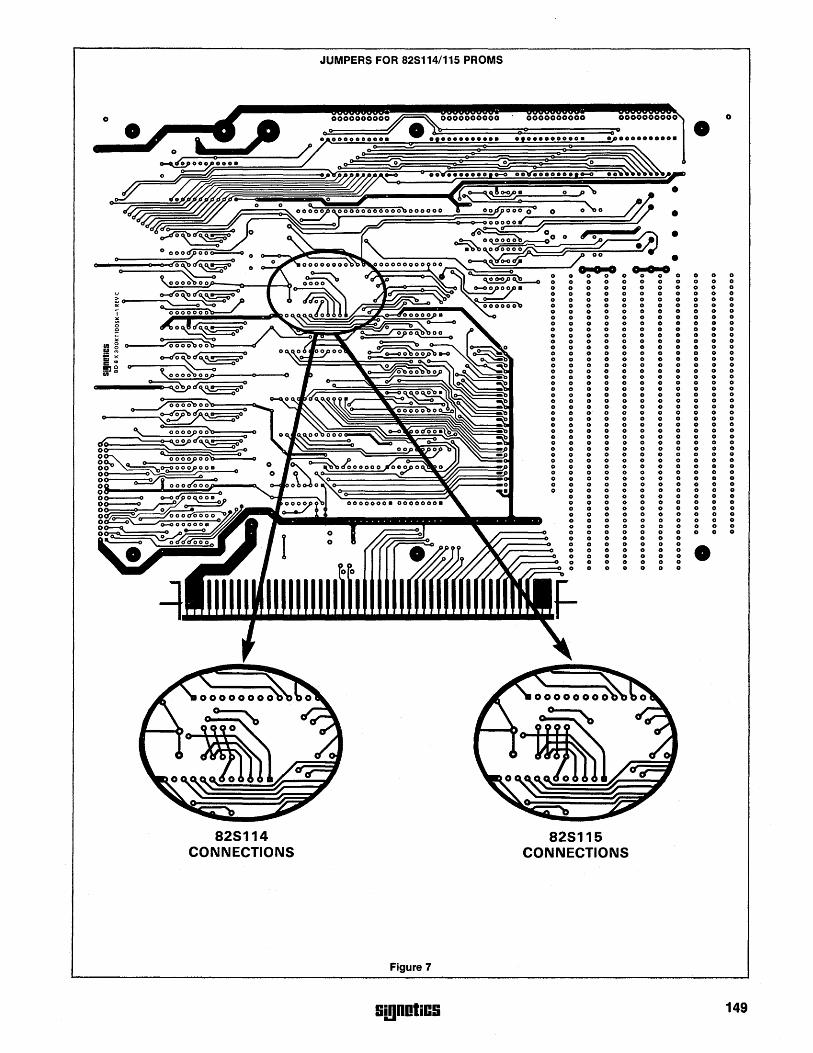
v >
'"
j It.I r:! - )(
IE ~ 0 ~., ~o'¥: 0000
'OOO~OOIJ =- ~d"¥ 00
0
825114 CONNECTIONS
JUMPERS FOR 82S114/115 PROMS
Figure 7
9i!1DOliC9
0 0 0 0 0 0 0 0 0 0 0 0 0 0 0 0 0 0 0 0 0 0 0 0 0 0 0 0 0 0 0 0 0 0 0 0 0 0 0 0 0 0 0 0 0 0 0 0 0 0 0 0 0 0 0 0 0 0 0 0 0 0 0 0 0 0 0 0 0 0 0 0 0 0 0 0 0 0 0 0 0 0 0 0 0 0 0 0 0 0 0 0 0 0 0 0 0 0 0 0 0 0 0 0 0 0 0 0 0 0 0
0 0 0 0 0 0 0 0 0 0 0 0 0 0 0 0 0 0 0 0 0 0 0 0 0 0
825115 CONNECTIONS
o
o
• • •
0 0 0 0 0 0 0 0 0 0 0 0 0 0 0 0 0 0 0 0 0 0 0 0 0 0 0 0 0 0 0 0 0 0 0 0 0 0 0 0 0 0 0 0 0 0 0 0 0 0 0 0 0 0 0 0 0 0 0 0 0 0 0 0 0 0 0 0 0 0 0 0 0 0 0 0 0 0 0 0 0 0 0 0 0 0 0 0 0 0 0 0 0 0 0 0 0 0 0 0 0 0 0 0 0 0 0 0 0 0 0 0 0 0 0 0 0 0 0 0 0 0 0 0 0 0 0 0 0 0 0 0 0 0 0 0 0 0 0 0 0 0 0 0 0 0 0 0 0 0 0 0 0 0 0 0 0 0 0 0 0 0 0 0 0 0 0 0
0 0 0 0 0 0 0 0 0 0 0 0 0 0
0 0 0 0 0 0 0 0 0
149

150 Si!lIOliCS

SAliS ornels
!iagOOliC!i 151

SIGNETICS Vancouver, B.C. DISTRIBUTORS Elmhurst HOm~~b:tElectronics FRANCE Philips Electronics Semiconductor Specialists R.T.C.
HEADQUARTERS Industri es Ltd. ALABAMA
Phone: (312) 279·1000 Phone: (215) 44H600 Paris
811 East Arques Avenue Phone: (604) 435·4411 Schiller Park NORTH CAROLINA Phone: 355·44-99 Huntsville Hami Iton/Avnet Electronics Greensboro W. GERMANY
Sunnyvale, California 94086 COLORADO Hamilton/Avnet ElectrOnicS Phone: (312) 671·6094 Hammond Electronics Nordlingen Phone: (408) 739·7700 Denver Phone: (205) 533-1170 Skokie Phene: (919) 275·6393 Signetics GmbH
Barnhill Five, Inc. Phone: (303) 426·0222 ARIZONA Bell Industries Pioneer Electronics HONG KONG
ALABAMA Phoenix Phone: (312) 965·7500 Phone: (919) 273·4441 Philips Hong Kong, Ltd. Huntsville CONNECTICUT Hamilton/Avnet Electronics INDIANA OHIO
Hong Kong Phone: (205) 533·5800 Newtown Phone: (602) 275·7851 Indianapolis Beechwood
Phone: 12-245121 Kanan Associates Liberty Electronics Pioneer Electronics Schweber Electronics INDIA
ARIZONA Phone: (203) 426·8157 Semiconductors, Ltd. Phoenix
Phone: (602) 257-1272 Phone: (317) 849-7300 Phone: (216) 464·2970 (REPRESENTATIVE ONLY) Phone: (602) 971-2517 FLORIDA CALIFORNIA KANSAS Cleveland Bombay
Altamonte Springs Costa Mesa Lenexa Hamilton/Avnet Electronics Phone: 293-667 CALIFORNIA Semtronic Associates Avnet Electronics Hamilton/Avnet Electronics Phone: (216) 461-1400 INDONESIA Inglewood Phone: (305) 831-8233 Phone: (714) 754-6051 Phone: (913) 888·8900 Pioneer Standard Electronics P. T. Philips·RaHn Electronics
Phone: (213) 670·1101 Clearwater Schweber Electronics MARYlAND Phone: (216) 587·3600 Jakarta Irvine Semtron i c Associates Phone: (714) 556-3880·Culver City Baltimore Dayton Phone: 581058
Phone: (714) 833·8980 Phone: (813) 461·4675 Culver City Arrow Electronics Hamilton/Avnet Electronics IRAN
(213) 924·1668 ILLINOIS Hamilton Electro Sales Phone: (301) 241·5200 Phone: (513) 433-0610 Berkeh Company, Ltd.
San Diego Chicago Phone: (213) 558·2183 Gaithersburg Pioneer Standard Electronics Tehran
Phone: (714) 560·0242 L·Tee, Inc. EI Segundo Pioneer Washington Phone: (513) 236-9900 Phone: 831564
Electronics ISRAEL Sunnyvale Phone: (312) 286-1500 liberty Electronics Phone: (301) 948-0710 OKLAHOMA Rapac Electronics, Ltd.
Phone: (408) 736·7565 INDIANA Phone: (213) 322·8100 Hanover Tulsa Tel Aviv COLORADO Indianapolis Mountain View Hamilton/Avnet Electronics Component Specialties Phone: 477115-6·7
Parker Enco Marketing Elmar Electronics Phone: (301) 796·5000 Phone: (918) 584-7515 ITALY
Phone: (303)841-3274 Phone: (317) 546·5511 Phone: (415) 961-3611 Rockville TEXAS Philips S.p.A. Hamilton/Avnet Electronics Schweber Electronics Dallas Milano
FLORIDA KANSAS Phone: (415) 961·7000 Phone: (301) 881-3300 Component Specialists Phone: 2·6994 Pompano Beach Overland Park San Diego MASSACHUSETTS Phone: (214) 357-5611 JAPAN
Phone: (305) 782·8225 Advanced Technology Sales Hami Iton/Avnet Electronics Waltham Hamilton/Avnet Electronics Signetics Japan, Ltd. Phone: (913) 492·4333 Phone: (714) 279-2421 Schweber Electronics Phone: (214) 661·8204 Tokyo
ILLINOIS MARYLAND Liberty Electroni cs Phone: (617) 890-8484 Quality Components Phone: (03) 230·1521 Rolling Meadows Glen Burni Phone: (714) 565-9171 Woburn Phone: (214) 387-4949 KOREA
Phone: (312) 259-8300 Microcomp. Inc. Sunnyvale Arrow Electronics Schweber Electronics Philips Elect Korea Ltd.
KANSAS Phone: (301) 247·0400 Phone: (617) 933-8130 Phone: (214) 661·5010 Seoul
Intermark Electronics Hamilton/Avnet Electronics Phone: 44-4202 Wichita MASSACHUSETTS Phone: (408) 738·11l1 Phone: (617) 933·8000 Houston MEXICO
Phone: (316) 683·5652 Reading CANADA Component Sper.ialists Electronica S.A. de C.V. Kanan Associates Downsview, OntariO
MICHIGAN Phone: (713) 771·7237 Mexico D.F. MASSACHUSETTS Phone: (617) 944-8484 Cesco Electronics Livonia Hamilton/Avnet Electronics Phone: 533-1180 Woburn Phone: (416) 661·0220 Hamilton/Avnet Electronics Phone: (713) 780-1771 NETHERLANDS
Phone: (617) 933-8450 MICHIGAN Zentronics
Phone: (313) 522-4700 Quality Components Philips Nederland B.V. Bloomfield Hills Pioneer Electronics Eindhoven MARYLAND Enco Marketing Phone: (416) 635-2822 Phone: (313) 525·1800 Phone: (713) 772-7100 Phone: (040) 79 33 33
Columbia Phone: (313) 642·0203 Mississ3uga, Ontario MINNESOTA Schweber Electronics NEW ZEALAND Phone: (301) 730·8100
MINNESOTA Hamilton/Avnet Electronics Eden Prairie Phone: (713) 784-3600 Philips Electrical Ind. ELCOMA
MINNESOTA Edina Phone: (416) 677·7432 Schweber Electronics UTAH Auckland
Edina Mel Foster TeCh. Assoc. Montreal, Quebec Phone: (612) 941-5280 Salt Lake City NORWAY
Phone: (612) 835-7455 Phone: (612) 835-2254 Cesco Electronics Edina Alta Electronics Electronica A.S. Phone: (514) 735-5511 Hamilton/Avnet Electronics Phone: (801) 486-4134 Oslo
NEW JERSEY MISSOURI Zentroni cs Ltd. Phone: (612) 941·3801 Hami ItoO/ Avnet Electronics Phone: (02) 15 05 90 Cherry Hill St. Louis Phone: (514) 735·5361 Minneapolis Phone: (801) 972·2800 PAKISTAN
Phone: (609) 665·5071 Advanced Technology Sales Ottawa, Ontario Semiconductor Specialists WASHINGTON Elmac Ltd
Piscataway Phone: (314) 567-6272 Cesco Electroni cs Phone: (612) 854-8841 Bellevue Karachi
Phone: (201) 981·0123 NEW JERSEY Phone: (613) 729·5118 MISSOURI Hami Iton/Avnet Electronics Phone: 515·122
Haddonfield Hami Iton/Avnet Electronics Hazelwood Phone: (206) 746-8750 PERU NEW YORK Thomas Assoc., Inc. Phone: (613) 226·1700 Hami Iton/Avnet Electronics liberty Electronics Lima Wappingers Falls Phone: (609) 854·3011 Zentronics Ltd. Phone: (314) 731-1144 Phone: (206) 453·8300 Cadesa
Phone: (914) 297·4074 Phone: (613) 238-6411 NEW MEXICO WISCONSIN Phone: 628599
Woodbury, l.I. NEW MEXICO Vancouver, B.C. Albuquerque New Berlin PHILIPPINES
Phone: (516) 364-9100 Albuquerque Bowtek Eleclionics Co., Ltd. Hamilton/Avnet Electronics Hami Iton/Avnet Electronics Philips Industrial Dev., Inc.
The Staley Company, fnc. Phone: (505) 765-1500 Phone: (414) 784-4510 Makata-Rizal OHIO Phone: (505) 929-0060 Phone: (604) 736-1141
NEW YORK Phone: 868951-9 Worthington Ville st. Laurent, Quebec FOR SIGNETICS SINGAPORE/MALAYSIA NEW YORK Hamilton/Avnet Electronics Buffalo Phone: (614) 888·7143 Ithaca Phone: (514) 331·6443 Summit Distributors PRODUCTS Philips Singapore Pte., Ltd. TEXAS Bob Dean, Inc. COLORADO Phone: (716) 884-3450
WORLDWIDE Singapore
Phone: (607) 272·2187 East Syracuse Phone: 538811 Dallas Commerce City Hamilton/Avnet Electronics SOUTH AFRICA Phone: (214) 661·1296 NORTH CAROLINA Elmar Electronics Phone: (315) 437·2642 ARGENTINA E.D.A.C. (PTY), Ltd.
Cary Phone: (303)287-9611 Farmingdale, L.I. Fapesa l.y.C. Johannesburg Montgomery Marketing Denver Arrow Electronics Buenos-Aires Phone: 24·6701-3 Phone: (919) 467·6319 Hamilton/Avnet Electronics Phone: (516) 694-6800 Phone: 652·7438/7478 SPAIN
OHIO Phone: (303) 534-1212 Rochester AUSTRIA Copresa S.A. Centerville CONNECTICUT Hamilton/Avnet Electronics Osterreichische Philips Barcelona
Norm Case Associates Danbury Phone: (716) 442-7820 Wien Phone: 3296312 Phone: (513) 433-0966 Schweber Electronics Schweber Electronics Phone: 93 26 11 SWEDEN
REPRESENTATIVES Fairview Park Phone: (203) 792-3500 Phone: (716) 461-4000 AUSTRALIA Elcoma A.B. Norm Case Associates Georgetown Westbury, L.I. Philips Industries-ELCOMA Stockholm
ALABAMA Phone: (216) 333-4120 Hamilton/Avnet Electronics lane·Cove N.S.W. Phone: 08/679780 Hamilton/Avnet Electronics Phone: (516) 333-5800 Phone: (02) 427~0888 Huntsville Phone: (203) 762·0361 SWITZERLAND
Murcota OREGON Hamden Schweber Electronics BELGIUM Philips A.G.
Portland Phone: (516) 334·7474 M.B.L.E. Zurich Phone: (205) 539·8476 Western Technical Sales Arrow Electronics NORTHERN NEW JERSEY Brussels Phone: 01/4422 11
CALIFORNIA Phone: (503) 297-1711 Phone: (203) 248·3801 Cedar Grove Phone: 5230000 TAIWAN
San Diego TEXAS FLORIDA Hamilton/Avnet Electronics BRAZIL Philips Taiwan, Ltd.
Mesa Engineering Austin Ft. Lauderda Ie Phone: (210) 239-0800 I brape, S.A. Taipei Phone: (714) 278-8021 Cunningham Company Arrow Electronics Saddlebrook Sao Paulo Phone: (02) 551-3101·5
Sherman Oaks Phone: (512) 459·8947 Phone: (305) 776-7790 Arrow Electronics Phone: 284-4511 THAILAND Astralonies Dallas Hamilton/Avnet Electronics Phone: (201) 797-5800 CANADA Saeng Thong Radio, Ltd. Phone: (213) 990-5903 Cunningham Company Phone: (305) 971·2800 SOUTHERN NEW JERSEY Philips Electron Devices Bangkok
Phone: (214) 233-4303 Hollywood AND PENNSYLVANIA Toronto Phone: 527195, 519763 CANADA Phone: 425-5161 Calgary, Alberta Houston Schweber Electronics Cherry Hill, N.J. UNITED KINGDOM
Cunningham Company Phone: (305) 927-0511 Milgray-Delaware Valley CHILE Mullard, Ltd. Phi lips Electronics Phone: (713) 461-4197 Orlando Phone: (609) 424-1300 Philips Chilena S.A. london
I ndustries Ltd. Hammond Electronics Moorestown, N.J_ Santiago Phone: 01-5806633 Phone: (403) 543·5711 UTAH Phone: (305) 241-6601 Arrow/Angus Electronics Phone: 39-4001 UNITED STATES
Montreal, Quebec West Bountiful GEORGIA Phone: (609) 235-1900 COLOMBIA Signetics International Corp. Philips Electronics Barnhill Five, Inc.
Atlanta Mt. Laurel, N.J. Sadape S.A. Sunnyvale, California
I ndustri es Ltd. Phone: (801) 292-8991 Hamilton/Avnet Electronics Bogota Phone: (408) 739-7700 Phone: (514) 342-9180 Schweber Electronics Phone: (609) 234-2133 Phone: 600600 URUGUAY WASHINGTON Phone: (404) 449-9170 Ottawa, Ontario Bellevue Norcross
Pittsburgh, PA DENMARK Luzilectron S.A. Phi lips Electronics Western Technical Sales Hamilton/Avnet Electronics
Pioneer /Piltsburgh Miniwatt A/S Montevideo I ndustri es ltd. Phone: (206) 641-3900 Phone; (412) 782-2300 Kobenhavn Phone; 9143 21
Phone: (613) 237·3131 Phone: (404) 448-0800 CENTRAL NEW JERSEY Phone: (01) 69 16 22 VENEZUELA Scarborough, Ontario WISCONSIN ILLINOIS AND PENNSYLVANIA FINLAND Industrias Venezolanas
Philips Electronics Greenfield Elk Grove Somerset, N.J. Oy Philips Ab Philips S.A. Industries Ltd. l-Tec, Inc. Schweber Electronics Schweber Electronics Helsinki Caracas
Phone: (416) 292-5161 Phone: (414) 545-8900 Phone: (312) 593-2740 Phone: (201) 469-6008 Phone: 1 72 71 Phone: 360-511
152 !ijgDOliCS

smloties a subsidiary of Us. PhIlips Corporation
Sig1etics Corporation PO. Box 9052
811 East Arques Averue Sunnyvale, Ca~fornia 94086 le~ 408/739-7700