automatic room light controller
TRANSCRIPT
8
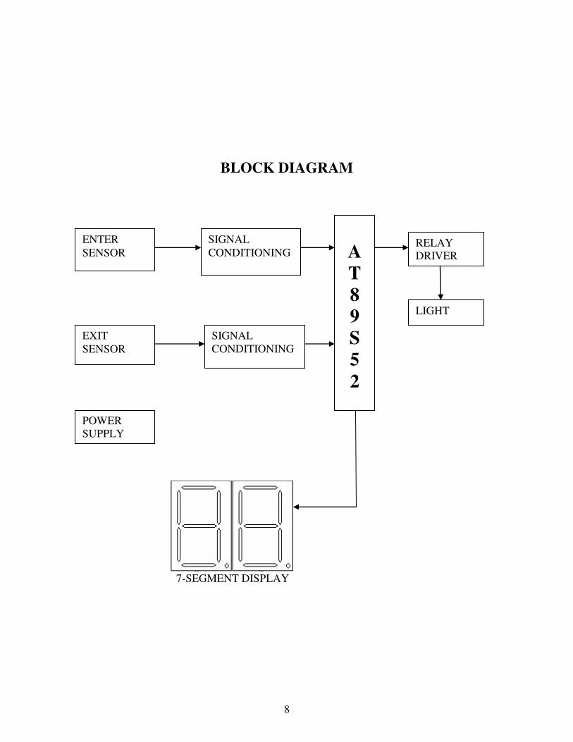
BLOCK DIAGRAM
7-SEGMENT DISPLAY
ENTER
SENSOR
SIGNAL
CONDITIONING
EXIT
SENSOR
SIGNAL
CONDITIONING
A
T
8
9
S
5
2
RELAY
DRIVER
LIGHT
POWER
SUPPLY
9
BLOCK DIAGRAM DESCRIPTION
The basic block diagram of the bidirectional visitor counter with automatic light
controller is shown in the above figure. Mainly this block diagram consists of the
following essential blocks.
1. Power Supply
2. Entry and Exit sensor circuit
3. AT89S52 micro-controller
4. Relay driver circuit
1. Power Supply:-
Here we used +12V and +5V dc power supply. The main function of this block
is to provide the required amount of voltage to essential circuits. +12V is given to
relay driver. To get the +5V dc power supply we have used here IC 7805, which
provides the +5V dc regulated power supply.
2. Enter and Exit Circuits:-
This is one of the main part of our project. The main intention of this block is to
sense the person. For sensing the person we are using a TSOP 1738 sensor. By
using this sensor and its related circuit diagram we can count the number of
persons.

10
3. 89S52 Microcontroller:-
It is a low-power, high performance CMOS 8-bit microcontroller with 8KB of
Flash Programmable and Erasable Read Only Memory (PEROM). The device is
manufactured using Atmel’s high-density nonvolatile memory technology and is
compatible with the MCS-51TM
instruction set and pin out. The on-chip Flash
allows the program memory to be reprogrammed in-system or by a conventional
nonvolatile memory programmer. By combining a versatile 8-bit CPU with Flash
on a monolithic chip, the Atmel AT89S52 is a powerful Microcontroller, which
provides a highly flexible and cost effective solution for many embedded control
applications.
4. Relay Driver Circuit:-
This block has the potential to drive the various controlled devices. In this block
mainly we are using the transistor and the relays. One relay driver circuit we are
using to control the light. Output signal from AT89S52 is given to the base of the
transistor, which energizes the particular relay, because of this, appropriate device
is selected and which performs its allotted function.
11
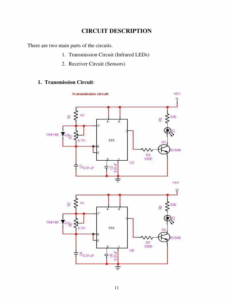
CIRCUIT DESCRIPTION
There are two main parts of the circuits.
1. Transmission Circuit (Infrared LEDs)
2. Receiver Circuit (Sensors)
1. Transmission Circuit:

12
This circuit diagram shows how a 555 timer IC, configured to function as a basic
astable multivibrator. The astable multivibrator generates a square wave, the period
of which is determined by the circuit external to IC 555. The astable multivibrator
does not require any external trigger to change the state of the output. Hence the
name free running oscillator. The time during which the output is either high or
low is determined by the two resistors and a capacitor which are externally
connected to the 555 timer.
IR Transmission circuit is used to generate the modulated 36 kHz IR signal.
The IC555 in the transmitter side is to generate 36 kHz square wave. Adjust the
preset in the transmitter to get a 38 kHz signal at the o/p. Then you point it over the
sensor and its o/p will go low when it senses the IR signal of 38 kHz.
13
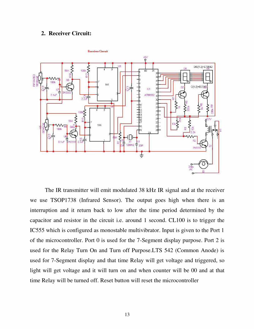
2. Receiver Circuit:
The IR transmitter will emit modulated 38 kHz IR signal and at the receiver
we use TSOP1738 (Infrared Sensor). The output goes high when there is an
interruption and it return back to low after the time period determined by the
capacitor and resistor in the circuit i.e. around 1 second. CL100 is to trigger the
IC555 which is configured as monostable multivibrator. Input is given to the Port 1
of the microcontroller. Port 0 is used for the 7-Segment display purpose. Port 2 is
used for the Relay Turn On and Turn off Purpose.LTS 542 (Common Anode) is
used for 7-Segment display and that time Relay will get voltage and triggered, so
light will get voltage and it will turn on and when counter will be 00 and at that
time Relay will be turned off. Reset button will reset the microcontroller
14
LIST OF COMPONENTS
Microcontroller – AT89S52
IC – 7805
Sensor – TSOP 1738 (Infrared Sensor)
Transformer – 12-0-12, 500 mA
Preset – 4.7K
Disc capacitor – 104,33pF
Reset button switch
Rectifier diode – IN4148
Transistor – BC 547, 2N2222
7-Segment Display
15
DESCRIPTION OF THE COMPONENTS USED
1. Microcontroller AT89S52
The AT89S52 is a low-power, high-performance CMOS 8-bit
microcontroller with 8K bytes of in-system programmable Flash memory. The
device is manufactured using Atmel’s high-density nonvolatile memory
technology and is compatible with the Industry-standard 80C51 instruction set and
pin out. The on-chip Flash allows the program memory to be reprogrammed in-
system or by a conventional nonvolatile memory pro-grammar. By combining a
versatile 8-bit CPU with in-system programmable Flash on a monolithic chip, the
Atmel AT89S52 is a powerful microcontroller which provides a highly-flexible
and cost-effective solution to many embedded control applications.
The AT89S52 provides the following standard features: 8K bytes of Flash,
256 bytes of RAM, 32 I/O lines, Watchdog timer, two data pointers, three 16-bit
timer/counters, a six-vector two-level interrupt architecture, a full duplex serial
port, on-chip oscillator, and clock circuitry. In addition, the AT89S52 is designed
with static logic for operation down to zero frequency and supports two software
selectable power saving modes. The Idle Mode stops the CPU while allowing the
RAM, timer/counters, serial port, and interrupt system to continue functioning. The
Power-down mode saves the RAM contents but freezes the oscillator, disabling all
other chip functions until the next interrupt or hardware reset.

16
FEATURES:
8 KB Reprogrammable flash.
32 Programmable I/O lines.
16 bit Timer/Counter—3.
8 Interrupt sources.
Power range: 4V – 5.5V
Endurance : 1000 Writes / Erase cycles
Fully static operation: 0 Hz to 33 MHz
Three level program memory lock
Power off flag
Full duplex UART serial channel
Low power idle and power down modes
Interrupt recovery from power down modes
256 KB internal RAM
Dual data pointer
17
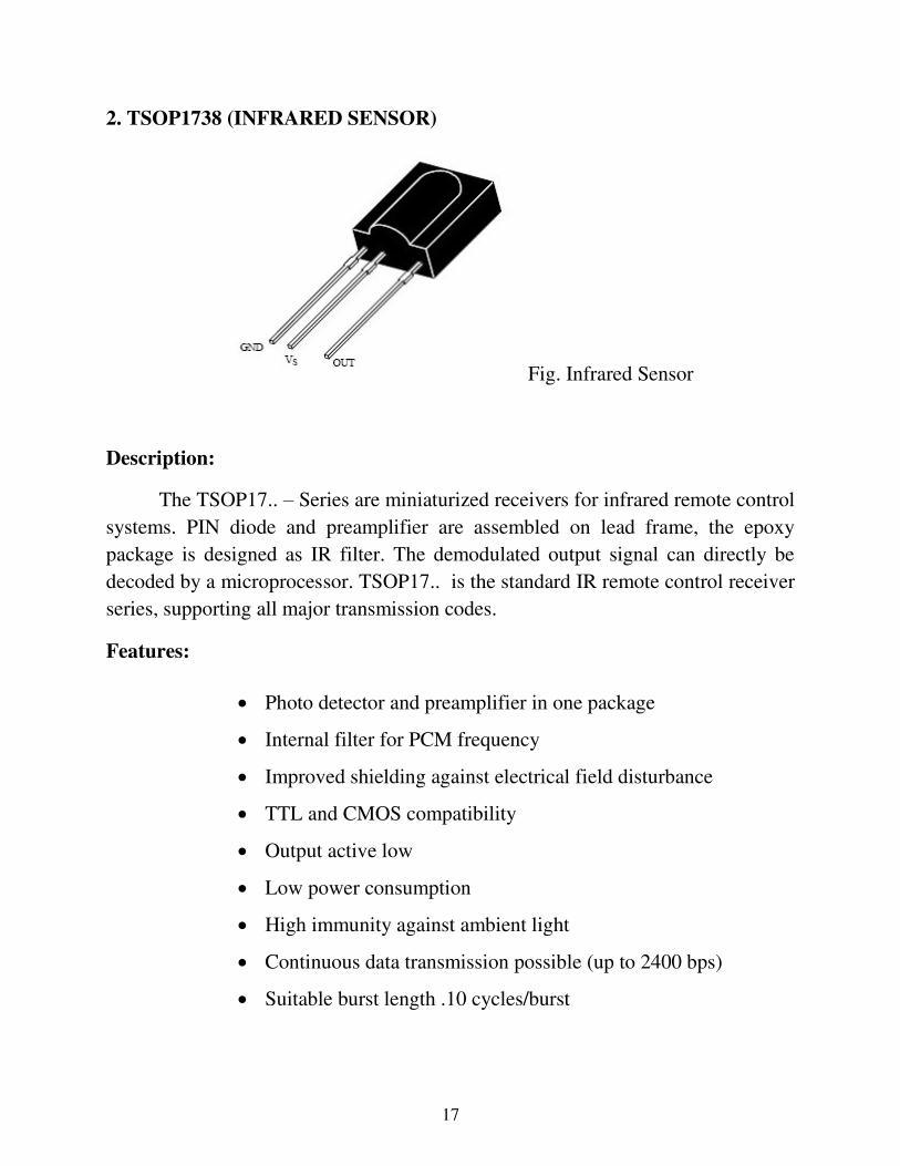
2. TSOP1738 (INFRARED SENSOR)
Fig. Infrared Sensor
Description:
The TSOP17.. – Series are miniaturized receivers for infrared remote control
systems. PIN diode and preamplifier are assembled on lead frame, the epoxy
package is designed as IR filter. The demodulated output signal can directly be
decoded by a microprocessor. TSOP17.. is the standard IR remote control receiver
series, supporting all major transmission codes.
Features:
Photo detector and preamplifier in one package
Internal filter for PCM frequency
Improved shielding against electrical field disturbance
TTL and CMOS compatibility
Output active low
Low power consumption
High immunity against ambient light
Continuous data transmission possible (up to 2400 bps)
Suitable burst length .10 cycles/burst
18
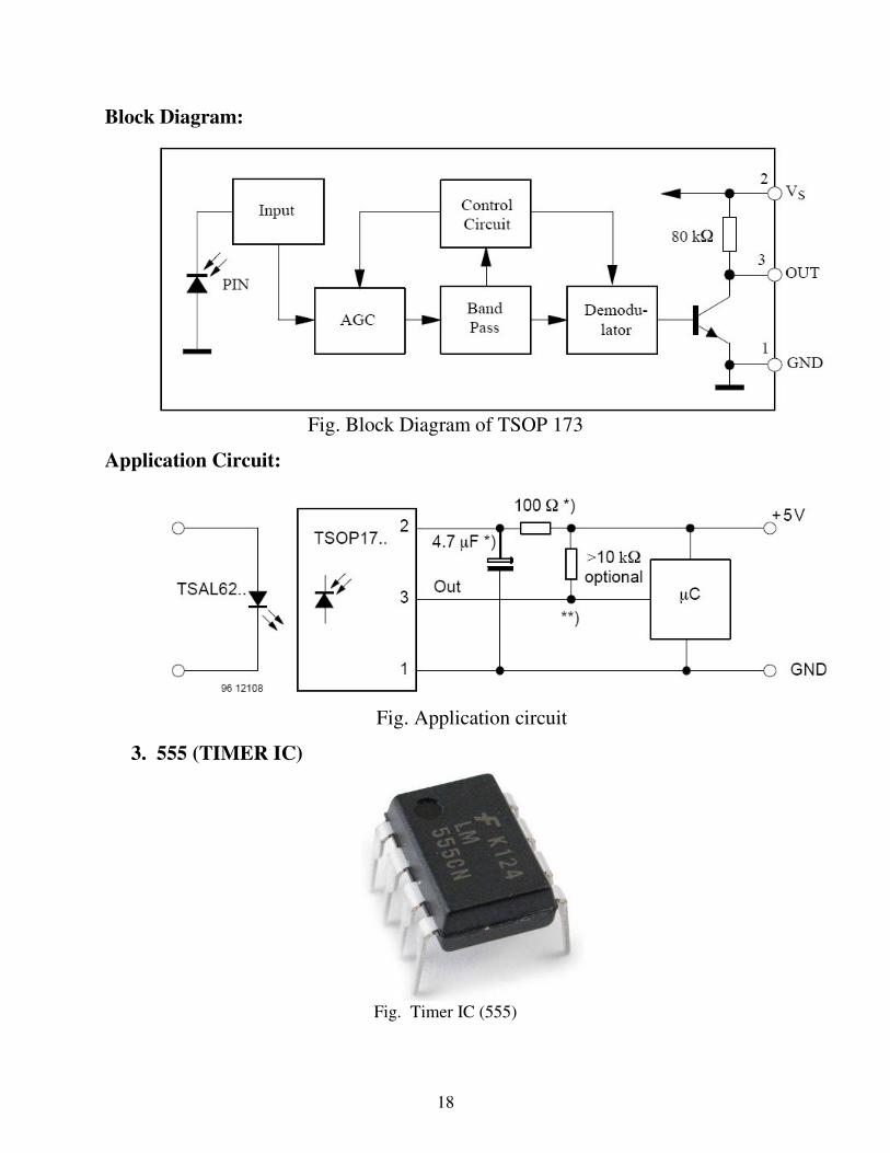
Block Diagram:
Fig. Block Diagram of TSOP 173
Application Circuit:
Fig. Application circuit
3. 555 (TIMER IC)
Fig. Timer IC (555)

19
Description:
The LM555 is a highly stable device for generating accurate time delays
or oscillation. Additional terminals are provided for triggering or resetting if
desired. In the time delay mode of operation, the time is precisely controlled by
one external resistor and capacitor. For astable operation as an oscillator, the free
running frequency and duty cycle are accurately controlled with two external
resistors and one capacitor. The circuit may be triggered and reset on falling
waveforms, and the output circuit can source or sink up to 200mA or drive TTL
circuits.
Features:
Direct replacement for SE555/NE555
Timing from microseconds through hours
Operates in both astable and monostable modes
Adjustable duty cycle
Output can source or sink 200 mA
Output and supply TTL compatible
Temperature stability better than 0.005% per °C
Normally on and normally off output
Available in 8-pin MSOP package
Applications:
Precision timing
Pulse generation
Sequential timing
20
Time delay generation
Pulse width modulation
Pulse position modulation
Linear ramp generator
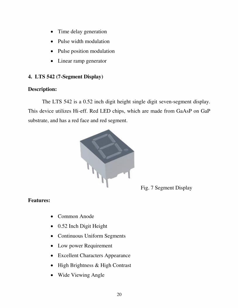
4. LTS 542 (7-Segment Display)
Description:
The LTS 542 is a 0.52 inch digit height single digit seven-segment display.
This device utilizes Hi-eff. Red LED chips, which are made from GaAsP on GaP
substrate, and has a red face and red segment.
Fig. 7 Segment Display
Features:
Common Anode
0.52 Inch Digit Height
Continuous Uniform Segments
Low power Requirement
Excellent Characters Appearance
High Brightness & High Contrast
Wide Viewing Angle
21
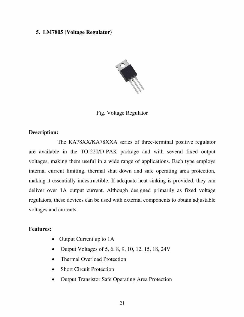
5. LM7805 (Voltage Regulator)
Fig. Voltage Regulator
Description:
The KA78XX/KA78XXA series of three-terminal positive regulator
are available in the TO-220/D-PAK package and with several fixed output
voltages, making them useful in a wide range of applications. Each type employs
internal current limiting, thermal shut down and safe operating area protection,
making it essentially indestructible. If adequate heat sinking is provided, they can
deliver over 1A output current. Although designed primarily as fixed voltage
regulators, these devices can be used with external components to obtain adjustable
voltages and currents.
Features:
Output Current up to 1A
Output Voltages of 5, 6, 8, 9, 10, 12, 15, 18, 24V
Thermal Overload Protection
Short Circuit Protection
Output Transistor Safe Operating Area Protection
22
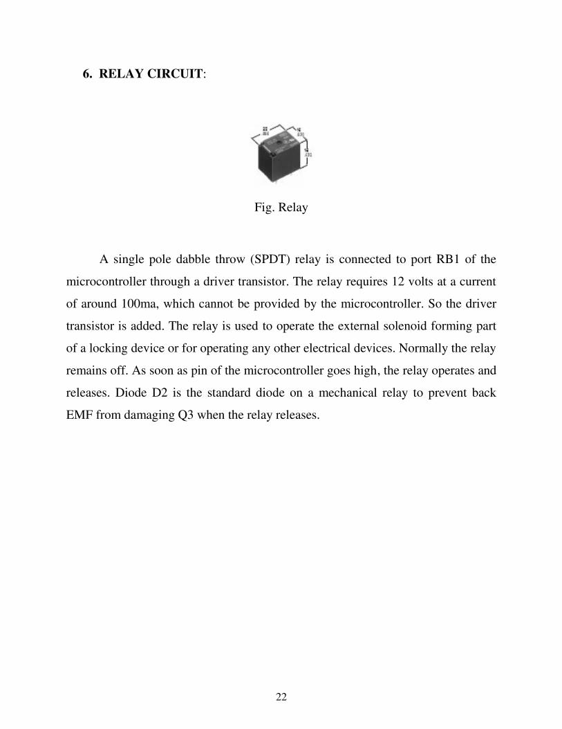
6. RELAY CIRCUIT:
Fig. Relay
A single pole dabble throw (SPDT) relay is connected to port RB1 of the
microcontroller through a driver transistor. The relay requires 12 volts at a current
of around 100ma, which cannot be provided by the microcontroller. So the driver
transistor is added. The relay is used to operate the external solenoid forming part
of a locking device or for operating any other electrical devices. Normally the relay
remains off. As soon as pin of the microcontroller goes high, the relay operates and
releases. Diode D2 is the standard diode on a mechanical relay to prevent back
EMF from damaging Q3 when the relay releases.
23
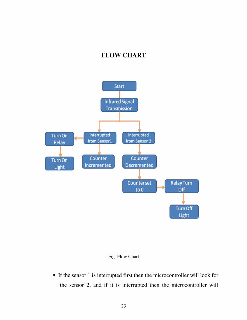
FLOW CHART
Fig. Flow Chart
If the sensor 1 is interrupted first then the microcontroller will look for
the sensor 2, and if it is interrupted then the microcontroller will

24
increment the count and switch on the relay, if it is first time
interrupted.
If the sensor 2 is interrupted first then the microcontroller will look for
the sensor 1, and if it is interrupted then the microcontroller will
decrement the count.
When the last person leaves the room then counter goes to 0 and that
time the relay will turn off, and light will be turned off.
PROGRAM
// Program to make a bidirectional visitor counter using IR sensor
#include <reg51.h>
#define msec 1
unsigned int num=0;
sbit dig_ctrl_4=P2^6; //declare the control pins of seven segments
sbit dig_ctrl_3=P2^5;
sbit dig_ctrl_2=P2^6;
sbit dig_ctrl_1=P2^5;
sbit relay1 = P2^0;
sbit pin = P3^7;
unsigned char
digi_val[11]={0xFE,0x18,0x6D,0x3d,0x1B,0X37,0x77,0x1C,0xfF,0x3F};
unsigned int dig_1,dig_2,dig_3,dig_4,test=0;
unsigned char dig_disp=0;
sbit up=P1^0; //up pin to make counter count up
sbit down=P1^1; //down pin to make counter count down
void delay(int x)
{
char y = 200;
pin = !pin;
while((x--))
{
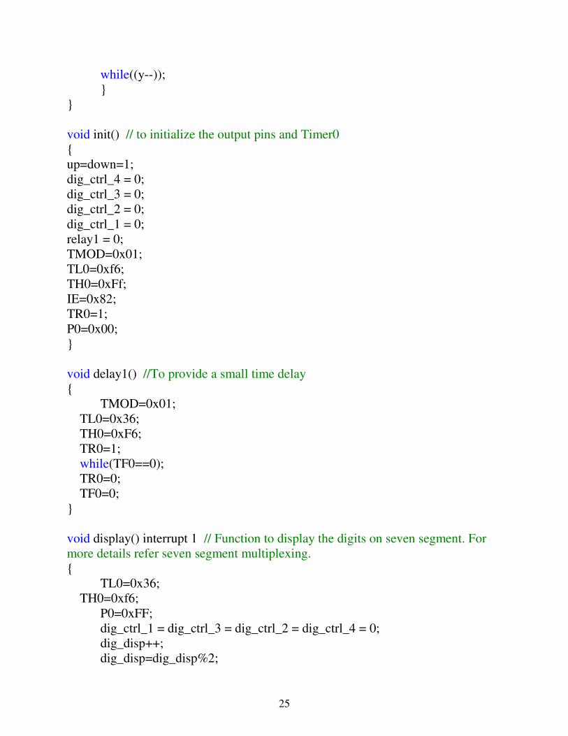
25
while((y--));
}
}
void init() // to initialize the output pins and Timer0
{
up=down=1;
dig_ctrl_4 = 0;
dig_ctrl_3 = 0;
dig_ctrl_2 = 0;
dig_ctrl_1 = 0;
relay1 = 0;
TMOD=0x01;
TL0=0xf6;
TH0=0xFf;
IE=0x82;
TR0=1;
P0=0x00;
}
void delay1() //To provide a small time delay
{
TMOD=0x01;
TL0=0x36;
TH0=0xF6;
TR0=1;
while(TF0==0);
TR0=0;
TF0=0;
}
void display() interrupt 1 // Function to display the digits on seven segment. For
more details refer seven segment multiplexing.
{
TL0=0x36;
TH0=0xf6;
P0=0xFF;
dig_ctrl_1 = dig_ctrl_3 = dig_ctrl_2 = dig_ctrl_4 = 0;
dig_disp++;
dig_disp=dig_disp%2;
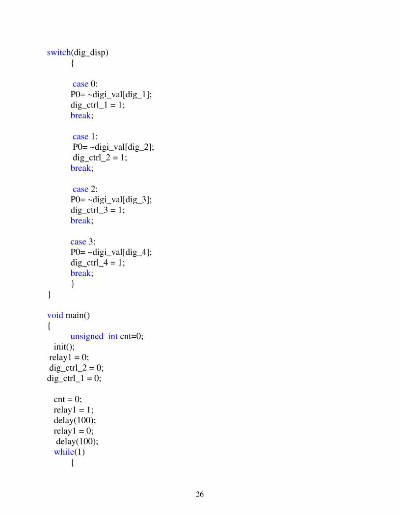
26
switch(dig_disp)
{
case 0:
P0= ~digi_val[dig_1];
dig_ctrl_1 = 1;
break;
case 1:
P0= ~digi_val[dig_2];
dig_ctrl_2 = 1;
break;
case 2:
P0= ~digi_val[dig_3];
dig_ctrl_3 = 1;
break;
case 3:
P0= ~digi_val[dig_4];
dig_ctrl_4 = 1;
break;
}
}
void main()
{
unsigned int cnt=0;
init();
relay1 = 0;
dig_ctrl_2 = 0;
dig_ctrl_1 = 0;
cnt = 0;
relay1 = 1;
delay(100);
relay1 = 0;
delay(100);
while(1)
{
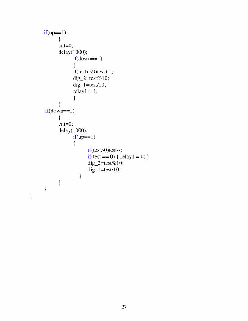
27
if(up==1)
{
cnt=0;
delay(1000);
if(down==1)
{
if(test<99)test++;
dig_2=test%10;
dig_1=test/10;
relay1 = 1;
}
}
if(down==1)
{
cnt=0;
delay(1000);
if(up==1)
{
if(test>0)test--;
if(test == 0) { relay1 = 0; }
dig_2=test%10;
dig_1=test/10;
}
}
}
}

28
PCB FABRICATION
Printed Circuit Board (PCB) is piece of art. The performance of an electronic
circuit depends on the layout and the design of PCB. A PCB mechanically supports
and connects components by conductive pathways, etched from copper sheets
laminated on to insulated substrate. PCB ape used to rotate electrical currents and
signals through copper tracts which are firmly bonded to an insulating base.
PCB Fabrication involves the following steps:
1. Drawing the layout of the PCB in the paper. The track layout of the
Electronic circuit should be made in such manner that the paths are in easy
routes. It is then transferred to a Mylar sheet. The sheet is then touched with
black ink.
2. The solder side of the Mylar sheet is placed on the shiny side of the five-
Star sheet and is placed in a frame. Then it is exposed to sunlight with Mylar
sheet facing the sunlight.
3. The exposed five- star sheet is put in Hydrogen Peroxide solution. Then it is
put in hot water and shook till unexposed region becomes transparent.
4. This is put in cold water and then the rough side is stuck on to the silk
screen. This is then pressed and dried well.
5. The plastic sheet of the five-star sheet is removed leaving the pattern on the
screen.
6. A copper clad sheet is cut to the size and cleaned. This is placed under
screen.
7. As it resistant ink if spread on the screen so that a pattern of tracks and a pad
is obtained on a copper clad sheet. It is then dried.
8. The dried sheet is then etched using Ferric chloride solution (32Baume) till
all the unwanted Copper is etched away. Swish the board to keep each fluid
moving. Lift up the PCB and check whether all the unwanted Copper is
removed. Etching is done by immersing the marked copper clad in Ferric
Chloride solution after that the etched sheet is dried.
9. The unwanted resist ink is removed using Sodium Hydroxide solution Holes
are them dried.

29
PCB PARAMETERS
Copper thickness - 72mil (1mm=39.37 mils)
Track width - 60mil
Clearance - 60mil
Pad width - 86mil
Pad height - 86mil
Pad shape - Oval
Pad hole size - 25mil
On board - Through
Hole size - 0.9mm (36mil)
Base - Paper phenolic, Hylam
PCB Quality - FRC4
SOLDERING
Soldering is the process of joining metals by using lower melting point to
weld or alloy with joining surface.
SOLDER
Solder is the joining material that melts below 427 degree connections
between components. The popularly used solders are alloys of tin (Sn) and lead
(Pb) that melts below the melting point of tin.
Types:
1. Rosin core: - 60/40 Sn/Pb solders are the most common types used for
electronics assembly. These solders are available in various diameters and
are most appropriate for small electronics work (0.02’’-0.05‖ dia is recommended)
30
2. Lead free: - lead free solders are used as more environmental-friendly
substitutes for leaded solder, but they are typically not as easy to use mainly
because of their higher melting point and poorer wetting properties.
3. Silver: - Silver solders are typically used for low resistance connections but
they have a higher melting point and are expensive than Sn/ Pb solders.
4. Acid –core: - Acid-core solders should not be used for electronics. They are
intended for plumbing or non-electronics assembly work. The acid-core flux
will cause corrosion of circuitry and can damage components.
5. Other special solders :-
Various melting point eutectics: These special solders are
typically used for non-electronic assembly of difficult to
construct mechanical items that must be assembled in a particular
sequence.
Paste solders: These solders are used in the field application or in
specialized manufacturing application.
FLUX
In order to make the surface accept the solder readily, the components
terminals should be free oxides and other obstructing films. The lead should be
cleaned chemically or by abrasion using blades or knives.
Small amount of lead coating can be done on the portion of the leads using
soldering iron. This process is called thinning. Zinc chloride or ammonium
chloride separately or in combination is mostly used as fluxes. These are available
in petroleum jelly as paste flux.
31
Flux medium used to remove the degree of wetting. The desirable properties of
flux are:-
It should provide a liquid cover over the materials and exclude air
gap up to the soldering temperature.
It should dissolve any Oxide on the metal surface.
It should be easily replaced from the metal by the molten soldering
operation
Residue should be removable after completing soldering operation.
The most common flux used in hand soldering of electronic components is
rosin, a combination of mild organic acids extracted from pine tree.
SOLDERING IRON
It is a tool used to melt the solder and apply it at the joints in the circuit. It
operates in 230V supply. The iron at the tip gets heated while few minutes. The
50W and 25W soldering irons are commonly used for soldering of electronics
circuit.
SOLDERING STEPS
1. Make the layout of the component in the circuit. Plug in the chord of the
soldering iron the mains to get heated.
2. Straighten and clean the component leads using a blade or a knife.
3. Mount the components on the PCB by bending the leads of the
components. Use nose pliers.
4. Apply flux on the joints and solder the joints. Soldering must be in
minimum time to avoid dry soldering and heating up of the components.
5. Wash the residue using water and brush.
6. Solder joins should be inspected when completed to determine if they
have been properly made.
32
CHARACTERISTICS OF A GOOD SOLDER JOINTS:
A. Shiny surface.
B. Good, smooth fillet.
CHARACTERISTICS OF A POOR SOLDER JOINTS:
1. Dull or crystallized surface: This is an indicator of a cold solder joint.
Cold solder joint result from moving the component after soldering has
been removed, but before the solder has hardened. Cold solder joints may
work at first, but will eventually fail.
2. Air pocket: Air pocket (voids) result from incomplete wetting of surface,
allowing air to be in contact with the connecting metals. This will cause
oxidation of the joints and eventual failure. Blow holes can occur due to
vaporization of the moisture on the surface of the board and existing
through the molten solder. Boards should be clean and dry. Prior to
soldering. Ethanol (100%) can be used as a moisture chaser if boards are
wet prior to soldering.
3. Dimples: Dimples in the surface do not always indicate a serious
problem, but they should be avoided since they are precursors to voids.
4. Floaters: Black spots ―floating‖ in the soldering fillet should be avoided
because they indicate contamination and a potential for failure as in the
case of voids. These black spots usually result from overheated (burnt)
Rosin or other contaminants such as burnt wire insulation. Maintaining a
clean tip will help to avoid these problems.
5. Balls: A solder balls, instead of a fillet can occur if the trace was heated
but the leads was not (vice versa). This prevents proper wetting of both
surfaces and result in solder being attached to only one surface
(component or trace)
6. Excess solder: Excess solder usage can cover up other potential problems
and should be avoided. It can lead to solder bridges. In addition, spherical
solder joints can result from the application of too much solder.
33
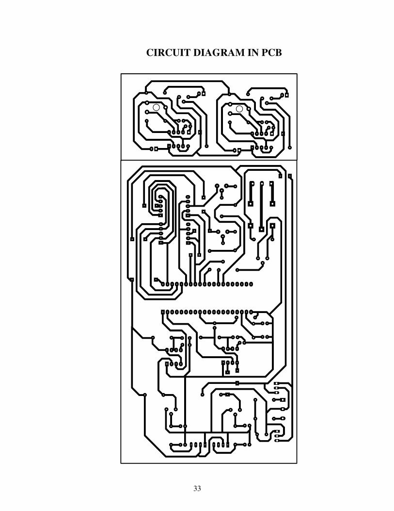
CIRCUIT DIAGRAM IN PCB