andescore ax45mp-1c processor reference manual
TRANSCRIPT
Document Number UM248-12Date Issued 2022-03-25
Copyright © 2022 Andes Technology Corporation.All rights reserved.
AndesCoreAX45MP-1C Processor
Reference Manual
AndesCore AX45MP-1C Processor Reference Manual
Copyright Notice
Copyright © 2022 Andes Technology Corporation. All rights reserved.
AndesCore™, AndeSight™, AndeShape™, AndESLive™, AndeSoft™, AndeStar™, Andes Custom Ex-tension™, CoDense™, StackSafe™, QuickNap™, AndesClarity™, AndeSim™, AndeSysC™, Andes-Embedded and Driving Innovations are trademarks owned by Andes Technology Corporation. Allother trademarks used herein are the property of their respective owners.
The product described herein is subject to continuous development and improvement. Thus, allinformation herein is provided by Andes in good faith but without warranties. This document isintended only to assist the reader in the use of the product. Andes Technology Corporation shallnot be liable for any loss or damage arising from the use of any information in this document, orany incorrect use of the product.
Contact Information
Should you have any problems with the information contained herein, you may contact AndesTechnology Corporation through at [email protected]
Please include the following information in your inquiries:
• the document title
• the document number
• the page number(s) to which your comments apply
• a concise explanation of the problem.
General suggestions for improvements are welcome.
The information contained herein is the exclusive property of Andes Technology Co. and shall not be distributed,reproduced, or disclosed in whole or in part without prior written permission of Andes Technology Corporation.AndesCore_AX45MP-1C_UM248_V1.2
Page ii
AndesCore AX45MP-1C Processor Reference Manual
Revision History
Rev. Rev. Date Revised Content
1.2 2022-03-25 Third Release for CPU Revision 5.0.0.• Revise disclaimers on Copyright Notice page
1.1 2022-03-01 Second Release for CPU Revision 5.0.0.• Revise wording of nceplmt100 and ncepldm200 in section 19.2.1 and
20.3.12 respectively *
1.0 2021-12-17 First Release for CPU Revision 5.0.0.
The information contained herein is the exclusive property of Andes Technology Co. and shall not be distributed,reproduced, or disclosed in whole or in part without prior written permission of Andes Technology Corporation.AndesCore_AX45MP-1C_UM248_V1.2
Page iii
AndesCore AX45MP-1C Processor Reference Manual
Contents
Revision History iii
List of Figures xiv
List of Tables xv
1 Overview 11.1 AX45MP-1C Processor Features . . . . . . . . . . . . . . . . . . . . . . . . . . . . . . . 11.2 Block Diagram . . . . . . . . . . . . . . . . . . . . . . . . . . . . . . . . . . . . . . . . 41.3 Major Components . . . . . . . . . . . . . . . . . . . . . . . . . . . . . . . . . . . . . 41.4 Pipeline Stages and Activities . . . . . . . . . . . . . . . . . . . . . . . . . . . . . . . . 5
2 Instruction Set Overview 72.1 Introduction . . . . . . . . . . . . . . . . . . . . . . . . . . . . . . . . . . . . . . . . . 72.2 Integer Registers . . . . . . . . . . . . . . . . . . . . . . . . . . . . . . . . . . . . . . . 72.3 Atomic Instructions . . . . . . . . . . . . . . . . . . . . . . . . . . . . . . . . . . . . . 8
2.3.1 Load-Reserved/Store-Conditional Instruction . . . . . . . . . . . . . . . . . . 82.3.2 Atomic Memory Operation Instruction . . . . . . . . . . . . . . . . . . . . . . 8
2.4 Misaligned Memory Access . . . . . . . . . . . . . . . . . . . . . . . . . . . . . . . . . 82.4.1 Exceptions . . . . . . . . . . . . . . . . . . . . . . . . . . . . . . . . . . . . . 9
2.5 Floating-Point ISA Extension . . . . . . . . . . . . . . . . . . . . . . . . . . . . . . . . 92.5.1 Support for Half-Precision and BFLOAT16 Formats . . . . . . . . . . . . . . . 9
2.6 DSP ISA Extension . . . . . . . . . . . . . . . . . . . . . . . . . . . . . . . . . . . . . . 10
3 Branch Prediction Unit 11
4 Memory Management Unit 124.1 Introduction . . . . . . . . . . . . . . . . . . . . . . . . . . . . . . . . . . . . . . . . . 124.2 Address Translation . . . . . . . . . . . . . . . . . . . . . . . . . . . . . . . . . . . . . 124.3 Translation Lookaside Buffer . . . . . . . . . . . . . . . . . . . . . . . . . . . . . . . . 14
4.3.1 Instruction uTLB (iTLB) . . . . . . . . . . . . . . . . . . . . . . . . . . . . . . 144.3.2 Data uTLB (dTLB) . . . . . . . . . . . . . . . . . . . . . . . . . . . . . . . . . 144.3.3 Shared TLB (STLB) . . . . . . . . . . . . . . . . . . . . . . . . . . . . . . . . 144.3.4 Replacement Policy . . . . . . . . . . . . . . . . . . . . . . . . . . . . . . . . 14
4.4 Page Table Walker (PTW) . . . . . . . . . . . . . . . . . . . . . . . . . . . . . . . . . . 144.4.1 Introduction . . . . . . . . . . . . . . . . . . . . . . . . . . . . . . . . . . . . 144.4.2 Page Table Address Formation . . . . . . . . . . . . . . . . . . . . . . . . . . . 15
4.5 Attributes for Address Spaces . . . . . . . . . . . . . . . . . . . . . . . . . . . . . . . . 15
The information contained herein is the exclusive property of Andes Technology Co. and shall not be distributed,reproduced, or disclosed in whole or in part without prior written permission of Andes Technology Corporation.AndesCore_AX45MP-1C_UM248_V1.2
Page iv
AndesCore AX45MP-1C Processor Reference Manual
4.5.1 Attributes for Virtual Memory Pages . . . . . . . . . . . . . . . . . . . . . . . 15
5 Local Memory 175.1 Introduction . . . . . . . . . . . . . . . . . . . . . . . . . . . . . . . . . . . . . . . . . 175.2 Local Memory Spaces . . . . . . . . . . . . . . . . . . . . . . . . . . . . . . . . . . . . 175.3 Local Memory Address Range . . . . . . . . . . . . . . . . . . . . . . . . . . . . . . . 185.4 Local Memory Usage Constraints . . . . . . . . . . . . . . . . . . . . . . . . . . . . . . 19
6 Local Memory Slave Port 206.1 Introduction . . . . . . . . . . . . . . . . . . . . . . . . . . . . . . . . . . . . . . . . . 206.2 Support for Soft Error Protection . . . . . . . . . . . . . . . . . . . . . . . . . . . . . . 20
7 Level-1 Caches 217.1 Introduction . . . . . . . . . . . . . . . . . . . . . . . . . . . . . . . . . . . . . . . . . 217.2 Cache Replacement Policy . . . . . . . . . . . . . . . . . . . . . . . . . . . . . . . . . . 227.3 I-Cache . . . . . . . . . . . . . . . . . . . . . . . . . . . . . . . . . . . . . . . . . . . . 22
7.3.1 I-Cache Fill Operation . . . . . . . . . . . . . . . . . . . . . . . . . . . . . . . 227.3.2 I-Cache Prefetch . . . . . . . . . . . . . . . . . . . . . . . . . . . . . . . . . . 237.3.3 I-Cache TAG SRAM Fields . . . . . . . . . . . . . . . . . . . . . . . . . . . . . 23
7.4 D-Cache . . . . . . . . . . . . . . . . . . . . . . . . . . . . . . . . . . . . . . . . . . . 247.4.1 Cache Access Latency . . . . . . . . . . . . . . . . . . . . . . . . . . . . . . . 247.4.2 D-Cache Fill Operations . . . . . . . . . . . . . . . . . . . . . . . . . . . . . . 247.4.3 D-Cache Eviction Operations . . . . . . . . . . . . . . . . . . . . . . . . . . . 257.4.4 D-Cache Write Buffers . . . . . . . . . . . . . . . . . . . . . . . . . . . . . . . 257.4.5 D-Cache TAG SRAM Fields . . . . . . . . . . . . . . . . . . . . . . . . . . . . 26
7.5 FENCE/FENCE.I Operations . . . . . . . . . . . . . . . . . . . . . . . . . . . . . . . . 277.6 CCTL Operations . . . . . . . . . . . . . . . . . . . . . . . . . . . . . . . . . . . . . . . 27
7.6.1 Invalidating Cache Blocks (L1D_VA_INVAL, L1I_VA_INVAL, L1D_IX_INVAL,L1I_IX_INVAL) . . . . . . . . . . . . . . . . . . . . . . . . . . . . . . . . . . . 28
7.6.2 Writing Back Cache Blocks (L1D_VA_WB, L1D_IX_WB, L1D_WB_ALL) . . . . 287.6.3 Writing Back & Invalidating Cache Blocks (L1D_VA_WBINVAL, L1D_IX_WBIN-
VAL, L1D_WBINVAL_ALL) . . . . . . . . . . . . . . . . . . . . . . . . . . . . . 297.6.4 Filling and Locking Cache Blocks (L1D_VA_LOCK, L1I_VA_LOCK) . . . . . . . 297.6.5 Unlocking Cache Blocks (L1D_VA_UNLOCK, L1I_VA_UNLOCK) . . . . . . . . 297.6.6 Reading Tag Data from Caches (L1D_IX_RTAG, L1I_IX_RTAG) . . . . . . . . . 297.6.7 Reading Data from D-Cache (L1D_IX_RDATA) . . . . . . . . . . . . . . . . . . 307.6.8 Reading Data from I-Caches (L1I_IX_RDATA) . . . . . . . . . . . . . . . . . . 307.6.9 Writing Tag Data to Caches (L1D_IX_WTAG, L1I_IX_WTAG) . . . . . . . . . . 307.6.10 Writing Data to D-Cache (L1D_IX_WDATA) . . . . . . . . . . . . . . . . . . . 307.6.11 Writing Data to I-Caches (L1I_IX_WDATA) . . . . . . . . . . . . . . . . . . . . 31
The information contained herein is the exclusive property of Andes Technology Co. and shall not be distributed,reproduced, or disclosed in whole or in part without prior written permission of Andes Technology Corporation.AndesCore_AX45MP-1C_UM248_V1.2
Page v
AndesCore AX45MP-1C Processor Reference Manual
7.6.12 Invalidating All Cache Blocks (L1D_INVAL_ALL) . . . . . . . . . . . . . . . . 317.6.13 Writing Back All Cache Blocks (L1D_WB_ALL) . . . . . . . . . . . . . . . . . 317.6.14 Writing Back & Invalidating All Cache Blocks (L1D_WBINVAL_ALL) . . . . . . 31
7.7 Supervisor/User CCTL Operations . . . . . . . . . . . . . . . . . . . . . . . . . . . . . 31
8 Level-2 Cache 338.1 Introduction . . . . . . . . . . . . . . . . . . . . . . . . . . . . . . . . . . . . . . . . . 33
8.1.1 Multi-Cycle RAM Support . . . . . . . . . . . . . . . . . . . . . . . . . . . . . 338.1.2 L2-Cache Prefetch . . . . . . . . . . . . . . . . . . . . . . . . . . . . . . . . . 348.1.3 Asynchronous Error . . . . . . . . . . . . . . . . . . . . . . . . . . . . . . . . 348.1.4 Cache Control Operation . . . . . . . . . . . . . . . . . . . . . . . . . . . . . 34
8.2 L2-Cache Organization . . . . . . . . . . . . . . . . . . . . . . . . . . . . . . . . . . . 358.2.1 Two Bank L2-Cache Structure . . . . . . . . . . . . . . . . . . . . . . . . . . . 35
8.3 L2C Programming Guide . . . . . . . . . . . . . . . . . . . . . . . . . . . . . . . . . . 358.4 L2-Cache Controller Registers . . . . . . . . . . . . . . . . . . . . . . . . . . . . . . . 36
8.4.1 Register Type . . . . . . . . . . . . . . . . . . . . . . . . . . . . . . . . . . . . 368.4.2 Summary of Registers . . . . . . . . . . . . . . . . . . . . . . . . . . . . . . . 368.4.3 Configuration Register . . . . . . . . . . . . . . . . . . . . . . . . . . . . . . . 388.4.4 Control Register . . . . . . . . . . . . . . . . . . . . . . . . . . . . . . . . . . 398.4.5 HPM Control Register 0 . . . . . . . . . . . . . . . . . . . . . . . . . . . . . . 428.4.6 HPM Control Register 1 . . . . . . . . . . . . . . . . . . . . . . . . . . . . . . 448.4.7 HPM Control Register 2 . . . . . . . . . . . . . . . . . . . . . . . . . . . . . . 458.4.8 HPM Control Register 3 . . . . . . . . . . . . . . . . . . . . . . . . . . . . . . 468.4.9 Asynchronous Error Register . . . . . . . . . . . . . . . . . . . . . . . . . . . 478.4.10 Error Register . . . . . . . . . . . . . . . . . . . . . . . . . . . . . . . . . . . . 488.4.11 CCTL Command Registers 0 – 3 . . . . . . . . . . . . . . . . . . . . . . . . . . 508.4.12 CCTL Access Line Registers 0 – 3 . . . . . . . . . . . . . . . . . . . . . . . . . 518.4.13 CCTL Status Register . . . . . . . . . . . . . . . . . . . . . . . . . . . . . . . . 538.4.14 CCTL TGT Data Registers 0 – 7 . . . . . . . . . . . . . . . . . . . . . . . . . . 548.4.15 CCTL TGT ECC Code Register . . . . . . . . . . . . . . . . . . . . . . . . . . . 568.4.16 HPM Counter Registers 0 – 31 . . . . . . . . . . . . . . . . . . . . . . . . . . 57
9 L1 Memory Error Protection 599.1 Parity/ECC Control Mode . . . . . . . . . . . . . . . . . . . . . . . . . . . . . . . . . . 59
9.1.1 Disable Parity/ECC . . . . . . . . . . . . . . . . . . . . . . . . . . . . . . . . . 609.1.2 Generate Exceptions on Uncorrectable Parity/ECC Errors . . . . . . . . . . . . 609.1.3 Generate Exceptions on Parity/ECC Errors . . . . . . . . . . . . . . . . . . . . 61
9.2 Local Memory Protection . . . . . . . . . . . . . . . . . . . . . . . . . . . . . . . . . . 619.3 I-Cache Protection . . . . . . . . . . . . . . . . . . . . . . . . . . . . . . . . . . . . . . 619.4 D-Cache Protection . . . . . . . . . . . . . . . . . . . . . . . . . . . . . . . . . . . . . 62
The information contained herein is the exclusive property of Andes Technology Co. and shall not be distributed,reproduced, or disclosed in whole or in part without prior written permission of Andes Technology Corporation.AndesCore_AX45MP-1C_UM248_V1.2
Page vi
AndesCore AX45MP-1C Processor Reference Manual
9.5 Soft Error Injection . . . . . . . . . . . . . . . . . . . . . . . . . . . . . . . . . . . . . 629.5.1 ILM/DLM ECC Error Injection . . . . . . . . . . . . . . . . . . . . . . . . . . . 629.5.2 I-Cache Parity/ECC Error Injection . . . . . . . . . . . . . . . . . . . . . . . . 629.5.3 D-Cache ECC Error Injection . . . . . . . . . . . . . . . . . . . . . . . . . . . 63
10 Physical Memory Attributes 6410.1 Introduction . . . . . . . . . . . . . . . . . . . . . . . . . . . . . . . . . . . . . . . . . 6410.2 Static Physical Memory Attributes . . . . . . . . . . . . . . . . . . . . . . . . . . . . . 6410.3 Programmable Physical Memory Attributes . . . . . . . . . . . . . . . . . . . . . . . . 6410.4 Memory Access Ordering . . . . . . . . . . . . . . . . . . . . . . . . . . . . . . . . . . 6510.5 Non-Cacheable Memory and Device Accesses . . . . . . . . . . . . . . . . . . . . . . . 6510.6 Cacheable Memory Accesses to L1-Caches . . . . . . . . . . . . . . . . . . . . . . . . . 65
10.6.1 Write-Back . . . . . . . . . . . . . . . . . . . . . . . . . . . . . . . . . . . . . 6610.6.2 I-Cache Disabled Behaviors . . . . . . . . . . . . . . . . . . . . . . . . . . . . 6710.6.3 D-Cache Disabled Behaviors . . . . . . . . . . . . . . . . . . . . . . . . . . . . 6710.6.4 Debug Mode . . . . . . . . . . . . . . . . . . . . . . . . . . . . . . . . . . . . 67
10.7 Cacheable Memory Accesses to L2-Caches . . . . . . . . . . . . . . . . . . . . . . . . . 68
11 MemBoost 7011.1 Non-Blocking Memory Access . . . . . . . . . . . . . . . . . . . . . . . . . . . . . . . . 7011.2 D-Cache Write-Around Support . . . . . . . . . . . . . . . . . . . . . . . . . . . . . . . 7111.3 D-Cache Prefetch . . . . . . . . . . . . . . . . . . . . . . . . . . . . . . . . . . . . . . 72
12 Coherence Manager (CM) 74
13 Trap 7513.1 Introduction . . . . . . . . . . . . . . . . . . . . . . . . . . . . . . . . . . . . . . . . . 7513.2 Interrupt . . . . . . . . . . . . . . . . . . . . . . . . . . . . . . . . . . . . . . . . . . . 75
13.2.1 Additional Local Interrupts . . . . . . . . . . . . . . . . . . . . . . . . . . . . 7613.2.2 Interrupt Status and Masking . . . . . . . . . . . . . . . . . . . . . . . . . . . 76
13.3 Exception . . . . . . . . . . . . . . . . . . . . . . . . . . . . . . . . . . . . . . . . . . . 7613.4 Trap Handling . . . . . . . . . . . . . . . . . . . . . . . . . . . . . . . . . . . . . . . . 77
13.4.1 Entering the Trap Handler . . . . . . . . . . . . . . . . . . . . . . . . . . . . . 7713.4.2 Returning from the Trap Handler . . . . . . . . . . . . . . . . . . . . . . . . . 78
14 Reset and Non-Maskable Interrupts 7914.1 Reset . . . . . . . . . . . . . . . . . . . . . . . . . . . . . . . . . . . . . . . . . . . . . 7914.2 Non-Maskable Interrupts . . . . . . . . . . . . . . . . . . . . . . . . . . . . . . . . . . 79
15 Power Management 8015.1 Power Management Unit . . . . . . . . . . . . . . . . . . . . . . . . . . . . . . . . . . 80
The information contained herein is the exclusive property of Andes Technology Co. and shall not be distributed,reproduced, or disclosed in whole or in part without prior written permission of Andes Technology Corporation.AndesCore_AX45MP-1C_UM248_V1.2
Page vii
AndesCore AX45MP-1C Processor Reference Manual
15.2 Wait-For-Interrupt Mode . . . . . . . . . . . . . . . . . . . . . . . . . . . . . . . . . . 8015.3 Dynamic Frequency Scaling (DFS) . . . . . . . . . . . . . . . . . . . . . . . . . . . . . 8115.4 D-Cache Coherency . . . . . . . . . . . . . . . . . . . . . . . . . . . . . . . . . . . . . 81
15.4.1 Disable D-Cache Coherency . . . . . . . . . . . . . . . . . . . . . . . . . . . . 8115.4.2 Enable D-Cache Coherency . . . . . . . . . . . . . . . . . . . . . . . . . . . . 81
15.5 Disable All Clocks of a Core . . . . . . . . . . . . . . . . . . . . . . . . . . . . . . . . . 82
16 Control and Status Registers 8316.1 Introduction . . . . . . . . . . . . . . . . . . . . . . . . . . . . . . . . . . . . . . . . . 83
16.1.1 System Register Type . . . . . . . . . . . . . . . . . . . . . . . . . . . . . . . 8316.1.2 Reset Value . . . . . . . . . . . . . . . . . . . . . . . . . . . . . . . . . . . . . 8316.1.3 CSR Listing . . . . . . . . . . . . . . . . . . . . . . . . . . . . . . . . . . . . . 83
16.2 Machine Information Registers . . . . . . . . . . . . . . . . . . . . . . . . . . . . . . . 9116.2.1 Machine Vendor ID Register . . . . . . . . . . . . . . . . . . . . . . . . . . . . 9116.2.2 Machine Architecture ID Register . . . . . . . . . . . . . . . . . . . . . . . . . 9116.2.3 Machine Implementation ID Register . . . . . . . . . . . . . . . . . . . . . . . 9216.2.4 Hart ID Register . . . . . . . . . . . . . . . . . . . . . . . . . . . . . . . . . . 93
16.3 Machine Trap Related CSRs . . . . . . . . . . . . . . . . . . . . . . . . . . . . . . . . . 9316.3.1 Machine Status . . . . . . . . . . . . . . . . . . . . . . . . . . . . . . . . . . . 9316.3.2 Machine ISA Register . . . . . . . . . . . . . . . . . . . . . . . . . . . . . . . 9816.3.3 Machine Exception Delegation . . . . . . . . . . . . . . . . . . . . . . . . . . 9916.3.4 Machine Interrupt Delegation . . . . . . . . . . . . . . . . . . . . . . . . . . . 10216.3.5 Machine Interrupt Enable . . . . . . . . . . . . . . . . . . . . . . . . . . . . . 10416.3.6 Machine Trap Vector Base Address . . . . . . . . . . . . . . . . . . . . . . . . 10616.3.7 Machine Scratch Register . . . . . . . . . . . . . . . . . . . . . . . . . . . . . 10716.3.8 Machine Exception Program Counter . . . . . . . . . . . . . . . . . . . . . . . 10716.3.9 Machine Cause Register . . . . . . . . . . . . . . . . . . . . . . . . . . . . . . 10816.3.10 Machine Trap Value . . . . . . . . . . . . . . . . . . . . . . . . . . . . . . . . 11016.3.11 Machine Interrupt Pending . . . . . . . . . . . . . . . . . . . . . . . . . . . . 11116.3.12 Machine Extended Status . . . . . . . . . . . . . . . . . . . . . . . . . . . . . 11316.3.13 Machine Detailed Trap Cause . . . . . . . . . . . . . . . . . . . . . . . . . . . 11416.3.13.1 Detailed Exception Priority . . . . . . . . . . . . . . . . . . . . . . . . . . . 11716.3.14 Machine Supervisor Local Interrupt Delegation . . . . . . . . . . . . . . . . . 117
16.4 Counter Related CSRs . . . . . . . . . . . . . . . . . . . . . . . . . . . . . . . . . . . . 11916.4.1 Machine Cycle Counter . . . . . . . . . . . . . . . . . . . . . . . . . . . . . . 11916.4.2 Machine Instruction-Retired Counter . . . . . . . . . . . . . . . . . . . . . . . 12016.4.3 Machine Performance Monitoring Counter . . . . . . . . . . . . . . . . . . . . 12016.4.4 Machine Counter-Inhibit . . . . . . . . . . . . . . . . . . . . . . . . . . . . . . 12016.4.5 Machine Performance Monitoring Event Selector . . . . . . . . . . . . . . . . 120
The information contained herein is the exclusive property of Andes Technology Co. and shall not be distributed,reproduced, or disclosed in whole or in part without prior written permission of Andes Technology Corporation.AndesCore_AX45MP-1C_UM248_V1.2
Page viii
AndesCore AX45MP-1C Processor Reference Manual
16.4.6 Machine Counter Enable . . . . . . . . . . . . . . . . . . . . . . . . . . . . . . 12516.4.7 Machine Counter Write Enable . . . . . . . . . . . . . . . . . . . . . . . . . . 12616.4.8 Machine Counter Interrupt Enable . . . . . . . . . . . . . . . . . . . . . . . . 12616.4.9 Machine Counter Mask for Machine Mode . . . . . . . . . . . . . . . . . . . . 12716.4.10 Machine Counter Mask for Supervisor Mode . . . . . . . . . . . . . . . . . . . 12716.4.11 Machine Counter Mask for User Mode . . . . . . . . . . . . . . . . . . . . . . 12816.4.12 Machine Counter Overflow Status . . . . . . . . . . . . . . . . . . . . . . . . 128
16.5 Configuration Control & Status Registers . . . . . . . . . . . . . . . . . . . . . . . . . 12916.5.1 Instruction Cache/Memory Configuration Register . . . . . . . . . . . . . . . 12916.5.2 Data Cache/Memory Configuration Register . . . . . . . . . . . . . . . . . . . 13316.5.3 Misc. Configuration Register . . . . . . . . . . . . . . . . . . . . . . . . . . . 13716.5.4 L2-Cache Control Base Register . . . . . . . . . . . . . . . . . . . . . . . . . . 142
16.6 Trigger Registers . . . . . . . . . . . . . . . . . . . . . . . . . . . . . . . . . . . . . . . 14316.6.1 Trigger Select . . . . . . . . . . . . . . . . . . . . . . . . . . . . . . . . . . . . 14316.6.2 Trigger Data 1 . . . . . . . . . . . . . . . . . . . . . . . . . . . . . . . . . . . 14316.6.3 Trigger Data 2 . . . . . . . . . . . . . . . . . . . . . . . . . . . . . . . . . . . 14516.6.4 Trigger Data 3 . . . . . . . . . . . . . . . . . . . . . . . . . . . . . . . . . . . 14616.6.5 Trigger Info . . . . . . . . . . . . . . . . . . . . . . . . . . . . . . . . . . . . . 14716.6.6 Trigger Control . . . . . . . . . . . . . . . . . . . . . . . . . . . . . . . . . . . 14916.6.7 Machine Context . . . . . . . . . . . . . . . . . . . . . . . . . . . . . . . . . . 14916.6.8 Supervisor Context . . . . . . . . . . . . . . . . . . . . . . . . . . . . . . . . . 15016.6.9 Match Control . . . . . . . . . . . . . . . . . . . . . . . . . . . . . . . . . . . 15016.6.10 Instruction Count . . . . . . . . . . . . . . . . . . . . . . . . . . . . . . . . . 15316.6.11 Interrupt Trigger . . . . . . . . . . . . . . . . . . . . . . . . . . . . . . . . . . 15416.6.12 Exception Trigger . . . . . . . . . . . . . . . . . . . . . . . . . . . . . . . . . 15616.6.13 Trigger Extra . . . . . . . . . . . . . . . . . . . . . . . . . . . . . . . . . . . . 158
16.7 Debug and Trigger Registers . . . . . . . . . . . . . . . . . . . . . . . . . . . . . . . . 15916.7.1 Debug Control and Status Register . . . . . . . . . . . . . . . . . . . . . . . . 15916.7.2 Debug Program Counter . . . . . . . . . . . . . . . . . . . . . . . . . . . . . . 16216.7.3 Debug Scratch Register 0 . . . . . . . . . . . . . . . . . . . . . . . . . . . . . 16316.7.4 Debug Scratch Register 1 . . . . . . . . . . . . . . . . . . . . . . . . . . . . . 16316.7.5 Exception Redirection Register . . . . . . . . . . . . . . . . . . . . . . . . . . 16316.7.6 Debug Detailed Cause . . . . . . . . . . . . . . . . . . . . . . . . . . . . . . . 167
16.8 Supervisor Trap Related CSRs . . . . . . . . . . . . . . . . . . . . . . . . . . . . . . . 17016.8.1 Supervisor Status . . . . . . . . . . . . . . . . . . . . . . . . . . . . . . . . . . 17016.8.2 Supervisor Exception Delegation . . . . . . . . . . . . . . . . . . . . . . . . . 17316.8.3 Supervisor Interrupt Delegation . . . . . . . . . . . . . . . . . . . . . . . . . . 17616.8.4 Supervisor Interrupt Enable . . . . . . . . . . . . . . . . . . . . . . . . . . . . 17716.8.5 Supervisor Trap Vector Base Address . . . . . . . . . . . . . . . . . . . . . . . 179
The information contained herein is the exclusive property of Andes Technology Co. and shall not be distributed,reproduced, or disclosed in whole or in part without prior written permission of Andes Technology Corporation.AndesCore_AX45MP-1C_UM248_V1.2
Page ix
AndesCore AX45MP-1C Processor Reference Manual
16.8.6 Supervisor Counter Enable Register . . . . . . . . . . . . . . . . . . . . . . . 18016.8.7 Supervisor Scratch Register . . . . . . . . . . . . . . . . . . . . . . . . . . . . 18116.8.8 Supervisor Exception Program Counter . . . . . . . . . . . . . . . . . . . . . 18216.8.9 Supervisor Cause Register . . . . . . . . . . . . . . . . . . . . . . . . . . . . . 18316.8.10 Supervisor Trap Value . . . . . . . . . . . . . . . . . . . . . . . . . . . . . . . 18516.8.11 Supervisor Interrupt Pending . . . . . . . . . . . . . . . . . . . . . . . . . . . 18616.8.12 Supervisor Local Interrupt Enable . . . . . . . . . . . . . . . . . . . . . . . . 18816.8.13 Supervisor Local Interrupt Pending . . . . . . . . . . . . . . . . . . . . . . . . 19016.8.14 Supervisor Detailed Trap Cause . . . . . . . . . . . . . . . . . . . . . . . . . . 19216.8.14.1 Detailed Exception Priority . . . . . . . . . . . . . . . . . . . . . . . . . . . 195
16.9 Supervisor Translation Related CSRs . . . . . . . . . . . . . . . . . . . . . . . . . . . . 19616.9.1 Supervisor Address Translation and Protection . . . . . . . . . . . . . . . . . 196
16.10 Supervisor Counter Related CSRs . . . . . . . . . . . . . . . . . . . . . . . . . . . . . 19716.10.1 Supervisor Counter Mask for Machine Mode . . . . . . . . . . . . . . . . . . . 19716.10.2 Supervisor Counter Mask for Supervisor Mode . . . . . . . . . . . . . . . . . 19816.10.3 Supervisor Counter Mask for User Mode . . . . . . . . . . . . . . . . . . . . . 19916.10.4 Supervisor Counter Interrupt Enable . . . . . . . . . . . . . . . . . . . . . . . 20016.10.5 Supervisor Counter Overflow Status . . . . . . . . . . . . . . . . . . . . . . . 20116.10.6 Supervisor Counter-Inhibit . . . . . . . . . . . . . . . . . . . . . . . . . . . . 20216.10.7 Supervisor Performance Monitoring Event Selector . . . . . . . . . . . . . . . 203
16.11 User Trap Related CSRs . . . . . . . . . . . . . . . . . . . . . . . . . . . . . . . . . . . 20416.11.1 User Status . . . . . . . . . . . . . . . . . . . . . . . . . . . . . . . . . . . . . 20416.11.2 User Interrupt Enable . . . . . . . . . . . . . . . . . . . . . . . . . . . . . . . 20516.11.3 User Trap Vector Base Address . . . . . . . . . . . . . . . . . . . . . . . . . . 20616.11.4 User Scratch Register . . . . . . . . . . . . . . . . . . . . . . . . . . . . . . . 20716.11.5 User Exception Program Counter . . . . . . . . . . . . . . . . . . . . . . . . . 20816.11.6 User Cause Register . . . . . . . . . . . . . . . . . . . . . . . . . . . . . . . . 20916.11.7 User Trap Value . . . . . . . . . . . . . . . . . . . . . . . . . . . . . . . . . . 21116.11.8 User Interrupt Pending . . . . . . . . . . . . . . . . . . . . . . . . . . . . . . . 21216.11.9 User Detailed Trap Cause . . . . . . . . . . . . . . . . . . . . . . . . . . . . . 213
16.12 Memory and Miscellaneous Registers . . . . . . . . . . . . . . . . . . . . . . . . . . . 21416.12.1 Instruction Local Memory Base Register . . . . . . . . . . . . . . . . . . . . . 21416.12.2 Data Local Memory Base Register . . . . . . . . . . . . . . . . . . . . . . . . . 21616.12.3 ECC Code Register . . . . . . . . . . . . . . . . . . . . . . . . . . . . . . . . . 21816.12.4 NMI Vector Base Address Register . . . . . . . . . . . . . . . . . . . . . . . . 22016.12.5 Performance Throttling Control Register . . . . . . . . . . . . . . . . . . . . . 22116.12.6 Cache Control Register . . . . . . . . . . . . . . . . . . . . . . . . . . . . . . . 22216.12.7 Machine Miscellaneous Control Register . . . . . . . . . . . . . . . . . . . . . 22716.12.8 Clock Control Register . . . . . . . . . . . . . . . . . . . . . . . . . . . . . . . 229
The information contained herein is the exclusive property of Andes Technology Co. and shall not be distributed,reproduced, or disclosed in whole or in part without prior written permission of Andes Technology Corporation.AndesCore_AX45MP-1C_UM248_V1.2
Page x
AndesCore AX45MP-1C Processor Reference Manual
16.12.9 Machine CCTL Begin Address . . . . . . . . . . . . . . . . . . . . . . . . . . . 23116.12.10Machine CCTL Command . . . . . . . . . . . . . . . . . . . . . . . . . . . . . 23216.12.11Machine CCTL Data . . . . . . . . . . . . . . . . . . . . . . . . . . . . . . . . 23416.12.12Supervisor CCTL Data . . . . . . . . . . . . . . . . . . . . . . . . . . . . . . . 23616.12.13User CCTL Begin Address . . . . . . . . . . . . . . . . . . . . . . . . . . . . . 23716.12.14User CCTL Command . . . . . . . . . . . . . . . . . . . . . . . . . . . . . . . 238
16.13 Hardware Stack Protection and Recording Registers . . . . . . . . . . . . . . . . . . . 24016.13.1 Machine Hardware Stack Protection Control . . . . . . . . . . . . . . . . . . . 24016.13.2 Machine SP Bound Register . . . . . . . . . . . . . . . . . . . . . . . . . . . . 24216.13.3 Machine SP Base Register . . . . . . . . . . . . . . . . . . . . . . . . . . . . . 243
16.14 CoDense Registers . . . . . . . . . . . . . . . . . . . . . . . . . . . . . . . . . . . . . . 24416.14.1 Instruction Table Base Address Register . . . . . . . . . . . . . . . . . . . . . 244
16.15 DSP Registers . . . . . . . . . . . . . . . . . . . . . . . . . . . . . . . . . . . . . . . . 24516.15.1 Code Register . . . . . . . . . . . . . . . . . . . . . . . . . . . . . . . . . . . . 245
16.16 Physical Memory Protection Unit Configuration & Address Registers . . . . . . . . . . 24616.16.1 PMP Configuration Registers . . . . . . . . . . . . . . . . . . . . . . . . . . . 24616.16.2 PMP Address Register . . . . . . . . . . . . . . . . . . . . . . . . . . . . . . . 249
16.17 Physical Memory Attribute Unit Configuration & Address Registers . . . . . . . . . . . 25116.17.1 PMA Configuration Registers . . . . . . . . . . . . . . . . . . . . . . . . . . . 25116.17.2 PMA Address Register . . . . . . . . . . . . . . . . . . . . . . . . . . . . . . . 254
16.18 Floating-Point CSRs . . . . . . . . . . . . . . . . . . . . . . . . . . . . . . . . . . . . . 25516.18.1 Floating-Point Accrued Exception Flags . . . . . . . . . . . . . . . . . . . . . 25516.18.2 Floating-Point Rounding Mode . . . . . . . . . . . . . . . . . . . . . . . . . . 25516.18.3 Floating-Point Control and Status . . . . . . . . . . . . . . . . . . . . . . . . . 256
16.19 User Counter Related CSRs . . . . . . . . . . . . . . . . . . . . . . . . . . . . . . . . . 25816.19.1 Cycle Counter . . . . . . . . . . . . . . . . . . . . . . . . . . . . . . . . . . . 25816.19.2 User Time Register . . . . . . . . . . . . . . . . . . . . . . . . . . . . . . . . . 25916.19.3 Instruction-Retired Counter . . . . . . . . . . . . . . . . . . . . . . . . . . . . 26016.19.4 Performance Monitoring Counter . . . . . . . . . . . . . . . . . . . . . . . . . 261
17 Instruction Throughput and Latency 26217.1 ALU Instructions . . . . . . . . . . . . . . . . . . . . . . . . . . . . . . . . . . . . . . . 26217.2 Dual-Issue Capability . . . . . . . . . . . . . . . . . . . . . . . . . . . . . . . . . . . . 262
17.2.1 Dual-Issue Capability of Integer Instructions . . . . . . . . . . . . . . . . . . . 26217.3 Throughput and Latency for Aligned Load Instructions . . . . . . . . . . . . . . . . . . 26417.4 Throughput and Latency for Misaligned Load Instructions . . . . . . . . . . . . . . . . 26417.5 Divide and Remainder Instructions . . . . . . . . . . . . . . . . . . . . . . . . . . . . . 26517.6 Branch and Jump Instruction . . . . . . . . . . . . . . . . . . . . . . . . . . . . . . . . 26617.7 EXEC.IT Instruction . . . . . . . . . . . . . . . . . . . . . . . . . . . . . . . . . . . . . 266
The information contained herein is the exclusive property of Andes Technology Co. and shall not be distributed,reproduced, or disclosed in whole or in part without prior written permission of Andes Technology Corporation.AndesCore_AX45MP-1C_UM248_V1.2
Page xi
AndesCore AX45MP-1C Processor Reference Manual
17.8 CSR Instruction . . . . . . . . . . . . . . . . . . . . . . . . . . . . . . . . . . . . . . . 26617.8.1 Latency Type . . . . . . . . . . . . . . . . . . . . . . . . . . . . . . . . . . . . 26617.8.2 List of CSRs with Latency Type WH . . . . . . . . . . . . . . . . . . . . . . . . 26717.8.3 List of CSRs with Latency Type WA . . . . . . . . . . . . . . . . . . . . . . . . 26817.8.4 List of CSRs with Latency Type RF . . . . . . . . . . . . . . . . . . . . . . . . 268
17.9 Trap Return Instruction . . . . . . . . . . . . . . . . . . . . . . . . . . . . . . . . . . . 26917.10 FENCE Instruction . . . . . . . . . . . . . . . . . . . . . . . . . . . . . . . . . . . . . . 26917.11 Scalar Floating-Point Instructions for CPU Revision 10.0.0 and Later . . . . . . . . . . 26917.12 DSP Instructions . . . . . . . . . . . . . . . . . . . . . . . . . . . . . . . . . . . . . . . 270
18 Platform-Level Interrupt Controller (PLIC) 27118.1 Introduction . . . . . . . . . . . . . . . . . . . . . . . . . . . . . . . . . . . . . . . . . 27118.2 Support for Preemptive Priority Interrupt . . . . . . . . . . . . . . . . . . . . . . . . . 272
18.2.1 Interrupt Claims with Preemptive Priority . . . . . . . . . . . . . . . . . . . . 27318.2.2 Interrupt Completion with Preemptive Priority . . . . . . . . . . . . . . . . . 27318.2.3 Programming Sequence to Allow Preemption of Interrupts . . . . . . . . . . . 273
18.3 Vectored Interrupts . . . . . . . . . . . . . . . . . . . . . . . . . . . . . . . . . . . . . 27418.4 PLIC Registers . . . . . . . . . . . . . . . . . . . . . . . . . . . . . . . . . . . . . . . . 275
18.4.1 Summary of Registers . . . . . . . . . . . . . . . . . . . . . . . . . . . . . . . 27518.4.2 Feature Enable Register . . . . . . . . . . . . . . . . . . . . . . . . . . . . . . 27618.4.3 Interrupt Source Priority . . . . . . . . . . . . . . . . . . . . . . . . . . . . . . 27618.4.4 Interrupt Pending . . . . . . . . . . . . . . . . . . . . . . . . . . . . . . . . . 27718.4.5 Interrupt Trigger Type . . . . . . . . . . . . . . . . . . . . . . . . . . . . . . . 27718.4.6 Number of Interrupt and Target Configuration Register . . . . . . . . . . . . . 27818.4.7 Version & Maximum Priority Configuration Register . . . . . . . . . . . . . . 27818.4.8 Interrupt Enable Bits for Target m . . . . . . . . . . . . . . . . . . . . . . . . 27918.4.9 Priority Threshold for Target m . . . . . . . . . . . . . . . . . . . . . . . . . . 27918.4.10 Claim and Complete Register for Target m . . . . . . . . . . . . . . . . . . . . 28018.4.11 Preempted Priority Stack Registers for Target m . . . . . . . . . . . . . . . . . 280
19 Machine Timer 28219.1 Introduction . . . . . . . . . . . . . . . . . . . . . . . . . . . . . . . . . . . . . . . . . 28219.2 Machine Timer Registers . . . . . . . . . . . . . . . . . . . . . . . . . . . . . . . . . . 282
19.2.1 Machine Timer Initialization . . . . . . . . . . . . . . . . . . . . . . . . . . . 283
20 Debug Subsystem 28420.1 Overview . . . . . . . . . . . . . . . . . . . . . . . . . . . . . . . . . . . . . . . . . . . 28420.2 Optional Debug Subsystem . . . . . . . . . . . . . . . . . . . . . . . . . . . . . . . . . 28520.3 DebugModule . . . . . . . . . . . . . . . . . . . . . . . . . . . . . . . . . . . . . . . . 286
20.3.1 Abstract Data 0–3 (data0 – data3) . . . . . . . . . . . . . . . . . . . . . . . 288
The information contained herein is the exclusive property of Andes Technology Co. and shall not be distributed,reproduced, or disclosed in whole or in part without prior written permission of Andes Technology Corporation.AndesCore_AX45MP-1C_UM248_V1.2
Page xii
AndesCore AX45MP-1C Processor Reference Manual
20.3.2 Debug Module Control (dmcontrol) . . . . . . . . . . . . . . . . . . . . . . 28820.3.3 Debug Module Status (dmstatus) . . . . . . . . . . . . . . . . . . . . . . . . 29120.3.4 Hart Info (hartinfo) . . . . . . . . . . . . . . . . . . . . . . . . . . . . . . . 29320.3.5 Halt Summary (haltsum) . . . . . . . . . . . . . . . . . . . . . . . . . . . . 29420.3.6 Hart Array Window Select (hawindowsel) . . . . . . . . . . . . . . . . . . . 29420.3.7 Hart Array Window (hawindow) . . . . . . . . . . . . . . . . . . . . . . . . . 29420.3.8 Abstract Control and Status (abstractcs) . . . . . . . . . . . . . . . . . . . 29520.3.9 Abstract Command (command) . . . . . . . . . . . . . . . . . . . . . . . . . . 29520.3.9.1 Access Register . . . . . . . . . . . . . . . . . . . . . . . . . . . . . . . . . . 29620.3.9.2 Quick Access . . . . . . . . . . . . . . . . . . . . . . . . . . . . . . . . . . . 29720.3.9.3 Access Memory . . . . . . . . . . . . . . . . . . . . . . . . . . . . . . . . . . 29820.3.10 Abstract Command Autoexec (abstractauto) . . . . . . . . . . . . . . . . 29920.3.11 Device Tree Addr 0–3 (devtreeaddr0 – devtreeaddr3) . . . . . . . . . . 29920.3.12 Program Buffer 0–15 (progbuf0 – progbuf15) . . . . . . . . . . . . . . . . 29920.3.13 Authentication Data (authdata) . . . . . . . . . . . . . . . . . . . . . . . . 29920.3.14 System Bus Access Control and Status (sbcs) . . . . . . . . . . . . . . . . . . 30020.3.15 System Bus Address (sbaddress0 – sbaddress2) . . . . . . . . . . . . . . 30220.3.16 System Bus Data (sbdata0 – sbdata3) . . . . . . . . . . . . . . . . . . . . 302
20.4 JTAG Debug Transport Module . . . . . . . . . . . . . . . . . . . . . . . . . . . . . . . 30220.4.1 BYPASS . . . . . . . . . . . . . . . . . . . . . . . . . . . . . . . . . . . . . . . 30320.4.2 IDCODE . . . . . . . . . . . . . . . . . . . . . . . . . . . . . . . . . . . . . . . 30320.4.3 DTM Control and Status (dtmcs) . . . . . . . . . . . . . . . . . . . . . . . . 30420.4.4 Debug Module Interface Access (dmi) . . . . . . . . . . . . . . . . . . . . . . 305
The information contained herein is the exclusive property of Andes Technology Co. and shall not be distributed,reproduced, or disclosed in whole or in part without prior written permission of Andes Technology Corporation.AndesCore_AX45MP-1C_UM248_V1.2
Page xiii
AndesCore AX45MP-1C Processor Reference Manual
List of Figures
1 AX45MP-1C Block Diagram . . . . . . . . . . . . . . . . . . . . . . . . . . . . . . . . . 42 Virtual Address to Physical Address Translation . . . . . . . . . . . . . . . . . . . . . . 133 NCEPLIC100 Block Diagram . . . . . . . . . . . . . . . . . . . . . . . . . . . . . . . . . 2724 Debug Subsystem Block Diagram . . . . . . . . . . . . . . . . . . . . . . . . . . . . . . 284
The information contained herein is the exclusive property of Andes Technology Co. and shall not be distributed,reproduced, or disclosed in whole or in part without prior written permission of Andes Technology Corporation.AndesCore_AX45MP-1C_UM248_V1.2
Page xiv
AndesCore AX45MP-1C Processor Reference Manual
List of Tables
1 Integer Registers . . . . . . . . . . . . . . . . . . . . . . . . . . . . . . . . . . . . . . . 72 Translated Address Space Attribute . . . . . . . . . . . . . . . . . . . . . . . . . . . . . 163 Priorities for Instruction Fetches . . . . . . . . . . . . . . . . . . . . . . . . . . . . . . . 174 Priorities for Data Accesses . . . . . . . . . . . . . . . . . . . . . . . . . . . . . . . . . . 185 Local Memory Address Range (for ILM and DLM) . . . . . . . . . . . . . . . . . . . . . 186 Configuration Choices for the I-Cache . . . . . . . . . . . . . . . . . . . . . . . . . . . . 217 Configuration Choices for the D-Cache . . . . . . . . . . . . . . . . . . . . . . . . . . . 218 I-Cache TAG SRAM Fields . . . . . . . . . . . . . . . . . . . . . . . . . . . . . . . . . . 239 Access Latency of the D-Cache . . . . . . . . . . . . . . . . . . . . . . . . . . . . . . . . 2410 D-Cache TAG SRAM Fields . . . . . . . . . . . . . . . . . . . . . . . . . . . . . . . . . . 2611 Effects of FENCE/FENCE.I Instructions . . . . . . . . . . . . . . . . . . . . . . . . . . . 2712 Addressing Type of CCTL Commands . . . . . . . . . . . . . . . . . . . . . . . . . . . . 2713 Index Format for D-Cache Index Type of CCTL Operations . . . . . . . . . . . . . . . . 2814 Index Format for I-Cache Index Type of CCTL Operations . . . . . . . . . . . . . . . . . 2815 User CCTL Operations . . . . . . . . . . . . . . . . . . . . . . . . . . . . . . . . . . . . 3116 L2C Setup Cycle Control . . . . . . . . . . . . . . . . . . . . . . . . . . . . . . . . . . . 3317 L2C Data Output Cycle Control . . . . . . . . . . . . . . . . . . . . . . . . . . . . . . . 3318 Supported L2C CCTL Operations . . . . . . . . . . . . . . . . . . . . . . . . . . . . . . 3519 L2C Register Summary . . . . . . . . . . . . . . . . . . . . . . . . . . . . . . . . . . . . 3620 Monitored Event Definitions of the L2C Performance Counter . . . . . . . . . . . . . . 4221 L2 Tag Data Width . . . . . . . . . . . . . . . . . . . . . . . . . . . . . . . . . . . . . . 5422 Memory Protection Types . . . . . . . . . . . . . . . . . . . . . . . . . . . . . . . . . . 5923 Memory Access Ordering . . . . . . . . . . . . . . . . . . . . . . . . . . . . . . . . . . . 6524 Behaviors upon Accessing Write-Back and No-Allocate Regions (MTYP=8) . . . . . . . 6625 Behaviors upon Accessing Write-Back and Read-Allocate Regions (MTYP=9) . . . . . . 6626 Behaviors upon Accessing Write-Back and Write-Allocate Regions (MTYP=10) . . . . . 6627 Behaviors upon Accessing Write-Back and Read-and-Write-Allocate Regions (MTYP=11) 6728 Behaviors upon Accessing Write-Back and No-Allocate Regions (MTYP=8) . . . . . . . 6829 Behaviors upon Accessing Write-Back and Read-Allocate Regions (MTYP=9) . . . . . . 6830 Behaviors upon Accessing Write-Back and Write-Allocate Regions (MTYP=10) . . . . . 6831 Behaviors upon Accessing Write-Back and Read-and-Write-Allocate Regions (MTYP=11) 6932 Machine Information Registers . . . . . . . . . . . . . . . . . . . . . . . . . . . . . . . 8333 Machine Trap Related Registers . . . . . . . . . . . . . . . . . . . . . . . . . . . . . . . 8434 Counter Related Registers . . . . . . . . . . . . . . . . . . . . . . . . . . . . . . . . . . 8435 Configuration Control & Status Registers . . . . . . . . . . . . . . . . . . . . . . . . . . 8536 Trigger Registers . . . . . . . . . . . . . . . . . . . . . . . . . . . . . . . . . . . . . . . 8537 Debug Registers . . . . . . . . . . . . . . . . . . . . . . . . . . . . . . . . . . . . . . . . 85
The information contained herein is the exclusive property of Andes Technology Co. and shall not be distributed,reproduced, or disclosed in whole or in part without prior written permission of Andes Technology Corporation.AndesCore_AX45MP-1C_UM248_V1.2
Page xv
AndesCore AX45MP-1C Processor Reference Manual
38 Supervisor Trap Related Registers . . . . . . . . . . . . . . . . . . . . . . . . . . . . . . 8639 Supervisor Page Translation Related Registers . . . . . . . . . . . . . . . . . . . . . . . 8640 Supervisor Counter Related Registers . . . . . . . . . . . . . . . . . . . . . . . . . . . . 8641 User Trap Related Registers . . . . . . . . . . . . . . . . . . . . . . . . . . . . . . . . . 8742 Memory and Miscellaneous Registers . . . . . . . . . . . . . . . . . . . . . . . . . . . . 8743 Hardware Stack Protection and Recording Registers . . . . . . . . . . . . . . . . . . . . 8844 CoDense Registers . . . . . . . . . . . . . . . . . . . . . . . . . . . . . . . . . . . . . . 8845 DSP Registers . . . . . . . . . . . . . . . . . . . . . . . . . . . . . . . . . . . . . . . . . 8846 PMP Registers . . . . . . . . . . . . . . . . . . . . . . . . . . . . . . . . . . . . . . . . . 8847 PMA Registers . . . . . . . . . . . . . . . . . . . . . . . . . . . . . . . . . . . . . . . . . 8948 Floating-Point CSRs . . . . . . . . . . . . . . . . . . . . . . . . . . . . . . . . . . . . . 8949 User Mode Counter Related Registers . . . . . . . . . . . . . . . . . . . . . . . . . . . . 8950 Possible Values of mcause After Trap . . . . . . . . . . . . . . . . . . . . . . . . . . . . 10851 Possible Values of mcause After Reset . . . . . . . . . . . . . . . . . . . . . . . . . . . . 10952 Possible Values of mcause After NMI . . . . . . . . . . . . . . . . . . . . . . . . . . . . 11053 Possible Values of mcause After Vector Interrupt . . . . . . . . . . . . . . . . . . . . . . 11054 Event Selectors . . . . . . . . . . . . . . . . . . . . . . . . . . . . . . . . . . . . . . . . 12155 Virtual Address in DPC upon Debug Mode Entry . . . . . . . . . . . . . . . . . . . . . . 16356 AX45MP-1C scause Value After Trap . . . . . . . . . . . . . . . . . . . . . . . . . . . . . 18357 AX45MP-1C ucause Value After Trap . . . . . . . . . . . . . . . . . . . . . . . . . . . . 20958 CCTL Command Definition . . . . . . . . . . . . . . . . . . . . . . . . . . . . . . . . . 23259 CCTL Commands Which Access mcctldata . . . . . . . . . . . . . . . . . . . . . . . . 23460 I-Cache CCTL Index Read/Write TAG Bit Fields . . . . . . . . . . . . . . . . . . . . . . 23561 D-Cache CCTL Index Read/Write TAG Bit Fields . . . . . . . . . . . . . . . . . . . . . . 23562 User CCTL Command Definition . . . . . . . . . . . . . . . . . . . . . . . . . . . . . . . 23863 AX45MP-1C NAPOT Range Encoding in PMP Address and Configuration Registers . . . 24964 AX45MP-1C NAPOT Range Encoding in PMA Address and Configuration Registers . . . 25465 Dual-Issue Capability . . . . . . . . . . . . . . . . . . . . . . . . . . . . . . . . . . . . . 26266 Load Instruction Throughput and Latency . . . . . . . . . . . . . . . . . . . . . . . . . 26467 Misaligned Load Throughput and Latency for CPU Revision 5.0.0 . . . . . . . . . . . . 26568 Divide and Remainder Instruction Throughput and Latency . . . . . . . . . . . . . . . 26669 Scalar Floating-Point Instruction Throughput and Latency for CPU Revision 10.0.0 and
Later Revisions . . . . . . . . . . . . . . . . . . . . . . . . . . . . . . . . . . . . . . . . 26970 DSP Instruction Throughput and Latency . . . . . . . . . . . . . . . . . . . . . . . . . . 27071 PLIC Register Summary . . . . . . . . . . . . . . . . . . . . . . . . . . . . . . . . . . . 27572 Meaning of Trigger Type . . . . . . . . . . . . . . . . . . . . . . . . . . . . . . . . . . . 27873 Memory Mapped Machine Timer Registers . . . . . . . . . . . . . . . . . . . . . . . . . 28274 System Memory Map of DebugModule . . . . . . . . . . . . . . . . . . . . . . . . . . . 28675 DMI Memory Map of DebugModule . . . . . . . . . . . . . . . . . . . . . . . . . . . . . 286
The information contained herein is the exclusive property of Andes Technology Co. and shall not be distributed,reproduced, or disclosed in whole or in part without prior written permission of Andes Technology Corporation.AndesCore_AX45MP-1C_UM248_V1.2
Page xvi
AndesCore AX45MP-1C Processor Reference Manual
76 Use of Data Registers in PLDM . . . . . . . . . . . . . . . . . . . . . . . . . . . . . . . . 29677 System Bus Address Register . . . . . . . . . . . . . . . . . . . . . . . . . . . . . . . . . 30278 System Bus Data Register . . . . . . . . . . . . . . . . . . . . . . . . . . . . . . . . . . 30279 Supported TAP Instructions of JDTM . . . . . . . . . . . . . . . . . . . . . . . . . . . . 303
The information contained herein is the exclusive property of Andes Technology Co. and shall not be distributed,reproduced, or disclosed in whole or in part without prior written permission of Andes Technology Corporation.AndesCore_AX45MP-1C_UM248_V1.2
Page xvii
AndesCore AX45MP-1C Processor Reference Manual
1 Overview
This document describes the programming interface for the AndeStar AX45MP-1C processor.
The organization of this document is as follows: the AX45MP-1C processor is described first, fol-lowed by descriptions regarding the associated RISC-V specific platform IP components in Section 18,Section 19 and Section 20.
Note• The RISC-V spec refers to the hardware thread as “hart”. This is equivalent to “core” herein and they are
interchangeably used throughout this document.• AX45MP-1C is a multicore product, but this data sheet is for the single-core configuration of its full configu-
ration.
1.1 AX45MP-1C Processor Features
The main features of the AX45MP-1C processor are:
Cluster
• Support of 1/2/4 Cores• Support of MESI cache coherence protocol with Coherence Manager• Level-2 (L2) cache
– Shared between cores– 16-way, pseudo random replacement– Cache size: 0KiB/128KiB/256KiB/512KiB/1MiB/2MiB– Non-inclusive non-exclusive policy– Cache line size: 64 bytes– Multi-Cycle RAM support– ECC error protection– Hardware prefetch
• Core Interface– low-latency/synchronous/asynchronous
• Bus Interface– AXI4 Protocol– Memory Interface and Memory Mapped I/O (MMIO) Interface– Optional I/O Coherence Port (IOCP)
* Synchronous L2:Bus N:1 clock ratio– Configurable data width: 128-bit or 256-bit– Configurable address width: 32–47 bits
The information contained herein is the exclusive property of Andes Technology Co. and shall not be distributed,reproduced, or disclosed in whole or in part without prior written permission of Andes Technology Corporation.AndesCore_AX45MP-1C_UM248_V1.2
Page 1
AndesCore AX45MP-1C Processor Reference Manual
CPU Core
• 8-stage in-order dual-issue execution pipeline• Hardware multiplier
– radix-2/radix-4/radix-16/radix-256/fast• Hardware divider• Prediction
– Dynamic branch prediction
* 256-entry branch target buffer (BTB)
* 768-entry branch history table
* 8-bit global branch history
* 4-entry return address stack (RAS)• Machine mode, Supervisor mode and User mode• Optional performance monitors• Misaligned memory accesses• RISC-V physical memory protection (PMP)• Programmable physical memory attributes (PPMA)
AndeStar V5 ISA
• RISC-V RV64I base integer instruction set• RISC-V “C” standard extension for compressed instructions• RISC-V “M” standard extension for integer multiplication and division• Optional RISC-V RISC-V “P” extension for DSP/SIMD instructions• RISC-V “A” standard extension for atomic instructions• Optional RISC-V “N” standard extension for user-level interrupt and exception handling• Optional RISC-V “F” and “D” standard extensions for single/double-precision floating-point
– FP16 half-precision floating-point extension– Andes BFLOAT16 Extension
• Andes Performance extension• Andes CoDense extension
Memory Management Unit
• sv39/sv48• 4/8-entry fully associative ITLB/DTLB• 32/64/128/256/512-entry 4-way set-associative shared TLB
Memory Subsystem
• Support for non-blocking memory operations• I & D-Caches
– I-Cache is virtually indexed and physically tagged
The information contained herein is the exclusive property of Andes Technology Co. and shall not be distributed,reproduced, or disclosed in whole or in part without prior written permission of Andes Technology Corporation.AndesCore_AX45MP-1C_UM248_V1.2
Page 2
AndesCore AX45MP-1C Processor Reference Manual
– D-Cache is physically indexed and physically tagged– Cache size: 8KiB/16KiB/32KiB/64KiB– Cache line size: 64 bytes– Set associativity: Direct-mapped/2-way/4-way– Custom cache control operation through CSR read/write– D-Cache prefetch support– D-Cache write-Around support
• I & D local memories– Size: 4KiB to 16MiB– Interface: RAM
• Memory subsystem soft-error protection– Protection scheme: parity-checking or error-checking-and-correction (ECC)– Automatic hardware error correction– Protected memories:
* I-Cache tag RAM and data RAM
* D-Cache tag RAM and data RAM
* I & D local memories
* Level-2 cache tag RAM and data RAM
Power Management
• Wait-for-interrupt (WFI) mode• Power Domains
Debug
• RISC-V External Debug Support• Configurable number of breakpoints: 2/4/8• Optional JTAG or Serial debug port for private debug transport module
– JTAG: IEEE Std 1149.1 style 4-wire JTAG interface– Serial: 2-wire Andes debug interface
• Optional secure debug
Trace
• Optional instruction trace
AndeStar Extension
• StackSafe hardware stack protection extension• PowerBrake simple power/performance scaling extension• Custom performance counter events
Platform-Level Interrupt Controller (PLIC)
The information contained herein is the exclusive property of Andes Technology Co. and shall not be distributed,reproduced, or disclosed in whole or in part without prior written permission of Andes Technology Corporation.AndesCore_AX45MP-1C_UM248_V1.2
Page 3
AndesCore AX45MP-1C Processor Reference Manual
• Configurable number of interrupts: 1–1023• Configurable number of interrupt priorities: 3/7/15/31/63/127/255• Configurable number of targets: 1–16• Andes Vectored Interrupt extension
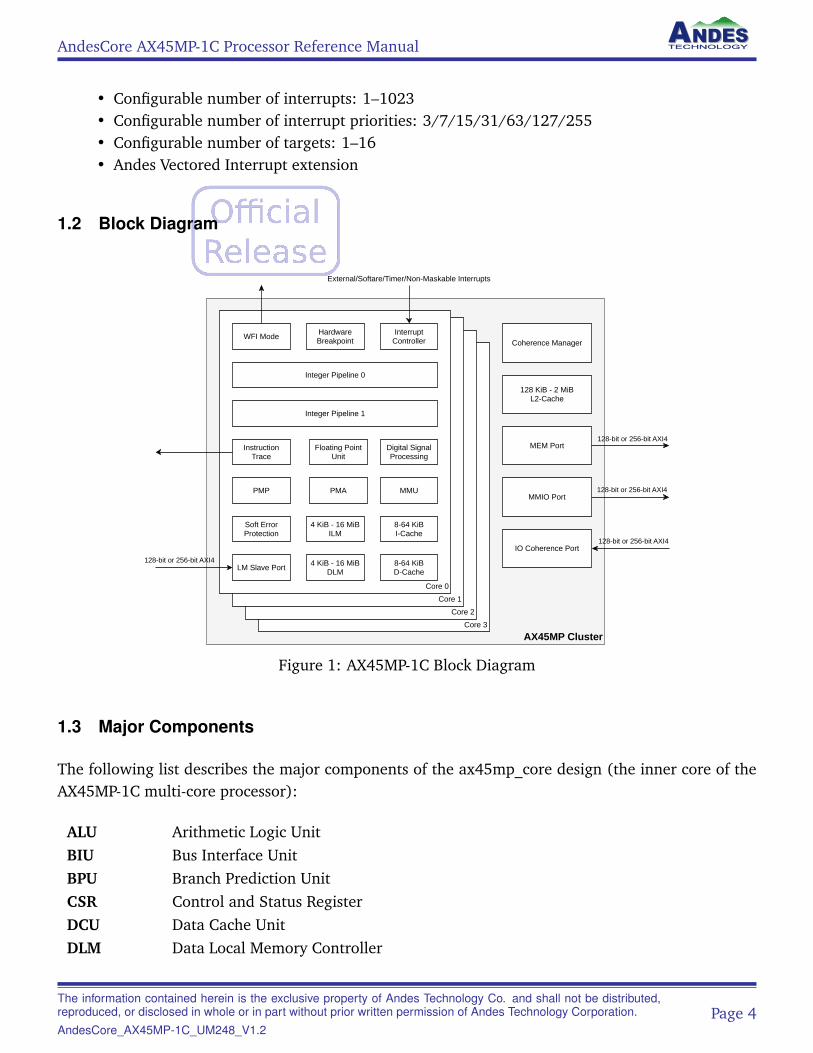
1.2 Block Diagram
AX45MP ClusterCore 3
Core 2
Core 1
Core 0
WFI ModeHardwareBreakpoint
InterruptController
Integer Pipeline 0
Integer Pipeline 1
InstructionTrace
Digital SignalProcessing
PMP
Soft ErrorProtection
8-64 KiBD-Cache
Coherence Manager
128 KiB - 2 MiBL2-Cache
MEM Port
MMIO Port
IO Coherence Port
128-bit or 256-bit AXI4
128-bit or 256-bit AXI4
128-bit or 256-bit AXI4
128-bit or 256-bit AXI4
4 KiB - 16 MiBDLM
4 KiB - 16 MiBILM
8-64 KiBI-Cache
PMA MMU
External/Softare/Timer/Non-Maskable Interrupts
Floating PointUnit
LM Slave Port
Figure 1: AX45MP-1C Block Diagram
1.3 Major Components
The following list describes the major components of the ax45mp_core design (the inner core of theAX45MP-1C multi-core processor):
ALU Arithmetic Logic UnitBIU Bus Interface UnitBPU Branch Prediction UnitCSR Control and Status RegisterDCU Data Cache UnitDLM Data Local Memory Controller
The information contained herein is the exclusive property of Andes Technology Co. and shall not be distributed,reproduced, or disclosed in whole or in part without prior written permission of Andes Technology Corporation.AndesCore_AX45MP-1C_UM248_V1.2
Page 4
AndesCore AX45MP-1C Processor Reference Manual
DSP Digital Signal ProcessingFASTMUL Fast MultiplierFPU Floating Point UnitICU Instruction Cache UnitIFU Instruction Fetch UnitILM Instruction Local Memory ControllerIPIPE Integer PipelineLSU Load Store UnitMDU Multiplication and Division UnitMMU Memory Manager UnitITLB Instruction Translation Lookaside BufferDTLB Data Translation Lookaside BufferPMA Programmable Physical Memory Attributes UnitPMP Physical Memory Protection UnitRF Integer Register FileTRIGM Trigger ModuleL2C Level-2 (L2) CacheCM Coherency ManagerIOCP I/O Coherency Port
1.4 Pipeline Stages and Activities
AX45MP-1C implements an 8-stage dual-issue pipeline architecture. The following figure shows thepipeline stages of the processor.
F1 F2 ID II EX MM LX WB
Fetch One Fetch Two Instruction
DecodeInstruction
IssueEarly
ExecutionData Memory
AccessLate
ExecutionInstruction Retire and
Result Writeback
The pipeline activities of the corresponding stages are:
F1—Instruction Fetch Stage 1
• Fetching an instruction block from ILM/Instruction cache/bus• Dynamic branch prediction
F2—Instruction Fetch Stage 2
• Fetch block data replies from ILM/Instruction cache/bus
The information contained herein is the exclusive property of Andes Technology Co. and shall not be distributed,reproduced, or disclosed in whole or in part without prior written permission of Andes Technology Corporation.AndesCore_AX45MP-1C_UM248_V1.2
Page 5
AndesCore AX45MP-1C Processor Reference Manual
• Branch prediction target acquired from BPU• Redirect fetch address to prediction target
ID—Instruction Decode
• Instruction decoding
II—Instruction Issue
• Instruction issue scheduling
EX—Early Execution
• Early ALU instruction execution
MM—Memory Access
• DLM/D-Cache access
LX—Late Execution
• Late ALU instruction execution
WB—Instruction Retire and Result Write-Back
• Interrupt resolution• Instruction retire• Register file write back
The information contained herein is the exclusive property of Andes Technology Co. and shall not be distributed,reproduced, or disclosed in whole or in part without prior written permission of Andes Technology Corporation.AndesCore_AX45MP-1C_UM248_V1.2
Page 6
AndesCore AX45MP-1C Processor Reference Manual
2 Instruction Set Overview
2.1 Introduction
AX45MP-1C implements The RISC-V Instruction Set Manual Volume I: Unprivileged ISA Document Ver-sion 20191213 (TD004). The following instruction sets are implemented:
• RV64I base integer instruction set
• RISC-V “C” standard extension
• RISC-V “M” standard extension
• RISC-V “A” standard extension
• RISC-V “F” and “D” standard extensions for single/double-precision floating-point
– FP16 half-precision floating-point extension
– Andes BFLOAT16 Extension
• RISC-V “P” extension for DSP/SIMD instructions
• AndeStar V5 instruction extension
For detailed information, please see The RISC-V Instruction Set Manual Volume I: Unprivileged ISADocument Version 20191213 (TD004) and AndeStar V5 Instruction Extension Specification (UM165).
2.2 Integer Registers
Table 1 lists all general-purpose integer registers.
Table 1: Integer Registers
Register Signal Name Description
x0 zero Hard-wired zero
x1 ra Return address
x2 sp Stack pointer
x3 gp Global pointer
x4 tp Thread pointer
x5 t0 Temporary/alternate link register
x6–x7 t1–t2 Temporaries
x8 s0/fp Saved register/frame pointer
Continued on next page. . .
The information contained herein is the exclusive property of Andes Technology Co. and shall not be distributed,reproduced, or disclosed in whole or in part without prior written permission of Andes Technology Corporation.AndesCore_AX45MP-1C_UM248_V1.2
Page 7
AndesCore AX45MP-1C Processor Reference Manual
Table 1: (continued)
Register Signal Name Description
x9 s1 Saved register
x10–x11 a0–a1 Function arguments/return values
x12–x17 a2–a7 Function arguments
x18–x27 s2–s11 Saved registers
x28–x31 t3–t6 Temporaries
2.3 Atomic Instructions
The RVA extension includes load-reserved/store-conditional and atomic memory operation (AMO)instructions.
2.3.1 Load-Reserved/Store-Conditional Instruction
The processor tracks at most one physical address location for LR-SC instructions at a time. Thereservation made by the LR instruction is canceled after any memory operation or exception happens.The address of SC instructions must match the reserved address for SC to succeed.
2.3.2 Atomic Memory Operation Instruction
An atomic memory operation is expanded to LR-modify-SC sequences in the processor. The mem-ory content is first loaded with the LR instruction, then the required operation is performed on theretrieved data, and the final result is written back to the memory by the SC instruction. If the SC
instruction fails, the sequence will be retried until it succeeds.
2.4 Misaligned Memory Access
AX45MP-1C implements the misaligned memory access to support accessing misaligned addresseswithout triggering any Address Misaligned exceptions.
By controlling the mmisc_ctl CSR, the scheme can be enabled or disabled. Please see Section 16.12.7for details.
The information contained herein is the exclusive property of Andes Technology Co. and shall not be distributed,reproduced, or disclosed in whole or in part without prior written permission of Andes Technology Corporation.AndesCore_AX45MP-1C_UM248_V1.2
Page 8
AndesCore AX45MP-1C Processor Reference Manual
2.4.1 Exceptions
When the misaligned memory access scheme is enabled, Access Fault exceptions will still be triggeredunder the following cases:
• Accesses to device regions• Accesses across ILM or DLM boundary• Accesses with inconsistency PMA attributes• Atomic accesses
If the misaligned memory access scheme is disabled, misaligned accesses will trigger Access Faultexceptions or Address Misaligned exceptions. Access fault exceptions are triggered when the followingcases occur:
• Atomic accesses• Address is located in a device region
Other misaligned accesses trigger Address Misaligned exceptions.
2.5 Floating-Point ISA Extension
AX45MP-1C supports the “F” and “D” Standard Extensions for accelerating the performance of floating-point heavy applications. The supported configuration is indicated in the misa (Machine ISA) con-figuration register.
AX45MP-1C supports the following FPU features:
• Fully pipelined MAC instructions• Hardware subnormal handling• All rounding modes
2.5.1 Support for Half-Precision and BFLOAT16 Formats
AX45MP-1C also supports instructions with half-precision (FP16) data type as well as Andes extensioninstructions for conversion between BFLOAT16 and single-precision formats.
The support for half-precision instructions are implemented by accepting the standard RISC-V floating-point instruction formats with the width field set to “H”.
The support for conversion instructions to/from BFLOAT16 are defined in the AndeStar V5 InstructionExtension Specification (UM165).
The information contained herein is the exclusive property of Andes Technology Co. and shall not be distributed,reproduced, or disclosed in whole or in part without prior written permission of Andes Technology Corporation.AndesCore_AX45MP-1C_UM248_V1.2
Page 9
AndesCore AX45MP-1C Processor Reference Manual
2.6 DSP ISA Extension
The processor implements the RISC-V “P” extension (draft) for DSP/SIMD ISA. The supported config-uration is indicated in the mmsc_cfg register. With the addition of the RISC-V “P” extension (draft),the processor can run various DSP applications with lower power and higher performance.
The supported DSP features include:
• SIMD Data Processing Instructions• Partial-SIMD Data Processing Instructions• 64-bit Profile Instructions• Non-SIMD Instructions• RV64 Only Instructions• Overflow Status Manipulation Instructions
Please see the AndeStar V5 DSP ISA Extension Specification (UM199) for instruction details.
The information contained herein is the exclusive property of Andes Technology Co. and shall not be distributed,reproduced, or disclosed in whole or in part without prior written permission of Andes Technology Corporation.AndesCore_AX45MP-1C_UM248_V1.2
Page 10
AndesCore AX45MP-1C Processor Reference Manual
3 Branch Prediction Unit
The processor implements Branch Prediction Unit (BPU) for branch prediction in instruction fetch.BPU contains a two-way 128-entry branch target buffer (BTB), a 4-entry return address stack (RAS),and a branch history table (BHT).
BTB is implemented to hold target addresses for unconditional jumps and conditional branches. RASis used to keep return addresses for function calls. BHT performs the taken/not taken prediction forthe conditional branches.
Branch predictions can be disabled by setting mmisc_ctl.BRPE to 0x0, which will make IFU fetchinstructions sequentially without predictions.
The information contained herein is the exclusive property of Andes Technology Co. and shall not be distributed,reproduced, or disclosed in whole or in part without prior written permission of Andes Technology Corporation.AndesCore_AX45MP-1C_UM248_V1.2
Page 11
AndesCore AX45MP-1C Processor Reference Manual
4 Memory Management Unit
4.1 Introduction
Memory Management Unit (MMU) is responsible for virtual address to physical address translation.The unit interfaces with the Instruction Fetch Control Unit (IFU) and the Load/Store Unit (LSU). AniTLB is implemented for IFU to speed up instruction address translation, while a dTLB is implementedfor LSU to speed up data address translation. If the address translation information is not availablein the iTLB or dTLB level, a TLB lookup request will be sent to Shared TLB (STLB), which is a biggerTLB defined in MMU. If a TLB miss happens in STLB, the hardware page table walker (PTW) willautomatically traverse through page tables for the translation information.
MMU needs to be enabled and be initialized before it can be used. The default state of MMU isdisabled which means there is no virtual to physical address translation. MMU is initialized throughthe satp CSR. Please see satp for details. Furthermore, SFENCE.VMA will be needed after satp isupdated.
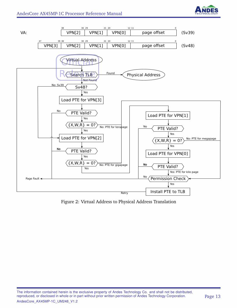
4.2 Address Translation
The virtual address to physical address translation is page based. For each virtual page, there is a pagetable entry (PTE) describing the physical page mapping information. Page table entries are insertedinto MMU (iTLB/dTLB/STLB) by the hardware page table walker (PTW) automatically.
The information contained herein is the exclusive property of Andes Technology Co. and shall not be distributed,reproduced, or disclosed in whole or in part without prior written permission of Andes Technology Corporation.AndesCore_AX45MP-1C_UM248_V1.2
Page 12
AndesCore AX45MP-1C Processor Reference Manual
Virtual Address
FoundSearch TLB
Load PTE for VPN[1]
PTE Valid?
{X,W,R} = 0?
Yes
No
Load PTE for VPN[0]
PTE Valid?
Permission Check
Yes: PTE for kilo page
No
Physical Address
Yes
No: PTE for megapage
Page Fault
No
No
Yes
Install PTE to TLBRetry
VA:
Not Found
Load PTE for VPN[3]
PTE Valid?
{X,W,R} = 0?
Yes
No
Load PTE for VPN[2]
PTE Valid?Yes
No
YesNo: PTE for terapage
No
{X,W,R} = 0?
Sv48?Yes
No: Sv39
VPN[1] VPN[0] page offsetVPN[2]VPN[3]
VPN[1] VPN[0] page offsetVPN[2]
(Sv48)39 38 30 29 21 20 12
38 30 29 21 20 12
47
11 0
11 0
(Sv39)
YesNo: PTE for gigapage
Figure 2: Virtual Address to Physical Address Translation
The information contained herein is the exclusive property of Andes Technology Co. and shall not be distributed,reproduced, or disclosed in whole or in part without prior written permission of Andes Technology Corporation.AndesCore_AX45MP-1C_UM248_V1.2
Page 13
AndesCore AX45MP-1C Processor Reference Manual
4.3 Translation Lookaside Buffer
The following sections describe the TLB operations.
4.3.1 Instruction uTLB (iTLB)
Instruction uTLB(iTLB) is a 4/8-entry fully-associative cache that stores address translations (i.e., thePage Table Entries, PTEs) for instruction fetches. The iTLB gets the translation information from STLBunder iTLB misses. SFENCE.VMA operations or write to satp will clear all non-global entries in iTLB.
4.3.2 Data uTLB (dTLB)
Data uTLB(dTLB) is a 4/8-entry fully-associative cache that stores address translations (i.e., the PageTable Entries, PTEs) for data accesses. dTLB gets the translation information from STLB under dTLBmisses. SFENCE.VMA operations write to satp will clear all non-global entries in dTLB.
4.3.3 Shared TLB (STLB)
The Shared TLB (STLB) contains a 32/64/128/256/512-entry 4-way set-associative structure for 4Kpages and a 4-entry fully-associative structure for superpages that store address translations (i.e., thePage Table Entries, PTEs) for both instruction fetches and data accesses.
4.3.4 Replacement Policy
TLBs (iTLB/dTLB/STLB) all implement pseudo-LRU replacement policy.
4.4 Page Table Walker (PTW)
4.4.1 Introduction
The page table walker is responsible for automatically filling STLB with PTE entries located in thesystem memory when there is a STLB lookup miss. Each TLB miss will require two to four memoryreferences. The implementation caches non-leaf PTEs to speed up page table hierarchy traversal. Twosets of non-leaf PTE caches are implemented—one for misses originating from instruction fetches andthe other one for misses originating from data loads/stores.
The information contained herein is the exclusive property of Andes Technology Co. and shall not be distributed,reproduced, or disclosed in whole or in part without prior written permission of Andes Technology Corporation.AndesCore_AX45MP-1C_UM248_V1.2
Page 14
AndesCore AX45MP-1C Processor Reference Manual
4.4.2 Page Table Address Formation
To find the correct PTE from the page table in memory, the PTW needs to perform up to three or fourmemory read operations to get PTEs. The physical addresses for these read operations are formed bythe PTW as follows:
1. Let a be satp.ppn × PAGESIZE, and let i = LEVELS - 1. (PAGESIZE=212 and for Sv39, LEV-ELS=3; for Sv48, LEVELS=4.)
2. The physical address for PTE of VPN[i] is a + va.vpn[i] × 8. Perform a memory read to retrievethe PTE at this location. PMP checks are also applicable to memory reads accessing the PTEs. Ifa violation occurs, an access exception will be raised based on the access type of the instructionstriggering this page table walk. Let pte be the value of the memory read if no access violationoccurs.
3. If pte.v = 0, or if (w, r) of pte is (1, 0), stop and raise a page-fault exception based on the accesstype of the instructions triggering this page table walk.
4. Otherwise, the PTE is valid.
• If (x, w, r) of pte is (0, 0, 0), this PTE is a pointer to the next level of the page table. Let i = i -1, a = pte.ppn × PAGESIZE and go to step 2 unless i < 0, in which case a page-fault exceptionshould be raised based on the access type of the instructions triggering this page table walk.
• If (x, w, r) of pte is not (0, 0, 0), then the leaf PTE for the page is found.
4.5 Attributes for Address Spaces
4.5.1 Attributes for Virtual Memory Pages
Each memory page is associated with attributes controlling page accesses. These attributes are storedin the page table entries along with their physical address mappings. The following table describesthe format for the page table entries.
X W R Meaning
0 0 0 Pointer to next level of page table
0 0 1 Read-only page
0 1 0 Reserved for future use
0 1 1 Read-write page
1 0 0 Execute-only page
1 0 1 Read-execute page
Continued on next page. . .
The information contained herein is the exclusive property of Andes Technology Co. and shall not be distributed,reproduced, or disclosed in whole or in part without prior written permission of Andes Technology Corporation.AndesCore_AX45MP-1C_UM248_V1.2
Page 15
AndesCore AX45MP-1C Processor Reference Manual
X W R Meaning
1 1 0 Reserved for future use
1 1 1 Read-write-execute page
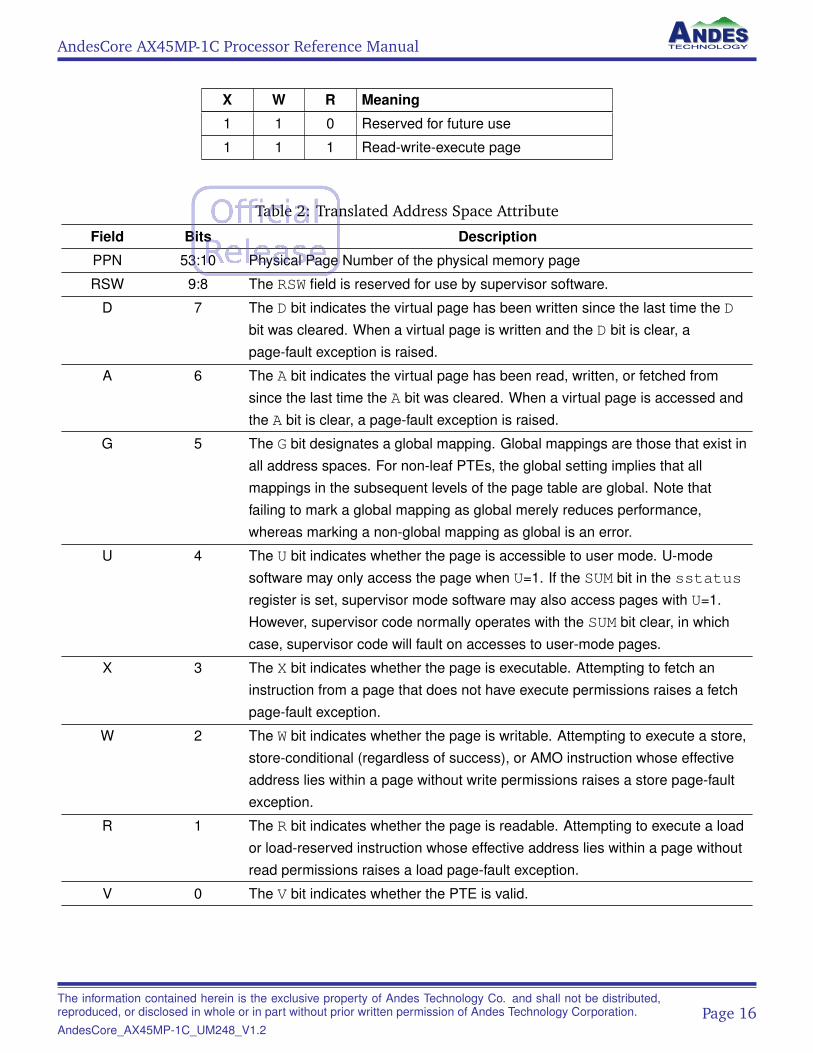
Table 2: Translated Address Space Attribute
Field Bits Description
PPN 53:10 Physical Page Number of the physical memory page
RSW 9:8 The RSW field is reserved for use by supervisor software.
D 7 The D bit indicates the virtual page has been written since the last time the Dbit was cleared. When a virtual page is written and the D bit is clear, apage-fault exception is raised.
A 6 The A bit indicates the virtual page has been read, written, or fetched fromsince the last time the A bit was cleared. When a virtual page is accessed andthe A bit is clear, a page-fault exception is raised.
G 5 The G bit designates a global mapping. Global mappings are those that exist inall address spaces. For non-leaf PTEs, the global setting implies that allmappings in the subsequent levels of the page table are global. Note thatfailing to mark a global mapping as global merely reduces performance,whereas marking a non-global mapping as global is an error.
U 4 The U bit indicates whether the page is accessible to user mode. U-modesoftware may only access the page when U=1. If the SUM bit in the sstatusregister is set, supervisor mode software may also access pages with U=1.However, supervisor code normally operates with the SUM bit clear, in whichcase, supervisor code will fault on accesses to user-mode pages.
X 3 The X bit indicates whether the page is executable. Attempting to fetch aninstruction from a page that does not have execute permissions raises a fetchpage-fault exception.
W 2 The W bit indicates whether the page is writable. Attempting to execute a store,store-conditional (regardless of success), or AMO instruction whose effectiveaddress lies within a page without write permissions raises a store page-faultexception.
R 1 The R bit indicates whether the page is readable. Attempting to execute a loador load-reserved instruction whose effective address lies within a page withoutread permissions raises a load page-fault exception.
V 0 The V bit indicates whether the PTE is valid.
The information contained herein is the exclusive property of Andes Technology Co. and shall not be distributed,reproduced, or disclosed in whole or in part without prior written permission of Andes Technology Corporation.AndesCore_AX45MP-1C_UM248_V1.2
Page 16
AndesCore AX45MP-1C Processor Reference Manual
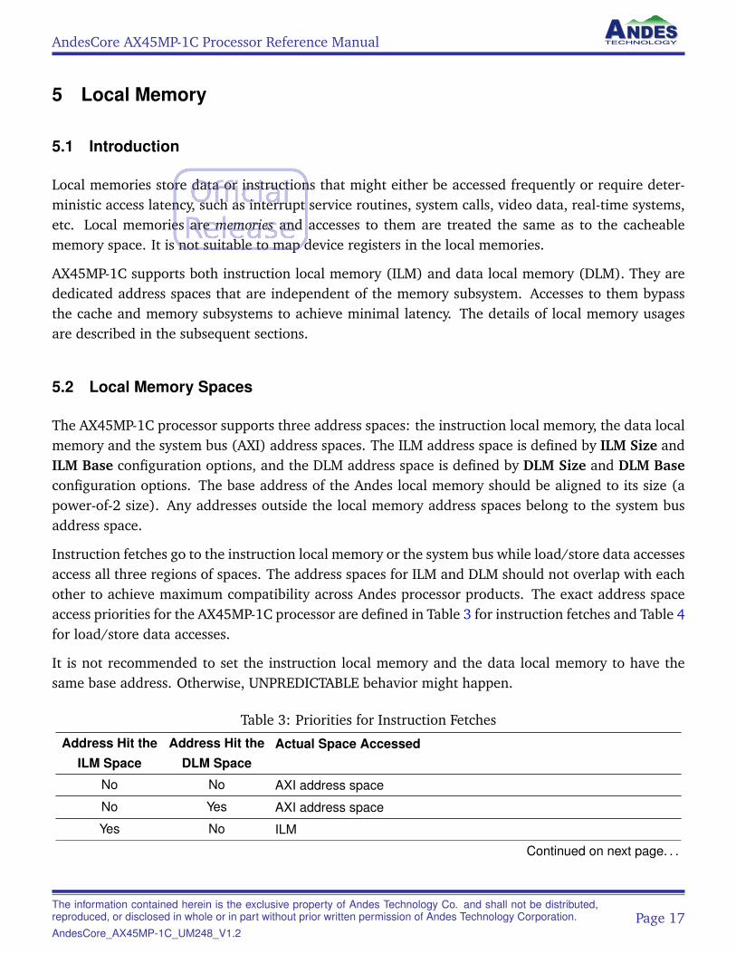
5 Local Memory
5.1 Introduction
Local memories store data or instructions that might either be accessed frequently or require deter-ministic access latency, such as interrupt service routines, system calls, video data, real-time systems,etc. Local memories are memories and accesses to them are treated the same as to the cacheablememory space. It is not suitable to map device registers in the local memories.
AX45MP-1C supports both instruction local memory (ILM) and data local memory (DLM). They arededicated address spaces that are independent of the memory subsystem. Accesses to them bypassthe cache and memory subsystems to achieve minimal latency. The details of local memory usagesare described in the subsequent sections.
5.2 Local Memory Spaces
The AX45MP-1C processor supports three address spaces: the instruction local memory, the data localmemory and the system bus (AXI) address spaces. The ILM address space is defined by ILM Size andILM Base configuration options, and the DLM address space is defined by DLM Size and DLM Baseconfiguration options. The base address of the Andes local memory should be aligned to its size (apower-of-2 size). Any addresses outside the local memory address spaces belong to the system busaddress space.
Instruction fetches go to the instruction local memory or the system bus while load/store data accessesaccess all three regions of spaces. The address spaces for ILM and DLM should not overlap with eachother to achieve maximum compatibility across Andes processor products. The exact address spaceaccess priorities for the AX45MP-1C processor are defined in Table 3 for instruction fetches and Table 4for load/store data accesses.
It is not recommended to set the instruction local memory and the data local memory to have thesame base address. Otherwise, UNPREDICTABLE behavior might happen.
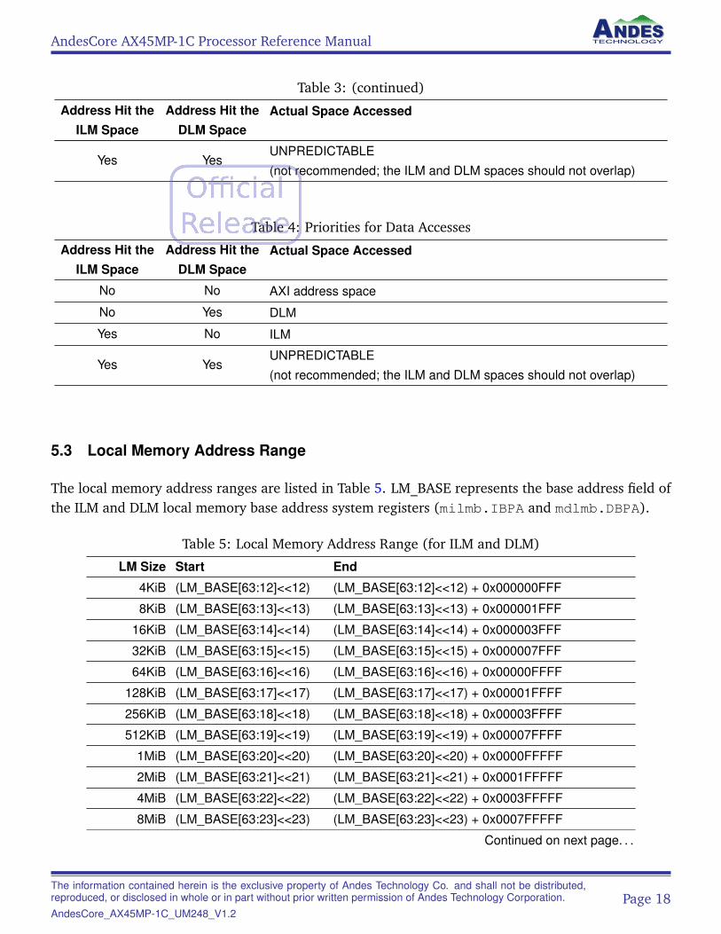
Table 3: Priorities for Instruction Fetches
Address Hit theILM Space
Address Hit theDLM Space
Actual Space Accessed
No No AXI address space
No Yes AXI address space
Yes No ILM
Continued on next page. . .
The information contained herein is the exclusive property of Andes Technology Co. and shall not be distributed,reproduced, or disclosed in whole or in part without prior written permission of Andes Technology Corporation.AndesCore_AX45MP-1C_UM248_V1.2
Page 17
AndesCore AX45MP-1C Processor Reference Manual
Table 3: (continued)
Address Hit theILM Space
Address Hit theDLM Space
Actual Space Accessed
Yes YesUNPREDICTABLE(not recommended; the ILM and DLM spaces should not overlap)
Table 4: Priorities for Data Accesses
Address Hit theILM Space
Address Hit theDLM Space
Actual Space Accessed
No No AXI address space
No Yes DLM
Yes No ILM
Yes YesUNPREDICTABLE(not recommended; the ILM and DLM spaces should not overlap)
5.3 Local Memory Address Range
The local memory address ranges are listed in Table 5. LM_BASE represents the base address field ofthe ILM and DLM local memory base address system registers (milmb.IBPA and mdlmb.DBPA).
Table 5: Local Memory Address Range (for ILM and DLM)
LM Size Start End
4KiB (LM_BASE[63:12]<<12) (LM_BASE[63:12]<<12) + 0x000000FFF
8KiB (LM_BASE[63:13]<<13) (LM_BASE[63:13]<<13) + 0x000001FFF
16KiB (LM_BASE[63:14]<<14) (LM_BASE[63:14]<<14) + 0x000003FFF
32KiB (LM_BASE[63:15]<<15) (LM_BASE[63:15]<<15) + 0x000007FFF
64KiB (LM_BASE[63:16]<<16) (LM_BASE[63:16]<<16) + 0x00000FFFF
128KiB (LM_BASE[63:17]<<17) (LM_BASE[63:17]<<17) + 0x00001FFFF
256KiB (LM_BASE[63:18]<<18) (LM_BASE[63:18]<<18) + 0x00003FFFF
512KiB (LM_BASE[63:19]<<19) (LM_BASE[63:19]<<19) + 0x00007FFFF
1MiB (LM_BASE[63:20]<<20) (LM_BASE[63:20]<<20) + 0x0000FFFFF
2MiB (LM_BASE[63:21]<<21) (LM_BASE[63:21]<<21) + 0x0001FFFFF
4MiB (LM_BASE[63:22]<<22) (LM_BASE[63:22]<<22) + 0x0003FFFFF
8MiB (LM_BASE[63:23]<<23) (LM_BASE[63:23]<<23) + 0x0007FFFFF
Continued on next page. . .
The information contained herein is the exclusive property of Andes Technology Co. and shall not be distributed,reproduced, or disclosed in whole or in part without prior written permission of Andes Technology Corporation.AndesCore_AX45MP-1C_UM248_V1.2
Page 18
AndesCore AX45MP-1C Processor Reference Manual
Table 5: (continued)
LM Size Start End
16MiB (LM_BASE[63:24]<<24) (LM_BASE[63:24]<<24) + 0x000FFFFFF
5.4 Local Memory Usage Constraints
Local memories are optimized for access latency. As a result, the design imposes the following usagerestrictions:
• Offset addresses of VA and PA should be the same for the part of address offsets that address offsetmappings for the offset part of the address that indexes into the local memory.
• Accesses to the local memory are speculative. Devices with side effects on reads should not bemapped to this region.
The information contained herein is the exclusive property of Andes Technology Co. and shall not be distributed,reproduced, or disclosed in whole or in part without prior written permission of Andes Technology Corporation.AndesCore_AX45MP-1C_UM248_V1.2
Page 19
AndesCore AX45MP-1C Processor Reference Manual
6 Local Memory Slave Port
6.1 Introduction
The LM slave port enables external bus masters to access the local memories of each core.
When an address exceeds ILM/DLM size, the higher address bits are ignored by the slave port.
The LM slave port supports FIXED, INCR, and WRAP of AXI burst type and contains five channel FIFOsfor read and write accesses. Therefore, all transfers might temporarily be stored in the FIFOs and around-robin arbiter is used to schedule the read/write access.
Note that AX45MP-1C does not include logics to guarantee atomicity of atomic instructions accessingthe LM address space when external masters access the same location through the LM slave port, nordoes it provide the protection feature on LM slave port.
6.2 Support for Soft Error Protection
The LM slave port would return bus errors to AXI masters as well as trigger local interrupts to AX45MP-1C when a 2-bit ECC error is detected.
The behavior of ECC logic for local memories is controlled by milmb.ECCEN/mdlmb.ECCEN. Theencoding for errors encountered through accesses from the LM slave port is summarized in the tablebelow.
Correctable ECC errors only trigger local interrupts when ECCEN is equal to 3. Uncorrectable ECCerrors would trigger local interrupts when ECCEN is equal to 2 or 3. The triggering of local interruptsis controlled by mie.IMECCI and the interrupt status is reported in mip.IMECCI. See Section 16.3.5and Section 16.3.11 for details.
Data returned through the LM slave port is the ECC corrected version. For uncorrectable ECC errors,bus errors are reported when ECCEN is equal to 2 or 3.
ECCEN Meaning Data Returned
0 Disable parity/ECC Uncorrected data
1 Reserved Reserved
2 Generate local interrupts only onuncorrectable parity/ECC errors
Corrected data or bus errors
3 Generate local interrupts on any type ofparity/ECC errors
Corrected data or bus errors
The information contained herein is the exclusive property of Andes Technology Co. and shall not be distributed,reproduced, or disclosed in whole or in part without prior written permission of Andes Technology Corporation.AndesCore_AX45MP-1C_UM248_V1.2
Page 20
AndesCore AX45MP-1C Processor Reference Manual
7 Level-1 Caches
7.1 Introduction
AX45MP-1C contains two Level-1 (L1) caches, the instruction cache and the data cache. Both can beconfigured to 8KiB, 16KiB, 32KiB, or 64KiB in size. The cache line size is fixed to 64 bytes.
The cache organization information can be collected from the micm_cfg register for the instructioncache and the mdcm_cfg register for the data cache. The configuration choices are listed below, andthe format of the configuration registers can be found in Section 16.5.1 and Section 16.5.2.
Table 6: Configuration Choices for the I-Cache
I-Cache Size Ways(micm_cfg.IWAY)
Cache lines perway (micm_cfg.ISET)
8 KiB 1 128
2 64
4 32
16 KiB 1 256
2 128
4 64
32 KiB 1 512
2 256
4 128
64 KiB 1 1024
2 512
4 256
Table 7: Configuration Choices for the D-Cache
D-Cache Size Ways(mdcm_cfg.DWAY)
Cache lines perway (mdcm_cfg.DSET)
8 KiB 1 128
2 64
4 32
Continued on next page. . .
The information contained herein is the exclusive property of Andes Technology Co. and shall not be distributed,reproduced, or disclosed in whole or in part without prior written permission of Andes Technology Corporation.AndesCore_AX45MP-1C_UM248_V1.2
Page 21
AndesCore AX45MP-1C Processor Reference Manual
Table 7: (continued)
D-Cache Size Ways(mdcm_cfg.DWAY)
Cache lines perway (mdcm_cfg.DSET)
16 KiB 1 256
2 128
4 64
32 KiB 1 512
2 256
4 128
64 KiB 1 1024
2 512
4 256
7.2 Cache Replacement Policy
The replacement policy for direct-mapped caches is irrelevant. 2-way and 4-way caches implementrandom or tree pseudo-LRU replacement policy.
7.3 I-Cache
I-Cache is virtually indexed and physically tagged (VIPT).
7.3.1 I-Cache Fill Operation
The instruction cache fill operation starts when a cacheable line is not in the I-Cache. After a cachemiss, a burst read request for the missed cache line is issued to system bus to reduce access time forthe missed cache line data. Up to two outstanding requests can be issued to system bus.
The fill operation may be aborted by system bus errors. A precise instruction access fault is triggeredfor the instruction fetch causing the cache miss operation if the error is on the critical word. If theerror occurs on non-critical words, the fill operation will be canceled and the missed line will not beinstalled into I-Cache. Instruction fetches before non-critical error words will not be affected sincethey have received the required data.
In Debug Mode, instruction fetches will not affect I-Cache contents, and all I-Cache misses will notcause cache replacements.
The information contained herein is the exclusive property of Andes Technology Co. and shall not be distributed,reproduced, or disclosed in whole or in part without prior written permission of Andes Technology Corporation.AndesCore_AX45MP-1C_UM248_V1.2
Page 22
AndesCore AX45MP-1C Processor Reference Manual
7.3.2 I-Cache Prefetch
After cache miss, a series of sequential cache lines will be probed to check whether they are in I-Cache.If not, streaming prefetch will be performed for these sequential cache lines. The instruction prefetchis turned off by default, and can be turned on by setting mcache_ctl.IPREF_EN to 0x1.
7.3.3 I-Cache TAG SRAM Fields
Table 8: I-Cache TAG SRAM Fields
Field Bit Position Description
TAG [0+:ICACHE_TAG_WIDTH] TAG
LOCK_DUP [ICACHE_TAG_WIDTH] Duplicated lock bit for error protection
LOCK [ICACHE_TAG_WIDTH+1] Indicate the line is locked
VALID [ICACHE_TAG_WIDTH+2] Indicate the line is valid
NoteICACHE_TAG_WIDTH = BIU_ADDR_WIDTH - min(12, (6 + log2(micm_cfg.ISET))
The information contained herein is the exclusive property of Andes Technology Co. and shall not be distributed,reproduced, or disclosed in whole or in part without prior written permission of Andes Technology Corporation.AndesCore_AX45MP-1C_UM248_V1.2
Page 23
AndesCore AX45MP-1C Processor Reference Manual
7.4 D-Cache
D-Cache is physically indexed and physically tagged (PIPT).
7.4.1 Cache Access Latency
Table 9: Access Latency of the D-Cache
Condition Load-to-Use Latency (Cycles)
D-Cache Hit 0
Modified line in another core 57
L2-Cache hit 24
L2-Cache miss 27
Note• The latency assumes that load word instructions are used to access D-Cache.• The latency assumes that bus latency is one cycle after the request address is issued.• The latency assumes that the dependent instruction is executed in late ALU.• The latency assumes that the miss address is the first transfer of a cache line.• The 0-cycle latency assumes that the dependent instruction and the load instruction are dual-issued.• The latency assumes that the CORE_CLK and BUS_CLK clock ratio is 1:1.• The latency assumes that the latency of memory access is 1 cycle.• The latency assumes that the bus data width is 128-bit.• The latency assumes that Tag RAM output cycle of L2-Cache is 1 cycle.• The latency assumes that Tag RAM setup cycle of L2-Cache is 1 cycle.• The latency assumes that Data RAM output cycle of L2-Cache is 1 cycle.• The latency assumes that Data RAM setup cycle of L2-Cache is 1 cycle.
7.4.2 D-Cache Fill Operations
The D-Cache fill operation starts when a cacheable line is not in the D-Cache. A burst read requestfor the missed cache line is always sent first to the system bus to minimize the miss latency. The readrequest will be followed by a burst write request if cache eviction is required.
The information contained herein is the exclusive property of Andes Technology Co. and shall not be distributed,reproduced, or disclosed in whole or in part without prior written permission of Andes Technology Corporation.AndesCore_AX45MP-1C_UM248_V1.2
Page 24
AndesCore AX45MP-1C Processor Reference Manual
The fill operation may be aborted by system bus errors. A precise load access fault is triggered forthe load instruction causing the cache miss operation if the bus error is for the critical word. The buserror on non-critical words does not trigger an exception, but the fill operation will be canceled andthe missed line will not be installed into D-Cache. Store is always non-blocking. Bus errors on storecache miss will trigger bus-write transaction errors.
System bus errors will no longer be reported as precise exceptions if the processor is in the non-blocking mode (mmisc_ctl.NBLD_EN). Bus Read/Write Transaction Error Local Interrupts (mip.BWEI) will be reported instead. Please see Section 11.1 for details.
In Debug Mode, load/store instructions will minimally affect D-Cache contents. All cache misses willnot cause cache replacements, and only dirty bits may be affected by accesses to cache lines that arealready in D-Cache.
7.4.3 D-Cache Eviction Operations
A burst write request will be sent to L2 if a dirty line is evicted out of D-Cache. An imprecise bus-writeerror exception is triggered if the burst write request encounters system bus errors.
7.4.4 D-Cache Write Buffers
D-Cache implements two write buffers, and each buffer is used to buffer a 64-byte line. When D-Cache evicts a line, the evicted line is temporarily buffered in one of the write buffers and then sendto L2 from that write buffer.
When the Write-Around feature is configured, store to write-no-allocate memory is also buffered inone of the write buffers. Multiple stores can be merged into a single transaction. The buffered line isflushed in any of the following conditions:
• The line is completely filled by subsequent store operations.• A store operation writes to another line in write-no-allocate memory.• A load operation accesses the buffered line.• A FENCE, FENCE.I, or SFENCE.VMA instruction is under execution.• A CCTL operation is under execution.• The processor is in debug mode.• The processor is WFI mode.• D-Cache is disabled (mcache_ctl.DC_EN is cleared).
Write-no-allocate memory consists of:
• A D-Cache miss, which occurs for a store operation when D-Cache is in the write-no-allocate mode(See Section 11.2).
The information contained herein is the exclusive property of Andes Technology Co. and shall not be distributed,reproduced, or disclosed in whole or in part without prior written permission of Andes Technology Corporation.AndesCore_AX45MP-1C_UM248_V1.2
Page 25
AndesCore AX45MP-1C Processor Reference Manual
• PMA of the memory, which is set as (Memory, Write-back, No-allocate/Read-allocate) (MTYP=8/9).
NoteWhen the Write-Around feature is not configured, store to write-no-allocate memory is not buffered.
7.4.5 D-Cache TAG SRAM Fields
Table 10: D-Cache TAG SRAM Fields
Field Bit Position Description
MESI [2:0] Indicate cache line states.
Value Meaning
000 Invalid. The line is not inD-Cache.
001 Shared. The line is clean,and is shared by multiplecaches.
011 Exclusive. The cache lineis present only in thecurrent cache, but is clean.
111 Modified. The line ispresent only in the currentcache, and is dirty.
LOCK [3] Indicate the line is locked
TAG [4+:DCACHE_TAG_WIDTH)] TAG
NoteDCACHE_TAG_WIDTH = BIU_ADDR_WIDTH - 6 - log2(mdcm_cfg.DSET)
The information contained herein is the exclusive property of Andes Technology Co. and shall not be distributed,reproduced, or disclosed in whole or in part without prior written permission of Andes Technology Corporation.AndesCore_AX45MP-1C_UM248_V1.2
Page 26
AndesCore AX45MP-1C Processor Reference Manual
7.5 FENCE/FENCE.I Operations
FENCE/FENCE.I instructions may affect caches when caches are enabled. If mcache_ctl.IC_ENis 0, FENCE.I instructions will not perform any operation on the I-Cache. If mcache_ctl.DC_EN is0, FENCE.I instructions will not perform any operation on the D-Cache. FENCE instructions do notperform any operation on either I-Cache or D-Cache. The behavior of FENCE/FENCE.I is summarizedin Table 11.
Table 11: Effects of FENCE/FENCE.I Instructions
Cache FENCE FENCE.I
I-Cache None Invalidate all cache lines
D-Cache None Write back all cache lines
7.6 CCTL Operations
CCTL operations provide direct control to manipulate instruction or data caches (cache maintenanceoperations). They are invoked by writing CCTL commands to the mcctlcommand CSR register. Theoperations can be grouped into two main types, virtual-address (VA) based or index (IX) based, andthey are summarized in Table 12. These two addressing types affect how cache lines are specified forCCTL operations, and how the content of mcctlbeginaddr are interpreted.
Table 12: Addressing Type of CCTL Commands
Type Usage
IX Use the content of mcctlbeginaddr register directly as a (Way, Index) or (Way,Index, Double-Word/word) pair/tuple to specify a cache line in the cache withoutgoing through any translation mechanism. The format is defined in Table 13 andTable 14.
VA Use the content of mcctlbeginaddr register as a virtual address to access thecache. The virtual address has to go through the same address translationmechanism in the processor pipeline as the address of regular load/storeinstructions for D-Cache or instruction fetches for I-Cache. The specified operation isperformed only if the addressed cache line is in the corresponding cache.
The information contained herein is the exclusive property of Andes Technology Co. and shall not be distributed,reproduced, or disclosed in whole or in part without prior written permission of Andes Technology Corporation.AndesCore_AX45MP-1C_UM248_V1.2
Page 27
AndesCore AX45MP-1C Processor Reference Manual
Table 13: Index Format for D-Cache Index Type of CCTL Operations
Field Bit Position Description
OFFSET mcctlbeginaddr[A-1:3] A=log2(#Double-Words in a Cache Line) + 3
INDEX mcctlbeginaddr[B-1:A] B=log2(Cache Size / #Ways)
WAY mcctlbeginaddr[C-1:B] C=Ceiling(log2(Cache Size))
Table 14: Index Format for I-Cache Index Type of CCTL Operations
Field Bit Position Description
OFFSET mcctlbeginaddr[A-1:2] A=log2(#Words in a Cache Line) + 2
INDEX mcctlbeginaddr[B-1:A] B=log2(Cache Size / #Ways)
WAY mcctlbeginaddr[C-1:B] C=Ceiling(log2(Cache Size))
The following diagram shows an example of mcctlbeginaddr for the index type of CCTL opera-tions, assuming that cache is 4-way, 32-KiB with 64-byte cache line for D-Cache.
63 15
0
14 13
WAY
12 6
INDEX
5 3
OFFSET
2 0
0
The following diagram shows an example of mcctlbeginaddr for the index type of CCTL opera-tions, assuming that cache is 4-way, 32-KiB with 64-byte cache line for I-Cache.
63 15
0
14 13
WAY
12 6
INDEX
5 2
OFFSET
1 0
0
All available CCTL operations are summarized in Table 58. Their detailed definitions are grouped anddescribed in the following categories.
7.6.1 Invalidating Cache Blocks (L1D_VA_INVAL, L1I_VA_INVAL, L1D_IX_INVAL, L1I_IX_INVAL)
These operations invalidate the specified cache lines. Locked cache lines are unlocked and invalidated.
7.6.2 Writing Back Cache Blocks (L1D_VA_WB, L1D_IX_WB, L1D_WB_ALL)
These operations write the data of the specified cache lines back to the system memory, if the specifiedcache lines are present in the cache with dirty states. The specified cache lines will still be kept in thecache and locked cache lines remain locked.
The information contained herein is the exclusive property of Andes Technology Co. and shall not be distributed,reproduced, or disclosed in whole or in part without prior written permission of Andes Technology Corporation.AndesCore_AX45MP-1C_UM248_V1.2
Page 28
AndesCore AX45MP-1C Processor Reference Manual
7.6.3 Writing Back & Invalidating Cache Blocks (L1D_VA_WBINVAL, L1D_IX_WBINVAL, L1D_WBIN-VAL_ALL)
These operations write the data of the specified cache lines back to the system memory, if the specifiedcache lines are present in the cache with dirty states. Then the specified cache lines will be invalidatedas long as they are valid in the cache, regardless of whether their states are dirty or locked.
7.6.4 Filling and Locking Cache Blocks (L1D_VA_LOCK, L1I_VA_LOCK)
These operations lock the specified cache lines in the cache. The specified cache lines are first broughtinto the cache if they are not already present in the cache, then the cache lines are locked by settingtheir lock states. It is not an error to lock an already locked line—the same line is just locked again.
The lock state only affects the cache replacement policy. On cache miss, an unlocked lines will bereplaced first. When all ways are locked, the missed line is not allocated in the cache.
The status of lock operations are written to the mcctldata register:
• A value of 1 indicates that the lock operation finished successfully;
• A value of 0 indicates that the lock operation aborted/failed.
– locking an address in device or non-cacheable memory
– locking an address in local memory (ILM/DLM)
– locking an line when all ways are locked, and the line is not present in the cache
7.6.5 Unlocking Cache Blocks (L1D_VA_UNLOCK, L1I_VA_UNLOCK)
These operations clear the lock state of the specified cache lines if the specified cache lines are presentin the cache.
7.6.6 Reading Tag Data from Caches (L1D_IX_RTAG, L1I_IX_RTAG)
These operations read the contents of the tag part of the target cache line into the mcctldata
register. The format of the tag data in mcctldata is defined in Section 16.12.11. The target cacheline is specified in the mcctlbeginaddr register by its way and index information. Additionally,these operations observe DC_RWECC/IC_RWECC settings in mcache_ctl to read the correspondingECC/Parity codes in the tag RAM to mecc_code.
The information contained herein is the exclusive property of Andes Technology Co. and shall not be distributed,reproduced, or disclosed in whole or in part without prior written permission of Andes Technology Corporation.AndesCore_AX45MP-1C_UM248_V1.2
Page 29
AndesCore AX45MP-1C Processor Reference Manual
7.6.7 Reading Data from D-Cache (L1D_IX_RDATA)
This operation reads an 8-byte data from a cache line into the mcctldata register. The target cacheline is specified in the mcctlbeginaddr register by its way, index, and double word information.Additionally, this operation observes DC_RWECC settings in mcache_ctl to read the correspondingECC codes in the data RAM to mecc_code.
7.6.8 Reading Data from I-Caches (L1I_IX_RDATA)
This operation reads a 4-byte data from a cache line into the mcctldata register. The target cacheline is specified in the mcctlbeginaddr register by its way, index, and word information. Addi-tionally, this operation observes IC_RWECC settings in mcache_ctl to read the corresponding Paritycodes in the data RAM to mecc_code.
7.6.9 Writing Tag Data to Caches (L1D_IX_WTAG, L1I_IX_WTAG)
These operations write the contents of the mcctldata register to the tag part of the target cacheline. The format of the tag data in mcctldata is defined in Section 16.12.11. The target cacheline is specified in the mcctlbeginaddr register by its way and index information. Additionally,these operations observe DC_RWECC/IC_RWECC settings in mcache_ctl to write the mecc_codeECC/Parity code to the corresponding tag RAM.
NoteWriting unexpected Tag data to a cache might lead to UNPREDICTABLE behavior when the cache is enable.It is recommended to clear TAG SRAM before enabling the cache.
7.6.10 Writing Data to D-Cache (L1D_IX_WDATA)
This operation writes an 8-byte data in the mcctldata register into the target cache line. Thetarget cache line is specified in the mcctlbeginaddr register by its way, index, and double wordinformation. Additionally, this operation observes DC_RWECC settings in mcache_ctl to write themecc_code ECC code to the corresponding data RAM.
The information contained herein is the exclusive property of Andes Technology Co. and shall not be distributed,reproduced, or disclosed in whole or in part without prior written permission of Andes Technology Corporation.AndesCore_AX45MP-1C_UM248_V1.2
Page 30
AndesCore AX45MP-1C Processor Reference Manual
7.6.11 Writing Data to I-Caches (L1I_IX_WDATA)
This operation writes a 4-byte data in the mcctldata register into the target cache line. The targetcache line is specified in the mcctlbeginaddr register by its way, index, and word information.Additionally, this operation observes IC_RWECC settings in mcache_ctl to write the mecc_code
Parity code to the corresponding data RAM.
7.6.12 Invalidating All Cache Blocks (L1D_INVAL_ALL)
This operation invalidates all valid lines of D-Cache. Locked cache lines are unlocked and invalidated.
7.6.13 Writing Back All Cache Blocks (L1D_WB_ALL)
This operation writes the data of all dirty cache lines of D-Cache back to the system memory. All cachelines will still remain in the D-Cache and locked lines remain locked.
7.6.14 Writing Back & Invalidating All Cache Blocks (L1D_WBINVAL_ALL)
This operation writes the data of all dirty cache lines of D-Cache back to the system memory and allvalid cache lines will be invalidated, including locked and/or clean cache lines.
7.7 Supervisor/User CCTL Operations
CCTL operations are available to Supervisor/User-mode software under the control of the mcache_ctl.CCTL_SUEN control bit. These operations are triggered in both modes by accessing ucctlbeginaddr, ucctlcommand and scctldata registers, while mcache_ctl.CCTL_SUEN controls accesspermission to these registers. When CCTL_SUEN is 0, accessing them in Supervisor and User modewould cause illegal instruction exceptions. It should be set to 1 to enable Supervisor (and User) CCTLoperations.
All CCTL operations can be made available to Supervisor-mode software while only four CCTL oper-ations listed in the table below are available to User-mode software.
Table 15: User CCTL Operations
Value Command Type Exception Entry
0 0b00_000 L1D_VA_INVAL VA Store related Fault
1 0b00_001 L1D_VA_WB VA Store related Fault
Continued on next page. . .
The information contained herein is the exclusive property of Andes Technology Co. and shall not be distributed,reproduced, or disclosed in whole or in part without prior written permission of Andes Technology Corporation.AndesCore_AX45MP-1C_UM248_V1.2
Page 31
AndesCore AX45MP-1C Processor Reference Manual
Table 15: (continued)
Value Command Type Exception Entry
2 0b00_010 L1D_VA_WBINVAL VA Store related Fault
8 0b01_000 L1I_VA_INVAL VA Store related Fault
The information contained herein is the exclusive property of Andes Technology Co. and shall not be distributed,reproduced, or disclosed in whole or in part without prior written permission of Andes Technology Corporation.AndesCore_AX45MP-1C_UM248_V1.2
Page 32
AndesCore AX45MP-1C Processor Reference Manual
8 Level-2 Cache
8.1 Introduction
A level-2 cache (L2C) is used to improve the system performance by providing larger amount ofcache line entries and reasonable access delays. The L2C is shared between cores, and non-inclusivenon-exclusive policy is used.
8.1.1 Multi-Cycle RAM Support
Programmable RAM cycles enable L2C to utilize slow RAMs which have worse access timings. For tagand data RAMs respectively, two programmable settings are provided: setup cycle control and dataoutput cycle control.
Setup Cycle Control The setup cycle control indicates the number of clock cycles that the RAMcontrol/data signals should remain valid prior to the RAM clock edge at which the clock enable signalis high. Two types of clock cycles are supported, and their values as well as meanings are listed inTable 16.
Table 16: L2C Setup Cycle Control
Value Meaning
0x0 One-cycle (single-cycle). The control and data input signals justneed to be valid at the same cycle of the clock enable signal. Thisis the normal single-cycle RAM usage.
0x1 Two-cycle. The control and data input signals need to be valid onecycle earlier than the cycle of the clock enable signal.
Data Output Cycle Control Data output cycle control indicates the number of clock cycles taken bythe read data to become valid after the RAM clock edge at which the clock enable signal is high. Threetypes of output clock cycles are supported, and their values as well as meanings are listed in Table 17.
Table 17: L2C Data Output Cycle Control
Value Meaning
0x0 One-cycle (single-cycle). The data output can be sampled at thesubsequent active clock edge.
0x1 Two-cycle. The data output can be sampled at the second activeclock edge.
Continued on next page. . .
The information contained herein is the exclusive property of Andes Technology Co. and shall not be distributed,reproduced, or disclosed in whole or in part without prior written permission of Andes Technology Corporation.AndesCore_AX45MP-1C_UM248_V1.2
Page 33
AndesCore AX45MP-1C Processor Reference Manual
Table 17: (continued)
Value Meaning
0x2 Three-cycle. The data output can be sampled at the third activeclock edge.
Others Reserved
8.1.2 L2-Cache Prefetch
L2C implements a hardware prefetch engine, and the key features of the L2-Cache prefetch include:
• Non-unit stride detection for load-store misses within a 4K page• Consecutive cache line fetches on L2 instruction fetch misses or L2-Cache prefetch hits• Programmable prefetch depth of instruction and data
– 0, 1, 2, 3 prefetch requests for instruction– 0, 2, 4, 8 prefetch requests for data
• Programmable threshold of fill/evict buffer count to adjust the number of prefetch requests
8.1.3 Asynchronous Error
L2C may encounter errors that cannot be reported to the upstream processors directly through re-sponses of bus transactions, for example, errors hit by its prefetcher. These errors will be reportedasynchronously through the interrupt controller (PLIC) as external interrupts. These interrupts couldbe cleared by writing one to the corresponding fields of the L2C Asynchronous Error Register. Pleasesee Section 8.4.9 for details.
8.1.4 Cache Control Operation
L2C provides a set of cache control operations, which are divided into four types as below:
• IX type (index)
• PA type (physical address)
• TGT type (target)
• Flush type
Table 18 lists the supported L2C CCTL operations. These CCTL operations are performed/controlledby writing the related CCTL control registers. The result of CCTL operations is reported in the CCTLStatus Register.
The information contained herein is the exclusive property of Andes Technology Co. and shall not be distributed,reproduced, or disclosed in whole or in part without prior written permission of Andes Technology Corporation.AndesCore_AX45MP-1C_UM248_V1.2
Page 34
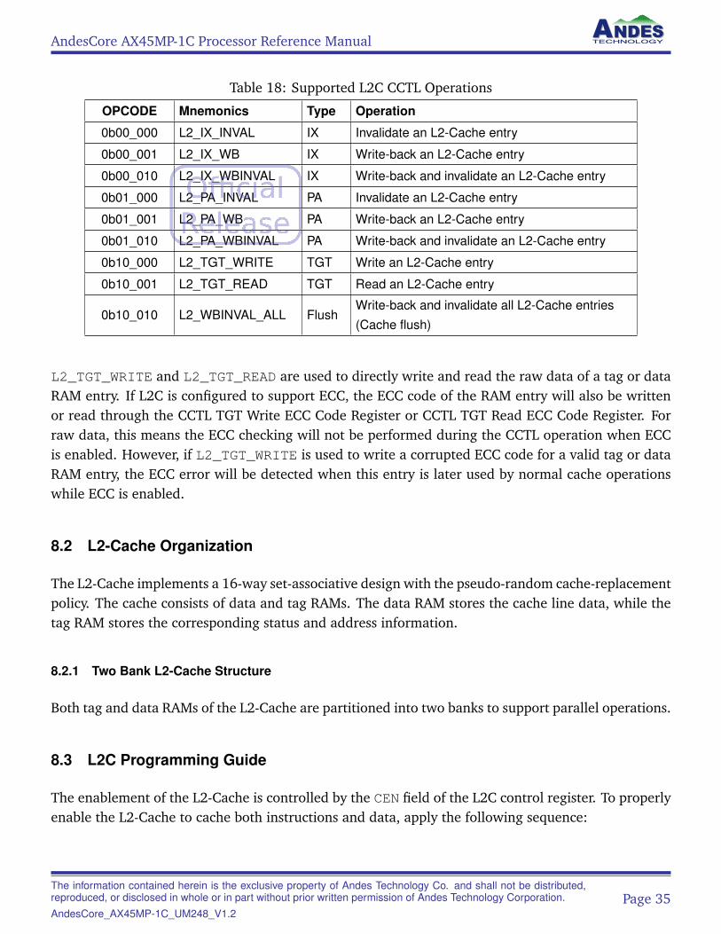
AndesCore AX45MP-1C Processor Reference Manual
Table 18: Supported L2C CCTL Operations
OPCODE Mnemonics Type Operation
0b00_000 L2_IX_INVAL IX Invalidate an L2-Cache entry
0b00_001 L2_IX_WB IX Write-back an L2-Cache entry
0b00_010 L2_IX_WBINVAL IX Write-back and invalidate an L2-Cache entry
0b01_000 L2_PA_INVAL PA Invalidate an L2-Cache entry
0b01_001 L2_PA_WB PA Write-back an L2-Cache entry
0b01_010 L2_PA_WBINVAL PA Write-back and invalidate an L2-Cache entry
0b10_000 L2_TGT_WRITE TGT Write an L2-Cache entry
0b10_001 L2_TGT_READ TGT Read an L2-Cache entry
0b10_010 L2_WBINVAL_ALL FlushWrite-back and invalidate all L2-Cache entries(Cache flush)
L2_TGT_WRITE and L2_TGT_READ are used to directly write and read the raw data of a tag or dataRAM entry. If L2C is configured to support ECC, the ECC code of the RAM entry will also be writtenor read through the CCTL TGT Write ECC Code Register or CCTL TGT Read ECC Code Register. Forraw data, this means the ECC checking will not be performed during the CCTL operation when ECCis enabled. However, if L2_TGT_WRITE is used to write a corrupted ECC code for a valid tag or dataRAM entry, the ECC error will be detected when this entry is later used by normal cache operationswhile ECC is enabled.
8.2 L2-Cache Organization
The L2-Cache implements a 16-way set-associative design with the pseudo-random cache-replacementpolicy. The cache consists of data and tag RAMs. The data RAM stores the cache line data, while thetag RAM stores the corresponding status and address information.
8.2.1 Two Bank L2-Cache Structure
Both tag and data RAMs of the L2-Cache are partitioned into two banks to support parallel operations.
8.3 L2C Programming Guide
The enablement of the L2-Cache is controlled by the CEN field of the L2C control register. To properlyenable the L2-Cache to cache both instructions and data, apply the following sequence:
The information contained herein is the exclusive property of Andes Technology Co. and shall not be distributed,reproduced, or disclosed in whole or in part without prior written permission of Andes Technology Corporation.AndesCore_AX45MP-1C_UM248_V1.2
Page 35
AndesCore AX45MP-1C Processor Reference Manual
1. Configure related L2C functions by writing the L2C control register with desired values for thePFTHRES, IPFDPT, DPFDPT, ECCEN, TRAMOCTL, TRAMICTL, DRAMOCTL and DRAMICTL fields.The CEN field should be set to 0. This step can be skipped if the resulting write value is 0.
2. Write the L2C control register again using the same value of step 1 with the CEN field being 1.
To disable the L2-Cache to stop caching both instructions and data, apply the following sequence:
1. Write 0 to the CEN field of the L2C control register.2. Write-back and invalidate the L2-Cache by using the CCTL flush command (L2_WBINVAL_ALL)
as described in Section 8.4.11.
8.4 L2-Cache Controller Registers
L2C controller registers are memory mapped to a 1MiB space for access through normal RISC-V load-/store instructions. The base address of this 1MiB space is decided by the L2C Register Base option.The cacheability of bus transactions to this region is ignored and only SINGLE transactions are sup-ported. The result of using other burst types of transactions to access this region is UNPREDICTABLE.
8.4.1 Register Type
Term Description
IM Implementation dependent/determined
RO Read-Only register/field. Any software write to RO registers/fields will be silently ignored byhardware.
RW Read/Write register/field
W1C Write-One-Clear register/field. When written 1, the corresponding bit of the register/field iscleared to 0.
WC Write-Clear register/field. When written any value, the register/field is cleared to 0.
8.4.2 Summary of Registers
The summary of registers is shown in Table 19.
Table 19: L2C Register Summary
Address Offset Description Section
0x0000 – 0x0007 Configuration Register Section 8.4.3
0x0008 – 0x000f Control Register Section 8.4.4
Continued on next page. . .
The information contained herein is the exclusive property of Andes Technology Co. and shall not be distributed,reproduced, or disclosed in whole or in part without prior written permission of Andes Technology Corporation.AndesCore_AX45MP-1C_UM248_V1.2
Page 36
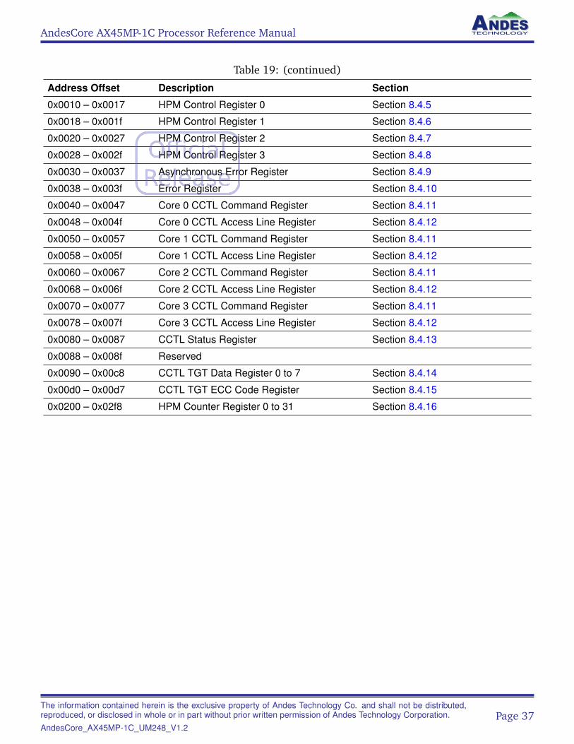
AndesCore AX45MP-1C Processor Reference Manual
Table 19: (continued)
Address Offset Description Section
0x0010 – 0x0017 HPM Control Register 0 Section 8.4.5
0x0018 – 0x001f HPM Control Register 1 Section 8.4.6
0x0020 – 0x0027 HPM Control Register 2 Section 8.4.7
0x0028 – 0x002f HPM Control Register 3 Section 8.4.8
0x0030 – 0x0037 Asynchronous Error Register Section 8.4.9
0x0038 – 0x003f Error Register Section 8.4.10
0x0040 – 0x0047 Core 0 CCTL Command Register Section 8.4.11
0x0048 – 0x004f Core 0 CCTL Access Line Register Section 8.4.12
0x0050 – 0x0057 Core 1 CCTL Command Register Section 8.4.11
0x0058 – 0x005f Core 1 CCTL Access Line Register Section 8.4.12
0x0060 – 0x0067 Core 2 CCTL Command Register Section 8.4.11
0x0068 – 0x006f Core 2 CCTL Access Line Register Section 8.4.12
0x0070 – 0x0077 Core 3 CCTL Command Register Section 8.4.11
0x0078 – 0x007f Core 3 CCTL Access Line Register Section 8.4.12
0x0080 – 0x0087 CCTL Status Register Section 8.4.13
0x0088 – 0x008f Reserved
0x0090 – 0x00c8 CCTL TGT Data Register 0 to 7 Section 8.4.14
0x00d0 – 0x00d7 CCTL TGT ECC Code Register Section 8.4.15
0x0200 – 0x02f8 HPM Counter Register 0 to 31 Section 8.4.16
The information contained herein is the exclusive property of Andes Technology Co. and shall not be distributed,reproduced, or disclosed in whole or in part without prior written permission of Andes Technology Corporation.AndesCore_AX45MP-1C_UM248_V1.2
Page 37
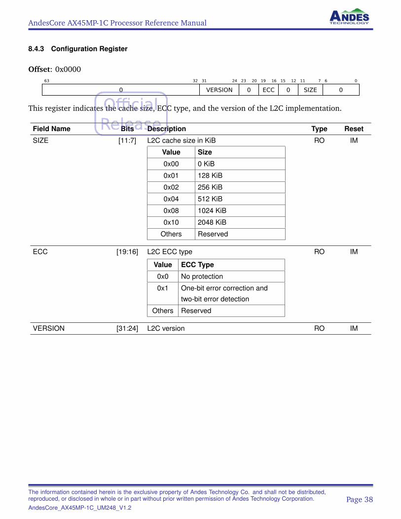
AndesCore AX45MP-1C Processor Reference Manual
8.4.3 Configuration Register
Offset: 0x000063 32
0
31 24
VERSION
23 20
0
19 16
ECC
15 12
0
11 7
SIZE
6 0
0
This register indicates the cache size, ECC type, and the version of the L2C implementation.
Field Name Bits Description Type Reset
SIZE [11:7] L2C cache size in KiB
Value Size
0x00 0 KiB
0x01 128 KiB
0x02 256 KiB
0x04 512 KiB
0x08 1024 KiB
0x10 2048 KiB
Others Reserved
RO IM
ECC [19:16] L2C ECC type
Value ECC Type
0x0 No protection
0x1 One-bit error correction andtwo-bit error detection
Others Reserved
RO IM
VERSION [31:24] L2C version RO IM
The information contained herein is the exclusive property of Andes Technology Co. and shall not be distributed,reproduced, or disclosed in whole or in part without prior written permission of Andes Technology Corporation.AndesCore_AX45MP-1C_UM248_V1.2
Page 38
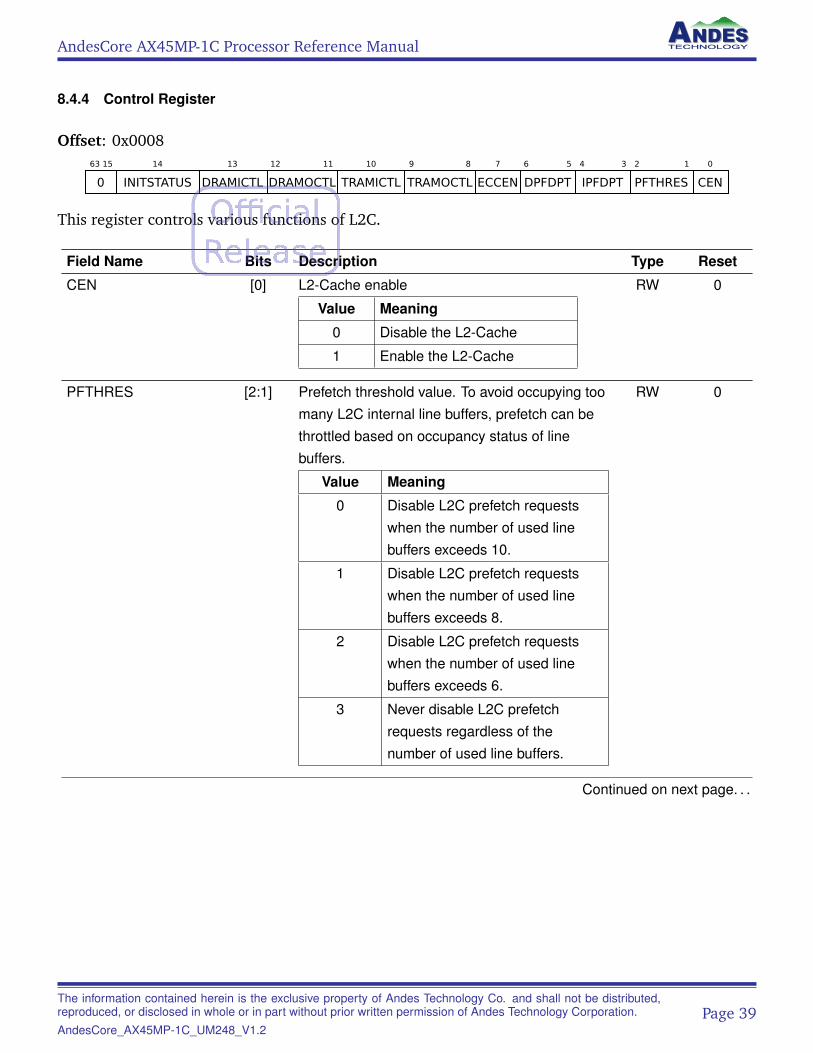
AndesCore AX45MP-1C Processor Reference Manual
8.4.4 Control Register
Offset: 0x000863 15
0
14
INITSTATUS
13
DRAMICTL
12 11
DRAMOCTL
10
TRAMICTL
9 8
TRAMOCTL
7
ECCEN
6 5
DPFDPT
4 3
IPFDPT
2 1
PFTHRES
0
CEN
This register controls various functions of L2C.
Field Name Bits Description Type Reset
CEN [0] L2-Cache enable
Value Meaning
0 Disable the L2-Cache
1 Enable the L2-Cache
RW 0
PFTHRES [2:1] Prefetch threshold value. To avoid occupying toomany L2C internal line buffers, prefetch can bethrottled based on occupancy status of linebuffers.
Value Meaning
0 Disable L2C prefetch requestswhen the number of used linebuffers exceeds 10.
1 Disable L2C prefetch requestswhen the number of used linebuffers exceeds 8.
2 Disable L2C prefetch requestswhen the number of used linebuffers exceeds 6.
3 Never disable L2C prefetchrequests regardless of thenumber of used line buffers.
RW 0
Continued on next page. . .
The information contained herein is the exclusive property of Andes Technology Co. and shall not be distributed,reproduced, or disclosed in whole or in part without prior written permission of Andes Technology Corporation.AndesCore_AX45MP-1C_UM248_V1.2
Page 39
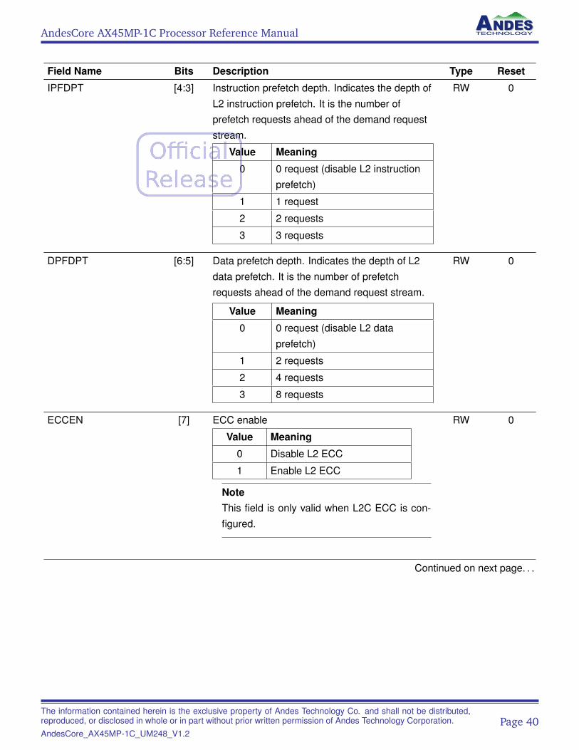
AndesCore AX45MP-1C Processor Reference Manual
Field Name Bits Description Type Reset
IPFDPT [4:3] Instruction prefetch depth. Indicates the depth ofL2 instruction prefetch. It is the number ofprefetch requests ahead of the demand requeststream.
Value Meaning
0 0 request (disable L2 instructionprefetch)
1 1 request
2 2 requests
3 3 requests
RW 0
DPFDPT [6:5] Data prefetch depth. Indicates the depth of L2data prefetch. It is the number of prefetchrequests ahead of the demand request stream.
Value Meaning
0 0 request (disable L2 dataprefetch)
1 2 requests
2 4 requests
3 8 requests
RW 0
ECCEN [7] ECC enable
Value Meaning
0 Disable L2 ECC
1 Enable L2 ECC
NoteThis field is only valid when L2C ECC is con-figured.
RW 0
Continued on next page. . .
The information contained herein is the exclusive property of Andes Technology Co. and shall not be distributed,reproduced, or disclosed in whole or in part without prior written permission of Andes Technology Corporation.AndesCore_AX45MP-1C_UM248_V1.2
Page 40
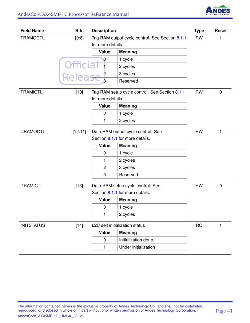
AndesCore AX45MP-1C Processor Reference Manual
Field Name Bits Description Type Reset
TRAMOCTL [9:8] Tag RAM output cycle control. See Section 8.1.1for more details.
Value Meaning
0 1 cycle
1 2 cycles
2 3 cycles
3 Reserved
RW 1
TRAMICTL [10] Tag RAM setup cycle control. See Section 8.1.1for more details.
Value Meaning
0 1 cycle
1 2 cycles
RW 0
DRAMOCTL [12:11] Data RAM output cycle control. SeeSection 8.1.1 for more details.
Value Meaning
0 1 cycle
1 2 cycles
2 3 cycles
3 Reserved
RW 1
DRAMICTL [13] Data RAM setup cycle control. SeeSection 8.1.1 for more details.
Value Meaning
0 1 cycle
1 2 cycles
RW 0
INITSTATUS [14] L2C self initialization status
Value Meaning
0 Initialization done
1 Under initialization
RO 1
The information contained herein is the exclusive property of Andes Technology Co. and shall not be distributed,reproduced, or disclosed in whole or in part without prior written permission of Andes Technology Corporation.AndesCore_AX45MP-1C_UM248_V1.2
Page 41
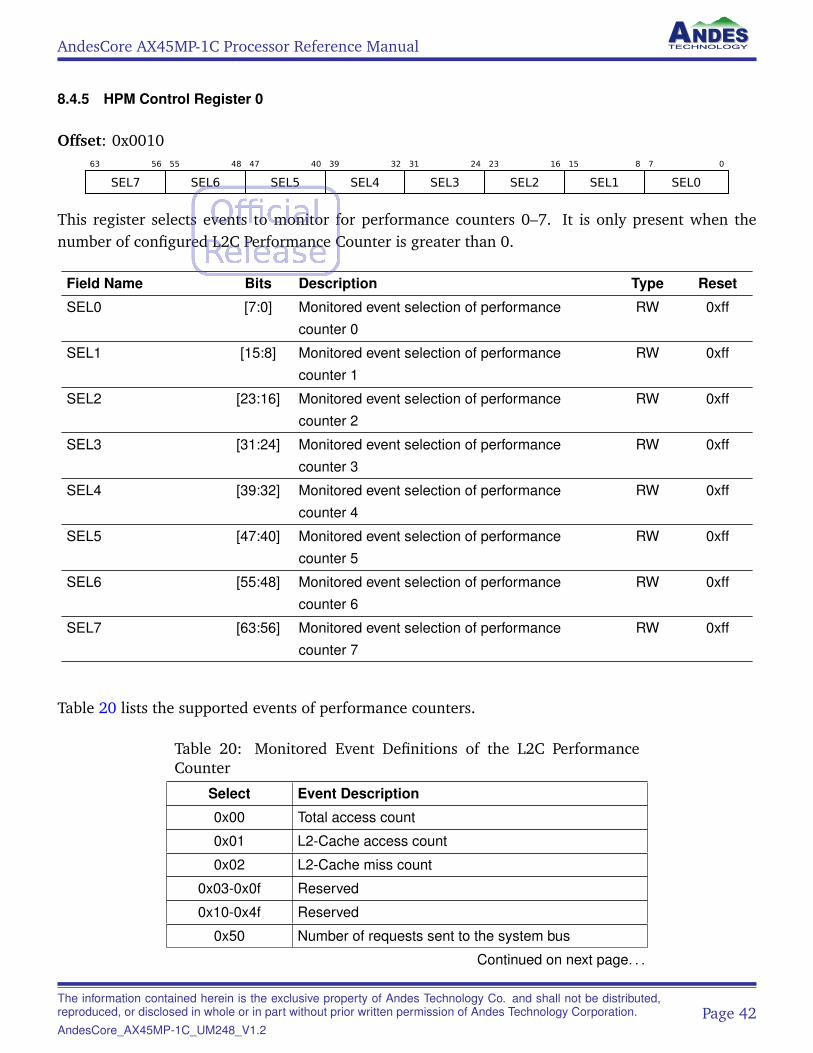
AndesCore AX45MP-1C Processor Reference Manual
8.4.5 HPM Control Register 0
Offset: 0x001063 56
SEL7
55 48
SEL6
47 40
SEL5
39 32
SEL4
31 24
SEL3
23 16
SEL2
15 8
SEL1
7 0
SEL0
This register selects events to monitor for performance counters 0–7. It is only present when thenumber of configured L2C Performance Counter is greater than 0.
Field Name Bits Description Type Reset
SEL0 [7:0] Monitored event selection of performancecounter 0
RW 0xff
SEL1 [15:8] Monitored event selection of performancecounter 1
RW 0xff
SEL2 [23:16] Monitored event selection of performancecounter 2
RW 0xff
SEL3 [31:24] Monitored event selection of performancecounter 3
RW 0xff
SEL4 [39:32] Monitored event selection of performancecounter 4
RW 0xff
SEL5 [47:40] Monitored event selection of performancecounter 5
RW 0xff
SEL6 [55:48] Monitored event selection of performancecounter 6
RW 0xff
SEL7 [63:56] Monitored event selection of performancecounter 7
RW 0xff
Table 20 lists the supported events of performance counters.
Table 20: Monitored Event Definitions of the L2C PerformanceCounter
Select Event Description
0x00 Total access count
0x01 L2-Cache access count
0x02 L2-Cache miss count
0x03-0x0f Reserved
0x10-0x4f Reserved
0x50 Number of requests sent to the system bus
Continued on next page. . .
The information contained herein is the exclusive property of Andes Technology Co. and shall not be distributed,reproduced, or disclosed in whole or in part without prior written permission of Andes Technology Corporation.AndesCore_AX45MP-1C_UM248_V1.2
Page 42
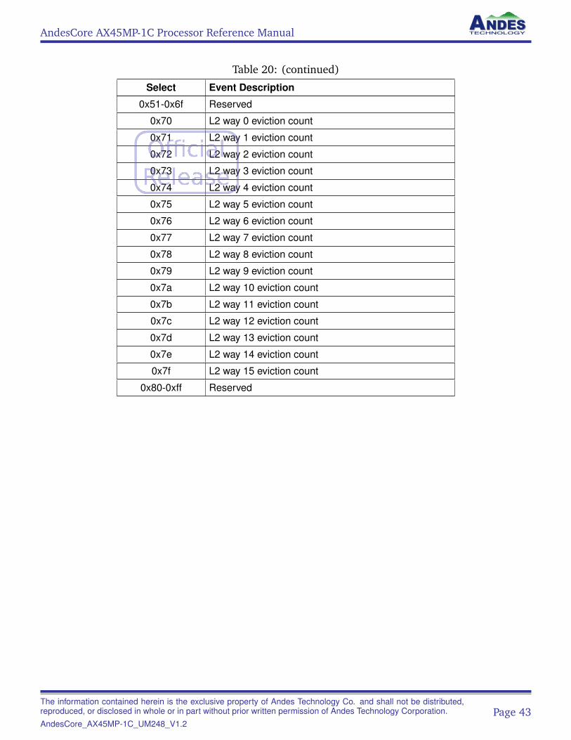
AndesCore AX45MP-1C Processor Reference Manual
Table 20: (continued)
Select Event Description
0x51-0x6f Reserved
0x70 L2 way 0 eviction count
0x71 L2 way 1 eviction count
0x72 L2 way 2 eviction count
0x73 L2 way 3 eviction count
0x74 L2 way 4 eviction count
0x75 L2 way 5 eviction count
0x76 L2 way 6 eviction count
0x77 L2 way 7 eviction count
0x78 L2 way 8 eviction count
0x79 L2 way 9 eviction count
0x7a L2 way 10 eviction count
0x7b L2 way 11 eviction count
0x7c L2 way 12 eviction count
0x7d L2 way 13 eviction count
0x7e L2 way 14 eviction count
0x7f L2 way 15 eviction count
0x80-0xff Reserved
The information contained herein is the exclusive property of Andes Technology Co. and shall not be distributed,reproduced, or disclosed in whole or in part without prior written permission of Andes Technology Corporation.AndesCore_AX45MP-1C_UM248_V1.2
Page 43

AndesCore AX45MP-1C Processor Reference Manual
8.4.6 HPM Control Register 1
Offset: 0x001863 56
SEL15
55 48
SEL14
47 40
SEL13
39 32
SEL12
31 24
SEL11
23 16
SEL10
15 8
SEL9
7 0
SEL8
This register selects the events to monitor for performance counters 8–15. It is only present when thenumber of configured L2C Performance Counter is greater than 8.
Field Name Bits Description Type Reset
SEL8 [7:0] Monitored event selection of performancecounter 8
RW 0xff
SEL9 [15:8] Monitored event selection of performancecounter 9
RW 0xff
SEL10 [23:16] Monitored event selection of performancecounter 10
RW 0xff
SEL11 [31:24] Monitored event selection of performancecounter 11
RW 0xff
SEL12 [39:32] Monitored event selection of performancecounter 12
RW 0xff
SEL13 [47:40] Monitored event selection of performancecounter 13
RW 0xff
SEL14 [55:48] Monitored event selection of performancecounter 14
RW 0xff
SEL15 [63:56] Monitored event selection of performancecounter 15
RW 0xff
The information contained herein is the exclusive property of Andes Technology Co. and shall not be distributed,reproduced, or disclosed in whole or in part without prior written permission of Andes Technology Corporation.AndesCore_AX45MP-1C_UM248_V1.2
Page 44

AndesCore AX45MP-1C Processor Reference Manual
8.4.7 HPM Control Register 2
Offset: 0x002063 56
SEL23
55 48
SEL22
47 40
SEL21
39 32
SEL20
31 24
SEL19
23 16
SEL18
15 8
SEL17
7 0
SEL16
This register selects the events to monitor for performance counters 16–23. It is only present whenthe number of configured L2C Performance Counter is greater than 16.
Field Name Bits Description Type Reset
SEL16 [7:0] Monitored event selection of performancecounter 16
RW 0xff
SEL17 [15:8] Monitored event selection of performancecounter 17
RW 0xff
SEL18 [23:16] Monitored event selection of performancecounter 18
RW 0xff
SEL19 [31:24] Monitored event selection of performancecounter 19
RW 0xff
SEL20 [39:32] Monitored event selection of performancecounter 20
RW 0xff
SEL21 [47:40] Monitored event selection of performancecounter 21
RW 0xff
SEL22 [55:48] Monitored event selection of performancecounter 22
RW 0xff
SEL23 [63:56] Monitored event selection of performancecounter 23
RW 0xff
The information contained herein is the exclusive property of Andes Technology Co. and shall not be distributed,reproduced, or disclosed in whole or in part without prior written permission of Andes Technology Corporation.AndesCore_AX45MP-1C_UM248_V1.2
Page 45
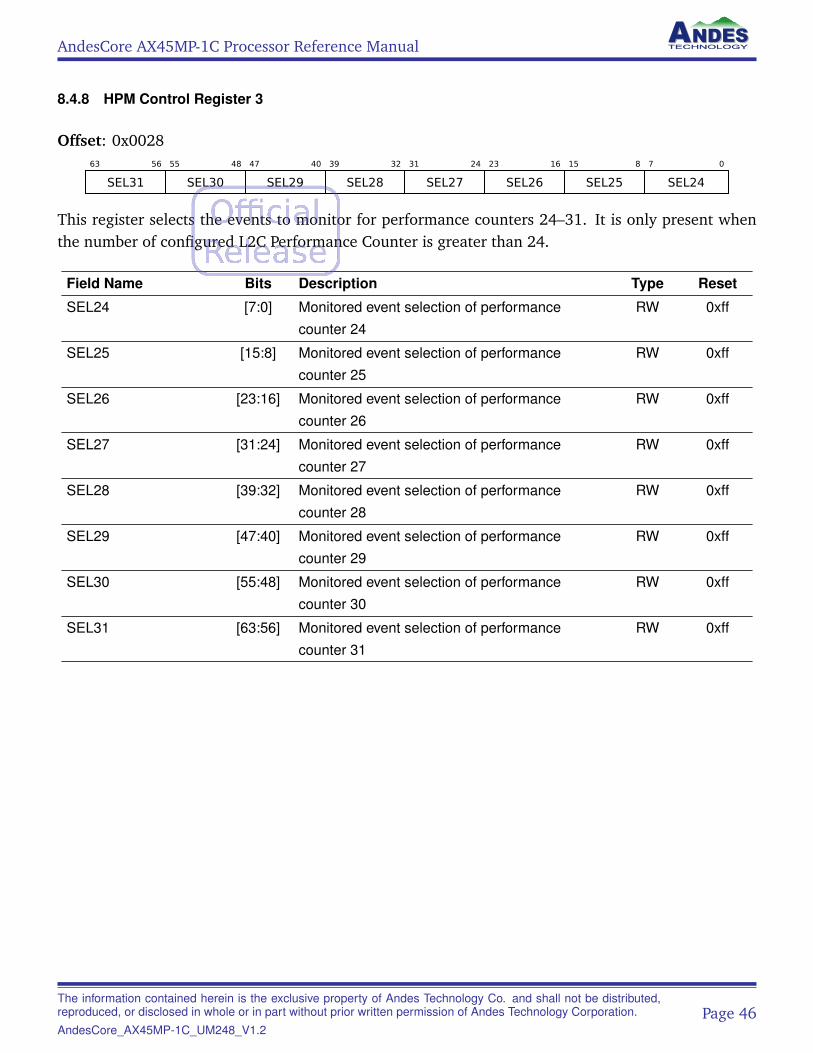
AndesCore AX45MP-1C Processor Reference Manual
8.4.8 HPM Control Register 3
Offset: 0x002863 56
SEL31
55 48
SEL30
47 40
SEL29
39 32
SEL28
31 24
SEL27
23 16
SEL26
15 8
SEL25
7 0
SEL24
This register selects the events to monitor for performance counters 24–31. It is only present whenthe number of configured L2C Performance Counter is greater than 24.
Field Name Bits Description Type Reset
SEL24 [7:0] Monitored event selection of performancecounter 24
RW 0xff
SEL25 [15:8] Monitored event selection of performancecounter 25
RW 0xff
SEL26 [23:16] Monitored event selection of performancecounter 26
RW 0xff
SEL27 [31:24] Monitored event selection of performancecounter 27
RW 0xff
SEL28 [39:32] Monitored event selection of performancecounter 28
RW 0xff
SEL29 [47:40] Monitored event selection of performancecounter 29
RW 0xff
SEL30 [55:48] Monitored event selection of performancecounter 30
RW 0xff
SEL31 [63:56] Monitored event selection of performancecounter 31
RW 0xff
The information contained herein is the exclusive property of Andes Technology Co. and shall not be distributed,reproduced, or disclosed in whole or in part without prior written permission of Andes Technology Corporation.AndesCore_AX45MP-1C_UM248_V1.2
Page 46
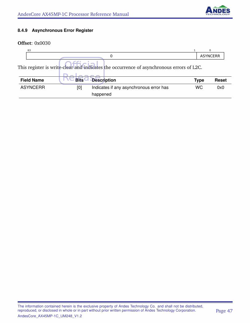
AndesCore AX45MP-1C Processor Reference Manual
8.4.9 Asynchronous Error Register
Offset: 0x003063 1
0
0
ASYNCERR
This register is write-clear and indicates the occurrence of asynchronous errors of L2C.
Field Name Bits Description Type Reset
ASYNCERR [0] Indicates if any asynchronous error hashappened
WC 0x0
The information contained herein is the exclusive property of Andes Technology Co. and shall not be distributed,reproduced, or disclosed in whole or in part without prior written permission of Andes Technology Corporation.AndesCore_AX45MP-1C_UM248_V1.2
Page 47
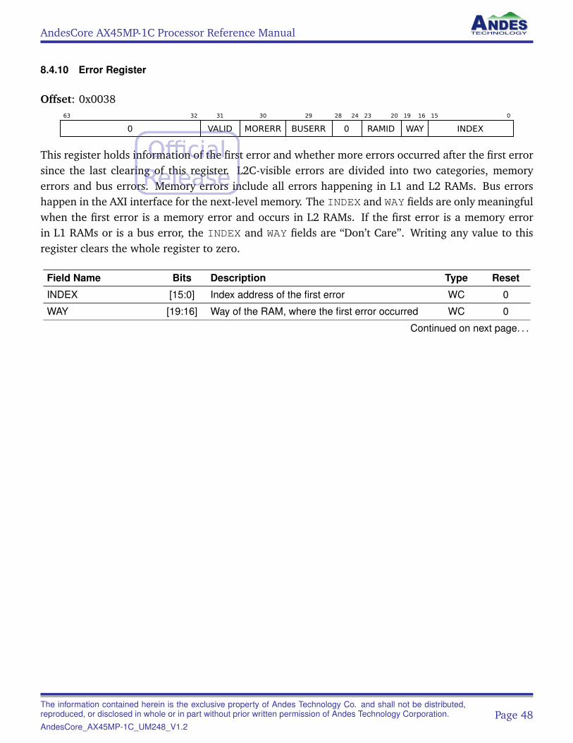
AndesCore AX45MP-1C Processor Reference Manual
8.4.10 Error Register
Offset: 0x003863 32
0
31
VALID
30
MORERR
29
BUSERR
28 24
0
23 20
RAMID
19 16
WAY
15 0
INDEX
This register holds information of the first error and whether more errors occurred after the first errorsince the last clearing of this register. L2C-visible errors are divided into two categories, memoryerrors and bus errors. Memory errors include all errors happening in L1 and L2 RAMs. Bus errorshappen in the AXI interface for the next-level memory. The INDEX and WAY fields are only meaningfulwhen the first error is a memory error and occurs in L2 RAMs. If the first error is a memory errorin L1 RAMs or is a bus error, the INDEX and WAY fields are “Don’t Care”. Writing any value to thisregister clears the whole register to zero.
Field Name Bits Description Type Reset
INDEX [15:0] Index address of the first error WC 0
WAY [19:16] Way of the RAM, where the first error occurred WC 0
Continued on next page. . .
The information contained herein is the exclusive property of Andes Technology Co. and shall not be distributed,reproduced, or disclosed in whole or in part without prior written permission of Andes Technology Corporation.AndesCore_AX45MP-1C_UM248_V1.2
Page 48
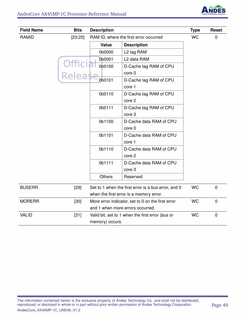
AndesCore AX45MP-1C Processor Reference Manual
Field Name Bits Description Type Reset
RAMID [23:20] RAM ID, where the first error occurred
Value Description
0b0000 L2 tag RAM
0b0001 L2 data RAM
0b0100 D-Cache tag RAM of CPUcore 0
0b0101 D-Cache tag RAM of CPUcore 1
0b0110 D-Cache tag RAM of CPUcore 2
0b0111 D-Cache tag RAM of CPUcore 3
0b1100 D-Cache data RAM of CPUcore 0
0b1101 D-Cache data RAM of CPUcore 1
0b1110 D-Cache data RAM of CPUcore 2
0b1111 D-Cache data RAM of CPUcore 3
Others Reserved
WC 0
BUSERR [29] Set to 1 when the first error is a bus error, and 0when the first error is a memory error.
WC 0
MORERR [30] More error indicator, set to 0 on the first errorand 1 when more errors occurred.
WC 0
VALID [31] Valid bit, set to 1 when the first error (bus ormemory) occurs.
WC 0
The information contained herein is the exclusive property of Andes Technology Co. and shall not be distributed,reproduced, or disclosed in whole or in part without prior written permission of Andes Technology Corporation.AndesCore_AX45MP-1C_UM248_V1.2
Page 49
AndesCore AX45MP-1C Processor Reference Manual
8.4.11 CCTL Command Registers 0 – 3
Offset: 0x0040, 0x0050, 0x0060, 0x007063 5
0
4 0
OPCODE
Writing to CCTL Command Register n (n=0 – 3) will trigger a CCTL operation, with the operationspecified by the value written and the line specified by CCTL Access Line Register n. Each registercorresponds to one CPU core so each CPU core should only use its respective registers. If CPU core ndoes not exist, CCTL Command Register n is reserved. L2C internally uses the round-robin strategyto decide the run order when two or more CCTL Command Registers are written at the same time.
Field Name Bits Description Type Reset
OPCODE [4:0] CCTL operation RW 0
The information contained herein is the exclusive property of Andes Technology Co. and shall not be distributed,reproduced, or disclosed in whole or in part without prior written permission of Andes Technology Corporation.AndesCore_AX45MP-1C_UM248_V1.2
Page 50
AndesCore AX45MP-1C Processor Reference Manual
8.4.12 CCTL Access Line Registers 0 – 3
Offset: 0x0048, 0x0058, 0x0068, 0x0078
These registers are used to specify the physical address, set, way, and/or RAM ID for CCTL operations.Each register corresponds to one CPU core so each CPU core should only use its respective register. IfCPU core n (n=0 – 3) does not exist, CCTL Access Line Register n is reserved.
The interpretation of these registers is different based on the CCTL operation type. The register formatfor IX-type CCTL operations is:
63 32
0
31 28
WAY
27 20
0
19 6
SET
5 0
0
Field Name Bits Description Type Reset
SET [19:6] Cache set of the CCTL operation RW 0
WAY [31:28] Cache way of the CCTL operation RW 0
The register format for PA-type CCTL operations is:
63 0
PA
Field Name Bits Description Type Reset
PA [63:0] Physical address of the CCTL operation RW 0
The register format for TGT-type CCTL operations is:
63 32
0
31 28
WAY
27 26
RAMID
25 20
0
19 6
SET
5 0
0
Field Name Bits Description Type Reset
SET [19:6] Cache set of the CCTL operation RW 0
RAMID [27:26] RAM ID of the CCTL operation
Value Meaning
0b00 L2 tag RAM
0b01 L2 data RAM
RW 0
WAY [31:28] Cache way of the CCTL operation RW 0
The information contained herein is the exclusive property of Andes Technology Co. and shall not be distributed,reproduced, or disclosed in whole or in part without prior written permission of Andes Technology Corporation.AndesCore_AX45MP-1C_UM248_V1.2
Page 51
AndesCore AX45MP-1C Processor Reference Manual
As for the flush type, these registers are not used.
The information contained herein is the exclusive property of Andes Technology Co. and shall not be distributed,reproduced, or disclosed in whole or in part without prior written permission of Andes Technology Corporation.AndesCore_AX45MP-1C_UM248_V1.2
Page 52
AndesCore AX45MP-1C Processor Reference Manual
8.4.13 CCTL Status Register
Offset: 0x008015 12
STATUS3
11 8
STATUS2
7 4
STATUS1
3 0
STATUS0
This register provides the status of CCTL operations.
Field Name Bits Description Type Reset
STATUS0 [3:0] CCTL status of Master (Core) 0
Value Meaning
0b0000 Idle
0b0001 A CCTL operation isrunning
0b0010 An illegal CCTL operationwas performed
Others Reserved
RO 0
STATUS1 [7:4] CCTL status of Master (Core) 1 RO 0
STATUS2 [11:8] CCTL status of Master (Core) 2 RO 0
STATUS3 [15:12] CCTL status of Master (Core) 3 RO 0
The information contained herein is the exclusive property of Andes Technology Co. and shall not be distributed,reproduced, or disclosed in whole or in part without prior written permission of Andes Technology Corporation.AndesCore_AX45MP-1C_UM248_V1.2
Page 53
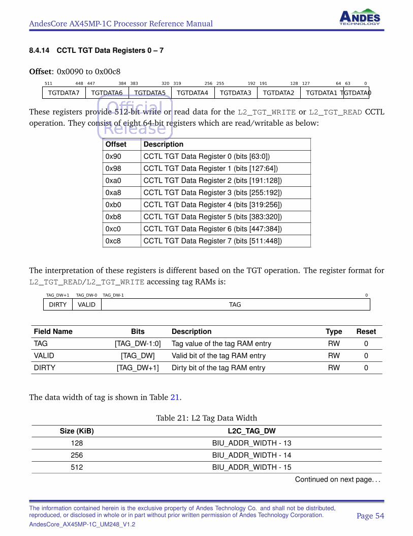
AndesCore AX45MP-1C Processor Reference Manual
8.4.14 CCTL TGT Data Registers 0 – 7
Offset: 0x0090 to 0x00c8511 448
TGTDATA7
447 384
TGTDATA6
383 320
TGTDATA5
319 256
TGTDATA4
255 192
TGTDATA3
191 128
TGTDATA2
127 64
TGTDATA1
63 0
TGTDATA0
These registers provide 512-bit write or read data for the L2_TGT_WRITE or L2_TGT_READ CCTLoperation. They consist of eight 64-bit registers which are read/writable as below:
Offset Description
0x90 CCTL TGT Data Register 0 (bits [63:0])
0x98 CCTL TGT Data Register 1 (bits [127:64])
0xa0 CCTL TGT Data Register 2 (bits [191:128])
0xa8 CCTL TGT Data Register 3 (bits [255:192])
0xb0 CCTL TGT Data Register 4 (bits [319:256])
0xb8 CCTL TGT Data Register 5 (bits [383:320])
0xc0 CCTL TGT Data Register 6 (bits [447:384])
0xc8 CCTL TGT Data Register 7 (bits [511:448])
The interpretation of these registers is different based on the TGT operation. The register format forL2_TGT_READ/L2_TGT_WRITE accessing tag RAMs is:
TAG_DW+1
DIRTY
TAG_DW-0
VALID
TAG_DW-1 0
TAG
Field Name Bits Description Type Reset
TAG [TAG_DW-1:0] Tag value of the tag RAM entry RW 0
VALID [TAG_DW] Valid bit of the tag RAM entry RW 0
DIRTY [TAG_DW+1] Dirty bit of the tag RAM entry RW 0
The data width of tag is shown in Table 21.
Table 21: L2 Tag Data Width
Size (KiB) L2C_TAG_DW
128 BIU_ADDR_WIDTH - 13
256 BIU_ADDR_WIDTH - 14
512 BIU_ADDR_WIDTH - 15
Continued on next page. . .
The information contained herein is the exclusive property of Andes Technology Co. and shall not be distributed,reproduced, or disclosed in whole or in part without prior written permission of Andes Technology Corporation.AndesCore_AX45MP-1C_UM248_V1.2
Page 54
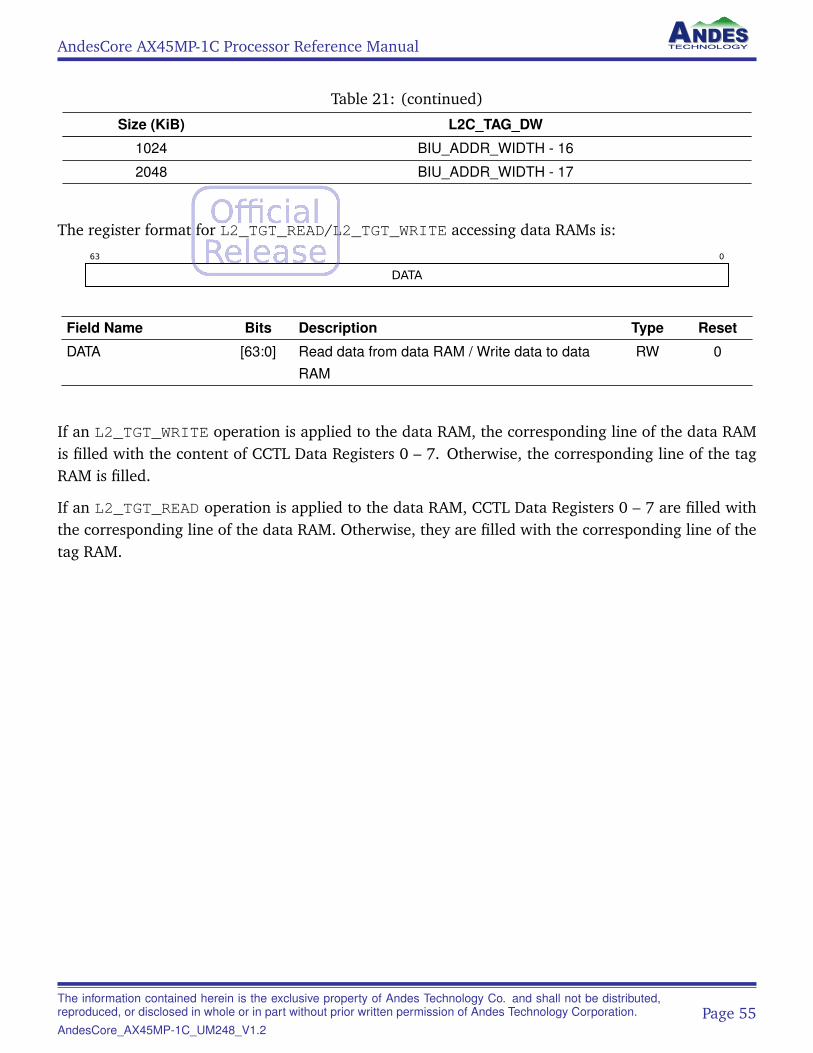
AndesCore AX45MP-1C Processor Reference Manual
Table 21: (continued)
Size (KiB) L2C_TAG_DW
1024 BIU_ADDR_WIDTH - 16
2048 BIU_ADDR_WIDTH - 17
The register format for L2_TGT_READ/L2_TGT_WRITE accessing data RAMs is:
63 0
DATA
Field Name Bits Description Type Reset
DATA [63:0] Read data from data RAM / Write data to dataRAM
RW 0
If an L2_TGT_WRITE operation is applied to the data RAM, the corresponding line of the data RAMis filled with the content of CCTL Data Registers 0 – 7. Otherwise, the corresponding line of the tagRAM is filled.
If an L2_TGT_READ operation is applied to the data RAM, CCTL Data Registers 0 – 7 are filled withthe corresponding line of the data RAM. Otherwise, they are filled with the corresponding line of thetag RAM.
The information contained herein is the exclusive property of Andes Technology Co. and shall not be distributed,reproduced, or disclosed in whole or in part without prior written permission of Andes Technology Corporation.AndesCore_AX45MP-1C_UM248_V1.2
Page 55
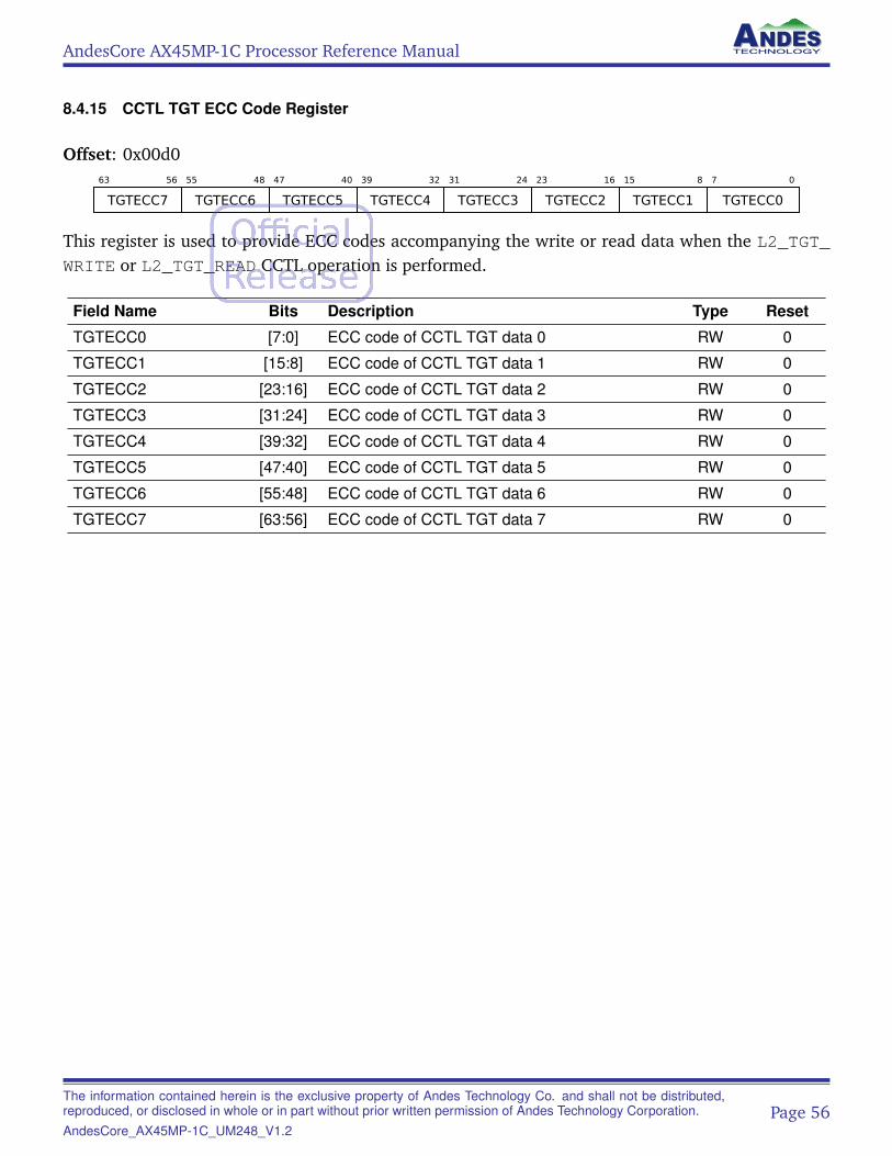
AndesCore AX45MP-1C Processor Reference Manual
8.4.15 CCTL TGT ECC Code Register
Offset: 0x00d063 56
TGTECC7
55 48
TGTECC6
47 40
TGTECC5
39 32
TGTECC4
31 24
TGTECC3
23 16
TGTECC2
15 8
TGTECC1
7 0
TGTECC0
This register is used to provide ECC codes accompanying the write or read data when the L2_TGT_WRITE or L2_TGT_READ CCTL operation is performed.
Field Name Bits Description Type Reset
TGTECC0 [7:0] ECC code of CCTL TGT data 0 RW 0
TGTECC1 [15:8] ECC code of CCTL TGT data 1 RW 0
TGTECC2 [23:16] ECC code of CCTL TGT data 2 RW 0
TGTECC3 [31:24] ECC code of CCTL TGT data 3 RW 0
TGTECC4 [39:32] ECC code of CCTL TGT data 4 RW 0
TGTECC5 [47:40] ECC code of CCTL TGT data 5 RW 0
TGTECC6 [55:48] ECC code of CCTL TGT data 6 RW 0
TGTECC7 [63:56] ECC code of CCTL TGT data 7 RW 0
The information contained herein is the exclusive property of Andes Technology Co. and shall not be distributed,reproduced, or disclosed in whole or in part without prior written permission of Andes Technology Corporation.AndesCore_AX45MP-1C_UM248_V1.2
Page 56
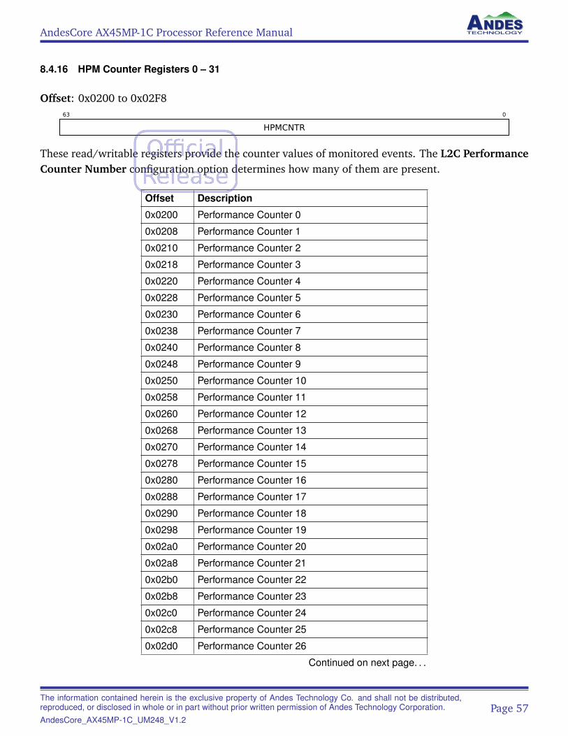
AndesCore AX45MP-1C Processor Reference Manual
8.4.16 HPM Counter Registers 0 – 31
Offset: 0x0200 to 0x02F863 0
HPMCNTR
These read/writable registers provide the counter values of monitored events. The L2C PerformanceCounter Number configuration option determines how many of them are present.
Offset Description
0x0200 Performance Counter 0
0x0208 Performance Counter 1
0x0210 Performance Counter 2
0x0218 Performance Counter 3
0x0220 Performance Counter 4
0x0228 Performance Counter 5
0x0230 Performance Counter 6
0x0238 Performance Counter 7
0x0240 Performance Counter 8
0x0248 Performance Counter 9
0x0250 Performance Counter 10
0x0258 Performance Counter 11
0x0260 Performance Counter 12
0x0268 Performance Counter 13
0x0270 Performance Counter 14
0x0278 Performance Counter 15
0x0280 Performance Counter 16
0x0288 Performance Counter 17
0x0290 Performance Counter 18
0x0298 Performance Counter 19
0x02a0 Performance Counter 20
0x02a8 Performance Counter 21
0x02b0 Performance Counter 22
0x02b8 Performance Counter 23
0x02c0 Performance Counter 24
0x02c8 Performance Counter 25
0x02d0 Performance Counter 26
Continued on next page. . .
The information contained herein is the exclusive property of Andes Technology Co. and shall not be distributed,reproduced, or disclosed in whole or in part without prior written permission of Andes Technology Corporation.AndesCore_AX45MP-1C_UM248_V1.2
Page 57
AndesCore AX45MP-1C Processor Reference Manual
Offset Description
0x02d8 Performance Counter 27
0x02e0 Performance Counter 28
0x02e8 Performance Counter 29
0x02f0 Performance Counter 30
0x02f8 Performance Counter 31
The information contained herein is the exclusive property of Andes Technology Co. and shall not be distributed,reproduced, or disclosed in whole or in part without prior written permission of Andes Technology Corporation.AndesCore_AX45MP-1C_UM248_V1.2
Page 58
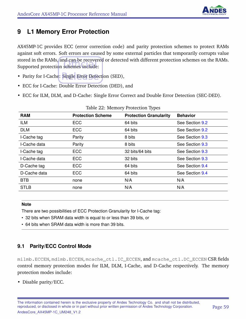
AndesCore AX45MP-1C Processor Reference Manual
9 L1 Memory Error Protection
AX45MP-1C provides ECC (error correction code) and parity protection schemes to protect RAMsagainst soft errors. Soft errors are caused by some external particles that temporarily corrupts valuestored in the RAMs, and can be recovered or detected with different protection schemes on the RAMs.Supported protection schemes include:
• Parity for I-Cache: Single Error Detection (SED),
• ECC for I-Cache: Double Error Detection (DED), and
• ECC for ILM, DLM, and D-Cache: Single Error Correct and Double Error Detection (SEC-DED).
Table 22: Memory Protection Types
RAM Protection Scheme Protection Granularity Behavior
ILM ECC 64 bits See Section 9.2
DLM ECC 64 bits See Section 9.2
I-Cache tag Parity 8 bits See Section 9.3
I-Cache data Parity 8 bits See Section 9.3
I-Cache tag ECC 32 bits/64 bits See Section 9.3
I-Cache data ECC 32 bits See Section 9.3
D-Cache tag ECC 64 bits See Section 9.4
D-Cache data ECC 64 bits See Section 9.4
BTB none N/A N/A
STLB none N/A N/A
NoteThere are two possibilities of ECC Protection Granularity for I-Cache tag:• 32 bits when SRAM data width is equal to or less than 39 bits, or• 64 bits when SRAM data width is more than 39 bits.
9.1 Parity/ECC Control Mode
milmb.ECCEN, mdlmb.ECCEN, mcache_ctl.IC_ECCEN, and mcache_ctl.DC_ECCEN CSR fieldscontrol memory protection modes for ILM, DLM, I-Cache, and D-Cache respectively. The memoryprotection modes include:
• Disable parity/ECC.
The information contained herein is the exclusive property of Andes Technology Co. and shall not be distributed,reproduced, or disclosed in whole or in part without prior written permission of Andes Technology Corporation.AndesCore_AX45MP-1C_UM248_V1.2
Page 59
AndesCore AX45MP-1C Processor Reference Manual
• Generate exceptions on uncorrectable parity/ECC errors.
• Generate exceptions on all parity/ECC errors.
See the following subsections for detailed information on each mode.
9.1.1 Disable Parity/ECC
The behavior of the parity/ECC logic in the “Disable parity/ECC” mode is:
• The logic disables parity/ECC checking, but still updates the newly-generated parity/ECC code intothe RAM for each write access.
• The received data is always uncorrected.
• The processor uses read-modify-writes to store a partial double word.
• If any parity/ECC error happens,
– No exception will be generated.
– The error will not be corrected.
9.1.2 Generate Exceptions on Uncorrectable Parity/ECC Errors
The behavior of the parity/ECC logic in the “Generate exceptions on uncorrectable parity/ECC errors”mode is:
• The logic enables parity/ECC checking and updates the newly-generated parity/ECC code into theRAM for each write access.
• Corrected data is always given.
• The processor uses read-modify-writes to store a partial double word.
• No exceptions will be generated if correctable errors are detected, and those correctable errors willbe recovered.
• An exception will still be generated if an uncorrectable error is detected.
• For speculative accesses, e.g. instruction prefetch and data prefetch,
– Uncorrectable errors does not generate exceptions
– Correctable errors are corrected
The information contained herein is the exclusive property of Andes Technology Co. and shall not be distributed,reproduced, or disclosed in whole or in part without prior written permission of Andes Technology Corporation.AndesCore_AX45MP-1C_UM248_V1.2
Page 60
AndesCore AX45MP-1C Processor Reference Manual
9.1.3 Generate Exceptions on Parity/ECC Errors
The behavior of the parity/ECC logic in the “Generate exceptions on parity/ECC errors” mode is:
• The logic enables parity/ECC checking and updates the newly-generated parity/ECC code into theRAM for each write access.
• Corrected data is always given.
• The processor uses read-modify-writes to store a partial double word.
• For correctable Parity/ECC errors, exceptions are generated, and the corrupted data in the RAMwill be corrected before generating exceptions.
• For uncorrectable Parity/ECC errors, exceptions are generated.
• For speculative accesses, e.g. instruction prefetch and data prefetch,
– Uncorrectable and correctable errors does not generate exceptions
– Correctable errors are corrected
9.2 Local Memory Protection
SECDED is applied to ILM and DLM when ILM or DLM Soft Error Protection is specified to ECC. One-bit ECC errors found on ILM/DLM access are correctable errors, while two-bit ECC errors found onload or store instructions on ILM/DLM are uncorrectable errors. For ILM/DLM ECC error exceptions,mecc_code will be updated with the ECC error information.
9.3 I-Cache Protection
SED and DED are applied to I-Cache when I-Cache Soft Error Protection is specified to Parity andECC respectively. Data in I-Cache are always clean since there are no store accesses to I-Cache. If aparity or ECC error is found, I-Cache can get the correct copy from the next-level memory system.Therefore, if one-bit parity errors or one-bit/two-bit ECC errors are found on I-Cache accesses, theywill be correctable errors. In order to check the soft-error on lock bit, another lock mirror bit isimplemented. If a parity error occurs on locked cache line, or the lock bit and the lock mirror bitare mismatched, that parity error will be an uncorrectable error. For I-Cache parity error exceptions,mecc_code will be updated with the parity/ECC error information. For lock bit information, use theCCTL instruction, L1I_IX_RTAG, to get the lock bit value.
The information contained herein is the exclusive property of Andes Technology Co. and shall not be distributed,reproduced, or disclosed in whole or in part without prior written permission of Andes Technology Corporation.AndesCore_AX45MP-1C_UM248_V1.2
Page 61
AndesCore AX45MP-1C Processor Reference Manual
9.4 D-Cache Protection
SEC-DED is applied to D-Cache tag and data SRAMs when D-Cache Soft Error Protection is specifiedto ECC. An access to a cache line with a one-bit error on tag or data SRAMs is correctable, and thehardware will automatically repair the error. An access to a clean line with a two-bit error on dataSRAMs is also correctable. The hardware will invalidate the line, and then fill the next-level memorysystem.
An access to a cache line with a two-bit error on tag SRAMs is uncorrectable. An access to a modifiedline with a two-bit error on data SRAMs is also uncorrectable. For D-Cache ECC error exceptions,mecc_code will be updated with the ECC error information.
9.5 Soft Error Injection
9.5.1 ILM/DLM ECC Error Injection
Use the following steps to inject ECC errors on ILM/DLM for implementing the ECC exception handler.
• Specify ILM/DLM to “Disable ECC” mode.
• Turn on milmb.RWECC or mdlmb.RWECC for ILM/DLM respectively.
• Perform a load instruction on an address in ILM/DLM region. Then, mecc_code.CODEwill containthe ECC code of the read data.
• Flip one or two bits in mecc_code.CODE to inject one-bit or two-bit ECC errors.
• Perform a store instruction to the address in ILM/DLM region. Then, the ECC code with error willbe written to ILM/DLM.
• Turn off milmb.RWECC or mdlmb.RWECC for ILM/DLM respectively.
• Specify ILM/DLM to “Generate Exceptions on Uncorrectable Parity/ECC Errors” mode or “GenerateExceptions on parity/ECC Errors” mode.
• Perform a load instruction to the address to trigger the ECC error.
9.5.2 I-Cache Parity/ECC Error Injection
Use the following steps to inject ECC errors on I-Cache for implementing the parity exception handler.
• Specify I-Cache to “Disable ECC” mode.
• Turn on mcache_ctl.IC_RWECC.
The information contained herein is the exclusive property of Andes Technology Co. and shall not be distributed,reproduced, or disclosed in whole or in part without prior written permission of Andes Technology Corporation.AndesCore_AX45MP-1C_UM248_V1.2
Page 62
AndesCore AX45MP-1C Processor Reference Manual
• Perform L1I_IX_RTAG or L1I_IX_RDATA CCTL command to a specific address to read parity datafrom tag RAM or data RAM respectively.
• Flip one bit in mecc_code.CODE or mcctldata to inject one bit parity error or flip the lockduplicate in mcctldata to generate a lock mismatch error.
• Perform L1I_IX_WTAG or L1I_IX_WDATA CCTL command to the specific address to inject a parityerror.
• Turn off mcache_ctl.IC_RWECC.
• Specify I-Cache to “Generate Exceptions on Uncorrectable Parity/ECC Errors” mode or “GenerateExceptions on parity/ECC Errors” mode.
• Perform a fetch to that specific address to trigger the ECC error.
9.5.3 D-Cache ECC Error Injection
Use the following steps to inject ECC errors on D-Cache for implementing the ECC exception handler.
• Specify D-Cache to “Disable ECC” mode.
• Turn on mcache_ctl.DC_RWECC.
• Perform L1D_IX_RTAG or L1D_IX_RDATA CCTL command to a specific address to read ECC datafrom tag RAM or data RAM respectively.
• Flip one bit or two bits in mecc_code.CODE and mcctldata to inject one-bit or two-bit ECCerrors.
• Perform L1D_IX_WTAG or L1D_IX_WDATA CCTL command to the specific address to inject an ECCerror.
• Turn off mcache_ctl.DC_RWECC.
• Specify D-Cache to “Generate Exceptions on Uncorrectable Parity/ECC Errors” mode or “GenerateExceptions on parity/ECC Errors” mode.
• Perform load/store fetch to that specific address to trigger the ECC error.
The information contained herein is the exclusive property of Andes Technology Co. and shall not be distributed,reproduced, or disclosed in whole or in part without prior written permission of Andes Technology Corporation.AndesCore_AX45MP-1C_UM248_V1.2
Page 63
AndesCore AX45MP-1C Processor Reference Manual
10 Physical Memory Attributes
10.1 Introduction
Memory locations can have various attributes associated with them, and are basically categorizedinto either one of the two types: device region and memory region. While memory regions may becacheable or non-cacheable locations, device regions are non-cacheable locations where accesses tothese locations may cause side effects. AX45MP-1C uses MTYP (memory type) to define the cacheabil-ity and idempotency of memory regions. Please see descriptions of the MTYP field in Section 16.17.1for possible values of MTYP.
AX45MP-1C provides two mechanisms for physical memory attributes:
• Static physical memory attributes
• Programmable physical memory attributes
10.2 Static Physical Memory Attributes
Up to 16 device regions could be statically configured in the processor through the Device Regionconfiguration options. The memory type attributes for device regions are (device, non-bufferable).
Device regions and ILM/DLM should not overlap with each other. The behavior is UNDEFINED whenthey overlap.
10.3 Programmable Physical Memory Attributes
Programmable PMA allows dynamic adjustment of memory attributes in the runtime. It contains aconfigurable amount of PMA entries implemented as CSR registers to control the attributes of memorylocations in interest. If the settings in those entries conflict with the static Device Region settings, PMAentries will have higher priorities.
PMA entries themselves are statically prioritized. The lowest-numbered PMA entry that matchesany physical address (PA) of the access determines the attribute type and whether to support AMOinstructions. If no PMA entries match the address, the attribute type is determined by the staticallyconfigured PMA. See Section 16.17.1 for more information about PMA entries.
The information contained herein is the exclusive property of Andes Technology Co. and shall not be distributed,reproduced, or disclosed in whole or in part without prior written permission of Andes Technology Corporation.AndesCore_AX45MP-1C_UM248_V1.2
Page 64
AndesCore AX45MP-1C Processor Reference Manual
10.4 Memory Access Ordering
Accesses to device regions are strongly-ordered. They are guaranteed to be non-speculative andissued in program order. An access to a device region is not issued until all preceding accesses todevice regions are finished.
On the other hand, accesses to the memory regions could be speculative and the order of accessingmemory regions is not guaranteed. A load access to a cacheable memory region might bypass anearlier store access if there is no data dependency. In such a scenario, explicit FENCE instructions arerequired to guarantee the order.
Table 23 shows ordering of two instructions A and B, where A < B (A comes earlier than B) in programorder.
Table 23: Memory Access Ordering
A<B in Program Order BA Cacheable
MemoryNon-
CacheableMemory
Device
Cacheable Memory - - -Non-Cacheable Memory - < <
Device - < <
10.5 Non-Cacheable Memory and Device Accesses
Accessing to non-cacheable memory and device will bypass I-Cache, D-Cache and L2-Cache no matterthe data is cached or not. The cache states are not changed by these accesses.
NoteFor CPU revisions before 10.0.0, instruction fetch will access I-Cache when data in non-cacheable memoryand device regions are cached into I-Cache. Under normal usages, data in non-cacheable memory anddevice regions are not cached unless PMA is changed from cacheable memory to non-cacheable memory ordevice regions.
10.6 Cacheable Memory Accesses to L1-Caches
This section describes operations to I-Cache and D-Cache.
The information contained herein is the exclusive property of Andes Technology Co. and shall not be distributed,reproduced, or disclosed in whole or in part without prior written permission of Andes Technology Corporation.AndesCore_AX45MP-1C_UM248_V1.2
Page 65
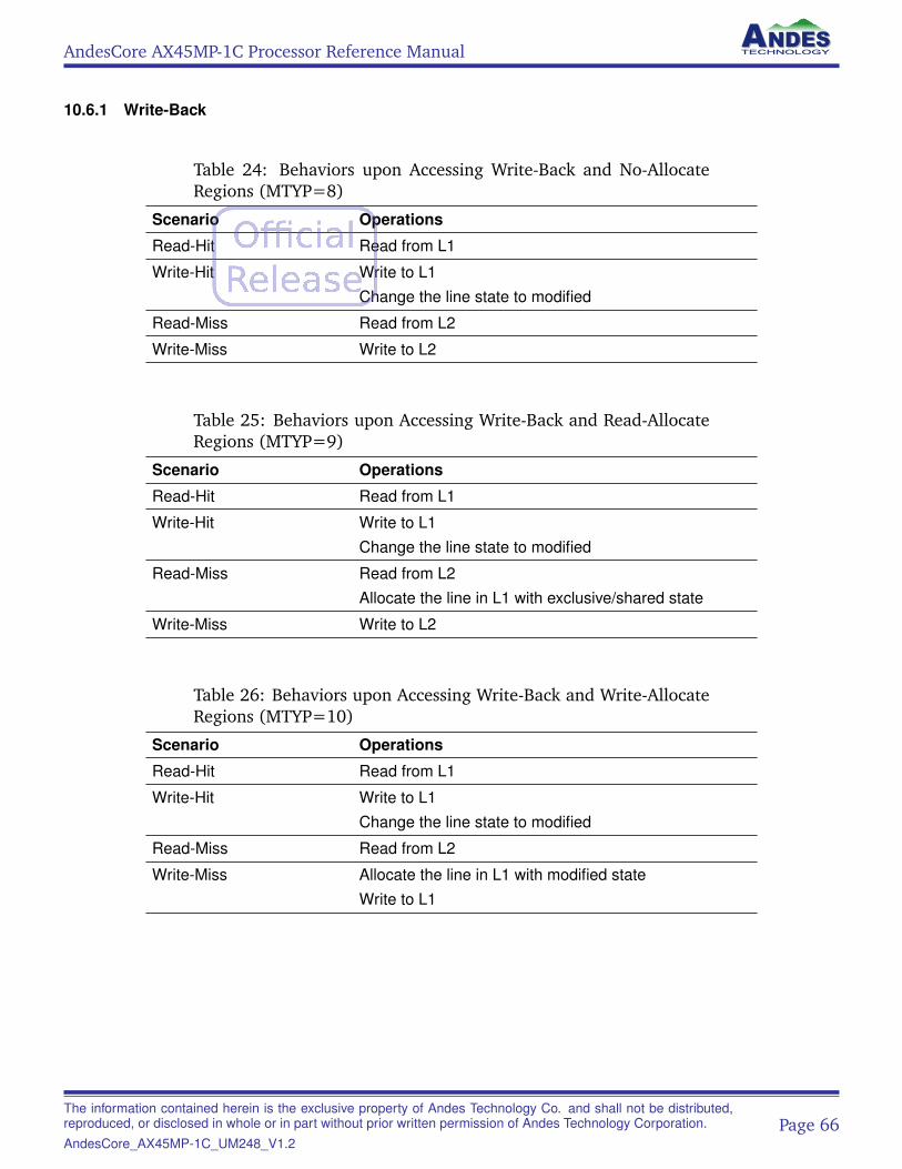
AndesCore AX45MP-1C Processor Reference Manual
10.6.1 Write-Back
Table 24: Behaviors upon Accessing Write-Back and No-AllocateRegions (MTYP=8)
Scenario Operations
Read-Hit Read from L1
Write-Hit Write to L1Change the line state to modified
Read-Miss Read from L2
Write-Miss Write to L2
Table 25: Behaviors upon Accessing Write-Back and Read-AllocateRegions (MTYP=9)
Scenario Operations
Read-Hit Read from L1
Write-Hit Write to L1Change the line state to modified
Read-Miss Read from L2Allocate the line in L1 with exclusive/shared state
Write-Miss Write to L2
Table 26: Behaviors upon Accessing Write-Back and Write-AllocateRegions (MTYP=10)
Scenario Operations
Read-Hit Read from L1
Write-Hit Write to L1Change the line state to modified
Read-Miss Read from L2
Write-Miss Allocate the line in L1 with modified stateWrite to L1
The information contained herein is the exclusive property of Andes Technology Co. and shall not be distributed,reproduced, or disclosed in whole or in part without prior written permission of Andes Technology Corporation.AndesCore_AX45MP-1C_UM248_V1.2
Page 66
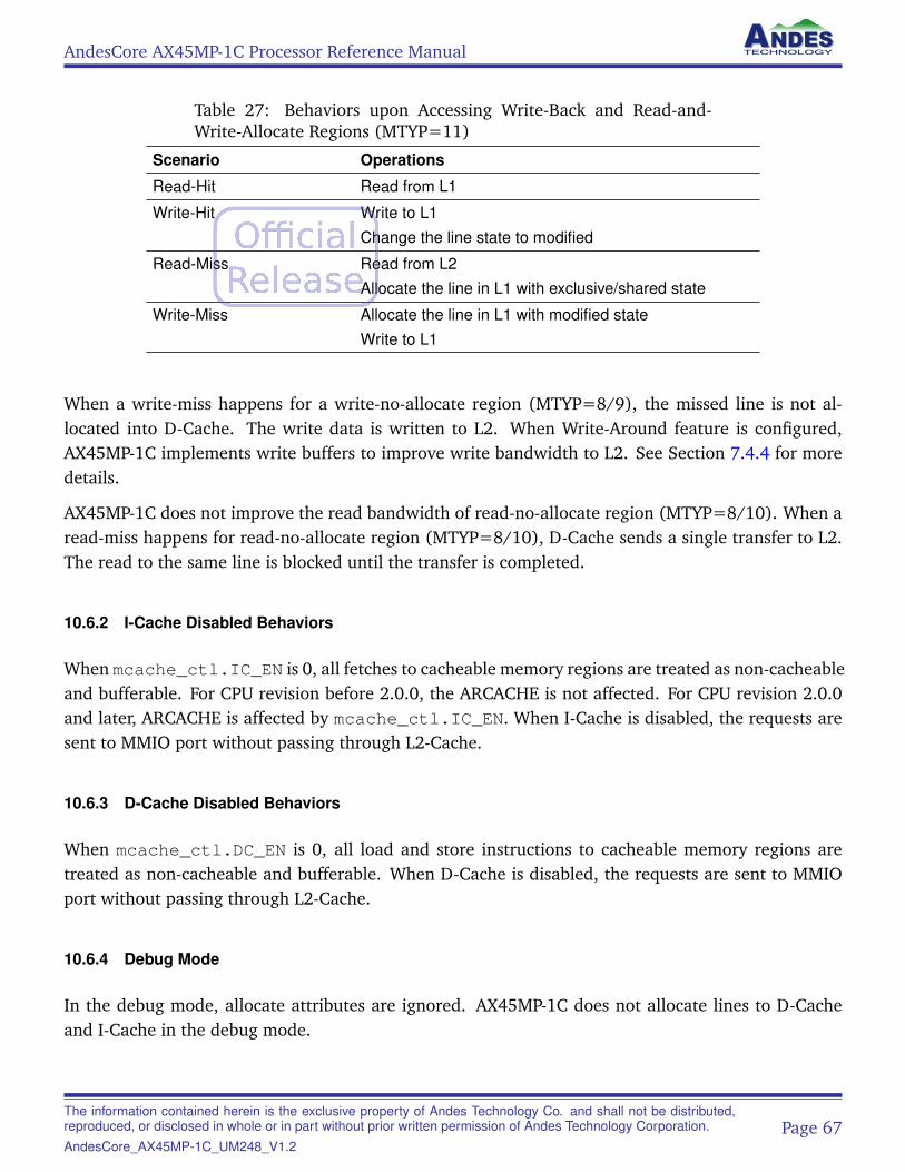
AndesCore AX45MP-1C Processor Reference Manual
Table 27: Behaviors upon Accessing Write-Back and Read-and-Write-Allocate Regions (MTYP=11)
Scenario Operations
Read-Hit Read from L1
Write-Hit Write to L1Change the line state to modified
Read-Miss Read from L2Allocate the line in L1 with exclusive/shared state
Write-Miss Allocate the line in L1 with modified stateWrite to L1
When a write-miss happens for a write-no-allocate region (MTYP=8/9), the missed line is not al-located into D-Cache. The write data is written to L2. When Write-Around feature is configured,AX45MP-1C implements write buffers to improve write bandwidth to L2. See Section 7.4.4 for moredetails.
AX45MP-1C does not improve the read bandwidth of read-no-allocate region (MTYP=8/10). When aread-miss happens for read-no-allocate region (MTYP=8/10), D-Cache sends a single transfer to L2.The read to the same line is blocked until the transfer is completed.
10.6.2 I-Cache Disabled Behaviors
When mcache_ctl.IC_EN is 0, all fetches to cacheable memory regions are treated as non-cacheableand bufferable. For CPU revision before 2.0.0, the ARCACHE is not affected. For CPU revision 2.0.0and later, ARCACHE is affected by mcache_ctl.IC_EN. When I-Cache is disabled, the requests aresent to MMIO port without passing through L2-Cache.
10.6.3 D-Cache Disabled Behaviors
When mcache_ctl.DC_EN is 0, all load and store instructions to cacheable memory regions aretreated as non-cacheable and bufferable. When D-Cache is disabled, the requests are sent to MMIOport without passing through L2-Cache.
10.6.4 Debug Mode
In the debug mode, allocate attributes are ignored. AX45MP-1C does not allocate lines to D-Cacheand I-Cache in the debug mode.
The information contained herein is the exclusive property of Andes Technology Co. and shall not be distributed,reproduced, or disclosed in whole or in part without prior written permission of Andes Technology Corporation.AndesCore_AX45MP-1C_UM248_V1.2
Page 67
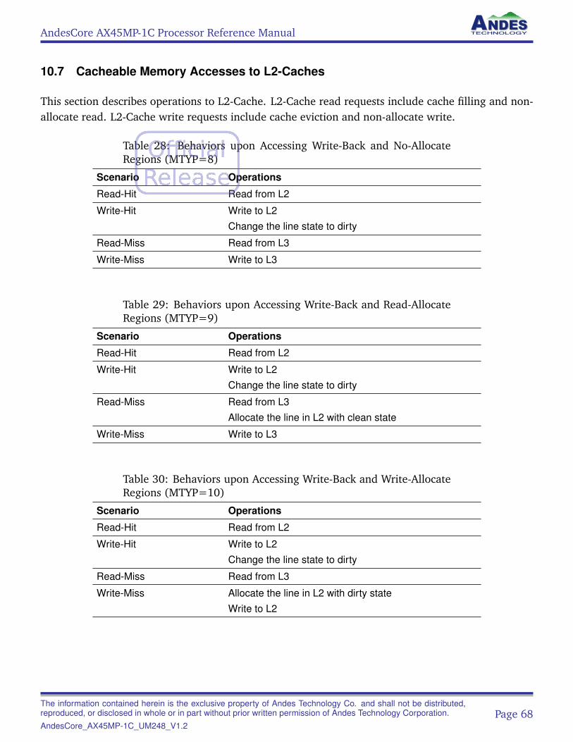
AndesCore AX45MP-1C Processor Reference Manual
10.7 Cacheable Memory Accesses to L2-Caches
This section describes operations to L2-Cache. L2-Cache read requests include cache filling and non-allocate read. L2-Cache write requests include cache eviction and non-allocate write.
Table 28: Behaviors upon Accessing Write-Back and No-AllocateRegions (MTYP=8)
Scenario Operations
Read-Hit Read from L2
Write-Hit Write to L2Change the line state to dirty
Read-Miss Read from L3
Write-Miss Write to L3
Table 29: Behaviors upon Accessing Write-Back and Read-AllocateRegions (MTYP=9)
Scenario Operations
Read-Hit Read from L2
Write-Hit Write to L2Change the line state to dirty
Read-Miss Read from L3Allocate the line in L2 with clean state
Write-Miss Write to L3
Table 30: Behaviors upon Accessing Write-Back and Write-AllocateRegions (MTYP=10)
Scenario Operations
Read-Hit Read from L2
Write-Hit Write to L2Change the line state to dirty
Read-Miss Read from L3
Write-Miss Allocate the line in L2 with dirty stateWrite to L2
The information contained herein is the exclusive property of Andes Technology Co. and shall not be distributed,reproduced, or disclosed in whole or in part without prior written permission of Andes Technology Corporation.AndesCore_AX45MP-1C_UM248_V1.2
Page 68
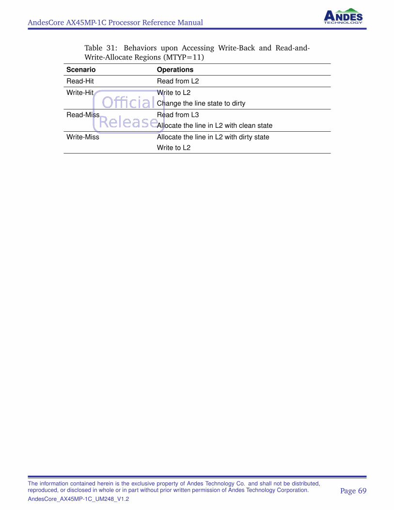
AndesCore AX45MP-1C Processor Reference Manual
Table 31: Behaviors upon Accessing Write-Back and Read-and-Write-Allocate Regions (MTYP=11)
Scenario Operations
Read-Hit Read from L2
Write-Hit Write to L2Change the line state to dirty
Read-Miss Read from L3Allocate the line in L2 with clean state
Write-Miss Allocate the line in L2 with dirty stateWrite to L2
The information contained herein is the exclusive property of Andes Technology Co. and shall not be distributed,reproduced, or disclosed in whole or in part without prior written permission of Andes Technology Corporation.AndesCore_AX45MP-1C_UM248_V1.2
Page 69
AndesCore AX45MP-1C Processor Reference Manual
11 MemBoost
11.1 Non-Blocking Memory Access
Non-blocking memory access hides memory latency by concurrently executing instructions and mem-ory accesses. Store instructions in AX45MP-1C are always non-blocking. Load instructions in AX45MP-1C are blocking by default, meaning that they will block all subsequent instructions until the requiredbus accesses are finished (e.g., on cache misses, or when D-Cache is disabled or non-present).
The control bit mmisc_ctl.NBLD_EN controls the blocking behavior of load instructions. Once set, loadinstructions to cacheable memory will be non-blocking, waiting in the background for bus accessesto finish, and allow subsequent instructions to continue execution until data dependency hazards orstructural hazards occur.
Data dependency hazards are hazards where subsequent instructions accessing the destination reg-isters of the load instructions. Structural hazards are the resource limitations to allow load/storeinstructions to wait in the background. The number of cacheable accesses is limited by the maximumoutstanding D-Cache misses.
When the processor operates in the non-blocking mode, the bus read transactions for the outstandingload/stores are each assigned a different AxID to allow the data to return out-of-order.
When load instructions operate in the blocking mode, bus aborts/errors are reported synchronouslyas Load Access Faults (mcause = 5). On the other hand, bus aborts/errors on load instructions willno longer be reported synchronously in the non-blocking mode. They will be treated as impreciseexceptions and reported as Bus Read/Write Transaction Error Local Interrupts (mip.BWEI).
Regardless of mmisc_ctl.NBLD_EN, the following memory access instructions are always blocking:
• Load instructions to device and non-cacheable memory
• Load instructions to local memory
• Load-Reserved/Store-Conditional instructions
• Atomic memory access (AMO) instructions
The information contained herein is the exclusive property of Andes Technology Co. and shall not be distributed,reproduced, or disclosed in whole or in part without prior written permission of Andes Technology Corporation.AndesCore_AX45MP-1C_UM248_V1.2
Page 70
AndesCore AX45MP-1C Processor Reference Manual
11.2 D-Cache Write-Around Support
Store operations to write-allocate memory will allocate a D-Cache entry on cache misses, in the hopethat the entry will later be used again. However, in some streaming cases, such as memory copyor memory set operations for a large amount of data, where data is used once, allocating D-Cacheentries is detrimental to performances. When Write-Around feature is configured, the store operationsto the same write-no-allocate line are merged to a burst write transfer for improving performance.Write-no-allocate lines are memory regions with the following physical memory attributes:
• Cacheable memory, write-back, no allocate
• Cacheable memory, write-back, read-allocate
• D-Cache is in write-no-allocate mode (see below)
– Cacheable memory, write-back, write-allocate
– Cacheable memory, write-back, read and write-allocate
When mcache_ctl.DC_WAROUND is set, the processor automatically detects streaming memorywrite patterns and makes D-Cache switch to write-no-allocate mode when the following conditionsare met:
• A D-Cache miss happens for a store operation.
• This missing cache line is then completely filled by subsequent store operations. During this process,no cache miss for any other cache line happens for any store operation. Note that the same bytesin the missing cache line may be overwritten multiple times.
• The above mentioned conditions happen consecutively for a configured amount of cache lines. Thecorresponding addresses of those cache lines do not need to be consecutive.
In write-no-allocate mode, write-allocate attribute is overridden to write-no-allocate. For CPU revi-sions before 2.0.0, the overridden attribute affects D-Cache allocation policy, but AWCACHE of busrequests is not affected. For CPU revision 2.0.0 and later, both D-Cache allocation policy and AW-CACHE are affected.
The processor stays in write-no-allocate mode until any of the following conditions happens:
• A D-Cache miss happens for a store operation while previous store operations have not completelyfilled their cache line.
• A load operation accesses the same cache line, which is being filled by store operations honored byWrite-Around and is not full yet.
• mcache_ctl.DC_WAROUND is changed.
The Write-Around feature should be configured and enabled (see Section 16.12.6) to take effect.
The information contained herein is the exclusive property of Andes Technology Co. and shall not be distributed,reproduced, or disclosed in whole or in part without prior written permission of Andes Technology Corporation.AndesCore_AX45MP-1C_UM248_V1.2
Page 71
AndesCore AX45MP-1C Processor Reference Manual
Note• Stores qualified for the Write-Around behavior may produce AXI write transactions with partial or even zero
write strobes in some corner case scenarios. As a result, Write-Around support should not be enabled foraccessing regions containing designs that do not support AXI partial and zero write strobes.
• For CPU revision 10.0.0 and later, the processor does not produce AXI write transactions with zero writestrobes.
11.3 D-Cache Prefetch
AX45MP-1C implements a hardware prefetcher for hiding memory access latency. The hardwareprefetcher has a 4-entry reference prediction table, and each entry can detect an access sequencewith a fixed stride. When mcache_ctl.DPREF_EN is set, the following access pattern enables thehardware prefetcher:
• A load instruction that accesses to a cacheable and read-allocate memory region• The access causes cache misses• The same load instruction accesses another two cache lines with a fixed stride (positive or negative).
After the pattern is detected, the hardware prefetcher automatically fills the next cache lines (withthe same stride) into D-Cache. The hardware prefetcher does not send requests to system bus for thelines that have been in the D-Cache.
The prefetcher is stopped in one of the following conditions:
• The stride of the load access is changed• Entering debug mode• The load accesses
– Cross LM boundary– Have inconsistent PMA– Cause access fault– Bus error– ECC error– PMP violations– PMA empty hole– Page fault
• SFENCE.VMA is executed• SATP is updated• Hit a load/store debug trigger• A trap is taken• A trap return instruction is executed
The information contained herein is the exclusive property of Andes Technology Co. and shall not be distributed,reproduced, or disclosed in whole or in part without prior written permission of Andes Technology Corporation.AndesCore_AX45MP-1C_UM248_V1.2
Page 72
AndesCore AX45MP-1C Processor Reference Manual
The prefetcher is also stopped when prefetch accesses encounter one of the following conditions.These errors will be ignored without triggering any exception.
• The accesses cross LM boundary• The PMA is inconsistent with the load access• Bus error• ECC error• PMP violations• PMA empty hole• Page fault
The information contained herein is the exclusive property of Andes Technology Co. and shall not be distributed,reproduced, or disclosed in whole or in part without prior written permission of Andes Technology Corporation.AndesCore_AX45MP-1C_UM248_V1.2
Page 73
AndesCore AX45MP-1C Processor Reference Manual
12 Coherence Manager (CM)
AX45MP-1C supports cache coherency of 1/2/4 cores with D-Cache. For 2-core and 4-core processors,cache coherency is always supported. For 1-core processors, cache coherency is supported only whenIOCP is configured. Cache coherency is enabled only when mcache_ctl.DC_COHEN of an individualcore is set. See Section 15.4 for enabling/disabling cache coherency.
Coherence manager implements MESI protocol to maintain coherency of cacheable accesses, and itsupports up to 32 outstanding accesses. For handling requests, CM sends a request to L2-cache aswell as probe messages to each core. If L2-Cache is not configured, the request is sent to memory businterface. For a read request, CM sends a probe message to each core for writing back the modifiedline. For a write request, CM sends a probe message to each core for invalidating the line.
The information contained herein is the exclusive property of Andes Technology Co. and shall not be distributed,reproduced, or disclosed in whole or in part without prior written permission of Andes Technology Corporation.AndesCore_AX45MP-1C_UM248_V1.2
Page 74
AndesCore AX45MP-1C Processor Reference Manual
13 Trap
13.1 Introduction
According to the RISC-V Privileged Architecture, a trap is a control flow change of normal instructionexecution caused by an interrupt or an exception. An interrupt is initiated by an external source,while an exception is generated as a by-product of instruction execution. When a trap happens, theprocessor stops processing the current flow of instructions, disables interrupts, saves enough statesfor later resumption, and starts executing a trap handler.
Interrupts can be local or external. The external interrupts are global interrupts that are arbitratedexternally by a platform level interrupt controller (PLIC) and the selected external interrupt joins therest of local interrupts for arbitration to take a trap.
Exceptions can be precise or imprecise. The instruction causing precise exceptions and all its subse-quent instructions in the program order will not have affected the architectural state when preciseexceptions are triggered. Furthermore, the events that cause these precise exceptions have to be pre-cisely attributed to the causing instruction. The value of mcause register will be greater than zerofor precise exceptions. Exceptions not meeting these criteria can only be imprecise and they are de-livered as local interrupts (mcause < 0) instead. That is, the standard RISC-V privileged architectureexceptions are only triggered for precise exceptions, and local interrupts are triggered for impreciseexceptions.
For precise exceptions, mepc is the PC of the faulting instruction. For imprecise exceptions, mepc ispointing to the interrupted instruction. Regardless of preciseness of exceptions, mtval records theeffective faulting address for exceptions related to memory operations.
13.2 Interrupt
AX45MP-1C provides three interrupt inputs: timer interrupt, software interrupt, and external inter-rupt. Timer interrupts and software interrupts are local interrupts in a RISC-V platform, which meanseach processor in the platform receives its own timer/software interrupts. External interrupts areglobal interrupts in a RISC-V platform shared by all processors in a RISC-V platform. External in-terrupts are arbitrated and distributed by a platform-level interrupt controller (PLIC) to a processor.Each external interrupt source can be assigned its own priority, and each interrupt target (i.e., RISC-Vprocessors) can select which external interrupt sources it will handle. PLIC routes the highest priorityinterrupt source to the target processor. See Section 18 for more descriptions on PLIC.
The information contained herein is the exclusive property of Andes Technology Co. and shall not be distributed,reproduced, or disclosed in whole or in part without prior written permission of Andes Technology Corporation.AndesCore_AX45MP-1C_UM248_V1.2
Page 75
AndesCore AX45MP-1C Processor Reference Manual
13.2.1 Additional Local Interrupts
In addition to external interrupts, AX45MP-1C may generate internal interrupts for the followingevents (imprecise exceptions):
• Local memory slave port parity/ECC error (Section 6.2. See mie.IMECCI and mip.IMECCI)• Cache write back parity/ECC error (See mie.IMECCI and mip.IMECCI)• Bus read/write transaction error (See mie.BWEI, mip.BWEI, and mdcause)• Performance monitor overflow (See mie.PMOVI, mip.PMOVI, and mdcause)
13.2.2 Interrupt Status and Masking
The mip CSR contains pending bits of these interrupts, with the mie CSR contains enable bits of therespective interrupts. The processor can selectively enable interrupts by manipulating the mie CSR,or globally disable interrupts by clearing the mstatus.MIE bit.
13.3 Exception
AX45MP-1C implements the following (precise) exceptions (mcause > 0). See the tables in Sec-tion 16.3.13 (and Section 16.3.9) for how these exceptions can be identified by trap handlers.
• Instruction address misaligned exceptions– Jump to misaligned addresses
• Instruction access faults– Bus errors caused by instruction fetches– Uncorrectable ECC errors when fetching– PMP faults caused by instruction fetches– PMA faults caused by instruction fetches
• Illegal instructions– Unsupported instructions– Privileged instructions– Accessing non-existent CSRs– Accessing privileged CSRs– Writing to read-only CSRs– Executing Andes-specific instructions in the RISC-V compatibility mode (mmisc_ctl.RVCOMPM
== 1).– Executing floating point instructions without enabling FPU context (mstatus.FS == 0).
• Breakpoint exceptions• Load address misaligned exceptions
The information contained herein is the exclusive property of Andes Technology Co. and shall not be distributed,reproduced, or disclosed in whole or in part without prior written permission of Andes Technology Corporation.AndesCore_AX45MP-1C_UM248_V1.2
Page 76
AndesCore AX45MP-1C Processor Reference Manual
• Load access faults– Bus errors caused by load instructions– ECC errors caused by load instructions– PMP fault caused by load instructions– PMA fault caused by load instructions
• Store/AMO address misaligned exceptions• Store/AMO access faults
– Bus errors caused by store instructions– ECC errors caused by store instructions– PMP fault caused by store instructions– PMA fault caused by store instructions
• Environment calls• Stack overflow/underflow exceptions with StackSafe supported
Some events (for example, parity/ECC and bus errors) in this list may cause imprecise exceptions insome circumstances instead. Imprecise exceptions are delivered through local interrupts (mcause< 0) instead of the standard RISC-V exceptions (mcause > 0). It all depends on the ability of thepipeline to attribute the errors to the faulting instruction and keep the architectural state clean frombeing polluted by the faulting instruction and all of its subsequent instructions. For example, busread errors on non-critical word cannot be attributed to any of the executed instructions and will beimprecise. As another example, when the processor is in the non-blocking mode (Section 11.1), loadinstructions could have been retired before data returns and bus errors will always be imprecise.
Most of errors related to address checks are precise, unless the instruction is split into micro-operationsand the error is found not on the first micro-operation. For example, PMP checks errors for the secondmicro-operation of a misaligned memory accesses.
13.4 Trap Handling
13.4.1 Entering the Trap Handler
When a trap occurs, the following operations are applied:
• mepc is set to the current program counter.• mstatus is updated.
– The MPP field is set to the current privilege mode.– The MPIE field is set to the MIE field.– The MIE field is set to 0.
• mcause is updated.• mtval is updated on any of address-misaligned, access-fault, or page-fault exceptions.
The information contained herein is the exclusive property of Andes Technology Co. and shall not be distributed,reproduced, or disclosed in whole or in part without prior written permission of Andes Technology Corporation.AndesCore_AX45MP-1C_UM248_V1.2
Page 77
AndesCore AX45MP-1C Processor Reference Manual
• The privilege mode is changed to M-mode.• When mmisc_ctl.VEC_PLIC is 0, the program counter is set to the address specified by mtvec.• When mmisc_ctl.VEC_PLIC is 1, the mtvec register will be the base address register of a vector
table with 4-byte entries storing addresses pointing to interrupt service routines.– mtvec[0] is for exceptions and non-external local interrupts. For these traps, the mcause
register records the trap type based on RISC-V definitions.– mtvec[i] is for external PLIC interrupt source i triggered through the mip.MEIP pending con-
dition.– mtvec[1024+i] is for external PLIC interrupt source i triggered through
* the mip.SEIP pending condition when mideleg.SEI == 0 for M/S/U systems.
* the mip.UEIP pending condition when mideleg.UEI == 0 for M/U systems.– mtvec[2048+i] is for external PLIC interrupt source i triggered through the mip.UEIP pend-
ing condition when mideleg.UEI == 0 for M/S/U systems.– For external PLIC interrupts, the mcause register records the interrupt source ID. The RISC-V
architecture defines a two-level stack of interrupt enable bits and privilege modes. To supportnested traps, the trap handler should back up trap handling CSRs and enable the interrupt enablebit.
13.4.2 Returning from the Trap Handler
After handling a trap, the MRET instruction can be executed for returning to the instruction and theprivilege context before the trap happened. Alternatively, the trap handler could assign new PC,privilege level and/or interrupt enable status to mepc, mstatus.MPP and mstatus.MPIE beforeMRET. Specifically, the following operations take place when an MRET instruction is executed:
• The program counter is set to mepc• The privilege mode is set to mstatus.MPP• mstatus is updated
– The MPP field is set to U-mode (or M-mode if U-mode is not supported)– The MIE field is set to the MPIE field– The MPIE field is set to 1
The information contained herein is the exclusive property of Andes Technology Co. and shall not be distributed,reproduced, or disclosed in whole or in part without prior written permission of Andes Technology Corporation.AndesCore_AX45MP-1C_UM248_V1.2
Page 78
AndesCore AX45MP-1C Processor Reference Manual
14 Reset and Non-Maskable Interrupts
14.1 Reset
When the processor is out of reset, the following operations are applied:
• CSRs are set to their reset values.• All integer registers (listed in Table 1) are set to zero.• BTB is initialized.• Program execution starts at the reset vector specified in the mnvec CSR.
14.2 Non-Maskable Interrupts
Non-maskable interrupts (NMIs) are intended for handling hardware error conditions and are as-sumed to be non-resumable. They are triggered through the NMI input signal.
The following operations are applied when an NMI is taken:
• The mepc register is written with the address of the next instruction when the NMI was taken.• The mcause register is set to 1, indicating that NMI is caused by the reset vector specified in themnvec SCR.
• The mstatus.MPP field records the privilege mode before NMI was taken.• The mstatus.MPIE field is set to the value of mstatus.xIE before NMI was taken. The “x” is
the active privilege mode before the NMI was taken.• The mstatus.MIE field is set to 0.
The information contained herein is the exclusive property of Andes Technology Co. and shall not be distributed,reproduced, or disclosed in whole or in part without prior written permission of Andes Technology Corporation.AndesCore_AX45MP-1C_UM248_V1.2
Page 79
AndesCore AX45MP-1C Processor Reference Manual
15 Power Management
15.1 Power Management Unit
A power management unit is used to control clocks, resets, isolation cells and power switches.AX45MP-1C does not provide the power management unit.
15.2 Wait-For-Interrupt Mode
The processor enters the wait-for-interrupt (WFI) mode with the WFI instruction for reducing powerconsumption, and clock-gating or power-gating of the processor should only happen when the pro-cessor is in the WFI mode.
Once in the WFI mode, memory transactions that are started before the execution of WFI are guar-anteed to have been completed. All transient states of memory handling are flushed, and no newmemory accesses will take place.
In this period, the core and bus clocks can be safely gated to reduce the power consumption orchanged for frequency scaling. This is also the safe period to power-gate the processor and leave theI/D-Cache SRAMs entering the state retention mode.
The availability just depends on whether the LM clock is active. If slave port accesses are still neededin WFI mode, the LM clock should still be clocked while the core clock may be gated off.
NMI, debug and other interrupts defined in the mip CSR may cause the processor to leave the WFImode.
The NMI or debug interrupt cause the processor to leave the WFI mode unconditionally. The processorwill resume and start to execute from the first instruction of NMI or debug-interrupt service routine.
All interrupts defined in the mip CSR may cause the processor to leave the WFI mode, dependingon the setting of the mie CSR: interrupts disabled by the mie CSR cannot wake up the processor.However, the processor can be awoken by these interrupts regardless the value of the global interruptenable bit (mstatus.MIE).
When the processor is awoken by a pending interrupt and mstatus.MIE is enabled, it will resumeand start to execute from the corresponding interrupt service routine. When the processor is awokenby a pending interrupt and mstatus.MIE is disabled, it will resume and start to execute from theinstruction after the WFI instruction.
The information contained herein is the exclusive property of Andes Technology Co. and shall not be distributed,reproduced, or disclosed in whole or in part without prior written permission of Andes Technology Corporation.AndesCore_AX45MP-1C_UM248_V1.2
Page 80
AndesCore AX45MP-1C Processor Reference Manual
Please note that the RISC-V ISA only defines the WFI instruction as a hint instruction. For portability,WFI instructions should not be assumed to always cause the processor to pause until an interruptarrives. They may be implemented as NOPs by other implementations and should be inside loops thatstop when mie & mip are not zero.
15.3 Dynamic Frequency Scaling (DFS)
When the Core Interface is “asynchronous”, the core clocks are asynchronous to L2 clock and busclock. An external clock generator can be implemented for scaling the core clocks.
NoteAndes does not provide the external clock generator. The clock generator should generate stable clocks.
15.4 D-Cache Coherency
AX45MP-1C supports cache coherency with D-Cache and coherence manager (CM). When a core isin WFI mode, CM might still send probe requests to the core. When the core receives probe requests,the WFI mode of the core is still asserted. For responding the probe requests, the dcache clock of thecore should be enabled. Before disabling all clocks of a core or powering down the core, D-Cachecoherency should be disabled.
15.4.1 Disable D-Cache Coherency
To disable D-Cache coherency of a core, apply the following sequence:
• Disable D-Cache by clearing mcache_ctl.DC_EN. This step changes accesses to non-cacheableregions for preventing D-Cache from allocating more lines.
• Write back and invalidate D-Cache by executing the CCTL command L1D_WBINVAL_ALL. All mod-ified lines are flushed and D-Cache will not cache stale lines after power-up.
• Disable D-Cache coherency by clearing mcache_ctl.DC_COHEN. CM will not send probe requestswhile D-Cache is powered down.
• Wait for mcache_ctl.DC_COHSTA to be cleared to ensure the previous step is completed.
15.4.2 Enable D-Cache Coherency
To enable coherency of the core, apply the following sequence:
• Enable D-Cache coherency by setting mcache_ctl.DC_COHEN.
The information contained herein is the exclusive property of Andes Technology Co. and shall not be distributed,reproduced, or disclosed in whole or in part without prior written permission of Andes Technology Corporation.AndesCore_AX45MP-1C_UM248_V1.2
Page 81
AndesCore AX45MP-1C Processor Reference Manual
• Wait for mcache_ctl.DC_COHSTA to be set.• Enable D-Cache by setting mcache_ctl.DC_EN.
For maintaining a coherent view between cores, D-Cache coherency should be enabled before D-Cacheis enabled.
15.5 Disable All Clocks of a Core
To disable all clocks of a core, apply the following sequence:
• Disable D-Cache coherency by applying the sequence in Section 15.4.1.• Execute the WFI instruction and wait for the processor to enter WFI mode.• Clocks should not be disabled until the processor enters WFI mode.
The information contained herein is the exclusive property of Andes Technology Co. and shall not be distributed,reproduced, or disclosed in whole or in part without prior written permission of Andes Technology Corporation.AndesCore_AX45MP-1C_UM248_V1.2
Page 82
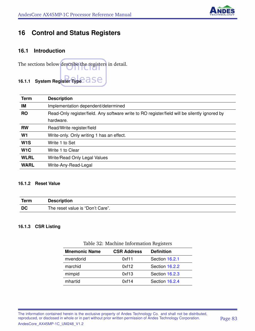
AndesCore AX45MP-1C Processor Reference Manual
16 Control and Status Registers
16.1 Introduction
The sections below describe the registers in detail.
16.1.1 System Register Type
Term Description
IM Implementation dependent/determined
RO Read-Only register/field. Any software write to RO register/field will be silently ignored byhardware.
RW Read/Write register/field
W1 Write-only. Only writing 1 has an effect.
W1S Write 1 to Set
W1C Write 1 to Clear
WLRL Write/Read Only Legal Values
WARL Write-Any-Read-Legal
16.1.2 Reset Value
Term Description
DC The reset value is “Don’t Care”.
16.1.3 CSR Listing
Table 32: Machine Information Registers
Mnemonic Name CSR Address Definition
mvendorid 0xf11 Section 16.2.1
marchid 0xf12 Section 16.2.2
mimpid 0xf13 Section 16.2.3
mhartid 0xf14 Section 16.2.4
The information contained herein is the exclusive property of Andes Technology Co. and shall not be distributed,reproduced, or disclosed in whole or in part without prior written permission of Andes Technology Corporation.AndesCore_AX45MP-1C_UM248_V1.2
Page 83
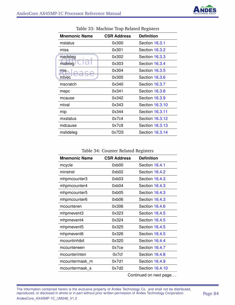
AndesCore AX45MP-1C Processor Reference Manual
Table 33: Machine Trap Related Registers
Mnemonic Name CSR Address Definition
mstatus 0x300 Section 16.3.1
misa 0x301 Section 16.3.2
medeleg 0x302 Section 16.3.3
mideleg 0x303 Section 16.3.4
mie 0x304 Section 16.3.5
mtvec 0x305 Section 16.3.6
mscratch 0x340 Section 16.3.7
mepc 0x341 Section 16.3.8
mcause 0x342 Section 16.3.9
mtval 0x343 Section 16.3.10
mip 0x344 Section 16.3.11
mxstatus 0x7c4 Section 16.3.12
mdcause 0x7c9 Section 16.3.13
mslideleg 0x7D5 Section 16.3.14
Table 34: Counter Related Registers
Mnemonic Name CSR Address Definition
mcycle 0xb00 Section 16.4.1
minstret 0xb02 Section 16.4.2
mhpmcounter3 0xb03 Section 16.4.3
mhpmcounter4 0xb04 Section 16.4.3
mhpmcounter5 0xb05 Section 16.4.3
mhpmcounter6 0xb06 Section 16.4.3
mcounteren 0x306 Section 16.4.6
mhpmevent3 0x323 Section 16.4.5
mhpmevent4 0x324 Section 16.4.5
mhpmevent5 0x325 Section 16.4.5
mhpmevent6 0x326 Section 16.4.5
mcountinhibit 0x320 Section 16.4.4
mcounterwen 0x7ce Section 16.4.7
mcounterinten 0x7cf Section 16.4.8
mcountermask_m 0x7d1 Section 16.4.9
mcountermask_s 0x7d2 Section 16.4.10
Continued on next page. . .
The information contained herein is the exclusive property of Andes Technology Co. and shall not be distributed,reproduced, or disclosed in whole or in part without prior written permission of Andes Technology Corporation.AndesCore_AX45MP-1C_UM248_V1.2
Page 84
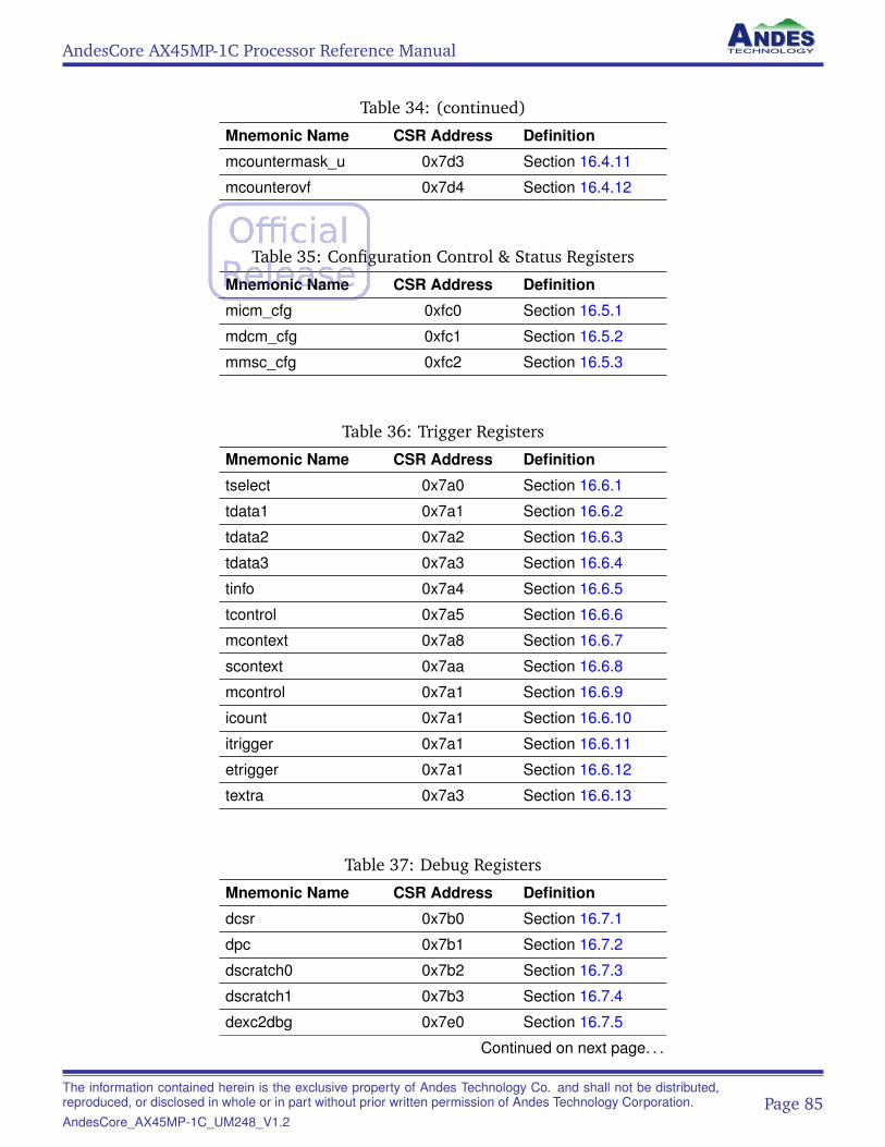
AndesCore AX45MP-1C Processor Reference Manual
Table 34: (continued)
Mnemonic Name CSR Address Definition
mcountermask_u 0x7d3 Section 16.4.11
mcounterovf 0x7d4 Section 16.4.12
Table 35: Configuration Control & Status Registers
Mnemonic Name CSR Address Definition
micm_cfg 0xfc0 Section 16.5.1
mdcm_cfg 0xfc1 Section 16.5.2
mmsc_cfg 0xfc2 Section 16.5.3
Table 36: Trigger Registers
Mnemonic Name CSR Address Definition
tselect 0x7a0 Section 16.6.1
tdata1 0x7a1 Section 16.6.2
tdata2 0x7a2 Section 16.6.3
tdata3 0x7a3 Section 16.6.4
tinfo 0x7a4 Section 16.6.5
tcontrol 0x7a5 Section 16.6.6
mcontext 0x7a8 Section 16.6.7
scontext 0x7aa Section 16.6.8
mcontrol 0x7a1 Section 16.6.9
icount 0x7a1 Section 16.6.10
itrigger 0x7a1 Section 16.6.11
etrigger 0x7a1 Section 16.6.12
textra 0x7a3 Section 16.6.13
Table 37: Debug Registers
Mnemonic Name CSR Address Definition
dcsr 0x7b0 Section 16.7.1
dpc 0x7b1 Section 16.7.2
dscratch0 0x7b2 Section 16.7.3
dscratch1 0x7b3 Section 16.7.4
dexc2dbg 0x7e0 Section 16.7.5
Continued on next page. . .
The information contained herein is the exclusive property of Andes Technology Co. and shall not be distributed,reproduced, or disclosed in whole or in part without prior written permission of Andes Technology Corporation.AndesCore_AX45MP-1C_UM248_V1.2
Page 85
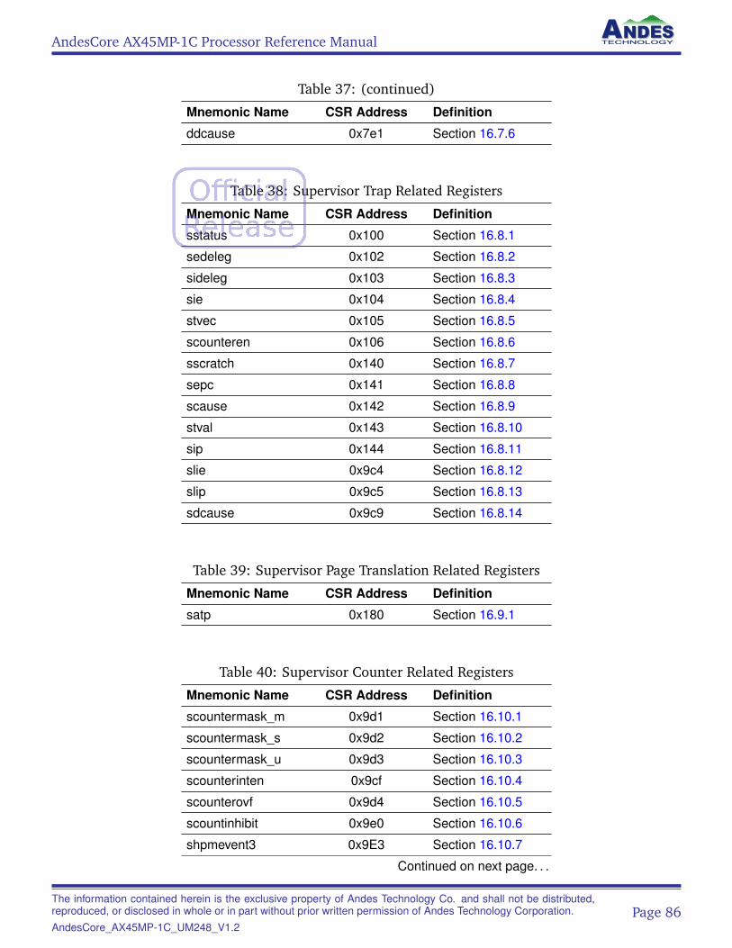
AndesCore AX45MP-1C Processor Reference Manual
Table 37: (continued)
Mnemonic Name CSR Address Definition
ddcause 0x7e1 Section 16.7.6
Table 38: Supervisor Trap Related Registers
Mnemonic Name CSR Address Definition
sstatus 0x100 Section 16.8.1
sedeleg 0x102 Section 16.8.2
sideleg 0x103 Section 16.8.3
sie 0x104 Section 16.8.4
stvec 0x105 Section 16.8.5
scounteren 0x106 Section 16.8.6
sscratch 0x140 Section 16.8.7
sepc 0x141 Section 16.8.8
scause 0x142 Section 16.8.9
stval 0x143 Section 16.8.10
sip 0x144 Section 16.8.11
slie 0x9c4 Section 16.8.12
slip 0x9c5 Section 16.8.13
sdcause 0x9c9 Section 16.8.14
Table 39: Supervisor Page Translation Related Registers
Mnemonic Name CSR Address Definition
satp 0x180 Section 16.9.1
Table 40: Supervisor Counter Related Registers
Mnemonic Name CSR Address Definition
scountermask_m 0x9d1 Section 16.10.1
scountermask_s 0x9d2 Section 16.10.2
scountermask_u 0x9d3 Section 16.10.3
scounterinten 0x9cf Section 16.10.4
scounterovf 0x9d4 Section 16.10.5
scountinhibit 0x9e0 Section 16.10.6
shpmevent3 0x9E3 Section 16.10.7
Continued on next page. . .
The information contained herein is the exclusive property of Andes Technology Co. and shall not be distributed,reproduced, or disclosed in whole or in part without prior written permission of Andes Technology Corporation.AndesCore_AX45MP-1C_UM248_V1.2
Page 86
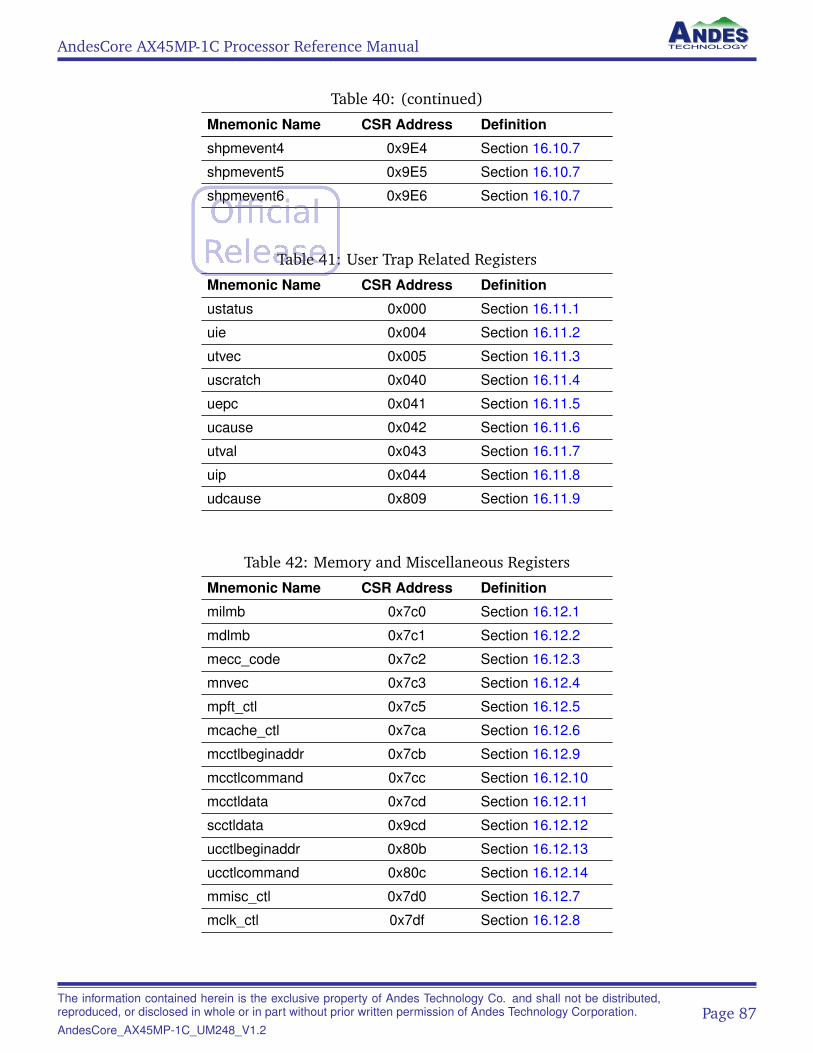
AndesCore AX45MP-1C Processor Reference Manual
Table 40: (continued)
Mnemonic Name CSR Address Definition
shpmevent4 0x9E4 Section 16.10.7
shpmevent5 0x9E5 Section 16.10.7
shpmevent6 0x9E6 Section 16.10.7
Table 41: User Trap Related Registers
Mnemonic Name CSR Address Definition
ustatus 0x000 Section 16.11.1
uie 0x004 Section 16.11.2
utvec 0x005 Section 16.11.3
uscratch 0x040 Section 16.11.4
uepc 0x041 Section 16.11.5
ucause 0x042 Section 16.11.6
utval 0x043 Section 16.11.7
uip 0x044 Section 16.11.8
udcause 0x809 Section 16.11.9
Table 42: Memory and Miscellaneous Registers
Mnemonic Name CSR Address Definition
milmb 0x7c0 Section 16.12.1
mdlmb 0x7c1 Section 16.12.2
mecc_code 0x7c2 Section 16.12.3
mnvec 0x7c3 Section 16.12.4
mpft_ctl 0x7c5 Section 16.12.5
mcache_ctl 0x7ca Section 16.12.6
mcctlbeginaddr 0x7cb Section 16.12.9
mcctlcommand 0x7cc Section 16.12.10
mcctldata 0x7cd Section 16.12.11
scctldata 0x9cd Section 16.12.12
ucctlbeginaddr 0x80b Section 16.12.13
ucctlcommand 0x80c Section 16.12.14
mmisc_ctl 0x7d0 Section 16.12.7
mclk_ctl 0x7df Section 16.12.8
The information contained herein is the exclusive property of Andes Technology Co. and shall not be distributed,reproduced, or disclosed in whole or in part without prior written permission of Andes Technology Corporation.AndesCore_AX45MP-1C_UM248_V1.2
Page 87
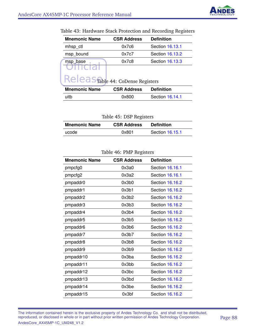
AndesCore AX45MP-1C Processor Reference Manual
Table 43: Hardware Stack Protection and Recording Registers
Mnemonic Name CSR Address Definition
mhsp_ctl 0x7c6 Section 16.13.1
msp_bound 0x7c7 Section 16.13.2
msp_base 0x7c8 Section 16.13.3
Table 44: CoDense Registers
Mnemonic Name CSR Address Definition
uitb 0x800 Section 16.14.1
Table 45: DSP Registers
Mnemonic Name CSR Address Definition
ucode 0x801 Section 16.15.1
Table 46: PMP Registers
Mnemonic Name CSR Address Definition
pmpcfg0 0x3a0 Section 16.16.1
pmpcfg2 0x3a2 Section 16.16.1
pmpaddr0 0x3b0 Section 16.16.2
pmpaddr1 0x3b1 Section 16.16.2
pmpaddr2 0x3b2 Section 16.16.2
pmpaddr3 0x3b3 Section 16.16.2
pmpaddr4 0x3b4 Section 16.16.2
pmpaddr5 0x3b5 Section 16.16.2
pmpaddr6 0x3b6 Section 16.16.2
pmpaddr7 0x3b7 Section 16.16.2
pmpaddr8 0x3b8 Section 16.16.2
pmpaddr9 0x3b9 Section 16.16.2
pmpaddr10 0x3ba Section 16.16.2
pmpaddr11 0x3bb Section 16.16.2
pmpaddr12 0x3bc Section 16.16.2
pmpaddr13 0x3bd Section 16.16.2
pmpaddr14 0x3be Section 16.16.2
pmpaddr15 0x3bf Section 16.16.2
The information contained herein is the exclusive property of Andes Technology Co. and shall not be distributed,reproduced, or disclosed in whole or in part without prior written permission of Andes Technology Corporation.AndesCore_AX45MP-1C_UM248_V1.2
Page 88
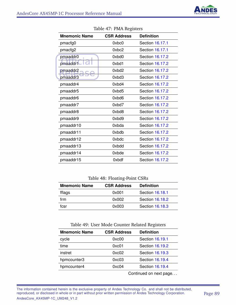
AndesCore AX45MP-1C Processor Reference Manual
Table 47: PMA Registers
Mnemonic Name CSR Address Definition
pmacfg0 0xbc0 Section 16.17.1
pmacfg2 0xbc2 Section 16.17.1
pmaaddr0 0xbd0 Section 16.17.2
pmaaddr1 0xbd1 Section 16.17.2
pmaaddr2 0xbd2 Section 16.17.2
pmaaddr3 0xbd3 Section 16.17.2
pmaaddr4 0xbd4 Section 16.17.2
pmaaddr5 0xbd5 Section 16.17.2
pmaaddr6 0xbd6 Section 16.17.2
pmaaddr7 0xbd7 Section 16.17.2
pmaaddr8 0xbd8 Section 16.17.2
pmaaddr9 0xbd9 Section 16.17.2
pmaaddr10 0xbda Section 16.17.2
pmaaddr11 0xbdb Section 16.17.2
pmaaddr12 0xbdc Section 16.17.2
pmaaddr13 0xbdd Section 16.17.2
pmaaddr14 0xbde Section 16.17.2
pmaaddr15 0xbdf Section 16.17.2
Table 48: Floating-Point CSRs
Mnemonic Name CSR Address Definition
fflags 0x001 Section 16.18.1
frm 0x002 Section 16.18.2
fcsr 0x003 Section 16.18.3
Table 49: User Mode Counter Related Registers
Mnemonic Name CSR Address Definition
cycle 0xc00 Section 16.19.1
time 0xc01 Section 16.19.2
instret 0xc02 Section 16.19.3
hpmcounter3 0xc03 Section 16.19.4
hpmcounter4 0xc04 Section 16.19.4
Continued on next page. . .
The information contained herein is the exclusive property of Andes Technology Co. and shall not be distributed,reproduced, or disclosed in whole or in part without prior written permission of Andes Technology Corporation.AndesCore_AX45MP-1C_UM248_V1.2
Page 89
AndesCore AX45MP-1C Processor Reference Manual
Table 49: (continued)
Mnemonic Name CSR Address Definition
hpmcounter5 0xc05 Section 16.19.4
hpmcounter6 0xc06 Section 16.19.4
The information contained herein is the exclusive property of Andes Technology Co. and shall not be distributed,reproduced, or disclosed in whole or in part without prior written permission of Andes Technology Corporation.AndesCore_AX45MP-1C_UM248_V1.2
Page 90
AndesCore AX45MP-1C Processor Reference Manual
16.2 Machine Information Registers
16.2.1 Machine Vendor ID Register
Mnemonic Name: mvendoridIM Requirement: RequiredAccess Mode: MachineCSR Address: 0xf11 (standard read only)
63 0
MVENDORID
This read-only register provides the Andes JEDEC manufacturer ID: 0x0000031e.
Field Name Bits Description Type Reset
MVENDORID [63:0] The manufacturer ID of Andes RO 0x0000031e
16.2.2 Machine Architecture ID Register
Mnemonic Name: marchidIM Requirement: RequiredAccess Mode: MachineCSR Address: 0xf12 (standard read only)
63
1
62 31
0
30 0
CPU_ID
This register provides the micro-architecture id of AndesCore processor implementations. For AX45MP-1C, marchid.CPU_ID will be 0x8a45. Note that the MSB of this register is 1 for commercial imple-mentations of RISC-V processors.
Field Name Bits Description Type Reset
CPU_ID [30:0] Andes CPU ID RO 0x8a45
The information contained herein is the exclusive property of Andes Technology Co. and shall not be distributed,reproduced, or disclosed in whole or in part without prior written permission of Andes Technology Corporation.AndesCore_AX45MP-1C_UM248_V1.2
Page 91
AndesCore AX45MP-1C Processor Reference Manual
16.2.3 Machine Implementation ID Register
Mnemonic Name: mimpidIM Requirement: RequiredAccess Mode: MachineCSR Address: 0xf13 (standard read only)
63 32
0
31 8
MAJOR
7 4
MINOR
3 0
EXTENSION
This register is used to identify the revision number of the processor, which is denoted using theMAJOR.MINOR.EXTENSION format.
Field Name Bits Description Type Reset
EXTENSION [3:0] Revision extension RO IM
MINOR [7:4] Revision minor RO IM
MAJOR [31:8] Revision major RO IM
The information contained herein is the exclusive property of Andes Technology Co. and shall not be distributed,reproduced, or disclosed in whole or in part without prior written permission of Andes Technology Corporation.AndesCore_AX45MP-1C_UM248_V1.2
Page 92
AndesCore AX45MP-1C Processor Reference Manual
16.2.4 Hart ID Register
Mnemonic Name: mhartidIM Requirement: RequiredAccess Mode: MachineCSR Address: 0xf14 (standard read only)
63 0
MHARTID
This register provides the ID of the hardware thread. It is required that one of the hart IDs must bezero on a RISC-V platform.
16.3 Machine Trap Related CSRs
16.3.1 Machine Status
Mnemonic Name: mstatusIM Requirement: RequiredAccess Mode: MachineCSR Address: 0x300 (standard read/write)
63
SD
62 36
0
35 34
SXL
33 32
UXL
31 25
0
24 23
0
22
TSR
21
TW
20
TVM
19
MXR
18
SUM
17
MPRV
16 15
0
14 13
FS
12 11
MPP
10 9
0
8
SPP
7
MPIE
6
0
5
SPIE
4
UPIE
3
MIE
2
0
1
SIE
0
UIE
Field Name Bits Description Type Reset
UIE [0] U-mode interrupt enable bit.
Value Meaning
0 Disabled
1 Enabled
RW 0
SIE [1] S-mode interrupt enable bit.
Value Meaning
0 Disabled
1 Enabled
RW 0
Continued on next page. . .
The information contained herein is the exclusive property of Andes Technology Co. and shall not be distributed,reproduced, or disclosed in whole or in part without prior written permission of Andes Technology Corporation.AndesCore_AX45MP-1C_UM248_V1.2
Page 93
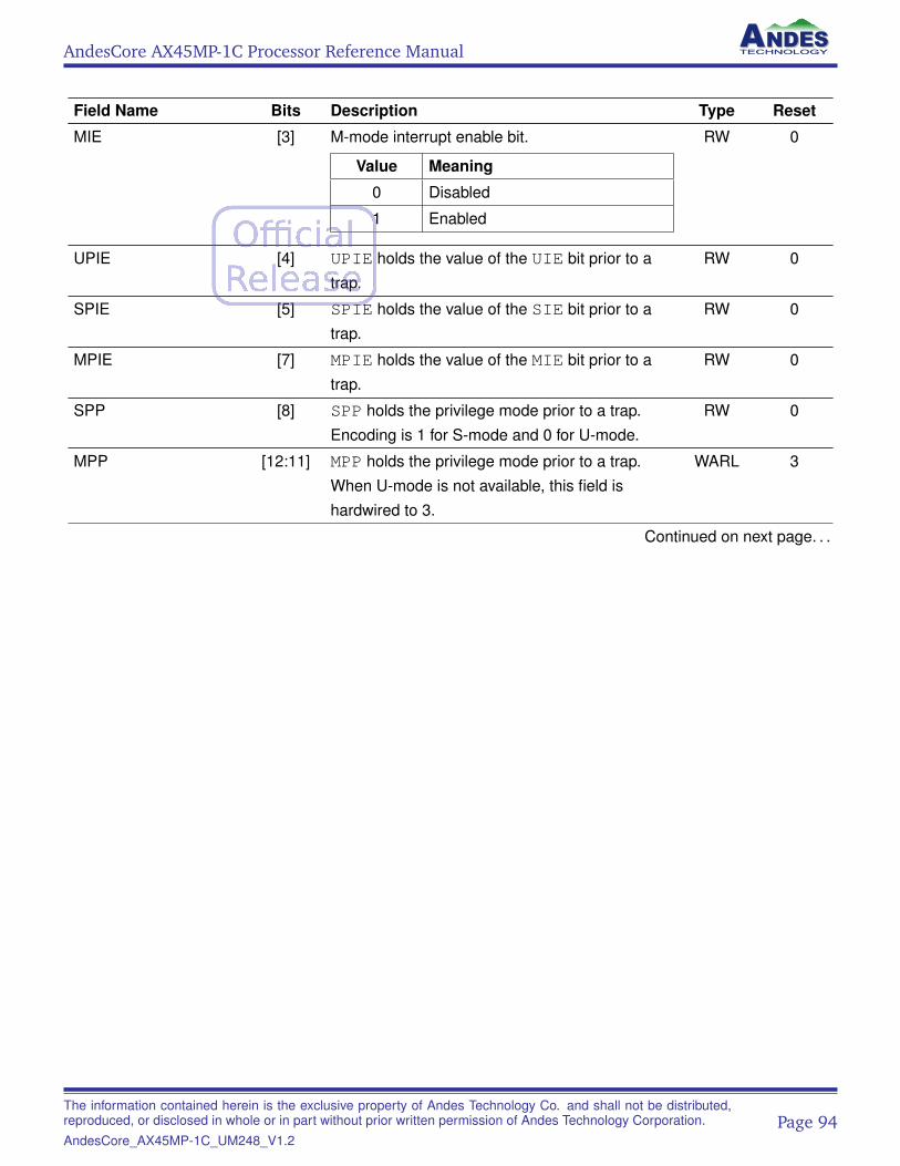
AndesCore AX45MP-1C Processor Reference Manual
Field Name Bits Description Type Reset
MIE [3] M-mode interrupt enable bit.
Value Meaning
0 Disabled
1 Enabled
RW 0
UPIE [4] UPIE holds the value of the UIE bit prior to atrap.
RW 0
SPIE [5] SPIE holds the value of the SIE bit prior to atrap.
RW 0
MPIE [7] MPIE holds the value of the MIE bit prior to atrap.
RW 0
SPP [8] SPP holds the privilege mode prior to a trap.Encoding is 1 for S-mode and 0 for U-mode.
RW 0
MPP [12:11] MPP holds the privilege mode prior to a trap.When U-mode is not available, this field ishardwired to 3.
WARL 3
Continued on next page. . .
The information contained herein is the exclusive property of Andes Technology Co. and shall not be distributed,reproduced, or disclosed in whole or in part without prior written permission of Andes Technology Corporation.AndesCore_AX45MP-1C_UM248_V1.2
Page 94
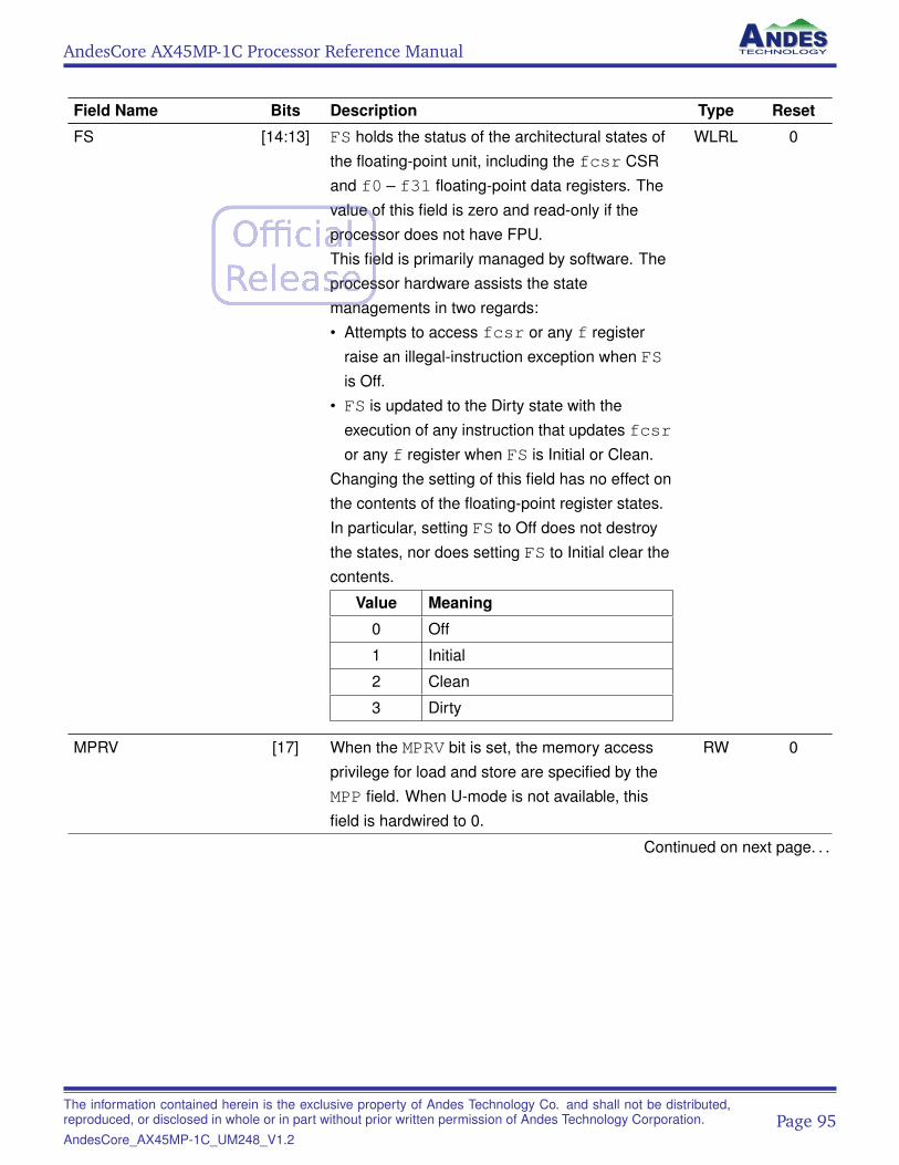
AndesCore AX45MP-1C Processor Reference Manual
Field Name Bits Description Type Reset
FS [14:13] FS holds the status of the architectural states ofthe floating-point unit, including the fcsr CSRand f0 – f31 floating-point data registers. Thevalue of this field is zero and read-only if theprocessor does not have FPU.This field is primarily managed by software. Theprocessor hardware assists the statemanagements in two regards:• Attempts to access fcsr or any f register
raise an illegal-instruction exception when FSis Off.
• FS is updated to the Dirty state with theexecution of any instruction that updates fcsror any f register when FS is Initial or Clean.
Changing the setting of this field has no effect onthe contents of the floating-point register states.In particular, setting FS to Off does not destroythe states, nor does setting FS to Initial clear thecontents.
Value Meaning
0 Off
1 Initial
2 Clean
3 Dirty
WLRL 0
MPRV [17] When the MPRV bit is set, the memory accessprivilege for load and store are specified by theMPP field. When U-mode is not available, thisfield is hardwired to 0.
RW 0
Continued on next page. . .
The information contained herein is the exclusive property of Andes Technology Co. and shall not be distributed,reproduced, or disclosed in whole or in part without prior written permission of Andes Technology Corporation.AndesCore_AX45MP-1C_UM248_V1.2
Page 95
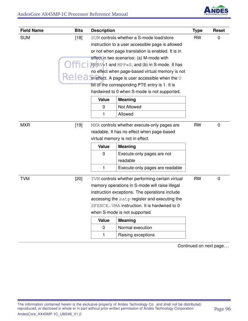
AndesCore AX45MP-1C Processor Reference Manual
Field Name Bits Description Type Reset
SUM [18] SUM controls whether a S-mode load/storeinstruction to a user accessible page is allowedor not when page translation is enabled. It is ineffect in two scenarios: (a) M-mode withMPRV=1 and MPP=S, and (b) in S-mode. It hasno effect when page-based virtual memory is notin effect. A page is user accessible when the Ubit of the corresponding PTE entry is 1. It ishardwired to 0 when S-mode is not supported.
Value Meaning
0 Not Allowed
1 Allowed
RW 0
MXR [19] MXR controls whether execute-only pages arereadable. It has no effect when page-basedvirtual memory is not in effect.
Value Meaning
0 Execute-only pages are notreadable
1 Execute-only pages are readable
RW 0
TVM [20] TVM controls whether performing certain virtualmemory operations in S-mode will raise illegalinstruction exceptions. The operations includeaccessing the satp register and executing theSFENCE.VMA instruction. It is hardwired to 0when S-mode is not supported.
Value Meaning
0 Normal execution
1 Raising exceptions
RW 0
Continued on next page. . .
The information contained herein is the exclusive property of Andes Technology Co. and shall not be distributed,reproduced, or disclosed in whole or in part without prior written permission of Andes Technology Corporation.AndesCore_AX45MP-1C_UM248_V1.2
Page 96
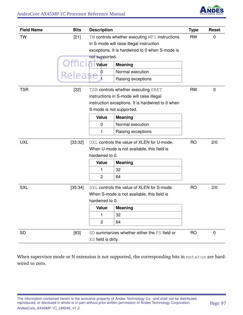
AndesCore AX45MP-1C Processor Reference Manual
Field Name Bits Description Type Reset
TW [21] TW controls whether executing WFI instructionsin S-mode will raise illegal instructionexceptions. It is hardwired to 0 when S-mode isnot supported.
Value Meaning
0 Normal execution
1 Raising exceptions
RW 0
TSR [22] TSR controls whether executing SRETinstructions in S-mode will raise illegalinstruction exceptions. It is hardwired to 0 whenS-mode is not supported.
Value Meaning
0 Normal execution
1 Raising exceptions
RW 0
UXL [33:32] UXL controls the value of XLEN for U-mode.When U-mode is not available, this field ishardwired to 0.
Value Meaning
1 32
2 64
RO 2/0
SXL [35:34] SXL controls the value of XLEN for S-mode.When S-mode is not available, this field ishardwired to 0.
Value Meaning
1 32
2 64
RO 2/0
SD [63] SD summarizes whether either the FS field orXS field is dirty.
RO 0
When supervisor mode or N extension is not supported, the corresponding bits in mstatus are hard-wired to zero.
The information contained herein is the exclusive property of Andes Technology Co. and shall not be distributed,reproduced, or disclosed in whole or in part without prior written permission of Andes Technology Corporation.AndesCore_AX45MP-1C_UM248_V1.2
Page 97
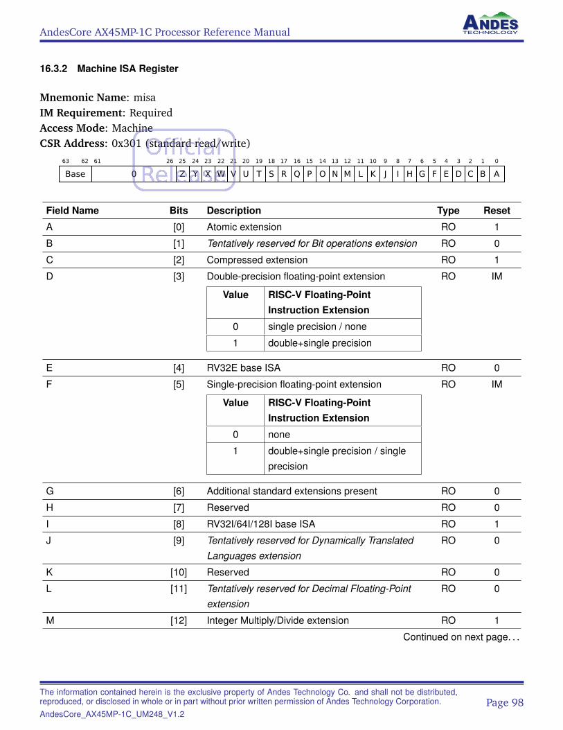
AndesCore AX45MP-1C Processor Reference Manual
16.3.2 Machine ISA Register
Mnemonic Name: misaIM Requirement: RequiredAccess Mode: MachineCSR Address: 0x301 (standard read/write)
63 62
Base
61 26
0
25
Z
24
Y
23
X
22
W
21
V
20
U
19
T
18
S
17
R
16
Q
15
P
14
O
13
N
12
M
11
L
10
K
9
J
8
I
7
H
6
G
5
F
4
E
3
D
2
C
1
B
0
A
Field Name Bits Description Type Reset
A [0] Atomic extension RO 1
B [1] Tentatively reserved for Bit operations extension RO 0
C [2] Compressed extension RO 1
D [3] Double-precision floating-point extension
Value RISC-V Floating-PointInstruction Extension
0 single precision / none
1 double+single precision
RO IM
E [4] RV32E base ISA RO 0
F [5] Single-precision floating-point extension
Value RISC-V Floating-PointInstruction Extension
0 none
1 double+single precision / singleprecision
RO IM
G [6] Additional standard extensions present RO 0
H [7] Reserved RO 0
I [8] RV32I/64I/128I base ISA RO 1
J [9] Tentatively reserved for Dynamically TranslatedLanguages extension
RO 0
K [10] Reserved RO 0
L [11] Tentatively reserved for Decimal Floating-Pointextension
RO 0
M [12] Integer Multiply/Divide extension RO 1
Continued on next page. . .
The information contained herein is the exclusive property of Andes Technology Co. and shall not be distributed,reproduced, or disclosed in whole or in part without prior written permission of Andes Technology Corporation.AndesCore_AX45MP-1C_UM248_V1.2
Page 98
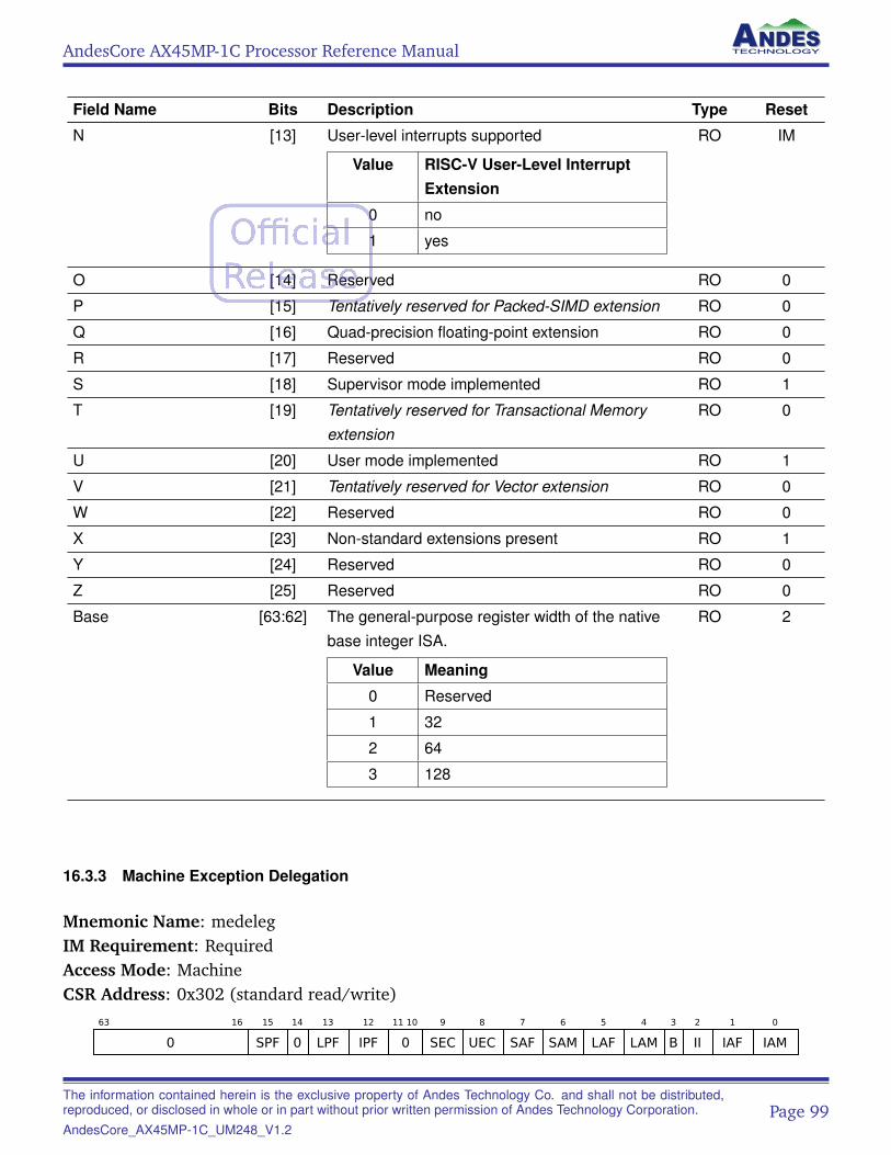
AndesCore AX45MP-1C Processor Reference Manual
Field Name Bits Description Type Reset
N [13] User-level interrupts supported
Value RISC-V User-Level InterruptExtension
0 no
1 yes
RO IM
O [14] Reserved RO 0
P [15] Tentatively reserved for Packed-SIMD extension RO 0
Q [16] Quad-precision floating-point extension RO 0
R [17] Reserved RO 0
S [18] Supervisor mode implemented RO 1
T [19] Tentatively reserved for Transactional Memoryextension
RO 0
U [20] User mode implemented RO 1
V [21] Tentatively reserved for Vector extension RO 0
W [22] Reserved RO 0
X [23] Non-standard extensions present RO 1
Y [24] Reserved RO 0
Z [25] Reserved RO 0
Base [63:62] The general-purpose register width of the nativebase integer ISA.
Value Meaning
0 Reserved
1 32
2 64
3 128
RO 2
16.3.3 Machine Exception Delegation
Mnemonic Name: medelegIM Requirement: RequiredAccess Mode: MachineCSR Address: 0x302 (standard read/write)
63 16
0
15
SPF
14
0
13
LPF
12
IPF
11 10
0
9
SEC
8
UEC
7
SAF
6
SAM
5
LAF
4
LAM
3
B
2
II
1
IAF
0
IAM
The information contained herein is the exclusive property of Andes Technology Co. and shall not be distributed,reproduced, or disclosed in whole or in part without prior written permission of Andes Technology Corporation.AndesCore_AX45MP-1C_UM248_V1.2
Page 99
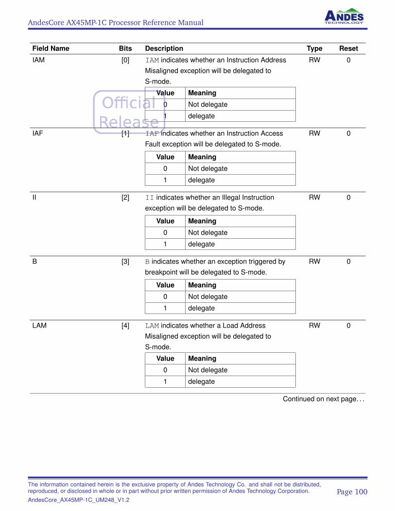
AndesCore AX45MP-1C Processor Reference Manual
Field Name Bits Description Type Reset
IAM [0] IAM indicates whether an Instruction AddressMisaligned exception will be delegated toS-mode.
Value Meaning
0 Not delegate
1 delegate
RW 0
IAF [1] IAF indicates whether an Instruction AccessFault exception will be delegated to S-mode.
Value Meaning
0 Not delegate
1 delegate
RW 0
II [2] II indicates whether an Illegal Instructionexception will be delegated to S-mode.
Value Meaning
0 Not delegate
1 delegate
RW 0
B [3] B indicates whether an exception triggered bybreakpoint will be delegated to S-mode.
Value Meaning
0 Not delegate
1 delegate
RW 0
LAM [4] LAM indicates whether a Load AddressMisaligned exception will be delegated toS-mode.
Value Meaning
0 Not delegate
1 delegate
RW 0
Continued on next page. . .
The information contained herein is the exclusive property of Andes Technology Co. and shall not be distributed,reproduced, or disclosed in whole or in part without prior written permission of Andes Technology Corporation.AndesCore_AX45MP-1C_UM248_V1.2
Page 100
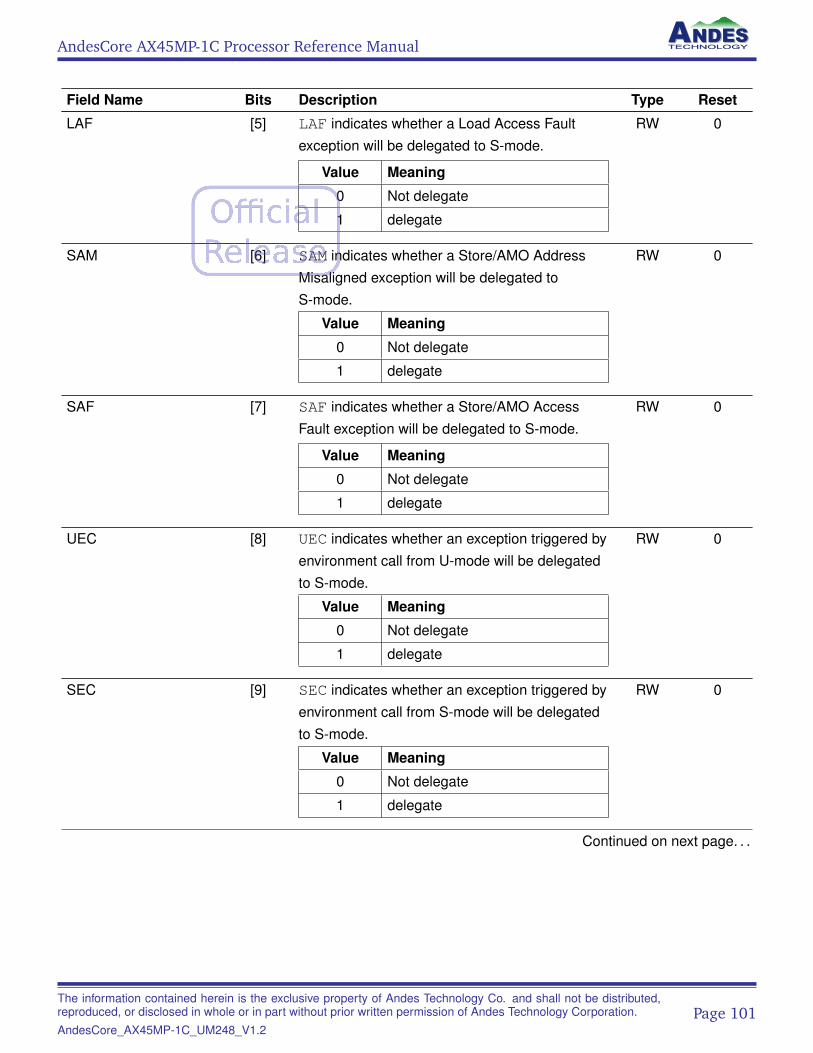
AndesCore AX45MP-1C Processor Reference Manual
Field Name Bits Description Type Reset
LAF [5] LAF indicates whether a Load Access Faultexception will be delegated to S-mode.
Value Meaning
0 Not delegate
1 delegate
RW 0
SAM [6] SAM indicates whether a Store/AMO AddressMisaligned exception will be delegated toS-mode.
Value Meaning
0 Not delegate
1 delegate
RW 0
SAF [7] SAF indicates whether a Store/AMO AccessFault exception will be delegated to S-mode.
Value Meaning
0 Not delegate
1 delegate
RW 0
UEC [8] UEC indicates whether an exception triggered byenvironment call from U-mode will be delegatedto S-mode.
Value Meaning
0 Not delegate
1 delegate
RW 0
SEC [9] SEC indicates whether an exception triggered byenvironment call from S-mode will be delegatedto S-mode.
Value Meaning
0 Not delegate
1 delegate
RW 0
Continued on next page. . .
The information contained herein is the exclusive property of Andes Technology Co. and shall not be distributed,reproduced, or disclosed in whole or in part without prior written permission of Andes Technology Corporation.AndesCore_AX45MP-1C_UM248_V1.2
Page 101
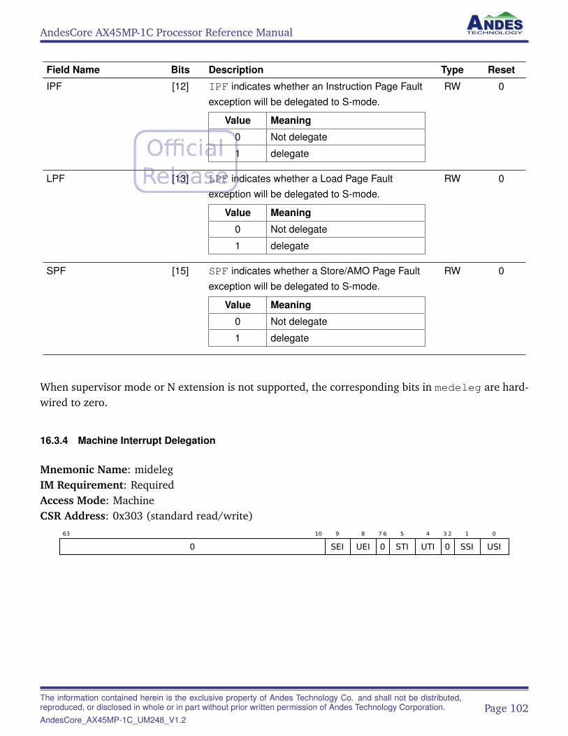
AndesCore AX45MP-1C Processor Reference Manual
Field Name Bits Description Type Reset
IPF [12] IPF indicates whether an Instruction Page Faultexception will be delegated to S-mode.
Value Meaning
0 Not delegate
1 delegate
RW 0
LPF [13] LPF indicates whether a Load Page Faultexception will be delegated to S-mode.
Value Meaning
0 Not delegate
1 delegate
RW 0
SPF [15] SPF indicates whether a Store/AMO Page Faultexception will be delegated to S-mode.
Value Meaning
0 Not delegate
1 delegate
RW 0
When supervisor mode or N extension is not supported, the corresponding bits in medeleg are hard-wired to zero.
16.3.4 Machine Interrupt Delegation
Mnemonic Name: midelegIM Requirement: RequiredAccess Mode: MachineCSR Address: 0x303 (standard read/write)
63 10
0
9
SEI
8
UEI
7 6
0
5
STI
4
UTI
3 2
0
1
SSI
0
USI
The information contained herein is the exclusive property of Andes Technology Co. and shall not be distributed,reproduced, or disclosed in whole or in part without prior written permission of Andes Technology Corporation.AndesCore_AX45MP-1C_UM248_V1.2
Page 102
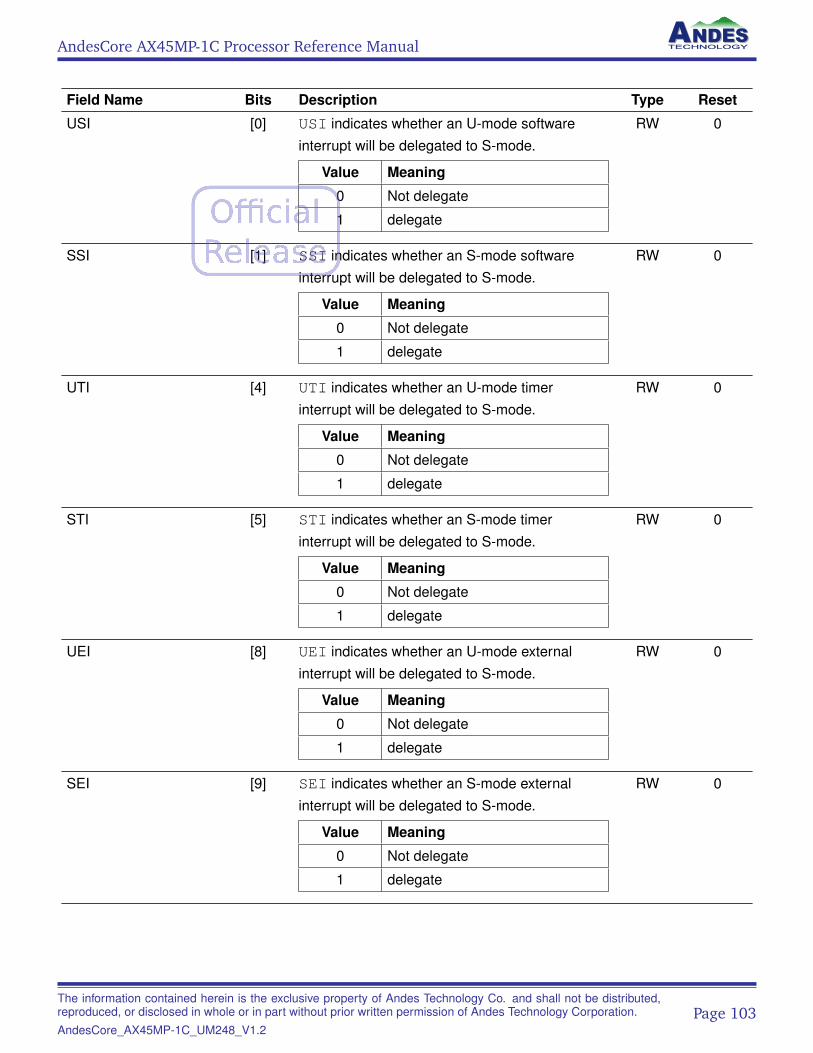
AndesCore AX45MP-1C Processor Reference Manual
Field Name Bits Description Type Reset
USI [0] USI indicates whether an U-mode softwareinterrupt will be delegated to S-mode.
Value Meaning
0 Not delegate
1 delegate
RW 0
SSI [1] SSI indicates whether an S-mode softwareinterrupt will be delegated to S-mode.
Value Meaning
0 Not delegate
1 delegate
RW 0
UTI [4] UTI indicates whether an U-mode timerinterrupt will be delegated to S-mode.
Value Meaning
0 Not delegate
1 delegate
RW 0
STI [5] STI indicates whether an S-mode timerinterrupt will be delegated to S-mode.
Value Meaning
0 Not delegate
1 delegate
RW 0
UEI [8] UEI indicates whether an U-mode externalinterrupt will be delegated to S-mode.
Value Meaning
0 Not delegate
1 delegate
RW 0
SEI [9] SEI indicates whether an S-mode externalinterrupt will be delegated to S-mode.
Value Meaning
0 Not delegate
1 delegate
RW 0
The information contained herein is the exclusive property of Andes Technology Co. and shall not be distributed,reproduced, or disclosed in whole or in part without prior written permission of Andes Technology Corporation.AndesCore_AX45MP-1C_UM248_V1.2
Page 103
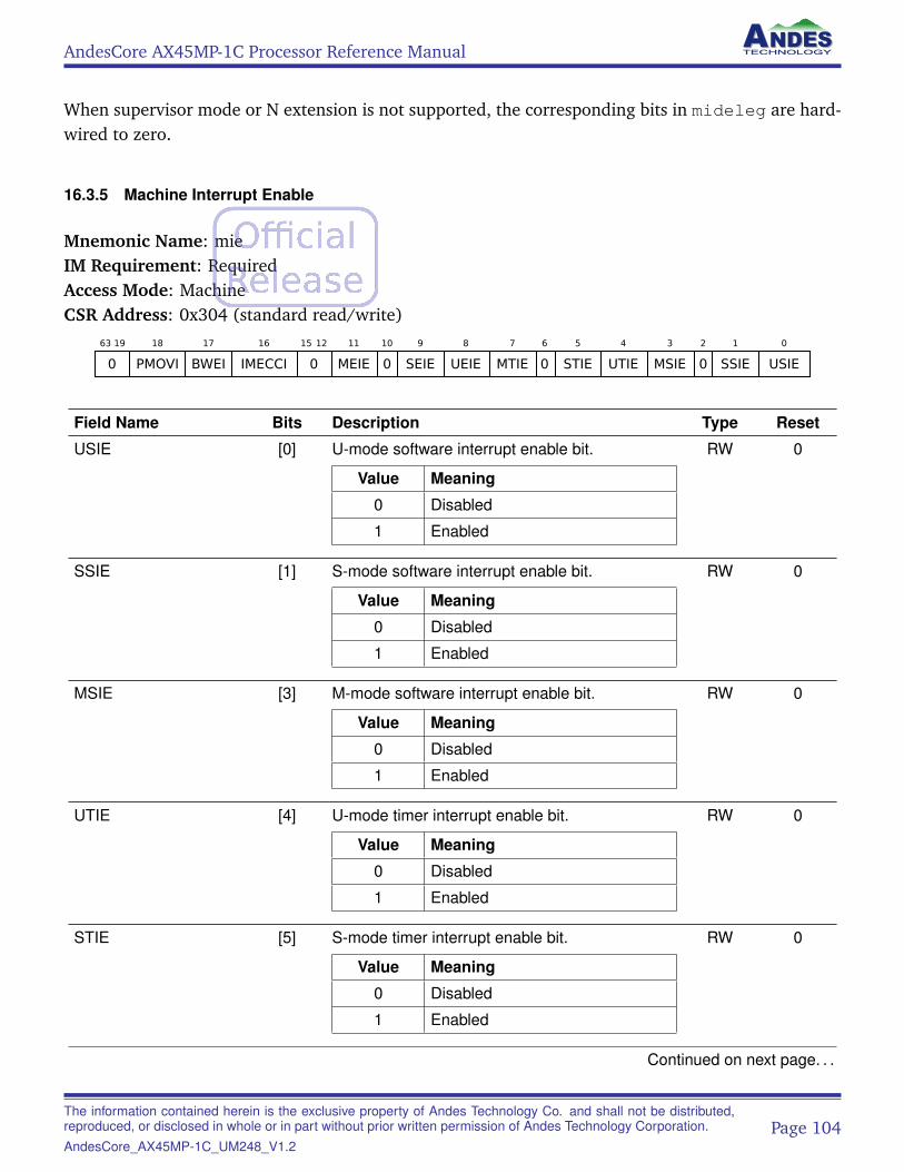
AndesCore AX45MP-1C Processor Reference Manual
When supervisor mode or N extension is not supported, the corresponding bits in mideleg are hard-wired to zero.
16.3.5 Machine Interrupt Enable
Mnemonic Name: mieIM Requirement: RequiredAccess Mode: MachineCSR Address: 0x304 (standard read/write)
63 19
0
18
PMOVI
17
BWEI
16
IMECCI
15 12
0
11
MEIE
10
0
9
SEIE
8
UEIE
7
MTIE
6
0
5
STIE
4
UTIE
3
MSIE
2
0
1
SSIE
0
USIE
Field Name Bits Description Type Reset
USIE [0] U-mode software interrupt enable bit.
Value Meaning
0 Disabled
1 Enabled
RW 0
SSIE [1] S-mode software interrupt enable bit.
Value Meaning
0 Disabled
1 Enabled
RW 0
MSIE [3] M-mode software interrupt enable bit.
Value Meaning
0 Disabled
1 Enabled
RW 0
UTIE [4] U-mode timer interrupt enable bit.
Value Meaning
0 Disabled
1 Enabled
RW 0
STIE [5] S-mode timer interrupt enable bit.
Value Meaning
0 Disabled
1 Enabled
RW 0
Continued on next page. . .
The information contained herein is the exclusive property of Andes Technology Co. and shall not be distributed,reproduced, or disclosed in whole or in part without prior written permission of Andes Technology Corporation.AndesCore_AX45MP-1C_UM248_V1.2
Page 104
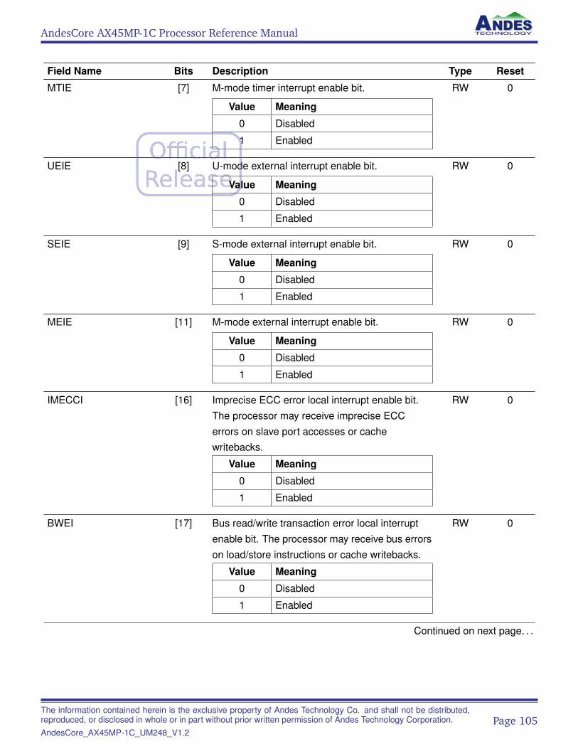
AndesCore AX45MP-1C Processor Reference Manual
Field Name Bits Description Type Reset
MTIE [7] M-mode timer interrupt enable bit.
Value Meaning
0 Disabled
1 Enabled
RW 0
UEIE [8] U-mode external interrupt enable bit.
Value Meaning
0 Disabled
1 Enabled
RW 0
SEIE [9] S-mode external interrupt enable bit.
Value Meaning
0 Disabled
1 Enabled
RW 0
MEIE [11] M-mode external interrupt enable bit.
Value Meaning
0 Disabled
1 Enabled
RW 0
IMECCI [16] Imprecise ECC error local interrupt enable bit.The processor may receive imprecise ECCerrors on slave port accesses or cachewritebacks.
Value Meaning
0 Disabled
1 Enabled
RW 0
BWEI [17] Bus read/write transaction error local interruptenable bit. The processor may receive bus errorson load/store instructions or cache writebacks.
Value Meaning
0 Disabled
1 Enabled
RW 0
Continued on next page. . .
The information contained herein is the exclusive property of Andes Technology Co. and shall not be distributed,reproduced, or disclosed in whole or in part without prior written permission of Andes Technology Corporation.AndesCore_AX45MP-1C_UM248_V1.2
Page 105
AndesCore AX45MP-1C Processor Reference Manual
Field Name Bits Description Type Reset
PMOVI [18] Performance monitor overflow local interruptenable bit.
Value Meaning
0 Disabled
1 Enabled
RW 0
When supervisor mode or N extension is not supported, the corresponding bits in mie are hardwiredto zero.
Each local interrupt can be configured with a local interrupt number. Bit location of interrupts are thesame as their interrupt numbers. Register fields above show the default bit location.
16.3.6 Machine Trap Vector Base Address
Mnemonic Name: mtvecIM Requirement: RequiredAccess Mode: MachineCSR Address: 0x305 (standard read/write)
63 2
BASE[63:2]
1 0
0
This register determines the base address of the trap vector. The least significant 2 bits are hardwiredto zeros. When the configured address width is less than 64, the upper bits are hardwired to zeros.When mmisc_ctl.VEC_PLIC is 0 (PLIC is not in the vector mode), this register indicates the entrypoints for the trap handler and it may point to any 4-byte aligned location in the memory space.
On the other hand, when mmisc_ctl.VEC_PLIC is 1 (PLIC is in the vector mode), this register willbe the base address of a vector table with 4-byte entries storing addresses pointing to interrupt serviceroutines.
• This register should be aligned to 2log2N+2-byte boundary for PLIC with N interrupt sources. Forexample, if N is 1023, the minimum alignment requirement is 4096 bytes (4 KiB).
• mtvec[0] is for exceptions and non-external local interrupts.
• mtvec[i] is for external PLIC interrupt source i triggered through the mip.MEIP pending condi-tion.
• mtvec[1024+i] is for external PLIC interrupt source i triggered through
– the mip.SEIP pending condition when mideleg.SEI == 0 for M/S/U systems.
The information contained herein is the exclusive property of Andes Technology Co. and shall not be distributed,reproduced, or disclosed in whole or in part without prior written permission of Andes Technology Corporation.AndesCore_AX45MP-1C_UM248_V1.2
Page 106
AndesCore AX45MP-1C Processor Reference Manual
– the mip.UEIP pending condition when mideleg.UEI == 0 for M/U systems.
• mtvec[2048+i] is for external PLIC interrupt source i triggered through the mip.UEIP pendingcondition when mideleg.UEI == 0 for M/S/U systems.
Field Name Bits Description Type Reset
BASE[63:2] [63:2] Base address for interrupt and exceptionhandlers. See description above for alignmentrequirements when PLIC is in the vector mode.
RW 0
16.3.7 Machine Scratch Register
Mnemonic Name: mscratchIM Requirement: RequiredAccess Mode: MachineCSR Address: 0x340 (standard read/write)
63 0
MSCRATCH
This is a scratch register for temporary data storage, which is typically used by the M-mode traphandler.
Field Name Bits Description Type Reset
MSCRATCH [63:0] Scratch register storage. RW 0
16.3.8 Machine Exception Program Counter
Mnemonic Name: mepcIM Requirement: RequiredAccess Mode: MachineCSR Address: 0x341 (standard read/write)
63 1
EPC
0
0
This register is written with the virtual address of the instruction that encountered traps and/or NMIswhen these events occurred.
The information contained herein is the exclusive property of Andes Technology Co. and shall not be distributed,reproduced, or disclosed in whole or in part without prior written permission of Andes Technology Corporation.AndesCore_AX45MP-1C_UM248_V1.2
Page 107
AndesCore AX45MP-1C Processor Reference Manual
Field Name Bits Description Type Reset
EPC [63:1] Exception program counter. RW 0
16.3.9 Machine Cause Register
Mnemonic Name: mcauseIM Requirement: RequiredAccess Mode: MachineCSR Address: 0x342 (standard read/write)
63
INTERRUPT
62 12
0
11 0
EXCEPTION_CODE
This register indicates the cause of trap, reset, NMI or the interrupt source ID of a vector interrupt.This register is updated when a trap, reset, NMI or vector interrupt occurs. Please see Section 13 foran overview of how interrupts and exceptions are handled by AX45MP-1C. When multiple events maycause a trap to be taken with the same mcause value, the value of mdcause records the exact eventthat causes the trap.
Exceptions can be precise or imprecise. Only precise exceptions are triggered as the standard RISC-V exceptions with the mcause.INTERRUPT bit clear. Imprecise exceptions are triggered as localinterrupts, with the mcause.INTERRUPT bit set.
Field Name Bits Description Type Reset
EXCEPTION_CODE [11:0] Exception code RW 0
INTERRUPT [63] Interrupt RW 0
The following tables show the possible values of mcause:
Table 50: Possible Values of mcause After Trap
Interrupt ExceptionCode
Description
1 0 User software interrupt
1 1 Supervisor software interrupt
1 3 Machine software interrupt
1 4 User timer interrupt
1 5 Supervisor timer interrupt
1 7 Machine timer interrupt
Continued on next page. . .
The information contained herein is the exclusive property of Andes Technology Co. and shall not be distributed,reproduced, or disclosed in whole or in part without prior written permission of Andes Technology Corporation.AndesCore_AX45MP-1C_UM248_V1.2
Page 108
AndesCore AX45MP-1C Processor Reference Manual
Table 50: (continued)
Interrupt ExceptionCode
Description
1 8 User external interrupt
1 9 Supervisor external interrupt
1 11 Machine external interrupt
1 16 Imprecise ECC error interrupt (slave port accesses, D-Cache evictions,and nonblocking load/stores) (M-mode)
1 17 Bus read/write transaction error interrupt (M-mode)
1 18 Performance monitor overflow interrupt (M-mode)
1 256+16 Imprecise ECC error interrupt (slave port accesses, D-Cache evictions,and nonblocking load/stores) (S-mode)
1 256+17 Bus write transaction error interrupt (S-mode)
1 256+18 Performance monitor overflow interrupt (S-mode)
0 0 Instruction address misaligned
0 1 Instruction access fault
0 2 Illegal instruction
0 3 Breakpoint
0 4 Load address misaligned
0 5 Load access fault
0 6 Store/AMO address misaligned
0 7 Store/AMO access fault
0 8 Environment call from U-mode
0 9 Environment call from S-mode
0 11 Environment call from M-mode
0 12 Instruction page fault
0 13 Load page fault
0 15 Store/AMO page fault
0 32 Stack overflow exception
0 33 Stack underflow exception
Table 51: Possible Values of mcause After Reset
Interrupt ExceptionCode
Description
0 0 Initial value when the processor comes out of reset
The information contained herein is the exclusive property of Andes Technology Co. and shall not be distributed,reproduced, or disclosed in whole or in part without prior written permission of Andes Technology Corporation.AndesCore_AX45MP-1C_UM248_V1.2
Page 109
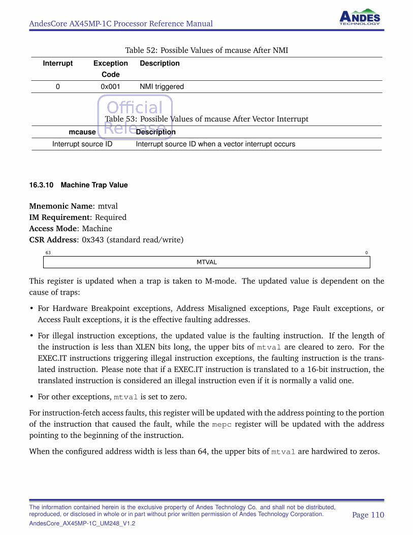
AndesCore AX45MP-1C Processor Reference Manual
Table 52: Possible Values of mcause After NMI
Interrupt ExceptionCode
Description
0 0x001 NMI triggered
Table 53: Possible Values of mcause After Vector Interrupt
mcause Description
Interrupt source ID Interrupt source ID when a vector interrupt occurs
16.3.10 Machine Trap Value
Mnemonic Name: mtvalIM Requirement: RequiredAccess Mode: MachineCSR Address: 0x343 (standard read/write)
63 0
MTVAL
This register is updated when a trap is taken to M-mode. The updated value is dependent on thecause of traps:
• For Hardware Breakpoint exceptions, Address Misaligned exceptions, Page Fault exceptions, orAccess Fault exceptions, it is the effective faulting addresses.
• For illegal instruction exceptions, the updated value is the faulting instruction. If the length ofthe instruction is less than XLEN bits long, the upper bits of mtval are cleared to zero. For theEXEC.IT instructions triggering illegal instruction exceptions, the faulting instruction is the trans-lated instruction. Please note that if a EXEC.IT instruction is translated to a 16-bit instruction, thetranslated instruction is considered an illegal instruction even if it is normally a valid one.
• For other exceptions, mtval is set to zero.
For instruction-fetch access faults, this register will be updated with the address pointing to the portionof the instruction that caused the fault, while the mepc register will be updated with the addresspointing to the beginning of the instruction.
When the configured address width is less than 64, the upper bits of mtval are hardwired to zeros.
The information contained herein is the exclusive property of Andes Technology Co. and shall not be distributed,reproduced, or disclosed in whole or in part without prior written permission of Andes Technology Corporation.AndesCore_AX45MP-1C_UM248_V1.2
Page 110
AndesCore AX45MP-1C Processor Reference Manual
Field Name Bits Description Type Reset
MTVAL [63:0] Exception-specific information for software traphandling.
RW 0
16.3.11 Machine Interrupt Pending
Mnemonic Name: mipIM Requirement: RequiredAccess Mode: MachineCSR Address: 0x344 (standard read/write)
63 19
0
18
PMOVI
17
BWEI
16
IMECCI
15 12
0
11
MEIP
10
0
9
SEIP
8
UEIP
7
MTIP
6
0
5
STIP
4
UTIP
3
MSIP
2
0
1
SSIP
0
USIP
Field Name Bits Description Type Reset
USIP [0] U-mode software interrupt pending bit.
Value Meaning
0 Not pending
1 Pending
RW 0
SSIP [1] S-mode software interrupt pending bit.
Value Meaning
0 Not pending
1 Pending
RW 0
MSIP [3] M-mode software interrupt pending bit.
Value Meaning
0 Not pending
1 Pending
RO 0
UTIP [4] U-mode timer interrupt pending bit.
Value Meaning
0 Not pending
1 Pending
RW 0
Continued on next page. . .
The information contained herein is the exclusive property of Andes Technology Co. and shall not be distributed,reproduced, or disclosed in whole or in part without prior written permission of Andes Technology Corporation.AndesCore_AX45MP-1C_UM248_V1.2
Page 111
AndesCore AX45MP-1C Processor Reference Manual
Field Name Bits Description Type Reset
STIP [5] S-mode timer interrupt pending bit.
Value Meaning
0 Not pending
1 Pending
RW 0
MTIP [7] M-mode timer interrupt pending bit.
Value Meaning
0 Not pending
1 Pending
RO 0
UEIP [8] U-mode external interrupt pending bit.
Value Meaning
0 Not pending
1 Pending
RW 0
SEIP [9] S-mode external interrupt pending bit.
Value Meaning
0 Not pending
1 Pending
RW 0
MEIP [11] M-mode external interrupt pending bit.
Value Meaning
0 Not pending
1 Pending
RO 0
IMECCI [16] Imprecise ECC error local interrupt pending bit.The processor may receive imprecise ECCerrors on slave port accesses or cachewritebacks.
Value Meaning
0 Not pending
1 Pending
RW 0
Continued on next page. . .
The information contained herein is the exclusive property of Andes Technology Co. and shall not be distributed,reproduced, or disclosed in whole or in part without prior written permission of Andes Technology Corporation.AndesCore_AX45MP-1C_UM248_V1.2
Page 112
AndesCore AX45MP-1C Processor Reference Manual
Field Name Bits Description Type Reset
BWEI [17] Bus read/write transaction error local interruptpending bit. The processor may receive buserrors on load/store instructions or cachewritebacks.
Value Meaning
0 Not pending
1 Pending
RW 0
PMOVI [18] Performance monitor overflow local interruptpending bit.
Value Meaning
0 Not pending
1 Pending
RW 0
When supervisor mode or N extension is not supported, the corresponding bits in mip are hardwiredto zero.
Each local interrupt can be configured with a local interrupt number. Bit location of interrupts are thesame as their interrupt numbers. Register fields above show the default bit location.
16.3.12 Machine Extended Status
Mnemonic Name: mxstatusIM Requirement: RequiredAccess Mode: MachineCSR Address: 0x7c4 (non-standard read/write)
63 10
0
9 6
0
5
PDME
4
DME
3 2
0
1
PPFT_EN
0
PFT_EN
The information contained herein is the exclusive property of Andes Technology Co. and shall not be distributed,reproduced, or disclosed in whole or in part without prior written permission of Andes Technology Corporation.AndesCore_AX45MP-1C_UM248_V1.2
Page 113
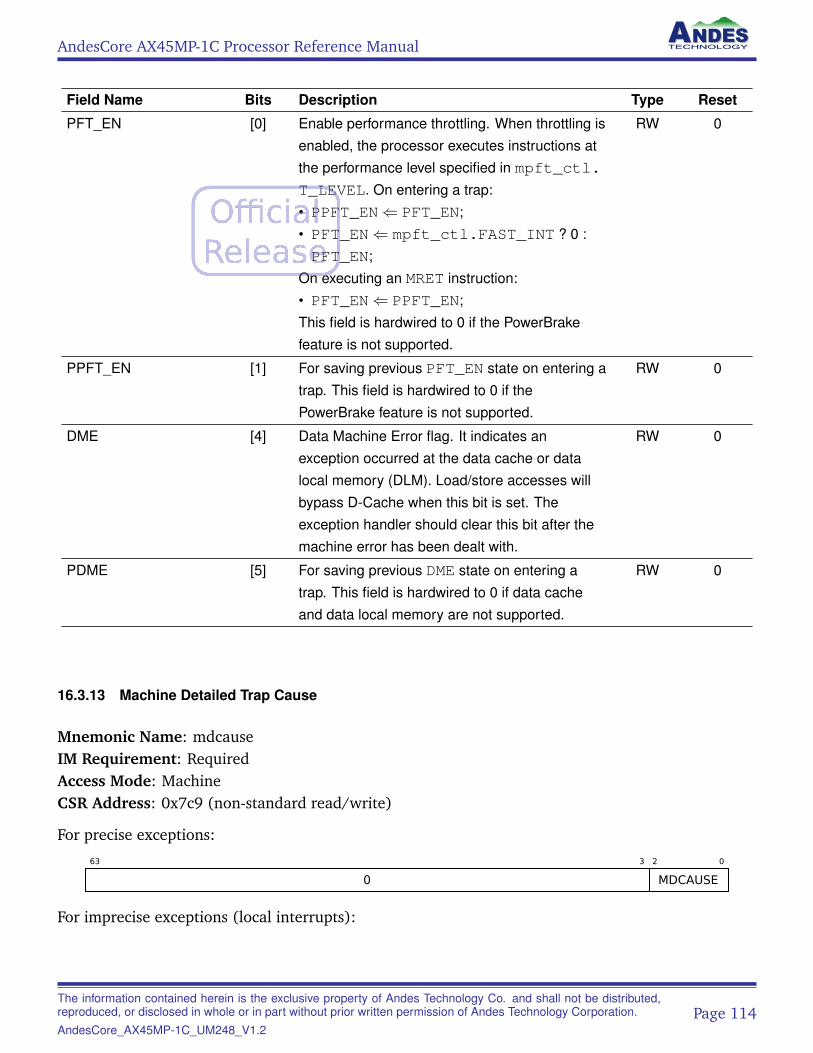
AndesCore AX45MP-1C Processor Reference Manual
Field Name Bits Description Type Reset
PFT_EN [0] Enable performance throttling. When throttling isenabled, the processor executes instructions atthe performance level specified in mpft_ctl.T_LEVEL. On entering a trap:• PPFT_EN⇐ PFT_EN;• PFT_EN⇐ mpft_ctl.FAST_INT ? 0 :PFT_EN;
On executing an MRET instruction:• PFT_EN⇐ PPFT_EN;This field is hardwired to 0 if the PowerBrakefeature is not supported.
RW 0
PPFT_EN [1] For saving previous PFT_EN state on entering atrap. This field is hardwired to 0 if thePowerBrake feature is not supported.
RW 0
DME [4] Data Machine Error flag. It indicates anexception occurred at the data cache or datalocal memory (DLM). Load/store accesses willbypass D-Cache when this bit is set. Theexception handler should clear this bit after themachine error has been dealt with.
RW 0
PDME [5] For saving previous DME state on entering atrap. This field is hardwired to 0 if data cacheand data local memory are not supported.
RW 0
16.3.13 Machine Detailed Trap Cause
Mnemonic Name: mdcauseIM Requirement: RequiredAccess Mode: MachineCSR Address: 0x7c9 (non-standard read/write)
For precise exceptions:
63 3
0
2 0
MDCAUSE
For imprecise exceptions (local interrupts):
The information contained herein is the exclusive property of Andes Technology Co. and shall not be distributed,reproduced, or disclosed in whole or in part without prior written permission of Andes Technology Corporation.AndesCore_AX45MP-1C_UM248_V1.2
Page 114
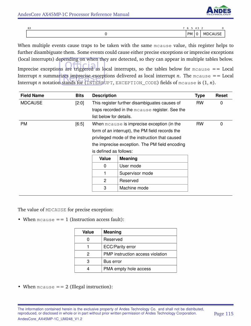
AndesCore AX45MP-1C Processor Reference Manual
63 7
0
6 5
PM
4 3
0
2 0
MDCAUSE
When multiple events cause traps to be taken with the same mcause value, this register helps tofurther disambiguate them. Some events could cause either precise exceptions or imprecise exceptions(local interrupts) depending on when they are detected, so they can appear in multiple tables below.
Imprecise exceptions are triggered as local interrupts, so the tables below for mcause == LocalInterrupt n summarizes imprecise exceptions delivered as local interrupt n. The mcause == LocalInterrupt n notation stands for (INTERRUPT, EXCEPTION_CODE) fields of mcause is (1, n).
Field Name Bits Description Type Reset
MDCAUSE [2:0] This register further disambiguates causes oftraps recorded in the mcause register. See thelist below for details.
RW 0
PM [6:5] When mcause is imprecise exception (in theform of an interrupt), the PM field records theprivileged mode of the instruction that causedthe imprecise exception. The PM field encodingis defined as follows:
Value Meaning
0 User mode
1 Supervisor mode
2 Reserved
3 Machine mode
RW 0
The value of MDCAUSE for precise exception:
• When mcause == 1 (Instruction access fault):
Value Meaning
0 Reserved
1 ECC/Parity error
2 PMP instruction access violation
3 Bus error
4 PMA empty hole access
• When mcause == 2 (Illegal instruction):
The information contained herein is the exclusive property of Andes Technology Co. and shall not be distributed,reproduced, or disclosed in whole or in part without prior written permission of Andes Technology Corporation.AndesCore_AX45MP-1C_UM248_V1.2
Page 115
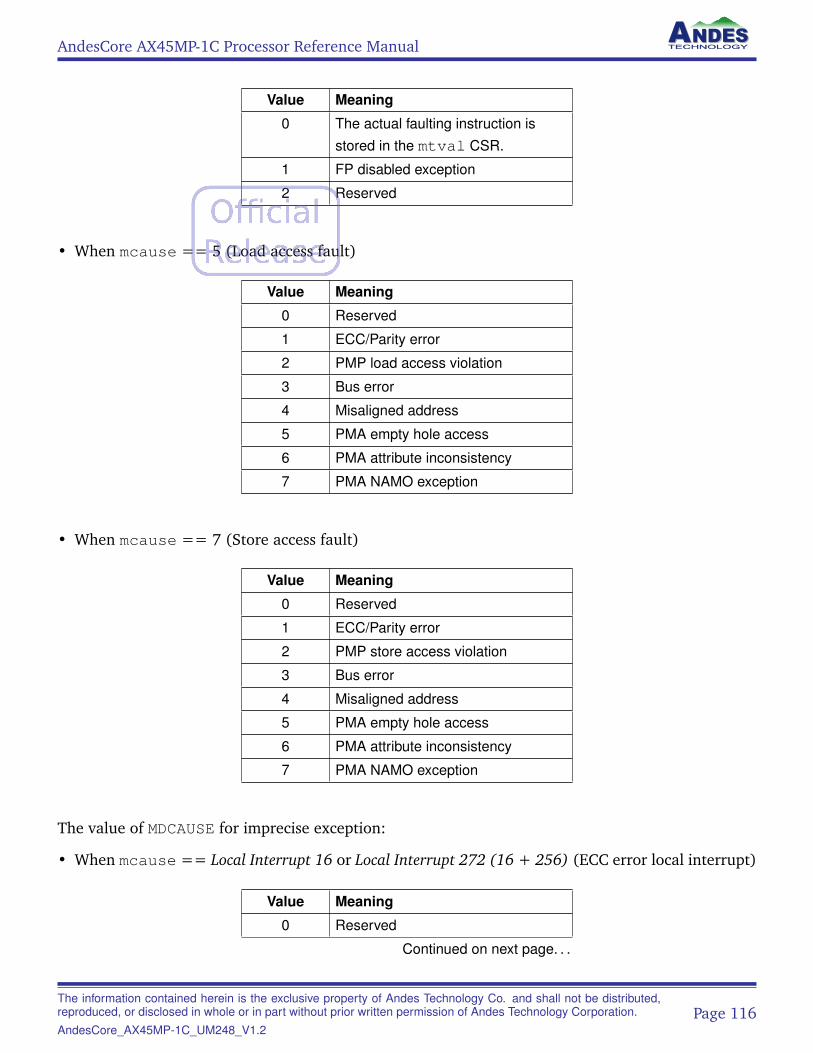
AndesCore AX45MP-1C Processor Reference Manual
Value Meaning
0 The actual faulting instruction isstored in the mtval CSR.
1 FP disabled exception
2 Reserved
• When mcause == 5 (Load access fault)
Value Meaning
0 Reserved
1 ECC/Parity error
2 PMP load access violation
3 Bus error
4 Misaligned address
5 PMA empty hole access
6 PMA attribute inconsistency
7 PMA NAMO exception
• When mcause == 7 (Store access fault)
Value Meaning
0 Reserved
1 ECC/Parity error
2 PMP store access violation
3 Bus error
4 Misaligned address
5 PMA empty hole access
6 PMA attribute inconsistency
7 PMA NAMO exception
The value of MDCAUSE for imprecise exception:
• When mcause == Local Interrupt 16 or Local Interrupt 272 (16 + 256) (ECC error local interrupt)
Value Meaning
0 Reserved
Continued on next page. . .
The information contained herein is the exclusive property of Andes Technology Co. and shall not be distributed,reproduced, or disclosed in whole or in part without prior written permission of Andes Technology Corporation.AndesCore_AX45MP-1C_UM248_V1.2
Page 116
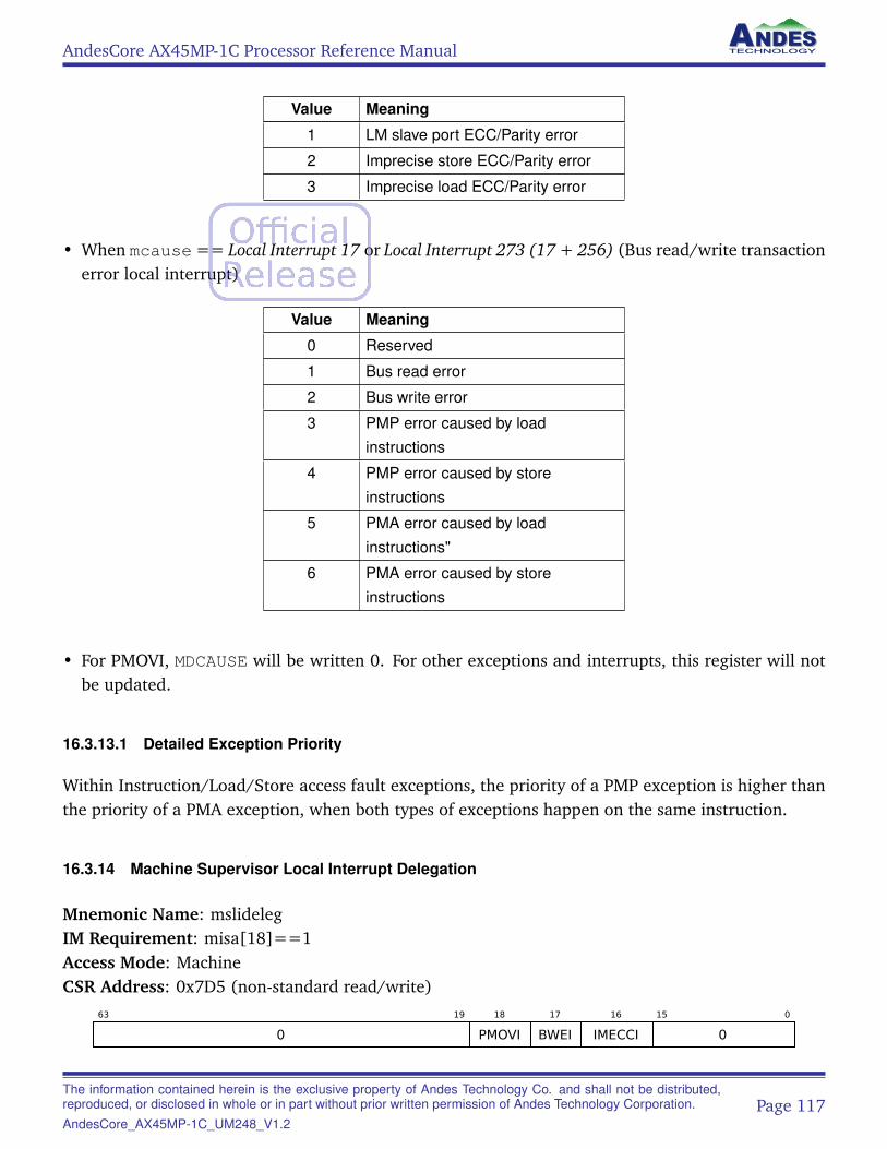
AndesCore AX45MP-1C Processor Reference Manual
Value Meaning
1 LM slave port ECC/Parity error
2 Imprecise store ECC/Parity error
3 Imprecise load ECC/Parity error
• When mcause == Local Interrupt 17 or Local Interrupt 273 (17 + 256) (Bus read/write transactionerror local interrupt)
Value Meaning
0 Reserved
1 Bus read error
2 Bus write error
3 PMP error caused by loadinstructions
4 PMP error caused by storeinstructions
5 PMA error caused by loadinstructions"
6 PMA error caused by storeinstructions
• For PMOVI, MDCAUSE will be written 0. For other exceptions and interrupts, this register will notbe updated.
16.3.13.1 Detailed Exception Priority
Within Instruction/Load/Store access fault exceptions, the priority of a PMP exception is higher thanthe priority of a PMA exception, when both types of exceptions happen on the same instruction.
16.3.14 Machine Supervisor Local Interrupt Delegation
Mnemonic Name: mslidelegIM Requirement: misa[18]==1Access Mode: MachineCSR Address: 0x7D5 (non-standard read/write)
63 19
0
18
PMOVI
17
BWEI
16
IMECCI
15 0
0
The information contained herein is the exclusive property of Andes Technology Co. and shall not be distributed,reproduced, or disclosed in whole or in part without prior written permission of Andes Technology Corporation.AndesCore_AX45MP-1C_UM248_V1.2
Page 117
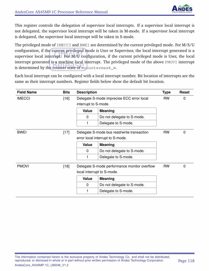
AndesCore AX45MP-1C Processor Reference Manual
This register controls the delegation of supervisor local interrupts. If a supervisor local interrupt isnot delegated, the supervisor local interrupt will be taken in M-mode. If a supervisor local interruptis delegated, the supervisor local interrupt will be taken in S-mode.
The privileged mode of IMECCI and BWEI are determined by the current privileged mode. For M/S/Uconfiguration, if the current privileged mode is User or Supervisor, the local interrupt generated is asupervisor local interrupt. For M/U configuration, if the current privileged mode is User, the localinterrupt generated is a machine local interrupt. The privileged mode of the above PMOVI interruptis determined by the counter state of mcountermask_m.
Each local interrupt can be configured with a local interrupt number. Bit location of interrupts are thesame as their interrupt numbers. Register fields below show the default bit location.
Field Name Bits Description Type Reset
IMECCI [16] Delegate S-mode imprecise ECC error localinterrupt to S-mode.
Value Meaning
0 Do not delegate to S-mode.
1 Delegate to S-mode.
RW 0
BWEI [17] Delegate S-mode bus read/write transactionerror local interrupt to S-mode.
Value Meaning
0 Do not delegate to S-mode.
1 Delegate to S-mode.
RW 0
PMOVI [18] Delegate S-mode performance monitor overflowlocal interrupt to S-mode.
Value Meaning
0 Do not delegate to S-mode.
1 Delegate to S-mode.
RW 0
The information contained herein is the exclusive property of Andes Technology Co. and shall not be distributed,reproduced, or disclosed in whole or in part without prior written permission of Andes Technology Corporation.AndesCore_AX45MP-1C_UM248_V1.2
Page 118
AndesCore AX45MP-1C Processor Reference Manual
16.4 Counter Related CSRs
16.4.1 Machine Cycle Counter
Mnemonic Name: mcycleIM Requirement: RequiredAccess Mode: MachineCSR Address: 0xb00 (standard read/write)
The mcycle CSR counts the number of cycles that the hart has executed since some arbitrary time inthe past. The mcycle register has 64-bit precision.
The information contained herein is the exclusive property of Andes Technology Co. and shall not be distributed,reproduced, or disclosed in whole or in part without prior written permission of Andes Technology Corporation.AndesCore_AX45MP-1C_UM248_V1.2
Page 119
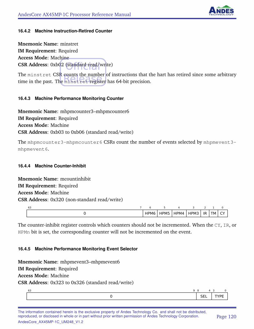
AndesCore AX45MP-1C Processor Reference Manual
16.4.2 Machine Instruction-Retired Counter
Mnemonic Name: minstretIM Requirement: RequiredAccess Mode: MachineCSR Address: 0xb02 (standard read/write)
The minstret CSR counts the number of instructions that the hart has retired since some arbitrarytime in the past. The minstret register has 64-bit precision.
16.4.3 Machine Performance Monitoring Counter
Mnemonic Name: mhpmcounter3–mhpmcounter6IM Requirement: RequiredAccess Mode: MachineCSR Address: 0xb03 to 0xb06 (standard read/write)
The mhpmcounter3-mhpmcounter6 CSRs count the number of events selected by mhpmevent3-mhpmevent6.
16.4.4 Machine Counter-Inhibit
Mnemonic Name: mcountinhibitIM Requirement: RequiredAccess Mode: MachineCSR Address: 0x320 (non-standard read/write)
63 7
0
6
HPM6
5
HPM5
4
HPM4
3
HPM3
2
IR
1
TM
0
CY
The counter-inhibit register controls which counters should not be incremented. When the CY, IR, orHPMn bit is set, the corresponding counter will not be incremented on the event.
16.4.5 Machine Performance Monitoring Event Selector
Mnemonic Name: mhpmevent3–mhpmevent6IM Requirement: RequiredAccess Mode: MachineCSR Address: 0x323 to 0x326 (standard read/write)
63 9
0
8 4
SEL
3 0
TYPE
The information contained herein is the exclusive property of Andes Technology Co. and shall not be distributed,reproduced, or disclosed in whole or in part without prior written permission of Andes Technology Corporation.AndesCore_AX45MP-1C_UM248_V1.2
Page 120
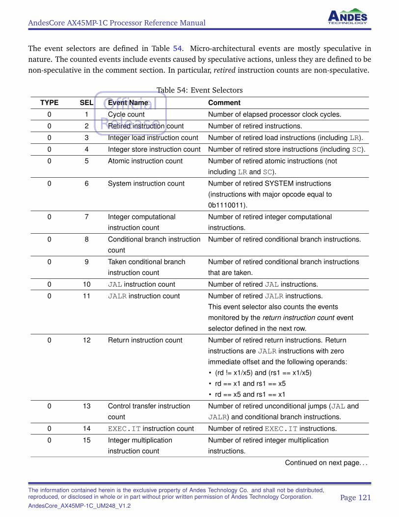
AndesCore AX45MP-1C Processor Reference Manual
The event selectors are defined in Table 54. Micro-architectural events are mostly speculative innature. The counted events include events caused by speculative actions, unless they are defined to benon-speculative in the comment section. In particular, retired instruction counts are non-speculative.
Table 54: Event Selectors
TYPE SEL Event Name Comment
0 1 Cycle count Number of elapsed processor clock cycles.
0 2 Retired instruction count Number of retired instructions.
0 3 Integer load instruction count Number of retired load instructions (including LR).
0 4 Integer store instruction count Number of retired store instructions (including SC).
0 5 Atomic instruction count Number of retired atomic instructions (notincluding LR and SC).
0 6 System instruction count Number of retired SYSTEM instructions(instructions with major opcode equal to0b1110011).
0 7 Integer computationalinstruction count
Number of retired integer computationalinstructions.
0 8 Conditional branch instructioncount
Number of retired conditional branch instructions.
0 9 Taken conditional branchinstruction count
Number of retired conditional branch instructionsthat are taken.
0 10 JAL instruction count Number of retired JAL instructions.
0 11 JALR instruction count Number of retired JALR instructions.This event selector also counts the eventsmonitored by the return instruction count eventselector defined in the next row.
0 12 Return instruction count Number of retired return instructions. Returninstructions are JALR instructions with zeroimmediate offset and the following operands:• (rd != x1/x5) and (rs1 == x1/x5)• rd == x1 and rs1 == x5• rd == x5 and rs1 == x1
0 13 Control transfer instructioncount
Number of retired unconditional jumps (JAL andJALR) and conditional branch instructions.
0 14 EXEC.IT instruction count Number of retired EXEC.IT instructions.
0 15 Integer multiplicationinstruction count
Number of retired integer multiplicationinstructions.
Continued on next page. . .
The information contained herein is the exclusive property of Andes Technology Co. and shall not be distributed,reproduced, or disclosed in whole or in part without prior written permission of Andes Technology Corporation.AndesCore_AX45MP-1C_UM248_V1.2
Page 121
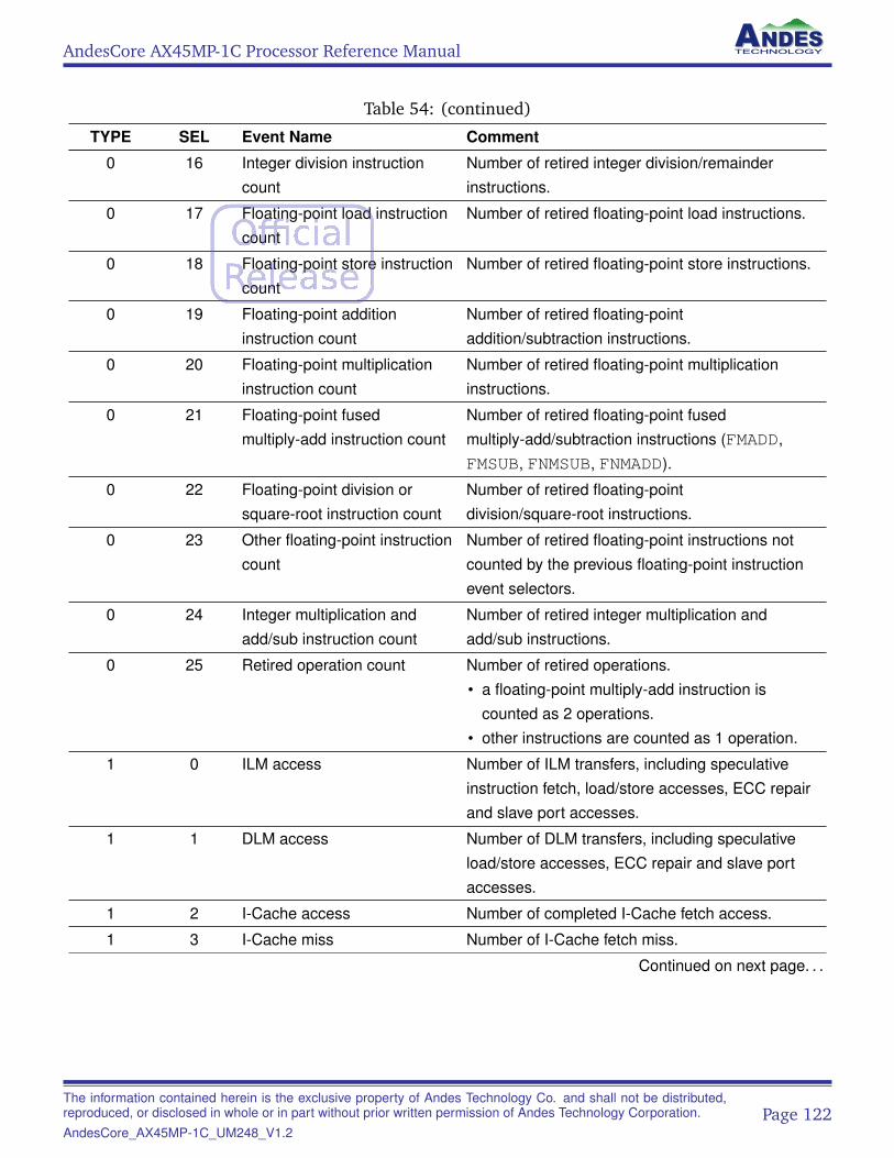
AndesCore AX45MP-1C Processor Reference Manual
Table 54: (continued)
TYPE SEL Event Name Comment
0 16 Integer division instructioncount
Number of retired integer division/remainderinstructions.
0 17 Floating-point load instructioncount
Number of retired floating-point load instructions.
0 18 Floating-point store instructioncount
Number of retired floating-point store instructions.
0 19 Floating-point additioninstruction count
Number of retired floating-pointaddition/subtraction instructions.
0 20 Floating-point multiplicationinstruction count
Number of retired floating-point multiplicationinstructions.
0 21 Floating-point fusedmultiply-add instruction count
Number of retired floating-point fusedmultiply-add/subtraction instructions (FMADD,FMSUB, FNMSUB, FNMADD).
0 22 Floating-point division orsquare-root instruction count
Number of retired floating-pointdivision/square-root instructions.
0 23 Other floating-point instructioncount
Number of retired floating-point instructions notcounted by the previous floating-point instructionevent selectors.
0 24 Integer multiplication andadd/sub instruction count
Number of retired integer multiplication andadd/sub instructions.
0 25 Retired operation count Number of retired operations.• a floating-point multiply-add instruction is
counted as 2 operations.• other instructions are counted as 1 operation.
1 0 ILM access Number of ILM transfers, including speculativeinstruction fetch, load/store accesses, ECC repairand slave port accesses.
1 1 DLM access Number of DLM transfers, including speculativeload/store accesses, ECC repair and slave portaccesses.
1 2 I-Cache access Number of completed I-Cache fetch access.
1 3 I-Cache miss Number of I-Cache fetch miss.
Continued on next page. . .
The information contained herein is the exclusive property of Andes Technology Co. and shall not be distributed,reproduced, or disclosed in whole or in part without prior written permission of Andes Technology Corporation.AndesCore_AX45MP-1C_UM248_V1.2
Page 122
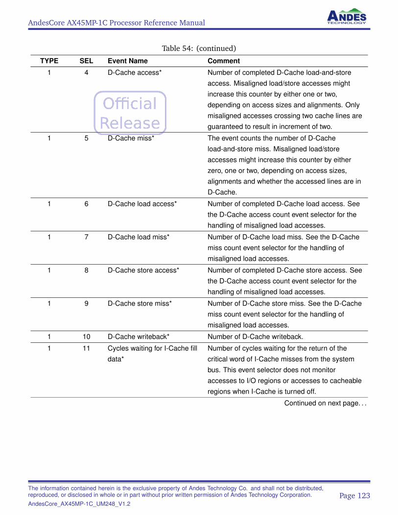
AndesCore AX45MP-1C Processor Reference Manual
Table 54: (continued)
TYPE SEL Event Name Comment
1 4 D-Cache access* Number of completed D-Cache load-and-storeaccess. Misaligned load/store accesses mightincrease this counter by either one or two,depending on access sizes and alignments. Onlymisaligned accesses crossing two cache lines areguaranteed to result in increment of two.
1 5 D-Cache miss* The event counts the number of D-Cacheload-and-store miss. Misaligned load/storeaccesses might increase this counter by eitherzero, one or two, depending on access sizes,alignments and whether the accessed lines are inD-Cache.
1 6 D-Cache load access* Number of completed D-Cache load access. Seethe D-Cache access count event selector for thehandling of misaligned load accesses.
1 7 D-Cache load miss* Number of D-Cache load miss. See the D-Cachemiss count event selector for the handling ofmisaligned load accesses.
1 8 D-Cache store access* Number of completed D-Cache store access. Seethe D-Cache access count event selector for thehandling of misaligned load accesses.
1 9 D-Cache store miss* Number of D-Cache store miss. See the D-Cachemiss count event selector for the handling ofmisaligned load accesses.
1 10 D-Cache writeback* Number of D-Cache writeback.
1 11 Cycles waiting for I-Cache filldata*
Number of cycles waiting for the return of thecritical word of I-Cache misses from the systembus. This event selector does not monitoraccesses to I/O regions or accesses to cacheableregions when I-Cache is turned off.
Continued on next page. . .
The information contained herein is the exclusive property of Andes Technology Co. and shall not be distributed,reproduced, or disclosed in whole or in part without prior written permission of Andes Technology Corporation.AndesCore_AX45MP-1C_UM248_V1.2
Page 123
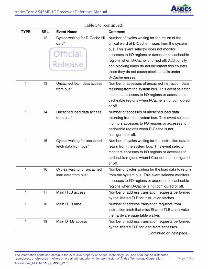
AndesCore AX45MP-1C Processor Reference Manual
Table 54: (continued)
TYPE SEL Event Name Comment
1 12 Cycles waiting for D-Cache filldata*
Number of cycles waiting for the return of thecritical word of D-Cache misses from the systembus. This event selector does not monitoraccesses to I/O regions or accesses to cacheableregions when D-Cache is turned off. Additionally,non-blocking loads do not increment this countersince they do not cause pipeline stalls underD-Cache misses.
1 13 Uncached fetch data accessfrom bus*
Number of accesses of uncached instruction datareturning from the system bus. This event selectormonitors accesses to I/O regions or accesses tocacheable regions when I-Cache is not configuredor off.
1 14 Uncached load data accessfrom bus*
Number of accesses of uncached load datareturning from the system bus. This event selectormonitors accesses to I/O regions or accesses tocacheable regions when D-Cache is notconfigured or off.
1 15 Cycles waiting for uncachedfetch data from bus*
Number of cycles waiting for the instruction data toreturn from the system bus. This event selectormonitors accesses to I/O regions or accesses tocacheable regions when I-Cache is not configuredor off.
1 16 Cycles waiting for uncachedload data from bus*
Number of cycles waiting for the load data to returnfrom the system bus. This event selector monitorsaccesses to I/O regions or accesses to cacheableregions when D-Cache is not configured or off.
1 17 Main ITLB access Number of address translation requests performedby the shared TLB for instruction fetches
1 18 Main ITLB miss Number of address translation requests frominstruction fetch that miss Shared TLB and invokethe hardware page table walker.
1 19 Main DTLB access Number of address translation requests performedby the shared TLB for load/store accesses
Continued on next page. . .
The information contained herein is the exclusive property of Andes Technology Co. and shall not be distributed,reproduced, or disclosed in whole or in part without prior written permission of Andes Technology Corporation.AndesCore_AX45MP-1C_UM248_V1.2
Page 124
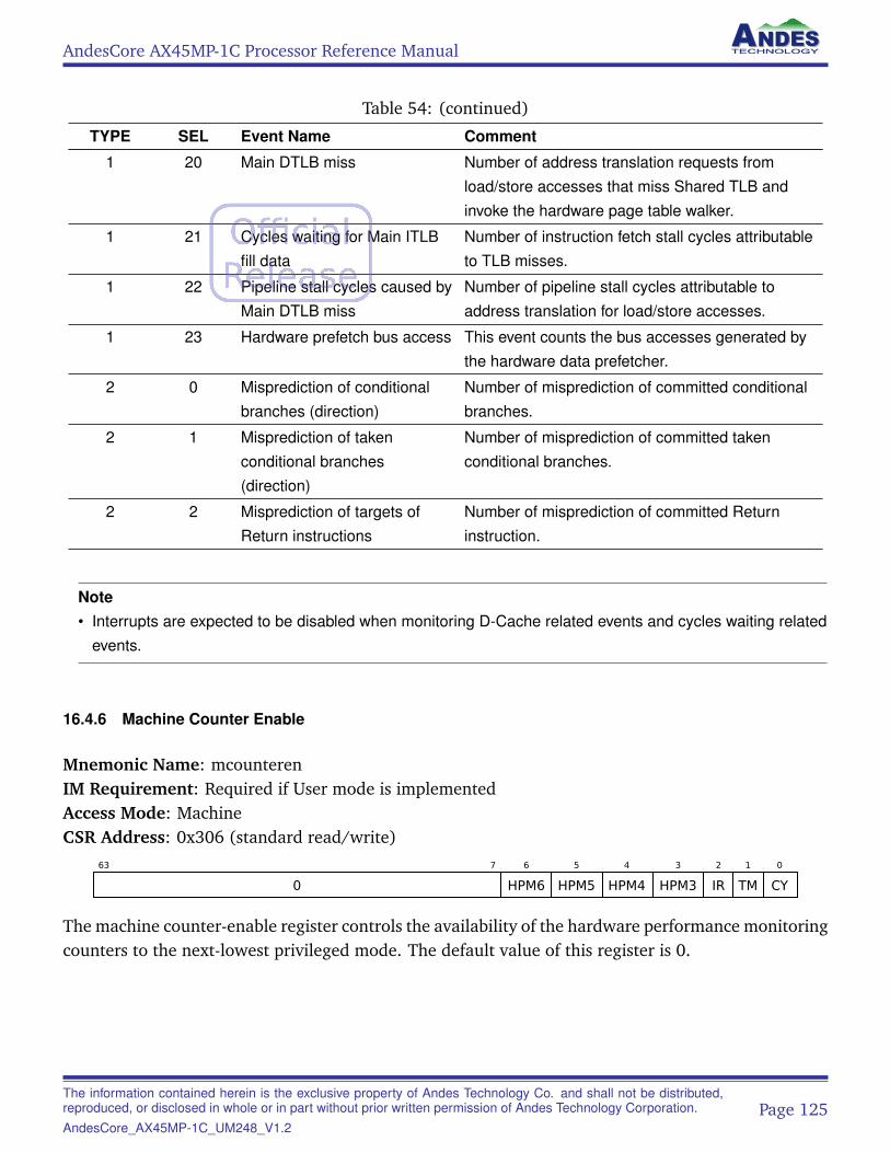
AndesCore AX45MP-1C Processor Reference Manual
Table 54: (continued)
TYPE SEL Event Name Comment
1 20 Main DTLB miss Number of address translation requests fromload/store accesses that miss Shared TLB andinvoke the hardware page table walker.
1 21 Cycles waiting for Main ITLBfill data
Number of instruction fetch stall cycles attributableto TLB misses.
1 22 Pipeline stall cycles caused byMain DTLB miss
Number of pipeline stall cycles attributable toaddress translation for load/store accesses.
1 23 Hardware prefetch bus access This event counts the bus accesses generated bythe hardware data prefetcher.
2 0 Misprediction of conditionalbranches (direction)
Number of misprediction of committed conditionalbranches.
2 1 Misprediction of takenconditional branches(direction)
Number of misprediction of committed takenconditional branches.
2 2 Misprediction of targets ofReturn instructions
Number of misprediction of committed Returninstruction.
Note• Interrupts are expected to be disabled when monitoring D-Cache related events and cycles waiting related
events.
16.4.6 Machine Counter Enable
Mnemonic Name: mcounterenIM Requirement: Required if User mode is implementedAccess Mode: MachineCSR Address: 0x306 (standard read/write)
63 7
0
6
HPM6
5
HPM5
4
HPM4
3
HPM3
2
IR
1
TM
0
CY
The machine counter-enable register controls the availability of the hardware performance monitoringcounters to the next-lowest privileged mode. The default value of this register is 0.
The information contained herein is the exclusive property of Andes Technology Co. and shall not be distributed,reproduced, or disclosed in whole or in part without prior written permission of Andes Technology Corporation.AndesCore_AX45MP-1C_UM248_V1.2
Page 125
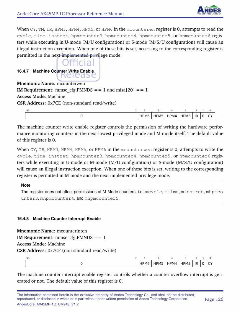
AndesCore AX45MP-1C Processor Reference Manual
When CY, TM, IR, HPM3, HPM4, HPM5, or HPM6 in the mcounteren register is 0, attempts to read thecycle, time, instret, hpmcounter3, hpmcounter4, hpmcounter5, or hpmcounter6 regis-ters while executing in U-mode (M/U configuration) or S-mode (M/S/U configuration) will cause anillegal instruction exception. When one of these bits is set, accessing to the corresponding register ispermitted in the next implemented privilege mode.
16.4.7 Machine Counter Write Enable
Mnemonic Name: mcounterwenIM Requirement: mmsc_cfg.PMNDS == 1 and misa[20] == 1Access Mode: MachineCSR Address: 0x7CE (non-standard read/write)
63 7
0
6
HPM6
5
HPM5
4
HPM4
3
HPM3
2
IR
1
0
0
CY
The machine counter write enable register controls the permission of writing the hardware perfor-mance monitoring counters in the next-lowest privileged mode and M-mode itself. The default valueof this register is 0.
When CY, IR, HPM3, HPM4, HPM5, or HPM6 in the mcounterwen register is 0, attempts to write thecycle, time, instret, hpmcounter3, hpmcounter4, hpmcounter5, or hpmcounter6 regis-ters while executing in U-mode or M-mode (M/U configuration) or S-mode (M/S/U configuration)will cause an illegal instruction exception. When one of these bits is set, writing to the correspondingregister is permitted in M-mode and the next implemented privilege mode.
NoteThe register does not affect permissions of M-Mode counters, i.e. mcycle, mtime, minstret, mhpmcounter3, mhpmcounter4, and mhpmcounter5.
16.4.8 Machine Counter Interrupt Enable
Mnemonic Name: mcounterintenIM Requirement: mmsc_cfg.PMNDS == 1Access Mode: MachineCSR Address: 0x7CF (non-standard read/write)
63 7
0
6
HPM6
5
HPM5
4
HPM4
3
HPM3
2
IR
1
0
0
CY
The machine counter interrupt enable register controls whether a counter overflow interrupt is gen-erated or not. The default value of this register is 0.
The information contained herein is the exclusive property of Andes Technology Co. and shall not be distributed,reproduced, or disclosed in whole or in part without prior written permission of Andes Technology Corporation.AndesCore_AX45MP-1C_UM248_V1.2
Page 126
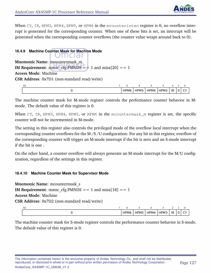
AndesCore AX45MP-1C Processor Reference Manual
When CY, IR, HPM3, HPM4, HPM5, or HPM6 in the mcounterinten register is 0, no overflow inter-rupt is generated for the corresponding counter. When one of these bits is set, an interrupt will begenerated when the corresponding counter overflows (the counter value wraps around back to 0).
16.4.9 Machine Counter Mask for Machine Mode
Mnemonic Name: mcountermask_mIM Requirement: mmsc_cfg.PMNDS == 1 and misa[20] == 1Access Mode: MachineCSR Address: 0x7D1 (non-standard read/write)
63 7
0
6
HPM6
5
HPM5
4
HPM4
3
HPM3
2
IR
1
0
0
CY
The machine counter mask for M-mode register controls the performance counter behavior in M-mode. The default value of this register is 0.
When CY, IR, HPM3, HPM4, HPM5, or HPM6 in the mcountermask_m register is set, the specificcounter will not be incremented in M-mode.
The setting in this register also controls the privileged mode of the overflow local interrupt when thecorresponding counter overflows for the M /S /U configuration: For any bit in this register, overflow ofthe corresponding counter will trigger an M-mode interrupt if the bit is zero and an S-mode interruptif the bit is one .
On the other hand, a counter overflow will always generate an M-mode interrupt for the M/U config-uration, regardless of the settings in this register.
16.4.10 Machine Counter Mask for Supervisor Mode
Mnemonic Name: mcountermask_sIM Requirement: mmsc_cfg.PMNDS == 1 and misa[18] == 1Access Mode: MachineCSR Address: 0x7D2 (non-standard read/write)
63 7
0
6
HPM6
5
HPM5
4
HPM4
3
HPM3
2
IR
1
0
0
CY
The machine counter mask for S-mode register controls the performance counter behavior in S-mode.The default value of this register is 0.
The information contained herein is the exclusive property of Andes Technology Co. and shall not be distributed,reproduced, or disclosed in whole or in part without prior written permission of Andes Technology Corporation.AndesCore_AX45MP-1C_UM248_V1.2
Page 127
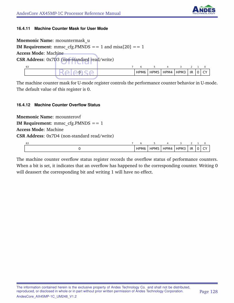
AndesCore AX45MP-1C Processor Reference Manual
16.4.11 Machine Counter Mask for User Mode
Mnemonic Name: mcountermask_uIM Requirement: mmsc_cfg.PMNDS == 1 and misa[20] == 1Access Mode: MachineCSR Address: 0x7D3 (non-standard read/write)
63 7
0
6
HPM6
5
HPM5
4
HPM4
3
HPM3
2
IR
1
0
0
CY
The machine counter mask for U-mode register controls the performance counter behavior in U-mode.The default value of this register is 0.
16.4.12 Machine Counter Overflow Status
Mnemonic Name: mcounterovfIM Requirement: mmsc_cfg.PMNDS == 1Access Mode: MachineCSR Address: 0x7D4 (non-standard read/write)
63 7
0
6
HPM6
5
HPM5
4
HPM4
3
HPM3
2
IR
1
0
0
CY
The machine counter overflow status register records the overflow status of performance counters.When a bit is set, it indicates that an overflow has happened to the corresponding counter. Writing 0will deassert the corresponding bit and writing 1 will have no effect.
The information contained herein is the exclusive property of Andes Technology Co. and shall not be distributed,reproduced, or disclosed in whole or in part without prior written permission of Andes Technology Corporation.AndesCore_AX45MP-1C_UM248_V1.2
Page 128
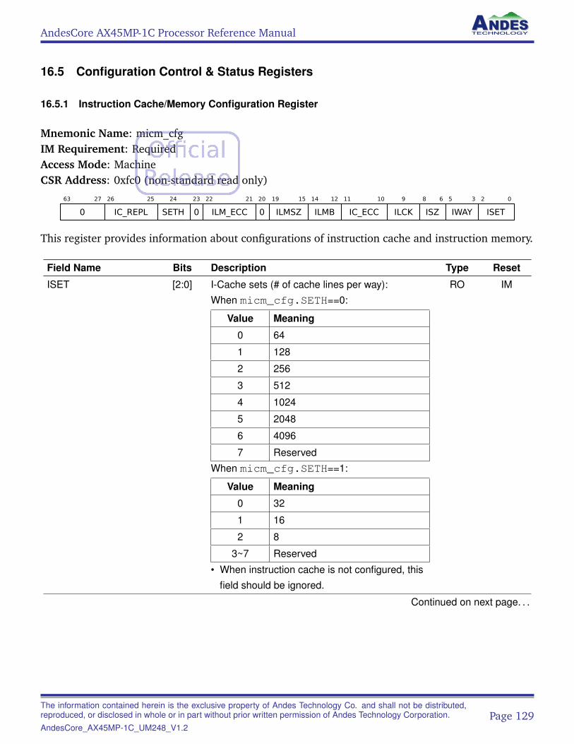
AndesCore AX45MP-1C Processor Reference Manual
16.5 Configuration Control & Status Registers
16.5.1 Instruction Cache/Memory Configuration Register
Mnemonic Name: micm_cfgIM Requirement: RequiredAccess Mode: MachineCSR Address: 0xfc0 (non-standard read only)
63 27
0
26 25
IC_REPL
24
SETH
23
0
22 21
ILM_ECC
20
0
19 15
ILMSZ
14 12
ILMB
11 10
IC_ECC
9
ILCK
8 6
ISZ
5 3
IWAY
2 0
ISET
This register provides information about configurations of instruction cache and instruction memory.
Field Name Bits Description Type Reset
ISET [2:0] I-Cache sets (# of cache lines per way):When micm_cfg.SETH==0:
Value Meaning
0 64
1 128
2 256
3 512
4 1024
5 2048
6 4096
7 Reserved
When micm_cfg.SETH==1:
Value Meaning
0 32
1 16
2 8
3~7 Reserved
• When instruction cache is not configured, thisfield should be ignored.
RO IM
Continued on next page. . .
The information contained herein is the exclusive property of Andes Technology Co. and shall not be distributed,reproduced, or disclosed in whole or in part without prior written permission of Andes Technology Corporation.AndesCore_AX45MP-1C_UM248_V1.2
Page 129
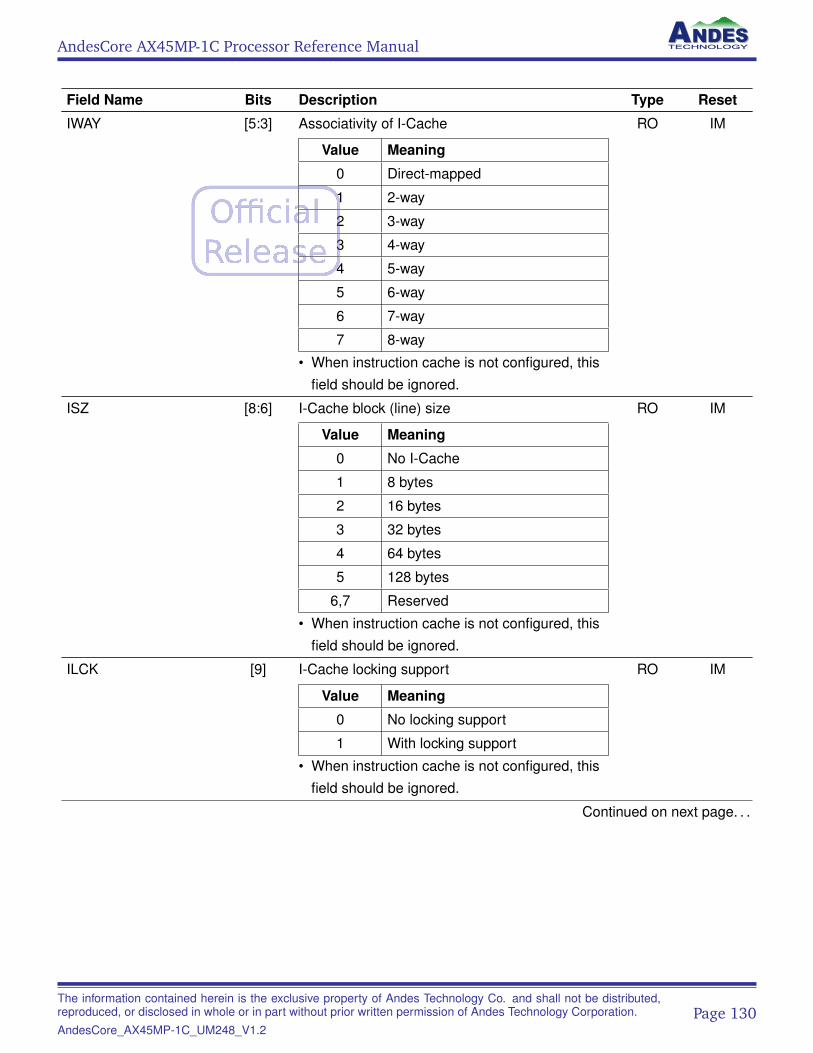
AndesCore AX45MP-1C Processor Reference Manual
Field Name Bits Description Type Reset
IWAY [5:3] Associativity of I-Cache
Value Meaning
0 Direct-mapped
1 2-way
2 3-way
3 4-way
4 5-way
5 6-way
6 7-way
7 8-way
• When instruction cache is not configured, thisfield should be ignored.
RO IM
ISZ [8:6] I-Cache block (line) size
Value Meaning
0 No I-Cache
1 8 bytes
2 16 bytes
3 32 bytes
4 64 bytes
5 128 bytes
6,7 Reserved
• When instruction cache is not configured, thisfield should be ignored.
RO IM
ILCK [9] I-Cache locking support
Value Meaning
0 No locking support
1 With locking support
• When instruction cache is not configured, thisfield should be ignored.
RO IM
Continued on next page. . .
The information contained herein is the exclusive property of Andes Technology Co. and shall not be distributed,reproduced, or disclosed in whole or in part without prior written permission of Andes Technology Corporation.AndesCore_AX45MP-1C_UM248_V1.2
Page 130
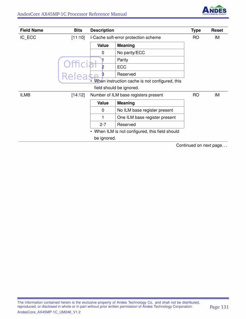
AndesCore AX45MP-1C Processor Reference Manual
Field Name Bits Description Type Reset
IC_ECC [11:10] I-Cache soft-error protection scheme
Value Meaning
0 No parity/ECC
1 Parity
2 ECC
3 Reserved
• When instruction cache is not configured, thisfield should be ignored.
RO IM
ILMB [14:12] Number of ILM base registers present
Value Meaning
0 No ILM base register present
1 One ILM base register present
2-7 Reserved
• When ILM is not configured, this field shouldbe ignored.
RO IM
Continued on next page. . .
The information contained herein is the exclusive property of Andes Technology Co. and shall not be distributed,reproduced, or disclosed in whole or in part without prior written permission of Andes Technology Corporation.AndesCore_AX45MP-1C_UM248_V1.2
Page 131

AndesCore AX45MP-1C Processor Reference Manual
Field Name Bits Description Type Reset
ILMSZ [19:15] ILM Size
Value Meaning
0 0 Byte
1 1 KiB
2 2 KiB
3 4 KiB
4 8 KiB
5 16 KiB
6 32 KiB
7 64 KiB
8 128 KiB
9 256 KiB
10 512 KiB
11 1 MiB
12 2 MiB
13 4 MiB
14 8 MiB
15 16 MiB
16-31 Reserved
• When ILM is not configured, this field shouldbe ignored.
RO IM
ILM_ECC [22:21] ILM soft-error protection scheme
Value Meaning
0 No parity/ECC
1 Parity
2 ECC
3 Reserved
• When ILM is not configured, this field shouldbe ignored.
RO IM
SETH [24] This bit extends the ISET field.• When instruction cache is not configured, this
field should be ignored.
RO IM
IC_REPL [26:25] This field is hardwired to zeros. RO 0
The information contained herein is the exclusive property of Andes Technology Co. and shall not be distributed,reproduced, or disclosed in whole or in part without prior written permission of Andes Technology Corporation.AndesCore_AX45MP-1C_UM248_V1.2
Page 132
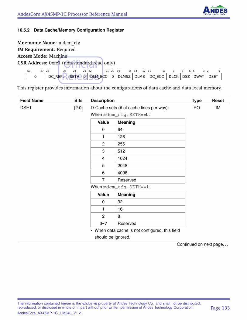
AndesCore AX45MP-1C Processor Reference Manual
16.5.2 Data Cache/Memory Configuration Register
Mnemonic Name: mdcm_cfgIM Requirement: RequiredAccess Mode: MachineCSR Address: 0xfc1 (non-standard read only)
63 27
0
26 25
DC_REPL
24
SETH
23
0
22 21
DLM_ECC
20
0
19 15
DLMSZ
14 12
DLMB
11 10
DC_ECC
9
DLCK
8 6
DSZ
5 3
DWAY
2 0
DSET
This register provides information about the configurations of data cache and data local memory.
Field Name Bits Description Type Reset
DSET [2:0] D-Cache sets (# of cache lines per way):When mdcm_cfg.SETH==0:
Value Meaning
0 64
1 128
2 256
3 512
4 1024
5 2048
6 4096
7 Reserved
When mdcm_cfg.SETH==1:
Value Meaning
0 32
1 16
2 8
3~7 Reserved
• When data cache is not configured, this fieldshould be ignored.
RO IM
Continued on next page. . .
The information contained herein is the exclusive property of Andes Technology Co. and shall not be distributed,reproduced, or disclosed in whole or in part without prior written permission of Andes Technology Corporation.AndesCore_AX45MP-1C_UM248_V1.2
Page 133
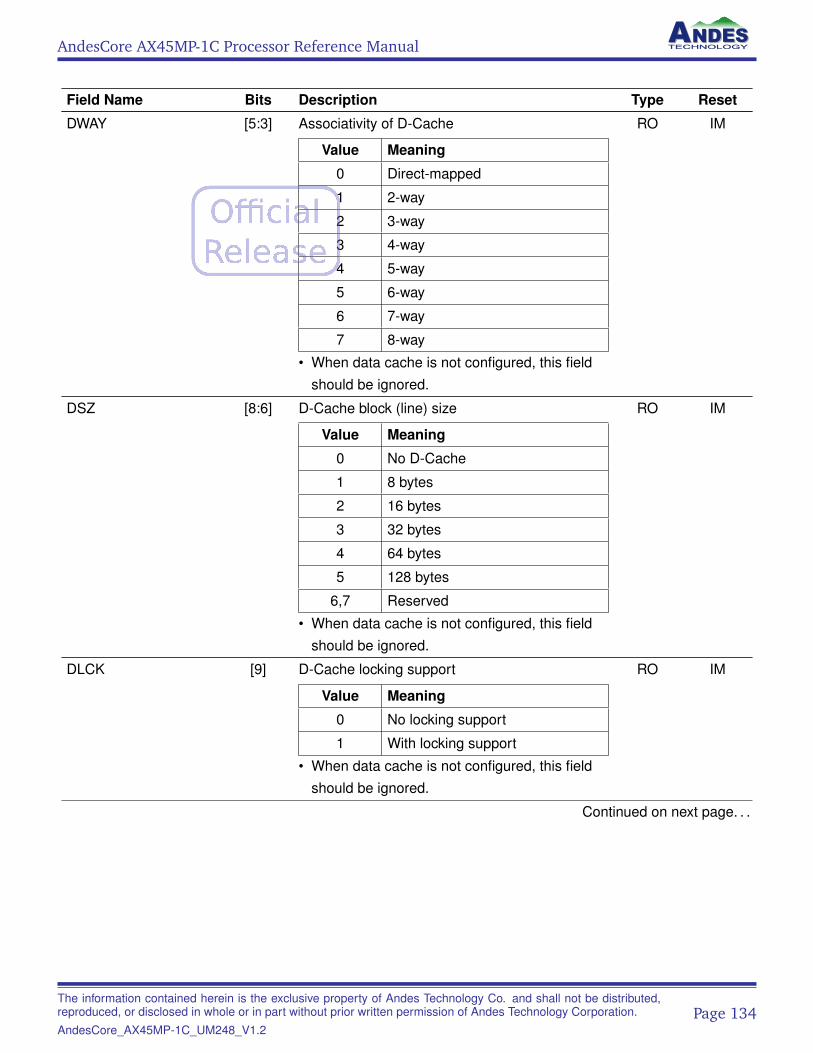
AndesCore AX45MP-1C Processor Reference Manual
Field Name Bits Description Type Reset
DWAY [5:3] Associativity of D-Cache
Value Meaning
0 Direct-mapped
1 2-way
2 3-way
3 4-way
4 5-way
5 6-way
6 7-way
7 8-way
• When data cache is not configured, this fieldshould be ignored.
RO IM
DSZ [8:6] D-Cache block (line) size
Value Meaning
0 No D-Cache
1 8 bytes
2 16 bytes
3 32 bytes
4 64 bytes
5 128 bytes
6,7 Reserved
• When data cache is not configured, this fieldshould be ignored.
RO IM
DLCK [9] D-Cache locking support
Value Meaning
0 No locking support
1 With locking support
• When data cache is not configured, this fieldshould be ignored.
RO IM
Continued on next page. . .
The information contained herein is the exclusive property of Andes Technology Co. and shall not be distributed,reproduced, or disclosed in whole or in part without prior written permission of Andes Technology Corporation.AndesCore_AX45MP-1C_UM248_V1.2
Page 134
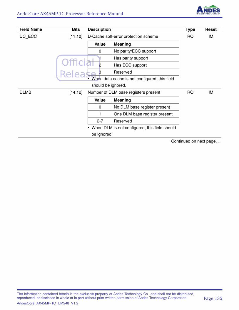
AndesCore AX45MP-1C Processor Reference Manual
Field Name Bits Description Type Reset
DC_ECC [11:10] D-Cache soft-error protection scheme
Value Meaning
0 No parity/ECC support
1 Has parity support
2 Has ECC support
3 Reserved
• When data cache is not configured, this fieldshould be ignored.
RO IM
DLMB [14:12] Number of DLM base registers present
Value Meaning
0 No DLM base register present
1 One DLM base register present
2-7 Reserved
• When DLM is not configured, this field shouldbe ignored.
RO IM
Continued on next page. . .
The information contained herein is the exclusive property of Andes Technology Co. and shall not be distributed,reproduced, or disclosed in whole or in part without prior written permission of Andes Technology Corporation.AndesCore_AX45MP-1C_UM248_V1.2
Page 135
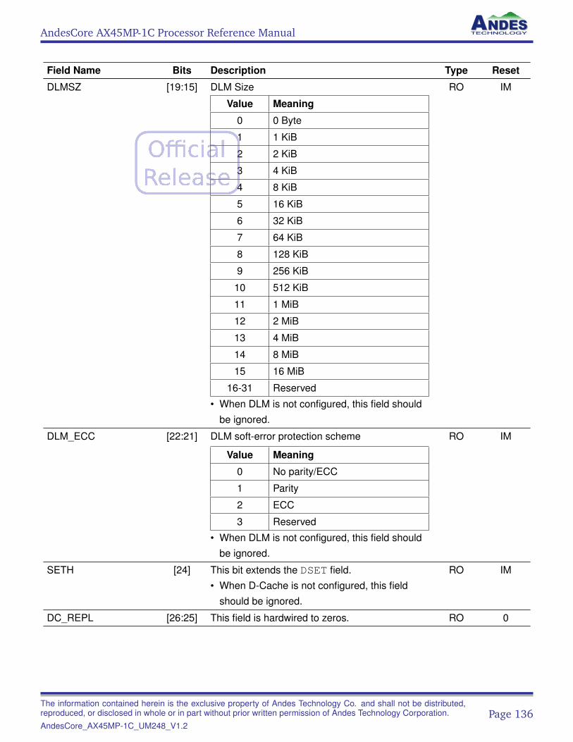
AndesCore AX45MP-1C Processor Reference Manual
Field Name Bits Description Type Reset
DLMSZ [19:15] DLM Size
Value Meaning
0 0 Byte
1 1 KiB
2 2 KiB
3 4 KiB
4 8 KiB
5 16 KiB
6 32 KiB
7 64 KiB
8 128 KiB
9 256 KiB
10 512 KiB
11 1 MiB
12 2 MiB
13 4 MiB
14 8 MiB
15 16 MiB
16-31 Reserved
• When DLM is not configured, this field shouldbe ignored.
RO IM
DLM_ECC [22:21] DLM soft-error protection scheme
Value Meaning
0 No parity/ECC
1 Parity
2 ECC
3 Reserved
• When DLM is not configured, this field shouldbe ignored.
RO IM
SETH [24] This bit extends the DSET field.• When D-Cache is not configured, this field
should be ignored.
RO IM
DC_REPL [26:25] This field is hardwired to zeros. RO 0
The information contained herein is the exclusive property of Andes Technology Co. and shall not be distributed,reproduced, or disclosed in whole or in part without prior written permission of Andes Technology Corporation.AndesCore_AX45MP-1C_UM248_V1.2
Page 136
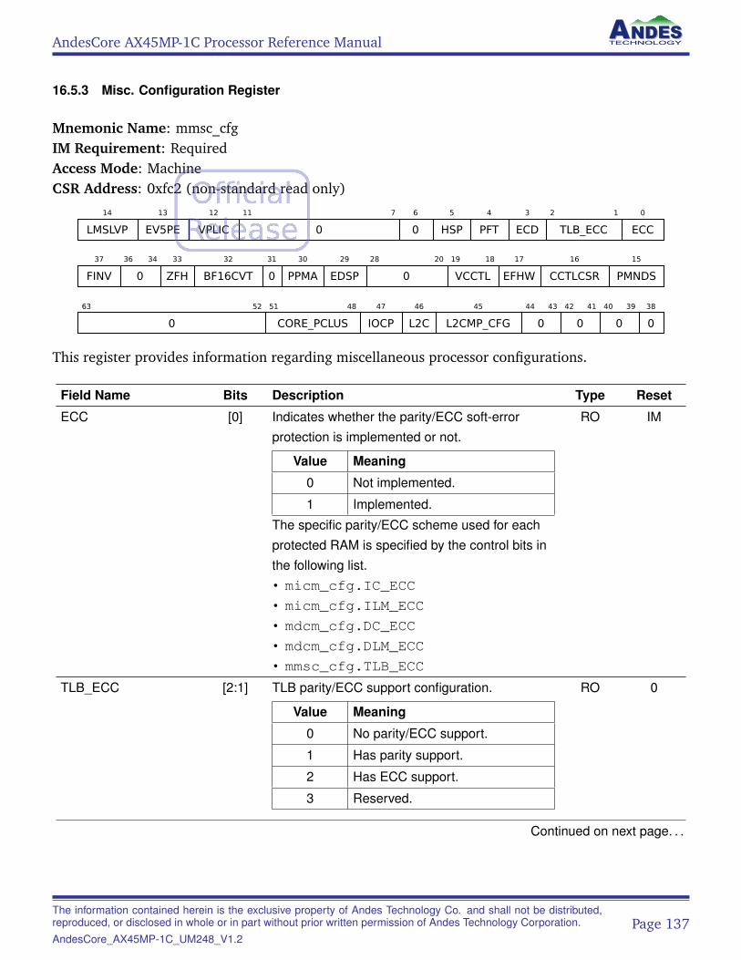
AndesCore AX45MP-1C Processor Reference Manual
16.5.3 Misc. Configuration Register
Mnemonic Name: mmsc_cfgIM Requirement: RequiredAccess Mode: MachineCSR Address: 0xfc2 (non-standard read only)
14
LMSLVP
13
EV5PE
12
VPLIC
11 7
0
6
0
5
HSP
4
PFT
3
ECD
2 1
TLB_ECC
0
ECC
37
FINV
36 34
0
33
ZFH
32
BF16CVT
31
0
30
PPMA
29
EDSP
28 20
0
19 18
VCCTL
17
EFHW
16
CCTLCSR
15
PMNDS
63 52
0
51 48
CORE_PCLUS
47
IOCP
46
L2C
45
L2CMP_CFG
44 43
0
42 41
0
40 39
0
38
0
This register provides information regarding miscellaneous processor configurations.
Field Name Bits Description Type Reset
ECC [0] Indicates whether the parity/ECC soft-errorprotection is implemented or not.
Value Meaning
0 Not implemented.
1 Implemented.
The specific parity/ECC scheme used for eachprotected RAM is specified by the control bits inthe following list.• micm_cfg.IC_ECC• micm_cfg.ILM_ECC• mdcm_cfg.DC_ECC• mdcm_cfg.DLM_ECC• mmsc_cfg.TLB_ECC
RO IM
TLB_ECC [2:1] TLB parity/ECC support configuration.
Value Meaning
0 No parity/ECC support.
1 Has parity support.
2 Has ECC support.
3 Reserved.
RO 0
Continued on next page. . .
The information contained herein is the exclusive property of Andes Technology Co. and shall not be distributed,reproduced, or disclosed in whole or in part without prior written permission of Andes Technology Corporation.AndesCore_AX45MP-1C_UM248_V1.2
Page 137
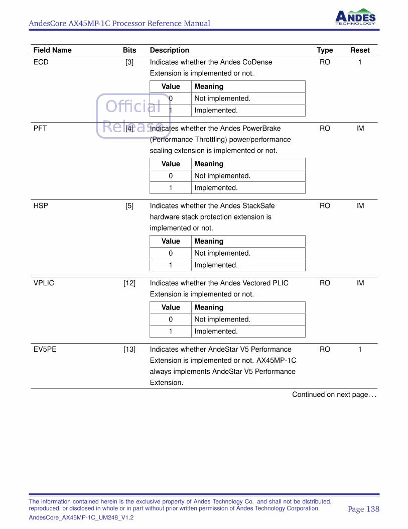
AndesCore AX45MP-1C Processor Reference Manual
Field Name Bits Description Type Reset
ECD [3] Indicates whether the Andes CoDenseExtension is implemented or not.
Value Meaning
0 Not implemented.
1 Implemented.
RO 1
PFT [4] Indicates whether the Andes PowerBrake(Performance Throttling) power/performancescaling extension is implemented or not.
Value Meaning
0 Not implemented.
1 Implemented.
RO IM
HSP [5] Indicates whether the Andes StackSafehardware stack protection extension isimplemented or not.
Value Meaning
0 Not implemented.
1 Implemented.
RO IM
VPLIC [12] Indicates whether the Andes Vectored PLICExtension is implemented or not.
Value Meaning
0 Not implemented.
1 Implemented.
RO IM
EV5PE [13] Indicates whether AndeStar V5 PerformanceExtension is implemented or not. AX45MP-1Calways implements AndeStar V5 PerformanceExtension.
RO 1
Continued on next page. . .
The information contained herein is the exclusive property of Andes Technology Co. and shall not be distributed,reproduced, or disclosed in whole or in part without prior written permission of Andes Technology Corporation.AndesCore_AX45MP-1C_UM248_V1.2
Page 138
AndesCore AX45MP-1C Processor Reference Manual
Field Name Bits Description Type Reset
LMSLVP [14] Indicates if local memory slave port is present ornot.
Value Meaning
0 Local memory slave port is notpresent.
1 Local memory slave port isimplemented.
Note that atomicity of atomic instructionsaccessing local memory address space is notguaranteed if external masters modify the samedata through the local memory slave port.
RO IM
PMNDS [15] Indicates if Andes performance monitorextension is present or not. This extensionshould be present when Performance Monitorsare configured.
Value Meaning
0 Andes-enhanced performancemonitoring feature is notsupported.
1 Andes-enhanced performancemonitoring feature is supported.
RO IM
CCTLCSR [16] Indicates the presence of CSRs for CCTLoperations.
Value Meaning
0 Feature of CSRs for CCTLoperations is not supported.
1 Feature of CSRs for CCTLoperations is supported.
RO IM
Continued on next page. . .
The information contained herein is the exclusive property of Andes Technology Co. and shall not be distributed,reproduced, or disclosed in whole or in part without prior written permission of Andes Technology Corporation.AndesCore_AX45MP-1C_UM248_V1.2
Page 139
AndesCore AX45MP-1C Processor Reference Manual
Field Name Bits Description Type Reset
EFHW [17] Indicates the support of FLHW and FSHWinstructions.
Value Meaning
0 FLHW and FSHW instructions arenot supported.
1 FLHW and FSHW instructions aresupported.
RO IM
VCCTL [19:18] Indicates the version number of CCTL commandoperation scheme supported by animplementation.
Value Meaning
0 Instruction cache and data cacheare not configured.
1 Instruction cache or data cache isconfigured.
RO IM
EDSP [29] Indicates if the DSP extension is supported ornot.
Value Meaning
0 The DSP extension is notsupported.
1 The DSP extension is supported.
RO IM
PPMA [30] Indicates if programmable PMA setup with PMAregion CSRs is supported or not.
Value Meaning
0 Programmable PMA setup is notsupported.
1 Programmable PMA setup issupported.
RO IM
Continued on next page. . .
The information contained herein is the exclusive property of Andes Technology Co. and shall not be distributed,reproduced, or disclosed in whole or in part without prior written permission of Andes Technology Corporation.AndesCore_AX45MP-1C_UM248_V1.2
Page 140
AndesCore AX45MP-1C Processor Reference Manual
Field Name Bits Description Type Reset
BF16CVT [32] Indicates if the BFLOAT16 conversion extensionis supported or not.
Value Meaning
0 The BFLOAT16 conversionextension is not supported
1 The BFLOAT16 conversionextension is supported
RO IM
ZFH [33] Indicates if the FP16 half-precision floating-pointextension (Zfh) is supported or not.
Value Meaning
0 The FP16 extension is notsupported.
1 The FP16 extension is supported.
RO IM
FINV [37] Indicates if scalar FPU is implemented in VPU.
Value Meaning
0 Scalar FPU is not implemented inVPU.
1 Scalar FPU is implemented inVPU.
RO IM
L2CMP_CFG [45] Indicates whether cluster configuration info isimplemented or not.
Value Meaning
0 L2C, IOCP, CORE_PCLUS is notimplemented
1 L2C, IOCP, CORE_PCLUS isimplemented
RO IM
L2C [46] Indicates L2-Cache is present or not.
Value Meaning
0 L2-Cache is not present
1 L2-Cache is present
RO IM
Continued on next page. . .
The information contained herein is the exclusive property of Andes Technology Co. and shall not be distributed,reproduced, or disclosed in whole or in part without prior written permission of Andes Technology Corporation.AndesCore_AX45MP-1C_UM248_V1.2
Page 141
AndesCore AX45MP-1C Processor Reference Manual
Field Name Bits Description Type Reset
IOCP [47] Indicates IO Coherence Port is present or not.
Value Meaning
0 IOCP is not present
1 IOCP is present
RO IM
CORE_PCLUS [51:48] Indicates the number of cores in a cluster
Value Meaning
0 1 core
1 2 cores
3 4 cores
7 8 cores
RO IM
16.5.4 L2-Cache Control Base Register
Mnemonic Name: ml2c_ctl_baseIM Requirement: mmsc_cfg.L2CAccess Mode: MachineCSR Address: 0xfcf (non-standard read only)
63 0
L2C_CTL_BASE
This register indicates the base address of the memory-mapped L2-Cache control registers.
Field Name Bits Description Type Reset
L2C_CTL_BASE [63:0] Indicates L2C Register Base RO IM
The information contained herein is the exclusive property of Andes Technology Co. and shall not be distributed,reproduced, or disclosed in whole or in part without prior written permission of Andes Technology Corporation.AndesCore_AX45MP-1C_UM248_V1.2
Page 142
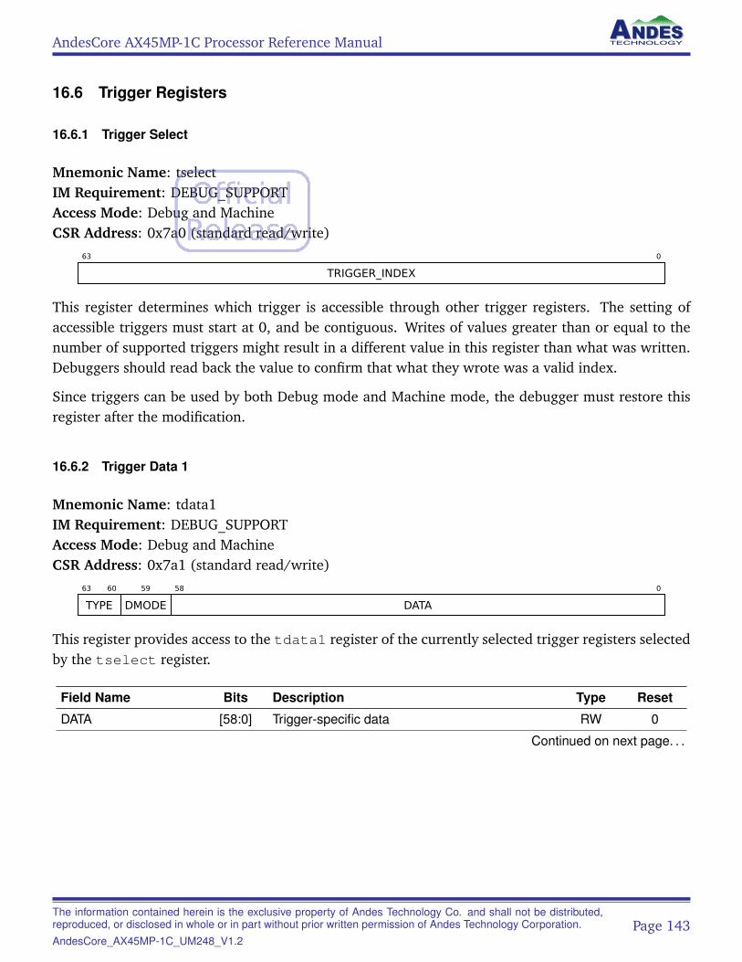
AndesCore AX45MP-1C Processor Reference Manual
16.6 Trigger Registers
16.6.1 Trigger Select
Mnemonic Name: tselectIM Requirement: DEBUG_SUPPORTAccess Mode: Debug and MachineCSR Address: 0x7a0 (standard read/write)
63 0
TRIGGER_INDEX
This register determines which trigger is accessible through other trigger registers. The setting ofaccessible triggers must start at 0, and be contiguous. Writes of values greater than or equal to thenumber of supported triggers might result in a different value in this register than what was written.Debuggers should read back the value to confirm that what they wrote was a valid index.
Since triggers can be used by both Debug mode and Machine mode, the debugger must restore thisregister after the modification.
16.6.2 Trigger Data 1
Mnemonic Name: tdata1IM Requirement: DEBUG_SUPPORTAccess Mode: Debug and MachineCSR Address: 0x7a1 (standard read/write)
63 60
TYPE
59
DMODE
58 0
DATA
This register provides access to the tdata1 register of the currently selected trigger registers selectedby the tselect register.
Field Name Bits Description Type Reset
DATA [58:0] Trigger-specific data RW 0
Continued on next page. . .
The information contained herein is the exclusive property of Andes Technology Co. and shall not be distributed,reproduced, or disclosed in whole or in part without prior written permission of Andes Technology Corporation.AndesCore_AX45MP-1C_UM248_V1.2
Page 143
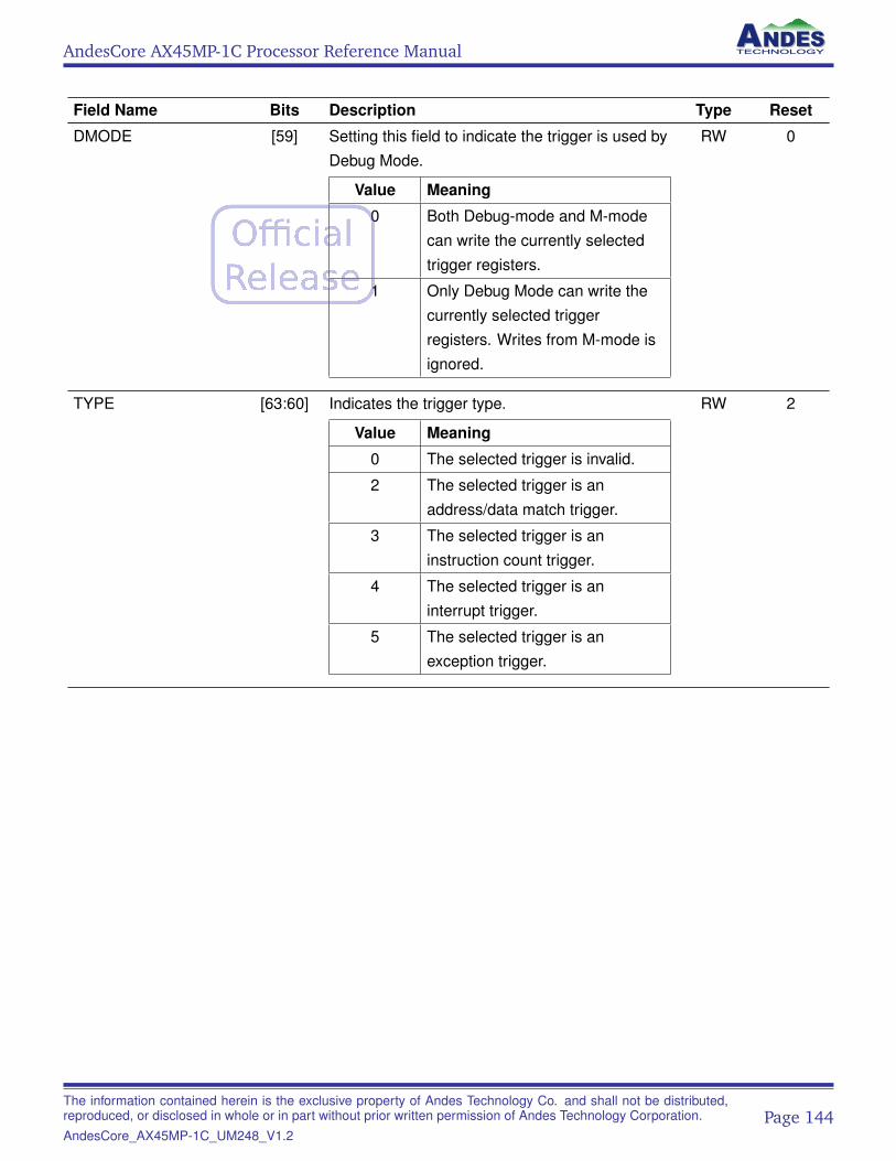
AndesCore AX45MP-1C Processor Reference Manual
Field Name Bits Description Type Reset
DMODE [59] Setting this field to indicate the trigger is used byDebug Mode.
Value Meaning
0 Both Debug-mode and M-modecan write the currently selectedtrigger registers.
1 Only Debug Mode can write thecurrently selected triggerregisters. Writes from M-mode isignored.
RW 0
TYPE [63:60] Indicates the trigger type.
Value Meaning
0 The selected trigger is invalid.
2 The selected trigger is anaddress/data match trigger.
3 The selected trigger is aninstruction count trigger.
4 The selected trigger is aninterrupt trigger.
5 The selected trigger is anexception trigger.
RW 2
The information contained herein is the exclusive property of Andes Technology Co. and shall not be distributed,reproduced, or disclosed in whole or in part without prior written permission of Andes Technology Corporation.AndesCore_AX45MP-1C_UM248_V1.2
Page 144
AndesCore AX45MP-1C Processor Reference Manual
16.6.3 Trigger Data 2
Mnemonic Name: tdata2IM Requirement: DEBUG_SUPPORTAccess Mode: Debug and MachineCSR Address: 0x7a2 (standard read/write)
This register provides accesses to the tdata2 register of the currently selected trigger registers se-lected by the tselect register, and it holds trigger-specific data.
The information contained herein is the exclusive property of Andes Technology Co. and shall not be distributed,reproduced, or disclosed in whole or in part without prior written permission of Andes Technology Corporation.AndesCore_AX45MP-1C_UM248_V1.2
Page 145
AndesCore AX45MP-1C Processor Reference Manual
16.6.4 Trigger Data 3
Mnemonic Name: tdata3IM Requirement: DEBUG_SUPPORTAccess Mode: Debug and MachineCSR Address: 0x7a3 (standard read/write)
This register provides access to the tdata3 register of the currently selected trigger registers selectedby the tselect register, and it holds trigger-specific data.
The information contained herein is the exclusive property of Andes Technology Co. and shall not be distributed,reproduced, or disclosed in whole or in part without prior written permission of Andes Technology Corporation.AndesCore_AX45MP-1C_UM248_V1.2
Page 146
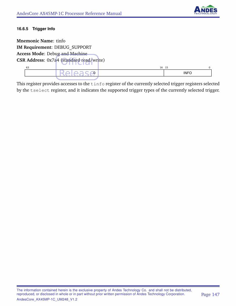
AndesCore AX45MP-1C Processor Reference Manual
16.6.5 Trigger Info
Mnemonic Name: tinfoIM Requirement: DEBUG_SUPPORTAccess Mode: Debug and MachineCSR Address: 0x7a4 (standard read/write)
63 16
0
15 0
INFO
This register provides accesses to the tinfo register of the currently selected trigger registers selectedby the tselect register, and it indicates the supported trigger types of the currently selected trigger.
The information contained herein is the exclusive property of Andes Technology Co. and shall not be distributed,reproduced, or disclosed in whole or in part without prior written permission of Andes Technology Corporation.AndesCore_AX45MP-1C_UM248_V1.2
Page 147
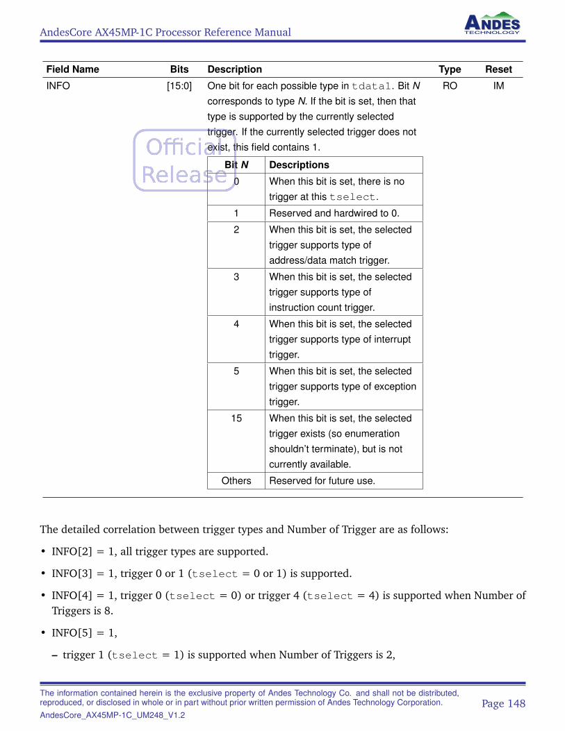
AndesCore AX45MP-1C Processor Reference Manual
Field Name Bits Description Type Reset
INFO [15:0] One bit for each possible type in tdata1. Bit Ncorresponds to type N. If the bit is set, then thattype is supported by the currently selectedtrigger. If the currently selected trigger does notexist, this field contains 1.
Bit N Descriptions
0 When this bit is set, there is notrigger at this tselect.
1 Reserved and hardwired to 0.
2 When this bit is set, the selectedtrigger supports type ofaddress/data match trigger.
3 When this bit is set, the selectedtrigger supports type ofinstruction count trigger.
4 When this bit is set, the selectedtrigger supports type of interrupttrigger.
5 When this bit is set, the selectedtrigger supports type of exceptiontrigger.
15 When this bit is set, the selectedtrigger exists (so enumerationshouldn’t terminate), but is notcurrently available.
Others Reserved for future use.
RO IM
The detailed correlation between trigger types and Number of Trigger are as follows:
• INFO[2] = 1, all trigger types are supported.
• INFO[3] = 1, trigger 0 or 1 (tselect = 0 or 1) is supported.
• INFO[4] = 1, trigger 0 (tselect = 0) or trigger 4 (tselect = 4) is supported when Number ofTriggers is 8.
• INFO[5] = 1,
– trigger 1 (tselect = 1) is supported when Number of Triggers is 2,
The information contained herein is the exclusive property of Andes Technology Co. and shall not be distributed,reproduced, or disclosed in whole or in part without prior written permission of Andes Technology Corporation.AndesCore_AX45MP-1C_UM248_V1.2
Page 148
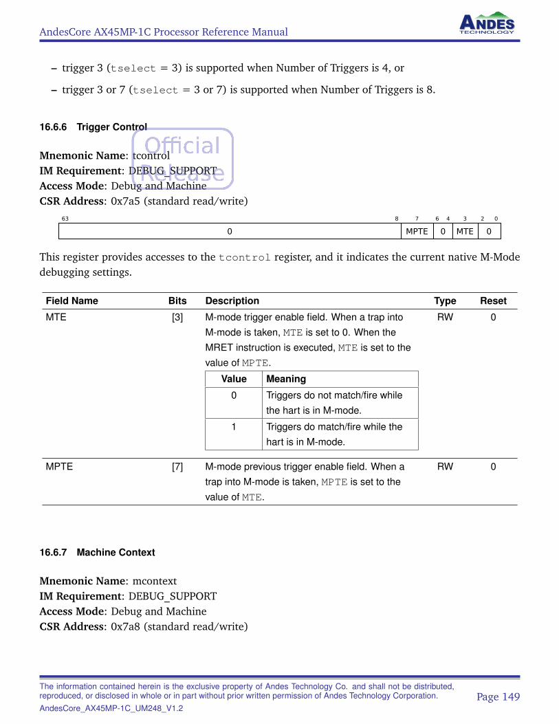
AndesCore AX45MP-1C Processor Reference Manual
– trigger 3 (tselect = 3) is supported when Number of Triggers is 4, or
– trigger 3 or 7 (tselect = 3 or 7) is supported when Number of Triggers is 8.
16.6.6 Trigger Control
Mnemonic Name: tcontrolIM Requirement: DEBUG_SUPPORTAccess Mode: Debug and MachineCSR Address: 0x7a5 (standard read/write)
63 8
0
7
MPTE
6 4
0
3
MTE
2 0
0
This register provides accesses to the tcontrol register, and it indicates the current native M-Modedebugging settings.
Field Name Bits Description Type Reset
MTE [3] M-mode trigger enable field. When a trap intoM-mode is taken, MTE is set to 0. When theMRET instruction is executed, MTE is set to thevalue of MPTE.
Value Meaning
0 Triggers do not match/fire whilethe hart is in M-mode.
1 Triggers do match/fire while thehart is in M-mode.
RW 0
MPTE [7] M-mode previous trigger enable field. When atrap into M-mode is taken, MPTE is set to thevalue of MTE.
RW 0
16.6.7 Machine Context
Mnemonic Name: mcontextIM Requirement: DEBUG_SUPPORTAccess Mode: Debug and MachineCSR Address: 0x7a8 (standard read/write)
The information contained herein is the exclusive property of Andes Technology Co. and shall not be distributed,reproduced, or disclosed in whole or in part without prior written permission of Andes Technology Corporation.AndesCore_AX45MP-1C_UM248_V1.2
Page 149
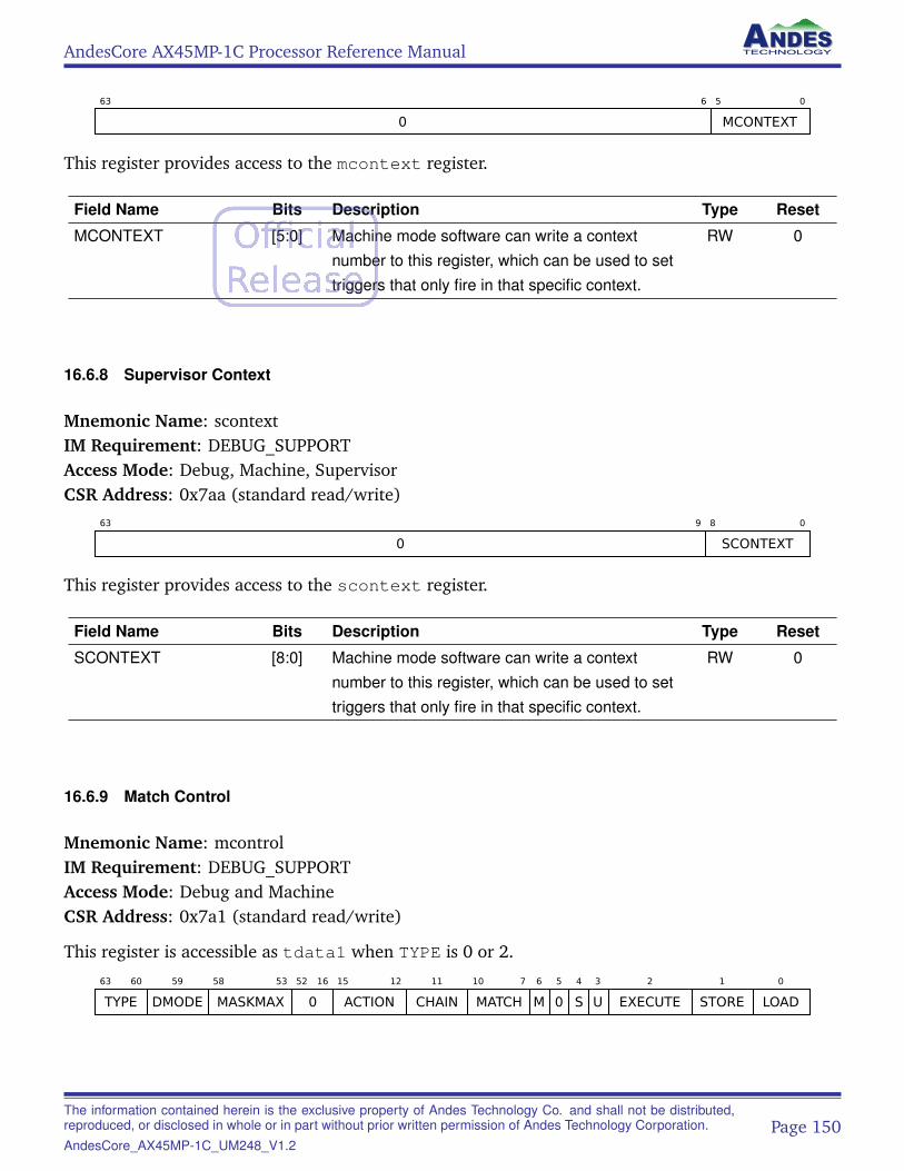
AndesCore AX45MP-1C Processor Reference Manual
63 6
0
5 0
MCONTEXT
This register provides access to the mcontext register.
Field Name Bits Description Type Reset
MCONTEXT [5:0] Machine mode software can write a contextnumber to this register, which can be used to settriggers that only fire in that specific context.
RW 0
16.6.8 Supervisor Context
Mnemonic Name: scontextIM Requirement: DEBUG_SUPPORTAccess Mode: Debug, Machine, SupervisorCSR Address: 0x7aa (standard read/write)
63 9
0
8 0
SCONTEXT
This register provides access to the scontext register.
Field Name Bits Description Type Reset
SCONTEXT [8:0] Machine mode software can write a contextnumber to this register, which can be used to settriggers that only fire in that specific context.
RW 0
16.6.9 Match Control
Mnemonic Name: mcontrolIM Requirement: DEBUG_SUPPORTAccess Mode: Debug and MachineCSR Address: 0x7a1 (standard read/write)
This register is accessible as tdata1 when TYPE is 0 or 2.
63 60
TYPE
59
DMODE
58 53
MASKMAX
52 16
0
15 12
ACTION
11
CHAIN
10 7
MATCH
6
M
5
0
4
S
3
U
2
EXECUTE
1
STORE
0
LOAD
The information contained herein is the exclusive property of Andes Technology Co. and shall not be distributed,reproduced, or disclosed in whole or in part without prior written permission of Andes Technology Corporation.AndesCore_AX45MP-1C_UM248_V1.2
Page 150
AndesCore AX45MP-1C Processor Reference Manual
Field Name Bits Description Type Reset
LOAD [0] Setting this field to enable this trigger tocompare virtual address of a load.
RW* 0
STORE [1] Setting this field to enable this trigger tocompare virtual address of a store.
RW* 0
EXECUTE [2] Setting this field to enable this trigger tocompare virtual address of an instruction.
RW 0
U [3] Setting this field to enable this trigger in U-mode. RW 0
S [4] Setting this field to enable this trigger in S-mode. RW 0
M [6] Setting this field to enable this trigger in M-mode. RW 0
MATCH [10:7] Setting this field to select the matching scheme.
Value Meaning
0 Matches when the value equalstdata2.
1 Matches when the top M bits ofthe value match the top M bits oftdata2. M is 63 minus theindex of the least-significant bitcontaining 0 in tdata2.
2 Matches when the value isgreater than (unsigned) or equalto tdata2.
3 Matches when the value is lessthan (unsigned) tdata2.
RW 0
Continued on next page. . .
The information contained herein is the exclusive property of Andes Technology Co. and shall not be distributed,reproduced, or disclosed in whole or in part without prior written permission of Andes Technology Corporation.AndesCore_AX45MP-1C_UM248_V1.2
Page 151
AndesCore AX45MP-1C Processor Reference Manual
Field Name Bits Description Type Reset
CHAIN [11] Setting this field to enable trigger chain.
Value Meaning
0 When this trigger matches, theconfigured action is taken.
1 While this trigger does not match,it prevents the trigger with thenext index from matching.
If Number of Triggers is 2, this field is hardwiredto 0 on trigger 1 (tselect = 1).If Number of Triggers is 4, this field is hardwiredto 0 on trigger 3 (tselect = 3).If Number of Triggers is 8, this field is hardwiredto 0 on trigger 3 and trigger 7 (tselect = 3 or7).
RW 0
ACTION [15:12] Setting this field to select what happens whenthis trigger matches.
Value Meaning
0 Raise a breakpoint exception.
1 Enter Debug Mode. (Onlysupported when DMODE is 1.)
RW 0
MASKMAX [58:53] Indicates the largest naturally aligned rangesupported by the hardware is 2ˆ12 bytes.
RO 12
DMODE [59] Setting this field to indicate the trigger is used byDebug Mode.
Value Meaning
0 Both Debug-mode and M-modecan write the currently selectedtrigger registers.
1 Only Debug Mode can write thecurrently selected triggerregisters. Writes from M-mode isignored.
RW 0
Continued on next page. . .
The information contained herein is the exclusive property of Andes Technology Co. and shall not be distributed,reproduced, or disclosed in whole or in part without prior written permission of Andes Technology Corporation.AndesCore_AX45MP-1C_UM248_V1.2
Page 152
AndesCore AX45MP-1C Processor Reference Manual
Field Name Bits Description Type Reset
TYPE [63:60] Indicates the trigger type.
Value Meaning
0 The selected trigger is invalid.
2 The selected trigger is anaddress/data match trigger.
RW 2
NoteThe LOAD/STORE fields take no effect and are cleared if the EXECUTE field is set at the same time.
16.6.10 Instruction Count
Mnemonic Name: icountIM Requirement: DEBUG_SUPPORTAccess Mode: Debug and MachineCSR Address: 0x7a1 (standard read/write)
This register is accessible as tdata1 when TYPE is 3.
This register exists just for single-stepping support so COUNT is hardwired to 1. After this triggerfires, the mode bits the mode bits (M, S, U) will be cleared instead of causing the COUNT bits to bedecremented.
63 60
TYPE
59
DMODE
58 11
0
10
COUNT
9
M
8
0
7
S
6
U
5 0
ACTION
Field Name Bits Description Type Reset
ACTION [5:0] Setting this field to select what happens whenthis trigger matches.
Value Meaning
0 Raise a breakpoint exception.
1 Enter Debug Mode. (Onlysupported when DMODE is 1.)
RW 0
U [6] Setting this field to enable this trigger in U-mode. RW 0
S [7] Setting this field to enable this trigger in S-mode. RW 0
M [9] Setting this field to enable this trigger in M-mode. RW 0
Continued on next page. . .
The information contained herein is the exclusive property of Andes Technology Co. and shall not be distributed,reproduced, or disclosed in whole or in part without prior written permission of Andes Technology Corporation.AndesCore_AX45MP-1C_UM248_V1.2
Page 153
AndesCore AX45MP-1C Processor Reference Manual
Field Name Bits Description Type Reset
COUNT [10] This field is hardwired to 1 for single-steppingsupport
RO 1
DMODE [59] Setting this field to indicate the trigger is used byDebug Mode.
Value Meaning
0 Both Debug-mode and M-modecan write the currently selectedtrigger registers.
1 Only Debug Mode can write thecurrently selected triggerregisters. Writes from M-mode isignored.
RW 0
TYPE [63:60] The selected trigger is an instruction counttrigger.
RW 2
16.6.11 Interrupt Trigger
Mnemonic Name: itriggerIM Requirement: DEBUG_SUPPORTAccess Mode: Debug and MachineCSR Address: 0x7a1 (standard read/write)
This register is accessible as tdata1 when TYPE is 4.
This trigger may fire on any of the interrupts configurable in mie. The interrupts to fire on areconfigured by setting the same bit in tdata2 as would be set in mie to enable the interrupt.
63 60
TYPE
59
DMODE
58 10
0
9
M
8
0
7
S
6
U
5 0
ACTION
The information contained herein is the exclusive property of Andes Technology Co. and shall not be distributed,reproduced, or disclosed in whole or in part without prior written permission of Andes Technology Corporation.AndesCore_AX45MP-1C_UM248_V1.2
Page 154
AndesCore AX45MP-1C Processor Reference Manual
Field Name Bits Description Type Reset
ACTION [5:0] Setting this field to select what happens whenthis trigger matches.
Value Meaning
0 Raise a breakpoint exception.
1 Enter Debug Mode. (Onlysupported when DMODE is 1.)
RW 0
U [6] Setting this field to enable this trigger in U-mode. RW 0
S [7] Setting this field to enable this trigger in S-mode. RW 0
M [9] Setting this field to enable this trigger in M-mode. RW 0
DMODE [59] Setting this field to indicate the trigger is used byDebug Mode.
Value Meaning
0 Both Debug-mode and M-modecan write the currently selectedtrigger registers.
1 Only Debug Mode can write thecurrently selected triggerregisters. Writes from M-mode isignored.
RW 0
TYPE [63:60] The selected trigger is an interrupt trigger. RW 2
The information contained herein is the exclusive property of Andes Technology Co. and shall not be distributed,reproduced, or disclosed in whole or in part without prior written permission of Andes Technology Corporation.AndesCore_AX45MP-1C_UM248_V1.2
Page 155
AndesCore AX45MP-1C Processor Reference Manual
16.6.12 Exception Trigger
Mnemonic Name: etriggerIM Requirement: DEBUG_SUPPORTAccess Mode: Debug and MachineCSR Address: 0x7a1 (standard read/write)
This register is accessible as tdata1 when TYPE is 5.
This trigger may fire on up to XLEN of the Exception Codes defined in mcause (with Interrupt=0).Those causes are configured by writing the corresponding bit in tdata2. (E.g. to trap on an illegalinstruction, the debugger sets bit 2 in tdata2.)
63 60
TYPE
59
DMODE
58 11
0
10
NMI
9
M
8
0
7
S
6
U
5 0
ACTION
Field Name Bits Description Type Reset
ACTION [5:0] Setting this field to select what happens whenthis trigger matches.
Value Meaning
0 Raise a breakpoint exception.
1 Enter Debug Mode. (Onlysupported when DMODE is 1.)
RW 0
U [6] Setting this field to enable this trigger in U-mode. RW 0
S [7] Setting this field to enable this trigger in S-mode. RW 0
M [9] Setting this field to enable this trigger in M-mode. RW 0
NMI [10] Setting this field to enable this trigger innon-maskable interrupts, regardless of thevalues of s, u, and m.
RW 0
Continued on next page. . .
The information contained herein is the exclusive property of Andes Technology Co. and shall not be distributed,reproduced, or disclosed in whole or in part without prior written permission of Andes Technology Corporation.AndesCore_AX45MP-1C_UM248_V1.2
Page 156
AndesCore AX45MP-1C Processor Reference Manual
Field Name Bits Description Type Reset
DMODE [59] Setting this field to indicate the trigger is used byDebug Mode.
Value Meaning
0 Both Debug-mode and M-modecan write the currently selectedtrigger registers.
1 Only Debug Mode can write thecurrently selected triggerregisters. Writes from M-mode isignored.
RW 0
TYPE [63:60] The selected trigger is an exception trigger. RW 2
The information contained herein is the exclusive property of Andes Technology Co. and shall not be distributed,reproduced, or disclosed in whole or in part without prior written permission of Andes Technology Corporation.AndesCore_AX45MP-1C_UM248_V1.2
Page 157
AndesCore AX45MP-1C Processor Reference Manual
16.6.13 Trigger Extra
Mnemonic Name: textraIM Requirement: DEBUG_SUPPORTAccess Mode: Debug and MachineCSR Address: 0x7a3 (standard read/write)
This register is accessible as tdata3 when TYPE is 2, 3, 4, or 5 of the currently selected trigger regis-ters selected by the tselect register, and it indicates the context matching scheme of the currentlyselected trigger.
63 57
0
56 51
MVALUE
50
MSELECT
49 11
0
10 2
SVALUE
1 0
SSELECT
Field Name Bits Description Type Reset
SSELECT [1:0]
Value Meaning
0 Ignore MVALUE.
1 This trigger will only match if thelower bits of scontext equalSVALUE.
2 This trigger will only match ifsatp.ASID equals SVALUE.
RW 0
SVALUE [10:2] Data used together with SSELECT. RW 0
MSELECT [50]
Value Meaning
0 Ignore MVALUE.
1 This trigger will only match if thelower bits of mcontext equalMVALUE.
RW 0
MVALUE [56:51] Data used together with MSELECT. RW 0
The information contained herein is the exclusive property of Andes Technology Co. and shall not be distributed,reproduced, or disclosed in whole or in part without prior written permission of Andes Technology Corporation.AndesCore_AX45MP-1C_UM248_V1.2
Page 158
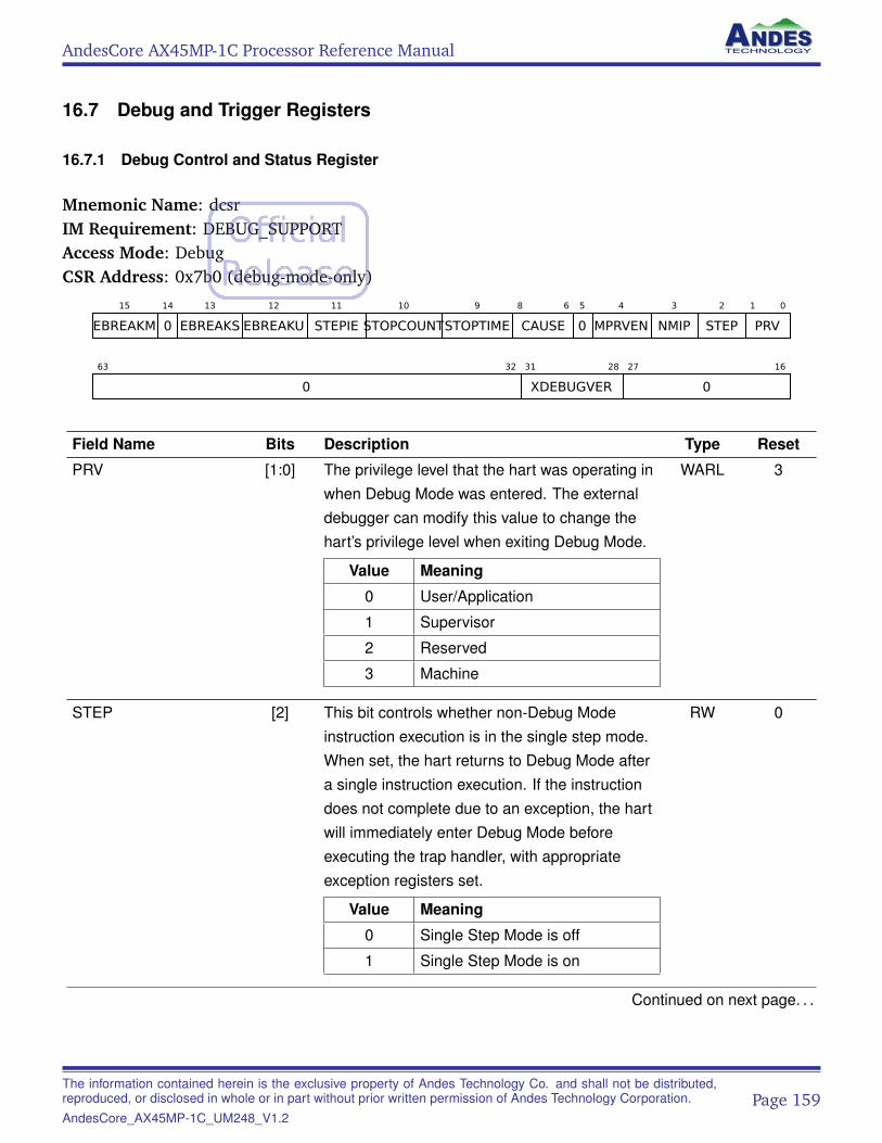
AndesCore AX45MP-1C Processor Reference Manual
16.7 Debug and Trigger Registers
16.7.1 Debug Control and Status Register
Mnemonic Name: dcsrIM Requirement: DEBUG_SUPPORTAccess Mode: DebugCSR Address: 0x7b0 (debug-mode-only)
15
EBREAKM
14
0
13
EBREAKS
12
EBREAKU
11
STEPIE
10
STOPCOUNT
9
STOPTIME
8 6
CAUSE
5
0
4
MPRVEN
3
NMIP
2
STEP
1 0
PRV
63 32
0
31 28
XDEBUGVER
27 16
0
Field Name Bits Description Type Reset
PRV [1:0] The privilege level that the hart was operating inwhen Debug Mode was entered. The externaldebugger can modify this value to change thehart’s privilege level when exiting Debug Mode.
Value Meaning
0 User/Application
1 Supervisor
2 Reserved
3 Machine
WARL 3
STEP [2] This bit controls whether non-Debug Modeinstruction execution is in the single step mode.When set, the hart returns to Debug Mode aftera single instruction execution. If the instructiondoes not complete due to an exception, the hartwill immediately enter Debug Mode beforeexecuting the trap handler, with appropriateexception registers set.
Value Meaning
0 Single Step Mode is off
1 Single Step Mode is on
RW 0
Continued on next page. . .
The information contained herein is the exclusive property of Andes Technology Co. and shall not be distributed,reproduced, or disclosed in whole or in part without prior written permission of Andes Technology Corporation.AndesCore_AX45MP-1C_UM248_V1.2
Page 159
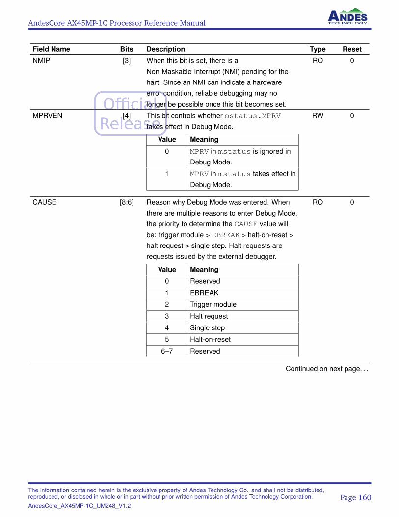
AndesCore AX45MP-1C Processor Reference Manual
Field Name Bits Description Type Reset
NMIP [3] When this bit is set, there is aNon-Maskable-Interrupt (NMI) pending for thehart. Since an NMI can indicate a hardwareerror condition, reliable debugging may nolonger be possible once this bit becomes set.
RO 0
MPRVEN [4] This bit controls whether mstatus.MPRVtakes effect in Debug Mode.
Value Meaning
0 MPRV in mstatus is ignored inDebug Mode.
1 MPRV in mstatus takes effect inDebug Mode.
RW 0
CAUSE [8:6] Reason why Debug Mode was entered. Whenthere are multiple reasons to enter Debug Mode,the priority to determine the CAUSE value willbe: trigger module > EBREAK > halt-on-reset >halt request > single step. Halt requests arerequests issued by the external debugger.
Value Meaning
0 Reserved
1 EBREAK
2 Trigger module
3 Halt request
4 Single step
5 Halt-on-reset
6–7 Reserved
RO 0
Continued on next page. . .
The information contained herein is the exclusive property of Andes Technology Co. and shall not be distributed,reproduced, or disclosed in whole or in part without prior written permission of Andes Technology Corporation.AndesCore_AX45MP-1C_UM248_V1.2
Page 160
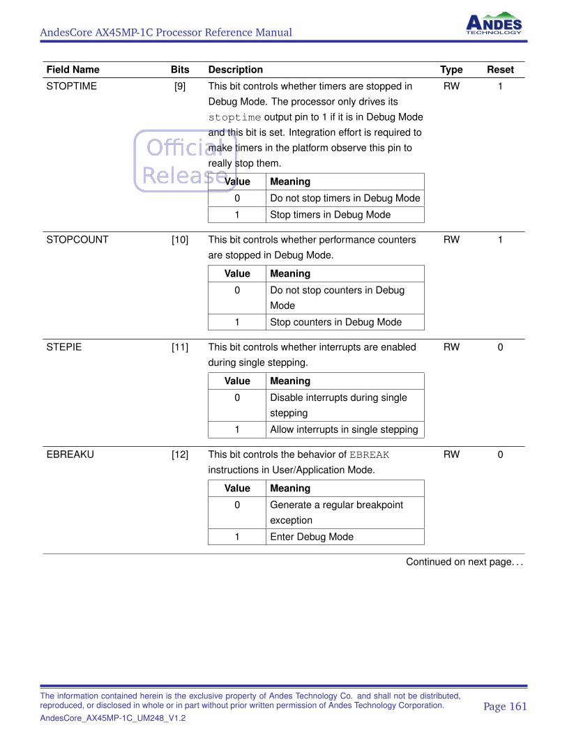
AndesCore AX45MP-1C Processor Reference Manual
Field Name Bits Description Type Reset
STOPTIME [9] This bit controls whether timers are stopped inDebug Mode. The processor only drives itsstoptime output pin to 1 if it is in Debug Modeand this bit is set. Integration effort is required tomake timers in the platform observe this pin toreally stop them.
Value Meaning
0 Do not stop timers in Debug Mode
1 Stop timers in Debug Mode
RW 1
STOPCOUNT [10] This bit controls whether performance countersare stopped in Debug Mode.
Value Meaning
0 Do not stop counters in DebugMode
1 Stop counters in Debug Mode
RW 1
STEPIE [11] This bit controls whether interrupts are enabledduring single stepping.
Value Meaning
0 Disable interrupts during singlestepping
1 Allow interrupts in single stepping
RW 0
EBREAKU [12] This bit controls the behavior of EBREAKinstructions in User/Application Mode.
Value Meaning
0 Generate a regular breakpointexception
1 Enter Debug Mode
RW 0
Continued on next page. . .
The information contained herein is the exclusive property of Andes Technology Co. and shall not be distributed,reproduced, or disclosed in whole or in part without prior written permission of Andes Technology Corporation.AndesCore_AX45MP-1C_UM248_V1.2
Page 161
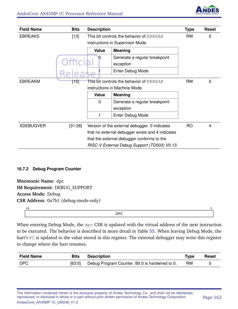
AndesCore AX45MP-1C Processor Reference Manual
Field Name Bits Description Type Reset
EBREAKS [13] This bit controls the behavior of EBREAKinstructions in Supervisor Mode.
Value Meaning
0 Generate a regular breakpointexception
1 Enter Debug Mode
RW 0
EBREAKM [15] This bit controls the behavior of EBREAKinstructions in Machine Mode.
Value Meaning
0 Generate a regular breakpointexception
1 Enter Debug Mode
RW 0
XDEBUGVER [31:28] Version of the external debugger. 0 indicatesthat no external debugger exists and 4 indicatesthat the external debugger conforms to theRISC-V External Debug Support (TD003) V0.13.
RO 4
16.7.2 Debug Program Counter
Mnemonic Name: dpcIM Requirement: DEBUG_SUPPORTAccess Mode: DebugCSR Address: 0x7b1 (debug-mode-only)
63 0
DPC
When entering Debug Mode, the dpc CSR is updated with the virtual address of the next instructionto be executed. The behavior is described in more detail in Table 55. When leaving Debug Mode, thehart’s PC is updated to the value stored in this register. The external debugger may write this registerto change where the hart resumes.
Field Name Bits Description Type Reset
DPC [63:0] Debug Program Counter. Bit 0 is hardwired to 0. RW 0
The information contained herein is the exclusive property of Andes Technology Co. and shall not be distributed,reproduced, or disclosed in whole or in part without prior written permission of Andes Technology Corporation.AndesCore_AX45MP-1C_UM248_V1.2
Page 162
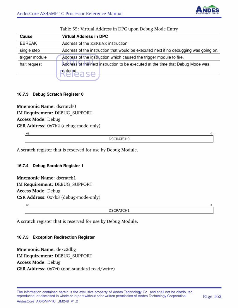
AndesCore AX45MP-1C Processor Reference Manual
Table 55: Virtual Address in DPC upon Debug Mode Entry
Cause Virtual Address in DPC
EBREAK Address of the EBREAK instruction
single step Address of the instruction that would be executed next if no debugging was going on.
trigger module Address of the instruction which caused the trigger module to fire.
halt request Address of the next instruction to be executed at the time that Debug Mode wasentered
16.7.3 Debug Scratch Register 0
Mnemonic Name: dscratch0IM Requirement: DEBUG_SUPPORTAccess Mode: DebugCSR Address: 0x7b2 (debug-mode-only)
63 0
DSCRATCH0
A scratch register that is reserved for use by Debug Module.
16.7.4 Debug Scratch Register 1
Mnemonic Name: dscratch1IM Requirement: DEBUG_SUPPORTAccess Mode: DebugCSR Address: 0x7b3 (debug-mode-only)
63 0
DSCRATCH1
A scratch register that is reserved for use by Debug Module.
16.7.5 Exception Redirection Register
Mnemonic Name: dexc2dbgIM Requirement: DEBUG_SUPPORTAccess Mode: DebugCSR Address: 0x7e0 (non-standard read/write)
The information contained herein is the exclusive property of Andes Technology Co. and shall not be distributed,reproduced, or disclosed in whole or in part without prior written permission of Andes Technology Corporation.AndesCore_AX45MP-1C_UM248_V1.2
Page 163
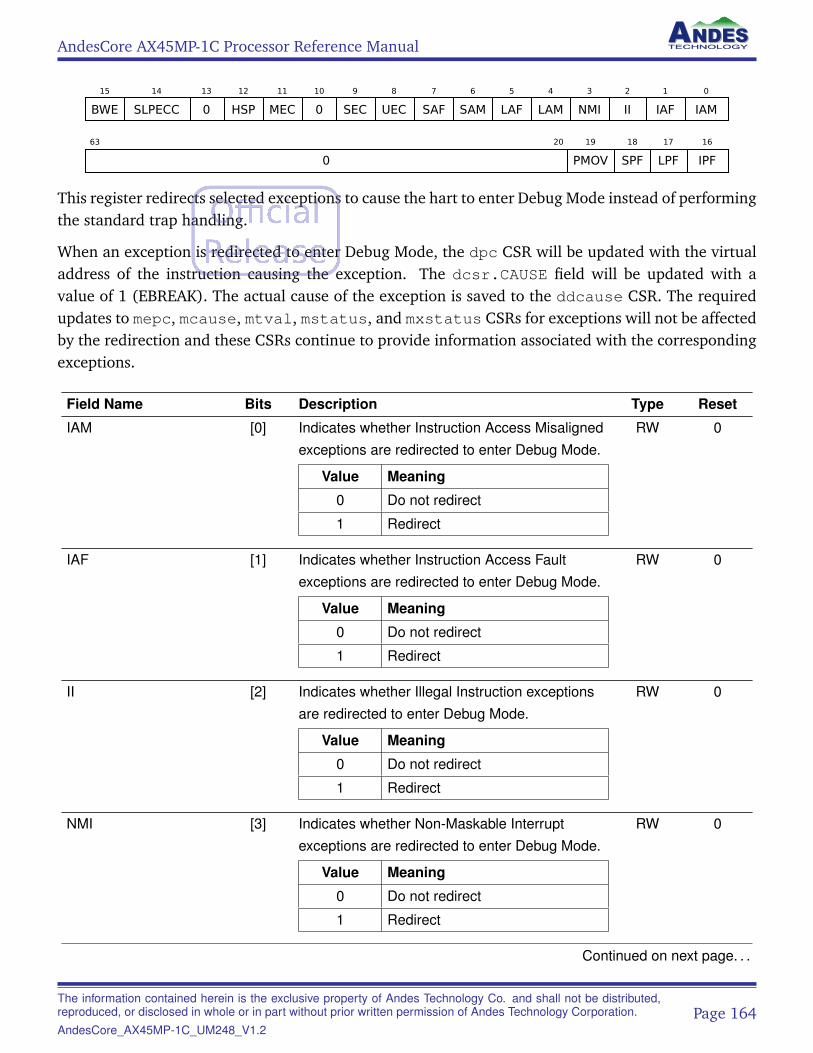
AndesCore AX45MP-1C Processor Reference Manual
15
BWE
14
SLPECC
13
0
12
HSP
11
MEC
10
0
9
SEC
8
UEC
7
SAF
6
SAM
5
LAF
4
LAM
3
NMI
2
II
1
IAF
0
IAM
63 20
0
19
PMOV
18
SPF
17
LPF
16
IPF
This register redirects selected exceptions to cause the hart to enter Debug Mode instead of performingthe standard trap handling.
When an exception is redirected to enter Debug Mode, the dpc CSR will be updated with the virtualaddress of the instruction causing the exception. The dcsr.CAUSE field will be updated with avalue of 1 (EBREAK). The actual cause of the exception is saved to the ddcause CSR. The requiredupdates to mepc, mcause, mtval, mstatus, and mxstatus CSRs for exceptions will not be affectedby the redirection and these CSRs continue to provide information associated with the correspondingexceptions.
Field Name Bits Description Type Reset
IAM [0] Indicates whether Instruction Access Misalignedexceptions are redirected to enter Debug Mode.
Value Meaning
0 Do not redirect
1 Redirect
RW 0
IAF [1] Indicates whether Instruction Access Faultexceptions are redirected to enter Debug Mode.
Value Meaning
0 Do not redirect
1 Redirect
RW 0
II [2] Indicates whether Illegal Instruction exceptionsare redirected to enter Debug Mode.
Value Meaning
0 Do not redirect
1 Redirect
RW 0
NMI [3] Indicates whether Non-Maskable Interruptexceptions are redirected to enter Debug Mode.
Value Meaning
0 Do not redirect
1 Redirect
RW 0
Continued on next page. . .
The information contained herein is the exclusive property of Andes Technology Co. and shall not be distributed,reproduced, or disclosed in whole or in part without prior written permission of Andes Technology Corporation.AndesCore_AX45MP-1C_UM248_V1.2
Page 164
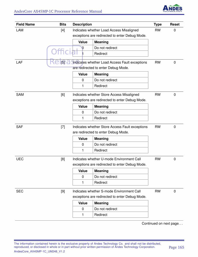
AndesCore AX45MP-1C Processor Reference Manual
Field Name Bits Description Type Reset
LAM [4] Indicates whether Load Access Misalignedexceptions are redirected to enter Debug Mode.
Value Meaning
0 Do not redirect
1 Redirect
RW 0
LAF [5] Indicates whether Load Access Fault exceptionsare redirected to enter Debug Mode.
Value Meaning
0 Do not redirect
1 Redirect
RW 0
SAM [6] Indicates whether Store Access Misalignedexceptions are redirected to enter Debug Mode.
Value Meaning
0 Do not redirect
1 Redirect
RW 0
SAF [7] Indicates whether Store Access Fault exceptionsare redirected to enter Debug Mode.
Value Meaning
0 Do not redirect
1 Redirect
RW 0
UEC [8] Indicates whether U-mode Environment Callexceptions are redirected to enter Debug Mode.
Value Meaning
0 Do not redirect
1 Redirect
RW 0
SEC [9] Indicates whether S-mode Environment Callexceptions are redirected to enter Debug Mode.
Value Meaning
0 Do not redirect
1 Redirect
RW 0
Continued on next page. . .
The information contained herein is the exclusive property of Andes Technology Co. and shall not be distributed,reproduced, or disclosed in whole or in part without prior written permission of Andes Technology Corporation.AndesCore_AX45MP-1C_UM248_V1.2
Page 165

AndesCore AX45MP-1C Processor Reference Manual
Field Name Bits Description Type Reset
MEC [11] Indicates whether M-mode Environment Callexceptions are redirected to enter Debug Mode.
Value Meaning
0 Do not redirect
1 Redirect
RW 0
HSP [12] Indicates whether Stack Protection exceptionsare redirected to enter Debug Mode. This bit ispresent only when mmsc_cfg.HSP is set.
Value Meaning
0 Do not redirect
1 Redirect
RW 0
SLPECC [14] Indicates whether local memory slave port ECCError local interrupts are redirected to enterDebug Mode.
Value Meaning
0 Do not redirect
1 Redirect
RW 0
BWE [15] Indicates whether Bus-write Transaction Errorlocal interrupts are redirected to enter DebugMode.
Value Meaning
0 Do not redirect
1 Redirect
RW 0
IPF [16] Indicates whether instruction page faultexceptions are redirected to enter Debug Mode.
Value Meaning
0 Do not redirect
1 Redirect
RW 0
Continued on next page. . .
The information contained herein is the exclusive property of Andes Technology Co. and shall not be distributed,reproduced, or disclosed in whole or in part without prior written permission of Andes Technology Corporation.AndesCore_AX45MP-1C_UM248_V1.2
Page 166
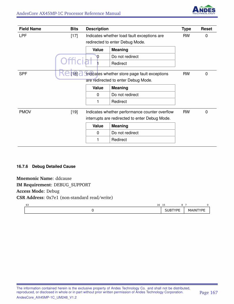
AndesCore AX45MP-1C Processor Reference Manual
Field Name Bits Description Type Reset
LPF [17] Indicates whether load fault exceptions areredirected to enter Debug Mode.
Value Meaning
0 Do not redirect
1 Redirect
RW 0
SPF [18] Indicates whether store page fault exceptionsare redirected to enter Debug Mode.
Value Meaning
0 Do not redirect
1 Redirect
RW 0
PMOV [19] Indicates whether performance counter overflowinterrupts are redirected to enter Debug Mode.
Value Meaning
0 Do not redirect
1 Redirect
RW 0
16.7.6 Debug Detailed Cause
Mnemonic Name: ddcauseIM Requirement: DEBUG_SUPPORTAccess Mode: DebugCSR Address: 0x7e1 (non-standard read/write)
63 16
0
15 8
SUBTYPE
7 0
MAINTYPE
The information contained herein is the exclusive property of Andes Technology Co. and shall not be distributed,reproduced, or disclosed in whole or in part without prior written permission of Andes Technology Corporation.AndesCore_AX45MP-1C_UM248_V1.2
Page 167
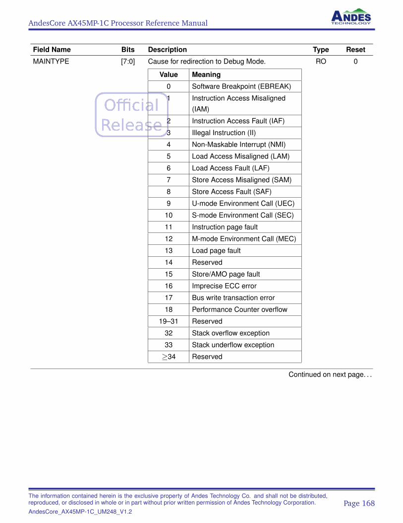
AndesCore AX45MP-1C Processor Reference Manual
Field Name Bits Description Type Reset
MAINTYPE [7:0] Cause for redirection to Debug Mode.
Value Meaning
0 Software Breakpoint (EBREAK)
1 Instruction Access Misaligned(IAM)
2 Instruction Access Fault (IAF)
3 Illegal Instruction (II)
4 Non-Maskable Interrupt (NMI)
5 Load Access Misaligned (LAM)
6 Load Access Fault (LAF)
7 Store Access Misaligned (SAM)
8 Store Access Fault (SAF)
9 U-mode Environment Call (UEC)
10 S-mode Environment Call (SEC)
11 Instruction page fault
12 M-mode Environment Call (MEC)
13 Load page fault
14 Reserved
15 Store/AMO page fault
16 Imprecise ECC error
17 Bus write transaction error
18 Performance Counter overflow
19–31 Reserved
32 Stack overflow exception
33 Stack underflow exception
≥34 Reserved
RO 0
Continued on next page. . .
The information contained herein is the exclusive property of Andes Technology Co. and shall not be distributed,reproduced, or disclosed in whole or in part without prior written permission of Andes Technology Corporation.AndesCore_AX45MP-1C_UM248_V1.2
Page 168
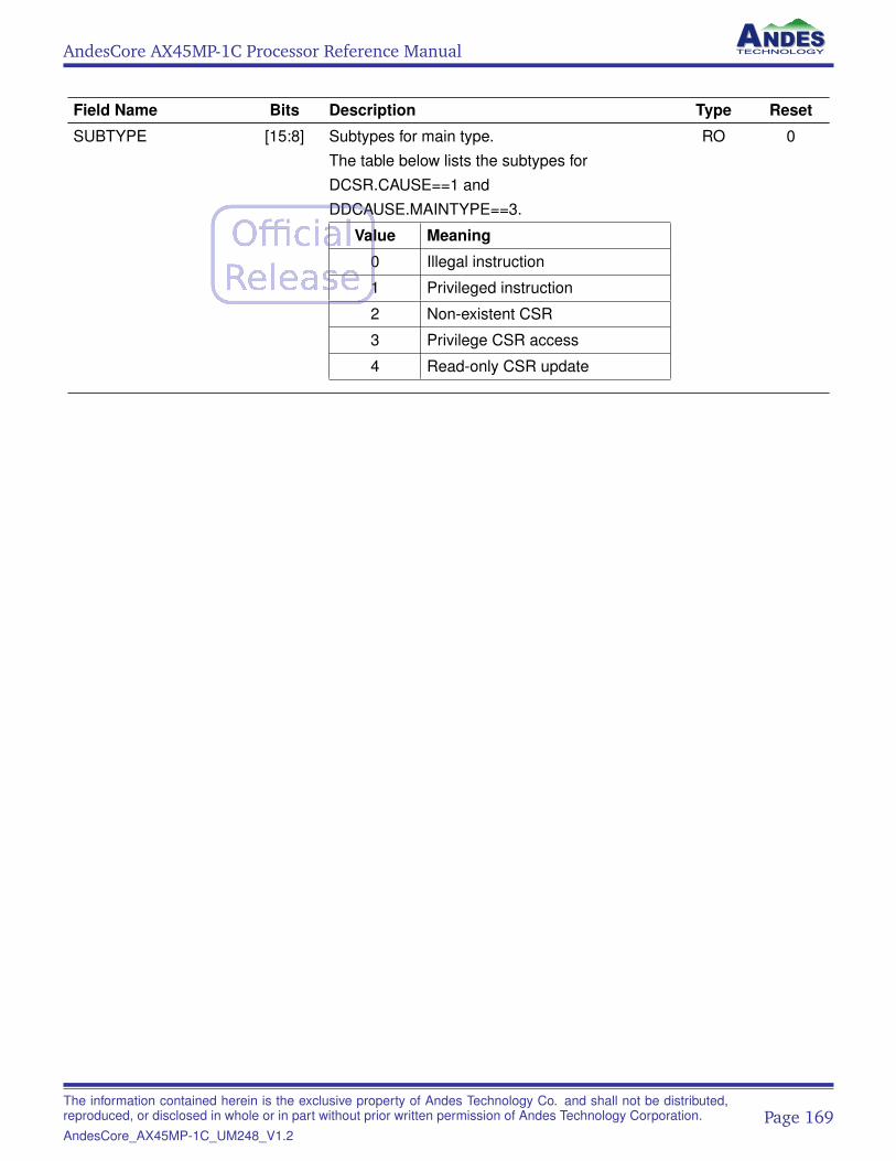
AndesCore AX45MP-1C Processor Reference Manual
Field Name Bits Description Type Reset
SUBTYPE [15:8] Subtypes for main type.The table below lists the subtypes forDCSR.CAUSE==1 andDDCAUSE.MAINTYPE==3.
Value Meaning
0 Illegal instruction
1 Privileged instruction
2 Non-existent CSR
3 Privilege CSR access
4 Read-only CSR update
RO 0
The information contained herein is the exclusive property of Andes Technology Co. and shall not be distributed,reproduced, or disclosed in whole or in part without prior written permission of Andes Technology Corporation.AndesCore_AX45MP-1C_UM248_V1.2
Page 169
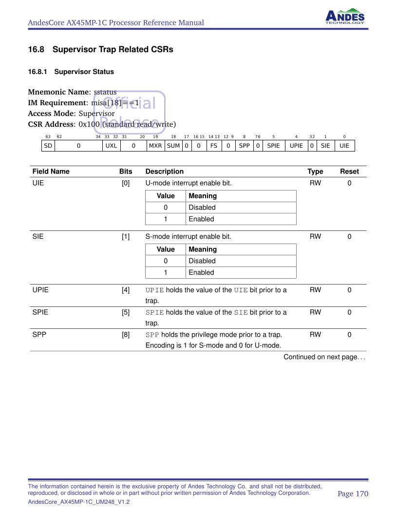
AndesCore AX45MP-1C Processor Reference Manual
16.8 Supervisor Trap Related CSRs
16.8.1 Supervisor Status
Mnemonic Name: sstatusIM Requirement: misa[18]==1Access Mode: SupervisorCSR Address: 0x100 (standard read/write)
63
SD
62 34
0
33 32
UXL
31 20
0
19
MXR
18
SUM
17
0
16 15
0
14 13
FS
12 9
0
8
SPP
76
0
5
SPIE
4
UPIE
32
0
1
SIE
0
UIE
Field Name Bits Description Type Reset
UIE [0] U-mode interrupt enable bit.
Value Meaning
0 Disabled
1 Enabled
RW 0
SIE [1] S-mode interrupt enable bit.
Value Meaning
0 Disabled
1 Enabled
RW 0
UPIE [4] UPIE holds the value of the UIE bit prior to atrap.
RW 0
SPIE [5] SPIE holds the value of the SIE bit prior to atrap.
RW 0
SPP [8] SPP holds the privilege mode prior to a trap.Encoding is 1 for S-mode and 0 for U-mode.
RW 0
Continued on next page. . .
The information contained herein is the exclusive property of Andes Technology Co. and shall not be distributed,reproduced, or disclosed in whole or in part without prior written permission of Andes Technology Corporation.AndesCore_AX45MP-1C_UM248_V1.2
Page 170
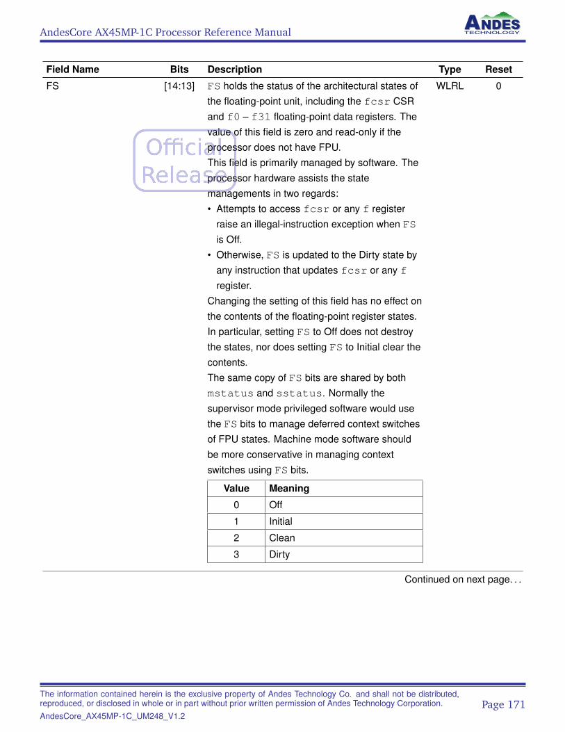
AndesCore AX45MP-1C Processor Reference Manual
Field Name Bits Description Type Reset
FS [14:13] FS holds the status of the architectural states ofthe floating-point unit, including the fcsr CSRand f0 – f31 floating-point data registers. Thevalue of this field is zero and read-only if theprocessor does not have FPU.This field is primarily managed by software. Theprocessor hardware assists the statemanagements in two regards:• Attempts to access fcsr or any f register
raise an illegal-instruction exception when FSis Off.
• Otherwise, FS is updated to the Dirty state byany instruction that updates fcsr or any fregister.
Changing the setting of this field has no effect onthe contents of the floating-point register states.In particular, setting FS to Off does not destroythe states, nor does setting FS to Initial clear thecontents.The same copy of FS bits are shared by bothmstatus and sstatus. Normally thesupervisor mode privileged software would usethe FS bits to manage deferred context switchesof FPU states. Machine mode software shouldbe more conservative in managing contextswitches using FS bits.
Value Meaning
0 Off
1 Initial
2 Clean
3 Dirty
WLRL 0
Continued on next page. . .
The information contained herein is the exclusive property of Andes Technology Co. and shall not be distributed,reproduced, or disclosed in whole or in part without prior written permission of Andes Technology Corporation.AndesCore_AX45MP-1C_UM248_V1.2
Page 171
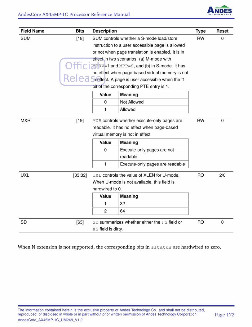
AndesCore AX45MP-1C Processor Reference Manual
Field Name Bits Description Type Reset
SUM [18] SUM controls whether a S-mode load/storeinstruction to a user accessible page is allowedor not when page translation is enabled. It is ineffect in two scenarios: (a) M-mode withMPRV=1 and MPP=S, and (b) in S-mode. It hasno effect when page-based virtual memory is notin effect. A page is user accessible when the Ubit of the corresponding PTE entry is 1.
Value Meaning
0 Not Allowed
1 Allowed
RW 0
MXR [19] MXR controls whether execute-only pages arereadable. It has no effect when page-basedvirtual memory is not in effect.
Value Meaning
0 Execute-only pages are notreadable
1 Execute-only pages are readable
RW 0
UXL [33:32] UXL controls the value of XLEN for U-mode.When U-mode is not available, this field ishardwired to 0.
Value Meaning
1 32
2 64
RO 2/0
SD [63] SD summarizes whether either the FS field orXS field is dirty.
RO 0
When N extension is not supported, the corresponding bits in sstatus are hardwired to zero.
The information contained herein is the exclusive property of Andes Technology Co. and shall not be distributed,reproduced, or disclosed in whole or in part without prior written permission of Andes Technology Corporation.AndesCore_AX45MP-1C_UM248_V1.2
Page 172
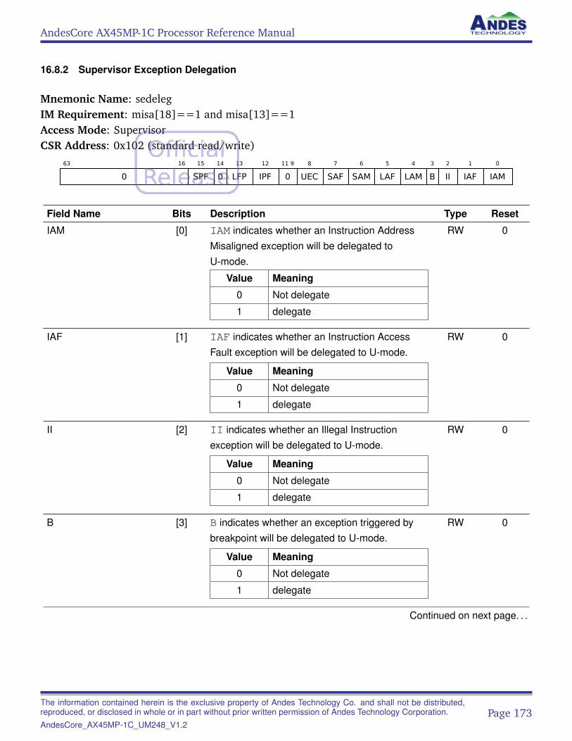
AndesCore AX45MP-1C Processor Reference Manual
16.8.2 Supervisor Exception Delegation
Mnemonic Name: sedelegIM Requirement: misa[18]==1 and misa[13]==1Access Mode: SupervisorCSR Address: 0x102 (standard read/write)
63 16
0
15
SPF
14
0
13
LFP
12
IPF
11 9
0
8
UEC
7
SAF
6
SAM
5
LAF
4
LAM
3
B
2
II
1
IAF
0
IAM
Field Name Bits Description Type Reset
IAM [0] IAM indicates whether an Instruction AddressMisaligned exception will be delegated toU-mode.
Value Meaning
0 Not delegate
1 delegate
RW 0
IAF [1] IAF indicates whether an Instruction AccessFault exception will be delegated to U-mode.
Value Meaning
0 Not delegate
1 delegate
RW 0
II [2] II indicates whether an Illegal Instructionexception will be delegated to U-mode.
Value Meaning
0 Not delegate
1 delegate
RW 0
B [3] B indicates whether an exception triggered bybreakpoint will be delegated to U-mode.
Value Meaning
0 Not delegate
1 delegate
RW 0
Continued on next page. . .
The information contained herein is the exclusive property of Andes Technology Co. and shall not be distributed,reproduced, or disclosed in whole or in part without prior written permission of Andes Technology Corporation.AndesCore_AX45MP-1C_UM248_V1.2
Page 173
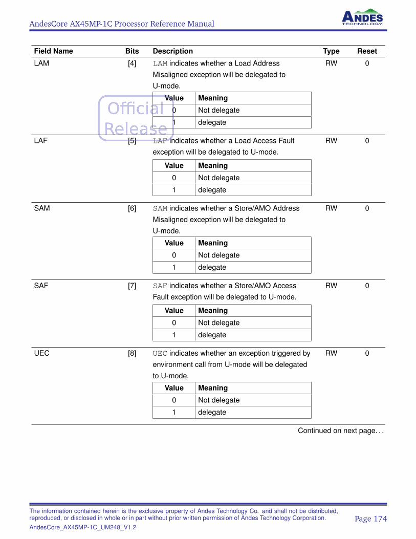
AndesCore AX45MP-1C Processor Reference Manual
Field Name Bits Description Type Reset
LAM [4] LAM indicates whether a Load AddressMisaligned exception will be delegated toU-mode.
Value Meaning
0 Not delegate
1 delegate
RW 0
LAF [5] LAF indicates whether a Load Access Faultexception will be delegated to U-mode.
Value Meaning
0 Not delegate
1 delegate
RW 0
SAM [6] SAM indicates whether a Store/AMO AddressMisaligned exception will be delegated toU-mode.
Value Meaning
0 Not delegate
1 delegate
RW 0
SAF [7] SAF indicates whether a Store/AMO AccessFault exception will be delegated to U-mode.
Value Meaning
0 Not delegate
1 delegate
RW 0
UEC [8] UEC indicates whether an exception triggered byenvironment call from U-mode will be delegatedto U-mode.
Value Meaning
0 Not delegate
1 delegate
RW 0
Continued on next page. . .
The information contained herein is the exclusive property of Andes Technology Co. and shall not be distributed,reproduced, or disclosed in whole or in part without prior written permission of Andes Technology Corporation.AndesCore_AX45MP-1C_UM248_V1.2
Page 174
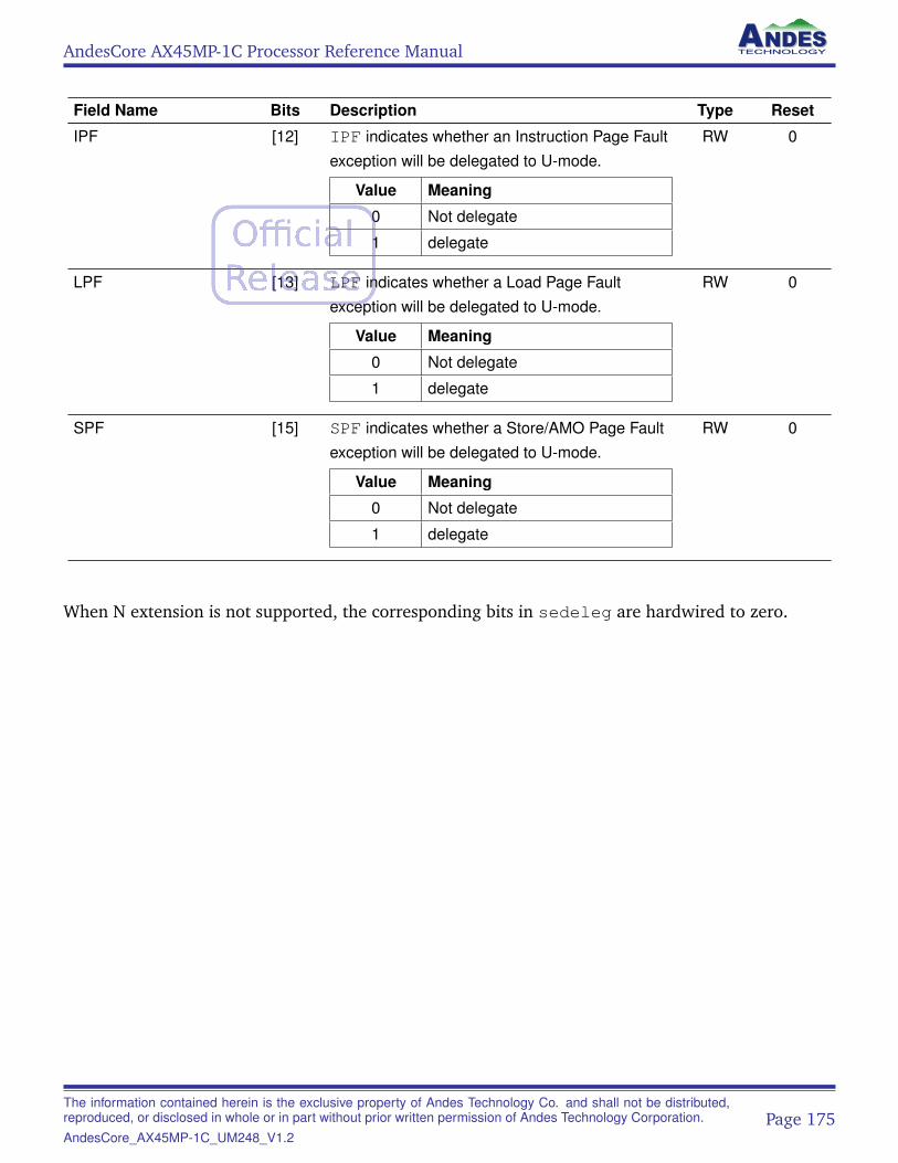
AndesCore AX45MP-1C Processor Reference Manual
Field Name Bits Description Type Reset
IPF [12] IPF indicates whether an Instruction Page Faultexception will be delegated to U-mode.
Value Meaning
0 Not delegate
1 delegate
RW 0
LPF [13] LPF indicates whether a Load Page Faultexception will be delegated to U-mode.
Value Meaning
0 Not delegate
1 delegate
RW 0
SPF [15] SPF indicates whether a Store/AMO Page Faultexception will be delegated to U-mode.
Value Meaning
0 Not delegate
1 delegate
RW 0
When N extension is not supported, the corresponding bits in sedeleg are hardwired to zero.
The information contained herein is the exclusive property of Andes Technology Co. and shall not be distributed,reproduced, or disclosed in whole or in part without prior written permission of Andes Technology Corporation.AndesCore_AX45MP-1C_UM248_V1.2
Page 175
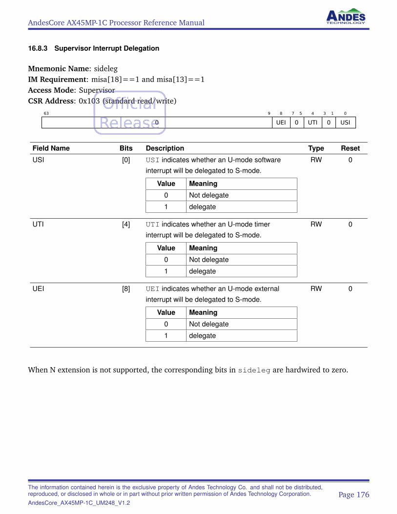
AndesCore AX45MP-1C Processor Reference Manual
16.8.3 Supervisor Interrupt Delegation
Mnemonic Name: sidelegIM Requirement: misa[18]==1 and misa[13]==1Access Mode: SupervisorCSR Address: 0x103 (standard read/write)
63 9
0
8
UEI
7 5
0
4
UTI
3 1
0
0
USI
Field Name Bits Description Type Reset
USI [0] USI indicates whether an U-mode softwareinterrupt will be delegated to S-mode.
Value Meaning
0 Not delegate
1 delegate
RW 0
UTI [4] UTI indicates whether an U-mode timerinterrupt will be delegated to S-mode.
Value Meaning
0 Not delegate
1 delegate
RW 0
UEI [8] UEI indicates whether an U-mode externalinterrupt will be delegated to S-mode.
Value Meaning
0 Not delegate
1 delegate
RW 0
When N extension is not supported, the corresponding bits in sideleg are hardwired to zero.
The information contained herein is the exclusive property of Andes Technology Co. and shall not be distributed,reproduced, or disclosed in whole or in part without prior written permission of Andes Technology Corporation.AndesCore_AX45MP-1C_UM248_V1.2
Page 176
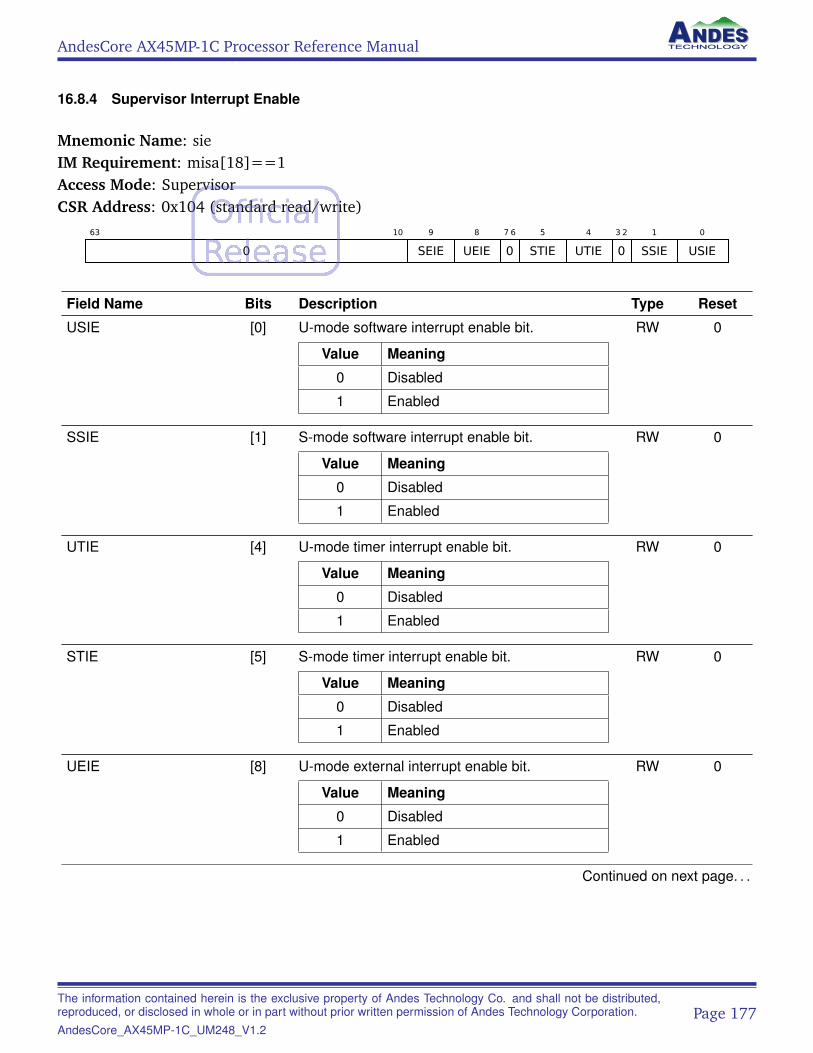
AndesCore AX45MP-1C Processor Reference Manual
16.8.4 Supervisor Interrupt Enable
Mnemonic Name: sieIM Requirement: misa[18]==1Access Mode: SupervisorCSR Address: 0x104 (standard read/write)
63 10
0
9
SEIE
8
UEIE
7 6
0
5
STIE
4
UTIE
3 2
0
1
SSIE
0
USIE
Field Name Bits Description Type Reset
USIE [0] U-mode software interrupt enable bit.
Value Meaning
0 Disabled
1 Enabled
RW 0
SSIE [1] S-mode software interrupt enable bit.
Value Meaning
0 Disabled
1 Enabled
RW 0
UTIE [4] U-mode timer interrupt enable bit.
Value Meaning
0 Disabled
1 Enabled
RW 0
STIE [5] S-mode timer interrupt enable bit.
Value Meaning
0 Disabled
1 Enabled
RW 0
UEIE [8] U-mode external interrupt enable bit.
Value Meaning
0 Disabled
1 Enabled
RW 0
Continued on next page. . .
The information contained herein is the exclusive property of Andes Technology Co. and shall not be distributed,reproduced, or disclosed in whole or in part without prior written permission of Andes Technology Corporation.AndesCore_AX45MP-1C_UM248_V1.2
Page 177
AndesCore AX45MP-1C Processor Reference Manual
Field Name Bits Description Type Reset
SEIE [9] S-mode external interrupt enable bit.
Value Meaning
0 Disabled
1 Enabled
RW 0
When N extension is not supported, the corresponding bits in sie are hardwired to zero.
The information contained herein is the exclusive property of Andes Technology Co. and shall not be distributed,reproduced, or disclosed in whole or in part without prior written permission of Andes Technology Corporation.AndesCore_AX45MP-1C_UM248_V1.2
Page 178
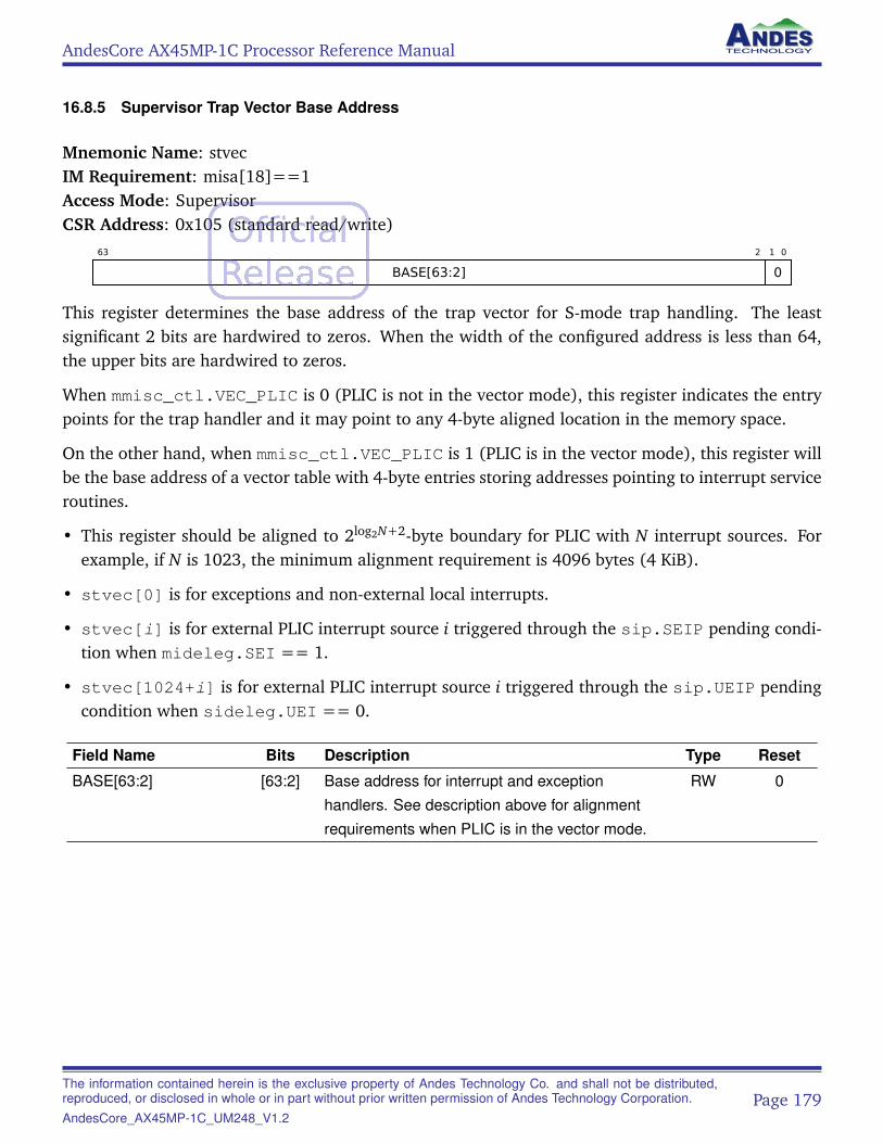
AndesCore AX45MP-1C Processor Reference Manual
16.8.5 Supervisor Trap Vector Base Address
Mnemonic Name: stvecIM Requirement: misa[18]==1Access Mode: SupervisorCSR Address: 0x105 (standard read/write)
63 2
BASE[63:2]
1 0
0
This register determines the base address of the trap vector for S-mode trap handling. The leastsignificant 2 bits are hardwired to zeros. When the width of the configured address is less than 64,the upper bits are hardwired to zeros.
When mmisc_ctl.VEC_PLIC is 0 (PLIC is not in the vector mode), this register indicates the entrypoints for the trap handler and it may point to any 4-byte aligned location in the memory space.
On the other hand, when mmisc_ctl.VEC_PLIC is 1 (PLIC is in the vector mode), this register willbe the base address of a vector table with 4-byte entries storing addresses pointing to interrupt serviceroutines.
• This register should be aligned to 2log2N+2-byte boundary for PLIC with N interrupt sources. Forexample, if N is 1023, the minimum alignment requirement is 4096 bytes (4 KiB).
• stvec[0] is for exceptions and non-external local interrupts.
• stvec[i] is for external PLIC interrupt source i triggered through the sip.SEIP pending condi-tion when mideleg.SEI == 1.
• stvec[1024+i] is for external PLIC interrupt source i triggered through the sip.UEIP pendingcondition when sideleg.UEI == 0.
Field Name Bits Description Type Reset
BASE[63:2] [63:2] Base address for interrupt and exceptionhandlers. See description above for alignmentrequirements when PLIC is in the vector mode.
RW 0
The information contained herein is the exclusive property of Andes Technology Co. and shall not be distributed,reproduced, or disclosed in whole or in part without prior written permission of Andes Technology Corporation.AndesCore_AX45MP-1C_UM248_V1.2
Page 179
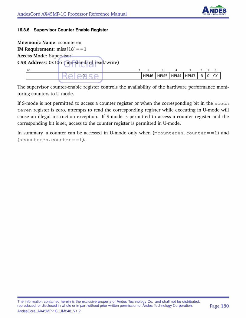
AndesCore AX45MP-1C Processor Reference Manual
16.8.6 Supervisor Counter Enable Register
Mnemonic Name: scounterenIM Requirement: misa[18]==1Access Mode: SupervisorCSR Address: 0x106 (non-standard read/write)
63 7
0
6
HPM6
5
HPM5
4
HPM4
3
HPM3
2
IR
1
0
0
CY
The supervisor counter-enable register controls the availability of the hardware performance moni-toring counters to U-mode.
If S-mode is not permitted to access a counter register or when the corresponding bit in the scoun
teren register is zero, attempts to read the corresponding register while executing in U-mode willcause an illegal instruction exception. If S-mode is permitted to access a counter register and thecorresponding bit is set, access to the counter register is permitted in U-mode.
In summary, a counter can be accessed in U-mode only when (mcounteren.counter==1) and(scounteren.counter==1).
The information contained herein is the exclusive property of Andes Technology Co. and shall not be distributed,reproduced, or disclosed in whole or in part without prior written permission of Andes Technology Corporation.AndesCore_AX45MP-1C_UM248_V1.2
Page 180
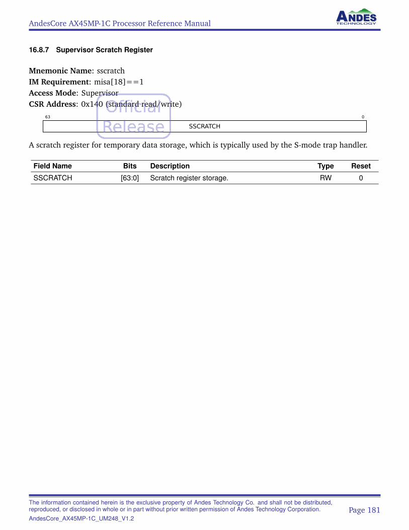
AndesCore AX45MP-1C Processor Reference Manual
16.8.7 Supervisor Scratch Register
Mnemonic Name: sscratchIM Requirement: misa[18]==1Access Mode: SupervisorCSR Address: 0x140 (standard read/write)
63 0
SSCRATCH
A scratch register for temporary data storage, which is typically used by the S-mode trap handler.
Field Name Bits Description Type Reset
SSCRATCH [63:0] Scratch register storage. RW 0
The information contained herein is the exclusive property of Andes Technology Co. and shall not be distributed,reproduced, or disclosed in whole or in part without prior written permission of Andes Technology Corporation.AndesCore_AX45MP-1C_UM248_V1.2
Page 181
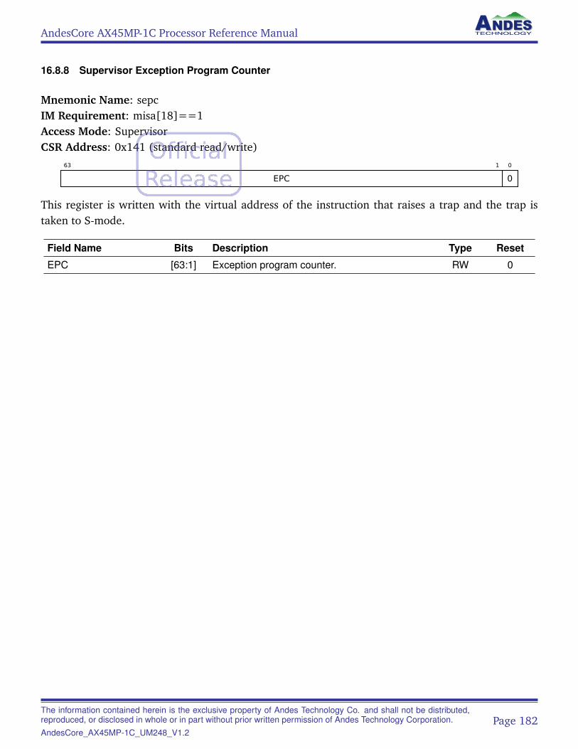
AndesCore AX45MP-1C Processor Reference Manual
16.8.8 Supervisor Exception Program Counter
Mnemonic Name: sepcIM Requirement: misa[18]==1Access Mode: SupervisorCSR Address: 0x141 (standard read/write)
63 1
EPC
0
0
This register is written with the virtual address of the instruction that raises a trap and the trap istaken to S-mode.
Field Name Bits Description Type Reset
EPC [63:1] Exception program counter. RW 0
The information contained herein is the exclusive property of Andes Technology Co. and shall not be distributed,reproduced, or disclosed in whole or in part without prior written permission of Andes Technology Corporation.AndesCore_AX45MP-1C_UM248_V1.2
Page 182
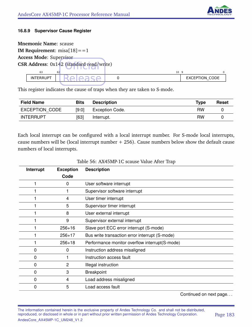
AndesCore AX45MP-1C Processor Reference Manual
16.8.9 Supervisor Cause Register
Mnemonic Name: scauseIM Requirement: misa[18]==1Access Mode: SupervisorCSR Address: 0x142 (standard read/write)
63
INTERRUPT
62 10
0
9 0
EXCEPTION_CODE
This register indicates the cause of traps when they are taken to S-mode.
Field Name Bits Description Type Reset
EXCEPTION_CODE [9:0] Exception Code. RW 0
INTERRUPT [63] Interrupt. RW 0
Each local interrupt can be configured with a local interrupt number. For S-mode local interrupts,cause numbers will be (local interrupt number + 256). Cause numbers below show the default causenumbers of local interrupts.
Table 56: AX45MP-1C scause Value After Trap
Interrupt ExceptionCode
Description
1 0 User software interrupt
1 1 Supervisor software interrupt
1 4 User timer interrupt
1 5 Supervisor timer interrupt
1 8 User external interrupt
1 9 Supervisor external interrupt
1 256+16 Slave port ECC error interrupt (S-mode)
1 256+17 Bus write transaction error interrupt (S-mode)
1 256+18 Performance monitor overflow interrupt(S-mode)
0 0 Instruction address misaligned
0 1 Instruction access fault
0 2 Illegal instruction
0 3 Breakpoint
0 4 Load address misaligned
0 5 Load access fault
Continued on next page. . .
The information contained herein is the exclusive property of Andes Technology Co. and shall not be distributed,reproduced, or disclosed in whole or in part without prior written permission of Andes Technology Corporation.AndesCore_AX45MP-1C_UM248_V1.2
Page 183
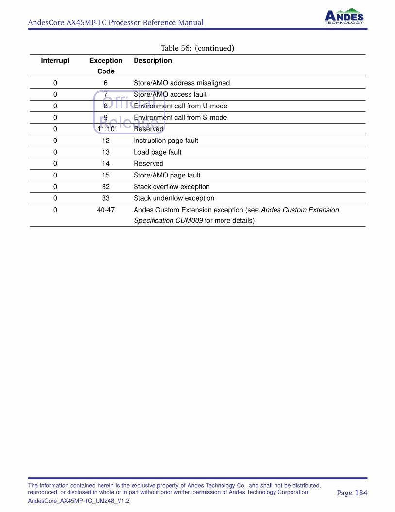
AndesCore AX45MP-1C Processor Reference Manual
Table 56: (continued)
Interrupt ExceptionCode
Description
0 6 Store/AMO address misaligned
0 7 Store/AMO access fault
0 8 Environment call from U-mode
0 9 Environment call from S-mode
0 11:10 Reserved
0 12 Instruction page fault
0 13 Load page fault
0 14 Reserved
0 15 Store/AMO page fault
0 32 Stack overflow exception
0 33 Stack underflow exception
0 40-47 Andes Custom Extension exception (see Andes Custom ExtensionSpecification CUM009 for more details)
The information contained herein is the exclusive property of Andes Technology Co. and shall not be distributed,reproduced, or disclosed in whole or in part without prior written permission of Andes Technology Corporation.AndesCore_AX45MP-1C_UM248_V1.2
Page 184
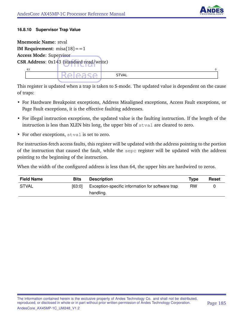
AndesCore AX45MP-1C Processor Reference Manual
16.8.10 Supervisor Trap Value
Mnemonic Name: stvalIM Requirement: misa[18]==1Access Mode: SupervisorCSR Address: 0x143 (standard read/write)
63 0
STVAL
This register is updated when a trap is taken to S-mode. The updated value is dependent on the causeof traps:
• For Hardware Breakpoint exceptions, Address Misaligned exceptions, Access Fault exceptions, orPage Fault exceptions, it is the effective faulting addresses.
• For illegal instruction exceptions, the updated value is the faulting instruction. If the length of theinstruction is less than XLEN bits long, the upper bits of stval are cleared to zero.
• For other exceptions, stval is set to zero.
For instruction-fetch access faults, this register will be updated with the address pointing to the portionof the instruction that caused the fault, while the sepc register will be updated with the addresspointing to the beginning of the instruction.
When the width of the configured address is less than 64, the upper bits are hardwired to zeros.
Field Name Bits Description Type Reset
STVAL [63:0] Exception-specific information for software traphandling.
RW 0
The information contained herein is the exclusive property of Andes Technology Co. and shall not be distributed,reproduced, or disclosed in whole or in part without prior written permission of Andes Technology Corporation.AndesCore_AX45MP-1C_UM248_V1.2
Page 185
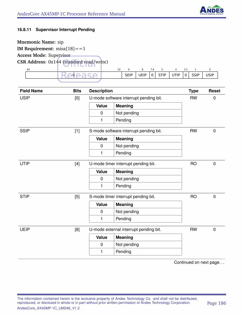
AndesCore AX45MP-1C Processor Reference Manual
16.8.11 Supervisor Interrupt Pending
Mnemonic Name: sipIM Requirement: misa[18]==1Access Mode: SupervisorCSR Address: 0x144 (standard read/write)
63 10
0
9
SEIP
8
UEIP
7 6
0
5
STIP
4
UTIP
3 2
0
1
SSIP
0
USIP
Field Name Bits Description Type Reset
USIP [0] U-mode software interrupt pending bit.
Value Meaning
0 Not pending
1 Pending
RW 0
SSIP [1] S-mode software interrupt pending bit.
Value Meaning
0 Not pending
1 Pending
RW 0
UTIP [4] U-mode timer interrupt pending bit.
Value Meaning
0 Not pending
1 Pending
RO 0
STIP [5] S-mode timer interrupt pending bit.
Value Meaning
0 Not pending
1 Pending
RO 0
UEIP [8] U-mode external interrupt pending bit.
Value Meaning
0 Not pending
1 Pending
RW 0
Continued on next page. . .
The information contained herein is the exclusive property of Andes Technology Co. and shall not be distributed,reproduced, or disclosed in whole or in part without prior written permission of Andes Technology Corporation.AndesCore_AX45MP-1C_UM248_V1.2
Page 186
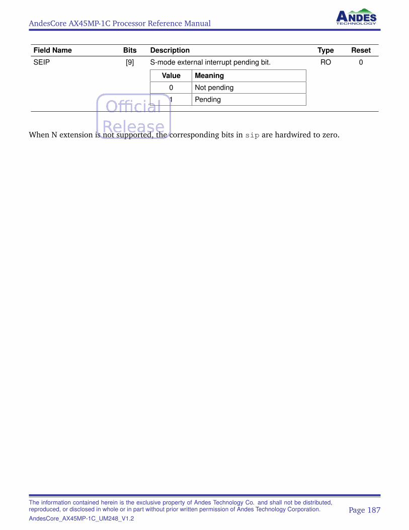
AndesCore AX45MP-1C Processor Reference Manual
Field Name Bits Description Type Reset
SEIP [9] S-mode external interrupt pending bit.
Value Meaning
0 Not pending
1 Pending
RO 0
When N extension is not supported, the corresponding bits in sip are hardwired to zero.
The information contained herein is the exclusive property of Andes Technology Co. and shall not be distributed,reproduced, or disclosed in whole or in part without prior written permission of Andes Technology Corporation.AndesCore_AX45MP-1C_UM248_V1.2
Page 187
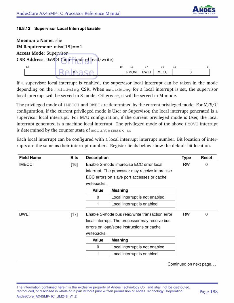
AndesCore AX45MP-1C Processor Reference Manual
16.8.12 Supervisor Local Interrupt Enable
Mnemonic Name: slieIM Requirement: misa[18]==1Access Mode: SupervisorCSR Address: 0x9C4 (non-standard read/write)
63 19
0
18
PMOVI
17
BWEI
16
IMECCI
15 0
0
If a supervisor local interrupt is enabled, the supervisor local interrupt can be taken in the modedepending on the mslideleg CSR. When mslideleg for a local interrupt is set, the supervisorlocal interrupt will be served in S-mode. Otherwise, it will be served in M-mode.
The privileged mode of IMECCI and BWEI are determined by the current privileged mode. For M/S/Uconfiguration, if the current privileged mode is User or Supervisor, the local interrupt generated is asupervisor local interrupt. For M/U configuration, if the current privileged mode is User, the localinterrupt generated is a machine local interrupt. The privileged mode of the above PMOVI interruptis determined by the counter state of mcountermask_m.
Each local interrupt can be configured with a local interrupt interrupt number. Bit location of inter-rupts are the same as their interrupt numbers. Register fields below show the default bit location.
Field Name Bits Description Type Reset
IMECCI [16] Enable S-mode imprecise ECC error localinterrupt. The processor may receive impreciseECC errors on slave port accesses or cachewritebacks.
Value Meaning
0 Local interrupt is not enabled.
1 Local interrupt is enabled.
RW 0
BWEI [17] Enable S-mode bus read/write transaction errorlocal interrupt. The processor may receive buserrors on load/store instructions or cachewritebacks.
Value Meaning
0 Local interrupt is not enabled.
1 Local interrupt is enabled.
RW 0
Continued on next page. . .
The information contained herein is the exclusive property of Andes Technology Co. and shall not be distributed,reproduced, or disclosed in whole or in part without prior written permission of Andes Technology Corporation.AndesCore_AX45MP-1C_UM248_V1.2
Page 188
AndesCore AX45MP-1C Processor Reference Manual
Field Name Bits Description Type Reset
PMOVI [18] Enable S-mode performance monitor overflowlocal interrupt.
Value Meaning
0 Local interrupt is not enabled.
1 Local interrupt is enabled.
RW 0
The information contained herein is the exclusive property of Andes Technology Co. and shall not be distributed,reproduced, or disclosed in whole or in part without prior written permission of Andes Technology Corporation.AndesCore_AX45MP-1C_UM248_V1.2
Page 189
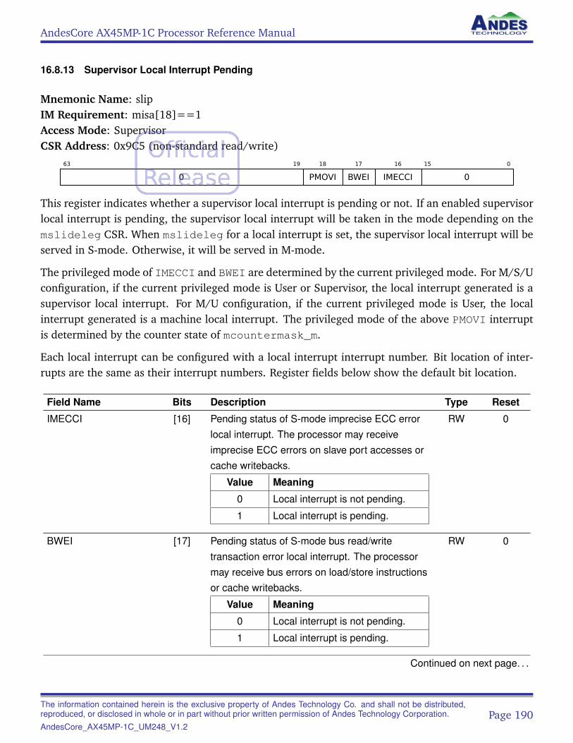
AndesCore AX45MP-1C Processor Reference Manual
16.8.13 Supervisor Local Interrupt Pending
Mnemonic Name: slipIM Requirement: misa[18]==1Access Mode: SupervisorCSR Address: 0x9C5 (non-standard read/write)
63 19
0
18
PMOVI
17
BWEI
16
IMECCI
15 0
0
This register indicates whether a supervisor local interrupt is pending or not. If an enabled supervisorlocal interrupt is pending, the supervisor local interrupt will be taken in the mode depending on themslideleg CSR. When mslideleg for a local interrupt is set, the supervisor local interrupt will beserved in S-mode. Otherwise, it will be served in M-mode.
The privileged mode of IMECCI and BWEI are determined by the current privileged mode. For M/S/Uconfiguration, if the current privileged mode is User or Supervisor, the local interrupt generated is asupervisor local interrupt. For M/U configuration, if the current privileged mode is User, the localinterrupt generated is a machine local interrupt. The privileged mode of the above PMOVI interruptis determined by the counter state of mcountermask_m.
Each local interrupt can be configured with a local interrupt interrupt number. Bit location of inter-rupts are the same as their interrupt numbers. Register fields below show the default bit location.
Field Name Bits Description Type Reset
IMECCI [16] Pending status of S-mode imprecise ECC errorlocal interrupt. The processor may receiveimprecise ECC errors on slave port accesses orcache writebacks.
Value Meaning
0 Local interrupt is not pending.
1 Local interrupt is pending.
RW 0
BWEI [17] Pending status of S-mode bus read/writetransaction error local interrupt. The processormay receive bus errors on load/store instructionsor cache writebacks.
Value Meaning
0 Local interrupt is not pending.
1 Local interrupt is pending.
RW 0
Continued on next page. . .
The information contained herein is the exclusive property of Andes Technology Co. and shall not be distributed,reproduced, or disclosed in whole or in part without prior written permission of Andes Technology Corporation.AndesCore_AX45MP-1C_UM248_V1.2
Page 190
AndesCore AX45MP-1C Processor Reference Manual
Field Name Bits Description Type Reset
PMOVI [18] Pending status of S-mode performance monitoroverflow local interrupt.
Value Meaning
0 Local interrupt is not pending.
1 Local interrupt is pending.
RW 0
The information contained herein is the exclusive property of Andes Technology Co. and shall not be distributed,reproduced, or disclosed in whole or in part without prior written permission of Andes Technology Corporation.AndesCore_AX45MP-1C_UM248_V1.2
Page 191
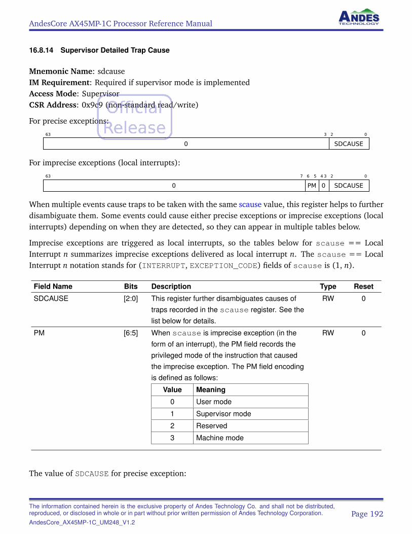
AndesCore AX45MP-1C Processor Reference Manual
16.8.14 Supervisor Detailed Trap Cause
Mnemonic Name: sdcauseIM Requirement: Required if supervisor mode is implementedAccess Mode: SupervisorCSR Address: 0x9c9 (non-standard read/write)
For precise exceptions:
63 3
0
2 0
SDCAUSE
For imprecise exceptions (local interrupts):
63 7
0
6 5
PM
4 3
0
2 0
SDCAUSE
When multiple events cause traps to be taken with the same scause value, this register helps to furtherdisambiguate them. Some events could cause either precise exceptions or imprecise exceptions (localinterrupts) depending on when they are detected, so they can appear in multiple tables below.
Imprecise exceptions are triggered as local interrupts, so the tables below for scause == LocalInterrupt n summarizes imprecise exceptions delivered as local interrupt n. The scause == LocalInterrupt n notation stands for (INTERRUPT, EXCEPTION_CODE) fields of scause is (1, n).
Field Name Bits Description Type Reset
SDCAUSE [2:0] This register further disambiguates causes oftraps recorded in the scause register. See thelist below for details.
RW 0
PM [6:5] When scause is imprecise exception (in theform of an interrupt), the PM field records theprivileged mode of the instruction that causedthe imprecise exception. The PM field encodingis defined as follows:
Value Meaning
0 User mode
1 Supervisor mode
2 Reserved
3 Machine mode
RW 0
The value of SDCAUSE for precise exception:
The information contained herein is the exclusive property of Andes Technology Co. and shall not be distributed,reproduced, or disclosed in whole or in part without prior written permission of Andes Technology Corporation.AndesCore_AX45MP-1C_UM248_V1.2
Page 192
AndesCore AX45MP-1C Processor Reference Manual
• When scause == 1 (Instruction access fault)
Value Meaning
0 Reserved
1 ECC/Parity error
2 PMP instruction access violation
3 Bus error
4 PMA empty hole access
• When scause == 2 (Illegal instruction)
Value Meaning
0 Please parse the stval CSR
1 FP disabled exception
2 Reserved
• When scause == 5 (Load access fault)
Value Meaning
0 Reserved
1 ECC/Parity error
2 PMP load access violation
3 Bus error
4 Misaligned address
5 PMA empty hole access
6 PMA attribute inconsistency
7 PMA NAMO exception
• When scause == 7 (Store access fault)
Value Meaning
0 Reserved
1 ECC/Parity error
2 PMP store access violation
3 Bus error
4 Misaligned address
Continued on next page. . .
The information contained herein is the exclusive property of Andes Technology Co. and shall not be distributed,reproduced, or disclosed in whole or in part without prior written permission of Andes Technology Corporation.AndesCore_AX45MP-1C_UM248_V1.2
Page 193
AndesCore AX45MP-1C Processor Reference Manual
Value Meaning
5 PMA empty hole access
6 PMA attribute inconsistency
7 PMA NAMO exception
The value of SDCAUSE for imprecise exception:
• When scause == Local Interrupt 272 (16 + 256) (ECC error local interrupt)
Value Meaning
0 Reserved
1 LM slave port ECC/Parity error
2 Imprecise store ECC/Parity error
3 Imprecise load ECC/Parity error
• When scause == Local Interrupt 273 (17 + 256) (Bus read/write transaction error local inter-rupt)
Value Meaning
0 Reserved
1 Bus read error
2 Bus write error
3 PMP error caused by loadinstructions
4 PMP error caused by storeinstructions
5 PMA error caused by loadinstructions"
6 PMA error caused by storeinstructions
• For PMOVI, SDCAUSE will be written 0. For other exceptions and interrupts, this register will notbe updated.
The information contained herein is the exclusive property of Andes Technology Co. and shall not be distributed,reproduced, or disclosed in whole or in part without prior written permission of Andes Technology Corporation.AndesCore_AX45MP-1C_UM248_V1.2
Page 194
AndesCore AX45MP-1C Processor Reference Manual
16.8.14.1 Detailed Exception Priority
Within Instruction/Load/Store access fault exceptions, the priority of a PMP exception is higher thanthe priority of a PMA exception, when both types of exceptions happen on the same instruction.
The information contained herein is the exclusive property of Andes Technology Co. and shall not be distributed,reproduced, or disclosed in whole or in part without prior written permission of Andes Technology Corporation.AndesCore_AX45MP-1C_UM248_V1.2
Page 195
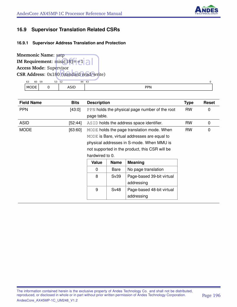
AndesCore AX45MP-1C Processor Reference Manual
16.9 Supervisor Translation Related CSRs
16.9.1 Supervisor Address Translation and Protection
Mnemonic Name: satpIM Requirement: misa[18]==1Access Mode: SupervisorCSR Address: 0x180 (standard read/write)
63 60
MODE
59 53
0
52 44
ASID
43 0
PPN
Field Name Bits Description Type Reset
PPN [43:0] PPN holds the physical page number of the rootpage table.
RW 0
ASID [52:44] ASID holds the address space identifier. RW 0
MODE [63:60] MODE holds the page translation mode. WhenMODE is Bare, virtual addresses are equal tophysical addresses in S-mode. When MMU isnot supported in the product, this CSR will behardwired to 0.
Value Name Meaning
0 Bare No page translation
8 Sv39 Page-based 39-bit virtualaddressing
9 Sv48 Page-based 48-bit virtualaddressing
RW 0
The information contained herein is the exclusive property of Andes Technology Co. and shall not be distributed,reproduced, or disclosed in whole or in part without prior written permission of Andes Technology Corporation.AndesCore_AX45MP-1C_UM248_V1.2
Page 196
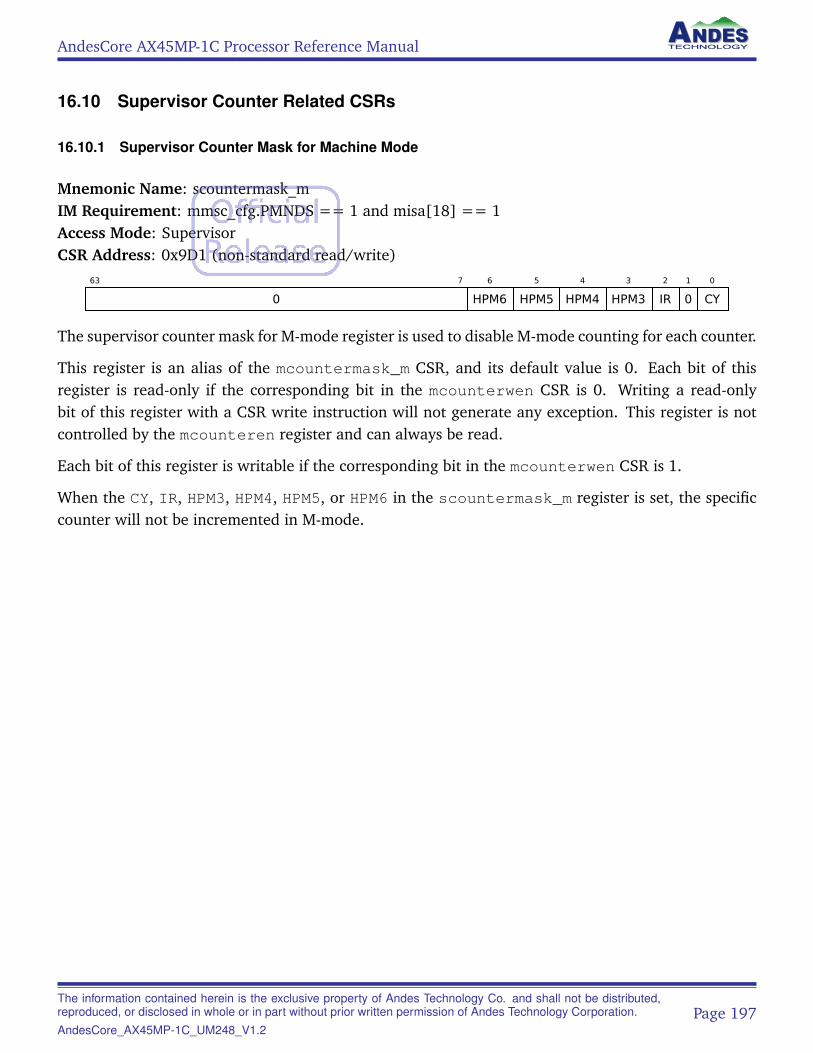
AndesCore AX45MP-1C Processor Reference Manual
16.10 Supervisor Counter Related CSRs
16.10.1 Supervisor Counter Mask for Machine Mode
Mnemonic Name: scountermask_mIM Requirement: mmsc_cfg.PMNDS == 1 and misa[18] == 1Access Mode: SupervisorCSR Address: 0x9D1 (non-standard read/write)
63 7
0
6
HPM6
5
HPM5
4
HPM4
3
HPM3
2
IR
1
0
0
CY
The supervisor counter mask for M-mode register is used to disable M-mode counting for each counter.
This register is an alias of the mcountermask_m CSR, and its default value is 0. Each bit of thisregister is read-only if the corresponding bit in the mcounterwen CSR is 0. Writing a read-onlybit of this register with a CSR write instruction will not generate any exception. This register is notcontrolled by the mcounteren register and can always be read.
Each bit of this register is writable if the corresponding bit in the mcounterwen CSR is 1.
When the CY, IR, HPM3, HPM4, HPM5, or HPM6 in the scountermask_m register is set, the specificcounter will not be incremented in M-mode.
The information contained herein is the exclusive property of Andes Technology Co. and shall not be distributed,reproduced, or disclosed in whole or in part without prior written permission of Andes Technology Corporation.AndesCore_AX45MP-1C_UM248_V1.2
Page 197

AndesCore AX45MP-1C Processor Reference Manual
16.10.2 Supervisor Counter Mask for Supervisor Mode
Mnemonic Name: scountermask_sIM Requirement: mmsc_cfg.PMNDS == 1 and misa[18] == 1Access Mode: SupervisorCSR Address: 0x9D2 (non-standard read/write)
63 7
0
6
HPM6
5
HPM5
4
HPM4
3
HPM3
2
IR
1
0
0
CY
The supervisor counter mask for S-mode register controls the performance counter behavior in S-mode. The default value of this register is 0.
This register is an alias of the mcountermask_s CSR, and its default value is 0. Each bit of thisregister is read-only if the corresponding bit in the mcounterwen CSR is 0. Writing a read-onlybit of this register with a CSR write instruction will not generate any exception. This register is notcontrolled by the mcounteren register and can always be read.
Each bit of this register is writable if the corresponding bit in the mcounterwen CSR is 1.
When the CY, IR, HPM3, HPM4, HPM5, or HPM6 in the scountermask_s register is set, the specificcounter will not be incremented in S-mode.
The information contained herein is the exclusive property of Andes Technology Co. and shall not be distributed,reproduced, or disclosed in whole or in part without prior written permission of Andes Technology Corporation.AndesCore_AX45MP-1C_UM248_V1.2
Page 198
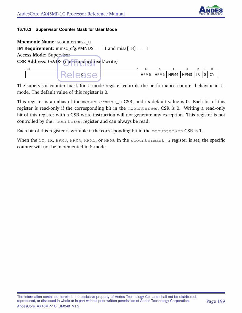
AndesCore AX45MP-1C Processor Reference Manual
16.10.3 Supervisor Counter Mask for User Mode
Mnemonic Name: scountermask_uIM Requirement: mmsc_cfg.PMNDS == 1 and misa[18] == 1Access Mode: SupervisorCSR Address: 0x9D3 (non-standard read/write)
63 7
0
6
HPM6
5
HPM5
4
HPM4
3
HPM3
2
IR
1
0
0
CY
The supervisor counter mask for U-mode register controls the performance counter behavior in U-mode. The default value of this register is 0.
This register is an alias of the mcountermask_u CSR, and its default value is 0. Each bit of thisregister is read-only if the corresponding bit in the mcounterwen CSR is 0. Writing a read-onlybit of this register with a CSR write instruction will not generate any exception. This register is notcontrolled by the mcounteren register and can always be read.
Each bit of this register is writable if the corresponding bit in the mcounterwen CSR is 1.
When the CY, IR, HPM3, HPM4, HPM5, or HPM6 in the scountermask_u register is set, the specificcounter will not be incremented in S-mode.
The information contained herein is the exclusive property of Andes Technology Co. and shall not be distributed,reproduced, or disclosed in whole or in part without prior written permission of Andes Technology Corporation.AndesCore_AX45MP-1C_UM248_V1.2
Page 199
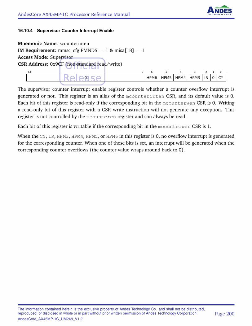
AndesCore AX45MP-1C Processor Reference Manual
16.10.4 Supervisor Counter Interrupt Enable
Mnemonic Name: scounterintenIM Requirement: mmsc_cfg.PMNDS==1 & misa[18]==1Access Mode: SupervisorCSR Address: 0x9CF (non-standard read/write)
63 7
0
6
HPM6
5
HPM5
4
HPM4
3
HPM3
2
IR
1
0
0
CY
The supervisor counter interrupt enable register controls whether a counter overflow interrupt isgenerated or not. This register is an alias of the mcounterinten CSR, and its default value is 0.Each bit of this register is read-only if the corresponding bit in the mcounterwen CSR is 0. Writinga read-only bit of this register with a CSR write instruction will not generate any exception. Thisregister is not controlled by the mcounteren register and can always be read.
Each bit of this register is writable if the corresponding bit in the mcounterwen CSR is 1.
When the CY, IR, HPM3, HPM4, HPM5, or HPM6 in this register is 0, no overflow interrupt is generatedfor the corresponding counter. When one of these bits is set, an interrupt will be generated when thecorresponding counter overflows (the counter value wraps around back to 0).
The information contained herein is the exclusive property of Andes Technology Co. and shall not be distributed,reproduced, or disclosed in whole or in part without prior written permission of Andes Technology Corporation.AndesCore_AX45MP-1C_UM248_V1.2
Page 200
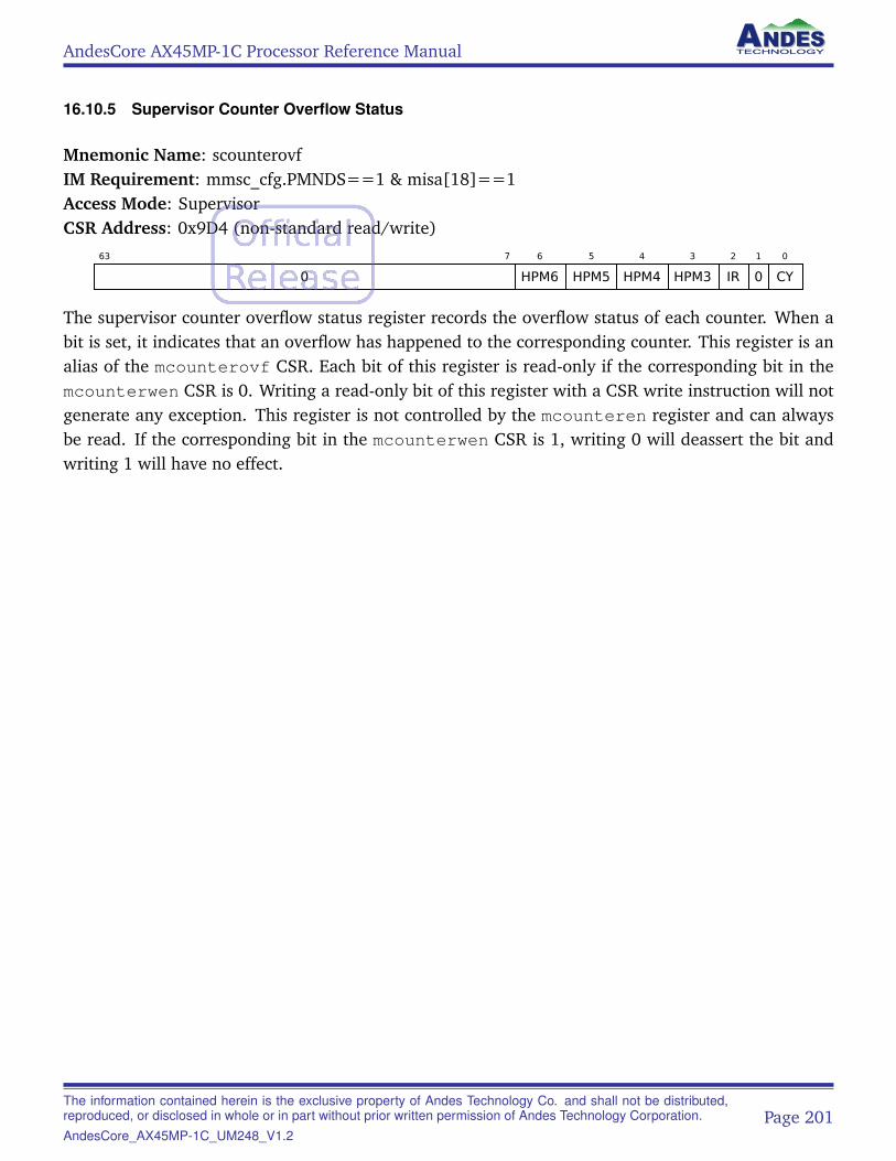
AndesCore AX45MP-1C Processor Reference Manual
16.10.5 Supervisor Counter Overflow Status
Mnemonic Name: scounterovfIM Requirement: mmsc_cfg.PMNDS==1 & misa[18]==1Access Mode: SupervisorCSR Address: 0x9D4 (non-standard read/write)
63 7
0
6
HPM6
5
HPM5
4
HPM4
3
HPM3
2
IR
1
0
0
CY
The supervisor counter overflow status register records the overflow status of each counter. When abit is set, it indicates that an overflow has happened to the corresponding counter. This register is analias of the mcounterovf CSR. Each bit of this register is read-only if the corresponding bit in themcounterwen CSR is 0. Writing a read-only bit of this register with a CSR write instruction will notgenerate any exception. This register is not controlled by the mcounteren register and can alwaysbe read. If the corresponding bit in the mcounterwen CSR is 1, writing 0 will deassert the bit andwriting 1 will have no effect.
The information contained herein is the exclusive property of Andes Technology Co. and shall not be distributed,reproduced, or disclosed in whole or in part without prior written permission of Andes Technology Corporation.AndesCore_AX45MP-1C_UM248_V1.2
Page 201
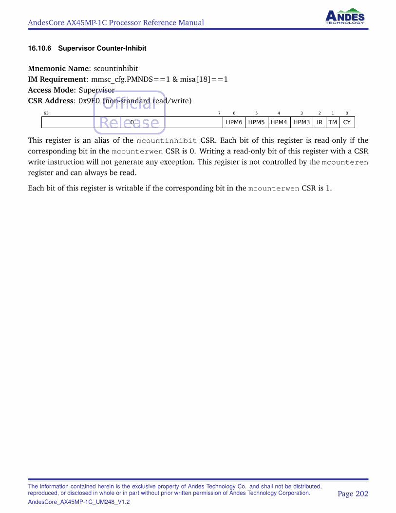
AndesCore AX45MP-1C Processor Reference Manual
16.10.6 Supervisor Counter-Inhibit
Mnemonic Name: scountinhibitIM Requirement: mmsc_cfg.PMNDS==1 & misa[18]==1Access Mode: SupervisorCSR Address: 0x9E0 (non-standard read/write)
63 7
0
6
HPM6
5
HPM5
4
HPM4
3
HPM3
2
IR
1
TM
0
CY
This register is an alias of the mcountinhibit CSR. Each bit of this register is read-only if thecorresponding bit in the mcounterwen CSR is 0. Writing a read-only bit of this register with a CSRwrite instruction will not generate any exception. This register is not controlled by the mcounterenregister and can always be read.
Each bit of this register is writable if the corresponding bit in the mcounterwen CSR is 1.
The information contained herein is the exclusive property of Andes Technology Co. and shall not be distributed,reproduced, or disclosed in whole or in part without prior written permission of Andes Technology Corporation.AndesCore_AX45MP-1C_UM248_V1.2
Page 202
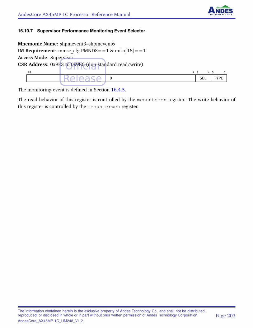
AndesCore AX45MP-1C Processor Reference Manual
16.10.7 Supervisor Performance Monitoring Event Selector
Mnemonic Name: shpmevent3–shpmevent6IM Requirement: mmsc_cfg.PMNDS==1 & misa[18]==1Access Mode: SupervisorCSR Address: 0x9E3 to 0x9E6 (non-standard read/write)
63 9
0
8 4
SEL
3 0
TYPE
The monitoring event is defined in Section 16.4.5.
The read behavior of this register is controlled by the mcounteren register. The write behavior ofthis register is controlled by the mcounterwen register.
The information contained herein is the exclusive property of Andes Technology Co. and shall not be distributed,reproduced, or disclosed in whole or in part without prior written permission of Andes Technology Corporation.AndesCore_AX45MP-1C_UM248_V1.2
Page 203
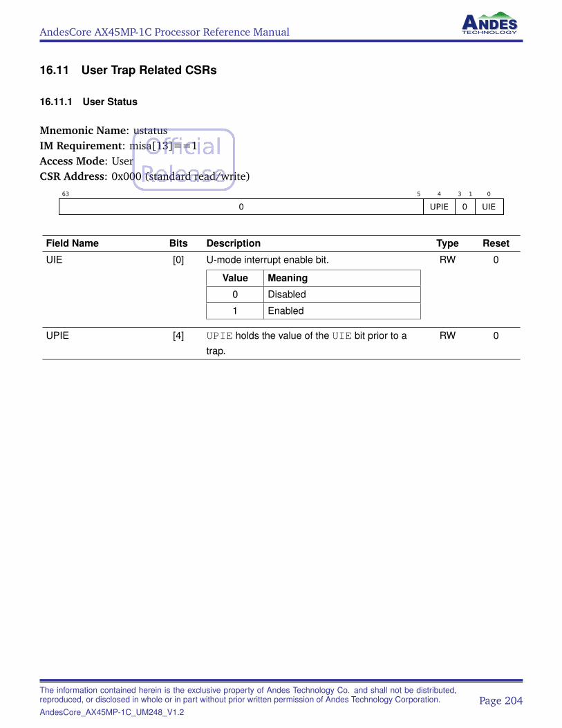
AndesCore AX45MP-1C Processor Reference Manual
16.11 User Trap Related CSRs
16.11.1 User Status
Mnemonic Name: ustatusIM Requirement: misa[13]==1Access Mode: UserCSR Address: 0x000 (standard read/write)
63 5
0
4
UPIE
3 1
0
0
UIE
Field Name Bits Description Type Reset
UIE [0] U-mode interrupt enable bit.
Value Meaning
0 Disabled
1 Enabled
RW 0
UPIE [4] UPIE holds the value of the UIE bit prior to atrap.
RW 0
The information contained herein is the exclusive property of Andes Technology Co. and shall not be distributed,reproduced, or disclosed in whole or in part without prior written permission of Andes Technology Corporation.AndesCore_AX45MP-1C_UM248_V1.2
Page 204
AndesCore AX45MP-1C Processor Reference Manual
16.11.2 User Interrupt Enable
Mnemonic Name: uieIM Requirement: misa[13]==1Access Mode: UserCSR Address: 0x004 (standard read/write)
63 9
0
8
UEIE
7 5
0
4
UTIE
3 1
0
0
USIE
Field Name Bits Description Type Reset
USIE [0] U-mode software interrupt enable bit.
Value Meaning
0 Disabled
1 Enabled
RW 0
UTIE [4] U-mode timer interrupt enable bit.
Value Meaning
0 Disabled
1 Enabled
RW 0
UEIE [8] U-mode external interrupt enable bit.
Value Meaning
0 Disabled
1 Enabled
RW 0
The information contained herein is the exclusive property of Andes Technology Co. and shall not be distributed,reproduced, or disclosed in whole or in part without prior written permission of Andes Technology Corporation.AndesCore_AX45MP-1C_UM248_V1.2
Page 205
AndesCore AX45MP-1C Processor Reference Manual
16.11.3 User Trap Vector Base Address
Mnemonic Name: utvecIM Requirement: misa[13]==1Access Mode: UserCSR Address: 0x005 (standard read/write)
63 2
BASE[63:2]
1 0
0
This register determines the base address of the trap vector for U-mode trap handling. The leastsignificant 2 bits are hardwired to zeros. When the width of the configured address is less than 64,the upper bits are hardwired to zeros.
When mmisc_ctl.VEC_PLIC is 0 (PLIC is not in the vector mode), this register indicates the entrypoints for the trap handler and it may point to any 4-byte aligned location in the memory space.
On the other hand, when mmisc_ctl.VEC_PLIC is 1 (PLIC is in the vector mode), this register willbe the base address of a vector table with 4-byte entries storing addresses pointing to interrupt serviceroutines. And this register should be aligned to 2log2N+2-byte boundary for PLIC with N interruptsources. For example, if N is 1023, the minimum alignment requirement is 4096 bytes (4 KiB).
Field Name Bits Description Type Reset
BASE[63:2] [63:2] Base address for interrupt and exceptionhandlers. See description above for alignmentrequirements when PLIC is in the vector mode.
RW 0
The information contained herein is the exclusive property of Andes Technology Co. and shall not be distributed,reproduced, or disclosed in whole or in part without prior written permission of Andes Technology Corporation.AndesCore_AX45MP-1C_UM248_V1.2
Page 206
AndesCore AX45MP-1C Processor Reference Manual
16.11.4 User Scratch Register
Mnemonic Name: uscratchIM Requirement: misa[13]==1Access Mode: UserCSR Address: 0x040 (standard read/write)
63 0
USCRATCH
A scratch register for temporary data storage, which is typically used by the U-mode trap handler.
Field Name Bits Description Type Reset
USCRATCH [63:0] Scratch register storage. RW 0
The information contained herein is the exclusive property of Andes Technology Co. and shall not be distributed,reproduced, or disclosed in whole or in part without prior written permission of Andes Technology Corporation.AndesCore_AX45MP-1C_UM248_V1.2
Page 207
AndesCore AX45MP-1C Processor Reference Manual
16.11.5 User Exception Program Counter
Mnemonic Name: uepcIM Requirement: misa[13]==1Access Mode: UserCSR Address: 0x041 (standard read/write)
63 1
EPC
0
0
This register is written with the virtual address of the instruction that raises a trap and the trap istaken to U-mode.
Field Name Bits Description Type Reset
EPC [63:1] Exception program counter. RW 0
The information contained herein is the exclusive property of Andes Technology Co. and shall not be distributed,reproduced, or disclosed in whole or in part without prior written permission of Andes Technology Corporation.AndesCore_AX45MP-1C_UM248_V1.2
Page 208
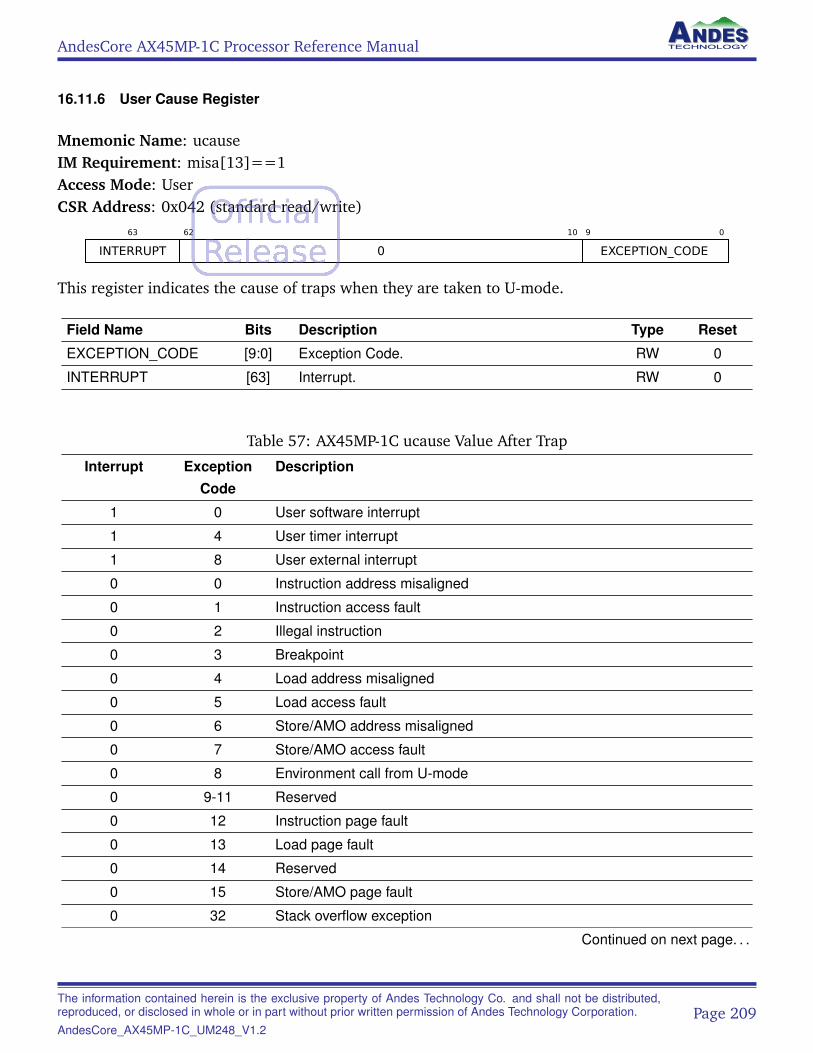
AndesCore AX45MP-1C Processor Reference Manual
16.11.6 User Cause Register
Mnemonic Name: ucauseIM Requirement: misa[13]==1Access Mode: UserCSR Address: 0x042 (standard read/write)
63
INTERRUPT
62 10
0
9 0
EXCEPTION_CODE
This register indicates the cause of traps when they are taken to U-mode.
Field Name Bits Description Type Reset
EXCEPTION_CODE [9:0] Exception Code. RW 0
INTERRUPT [63] Interrupt. RW 0
Table 57: AX45MP-1C ucause Value After Trap
Interrupt ExceptionCode
Description
1 0 User software interrupt
1 4 User timer interrupt
1 8 User external interrupt
0 0 Instruction address misaligned
0 1 Instruction access fault
0 2 Illegal instruction
0 3 Breakpoint
0 4 Load address misaligned
0 5 Load access fault
0 6 Store/AMO address misaligned
0 7 Store/AMO access fault
0 8 Environment call from U-mode
0 9-11 Reserved
0 12 Instruction page fault
0 13 Load page fault
0 14 Reserved
0 15 Store/AMO page fault
0 32 Stack overflow exception
Continued on next page. . .
The information contained herein is the exclusive property of Andes Technology Co. and shall not be distributed,reproduced, or disclosed in whole or in part without prior written permission of Andes Technology Corporation.AndesCore_AX45MP-1C_UM248_V1.2
Page 209
AndesCore AX45MP-1C Processor Reference Manual
Table 57: (continued)
Interrupt ExceptionCode
Description
0 33 Stack underflow exception
0 40-47 Andes Custom Extension exception (see Andes Custom ExtensionSpecification CUM009 for more details)
The information contained herein is the exclusive property of Andes Technology Co. and shall not be distributed,reproduced, or disclosed in whole or in part without prior written permission of Andes Technology Corporation.AndesCore_AX45MP-1C_UM248_V1.2
Page 210
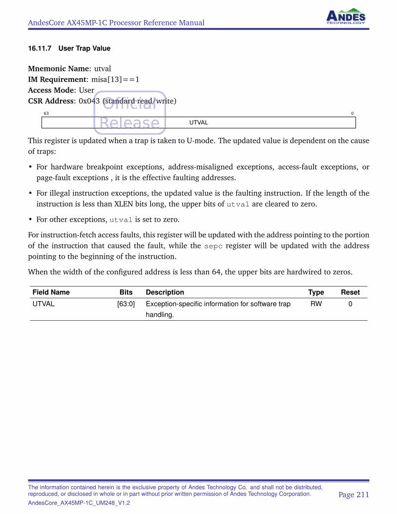
AndesCore AX45MP-1C Processor Reference Manual
16.11.7 User Trap Value
Mnemonic Name: utvalIM Requirement: misa[13]==1Access Mode: UserCSR Address: 0x043 (standard read/write)
63 0
UTVAL
This register is updated when a trap is taken to U-mode. The updated value is dependent on the causeof traps:
• For hardware breakpoint exceptions, address-misaligned exceptions, access-fault exceptions, orpage-fault exceptions , it is the effective faulting addresses.
• For illegal instruction exceptions, the updated value is the faulting instruction. If the length of theinstruction is less than XLEN bits long, the upper bits of utval are cleared to zero.
• For other exceptions, utval is set to zero.
For instruction-fetch access faults, this register will be updated with the address pointing to the portionof the instruction that caused the fault, while the sepc register will be updated with the addresspointing to the beginning of the instruction.
When the width of the configured address is less than 64, the upper bits are hardwired to zeros.
Field Name Bits Description Type Reset
UTVAL [63:0] Exception-specific information for software traphandling.
RW 0
The information contained herein is the exclusive property of Andes Technology Co. and shall not be distributed,reproduced, or disclosed in whole or in part without prior written permission of Andes Technology Corporation.AndesCore_AX45MP-1C_UM248_V1.2
Page 211
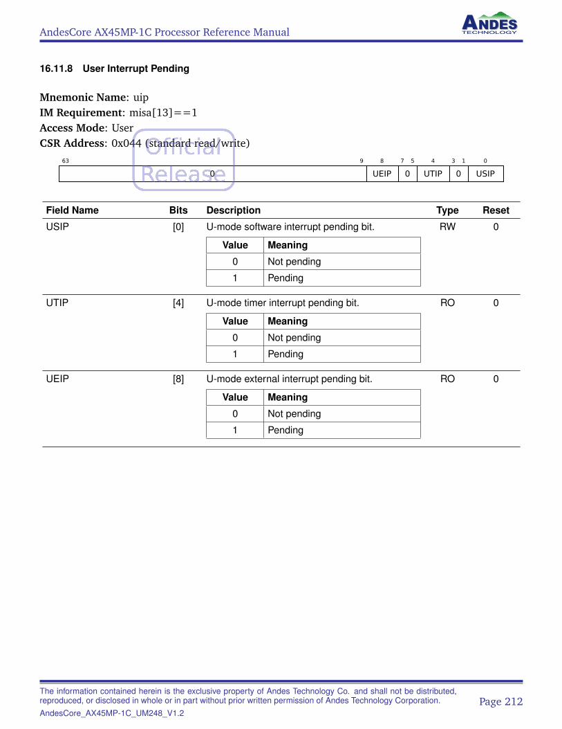
AndesCore AX45MP-1C Processor Reference Manual
16.11.8 User Interrupt Pending
Mnemonic Name: uipIM Requirement: misa[13]==1Access Mode: UserCSR Address: 0x044 (standard read/write)
63 9
0
8
UEIP
7 5
0
4
UTIP
3 1
0
0
USIP
Field Name Bits Description Type Reset
USIP [0] U-mode software interrupt pending bit.
Value Meaning
0 Not pending
1 Pending
RW 0
UTIP [4] U-mode timer interrupt pending bit.
Value Meaning
0 Not pending
1 Pending
RO 0
UEIP [8] U-mode external interrupt pending bit.
Value Meaning
0 Not pending
1 Pending
RO 0
The information contained herein is the exclusive property of Andes Technology Co. and shall not be distributed,reproduced, or disclosed in whole or in part without prior written permission of Andes Technology Corporation.AndesCore_AX45MP-1C_UM248_V1.2
Page 212
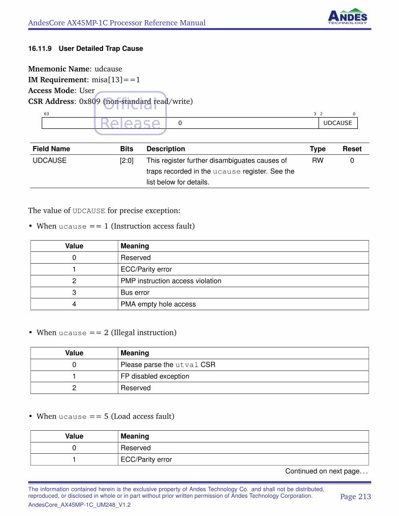
AndesCore AX45MP-1C Processor Reference Manual
16.11.9 User Detailed Trap Cause
Mnemonic Name: udcauseIM Requirement: misa[13]==1Access Mode: UserCSR Address: 0x809 (non-standard read/write)
63 3
0
2 0
UDCAUSE
Field Name Bits Description Type Reset
UDCAUSE [2:0] This register further disambiguates causes oftraps recorded in the ucause register. See thelist below for details.
RW 0
The value of UDCAUSE for precise exception:
• When ucause == 1 (Instruction access fault)
Value Meaning
0 Reserved
1 ECC/Parity error
2 PMP instruction access violation
3 Bus error
4 PMA empty hole access
• When ucause == 2 (Illegal instruction)
Value Meaning
0 Please parse the utval CSR
1 FP disabled exception
2 Reserved
• When ucause == 5 (Load access fault)
Value Meaning
0 Reserved
1 ECC/Parity error
Continued on next page. . .
The information contained herein is the exclusive property of Andes Technology Co. and shall not be distributed,reproduced, or disclosed in whole or in part without prior written permission of Andes Technology Corporation.AndesCore_AX45MP-1C_UM248_V1.2
Page 213
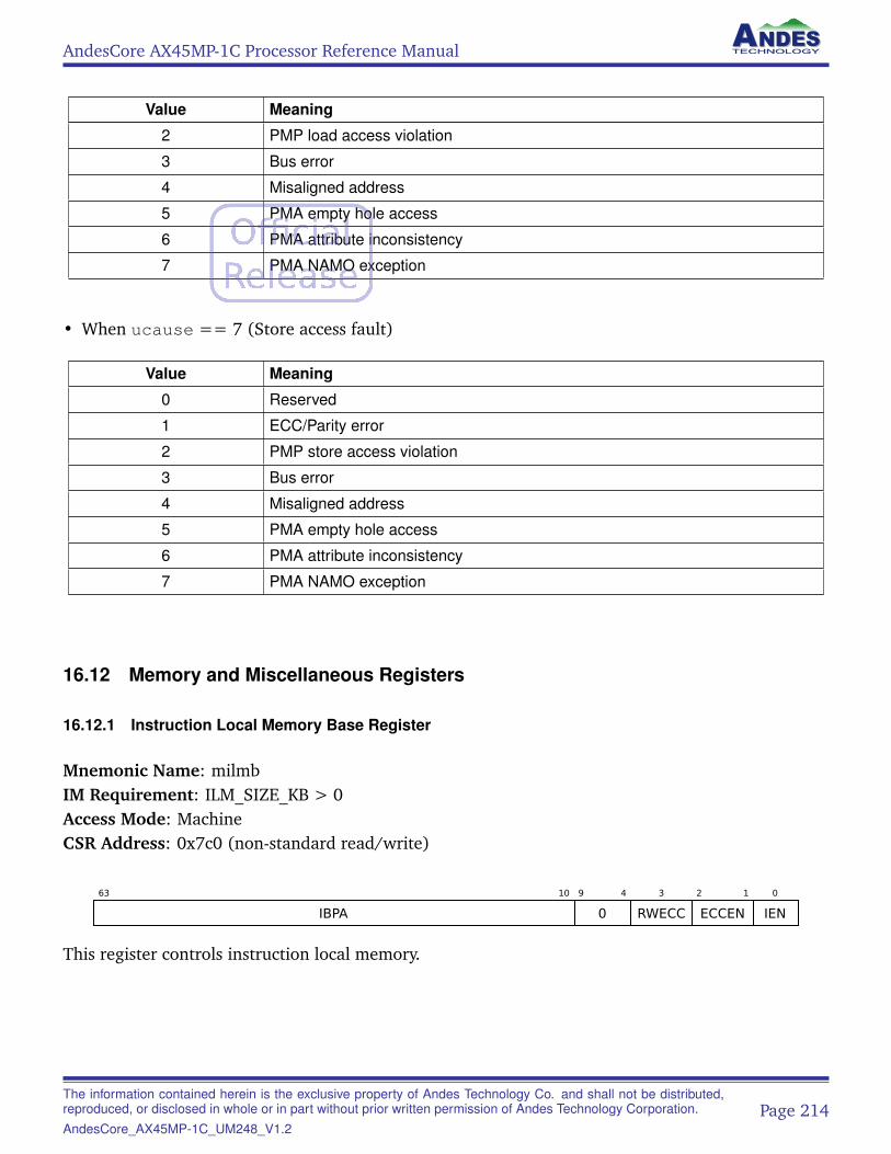
AndesCore AX45MP-1C Processor Reference Manual
Value Meaning
2 PMP load access violation
3 Bus error
4 Misaligned address
5 PMA empty hole access
6 PMA attribute inconsistency
7 PMA NAMO exception
• When ucause == 7 (Store access fault)
Value Meaning
0 Reserved
1 ECC/Parity error
2 PMP store access violation
3 Bus error
4 Misaligned address
5 PMA empty hole access
6 PMA attribute inconsistency
7 PMA NAMO exception
16.12 Memory and Miscellaneous Registers
16.12.1 Instruction Local Memory Base Register
Mnemonic Name: milmbIM Requirement: ILM_SIZE_KB > 0Access Mode: MachineCSR Address: 0x7c0 (non-standard read/write)
63 10
IBPA
9 4
0
3
RWECC
2 1
ECCEN
0
IEN
This register controls instruction local memory.
The information contained herein is the exclusive property of Andes Technology Co. and shall not be distributed,reproduced, or disclosed in whole or in part without prior written permission of Andes Technology Corporation.AndesCore_AX45MP-1C_UM248_V1.2
Page 214
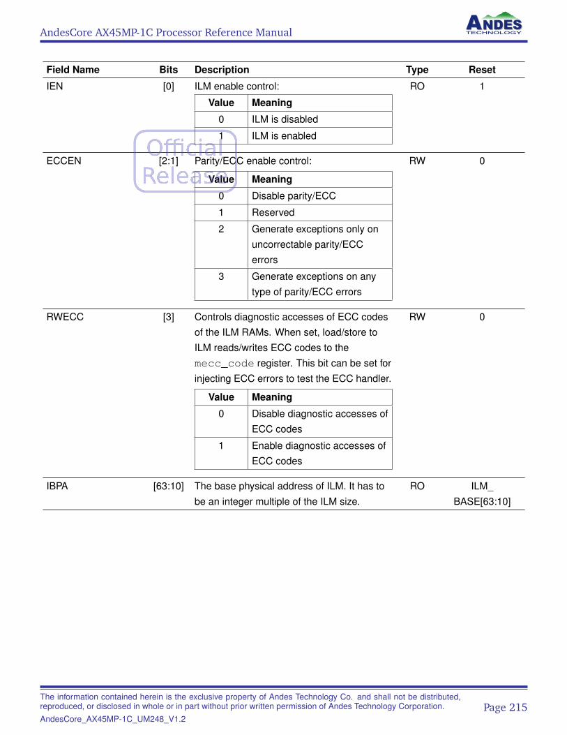
AndesCore AX45MP-1C Processor Reference Manual
Field Name Bits Description Type Reset
IEN [0] ILM enable control:
Value Meaning
0 ILM is disabled
1 ILM is enabled
RO 1
ECCEN [2:1] Parity/ECC enable control:
Value Meaning
0 Disable parity/ECC
1 Reserved
2 Generate exceptions only onuncorrectable parity/ECCerrors
3 Generate exceptions on anytype of parity/ECC errors
RW 0
RWECC [3] Controls diagnostic accesses of ECC codesof the ILM RAMs. When set, load/store toILM reads/writes ECC codes to themecc_code register. This bit can be set forinjecting ECC errors to test the ECC handler.
Value Meaning
0 Disable diagnostic accesses ofECC codes
1 Enable diagnostic accesses ofECC codes
RW 0
IBPA [63:10] The base physical address of ILM. It has tobe an integer multiple of the ILM size.
RO ILM_BASE[63:10]
The information contained herein is the exclusive property of Andes Technology Co. and shall not be distributed,reproduced, or disclosed in whole or in part without prior written permission of Andes Technology Corporation.AndesCore_AX45MP-1C_UM248_V1.2
Page 215
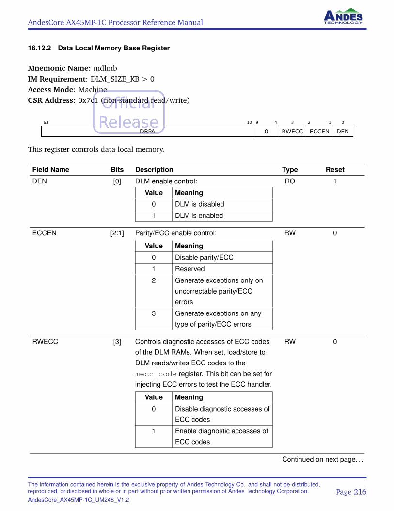
AndesCore AX45MP-1C Processor Reference Manual
16.12.2 Data Local Memory Base Register
Mnemonic Name: mdlmbIM Requirement: DLM_SIZE_KB > 0Access Mode: MachineCSR Address: 0x7c1 (non-standard read/write)
63 10
DBPA
9 4
0
3
RWECC
2 1
ECCEN
0
DEN
This register controls data local memory.
Field Name Bits Description Type Reset
DEN [0] DLM enable control:
Value Meaning
0 DLM is disabled
1 DLM is enabled
RO 1
ECCEN [2:1] Parity/ECC enable control:
Value Meaning
0 Disable parity/ECC
1 Reserved
2 Generate exceptions only onuncorrectable parity/ECCerrors
3 Generate exceptions on anytype of parity/ECC errors
RW 0
RWECC [3] Controls diagnostic accesses of ECC codesof the DLM RAMs. When set, load/store toDLM reads/writes ECC codes to themecc_code register. This bit can be set forinjecting ECC errors to test the ECC handler.
Value Meaning
0 Disable diagnostic accesses ofECC codes
1 Enable diagnostic accesses ofECC codes
RW 0
Continued on next page. . .
The information contained herein is the exclusive property of Andes Technology Co. and shall not be distributed,reproduced, or disclosed in whole or in part without prior written permission of Andes Technology Corporation.AndesCore_AX45MP-1C_UM248_V1.2
Page 216
AndesCore AX45MP-1C Processor Reference Manual
Field Name Bits Description Type Reset
DBPA [63:10] The base physical address of DLM. It has tobe an integer multiple of the DLM size.
RO DLM_BASE[63:10]
The information contained herein is the exclusive property of Andes Technology Co. and shall not be distributed,reproduced, or disclosed in whole or in part without prior written permission of Andes Technology Corporation.AndesCore_AX45MP-1C_UM248_V1.2
Page 217
AndesCore AX45MP-1C Processor Reference Manual
16.12.3 ECC Code Register
Mnemonic Name: mecc_codeIM Requirement: mmsc_cfg.ECC == 1Access Mode: MachineCSR Address: 0x7c2 (non-standard read/write)
63 23
0
22
INSN
21 18
RAMID
17
P
16
C
15 8
0
7 0
CODE
This register is used for accessing ECC array.
Field Name Bits Description Type Reset
CODE [7:0] This field records the ECC value on ECC errorexceptions. This field is also used to read/writethe ECC codes when diagnostic access of ECCcodes are enabled (milmb.RWECC or mdlmb.RWECC is 1).
RW 0
C [16] Correctable error. This bit is updated onparity/ECC error exceptions.
Value Meaning
0 Uncorrectable error
1 Correctable error
RO 0
P [17] Precise error. This bit is updated on parity/ECCerror exceptions.
Value Meaning
0 Imprecise error
1 Precise error
RO 0
Continued on next page. . .
The information contained herein is the exclusive property of Andes Technology Co. and shall not be distributed,reproduced, or disclosed in whole or in part without prior written permission of Andes Technology Corporation.AndesCore_AX45MP-1C_UM248_V1.2
Page 218
AndesCore AX45MP-1C Processor Reference Manual
Field Name Bits Description Type Reset
RAMID [21:18] The ID of RAM that caused parity/ECC errors.This bit is updated on parity/ECC errorexceptions.
Value Meaning
0–1 Reserved
2 Tag RAM of I-Cache
3 Data RAM of I-Cache
4 Tag RAM of D-Cache
5 Data RAM of D-Cache
6 Tag RAM of TLB
7 Data RAM of TLB
8 ILM
9 DLM
10–15 Reserved
RO 0
INSN [22] Indicates if the parity/ECC error is caused byinstruction fetch or data access.
Value Meaning
0 Data access
1 Instruction fetch
RO 0
The information contained herein is the exclusive property of Andes Technology Co. and shall not be distributed,reproduced, or disclosed in whole or in part without prior written permission of Andes Technology Corporation.AndesCore_AX45MP-1C_UM248_V1.2
Page 219
AndesCore AX45MP-1C Processor Reference Manual
16.12.4 NMI Vector Base Address Register
Mnemonic Name: mnvecIM Requirement: RequiredAccess Mode: MachineCSR Address: 0x7c3 (non-standard read/write)
63 0
MNVEC
This register indicates the entry point when an NMI occurs.
Field Name Bits Description Type Reset
MNVEC [63:0] Base address of the NMI handler. Its valueis the program starting address when NMIoccurs.
RO Pin Configured
The information contained herein is the exclusive property of Andes Technology Co. and shall not be distributed,reproduced, or disclosed in whole or in part without prior written permission of Andes Technology Corporation.AndesCore_AX45MP-1C_UM248_V1.2
Page 220
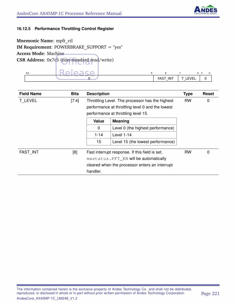
AndesCore AX45MP-1C Processor Reference Manual
16.12.5 Performance Throttling Control Register
Mnemonic Name: mpft_ctlIM Requirement: POWERBRAKE_SUPPORT = "yes"Access Mode: MachineCSR Address: 0x7c5 (non-standard read/write)
63 9
0
8
FAST_INT
7 4
T_LEVEL
3 0
0
Field Name Bits Description Type Reset
T_LEVEL [7:4] Throttling Level. The processor has the highestperformance at throttling level 0 and the lowestperformance at throttling level 15.
Value Meaning
0 Level 0 (the highest performance)
1-14 Level 1-14
15 Level 15 (the lowest performance)
RW 0
FAST_INT [8] Fast interrupt response. If this field is set,mxstatus.PFT_EN will be automaticallycleared when the processor enters an interrupthandler.
RW 0
The information contained herein is the exclusive property of Andes Technology Co. and shall not be distributed,reproduced, or disclosed in whole or in part without prior written permission of Andes Technology Corporation.AndesCore_AX45MP-1C_UM248_V1.2
Page 221
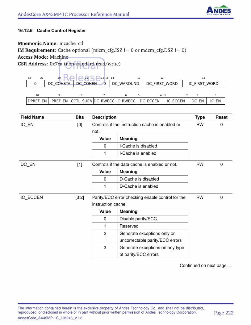
AndesCore AX45MP-1C Processor Reference Manual
16.12.6 Cache Control Register
Mnemonic Name: mcache_ctlIM Requirement: Cache optional (micm_cfg.ISZ != 0 or mdcm_cfg.DSZ != 0)Access Mode: MachineCSR Address: 0x7ca (non-standard read/write)
63 21
0
20
DC_COHSTA
19
DC_COHEN
18 15
0
14 13
DC_WAROUND
12
DC_FIRST_WORD
11
IC_FIRST_WORD
10
DPREF_EN
9
IPREF_EN
8
CCTL_SUEN
7
DC_RWECC
6
IC_RWECC
5 4
DC_ECCEN
3 2
IC_ECCEN
1
DC_EN
0
IC_EN
Field Name Bits Description Type Reset
IC_EN [0] Controls if the instruction cache is enabled ornot.
Value Meaning
0 I-Cache is disabled
1 I-Cache is enabled
RW 0
DC_EN [1] Controls if the data cache is enabled or not.
Value Meaning
0 D-Cache is disabled
1 D-Cache is enabled
RW 0
IC_ECCEN [3:2] Parity/ECC error checking enable control for theinstruction cache.
Value Meaning
0 Disable parity/ECC
1 Reserved
2 Generate exceptions only onuncorrectable parity/ECC errors
3 Generate exceptions on any typeof parity/ECC errors
RW 0
Continued on next page. . .
The information contained herein is the exclusive property of Andes Technology Co. and shall not be distributed,reproduced, or disclosed in whole or in part without prior written permission of Andes Technology Corporation.AndesCore_AX45MP-1C_UM248_V1.2
Page 222
AndesCore AX45MP-1C Processor Reference Manual
Field Name Bits Description Type Reset
DC_ECCEN [5:4] Parity/ECC error checking enable control for thedata cache.
Value Meaning
0 Disable parity/ECC
1 Reserved
2 Generate exceptions only onuncorrectable parity/ECC errors
3 Generate exceptions on any typeof parity/ECC errors
RW 0
IC_RWECC [6] Controls diagnostic accesses of ECC codes ofthe instruction cache RAMs. It is set to enableCCTL operations to access the ECC codes (seeSection 7.6). This bit can be set for injectingECC errors to test the ECC handler.
Value Meaning
0 Disable diagnostic accesses ofECC codes
1 Enable diagnostic accesses ofECC codes
RW 0
DC_RWECC [7] Controls diagnostic accesses of ECC codes ofthe data cache RAMs. It is set to enable CCTLoperations to access the ECC codes (seeSection 7.6). This bit can be set for injectingECC errors to test the ECC handler.
Value Meaning
0 Disable diagnostic accesses ofECC codes
1 Enable diagnostic accesses ofECC codes
RW 0
Continued on next page. . .
The information contained herein is the exclusive property of Andes Technology Co. and shall not be distributed,reproduced, or disclosed in whole or in part without prior written permission of Andes Technology Corporation.AndesCore_AX45MP-1C_UM248_V1.2
Page 223
AndesCore AX45MP-1C Processor Reference Manual
Field Name Bits Description Type Reset
CCTL_SUEN [8] Enable bit for Superuser-mode and User-modesoftware to access ucctlbeginaddr anducctlcommand CSRs.
Value Meaning
0 Disable ucctlbeginaddr anducctlcommand accesses inS/U mode
1 Enable ucctlbeginaddr anducctlcommand accesses inS/U mode
RW 0
IPREF_EN [9] This bit controls hardware prefetch for instructionfetches to cacheable memory regions whenI-Cache size is not 0.
Value Meaning
0 Disable hardware prefetch oninstruction fetches
1 Enable hardware prefetch oninstruction fetches
RW 0
DPREF_EN [10] This bit controls hardware prefetch for load/storeaccesses to cacheable memory regions whenD-Cache size is not 0.
Value Meaning
0 Disable hardware prefetch onload/store memory accesses.
1 Enable hardware prefetch onload/store memory accesses.
RW 0
IC_FIRST_WORD [11] I-Cache miss allocation filling policy
Value Meaning
0 Cache line data is returned critical(double) word first
1 Cache line data is returned thelowest address (double) word first
RO 1
Continued on next page. . .
The information contained herein is the exclusive property of Andes Technology Co. and shall not be distributed,reproduced, or disclosed in whole or in part without prior written permission of Andes Technology Corporation.AndesCore_AX45MP-1C_UM248_V1.2
Page 224
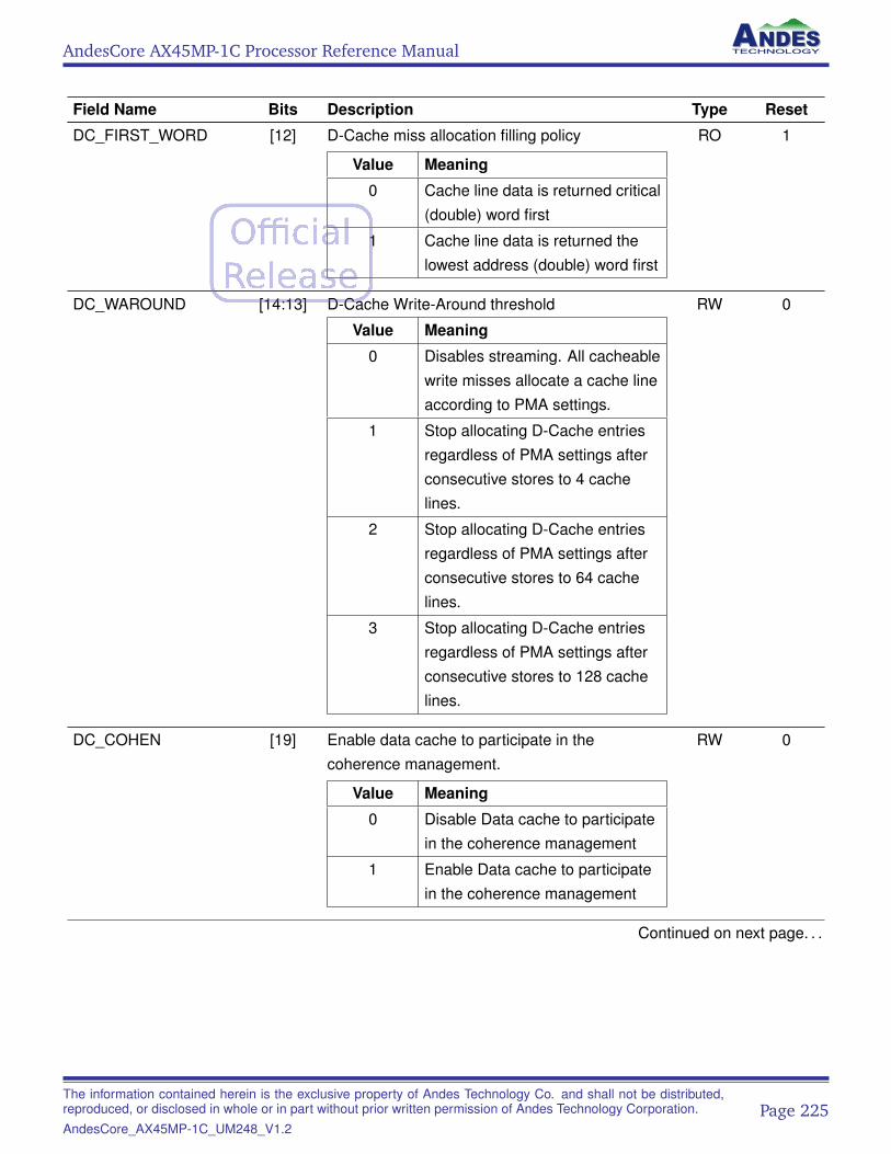
AndesCore AX45MP-1C Processor Reference Manual
Field Name Bits Description Type Reset
DC_FIRST_WORD [12] D-Cache miss allocation filling policy
Value Meaning
0 Cache line data is returned critical(double) word first
1 Cache line data is returned thelowest address (double) word first
RO 1
DC_WAROUND [14:13] D-Cache Write-Around threshold
Value Meaning
0 Disables streaming. All cacheablewrite misses allocate a cache lineaccording to PMA settings.
1 Stop allocating D-Cache entriesregardless of PMA settings afterconsecutive stores to 4 cachelines.
2 Stop allocating D-Cache entriesregardless of PMA settings afterconsecutive stores to 64 cachelines.
3 Stop allocating D-Cache entriesregardless of PMA settings afterconsecutive stores to 128 cachelines.
RW 0
DC_COHEN [19] Enable data cache to participate in thecoherence management.
Value Meaning
0 Disable Data cache to participatein the coherence management
1 Enable Data cache to participatein the coherence management
RW 0
Continued on next page. . .
The information contained herein is the exclusive property of Andes Technology Co. and shall not be distributed,reproduced, or disclosed in whole or in part without prior written permission of Andes Technology Corporation.AndesCore_AX45MP-1C_UM248_V1.2
Page 225
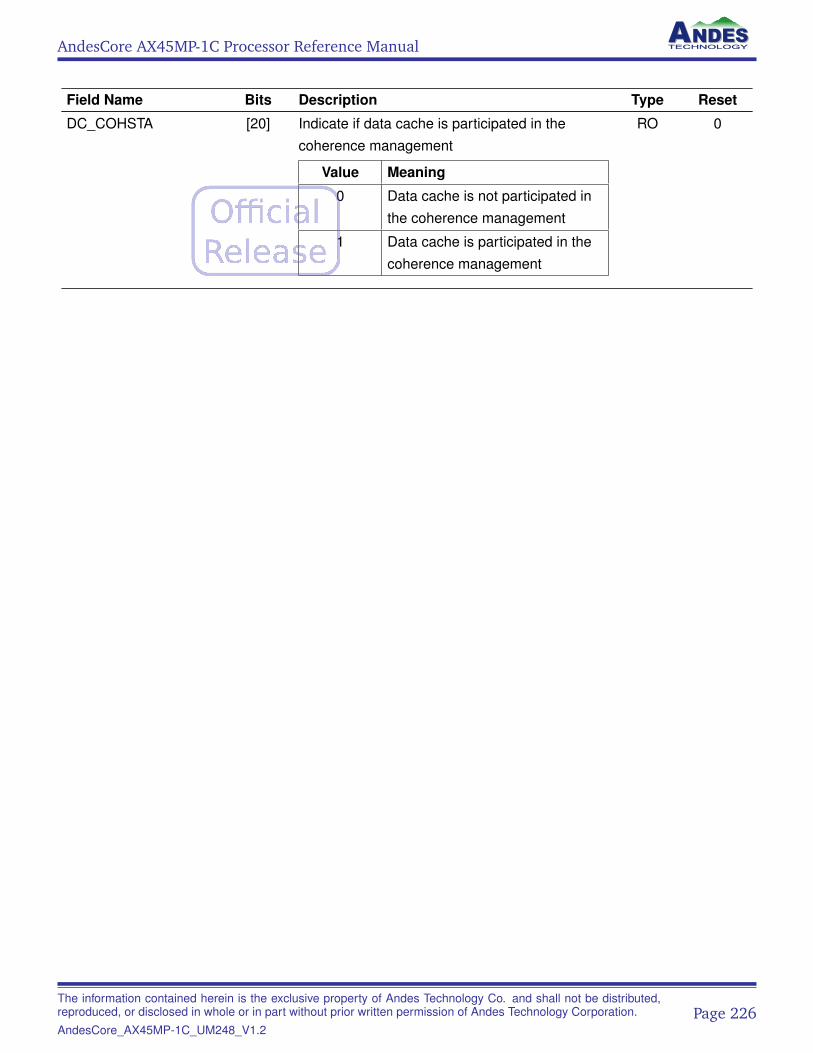
AndesCore AX45MP-1C Processor Reference Manual
Field Name Bits Description Type Reset
DC_COHSTA [20] Indicate if data cache is participated in thecoherence management
Value Meaning
0 Data cache is not participated inthe coherence management
1 Data cache is participated in thecoherence management
RO 0
The information contained herein is the exclusive property of Andes Technology Co. and shall not be distributed,reproduced, or disclosed in whole or in part without prior written permission of Andes Technology Corporation.AndesCore_AX45MP-1C_UM248_V1.2
Page 226
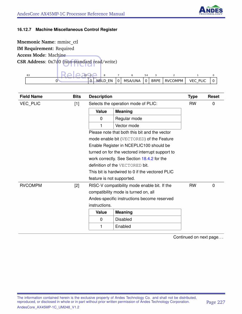
AndesCore AX45MP-1C Processor Reference Manual
16.12.7 Machine Miscellaneous Control Register
Mnemonic Name: mmisc_ctlIM Requirement: RequiredAccess Mode: MachineCSR Address: 0x7d0 (non-standard read/write)
63 10
0
9
0
8
NBLD_EN
7
0
6
MSA/UNA
54
0
3
BRPE
2
RVCOMPM
1
VEC_PLIC
0
0
Field Name Bits Description Type Reset
VEC_PLIC [1] Selects the operation mode of PLIC:
Value Meaning
0 Regular mode
1 Vector mode
Please note that both this bit and the vectormode enable bit (VECTORED) of the FeatureEnable Register in NCEPLIC100 should beturned on for the vectored interrupt support towork correctly. See Section 18.4.2 for thedefinition of the VECTORED bit.This bit is hardwired to 0 if the vectored PLICfeature is not supported.
RW 0
RVCOMPM [2] RISC-V compatibility mode enable bit. If thecompatibility mode is turned on, allAndes-specific instructions become reservedinstructions.
Value Meaning
0 Disabled
1 Enabled
RW 0
Continued on next page. . .
The information contained herein is the exclusive property of Andes Technology Co. and shall not be distributed,reproduced, or disclosed in whole or in part without prior written permission of Andes Technology Corporation.AndesCore_AX45MP-1C_UM248_V1.2
Page 227
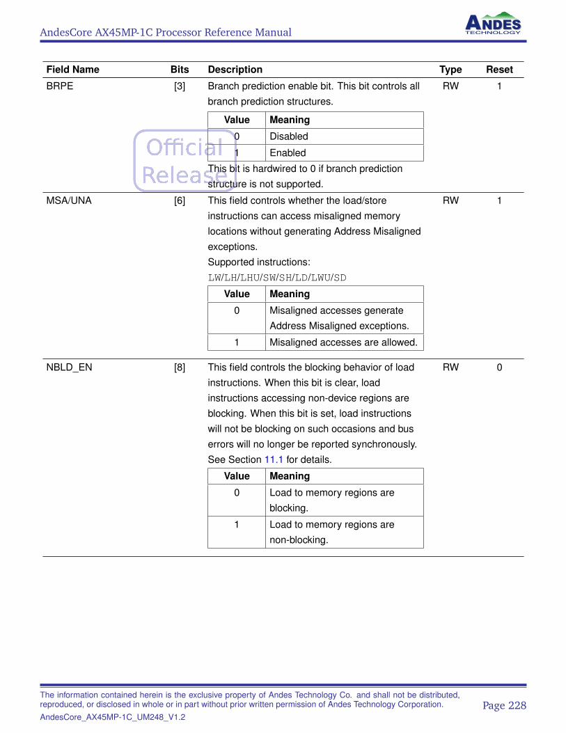
AndesCore AX45MP-1C Processor Reference Manual
Field Name Bits Description Type Reset
BRPE [3] Branch prediction enable bit. This bit controls allbranch prediction structures.
Value Meaning
0 Disabled
1 Enabled
This bit is hardwired to 0 if branch predictionstructure is not supported.
RW 1
MSA/UNA [6] This field controls whether the load/storeinstructions can access misaligned memorylocations without generating Address Misalignedexceptions.Supported instructions:LW/LH/LHU/SW/SH/LD/LWU/SD
Value Meaning
0 Misaligned accesses generateAddress Misaligned exceptions.
1 Misaligned accesses are allowed.
RW 1
NBLD_EN [8] This field controls the blocking behavior of loadinstructions. When this bit is clear, loadinstructions accessing non-device regions areblocking. When this bit is set, load instructionswill not be blocking on such occasions and buserrors will no longer be reported synchronously.See Section 11.1 for details.
Value Meaning
0 Load to memory regions areblocking.
1 Load to memory regions arenon-blocking.
RW 0
The information contained herein is the exclusive property of Andes Technology Co. and shall not be distributed,reproduced, or disclosed in whole or in part without prior written permission of Andes Technology Corporation.AndesCore_AX45MP-1C_UM248_V1.2
Page 228
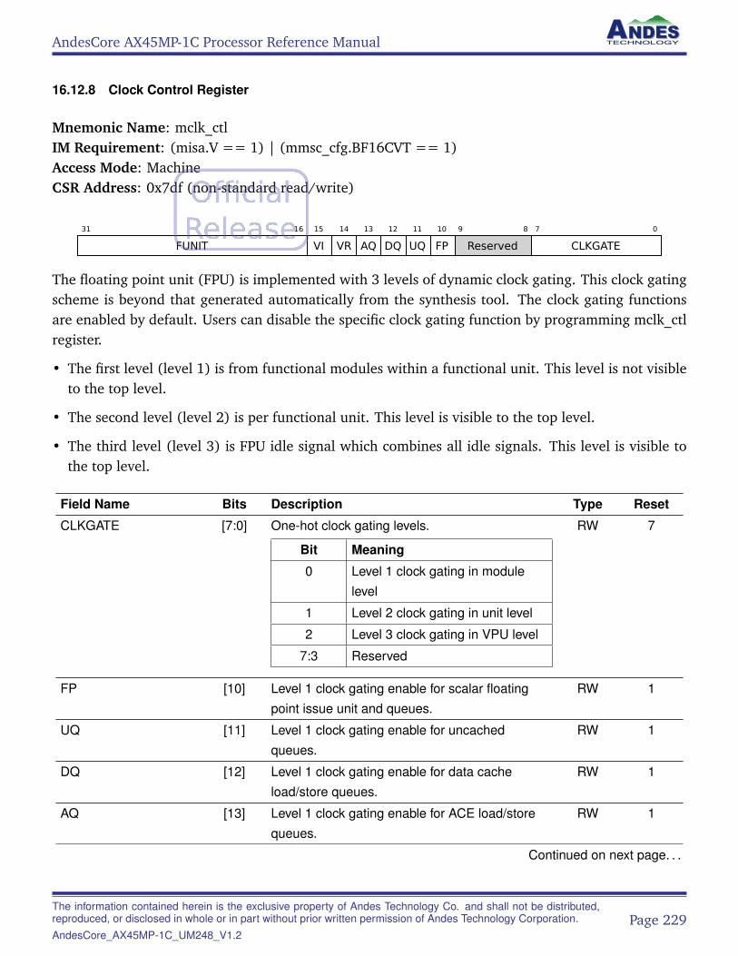
AndesCore AX45MP-1C Processor Reference Manual
16.12.8 Clock Control Register
Mnemonic Name: mclk_ctlIM Requirement: (misa.V == 1) | (mmsc_cfg.BF16CVT == 1)Access Mode: MachineCSR Address: 0x7df (non-standard read/write)
31 16
FUNIT
15
VI
14
VR
13
AQ
12
DQ
11
UQ
10
FP
9 8
Reserved
7 0
CLKGATE
The floating point unit (FPU) is implemented with 3 levels of dynamic clock gating. This clock gatingscheme is beyond that generated automatically from the synthesis tool. The clock gating functionsare enabled by default. Users can disable the specific clock gating function by programming mclk_ctlregister.
• The first level (level 1) is from functional modules within a functional unit. This level is not visibleto the top level.
• The second level (level 2) is per functional unit. This level is visible to the top level.
• The third level (level 3) is FPU idle signal which combines all idle signals. This level is visible tothe top level.
Field Name Bits Description Type Reset
CLKGATE [7:0] One-hot clock gating levels.
Bit Meaning
0 Level 1 clock gating in modulelevel
1 Level 2 clock gating in unit level
2 Level 3 clock gating in VPU level
7:3 Reserved
RW 7
FP [10] Level 1 clock gating enable for scalar floatingpoint issue unit and queues.
RW 1
UQ [11] Level 1 clock gating enable for uncachedqueues.
RW 1
DQ [12] Level 1 clock gating enable for data cacheload/store queues.
RW 1
AQ [13] Level 1 clock gating enable for ACE load/storequeues.
RW 1
Continued on next page. . .
The information contained herein is the exclusive property of Andes Technology Co. and shall not be distributed,reproduced, or disclosed in whole or in part without prior written permission of Andes Technology Corporation.AndesCore_AX45MP-1C_UM248_V1.2
Page 229
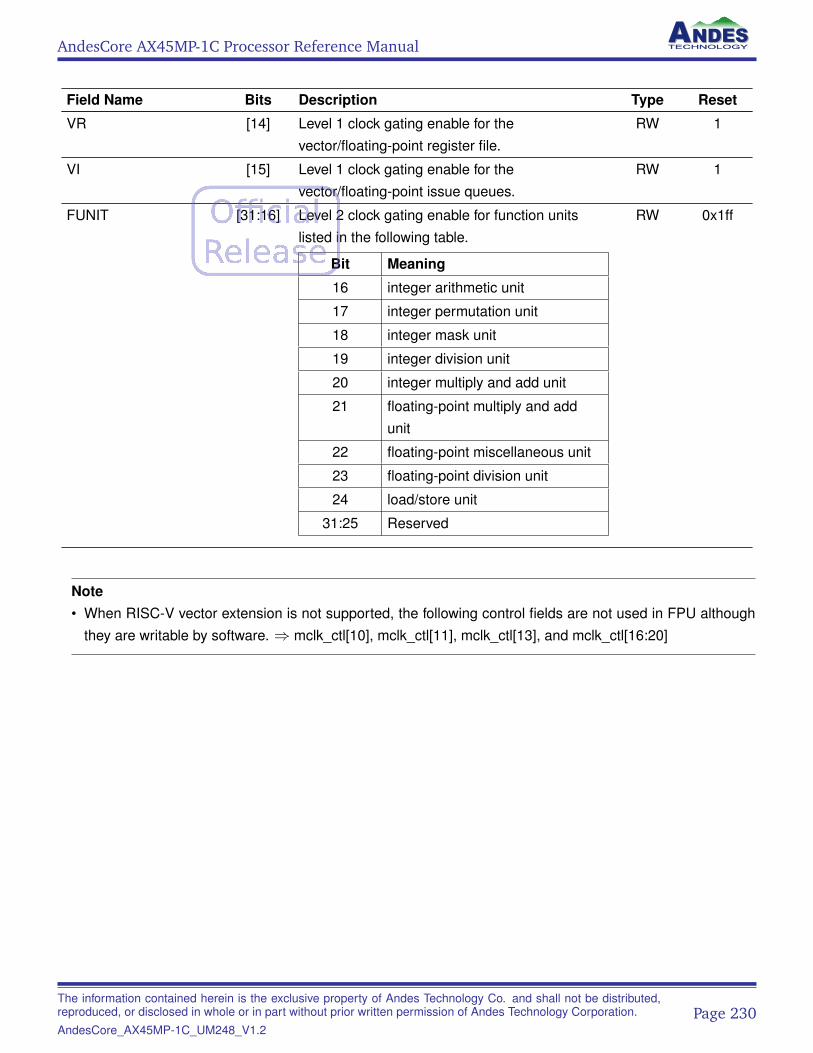
AndesCore AX45MP-1C Processor Reference Manual
Field Name Bits Description Type Reset
VR [14] Level 1 clock gating enable for thevector/floating-point register file.
RW 1
VI [15] Level 1 clock gating enable for thevector/floating-point issue queues.
RW 1
FUNIT [31:16] Level 2 clock gating enable for function unitslisted in the following table.
Bit Meaning
16 integer arithmetic unit
17 integer permutation unit
18 integer mask unit
19 integer division unit
20 integer multiply and add unit
21 floating-point multiply and addunit
22 floating-point miscellaneous unit
23 floating-point division unit
24 load/store unit
31:25 Reserved
RW 0x1ff
Note• When RISC-V vector extension is not supported, the following control fields are not used in FPU although
they are writable by software. ⇒ mclk_ctl[10], mclk_ctl[11], mclk_ctl[13], and mclk_ctl[16:20]
The information contained herein is the exclusive property of Andes Technology Co. and shall not be distributed,reproduced, or disclosed in whole or in part without prior written permission of Andes Technology Corporation.AndesCore_AX45MP-1C_UM248_V1.2
Page 230
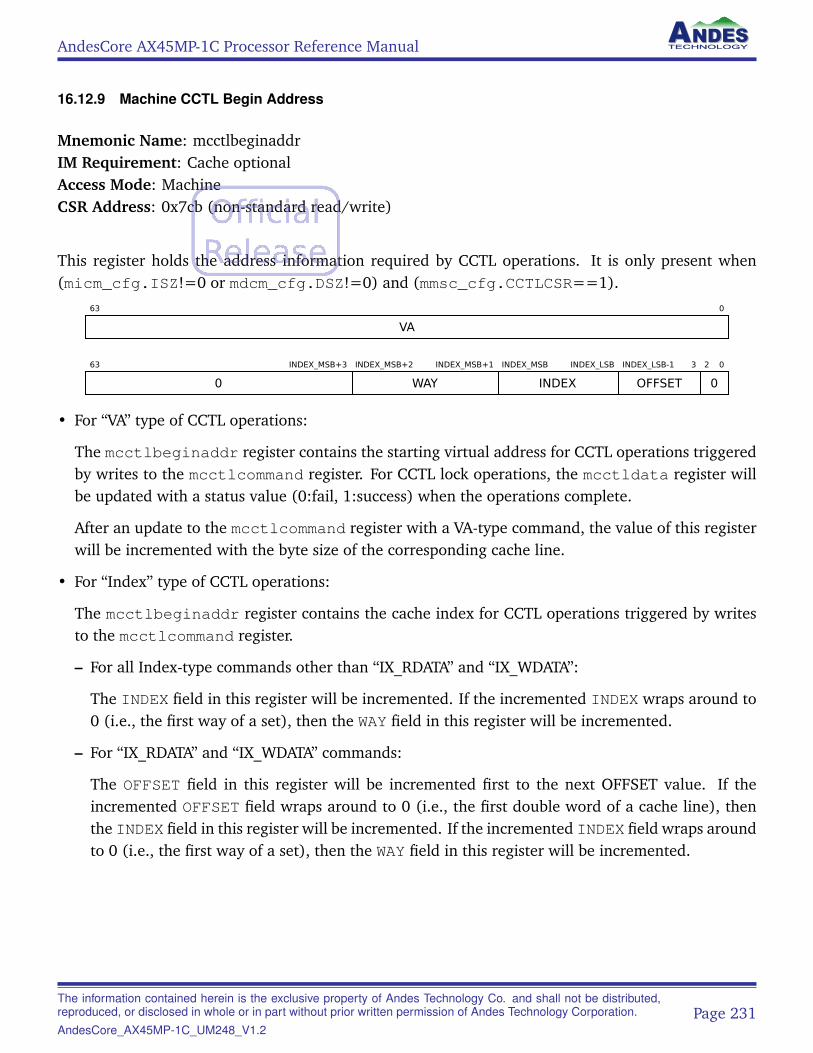
AndesCore AX45MP-1C Processor Reference Manual
16.12.9 Machine CCTL Begin Address
Mnemonic Name: mcctlbeginaddrIM Requirement: Cache optionalAccess Mode: MachineCSR Address: 0x7cb (non-standard read/write)
This register holds the address information required by CCTL operations. It is only present when(micm_cfg.ISZ!=0 or mdcm_cfg.DSZ!=0) and (mmsc_cfg.CCTLCSR==1).
63 0
VA
63 INDEX_MSB+3
0
INDEX_MSB+2 INDEX_MSB+1
WAY
INDEX_MSB INDEX_LSB
INDEX
INDEX_LSB-1 3
OFFSET
2 0
0
• For “VA” type of CCTL operations:
The mcctlbeginaddr register contains the starting virtual address for CCTL operations triggeredby writes to the mcctlcommand register. For CCTL lock operations, the mcctldata register willbe updated with a status value (0:fail, 1:success) when the operations complete.
After an update to the mcctlcommand register with a VA-type command, the value of this registerwill be incremented with the byte size of the corresponding cache line.
• For “Index” type of CCTL operations:
The mcctlbeginaddr register contains the cache index for CCTL operations triggered by writesto the mcctlcommand register.
– For all Index-type commands other than “IX_RDATA” and “IX_WDATA”:
The INDEX field in this register will be incremented. If the incremented INDEX wraps around to0 (i.e., the first way of a set), then the WAY field in this register will be incremented.
– For “IX_RDATA” and “IX_WDATA” commands:
The OFFSET field in this register will be incremented first to the next OFFSET value. If theincremented OFFSET field wraps around to 0 (i.e., the first double word of a cache line), thenthe INDEX field in this register will be incremented. If the incremented INDEX field wraps aroundto 0 (i.e., the first way of a set), then the WAY field in this register will be incremented.
The information contained herein is the exclusive property of Andes Technology Co. and shall not be distributed,reproduced, or disclosed in whole or in part without prior written permission of Andes Technology Corporation.AndesCore_AX45MP-1C_UM248_V1.2
Page 231
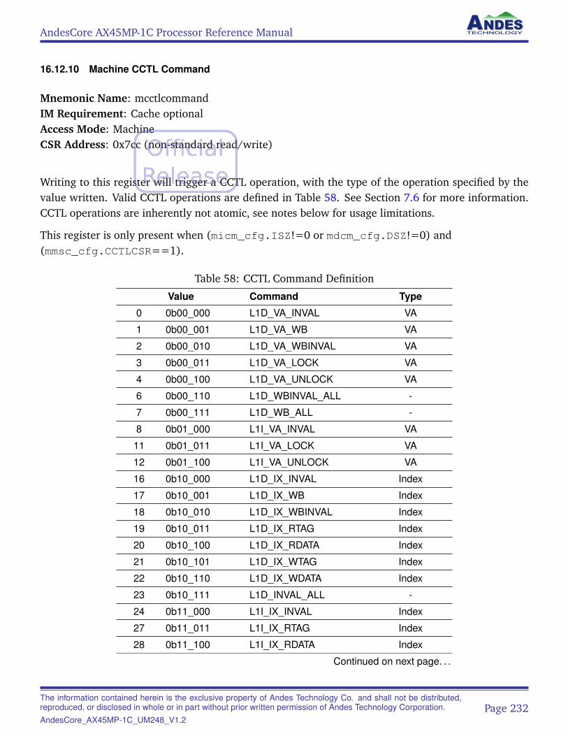
AndesCore AX45MP-1C Processor Reference Manual
16.12.10 Machine CCTL Command
Mnemonic Name: mcctlcommandIM Requirement: Cache optionalAccess Mode: MachineCSR Address: 0x7cc (non-standard read/write)
Writing to this register will trigger a CCTL operation, with the type of the operation specified by thevalue written. Valid CCTL operations are defined in Table 58. See Section 7.6 for more information.CCTL operations are inherently not atomic, see notes below for usage limitations.
This register is only present when (micm_cfg.ISZ!=0 or mdcm_cfg.DSZ!=0) and(mmsc_cfg.CCTLCSR==1).
Table 58: CCTL Command Definition
Value Command Type
0 0b00_000 L1D_VA_INVAL VA
1 0b00_001 L1D_VA_WB VA
2 0b00_010 L1D_VA_WBINVAL VA
3 0b00_011 L1D_VA_LOCK VA
4 0b00_100 L1D_VA_UNLOCK VA
6 0b00_110 L1D_WBINVAL_ALL -
7 0b00_111 L1D_WB_ALL -
8 0b01_000 L1I_VA_INVAL VA
11 0b01_011 L1I_VA_LOCK VA
12 0b01_100 L1I_VA_UNLOCK VA
16 0b10_000 L1D_IX_INVAL Index
17 0b10_001 L1D_IX_WB Index
18 0b10_010 L1D_IX_WBINVAL Index
19 0b10_011 L1D_IX_RTAG Index
20 0b10_100 L1D_IX_RDATA Index
21 0b10_101 L1D_IX_WTAG Index
22 0b10_110 L1D_IX_WDATA Index
23 0b10_111 L1D_INVAL_ALL -
24 0b11_000 L1I_IX_INVAL Index
27 0b11_011 L1I_IX_RTAG Index
28 0b11_100 L1I_IX_RDATA Index
Continued on next page. . .
The information contained herein is the exclusive property of Andes Technology Co. and shall not be distributed,reproduced, or disclosed in whole or in part without prior written permission of Andes Technology Corporation.AndesCore_AX45MP-1C_UM248_V1.2
Page 232
AndesCore AX45MP-1C Processor Reference Manual
Table 58: (continued)
Value Command Type
29 0b11_101 L1I_IX_WTAG Index
30 0b11_110 L1I_IX_WDATA Index
NoteCCTL operations take parameters from multiple CSR registers, thus they are inherently not atomic. In ad-dition, the CSRs share common storage across privilege levels, making them vulnerable to be overwrittenacross context switches. This implies that higher privilege level software should back up the content of CCTLCSR registers with interrupts disabled before using them, and restore their values afterwards if CCTL oper-ations will be invoked in multiple privilege levels. The same is true if CCTL operations will be used both innon-interrupt codes and in the interrupt handlers.
The information contained herein is the exclusive property of Andes Technology Co. and shall not be distributed,reproduced, or disclosed in whole or in part without prior written permission of Andes Technology Corporation.AndesCore_AX45MP-1C_UM248_V1.2
Page 233
AndesCore AX45MP-1C Processor Reference Manual
16.12.11 Machine CCTL Data
Mnemonic Name: mcctldataIM Requirement: Cache optionalAccess Mode: MachineCSR Address: 0x7cd (non-standard read/write)
This register holds data required/returned by some CCTL operations. It is only present when (micm_cfg.ISZ!=0 or mdcm_cfg.DSZ!=0) and (mmsc_cfg.CCTLCSR==1). The complete list of CCTLoperations are summarized in Table 59 and described below.
Table 59: CCTL Commands Which Access mcctldata
Value of mcctlcommand Command Type
3 0b00_011 L1D_VA_LOCK VA
11 0b01_011 L1I_VA_LOCK VA
19 0b10_011 L1D_IX_RTAG Index
20 0b10_100 L1D_IX_RDATA Index
21 0b10_101 L1D_IX_WTAG Index
22 0b10_110 L1D_IX_WDATA Index
27 0b11_011 L1I_IX_RTAG Index
28 0b11_100 L1I_IX_RDATA Index
29 0b11_101 L1I_IX_WTAG Index
30 0b11_110 L1I_IX_WDATA Index
• For CCTL lock operations: The mcctldata register will be updated with a status value (0: fail,1:success) when the operations complete.
• For CCTL index read/write-data operations: mcctldata[63:0] holds the cache data for the op-erations.
• For CCTL index read/write-tag operations, mcctldata register holds the cache tag for the opera-tions.
– The bit positions of the fields for I-Cache CCTL index read/write-tag is as follow:
* The TAG field does not hold every bits of PA[(PALEN-1):10] for the cache line. The cache tagRAMs do not hold all physical addresses down to bit 10. They only hold enough bits for taglook-ups. The unused lower order TAG bits will be reported as Don’t Care value for tag-readoperations and ignored on tag-write operations. The full PA value should be constructed usingthe corresponding index bits.
The information contained herein is the exclusive property of Andes Technology Co. and shall not be distributed,reproduced, or disclosed in whole or in part without prior written permission of Andes Technology Corporation.AndesCore_AX45MP-1C_UM248_V1.2
Page 234
AndesCore AX45MP-1C Processor Reference Manual
* I-Cache TAG RAM holds PA[(PA_LEN-1):A].
· A = min(12:(log2(micm_cfg.ISET)+6))
* If A is 11, bit 0 is unused. If A is 12, bit 0, 1 are unused.
* Bit XLEN-3 holds the duplicated lock bit for I-Cache to better tolerate soft-errors.
* Bit XLEN-2 holds the lock bit
* Bit XLEN-1 holds the valid bit.
– The bit positions of the fields for D-Cache CCTL index read/write-tag is as follow:
* MESI field holds the cache line status.
* Bit 3 holds the lock bit.
* The TAG field holds the tag data for the cache line. DTW =PALEN-6- log2(mdcm_cfg.DSET)
Table 60: I-Cache CCTL Index Read/Write TAG Bit Fields
Field Bit Position
TAG [0+:PALEN-11]
LOCK_DUP [XLEN-3]
LOCK [XLEN-2]
VALID [XLEN-1]
Table 61: D-Cache CCTL Index Read/Write TAG Bit Fields
Field Bit Position
MESI [0+:2]
LOCK [3]
TAG [4+:DTW]
The information contained herein is the exclusive property of Andes Technology Co. and shall not be distributed,reproduced, or disclosed in whole or in part without prior written permission of Andes Technology Corporation.AndesCore_AX45MP-1C_UM248_V1.2
Page 235
AndesCore AX45MP-1C Processor Reference Manual
16.12.12 Supervisor CCTL Data
Mnemonic Name: scctldataIM Requirement: Cache optionalAccess Mode: Supervisor and aboveCSR Address: 0x9cd (non-standard read/write)
This register is only present when ((micm_cfg.ISZ!=0 or mdcm_cfg.DSZ!=0) andmmsc_cfg.CCTLCSR==1 and misa[18]==1). It is an alias to the mcctldata register and it isonly accessible to Supervisor-mode software when mcache_ctl.CCTL_SUEN is 1. Otherwise illegalinstruction exceptions will be triggered.
Note• S-mode software triggers CCTL operations through writing the ucctlcommand register, and associated
addresses for the CCTL operations are specified in the ucctlbeginaddr register.• Due to the sharing of storage with mcctldata, interrupt-handler/M-mode software should back up mcctldata before use; see notes in Section 16.12.10 for usage limitations.
The information contained herein is the exclusive property of Andes Technology Co. and shall not be distributed,reproduced, or disclosed in whole or in part without prior written permission of Andes Technology Corporation.AndesCore_AX45MP-1C_UM248_V1.2
Page 236
AndesCore AX45MP-1C Processor Reference Manual
16.12.13 User CCTL Begin Address
Mnemonic Name: ucctlbeginaddrIM Requirement: Cache optionalAccess Mode: User and aboveCSR Address: 0x80b (non-standard read/write)
This register is only present when ((micm_cfg.ISZ!=0 or mdcm_cfg.DSZ!=0) andmmsc_cfg.CCTLCSR==1 and misa[20]==1). It is an alias to the mcctlbeginaddr register andit is only accessible to Supervisor-mode and User-mode software when mcache_ctl.CCTL_SUEN is1. Otherwise illegal instruction exceptions will be triggered.
Note• Both S-mode and U-mode software triggers CCTL operations through writing the ucctlcommand regis-
ter; the associated addresses for CCTL operations are specified in the ucctlbeginaddr register.• Due to the sharing of storage with mcctlbeginaddr, interrupt-handler/privileged-mode software should
back up mcctlbeginaddr before use; see notes in Section 16.12.10 for usage limitations.
The information contained herein is the exclusive property of Andes Technology Co. and shall not be distributed,reproduced, or disclosed in whole or in part without prior written permission of Andes Technology Corporation.AndesCore_AX45MP-1C_UM248_V1.2
Page 237
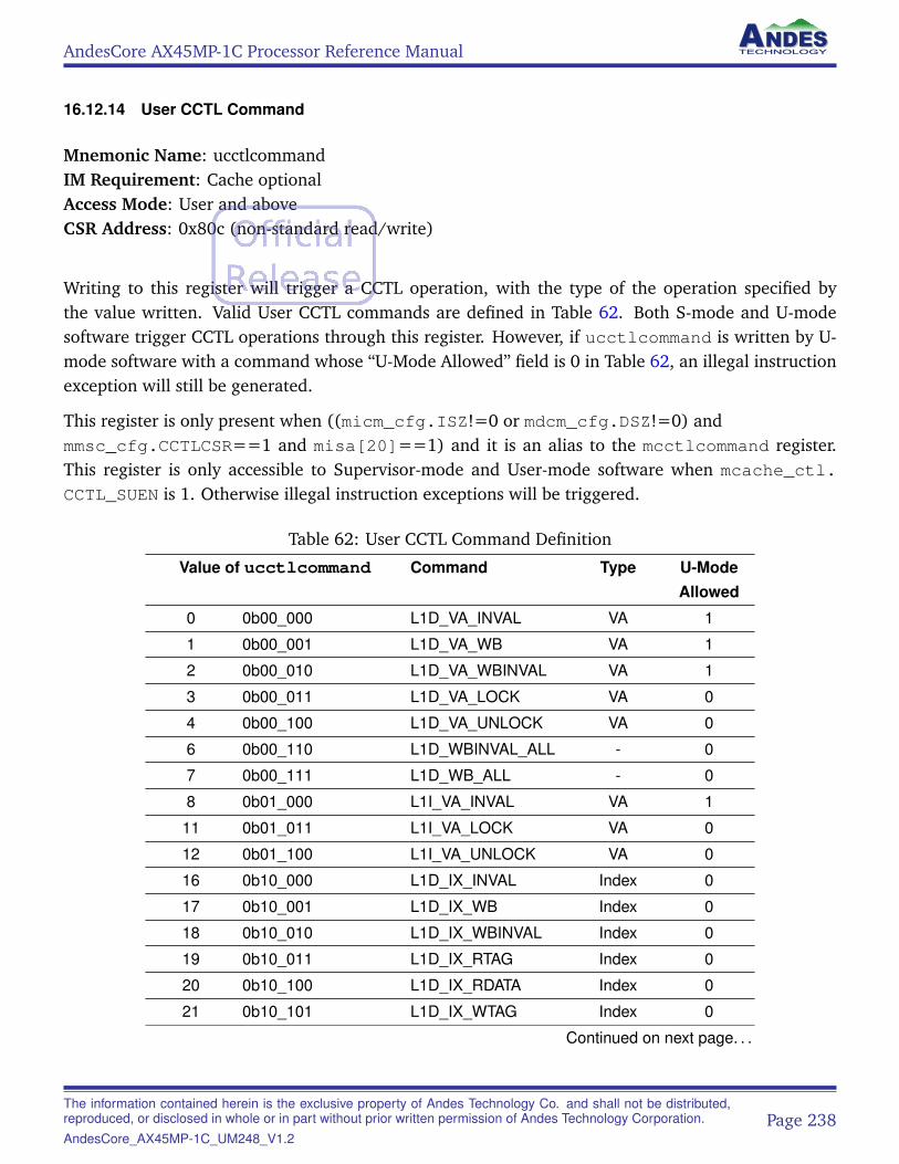
AndesCore AX45MP-1C Processor Reference Manual
16.12.14 User CCTL Command
Mnemonic Name: ucctlcommandIM Requirement: Cache optionalAccess Mode: User and aboveCSR Address: 0x80c (non-standard read/write)
Writing to this register will trigger a CCTL operation, with the type of the operation specified bythe value written. Valid User CCTL commands are defined in Table 62. Both S-mode and U-modesoftware trigger CCTL operations through this register. However, if ucctlcommand is written by U-mode software with a command whose “U-Mode Allowed” field is 0 in Table 62, an illegal instructionexception will still be generated.
This register is only present when ((micm_cfg.ISZ!=0 or mdcm_cfg.DSZ!=0) andmmsc_cfg.CCTLCSR==1 and misa[20]==1) and it is an alias to the mcctlcommand register.This register is only accessible to Supervisor-mode and User-mode software when mcache_ctl.
CCTL_SUEN is 1. Otherwise illegal instruction exceptions will be triggered.
Table 62: User CCTL Command Definition
Value of ucctlcommand Command Type U-ModeAllowed
0 0b00_000 L1D_VA_INVAL VA 1
1 0b00_001 L1D_VA_WB VA 1
2 0b00_010 L1D_VA_WBINVAL VA 1
3 0b00_011 L1D_VA_LOCK VA 0
4 0b00_100 L1D_VA_UNLOCK VA 0
6 0b00_110 L1D_WBINVAL_ALL - 0
7 0b00_111 L1D_WB_ALL - 0
8 0b01_000 L1I_VA_INVAL VA 1
11 0b01_011 L1I_VA_LOCK VA 0
12 0b01_100 L1I_VA_UNLOCK VA 0
16 0b10_000 L1D_IX_INVAL Index 0
17 0b10_001 L1D_IX_WB Index 0
18 0b10_010 L1D_IX_WBINVAL Index 0
19 0b10_011 L1D_IX_RTAG Index 0
20 0b10_100 L1D_IX_RDATA Index 0
21 0b10_101 L1D_IX_WTAG Index 0
Continued on next page. . .
The information contained herein is the exclusive property of Andes Technology Co. and shall not be distributed,reproduced, or disclosed in whole or in part without prior written permission of Andes Technology Corporation.AndesCore_AX45MP-1C_UM248_V1.2
Page 238
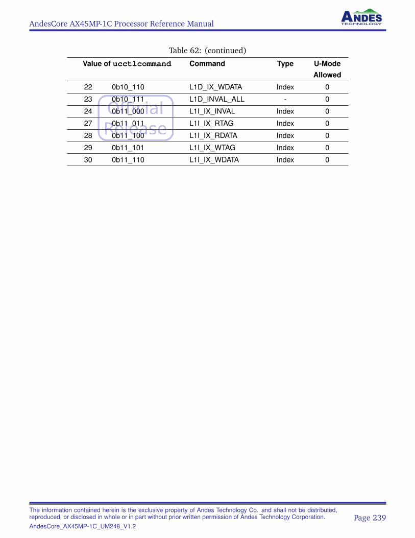
AndesCore AX45MP-1C Processor Reference Manual
Table 62: (continued)
Value of ucctlcommand Command Type U-ModeAllowed
22 0b10_110 L1D_IX_WDATA Index 0
23 0b10_111 L1D_INVAL_ALL - 0
24 0b11_000 L1I_IX_INVAL Index 0
27 0b11_011 L1I_IX_RTAG Index 0
28 0b11_100 L1I_IX_RDATA Index 0
29 0b11_101 L1I_IX_WTAG Index 0
30 0b11_110 L1I_IX_WDATA Index 0
The information contained herein is the exclusive property of Andes Technology Co. and shall not be distributed,reproduced, or disclosed in whole or in part without prior written permission of Andes Technology Corporation.AndesCore_AX45MP-1C_UM248_V1.2
Page 239
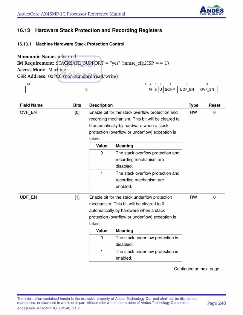
AndesCore AX45MP-1C Processor Reference Manual
16.13 Hardware Stack Protection and Recording Registers
16.13.1 Machine Hardware Stack Protection Control
Mnemonic Name: mhsp_ctlIM Requirement: STACKSAFE_SUPPORT = "yes" (mmsc_cfg.HSP == 1)Access Mode: MachineCSR Address: 0x7C6 (non-standard read/write)
63 6
0
5
M
4
S
3
U
2
SCHM
1
UDF_EN
0
OVF_EN
Field Name Bits Description Type Reset
OVF_EN [0] Enable bit for the stack overflow protection andrecording mechanism. This bit will be cleared to0 automatically by hardware when a stackprotection (overflow or underflow) exception istaken.
Value Meaning
0 The stack overflow protection andrecording mechanism aredisabled.
1 The stack overflow protection andrecording mechanism areenabled.
RW 0
UDF_EN [1] Enable bit for the stack underflow protectionmechanism. This bit will be cleared to 0automatically by hardware when a stackprotection (overflow or underflow) exception istaken.
Value Meaning
0 The stack underflow protection isdisabled.
1 The stack underflow protection isenabled.
RW 0
Continued on next page. . .
The information contained herein is the exclusive property of Andes Technology Co. and shall not be distributed,reproduced, or disclosed in whole or in part without prior written permission of Andes Technology Corporation.AndesCore_AX45MP-1C_UM248_V1.2
Page 240
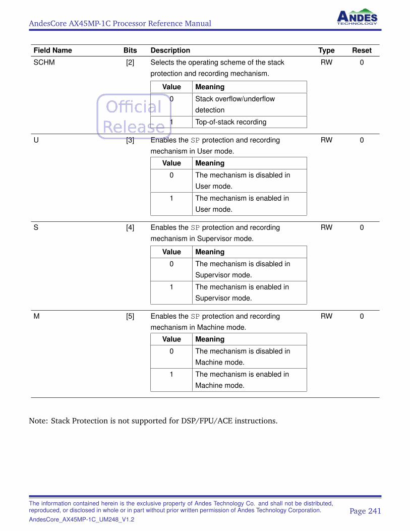
AndesCore AX45MP-1C Processor Reference Manual
Field Name Bits Description Type Reset
SCHM [2] Selects the operating scheme of the stackprotection and recording mechanism.
Value Meaning
0 Stack overflow/underflowdetection
1 Top-of-stack recording
RW 0
U [3] Enables the SP protection and recordingmechanism in User mode.
Value Meaning
0 The mechanism is disabled inUser mode.
1 The mechanism is enabled inUser mode.
RW 0
S [4] Enables the SP protection and recordingmechanism in Supervisor mode.
Value Meaning
0 The mechanism is disabled inSupervisor mode.
1 The mechanism is enabled inSupervisor mode.
RW 0
M [5] Enables the SP protection and recordingmechanism in Machine mode.
Value Meaning
0 The mechanism is disabled inMachine mode.
1 The mechanism is enabled inMachine mode.
RW 0
Note: Stack Protection is not supported for DSP/FPU/ACE instructions.
The information contained herein is the exclusive property of Andes Technology Co. and shall not be distributed,reproduced, or disclosed in whole or in part without prior written permission of Andes Technology Corporation.AndesCore_AX45MP-1C_UM248_V1.2
Page 241
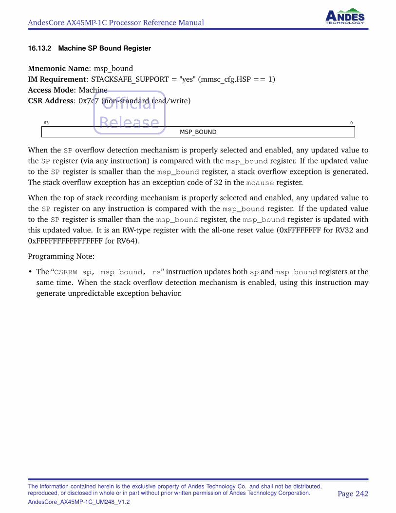
AndesCore AX45MP-1C Processor Reference Manual
16.13.2 Machine SP Bound Register
Mnemonic Name: msp_boundIM Requirement: STACKSAFE_SUPPORT = "yes" (mmsc_cfg.HSP == 1)Access Mode: MachineCSR Address: 0x7c7 (non-standard read/write)
63 0
MSP_BOUND
When the SP overflow detection mechanism is properly selected and enabled, any updated value tothe SP register (via any instruction) is compared with the msp_bound register. If the updated valueto the SP register is smaller than the msp_bound register, a stack overflow exception is generated.The stack overflow exception has an exception code of 32 in the mcause register.
When the top of stack recording mechanism is properly selected and enabled, any updated value tothe SP register on any instruction is compared with the msp_bound register. If the updated valueto the SP register is smaller than the msp_bound register, the msp_bound register is updated withthis updated value. It is an RW-type register with the all-one reset value (0xFFFFFFFF for RV32 and0xFFFFFFFFFFFFFFFF for RV64).
Programming Note:
• The “CSRRW sp, msp_bound, rs” instruction updates both sp and msp_bound registers at thesame time. When the stack overflow detection mechanism is enabled, using this instruction maygenerate unpredictable exception behavior.
The information contained herein is the exclusive property of Andes Technology Co. and shall not be distributed,reproduced, or disclosed in whole or in part without prior written permission of Andes Technology Corporation.AndesCore_AX45MP-1C_UM248_V1.2
Page 242
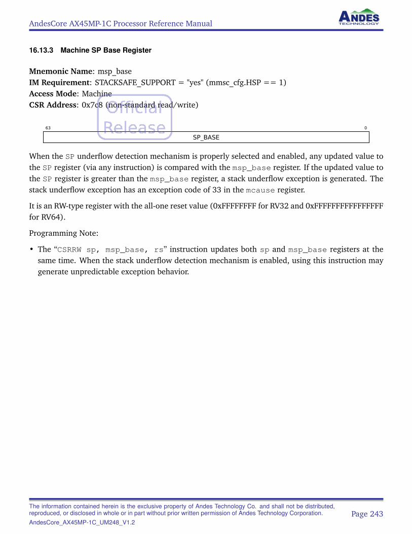
AndesCore AX45MP-1C Processor Reference Manual
16.13.3 Machine SP Base Register
Mnemonic Name: msp_baseIM Requirement: STACKSAFE_SUPPORT = "yes" (mmsc_cfg.HSP == 1)Access Mode: MachineCSR Address: 0x7c8 (non-standard read/write)
63 0
SP_BASE
When the SP underflow detection mechanism is properly selected and enabled, any updated value tothe SP register (via any instruction) is compared with the msp_base register. If the updated value tothe SP register is greater than the msp_base register, a stack underflow exception is generated. Thestack underflow exception has an exception code of 33 in the mcause register.
It is an RW-type register with the all-one reset value (0xFFFFFFFF for RV32 and 0xFFFFFFFFFFFFFFFFfor RV64).
Programming Note:
• The “CSRRW sp, msp_base, rs” instruction updates both sp and msp_base registers at thesame time. When the stack underflow detection mechanism is enabled, using this instruction maygenerate unpredictable exception behavior.
The information contained herein is the exclusive property of Andes Technology Co. and shall not be distributed,reproduced, or disclosed in whole or in part without prior written permission of Andes Technology Corporation.AndesCore_AX45MP-1C_UM248_V1.2
Page 243
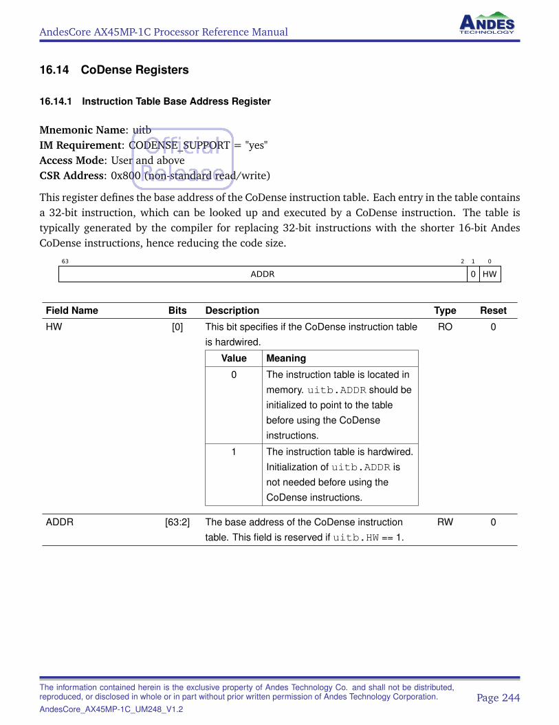
AndesCore AX45MP-1C Processor Reference Manual
16.14 CoDense Registers
16.14.1 Instruction Table Base Address Register
Mnemonic Name: uitbIM Requirement: CODENSE_SUPPORT = "yes"Access Mode: User and aboveCSR Address: 0x800 (non-standard read/write)
This register defines the base address of the CoDense instruction table. Each entry in the table containsa 32-bit instruction, which can be looked up and executed by a CoDense instruction. The table istypically generated by the compiler for replacing 32-bit instructions with the shorter 16-bit AndesCoDense instructions, hence reducing the code size.
63 2
ADDR
1
0
0
HW
Field Name Bits Description Type Reset
HW [0] This bit specifies if the CoDense instruction tableis hardwired.
Value Meaning
0 The instruction table is located inmemory. uitb.ADDR should beinitialized to point to the tablebefore using the CoDenseinstructions.
1 The instruction table is hardwired.Initialization of uitb.ADDR isnot needed before using theCoDense instructions.
RO 0
ADDR [63:2] The base address of the CoDense instructiontable. This field is reserved if uitb.HW == 1.
RW 0
The information contained herein is the exclusive property of Andes Technology Co. and shall not be distributed,reproduced, or disclosed in whole or in part without prior written permission of Andes Technology Corporation.AndesCore_AX45MP-1C_UM248_V1.2
Page 244
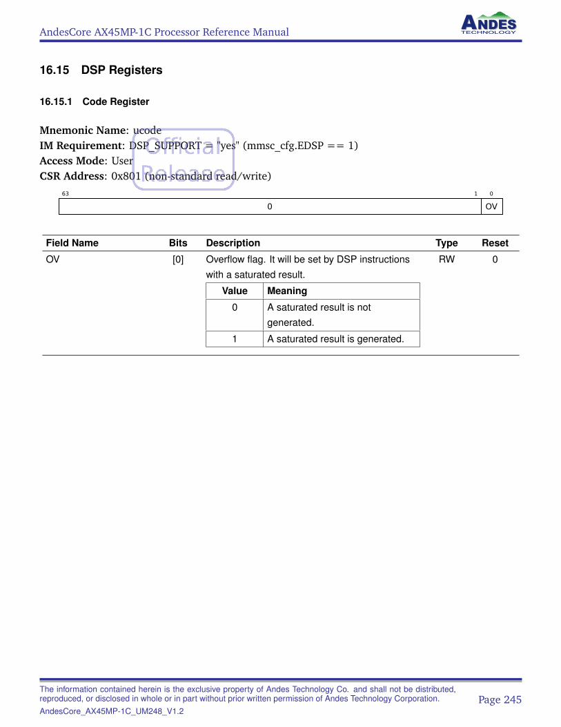
AndesCore AX45MP-1C Processor Reference Manual
16.15 DSP Registers
16.15.1 Code Register
Mnemonic Name: ucodeIM Requirement: DSP_SUPPORT = "yes" (mmsc_cfg.EDSP == 1)Access Mode: UserCSR Address: 0x801 (non-standard read/write)
63 1
0
0
OV
Field Name Bits Description Type Reset
OV [0] Overflow flag. It will be set by DSP instructionswith a saturated result.
Value Meaning
0 A saturated result is notgenerated.
1 A saturated result is generated.
RW 0
The information contained herein is the exclusive property of Andes Technology Co. and shall not be distributed,reproduced, or disclosed in whole or in part without prior written permission of Andes Technology Corporation.AndesCore_AX45MP-1C_UM248_V1.2
Page 245
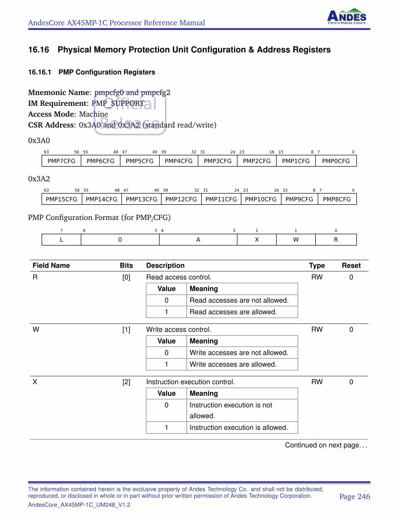
AndesCore AX45MP-1C Processor Reference Manual
16.16 Physical Memory Protection Unit Configuration & Address Registers
16.16.1 PMP Configuration Registers
Mnemonic Name: pmpcfg0 and pmpcfg2IM Requirement: PMP_SUPPORTAccess Mode: MachineCSR Address: 0x3A0 and 0x3A2 (standard read/write)
0x3A063 56
PMP7CFG
55 48
PMP6CFG
47 40
PMP5CFG
39 32
PMP4CFG
31 24
PMP3CFG
23 16
PMP2CFG
15 8
PMP1CFG
7 0
PMP0CFG
0x3A263 56
PMP15CFG
55 48
PMP14CFG
47 40
PMP13CFG
39 32
PMP12CFG
31 24
PMP11CFG
23 16
PMP10CFG
15 8
PMP9CFG
7 0
PMP8CFG
PMP Configuration Format (for PMPiCFG)
7
L
6 5
0
4 3
A
2
X
1
W
0
R
Field Name Bits Description Type Reset
R [0] Read access control.
Value Meaning
0 Read accesses are not allowed.
1 Read accesses are allowed.
RW 0
W [1] Write access control.
Value Meaning
0 Write accesses are not allowed.
1 Write accesses are allowed.
RW 0
X [2] Instruction execution control.
Value Meaning
0 Instruction execution is notallowed.
1 Instruction execution is allowed.
RW 0
Continued on next page. . .
The information contained herein is the exclusive property of Andes Technology Co. and shall not be distributed,reproduced, or disclosed in whole or in part without prior written permission of Andes Technology Corporation.AndesCore_AX45MP-1C_UM248_V1.2
Page 246
AndesCore AX45MP-1C Processor Reference Manual
Field Name Bits Description Type Reset
A [4:3] Address matching mode.
Value Meaning
0 OFF: Null region.
1 TOR: Top of range. For PMPentry 0, it matches any address A< pmpaddr0. For PMP entry i, itmatches any address A such thatpmpaddri > A >=pmpaddri-1. But the 4-byterange is not supported.
2 Reserved.
3 NAPOT: Naturally alignedpower-of-2 region. This modemakes use of the low-order bits ofthe associated address register toencode the size of the range. SeeTable 63 for range encoding fromthe value of a PMP addressregister. The minimal size ofNAPOT regions must be 8 bytes.
RW 0
Continued on next page. . .
The information contained herein is the exclusive property of Andes Technology Co. and shall not be distributed,reproduced, or disclosed in whole or in part without prior written permission of Andes Technology Corporation.AndesCore_AX45MP-1C_UM248_V1.2
Page 247
AndesCore AX45MP-1C Processor Reference Manual
Field Name Bits Description Type Reset
L [7] Write lock and permission enforcement bit forMachine mode.
Value Meaning
0 Machine mode writes to PMPentry registers are allowed.R/W/X permissions apply to Sand U modes.
1 For PMP entry i, writes toPMPiCFG and PMPADDRi areignored. Additionally, ifPMPiCFG.A is set to TOR,writes to pmpaddri-1 areignored as well. As for permissionenforcement, R/W/X permissionsapply to all modes. This bit canonly be cleared to 0 with a systemreset.
W1S* 0
NoteThe register type of the L field is W1S because only a system reset can clear this bit.
The information contained herein is the exclusive property of Andes Technology Co. and shall not be distributed,reproduced, or disclosed in whole or in part without prior written permission of Andes Technology Corporation.AndesCore_AX45MP-1C_UM248_V1.2
Page 248
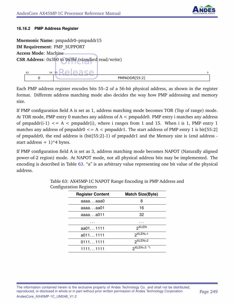
AndesCore AX45MP-1C Processor Reference Manual
16.16.2 PMP Address Register
Mnemonic Name: pmpaddr0–pmpaddr15IM Requirement: PMP_SUPPORTAccess Mode: MachineCSR Address: 0x3b0 to 0x3bf (standard read/write)
63 54
0
53 0
PMPADDR[55:2]
Each PMP address register encodes bits 55–2 of a 56-bit physical address, as shown in the registerformat. Different address matching mode also decides the way how PMP addressing and memorysize.
If PMP configuration field A is set as 1, address matching mode becomes TOR (Top of range) mode.At TOR mode, PMP entry 0 matches any address of A < pmpaddr0. PMP entry i matches any addressof pmpaddr(i-1) <= A < pmpaddr(i), where i ranges from 1 and 15. When i is 1, PMP entry 1matches any address of pmpaddr0 <= A < pmpaddr1. The start address of PMP entry 1 is bit[55:2]of pmpaddr0, the end address is (bit[55:2]-1) of pmpaddr1 and the Memory size is (end address -start address + 1)*4 bytes.
If PMP configuration field A is set as 3, address matching mode becomes NAPOT (Naturally alignedpower-of-2 region) mode. At NAPOT mode, not all physical address bits may be implemented. Theencoding is described in Table 63. “a” is an arbitrary value representing one bit value of the physicaladdress.
Table 63: AX45MP-1C NAPOT Range Encoding in PMP Address andConfiguration Registers
Register Content Match Size(Byte)
aaaa. . . aaa0 8
aaaa. . . aa01 16
aaaa. . . a011 32
. . . . . .
aa01. . . 1111 2XLEN
a011. . . 1111 2XLEN+1
0111. . . 1111 2XLEN+2
1111. . . 1111 2XLEN+3 *1
The information contained herein is the exclusive property of Andes Technology Co. and shall not be distributed,reproduced, or disclosed in whole or in part without prior written permission of Andes Technology Corporation.AndesCore_AX45MP-1C_UM248_V1.2
Page 249
AndesCore AX45MP-1C Processor Reference Manual
Note1. In Andes implementation, the behavior of this register content is the same as that of 0111. . . 1111 and
hence the match size is equivalent to 2XLEN+2.
The smallest PMP entry granularity is 8-bytes and pmpaddri[0] is hardwired to zero when the modeis OFF or TOR.
NoteWhen PMP is used in the cacheable memory space, a PMP region must also naturally align to the size of thecache line. Otherwise, a deliberate load to a cache line partially covered by a PMP region may bring the fullcache line to the Data Cache and allow CCTL operations to access the reset of the cache line that may havea different access restriction.
The information contained herein is the exclusive property of Andes Technology Co. and shall not be distributed,reproduced, or disclosed in whole or in part without prior written permission of Andes Technology Corporation.AndesCore_AX45MP-1C_UM248_V1.2
Page 250
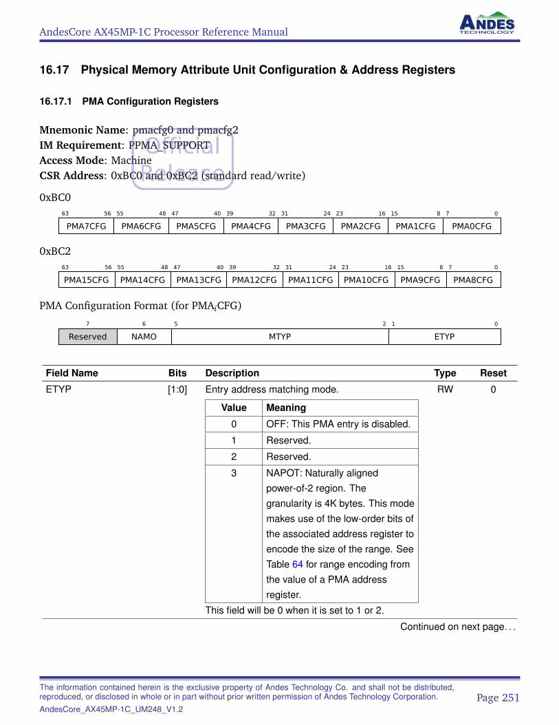
AndesCore AX45MP-1C Processor Reference Manual
16.17 Physical Memory Attribute Unit Configuration & Address Registers
16.17.1 PMA Configuration Registers
Mnemonic Name: pmacfg0 and pmacfg2IM Requirement: PPMA_SUPPORTAccess Mode: MachineCSR Address: 0xBC0 and 0xBC2 (standard read/write)
0xBC063 56
PMA7CFG
55 48
PMA6CFG
47 40
PMA5CFG
39 32
PMA4CFG
31 24
PMA3CFG
23 16
PMA2CFG
15 8
PMA1CFG
7 0
PMA0CFG
0xBC263 56
PMA15CFG
55 48
PMA14CFG
47 40
PMA13CFG
39 32
PMA12CFG
31 24
PMA11CFG
23 16
PMA10CFG
15 8
PMA9CFG
7 0
PMA8CFG
PMA Configuration Format (for PMAiCFG)
7
Reserved
6
NAMO
5 2
MTYP
1 0
ETYP
Field Name Bits Description Type Reset
ETYP [1:0] Entry address matching mode.
Value Meaning
0 OFF: This PMA entry is disabled.
1 Reserved.
2 Reserved.
3 NAPOT: Naturally alignedpower-of-2 region. Thegranularity is 4K bytes. This modemakes use of the low-order bits ofthe associated address register toencode the size of the range. SeeTable 64 for range encoding fromthe value of a PMA addressregister.
This field will be 0 when it is set to 1 or 2.
RW 0
Continued on next page. . .
The information contained herein is the exclusive property of Andes Technology Co. and shall not be distributed,reproduced, or disclosed in whole or in part without prior written permission of Andes Technology Corporation.AndesCore_AX45MP-1C_UM248_V1.2
Page 251
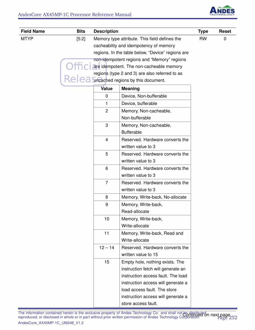
AndesCore AX45MP-1C Processor Reference Manual
Field Name Bits Description Type Reset
MTYP [5:2] Memory type attribute. This field defines thecacheability and idempotency of memoryregions. In the table below, “Device” regions arenon-idempotent regions and “Memory” regionsare idempotent. The non-cacheable memoryregions (type 2 and 3) are also referred to asuncached regions by this document.
Value Meaning
0 Device, Non-bufferable
1 Device, bufferable
2 Memory, Non-cacheable,Non-bufferable
3 Memory, Non-cacheable,Bufferable
4 Reserved. Hardware converts thewritten value to 3
5 Reserved. Hardware converts thewritten value to 3
6 Reserved. Hardware converts thewritten value to 3
7 Reserved. Hardware converts thewritten value to 3
8 Memory, Write-back, No-allocate
9 Memory, Write-back,Read-allocate
10 Memory, Write-back,Write-allocate
11 Memory, Write-back, Read andWrite-allocate
12 – 14 Reserved. Hardware converts thewritten value to 15
15 Empty hole, nothing exists. Theinstruction fetch will generate aninstruction access fault. The loadinstruction access will generate aload access fault. The storeinstruction access will generate astore access fault.
RW 0
Continued on next page. . .The information contained herein is the exclusive property of Andes Technology Co. and shall not be distributed,reproduced, or disclosed in whole or in part without prior written permission of Andes Technology Corporation.AndesCore_AX45MP-1C_UM248_V1.2
Page 252
AndesCore AX45MP-1C Processor Reference Manual
Field Name Bits Description Type Reset
NAMO [6] Indicate whether Atomic Memory Operationinstructions (including LR/SC) are not supportedin this region. When this bit is set and an AMOinstruction is encountered in this region, anaccess fault PMA NAMO exception will begenerated.
Value Meaning
0 AMO instructions (includingLR/SC) are supported in theregion.
1 AMO instructions (includingLR/SC) are not supported in theregion.
RW 0
The information contained herein is the exclusive property of Andes Technology Co. and shall not be distributed,reproduced, or disclosed in whole or in part without prior written permission of Andes Technology Corporation.AndesCore_AX45MP-1C_UM248_V1.2
Page 253
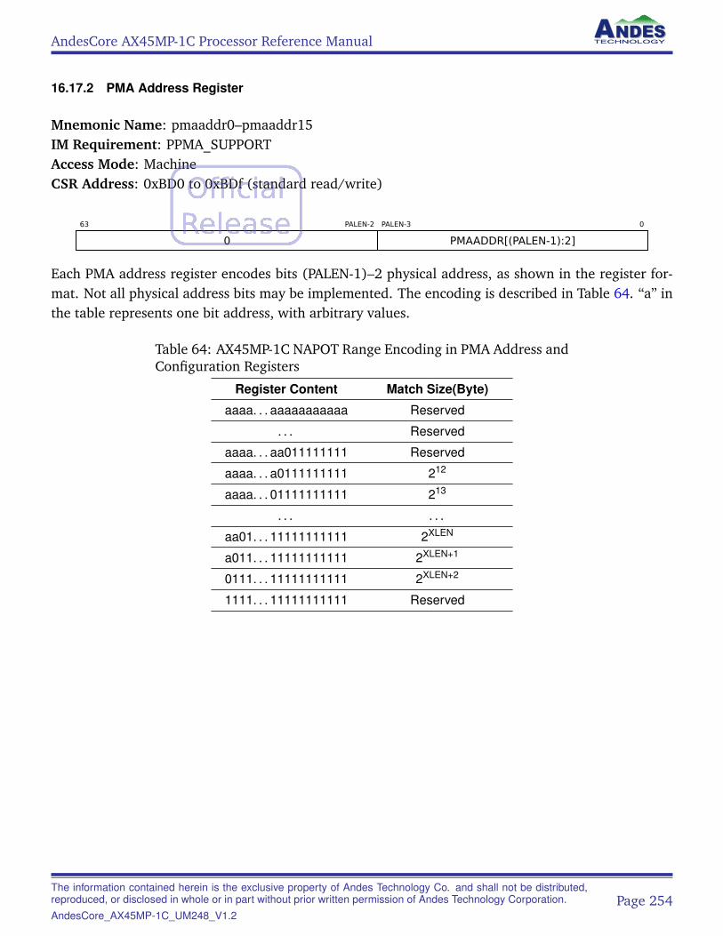
AndesCore AX45MP-1C Processor Reference Manual
16.17.2 PMA Address Register
Mnemonic Name: pmaaddr0–pmaaddr15IM Requirement: PPMA_SUPPORTAccess Mode: MachineCSR Address: 0xBD0 to 0xBDf (standard read/write)
63 PALEN-2
0
PALEN-3 0
PMAADDR[(PALEN-1):2]
Each PMA address register encodes bits (PALEN-1)–2 physical address, as shown in the register for-mat. Not all physical address bits may be implemented. The encoding is described in Table 64. “a” inthe table represents one bit address, with arbitrary values.
Table 64: AX45MP-1C NAPOT Range Encoding in PMA Address andConfiguration Registers
Register Content Match Size(Byte)
aaaa. . . aaaaaaaaaaa Reserved
. . . Reserved
aaaa. . . aa011111111 Reserved
aaaa. . . a0111111111 212
aaaa. . . 01111111111 213
. . . . . .
aa01. . . 11111111111 2XLEN
a011. . . 11111111111 2XLEN+1
0111. . . 11111111111 2XLEN+2
1111. . . 11111111111 Reserved
The information contained herein is the exclusive property of Andes Technology Co. and shall not be distributed,reproduced, or disclosed in whole or in part without prior written permission of Andes Technology Corporation.AndesCore_AX45MP-1C_UM248_V1.2
Page 254
AndesCore AX45MP-1C Processor Reference Manual
16.18 Floating-Point CSRs
16.18.1 Floating-Point Accrued Exception Flags
Mnemonic Name: fflagsIM Requirement: F or D ISA extension optionalAccess Mode: UserCSR Address: 0x001 (standard read/write)
63 5
0
4
NV
3
DZ
2
OF
1
UF
0
NX
Field Name Bits Description Type Reset
NX [0] Inexact exception flag RW 0
UF [1] Under flow exception flag RW 0
OF [2] Over flow exception flag RW 0
DZ [3] Divide by zero flag RW 0
NV [4] Invalid operation flag RW 0
This register is an aliased portion of the fcsr register.
16.18.2 Floating-Point Rounding Mode
Mnemonic Name: frmIM Requirement: F or D ISA extension optionalAccess Mode: UserCSR Address: 0x002 (standard read/write)
63 3
0
2 0
FRM
The information contained herein is the exclusive property of Andes Technology Co. and shall not be distributed,reproduced, or disclosed in whole or in part without prior written permission of Andes Technology Corporation.AndesCore_AX45MP-1C_UM248_V1.2
Page 255
AndesCore AX45MP-1C Processor Reference Manual
Field Name Bits Description Type Reset
FRM [2:0] Floating-point instruction dynamic round modecontrol:
Value Meaning
0 RNE: Round to nearest, ties toeven.
1 RTZ: Round towards zero.
2 RDN: Round down (towards -infinity)
3 RUP: Round up (towards +infinity)
4 RMM: Round to nearest, ties tomax magnitude
5 Reserved
6 Reserved
7 Reserved
RW 0
This register is an aliased portion of the fcsr register with the field position shifted to LSB.
16.18.3 Floating-Point Control and Status
Mnemonic Name: fcsrIM Requirement: F or D ISA extension optionalAccess Mode: UserCSR Address: 0x003 (standard read/write)
63 8
0
7 5
FRM
4
NV
3
DZ
2
OF
1
UF
0
NX
Field Name Bits Description Type Reset
NX [0] Inexact exception flag RW 0
UF [1] Under flow exception flag RW 0
OF [2] Over flow exception flag RW 0
DZ [3] Divide by zero flag RW 0
NV [4] Invalid operation flag RW 0
Continued on next page. . .
The information contained herein is the exclusive property of Andes Technology Co. and shall not be distributed,reproduced, or disclosed in whole or in part without prior written permission of Andes Technology Corporation.AndesCore_AX45MP-1C_UM248_V1.2
Page 256
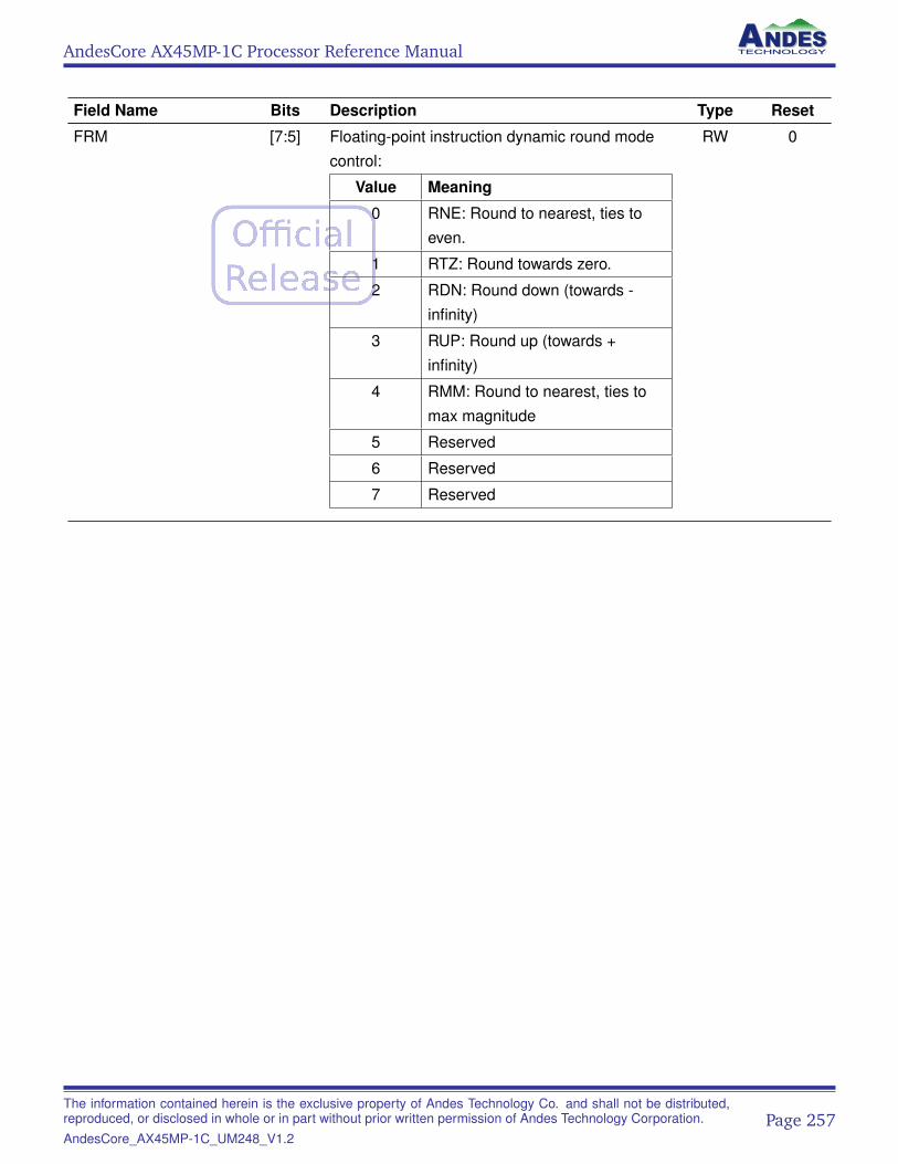
AndesCore AX45MP-1C Processor Reference Manual
Field Name Bits Description Type Reset
FRM [7:5] Floating-point instruction dynamic round modecontrol:
Value Meaning
0 RNE: Round to nearest, ties toeven.
1 RTZ: Round towards zero.
2 RDN: Round down (towards -infinity)
3 RUP: Round up (towards +infinity)
4 RMM: Round to nearest, ties tomax magnitude
5 Reserved
6 Reserved
7 Reserved
RW 0
The information contained herein is the exclusive property of Andes Technology Co. and shall not be distributed,reproduced, or disclosed in whole or in part without prior written permission of Andes Technology Corporation.AndesCore_AX45MP-1C_UM248_V1.2
Page 257
AndesCore AX45MP-1C Processor Reference Manual
16.19 User Counter Related CSRs
16.19.1 Cycle Counter
Mnemonic Name: cycleIM Requirement: misa.U==1Access Mode: UserCSR Address: 0xc00 (standard read only)
This register is the read-only shadow of mcycle register. Writing of this register in any mode willcause an illegal instruction exception (mcause==2). When the mcounteren.CY bit is cleared, at-tempts to read this register in User mode will cause an illegal instruction exception (mcause==2).
When mmsc_cfg.PMNDS==1, writing of this register in any mode is controlled by the mcounter
wen CSR. When the corresponding counter bit in mcounterwen is 0, writing of this register in anymode will cause an illegal instruction exception (mcause==2). When the corresponding counter bitin mcounterwen is 1, writing of this register in M-mode or S-mode is allowed for an M/S/U system.
The information contained herein is the exclusive property of Andes Technology Co. and shall not be distributed,reproduced, or disclosed in whole or in part without prior written permission of Andes Technology Corporation.AndesCore_AX45MP-1C_UM248_V1.2
Page 258
AndesCore AX45MP-1C Processor Reference Manual
16.19.2 User Time Register
Mnemonic Name: timeIM Requirement: misa.U==1Access Mode: UserCSR Address: 0xc01 (software emulation)
This is the register for RDTIME instruction. An implementation can trap the RDTIME instruction anduse a machine mode trap handler to get the timer value to emulate the correct behavior of a RDTIMEinstruction.
The information contained herein is the exclusive property of Andes Technology Co. and shall not be distributed,reproduced, or disclosed in whole or in part without prior written permission of Andes Technology Corporation.AndesCore_AX45MP-1C_UM248_V1.2
Page 259
AndesCore AX45MP-1C Processor Reference Manual
16.19.3 Instruction-Retired Counter
Mnemonic Name: instretIM Requirement: misa.U==1Access Mode: UserCSR Address: 0xc02 (standard read only)
This register is the read-only shadow of mcycle register. Writing of this register in any mode willcause an illegal instruction exception (mcause==2). When the mcounteren.CY bit is cleared, at-tempts to read this register in User mode will cause an illegal instruction exception (mcause==2).
When mmsc_cfg.PMNDS==1, writing of this register in any mode is controlled by the mcounter
wen CSR. When the corresponding counter bit in mcounterwen is 0, writing of this register in anymode will cause an illegal instruction exception (mcause==2). When the corresponding counter bitin mcounterwen is 1, writing of this register in M-mode or S-mode is allowed for an M/S/U system.
The information contained herein is the exclusive property of Andes Technology Co. and shall not be distributed,reproduced, or disclosed in whole or in part without prior written permission of Andes Technology Corporation.AndesCore_AX45MP-1C_UM248_V1.2
Page 260
AndesCore AX45MP-1C Processor Reference Manual
16.19.4 Performance Monitoring Counter
Mnemonic Name: hpmcounter3–hpmcounter6IM Requirement: misa.U==1Access Mode: UserCSR Address: 0xc03 to 0xc06 (standard read only)
These registers are the read-only shadow of mhpmcounter3-6 registers. Writing of these registersin any mode will cause an illegal instruction exception (mcause==2). When the mcounteren.
HPM3-6 bits are cleared, attempts to read these registers in User mode will cause an illegal instructionexception (mcause==2).
When mmsc_cfg.PMNDS==1, writing of this register in any mode is controlled by the mcounterwenCSR. When the corresponding counter bit in mcounterwen is 0, writing of this register in any modewill cause an illegal instruction exception (mcause==2). When the corresponding counter bit inmcounterwen is 1, writing of this register in M-mode or S-mode is allowed for an M/S/U system.
The information contained herein is the exclusive property of Andes Technology Co. and shall not be distributed,reproduced, or disclosed in whole or in part without prior written permission of Andes Technology Corporation.AndesCore_AX45MP-1C_UM248_V1.2
Page 261
AndesCore AX45MP-1C Processor Reference Manual
17 Instruction Throughput and Latency
This chapter lists instruction throughput and latency. The instruction throughput is the number ofcycles before executing the next independent instruction of the same kind. The instruction latency isthe number of cycles before executing the next instruction with read-after-write dependency.
17.1 ALU Instructions
The latency and the throughput of ALU instructions are both 1 cycle. ALU instructions include:
• Add/Sub: ADD, SUB, ADDI, ADDW, SUBW, ADDIW
• Shift: SLL, SRL, SRA, SLLI, SRLI, SRAI, SLLW, SRLW, SRAW, SLLIW, SRLIW, SRAIW
• Logical: AND, OR, XOR, ANDI, ORI, XORI
• Compare: SLT, SLTU, SLTI, SLTIU
• LUI and AUIPC
• Load effective address instructions
• ADDIGP
• String processing: FFB, FFZMISM, FFMISM, FLMISM
• Bit field operation: BFOS, BFOZ
17.2 Dual-Issue Capability
This section is only for CPU revision 10.0.0 and later. For earlier revisions, see earlier documents.
17.2.1 Dual-Issue Capability of Integer Instructions
AX45MP-1C can simultaneously execute two independent instructions. Table 65 shows dual-issuecapability of integer instruction pairs.
Table 65: Dual-Issue Capability
The First Instruction The Second Instruction Dual-Issue
ALU ALU Yes
Branch/Jump Yes
Continued on next page. . .
The information contained herein is the exclusive property of Andes Technology Co. and shall not be distributed,reproduced, or disclosed in whole or in part without prior written permission of Andes Technology Corporation.AndesCore_AX45MP-1C_UM248_V1.2
Page 262
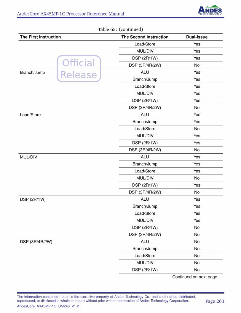
AndesCore AX45MP-1C Processor Reference Manual
Table 65: (continued)
The First Instruction The Second Instruction Dual-Issue
Load/Store Yes
MUL/DIV Yes
DSP (2R/1W) Yes
DSP (3R/4R/2W) No
Branch/Jump ALU Yes
Branch/Jump Yes
Load/Store Yes
MUL/DIV Yes
DSP (2R/1W) Yes
DSP (3R/4R/2W) No
Load/Store ALU Yes
Branch/Jump Yes
Load/Store No
MUL/DIV Yes
DSP (2R/1W) Yes
DSP (3R/4R/2W) No
MUL/DIV ALU Yes
Branch/Jump Yes
Load/Store Yes
MUL/DIV No
DSP (2R/1W) Yes
DSP (3R/4R/2W) No
DSP (2R/1W) ALU Yes
Branch/Jump Yes
Load/Store Yes
MUL/DIV Yes
DSP (2R/1W) No
DSP (3R/4R/2W) No
DSP (3R/4R/2W) ALU No
Branch/Jump No
Load/Store No
MUL/DIV No
DSP (2R/1W) No
Continued on next page. . .
The information contained herein is the exclusive property of Andes Technology Co. and shall not be distributed,reproduced, or disclosed in whole or in part without prior written permission of Andes Technology Corporation.AndesCore_AX45MP-1C_UM248_V1.2
Page 263
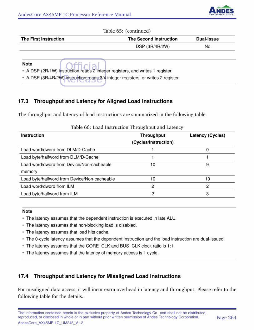
AndesCore AX45MP-1C Processor Reference Manual
Table 65: (continued)
The First Instruction The Second Instruction Dual-Issue
DSP (3R/4R/2W) No
Note• A DSP (2R/1W) instruction reads 2 integer registers, and writes 1 register.• A DSP (3R/4R/2W) instruction reads 3/4 integer registers, or writes 2 register.
17.3 Throughput and Latency for Aligned Load Instructions
The throughput and latency of load instructions are summarized in the following table.
Table 66: Load Instruction Throughput and Latency
Instruction Throughput(Cycles/Instruction)
Latency (Cycles)
Load word/dword from DLM/D-Cache 1 0
Load byte/halfword from DLM/D-Cache 1 1
Load word/dword from Device/Non-cacheablememory
10 9
Load byte/halfword from Device/Non-cacheable 10 10
Load word/dword from ILM 2 2
Load byte/halfword from ILM 2 3
Note• The latency assumes that the dependent instruction is executed in late ALU.• The latency assumes that non-blocking load is disabled.• The latency assumes that load hits cache.• The 0-cycle latency assumes that the dependent instruction and the load instruction are dual-issued.• The latency assumes that the CORE_CLK and BUS_CLK clock ratio is 1:1.• The latency assumes that the latency of memory access is 1 cycle.
17.4 Throughput and Latency for Misaligned Load Instructions
For misaligned data access, it will incur extra overhead in latency and throughput. Please refer to thefollowing table for the details.
The information contained herein is the exclusive property of Andes Technology Co. and shall not be distributed,reproduced, or disclosed in whole or in part without prior written permission of Andes Technology Corporation.AndesCore_AX45MP-1C_UM248_V1.2
Page 264
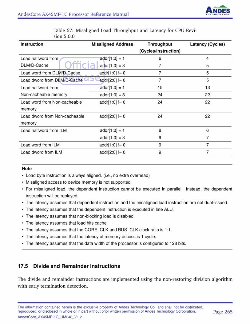
AndesCore AX45MP-1C Processor Reference Manual
Table 67: Misaligned Load Throughput and Latency for CPU Revi-sion 5.0.0
Instruction Misaligned Address Throughput(Cycles/Instruction)
Latency (Cycles)
Load halfword fromDLM/D-Cache
addr[1:0] = 1 6 4
addr[1:0] = 3 7 5
Load word from DLM/D-Cache addr[1:0] != 0 7 5
Load dword from DLM/D-Cache addr[2:0] != 0 7 5
Load halfword fromNon-cacheable memory
addr[1:0] = 1 15 13
addr[1:0] = 3 24 22
Load word from Non-cacheablememory
addr[1:0] != 0 24 22
Load dword from Non-cacheablememory
addr[2:0] != 0 24 22
Load halfword from ILM addr[1:0] = 1 8 6
addr[1:0] = 3 9 7
Load word from ILM addr[1:0] != 0 9 7
Load dword from ILM addr[2:0] != 0 9 7
Note• Load byte instruction is always aligned. (i.e., no extra overhead)• Misaligned access to device memory is not supported.• For misaligned load, the dependent instruction cannot be executed in parallel. Instead, the dependent
instruction will be replayed.• The latency assumes that dependent instruction and the misaligned load instruction are not dual-issued.• The latency assumes that the dependent instruction is executed in late ALU.• The latency assumes that non-blocking load is disabled.• The latency assumes that load hits cache.• The latency assumes that the CORE_CLK and BUS_CLK clock ratio is 1:1.• The latency assumes that the latency of memory access is 1 cycle.• The latency assumes that the data width of the processor is configured to 128 bits.
17.5 Divide and Remainder Instructions
The divide and remainder instructions are implemented using the non-restoring division algorithmwith early termination detection.
The information contained herein is the exclusive property of Andes Technology Co. and shall not be distributed,reproduced, or disclosed in whole or in part without prior written permission of Andes Technology Corporation.AndesCore_AX45MP-1C_UM248_V1.2
Page 265
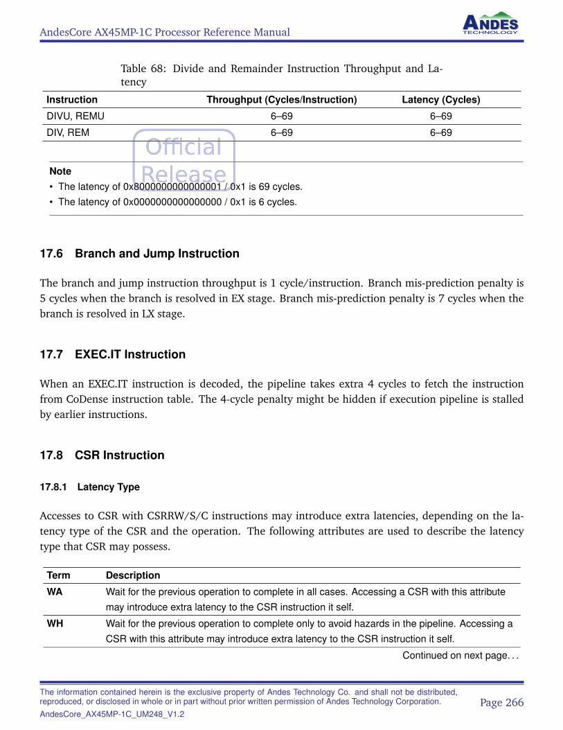
AndesCore AX45MP-1C Processor Reference Manual
Table 68: Divide and Remainder Instruction Throughput and La-tency
Instruction Throughput (Cycles/Instruction) Latency (Cycles)
DIVU, REMU 6–69 6–69
DIV, REM 6–69 6–69
Note• The latency of 0x8000000000000001 / 0x1 is 69 cycles.• The latency of 0x0000000000000000 / 0x1 is 6 cycles.
17.6 Branch and Jump Instruction
The branch and jump instruction throughput is 1 cycle/instruction. Branch mis-prediction penalty is5 cycles when the branch is resolved in EX stage. Branch mis-prediction penalty is 7 cycles when thebranch is resolved in LX stage.
17.7 EXEC.IT Instruction
When an EXEC.IT instruction is decoded, the pipeline takes extra 4 cycles to fetch the instructionfrom CoDense instruction table. The 4-cycle penalty might be hidden if execution pipeline is stalledby earlier instructions.
17.8 CSR Instruction
17.8.1 Latency Type
Accesses to CSR with CSRRW/S/C instructions may introduce extra latencies, depending on the la-tency type of the CSR and the operation. The following attributes are used to describe the latencytype that CSR may possess.
Term Description
WA Wait for the previous operation to complete in all cases. Accessing a CSR with this attributemay introduce extra latency to the CSR instruction it self.
WH Wait for the previous operation to complete only to avoid hazards in the pipeline. Accessing aCSR with this attribute may introduce extra latency to the CSR instruction it self.
Continued on next page. . .
The information contained herein is the exclusive property of Andes Technology Co. and shall not be distributed,reproduced, or disclosed in whole or in part without prior written permission of Andes Technology Corporation.AndesCore_AX45MP-1C_UM248_V1.2
Page 266
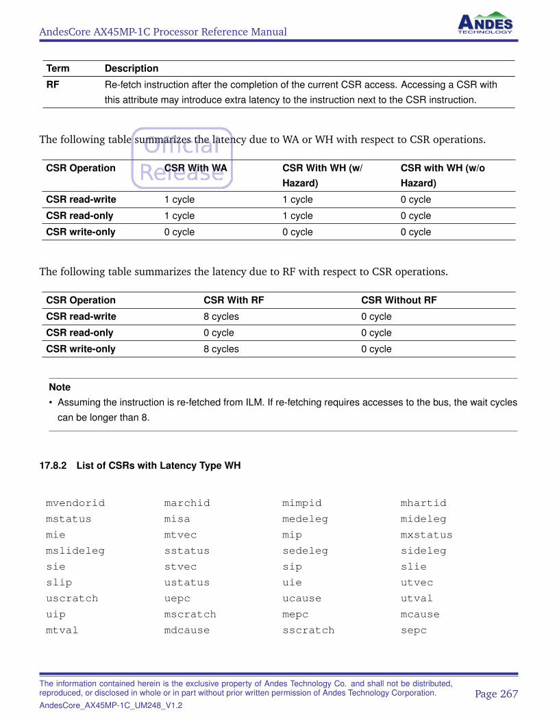
AndesCore AX45MP-1C Processor Reference Manual
Term Description
RF Re-fetch instruction after the completion of the current CSR access. Accessing a CSR withthis attribute may introduce extra latency to the instruction next to the CSR instruction.
The following table summarizes the latency due to WA or WH with respect to CSR operations.
CSR Operation CSR With WA CSR With WH (w/Hazard)
CSR with WH (w/oHazard)
CSR read-write 1 cycle 1 cycle 0 cycle
CSR read-only 1 cycle 1 cycle 0 cycle
CSR write-only 0 cycle 0 cycle 0 cycle
The following table summarizes the latency due to RF with respect to CSR operations.
CSR Operation CSR With RF CSR Without RF
CSR read-write 8 cycles 0 cycle
CSR read-only 0 cycle 0 cycle
CSR write-only 8 cycles 0 cycle
Note• Assuming the instruction is re-fetched from ILM. If re-fetching requires accesses to the bus, the wait cycles
can be longer than 8.
17.8.2 List of CSRs with Latency Type WH
mvendorid marchid mimpid mhartid
mstatus misa medeleg mideleg
mie mtvec mip mxstatus
mslideleg sstatus sedeleg sideleg
sie stvec sip slie
slip ustatus uie utvec
uscratch uepc ucause utval
uip mscratch mepc mcause
mtval mdcause sscratch sepc
The information contained herein is the exclusive property of Andes Technology Co. and shall not be distributed,reproduced, or disclosed in whole or in part without prior written permission of Andes Technology Corporation.AndesCore_AX45MP-1C_UM248_V1.2
Page 267
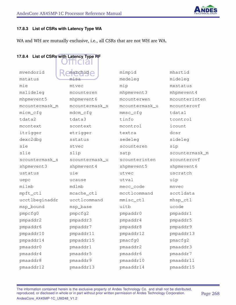
AndesCore AX45MP-1C Processor Reference Manual
17.8.3 List of CSRs with Latency Type WA
WA and WH are mutually exclusive, i.e., all CSRs that are not WH are WA.
17.8.4 List of CSRs with Latency Type RF
mvendorid marchid mimpid mhartid
mstatus misa medeleg mideleg
mie mtvec mip mxstatus
mslideleg mcounteren mhpmevent3 mhpmevent4
mhpmevent5 mhpmevent6 mcounterwen mcounterinten
mcountermask_m mcountermask_s mcountermask_u mcounterovf
micm_cfg mdcm_cfg mmsc_cfg tdata1
tdata2 tdata3 tinfo tcontrol
mcontext scontext mcontrol icount
itrigger etrigger textra dcsr
dexc2dbg sstatus sedeleg sideleg
sie stvec scounteren sip
slie slip satp scountermask_m
scountermask_s scountermask_u scounterinten scounterovf
shpmevent3 shpmevent4 shpmevent5 shpmevent6
ustatus uie utvec uscratch
uepc ucause utval uip
milmb mdlmb mecc_code mnvec
mpft_ctl mcache_ctl mcctlcommand scctldata
ucctlbeginaddr ucctlcommand mmisc_ctl mhsp_ctl
msp_bound msp_base uitb ucode
pmpcfg0 pmpcfg2 pmpaddr0 pmpaddr1
pmpaddr2 pmpaddr3 pmpaddr4 pmpaddr5
pmpaddr6 pmpaddr7 pmpaddr8 pmpaddr9
pmpaddr10 pmpaddr11 pmpaddr12 pmpaddr13
pmpaddr14 pmpaddr15 pmacfg0 pmacfg2
pmaaddr0 pmaaddr1 pmaaddr2 pmaaddr3
pmaaddr4 pmaaddr5 pmaaddr6 pmaaddr7
pmaaddr8 pmaaddr9 pmaaddr10 pmaaddr11
pmaaddr12 pmaaddr13 pmaaddr14 pmaaddr15
The information contained herein is the exclusive property of Andes Technology Co. and shall not be distributed,reproduced, or disclosed in whole or in part without prior written permission of Andes Technology Corporation.AndesCore_AX45MP-1C_UM248_V1.2
Page 268
AndesCore AX45MP-1C Processor Reference Manual
17.9 Trap Return Instruction
The trap return instruction flushes the entire pipeline, and the penalty is 8 cycles.
17.10 FENCE Instruction
FENCE instruction flushes the entire pipeline and waits for outstanding memory access. The penaltyis 13 cycles if there is no outstanding memory access.
17.11 Scalar Floating-Point Instructions for CPU Revision 10.0.0 and Later
The instruction latencies of floating-point instruction groups are shown in the following table.
Table 69: Scalar Floating-Point Instruction Throughput and Latencyfor CPU Revision 10.0.0 and Later Revisions
Instruction Throughput(Cycles/Instruction)
Latency (Cycles)
FADD.x, FSUB.x, FMUL.x, FMADD.x, FMSUB.x,FNMADD.x FNMSUB.x
1 3/4 (Note)
FDIV.D, FSQRT.D 32 33
FDIV.S, FSQRT.S 18 19
FDIV.H, FSQRT.H 11 12
FLH, FLW, FLD 2 4
FSGNJ.x, FSGNJN.x, FSGNJX.x, FMIN.x, FMAX.x 1 2
FCLASS.x, FEQ.x, FLT.x, FLE.x 1 10
FCVT.D.x, FCVT.S.x, FCVT.H.x, FCVT.BF16.x 1 2
FCVT.L.x, FCVT.LU.x, FCVT.W.x, FCVT.WU.x 1 10
FMV.D.X, FMV.W.X, FMV.H.X 1 2
FMV.X.D, FMV.X.W, FMV.X.H 1 10
Note• The latency is 4 for floating-point add, subtract, multiplier and MAC operations when double precision FPU
is configured.• The latency is 3 for floating-point add, subtract, multiplier and MAC operations when single precision FPU
is configured.
The information contained herein is the exclusive property of Andes Technology Co. and shall not be distributed,reproduced, or disclosed in whole or in part without prior written permission of Andes Technology Corporation.AndesCore_AX45MP-1C_UM248_V1.2
Page 269
AndesCore AX45MP-1C Processor Reference Manual
17.12 DSP Instructions
The instruction latencies of DSP instruction groups are shown in the following tables.
DSP instructions include:
• Non-MUL Arithmetic Operation (8/16/32/64-bit): ADD8, SUB16, CLZ32, RSUB64, . . .
• MUL8*8: KHM8, . . .
• MUL8*8 with 32-bit ADD/SUB: SMAQA, . . .
• MUL16*16: KHM16, . . .
• MUL16*16 with 32-bit ADD/SUB: KMDA, . . .
• MUL16*16 with 64-bit ADD/SUB: SMAL, . . .
• MUL32*32: SMMUL, . . .
• MUL32*32 with 32-bit ADD/SUB: KMMAC, . . .
• MUL32*32 with 64-bit ADD/SUB: KMAR64, . . .
• MUL32*16: SMMWB, . . .
• MUL32*16 with 32-bit ADD/SUB: KMMAWB, . . .
Table 70: DSP Instruction Throughput and Latency
Instruction Throughput (Cy-cles/Instruction)
Latency (Cycles)
Non-MUL Arithmetic Operation 1 1
MUL8*8 1 1
MUL8*8 with 32-bit ADD/SUB 1 2
MUL16*16 1 2
MUL16*16 with 32-bit ADD/SUB 1 2
MUL16*16 with 64-bit ADD/SUB 1 3
MUL32*32 1 2
MUL32*32 with 32-bit ADD/SUB 1 2
MUL32*32 with 64-bit ADD/SUB 1 3
MUL32*16 1 2
MUL32*16 with 32-bit ADD/SUB 1 2
The information contained herein is the exclusive property of Andes Technology Co. and shall not be distributed,reproduced, or disclosed in whole or in part without prior written permission of Andes Technology Corporation.AndesCore_AX45MP-1C_UM248_V1.2
Page 270
AndesCore AX45MP-1C Processor Reference Manual
18 Platform-Level Interrupt Controller (PLIC)
18.1 Introduction
Andes Platform-Level Interrupt Controller (NCEPLIC100) prioritizes and distributes global interrupts.It is compatible with RISC-V PLIC with the following features:
• Configurable interrupt trigger types• Software-programmable interrupt generation• Preemptive priority interrupt extension• Vectored interrupt extension
See Section 18.2 for information regarding the Andes preemptive priority interrupt extension andSection 18.3 for information regarding the Andes vectored PLIC extension.
The block diagram of NCEPLIC100 is shown in Figure 3. Interrupt sources are connected to theinterrupt gateway of the PLIC controller, at which they are converted to interrupt requests. Interruptrequests are prioritized and routed to interrupt targets (e.g., AndesCore processor cores) according tointerrupt settings. Interrupt settings include enable bits, priorities, and priority thresholds, and thesesettings are programmable through the bus interface. Note that interrupt targets should not modifyenable bits, priorities and priority thresholds if there are any un-serviced interrupts.
When a target takes the external interrupt, it should send an interrupt claim request (bus read request)to retrieve the interrupt ID, upon which the corresponding interrupt pending status bit will be cleared.
The interrupt gateway stops processing newer interrupt requests from its interrupt sources once itreports an interrupt request. When the target has serviced the interrupt, it should send the interruptcompletion message (bus write request) to NCEPLIC100 such that the interrupt gateway resumesprocessing newer interrupt requests.
The interrupt pending bit array of the PLIC registers provides a summary of all interrupt sources sta-tus. In addition, it is also writable for setting software-programmed interrupts for the correspondinginterrupt sources. See Section 18.4.4 for more information.
The information contained herein is the exclusive property of Andes Technology Co. and shall not be distributed,reproduced, or disclosed in whole or in part without prior written permission of Andes Technology Corporation.AndesCore_AX45MP-1C_UM248_V1.2
Page 271
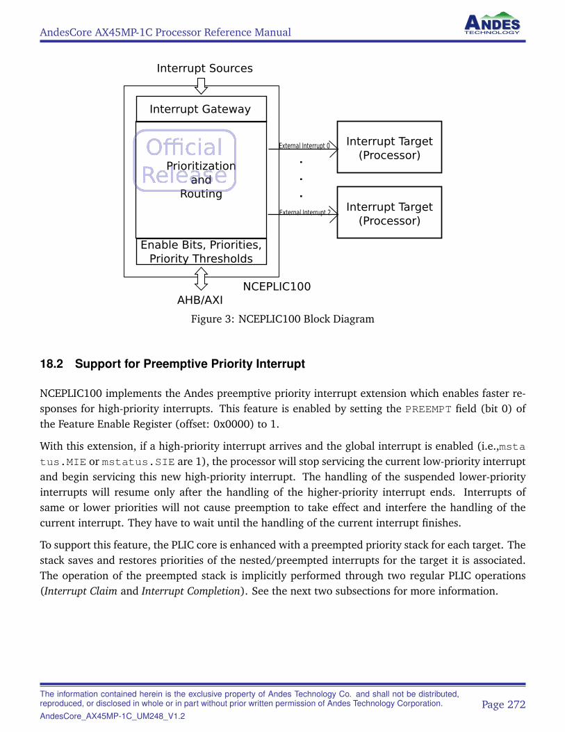
AndesCore AX45MP-1C Processor Reference Manual
NCEPLIC100AHB/AXI
Interrupt Target(Processor)
External Interrupt 0
Interrupt Target(Processor)
Interrupt Sources
Interrupt Gateway
Prioritizationand
Routing
Enable Bits, Priorities,Priority Thresholds
External Interrupt 2
.
.
.
Figure 3: NCEPLIC100 Block Diagram
18.2 Support for Preemptive Priority Interrupt
NCEPLIC100 implements the Andes preemptive priority interrupt extension which enables faster re-sponses for high-priority interrupts. This feature is enabled by setting the PREEMPT field (bit 0) ofthe Feature Enable Register (offset: 0x0000) to 1.
With this extension, if a high-priority interrupt arrives and the global interrupt is enabled (i.e.,mstatus.MIE or mstatus.SIE are 1), the processor will stop servicing the current low-priority interruptand begin servicing this new high-priority interrupt. The handling of the suspended lower-priorityinterrupts will resume only after the handling of the higher-priority interrupt ends. Interrupts ofsame or lower priorities will not cause preemption to take effect and interfere the handling of thecurrent interrupt. They have to wait until the handling of the current interrupt finishes.
To support this feature, the PLIC core is enhanced with a preempted priority stack for each target. Thestack saves and restores priorities of the nested/preempted interrupts for the target it is associated.The operation of the preempted stack is implicitly performed through two regular PLIC operations(Interrupt Claim and Interrupt Completion). See the next two subsections for more information.
The information contained herein is the exclusive property of Andes Technology Co. and shall not be distributed,reproduced, or disclosed in whole or in part without prior written permission of Andes Technology Corporation.AndesCore_AX45MP-1C_UM248_V1.2
Page 272
AndesCore AX45MP-1C Processor Reference Manual
18.2.1 Interrupt Claims with Preemptive Priority
When a target sends an interrupt claim message to the PLIC core, the PLIC core will atomicallydetermine the ID of the highest-priority pending interrupt for the target and then deassert the corre-sponding source’s IP bit. The PLIC core will then return the ID to the target.
At the same time, the priority number in the target’s Priority Threshold Register will be saved to apreempted priority stack for that target and the new priority number of the claimed interrupt will bewritten to the Priority Threshold Register.
18.2.2 Interrupt Completion with Preemptive Priority
When a target sends an interrupt completion message to the PLIC core, in addition to forwarding thecompletion message to the associated gateway, the PLIC core will restore the highest priority numberin the preempted priority stack back to the Priority Threshold Register of the target.
Note that out-of-order completion of interrupts is not allowed when this feature is turned on — thelatest claimed interrupt should be completed first.
18.2.3 Programming Sequence to Allow Preemption of Interrupts
Turning on the global interrupt enable flag (mstatus.MIE or mstatus.SIE) is all it takes to allowthe current interrupt handler to be preempted by higher priority interrupts. However, as the pre-emptive priority stack operations do not allow out-of-order completion, some care should be taken tomake sure that the claim and completion operations are nested properly.
For the non-vectored mode single-entry interrupt handler, the global interrupt enable flag could beturned on after the processor context are saved and Interrupt Claim is performed to allow preemptionof the current interrupt handler. At the end of interrupt handler, an Interrupt Completion message isperformed to signal that the handler has processed the interrupt and PLIC may deliver the next inter-rupt from the same interrupt source again. As both claim and completion messages are done throughload/store instructions to device regions, they should automatically be ordered correctly. Comparedwith the vectored mode interrupt handler two paragraphs below, the global interrupt flag does notneed to be disabled and no FENCE needs to be inserted after sending the completion message.
In summary, below is the suggested sequence for a non-vector mode interrupt handler for supportingpreemptive priority interrupts:
1. Save registers/CSRs to stack
2. Sends Interrupt Claim message to PLIC (device-load)
3. Enable global interrupt (mstatus.MIE/SIE)
The information contained herein is the exclusive property of Andes Technology Co. and shall not be distributed,reproduced, or disclosed in whole or in part without prior written permission of Andes Technology Corporation.AndesCore_AX45MP-1C_UM248_V1.2
Page 273
AndesCore AX45MP-1C Processor Reference Manual
4. Handle the expected interrupt
5. Sends Interrupt Completion message to PLIC (device-store)
6. Restore registers/CSRs
7. Return from interrupt
For vector mode interrupt handlers (see the next section), Interrupt Claim is implicit when the externalinterrupt is taken. The global interrupt enable flag could be turned on as long as the processorcontext are saved to allow preemption of the current interrupt handler. However, the global interruptflag should be turned off before Interrupt Completion operations are performed, since the processorwill trigger the next implicit Interrupt Claim operation as soon as the global interrupt enable flag isturned on and cause races between Interrupt Claim and Interrupt Completion. Additionally, a FENCEio,io operation should be inserted after the Interrupt Completion operation to make sure that thecompletion message reaches PLIC before the interrupt handler returns, which turns on the interruptenable flag again and cause the next Interrupt Claim to be performed.
In summary, below is the suggested sequence for a vector mode interrupt handler for supportingpreemptive priority interrupts:
1. Save registers/CSRs to stack
2. Enable global interrupt (mstatus.MIE/SIE)
3. Handle the expected interrupt
4. Disable global interrupt (mstatus.MIE/SIE)
5. Sends Interrupt Completion message to PLIC (device-store)
6. Restore registers/CSRs
7. Use a FENCE io,io instruction to ensure that the completion message has reached PLIC.
8. Return from interrupt
18.3 Vectored Interrupts
NCEPLIC100 enhances the RISC-V PLIC functionality with the vector mode extension to allow theinterrupt target to receive the interrupt source ID without going through the target claim requestprotocol. This feature can shorten the latency of interrupt handling by enabling the interrupt targetto run the corresponding interrupt handler directly upon accepting the external interrupt. It is enabledby setting the VECTORED field of the Feature Enable Register (offset: 0x0000) to 1.
The information contained herein is the exclusive property of Andes Technology Co. and shall not be distributed,reproduced, or disclosed in whole or in part without prior written permission of Andes Technology Corporation.AndesCore_AX45MP-1C_UM248_V1.2
Page 274
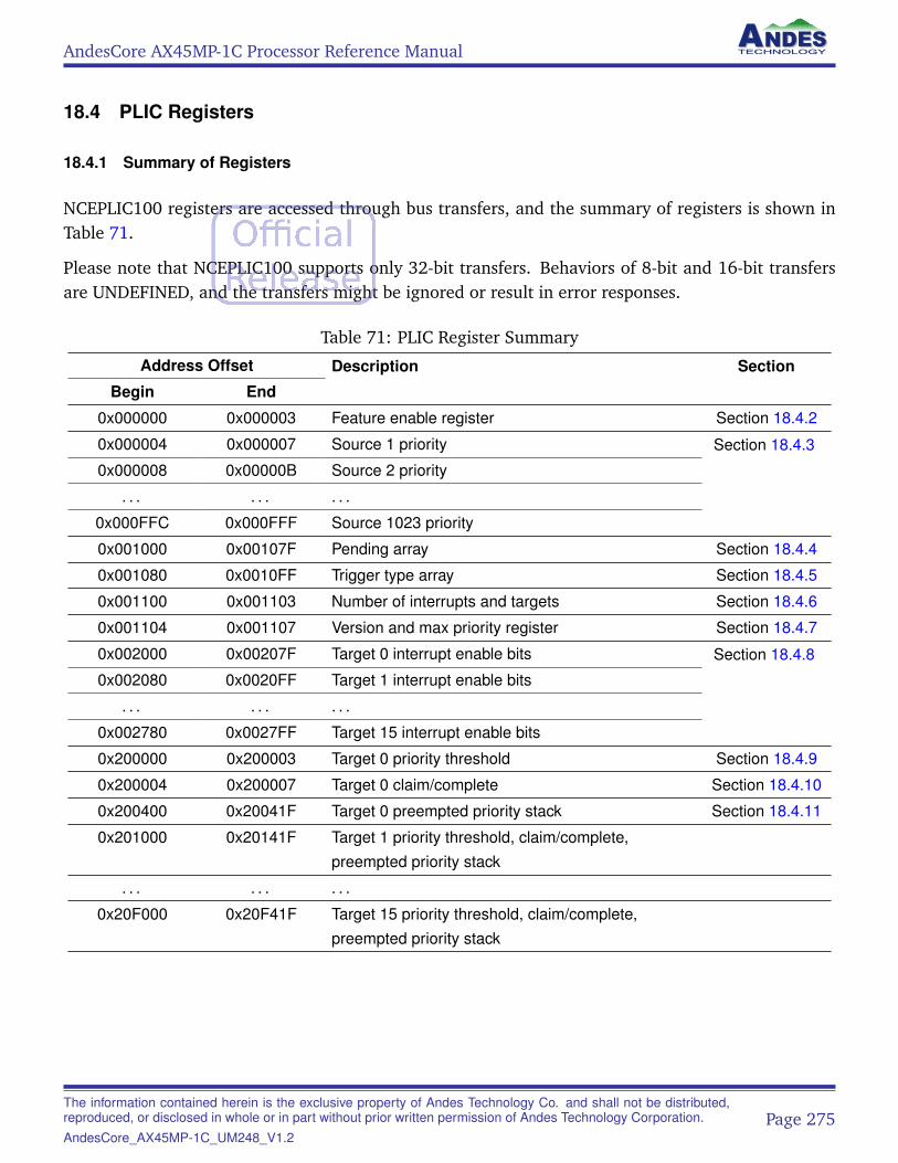
AndesCore AX45MP-1C Processor Reference Manual
18.4 PLIC Registers
18.4.1 Summary of Registers
NCEPLIC100 registers are accessed through bus transfers, and the summary of registers is shown inTable 71.
Please note that NCEPLIC100 supports only 32-bit transfers. Behaviors of 8-bit and 16-bit transfersare UNDEFINED, and the transfers might be ignored or result in error responses.
Table 71: PLIC Register Summary
Address Offset Description Section
Begin End
0x000000 0x000003 Feature enable register Section 18.4.2
0x000004 0x000007 Source 1 priority Section 18.4.3
0x000008 0x00000B Source 2 priority
. . . . . . . . .
0x000FFC 0x000FFF Source 1023 priority
0x001000 0x00107F Pending array Section 18.4.4
0x001080 0x0010FF Trigger type array Section 18.4.5
0x001100 0x001103 Number of interrupts and targets Section 18.4.6
0x001104 0x001107 Version and max priority register Section 18.4.7
0x002000 0x00207F Target 0 interrupt enable bits Section 18.4.8
0x002080 0x0020FF Target 1 interrupt enable bits
. . . . . . . . .
0x002780 0x0027FF Target 15 interrupt enable bits
0x200000 0x200003 Target 0 priority threshold Section 18.4.9
0x200004 0x200007 Target 0 claim/complete Section 18.4.10
0x200400 0x20041F Target 0 preempted priority stack Section 18.4.11
0x201000 0x20141F Target 1 priority threshold, claim/complete,preempted priority stack
. . . . . . . . .
0x20F000 0x20F41F Target 15 priority threshold, claim/complete,preempted priority stack
The information contained herein is the exclusive property of Andes Technology Co. and shall not be distributed,reproduced, or disclosed in whole or in part without prior written permission of Andes Technology Corporation.AndesCore_AX45MP-1C_UM248_V1.2
Page 275
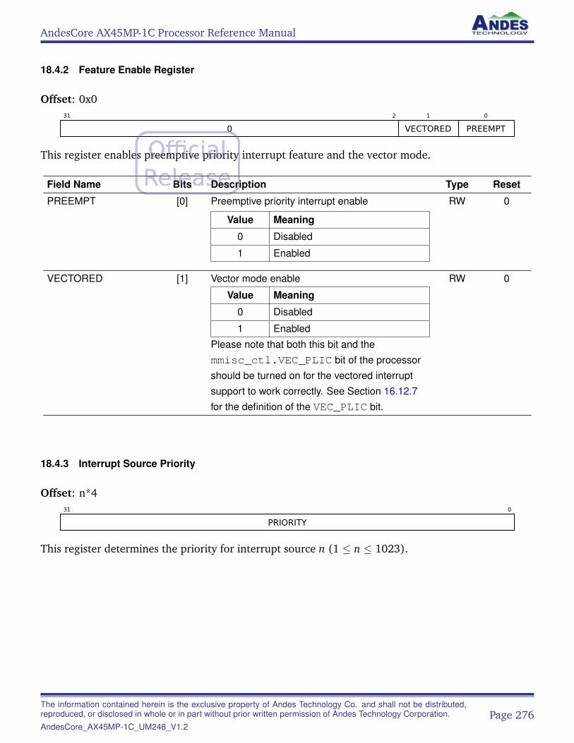
AndesCore AX45MP-1C Processor Reference Manual
18.4.2 Feature Enable Register
Offset: 0x031 2
0
1
VECTORED
0
PREEMPT
This register enables preemptive priority interrupt feature and the vector mode.
Field Name Bits Description Type Reset
PREEMPT [0] Preemptive priority interrupt enable
Value Meaning
0 Disabled
1 Enabled
RW 0
VECTORED [1] Vector mode enable
Value Meaning
0 Disabled
1 Enabled
Please note that both this bit and themmisc_ctl.VEC_PLIC bit of the processorshould be turned on for the vectored interruptsupport to work correctly. See Section 16.12.7for the definition of the VEC_PLIC bit.
RW 0
18.4.3 Interrupt Source Priority
Offset: n*431 0
PRIORITY
This register determines the priority for interrupt source n (1 ≤ n ≤ 1023).
The information contained herein is the exclusive property of Andes Technology Co. and shall not be distributed,reproduced, or disclosed in whole or in part without prior written permission of Andes Technology Corporation.AndesCore_AX45MP-1C_UM248_V1.2
Page 276
AndesCore AX45MP-1C Processor Reference Manual
Field Name Bits Description Type Reset
PRIORITY [31:0] Interrupt source priority. The valid range of thisfield is determined by the MAX_PRIORITY fieldof the Version & Maximum Priority ConfigurationRegister.
Value Meaning
0 Never interrupt.
1–255 Interrupt source priority. Thelarger the value, the higher thepriority.
RW 1
18.4.4 Interrupt Pending
Offset: 0x1000 to 0x107F
These registers provide the interrupt pending status of interrupt sources, and a way for software totrigger an interrupt without relying on external devices. Every interrupt source occupies 1 bit. Thereare a total of 32 registers, each 32-bit wide, for 1023 interrupt sources. Note that zero is not a validinterrupt source number so bit 0 of the first register is hardwired to 0.
When these registers are read, the interrupt pending status of interrupt sources are returned. Thepending bits could be set by writing a bit mask that specifies the bit positions to be set, and this actionwould result in software-programmed interrupts of the corresponding interrupt sources. The pendingbits could only be cleared through the Interrupt Claim requests.
The location of the interrupt pending bit for interrupt source n (1 ≤ n ≤ 1023) can be determined bythe following equations:
• Word offset address: 0x1000 + 4 * floor(n/32)
• Bit Position: n modulo 32
18.4.5 Interrupt Trigger Type
Offset: 0x1080 to 0x10FF
These registers are read-only and indicate the configured interrupt trigger type of interrupt sources.Every interrupt source occupies 1 bit. There are a total of 32 registers, each 32-bit wide, for 1023interrupt sources. The location of the interrupt trigger type bit for interrupt source n (1 ≤ n ≤ 1023)can be determined by the following equations:
The information contained herein is the exclusive property of Andes Technology Co. and shall not be distributed,reproduced, or disclosed in whole or in part without prior written permission of Andes Technology Corporation.AndesCore_AX45MP-1C_UM248_V1.2
Page 277
AndesCore AX45MP-1C Processor Reference Manual
• Word offset address: 0x1080 + 4 * floor(n/32)
• Bit Position: n modulo 32
The meaning of each bit is shown in Table 72. Note that zero is not a valid interrupt source numberso bit 0 of the first register is hardwired to 0.
Table 72: Meaning of Trigger Type
Value Meaning
0 Level-triggered interrupt
1 Edge-triggered interrupt
18.4.6 Number of Interrupt and Target Configuration Register
Offset: 0x110031 16
NUM_TARGET
15 0
NUM_INTERRUPT
This register indicates the number of supported interrupt sources and supported targets.
Field Name Bits Description Type Reset
NUM_INTERRUPT [15:0] The number of supported interrupt sources RO IM
NUM_TARGET [31:16] The number of supported targets RO IM
18.4.7 Version & Maximum Priority Configuration Register
Offset: 0x110431 16
MAX_PRIORITY
15 0
VERSION
This register indicates the version and the maximum priority of PLIC implementation.
Field Name Bits Description Type Reset
VERSION [15:0] The version of the PLIC design RO IM
MAX_PRIORITY [31:16] The maximum priority supported RO IM
The information contained herein is the exclusive property of Andes Technology Co. and shall not be distributed,reproduced, or disclosed in whole or in part without prior written permission of Andes Technology Corporation.AndesCore_AX45MP-1C_UM248_V1.2
Page 278
AndesCore AX45MP-1C Processor Reference Manual
18.4.8 Interrupt Enable Bits for Target m
Offset: (0x2000+m*128) to (0x207F+m*128)
These registers control the routing of interrupt source n to target m (1 ≤ n ≤ 1023 and m ≥ 0).Each bit controls one interrupt source. For each target, there are a total of 32 word-sized registersfor controlling 1023 interrupt sources to that target. Note that zero is not a valid interrupt sourcenumber so bit 0 of the first register is hardwired to 0.
The location of the interrupt enable bit for interrupt source n to target m can be determined by thefollowing equations:
• Word offset address: 0x2000 + 128 * m + 4 * floor(n/32)
• Bit position: n modulo 32
The following pseudo code demonstrates how to enable interrupt n for target m:
intptr_t reg_offset = 0x2000 + 128 * m + 4 * (n/32);
int bit_position = n % 32;
volatile uint32_t *reg_pointer = (volatile uint32_t *)(PLIC_BASE+reg_offset);
*reg_pointer = *reg_pointer | (1 << bit_position);
18.4.9 Priority Threshold for Target m
Offset: 0x200000+4096*m31 0
THRESHOLD
Each interrupt target m (m ≥ 0) is associated with one Priority Threshold Register. Only activeinterrupts with priorities strictly greater than the threshold will cause an interrupt notification to besent to the target.
Field Name Bits Description Type Reset
THRESHOLD [31:0] Interrupt priority threshold. The valid range ofthis field is determined by the MAX_PRIORITYfield of the Version & Maximum PriorityConfiguration Register.
RW 0
The information contained herein is the exclusive property of Andes Technology Co. and shall not be distributed,reproduced, or disclosed in whole or in part without prior written permission of Andes Technology Corporation.AndesCore_AX45MP-1C_UM248_V1.2
Page 279
AndesCore AX45MP-1C Processor Reference Manual
18.4.10 Claim and Complete Register for Target m
Offset: 0x200004+4096*m31 10
0
9 0
INTERRUPT_ID
There is one Claim and Complete Register for each interrupt target m (m ≥ 0). Reading this registerclaims an interrupt source and returns the ID of that interrupt source.
The interrupt gateway stops processing newer interrupt requests from its interrupt sources until theearlier interrupt request completes. Writing this register with an interrupt ID serves as the inter-rupt completion message acknowledging to PLIC that the handling of the claimed interrupt has beenserviced in target m and the associated interrupt gateway may resume processing newer interruptrequests.
The interrupt gateway only resumes processing of newer interrupt requests if the enable bit of theinterrupt source for target m is set. If the enable bit is not set, the interrupt completion message willbe ignored.
Generally there are no limitations to the order of interrupt claims and completions except when thepreemptive priority mode is enabled. When PLIC is in the preemptive priority mode, the latest claimedinterrupt should be completed first.
Field Name Bits Description Type Reset
INTERRUPT_ID [9:0] On reads, indicating the interrupt source that hasbeing claimed. On writes, indicating the interruptsource that has been handled (completed).
RW 0
18.4.11 Preempted Priority Stack Registers for Target m
Offset: (0x200400+4096*m) to (0x20041F+4096*m)31
PL031
30
PL030
29
PL029
28 3
...
2
PL002
1
PL001
0
PL000
31
PL063
30
PL062
29
PL061
28 3
...
2
PL034
1
PL033
0
PL032
. . .
The information contained herein is the exclusive property of Andes Technology Co. and shall not be distributed,reproduced, or disclosed in whole or in part without prior written permission of Andes Technology Corporation.AndesCore_AX45MP-1C_UM248_V1.2
Page 280
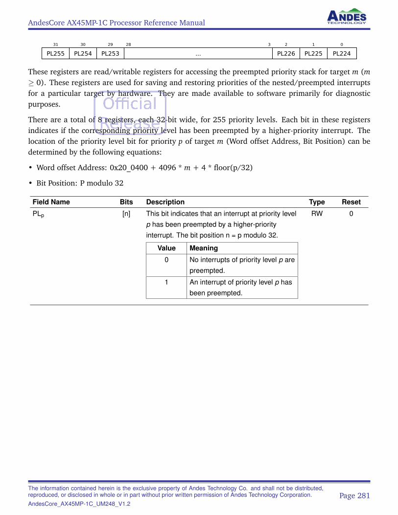
AndesCore AX45MP-1C Processor Reference Manual
31
PL255
30
PL254
29
PL253
28 3
...
2
PL226
1
PL225
0
PL224
These registers are read/writable registers for accessing the preempted priority stack for target m (m≥ 0). These registers are used for saving and restoring priorities of the nested/preempted interruptsfor a particular target by hardware. They are made available to software primarily for diagnosticpurposes.
There are a total of 8 registers, each 32-bit wide, for 255 priority levels. Each bit in these registersindicates if the corresponding priority level has been preempted by a higher-priority interrupt. Thelocation of the priority level bit for priority p of target m (Word offset Address, Bit Position) can bedetermined by the following equations:
• Word offset Address: 0x20_0400 + 4096 * m + 4 * floor(p/32)
• Bit Position: P modulo 32
Field Name Bits Description Type Reset
PLp [n] This bit indicates that an interrupt at priority levelp has been preempted by a higher-priorityinterrupt. The bit position n = p modulo 32.
Value Meaning
0 No interrupts of priority level p arepreempted.
1 An interrupt of priority level p hasbeen preempted.
RW 0
The information contained herein is the exclusive property of Andes Technology Co. and shall not be distributed,reproduced, or disclosed in whole or in part without prior written permission of Andes Technology Corporation.AndesCore_AX45MP-1C_UM248_V1.2
Page 281
AndesCore AX45MP-1C Processor Reference Manual
19 Machine Timer
19.1 Introduction
The RISC-V architecture defines a machine timer that provides a real-time counter and generatestimer interrupts. The Linux kernel expects microsecond resolutions for mtime, so it imposes anadditional requirement that the frequency of the timer clock has to be greater than 1MHz. For non-Linux applications, the timer clock could share the same clock source as the real-time clock timer.
The RISC-V privileged specification expects that software discovers the frequency of the timer clockthrough a platform specific mechanism. For Linux kernels, this is achieved through the Device Treespecification.
The machine timer primarily consists of these memory-mapped registers: mtime and mtimecmpn (n:0 – (NHART-1)). The mtime register is a 64-bit real-time counter clocked by the machine timer clock.
The mtimecmpn register stores a 64-bit value for comparing with mtime. When the value in mtime
is greater than or equal to the value in mtimecmpn, the mstatus.MTIP timer interrupt pending bitwill be set. Once set, the MTIP bit is not cleared until mtimecmp is written.
19.2 Machine Timer Registers
The machine timer registers are accessed through the bus interface, and their memory map is shownin Table 73.
Please note that the machine timer supports only 32-bit or 64-bit transfers. Behaviors of 8-bit and 16-bit transfers are UNDEFINED, and these transfers might be ignored as well as result in error responsesor unexpected register updates.
Table 73: Memory Mapped Machine Timer Registers
Address Offset Description
0x0 – 0x3 mtime[31:0]
0x4 – 0x7 mtime[63:32]
0x8 – 0xB mtimecmp0[31:0]
0xC – 0xF mtimecmp0[63:32]
0x10 – 0x13 mtimecmp1[31:0]
0x14 – 0x17 mtimecmp1[63:32]
0x18 – 0x1B mtimecmp2[31:0]
0x1C – 0x1F mtimecmp2[63:32]
Continued on next page. . .
The information contained herein is the exclusive property of Andes Technology Co. and shall not be distributed,reproduced, or disclosed in whole or in part without prior written permission of Andes Technology Corporation.AndesCore_AX45MP-1C_UM248_V1.2
Page 282
AndesCore AX45MP-1C Processor Reference Manual
Table 73: (continued)
Address Offset Description
0x8+n*8 – 0xB+n*8 mtimecmpn[31:0]
0xC+n*8 – 0xF+n*8 mtimecmpn[63:32]
19.2.1 Machine Timer Initialization
The mtime counter is a 64-bit value and it increments non-stop on every machine timer clock exceptthe first few cycles after its control register updates. When the data bus of machine timer is 64-bit, itis recommended to program the mtime counter through a single double-word store to guarantee thevalue is updated atomically. Otherwise, the following programming sequence should be followed toinitialize the counter through two separate 32-bit updates to mtime[31:0] and mtime[63:32].
• If bit[31:29] of the intended value is 7:
1. Write zero to mtime[31:0].
2. Write high part of the intended value to mtime[63:32].
3. Write low part of the intended value to mtime[31:0].
• Otherwise:
1. Write low part of the intended value to mtime[31:0].
2. Write high part of the intended value to mtime[63:32].
The information contained herein is the exclusive property of Andes Technology Co. and shall not be distributed,reproduced, or disclosed in whole or in part without prior written permission of Andes Technology Corporation.AndesCore_AX45MP-1C_UM248_V1.2
Page 283
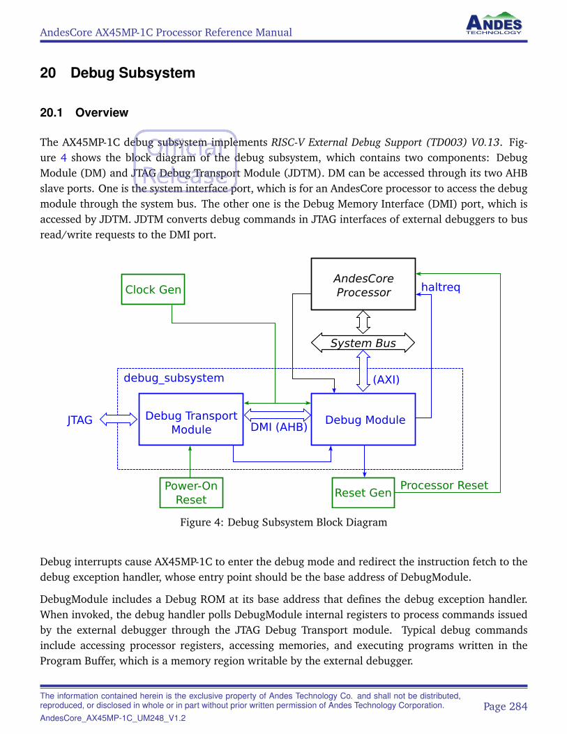
AndesCore AX45MP-1C Processor Reference Manual
20 Debug Subsystem
20.1 Overview
The AX45MP-1C debug subsystem implements RISC-V External Debug Support (TD003) V0.13. Fig-ure 4 shows the block diagram of the debug subsystem, which contains two components: DebugModule (DM) and JTAG Debug Transport Module (JDTM). DM can be accessed through its two AHBslave ports. One is the system interface port, which is for an AndesCore processor to access the debugmodule through the system bus. The other one is the Debug Memory Interface (DMI) port, which isaccessed by JDTM. JDTM converts debug commands in JTAG interfaces of external debuggers to busread/write requests to the DMI port.
AndesCoreProcessor
Processor Reset
Debug ModuleDebug Transport Module
System Bus
debug_subsystem
JTAGDMI (AHB)
(AXI)
Clock Gen
Reset GenPower-On
Reset
haltreq
Figure 4: Debug Subsystem Block Diagram
Debug interrupts cause AX45MP-1C to enter the debug mode and redirect the instruction fetch to thedebug exception handler, whose entry point should be the base address of DebugModule.
DebugModule includes a Debug ROM at its base address that defines the debug exception handler.When invoked, the debug handler polls DebugModule internal registers to process commands issuedby the external debugger through the JTAG Debug Transport module. Typical debug commandsinclude accessing processor registers, accessing memories, and executing programs written in theProgram Buffer, which is a memory region writable by the external debugger.
The information contained herein is the exclusive property of Andes Technology Co. and shall not be distributed,reproduced, or disclosed in whole or in part without prior written permission of Andes Technology Corporation.AndesCore_AX45MP-1C_UM248_V1.2
Page 284
AndesCore AX45MP-1C Processor Reference Manual
20.2 Optional Debug Subsystem
The debug subsystem can be removed by simply disabling the core debug feature in the configurationtool.
The information contained herein is the exclusive property of Andes Technology Co. and shall not be distributed,reproduced, or disclosed in whole or in part without prior written permission of Andes Technology Corporation.AndesCore_AX45MP-1C_UM248_V1.2
Page 285
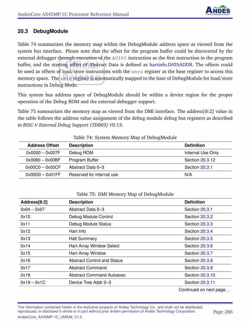
AndesCore AX45MP-1C Processor Reference Manual
20.3 DebugModule
Table 74 summarizes the memory map within the DebugModule address space as viewed from thesystem bus interface. Please note that the offset for the program buffer could be discovered by theexternal debugger through execution of the AUIPC instruction as the first instruction in the programbuffer, and the starting offset of Abstract Data is defined as hartinfo.DATAADDR. The offsets couldbe used as offsets of load/store instructions with the zero register as the base register to access thismemory space. The zero register is automatically mapped to the base of DebugModule for load/storeinstructions in Debug Mode.
This system bus address space of DebugModule should be within a device region for the properoperation of the Debug ROM and the external debugger support.
Table 75 summarizes the memory map as viewed from the DMI interface. The address[8:2] value inthe table follows the address value assignment of the debug module debug bus registers as describedin RISC-V External Debug Support (TD003) V0.13.
Table 74: System Memory Map of DebugModule
Address Offset Description Definition
0x0000 – 0x007F Debug ROM Internal Use Only
0x0080 – 0x00BF Program Buffer Section 20.3.12
0x00C0 – 0x00CF Abstract Data 0–3 Section 20.3.1
0x00D0 – 0x01FF Reserved for internal use N/A
Table 75: DMI Memory Map of DebugModule
Address[8:2] Description Definition
0x04 – 0x07 Abstract Data 0–3 Section 20.3.1
0x10 Debug Module Control Section 20.3.2
0x11 Debug Module Status Section 20.3.3
0x12 Hart Info Section 20.3.4
0x13 Halt Summary Section 20.3.5
0x14 Hart Array Window Select Section 20.3.6
0x15 Hart Array Window Section 20.3.7
0x16 Abstract Control and Status Section 20.3.8
0x17 Abstract Command Section 20.3.9
0x18 Abstract Command Autoexec Section 20.3.10
0x19 – 0x1C Device Tree Addr 0–3 Section 20.3.11
Continued on next page. . .
The information contained herein is the exclusive property of Andes Technology Co. and shall not be distributed,reproduced, or disclosed in whole or in part without prior written permission of Andes Technology Corporation.AndesCore_AX45MP-1C_UM248_V1.2
Page 286
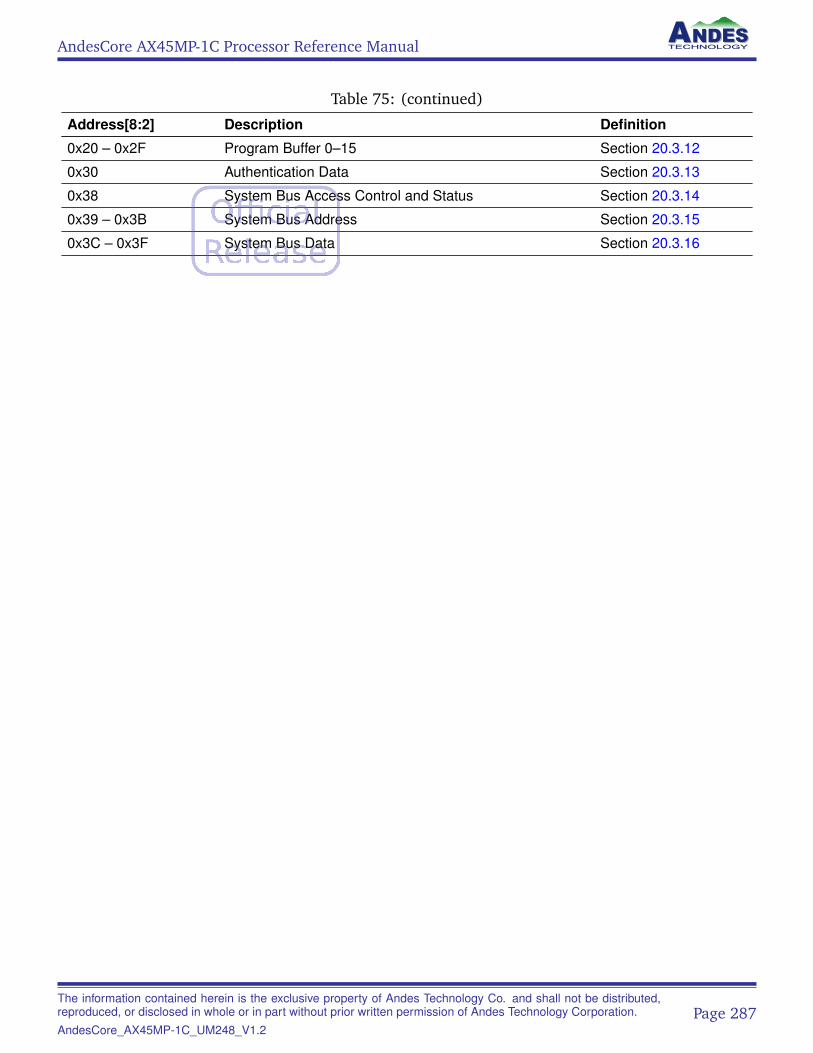
AndesCore AX45MP-1C Processor Reference Manual
Table 75: (continued)
Address[8:2] Description Definition
0x20 – 0x2F Program Buffer 0–15 Section 20.3.12
0x30 Authentication Data Section 20.3.13
0x38 System Bus Access Control and Status Section 20.3.14
0x39 – 0x3B System Bus Address Section 20.3.15
0x3C – 0x3F System Bus Data Section 20.3.16
The information contained herein is the exclusive property of Andes Technology Co. and shall not be distributed,reproduced, or disclosed in whole or in part without prior written permission of Andes Technology Corporation.AndesCore_AX45MP-1C_UM248_V1.2
Page 287
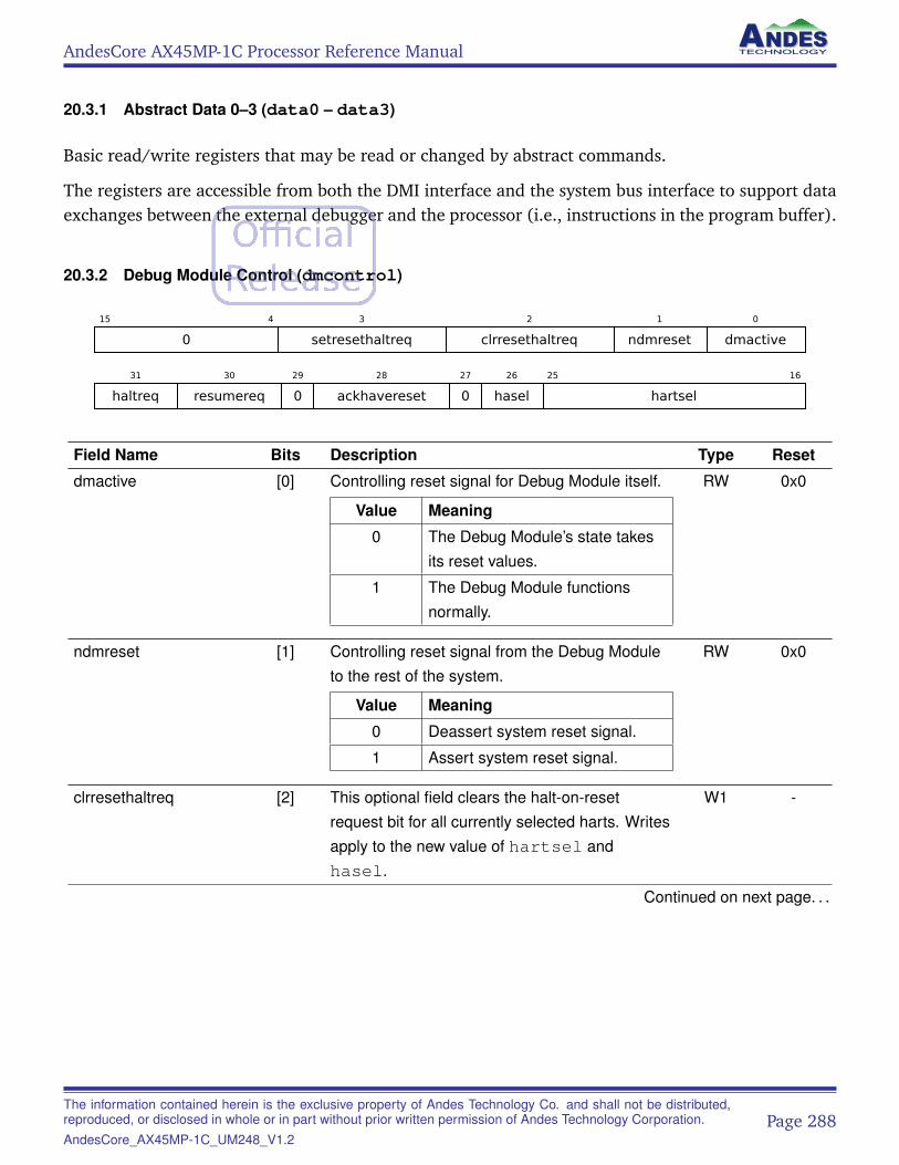
AndesCore AX45MP-1C Processor Reference Manual
20.3.1 Abstract Data 0–3 (data0 – data3)
Basic read/write registers that may be read or changed by abstract commands.
The registers are accessible from both the DMI interface and the system bus interface to support dataexchanges between the external debugger and the processor (i.e., instructions in the program buffer).
20.3.2 Debug Module Control (dmcontrol)
15 4
0
3
setresethaltreq
2
clrresethaltreq
1
ndmreset
0
dmactive
31
haltreq
30
resumereq
29
0
28
ackhavereset
27
0
26
hasel
25 16
hartsel
Field Name Bits Description Type Reset
dmactive [0] Controlling reset signal for Debug Module itself.
Value Meaning
0 The Debug Module’s state takesits reset values.
1 The Debug Module functionsnormally.
RW 0x0
ndmreset [1] Controlling reset signal from the Debug Moduleto the rest of the system.
Value Meaning
0 Deassert system reset signal.
1 Assert system reset signal.
RW 0x0
clrresethaltreq [2] This optional field clears the halt-on-resetrequest bit for all currently selected harts. Writesapply to the new value of hartsel andhasel.
W1 -
Continued on next page. . .
The information contained herein is the exclusive property of Andes Technology Co. and shall not be distributed,reproduced, or disclosed in whole or in part without prior written permission of Andes Technology Corporation.AndesCore_AX45MP-1C_UM248_V1.2
Page 288
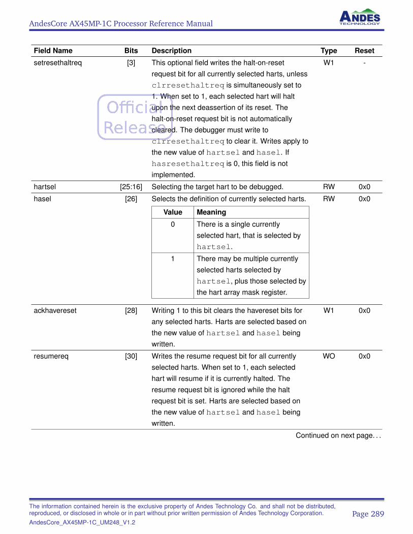
AndesCore AX45MP-1C Processor Reference Manual
Field Name Bits Description Type Reset
setresethaltreq [3] This optional field writes the halt-on-resetrequest bit for all currently selected harts, unlessclrresethaltreq is simultaneously set to1. When set to 1, each selected hart will haltupon the next deassertion of its reset. Thehalt-on-reset request bit is not automaticallycleared. The debugger must write toclrresethaltreq to clear it. Writes apply tothe new value of hartsel and hasel. Ifhasresethaltreq is 0, this field is notimplemented.
W1 -
hartsel [25:16] Selecting the target hart to be debugged. RW 0x0
hasel [26] Selects the definition of currently selected harts.
Value Meaning
0 There is a single currentlyselected hart, that is selected byhartsel.
1 There may be multiple currentlyselected harts selected byhartsel, plus those selected bythe hart array mask register.
RW 0x0
ackhavereset [28] Writing 1 to this bit clears the havereset bits forany selected harts. Harts are selected based onthe new value of hartsel and hasel beingwritten.
W1 0x0
resumereq [30] Writes the resume request bit for all currentlyselected harts. When set to 1, each selectedhart will resume if it is currently halted. Theresume request bit is ignored while the haltrequest bit is set. Harts are selected based onthe new value of hartsel and hasel beingwritten.
WO 0x0
Continued on next page. . .
The information contained herein is the exclusive property of Andes Technology Co. and shall not be distributed,reproduced, or disclosed in whole or in part without prior written permission of Andes Technology Corporation.AndesCore_AX45MP-1C_UM248_V1.2
Page 289
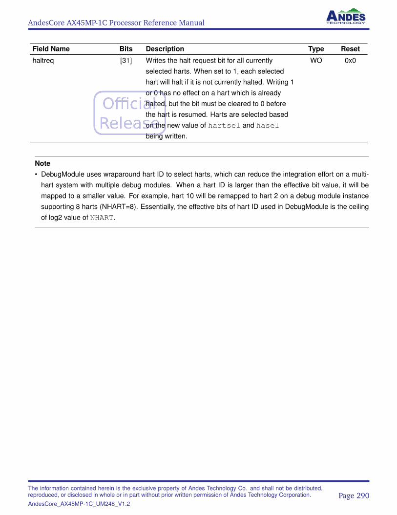
AndesCore AX45MP-1C Processor Reference Manual
Field Name Bits Description Type Reset
haltreq [31] Writes the halt request bit for all currentlyselected harts. When set to 1, each selectedhart will halt if it is not currently halted. Writing 1or 0 has no effect on a hart which is alreadyhalted, but the bit must be cleared to 0 beforethe hart is resumed. Harts are selected basedon the new value of hartsel and haselbeing written.
WO 0x0
Note• DebugModule uses wraparound hart ID to select harts, which can reduce the integration effort on a multi-
hart system with multiple debug modules. When a hart ID is larger than the effective bit value, it will bemapped to a smaller value. For example, hart 10 will be remapped to hart 2 on a debug module instancesupporting 8 harts (NHART=8). Essentially, the effective bits of hart ID used in DebugModule is the ceilingof log2 value of NHART.
The information contained herein is the exclusive property of Andes Technology Co. and shall not be distributed,reproduced, or disclosed in whole or in part without prior written permission of Andes Technology Corporation.AndesCore_AX45MP-1C_UM248_V1.2
Page 290
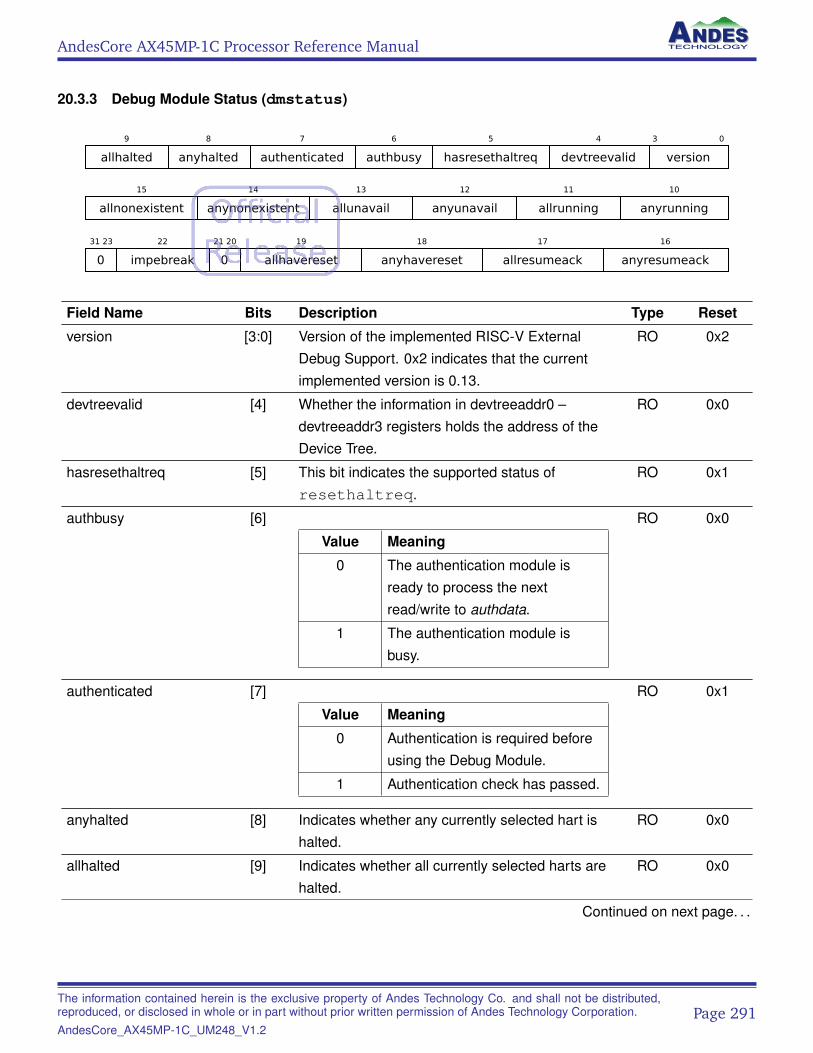
AndesCore AX45MP-1C Processor Reference Manual
20.3.3 Debug Module Status (dmstatus)
9
allhalted
8
anyhalted
7
authenticated
6
authbusy
5
hasresethaltreq
4
devtreevalid
3 0
version
15
allnonexistent
14
anynonexistent
13
allunavail
12
anyunavail
11
allrunning
10
anyrunning
31 23
0
22
impebreak
21 20
0
19
allhavereset
18
anyhavereset
17
allresumeack
16
anyresumeack
Field Name Bits Description Type Reset
version [3:0] Version of the implemented RISC-V ExternalDebug Support. 0x2 indicates that the currentimplemented version is 0.13.
RO 0x2
devtreevalid [4] Whether the information in devtreeaddr0 –devtreeaddr3 registers holds the address of theDevice Tree.
RO 0x0
hasresethaltreq [5] This bit indicates the supported status ofresethaltreq.
RO 0x1
authbusy [6]
Value Meaning
0 The authentication module isready to process the nextread/write to authdata.
1 The authentication module isbusy.
RO 0x0
authenticated [7]
Value Meaning
0 Authentication is required beforeusing the Debug Module.
1 Authentication check has passed.
RO 0x1
anyhalted [8] Indicates whether any currently selected hart ishalted.
RO 0x0
allhalted [9] Indicates whether all currently selected harts arehalted.
RO 0x0
Continued on next page. . .
The information contained herein is the exclusive property of Andes Technology Co. and shall not be distributed,reproduced, or disclosed in whole or in part without prior written permission of Andes Technology Corporation.AndesCore_AX45MP-1C_UM248_V1.2
Page 291
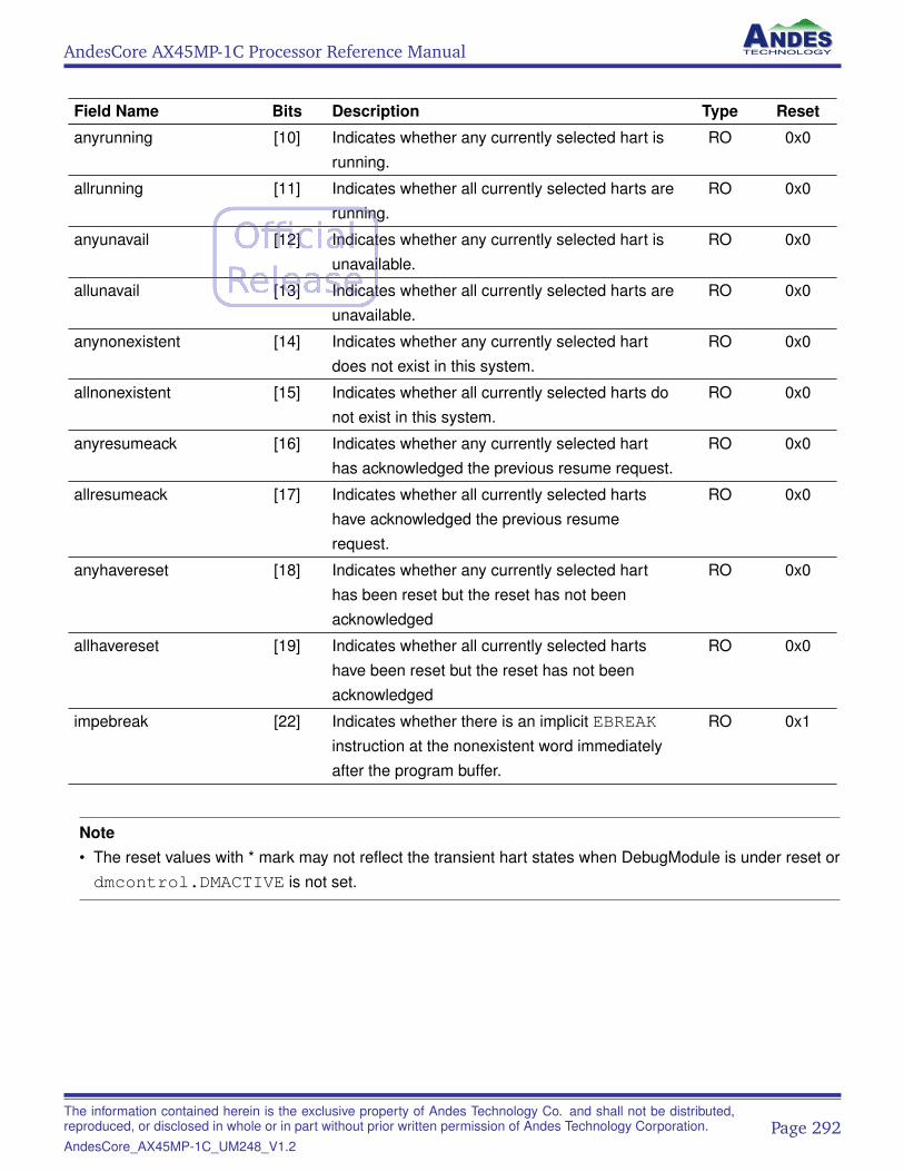
AndesCore AX45MP-1C Processor Reference Manual
Field Name Bits Description Type Reset
anyrunning [10] Indicates whether any currently selected hart isrunning.
RO 0x0
allrunning [11] Indicates whether all currently selected harts arerunning.
RO 0x0
anyunavail [12] Indicates whether any currently selected hart isunavailable.
RO 0x0
allunavail [13] Indicates whether all currently selected harts areunavailable.
RO 0x0
anynonexistent [14] Indicates whether any currently selected hartdoes not exist in this system.
RO 0x0
allnonexistent [15] Indicates whether all currently selected harts donot exist in this system.
RO 0x0
anyresumeack [16] Indicates whether any currently selected harthas acknowledged the previous resume request.
RO 0x0
allresumeack [17] Indicates whether all currently selected hartshave acknowledged the previous resumerequest.
RO 0x0
anyhavereset [18] Indicates whether any currently selected harthas been reset but the reset has not beenacknowledged
RO 0x0
allhavereset [19] Indicates whether all currently selected hartshave been reset but the reset has not beenacknowledged
RO 0x0
impebreak [22] Indicates whether there is an implicit EBREAKinstruction at the nonexistent word immediatelyafter the program buffer.
RO 0x1
Note• The reset values with * mark may not reflect the transient hart states when DebugModule is under reset ordmcontrol.DMACTIVE is not set.
The information contained herein is the exclusive property of Andes Technology Co. and shall not be distributed,reproduced, or disclosed in whole or in part without prior written permission of Andes Technology Corporation.AndesCore_AX45MP-1C_UM248_V1.2
Page 292
AndesCore AX45MP-1C Processor Reference Manual
20.3.4 Hart Info (hartinfo)
31 24
0
23 20
nscratch
19 17
0
16
dataaccess
15 12
datasize
11 0
dataaddr
Field Name Bits Description Type Reset
dataaddr [11:0] Signed offset for accessing the shadowed dataregisters by the processor, to be used as offsetsfor load/store instructions with the zero registeras the base register in Debug Mode.
RO 0xC0
datasize [15:12] Number of 32-bit words in the memory mapdedicated to shadowing the data registers.
RO 0x4
dataaccess [16] The method for accessing the shadowed dataregisters. The value of this field is 0x1 forAX45MP-1C, indicating that the data registersare shadowed in the memory map of theselected hart under Debug Mode.
Value Meaning
0 The data registers are shadowedin the hart by CSR registers.
1 The data registers are shadowedin the hart’s memory map. Eachregister takes up 4 bytes in thememory map.
RO 0x1
nscratch [23:20] Number of dscratch registers available for thedebugger to use during program bufferexecution, starting from dscratch0.
RO 0x2
The information contained herein is the exclusive property of Andes Technology Co. and shall not be distributed,reproduced, or disclosed in whole or in part without prior written permission of Andes Technology Corporation.AndesCore_AX45MP-1C_UM248_V1.2
Page 293
AndesCore AX45MP-1C Processor Reference Manual
20.3.5 Halt Summary (haltsum)
31 1
0
0
halt31_0
Bit 0 contains the logical OR of 32 halt bits for hart 0 – hart 31.
20.3.6 Hart Array Window Select (hawindowsel)
31 15
0
14 0
hawindowsel
Field Name Bits Description Type Reset
hawindowsel [14:0] This register selects which of the 32-bit portionof the hart array mask register is accessible inhawindow.
RW 0x0
20.3.7 Hart Array Window (hawindow)
31 0
hawindow
Field Name Bits Description Type Reset
hawindow [31:0] This register provides R/W accesses to a 32-bitportion of the hart array mask register. Theposition of the window is determined byhawindowsel. That is, bit 0 refers to hart(hawindowsel * 32), while bit 31 refers to hart(hawindowsel * 32 + 31).
RW 0x0
The information contained herein is the exclusive property of Andes Technology Co. and shall not be distributed,reproduced, or disclosed in whole or in part without prior written permission of Andes Technology Corporation.AndesCore_AX45MP-1C_UM248_V1.2
Page 294
AndesCore AX45MP-1C Processor Reference Manual
20.3.8 Abstract Control and Status (abstractcs)
31 29
0
28 24
progbufsize
23 13
0
12
busy
11
0
10 8
cmderr
7 5
0
4 0
datacount
Field Name Bits Description Type Reset
datacount [4:0] Number of data registers that are implemented. RO 0x4
cmderr [10:8] Error code indicating that an abstract commandfails. The bits in this field remain set until theyare cleared by writing 1 to them. No abstractcommand is started until the value is reset to 0.
Value Meaning
0 None: no error
1 Busy: an abstract command wasexecuting while command,abstractcs, or abstractauto waswritten, or when one of the dataor progbuf registers was read orwritten.
2 Not supported: the requestedcommand is not supported.
3 Exception: an exception occurredwhile executing the command.
4 Halt/resume: an abstractcommand cannot executebecause the hart wasn’t in theexpected state (running/halted).
R/W1C 0x0
busy [12] Flag indicating an abstract command is currentlybeing executed.
RO 0x0
progbufsize [28:24] Size of the program buffer, in 32-bit words. RO 0x8
20.3.9 Abstract Command (command)
31 24
cmdtype
23 0
control
The information contained herein is the exclusive property of Andes Technology Co. and shall not be distributed,reproduced, or disclosed in whole or in part without prior written permission of Andes Technology Corporation.AndesCore_AX45MP-1C_UM248_V1.2
Page 295
AndesCore AX45MP-1C Processor Reference Manual
Field Name Bits Description Type Reset
control [23:0] The field is interpreted in a command-specificmanner.
WO 0x0
cmdtype [31:24] Controlling the overall functionality of thisabstract command.
WO 0x0
If a command takes arguments or returns values, they must be written to or placed in the dataregisters. Which data registers are used for the arguments is described in Table 76.
Table 76: Use of Data Registers in PLDM
Argument Width arg0/Return Value arg1 arg2
32 data0 data1 data2
64 data0, data1 data2, data3 data4, data5
20.3.9.1 Access Register
31 24
cmdtype (0)
23
0
22 20
size
19
0
18
postexec
17
transfer
16
write
15 0
regno
This command gives the debugger access to CPU registers and allows CPU to execute the programbuffer.
Field Name Bits Description Type Reset
regno [15:0] Number of the specified register to be accessed. WO 0x0
write [16] The direction of data transfer.
Value Meaning
0 Copy data from the specifiedregister into arg0 portion of theAbstract Data registers.
1 Copy data from arg0 portion ofAbstract Data registers into thespecified register.
WO 0x0
Continued on next page. . .
The information contained herein is the exclusive property of Andes Technology Co. and shall not be distributed,reproduced, or disclosed in whole or in part without prior written permission of Andes Technology Corporation.AndesCore_AX45MP-1C_UM248_V1.2
Page 296
AndesCore AX45MP-1C Processor Reference Manual
Field Name Bits Description Type Reset
transfer [17] Indicates whether to perform data transfer.
Value Meaning
0 Don’t do the operation specifiedby write.
1 Do the operation specified bywrite.
WO 0x0
postexec [18] Indicates whether to execute the program in theprogram buffer.If this field is set, execute the program in theProgram Buffer exactly once after performing thetransfer, if any.
WO 0x0
size [22:20]
Value Meaning
2 Access the lowest 32 bits of theregister
3 Access the lowest 64 bits of theregister.
WO 0x0
20.3.9.2 Quick Access
31 24
cmdtype (1)
23 0
0
Perform the following sequence of operations:
• If the hart is halted already, the command sets cmderr to halt/resume and does not continue.
• Halt the hart. If the hart halts for some other reason (e.g., breakpoint), the command sets cmderrto halt/resume and does not continue.
• Execute the program buffer. If an exception occurs, cmderr is set to exception and the programbuffer execution ends, but the quick access command continues.
• Resume the hart.
The information contained herein is the exclusive property of Andes Technology Co. and shall not be distributed,reproduced, or disclosed in whole or in part without prior written permission of Andes Technology Corporation.AndesCore_AX45MP-1C_UM248_V1.2
Page 297
AndesCore AX45MP-1C Processor Reference Manual
20.3.9.3 Access Memory
31 24
cmdtype (2)
23
aamvirtual
22 20
aamsize
19
aampostincrement
18 17
0
16
write
15 0
0
This command lets the debugger perform memory accesses with the memory view of the selectedhart.
Field Name Bits Description Type Reset
write [16] The direction of data transfer.
Value Meaning
0 Copy data from the memorylocation into arg0 portion of theAbstract Data registers.
1 Copy data from arg0 portion ofAbstract Data registers into thememory location.
WO 0x0
aampostincrement [19] Increment arg1 by the number of bytes encodedin aamsize after a memory access completes.
WO 0x0
aamsize [22:20] Size of memory accesses.
Value Meaning
0 Access the lowest 8 bits of thememory location.
1 Access the lowest 16 bits of thememory location.
2 Access the lowest 32 bits of thememory location.
3 Access the lowest 64 bits of thememory location.
WO 0x0
aamvirtual [23] Virtual or physical address accesses
Value Meaning
0 Addresses are physical
1 No action
WO 0x0
The information contained herein is the exclusive property of Andes Technology Co. and shall not be distributed,reproduced, or disclosed in whole or in part without prior written permission of Andes Technology Corporation.AndesCore_AX45MP-1C_UM248_V1.2
Page 298
AndesCore AX45MP-1C Processor Reference Manual
20.3.10 Abstract Command Autoexec (abstractauto)
31 24
0
23 16
autoexecprogbuf
15 12
0
11 4
0
3 0
autoexecdata
Field Name Bits Description Type Reset
autoexecdata [3:0] When a bit in this field is 1, read or writeaccesses to the corresponding data word causethe command in command to be executed again.
RW 0x0
autoexecprogbuf [23:16] When a bit in this field is 1, read or writeaccesses to the corresponding progbuf wordcause the command in command to be executedagain.
RW 0x0
20.3.11 Device Tree Addr 0–3 (devtreeaddr0 – devtreeaddr3)
The devicetreeaddr registers are hardwired to zeros in DebugModule.
20.3.12 Program Buffer 0–15 (progbuf0 – progbuf15)
31 0
data
The progbuf registers provide read/write accesses to the program buffer. DebugModule supports pro-gram buffer 0–7 only. Program buffer 8–15 are hardwired to 0x00100073 (the EBREAK instruction).
These registers are read/write accessible from both the DMI interface and the system bus, in additionto being a valid region for instruction fetches. They hold small programs written by the externaldebugger and these small programs will be fetched and executed by the processor upon execution ofthe abstract commands which require execution of the program buffer.
Programs in progbuf must end with EBREAK or C.EBREAK instructions if the program size is less than8 words (32 bytes).
20.3.13 Authentication Data (authdata)
The authdata register is hardwired to zeros in DebugModule.
The information contained herein is the exclusive property of Andes Technology Co. and shall not be distributed,reproduced, or disclosed in whole or in part without prior written permission of Andes Technology Corporation.AndesCore_AX45MP-1C_UM248_V1.2
Page 299
AndesCore AX45MP-1C Processor Reference Manual
20.3.14 System Bus Access Control and Status (sbcs)
15
sbreadondata
14 12
sberror
11 5
sbasize
4
sbaccess128
3
sbaccess64
2
sbaccess32
1
sbaccess16
0
sbaccess8
31 29
sbversion
28 23
0
22
sbbusyerror
21
sbbusy
20
sbreadonaddr
19 17
sbaccess
16
sbautoincrement
The sbcs register holds the control bits and status flags of System Bus Accesses. It is only valid whenthe SYSTEM_BUS_ACCESS_SUPPORT parameter of DebugModule is set. It is otherwise hardwired tozero.
Field Name Bits Description Type Reset
sbaccess8 [0] This bit indicates the supported status of8-bit system bus data accesses.
RO 0x1
sbaccess16 [1] This bit indicates the supported status of16-bit system bus data accesses.
RO 0x1
sbaccess32 [2] This bit indicates the supported status of32-bit system bus data accesses.
RO 0x1
sbaccess64 [3] This bit indicates the supported status of64-bit system bus data accesses. This bit is1 if SYS_DATA_WIDTH == 64.
RO ConfigurationDependent
sbaccess128 [4] This bit indicates the supported status of128-bit system bus data accesses.
RO 0x0
sbasize [11:5] Address width of System bus addresses inbits. This field is 0 if there is no bus accesssupport. Otherwise, it is the value of theSYS_ADDR_WIDTH parameter ofDebugModule.
RO ConfigurationDependent
Continued on next page. . .
The information contained herein is the exclusive property of Andes Technology Co. and shall not be distributed,reproduced, or disclosed in whole or in part without prior written permission of Andes Technology Corporation.AndesCore_AX45MP-1C_UM248_V1.2
Page 300
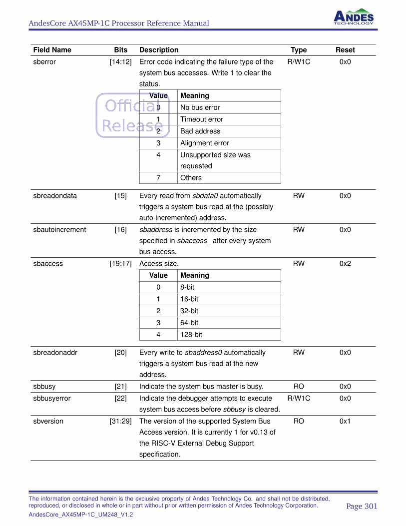
AndesCore AX45MP-1C Processor Reference Manual
Field Name Bits Description Type Reset
sberror [14:12] Error code indicating the failure type of thesystem bus accesses. Write 1 to clear thestatus.
Value Meaning
0 No bus error
1 Timeout error
2 Bad address
3 Alignment error
4 Unsupported size wasrequested
7 Others
R/W1C 0x0
sbreadondata [15] Every read from sbdata0 automaticallytriggers a system bus read at the (possiblyauto-incremented) address.
RW 0x0
sbautoincrement [16] sbaddress is incremented by the sizespecified in sbaccess_ after every systembus access.
RW 0x0
sbaccess [19:17] Access size.
Value Meaning
0 8-bit
1 16-bit
2 32-bit
3 64-bit
4 128-bit
RW 0x2
sbreadonaddr [20] Every write to sbaddress0 automaticallytriggers a system bus read at the newaddress.
RW 0x0
sbbusy [21] Indicate the system bus master is busy. RO 0x0
sbbusyerror [22] Indicate the debugger attempts to executesystem bus access before sbbusy is cleared.
R/W1C 0x0
sbversion [31:29] The version of the supported System BusAccess version. It is currently 1 for v0.13 ofthe RISC-V External Debug Supportspecification.
RO 0x1
The information contained herein is the exclusive property of Andes Technology Co. and shall not be distributed,reproduced, or disclosed in whole or in part without prior written permission of Andes Technology Corporation.AndesCore_AX45MP-1C_UM248_V1.2
Page 301
AndesCore AX45MP-1C Processor Reference Manual
NoteThe states of sbaccess8 – sbaccess128 are set based on the SYS_ADDR_WIDTH parameter in DebugMod-ule.
20.3.15 System Bus Address (sbaddress0 – sbaddress2)
The sbaddress registers are only valid when the SYSTEM_BUS_ACCESS_SUPPORT parameter of De-bugModule is set. They are otherwise hardwired to zeros.
Table 77: System Bus Address Register
Address Register Description
sbaddress0 bit[31:0] of the address in sbaddress
sbaddress1 bit[63:32] of the address in sbaddress
sbaddress2 bit[95:64] of the address in sbaddress
sbaddress3 bit[127:96] of the address in sbaddress
20.3.16 System Bus Data (sbdata0 – sbdata3)
The sbdata register is supported as below when SYSTEM_BUS_ACCESS_SUPPORT parameter of De-bugModule is set. Otherwise it is hardwired to zeros.
Table 78: System Bus Data Register
Address Register Description
sbdata0 bit [31:0] of the address in sbdata
sbdata1 bit [63:32] of the address in sbdata
sbdata2 bit [95:64] of the address in sbdata
sbdata3 bit [127:96] of the address in sbdata
20.4 JTAG Debug Transport Module
JDTM is an implementation of the JTAG debug transport module (DTM), as defined by the spec:RISC-V External Debug Support (TD003) V0.13. It implements the IEEE 1149.1 style test access portcontroller (TAP). The supported instructions are summarized in Table 79.
The information contained herein is the exclusive property of Andes Technology Co. and shall not be distributed,reproduced, or disclosed in whole or in part without prior written permission of Andes Technology Corporation.AndesCore_AX45MP-1C_UM248_V1.2
Page 302
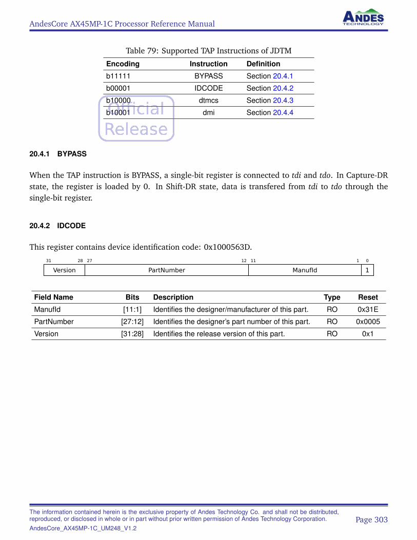
AndesCore AX45MP-1C Processor Reference Manual
Table 79: Supported TAP Instructions of JDTM
Encoding Instruction Definition
b11111 BYPASS Section 20.4.1
b00001 IDCODE Section 20.4.2
b10000 dtmcs Section 20.4.3
b10001 dmi Section 20.4.4
20.4.1 BYPASS
When the TAP instruction is BYPASS, a single-bit register is connected to tdi and tdo. In Capture-DRstate, the register is loaded by 0. In Shift-DR state, data is transfered from tdi to tdo through thesingle-bit register.
20.4.2 IDCODE
This register contains device identification code: 0x1000563D.
31 28
Version
27 12
PartNumber
11 1
ManufId
0
1
Field Name Bits Description Type Reset
ManufId [11:1] Identifies the designer/manufacturer of this part. RO 0x31E
PartNumber [27:12] Identifies the designer’s part number of this part. RO 0x0005
Version [31:28] Identifies the release version of this part. RO 0x1
The information contained herein is the exclusive property of Andes Technology Co. and shall not be distributed,reproduced, or disclosed in whole or in part without prior written permission of Andes Technology Corporation.AndesCore_AX45MP-1C_UM248_V1.2
Page 303
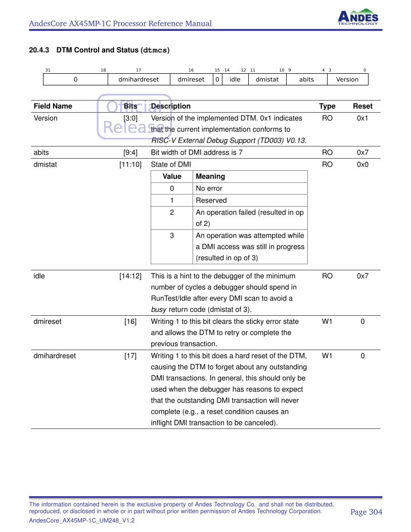
AndesCore AX45MP-1C Processor Reference Manual
20.4.3 DTM Control and Status (dtmcs)
31 18
0
17
dmihardreset
16
dmireset
15
0
14 12
idle
11 10
dmistat
9 4
abits
3 0
Version
Field Name Bits Description Type Reset
Version [3:0] Version of the implemented DTM. 0x1 indicatesthat the current implementation conforms toRISC-V External Debug Support (TD003) V0.13.
RO 0x1
abits [9:4] Bit width of DMI address is 7 RO 0x7
dmistat [11:10] State of DMI
Value Meaning
0 No error
1 Reserved
2 An operation failed (resulted in opof 2)
3 An operation was attempted whilea DMI access was still in progress(resulted in op of 3)
RO 0x0
idle [14:12] This is a hint to the debugger of the minimumnumber of cycles a debugger should spend inRunTest/Idle after every DMI scan to avoid abusy return code (dmistat of 3).
RO 0x7
dmireset [16] Writing 1 to this bit clears the sticky error stateand allows the DTM to retry or complete theprevious transaction.
W1 0
dmihardreset [17] Writing 1 to this bit does a hard reset of the DTM,causing the DTM to forget about any outstandingDMI transactions. In general, this should only beused when the debugger has reasons to expectthat the outstanding DMI transaction will nevercomplete (e.g., a reset condition causes aninflight DMI transaction to be canceled).
W1 0
The information contained herein is the exclusive property of Andes Technology Co. and shall not be distributed,reproduced, or disclosed in whole or in part without prior written permission of Andes Technology Corporation.AndesCore_AX45MP-1C_UM248_V1.2
Page 304
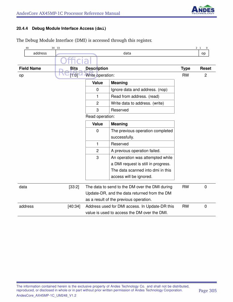
AndesCore AX45MP-1C Processor Reference Manual
20.4.4 Debug Module Interface Access (dmi)
The Debug Module Interface (DMI) is accessed through this register.
40 34
address
33 2
data
1 0
op
Field Name Bits Description Type Reset
op [1:0] Write operation:
Value Meaning
0 Ignore data and address. (nop)
1 Read from address. (read)
2 Write data to address. (write)
3 Reserved
Read operation:
Value Meaning
0 The previous operation completedsuccessfully.
1 Reserved
2 A previous operation failed.
3 An operation was attempted whilea DMI request is still in progress.The data scanned into dmi in thisaccess will be ignored.
RW 2
data [33:2] The data to send to the DM over the DMI duringUpdate-DR, and the data returned from the DMas a result of the previous operation.
RW 0
address [40:34] Address used for DMI access. In Update-DR thisvalue is used to access the DM over the DMI.
RW 0
The information contained herein is the exclusive property of Andes Technology Co. and shall not be distributed,reproduced, or disclosed in whole or in part without prior written permission of Andes Technology Corporation.AndesCore_AX45MP-1C_UM248_V1.2
Page 305