an electro-thermal approach to dielectric breakdown in solids: application to crystalline polymer...
TRANSCRIPT
1038 A. M. N. Lima et al.: Refined Dielectric Breakdown Model for Crystalline Organic Insulators: Electro-thermal Instability
1070-9878/11/$25.00 © 2011 IEEE
Refined Dielectric Breakdown Model for Crystalline Organic Insulators: Electro-thermal Instability
Coupled to Interband Impact Ionization
A. M. N. Lima1, A. G. S. Barreto Neto1,3, E. U. K. Melcher2,4 and H. Neff1,4
1Department of Electrical Engineering - DEE Center for Electrical Engineering and Informatics - CEEI
Universidade Federal de Campina Grande– UFCG Rua Aprígio Veloso, 882, 58429-900,Caixa Postal 10.105, Campina Grande, PB, Brazil
2Department of Systems and Computing – CEEI/UFCG
3DepartmentofElectromechanics, Instituto Federal da Paraíba Rua José Antonio da Silva, 300, Cajazeiras, PB, Brazil
4Center for Strategic Research - CETENE and Laboratory for Integrated Circuits and Systems - LINCS Av. Prof. Luís Freire, 1, Cidade Universitária, 50.740-540 Recife, PE, Brazil
ABSTRACT
A refined, substantially improved dielectric breakdown model is presented and applied to solution grown, single crystalline alkane type polymeric (n-C36H74) insulator, representing the iso-electronic analog to polyethylene. Ultraviolet illumination of attached electrodes allows controlled generation, injection into and transport of free charge carriers through the insulator. At sufficiently high electric fields, carrier transport is mediated by delocalized states in the conduction and valence band, respectively. At low and moderate fields, charge transport is suppressed by carrier trapping effects. Electric field induced inter-band impact ionization and generation of electron-hole pairs has been identified from these experiments as the dominant carrier multiplication and breakdown triggering mechanism. Critical field magnitudes >1.26 MV/cm have been recorded experimentally for injected electrons and >0.8 MV/cm for defect electrons, in reasonable agreement with the theoretical model. Application of the energy conservation principle, in accord with the solid state band model, allows determination of critical fields from the insulators electronic band-gap, effective mass and mobility of minority charge carriers. The related electrical breakdown feature and associated rapid dynamic temperature evolution has been explored on basis of the electro-thermal heat balance equation, following previous concepts applied to phase transitions. The non-linear differential equation has been solved numerically, using appropriate thermo-physical materials parameters, while considering the dielectric breakdown phenomenon as a singularity of the solution. Thermal and current run-away is due to strong positive electro-thermal feedback, in connection with an initial transient resistive behavior. Very small thermo-physical parameters are attributed to and explain filamentary charge transport. The temporal evolution of temperature and current in the conducting section or filament during the breakdown event exhibits a time scale up to the microsecond range. Shock wave emission is apparent, since the spatial temperature propagation exceeds the velocity of sound.
Index Terms — Dielectric breakdown, electro-thermal instability, crystalline organic insulators, impact ionization.
Manuscript received on 11 September 2010, in final form 20 November 2010.
IEEE Transactions on Dielectrics and Electrical Insulation Vol. 18, No. 4; August 2011 1039
1 INTRODUCTION
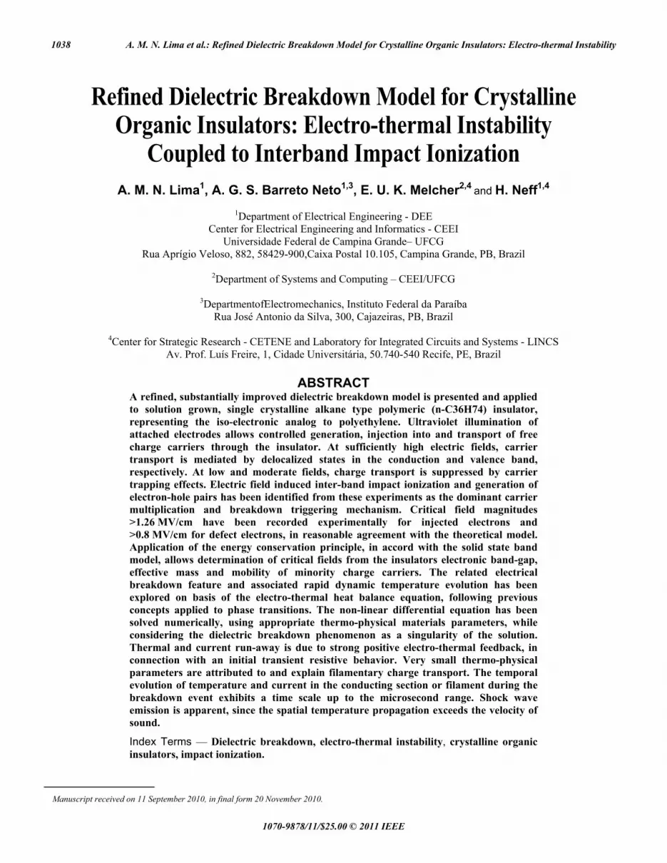
THE dielectric breakdown phenomenon in solid insulators as well as sparking in gas atmosphere is considered as the dominant damage mechanism in high voltage/high power switching, transmission and distribution devices. Due to the complexity and variety of observed breakdown events, a rather large number of theories and breakdown models have been developed over an extended period [1-4]. Recorded breakdown fields span from 1 MV/cm for crystalline, to over 10 MV/cm for fully amorphous material [5-6]. An extensive, critical review and analysis of present theories in solids under transient conditions has been provided in [7].However, the large variety of breakdown conditions in solid insulators makes a single and general theory a particularly difficult undertaking. Figure 1 reveals a representative statistical evolution of publications and related research activities, with data taken from ISI Web of knowledge. Apparently, rather limited scientific and technological progress has been achieved on this topic over a rather long time span of nearly 40 years until 1990, whilst a steep increase in research activities is eminent over the last 20 years. This is related to both, improved public funding and industrial R&D efforts within the electric power generation and distribution sector, in response to the worldwide steady increase of energy consumption, along with higher demand on grid capacity and technology. One of the first major industrial research project son dielectric breakdown and aging in polymeric insulators was successfully launched in the mid 80’s at the ABBR&D-Center in Switzerland, and conducted by. Zeller [8]. Among other aspects, there are four primary features that should emerge from a reliable solid dielectric breakdown model:1. occurrence of temperature/current instability and run-away, 2. criticality, existence of a critical field / voltage; 3. strong spatial limitation, connected to filamentary charge transport and 4. reasoning acoustic shock-wave emission.
In this work, an attempt has been made to combine an initial, electric field induced carrier multiplication process via band impact ionization with an electro-thermal approach. This route follows earlier concepts, applied to solid state phase transitions. Dielectric breakdown ultimately appears as instability, due to presence of a strong positive electro-thermal feedback loop. It leads to current run-away and uncontrolled excessive Joule heating in the conducting section. Increase in electrical conduction occurs at very high temperature, along with light emission and even local plasma formation.
The destructive nature of the breakdown phenomenon thus primarily originates from an explosive increase of temperature. Catastrophic damage of the insulator device originates from all: thermal chemical bond breaking, local electro-mechanical stress by material expansion and vaporization and/or thermally induced chemical (oxidation) reactions in the filamentary conduction channel. Furthermore, the spatially limited, rapid increase of temperature and pressure in the conducting channels also accounts for local acoustic shockwave emissions, when the avalanche propagation velocity exceeds the speed of sound, typically experienced as a sharp bang.
2 THEORETICAL ASPECTS Mathematically, the dielectric breakdown phenomenon is
described as a singularity in the temporal evolution of the total current density
hehe jjj ,that varies with a large number of
physical parameters [9]:
)1(),,(),,(),,,( ,,,, rEErj tnnETTtnq hehehehe
The resistivity is obtained as )/(1 ,,,, hehehehe nq ,and the
associated carrier density )/(1 ,,,, hehehehe qn ,heq ,is the
elementary electron (e) and hole (h) charge, t is time, r isthe spatial coordinate,
hen ,is the carrier density, T is the temperature,
he , is the respective carrier mobility tensor, and E the persistent
electric field vector. All physical parameters are interrelated, and an attempt has been made in this work to simultaneously address the influence of electric field and temperature, whilst simplifying to isotropic conditions.
2.1 IMPACT IONIZATION AND CRITICAL FIELD
In the absence of strong defect scattering and trap controlled transport at high internal electric fields E, close to dielectric breakdown conditions, mobile charges within the insulator’s
Figure 1. Evolution of research and development activity over a time span of sixty years, taken from the number of published articles, associated with key words “dielectric breakdown”, “theory” and “solid insulator”.
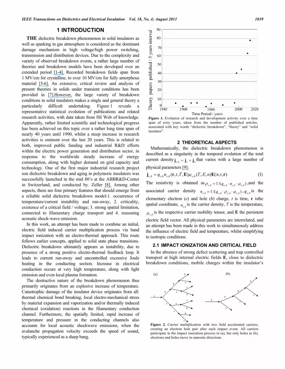
Figure 2. Carrier multiplication with two field accelerated carriers, creating an electron hole pair after each impact event. All carriers participate in the impact ionization process in (a), but only holes in (b), electrons and holes move in opposite directions.
1040 A. M. N. Lima et al.: Refined Dielectric Breakdown Model for Crystalline Organic Insulators: Electro-thermal Instability volume can accelerate to kinetic energies that correspond to its intrinsic band-gap value UG. In crystalline solids, the material´s specific quantity is defined as the energetic distance between the lowest unoccupied state in the conduction and the highest occupied electron state in the valence band. For amorphous polyethylene, and the alkane crystal under consideration, UG has been determined to 8.8 eV in [10]. As the gain in kinetic energy in the electric field approaches this value, strong resonant electron-electron interactions of mobile charges with the electron system in the valence band occurs, accounting for electron-hole pair generation by inelastic impact.
The cascading process is illustrated in Figures 2a and 2b. For each electron-electron or electron-hole impact ionization event, a second free electron in the conduction band, and a further mobile positively charged defect electron (hole) in the valence band are created. The critical field for solid state impact ionization simply requires that the gain of kinetic particle energy under influence of the insulator’s internal electric field E exceeds the energy, needed for creation of a new electron-hole pair. This energy is defined by the optical band gap (UG) of the material:
)2(2
1 2,, Ghehe eUvm
The gain of particle velocity in the electric field in the bulk of a crystalline or polycrystalline insulator is determined by
Ehe,v and me,h being the effective mass tensor. Thus, the
lower electric field bound for carrier multiplication impcritE (via
electron-hole pair generation by interband impact ionization across the optical band-gap)is given by
)3()(
22,, hehe
Gimpcrit m
eUE
The dynamic characteristics can be accessed from the carrier drift behavior at high fields, given by
)4()/( , crithecrit Es
where
crit is the time span required to gain sufficient energy
for creating a new electron-hole pair by impact ionization over a given drift length s. It is usually set at a range of micrometers, yielding to
crit values in the range of
nanoseconds. The fast dynamics rapidly increases the mobile carrier density, along with a decrease of resistance, provided that local electric fields are not limited by trapped charge carriers. This concept thus represents the solid state analog to field induced carrier multiplication by impact ionization in gases that is well described by the classical theory of Townsend [11]. A further important aspect is that typically only electrons have been considered in current breakdown theories although both, electrons and their positively charged counterparts equivalently co-exist within the band-structure concept at solid-solid interfaces, being essential to maintain charge balance. Earlier results, applying (3)
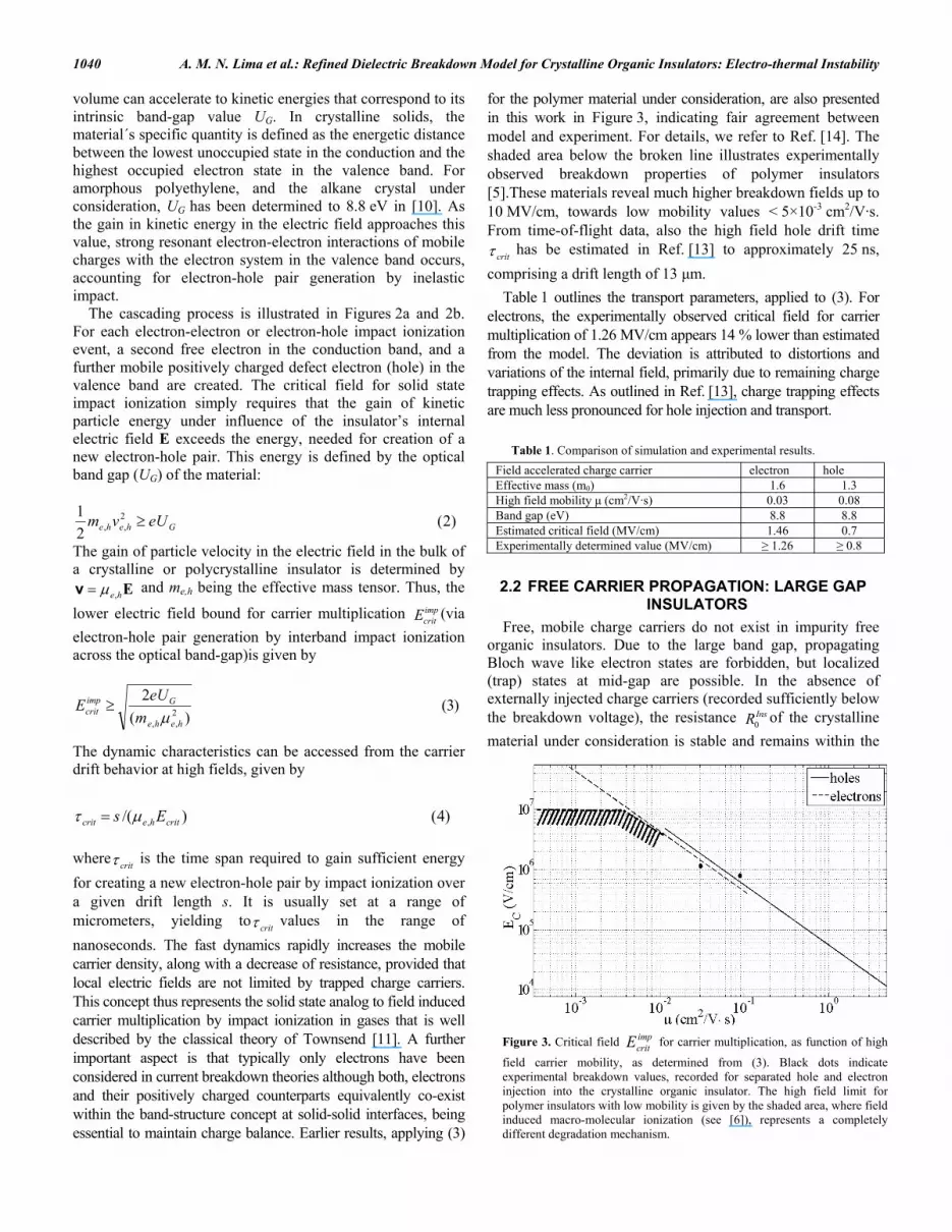
for the polymer material under consideration, are also presented in this work in Figure 3, indicating fair agreement between model and experiment. For details, we refer to Ref. [14]. The shaded area below the broken line illustrates experimentally observed breakdown properties of polymer insulators [5].These materials reveal much higher breakdown fields up to 10 MV/cm, towards low mobility values < 5×10⁻³ cm2/V·s. From time-of-flight data, also the high field hole drift time
crit has be estimated in Ref. [13] to approximately 25 ns,
comprising a drift length of 13 μm.
Table 1 outlines the transport parameters, applied to (3). For electrons, the experimentally observed critical field for carrier multiplication of 1.26 MV/cm appears 14 % lower than estimated from the model. The deviation is attributed to distortions and variations of the internal field, primarily due to remaining charge trapping effects. As outlined in Ref. [13], charge trapping effects are much less pronounced for hole injection and transport.
Table 1. Comparison of simulation and experimental results.
Field accelerated charge carrier electron hole Effective mass (m0) 1.6 1.3 High field mobility μ (cm2/V·s) 0.03 0.08 Band gap (eV) 8.8 8.8 Estimated critical field (MV/cm) 1.46 0.7 Experimentally determined value (MV/cm) ≥ 1.26 ≥ 0.8
2.2 FREE CARRIER PROPAGATION: LARGE GAP INSULATORS
Free, mobile charge carriers do not exist in impurity free organic insulators. Due to the large band gap, propagating Bloch wave like electron states are forbidden, but localized (trap) states at mid-gap are possible. In the absence of externally injected charge carriers (recorded sufficiently below the breakdown voltage), the resistance InsR0
of the crystalline
material under consideration is stable and remains within the
Figure 3. Critical field imp
critE for carrier multiplication, as function of high
field carrier mobility, as determined from (3). Black dots indicate experimental breakdown values, recorded for separated hole and electron injection into the crystalline organic insulator. The high field limit for polymer insulators with low mobility is given by the shaded area, where field induced macro-molecular ionization (see [6]), represents a completely different degradation mechanism.
IEEE Transactions on Dielectrics and Electrical Insulation Vol. 18, No. 4; August 2011 1041 range 1010 to 1013 Ω, crucially depending on material’s quality and preparation conditions.
As mentioned before, photo-excitation at voltage biased electrodes and injection of a photo-current into the bulk insulator represents an appropriate method for generation of mobile, (hot) electrons or defect electrons (holes). These quantum particles typically exhibit kinetic energies within the eV range. For example, irradiation with (UV) photons ≥ 4.4 eV (half band-gap energy) accounts for photo-injection of mobile electrons at a negatively biased cathode (or of holes at anodic potentials), provided that an optically transmitting counter electrode is mounted. They are designed as conducting aqueous electrolyte contacts that prevent parasitic carrier injection, thus driving an externally controlled current through the material. For experimental details of free carrier photo-injection into large gap organic insulators, we refer to [13].
Revealing excess kinetic energies much larger than kT, photo-excited charge carriers overcome the surface barrier and escape from the illuminated electrode surface into the organic insulator. In presence of sufficiently high internal fields, they will propagate through the solid insulator, while maintaining energy levels within its conduction or valence bands, respectively, along with reasonably long life times.
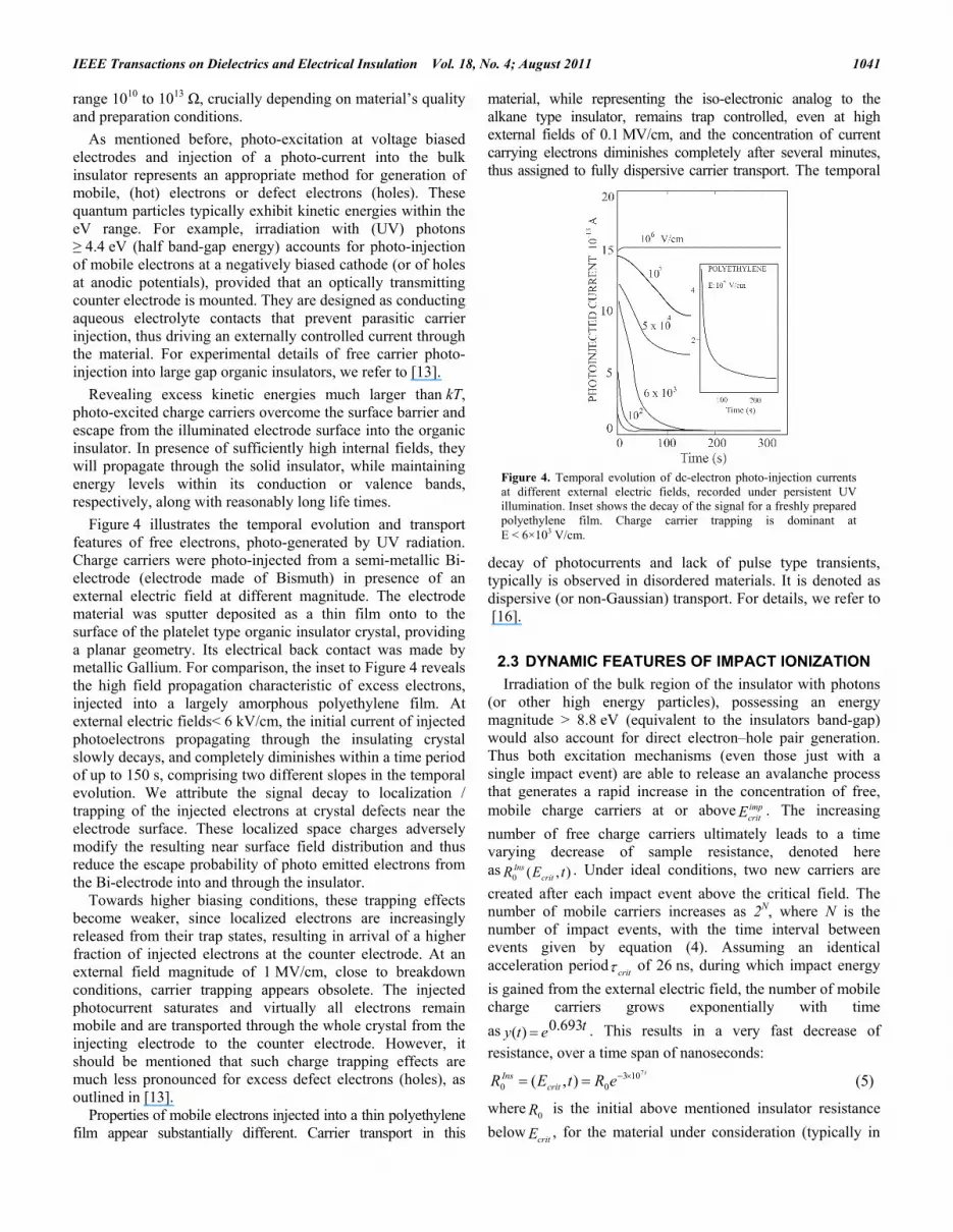
Figure 4 illustrates the temporal evolution and transport features of free electrons, photo-generated by UV radiation. Charge carriers were photo-injected from a semi-metallic Bi-electrode (electrode made of Bismuth) in presence of an external electric field at different magnitude. The electrode material was sputter deposited as a thin film onto to the surface of the platelet type organic insulator crystal, providing a planar geometry. Its electrical back contact was made by metallic Gallium. For comparison, the inset to Figure 4 reveals the high field propagation characteristic of excess electrons, injected into a largely amorphous polyethylene film. At external electric fields< 6 kV/cm, the initial current of injected photoelectrons propagating through the insulating crystal slowly decays, and completely diminishes within a time period of up to 150 s, comprising two different slopes in the temporal evolution. We attribute the signal decay to localization / trapping of the injected electrons at crystal defects near the electrode surface. These localized space charges adversely modify the resulting near surface field distribution and thus reduce the escape probability of photo emitted electrons from the Bi-electrode into and through the insulator.
Towards higher biasing conditions, these trapping effects become weaker, since localized electrons are increasingly released from their trap states, resulting in arrival of a higher fraction of injected electrons at the counter electrode. At an external field magnitude of 1 MV/cm, close to breakdown conditions, carrier trapping appears obsolete. The injected photocurrent saturates and virtually all electrons remain mobile and are transported through the whole crystal from the injecting electrode to the counter electrode. However, it should be mentioned that such charge trapping effects are much less pronounced for excess defect electrons (holes), as outlined in [13].
Properties of mobile electrons injected into a thin polyethylene film appear substantially different. Carrier transport in this
material, while representing the iso-electronic analog to the alkane type insulator, remains trap controlled, even at high external fields of 0.1 MV/cm, and the concentration of current carrying electrons diminishes completely after several minutes, thus assigned to fully dispersive carrier transport. The temporal
decay of photocurrents and lack of pulse type transients, typically is observed in disordered materials. It is denoted as dispersive (or non-Gaussian) transport. For details, we refer to [16].
2.3 DYNAMIC FEATURES OF IMPACT IONIZATION
Irradiation of the bulk region of the insulator with photons (or other high energy particles), possessing an energy magnitude > 8.8 eV (equivalent to the insulators band-gap) would also account for direct electron–hole pair generation. Thus both excitation mechanisms (even those just with a single impact event) are able to release an avalanche process that generates a rapid increase in the concentration of free, mobile charge carriers at or above imp
critE . The increasing
number of free charge carriers ultimately leads to a time varying decrease of sample resistance, denoted here as ),(0 tER crit
Ins . Under ideal conditions, two new carriers are
created after each impact event above the critical field. The number of mobile carriers increases as 2N, where N is the number of impact events, with the time interval between events given by equation (4). Assuming an identical acceleration period
crit of 26 ns, during which impact energy
is gained from the external electric field, the number of mobile charge carriers grows exponentially with time
as tety 693.0)( . This results in a very fast decrease of
resistance, over a time span of nanoseconds:
)5(),(7103
00
t
eRtER critIns
where0R is the initial above mentioned insulator resistance
belowcritE , for the material under consideration (typically in
Figure 4. Temporal evolution of dc-electron photo-injection currents at different external electric fields, recorded under persistent UV illumination. Inset shows the decay of the signal for a freshly prepared polyethylene film. Charge carrier trapping is dominant at E < 6×10³ V/cm.
1042 A. M. N. Lima et al.: Refined Dielectric Breakdown Model for Crystalline Organic Insulators: Electro-thermal Instability excess of 1010 Ω).In practice, a certain fraction of created carriers will be trapped and not contribute to the current, or will not accelerate to high enough energy, or will be captured within the near electrode image potential. For insulators that reveal an optical band gap UG and thermally activated electrical conduction, the temperature coefficient of resistance (TCR) is negative and can be approximated by
20
1)(
ins
B
dT
dR
RT
with )6(
2k
UB G
where k is the Boltzmann constant and UGis the thermal activation energy, considered here as a temperature independent optical band gap of 8.8 eV of the insulator material, with B determined to 5,116.27.
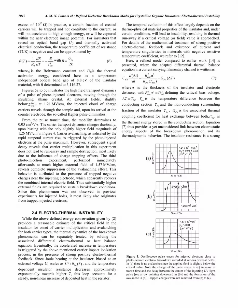
Figures 5a to 5c illustrates the high field transport dynamics of a pulse of photo-injected electrons, moving through the insulating alkane crystal. At external fields, slightly below imp
critE , at 1.21 MV/cm, the injected cloud of charge
carriers travels through the sample and, upon its arrival at the counter electrode, the so-called Kepler pulse diminishes.
From the pulse transit time, the mobility determines to 0.03 cm2/V·s. The carrier transport dynamics changes drastically, upon biasing with the only slightly higher field magnitude of 1.26 MV/cm in Figure 4. Carrier avalanching, as indicated by the rapid temporal current rise, is triggered by the photo-injected electrons at the pulse maximum. However, subsequent signal decay reveals that carrier multiplication in this experiment does not lead to run-away and sample destruction, most likely due to the influence of charge trapping effects. The third photo-injection experiment, performed immediately afterwards at much higher external field of 1.57 MV/cm, reveals complete suppression of the avalanching effect. This behavior is attributed to the presence of trapped negative charges near the injecting electrode, which apparently reduces the combined internal electric field. Thus substantially higher external fields are required to sustain breakdown conditions. Since this phenomenon was not observed in previous experiments for injected holes, it most likely also originates from trapped injected electrons.
2.4 ELECTRO-THERMAL INSTABILITY
While the above defined energy conservation given by (2) provides a reasonable estimate of the critical field in the insulator for onset of carrier multiplication and avalanching for both carrier types, the thermal dynamics of the breakdown phenomenon can be separately treated by solving the associated differential electro-thermal or heat balance equation. Eventually, the accelerated increase in temperature is triggered by the above mentioned carrier impact ionization process, in the presence of strong positive electro-thermal feedback. Since Joule heating at the insulator, biased at an external voltage U, scales as )(/2 TRU Ins
, and the temperature
dependent insulator resistance decreases approximately exponentially towards higher T, this loop accounts for a steady, non-linear increase of deposited heat in the resistor.
The temporal evolution of this effect largely depends on the thermo-physical material properties of the insulator and, under certain conditions, will lead to instability, resulting in thermal run-away if a critical voltage (or field) value is approached. For details of the mathematical treatment of strong positive electro-thermal feedback and existence of current and temperature singularities in materials with negative resistive temperature coefficient, we refer to [12].
Here, a refined model compared to earlier work [14] is presented, where the adapted differential thermal balance equation in a current carrying filamentary channel is written as
)7()()(
)( 22
TGTR
aE
dt
tdC Fil
InsIns
critFil
where a is the thickness of the insulator and electrode distance, with 222
critcrit UaE defining the critical bias voltage.
InsFil TTT is the temperature difference between the
conducting section FilT and the non-conducting surrounding
fraction of the insulator InsT ,
FilG is the associated thermal
coupling coefficient for heat exchange between both,FilC is
the thermal energy stored in the conducting section. Equation (7) thus provides a yet unconsidered link between electrostatic energy aspects of the breakdown phenomenon and its thermodynamic behavior. The insulator resistance is a strong
Figure 5. Oscilloscope pulse traces for injected electrons close to photo-induced electrical breakdown recorded at various external fields. In (a) there is no avalanche since the applied field is slightly below the critical value. Note the change of the pulse shape in (c) increase in transit time and the delay between the center of the injecting UV-light pulse [see arrow pointing downward in (b)] and the formation of the avalanche in (b). Trapped charges were not removed from (b) to (c).

IEEE Transactions on Dielectrics and Electrical Insulation Vol. 18, No. 4; August 2011 1043 function of temperature, due to its negative resistive temperature coefficient, and defined here in a refined form as
)8()( )/1/1(0
InsFil TTBInsInsIns eRTR
Furthermore, the above mentioned pre-factor InsR0
may
additionally vary with time, due to the superimposed dynamics of the impact ionization process, according to equation (5). Thus, in a generalized case, the insulator resistance would be given by
)9(),,( )/1/1(1030
7InsFil
t TTBInscritIns eeRtTER
which specifically applies in the case of externally triggered free carrier generation. Due to the denominator in equation (7),the differential equation becomes non-linear, which excludes an analytical solution. With the approximation ))(1(0 TR Ins , and being independent of
temperature, equation (7) can be linearized and solved analytically, as shown earlier in [12]. The critical voltage for thermal run-away then writes as /0
2 InsFilcrit RGV .
3 RESULTS AND DISCUSSION The non-linear dynamic properties of equation (7),
connected to conditions for electro-thermal instability, have been explored numerically. As an example, Figure 6 outlines the temperature evolution in a selected segment of the insulator as a function of time, upon biasing slightly below and at critical values. Indicated in both figures is the switching point of external high voltage (HV) bias. Initially, at Ecrit = 1.2 MV/cm, only )( InsIns TR given by equation (8) in the
solution of equation (7) is used. Furthermore, at applied electric fields of 1.17 MV/cm, and after 1.5 s,
),,( tTER InscritIns[given by equation (9)] also has been included
into the numerical calculation of the heat balance given by equation (7). This procedure resembles the application of an external optical trigger pulse and the additional generation of free carriers by the fast, time dependent impact ionization process. In both cases, the solution to equation (7) remains stable. It is important to note that external trigger via the use of ),,( tTER InscritIns
,does not affect the temporal characteristic
and stability. After an initially exponential rise, sample temperatures increase only slightly to 301.4 K and 301.6 K, respectively.
In contrast, upon biasing the crystalline insulator at (or above) a critical electrical field of 1.26 MV/cm, instability and thermal run-away are imminent after a time period of 1.7 s, upon the use of ),,( tTER InscritIns
and the external trigger at
t = 0.75 s, as displayed by the broken line. In the absence of an external trigger event, and use of only )( InsIns TR [given by (8)],
the pre-breakdown period slightly increases to 2.326 s. It is important to note that the solution to equation (7) becomes unstable with either condition. Electro-thermal run-away is evident with both, )( InsIns TR , as well as ),,( tTER InscritIns
.
Furthermore, establishing numerical instability conditions to
the solution of equation (7) appears exceptionally sensitive to the selection of the thermo-physical materials parameters
FilC and FilG .
Both quantities need proper adjustment to the value ofcritE ,
as determined from equation (3). In other words, the very small thermo-physical parameters, as taken under instability conditions of equation (7), well resemble the physical conditions that would pertain to filamentary charge transport. At the instability, the temperature in the electrically conducting section rises within a time span of only a few µs, from moderate to temperatures > 500 °C, where the polymer would completely melt and even thermally dissociate. Since this process exceeds the speed of sound in the material, acoustic shock waves are emitted, which are experienced as a hard bang. Furthermore, the heating effect ultimately is associated with build-up of mechanical stress, due to thermal expansion, being highly destructive to the mechanical integrity of the device.
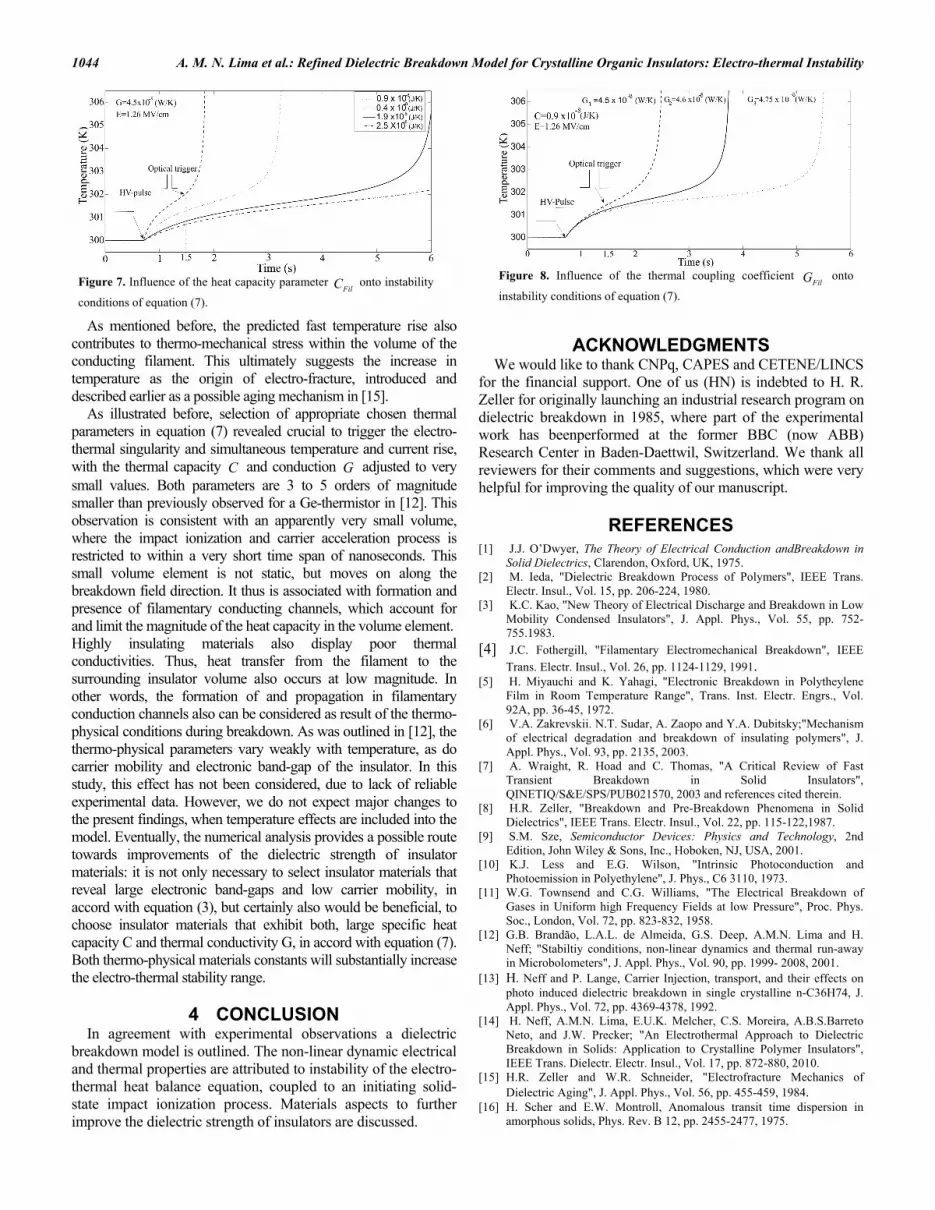
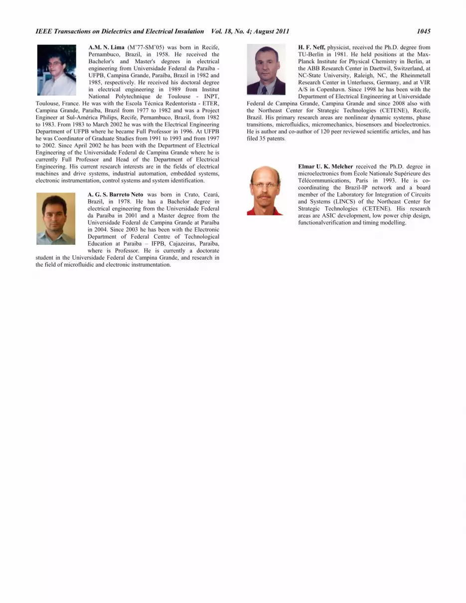
Influence and sensitivity of the selected heat capacity and heat transfer parameters onto instability/stability conditions, pertaining to the solution of equation (7), are illustrated in Figures 7and 8. In both cases, towards higher
FilC , and FilG ,
the pre-breakdown period increases. Stability is maintained as both thermo-physical parameters grow larger.
Nevertheless, in view of the present model, the thermal run-away also can be triggered by other electrical effects that would create fast initial resistance transients. An example is the transient tunneling injection at very high fields. Associated currents temporally and locally reduce the resistance near electrode tips and at surface inhomogeneities.
Figure 6. Influence of bias voltage on breakdown conditions, revealed by the variation of sample temperature as function of time. In the bottom graphic the solution to equation (7) remains stable at (and below) 1.17 and 1.2 MV/cm, but becomes unstable at (and over) 1.26 MV/cm as shown in the top graphic. Switching points of high voltage bias, as well as onset and the use of ),,( tTER InscritIns
,
accounting for optically triggered photo-injection of free carriers, are indicated.
1044 A. M. N. Lima et al.: Refined Dielectric Breakdown Model for Crystalline Organic Insulators: Electro-thermal Instability
As mentioned before, the predicted fast temperature rise also contributes to thermo-mechanical stress within the volume of the conducting filament. This ultimately suggests the increase in temperature as the origin of electro-fracture, introduced and described earlier as a possible aging mechanism in [15].
As illustrated before, selection of appropriate chosen thermal parameters in equation (7) revealed crucial to trigger the electro-thermal singularity and simultaneous temperature and current rise, with the thermal capacity C and conduction G adjusted to very small values. Both parameters are 3 to 5 orders of magnitude smaller than previously observed for a Ge-thermistor in [12]. This observation is consistent with an apparently very small volume, where the impact ionization and carrier acceleration process is restricted to within a very short time span of nanoseconds. This small volume element is not static, but moves on along the breakdown field direction. It thus is associated with formation and presence of filamentary conducting channels, which account for and limit the magnitude of the heat capacity in the volume element. Highly insulating materials also display poor thermal conductivities. Thus, heat transfer from the filament to the surrounding insulator volume also occurs at low magnitude. In other words, the formation of and propagation in filamentary conduction channels also can be considered as result of the thermo-physical conditions during breakdown. As was outlined in [12], the thermo-physical parameters vary weakly with temperature, as do carrier mobility and electronic band-gap of the insulator. In this study, this effect has not been considered, due to lack of reliable experimental data. However, we do not expect major changes to the present findings, when temperature effects are included into the model. Eventually, the numerical analysis provides a possible route towards improvements of the dielectric strength of insulator materials: it is not only necessary to select insulator materials that reveal large electronic band-gaps and low carrier mobility, in accord with equation (3), but certainly also would be beneficial, to choose insulator materials that exhibit both, large specific heat capacity C and thermal conductivity G, in accord with equation (7). Both thermo-physical materials constants will substantially increase the electro-thermal stability range.
4 CONCLUSION In agreement with experimental observations a dielectric
breakdown model is outlined. The non-linear dynamic electrical and thermal properties are attributed to instability of the electro-thermal heat balance equation, coupled to an initiating solid-state impact ionization process. Materials aspects to further improve the dielectric strength of insulators are discussed.
ACKNOWLEDGMENTS
We would like to thank CNPq, CAPES and CETENE/LINCS for the financial support. One of us (HN) is indebted to H. R. Zeller for originally launching an industrial research program on dielectric breakdown in 1985, where part of the experimental work has beenperformed at the former BBC (now ABB) Research Center in Baden-Daettwil, Switzerland. We thank all reviewers for their comments and suggestions, which were very helpful for improving the quality of our manuscript.
REFERENCES [1] J.J. O’Dwyer, The Theory of Electrical Conduction andBreakdown in
Solid Dielectrics, Clarendon, Oxford, UK, 1975. [2] M. Ieda, "Dielectric Breakdown Process of Polymers", IEEE Trans.
Electr. Insul., Vol. 15, pp. 206-224, 1980. [3] K.C. Kao, "New Theory of Electrical Discharge and Breakdown in Low
Mobility Condensed Insulators", J. Appl. Phys., Vol. 55, pp. 752-755.1983.
[4] J.C. Fothergill, "Filamentary Electromechanical Breakdown", IEEE
Trans. Electr. Insul., Vol. 26, pp. 1124-1129, 1991. [5] H. Miyauchi and K. Yahagi, "Electronic Breakdown in Polytheylene
Film in Room Temperature Range", Trans. Inst. Electr. Engrs., Vol. 92A, pp. 36-45, 1972.
[6] V.A. Zakrevskii. N.T. Sudar, A. Zaopo and Y.A. Dubitsky;"Mechanism of electrical degradation and breakdown of insulating polymers", J. Appl. Phys., Vol. 93, pp. 2135, 2003.
[7] A. Wraight, R. Hoad and C. Thomas, "A Critical Review of Fast Transient Breakdown in Solid Insulators", QINETIQ/S&E/SPS/PUB021570, 2003 and references cited therein.
[8] H.R. Zeller, "Breakdown and Pre-Breakdown Phenomena in Solid Dielectrics", IEEE Trans. Electr. Insul., Vol. 22, pp. 115-122,1987.
[9] S.M. Sze, Semiconductor Devices: Physics and Technology, 2nd Edition, John Wiley & Sons, Inc., Hoboken, NJ, USA, 2001.
[10] K.J. Less and E.G. Wilson, "Intrinsic Photoconduction and Photoemission in Polyethylene", J. Phys., C6 3110, 1973.
[11] W.G. Townsend and C.G. Williams, "The Electrical Breakdown of Gases in Uniform high Frequency Fields at low Pressure", Proc. Phys. Soc., London, Vol. 72, pp. 823-832, 1958.
[12] G.B. Brandão, L.A.L. de Almeida, G.S. Deep, A.M.N. Lima and H. Neff; "Stabiltiy conditions, non-linear dynamics and thermal run-away in Microbolometers", J. Appl. Phys., Vol. 90, pp. 1999- 2008, 2001.
[13] H. Neff and P. Lange, Carrier Injection, transport, and their effects on photo induced dielectric breakdown in single crystalline n-C36H74, J. Appl. Phys., Vol. 72, pp. 4369-4378, 1992.
[14] H. Neff, A.M.N. Lima, E.U.K. Melcher, C.S. Moreira, A.B.S.Barreto Neto, and J.W. Precker; "An Electrothermal Approach to Dielectric Breakdown in Solids: Application to Crystalline Polymer Insulators", IEEE Trans. Dielectr. Electr. Insul., Vol. 17, pp. 872-880, 2010.
[15] H.R. Zeller and W.R. Schneider, "Electrofracture Mechanics of Dielectric Aging", J. Appl. Phys., Vol. 56, pp. 455-459, 1984.
[16] H. Scher and E.W. Montroll, Anomalous transit time dispersion in amorphous solids, Phys. Rev. B 12, pp. 2455-2477, 1975.
Figure 7. Influence of the heat capacity parameter FilC onto instability
conditions of equation (7).
Figure 8. Influence of the thermal coupling coefficient
FilG onto
instability conditions of equation (7).
IEEE Transactions on Dielectrics and Electrical Insulation Vol. 18, No. 4; August 2011 1045
A.M. N. Lima (M’77-SM’05) was born in Recife, Pernambuco, Brazil, in 1958. He received the Bachelor's and Master's degrees in electrical engineering from Universidade Federal da Paraíba - UFPB, Campina Grande, Paraíba, Brazil in 1982 and 1985, respectively. He received his doctoral degree in electrical engineering in 1989 from Institut National Polytechnique de Toulouse - INPT,
Toulouse, France. He was with the Escola Técnica Redentorista - ETER, Campina Grande, Paraíba, Brazil from 1977 to 1982 and was a Project Engineer at Sul-América Philips, Recife, Pernambuco, Brazil, from 1982 to 1983. From 1983 to March 2002 he was with the Electrical Engineering Department of UFPB where he became Full Professor in 1996. At UFPB he was Coordinator of Graduate Studies from 1991 to 1993 and from 1997 to 2002. Since April 2002 he has been with the Department of Electrical Engineering of the Universidade Federal de Campina Grande where he is currently Full Professor and Head of the Department of Electrical Engineering. His current research interests are in the fields of electrical machines and drive systems, industrial automation, embedded systems, electronic instrumentation, control systems and system identification.
A. G. S. Barreto Neto was born in Crato, Ceará, Brazil, in 1978. He has a Bachelor degree in electrical engineering from the Universidade Federal da Paraíba in 2001 and a Master degree from the Universidade Federal de Campina Grande at Paraíba in 2004. Since 2003 he has been with the Electronic Department of Federal Centre of Technological Education at Paraiba – IFPB, Cajazeiras, Paraiba, where is Professor. He is currently a doctorate
student in the Universidade Federal de Campina Grande, and research in the field of microfluidic and electronic instrumentation.
H. F. Neff, physicist, received the Ph.D. degree from TU-Berlin in 1981. He held positions at the Max-Planck Institute for Physical Chemistry in Berlin, at the ABB Research Center in Daettwil, Switzerland, at NC-State University, Raleigh, NC, the Rheinmetall Research Center in Unterluess, Germany, and at VIR A/S in Copenhavn. Since 1998 he has been with the Department of Electrical Engineering at Universidade
Federal de Campina Grande, Campina Grande and since 2008 also with the Northeast Center for Strategic Technologies (CETENE), Recife, Brazil. His primary research areas are nonlinear dynamic systems, phase transitions, microfluidics, micromechanics, biosensors and bioelectronics. He is author and co-author of 120 peer reviewed scientific articles, and has filed 35 patents.
Elmar U. K. Melcher received the Ph.D. degree in microelectronics from École Nationale Supérieure des Télécommunications, Paris in 1993. He is co-coordinating the Brazil-IP network and a board member of the Laboratory for Integration of Circuits and Systems (LINCS) of the Northeast Center for Strategic Technologies (CETENE). His research areas are ASIC development, low power chip design, functionalverification and timing modelling.