adt7473 dbcool remote thermal monitor and fan control
TRANSCRIPT
© Semiconductor Components Industries, LLC, 2009
April, 2009 − Rev. 61 Publication Order Number:
ADT7473/D
ADT7473
dBCOOL
Remote Thermal
Monitor and Fan Control
The ADT7473/ADT7473−1 dBCOOL controller is a thermalmonitor and multiple PWM fan controller for noise sensitive or powersensitive applications requiring active system cooling. TheADT7473/ADT7473−1 can drive a fan using either a low or highfrequency drive signal, monitor the temperature of up to two remotesensor diodes plus its own internal temperature, and measure andcontrol the speed of up to four fans so they operate at the lowestpossible speed for minimum acoustic noise.
The automatic fan speed control loop optimizes fan speed for agiven temperature. A unique dynamic TMIN control mode enables thesystem thermals/acoustics to be intelligently managed. Theeffectiveness of the system’s thermal solution can be monitored usingthe THERM input. The ADT7473/ADT7473−1 also provide criticalthermal protection to the system using the bidirectional THERM pinas an output to prevent system or component overheating.
FEATURES
• Controls and Monitors Up to 4 Fans
• High and Low Frequency Fan Drive Signal
• 1 On−Chip and 2 Remote Temperature Sensors
• Series Resistance Cancellation on the Remote Channel
• Extended Temperature Measurement Range, Up to 191°C
• Dynamic TMIN Control Mode Intelligently Optimizes SystemAcoustics
• Automatic Fan Speed Control Mode Controls System Cooling Basedon Measured Temperature
• Enhanced Acoustic Mode Dramatically Reduces User Perception ofChanging Fan Speeds
• Thermal Protection Feature via THERM Output
• Monitors Performance Impact of Intel Pentium 4 Processor
• Thermal Control Circuit via THERM Input
• 3−Wire and 4−Wire Fan Speed Measurement
• Limit Comparison of All Monitored Values
• Meets SMBus 2.0 Electrical Specifications(Fully SMBus 1.1 Compliant)
• This is a Pb−Free Device
• Fully RoHS Compliant
MARKING DIAGRAMS
http://onsemi.com
PIN ASSIGNMENTS
# = Pb−Free PackageYYWW = Date Codexx = Assembly Lot
See detailed ordering and shipping information in the packagedimensions section on page 73 of this data sheet.
ORDERING INFORMATION
12
11
10
9
D1–
D2+
D2–
16
15
14
13
SDA
PWM1/XTO
VCCP
D1+
5
6
7
8
TACH1
TACH2
PWM3
1
2
3
4
SCL
GND
VCC
TACH3 ADT7473TOP VIEWPWM2/
SMBALERT
TACH4/GPIO/THERMSMBALERT
12
11
10
9
D1–
D2+
D2–
16
15
14
13
SDA
PWM1/XTO
VCCP
D1+
5
6
7
8
TACH1
TACH2
1
2
3
4
SCL
GND
VCC
TACH3/ADDR SELECT ADT7473−1
TOP VIEWTHERM_LATCH/PWM2
PWM3/ADDREN TACH4/GPIO/THERMSMBALERT
ADT7473ARQZ#YYWW
xxxx
QSOP−16CASE 492
ADT7473 ADT7473−1
ADT7473−1ARQZxxxx
ADT7473
http://onsemi.com2
Figure 1. Functional Block Diagram
BAND GAPREFERENCE
10−BITADC
VALUE ANDLIMIT
REGISTERS
LIMITCOMPARATORS
INTERRUPTSTATUS
REGISTERS
GND
PWM1
PWM2
PWM3
PWMREGISTERS
ANDCONTROLLERS
(HF AND LF)
ACOUSTICENHANCEMENT
CONTROL
SMBusADDRESS
SELECTION
AUTOMATICFAN SPEEDCONTROL
DYNAMICTMIN
CONTROLTACH1TACH2TACH3TACH4
FANSPEED
COUNTER
THERMALPROTECTION
PERFORMANCEMONITORING
*THERM_LATCH
INPUTSIGNAL
CONDITIONINGAND
ANALOGMULTIPLEXER
VCC TO ADT7473/ADT7473−1
VCC
D1+
D1–
D2+
D2–
VCCP
BAND GAPTEMP SENSOR
SRC
INTERRUPTMASKING
PWMCONFIGURATION
REGISTERS
ADDRESSPOINTER
REGISTER
SERIAL BUSINTERFACE
SCL*ADDR SELECT*ADDREN SDA SMBALERT
ADT7473/ADT7473−1
*PIN FUNCTION ONLY AVAILABLE ON THE ADT7473−1
ABSOLUTE MAXIMUM RATINGS
Parameter Rating Unit
Positive Supply Voltage (VCC) 3.6 V
Voltage on any Input or Output Pin −0.3 to +3.6 V
Input Current at any Pin ±5.0 mA
Package Input Current ±20 mA
Maximum Junction Temperature (TJ max) 150 °C
Storage Temperature Range −65 to +150 °C
Lead Temperature, SolderingIR Reflow Peak TemperatureLead Temperature (Soldering, 10 sec)
260300
°C
ESD Rating 1500 V
Stresses exceeding Maximum Ratings may damage the device. Maximum Ratings are stress ratings only. Functional operation above theRecommended Operating Conditions is not implied. Extended exposure to stresses above the Recommended Operating Conditions may affectdevice reliability.
NOTE: This device is ESD sensitive. Use standard ESD precautions when handling.
THERMAL CHARACTERISTICS
Package Type JA JC Unit
16−lead QSOP 150 39 °C/W
NOTE: JA is specified for the worst−case conditions, that is, a device soldered in a circuit board for surface−mount packages.
ADT7473
http://onsemi.com3
ELECTRICAL CHARACTERISTICS TA = TMIN to TMAX, VCC = VMIN to VMAX, unless otherwise noted. (Note 1)
Parameter Conditions Min Typ Max Unit
Power Supply
Supply Voltage 3.0 3.3 3.6 V
Supply Current, ICC Interface inactive, ADC active 1.5 3.0 mA
Temperature−to−Digital Converter
Local Sensor Accuracy
Resolution
0°C ≤ TA ≤ 85°C−40°C ≤ TA ≤ +125°C
±0.5
0.25
±1.5±2.5
°C
Remote Diode Sensor Accuracy
Resolution
0°C ≤ TA ≤ 85°C−40°C ≤ TA ≤ +125°C
±0.5
0.25
±1.5±2.5
°C
Remote Sensor Source Current First CurrentSecond CurrentThird Current
63696
A
Analog−to−Digital Converter (Including MUX and Attentuators)
Total Unadjusted Error (TUE) ±1.5 %
Differential Nonlinearity (DNL) 8 bits ±1.0 LSB
Power Supply Sensitivity ±0.1 %/V
Conversion Time (Voltage Input) Averaging enabled 11 ms
Conversion Time (Local Temperature) Averaging enabled 12 ms
Conversion Time (Remote Temperature) Averaging enabled 38 ms
Total Monitoring Cycle Time Averaging enabledAveraging disabled
14519
ms
Input Resistance For VCCP channel 70 120 k
Fan RPM−to−Digital Converter
Accuracy 0°C ≤ TA ≤ 70°C−40°C ≤ TA ≤ +120°C
±6.0±10
%
Full−Scale Count 65,535
Nominal Input RPM Fan count = 0xBFFFFan count = 0x3FFFFan count = 0x0438Fan count = 0x021C
1093295000
10,000
RPM
Open−Drain Digital Outputs, PWM1 to PWM3, XTO
Current Sink, IOL 8.0 mA
Output Low Voltage, VOL IOUT = −8.0 mA 0.4 V
High Level Output Current, IOH VOUT = VCC 0.1 20 A
Open−Drain Serial Data Bus Output (SDA)
Output Low Voltage, VOL IOUT = −4.0 mA 0.4 V
High Level Output Current, IOH VOUT = VCC 0.1 1.0 A
Digital Output Logic Levels, ADT7473−1 (THERM_LATCH) ADTL+
Output High Voltage, VOH 0.75 x VCC V
Output Low Voltage, VOL 0.4 V
SMBus Digital Inputs (SCL, SDA)
Input High Voltage, VIH 2.0 V
Input Low Voltage, VIL 0.4 V
Hysteresis 500 mV
Digital Input Logic Levels (TACH Inputs)
Input High Voltage, VIHMaximum input voltage
2.03.6
V
Input Low Voltage, VILMinimum input voltage −0.3
0.8 V
Hysteresis 0.5 V p−p

ADT7473
http://onsemi.com4
ELECTRICAL CHARACTERISTICS TA = TMIN to TMAX, VCC = VMIN to VMAX, unless otherwise noted. (Note 1)
Parameter UnitMaxTypMinConditions
Digital Input Logic Levels (THERM) ADTL+
Input High Voltage, VIH 0.75 x VCC V
Input Low Voltage, VIL 0.8 V
Input High Voltage, VIH
Input Low Voltage, VIL VIN = VCC ±1 A
Input Low Current, IIL VIN = 0 ±1 A
Input Capacitance, CIN 5.0 pF
Serial Bus Timing (Note 2) (See Figure 2)
Clock Frequency, fSCLK 10 400 kHz
Glitch Immunity, tSW 50 ns
Bus Free Time, tBUF 4.7 s
SCL Low Time, tLOW 4.7 s
SCL High Time, tHIGH 4.0 50 s
SCL, SDA Rise Time, tr 1,000 ns
SCL, SDA Fall Time, tf 300 s
Data Setup Time, tSU; DAT 250 ns
Detect Clock Low Timeout, tTIMEOUT Can be optionally disabled 15 35 ms
1. All voltages are measured with respect to GND, unless otherwise noted. Typicals are at TA = 25°C and represent most likely parametric norm.Logic inputs accept input high voltages up to VMAX, even when the device is operating down to VMIN. Timing specifications are tested at logiclevels of VIL = 0.8 V for a falling edge and VIH = 2.0 V for a rising edge.
2. Serial management bus (SMBus) timing specifications are guaranteed by design and are not production tested.
Figure 2. Serial Bus Timing Diagram
SCL
SDA
P SS PtBUF
tHD: STA tHD: DAT tSU: DAT
tFtRtLOW
tSU: STAtHIGH
tHD: STA
tSU: STO
ADT7473
http://onsemi.com5
PIN ASSIGNMENT
Pin No. Mnemonic Description
1 SCL Digital Input (Open Drain). SMBus serial clock input. Requires SMBus pullup.
2 GND Ground Pin.
3 VCC Power Supply. Powered by 3.3 V.
4 TACH3 Digital Input (Open Drain). Fan tachometer input to measure speed of Fan 3.
ADDR SELECT If in address select mode, the logic state of this pin defines the SMBus device address.
5 PWM2 Digital Output (Open Drain). ADT7473 default pin function is PWM2. Requires 10 k typical pullup.Pulse−width modulated output to control Fan 2 speed. Can be configured as a high or low frequencydrive.
SMBALERT On the ADT7473, this pin can be reconfigured as an SMBALERT interrupt output to signal out−of−limitconditions.
THERM_LATCH ADT7473−1 default pin function. THERM_LATCH is a thermal event alert signal when anovertemperature condition occurs.
6 TACH1 Digital Input (Open Drain). Fan tachometer input to measure speed of Fan 1.
7 TACH2 Digital Input (Open Drain). Fan tachometer input to measure speed of Fan 2.
8 PWM3 Digital I/O (Open Drain). Pulse−width modulated output to control the speed of Fan 3 and Fan 4.Requires 10 k typical pullup. Can be configured as a high or low frequency drive.
ADDREN If pulled low on powerup, the ADT7473−1 enters address select mode, and the state of Pin 4(ADDR SELECT) determines the ADT7473−1 slave address.
9 TACH4 Digital Input (Open Drain). Fan tachometer input to measure speed of Fan 4.
GPIO General Purpose Open Drain Digital I/O.
THERM Bidirectional THERM pin. Can be used to time and monitor assertions on the THERM input as well asto assert when an ADT7473 THERM overtemperature limit is exceeded. For example, the pin can beconnected to the PROCHOT output of an Intel Pentium 4 processor or to the output of a trip pointtemperature sensor. Can be used as an output to signal overtemperature conditions.
SMBALERT Digital Output (Open Drain). This pin can be reconfigured as an SMBALERT interrupt output to signalout−of−limit conditions.
10 D2− Cathode Connection to Second Thermal Diode.
11 D2+ Anode Connection to Second Thermal Diode.
12 D1− Cathode Connection to First Thermal Diode.
13 D1+ Anode Connection to First Thermal Diode.
14 VCCP Analog Input. Monitors processor core voltage (0 V to 3.0 V).
15 PWM1
XTO
Digital Output (Open Drain). Pulse−width modulated output to control Fan 1 speed. Requires 10 ktypical pullup. Also functions as the output from the XNOR tree in XNOR test mode.
16 SDA Digital I/O (Open Drain). SMBus bidirectional serial data. Requires 10 k typical pullup.
ADT7473
http://onsemi.com6
TYPICAL CHARACTERISTICS
Figure 3. Remote Temperature Error vs. PCBResistance
Figure 4. Temperature Error vs. CapacitanceBetween D+ and D−
Figure 5. Remote Temperature Error vs.Common−Mode Noise Frequency
Figure 6. Remote Temperature Error vs.Common−Mode Noise Frequency
Figure 7. Normal IDD vs. Power Supply Figure 8. Internal Temperature Error vs.Frequency
60
0 20 40 60
LEAKAGE RESISTANCE (MΩ)
TE
MP
ER
AT
UR
E E
RR
OR
(C
)
80 10010 30 50 70 90–60
–40
–20
0
20
40
D+ TO GND
D+ TO VCC
0
–10
–20
–30
–40
–50
–600 2 4 6 8 10 12
CAPACITANCE (nF)
TE
MP
ER
AT
UR
E E
RR
OR
(C
)
14 16 18 20 22
1.20
1.18
1.16
1.14
1.12
1.10
1.08
1.06
3.0 3.1 3.2 3.3 3.4VDD (V)
I DD
(m
A)
1.04
1.02
3.5 3.6
1.00
0.98
ADT7473
http://onsemi.com7
TYPICAL CHARACTERISTICS
Figure 9. Remote Temperature Error vs. PowerSupply Noise Frequency
Figure 10. Internal Temperature Error vs.Temperature
Figure 11. Remote Temperature Error vs. Temperature
3.0
2.5
2.0
1.5
1.0
0.5
–40 –20 0 20 40 60 85
OIL BATH TEMPERATURE (C)
TE
MP
ER
AT
UR
E E
RR
OR
(C
)
105 125
3.0
2.5
2.0
1.5
1.0
0.5
0
–0.5
–40 –20 0 20 40 60 85
OIL BATH TEMPERATURE (C)
TE
MP
ER
AT
UR
E E
RR
OR
(C
)
–1.0
–1.5
105 125–2.0
0
0.5
1.0
1.5

ADT7473
http://onsemi.com8
Product DescriptionThe ADT7473/ADT7473−1 is a complete thermal
monitor and multiple fan controller for any system requiringthermal monitoring and cooling. The device communicateswith the system via a serial system management bus. Theserial bus controller has a serial data line for reading andwriting addresses and data (Pin 16), and an input line for theserial clock (Pin 1). All control and programming functionsfor the ADT7473/ADT7473−1 are performed over the serialbus. Additionally, a pin can be reconfigured as anSMBALERT output to signal out−of−limit conditions.
Table 1 illustrates the differences between the ADT7473and the ADT7473−1.
Table 1. ADT7473/ADT7473−1 Device Comparison
Feature ADT7473 ADT7473−1
Pin 5 Default:PWM2
Default:THERM_LATCH
SMBus Address FixedAddress
Address selectable
Remote Ch. 2Therm Limit
= 100°C = 136°C
Register 0x30,0x31, 0x32
Default:0x00
Default: 0xFF
Register 0x3FRevision Reg
Default: 0x68
Default: 0x69
Register 0x40, Bit 7 Reserved (R/W) 1 = Reset Latch(lockable)
Register 0x42, Bit 0 Reserved (Read−only)1 = THERMLimit Latched
Registers 0x5C,0x5D, 0x5E
Default: 0x82
Default: 0x62
Register 0x7C, Bit 4 Reserved THERM OutputHysteresis
Register 0x7D, Bit 4 Reserved THERM_LATCHConfiguration0 = Remote Channel 21 = Remote Channel 1and Remote Channel 2
Comparison Between ADT7467 andADT7473/ADT7473−1
The following list shows some comparisons between theADT7467 and the ADT7473/ADT7473−1:• The ADT7473/ADT7473−1 can be powered via a
3.3 V supply only, and does not support 5.0 Voperation, while the ADT7467 does. Violating thisspecification results in irreversible damage to theADT7473/ADT7473−1. See the Specifications sectionfor more information.
• A high frequency PWM drive can be independentlyselected for each PWM channel on theADT7473/ADT7473−1. This is not available on theADT7467.
• The range and resolution of the temperature offsetregister can be changed from a ±64°C range at 0.5°Cresolution to a ±128°C range at 1°C resolution. This isnot available on the ADT7467.
• THERM overtemperature events can bedisabled/enabled individually on each temperaturechannel. This is not available on the ADT7467.
• Bit 7 of Configuration Register 1 is no longer supportedbecause the ADT7473/ADT7473−1 cannot be poweredvia a 5.0 V supply.
• Bit 0 of Configuration Register 1 (0x40) remainswritable after the lock bit is set. This bit enablesmonitoring.
• 2−wire fan speed measurement is not supported on theADT7473/ADT7473−1.
How to Set the Functionality of Pin 9Pin 9 on the ADT7473/ADT7473−1 has four possible
functions: SMBALERT, THERM, GPIO, and TACH4. Theuser chooses the required functionality by setting Bit 0 andBit 1 of Configuration Register 4 (0x7D).
Table 2. Pin 9 Settings
Bit 0 Bit 1 Function
0 0 TACH4
0 1 THERM
1 0 SMBALERT
1 1 GPIO
Recommended ImplementationConfiguring the ADT7473 as shown in Figure 12 allows
the system designer to use the following features:• Two PWM outputs for fan control of up to three fans.
(The front and rear chassis fans are connected inparallel.)
• Three TACH fan speed measurement inputs.
• VCC measured internally through Pin 3.
• CPU temperature measured using Remote 1temperature channel.
• Ambient temperature measured through Remote 2temperature channel.
• Bidirectional THERM pin. This feature allows IntelPentium 4 PROCHOT monitoring and can function asan overtemperature THERM output. It can alternativelybe programmed as an SMBALERT system interruptoutput.

ADT7473
http://onsemi.com9
Figure 12. ADT7473 Configuration
TACH2
PWM3
TACH3
D1+
D1–
GND
ADT7473
SCL
SDA
TACH1
PWM1
CPU FAN
AMBIENTTEMPERATURE
SMBALERT
D2+
D2–
THERMPROCHOT
FRONTCHASSISFAN
REARCHASSISFAN
CPU
ICH
Serial Bus InterfaceOn PCs and servers, control of the ADT7473/ADT7473−1
is carried out using the SMBus. The ADT7473/ADT7473−1is connected to this bus as a slave device, under the control ofa master controller, which is usually (but not necessarily) theICH.
The ADT7473 has a fixed 7−bit serial bus address of0101110 or 0x2E. The read/write bit must be added to get the8−bit address (01011100 or 0x5C). When the ADT7473−1is powered up with Pin 8 (PWM3/ADDREN) high, theADT7473−1 has a default SMBus address of 0101110 or0x2E. If more than one ADT7473−1 is used in a system,each ADT7473−1 is placed in ADDR SELECT mode bystrapping Pin 8 low on powerup. The logic state of Pin 4 thendetermines the device’s SMBus address. The logic of thesepins is sampled on powerup.
The device address is sampled on powerup and latched onthe first valid SMBus transaction, more precisely on thelow−to−high transition at the beginning of the eighth SCLpulse, when the serial bus address byte matches the selectedslave address. The selected slave address is chosen using theADDREN pin/ADDR SELECT pin. Any attempted changein the address has no effect after this.
Table 3. Hardwiring the ADT7473−1 SMBus DeviceAddress
Pin 13 State Pin 14 State Address
0 Low (10 k to GND) 0101100 (0x2C)
0 High (10 k pullup) 0101101 (0x2D)
1 Don’t care 0101110 (0x2E)
Figure 13. Default SMBus Address = 0x2E
ADT7473−1
4
ADDRESS = 0x2E
VCC
ADDR SELECT
8PWM3/ADDREN
10kΩ
Figure 14. SMBus Address = 0x2C (Pin4 = 0)
ADT7473−1
4
ADDRESS = 0x2C
8
10kΩ
ADDR SELECT
PWM3/ADDREN
Figure 15. SMBus Address = 0x2D (Pin 4 = 1)
ADT7473−1
4
ADDRESS = 0x2D
8
VCC
10kΩ
ADDR SELECT
PWM3/ADDREN

ADT7473
http://onsemi.com10
Figure 16. Unpredictable SMBus Address if Pin 8is Unconnected
DO NOT LEAVE ADDRENUNCONNECTED! CANCAUSE UNPREDICTABLEADDRESSES.
ADT7473−1
4
8 NC
VCC
10kΩ
CARE SHOULD BE TAKEN TO ENSURE THAT PIN 8 (PWM3/ADDREN) IS EITHER TIED HIGH OR LOW. LEAVING PIN 8 FLOATING COULD CAUSE THE ADT7473-1 TO POWER UP WITH AN UNEXPECTED ADDRESS.
NOTE THAT IF THE ADT7473-1 IS PLACED INTO ADDR SELECT MODE, PINS 8 AND 4 CANNOT BE USED AS THE ALTERNATIVE FUNCTIONS (PWM3, TACH4/THERM) UNLESS THE CORRECT CIRCUIT IS MUXED IN AT THE CORRECT TIME OR DESIGNED TO HANDLE THESE DUAL FUNCTIONS.
ADDR SELECT
PWM3/ADDREN
The ability to make hardwired changes to the SMBusslave address allows the user to avoid conflicts with otherdevices sharing the same serial bus, for example, if morethan one ADT7473−1 is used in a system.
Data is sent over the serial bus in sequences of nine clockpulses: eight bits of data followed by an acknowledge bitfrom the slave device. Transitions on the data line mustoccur during the low period of the clock signal and remainstable during the high period because a low−to−hightransition when the clock is high might be interpreted as astop signal. The number of data bytes that can be transmittedover the serial bus in a single read or write operation islimited only by what the master and slave devices canhandle.
When all data bytes have been read or written, stopconditions are established. In write mode, the master pullsthe data line high during the tenth clock pulse to assert a stopcondition. In read mode, the master device overrides theacknowledge bit by pulling the data line high during the lowperiod before the ninth clock pulse; this is known as NoAcknowledge. The master takes the data line low during thelow period before the tenth clock pulse, and then high duringthe tenth clock pulse to assert a stop condition.
Any number of bytes of data can be transferred over theserial bus in one operation, but it is not possible to mix readand write in one operation, because the type of operation isdetermined at the beginning and cannot subsequently bechanged without starting a new operation.
In the ADT7473/ADT7473−1, write operations containeither one or two bytes, and read operations contain onebyte. To write data to one of the device data registers or readdata from it, the address pointer register must be set so thecorrect data register is addressed, and then data can bewritten into that register or read from it. The first byte of awrite operation always contains an address that is stored inthe address pointer register. If data is written to the device,the write operation contains a second data byte that is writtento the register selected by the address pointer register.
This write operation is shown in Figure 17. The deviceaddress is sent over the bus, and then R/W is set to 0. Thisis followed by two data bytes. The first data byte is theaddress of the internal data register to be written to, whichis stored in the address pointer register. The second data byteis the data to be written to the internal data register.
When reading data from a register, there are twopossibilities:• If the ADT7473/ADT7473−1’s address pointer register
value is unknown or not the desired value, it must firstbe set to the correct value before data can be read fromthe desired data register. This is done by performing awrite to the ADT7473/ADT7473−1, but only the databyte containing the register address is sent, because nodata is written to the register. This is shown inFigure 18.A read operation is then performed consisting of theserial bus address, R/W bit set to 1, followed by thedata byte read from the data register. This is shown inFigure 19.
• If the address pointer register is known to be already atthe desired address, data can be read from thecorresponding data register without first writing to theaddress pointer register, as shown in Figure 19.
R/W0
SCL
SDA 1 0 1 1 1 0 D7 D6 D5 D4 D3 D2 D1 D0
ACK. BYADT7473/ADT7473−1
START BYMASTER
1 9 1
ACK. BYADT7473/ADT7473−1
9
D7 D6 D5 D4 D3 D2 D1 D0
STOP BYMASTER
1 9
SCL (CONTINUED)
SDA (CONTINUED)
FRAME 1SERIAL BUS ADDRESS BYTE
FRAME 2ADDRESS POINTER REGISTER BYTE
FRAME 3DATA BYTE
ACK. BYADT7473/ADT7473−1
Figure 17. Writing a Register Address to the Address Pointer Register, then Writing Data to the Selected Register

ADT7473
http://onsemi.com11
R/W0
SCL
SDA 1 0 1 1 1 0 D7 D6 D5 D4 D3 D2 D1 D0
STOP BYMASTER
START BYMASTER
FRAME 1SERIAL BUS ADDRESS BYTE
FRAME 2ADDRESS POINTER REGISTER BYTE
1 19
ACK. BYADT7473/ADT7473−1
9
ACK. BYADT7473/ADT7473−1
Figure 18. Writing to the Address Pointer Register Only
Figure 19. Reading Data from a Previously Selected Register
R/W0
SCL
SDA 1 0 1 1 1 0 D7 D6 D5 D4 D3 D2 D1 D0
NO ACK. BYMASTER
STOP BYMASTER
START BYMASTER
FRAME 1SERIAL BUS ADDRESS BYTE
FRAME 2DATA BYTE FROM ADT7473
1 19
ACK. BYADT7473/ADT7473−1
9
It is possible to read a data byte from a data registerwithout first writing to the address pointer register, if theaddress pointer register is already at the correct value.However, it is not possible to write data to a register withoutwriting to the address pointer register, because the first databyte of a write is always written to the address pointerregister.
In addition to supporting the send byte and receive byteprotocols, the ADT7473/ADT7473−1 also supports the readbyte protocol. (See System Management Bus (SMBus)Specifications Version 2 for more information; thisdocument is available from Intel.)
If several read or write operations must be performed insuccession, the master can send a repeat start conditioninstead of a stop condition to begin a new operation.
Write OperationsThe SMBus specification defines several protocols for
various read and write operations. The ADT7473/ADT7473−1 uses the following SMBus write protocols. Thefollowing abbreviations are used in the diagrams:
S—StartP—StopR—ReadW—WriteA—AcknowledgeA—No Acknowledge
Send ByteIn this operation, the master device sends a single
command byte to a slave device, as follows:1. The master device asserts a start condition on
SDA.2. The master sends the 7−bit slave address followed
by the write bit (active low).3. The addressed slave device asserts ACK on SDA.4. The master sends a command code.5. The slave asserts ACK on SDA.
6. The master asserts a stop condition on SDA andthe transaction ends.
For the ADT7473/ADT7473−1, the send byte protocol isused to write a register address to RAM for a subsequentsingle−byte read from the same address. This operation isillustrated in Figure 20.
Figure 20. Setting a Register Address forSubsequent Read
SLAVEADDRESS
W AS A PREGISTERADDRESS
2 31 5 64
If the master is required to read data from the registerimmediately after setting up the address, it can assert a repeatstart condition immediately after the final ACK and carryout a single−byte read without asserting an intermediate stopcondition.
Write ByteIn this operation, the master device sends a command byte
and one data byte to the slave device, as follows:1. The master device asserts a start condition on SDA.2. The master sends the 7−bit slave address followed
by the write bit (active low).3. The addressed slave device asserts ACK on SDA.4. The master sends a command code.5. The slave asserts ACK on SDA.6. The master sends a data byte.7. The slave asserts ACK on SDA.8. The master asserts a stop condition on SDA, and
the transaction ends.The single byte write operation is illustrated in Figure 21.
Figure 21. Single−Byte Write to a Register
SLAVEADDRESS W A DATAS A A PREGISTER
ADDRESS
2 31 5 6 7 84

ADT7473
http://onsemi.com12
Read OperationsThe ADT7473/ADT7473−1 uses the following SMBus
read protocols.
Receive ByteThis operation is useful when repeatedly reading a single
register. The register address must have been previously setup. In this operation, the master device receives a single bytefrom a slave device, as follows:
1. The master device asserts a start condition onSDA.
2. The master sends the 7−bit slave address followedby the read bit (high).
3. The addressed slave device asserts ACK on SDA.4. The master receives a data byte.5. The master asserts NO ACK on SDA.6. The master asserts a stop condition on SDA, and
the transaction ends.In the ADT7473/ADT7473−1, the receive byte protocol
is used to read a single byte of data from a register whoseaddress has previously been set by a send byte or write byteoperation. This operation is illustrated in Figure 22.
Figure 22. Single−Byte Read from a Register
SLAVEADDRESS DATAARS A P
2 431 5 6
Alert Response AddressAlert response address (ARA) is a feature of SMBus
devices that allows an interrupting device to identify itselfto the host when multiple devices exist on the same bus.
The SMBALERT output can be used as either an interruptoutput or an SMBALERT. One or more outputs can beconnected to a common SMBALERT line connected to themaster. If a device’s SMBALERT line goes low, thefollowing events occur:• SMBALERT is pulled low.
• The master initiates a read operation and sends the alertresponse address (ARA = 0001 100). This is a generalcall address that must not be used as a specific deviceaddress.
• The device whose SMBALERT output is low respondsto the alert response address, and the master reads itsdevice address. The address of the device is now knownand can be interrogated in the usual way.
• If more than one device’s SMBALERT output is low,the one with the lowest device address has priority inaccordance with normal SMBus arbitration.
Once the ADT7473/ADT7473−1 has responded to thealert response address, the master must read the statusregisters, and the SMBALERT is cleared only if the errorcondition is gone.
SMBus TimeoutThe ADT7473/ADT7473−1 includes an SMBus timeout
feature. If there is no SMBus activity for 35 ms, theADT7473/ADT7473−1 assumes the bus is locked andreleases the bus. This prevents the device from locking orholding the SMBus expecting data. Some SMBuscontrollers cannot work with the SMBus timeout feature, soit can be disabled.
Configuration Register 1 (0x40)
Bit 6, TODIS = 0; SMBus timeout enabled (default)
Bit 6, TODIS = 1; SMBus timeout disabled
Voltage Measurement InputThe ADT7473/ADT7473−1 has one external voltage
measurement channel and can also measure its own supplyvoltage, VCC. Pin 14 can measure VCCP. The VCC supplyvoltage measurement is carried out through the VCC pin(Pin 3). The VCCP input can be used to monitor a chipsetsupply voltage in computer systems.
Analog−to−Digital ConverterAll analog inputs are multiplexed into the on−chip,
successive approximation, analog−to−digital converter.(ADC) This has a resolution of 10 bits. The basic input rangeis 0 V to 2.25 V, but the input has built−in attenuators to allowmeasurement of VCCP without any external components. Toallow for the tolerance of the supply voltage, the ADCproduces an output of 3/4 full scale (768 decimal or 300hexadecimal) for the nominal input voltage and thus hasadequate headroom to deal with overvoltages.
Input CircuitryThe internal structure for the VCCP analog input is shown
in Figure 23. The input circuit consists of an input protectiondiode, an attenuator, plus a capacitor to form a first orderlow−pass filter that provides the input immunity to highfrequency noise.
Figure 23. Structure of Analog Inputs
VCCP17.5kΩ
52.5kΩ 35pF
Voltage Measurement Registers
Register 0x21, VCCP Reading = 0x00 default
Register 0x22, VCC Reading = 0x00 default
VCCP Limit RegistersAssociated with the VCCP measurement channel is a high
and low limit register. Exceeding the programmed high orlow limit causes the appropriate status bit to be set.Exceeding either limit can also generate SMBALERTinterrupts.
Register 0x46, VCCP Low Limit = 0x00 default
Register 0x47, VCCP High Limit = 0xFF default
ADT7473
http://onsemi.com13
Table 5 shows the input ranges of the analog inputs andoutput codes of the 10−bit ADC.
When the ADC is running, it samples and converts avoltage input in 711 s and averages 16 conversions toreduce noise; a measurement takes nominally 11.38 ms.
Additional ADC Functions for Voltage MeasurementsA number of other functions are available on the
ADT7473/ADT7473−1 to offer the system designerincreased flexibility.
Turn−Off AveragingFor each voltage measurement read from a value register,
16 readings have actually been made internally and theresults averaged before being placed into the value register.When faster conversions are needed, setting Bit 4 ofConfiguration Register 2 (0x73) turns averaging off. Thiseffectively gives a reading 16 times faster (711 s), but thereading may be noisier.
Bypass Voltage Input AttenuatorSetting Bit 5 of Configuration Register 2 (0x73) removes
the attenuation circuitry from the VCCP input. This allowsthe user to directly connect external sensors or to rescale theanalog voltage measurement inputs for other applications.The input range of the ADC without the attenuators is 0 Vto 2.25 V.
Single−Channel ADC ConversionSetting Bit 6 of Configuration Register 2 (0x73) places the
ADT7473/ADT7473−1 into single−channel ADCconversion mode. In this mode, the ADT7473/ADT7473−1can be made to read a single voltage channel only. If theinternal ADT7473/ADT7473−1 clock is used, the selectedinput is read every 711 s. The appropriate ADC channel isselected by writing to Bits [7:5] of the TACH1 minimumhigh byte register (0x55).
Table 4. Programming Single−Channel ADC Mode
Bits [7:5], Register 0x55 Channel Selected
001 VCCP
010 VCC
101 Remote 1 temperature
110 Local temperature
111 Remote 2 temperature
Configuration Register 2 (0x73)
Bit 4 = 1; averaging off.
Bit 5 = 1; bypass input attenuators.
Bit 6 = 1; single−channel convert mode.
TACH1 Minimum High Byte Register (0x55)
Bits [7:5] select ADC channel for single−channel convertmode.

ADT7473
http://onsemi.com14
Table 5. 10−Bit ADC Output Code vs. VIN
ADC Output
VCC (3.3 VIN) (Note 3) VCCP Decimal Binary (10 Bits)
<0.0042 <0.00293 0 00000000 00
0.0042 to 0.0085 0.0293 to 0.0058 1 00000000 01
0.0085 to 0.0128 0.0058 to 0.0087 2 00000000 10
0.0128 to 0.0171 0.0087 to 0.0117 3 00000000 11
0.0171 to 0.0214 0.0117 to 0.0146 4 00000001 00
0.0214 to 0.0257 0.0146 to 0.0175 5 00000001 01
0.0257 to 0.0300 0.0175 to 0.0205 6 00000001 10
0.0300 to 0.0343 0.0205 to 0.0234 7 00000001 11
0.0343 to 0.0386 0.0234 to 0.0263 8 00000010 00
− − − −
1.100 to 1.1042 0.7500 to 0.7529 256 (1/4 scale) 01000000 00
− − − −
2.200 to 2.2042 1.5000 to 1.5029 512 (1/2 scale) 10000000 00
− − − −
3.300 to 3.3042 2.2500 to 2.2529 768 (3/4 scale) 11000000 00
− − − −
4.3527 to 4.3570 2.9677 to 2.9707 1013 11111101 01
4.3570 to 4.3613 2.9707 to 2.9736 1014 11111101 10
4.3613 to 4.3656 2.9736 to 2.9765 1015 11111101 11
4.3656 to 4.3699 2.9765 to 2.9794 1016 11111110 00
4.3699 to 4.3742 2.9794 to 2.9824 1017 11111110 01
4.3742 to 4.3785 2.9824 to 2.9853 1018 11111110 10
4.3785 to 4.3828 2.9853 to 2.9882 1019 11111110 11
4.3828 to 4.3871 2.9882 to 2.9912 1020 11111111 00
4.3871 to 4.3914 2.9912 to 2.9941 1021 11111111 01
4.3914 to 4.3957 2.9941 to 2.9970 1022 11111111 10
>4.3957 >2.9970 1023 11111111 11
3. The VCC output codes listed assume that VCC is 3.3 V.
Temperature Measurement MethodA simple method of measuring temperature is to exploit
the negative temperature coefficient of a diode, measuringthe base−emitter voltage (VBE) of a transistor operated atconstant current. Unfortunately, this technique requirescalibration to null out the effect of the absolute value ofVBE, which varies from device to device.
The technique used in the ADT7473/ADT7473−1measures the change in VBE when the device is operated atthree different currents. Previous devices have used onlytwo operating currents, but the use of a third current allowsautomatic cancellation of resistances in series with theexternal temperature sensor.
Figure 24 shows the input signal conditioning used tomeasure the output of an external temperature sensor. Thisfigure shows the external sensor as a substrate transistor, butit could equally be a discrete transistor. If a discretetransistor is used, the collector is not grounded and shouldbe linked to the base. To prevent ground noise frominterfering with the measurement, the more negativeterminal of the sensor is not referenced to ground, but isbiased above ground by an internal diode at the D− input. C1can optionally be added as a noise filter (recommendedmaximum value 1000 pF). However, a better option in noisyenvironments is to add a filter, as described in the NoiseFiltering section.

ADT7473
http://onsemi.com15
Local Temperature MeasurementThe ADT7473/ADT7473−1 contains an on−chip band
gap temperature sensor whose output is digitized by theon−chip 10−bit ADC. The 8−bit MSB temperature data isstored in the local temperature register (0x26). Because bothpositive and negative temperatures can be measured, thetemperature data is stored in Offset 64 format or twoscomplement format, as shown in Table 10 and Table 11.Theoretically, the temperature sensor and ADC can measuretemperatures from −63°C to +127°C (or −63°C to +191°C inthe extended temperature range) with a resolution of+0.25°C. However, this exceeds the operating temperaturerange of the device, so local temperature measurementsoutside the ADT7473/ADT7473−1 operating temperaturerange are not possible.
Table 6. Twos Complement Temperature Data Format
Temperature Digital Output (10−Bit) (Note 1)
–128°C 1000 0000 00 (diode fault)
–63°C 1100 0001 00
–50°C 1100 1110 00
–25°C 1110 0111 00
–10°C 1111 0110 00
0°C 0000 0000 00
10.25°C 0000 1010 01
25.5°C 0001 1001 10
50.75°C 0011 0010 11
75°C 0100 1011 00
100°C 0110 0100 00
125°C 0111 1101 00
127°C 0111 1111 00
1. Bold numbers denote 2 LSBs of measurement in the ExtendedResolution Register 2 (Register 0x77) with 0.25°C resolution.
Table 7. Extended Range, Temperature Data Format
Temperature Digital Output (10−Bit) (Note 1)
–64°C 0000 0000 00 (diode fault)
–63°C 0000 0001 00
–1°C 0011 1111 00
0°C 0100 0000 00
1°C 0100 0001 00
10°C 0100 1010 00
25°C 0101 1001 00
50°C 0111 0010 00
75°C 1000 1001 00
100°C 1010 0100 00
125°C 1011 1101 00
191°C 1111 1111 00
1. Bold numbers denote 2 LSBs of measurement in the ExtendedResolution Register 2 (Register 0x77) with 0.25°C resolution.
Remote Temperature MeasurementThe ADT7473/ADT7473−1 can measure the temperature
of two remote diode sensors or diode−connected transistorsconnected to Pin 10 and Pin 11 or to Pin 12 and Pin 13.
The forward voltage of a diode or diode−connectedtransistor operated at a constant current exhibits a negativetemperature coefficient of about −2 mV/°C. Unfortunately,the absolute value of VBE varies from device to device andindividual calibration is required to null this out, so thetechnique is unsuitable for mass production. The techniqueused in the ADT7473/ADT7473−1 is to measure the changein VBE when the device is operated at three differentcurrents. This is given by:
VBE = kT/q x ln(N)
where:k is Boltzmann’s constant.T is the absolute temperature in Kelvin.q is the charge on the carrier.N is the ratio of the two currents.
Figure 24 shows the input signal conditioning used tomeasure the output of a remote temperature sensor. Thisfigure shows the external sensor as a substrate transistor,provided for temperature monitoring on some micro−processors. It could also be a discrete transistor such as a2N3904/2N3906.

ADT7473
http://onsemi.com16
Figure 24. Signal Conditioning for Remote Diode Temperature Sensors
D+
VDD
TO ADC
VOUT+
VOUT–
REMOTESENSING
TRANSISTOR
D–
I N1 IN2 I IBIAS
LPF
fC = 65kHz
If a discrete transistor is used, the collector is not groundedand should be linked to the base. If a PNP transistor is used,the base is connected to the D– input and the emitter isconnected to the D+ input. If an NPN transistor is used, theemitter is connected to the D– input and the base isconnected to the D+ input. Figure 25 and Figure 26 showhow to connect the ADT7473/ADT7473−1 to an NPN orPNP transistor for temperature measurement. To preventground noise from interfering with the measurement, themore negative terminal of the sensor is not referenced toground, but is biased above ground by an internal diode atthe D– input.
Figure 25. Measuring Temperature Using an NPNTransistor
2N3904NPN D+
D–
ADT7473/ADT7473−1
Figure 26. Measuring Temperature Using a PNPTransistor
2N3906PNP
ADT7473/ADT7473−1
D+
D–
To measure VBE, the operating current through thesensor is switched among three related currents. N1 x I andN2 x I are different multiples of the current I, as shown inFigure 24. The currents through the temperature diode areswitched between I and N1 x I, giving VBE1, and thenbetween I and N2 x I, giving VBE2. The temperature canthen be calculated using the two VBE measurements. Thismethod can also cancel the effect of any series resistance onthe temperature measurement.
The resulting VBE waveforms are passed through a65 kHz low−pass filter to remove noise and then to achopper−stabilized amplifier. This amplifies and rectifiesthe waveform to produce a dc voltage proportional to VBE.The ADC digitizes this voltage, and a temperature
measurement is produced. To reduce the effects of noise,digital filtering is performed by averaging the results of 16measurement cycles.
The results of remote temperature measurements arestored in 10−bit, twos complement format, as listed in Table10. The extra resolution for the temperature measurementsis held in the Extended Resolution Register 2 (0x77). Thisgives temperature readings with a resolution of 0.25°C.
Noise FilteringFor temperature sensors operating in noisy environments,
previous practice was to place a capacitor across the D+ pinand the D− pin to help combat the effects of noise. However,large capacitances affect the accuracy of the temperaturemeasurement, leading to a recommended maximumcapacitor value of 1000 pF. This capacitor reduces the noise,but does not eliminate it, making use of the sensor difficultin a very noisy environment.
The ADT7473/ADT7473−1 has a major advantage overother devices for eliminating the effects of noise on theexternal sensor. Using the series resistance cancellationfeature, a filter can be constructed between the externaltemperature sensor and the part. The effect of any filterresistance seen in series with the remote sensor isautomatically canceled from the temperature result.
The construction of a filter allows the ADT7473/ADT7473−1 and the remote temperature sensor to operatein noisy environments. Figure 27 shows a low−pass R−Cfilter with the following values:
R 100 , C 1 nF (eq. 1)
This filtering reduces both common−mode noise anddifferential noise.
Figure 27. Filter Between Remote Sensor andADT7473/ADT7473−1
D+
1nF
100Ω
REMOTETEMPERATURE
SENSOR
D–100Ω
Series Resistance CancellationParasitic resistance to the ADT7473/ADT7473−1 D+ and
D− inputs (seen in series with the remote diode) is caused bya variety of factors including PCB track resistance and track

ADT7473
http://onsemi.com17
length. This series resistance appears as a temperature offsetin the remote sensor’s temperature measurement. This errortypically causes a 0.5°C offset per of parasitic resistancein series with the remote diode.
The ADT7473/ADT7473−1 automatically cancels out theeffect of this series resistance on the temperature reading,giving a more accurate result without the need for usercharacterization of this resistance. The ADT7473/ADT7473−1 is designed to automatically cancel up to 3 kof resistance, typically. This is transparent to the user byusing an advanced temperature measurement method. Thisfeature allows resistances to be added to the sensor path toproduce a filter, allowing the part to be used in noisyenvironments. See the Noise Filtering section for details.
Factors Affecting Diode Accuracy
Remote Sensing DiodeThe ADT7473/ADT7473−1 is designed to work with
either substrate transistors built into processors or discretetransistors. Substrate transistors are generally PNP types withthe collector connected to the substrate. Discrete types can beeither PNP or NPN transistors connected as a diode(base−shorted to the collector). If an NPN transistor is used,the collector and base are connected to D+ and the emitter isconnected to D−. If a PNP transistor is used, the collector andbase are connected to D− and the emitter is connected to D+.
To reduce the error due to variations in both substrate anddiscrete transistors, a number of factors should be taken intoconsideration:• The ideality factor, nf, of the transistor is a measure of
the deviation of the thermal diode from ideal behavior.The ADT7473/ADT7473−1 is trimmed for an nf valueof 1.008. Use the following equation to calculate theerror introduced at a temperature, T(°C), when using atransistor whose nf does not equal 1.008. Refer to thedata sheet for the related CPU to obtain the nf values.
(eq. 2)T nf 1.0081.008 273.15 K T
To factor this in, the user can write the T value to the offsetregister. Then, the ADT7473/ADT7473−1 automaticallyadds it to or subtracts it from the temperature measurement.• Some CPU manufacturers specify the high and low
current levels of the substrate transistors. The highcurrent level of the ADT7473/ADT7473−1, IHIGH, is96 A and the low level current, ILOW, is 6 A. If theADT7473/ADT7473−1 current levels do not match thecurrent levels specified by the CPU manufacturer, itmight be necessary to remove an offset. The CPU’sdata sheet advises whether this offset needs to beremoved and how to calculate it. This offset can beprogrammed to the offset register. It is important tonote that, if more than one offset must be considered,the algebraic sum of these offsets must be programmedto the offset register.
If a discrete transistor is used with the ADT7473/ADT7473−1, the best accuracy is obtained by choosingdevices according to the following criteria:• Base−emitter voltage greater than 0.25 V at 6 A, at the
highest operating temperature• Base−emitter voltage less than 0.95 V at 100 A, at the
lowest operating temperature• Base resistance less than 100
• Small variation in hFE (such as 50 to 150) that indicatestight control of VBE characteristics
Transistors, such as 2N3904, 2N3906, or equivalents inSOT−23 packages, are suitable devices to use.
Nulling Out Temperature ErrorsAs CPUs run faster, it becomes more difficult to avoid
high frequency clocks when routing the D+/D– tracesaround a system board. Even when recommended layoutguidelines are followed, some temperature errors can still beattributable to noise coupled onto the D+/D– lines. Constanthigh frequency noise usually attenuates or increasestemperature measurements by a linear, constant value.
The ADT7473/ADT7473−1 has temperature offsetregisters at Register 0x70 and Register 0x72 for theRemote 1 and Remote 2 temperature channels. Byperforming a one−time calibration of the system, the usercan determine the offset caused by system board noise andnull it out using the offset registers. The offset registersautomatically add a twos complement, 8−bit reading toevery temperature measurement. The LSBs add +0.5°Coffset to the temperature reading so the 8−bit registereffectively allows temperature offsets of up to ±64°C witha resolution of +0.5°C. This ensures that the readings in thetemperature measurement registers are as accurate aspossible.
Temperature Offset Registers
Register 0x70, Remote 1 Temperature Offset = 0x00(0°C default)
Register 0x71, Local Temperature Offset = 0x00(0°C default)
Register 0x72, Remote 2 Temperature Offset = 0x00(0°C default)
ADT7460/ADT7473/ADT7473−1Backwards−Compatible Mode
By setting Bit 1 of Configuration Register 5 (0x7C), alltemperature measurements are stored in the zonetemperature value registers (Register 0x25, Register 0x26,and Register 0x27) in twos complement, in the range −63°Cto +127°C. (The ADT7473/ADT7473−1 still makescalculations based on the Offset 64 extended range andclamps the results, if necessary.) The temperature limitsmust be reprogrammed in twos complement. If a twoscomplement temperature below −63°C is entered, the

ADT7473
http://onsemi.com18
temperature is clamped to −63°C. In this mode, the diodefault condition remains −128°C = 1000 0000, while in theextended temperature range (−64°C to +191°C), the faultcondition is represented by −64°C = 0000 0000.
Temperature Measurement Registers
Register 0x25, Remote 1 Temperature
Register 0x26, Local Temperature
Register 0x27, Remote 2 Temperature
Register 0x77, Extended Resolution 2 = 0x00 default
Bits [7:6] TDM2, Remote 2 Temperature LSBs
Bits [5:4] LTMP, Local Temperature LSBs
Bits [3:2] TDM1, Remote 1 Temperature LSBs
Temperature Measurement Limit RegistersAssociated with each temperature measurement channel
are high and low limit registers. Exceeding the programmedhigh or low limit causes the appropriate status bit to be set.Exceeding either limit can also generate SMBALERTinterrupts.
Register 0x4E, Remote 1 Temperature Low Limit = 0x01 default
Register 0x4F, Remote 1 Temperature High Limit = 0x7F default
Register 0x50, Local Temperature Low Limit = 0x01 default
Register 0x51, Local Temperature High Limit = 0x7F default
Register 0x52, Remote 2 Temperature Low Limit = 0x01 default
Register 0x53, Remote 2 Temperature High Limit = 0x7F default
Reading Temperature from the ADT7473/ADT7473−1It is important to note that the temperature can be read
from the ADT7473/ADT7473−1 as an 8−bit value (with 1°Cresolution) or as a 10−bit value (with 0.25°C resolution). Ifonly 1°C resolution is required, the temperature readingscan be read back at any time and in no particular order.
If the 10−bit measurement is required, a 2−register readfor each measurement is used. The extended resolutionregister (Register 0x77) should be read first. This causes alltemperature reading registers to be frozen until alltemperature reading registers have been read from. Thisprevents an MSB reading from being updated while its twoLSBs are being read, and vice versa.
Additional ADC Functions for TemperatureMeasurement
A number of other functions are available on theADT7473/ADT7473−1 to offer the system designerincreased flexibility.
Turn−Off AveragingFor each temperature measurement read from a value
register, 16 readings have actually been made internally andthe results averaged before being placed into the valueregister. Sometimes it is necessary to take a very fastmeasurement. Setting Bit 4 of Configuration Register 2(0x73) turns averaging off.
Table 8. Conversion Time with Averaging Disabled
Channel Measurement Time (ms)
Voltage Channel 0.7
Remote 1 Temperature 7
Remote 2 Temperature 7
Local Temperature 1.3
Table 9. Conversion Time with Averaging Enabled
Channel Measurement Time (ms)
Voltage Channel 11
Remote Temperature 39
Local Temperature 12
Single−Channel ADC ConversionsSetting Bit 6 of Configuration Register 2 (0x73) places the
ADT7473/ADT7473−1 into single−channel ADCconversion mode. In this mode, the ADT7473/ADT7473−1can be made to read a single temperature channel only. Theappropriate ADC channel is selected by writing to Bits [7:5]of the TACH1 minimum high byte register (0x55).
Table 10. Programming Single−Channel ADC Modefor Temperatures
Channel Selected Bits [7:4], Register 0x55
101 Remote 1 Temperature
110 Local Temperature
111 Remote 2 Temperature
Configuration Register 2 (0x73)
Bit 4 = 1, averaging off.
Bit 6 = 1, single−channel convert mode.
TACH1 Minimum High Byte Register (0x55)
Bits [7:5] select the ADC channel for single−channelconvert mode.
Overtemperature EventsOvertemperature events on any of the temperature
channels can be detected and dealt with automatically inautomatic fan speed control mode. Register 0x6A toRegister 0x6C are the THERM limits. When a temperatureexceeds its THERM limit, all PWM outputs run at 100%duty cycle or the maximum PWM duty cycle (Register 0x38,Register 0x39, and Register 0x3A) if Bit 3 of ConfigurationRegister 4 (0x7D) is set. The fans remain running at thisspeed until the temperature drops below THERM minushysteresis; this can be disabled by setting the boost bit inConfiguration Register 3 (0x78), Bit 2. The hysteresis valuefor that THERM limit is the value programmed into thehysteresis registers (Register 0x6D and Register 0x6E). Thedefault hysteresis value is 4°C.

ADT7473
http://onsemi.com19
Figure 28. THERM Limit Operation
FANS
TEMPERATURE
100%
HYSTERESIS (C)
THERM LIMIT
Limits, Status Registers, and Interrupts
Limit ValuesAssociated with each measurement channel on the
ADT7473/ADT7473−1 are high and low limits. These canform the basis of system status monitoring; a status bit canbe set for any out−of−limit condition and is detected bypolling the device. Alternatively, SMBALERT interruptscan be generated to flag a processor or microcontroller ofout−of−limit conditions.
8−Bit LimitsThe following is a list of 8−bit limits on the ADT7473/
ADT7473−1.
Voltage Limit Registers
Register 0x46, VCCP Low Limit = 0x00 default
Register 0x47, VCCP High Limit = 0xFF default
Register 0x48, VCC Low Limit = 0x00 default
Register 0x49, VCC High Limit = 0xFF default
Temperature Limit Registers
Register 0x4E, Remote 1 Temperature Low Limit = 0x01default
Register 0x4F, Remote 1 Temperature High Limit = 0xFFdefault
Register 0x6A, Remote 1 THERM Limit = 0xA4 default
Register 0x50, Local Temperature Low Limit = 0x01 default
Register 0x51, Local Temperature High Limit = 0xFF default
Register 0x6B, Local THERM Temperature Limit = 0xA4default
Register 0x52, Remote 2 Temperature Low Limit = 0x01default
Register 0x53, Remote 2 Temperature High Limit = 0xFFdefault
Register 0x6C, Remote 2 THERM Temperature Limit = 0xA4default
THERM Limit Register
Register 0x7A, THERM Timer Limit = 0x00 default
16−Bit LimitsThe fan TACH measurements are 16−bit results. The fan
TACH limits are also 16 bits, consisting of a high byte andlow byte. Because fans running under speed or stalled are
normally the only conditions of interest, only high limitsexist for fan TACHs. Because the fan TACH period isactually being measured, exceeding the limit indicates aslow or stalled fan.
Fan Limit Registers
Register 0x54, TACH1 Minimum Low Byte = 0xFF default
Register 0x55, TACH1 Minimum High Byte = 0xFF default
Register 0x56, TACH2 Minimum Low Byte = 0xFF default
Register 0x57, TACH2 Minimum High Byte = 0xFF default
Register 0x58, TACH3 Minimum Low Byte = 0xFF default
Register 0x59, TACH3 Minimum High Byte = 0xFF default
Register 0x5A, TACH4 Minimum Low Byte = 0xFF default
Register 0x5B, TACH4 Minimum High Byte = 0xFF default
Out−of−Limit ComparisonsOnce all limits have been programmed, the ADT7473/
ADT7473−1 can be enabled for monitoring. The ADT7473/ADT7473−1 measures all voltage and temperaturemeasurements in round−robin format and sets theappropriate status bit for out−of−limit conditions. TACHmeasurements are not part of this round−robin cycle.Comparisons are done differently depending on whether themeasured value is being compared to a high or low limit.
High limit > comparison performed
Low limit ≤ comparison performedVoltage and temperature channels use a window
comparator for error detecting and, therefore, have high andlow limits. Fan speed measurements use only a low limit.This fan limit is needed only in manual fan control mode.
Analog Monitoring Cycle TimeThe analog monitoring cycle begins when a 1 is written to
the start bit (Bit 0) of Configuration Register 1 (0x40). Bydefault, the ADT7473/ADT7473−1 powers up with this bitset. The ADC measures each analog input in turn and, aseach measurement is completed, the result is automaticallystored in the appropriate value register. This round−robinmonitoring cycle continues unless disabled by writing a 0 toBit 0 of Configuration Register 1.
As the ADC is normally left to free−run in this manner, thetime taken to monitor all the analog inputs is normally notof interest, because the most recently measured value of anyinput can be read out at any time.
For applications where the monitoring cycle time isimportant, it can easily be calculated. The total number ofchannels measured is• One dedicated supply voltage input (VCCP)
• Supply voltage (VCC pin)
• Local temperature
• Two remote temperaturesAs mentioned previously, the ADC performs round−robin
conversions. The total monitoring cycle time for averagedvoltage and temperature monitoring is 146 ms. The total

ADT7473
http://onsemi.com20
monitoring cycle time for voltage and temperaturemonitoring with averaging disabled is 19 ms. The ADT7473/ADT7473−1 is a derivative of the ADT7467. As a result, thetotal conversion time in the ADT7473/ ADT7473−1 is thesame as the total conversion time of the ADT7467, eventhough the ADT7473/ADT7473−1 has fewer monitoredchannels.
Fan TACH measurements are made in parallel and are notsynchronized with the analog measurements in any way.
Interrupt Status RegistersThe results of limit comparisons are stored in Interrupt
Status Register 1 and Interrupt Status Register 2. The statusregister bit for each channel reflects the status of the lastmeasurement and limit comparison on that channel. If ameasurement is within limits, the corresponding statusregister bit is cleared to 0. If the measurement is out of limits,the corresponding status register bit is set to 1.
The state of the various measurement channels can bepolled by reading the status registers over the serial bus. InBit 7 (OOL) of Interrupt Status Register 1 (Reg. 0x41), a 1means an out−of−limit event has been flagged in InterruptStatus Register 2. This means the user needs only to readInterrupt Status Register 2 when this bit is set. Alternatively,Pin 5 or Pin 9 on the ADT7473 can be configured as anSMBALERT output, while only Pin 9 can be configured tobe an SMBALERT on the ADT7473−1. This automaticallynotifies the system supervisor of an out−of−limit condition.Reading the status registers clears the appropriate status bitas long as the error condition that caused the interrupt hascleared. Status register bits (except OVT) are sticky.Whenever a status bit is set, indicating an out−of−limitcondition, it remains set even if the event that caused it hasgone away (until read). The only way to clear the status bitis to read the status register after the event has gone away.Interrupt mask registers (Register 0x74 and Register 0x75)allow individual interrupt sources to be masked fromcausing an SMBALERT. However, if one of these maskedinterrupt sources goes out of limit, its associated status bit isset in the interrupt status registers. OVT clearsautomatically.
Interrupt Status Register 1 (0x41)
Bit 7 (OOL) = 1, denotes a bit in Interrupt Status Register 2is set and Interrupt Status Register 2 should be read.
Bit 6 (R2T) = 1, Remote 2 temperature high or low limit hasbeen exceeded.
Bit 5 (LT) = 1, local temperature high or low limit has beenexceeded.
Bit 4 (R1T) = 1, Remote 1 temperature high or low limit hasbeen exceeded.
Bit 2 (VCC) = 1, VCC high or low limit has been exceeded.
Bit 1 (VCCP) = 1, VCCP high or low limit has been exceeded.
Interrupt Status Register 2 (0x42)
Bit 7 (D2) = 1, indicates an open or short on D2+/D2– inputs.
Bit 6 (D1) = 1, indicates an open or short on D1+/D1– inputs.
Bit 5 (F4P) = 1, indicates Fan 4 has dropped below theminimum speed. Alternatively, it indicates the THERMlimit has been exceeded, if the THERM function is used.
Bit 4 (FAN3) = 1, indicates Fan 3 has dropped below theminimum speed.
Bit 3 (FAN2) = 1, indicates Fan 2 has dropped below theminimum speed.
Bit 2 (FAN1) = 1, indicates that Fan 1 dropped below theminimum speed.
Bit 1 (OVT) = 1, indicates that a THERM overtemperaturelimit has been exceeded.
Bit 0 (THERM Limit Latch) = 1, indicates a RemoteChannel 2 latch.
SMBALERT Interrupt BehaviorThe ADT747/ADT7473−1 can be polled for status, or an
SMBALERT interrupt can be generated for out−of−limitconditions. It is important to note how the SMBALERToutput and status bits behave when writing interrupt handlersoftware.
Figure 29. SMBALERT and Status Bit Behavior
STICKYSTATUS BIT
HIGH LIMIT
TEMPERATURE
CLEARED ON READ(TEMP BELOW LIMIT)
TEMP BACK IN LIMIT(STATUS BIT STAYS SET)
SMBALERT
Figure 29 shows how the SMBALERT output and stickystatus bits behave. Once a limit is exceeded, thecorresponding status bit is set to 1. The interrupt status bitremains set until the error condition subsides and theinterrupt status register is read. The status bits are referredto as sticky because they remain set until read by software.This ensures that an out−of−limit event cannot be missed ifsoftware is polling the device periodically. Note that theSMBALERT output remains low for the entire duration thata reading is out of limit and until the interrupt status registerhas been read. This has implications on how softwarehandles the interrupt.
Note that THERM overtemperature events are not sticky,resetting immediately after the overtemperature conditionceases. This also applies to SMBALERT if associated withan OVT event.
Handling SMBALERT InterruptsTo prevent the system from being tied up servicing
interrupts, it is recommended to handle the SMBALERTinterrupt as follows:
1. Detect the SMBALERT assertion.2. Enter the interrupt handler.

ADT7473
http://onsemi.com21
3. Read the status registers to identify the interruptsource.
4. Mask the interrupt source by setting theappropriate mask bit in the interrupt mask registers(Register 0x74 and Register 0x75).
5. Take the appropriate action for a given interruptsource.
6. Exit the interrupt handler.
Periodically poll the status registers. If the interrupt statusbit has cleared, reset the corresponding interrupt mask bitto 0. This causes the SMBALERT output and status bits tobehave as shown in Figure 30.
Figure 30. How Masking the Interrupt Source AffectsSMBALERT Output
STICKYSTATUS BIT
HIGH LIMIT
TEMPERATURE
CLEARED ON READ(TEMP BELOW LIMIT)
TEMP BACK IN LIMIT(STATUS BIT STAYS SET)
INTERRUPTMASK BIT SET
SMBALERT
INTERRUPT MASK BITCLEARED
(SMBALERT RE−ARMED)
Masking Interrupt Sources
Register 0x74, Interrupt Mask Register 1
Register 0x75, Interrupt Mask Register 2
These registers allow individual interrupt sources to bemasked out to prevent SMBALERT interrupts. Masking aninterrupt source prevents only the SMBALERT output frombeing asserted; the appropriate status bit is set normally.
Interrupt Mask Register 1 (0x74)Bit 7 (OOL) = 0, when one or more alerts are generated in
Interrupt Status Register 2, assuming all the mask bits in theInterrupt Mask Register 2 (0x75) =1; SMBALERT is stillasserted.
OOL=1, when one or more alerts are generated inInterrupt Status Register 2, assuming all the mask bits in theInterrupt Mask Register 2 (0x75) =1; SMBALERT is notasserted.
Bit 6 (R2T) = 1, masks SMBALERT for Remote 2temperature
Bit 5 (LT) = 1, masks SMBALERT for local temperature.
Bit 4 (R1T) = 1, masks SMBALERT for Remote 1temperature.
Bit 2 (VCC) = 1, masks SMBALERT for VCC channel.
Bit 1 (VCCP) = 1, masks SMBALERT for VCCP channel.
Interrupt Mask Register 2 (Reg. 0x75)
Bit 7 (D2) = 1, masks SMBALERT for Diode 2 errors.
Bit 6 (D1) = 1, masks SMBALERT for Diode 1 errors.
Bit 5 (FAN4) = 1, masks SMBALERT for Fan 4 failure.
If the TACH4 pin is being used as the THERM input, thisbit masks SMBALERT for a THERM event.
Bit 4 (FAN3) = 1, masks SMBALERT for Fan 3.
Bit 3 (FAN2) = 1, masks SMBALERT for Fan 2.
Bit 2 (FAN1) = 1, masks SMBALERT for Fan 1.
Bit 1 (OVT) = 1, masks SMBALERT for overtemperature(exceeding THERM limits).
Enabling the SMBALERT Interrupt OutputThe SMBALERT interrupt function is disabled by default.
Pin 5 or Pin 9 can be reconfigured as an SMBALERT outputto signal out−of−limit conditions. (SMBALERT function isavailable only on Pin 9 of ADT7473−1.)
Table 11. ADT7473 Configuring Pin 5 asSMBALERT Output
Register Bit Setting
Configuration Register 3(Register 0x78)
[0] ALERT = 1
The ADT7473−1 THERM_LATCH function latches andasserts when temperature rises 0.25°C above the THERMlimit for the selected remote channel. Due to a THERMevent, the fans spin at full speed. This can be disabled bysetting Bit 2 in Configuration Register 0x7D.
Pin 5 remains latched until temperature falls belowTHERM limit for the selected zone, Remote Channel D1 orRemote Channel D2, and Bit 0 in Status Register 2 is cleared.By default on the ADT7473−1, the THERM limit is set as136°C for Remote Channel 2 and 100°C for RemoteChannel 1.
Assigning THERM Functionality to a PinPin 9 on the ADT7473/ADT7473−1 has four possible
functions: SMBALERT, THERM, GPIO, and TACH4. Theuser chooses the required functionality by setting Bit 0 andBit 1 of Configuration Register 4 (0x7D).
Table 12.
Bit 1 Bit 0 Function
0 1 TACH4
0 0 THERM
1 1 SMBusALERT
1 0 GPIO
Once Pin 9 is configured as THERM, it must be enabledby setting Bit 1 of Configuration Register 3 (0x78).

ADT7473
http://onsemi.com22
THERM as an InputWhen THERM is configured as an input, the
ADT7473/ADT7473−1 can time assertions on the THERMpin. This can be useful for connecting to the PROCHOToutput of a CPU to gauge system performance. See theTHERM Timer section for more information.
The user can also set up the ADT7473/ADT7473−1 sothat, when the THERM pin is driven low externally, the fansrun at 100%. The fans run at 100% for the duration of thetime the THERM pin is pulled low. This is done by settingthe BOOST bit (Bit 2) in Configuration Register 3 (0x78)to 1. This works only if the fan is already running, forexample, in manual mode when the current duty cycle isabove 0x00, or in automatic mode when the temperature isabove TMIN. If the temperature is below TMIN or if the dutycycle in manual mode is set to 0x00, then pulling theTHERM low externally has no effect. See Figure 31 formore information.
Figure 31. Asserting THERM Low as an Input inAutomatic Fan Speed Control Mode
THERM
TMIN
THERM ASSERTED TO LOW AS AN INPUT:
FANS DO NOT GO TO 100% BECAUSE
TEMPERATURE IS BELOW TMIN.
THERM ASSERTED TO LOW AS AN INPUT:
FANS DO NOT GO TO 100% BECAUSE
TEMPERATURE IS ABOVE TMIN
THERM TimerThe ADT7473/ADT7473−1 has an internal timer to
measure THERM assertion time. For example, the THERMinput can be connected to the PROCHOT output of a Pentium4 CPU to measure system performance. The THERM inputcan also be connected to the output of a trip point temperaturesensor.
The timer is started on the assertion of theADT7473/ADT7473−1 THERM input and stopped whenTHERM is deasserted. The timer counts THERM timescumulatively; that is, the timer resumes counting on the nextTHERM assertion. The THERM timer continues toaccumulate THERM assertion times until the timer is read (itis cleared on read) or until it reaches full scale. If the counterreaches full scale, it stops at that reading until cleared.
The 8−bit THERM timer status register (0x79) is designedso that Bit 0 is set to 1 on the first THERM assertion. Oncethe cumulative THERM assertion time has exceeded45.52 ms, Bit 1 of the THERM timer is set and Bit 0 becomes
the LSB of the timer with a resolution of 22.76 ms (seeFigure 32).
When using the THERM timer, be aware of the following.After a THERM timer read (0x79):
1. The contents of the timer are cleared on read.2. The F4P bit (Bit 5) of Interrupt Status Register 2
needs to be cleared (assuming that the THERMtimer limit has been exceeded).
If the THERM timer is read during a THERM assertion,then the following happens:
1. The contents of the timer are cleared.2. Bit 0 of the THERM timer is set to 1 (because a
THERM assertion is occurring).3. The THERM timer increments from 0.4. If the THERM timer limit (Register 0x7A) = 0x00,
the F4P bit is set.
Figure 32. Understanding the THERM Timer
THERM
THERMTIMER
(REG. 0x79) THERM ASSERTED≤ 22.76ms
7 6 5 3 2 1 040 0 0 0 0 0 10
THERMTIMER
(REG. 0x79) THERM ASSERTED≥ 45.52ms
7 6 5 3 2 1 040 0 0 0 0 1 00
THERMTIMER
(REG. 0x79)THERM ASSERTED ≥ 113.8ms
(91.04ms + 22.76ms)
7 6 5 3 2 1 040 0 0 0 1 0 10
THERM
ACCUMULATE THERM LOWASSERTION TIMES
THERM
ACCUMULATE THERM LOWASSERTION TIMES
Generating SMBALERT Interrupts from THERM TimerEvents
The ADT7473/ADT7473−1 can generate anSMBALERT when a programmable THERM timer limit isexceeded. This allows the system designer to ignore brief,infrequent THERM assertions, while capturing longerTHERM timer events. Register 0x7A is the THERM timerlimit register. This 8−bit register allows a limit from 0 sec(first THERM assertion) to 5.825 sec to be set before anSMBALERT is generated. The THERM timer value iscompared with the contents of the THERM timer limitregister. If the THERM timer value exceeds the THERMtimer limit value, the F4P bit (Bit 5) of Interrupt StatusRegister 2 is set and an SMBALERT is generated. The F4Pbit (Bit 5) of Interrupt Mask Register 2 (0x75) masks out the

ADT7473
http://onsemi.com23
SMBALERT if this bit is set to 1; however, the F4P bit ofInterrupt Status Register 2 still is set if the THERM timerlimit is exceeded.
Figure 33 is a functional block diagram of the THERMtimer, limit, and associated circuitry. Writing a value of 0x00to the THERM timer limit register (0x7A) causes anSMBALERT to be generated on the first THERM assertion.A THERM timer limit value of 0x01 generates anSMBALERT once cumulative THERM assertions exceed45.52 ms.
Configuring the THERM Behavior1. Configure Pin 9 as a THERM timer input. Setting
Bit 1 (THERM timer enable) of ConfigurationRegister 3 (0x78) enables the THERM timermonitoring functionality. This is disabled on Pin 9by default. Setting Bit 0 and Bit 1 (PIN9FUNC) ofConfiguration Register 4 (0x7D) enables THERMtimer/output functionality on Pin 9 (Bit 1 ofConfiguration Register 3, THERM, must also beset). Pin 9 can also be used as TACH4. SettingBit 5, Bit 6, and Bit 7 of Configuration Register 5(0x7C) makes THERM bidirectional. This meansthat if the appropriate temperature channel exceedsthe THERM temperature limit, the THERM outputasserts. If the ADT7473 is not pulling THERM low,but THERM is pulled low by an external device(such as a CPU overtemperature signal), theTHERM timer also times THERM assertions. IfBit 5, Bit 6, and Bit 7 of Configuration Register 5(0x7C) are set to 0, THERM is set as a timer inputonly.
2. Select the desired fan behavior for THERM timerevents. Assuming the fans are running, settingBit 2 (BOOST) of Configuration Register 3 (0x78)causes all fans to run at 100% duty cycle wheneverTHERM is asserted. This allows fail−safe system
cooling. If this bit is 0, the fans run at their currentsettings and are not affected by THERM events. Ifthe fans are not already running when THERM isasserted, the fans do not run at full speed.
3. Select whether THERM timer events shouldgenerate SMBALERT interrupts. Bit 5 (F4P) ofInterrupt Mask Register 2 (0x75), when set, masksout the SMBALERT when the THERM timer limitvalue is exceeded. This bit should be cleared ifSMBALERTis based on THERM events required.
4. Select a suitable THERM limit value. This valuedetermines whether an SMBALERT is generated onthe first THERM assertion, or only if a cumulativeTHERM assertion time limit is exceeded. A value of0x00 causes an SMBALERT to be generated on thefirst THERM assertion.
5. Select a THERM monitoring time. This valuespecifies how often OS or BIOS level softwarechecks the THERM timer. For example, BIOScould read the THERM timer once an hour todetermine the cumulative THERM assertion time.If, for example, the total THERM assertion time is<22.76 ms in Hour 1, >182.08 ms in Hour 2, and>5.825 sec in Hour 3, this can indicate that systemperformance is degrading significantly becauseTHERM is asserting more frequently on an hourlybasis.
Alternatively, OS− or BIOS−level software can timestampwhen the system is powered on. If an SMBALERT isgenerated due to the THERM timer limit being exceeded,another timestamp can be taken. The difference in time canbe calculated for a fixed THERM timer limit time. Forexample, if it takes one week for a THERM timer limit of2.914 seconds to be exceeded and the next time it takes onlyone hour, this is an indication of a serious degradation insystem performance.
ADT7473
http://onsemi.com24
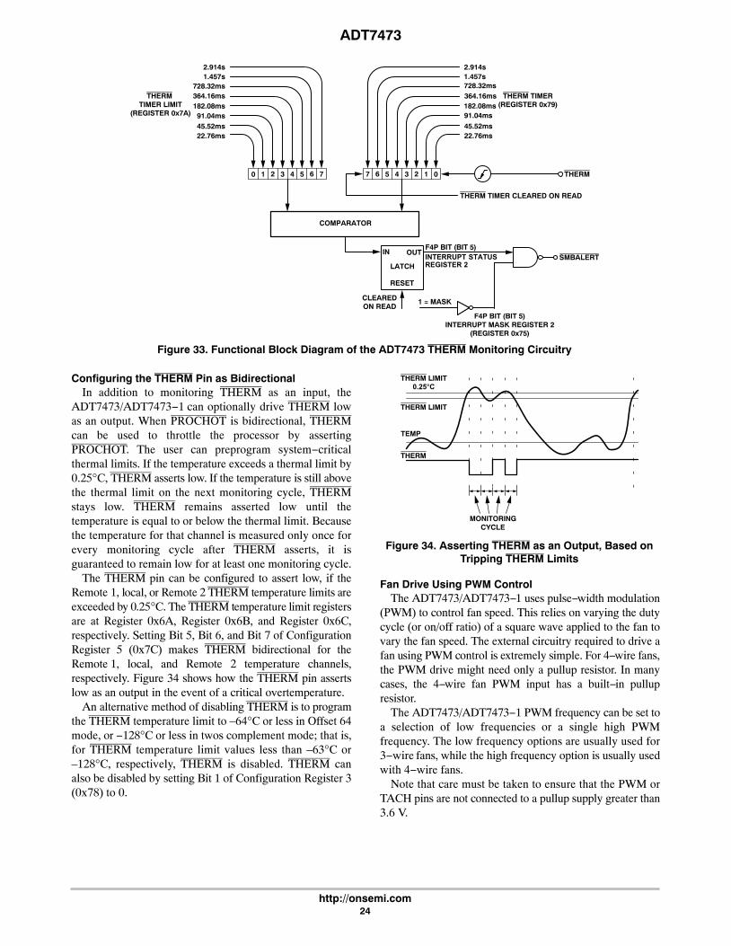
Figure 33. Functional Block Diagram of the ADT7473 THERM Monitoring Circuitry
22.76ms45.52ms91.04ms182.08ms364.16ms728.32ms1.457s2.914s
IN OUT
RESET
LATCH
CLEAREDON READ
F4P BIT (BIT 5)INTERRUPT MASK REGISTER 2
(REGISTER 0x75)
1 = MASK
F4P BIT (BIT 5)
COMPARATOR
22.76ms45.52ms91.04ms
182.08ms364.16ms728.32ms
1.457s2.914s
76543210 7 6 5 4 3 2 1 0
THERMTIMER LIMIT
(REGISTER 0x7A)
THERM TIMER(REGISTER 0x79)
THERM TIMER CLEARED ON READ
SMBALERT
THERM
INTERRUPT STATUSREGISTER 2
Configuring the THERM Pin as BidirectionalIn addition to monitoring THERM as an input, the
ADT7473/ADT7473−1 can optionally drive THERM lowas an output. When PROCHOT is bidirectional, THERMcan be used to throttle the processor by assertingPROCHOT. The user can preprogram system−criticalthermal limits. If the temperature exceeds a thermal limit by0.25°C, THERM asserts low. If the temperature is still abovethe thermal limit on the next monitoring cycle, THERMstays low. THERM remains asserted low until thetemperature is equal to or below the thermal limit. Becausethe temperature for that channel is measured only once forevery monitoring cycle after THERM asserts, it isguaranteed to remain low for at least one monitoring cycle.
The THERM pin can be configured to assert low, if theRemote 1, local, or Remote 2 THERM temperature limits areexceeded by 0.25°C. The THERM temperature limit registersare at Register 0x6A, Register 0x6B, and Register 0x6C,respectively. Setting Bit 5, Bit 6, and Bit 7 of ConfigurationRegister 5 (0x7C) makes THERM bidirectional for theRemote 1, local, and Remote 2 temperature channels,respectively. Figure 34 shows how the THERM pin assertslow as an output in the event of a critical overtemperature.
An alternative method of disabling THERM is to programthe THERM temperature limit to –64°C or less in Offset 64mode, or −128°C or less in twos complement mode; that is,for THERM temperature limit values less than –63°C or–128°C, respectively, THERM is disabled. THERM canalso be disabled by setting Bit 1 of Configuration Register 3(0x78) to 0.
Figure 34. Asserting THERM as an Output, Based onTripping THERM Limits
MONITORINGCYCLE
TEMP
THERM LIMIT0.25C
THERM LIMIT
THERM
Fan Drive Using PWM ControlThe ADT7473/ADT7473−1 uses pulse−width modulation
(PWM) to control fan speed. This relies on varying the dutycycle (or on/off ratio) of a square wave applied to the fan tovary the fan speed. The external circuitry required to drive afan using PWM control is extremely simple. For 4−wire fans,the PWM drive might need only a pullup resistor. In manycases, the 4−wire fan PWM input has a built−in pullupresistor.
The ADT7473/ADT7473−1 PWM frequency can be set toa selection of low frequencies or a single high PWMfrequency. The low frequency options are usually used for3−wire fans, while the high frequency option is usually usedwith 4−wire fans.
Note that care must be taken to ensure that the PWM orTACH pins are not connected to a pullup supply greater than3.6 V.

ADT7473
http://onsemi.com25
Many fans have internal pullups connected to theTACH/PWM pins to a supply greater than 3.6 V. Clampingor dividing down the voltage on these pins must be donewhere necessary. Clamping these pins with a Zener diodecan also help prevent back−EMF related noise from beingcoupled into the system.
For 3−wire fans, a single N−channel MOSFET is the onlydrive device required. The specifications of the MOSFETdepend on the maximum current required by the fan beingdriven. Typical notebook fans draw a nominal 170 mA;therefore, SOT devices can be used where board space is aconcern. In desktops, fans can typically draw 250 mA to300 mA each. If you drive several fans in parallel from asingle PWM output or drive larger server fans, the MOSFETmust handle the higher current requirements. The only otherstipulation is that the MOSFET have a gate voltage drive,VGS < 3.3 V, for direct interfacing to the PWM output. TheMOSFET should also have a low on resistance to ensure thatthere is not significant voltage drop across the FET, whichwould reduce the voltage applied across the fan and,therefore, the maximum operating speed of the fan.
Figure 35 shows how to drive a 3−wire fan using PWMcontrol.
Figure 35. Driving a 3−Wire Fan Using an N−ChannelMOSFET
ADT7473/ADT7473−1
TACH
PWM
12VFAN
Q1NDT3055L
3.3V
12V 12V
10kΩ
4.7kΩ
10kΩ
10kΩ
1N4148
Figure 35 uses a 10 k pullup resistor for the TACHsignal. This assumes that the TACH signal is anopen−collector from the fan. In all cases, the TACH signalfrom the fan must be kept below 3.6 V maximum to preventdamaging the ADT7473/ADT7473−1. If uncertain as towhether the fan used has an open−collector or totem poleTACH output, use one of the input signal conditioningcircuits shown in the Fan Speed Measurement section.
Figure 36 shows a fan drive circuit using an NPNtransistor such as a general−purpose MMBT2222. Whilethese devices are inexpensive, they tend to have much lowercurrent handling capabilities and higher on resistance thanMOSFETs. When choosing a transistor, care should be takento ensure that it meets the fan’s current requirements.
Ensure that the base resistor is chosen so that the transistoris saturated when the fan is powered on.
Figure 36. Driving a 3−Wire Fan Using an NPNTransistor
ADT7473/ADT7473−1
TACHTACH
PWM
12VFAN
Q1MMBT2222
3.3V
12V 12V
665Ω
4.7kΩ
10kΩ
10kΩ
1N4148
Because 4−wire fans are powered continuously, the fanspeed is not switched on or off as with previous PWMdriven/powered fans. This enables it to perform better than3−wire fans, especially for high frequency applications.
Figure 37 shows a typical drive circuit for 4−wire fans. Asthe PWM input on 4−wire fans is usually internally pulledup to a voltage greater than 3.6 V (the maximum voltageallowed on the ADT7473/ADT7473−1 PWM output), thePWM output should be clamped to 3.3 V using a Zenerdiode.
Figure 37. Driving a 4−Wire Fan
ADT7473/ADT7473−1
TACH
PWM
12V, 4−WIRE FAN
3.3V
12V 12V
4.7kΩ
10kΩ
10kΩVCC
TACHTACH
PWM
Driving Two Fans from PWM3The ADT7473/ADT7473−1 has four TACH inputs
available for fan speed measurement, but only three PWMdrive outputs. If a fourth fan is used in the system, it shouldbe driven from the PWM3 output in parallel with the thirdfan. Figure 38 shows how to drive two fans in parallel usinglow cost NPN transistors. Figure 39 shows the equivalentcircuit using a MOSFET.
Because the MOSFET can handle up to 3.5 A, it is simplya matter of connecting another fan directly in parallel withthe first. Care should be taken in designing drive circuitswith transistors and FETs to ensure the PWM pins are notrequired to source current and that they sink less than the8 mA maximum current specified on the data sheet.

ADT7473
http://onsemi.com26
Driving up to Three Fans from PWM3TACH measurements for fans are synchronized to
particular PWM channels; for example, TACH1 issynchronized to PWM1. TACH3 and TACH4 are bothsynchronized to PWM3, so PWM3 can drive two fans.Alternatively, PWM3 can be programmed to synchronizeTACH2, TACH3, and TACH4 to the PWM3 output. Thisallows PWM3 to drive two or three fans. In this case, thedrive circuitry looks the same, as shown in Figure 38 andFigure 39. The SYNC bit in Register 0x62 enables thisfunction.
Synchronization is not required in high frequency modewhen used with 4−wire fans.
Figure 38. Interfacing Two Fans in Parallel to thePWM3 Output UsingLow Cost NPN Transistors
ADT7473/ADT7473−1
PWM3
3.3V 3.3V
12V1N
4148
Q1MMBT3904
Q2MMBT2222
Q3MMBT2222
10k
10k
2.2k
1k
TACH3 TACH4
3.3V3.3V
Figure 39. Interfacing Two Fans in Parallel to thePWM3 Output Using a Single N−Channel MOSFET
ADT7473/ADT7473−1
PWM3
TACH3
TACH4
3.3V
3.3V
3.3V
+V +V
TACHTACH
Q1NDT3055L
1N4148
5V OR 12V FAN
5V OR 12V FAN
10kΩTYPICAL
10kΩTYPICAL
10kΩTYPICAL
3.3V
3.3V
Bit [4] (SYNC) of Enhanced Acoustics Register 1(0x62)
SYNC = 1, synchronizes TACH2, TACH3, and TACH4 toPWM3.
TACH InputsPin 4, Pin 6, Pin 7, and Pin 9 (when configured as TACH
inputs) are open−drain TACH inputs intended for fan speedmeasurement.
Signal conditioning in the ADT7473/ADT7473−1accommodates the slow rise and fall times typical of fantachometer outputs. The maximum input signal range is 0 Vto 3.6 V. In the event that these inputs are supplied from fanoutputs that exceed 0 V to 3.6 V, either resistive attenuation
of the fan signal or diode clamping must be included to keepinputs within an acceptable range.
Figure 40 to Figure 43 show circuits for most common fanTACH outputs.
If the fan TACH output has a resistive pullup to VCC, it canbe connected directly to the fan input, as shown in Figure 40.
Figure 40. Fan with TACH Pullup to VCC
12V
VCC
PULLUP4.7kΩ
TYPICAL
TACHOUTPUT
FAN SPEEDCOUNTER
TACHADT7473/ADT7473-1
If the fan output has a resistive pullup to 12 V (or othervoltage greater than 3.6 V), the fan output can be clampedwith a Zener diode, as shown in Figure 41. The Zener diodevoltage should be chosen so that it is greater than VIH of theTACH input, but less than 3.6 V, allowing for the voltagetolerance of the Zener. A value of between 3.0 V and 3.6 Vis suitable.
Figure 41. Fan with TACH Pullup to Voltage > 3.6 VClamped with Zener Diode
12V VCC
PULLUP4.7kΩ
TYPICALTACHOUTPUT
FAN SPEEDCOUNTER
TACH
ZD1*
*CHOOSE ZD1 VOLTAGE APPROXIMATELY 0.8 VCC
ADT7473/ADT7473-1
If the fan has a strong pullup (less than 1 k) to 12 V ora totem−pole output, a series resistor can be added to limitthe Zener current, as shown in Figure 42.
Figure 42. Fan with Strong TACH Pullup to > VCC orTotem−Pole Output, Clamped with Zener and Resistor
12V VCC
PULLUP4.7kΩ ORTYPICAL
TACHOUTPUT
FAN SPEEDCOUNTER
TACH
ZD1ZENER*
*CHOOSE ZD1 VOLTAGE APPROXIMATELY 0.8 VCC
ADT7473/ADT7473-1
Alternatively, a resistive attenuator can be used, as shownin Figure 43. R1 and R2 should be chosen such that
(eq. 3)2 V Vpullup R2Rpullup R1 R2 3.6 V
The fan inputs have an input resistance of nominally160 k to ground, which should be taken into account whencalculating resistor values.

ADT7473
http://onsemi.com27
With a pullup voltage of 12 V and pullup resistor less than1 k, suitable values for R1 and R2 are 120 k and 47 k,respectively. This gives a high input voltage of 3.35 V.
Figure 43. Fan with Strong TACH pullup to > VCC orTotem−Pole Output, Attenuated with R1/R2
12V VCC
<1kΩ
TACHOUTPUT
FAN SPEEDCOUNTER
TACH
R2*
*SEE TEXT
R1*
ADT7473/ADT7473-1
Fan Speed MeasurementThe fan counter does not count the fan TACH output
pulses directly, because the fan speed could be less than1000 RPM and it would take several seconds to accumulatea reasonably large and accurate count. Instead, the period ofthe fan revolution is measured by gating an on−chip 90 kHzoscillator into the input of a 16−bit counter for N periods ofthe fan TACH output (see Figure 44), so the accumulatedcount is actually proportional to the fan tachometer period,and inversely proportional to the fan speed.
N, the number of pulses counted, is determined by thesettings of the TACH pulses per revolution register (Register0x7B). This register contains two bits for each fan, allowingone, two (default), three, or four TACH pulses to be counted.
Figure 44. Fan Speed Measurement
1
2
3
4
CLOCK
PWM
TACH
Fan Speed Measurement RegistersThe fan tachometer readings are 16−bit values consisting
of a 2−byte read from the ADT7473/ADT7473−1.
Register 0x28, TACH1 Low Byte = 0x00 default
Register 0x29, TACH1 High Byte = 0x00 default
Register 0x2A, TACH2 Low Byte = 0x00 default
Register 0x2B, TACH2 High Byte = 0x00 default
Register 0x2C, TACH3 Low Byte = 0x00 default
Register 0x2D, TACH3 High Byte = 0x00 default
Register 0x2E, TACH4 Low Byte = 0x00 default
Register 0x2F, TACH4 High Byte = 0x00 default
Reading Fan Speed from the ADT7473/ADT7473−1The measurement of fan speeds involves a 2−register read
for each measurement. The low byte should be read first.This causes the high byte to be frozen until both high and lowbyte registers have been read, preventing erroneous TACHreadings. The fan tachometer reading registers report backthe number of 11.11 s period clocks (90 kHz oscillator)gated to the fan speed counter, from the rising edge of thefirst fan TACH pulse to the rising edge of the third fan TACHpulse (assuming two pulses per revolution are beingcounted). Because the device is essentially measuring thefan TACH period, the higher the count value, the slower thefan is actually running. A 16−bit fan tachometer reading of0xFFFF indicates either the fan has stalled or is running veryslowly (<100 RPM).
High Limit > Comparison PerformedBecause the actual fan TACH period is measured, falling
below a fan TACH limit by 1 sets the appropriate status bitand can be used to generate an SMBALERT.
Measuring Fan TACHWhen the ADT7473/ADT7473−1 starts up, TACH
measurements are locked. In effect, an internal read of thelow byte has been made for each TACH input. The net resultof this is that all TACH readings are locked until the highbyte is read from the corresponding TACH registers. AllTACH related interrupts are also ignored until theappropriate high byte is read.
Once the corresponding high byte has been read, TACHmeasurements are unlocked and interrupts are processed asnormal.
Fan TACH Limit RegistersThe fan TACH limit registers are 16−bit values consisting
of two bytes.
Register 0x54, TACH1 Minimum Low Byte = 0xFF default
Register 0x55, TACH1 Minimum High Byte = 0xFF default
Register 0x56, TACH2 Minimum Low Byte = 0xFF default
Register 0x57, TACH2 Minimum High Byte = 0xFF default
Register 0x58, TACH3 Minimum Low Byte = 0xFF default
Register 0x59, TACH3 Minimum High Byte = 0xFF default
Register 0x5A, TACH4 Minimum Low Byte = 0xFF default
Register 0x5B, TACH4 Minimum High Byte = 0xFF default
Fan Speed Measurement RateThe fan TACH readings are normally updated once every
second.The FAST bit (Bit 3) of Configuration Register 3 (0x78),
when set, updates the fan TACH readings every 250 ms.If any of the fans are not being driven by a PWM channel
but are powered directly from 5.0 V or 12 V, their associateddc bit in Configuration Register 3 should be set. This allowsTACH readings to be taken on a continuous basis for fans

ADT7473
http://onsemi.com28
connected directly to a dc source. For optimal results, theassociated dc bit should always be set when using 4−wirefans.
Calculating Fan SpeedAssuming a fan has two pulses per revolution (and two
pulses per revolution being measured), fan speed iscalculated by:
Fan Speed (RPM) = (90,000 x 60)/Fan TACH Readingwhere Fan TACH Reading is the 16−bit fan tachometer
reading.
Example
TACH1 High Byte (Register 0x29) = 0x17
TACH1 Low Byte (Register 0x28) = 0xFFWhat is Fan 1 speed in RPM?
Fan 1 TACH Reading = 0x17FF = 6143 (decimal)
RPM = (f x 60)/Fan 1 TACH Reading
RPM = (90000 x 60)/6143
Fan Speed = 879 RPM
Fan Pulses per RevolutionDifferent fan models can output either one, two, three, or
four TACH pulses per revolution. Once the number of fanTACH pulses has been determined, it can be programmedinto the fan pulses per revolution register (Register 0x7B)for each fan. Alternatively, this register can be used todetermine the number or pulses per revolution output by agiven fan. By plotting fan speed measurements at a 100%speed with different pulses per revolution setting, thesmoothest graph with the lowest ripple determines thecorrect pulses per revolution value.
TACH Pulses per Revolution Register
Bits [1:0] Fan 1 default = 2 pulses per revolution
Bits [3:2] Fan 2 default = 2 pulses per revolution
Bits [5:4] Fan 3 default = 2 pulses per revolution
Bits [7:6] Fan 4 default = 2 pulses per revolution00 = 1 pulse per revolution01 = 2 pulses per revolution10 = 3 pulses per revolution11 = 4 pulses per revolution
Fan Spin−UpThe ADT7473/ADT7473−1 has a unique fan spin−up
function. It spins the fan at 100% PWM duty cycle until twoTACH pulses are detected on the TACH input. Once twoTACH pulses are detected, the PWM duty cycle goes to theexpected running value, for example, 33%. The advantageis that fans have different spin−up characteristics and takedifferent times to overcome inertia. The ADT7473/ADT7473−1 runs the fans just fast enough to overcomeinertia and is quieter on spin−up than fans programmed fora given spin−up time.
Fan Startup TimeoutTo prevent the generation of false interrupts as a fan spins
up (because it is below running speed), the ADT7473/ADT7473−1 includes a fan startup timeout function. Duringthis time, the ADT7473/ADT7473−1 looks for two TACHpulses. If two TACH pulses are not detected, an interrupt isgenerated. Using Configuration Register 1 (0x40), Bit 5(FSPDIS), this functionality can be changed (see theDisabling Fan Startup Timeout section).
PWM1, PWM2, PWM3 Configuration Registers(Register 0x5C, Register 0x5D, and Register 0x5E)
Bits [2:0] SPIN, startup timeout for PWM1 = 0x5C,PWM2 = 0x5D, and PWM3 = 0x5E.
000 = No startup timeout001 = 100 ms010 = 250 ms default011 = 400 ms100 = 667 ms101 = 1 sec110 = 2 sec111 = 4 sec
Disabling Fan Startup TimeoutAlthough fan startup makes fan spin−ups much quieter
than fixed−time spin−ups, the option exists to use fixedspin−up times. Setting Bit 5 (FSPDIS) to 1 in ConfigurationRegister 1 (0x40) disables the spin−up for two TACH pulses.Instead, the fan spins up for the fixed time as selected inRegister 0x5C to Register 0x5E.
PWM Logic StateThe PWM outputs can be programmed high for a 100%
duty cycle (non−inverted) or low for a 100% duty cycle(inverted).
PWM1 Configuration Register (0x5C)
Bit 4 INV.0 = Logic high for a 100% PWM duty cycle1 = Logic low for a 100% PWM duty cycle
PWM2 Configuration Register (0x5D)
Bit 4 INV.0 = Logic high for a 100% PWM duty cycle1 = Logic low for a 100% PWM duty cycle
PWM3 Configuration Register (0x5E)
Bit 4 INV.0 = Logic high for a 100% PWM duty cycle1 = Logic low for a 100% PWM duty cycle
Low Frequency Mode PWM Drive FrequencyThe PWM drive frequency can be adjusted for the
application. Register 0x5F to Register 0x61 configure thePWM frequency for PWM1 to PWM3, respectively. In highfrequency mode, the PWM drive frequency is always22.5 kHz.
ADT7473
http://onsemi.com29
High Frequency Mode PWM DriveSetting Bit 3 of Register 0x5F, 60H or 61H enables high
frequency mode for fans 1, 2 and 3.
PWM Frequency Registers(Register 0x5F to Register 0x61)
Bits [2:0] FREQ000 = 11.0 Hz001 = 14.7 Hz010 = 22.1 Hz011 = 29.4 Hz100 = 35.3 Hz (default)101 = 44.1 Hz110 = 58.8 Hz111 = 88.2 Hz
Fan Speed ControlThe ADT7473/ADT7473−1 controls fan speed using
automatic and manual modes.In automatic fan speed control mode, fan speed is
automatically varied with temperature and without CPUintervention, once initial parameters are set up. Theadvantage of this is that, if the system hangs, the user isguaranteed the system is protected from overheating. Theautomatic fan speed control incorporates a feature calleddynamic TMIN calibration. This feature reduces the designeffort required to program the automatic fan speed controlloop. For more information and procedures on how toprogram the automatic fan speed control loop and dynamicTMIN calibration, see the Programming the Automatic FanSpeed Control Loop section.
In manual fan speed control mode, the ADT7473/ADT7473−1 allows the duty cycle of any PWM output to bemanually adjusted. This can be useful if the user wants tochange fan speed in software or adjust the PWM duty cycleoutput for test purposes. Bits [7:5] of Register 0x5C toRegister 0x5E (PWM configuration registers) control thebehavior of each PWM output.
PWM Configuration Registers(Register 0x5C to Register 0x5E)
Bits [7:5] BHVR111 = manual mode
Once under manual control, each PWM output can bemanually updated by writing to Register 0x30 to Register0x32 (PWM current duty cycle registers).
Programming the PWM Current Duty Cycle RegistersThe PWM current duty cycle registers are 8−bit registers
that allow the PWM duty cycle for each output to be setanywhere from 0% to 100% in steps of 0.39%.
The value to be programmed into the PWMMIN register isgiven by:
Value (decimal) = PWMMIN/0.39
Example 1
For a PWM duty cycle of 50%Value (decimal) = 50/0.39 = 128 (decimal)Value = 128 (decimal) or 0x80 (hex)
Example 2
For a PWM duty cycle of 33%Value (decimal) = 33/0.39 = 85 (decimal)Value = 85 (decimal) or 0x54 (hex)
PWM Current Duty Cycle Registers
Register 0x30, PWM1 Duty Cycle = 0x00 (0% default)
Register 0x31, PWM2 Duty Cycle = 0x00 (0% default)
Register 0x32, PWM3 Duty Cycle = 0x00 (0% default)
By reading the PWMx current duty cycle registers, theuser can keep track of the current duty cycle on each PWMoutput, even when the fans are running in automatic fanspeed control mode or acoustic enhancement mode. See theProgramming the Automatic Fan Speed Control Loopsection for details.
Fan Presence DetectThis feature can be used to determine if a 4−wire fan is
directly connected to a PWM output. This feature does notwork for 3−wire fans. To detect whether a 4−wire fan isconnected directly to a PWM output, the following stepsmust be performed in this order:
1. Drive the appropriate PWM outputs to 100% dutycycle.
2. Set Bit 0 of Configuration Register 2 (0x73).3. Wait 5 ms.4. Program the fans to run at a different speed if
necessary.5. Read the state of Bits [3:1] of Configuration
Register 2 (0x73). The state of these bits reflectswhether a 4−wire fan is directly connected to thePWM output.
As the detection time only takes 5 ms, programming thePWM outputs to 100% and then back to their normal speedis not noticeable in most cases.
Description of How Fan Presence Detect WorksTypical 4−wire fans have an internal pull up to 4.75 V
±10%, which typically sources 5 mA. While the detectioncycle is on, an internal current sink is turned on, sinkingcurrent from the fan’s internal pullup. By driving some of thecurrent from the fan’s internal pullup (~100 A), the logicbuffer switches to a defined logic state. If this state is high,a fan is present; if it is low, no fan is present.
The PWM input voltage should be clamped to 3.3 V. Thisensures the PWM output is not pulled to a voltage higherthan the maximum allowable voltage on that pin (3.6 V).

ADT7473
http://onsemi.com30
Sleep StatesThe ADT7473/ADT7473−1 has been specifically
designed to operate from a 3.3 V STBY supply. In computersthat support S3 and S5 states, the core voltage of theprocessor is lowered in these states. If using the dynamicTMIN mode, lowering the core voltage of the processorchanges the CPU temperature and the dynamics of thesystem under dynamic TMIN control. Likewise, whenmonitoring THERM, the THERM timer should be disabledduring these states.
Dynamic TMIN Control Register 1 (0X36) Bit [1]VCCPLO = 1
When the VCCP voltage drops below the VCCP low limit,the following occurs:
1. Status Bit 1 (VCCP) in Status Register 1 is set.2. SMBALERT is generated, if enabled.3. THERM monitoring is disabled. The THERM
timer should hold its value prior to the S3 or S5state.
4. Dynamic TMIN control is disabled. This preventsTMIN from being adjusted due to an S3 or S5 state.
5. The ADT7473/ADT7473−1 is prevented fromentering the shutdown state.
Once the core voltage, VCCP, goes above the VCCP lowlimit, everything is re−enabled, and the system resumesnormal operation.
XNOR Tree Test ModeThe ADT7473/ADT7473−1 includes an XNOR tree test
mode. This mode is useful for in−circuit test equipment atboard−level testing. By applying stimulus to the pinsincluded in the XNOR tree, it is possible to detect opens orshorts on the system board.
Figure 45 shows the signals that are exercised in theXNOR tree test mode. The XNOR tree test is invoked bysetting Bit 0 (XEN) of the XNOR tree test enable register(0x6F).
Figure 45. XNOR Tree Test
PWM1/XTOPWM3
PWM2
TACH4
TACH3
TACH2
TACH1
Power−On DefaultWhen the ADT7473 is powered up, it polls the VCCP
input. By default, the ADT7473−1 powers up with fansrunning, eliminating the need for polling of VCCP.
If VCCP stays below 0.75 V (the system CPU power railis not powered up), the ADT7473 assumes the functionality
of the default registers after the ADT74731 is addressed viaany valid SMBus transaction.
If VCC goes high (the system processor power rail ispowered up), a fail−safe timer begins to count down. If theADT7473 is not addressed by any valid SMBus transactionsbefore the fail−safe timeout (4.6 seconds) lapses, theADT7473 drives the fans to full speed. If the ADT7473 isaddressed by a valid SMBus transaction after this point, thefans stop, and the ADT7473 assumes its default settings andbegins normal operation.
If VCCP goes high (the system processor power rail ispowered up), then a fail−safe timer begins to count down. Ifthe ADT7473 is addressed by a valid SMBus transactionbefore the fail−safe timeout (4.6 seconds) lapses, then theADT7473 operates normally, assuming the functionality ofall the default registers. See the flow chart in Figure 46.
Figure 46. Power−On Flow Chart
ADT7473/ADT7473−1 IS POWERED UP
HAS THE ADT7473/ADT7473−1BEEN ACCESSED BY A VALID
SMBus TRANSACTION?
HAS THE ADT7473/ADT7473−1BEEN ACCESSED BY A VALID
SMBus TRANSACTION?
HAS THE ADT7473/ADT7473−1BEEN ACCESSED BY A VALID
SMBus TRANSACTION?
HAS THE ADT7473/ADT7473−1BEEN ACCESSED BY A VALID
SMBus TRANSACTION?
IS VCCP ABOVE 0.75V? CHECK VCCP
RUNS THE FANSTO FULL SPEED
SWITCH OFF FANS
START FAIL−SAFE TIMER
FAIL−SAFE TIMER ELAPSESAFTER THE FAIL−SAFE TIMEOUT
START UP THEADT7473/ADT7473−1 NORMALLY
Y
Y
Y
Y
N
N
N
N
N
Y
Programming the Automatic Fan Speed Control LoopTo understand the automatic fan speed control loop, it is
strongly recommended to use the ADT7473/ADT7473−1evaluation board and software while reading this section.
This section provides the system designer with anunderstanding of the automatic fan control loop, andprovides step−by−step guidance on effectively evaluatingand selecting critical system parameters. To optimize thesystem characteristics, the designer needs to consider thesystem configuration, including the number of fans, wherethey are located, and what temperatures are measured in theparticular system.

ADT7473
http://onsemi.com31
The mechanical or thermal engineer who is tasked withthe system thermal characterization should also be involvedat the beginning of the process.
Automatic Fan Control OverviewThe ADT7473/ADT7473−1 can automatically control the
speed of fans based on the measured temperature. This isdone independently of CPU intervention once initialparameters are set up.
The ADT7473/ADT7473−1 has a local temperaturesensor and two remote temperature channels that can beconnected to a CPU on−chip thermal diode (available onIntel Pentium class CPUs and other CPUs). These threetemperature channels can be used as the basis for automaticfan speed control to drive fans using PWM.
Automatic fan speed control reduces acoustic noise byoptimizing fan speed according to accurately measuredtemperature. Reducing fan speed can also decrease systemcurrent consumption. The automatic fan speed control modeis very flexible due to the number of programmableparameters, including TMIN and TRANGE. The TMIN andTRANGE values for a temperature channel and, therefore, fora given fan, are critical because they define the thermalcharacteristics of the system. The thermal validation of the
system is one of the most important steps in the designprocess, so these values should be selected carefully.
Figure 47 gives a top−level overview of the automatic fancontrol circuitry on the ADT7473/ADT7473−1. From asystems−level perspective, up to three system temperaturescan be monitored and used to control three PWM outputs.The three PWM outputs can be used to control up to fourfans. The ADT7473/ADT7473−1 allows the speed of fourfans to be monitored. Each temperature channel has athermal calibration block, allowing the designer toindividually configure the thermal characteristics of eachtemperature channel. For example, a designer can decide torun the CPU fan when CPU temperature increases above60°C, and a chassis fan when the local temperature increasesabove 45°C. At this stage, the designer has not assignedthese thermal calibration settings to a particular fan drive(PWM) channel. The right side of Figure 47 shows controlsthat are fan−specific. The designer has individual controlover parameters such as minimum PWM duty cycle, fanspeed failure thresholds, and even ramp control of the PWMoutputs. Automatic fan control, then, ultimately allowsgraceful fan speed changes that are less perceptible to thesystem user.
Figure 47. Automatic Fan Control Block Diagram
MUX
THERMAL CALIBRATION
0%TMIN TRANGE
THERMAL CALIBRATION100%
0%TMIN TRANGE
THERMAL CALIBRATION100%
0%TMIN TRANGEREMOTE 1
TEMP
LOCALTEMP
REMOTE 2TEMP
TACHOMETER 1MEASUREMENT
PWMCONFIG
PWMMIN
PWM1
RAMPCONTROL
(ACOUSTICENHANCEMENT)
PWMGENERATOR
TACHOMETER 2MEASUREMENT
PWMCONFIG
PWMMIN
PWM2
RAMPCONTROL
(ACOUSTICENHANCEMENT)
PWMGENERATOR
TACHOMETER 3AND 4
MEASUREMENT
PWMCONFIG
PWMMIN
PWM3
RAMPCONTROL
(ACOUSTICENHANCEMENT)
PWMGENERATOR
100%
TACH1
TACH2
TACH3

ADT7473
http://onsemi.com32
Step 1: Hardware ConfigurationDuring system design, the motherboard sensing and
control capabilities should be addressed early in the designstages. Decisions about how these capabilities are usedshould involve the system thermal/mechanical engineer.Consider the following questions:
1. What ADT7473/ADT7473−1 functionality will beused?• PWM2 or SMBALERT for ADT7473?
• THERM_LATCH or PWM2 for ADT7473−1?
• TACH4 fan speed measurement or over−temperature THERM function? The ADT7473/ADT7473−1 offers multifunctional pins that canbe reconfigured to suit different systemrequirements and physical layouts. Thesemultifunction pins are software programmable.
2. How many fans will be supported in the system,three or four? This influences the choice ofwhether to use the TACH4 pin or to reconfigure itfor the THERM function.
3. Is the CPU fan to be controlled using theADT7473/ADT7473−1 or will it run at full speed100% of the time?If run at full speed, 100% of the time, this frees upa PWM output, but the system is louder.
4. Where will the ADT7473/ADT7473−1 bephysically located in the system?
This influences the assignment of the temperaturemeasurement channels to particular system thermal zones.For example, locating the ADT7473/ADT7473−1 close tothe VRM controller circuitry allows the VRM temperatureto be monitored using the local temperature channel.
Figure 48. Hardware Configuration Example

ADT7473
http://onsemi.com33
Recommended Implementation 1Configuring the ADT7473, as in Figure 49 provides the
system designer with the following features:• Two PWM outputs for fan control of up to three fans.
(The front and rear chassis fans are connected inparallel.)
• Three TACH fan speed measurement inputs.
• VCC measured internally through Pin 4.
• CPU core voltage measurement (VCORE).
• VRM temperature using local temperature sensor.
• CPU temperature measured using the Remote 1temperature channel.
• Ambient temperature measured through the Remote 2temperature channel.
• Bidirectional THERM pin allows the monitoring ofPROCHOT output from an Intel Pentium 4 processor,for example, or can be used as an overtemperatureTHERM output.
• SMBALERT system interrupt output.
Figure 49. Recommended Implementation 1
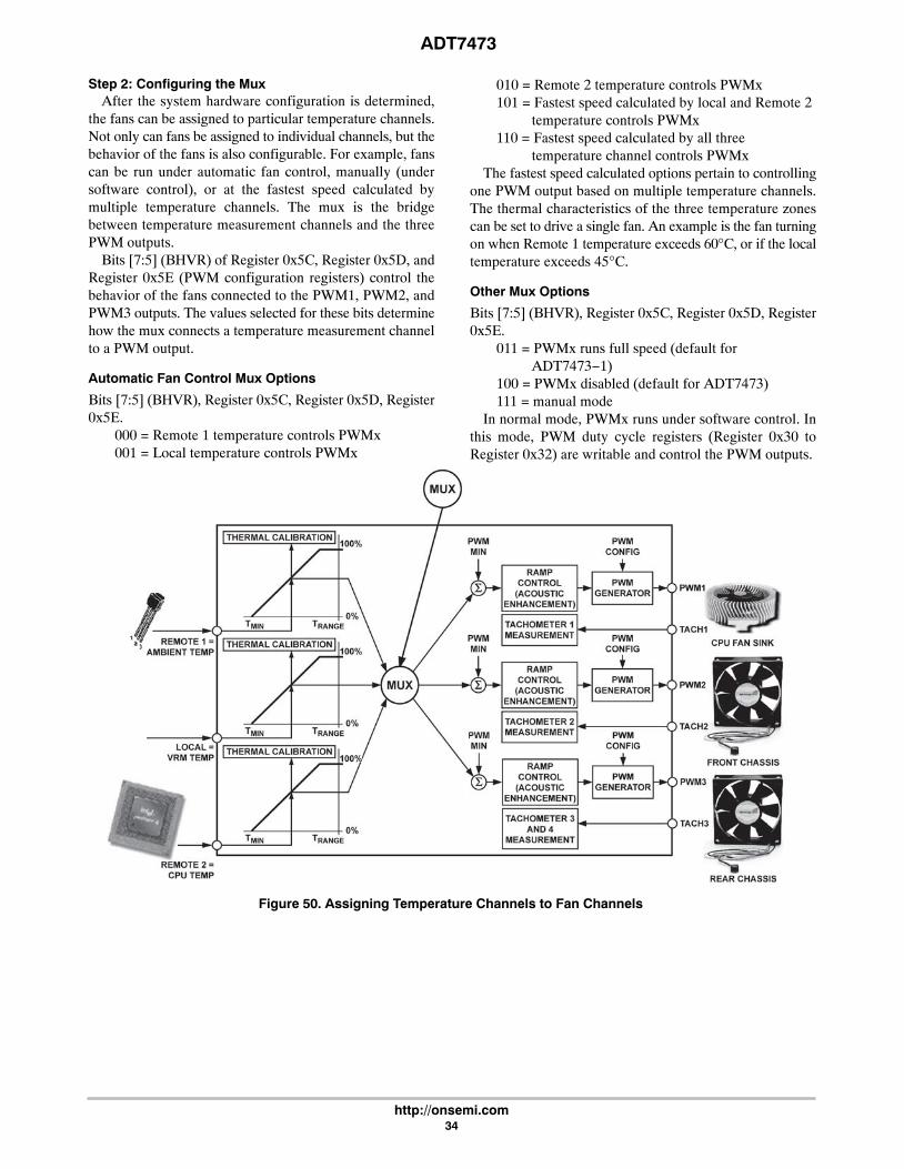
ADT7473
http://onsemi.com34
Step 2: Configuring the MuxAfter the system hardware configuration is determined,
the fans can be assigned to particular temperature channels.Not only can fans be assigned to individual channels, but thebehavior of the fans is also configurable. For example, fanscan be run under automatic fan control, manually (undersoftware control), or at the fastest speed calculated bymultiple temperature channels. The mux is the bridgebetween temperature measurement channels and the threePWM outputs.
Bits [7:5] (BHVR) of Register 0x5C, Register 0x5D, andRegister 0x5E (PWM configuration registers) control thebehavior of the fans connected to the PWM1, PWM2, andPWM3 outputs. The values selected for these bits determinehow the mux connects a temperature measurement channelto a PWM output.
Automatic Fan Control Mux Options
Bits [7:5] (BHVR), Register 0x5C, Register 0x5D, Register0x5E.
000 = Remote 1 temperature controls PWMx001 = Local temperature controls PWMx
010 = Remote 2 temperature controls PWMx101 = Fastest speed calculated by local and Remote 2
temperature controls PWMx110 = Fastest speed calculated by all three
temperature channel controls PWMxThe fastest speed calculated options pertain to controlling
one PWM output based on multiple temperature channels.The thermal characteristics of the three temperature zonescan be set to drive a single fan. An example is the fan turningon when Remote 1 temperature exceeds 60°C, or if the localtemperature exceeds 45°C.
Other Mux Options
Bits [7:5] (BHVR), Register 0x5C, Register 0x5D, Register0x5E.
011 = PWMx runs full speed (default forADT7473−1)
100 = PWMx disabled (default for ADT7473)111 = manual mode
In normal mode, PWMx runs under software control. Inthis mode, PWM duty cycle registers (Register 0x30 toRegister 0x32) are writable and control the PWM outputs.
Figure 50. Assigning Temperature Channels to Fan Channels
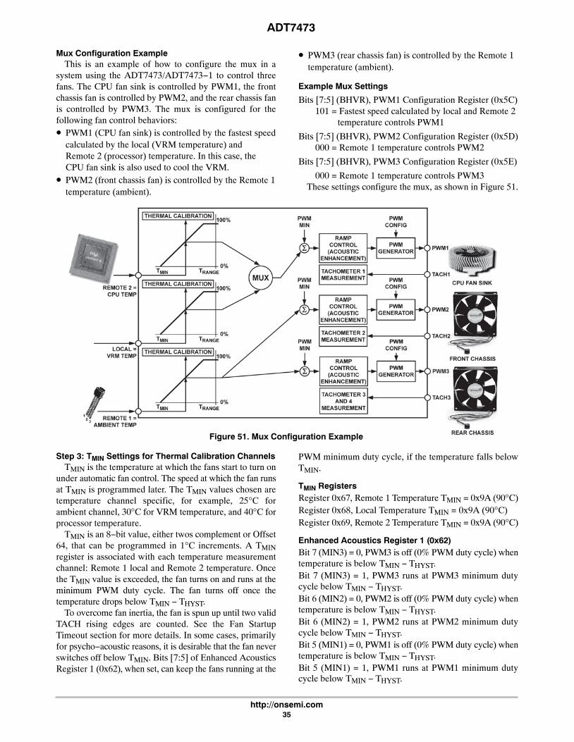
ADT7473
http://onsemi.com35
Mux Configuration ExampleThis is an example of how to configure the mux in a
system using the ADT7473/ADT7473−1 to control threefans. The CPU fan sink is controlled by PWM1, the frontchassis fan is controlled by PWM2, and the rear chassis fanis controlled by PWM3. The mux is configured for thefollowing fan control behaviors:• PWM1 (CPU fan sink) is controlled by the fastest speed
calculated by the local (VRM temperature) andRemote 2 (processor) temperature. In this case, theCPU fan sink is also used to cool the VRM.
• PWM2 (front chassis fan) is controlled by the Remote 1temperature (ambient).
• PWM3 (rear chassis fan) is controlled by the Remote 1temperature (ambient).
Example Mux Settings
Bits [7:5] (BHVR), PWM1 Configuration Register (0x5C)101 = Fastest speed calculated by local and Remote 2
temperature controls PWM1
Bits [7:5] (BHVR), PWM2 Configuration Register (0x5D)000 = Remote 1 temperature controls PWM2
Bits [7:5] (BHVR), PWM3 Configuration Register (0x5E)
000 = Remote 1 temperature controls PWM3These settings configure the mux, as shown in Figure 51.
Figure 51. Mux Configuration Example
Step 3: TMIN Settings for Thermal Calibration ChannelsTMIN is the temperature at which the fans start to turn on
under automatic fan control. The speed at which the fan runsat TMIN is programmed later. The TMIN values chosen aretemperature channel specific, for example, 25°C forambient channel, 30°C for VRM temperature, and 40°C forprocessor temperature.
TMIN is an 8−bit value, either twos complement or Offset64, that can be programmed in 1°C increments. A TMINregister is associated with each temperature measurementchannel: Remote 1 local and Remote 2 temperature. Oncethe TMIN value is exceeded, the fan turns on and runs at theminimum PWM duty cycle. The fan turns off once thetemperature drops below TMIN − THYST.
To overcome fan inertia, the fan is spun up until two validTACH rising edges are counted. See the Fan StartupTimeout section for more details. In some cases, primarilyfor psycho−acoustic reasons, it is desirable that the fan neverswitches off below TMIN. Bits [7:5] of Enhanced AcousticsRegister 1 (0x62), when set, can keep the fans running at the
PWM minimum duty cycle, if the temperature falls belowTMIN.
TMIN RegistersRegister 0x67, Remote 1 Temperature TMIN = 0x9A (90°C)Register 0x68, Local Temperature TMIN = 0x9A (90°C)Register 0x69, Remote 2 Temperature TMIN = 0x9A (90°C)
Enhanced Acoustics Register 1 (0x62)Bit 7 (MIN3) = 0, PWM3 is off (0% PWM duty cycle) whentemperature is below TMIN − THYST.Bit 7 (MIN3) = 1, PWM3 runs at PWM3 minimum dutycycle below TMIN − THYST.Bit 6 (MIN2) = 0, PWM2 is off (0% PWM duty cycle) whentemperature is below TMIN − THYST.Bit 6 (MIN2) = 1, PWM2 runs at PWM2 minimum dutycycle below TMIN − THYST.Bit 5 (MIN1) = 0, PWM1 is off (0% PWM duty cycle) whentemperature is below TMIN − THYST.Bit 5 (MIN1) = 1, PWM1 runs at PWM1 minimum dutycycle below TMIN − THYST.
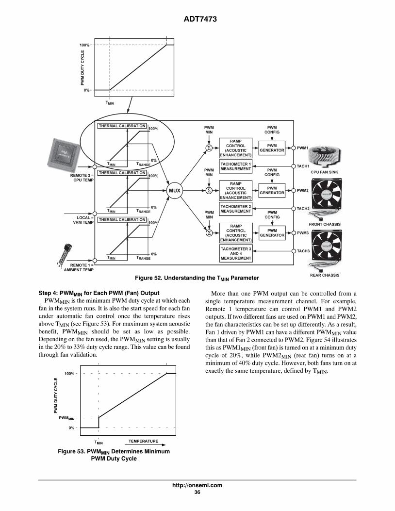
ADT7473
http://onsemi.com36
Figure 52. Understanding the TMIN Parameter
Step 4: PWMMIN for Each PWM (Fan) OutputPWMMIN is the minimum PWM duty cycle at which each
fan in the system runs. It is also the start speed for each fanunder automatic fan control once the temperature risesabove TMIN (see Figure 53). For maximum system acousticbenefit, PWMMIN should be set as low as possible.Depending on the fan used, the PWMMIN setting is usuallyin the 20% to 33% duty cycle range. This value can be foundthrough fan validation.
Figure 53. PWMMIN Determines MinimumPWM Duty Cycle
TEMPERATURETMIN
100%
PWMMIN
0%
PW
M D
UT
Y C
YC
LE
More than one PWM output can be controlled from asingle temperature measurement channel. For example,Remote 1 temperature can control PWM1 and PWM2outputs. If two different fans are used on PWM1 and PWM2,the fan characteristics can be set up differently. As a result,Fan 1 driven by PWM1 can have a different PWMMIN valuethan that of Fan 2 connected to PWM2. Figure 54 illustratesthis as PWM1MIN (front fan) is turned on at a minimum dutycycle of 20%, while PWM2MIN (rear fan) turns on at aminimum of 40% duty cycle. However, both fans turn on atexactly the same temperature, defined by TMIN.

ADT7473
http://onsemi.com37
Figure 54. Operating Two Different Fans from aSingle Temperature Channel
TEMPERATURETMIN
100%
PWM1MIN
0%
PW
M D
UT
Y C
YC
LE
PWM1
PWM2
PWM2MIN
Programming the PWMMIN RegistersThe PWMMIN registers are 8−bit registers that allow the
minimum PWM duty cycle for each output to be configuredanywhere from 0% to 100%. This allows the minimumPWM duty cycle to be set in steps of 0.39%.
The value to be programmed into the PWMMIN register isgiven by:
Value (decimal) = PWMMIN/0.39
Example 1
For a minimum PWM duty cycle of 50%Value (decimal) = 50/0.39 = 128 (decimal)Value = 128 (decimal) or 80 (hex)
Example 2
For a minimum PWM duty cycle of 33%Value (decimal) = 33/0.39 = 85 (decimal)Value = 85 (decimal) or 54 (hex)
PWMMIN Registers
Register 0x64, PWM1 Minimum Duty Cycle = 0x80 (50%default)
Register 0x65, PWM2 Minimum Duty Cycle = 0x80 (50%default)
Register 0x66, PWM3 Minimum Duty Cycle = 0x80 (50%default)
Note on Fan Speed and PWM Duty CycleThe PWM duty cycle does not directly correlate to fan
speed in RPM. Running a fan at 33% PWM duty cycle doesnot equate to running the fan at 33% speed. Driving a fan at33% PWM duty cycle actually runs the fan at closer to 50%of its full speed. This is because fan speed in %RPMgenerally relates to the square root of PWM duty cycle.Given a PWM square wave as the drive signal, fan speed inRPM approximates to:
% fanspeed PWM duty cycle 10 (eq. 4)
Step 5: PWMMAX for PWM (Fan) OutputsPWMMAX is the maximum duty cycle at which each fan
in the system runs under the automatic fan speed controlloop. For maximum system acoustic benefit, PWMMAXshould be as low as possible, but should be capable ofmaintaining the processor temperature limit at an acceptablelevel. If the THERM temperature limit is exceeded, the fansare still boosted to 100% for fail−safe cooling (seeFigure 55).
There is a PWMMAX limit for each fan channel. Thedefault value of this register is 0xFF and thus has no effectunless it is programmed.
Figure 55. PWMMAX Determines Maximum PWM DutyCycle Below the THERM Temperature Limit
TEMPERATURETMIN
100%
PWMMIN
0%
PW
M D
UT
Y C
YC
LE PWMMAX
Programming the PWMMAX RegistersThe PWMMAX registers are 8−bit registers that allow the
maximum PWM duty cycle for each output to be configuredanywhere from 0% to 100%. This allows the maximumPWM duty cycle to be set in steps of 0.39%.
The value to be programmed into the PWMMAX registeris given by:
Value (decimal) = PWMMAX/0.39
Example 1
For a maximum PWM duty cycle of 50%Value (decimal) = 50/0.39 = 128 (decimal)Value = 128 (decimal) or 80 (hex)
Example 2
For a minimum PWM duty cycle of 75%Value (decimal) = 75/0.39 = 85 (decimal)Value = 192 (decimal) or C0 (hex)
PWMMAX Registers
Register 0x38, PWM1 Maximum Duty Cycle = 0xFF(100% default)
Register 0x39, PWM2 Maximum Duty Cycle = 0xFF(100% default)
Register 0x3A, PWM3 Maximum Duty Cycle = 0xFF(100% default)
See the Note on Fan Speed and PWM Duty Cycle section.
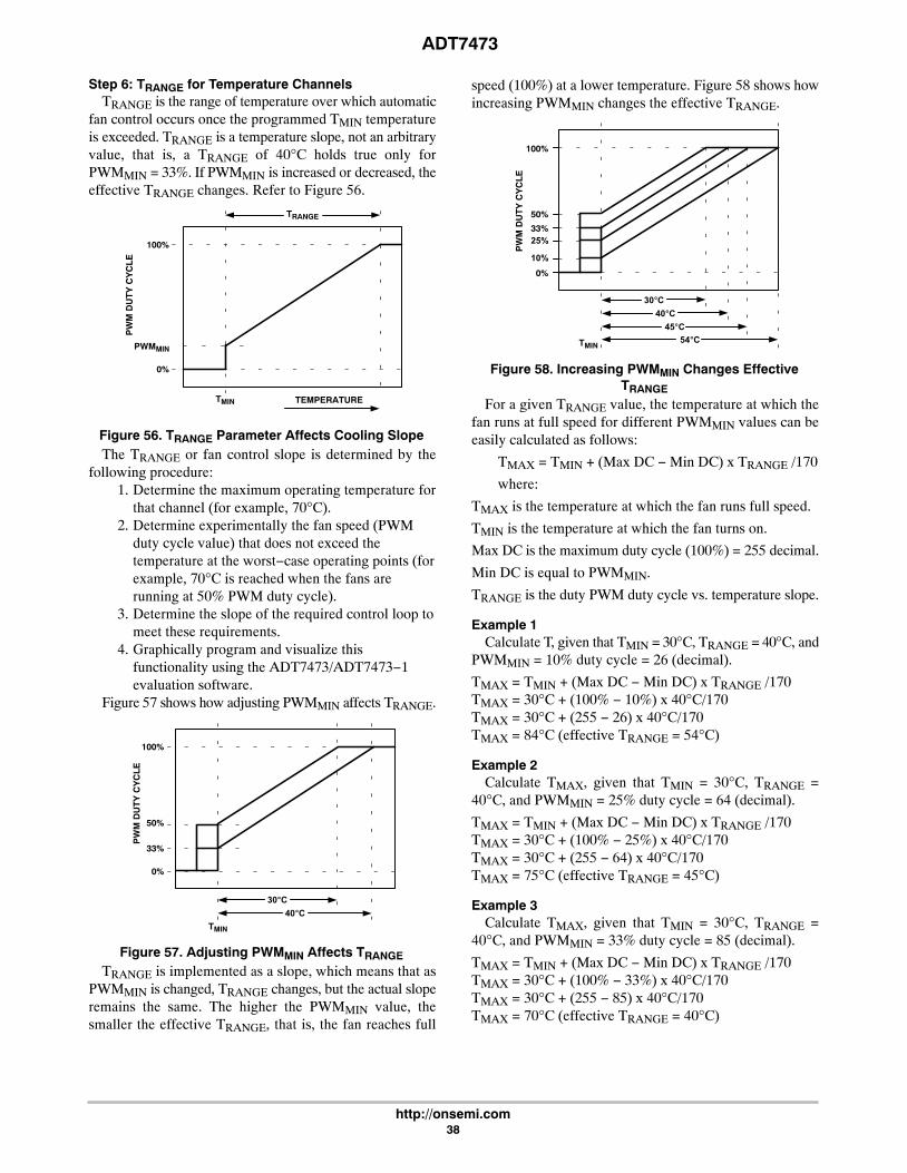
ADT7473
http://onsemi.com38
Step 6: TRANGE for Temperature ChannelsTRANGE is the range of temperature over which automatic
fan control occurs once the programmed TMIN temperatureis exceeded. TRANGE is a temperature slope, not an arbitraryvalue, that is, a TRANGE of 40°C holds true only forPWMMIN = 33%. If PWMMIN is increased or decreased, theeffective TRANGE changes. Refer to Figure 56.
Figure 56. TRANGE Parameter Affects Cooling Slope
TEMPERATURETMIN
100%
PWMMIN
0%
PW
M D
UT
Y C
YC
LE
TRANGE
The TRANGE or fan control slope is determined by thefollowing procedure:
1. Determine the maximum operating temperature forthat channel (for example, 70°C).
2. Determine experimentally the fan speed (PWMduty cycle value) that does not exceed thetemperature at the worst−case operating points (forexample, 70°C is reached when the fans arerunning at 50% PWM duty cycle).
3. Determine the slope of the required control loop tomeet these requirements.
4. Graphically program and visualize thisfunctionality using the ADT7473/ADT7473−1evaluation software.
Figure 57 shows how adjusting PWMMIN affects TRANGE.
Figure 57. Adjusting PWMMIN Affects TRANGE
TMIN
100%
33%
0%
PW
M D
UT
Y C
YC
LE
50%
30C
40C
TRANGE is implemented as a slope, which means that asPWMMIN is changed, TRANGE changes, but the actual sloperemains the same. The higher the PWMMIN value, thesmaller the effective TRANGE, that is, the fan reaches full
speed (100%) at a lower temperature. Figure 58 shows howincreasing PWMMIN changes the effective TRANGE.
Figure 58. Increasing PWMMIN Changes EffectiveTRANGE
TMIN
100%
33%
0%
PW
M D
UT
Y C
YC
LE
50%
30C
40C
25%
10%
45C
54C
For a given TRANGE value, the temperature at which thefan runs at full speed for different PWMMIN values can beeasily calculated as follows:
TMAX = TMIN + (Max DC − Min DC) x TRANGE /170
where:
TMAX is the temperature at which the fan runs full speed.
TMIN is the temperature at which the fan turns on.
Max DC is the maximum duty cycle (100%) = 255 decimal.
Min DC is equal to PWMMIN.
TRANGE is the duty PWM duty cycle vs. temperature slope.
Example 1Calculate T, given that TMIN = 30°C, TRANGE = 40°C, and
PWMMIN = 10% duty cycle = 26 (decimal).
TMAX = TMIN + (Max DC − Min DC) x TRANGE /170TMAX = 30°C + (100% − 10%) x 40°C/170TMAX = 30°C + (255 − 26) x 40°C/170TMAX = 84°C (effective TRANGE = 54°C)
Example 2Calculate TMAX, given that TMIN = 30°C, TRANGE =
40°C, and PWMMIN = 25% duty cycle = 64 (decimal).
TMAX = TMIN + (Max DC − Min DC) x TRANGE /170TMAX = 30°C + (100% − 25%) x 40°C/170TMAX = 30°C + (255 − 64) x 40°C/170TMAX = 75°C (effective TRANGE = 45°C)
Example 3Calculate TMAX, given that TMIN = 30°C, TRANGE =
40°C, and PWMMIN = 33% duty cycle = 85 (decimal).
TMAX = TMIN + (Max DC − Min DC) x TRANGE /170TMAX = 30°C + (100% − 33%) x 40°C/170TMAX = 30°C + (255 − 85) x 40°C/170TMAX = 70°C (effective TRANGE = 40°C)

ADT7473
http://onsemi.com39
Example 4Calculate TMAX, given that TMIN = 30°C, TRANGE =
40°C, and PWMMIN = 50% duty cycle = 128 (decimal).
TMAX = TMIN + (Max DC − Min DC) x TRANGE /170TMAX = 30°C + (100% − 50%) x 40°C/170TMAX = 30°C + (255 − 128) x 40°C/170TMAX = 60°C (effective TRANGE = 30°C)
Selecting a TRANGE SlopeThe TRANGE value can be selected for each temperature
channel: Remote 1, local, and Remote 2. Bits [7:4](TRANGE) of Register 0x5F to Register 0x61 define theTRANGE value for each temperature channel.
Table 13. Selecting a TRANGE Value
Bits [7:4] (Note 1) TRANGE (C)
0000 2
0001 2.5
0010 3.33
0011 4
0100 5
0101 6.67
0110 8
0111 10
1000 13.33
1001 16
1010 20
1011 26.67
1100 32 (default)
1101 40
1110 53.33
1111 80
1. Register 0x5F configures Remote 1 TRANGE; Register 0x60configures local TRANGE; Register 0x61 configures Remote 2TRANGE.
Summary of TRANGE FunctionWhen using the automatic fan control function, the
temperature at which the fan reaches full speed can becalculated by:
(eq. 5)TMAX TMIN TTRANGE
Equation 1 holds true only when PWMMIN is equal to 33%PWM duty cycle.
Increasing or decreasing PWMMIN changes the effectiveTRANGE, although the fan control still follows the samePWM duty cycle to temperature slope. The effectiveTRANGE for different PWMMIN values can be calculatedusing Equation 6.
(eq. 6)
TMAX TMIN Max DC Min DC TTRANGE170
where (Max DC − Min DC) x TRANGE/170 is the effectiveTRANGE value.
See the Note on Fan Speed and PWM Duty Cycle section.Figure 59 shows PWM duty cycle vs. temperature for eachTRANGE setting. The lower graph shows how each TRANGEsetting affects fan speed vs. temperature. As indicated by thegraph, the effect on fan speed is nonlinear.
The graphs in Figure 59 assume the fan starts from 0%PWM duty cycle. Clearly, the minimum PWM duty cycle,PWMMIN, needs to be factored in to see how the loopactually performs in the system. Figure 60 shows howTRANGE is affected when the PWMMIN value is set to 20%.It can be seen that the fan actually runs at about 45% fanspeed when the temperature exceeds TMIN.
Figure 59. TRANGE vs. Actual Fan Speed Profile
TEMPERATURE ABOVE TMIN
0 20 40 60 80 100 1200
FA
N S
PE
ED
(%
OF
MA
X)
10
20
30
40
50
60
70
80
90
100
TEMPERATURE ABOVE TMIN
0 20 40 60 80 100 1200
PW
M D
UT
Y C
YC
LE
(%
)
10
20
30
40
50
60
70
80
90
100
2C
80C
53.3C
40C
32C
26.6C
20C
16C
13.3C
10C
8C
6.67C
5C
4C
3.33C
2.5C
2C
80C
53.3C
40C
32C
26.6C
20C
16C
13.3C
10C
8C
6.67C
5C
4C
3.33C
2.5C

ADT7473
http://onsemi.com40
Figure 60. TRANGE and % Fan Speed Slopes withPWMMIN = 20%
TEMPERATURE ABOVE TMIN
0 20 40 60 80 100 1200
PW
M D
UT
Y C
YC
LE
(%
)
10
20
30
40
50
60
70
80
90
100
TEMPERATURE ABOVE TMIN
0 20 40 60 80 100 1200
FA
N S
PE
ED
(%
OF
MA
X)
10
20
30
40
50
60
70
80
90
100
2C
80C
53.3C
40C
32C
26.6C
20C
16C
13.3C
10C
8C
6.67C
5C
4C
3.33C
2.5C
2C
80C
53.3C
40C
32C
26.6C
20C
16C
13.3C
10C
8C
6.67C
5C
4C
3.33C
2.5C
Example: Determining TRANGE for Each TemperatureChannel
The following example shows how the different TMIN andTRANGE settings can be applied to three different thermalzones. In this example, the following TRANGE values apply:
TRANGE = 80°C for ambient temperatureTRANGE = 53.3°C for CPU temperatureTRANGE = 40°C for VRM temperature
This example uses the mux configuration described in theStep 2: Configuring the Mux section, with the ADT7473/ADT7473−1 connected as shown in Figure 61. Both CPUtemperature and VRM temperature drive the CPU fanconnected to PWM1.
Ambient temperature drives the front chassis fan and rearchassis fan connected to PWM2 and PWM3. The frontchassis fan is configured to run at PWMMIN = 20%. The rearchassis fan is configured to run at PWMMIN = 30%. TheCPU fan is configured to run at PWMMIN = 10%.
Note on 4−Wire FansThe control range for 4−wire fans is much wider than that
for 3−wire fans. In many cases, 4−wire fans can start with aPWM drive of as little as 20%.
TEMPERATURE ABOVE TMIN
0 10 20 30 40 10050 60 70 80 900
PW
M D
UT
Y C
YC
LE
(%
)
10
20
30
40
50
60
70
80
90
100
TEMPERATURE ABOVE TMIN
0
FA
N S
PE
ED
(%
MA
X R
PM
)
10
20
30
40
50
60
70
80
90
100
0 10 20 30 40 10050 60 70 80 90
Figure 61. TRANGE and % Fan Speed Slopes for VRM,Ambient, and CPU Temperature Channels
Step 7: TTHERM for Temperature ChannelsTTHERM is the absolute maximum temperature allowed
on a temperature channel. When operating above thistemperature, a component such as the CPU or VRM mightbe beyond its safe operating limit. When the temperaturemeasured exceeds TTHERM all fans are driven at 100%PWM duty cycle (full speed) to provide critical systemcooling.
The fans remain running at 100% until the temperaturedrops below TTHERM − hysteresis, where hysteresis is thenumber programmed into the hysteresis registers (Register0x6D and Register 0x6E). The default hysteresis value is 4°C.
The TTHERM limit should be considered the maximumworst−case operating temperature of the system. Becauseexceeding any TTHERM limit runs all fans at 100%, it hasvery negative acoustic effects. Ultimately, this limit shouldbe set up as a fail−safe, and it should not be exceeded undernormal system operating conditions.
Note that the TTHERM limits are nonmaskable and affectthe fan speed no matter how the automatic fan controlsettings are configured. This allows some flexibility becausea TRANGE value can be selected based on its slope, while ahard limit (such as 70°C), can be programmed as TMAX (the

ADT7473
http://onsemi.com41
temperature at which the fan reaches full speed) by settingTTHERM to that limit (for example, 70°C).
THERM Registers
Register 0x6A, Remote 1 THERM Temperature Limit =0xA4 (100°C default)
Register 0x6B, Local THERM Temperature Limit = 0xA4(100°C default)
Register 0x6C, Remote 2 THERM Temperature Limit =0xA4 (100°C default)
Hysteresis Registers
Register 0x6D, Remote 1 Local Temperature HysteresisRegister
Bits [7:4] Remote 1 temperature hysteresis (4°C default)
Bits [3:0] Local temperature hysteresis (4°C default)
Register 0x6E, Remote 2 Temperature Hysteresis Register
Bits [7:4] Remote 2 temperature hysteresis (4°C default)
Because each hysteresis setting is four bits, hysteresisvalues are programmable from 1°C to 15°C. It is notrecommended that hysteresis values be programmed to 0°C,because this disables hysteresis. In effect, this would causethe fans to cycle between normal speed and 100% speed,creating unsettling acoustic noise.
Figure 62. How TTHERMRelates to Automatic Fan Control
Step 8: THYST for Temperature ChannelsTHYST is the amount of extra cooling a fan provides after
the temperature measured has dropped back below TMINbefore the fan turns off. The premise for temperaturehysteresis (THYST) is that, without it, the fan would merelychatter or cycle on and off regularly whenever temperatureis hovering at about the TMIN setting.
The THYST value chosen determines the amount of timeneeded for the system to cool down or heat up as the fan turnson and off. Values of hysteresis are programmable in therange 1°C to 15°C. Larger values of THYST prevent the fansfrom chattering on and off. The THYST default value is setat 4°C.
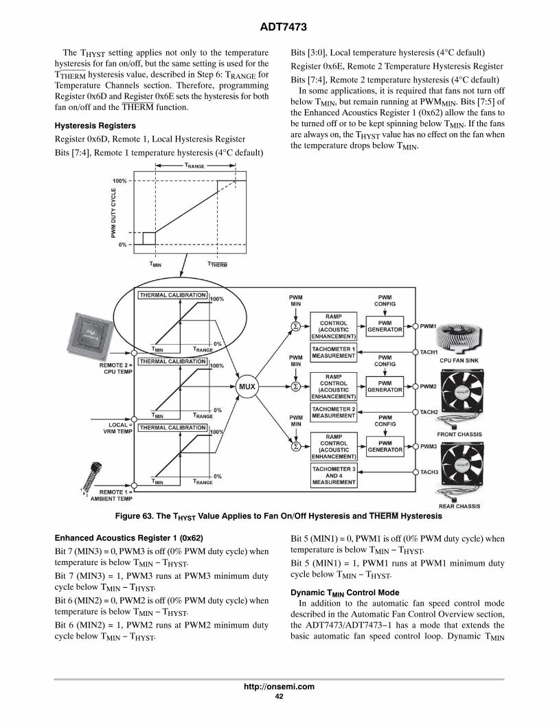
ADT7473
http://onsemi.com42
The THYST setting applies not only to the temperaturehysteresis for fan on/off, but the same setting is used for theTTHERM hysteresis value, described in Step 6: TRANGE forTemperature Channels section. Therefore, programmingRegister 0x6D and Register 0x6E sets the hysteresis for bothfan on/off and the THERM function.
Hysteresis Registers
Register 0x6D, Remote 1, Local Hysteresis Register
Bits [7:4], Remote 1 temperature hysteresis (4°C default)
Bits [3:0], Local temperature hysteresis (4°C default)
Register 0x6E, Remote 2 Temperature Hysteresis Register
Bits [7:4], Remote 2 temperature hysteresis (4°C default)In some applications, it is required that fans not turn off
below TMIN, but remain running at PWMMIN. Bits [7:5] ofthe Enhanced Acoustics Register 1 (0x62) allow the fans tobe turned off or to be kept spinning below TMIN. If the fansare always on, the THYST value has no effect on the fan whenthe temperature drops below TMIN.
Figure 63. The THYST Value Applies to Fan On/Off Hysteresis and THERM Hysteresis
Enhanced Acoustics Register 1 (0x62)
Bit 7 (MIN3) = 0, PWM3 is off (0% PWM duty cycle) whentemperature is below TMIN − THYST.
Bit 7 (MIN3) = 1, PWM3 runs at PWM3 minimum dutycycle below TMIN − THYST.
Bit 6 (MIN2) = 0, PWM2 is off (0% PWM duty cycle) whentemperature is below TMIN − THYST.
Bit 6 (MIN2) = 1, PWM2 runs at PWM2 minimum dutycycle below TMIN − THYST.
Bit 5 (MIN1) = 0, PWM1 is off (0% PWM duty cycle) whentemperature is below TMIN − THYST.
Bit 5 (MIN1) = 1, PWM1 runs at PWM1 minimum dutycycle below TMIN − THYST.
Dynamic TMIN Control ModeIn addition to the automatic fan speed control mode
described in the Automatic Fan Control Overview section,the ADT7473/ADT7473−1 has a mode that extends thebasic automatic fan speed control loop. Dynamic TMIN

ADT7473
http://onsemi.com43
control allows the ADT7473/ADT7473−1 to intelligentlyadapt the system’s cooling solution for best systemperformance or lowest possible system acoustics, dependingon user or design requirements. Use of dynamic TMINcontrol alleviates the need to design for worst−caseconditions and significantly reduces system design andvalidation time.
Designing for Worst−Case ConditionsSystem design must always allow for worst−case
conditions. In PC design, the worst−case conditions include,but are not limited to, the following:
Worst−Case AltitudeA computer can be operated at different altitudes. The
altitude affects the relative air density, which alters theeffectiveness of the fan cooling solution. For example,comparing 40°C air temperature at 10,000 feet to 20°C airtemperature at sea level, relative air density is increased by40%. This means that the fan can spin 40% slower and makeless noise at sea level than at 10,000 feet while keeping thesystem at the same temperature at both locations.
Worst−Case FanDue to manufacturing tolerances, fan speeds in RPM are
normally quoted with a tolerance of ±20%. The designerneeds to assume that the fan RPM can be 20% belowtolerance. This translates to reduced system airflow andelevated system temperature. Note that fans 20% out oftolerance can negatively impact system acoustics becausethey run faster and generate more noise.
Worst−Case Chassis AirflowThe same motherboard can be used in a number of
different chassis configurations. The design of the chassisand the physical location of fans and components determinethe system thermal characteristics. Moreover, for a givenchassis, the addition of add−in cards, cables, or other systemconfiguration options can alter the system airflow andreduce the effectiveness of the system cooling solution. Thecooling solution can also be inadvertently altered by the enduser. (For example, placing a computer against a wall canblock the air ducts and reduce system airflow.)
Figure 64. Chassis Airflow Issues
FAN
I/O CARDS
POOR CPUAIRFLOW
VENTSPOWERSUPPLY
CPU
DRIVEBAYS
GOOD VENTING = GOOD AIREXCHANGE
POOR VENTING = POOR AIREXCHANGE
VENTS
FAN
I/O CARDS
GOOD CPU AIRFLOW
FAN
VENTS
POWERSUPPLY
CPU
DRIVEBAYS
Worst−Case Processor Power ConsumptionThis data sheet maximum does not necessarily reflect the
true processor power consumption. Designing forworst−case CPU power consumption can result in aprocessor becoming overcooled (generating excess systemnoise).
Worst−Case Peripheral Power ConsumptionThe tendency is to design to data sheet maximums for
peripheral components, again overcooling the system.
Worst−Case AssemblyEvery system is unique because of manufacturing
variations. Heat sinks may be loose fitting or slightlymisaligned. Too much or too little thermal grease might beused, or variations in application pressure for thermalinterface material could affect the efficiency of the thermalsolution. Accounting for manufacturing variations in everysystem is difficult; therefore, the system must be designedfor the worst−case conditions.
Figure 65. Thermal Model
SUBSTRATE
HEATSINK
THERMALINTERFACE
MATERIAL
INTEGRATEDHEAT
SPREADER
EPOXYTHERMAL INTERFACE MATERIAL
PROCESSOR
TA
TJ
CA
SA
TIMS
CTIM
TIMC
JTIM
CS
TC
TTIM
TS
TTIM
JA
Although a design usually accounts for worst−caseconditions in all these cases, the actual system is almostnever operated at worst−case conditions. The alternative todesigning for the worst case is to use the dynamic TMINcontrol function.
Dynamic TMIN Control OverviewDynamic TMIN control mode builds on the basic
automatic fan control loop by adjusting the TMIN valuebased on system performance and measured temperature.This is important because, instead of designing for the worstcase, the system thermals can be defined as operating zones.The ADT7473/ADT7473−1 can self−adjust its fan controlloop to maintain either an operating zone temperature or asystem target temperature. For example, it can be specifiedthat the ambient temperature in a system should bemaintained at 50°C. If the temperature is below 50°C, thefans might not need to run, or might run very slowly. If thetemperature is higher than 50°C, the fans need to throttle up.
The challenge presented by any thermal design is findingthe right settings to suit the system’s fan control solution.This can involve designing for the worst case, followed byweeks of system thermal characterization, and finally fanacoustic optimization (for psycho−acoustic reasons).
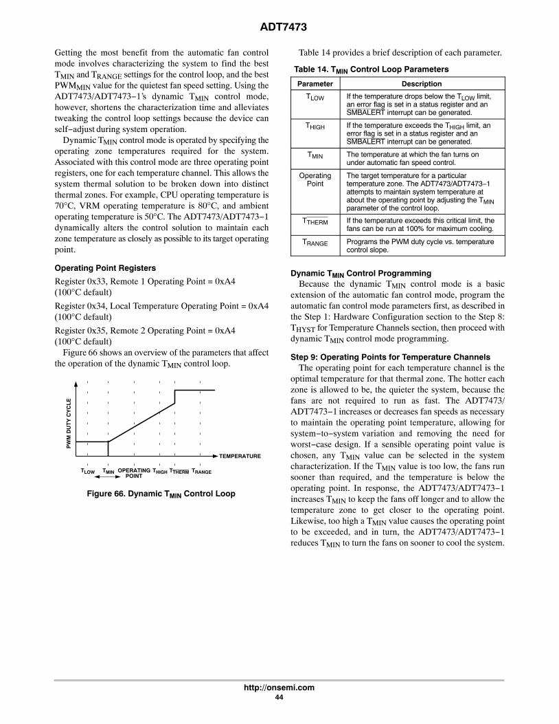
ADT7473
http://onsemi.com44
Getting the most benefit from the automatic fan controlmode involves characterizing the system to find the bestTMIN and TRANGE settings for the control loop, and the bestPWMMIN value for the quietest fan speed setting. Using theADT7473/ADT7473−1’s dynamic TMIN control mode,however, shortens the characterization time and alleviatestweaking the control loop settings because the device canself−adjust during system operation.
Dynamic TMIN control mode is operated by specifying theoperating zone temperatures required for the system.Associated with this control mode are three operating pointregisters, one for each temperature channel. This allows thesystem thermal solution to be broken down into distinctthermal zones. For example, CPU operating temperature is70°C, VRM operating temperature is 80°C, and ambientoperating temperature is 50°C. The ADT7473/ADT7473−1dynamically alters the control solution to maintain eachzone temperature as closely as possible to its target operatingpoint.
Operating Point Registers
Register 0x33, Remote 1 Operating Point = 0xA4(100°C default)
Register 0x34, Local Temperature Operating Point = 0xA4(100°C default)
Register 0x35, Remote 2 Operating Point = 0xA4(100°C default)
Figure 66 shows an overview of the parameters that affectthe operation of the dynamic TMIN control loop.
Figure 66. Dynamic TMIN Control Loop
PW
M D
UT
Y C
YC
LE
TLOW TMIN OPERATINGPOINT
THIGH TRANGE
TEMPERATURE
TTHERM
Table 14 provides a brief description of each parameter.
Table 14. TMIN Control Loop Parameters
Parameter Description
TLOW If the temperature drops below the TLOW limit,an error flag is set in a status register and anSMBALERT interrupt can be generated.
THIGH If the temperature exceeds the THIGH limit, anerror flag is set in a status register and anSMBALERT interrupt can be generated.
TMIN The temperature at which the fan turns onunder automatic fan speed control.
OperatingPoint
The target temperature for a particulartemperature zone. The ADT7473/ADT7473−1attempts to maintain system temperature atabout the operating point by adjusting the TMINparameter of the control loop.
TTHERM If the temperature exceeds this critical limit, thefans can be run at 100% for maximum cooling.
TRANGE Programs the PWM duty cycle vs. temperaturecontrol slope.
Dynamic TMIN Control ProgrammingBecause the dynamic TMIN control mode is a basic
extension of the automatic fan control mode, program theautomatic fan control mode parameters first, as described inthe Step 1: Hardware Configuration section to the Step 8:THYST for Temperature Channels section, then proceed withdynamic TMIN control mode programming.
Step 9: Operating Points for Temperature ChannelsThe operating point for each temperature channel is the
optimal temperature for that thermal zone. The hotter eachzone is allowed to be, the quieter the system, because thefans are not required to run as fast. The ADT7473/ADT7473−1 increases or decreases fan speeds as necessaryto maintain the operating point temperature, allowing forsystem−to−system variation and removing the need forworst−case design. If a sensible operating point value ischosen, any TMIN value can be selected in the systemcharacterization. If the TMIN value is too low, the fans runsooner than required, and the temperature is below theoperating point. In response, the ADT7473/ADT7473−1increases TMIN to keep the fans off longer and to allow thetemperature zone to get closer to the operating point.Likewise, too high a TMIN value causes the operating pointto be exceeded, and in turn, the ADT7473/ADT7473−1reduces TMIN to turn the fans on sooner to cool the system.

ADT7473
http://onsemi.com45
Programming Operating Point RegistersThere are three operating point registers, one for each
temperature channel. These 8−bit registers allow theoperating point temperatures to be programmed with 1°Cresolution.
Operating Point Registers
Register 0x33, Remote 1 Operating Point = 0xA4(100°C default)
Register 0x34, Local Operating Point = 0xA4(100°C default)
Register 0x35, Remote 2 Operating Point = 0xA4(100°C default).
Figure 67. Operating Point Value Dynamically Adjusts Automatic Fan Control Settings
Step 10: High and Low Limits for TemperatureChannels
The low limit defines the temperature at which the TMINvalue starts to be increased, if temperature falls below thisvalue. This has the net effect of reducing the fan speed,allowing the system to get hotter. An interrupt can begenerated when the temperature drops below the low limit.
The high limit defines the temperature at which the TMINvalue starts to be reduced, if temperature increases abovethis value. This has the net effect of increasing fan speed tocool down the system. An interrupt can be generated whenthe temperature rises above the high limit.
Programming High and Low LimitsThere are six limit registers; a high limit and low limit are
associated with each temperature channel. These 8−bitregisters allow the high and low limit temperatures to beprogrammed with 1°C resolution.
Temperature Limit Registers
Register 0x4E, Remote 1 Temperature Low Limit = 0x01
Register 0x4F, Remote 1 Temperature High Limit = 0x7F
Register 0x50, Local Temperature Low Limit = 0x01
Register 0x51, Local Temperature High Limit = 0x7F
Register 0x52, Remote 2 Temperature Low Limit = 0x01
Register 0x53, Remote 2 Temperature High Limit = 0x7F
How Dynamic TMIN Control WorksThe basic premise is as follows:
1. Set the target temperature for the temperaturezone, which could be, for example, the Remote 1thermal diode. This value is programmed to theRemote 1 operating temperature register.
2. As the temperature in that zone (Remote 1temperature) rises toward and exceeds theoperating point temperature, TMIN is reduced, andthe fan speed increases.
3. As the temperature drops below the operatingpoint temperature, TMIN is increased, and the fanspeed is reduced.
However, the loop operation is not as simple as describedin these steps. A number of conditions govern the situationsin which TMIN can increase or decrease.

ADT7473
http://onsemi.com46
Short Cycle and Long CycleThe ADT7473/ADT7473−1 implements two loops: a
short cycle and a long cycle. The short cycle takes placeevery n monitoring cycles. The long cycle takes place every2n monitoring cycles. The value of n is programmable foreach temperature channel. The bits are located at thefollowing register locations:
Remote 1 = CYR1 = Bits [2:0] of Dynamic TMIN ControlRegister 2 (0x37).
Local = CYL = Bits [5:3] of Dynamic TMIN Control Register 2(0x37).
Remote 2 = CYR2 = Bits [7:6] of Dynamic TMIN ControlRegister 2 (0x37) and Bit 0 of Dynamic TMIN ControlRegister 1 (0x36).
Table 15. Cycle Bit Assignments
Code Short Cycle Secs Long Cycle Secs
000 8 cycles 1 sec 16 cycles 2 sec
001 16 cycles 2 sec 32 cycles 4 sec
010 32 cycles 4 sec 64 cycles 8 sec
011 64 cycles 8 sec 128 cycles 16 sec
100 128 cycles 16 sec 256 cycles 32 sec
101 256 cycles 32 sec 512 cycles 64 sec
110 512 cycles 64 sec 1024 cycles 128 sec
111 1024 cycles 128 sec 2048 cycles 256 sec
Care should be taken when choosing the cycle time. Along cycle time means that TMIN is updated less often. Ifyour system has very fast temperature transients, thedynamic TMIN control loop is always lagging. If a cycle timeis chosen that is too fast, the full benefit of changing TMINmight not be realized and needs to change again on the nextcycle; in effect, it is overshooting. It is necessary to carry outsome calibration to identify the most suitable response time.
Figure 68 shows the steps taken during the short cycle.
Figure 68. Short Cycle Steps
IS T1(n) - T1(n - 1) = 0.5 - 0.75C
IS T1(n) - T1(n - 1) = 1.0 - 1.75C
IS T1(n) - T1(n - 1) > 2.0C
IS T1(n) >(OP1 − HYS)
YES
IS T1(n) − T1(n − 1)≤ 0.25C
DO NOTHING(SYSTEM IS
COOLING OFFFOR CONSTANT)
YES
NO
NODO NOTHING
WAIT nMONITORING
CYCLES
PREVIOUSTEMPERATUREMEASUREMENT
T1 (n − 1)
CURRENTTEMPERATUREMEASUREMENT
T1(n)
OPERATING POINT
TEMPERATUREOP1
DECREASE TMIN BY 1C
DECREASE TMIN BY 2C
DECREASE TMIN BY 4C
Figure 69 shows the steps taken during the long cycle.
Figure 69. Long Cycle Steps
WAIT 2nMONITORING
CYCLES
IS T1(n) < LOW TEMP LIMITAND
TMIN < HIGH TEMP LIMITAND
TMIN < OP1AND
T1(n) > TMIN
IS T1(n) > OP1YES
INCREASETMIN BY 1C
YES
NO
NO
DECREASE TMINBY 1C
CURRENTTEMPERATUREMEASUREMENT
T1(n)
OPERATING POINT
TEMPERATUREOP1
DO NOTCHANGE
The following examples illustrate some of thecircumstances that might cause TMIN to increase, decrease,or stay the same.
Example 1: Normal Operation—No TMIN Adjustment• If measured temperature never exceeds the
programmed operating point minus the hysteresistemperature, then TMIN is not adjusted; that is, itremains at its current setting.
• If measured temperature never drops below the lowtemperature limit, then TMIN is not adjusted.
Figure 70. Temperature Between Operating Pointand Low Temperature Limit
TMIN
THERM LIMIT
OPERATINGPOINT
HIGH TEMPLIMIT
LOW TEMPLIMIT
ACTUALTEMP
HYSTERESIS
Because neither the operating point minus the hysteresistemperature nor the low temperature limit has beenexceeded, the TMIN value is not adjusted, and the fan runs ata speed determined by the fixed TMIN and TRANGE valuesdefined in the automatic fan speed control mode.
Example 2: Operating Point Exceeded—TMIN ReducedWhen the measured temperature is below the operating
point temperature minus the hysteresis, TMIN remains thesame.
Once the temperature exceeds the operating temperatureminus the hysteresis (OP − Hyst), TMIN starts to decrease.This occurs during the short cycle (see Figure 68). The rate

ADT7473
http://onsemi.com47
at which TMIN decreases depends on the programmed valueof n. It also depends on how much the temperature hasincreased between this monitoring cycle and the lastmonitoring cycle; that is, if the temperature has increased by1°C, then TMIN is reduced by 2°C. Decreasing TMIN has theeffect of increasing the fan speed, thus providing morecooling to the system.
If the temperature slowly increases only in the range(OP − Hyst), that is, ≤0.25°C per short monitoring cycle,then TMIN does not decrease. This allows small changes intemperature in the desired operating zone without changingTMIN. The long cycle makes no change to TMIN in thetemperature range (OP − Hyst) because the temperature hasnot exceeded the operating temperature.
Once the temperature exceeds the operating temperature,the long cycle causes TMIN to be reduced by 1°C every longcycle while the temperature remains above the operatingtemperature. This takes place in addition to the decrease inTMIN that occurs due to the short cycle. In Figure 71, becausethe temperature is increasing at a rate ≤0.25°C per short cycle,no reduction in TMIN takes place during the short cycle.
Once the temperature falls below the operatingtemperature, TMIN stays the same. Even when thetemperature starts to increase slowly, TMIN stays the samebecause the temperature increases at a rate ≤0.25°C per cycle.
Example 3: Increase TMIN CycleWhen the temperature drops below the low temperature
limit, TMIN can increase in the long cycle. Increasing TMINhas the effect of running the fan slower and, therefore,quieter. The long cycle diagram in Figure 69 shows theconditions required for TMIN to increase. A quick summaryof those conditions and the reasons they need to be truefollows.
TMIN can increase if:• The measured temperature falls below the low temperature
limit. This means the user must choose the low limitcarefully. It should not be so low that the temperaturenever falls below it because TMIN would never increase,and the fans would run faster than necessary.
• TMIN is below the high temperature limit. TMIN isnever allowed to increase above the high temperaturelimit. As a result, the high limit should be sensiblychosen because it determines how high TMIN can go.
• TMIN is below the operating point temperature. TMINshould never be allowed to increase above the operatingpoint temperature because the fans would not switch onuntil the temperature rose above the operating point.
• The temperature is above TMIN. The dynamic TMINcontrol is turned off below TMIN.
Figure 71. Effect of Exceeding Operating Point MinusHysteresis Temperature
DECREASE HERE DUE TOSHORT CYCLE ONLY
T1(n) - T1 (n - 1) = 0.5C
OR 0.75C = > TMINDECREASES BY 1C
EVERY SHORT CYCLE
DECREASE HERE DUE TOLONG CYCLE ONLY
T1(n) - T1 (n - 1) ≤ 0.25C
AND T1(n) > OP = > TMINDECREASES BY 1C
EVERY LONG CYCLE
TMIN
THERMLIMIT
OPERATINGPOINT
HIGH TEMPLIMIT
LOW TEMPLIMIT
HYSTERESIS
NO CHANGE IN TMIN HEREDUE TO ANY CYCLE BECAUSE
T1(n) - T1 (n - 1) ≤ 0.25C
AND T1(n) < OP = > TMINSTAYS THE SAME
ACTUALTEMP
Figure 72 shows how TMIN increases when the currenttemperature is above TMIN and below the low temperaturelimit, and TMIN is below the high temperature limit andbelow the operating point. Once the temperature rises abovethe low temperature limit, TMIN stays the same.
Figure 72. Increasing TMIN for Quieter Operation
TMIN
OPERATINGPOINT
HIGH TEMPLIMIT
LOW TEMPLIMIT
ACTUALTEMP
HYSTERESIS
THERMLIMIT
Example 4: Preventing TMIN from Reaching Full ScaleBecause TMIN is dynamically adjusted, it is undesirable
for TMIN to reach full scale (127°C) because the fan wouldnever switch on. As a result, TMIN is allowed to vary onlywithin a specified range:• The lowest possible value for TMIN is −127°C (twos
complement mode) or −64°C (Offset 64 mode).• TMIN cannot exceed the high temperature limit.
• If the temperature is below TMIN, the fan is switchedoff or runs at minimum speed and dynamic TMINcontrol is disabled.

ADT7473
http://onsemi.com48
Figure 73. TMIN Adjustments Limited by the HighTemperature Limit
TMIN PREVENTEDFROM INCREASING
TMIN
OPERATINGPOINT
HIGH TEMPLIMIT
LOW TEMPLIMIT
ACTUALTEMP
HYSTERESIS
THERMLIMIT
Step 11: Monitoring THERMUsing the operating point limit ensures that the dynamic
TMIN control mode operates in the best possible acousticposition while ensuring that the temperature never exceedsthe maximum operating temperature. Using the operatingpoint limit allows TMIN to be independent of system−levelissues because of its self−corrective nature. In PC design, theoperating point for the chassis is usually the worst−caseinternal chassis temperature.
The optimal operating point for the processor isdetermined by monitoring the thermal monitor in the IntelPentium 4 processor. To do this, the PROCHOT output ofthe Pentium 4 is connected to the THERM input of theADT7473/ADT7473−1.
The operating point for the processor can be determinedby allowing the current temperature to be copied to theoperating point register when the PROCHOT output pullsthe THERM input low on the ADT7473/ADT7473−1. Thisgives the maximum temperature at which the Pentium 4 canrun before clock modulation occurs.
Enabling the THERM Trip Point as the Operating Point
Bits [4:2] of Dynamic TMIN Control Register 1 (0x36)enable/disable THERM monitoring to program theoperating point.
Dynamic TMIN Control Register 1 (0x36)
Bit [4] PHTR2 = 1, copies the Remote 2 current temperatureto the Remote 2 operating point register, if THERM isasserted. The operating point contains the temperature atwhich THERM is asserted. This allows the system to run asquietly as possible without affecting system performance.
PHTR2 = 0, ignores any THERM assertions. The Remote 2operating point register reflects its programmed value.
Bit [3] PHTL = 1, copies the local current temperature to thelocal temperature operating point register if THERM isasserted. The operating point contains the temperature atwhich THERM is asserted. This allows the system to run asquietly as possible without affecting system performance.
PHTL = 0, ignores any THERM assertions. The localtemperature operating point register reflects its programmedvalue.
Bit [2] PHTR1 = 1, copies the Remote 1 current temperatureto the Remote 1 operating point register if THERM isasserted. The operating point contains the temperature atwhich THERM is asserted. This allows the system to run asquietly as possible without affecting system performance.
PHTR1 = 0, ignores any THERM assertions. The Remote 1operating point register reflects its programmed value.
Enabling Dynamic TMIN Control Mode
Bits [7:5] of the Dynamic TMIN Control Register 1 (0x36)enable/disable dynamic TMIN control on the temperaturechannels.
Dynamic TMIN Control Register 1 (0x36)
Bit [7] R2T = 1, enables dynamic TMIN control on theRemote 2 temperature channel. The chosen TMIN value isdynamically adjusted based on the current temperature,operating point, and high and low limits for this zone.
R2T = 0, disables dynamic TMIN control. The TMIN valuechosen is not adjusted and the channel behaves as describedin the Automatic Fan Control Overview section.
Bit [6] LT = 1, enables dynamic TMIN control on the localtemperature channel. The chosen TMIN value is dynamicallyadjusted based on the current temperature, operating point,and high and low limits for this zone.
LT = 0, disables dynamic TMIN control. The TMIN valuechosen is not adjusted and the channel behaves as describedin the Automatic Fan Control Overview section.
Bit [5] R1T = 1, enables dynamic TMIN control on theRemote 1 temperature channel. The chosen TMIN value isdynamically adjusted based on the current temperature,operating point, and high and low limits for this zone.
R1T = 0, disables dynamic TMIN control. The TMIN valuechosen is not adjusted, and the channel behaves as describedin the Automatic Fan Control Overview section.
Enhancing System AcousticsAutomatic fan speed control mode reacts instantaneously
to changes in temperature; that is, the PWM duty cycleresponds immediately to temperature change. Any impulsesin temperature can cause an impulse in fan noise. Forpsycho−acoustic reasons, the ADT7473/ADT7473−1 canprevent the PWM output from reacting instantaneously totemperature changes. Enhanced acoustic mode controls themaximum change in PWM duty cycle at a given time. Theobjective is to prevent the fan from cycling up and down,annoying the user.
Acoustic Enhancement Mode OverviewFigure 74 gives a top−level overview of the automatic fan
control circuitry on the ADT7473/ADT7473−1 and showswhere acoustic enhancement fits in. Acoustic enhancementis intended as a post design tweak made by a system ormechanical engineer evaluating best settings for the system.Having determined the optimal settings for the thermal
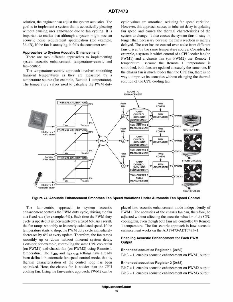
ADT7473
http://onsemi.com49
solution, the engineer can adjust the system acoustics. Thegoal is to implement a system that is acoustically pleasingwithout causing user annoyance due to fan cycling. It isimportant to realize that although a system might pass anacoustic noise requirement specification (for example,36 dB), if the fan is annoying, it fails the consumer test.
Approaches to System Acoustic EnhancementThere are two different approaches to implementing
system acoustic enhancement: temperature−centric andfan−centric.
The temperature−centric approach involves smoothingtransient temperatures as they are measured by atemperature source (for example, Remote 1 temperature).The temperature values used to calculate the PWM duty
cycle values are smoothed, reducing fan speed variation.However, this approach causes an inherent delay in updatingfan speed and causes the thermal characteristics of thesystem to change. It also causes the system fans to stay onlonger than necessary because the fan’s reaction is merelydelayed. The user has no control over noise from differentfans driven by the same temperature source. Consider, forexample, a system in which control of a CPU cooler fan (onPWM1) and a chassis fan (on PWM2) use Remote 1temperature. Because the Remote 1 temperature issmoothed, both fans are updated at exactly the same rate. Ifthe chassis fan is much louder than the CPU fan, there is noway to improve its acoustics without changing the thermalsolution of the CPU cooling fan.
Figure 74. Acoustic Enhancement Smoothes Fan Speed Variations Under Automatic Fan Speed Control
The fan−centric approach to system acousticenhancement controls the PWM duty cycle, driving the fanat a fixed rate (for example, 6%). Each time the PWM dutycycle is updated, it is incremented by a fixed 6%. As a result,the fan ramps smoothly to its newly calculated speed. If thetemperature starts to drop, the PWM duty cycle immediatelydecreases by 6% at every update. Therefore, the fan rampssmoothly up or down without inherent system delay.Consider, for example, controlling the same CPU cooler fan(on PWM1) and chassis fan (on PWM2) using Remote 1temperature. The TMIN and TRANGE settings have alreadybeen defined in automatic fan speed control mode, that is,thermal characterization of the control loop has beenoptimized. Here, the chassis fan is noisier than the CPUcooling fan. Using the fan−centric approach, PWM2 can be
placed into acoustic enhancement mode independently ofPWM1. The acoustics of the chassis fan can, therefore, beadjusted without affecting the acoustic behavior of the CPUcooling fan, even though both fans are controlled by Remote1 temperature. The fan−centric approach is how acousticenhancement works on the ADT7473/ADT7473−1.
Enabling Acoustic Enhancement for Each PWMOutput
Enhanced acoustics Register 1 (0x62)
Bit 3 = 1, enables acoustic enhancement on PWM1 output
Enhanced acoustics Register 2 (0x63)
Bit 7 = 1, enables acoustic enhancement on PWM2 outputBit 3 = 1, enables acoustic enhancement on PWM3 output

ADT7473
http://onsemi.com50
Effect of Ramp Rate on Enhanced Acoustics ModeThe PWM signal driving the fan has a period, T, given by
the PWM drive frequency, f, because T = 1/f. For a givenPWM period, T, the PWM period is subdivided into 255equal time slots. One time slot corresponds to the smallestpossible increment in the PWM duty cycle. A PWM signalof 33% duty cycle is, therefore, high for 1/3 x 255 time slotsand low for 2/3 x 255 time slots. Therefore, a 33% PWMduty cycle corresponds to a signal that is high for 85 timeslots and low for 170 time slots.
170TIME SLOTS
85TIME SLOTS
PWM OUTPUT(ONE PERIOD)
= 255 TIME SLOTS
PWM_OUT33% DUTY
CYCLE
Figure 75. 33% PWM Duty Cycle Representedin Time Slots
The ramp rates in the enhanced acoustics mode areselectable from the values 1, 2, 3, 5, 8, 12, 24, and 48. Theramp rates are discrete time slots. For example, if the ramprate is 8, then eight time slots are added to the PWM high dutycycle each time the PWM duty cycle needs to be increased.If the PWM duty cycle value needs to be decreased, it isdecreased by eight time slots. Figure 76 shows how theenhanced acoustics mode algorithm operates.
The enhanced acoustics mode algorithm calculates a newPWM duty cycle based on the temperature measured. If thenew PWM duty cycle value is greater than the previousPWM value, then the previous PWM duty cycle value isincremented by either 1, 2, 3, 5, 8, 12, 24, or 48 time slots,depending on the settings of the enhanced acousticsregisters. If the new PWM duty cycle value is less than theprevious PWM value, the previous PWM duty cycle isdecremented by 1, 2, 3, 5, 8, 12, 24, or 48 time slots. Eachtime the PWM duty cycle is incremented or decremented, itsvalue is stored as the previous PWM duty cycle for the nextcomparison. A ramp rate of 1 corresponds to one time slot,which is 1/255 of the PWM period. In enhanced acousticsmode, incrementing or decrementing by 1 changes the PWMoutput by 1/255 x 100%.
Figure 76. Enhanced Acoustics Algorithm
READTEMPERATURE
CALCULATENEW PWM
DUTY CYCLE
IS NEW PWMVALUE >
PREVIOUSVALUE?
INCREMENTPREVIOUS
PWM VALUEBY RAMP RATE
YES
NODECREMENT
PREVIOUSPWM VALUE
BY RAMP RATE
Step 12: Ramp Rate for Acoustic EnhancementThe optimal ramp rate for acoustic enhancement can be
found through system characterization after the thermaloptimization has been finished. The effect of each ramp rateshould be logged, if possible, to determine the best settingfor a given solution.
Enhanced Acoustics Register 1 (0x62)
Bits [2:0] ACOU, select the ramp rate for PWM1.000 = 1 time slot = 35 sec001 = 2 time slots = 17.6 sec010 = 3 time slots = 11.8 sec011 = 5 time slots = 7 sec100 = 8 time slots = 4.4 sec101 = 12 time slots = 3 sec110 = 24 time slots = 1.6 sec111 = 48 time slots = 0.8 sec
Enhanced Acoustics Register 2 (0x63)
Bits [2:0] ACOU3, select the ramp rate for PWM3.000 = 1 time slot = 35 sec001 = 2 time slots = 17.6 sec010 = 3 time slots = 11.8 sec011 = 5 time slots = 7 sec100 = 8 time slots = 4.4 sec101 = 12 time slots = 3 sec110 = 24 time slots = 1.6 sec111 = 48 time slots = 0.8 sec
Bits [6:4] ACOU2, select the ramp rate for PWM2.000 = 1 time slot = 35 sec001 = 2 time slots = 17.6 sec010 = 3 time slots = 11.8 sec011 = 5 time slots = 7 sec100 = 8 time slots = 4.4 sec101 = 12 time slots = 3 sec110 = 24 time slots = 1.6 sec111 = 48 time slots = 0.8 sec

ADT7473
http://onsemi.com51
Another way to view the ramp rates is to measure the timeit takes for the PWM output to ramp up from 0% to 100%duty cycle for an instantaneous change in temperature. Thiscan be tested by putting the ADT7473/ADT7473−1 intomanual mode and changing the PWM output from 0% to100% PWM duty cycle. The PWM output takes 35 secondsto reach 100% when a ramp rate of 1 time slot is selected.
Figure 77 shows remote temperature plotted againstPWM duty cycle for enhanced acoustics mode. The ramprate is set to 48, which corresponds to the fastest ramp rate.Assume that a new temperature reading is available every115 ms. With these settings, it takes approximately 0.76seconds to go from 33% duty cycle to 100% duty cycle (fullspeed). Even though the temperature increases very rapidly,the fan ramps up to full speed gradually.
Figure 77. Enhanced Acoustics Mode withRamp Rate = 48
TIME (s)
140
0 0.76
120
100
80
60
40
20
0
120
100
80
60
40
20
0
RTEMP (C)
PWM CYCLE (%)
RT
EM
P (C
)
PW
M C
YC
LE
(%
)
Figure 78 shows how changing the ramp rate from 48 to8 affects the control loop. The overall response of the fan isslower. Because the ramp rate is reduced, it takes longer forthe fan to achieve full running speed. In this case, it takesapproximately 4.4 seconds for the fan to reach full speed.
Figure 78. Enhanced Acoustics Mode withRamp Rate = 8
TIME (s)
120
0 4.4
140
120
100
80
60
40
0
20
100
80
60
40
20
0
RTEMP (C)
PWM DUTY CYCLE (%)
RT
EM
P (C
)
PW
M D
UT
Y C
YC
LE
(%
)
Figure 79 shows the PWM output response for a ramp rateof 2. In this instance, the fan takes about 17.6 seconds toreach full running speed.
Figure 79. Enhanced Acoustics Mode withRamp Rate = 2
TIME (s)
140
0 17.6
120
100
80
60
40
20
0
120
100
80
60
40
20
0
RTEMP (C)
RT
EM
P (C
)
PWM DUTY CYCLE (%)
PW
M D
UT
Y C
YC
LE
(%
)
Figure 80 shows how the control loop reacts totemperature with the slowest ramp rate. The ramp rate is setto 1, while all other control parameters remain the same.With the slowest ramp rate selected, it takes 35 seconds forthe fan to reach full speed.
Figure 80. Enhanced Acoustics Mode withRamp Rate = 1
TIME (s)0 35
120
100
80
60
40
20
0
140120
100
80
60
40
20
0
RTEMP (C)
RT
EM
P (C
)
PWM DUTY CYCLE (%)
PW
M D
UT
Y C
YC
LE
(%
)As Figure 77 to Figure 80 show, the rate at which the fan
reacts to temperature change is dependent on the ramp rateselected in the enhanced acoustics registers. The higher theramp rate, the faster the fan reaches the newly calculated fanspeed.
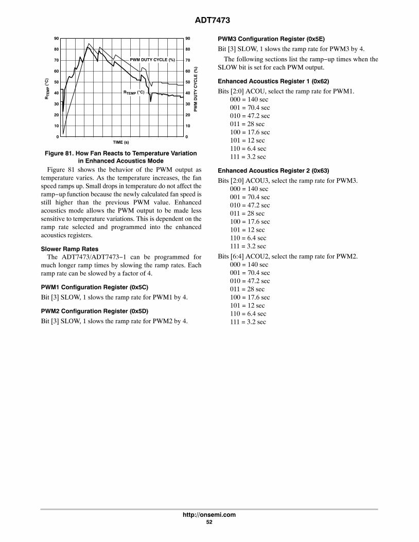
ADT7473
http://onsemi.com52
Figure 81. How Fan Reacts to Temperature Variationin Enhanced Acoustics Mode
90
80
70
60
50
40
0
30
20
10
90
80
70
60
50
40
0
30
20
10
PWM DUTY CYCLE (%)
RTEMP (C)
TIME (s)
RT
EM
P (C
)
PW
M D
UT
Y C
YC
LE
(%
)
Figure 81 shows the behavior of the PWM output astemperature varies. As the temperature increases, the fanspeed ramps up. Small drops in temperature do not affect theramp−up function because the newly calculated fan speed isstill higher than the previous PWM value. Enhancedacoustics mode allows the PWM output to be made lesssensitive to temperature variations. This is dependent on theramp rate selected and programmed into the enhancedacoustics registers.
Slower Ramp RatesThe ADT7473/ADT7473−1 can be programmed for
much longer ramp times by slowing the ramp rates. Eachramp rate can be slowed by a factor of 4.
PWM1 Configuration Register (0x5C)
Bit [3] SLOW, 1 slows the ramp rate for PWM1 by 4.
PWM2 Configuration Register (0x5D)
Bit [3] SLOW, 1 slows the ramp rate for PWM2 by 4.
PWM3 Configuration Register (0x5E)
Bit [3] SLOW, 1 slows the ramp rate for PWM3 by 4.
The following sections list the ramp−up times when theSLOW bit is set for each PWM output.
Enhanced Acoustics Register 1 (0x62)
Bits [2:0] ACOU, select the ramp rate for PWM1.000 = 140 sec001 = 70.4 sec010 = 47.2 sec011 = 28 sec100 = 17.6 sec101 = 12 sec110 = 6.4 sec111 = 3.2 sec
Enhanced Acoustics Register 2 (0x63)
Bits [2:0] ACOU3, select the ramp rate for PWM3.000 = 140 sec001 = 70.4 sec010 = 47.2 sec011 = 28 sec100 = 17.6 sec101 = 12 sec110 = 6.4 sec111 = 3.2 sec
Bits [6:4] ACOU2, select the ramp rate for PWM2.000 = 140 sec001 = 70.4 sec010 = 47.2 sec011 = 28 sec100 = 17.6 sec101 = 12 sec110 = 6.4 sec111 = 3.2 sec

ADT7473
http://onsemi.com53
Register Tables
Table 16. ADT7473/ADT7473−1 Registers
Addr R/W Desc Bit 7 Bit 6 Bit 5 Bit 4 Bit 3 Bit 2 Bit 1 Bit 0 De-fault
Lock-able
0x21 R VCCPReading
9 8 7 6 5 4 3 2 0x00 −
0x22 R VCCReading
9 8 7 6 5 4 3 2 0x00 −
0x25 R Remote 1Temp.
9 8 7 6 5 4 3 2 0x01 −
0x26 R LocalTemp.
9 8 7 6 5 4 3 2 0x01 −
0x27 R Remote 2Temp.
9 8 7 6 5 4 3 2 0x01 −
0x28 R TACH1 LowByte
7 6 5 4 3 2 1 0 0x00 −
0x29 R TACH1High Byte
15 14 13 12 11 10 9 8 0x00 −
0x2A R TACH2 LowByte
7 6 5 4 3 2 1 0 0x00 −
0x2B R TACH2High Byte
15 14 13 12 11 10 9 8 0x00 −
0x2C R TACH3 LowByte
7 6 5 4 3 2 1 0 0x00 −
0x2D R TACH3High Byte
15 14 13 12 11 10 9 8 0x00 −
0x2E R TACH4 LowByte
7 6 5 4 3 2 1 0 0x00 −
0x2F R TACH4High Byte
15 14 13 12 11 10 9 8 0x00 −
0x30 R/W PWM1Current
Duty Cycle
7 6 5 4 3 2 1 0 0x00/0xFF
−
0x31 R/W PWM2Current
Duty Cycle
7 6 5 4 3 2 1 0 0x00/0xFF
−
0x32 R/W PWM3Current
Duty Cycle
7 6 5 4 3 2 1 0 0x00/0xFF
−
0x33 R/W Remote 1Operating
Point
7 6 5 4 3 2 1 0 0xA4 Yes
0x34 R/W Local TempOperating
Point
7 6 5 4 3 2 1 0 0xA4 Yes
0x35 R/W Remote 2Operating
Point
7 6 5 4 3 2 1 0 0xA4 Yes
0x36 R/W DynamicTMIN
ControlReg. 1
R2T LT R1T PHTR2 PHTL PHTR1 VCCPLO CYR2 0x00 Yes
0x37 R/W DynamicTMIN
ControlReg. 2
CYR2 CYR2 CYL CYL CYL CYR1 CYR1 CYR1 0x00 Yes
0x38 R/W PWM1 MaxDuty Cycle
7 6 5 4 3 2 1 0 0xFF −
0x39 R/W PWM2 MaxDuty Cycle
7 6 5 4 3 2 1 0 0xFF −
0x3A R/W PWM3 MaxDuty Cycle
7 6 5 4 3 2 1 0 0xFF −

ADT7473
http://onsemi.com54
Table 16. ADT7473/ADT7473−1 Registers
Addr Lock-able
De-fault
Bit 0Bit 1Bit 2Bit 3Bit 4Bit 5Bit 6Bit 7DescR/W
0x3D R Device IDRegister
7 6 5 4 3 2 1 0 0x73 −
0x3E R CompanyID Number
7 6 5 4 3 2 1 0 0x41 −
0x3F R Revision IDRegister
7 6 5 4 3 2 1 0 0x68/0x69
−
0x40 R/W Config.Register 1
ADT7473:RES
ADT7473−1:Latch Reset
TODIS FSPDIS Vx1 FSPD RDY LOCK STRT 0x01 Yes
0x41 R InterruptStatus
Register 1
OOL R2T LT R1T RES VCC VCCP RES 0x00 −
0x42 R InterruptStatus
Register 2
D2 D1 F4P FAN3 FAN2 FAN1 OVT ADT7473:RES
ADT7473−1:THERM
Limit Latch
0x00 −
0x46 R/W VCCP LowLimit
7 6 5 4 3 2 1 0 0x00 −
0x47 R/W VCCP HighLimit
7 6 5 4 3 2 1 0 0xFF −
0x48 R/W VCC LowLimit
7 6 5 4 3 2 1 0 0x00 −
0x49 R/W VCC HighLimit
7 6 5 4 3 2 1 0 0xFF −
0x4E R/W Remote 1Temp. Low
Limit
7 6 5 4 3 2 1 0 0x01 −
0x4F R/W Remote 1Temp. High
Limit
7 6 5 4 3 2 1 0 0xFF −
0x50 R/W Local Temp.Low Limit
7 6 5 4 3 2 1 0 0x01 −
0x51 R/W Local Temp.High Limit
7 6 5 4 3 2 1 0 0xFF −
0x52 R/W Remote 2Temp. Low
Limit
7 6 5 4 3 2 1 0 0x01 −
0x53 R/W Remote 2Temp. High
Limit
7 6 5 4 3 2 1 0 0xFF −
0x54 R/W TACH1MinimumLow Byte
7 6 5 4 3 2 1 0 0xFF −
0x55 R/W TACH1MinimumHigh Byte
15 14 13 12 11 10 9 8 0xFF −
0x56 R/W TACH2MinimumLow Byte
7 6 5 4 3 2 1 0 0xFF −
0x57 R/W TACH2MinimumHigh Byte
15 14 13 12 11 10 9 8 0xFF −
0x58 R/W TACH3MinimumLow Byte
7 6 5 4 3 2 1 0 0xFF −
0x59 R/W TACH3MinimumHigh Byte
15 14 13 12 11 10 9 8 0xFF −

ADT7473
http://onsemi.com55
Table 16. ADT7473/ADT7473−1 Registers
Addr Lock-able
De-fault
Bit 0Bit 1Bit 2Bit 3Bit 4Bit 5Bit 6Bit 7DescR/W
0x5A R/W TACH4MinimumLow Byte
7 6 5 4 3 2 1 0 0xFF −
0x5B R/W TACH4MinimumHigh Byte
15 14 13 12 11 10 9 8 0xFF −
0x5C R/W PWM1Config.Register
BHVR BHVR BHVR INV SLOW SPIN SPIN SPIN 0x82/0x62
Yes
0x5D R/W PWM2Config.Register
BHVR BHVR BHVR INV SLOW SPIN SPIN SPIN 0x82/0x62
Yes
0x5E R/W PWM3Config.Register
BHVR BHVR BHVR INV SLOW SPIN SPIN SPIN 0x82/0x62
Yes
0x5F R/W Remote 1TRANGE/PWM 1
Frequency
RANGE RANGE RANGE RANGE HF/LFFan 1
FREQ FREQ FREQ 0xCC Yes
0x60 R/W LocalTRANGE/PWM 2
Frequency
RANGE RANGE RANGE RANGE HF/LFFan 2
FREQ FREQ FREQ 0xCC Yes
0x61 R/W Remote 2TRANGE/PWM 3
Frequency
RANGE RANGE RANGE RANGE HF/LFFan 3
FREQ FREQ FREQ 0xCC Yes
0x62 R/W EnhancedAcoustics
Reg. 1
MIN3 MIN2 MIN1 SYNC EN1 ACOU ACOU ACOU 0x00 Yes
0x63 R/W EnhancedAcoustics
Reg. 2
EN2 ACOU2 ACOU2 ACOU2 EN3 ACOU3 ACOU3 ACOU3 0x00 Yes
0x64 R/W PWM1 Min Duty Cycle
7 6 5 4 3 2 1 0 0x80 Yes
0x65 R/W PWM2 Min Duty Cycle
7 6 5 4 3 2 1 0 0x80 Yes
0x66 R/W PWM3 Min Duty Cycle
7 6 5 4 3 2 1 0 0x80 Yes
0x67 R/W Remote 1 Temp. TMIN
7 6 5 4 3 2 1 0 0x9A Yes
0x68 R/W Local Temp.TMIN
7 6 5 4 3 2 1 0 0x9A Yes
0x69 R/W Remote 2 Temp. TMIN
7 6 5 4 3 2 1 0 0x9A Yes
0x6A R/W Remote 1THERM
Temp. Limit
7 6 5 4 3 2 1 0 0xA4 Yes
0x6B R/W LocalTHERM
Temp. Limit
7 6 5 4 3 2 1 0 0xA4 Yes
0x6C R/W Remote 2THERM
Temp. Limit
7 6 5 4 3 2 1 0 0xA4/0xC8
Yes
0x6D R/W Remote 1and LocalTemp/TMINHysteresis
HYSR1 HYSR1 HYSR1 HYSR1 HYSL HYSL HYSL HYSL 0x44 Yes
0x6E R/W Remote 2Temp/TMINHysteresis
HYSR2 HYSR2 HYSR2 HYRS2 RES RES RES RES 0x40 Yes
0x6F R/W XNOR TreeTest Enable
RES RES RES RES RES RES RES XEN 0x00 Yes

ADT7473
http://onsemi.com56
Table 16. ADT7473/ADT7473−1 Registers
Addr Lock-able
De-fault
Bit 0Bit 1Bit 2Bit 3Bit 4Bit 5Bit 6Bit 7DescR/W
0x70 R/W Remote 1Temp.Offset
7 6 5 4 3 2 1 0 0x00 Yes
0x71 R/W Local Temp.Offset
7 6 5 4 3 2 1 0 0x00 Yes
0x72 R/W Remote 2Temp.Offset
7 6 5 4 3 2 1 0 0x00 Yes
0x73 R/W Config.Register 2
SHDN CONV ATTN AVG FAN3Detect
FAN2Detect
FAN1Detect
FANPresence
DT
0x00 Yes
0x74 R/W InterruptMask
Register 1
OOL R2T LT R1T RES VCC VCCP RES 0x00 −
0x75 R/W InterruptMask
Register 2
D2 D1 F4P FAN3 FAN2 FAN1 OVT RES 0x00 −
0x76 R ExtendedResolution
1
RES RES VCC VCC VCCP VCCP RES RES 0x00 −
0x77 R ExtendedResolution
2
TDM2 TDM2 LTMP LTMP TDM1 TDM1 RES RES 0x00 −
0x78 R/W Config.Register 3
DC4 DC3 DC2 DC1 FAST BOOST THERM ALERTEnable
0x00 Yes
0x79 R THERMTimerStatus
Register
TMR TMR TMR TMR TMR TMR TMR ASRT/TMRO
0x00 −
0x7A R/W THERMTimer Limit
Register
LIMT LIMT LIMT LIMT LIMT LIMT LIMT LIMT 0x00 −
0x7B R/W TACHPulses perRevolution
FAN4 FAN4 FAN3 FAN3 FAN2 FAN2 FAN1 FAN1 0X55 −
0x7C R/W Config.Register 5
R2 THERM LocalTHERM
R1THERM
ADT7473: RES
ADT7473−1:THERM HYSTR
GPIOP GPIOD TempOffset
TWOSCOMPL
ADT7473:0x00
Yes
0x7D R/W Config.Register 4
RES RES BpAttVCCP
ADT7473: RESADT7473−1:
THERM_LATCHCONFIG
Max/Full on
THERM
THERMDisable
PIN9FUNC
PIN9FUNC
0x00 Yes
0x7E R TestRegister 1
Do not write to these registers 0x00 Yes
0x7F R TestRegister 2
Do not write to these registers 0x00 Yes
0x80 R TestRegister 3
Do not write to these registers 0x10 Yes
Table 17. Voltage Reading Registers (Power−On Default = 0x00) (Note 1)
Register Address R/W Description
0x21 Read−only Reflects the voltage measurement at the VCCP input on Pin 14 (8 MSB of reading). (Note 2)
0x22 Read−only Reflects the voltage measurement at the VCC input on Pin 3 (8 MSB of reading). (Note 3)
1. If the extended resolution bits of these readings are also being read, the extended resolution registers (Register 0x76 and Register 0x77)must be read first. Once the extended resolution registers have been read, the associated MSB reading registers are frozen until read.Both the extended resolution registers and the MSB registers are frozen.
2. If VCCPLO (Bit 1 of the Dynamic TMIN Control Register 1, 0x36) is set, VCCP can control the sleep state of the ADT7473/ADT7473−1.3. VCC (Pin 3) is the supply voltage for the ADT7473/ADT7473−1.

ADT7473
http://onsemi.com57
Table 18. Temperature Reading Registers (Power−On Default = 0x01) (Note 1 and 2)
Register Address R/W Description
0x25 Read−only Remote 1 temperature reading (8 MSB of reading). (Note 3 and 4)
0x26 Read−only Local temperature reading (8 MSB of reading).
0x27 Read−only Remote 2 temperature reading (8 MSB of reading). (Note 3 and 4)
1. These temperature readings can be in twos complement or Offset 64 format; this interpretation is determined by Bit 0 of ConfigurationRegister 5 (0x7C).
2. If the extended resolution bits of these readings are also being read, the extended resolution registers (Register 0x76 and Register 0x77)must be read first. Once the extended resolution registers have been read, all associated MSB reading registers are frozen until read. Boththe extended resolution registers and the MSB registers are frozen.
3. In twos complement mode, a temperature reading of −128°C (0x80) indicates a diode fault (open or short) on that channel.4. In Offset 64 mode, a temperature reading of −64°C (0x00) indicates a diode fault (open or short) on that channel.
Table 19. Fan Tachometer Reading Registers (Power−On Default = 0x00) (Note 1)
Register Address R/W Description
0x28 Read−only TACH1 low byte.
0x29 Read−only TACH1 high byte.
0x2A Read−only TACH2 low byte.
0x2B Read−only TACH2 high byte.
0x2C Read−only TACH3 low byte.
0x2D Read−only TACH3 high byte.
0x2E Read−only TACH4 low byte.
0x2F Read−only TACH4 high byte.
1. These registers count the number of 11.11 s periods (based on an internal 90 kHz clock) that occur between a number of consecutive fanTACH pulses (default = 2). The number of TACH pulses used to count can be changed using the TACH pulses per revolution register (Register0x7B). This allows the fan speed to be accurately measured. Because a valid fan tachometer reading requires that two bytes are read, thelow byte must be read first. Both the low and high bytes are then frozen until read. At power−on, these registers contain 0x0000 until the firstvalid fan TACH measurement is read into these registers. This prevents false interrupts from occurring while the fans are spinning up. A countof 0xFFFF indicates a fan is one of the following:• Stalled or blocked (object jamming the fan).• Failed (internal circuitry destroyed).• Not populated. (The ADT7473/ADT7473−1 expects to see a fan connected to each TACH. If a fan is not connected to that TACH, its TACHminimum high and low bytes should be set to 0xFFFF.)• Alternate function, for example, TACH4 reconfigured as THERM pin.
Table 20. Current PWM Duty Cycle Registers (ADT7473 Power−On Default = 0x00, ADT7473−1 Power−On Default = 0xFF) (Note 1)
Register Address R/W Description
0x30 R/W PWM1 current duty cycle (0% to 100% duty cycle = 0x00 to 0xFF).
0x31 R/W PWM2 current duty cycle (0% to 100% duty cycle = 0x00 to 0xFF).
0x32 R/W PWM3 current duty cycle (0% to 100% duty cycle = 0x00 to 0xFF).
1. These registers reflect the PWM duty cycle driving each fan at any given time. When in automatic fan speed control mode, theADT7473/ADT7473−1 reports the PWM duty cycles back through these registers. The PWM duty cycle values vary according totemperature in automatic fan speed control mode. During fan startup, these registers report back 0x00. In software mode, the PWM dutycycle outputs can be set to any duty cycle value by writing to these registers.
Table 21. Operating Point Registers (Power−On = 0xA4) (Note 1, 2 and 3)
Register Address R/W (Note 3) Description
0x33 R/W Remote 1 operating point register (default = 100°C).
0x34 R/W Local temperature operating point register (default = 100°C).
0x35 R/W Remote 2 operating point register (default = 100°C).
1. These registers set the target operating point for each temperature channel when the dynamic TMIN control feature is enabled.2. The fans being controlled are adjusted to maintain temperature about an operating point.3. These registers become read−only when the Configuration Register 1 lock bit is set to 1. Any subsequent attempts to write to these
registers fail.

ADT7473
http://onsemi.com58
Table 22. Register 0x36 — Dynamic TMIN Control Register 1 (Power−On Default = 0x00) (Note 1)
Bit No. Mnemonic R/W Description
[0] CYR2 R/W MSB of 3−bit remote 2 cycle value. The other two bits of the code reside in Dynamic TMINControl Register 2 (Reg. 0x37). These three bits define the delay time between makingsubsequent TMIN adjustments in the control loop, in terms of the number of monitoringcycles. The system has associated thermal time constants that need to be found to optimizethe response of fans and the control loop.
[1] VCCPLO R/W VCCPLO = 1. When the power is supplied from 3.3 V STANDBY and the core voltage (VCCP)drops below its VCCP low limit value (Register 0x46), the following occurs:
Status Bit 1 in Interrupt Status Register 1 is set.SMBALERT is generated, if enabled.PROCHOT monitoring is disabled.Dynamic TMIN control is disabled.The device is prevented from entering shutdown.Everything is re−enabled once VCCP increases above the VCCP low limit.
[2] PHTR1 R/W PHTR1 = 1 copies the Remote 1 current temperature to the Remote 1 operating pointregister if THERM is asserted. The operating point contains the temperature at whichTHERM is asserted, allowing the system to run as quietly as possible without affectingsystem performance. PHTR1 = 0 ignores any THERM assertions on the THERM pin. The Remote 1 operatingpoint register reflects its programmed value.
[3] PHTL R/W PHTL = 1 copies the local channel’s current temperature to the local operating point registerif THERM is asserted. The operating point contains the temperature at which THERM isasserted. This allows the system to run as quietly as possible without affecting systemperformance.PHTL = 0 ignores any THERM assertions on the THERM pin. The local temperatureoperating point register reflects its programmed value.
[4] PHTR2 R/W PHTR2 = 1 copies the Remote 2 current temperature to the Remote 2 operating pointregister if THERM is asserted. The operating point contains the temperature at whichTHERM is asserted, allowing the system to run as quietly as possible without affectingsystem performance.PHTR2 = 0 ignores any THERM assertions on the THERM pin. The Remote 2 operatingpoint register reflects its programmed value.
[5] R1T R/W R1T = 1 enables dynamic TMIN control on the Remote 1 temperature channel. The chosenTMIN value is dynamically adjusted based on the current temperature, operating point, andhigh and low limits for this zone.R1T = 0 disables dynamic TMIN control. The TMIN value chosen is not adjusted, and thechannel behaves as described in the Fan Speed Control section.
[6] LT R/W LT=1 enables dynamic TMIN control on the local temperature channel. The chosen TMINvalue is dynamically adjusted based on the current temperature, operating point, and highand low limits for this zone. LT = 0 disables dynamic TMIN control. The TMIN value chosen is not adjusted, and thechannel behaves as described in the Fan Speed Control section.
[7] R2T R/W R2T = 1 enables dynamic TMIN control on the Remote 2 temperature channel. The chosenTMIN value is dynamically adjusted based on the current temperature, operating point, andhigh and low limits for this zone. R2T = 0 disables dynamic TMIN control. The TMIN value chosen is not adjusted and thechannel behaves as described in the Fan Speed Control section.
1. This register becomes read−only when the Configuration Register 1 lock bit is set to 1. Any subsequent attempts to write to this register fail.

ADT7473
http://onsemi.com59
Table 23. Register 0x37 — Dynamic TMIN Control Register 2 (Power−On Default = 0x00) (Note 1)
Bit No. Mnemonic R/W Description
[2:0] CYR1 R/W 3−bit remote 1 cycle value. These three bits define the delay time between makingsubsequent TMIN adjustments in the control loop for the Remote 1 channel, in terms ofnumber of monitoring cycles. The system has associated thermal time constants that need tobe found to optimize the response of fans and the control loop.
Bits Decrease Cycle Increase Cycle
000 8 cycles (1 sec) 16 cycles (2 sec)
001 16 cycles (2 sec) 32 cycles (4 sec)
010 32 cycles (4 sec) 64 cycles (8 sec)
011 64 cycles (8 sec) 128 cycles (16 sec)
100 128 cycles (16 sec) 256 cycles (32 sec)
101 256 cycles (32 sec) 512 cycles (64 sec)
110 512 cycles (64 sec) 1024 cycles (128 sec)
111 1024 cycles (128 sec) 2048 cycles (256 sec)
[5:3] CYL R/W 3−bit local temperature cycle value. These three bits define the delay time between makingsubsequent TMIN adjustments in the control loop for the local temperature channel, in termsof number of monitoring cycles. The system has associated thermal time constants that needto be found to optimize the response of fans and the control loop.
Bits Decrease Cycle Increase Cycle
000 8 cycles (1 sec) 16 cycles (2 sec)
001 16 cycles (2 sec) 32 cycles (4 sec)
010 32 cycles (4 sec) 64 cycles (8 sec)
011 64 cycles (8 sec) 128 cycles (16 sec)
100 128 cycles (16 sec) 256 cycles (32 sec)
101 256 cycles (32 sec) 512 cycles (64 sec)
110 512 cycles (64 sec) 1024 cycles (128 sec)
111 1024 cycles (128 sec) 2048 cycles (256 sec)
[7:6] CYR2 R/W 2 LSBs of 3−bit remote 2 cycle value. The MSB of the 3−bit code resides in Dynamic TMINControl Register 1 (Register 0x36). These three bits define the delay time between makingsubsequent TMIN adjustments in the control loop for the Remote 2 channel, in terms ofnumber of monitoring cycles. The system has associated thermal time constants that need tobe found to optimize the response of fans and the control loop.
Bits Decrease Cycle Increase Cycle
000 8 cycles (1 sec) 16 cycles (2 sec)
001 16 cycles (2 sec) 32 cycles (4 sec)
010 32 cycles (4 sec) 64 cycles (8 sec)
011 64 cycles (8 sec) 128 cycles (16 sec)
100 128 cycles (16 sec) 256 cycles (32 sec)
101 256 cycles (32 sec) 512 cycles (64 sec)
110 512 cycles (64 sec) 1024 cycles (128 sec)
111 1024 cycles (128 sec) 2048 cycles (256 sec)
1. This register becomes read−only when the Configuration Register 1 lock bit is set to 1. Any subsequent attempts to write to this register fail.

ADT7473
http://onsemi.com60
Table 24. Maximum PWM Duty Cycle Registers (Power−On Default = 0xFF) (Note 1, 2, and 3)
Register Address R/W (Note 2) Description
0x38 R/W Maximum duty cycle for PWM1 output, default = 100% (0xFF).
0x39 R/W Maximum duty cycle for PWM2 output, default = 100% (0xFF).
0x3A R/W Maximum duty cycle for PWM3 output, default = 100% (0xFF).
1. These registers set the maximum PWM duty cycle of the PWM output.2. These registers become read−only when the Configuration Register 1 lock bit is set to 1. Any subsequent attempts to write to this register fail.3. If Bit 3 of Configuration Register 4 (0x7D) is set, then on a THERM overtemperature event, fans go to their maximum programmed PWM value
as programmed here. If Bit 3 of Configuration Register 4 (0x7D) is 0, then on a THERM overtemperature event, fans go to 100% PWM.
Table 25. Register 0x40 — Configuration Register 1 (Power−On Default = 0x01)
Bit No. Mnemonic R/W Description
[0] STRT R/W Logic 1 enables monitoring and PWM control outputs based on the limit settingsprogrammed. Logic 0 disables monitoring and PWM control based on the default poweruplimit settings. This bit is not locked when Bit 1 (LOCK bit) has been written. This bit remainswritable after lock bit is set.
[1] LOCK Write once Logic 1 locks all limit values to their current settings. Once this bit is set, all lockable registersbecome read−only and cannot be modified until the ADT7473/ADT7473−1 is powered downand powered up again. This prevents rogue programs, such as viruses, from modifyingcritical system limit settings. (This is a lockable bit.)
[2] RDY Read−only This bit is set to 1 by the ADT7473/ADT7473−1 to indicate only that the device is fullypowered up and ready to begin system monitoring.
[3] FSPD R/W When set to 1, this bit runs all fans at maximum speed as programmed in the maximumPWM duty cycle registers (0x30, 0x38, 0x39 and 0x3A ). Power−on default = 0. This bit is notlocked at any time.
[4] Vx1 R/W BIOS should set this bit to a 1 when the ADT7473/ADT7473−1 is configured to measurecurrent from an ADI ADOPT VRM controller and to measure the CPU’s core voltage. Thisbit allows monitoring software to display CPU watts usage. (This is a lockable bit.)
[5] FSPDIS R/W Logic 1 disables fan spin−up for two TACH pulses. Instead, the PWM outputs go high for theentire fan spin−up timeout selected.
[6] TODIS R/W When this bit is set to 1, the SMBus timeout feature is enabled. This allows theADT7473/ADT7473−1 to be used with SMBus controllers that cannot handle SMBustimeouts. (This is a lockable bit.)
[7] RESLatch Reset
Reserved on the ADT7473.On the ADT7473−1, resets latch conditions when set to 1.
Table 26. Register 0x41 — Interrupt Status Register 1 (Power−On Default = 0x00)
Bit No. Mnemonic R/W Description
[1] VCCP Read−only VCCP = 1 indicates the VCCP high or low limit has been exceeded. This bit is cleared on aread of the status register only if the error condition has subsided.
[2] VCC Read−only VCC = 1 indicates the VCC high or low limit has been exceeded. This bit is cleared on a readof the status register only if the error condition has subsided.
[4] R1T Read−only R1T = 1 indicates the Remote 1 low or high temperature has been exceeded. This bit iscleared on a read of the status register only if the error condition has subsided.
[5] LT Read−only LT = 1 indicates the local low or high temperature has been exceeded. This bit is cleared ona read of the status register only if the error condition has subsided.
[6] R2T Read−only R2T = 1 indicates the Remote 2 low or high temperature has been exceeded. This bit iscleared on a read of the status register only if the error condition has subsided.
[7] OOL Read−only OOL = 1 indicates an out−of−limit event has been latched in Interrupt Status Register 2(0x42). This bit is a logical OR of all status bits in Interrupt Status Register 2. Software cantest this bit in isolation to determine whether any of the voltage, temperature, or fan speedreadings represented by Interrupt Status Register 2 are out−of−limit, which saves the need toread Interrupt Status Register 2 every interrupt or polling cycle.

ADT7473
http://onsemi.com61
Table 27. Register 0x42 — Interrupt Status Register 2 (Power−On Default = 0x00)
Bit No. Mnemonic R/W Description
[0] RES Read−only Reserved on the ADT7473.
THERMLimit Latch
On the ADT7473−1, THERM Limit Latch = 1 indicates Remote Channel 2 latch. This is aTHERM limit condition.
[1] OVT Read−only OVT = 1 indicates one of the THERM overtemperature limits is exceeded. This bit is clearedon a read of the status register when the temperature drops below THERM – THYST.
[2] FAN1 Read−only FAN1 = 1 indicates Fan 1 has dropped below minimum speed or has stalled. This bit is notset when the PWM1 output is off.
[3] FAN2 Read−only FAN2 = 1 indicates Fan 2 has dropped below minimum speed or has stalled. This bit is notset when the PWM2 output is off.
[4] FAN3 Read−only FAN3 = 1 indicates Fan 3 has dropped below minimum speed or has stalled. This bit is notset when the PWM3 output is off.
[5] F4P Read−only F4P = 1 indicates Fan 4 has dropped below minimum speed or has stalled. This bit is not setwhen the PWM3 output is off.
R/W When Pin 9 is programmed as a GPIO output, writing to this bit determines the logic output ofthe GPIO.
Read−only If Pin 9 is configured as the THERM timer input for THERM monitoring, then this bit is setwhen the THERM assertion time exceeds the limit programmed in the THERM timer limitregister (Reg. 0x7A).
[6] D1 Read−only D1 = 1 indicates either an open or short circuit on the Thermal Diode 1 inputs.
[7] D2 Read−only D2 = 1 indicates either an open or short circuit on the Thermal Diode 2 inputs.
Table 28. Voltage Limit Registers (Note 1)
Register Address R/W Description (Note 2) Power−On Default
0x46 R/W VCCP low limit. 0x00
0x47 R/W VCCP high limit. 0xFF
0x48 R/W VCC low limit. 0x00
0x49 R/W VCC high limit. 0xFF
1. Setting the Configuration Register 1 lock bit has no effect on these registers.2. High limits: an interrupt is generated when a value exceeds its high limit (> comparison). Low limits: an interrupt is generated when a value
is equal to or below its low limit (≤ comparison).
Table 29. Temperature Limit Registers (Note 1)
Register Address R/W Description (Note 2) Power−On Default
0x4E R/W Remote 1 temperature low limit. 0x01
0x4F R/W Remote 1 temperature high limit. 0xFF
0x50 R/W Local temperature low limit. 0x01
0x51 R/W Local temperature high limit. 0xFF
0x52 R/W Remote 2 temperature low limit. 0x01
0x53 R/W Remote 2 temperature high limit. 0xFF
1. Exceeding any of these temperature limits by 1°C causes the appropriate status bit to be set in the interrupt status register. Setting theConfiguration Register 1 lock bit has no effect on these registers.
2. High limits: an interrupt is generated when a value exceeds its high limit (> comparison). Low limits: an interrupt is generated when a valueis equal to or below its low limit (≤ comparison).

ADT7473
http://onsemi.com62
Table 30. Fan Tachometer Limit Registers (Note 1)
Register Address R/W Description Power−On Default
0x54 R/W TACH1 minimum low byte. 0xFF
0x55 R/W TACH1 minimum high byte/single−channel ADC channel select. 0xFF
0x56 R/W TACH2 minimum low byte. 0xFF
0x57 R/W TACH2 minimum high byte. 0xFF
0x58 R/W TACH3 minimum low byte. 0xFF
0x59 R/W TACH3 minimum high byte. 0xFF
0x5A R/W TACH4 minimum low byte. 0xFF
0x5B R/W TACH4 minimum high byte. 0xFF
1. Exceeding any of the TACH limit registers by 1 indicates that the fan is running slowly or has stalled. The appropriate status bit is set inInterrupt Status Register 2 to indicate the fan failure. Setting the Configuration Register 1 lock bit has no effect on these registers.
Table 31. Register 0x55 — TACH1 Minimum High Byte (Power−On Default = 0xFF)
Bit No. Mnemonic R/W Description
[4:0] Reserved Read−only These bits are reserved when Bit 6 of Configuration Register 2 (0x73) is set (single−channelADC mode). Otherwise, these bits represent Bits [4:0] of the TACH1 minimum high byte.
[7:5] SCADC R/W When Bit 6 of Configuration Register 2 (0x73) is set (single−channel ADC mode), these bitsare used to select the only channel from which the ADC makes measurements. Otherwise,these bits represent Bits [7:5] of the TACH1 minimum high byte.
Table 32. PWM Configuration Registers
Register Address R/W (Note 1) Description Power−On Default
0x5C R/W PWM1 configuration. ADT7473: 0x82ADT7473−1: 0x62
0x5D R/W PWM2 configuration. ADT7473: 0x82ADT7473−1: 0x62
0x5E R/W PWM3 configuration. ADT7473: 0x82ADT7473−1: 0x62
1. These registers become read−only when the Configuration Register 1 lock bit is set. Any further attempts to write to these registers haveno effect.

ADT7473
http://onsemi.com63
Table 33. Register 0x5C, Register 0x5D, and Register 0x5E — Configuration Registers(ADT7473 Power−On Default = 0x82, ADT7473−1 Power−On Default = 0x62)
Bit No. Mnemonic R/W Description
[2:0] SPIN R/W These bits control the startup timeout for PWMx. The PWM output stays high until two validTACH rising edges are seen from the fan. If there is not a valid TACH signal during the fanTACH measurement directly after the fan startup timeout period, then the TACHmeasurement reads 0xFFFF and Interrupt Status Register 2 reflects the fan fault. If theTACH minimum high and low bytes contain 0xFFFF or 0x0000, then the Interrupt StatusRegister 2 bit is not set, even if the fan has not started.
Bit Code Startup Time
000001010011100101110111
No startup timeout100 ms250 ms (default)400 ms667 ms1 sec2 sec4 sec
[3] SLOW R/W SLOW = 1 makes the ramp rates for acoustic enhancement four times longer.
[4] INV R/W This bit inverts the PWM output. The default is 0, which corresponds to a logic high output for100% duty cycle. Setting this bit to 1 inverts the PWM output, so 100% duty cyclecorresponds to a logic low output.
[7:5] BHVR R/W These bits assign each fan to a particular temperature sensor for localized cooling.000 = Remote 1 temperature controls PWMx (automatic fan control mode).001 = Local temperature controls PWMx (automatic fan control mode).010 = Remote 2 temperature controls PWMx (automatic fan control mode).011 = PWMx runs full speed (default for ADT7473−1).100 = PWMx disabled (default for ADT7473).101 = Fastest speed calculated by local and Remote 2 temperature controls PWMx.110 = Fastest speed calculated by all three temperature channel controls PWMx.111 = Manual mode. PWM duty cycle registers (Register 0x30 to Register 0x32) becomewritable.
Table 34. Temperature TRANGE/PWM Frequency Registers
Register Address R/W (Note 1) Description Power−On Default
0x5F R/W Remote 1 TRANGE/PWM1 frequency. 0xCC
0x60 R/W Local Temperature TRANGE/PWM2 frequency. 0xCC
0x61 R/W Remote 2 TRANGE/PWM3 frequency. 0xCC
1. These registers become read−only when the Configuration Register 1 lock bit is set. Any further attempts to write to these registers haveno effect.

ADT7473
http://onsemi.com64
Table 35. Register 0x5F, Register 0x60, and Register 0x61 — TEMP TRANGE/PWM Frequency Registers,(Power−On Default = 0xCC)
Bit No. Mnemonic R/W Description
[2:0] FREQ R/W These bits control the PWMx frequency.
Bit Code Frequency
000001010011100101110111
11.0 Hz14.7 Hz22.1 Hz29.4 Hz35.3 Hz (default)44.1 Hz58.8 Hz88.2 Hz
[3] HF/LF R/W HF/LF = 1, high frequency PWM output for 4−wire fans. Once enabled, 3−wire fan−specificsettings have no effect.0x5F, HF/LF = 1, enables high frequency mode for Fan 1.0x60, HF/LF = 1, enables high frequency mode for Fan 2.0x61, HF/LF = 1, enables high frequency mode for Fan 3.
[7:4] RANGE R/W These bits determine the PWM duty cycle vs. the temperature slope for automatic fan control.
Bit Code Temperature
0000000100100011010001010110011110001001101010111100110111101111
2°C2.5°C3.33°C4°C5°C6.67°C8°C10°C13.33°C16°C20°C26.67°C32°C (default)40°C53.33°C80°C

ADT7473
http://onsemi.com65
Table 36. Register 0x62 — Enhanced Acoustics Register 1 (Power−On Default = 0x00)
Bit No. Mnemonic R/W (Note 1) Description
[2:0] ACOU R/W These bits select the ramp rate applied to the PWM1 output. Instead of PWM1 jumpinginstantaneously to its newly calculated speed, PWM1 ramps gradually at the rate determinedby these bits. This feature enhances the acoustics of the fan being driven by the PWM1output.
Time Slot Increase Time for 33% to 100%
000 = 1001 = 2010 = 3011 = 4100 = 8101 = 12110 = 24111 = 48
35 sec17.6 sec11.8 sec7.0 sec4.4 sec3.0 sec1.6 sec0.8 sec
[3] EN1 R/W When this bit is 1, acoustic enhancement is enabled on PWM1 output.
[4] SYNC R/W SYNC = 1 synchronizes fan speed measurements on TACH2, TACH3, and TACH4 to PWM3.This allows up to three fans to be driven from PWM3 output and their speeds to be measured.SYNC = 0 synchronizes only TACH3 and TACH4 to PWM3 output.
[5] MIN1 R/W When the ADT7473/ADT7473−1 is in automatic fan control mode, this bit defines whetherPWM1 is off (0% duty cycle) or at PWM1 minimum duty cycle when the controllingtemperature is below its TMIN – hysteresis value.
0 = 0% duty cycle below TMIN − hysteresis.1 = PWM1 minimum duty cycle below TMIN − hysteresis.
[6] MIN2 R/W When the ADT7473/ADT7473−1 is in automatic fan speed control mode, this bit defineswhether PWM2 is off (0% duty cycle) or at PWM2 minimum duty cycle when the controllingtemperature is below its TMIN − hysteresis value.
0 = 0% duty cycle below TMIN − hysteresis.1 = PWM 2 minimum duty cycle below TMIN − hysteresis.
[7] MIN3 R/W When the ADT7473/ADT7473−1 is in automatic fan speed control mode, this bit defineswhether PWM3 is off (0% duty cycle) or at PWM3 minimum duty cycle when the controllingtemperature is below its TMIN − hysteresis value.
0 = 0% duty cycle below TMIN − hysteresis.1 = PWM3 minimum duty cycle below TMIN − hysteresis.
1. This register becomes read−only when the Configuration Register 1 lock bit is set to 1. Any further attempts to write to this register haveno effect.

ADT7473
http://onsemi.com66
Table 37. Register 0x63 — Enhanced Acoustics Register 2 (Power−On Default = 0x00)
Bit No. Mnemonic R/W (Note 1) Description
[2:0] ACOU3 R/W These bits select the ramp rate applied to the PWM3 output. Instead of PWM3 jumpinginstantly to its newly calculated speed, PWM3 ramps gradually at the rate determined bythese bits. This effect enhances the acoustics of the fan being driven by the PWM3 output.
Time Slot Increase Time for 33% to 100%
000 = 1001 = 2010 = 3011 = 4100 = 8101 = 12110 = 24111 = 48
35 sec17.6 sec11.8 sec7.0 sec4.4 sec3.0 sec1.6 sec0.8 sec
[3] EN3 R/W When this bit is 1, acoustic enhancement is enabled on PWM3 output.
[6:4] ACOU2 R/W These bits select the ramp rate applied to the PWM2 output. Instead of PWM2 jumpinginstantly to its newly calculated speed, PWM2 ramps gradually at the rate determined bythese bits. This effect enhances the acoustics of the fans being driven by the PWM2 output.
Time Slot Increase Time for 33% to 100%
000 = 1001 = 2010 = 3011 = 4100 = 8101 = 12110 = 24111 = 48
35 sec17.6 sec11.8 sec7.0 sec4.4 sec3.0 sec1.6 sec0.8 sec
[7] EN2 R/W When this bit is 1, acoustic enhancement is enabled on PWM2 output.
1. This register becomes read−only when the Configuration Register 1 lock bit is set to 1. Any further attempts to write to this register haveno effect.
Table 38. PWM Minimum Duty Cycle Registers
Register Address R/W (Note 1) Description Power−On Default
0x64 R/W PWM1 minimum duty cycle. 0x80 (50% duty cycle)
0x65 R/W PWM2 minimum duty cycle. 0x80 (50% duty cycle)
0x66 R/W PWM3 minimum duty cycle. 0x80 (50% duty cycle)
1. These registers become read−only when the Configuration Register 1 lock bit is set. Any further attempts to write to these registers haveno effect.
Table 39. Register 0x64, Register 0x65, and Register 0x66 — PWM Minimum Duty Cycle Registers (Power−On Default = 0x80, 50% Duty Cycle)
Bit No. Mnemonic R/W Description
[7:0] PWM DutyCycle
R/W These bits define the PWMMIN duty cycle for PWMx.0x00 = 0% duty cycle (fan off).0x40 = 25% duty cycle.0x80 = 50% duty cycle.0xFF = 100% duty cycle (fan full speed).
Table 40. TMIN Registers (Note 1)
Register Address R/W (Note 2) Description Power−On Default
0x67 R/W Remote 1 temperature TMIN. 0x9A (90°C)
0x68 R/W Local temperature TMIN. 0x9A (90°C)
0x69 R/W Remote 2 temperature TMIN. 0x9A (90°C)
1. These are the TMIN registers for each temperature channel. When the temperature measured exceeds TMIN, the appropriate fan runs atminimum speed and increases with temperature according to TRANGE.
2. These registers become read−only when the Configuration Register 1 lock bit is set. Any further attempts to write to these registers haveno effect.

ADT7473
http://onsemi.com67
Table 41. THERM Limit Registers (Note 1)
Register Address R/W (Note 2) Description Power−On Default
0x6A R/W Remote 1 THERM limit. 0xA4 (100°C)
0x6B R/W Local THERM limit. 0xA4 (100°C)
0x6C R/W Remote 2 THERM limit. ADT7473: 0xA4 (100°C)ADT7473−1: 0xC8 (136°C)
1. If any temperature measured exceeds its THERM limit, all PWM outputs drive their fans at 100% duty cycle. This is a fail−safe mechanismincorporated to cool the system in the event of a critical overtemperature. It also ensures some level of cooling in the event that softwareor hardware locks up. If set to 0x80, this feature is disabled. The PWM output remains at 100% until the temperature drops below THERMLimit − Hysteresis. If the THERM pin is programmed as an output, then exceeding these limits by 0.25°C can cause the THERM pin toassert low as an output.
2. These registers become read−only when the Configuration Register 1 lock bit is set to 1. Any further attempts to write to these registershave no effect.
Table 42. Temperature/TMIN Hysteresis Registers (Note 1)
Register Address Bit Name R/W (Note 2) Description Power−On Default
0x6D R/W Remote 1 and local temperature hysteresis. 0x44
HYSL [3:0] Local temperature hysteresis. 0°C to 15°C ofhysteresis can be applied to the local temperatureAFC and dynamic TMIN control loops.
HYSR1 [7:4] Remote 1 temperature hysteresis. 0°C to 15°C ofhysteresis can be applied to the Remote 1temperature AFC and dynamic TMIN control loops.
0x6E R/W Remote 2 temperature hysteresis. 0x40
HYSR2 [7:4] Local temperature hysteresis. 0°C to 15°C ofhysteresis can be applied to the local temperatureAFC and dynamic TMIN control loops.
1. Each 4−bit value controls the amount of temperature hysteresis applied to a particular temperature channel. Once the temperature forthat channel falls below its TMIN value, the fan remains running at PWMMIN duty cycle until the temperature = TMIN – hysteresis. Up to15°C of hysteresis can be assigned to any temperature channel. The hysteresis value chosen also applies to that temperature channel,if its THERM limit is exceeded. The PWM output being controlled goes to 100%, if the THERM limit is exceeded and remains at 100%until the temperature drops below THERM – hysteresis. For acoustic reasons, it is recommended that the hysteresis value not beprogrammed less than 4°C. Setting the hysteresis value lower than 4°C causes the fan to switch on and off regularly when the temperatureis close to TMIN.
2. These registers become read−only when the Configuration Register 1 lock bit is set to 1. Any further attempts to write to these registershave no effect.
Table 43. XNOR Tree Test Register
Register Address Bit Name R/W (Note 1) Description Power−On Default
0x6F R/W XNOR tree test enable register. 0x00
XEN [0] If the XEN bit is set to 1, the device enters the XNOR treetest mode. Clearing the bit removes the device from theXNOR tree test mode.
Res [7:1] Unused. Do not write to these bits.
1. These registers become read−only when the Configuration Register 1 lock bit is set to 1. Any further attempts to write to these registershave no effect.
Table 44. Remote 1 Temperature Offset Register (0x70)
Register Address R/W (Note 1) Description Power−On Default
[7:0] R/W Allows a twos complement offset value to be automaticallyadded to or subtracted from the Remote 1 temperaturereading. This is to compensate for any inherent systemoffsets such as PCB trace resistance. LSB value = 0.5°C.
0x00
1. This register becomes read−only when the Configuration Register 1 lock bit is set to 1. Any further attempts to write to this register haveno effect.

ADT7473
http://onsemi.com68
Table 45. Local Temperature Offset Register (0x71)
Register Address R/W (Note 1) Description Power−On Default
[7:0] R/W Allows a twos complement offset value to be automaticallyadded to or subtracted from the local temperature reading.LSB value = 0.5°C.
0x00
1. This register becomes read−only when the Configuration Register 1 lock bit is set to 1. Any further attempts to write to this register haveno effect.
Table 46. Remote 2 Temperature Offset Register (0x72)
Register Address R/W (Note 1) Description Power−On Default
[7:0] R/W Allows a twos complement offset value to be automaticallyadded to or subtracted from the Remote 2 temperaturereading. This is to compensate for any inherent systemoffsets such as PCB trace resistance. LSB value = 0.5°C.
0x00
1. This register becomes read−only when the Configuration Register 1 lock bit is set to 1. Any further attempts to write to this register haveno effect.
Table 47. Register 0x73 — Configuration Register 2 (Power−On Default = 0x00)
Bit No. Mnemonic R/W (Note 1) Description
0 FanPresDT R/W When FanPresenceDT = 1, the state of Bits [3:1] of Register 0x73 reflects the presence of a4−wire fan on the appropriate TACH channel.
1 Fan1Detect Read−only Fan1 Detect = 1 indicates a 4−wire fan is connected to the PWM1 input.
2 Fan2Detect Read−only Fan1 Detect = 1 indicates a 4−wire fan is connected to the PWM2 input.
3 Fan3Detect Read−only Fan1 Detect = 1 indicates a 4−wire fan is connected to the PWM3 input.
4 AVG R/W AVG = 1, averaging on the temperature and voltage measurements is turned off. This allowsmeasurements on each channel to be made much faster.
5 ATTN R/W ATTN = 1, the ADT7473/ADT7473−1 removes the attenuators from the VCCP input. TheVCCP input can be used for other functions such as connecting up external sensors.
6 CONV R/W CONV = 1, the ADT7473/ADT7473−1 is put into a single−channel ADC conversion mode. Inthis mode, the ADT7473/ADT7473−1 can be made to read continuously from one input only,for example, Remote 1 temperature. The appropriate ADC channel is selected by writing toBits [7:5] of TACH1 minimum high byte register (0x55).
Bits [7:5], Register 0x55
000001010011100101110111
ReservedVCCPVCC (3.3V)ReservedReservedRemote 1 temperatureLocal temperatureRemote 2 temperature
7 Shutdown R/W SHDN = 1, ADT7473/ADT7473−1 goes into shutdown mode. All PWM outputs assert low orhigh, depending on the state of the INV bit, to switch off all fans.
1. This register becomes read−only when the Configuration Register 1lock bit is set to 1. Any further attempts to write to this register haveno effect.

ADT7473
http://onsemi.com69
Table 48. Register 0x74 — Interrupt Mask Register 1 (Power−On Default = 0x00)
Bit No. Mnemonic R/W Description
[1] VCCP R/W VCCP = 1, masks SMBALERT for out−of−limit conditions on the VCCP channel.
[2] VCC R/W VCC = 1, masks SMBALERT for out−of−limit conditions on the VCC channel.
[4] R1T R/W R1T = 1, masks SMBALERT for out−of−limit conditions on the Remote 1 temperaturechannel.
[5] LT R/W LT = 1, masks SMBALERT for out−of−limit conditions on the local temperature channel.
[6] R2T R/W R2T = 1, masks SMBALERT for out−of−limit conditions on the Remote 2 temperaturechannel.
[7] OOL R/W OOL = 0, then when one or more alerts are generated in Interrupt Status Register 2, assumingall the mask bits in the Interrupt Mask Register 2 (0x75) = 1, SMBALERT are still asserted.OOL = 1, then when one or more alerts are generated in Interrupt Status Register 2, assumingall the mask bits in the Interrupt Mask Register 2 (0x75) = 1, SMBALERT are not asserted.
Table 49. Register 0x75 — Interrupt Mask Register 2 (Power−On Default <7:0> = 0x00)
Bit No. Mnemonic R/W Description
[1] OVT R/W OVT = 1, masks SMBALERT for overtemperature THERM conditions.
[2] FAN1 R/W FAN1 = 1, masks SMBALERT for a Fan 1 fault.
[3] FAN2 R/W FAN2 = 1, masks SMBALERT for a Fan 2 fault.
[4] FAN3 R/W FAN3 = 1, masks SMBALERT for a Fan 3 fault.
[5] F4P R/W F4P = 1, masks SMBALERT for a Fan 4 fault. If the TACH4 pin is being used as the THERMinput, this bit masks SMBALERT for a THERM timer event.
[6] D1 R/W D1 = 1, masks SMBALERT for a diode open or short on a Remote 1 channel.
[7] D2 R/W D2 = 1, masks SMBALERT for a diode open or short on a Remote 2 channel.
Table 50. Register 0x76 — Extended Resolution Register 1 (Power−On Default = 0x00) (Note 1)
Bit No. Mnemonic R/W Description
[3:2] VCCP Read−only VCCP LSBs. Holds the 2 LSBs of the 10−bit VCCP measurement.
[5:4] VCC Read−only VCC LSBs. Holds the 2 LSBs of the 10−bit VCC measurement.
1. If this register is read, this register and the registers holding the MSB of each reading are frozen until read.
Table 51. Register 0x77 — Extended Resolution Register 2 (Power−On Default = 0x00) (Note 1)
Bit No. Mnemonic R/W Description
[3:2] TDM1 Read−only Remote 1 temperature LSBs. Holds the 2 LSBs of the 10−bit Remote 1 temperaturemeasurement.
[5:4] LTMP Read−only Local temperature LSBs. Holds the 2 LSBs of the 10−bit local temperature measurement.
[7:6] TDM2 Read−only Remote 2 temperature LSBs. Holds the 2 LSBs of the 10−bit Remote 2 temperaturemeasurement.
1. If this register is read, this register and the registers holding the MSB of each reading are frozen until read.

ADT7473
http://onsemi.com70
Table 52. Register 0x78 — Configuration Register 3 (Power−On Default = 0x00)
Bit No. Mnemonic R/W (Note 1) Description
[0] ALERTEnable
R/W ALERT = 0 (default), ADT7473 Pin 5 is configured as PWM2.ALERT = 1, Pin 5 for ADT7473 (PWM2/SMBALERT) is configured as an SMBALERTinterrupt output to indicate out−of−limit error conditions.ALERT = 0 (default), ADT7473−1 Pin 5 is configured as. THERM_LATCH.ALERT = 1, Pin 5 for ADT7473−1 (THERM_LATCH/PWM2) is configured as PWM2.
[1] THERM R/W THERM Enable = 1 enables THERM functionality on Pin 9. Also determined by Bit 0 andBit 1 (PIN9FUNC) of Configuration Register 4. Direction is controlled by Bit 5, Bit 6, and Bit 7of Configuration Register 5 (0x7C). When THERM is asserted, if the fans are running and theboost bit is set, the fans run at full speed. THERM can also be programmed so that a timermonitors the duration THERM has been asserted.
[2] BOOST R/W When THERM is an input and BOOST = 1, assertion of THERM causes all fans to run at themaximum programmed duty cycle for fail−safe cooling.
[3] FAST R/W FAST = 1, enables fast TACH measurements on all channels. This increases the TACHmeasurement rate from once per second to once every 250 ms (4 x).
[4] DC1 R/W DC1 = 1, enables TACH measurements to be continuously made on TACH1. Fans must bedriven by dc. Setting this bit prevents pulse stretching because it is not required for dc−drivenmotors.
[5] DC2 R/W DC2 = 1, enables TACH measurements to be continuously made on TACH2. Fans must bedriven by dc. Setting this bit prevents pulse stretching because it is not required for dc−drivenmotors.
[6] DC3 R/W DC3 = 1, enables TACH measurements to be continuously made on TACH3. Fans must bedriven by dc. Setting this bit prevents pulse stretching because it is not required for dc−drivenmotors.
[7] DC4 R/W DC4 = 1, enables TACH measurements to be continuously made on TACH4. Fans must bedriven by dc. Setting this bit prevents pulse stretching because it is not required for dc−drivenmotors.
1. This register becomes read−only when the Configuration Register 1 lock bit is set to 1. Any further attempts to write to this register haveno effect.
Table 53. Register 0x79 — THERM Timer Status Register (Power−On Default = 0x00)
Bit No. Mnemonic R/W Description
[7:1] TMR R Times how long THERM input is asserted. These seven bits read 0 until the THERMassertion time exceeds 45.52 ms.
[0] ASRT/TMR0
R This bit is set high on the assertion of the THERM input and is cleared on read. If the THERMassertion time exceeds 45.52 ms, this bit is set and becomes the LSB of the 8−bit TMRreading. This allows THERM assertion times from 45.52 ms to 5.82 sec to be reported backwith a resolution of 22.76 ms.
Table 54. Register 0x7A — THERM Timer Limit Register (Power−On Default = 0x00)
Bit No. Mnemonic R/W Description
[7:0] LIMT R/W Sets maximum THERM assertion length allowed before an interrupt is generated. This is an8−bit limit with a resolution of 22.76 ms allowing THERM assertion limits of 45.52 ms to 5.82seconds to be programmed. If the THERM assertion time exceeds this limit, Bit 5 (F4P) ofInterrupt Status Register 2 (Reg. 0x42) is set. If the limit value is 0x00, an interrupt isgenerated immediately on the assertion of the THERM input.
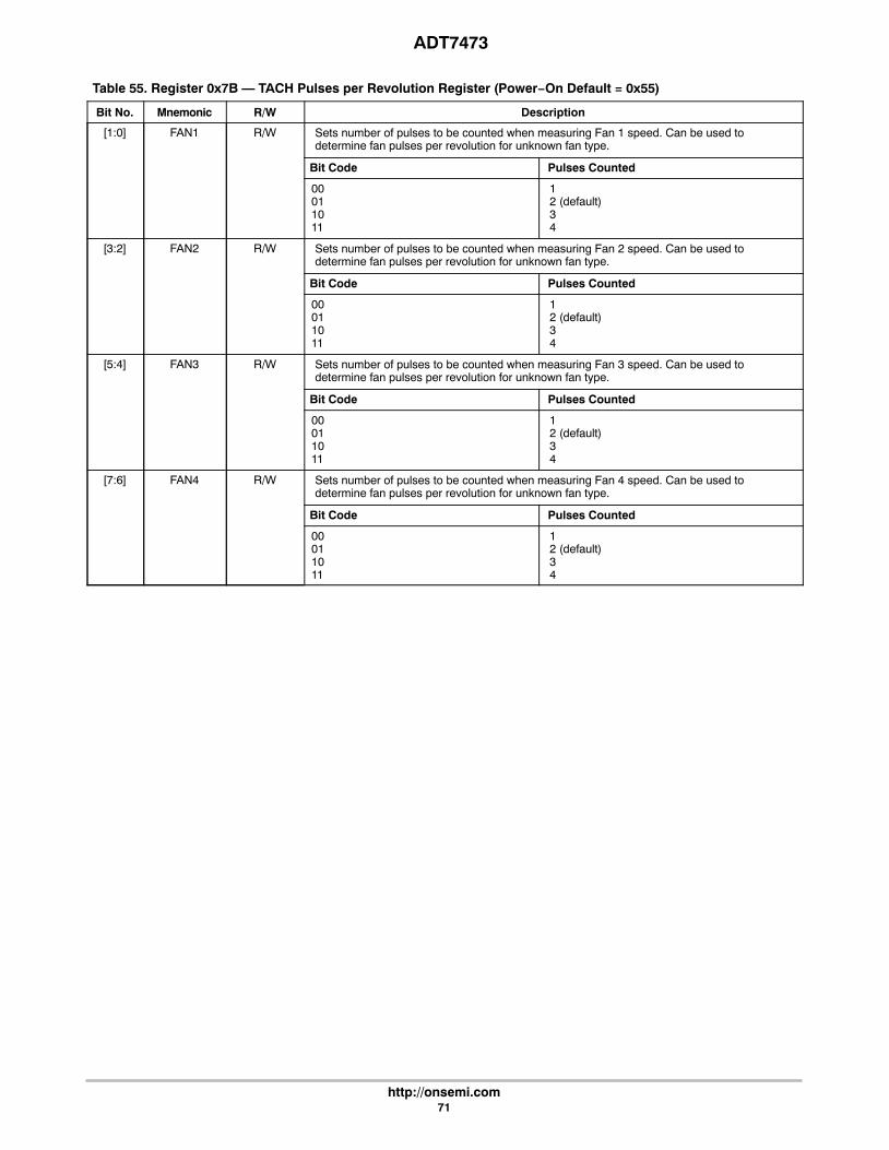
ADT7473
http://onsemi.com71
Table 55. Register 0x7B — TACH Pulses per Revolution Register (Power−On Default = 0x55)
Bit No. Mnemonic R/W Description
[1:0] FAN1 R/W Sets number of pulses to be counted when measuring Fan 1 speed. Can be used todetermine fan pulses per revolution for unknown fan type.
Bit Code Pulses Counted
00011011
12 (default)34
[3:2] FAN2 R/W Sets number of pulses to be counted when measuring Fan 2 speed. Can be used todetermine fan pulses per revolution for unknown fan type.
Bit Code Pulses Counted
00011011
12 (default)34
[5:4] FAN3 R/W Sets number of pulses to be counted when measuring Fan 3 speed. Can be used todetermine fan pulses per revolution for unknown fan type.
Bit Code Pulses Counted
00011011
12 (default)34
[7:6] FAN4 R/W Sets number of pulses to be counted when measuring Fan 4 speed. Can be used todetermine fan pulses per revolution for unknown fan type.
Bit Code Pulses Counted
00011011
12 (default)34
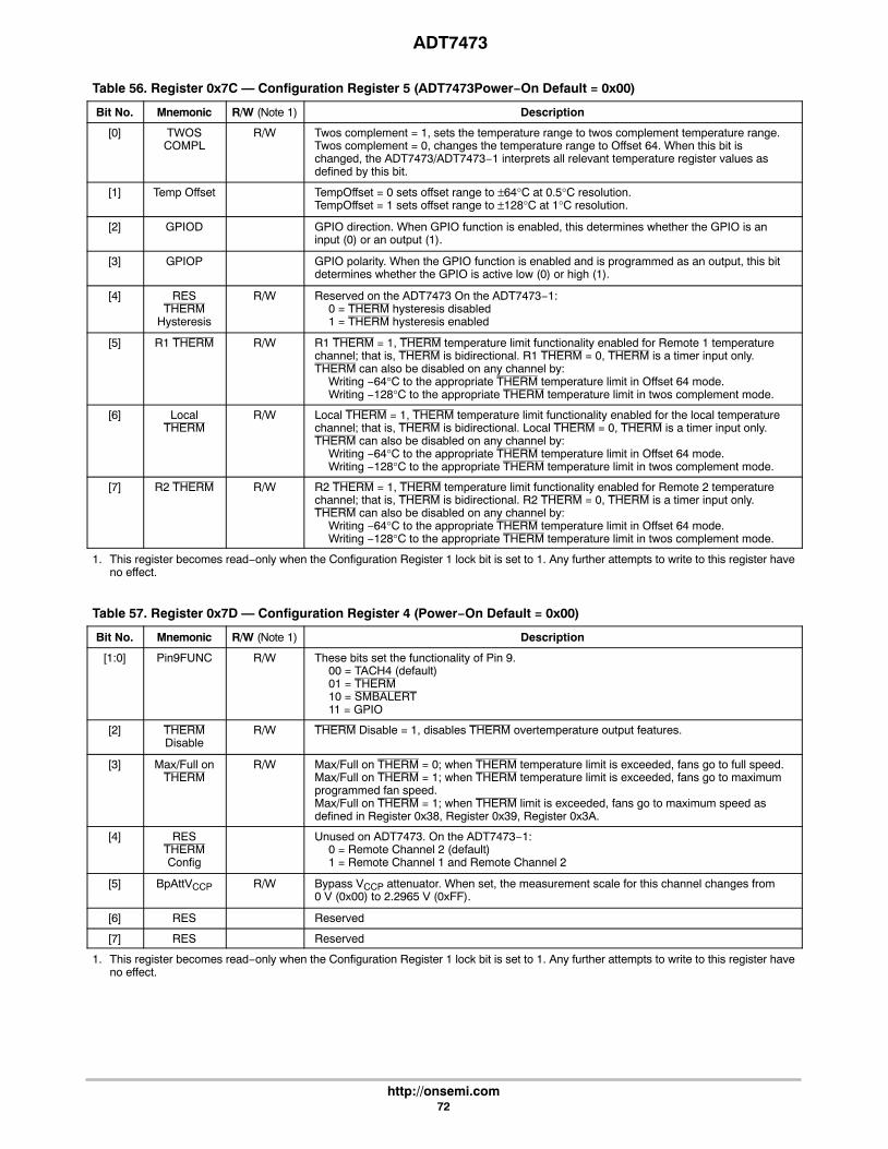
ADT7473
http://onsemi.com72
Table 56. Register 0x7C — Configuration Register 5 (ADT7473Power−On Default = 0x00)
Bit No. Mnemonic R/W (Note 1) Description
[0] TWOSCOMPL
R/W Twos complement = 1, sets the temperature range to twos complement temperature range.Twos complement = 0, changes the temperature range to Offset 64. When this bit ischanged, the ADT7473/ADT7473−1 interprets all relevant temperature register values asdefined by this bit.
[1] Temp Offset TempOffset = 0 sets offset range to ±64°C at 0.5°C resolution.TempOffset = 1 sets offset range to ±128°C at 1°C resolution.
[2] GPIOD GPIO direction. When GPIO function is enabled, this determines whether the GPIO is aninput (0) or an output (1).
[3] GPIOP GPIO polarity. When the GPIO function is enabled and is programmed as an output, this bitdetermines whether the GPIO is active low (0) or high (1).
[4] RESTHERM
Hysteresis
R/W Reserved on the ADT7473 On the ADT7473−1:0 = THERM hysteresis disabled1 = THERM hysteresis enabled
[5] R1 THERM R/W R1 THERM = 1, THERM temperature limit functionality enabled for Remote 1 temperaturechannel; that is, THERM is bidirectional. R1 THERM = 0, THERM is a timer input only.THERM can also be disabled on any channel by:
Writing −64°C to the appropriate THERM temperature limit in Offset 64 mode.Writing −128°C to the appropriate THERM temperature limit in twos complement mode.
[6] LocalTHERM
R/W Local THERM = 1, THERM temperature limit functionality enabled for the local temperaturechannel; that is, THERM is bidirectional. Local THERM = 0, THERM is a timer input only.THERM can also be disabled on any channel by:
Writing −64°C to the appropriate THERM temperature limit in Offset 64 mode.Writing −128°C to the appropriate THERM temperature limit in twos complement mode.
[7] R2 THERM R/W R2 THERM = 1, THERM temperature limit functionality enabled for Remote 2 temperaturechannel; that is, THERM is bidirectional. R2 THERM = 0, THERM is a timer input only.THERM can also be disabled on any channel by:
Writing −64°C to the appropriate THERM temperature limit in Offset 64 mode.Writing −128°C to the appropriate THERM temperature limit in twos complement mode.
1. This register becomes read−only when the Configuration Register 1 lock bit is set to 1. Any further attempts to write to this register haveno effect.
Table 57. Register 0x7D — Configuration Register 4 (Power−On Default = 0x00)
Bit No. Mnemonic R/W (Note 1) Description
[1:0] Pin9FUNC R/W These bits set the functionality of Pin 9.00 = TACH4 (default)01 = THERM10 = SMBALERT11 = GPIO
[2] THERMDisable
R/W THERM Disable = 1, disables THERM overtemperature output features.
[3] Max/Full onTHERM
R/W Max/Full on THERM = 0; when THERM temperature limit is exceeded, fans go to full speed.Max/Full on THERM = 1; when THERM temperature limit is exceeded, fans go to maximumprogrammed fan speed.Max/Full on THERM = 1; when THERM limit is exceeded, fans go to maximum speed asdefined in Register 0x38, Register 0x39, Register 0x3A.
[4] RESTHERMConfig
Unused on ADT7473. On the ADT7473−1:0 = Remote Channel 2 (default)1 = Remote Channel 1 and Remote Channel 2
[5] BpAttVCCP R/W Bypass VCCP attenuator. When set, the measurement scale for this channel changes from0 V (0x00) to 2.2965 V (0xFF).
[6] RES Reserved
[7] RES Reserved
1. This register becomes read−only when the Configuration Register 1 lock bit is set to 1. Any further attempts to write to this register haveno effect.

ADT7473
http://onsemi.com73
Table 58. Register 0x7E — Manufacturer’s Test Register 1 (Power−On Default = 0x00)
Bit No. Mnemonic R/W Description
[7:0] Reserved Read−only Manufacturer’s test register. These bits are reserved for manufacturer’s test purposes andshould not be written to under normal operation.
Table 59. Register 0x7F — Manufacturer’s Test Register 2 (Power−On Default = 0x00)
Bit No. Mnemonic R/W Description
[7:0] Reserved Read−only Manufacturer’s test register. These bits are reserved for manufacturer’s test purposes andshould not be written to under normal operation.
Table 60. Register 0x80 — Manufacturer’s Test Register 3 (Power−On Default = 0x10)
Bit No. Mnemonic R/W Description
[7:0] Reserved Read−only Manufacturer’s test register. These bits are reserved for manufacturer’s test purposes andshould not be written to under normal operation.
ORDERING INFORMATION
Device Order Number* Package Type Package Option Shipping†
ADT7473ARQZ
16−Lead QSOP RQ−16
98 Tube
ADT7473ARQZ−REEL 2500 Tape & Reel
ADT7473ARQZ−RL7 1000 Tape & Reel
ADT7473ARQZ−001 98 Tube
ADT7473ARQZ−1RL 2500 Tape & Reel
ADT7473ARQZ−1R7 1000 Tape & Reel
†For information on tape and reel specifications, including part orientation and tape sizes, please refer to our Tape and Reel PackagingSpecifications Brochure, BRD8011/D.
*These are Pb−Free packages.

ADT7473
http://onsemi.com74
PACKAGE DIMENSIONS
QSOP16CASE 492−01
ISSUE O
MAXMILLIMETERS
G
R
−B−
−A−
LM0.25 (0.010) T
U
−T−SEATINGPLANE
K
D16 PL
C
M0.25 (0.010) T B AS S
VN
JM
F
8 PL
DETAIL E
DETAIL E
H x 45
RAD.
MOLD PIN
DIM MINMAXMININCHES
A 4.80 4.980.189 0.196B 3.81 3.990.150 0.157C 1.55 1.730.061 0.068D 0.20 0.310.008 0.012F 0.41 0.890.016 0.035G 0.64 BSC0.025 BSCH 0.20 0.460.008 0.018J 0.249 0.1910.0098 0.0075K 0.10 0.250.004 0.010L 5.84 6.200.230 0.244M 0 8 0
8
N 0 7 0 7 P 0.18 0.280.007 0.011Q 0.51 DIA0.020 DIAR 0.64 0.890.025 0.035U 0.64 0.890.025 0.035V
NOTES:1. DIMENSIONING AND TOLERANCING PER ANSI
Y14.5M, 1982.2. CONTROLLING DIMENSION: INCH.3. THE BOTTOM PACKAGE SHALL BE BIGGER THAN
THE TOP PACKAGE BY 4 MILS (NOTE: LEAD SIDEONLY). BOTTOM PACKAGE DIMENSION SHALLFOLLOW THE DIMENSION STATED IN THISDRAWING.
4. PLASTIC DIMENSIONS DOES NOT INCLUDE MOLDFLASH OR PROTRUSIONS. MOLD FLASH ORPROTRUSIONS SHALL NOT EXCEED 6 MILS PERSIDE.
5. BOTTOM EJECTOR PIN WILL INCLUDE THECOUNTRY OF ORIGIN (COO) AND MOLD CAVITY I.D.
0 8 0
8
MARK
Q
P
0.013 X 0.005DP. MAX
RAD.0.005−0.010
TYP
ON Semiconductor and are registered trademarks of Semiconductor Components Industries, LLC (SCILLC). SCILLC reserves the right to make changes without further noticeto any products herein. SCILLC makes no warranty, representation or guarantee regarding the suitability of its products for any particular purpose, nor does SCILLC assume any liabilityarising out of the application or use of any product or circuit, and specifically disclaims any and all liability, including without limitation special, consequential or incidental damages.“Typical” parameters which may be provided in SCILLC data sheets and/or specifications can and do vary in different applications and actual performance may vary over time. Alloperating parameters, including “Typicals” must be validated for each customer application by customer’s technical experts. SCILLC does not convey any license under its patent rightsnor the rights of others. SCILLC products are not designed, intended, or authorized for use as components in systems intended for surgical implant into the body, or other applicationsintended to support or sustain life, or for any other application in which the failure of the SCILLC product could create a situation where personal injury or death may occur. ShouldBuyer purchase or use SCILLC products for any such unintended or unauthorized application, Buyer shall indemnify and hold SCILLC and its officers, employees, subsidiaries, affiliates,and distributors harmless against all claims, costs, damages, and expenses, and reasonable attorney fees arising out of, directly or indirectly, any claim of personal injury or deathassociated with such unintended or unauthorized use, even if such claim alleges that SCILLC was negligent regarding the design or manufacture of the part. SCILLC is an EqualOpportunity/Affirmative Action Employer. This literature is subject to all applicable copyright laws and is not for resale in any manner.
PUBLICATION ORDERING INFORMATIONN. American Technical Support: 800−282−9855 Toll FreeUSA/Canada
Europe, Middle East and Africa Technical Support:Phone: 421 33 790 2910
Japan Customer Focus CenterPhone: 81−3−5773−3850
ADT7473/D
dBCOOL is a registered trademarks of Semiconductor Components Industries, LLC (SCILLC). Pentium is a registered trademark of Intel Corporation.
LITERATURE FULFILLMENT:Literature Distribution Center for ON SemiconductorP.O. Box 5163, Denver, Colorado 80217 USAPhone: 303−675−2175 or 800−344−3860 Toll Free USA/CanadaFax: 303−675−2176 or 800−344−3867 Toll Free USA/CanadaEmail: [email protected]
ON Semiconductor Website: www.onsemi.com
Order Literature: http://www.onsemi.com/orderlit
For additional information, please contact your localSales Representative