adaptive memory power management techniques for hpc workloads
TRANSCRIPT

Adaptive Memory Power Management Techniques
for HPC Workloads
Karthik Elangovan, Ivan Rodero, Manish Parashar
Center for Autonomic Computing
Rutgers University, Piscataway NJ, USA
{elankart, irodero, parashar}@cac.rutgers.edu
Francesc Guim, Isaac Hernandez
Intel Barcelona
Barcelona, Spain
{francesc.guim, isaac.l.hernandez}@intel.com
Abstract—The memory subsystem is responsible for a largefraction of the energy consumed by compute nodes in HighPerformance Computing (HPC) systems. The rapid increase inthe number of cores has been accompanied by a correspondingincrease in the DRAM capacity and bandwidth, and as aresult, the memory system consumes a significant amount ofthe power budget available to a compute node. Consequently,there is a broad research effort focused on power managementtechniques using DRAM low-power modes. However, memorypower management continues to present many challenges.
In this paper, we study the potential of Dynamic Voltageand Frequency Scaling (DVFS) of the memory subsystems, andconsider the ability to select different frequencies for differentmemory channels. Our approach is based on tuning voltage andfrequency dynamically to maximize the energy savings whilemaintaining performance degradation within tolerable limits. Weassume that HPC applications do not demand maximum band-width throughout the entire period of execution. We can use theselow memory demand intervals to tune down the frequency and,as a result, applications can tolerate a reduction in bandwidth tosave energy. In this paper, we study application channel accesspatterns, and use these patterns to determine potential additionalenergy savings that can be achieved by accordingly controllingthe channels independently. We then evaluate the proposed DVFSalgorithm using a novel hybrid evaluation methodology thatincludes simulation as well as executions on real hardware. Ourresults demonstrate the large potential of adaptive memory powermanagement techniques based on DVFS for HPC workloads.
I. INTRODUCTION
High Performance Computing (HPC) have evolved over the
past decades into increasingly complex and powerful systems.
The power demand of high-end HPC systems is increasing
eight-fold every year [1]. Current HPC systems consume
several MWs of power, enough to power small towns, and
are in fact soon approaching the limits of the power available
to them. The costs of power for these high end HPC systems
runs into millions of dollars per year. As a result, improving
energy efficiency can reduce the total cost of ownership (TCO)
of HPC systems. since reducing energy consumption not only
reduces energy costs but also reduced costs for cooling and
other packaging infrastructure.
The memory subsystem is responsible for a large fraction
of the energy consumed by compute nodes in HPC systems.
Barrosso et al. [2] indicate that over the years the CPU has
evolved to an extent where it accounts for only 50% of
energy consumption. As a result, reducing energy consumption
through intelligent control of all subsystems [3] is critical. The
rapid increase in the number of cores has been accompanied by
a corresponding increase in DRAM capacity and bandwidth.
The memory system thus consumes a significant amount of
the power budget available to a compute node, and therefore
the design of novel memory power management techniques
has become crucial.
Research efforts on the power management of the memory
subsystem have revealed that (1) DRAMs have multiple low-
power states, but only a very coarse level of power control, (2)
exploiting these low power states is difficult primarily because
of the latency associated with switching to/from low-power
modes, (3) throttling can reduce energy consumption, and (4)
architectural changes can take time to seep into the market and
only provided there are no negative impact on yield. However,
current memory power control methods have many limitations
and there is still lot of space for new both DRAM architectural
and software control approaches.
In this paper, we consider the ability to select different
frequencies for different memory channels and propose to
selectively lower the frequency of the main memory using
DVFS to reduce energy consumption. Our overall goal is
to tune voltage and frequency dynamically to maximize the
energy savings while maintaining performance degradation
within tolerable limits. HPC workloads typically exhibit good
locality, which enables Last Level Cache (LLC) to capture
most of the accesses to the main memory. Therefore we
can assume that HPC applications may not require maximum
bandwidth all the time and that the bandwidth demand of these
applications is different on the different memory channels.
As a result, the applications can tolerate some bandwidth
reduction in order to save energy. This research is motivated
by three observations: (1) reducing frequency and voltage
reduces power considerably, (2) the time required to perform
read and write operations are not significantly affected by
change in frequency, and (3) the iterative pattern exhibited
by most scientific application allows tuning voltage and fre-
quency dynamically based on access patterns. Furthermore, we
build on the fact that recent processors designs incorporates
multiple on-chip memory controllers and multiple channels for
parallelism, and specifically, that a channel can be monitored
and, operated at appropriate voltage and frequency levels
corresponding to application usage patterns. To maintain the
978-1-4577-1950-9/11/$26.00 ©2011 IEEE

performance degradation within limits, we proposed a control
algorithm that, while evaluating the potential savings due to
DVFS prevents selecting frequencies that lead to significant
performance loss.
We evaluate the proposed DVFS algorithm using a novel
hybrid evaluation methodology that includes simulation as
well as executions on real hardware. We first study the applica-
tions channel access patterns, and then evaluate three possible
frequency selection strategies and two different algorithms for
mapping physical memory addresses to channels. The evalu-
ation is based on Intel Nehalem technology and demonstrates
the large potential of DVFS on memory utilization for HPC
workloads. Specifically, for the NAS Parallel Benchmarks,
the proposed control techniques provide around 55% memory
energy savings on average with only around 5% degradation
of execution time on average. We also observe that controlling
the channels independently provides considerable savings as
compared to controlling the frequency of all the channels
together, when applications exhibit uneven load.
The main contributions of this paper are summarized as
follows: (1) the study of memory access patterns, bandwidth
and channel usage for HPC workloads, (2) the design of a con-
trol algorithm for adaptive memory power management, (3) a
novel hybrid evaluation methodology that includes simulation
and executions on real hardware, and (4) an evaluation of the
proposed strategy on modern technology using different con-
figurations including number of memory channels, frequency
selection strategies, and physical address to channels mapping.
The rest of the paper is organized as follows. In Section
II, we review DRAM memories. In Section III, we discuss
related work. In Section IV, we describe our adaptive strategy
for memory power management. In Sections V and VI, we
present the evaluation methodology and the results obtained,
respectively. Finally, in Section VII, we conclude the paper
and outline directions for future work.
II. DRAM BACKGROUND
A. Memory System Organization
Data in a DRAM device has an array structure with multiple
rows and columns. The intersection of a row and column is a
storage cell, which is periodically refreshed because of gradual
data discharge. A row and column address can fetch only a
single bit from a single device in the array. Usually a number
of arrays are operated in parallel on each access. DRAM arrays
that act in unison on a request belong to the same bank, for
instance in a x4 DRAM four arrays act in parallel on each
access. The notation also indicates the column width (e.g., x8,
x16, x32 and x64 devices are commercially available). Figure
1 shows DRAM arrays grouped together.
Due to the DRAM organization the physical addresses
generated by applications cannot be used to directly access
DRAM, instead processors interface with DRAM through
memory controller which relieves the socket modules from
directly interfacing the DRAM. The memory controller has
to convert the physical addresses to a set of commands that
DRAM device understands. Physical addresses are split by the
On chip
Memory
Controller
DR
AM
DR
AM
DR
AM
DR
AM
Bank
DIMM
Rank
Device
Fig. 1. DRAM subsystem with DRAM modules (left) and DIMM organiza-tion with individual rank, bank and arrays inside each bank (right)
memory controller to identify a bank, then a row and column
within a bank.
Every DRAM operation (read/write) begins with an activate
command, which requires selecting a row with an appropriate
row address. The content of the entire row is transferred to the
sense amplifiers. Every bank has separate sense amplifiers and
each bank can be activated independently. Once the entire row
has been read it is said to be open and the bank is said to be
active. The next step is to select a column and then the content
of the column is placed on the data bus. DDRx SDRAMs
transfer data on both edges of the clock cycle. The final step is
to restore the data back to the cells with a pre-charge operation
that closes a row. The set of commands described previously
can be pipelined when accessing different banks in sequence,
and modern memory controllers exploit this to increase the
bandwidth.
The memory controller can close the row after a read/write
access with a pre-charge command. In closed page DRAMs,
rows are immediately closed after a row access command,
while in open page DRAMs, rows remain opened expecting
subsequent hits to the same row. In this study we evaluate only
closed page RAMs.
B. DRAM timing
The basic timing parameters for generic DRAM commands
that will be used throughout this paper are the following:
• tRCD : Time to move an entire row of data to the sense
amplifiers.
• tCAS : Time interval between column read command and
availability of data in the data bus.
• tCWL: Time interval between column write command
and availability of data in the data bus.
• tRAS : Time interval between row access and data restora-
tion back to the cells.
• tRP : Time taken to pre-charge a row.
• tRC : Minimum time interval that has to elapse between
different accesses to same row in a bank.
• tWR: Time to restore the write data from sense amplifiers
back to the cells.
Every read operation includes row activation (tRCD), col-
umn read (tCAS), data out (tBURST ) and pre-charge (tRP ).

The total time is tRCD + tCAS + tBURST + tRP . DDR3
devices can perform each of these operations in 10ns. The
timing parameters for the write operation are the same, except
the column access takes tCWL, and there is an additional tWR
waiting period to the end of the last data into sense amplifiers.
C. Voltage and Frequency Scaling
The JEDEC memory standards [4] are the specifications for
semiconductor memory circuits and similar storage devices
adopted by the JEDEC Solid State Technology Association.
They allow changing the input memory frequency, but the
transition should respect the timing parameters specified by
the standard; however, commercially available DRAM devices
do not support multiple voltage domains. In this paper, we
assume the DRAM to operate properly within the voltage
levels configurable using the BIOS settings. Table I lists
the voltage and frequency combinations considered in this
study for DDR3 SDRAM along with the power breakup of a
2GB DIMM (256x64) - calculated using power model in [5].
Note that the voltage range [1.575V–1.425V] is the allowable
voltage range of the power supply.
III. RELATED WORK
Over the last years, processors have evolved to become
energy efficient supporting multiple operating modes. At a
very coarse level, power management at the system level
consisted on monitoring the system load and shutting down
unused clusters or transitioning unused nodes to low power
modes [6]. Such algorithms are based on the availability of suf-
ficient idle periods and propose to batch work [6] to increase
the probability of such idle periods. Computing nodes incur
latency only when they exit from these low-power modes.
Other studies [7], [8], [9], [10] have proven that dynamically
varying the voltage and frequency proportional to system load
is effective in reducing energy consumption. DVFS provides
power savings at the cost of a small increase in execution time.
Other approaches conducted on power management techniques
are focused at the processor level, for example, Cai et al.
[11] propose a DVFS techniques based on the hardware thread
runtime characterization.
The previous approaches tackled the energy consumption
optimizations focused in the computing elements. Memory
devices, which were once considered to be undesirable candi-
dates for power consumption, began to significantly contribute
to overall system energy consumption. Just like processors,
DRAM devices have several low power modes. Delaluz et
al. [12] present software and hardware assisted methods for
memory power management. They studied compiler-directed
techniques [13], [12] , as well as OS-based approaches [14],
[15] to determine idle periods for transitioning devices to low-
power modes. Even though this approach is very conservative,
switching to/from low-power modes during unwanted periods
can be prevented; however it is not very effective on multi-core
systems. Cho et al. [16] studied assigning CPU frequencies
for DVFS that is memory-aware, because focus of all prior
work was on optimal assignment of frequencies to CPU, thus
ignoring memory. Huang et al. [17] proposed a power-aware
virtual memory implementation in the OS to reduce memory
energy consumption. Fradj et al. [18], [19] propose multi-
banking techniques that consist of setting individually banks
in lower power modes when they are not accessed.
Self-Monitoring [12] approach can be effective with a
control algorithm to chose between power modes for memory
devices. The key is to determine idle periods to transition
devices to low-power modes; however, self-monitoring control
algorithms are threshold-based, therefore, an algorithm that
transitions into low-power modes too frequently can increase
latency, while a very sluggish algorithm can miss out on
opportunities to save power. Li et al. [20], [21], [22] proposed
a self-tuning energy management algorithm to provide perfor-
mance guarantees. The algorithm tunes threshold parameters
at different points of execution. Diniz et al. [23] studied
dynamic approaches for limiting the power consumption of
main memory by limiting consumption and adjusting the
power states of the memory devices, as a function of the
memory load. Hur et al. [24] took an entire different approach
towards DRAM power management. DRAM commands are
delayed in memory controller to increase idle periods, and to
exploit low-power modes of DRAMs. Commands are delayed
in memory controller for a certain number of cycles which is
determined by a delay estimator.
Several architectural changes have also been proposed. Rank
subsetting [25] and Mini-Rank [26] tackle energy consumption
constraint by dividing a rank into subsets. This approach
reduces the number of chips which are put to work at each
memory access. Udipi et al. [27] suggested changes to internal
organization of DRAM devices. The authors argue that an
open-paged policy does not present any improvements for a
multi-core architecture because an opened row has one or two
hits on average. Building on that argument it is unnecessary
to read all the bits to the sense amplifiers, thus reducing
the number of bits that are touched can decrease the energy
consumption.
Deng et al. [28] proposed dynamic frequency scaling of
the main memory. The frequency of all memory channels is
changed to provide energy savings with guaranteed perfor-
mance degradation. David et al. [29] proposed and imple-
mented DVFS on actual hardware. Their control algorithm
monitors the bandwidth and dynamically varies the voltage
and frequency. Both concurrent research effort was focused
on performing DVFS on all the channels simultaneously while
the focus of our study has been clearly on evaluating the
potential of controlling the voltage and frequency of each
channel independently.
IV. ADAPTIVE MEMORY POWER MANAGEMENT
Our work has been primarily motivated by two characteris-
tics of the applications’ behavior: (1) bandwidth demand, and
(2) the memory access patterns. As mentioned previously, ap-
plications rarely demand peak bandwidth from main memory
since on chip caches work efficiently for capturing accesses to
main memory. LLC misses of an application can be used to

Frequency Voltage Pds(PRE STBY) Pds(ACT STBY) Pds(ACT) Pds(WR) Pds(RD) Pdq(RD) Pdq(WR)
(MHz) (V) (mW) (mW) (mW) (mW) (mW) (mW) (mW)
933 1.5750 252 466 226 919 793 96 620
800 1.5375 240 420 170 660 720 91 591
667 1.5000 229 400 104 457 514 87 562
533 1.4625 184 326 91 380 435 83 535
400 1.4250 131 232 65 271 310 79 508
TABLE IFREQUENCY AND VOLTAGE LEVELS AND POWER BREAKUP OF A 2GB DIMM (256MX64) FROM [5]
0 100 200 300 400 500 600 700 800 900 10000
10
20
30
40
50
Instructions(billions)
Mis
ses p
er
1000 instr
uctions
0 50 100 150 200 250 300 350 4000
5
10
15
20
25
Instructions(billions)
Mis
ses p
er
1000 instr
uctions
Fig. 2. MPKI of NAS BT(top) and NAS FT (bottom)
derive bandwidth demand since it has positive correlation with
bandwidth. Figure 2 shows misses access, expressed as Misses
Per Kilo Instructions (MPKI) of two NAS benchmarks that
were collected using CMPSim as described in Section V, and
demonstrate the time varying behavior of both applications.
There are periods of high and low bandwidth demand, and
switching to a lower voltage and frequency during these
low bandwidth demand periods, applications will not suffer
significantly.
A. Channel Mappings from Physical Address
As described previously the processor cannot directly access
DRAM devices. The physical address is sent to the memory
controller which splits the address to first find the physical
channel, then the rank, and then the bank within a rank. The
process of identifying the channel number is proprietary to
each memory controller design, for instance, considering the
example shown in Figure 3 the physical address is divided to
address different parts of the device, and the Row ID is mapped
to the most significant bits so that subsequent addresses go
to the same row. We consider two different algorithms for
mapping memory physical addresses to channels:
• Default: Accesses are clustered to certain channels thus
reducing activity on other channels. This allows us to tune
Physical Address
31 30 29 28 27 26 25 24 23 22 21 20 19 18 17 16 15 14 13 12 11 10 9 8 7
Row
Bank
Col ID
Chan ID
Fig. 3. Channel mapping example
down the voltage and frequency of channels which are
relatively lightly loaded. For instance, with 4GB Physical
memory having 8 channels. Each channel can be used to
address 512MB of memory. If the Most Significant Bits
are used the resolve the channel address then accesses
to first 512MB will go to the first channel, accesses to
second 512MB will go to the second channel and so on.
• Interleaving: Load can be distributed across different
channels if subsequent cache lines are mapped to different
channels. This can be achieved by using Least Significant
Bits of the physical address to resolve the channel num-
ber.
Figures 4 and 5 illustrate how the algorithm for mapping
physical memory addressed to channels can significantly affect
the memory access pattern, and presumable the application
behavior.
B. Memory Access Patterns
Memory access patterns of three NAS Benchmarks were
collected using mptrace and CMPSim (see Section V). CMP-
Sim dumps processor specific information whenever a hard-
ware thread hits 109 instructions. Mptrace is used to obtain
the physical addresses accessed. The data is then processed
to obtain the channels access patterns using different channel
mapping algorithms. Figures 4 and 5 show the memory access
patterns for four, eight and sixteen channels. Access patterns
were collected for different regions (i.e., a block of instruc-
tions) of the application. The exact number of application
instructions for a region is not fixed, and varies with the
CMPSim output dump frequency (i.e., when a thread hits 109
instructions). The memory access patterns exhibited by appli-
cations motivate the use of the adaptive techniques proposed
in this work. Peak bandwidth is not always demanded by ap-
plications and there is unequal distribution of accesses across
channels. This asymmetry presents opportunities to control the
channels independently. The plots show that there is equal

12
34
0
5
10
15
20
25
30
0
5
10
15
20
25
30
35
Program Region
Channels
Perc
enta
ge o
f channel access
1 2 3 4 5 6 7 8
0
5
10
15
20
25
30
0
5
10
15
20
25
Program Region
ChannelsP
erc
en
tag
e o
f ch
an
ne
l a
cce
ss
12
34
56
78
910
1112
1314
1516
0
5
10
15
20
25
30
0
5
10
15
20
Program Region
Channels
Pe
rce
nta
ge
of
ch
an
ne
l a
cce
ss
Fig. 4. Access pattern of NAS BT benchmark with 4 channels (left), 8 channels (center) and 16 channels (right) with Interleaving channel mapping algorithm
1 2 3 4
0
5
10
15
20
25
30
0
5
10
15
20
25
30
35
40
45
Program Region
Channels
Pe
rce
nta
ge
of
ch
an
ne
l a
cce
ss
1 2 3 4 5 6 7 8
0
5
10
15
20
25
30
0
5
10
15
20
25
Program Region
Channels
Pe
rce
nta
ge
of
ch
an
ne
l a
cce
ss
1 2 3 4 5 6 7 8 910111213141516
0
5
10
15
20
25
30
0
2
4
6
8
10
12
14
Program Region
Channels
Pe
rce
nta
ge
of
ch
an
ne
l a
cce
ss
Fig. 5. Access pattern of NAS BT benchmark with 4 channels (left), 8 channels (center) and 16 channels (right) with Default channel mapping algorithm
distribution of traffic with 4 channels; however, with 8 and 16
channels the benchmark exhibits affinity in accessing a cer-
tain group of channels. Dynamically changing the frequency
is not going to affect the performance of the applications
significantly. Additional observation of access patterns shows
that channels can be further tuned independently because of
unequal distribution of traffic.
C. Control Algorithm
The control algorithm selects the operating voltage and
frequency of main memory. It is invoked on certain points
along the execution of the program, and uses observed system
parameters during current phase of execution to obtain possible
energy savings attainable at different operating states. The
operating state here refers to voltage and frequency levels
of channels. The control algorithm uses the power model
described in SectionV-D. It is possible to compute the input
parameters of the power model from the execution time. How-
ever, to prevent the power control algorithm from calculating
this parameter, it is advisable to use a counter. In addition, the
hardware should also have counters for LLC misses and total
instruction executed. The counter for LLC misses should be
maintained on a per-channel basis.
To calculate the power dissipation at other frequency set-
tings the execution time at all the other frequencies should
be found. Execution time in total number of cycles (TNC)
is given by Eq. 1 where ICPU is the total non-memory
instructions, Imem is the total memory instructions, CPImem
is cycles per memory instructions that can be found using the
performance model (described in Section V-C. If the control
algorithm is invoked at fixed intervals TNC will be known
for the current state. CPICPU can be computed using Eq.
1. CPICPU is constant at all the other states since changing
frequency will not affect non-memory instructions.
TNC = (ICPU × CPICPU ) + (Imem × CPImem) (1)
The control algorithm performs the following sequence of
steps when it is invoked:
Step i: Read all the counters.

Step ii: Use the performance model to calculate the
execution time of the current phase at all the possible
voltage and frequency levels.
Step iii: Calculate the power consumed by the other
operating states.
Step iv: Calculate the energy savings for all the states,
i.e., savings compared to operating all the channels at
maximum frequency.
Step v: Choose a state for the next phase that maximizes
energy savings while keeping CPI degradation within a
specified limit.
With M possible operating frequencies and n channels we
can have Mn possible states. Since the complexity of the
control algorithm increases exponentially with the number
of channels, we have considered three possible frequency
selection strategies:
• Exhaustive Search: All the frequencies are considered in
this method (Mn possible states). The cost of executing
the control algorithm with this scheme becomes very high
with 8 and 16 channels.
• 3 Levels: Three frequency levels can be considered at
a time, for instance, if we start with 933MHz then
933MHz, 800MHz and 667MHz are considered for
the next phase. If 667MHz is selected for the next phase
then 800MHz, 667MHz and 533MHz are considered
for the next phase. With such a scheme the complexity
of the algorithm is reduced considerably.
• Ganged: The number of possible operating states can be
greatly reduced by slaving all the channels together, even
when all the five frequencies are considered, e.g., there
can be only 5 possible states.
V. EVALUATION METHODOLOGY
Since the actual implementation of DVFS is not available
for currently available hardware, the evaluation of the control
algorithm is performed using simulation. However, part of
input data of the control algorithm is obtained using tools that
run on the actual execution platform for which the simulator
is configured.
The CMPSim simulator is used to capture the time varying
behavior of the applications. The simulator was configured
to produce statistics when any hardware thread reaches 109
instructions. Since CMPSim can model the application be-
havior only until the LLC, mptrace is used to collect the
physical address traces of all the benchmarks. Results from
both CMPSim and mptrace are used as input by the control
algorithm along with a performance and a power model. The
performance model is used together with the LLC statistics
(CMPSim) and channel access ratios (mptrace) to find the
latency of read/write operations for all operating frequencies.
After obtaining the average latency for a given frequency
(fsys) from the performance model, the actual execution time
of the program at fsys can be computed using Eq. 2, where
Nc′ is the total execution time (in cycles) after compensating
for LLC misses, and Nc is the total execution time (in
cycles) produced by the simulator assuming that LLC misses
are penalized with a 350 cycle latency, which is a standard
technology parameter.
Nc′ = Nc − (350 × Misses) + (Latency × Misses) (2)
The execution time is then used to find the activity param-
eters that are computed for all possible operating states. Next,
the power model is used to obtain the power dissipation, and
the last step is selecting a state that provides maximum energy
savings within allowable CPI degradation limits.
A. CMPSim Simulator
CMPSim is a PIN [30][31] tool that intercepts memory
access operations that are fed to a Chip Multiprocessor (CMP)
cache simulator [32]. The model implements a detailed cache
hierarchy with DL1/IL1, UL2, UL3 and memory. The simu-
lator can be configured to model complex cache hierarchies,
e.g., a SMP machine with 32 cores sharing the L2 and L3. In
fact, the recent processor architectures can be modeled using
CMPSim.
CMPSim can capture cache behavior of single and multi-
threaded workloads. CMPSim can gather a wide variety of
statistics for an application, which are saved to an output file
periodically. The log file contains information about instruc-
tion profile, total number of cache accesses and misses at all
levels, and cache sharing between multiple threads, etc. Moses
et al. [33] present a very detailed study of CMPSim.
B. Mptrace
The Intel PIN project aims to provide dynamic instrumen-
tation techniques to gather information about the instructions
that applications execute. PIN API provides mechanisms to
implement callbacks that are called where specific events occur
on the execution of the target application (i.e., execution of
memory access operation).
Other tools that profile the the applications memory access
can be found in the PIN SDK. However, no PIN tool or
similar instrumentation tool has been provided to profile the
physical memory accesses that applications request. Mptrace
is a PIN-based tool that allows intercepting the processes
memory accesses, and translating the virtual addresses to
physical addresses. It uses the page map file [34] system to
translate the virtual address to physical address. The pagemap
file system was released with version 2.6.25 of the Linux
kernel and can be accessed through the /proc/pid/pagemap file.
As is described in the kernel source [34], this file allows a user
space process to find to which physical frame each virtual page
is mapped. It contains one 64-bit value for each virtual page,
containing the following data (from fs/proc/task mmu.c):
• Bits 0-54: page frame number (PFN) if present
• Bits 0-4: swap type if swapped
• Bits 5-54: swap offset if swapped
• Bits 55-60: page shift (page size = 1 page shift)
• Bit 61: reserved for future use
• Bit 62: page swapped
• Bit 63: page present

ServerBank 3
Bank 2
Bank 1
Bank m
mi
mi
mi
mi
mi
Fig. 6. Memory controller queueing model
Using the pagemap system, the mptrace PIN tools provides
several functionalities to characterize how the applications
access the physical memory pages. The format and information
required is highly customizable, it provides information related
to cache access (way and set), and memory accesses (physical
page address). It also provides ways to reduce the amount of
generated information, such as, sampling and trace disabling
when the application loads data, or the caches are warming up.
The current implementation of mptrace provides mechanisms
to characterize the memory accesses on the flight. Thus, this
PIN tool can provide summarized information about how an
application is using the main memory. For example, it pro-
vides page access histograms, or clusters of memory regions
accessed during an interval of time.
C. Performance Model
CMPSim assumes the main memory access latency of 350
cycles for both read and write operations. A memory access
(read/write) missing the LLC will incur the delays shown in
Eq. 3, where tr is the time for read access, tw is the time for
write access and td is the average queueing delay incurred by
a memory access. tr and tw include the time for a complete
data transfer from a DRAM device back to (or from) CPU.
An estimate of td is necessary to calculate the total delay as
described below.
Latency = tr + td (reads)
= tw + td (writes)(3)
The memory controller (see Figure 6) maintains one pro-
cessing queue per bank, and λi is the arrival rate of requests on
channel i (we assume that all the banks are equally accessed).
The traffic distributes into all the queues equally. The request
at the head of each queue is serviced on a round-Robin basis.
Time to service a request includes the complete access time
(for read and write operations.). Since we model a closed
page DRAM, a read access includes row activation (tRCD),
column access (tCL), data transfer (tBURST ) and a pre-charge
command to close the row (tRP ). The timing parameter for a
write operation is similar except that the column access takes
tCWL, and there is a tWR interval between tBURST and tRP .
tR (tW ) denotes the complete time interval required to perform
read (write) operation. The memory controller has a Poisson
arrival distribution, distributed service time, a single server
and m traffic streams. This is an M/G/1 queue with m users
polling for the server. The average waiting time of a request in
a queue (td) can now be estimated, and can be used to calculate
the latency. The probability mass function of service time of
a request is shown in Eqs. 4 – 7, where pR and pW represents
the probability that an access is read and write, respectively,
and λ, pR and pW can be calculated from data collected from
CMPSim and mptrace. Since we assume equal bank access,
the waiting time of a request in the queue is given by waiting
time of a M/G/1 queue.
fS(s) =
{
pR, s = tRpW , s = tW
(4)
S = E{S} =1
µ(5)
S2 = E{S2} (6)
td =λS2
2(1 − ρ)(7)
CMPSim outputs instructions executed and LLC misses on
a per thread basis. This can be used to calculate the average
interval between any two LLC misses as shown in Eqs. 8 and
9, where we τ is the average gap between any two LLC misses,
αkj is the fraction of accesses from thread k going to channel
j. Parameter λ can be used to calculate average waiting time
of a request to channel j, and td can be used to correct the
total number of cycles elapsed.
τ =Instructions Executed
LLC Misses×
×Cycles − (350 × LLC Misses)
(Instructions Executed − LLC Misses)×
1
fCPU
(8)
λj =α1j
τ1
+α2j
τ2
+ · · · +αkj
τk
(9)
D. Power Model
In our simulations we have calculated active power (PACT ),
background power (PACT STBY and PPRE STBY ), read and
write power (PRD and PWR) and termination power(Pterm)
according to the model for memory power described in [5].
The specific parameters required by the DRAM power model
are listed below.
• BNK PRE Percentage of cycles that DRAM spent in
pre-charge mode.
• RD Sch Percentage of DRAM cycles that were out-
putting read data.
• WR Sch Percentage of DRAM cycles that were out-
putting write data.
BNK PRE is used to compute background power while
RD Sch and WR Sch are used to compute read, write and
termination power. These parameters are described in detail
in [5], and they can be computed using the performance
model after obtaining the average latency of read and write
operations. Eq. 10 computes the energy consumption, where
Pftotal represents the total power dissipation, and Texec the
execution time at frequency f .
Ef = Pftotal × Texec (10)

BT FT CG35
40
45
50
55%
En
erg
y S
avin
gs
Ganged
3 Levels
Exhaustive
BT FT CG0
0.5
1
1.5
2
2.5
% I
ncre
ase
in
Exe
cu
tio
n T
ime
Ganged
3 Levels
Exhaustive
BT FT CG35
40
45
50
55
60
% E
ne
rgy S
avin
gs
Ganged
3 Levels
Exhaustive
BT FT CG0
0.5
1
1.5
2
2.5
% I
ncre
ase
in
Exe
cu
tio
n T
ime
Ganged
3 Levels
Exhaustive
Fig. 7. Percentage energy savings and increase in execution time with 4 channels. Interleaving (left) and Default (right) mapping
BT FT CG35
40
45
50
55
60
% E
ne
rgy S
avin
gs
Ganged
3 Levels
BT FT CG0
2
4
6
8
10
% I
ncre
ase
in
Exe
cu
tio
n T
ime
Ganged
3 Levels
BT FT CG35
40
45
50
55
60
% E
ne
rgy S
avin
gs
Ganged
3 Levels
BT FT CG0
2
4
6
8
10
% I
ncre
ase
in
Exe
cu
tio
n T
ime
Ganged
3 Levels
Fig. 8. Percentage energy savings and increase in execution time with 8 channels. Interleaving (left) and Default (right) mapping
BT FT CG35
40
45
50
55
60
% E
ne
rgy S
avin
gs
Ganged
BT FT CG0
2
4
6
8
10
12
% I
ncre
ase
in
Exe
cu
tio
n T
ime
Ganged
BT FT CG35
40
45
50
55
60
% E
ne
rgy S
avin
gs
Ganged
BT FT CG0
2
4
6
8
10
12
% I
ncre
ase
in
Exe
cu
tio
n T
ime
Ganged
Fig. 9. Percentage energy savings and increase in execution time with 16 channels. Interleaving (left) and Default (right) mapping
VI. RESULTS
NAS Parallel Benchmarks were used to evaluate the po-
tential of adaptive DRAM power management. CMPSim was
used to collect statistics of benchmark execution for the
configuration in Table II and the power model described in [5].
Memory access patterns of benchmarks were obtained using
mptrace on actual hardware (same configuration as shown in
table II). We collected results for 4, 8 and 16 DDR3 channels
with 2GB of physical memory in each channel. Control
algorithm was configured to sacrifice up to 5% degradation
in CPI when choosing the next state. Energy savings and
increase in total execution time of the benchmarks for varying
number of channels, mapping algorithms and frequency selec-
tion methods are discussed in this section. Percentage increase
is calculated with respect to running the benchmark with all
the channels operated at maximum frequency. Energy savings
reported in this paper are savings in main memory and not
the system as a whole. Results show the potential of adaptive
memory power management to obtain significant savings with
5% degradation.
Figure 7 shows the energy savings and the increase in
the execution time obtained with a 4 channel DDR3 system
using three frequency selection strategies and two channel
mapping policies. Average energy savings for BT, FT and
CG benchmarks were 42.95%, 51.33% and 52.19%, and the
increase in execution time is lower than 2.5%. with all the three
benchmarks. Both the mapping algorithms display the same
trend with all the frequency selection methods. Investigating
Feature Specification
Cores 8 Cores, 2 HW threads per core, 2.4GHz
L1 Cache 32KB, 8-way set associative
L2 Cache 256KB, 16-way set associative 5cycles/hit
L3 Cache 16MB, 4-way set associative 15 cycles/hit
TABLE IICHARACTERISTICS OF THE SIMULATED ARCHITECTURE
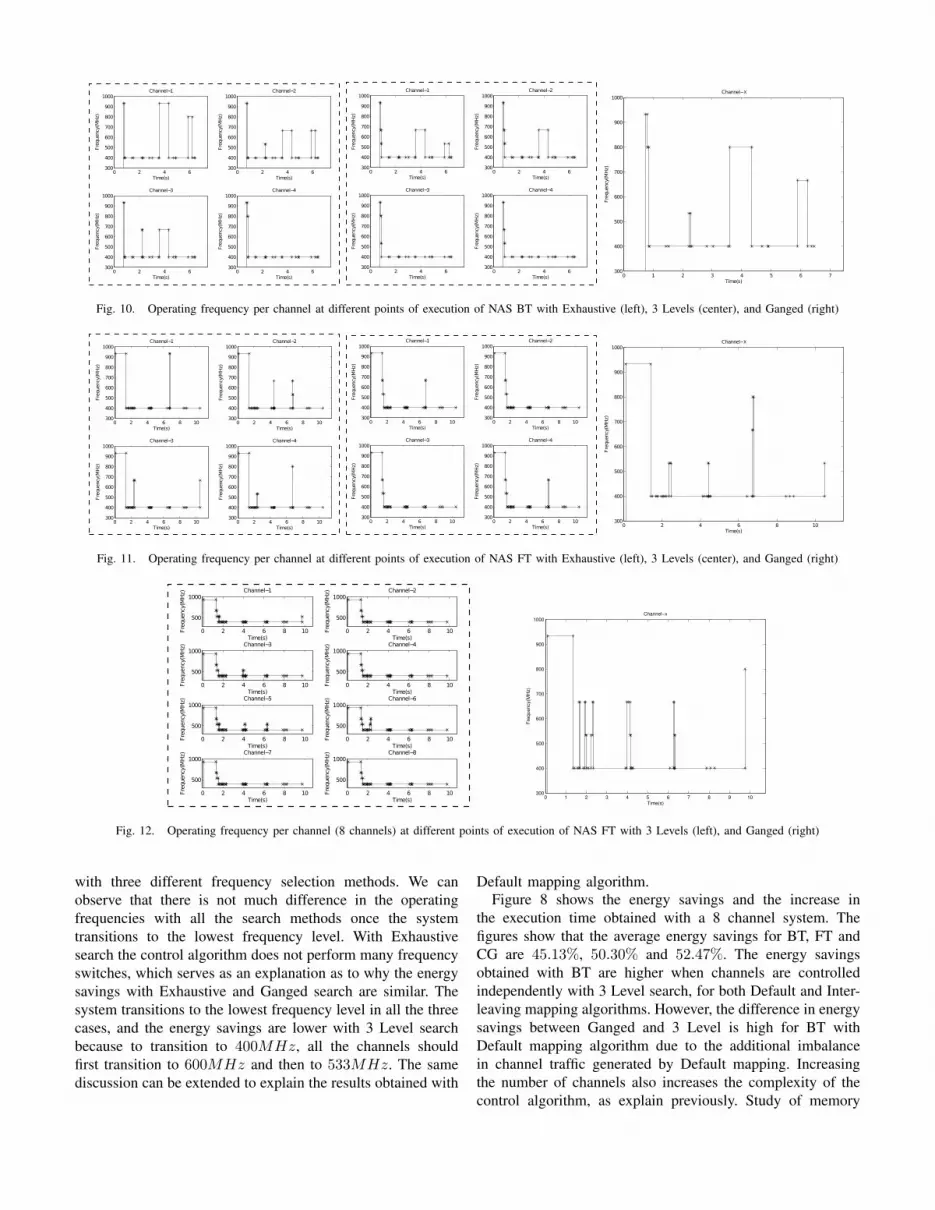
dynamic behavior of the benchmark will enable us to better
understand the results . Figures 10 and 11 show the dynamic
behavior of two NAS benchmarks. Energy savings with 3
Level search are higher than exhaustive frequency search for
BT. This can be explained by looking at Figure 10, operating
frequencies of the channels with exhaustive search are similar
to 3 level search except for the 900MHz switch which was
avoided by 3 Level search. Figure 7 also shows that with
Exhaustive search the increase in execution time is the lowest
with respect to the other policies. In both the cases the control
algorithm transitions the system to the lowest frequency that
is available and the channels are switched back to higher
frequencies only during periods of high bandwidth demand.
This behavior is conformant with our assumption that HPC
applications can sacrifice performance for savings in energy
because of existence of periods of high and low bandwidth
demands.
Figure 11 shows the channel operating frequencies for FT
0 2 4 6300
400
500
600
700
800
900
1000Channel−1
Time(s)
Frequency(M
Hz)
0 2 4 6300
400
500
600
700
800
900
1000Channel−2
Time(s)
Frequency(M
Hz)
0 2 4 6300
400
500
600
700
800
900
1000Channel−3
Time(s)
Frequency(M
Hz)
0 2 4 6300
400
500
600
700
800
900
1000Channel−4
Time(s)
Frequency(M
Hz)
0 2 4 6300
400
500
600
700
800
900
1000Channel−1
Time(s)
Frequency(M
Hz)
0 2 4 6300
400
500
600
700
800
900
1000Channel−2
Time(s)
Frequency(M
Hz)
0 2 4 6300
400
500
600
700
800
900
1000Channel−3
Time(s)
Frequency(M
Hz)
0 2 4 6300
400
500
600
700
800
900
1000Channel−4
Time(s)
Frequency(M
Hz)
0 1 2 3 4 5 6 7300
400
500
600
700
800
900
1000Channel−1
Time(s)
Frequency(M
Hz)
X
Fig. 10. Operating frequency per channel at different points of execution of NAS BT with Exhaustive (left), 3 Levels (center), and Ganged (right)
0 2 4 6 8 10300
400
500
600
700
800
900
1000Channel−1
Time(s)
Frequency(M
Hz)
0 2 4 6 8 10300
400
500
600
700
800
900
1000Channel−2
Time(s)
Frequency(M
Hz)
0 2 4 6 8 10300
400
500
600
700
800
900
1000Channel−3
Time(s)
Frequency(M
Hz)
0 2 4 6 8 10300
400
500
600
700
800
900
1000Channel−4
Time(s)
Frequency(M
Hz)
0 2 4 6 8 10300
400
500
600
700
800
900
1000Channel−1
Time(s)
Frequency(M
Hz)
X
Fig. 11. Operating frequency per channel at different points of execution of NAS FT with Exhaustive (left), 3 Levels (center), and Ganged (right)
0 2 4 6 8 10
500
1000Channel−1
Time(s)
Frequency(MHz)
0 2 4 6 8 10
500
1000Channel−2
Time(s)
Frequency(MHz)
0 2 4 6 8 10
500
1000Channel−3
Time(s)
Frequency(MHz)
0 2 4 6 8 10
500
1000Channel−4
Time(s)
Frequency(MHz)
0 2 4 6 8 10
500
1000Channel−5
Time(s)
Frequency(MHz)
0 2 4 6 8 10
500
1000Channel−6
Time(s)
Frequency(MHz)
0 2 4 6 8 10
500
1000Channel−7
Time(s)
Frequency(MHz)
0 2 4 6 8 10
500
1000Channel−8
Time(s)
Frequency(MHz)
0 1 2 3 4 5 6 7 8 9 10300
400
500
600
700
800
900
1000Channel−x
Time(s)
Fre
quency(M
Hz)
Fig. 12. Operating frequency per channel (8 channels) at different points of execution of NAS FT with 3 Levels (left), and Ganged (right)
with three different frequency selection methods. We can
observe that there is not much difference in the operating
frequencies with all the search methods once the system
transitions to the lowest frequency level. With Exhaustive
search the control algorithm does not perform many frequency
switches, which serves as an explanation as to why the energy
savings with Exhaustive and Ganged search are similar. The
system transitions to the lowest frequency level in all the three
cases, and the energy savings are lower with 3 Level search
because to transition to 400MHz, all the channels should
first transition to 600MHz and then to 533MHz. The same
discussion can be extended to explain the results obtained with
Default mapping algorithm.
Figure 8 shows the energy savings and the increase in
the execution time obtained with a 8 channel system. The
figures show that the average energy savings for BT, FT and
CG are 45.13%, 50.30% and 52.47%. The energy savings
obtained with BT are higher when channels are controlled
independently with 3 Level search, for both Default and Inter-
leaving mapping algorithms. However, the difference in energy
savings between Ganged and 3 Level is high for BT with
Default mapping algorithm due to the additional imbalance
in channel traffic generated by Default mapping. Increasing
the number of channels also increases the complexity of the
control algorithm, as explain previously. Study of memory

access patterns showed increase in imbalance among channels
when the number of channels is increased. This presents the
control algorithm with even fine grained control. Controlling
the channels independently can present more opportunities to
save energy since channels that have very low traffic can
be operated at the lowest frequency, while the frequency of
loaded channels can be increased. However, this is not possible
when all the channels are slaved together. Figure 12 shows the
operating frequencies of FT with Ganged and 3 Level search,
and it can be seen that 3 Level search obtains lower energy
savings because all the channels transition to 600MHz and
then to 533MHZ before switching to the lowest operating
frequency.
Figure 9 shows the energy savings and the increase in
the execution time obtained with a 16 channel system. The
figures show that the energy savings with Interleaving mapping
are higher than with Default mapping. Energy savings are
higher with 16 channels compared to 4 and 8 channels.
Moreover, the distribution of traffic with interleaving mapping
produced better results for Ganged with Default mapping
since the mapping reduces activity in some channels, and the
distribution of traffic is significantly unequal across all the
channels, as shown in Figure 5.
The average energy savings we obtained using Interleaved
mapping and 4 channels are 48.1% with Ganged search
and 49.1% when the channels are controlled independently,
and energy savings went up from 48% to 50.5% when the
number of channels is increased from 4 to 8. Average energy
savings using Default mapping and 4 channels are 48% with
Ganged search and 49.8% when the channels are controlled
independently, and the energy savings increased from 47% to
51.8% when the number of channels is increased from 4 to 8.
Results from both mapping algorithms indicate that controlling
the channel’s frequency independently is more effective with
8 or more channels.
VII. CONCLUSIONS AND FUTURE WORK
In this paper, we proposed Dynamic Voltage and Frequency
memory Scaling to reduce energy consumption considering
the ability to select different frequencies for different memory
channels. The analysis of HPC applications memory band-
width demand showed that there are significant fluctuations
in the memory bandwidth demand over time, and that the
memory traffic is unequally distributed to all channels. The
results obtained with different number of channels, mapping
algorithms and frequency selection methods show that DVFS
is an effective technique to significantly reduce the energy
consumed by main memory while maintaining performance
degradation within tolerable limits. The results also showed
that controlling the channels independently provides consider-
able savings with respect to controlling the frequency of all the
channels together, and controlling the channels independently
is more effective when number of channels is larger.
As a part of our future work, we will extend the cur-
rent approach with an even fine grained simulations and a
sophisticated performance model that incorporates complex
scheduling strategies used by modern memory controllers.
We will also consider additional benchmarks that might ex-
hibit higher memory access imbalance as well as additional
parameters such as different number of cores and different
memory technologies. Finally, we will improve our control
algorithm with predictive strategies, such as those based on
phase detection techniques.
ACKNOWLEDGMENT
The research presented in this work is supported in part by
National Science Foundation (NSF) via grants numbers IIP
0758566, CCF-0833039, DMS-0835436, CNS 0426354, IIS
0430826, and CNS 0723594, by Department of Energy via the
grant number DE-FG02-06ER54857, by The Extreme Scale
Systems Center at ORNL and the Department of Defense, and
by an IBM Faculty Award, and was conducted as part of the
NSF Center for Autonomic Computing at Rutgers University.
This material was based on work supported by the NSF,
while working at the Foundation. Any opinion, finding, and
conclusions or recommendations expressed in this material;
are those of the author and do not necessarily reflect the views
of the NSF. The authors would like to thank Ciprian Docan
for their help in preparing this paper and the referees for their
very constructive and helpful comments.
REFERENCES
[1] “Report to congress on server and data center energy efficiency,” U.S.Environmental Protection Agency, Tech. Rep., August 2007.
[2] L. A. Barroso and U. Holzle, “The case for energy-proportional com-puting,” Computer, vol. 40, pp. 33–37, 2007.
[3] I. Rodero, S. Chandra, M. Parashar, R. Muralidhar, H. Seshadri, andS. Poole, “Investigating the potential of application-centric aggressivepower management for hpc workloads,” in 17th International Confer-
ence on High Performance Computing (HiPC), 2010, pp. 1–10.
[4] “Jedec. ddr3 sdram standard,” 2009.
[5] Micron, “Calculating memory system power for ddr3,” July 2007.
[6] E. N. Elnozahy, M. Kistler, and R. Rajamony, “Energy-efficient serverclusters,” in 2nd international conference on Power-aware computer
systems, 2003, pp. 179–197.
[7] N. Kappiah, V. W. Freeh, and D. K. Lowenthal, “Just in time dynamicvoltage scaling: exploiting inter-node slack to save energy in MPIprograms,” in ACM/IEEE conference on Supercomputing (SC), 2005,p. 33.
[8] R. Ge, X. Feng, and K. W. Cameron, “Performance-constrained dis-tributed dvs scheduling for scientific applications on power-aware clus-ters,” in ACM/IEEE conference on Supercomputing (SC), 2005, p. 34.
[9] F. Yao, A. Demers, and S. Shenker, “A scheduling model for reducedcpu energy,” in 36th Annual Symposium on Foundations of Computer
Science, 1995, p. 374.
[10] D. Zhu, R. Melhem, and B. R. Childers, “Scheduling with dynamicvoltage/speed adjustment using slack reclamation in multiprocessor real-time systems,” IEEE Trans. Parallel Distrib. Syst., vol. 14, July 2003.
[11] Q. Cai, J. Gonzalez, R. Rakvic, G. Magklis, P. Chaparro, andA. Gonzalez, “Meeting points: using thread criticality to adapt multicorehardware to parallel regions,” in International Conference on Parallel
Architectures and Compilation Techniques, 2008, pp. 240–249.
[12] V. Delaluz, M. Kandemir, N. Vijaykrishnan, A. Sivasubramaniam, andM. J. Irwin, “Hardware and Software Techniques for Controlling DRAMPower Modes,” IEEE Trans. Comput., vol. 50, no. 11, pp. 1154–1173,2001.
[13] V. Delaluz, M. Kandemir, N. Vijaykrishnan, and M. J. Irwin, “Energy-oriented compiler optimizations for partitioned memory architectures,”in International conference on Compilers, Architecture, and Synthesis
for Embedded Systems (CASES’00), 2000, pp. 138–147.

[14] V. Delaluz, M. Kandemir, and I. Kolcu, “Automatic data migration forreducing energy consumption in multi-bank memory systems,” in 39th
Design Automation Conference (DAC’02), 2002, pp. 213–218.[15] V. Delaluz, A. Sivasubramaniam, M. Kandemir, N. Vijaykrishnan, and
M. J. Irwin, “Scheduler-based DRAM energy management,” in 39th
Design Automation Conference (DAC’02), 2002, pp. 697–702.[16] Y. Cho and N. Chang, “Memory-aware energy-optimal frequency assign-
ment for dynamic supply voltage scaling,” in International Symposium
on Low Power Electronics and Design (ISLPED’04), 2004, pp. 387–392.[17] M. C. Huang, J. Renau, and J. Torrellas, “Positional adaptation of proces-
sors: application to energy reduction,” in 30th International Symposium
on Computer Architecture (ISCA’03), 2003, pp. 157–168.[18] H. B. Fradj, C. Belleudy, and M. Auguin, “System level multi-bank
main memory configuration for energy reduction,” in International
Workshop on Power and Timing Modeling, Optimization and Simulation
(PATMOS), 2006, pp. 84–94.[19] H. B. Fradj, C. Belleudy, and M. Auguin, “Multi-bank main memory
architecture with dynamic voltage frequency scaling for system energyoptimization,” in Euromicro Conference on Digital System Design
(DSD), 2006, pp. 89–96.[20] X. Li, Z. Li, F. David, P. Zhou, Y. Zhou, S. Adve, and S. Kumar, “Per-
formance directed energy management for main memory and disks,” in11th International conference on Architectural support for programming
languages and operating systems, 2004, pp. 271–283.[21] X. Li, Z. Li, Y. Zhou, and S. Adve, “Performance directed energy man-
agement for main memory and disks,” ACM Transactions on Storage,vol. 1, no. 3, pp. 346–380, 2005.
[22] X. Li, R. Gupta, S. V. Adve, and Y. Zhou, “Cross-component energymanagement: joint adaptation of processor and memory,” ACM Trans.
Archit. Code Optim., vol. 4, no. 3, p. 14, 2007.[23] B. Diniz, D. Guedes, W. Meira, Jr., and R. Bianchini, “Limiting the
power consumption of main memory,” in 34th International Symposium
on Computer Architecture (ISCA’07), 2007, pp. 290–301.[24] I. Hur and C. Lin, “A comprehensive approach to DRAM power
management,” in 14th International Conference on High-Performance
Computer Architecture (HPCA), 2008, pp. 305–316.[25] H. Zheng, J. Lin, Z. Zhang, and Z. Zhu, “Decoupled dimm: building
high-bandwidth memory system using low-speed dram devices,” in 36th
International symposium on Computer architecture, 2009, pp. 255–266.[26] H. Zheng, J. Lin, Z. Zhang, E. Gorbatov, H. David, and Z. Zhu,
“Mini-rank: Adaptive dram architecture for improving memory powerefficiency,” in 41st IEEE/ACM International Symposium on Microarchi-
tecture, 2008, pp. 210–221.[27] A. N. Udipi, N. Muralimanohar, N. Chatterjee, R. Balasubramonian,
A. Davis, and N. P. Jouppi, “Rethinking dram design and organizationfor energy-constrained multi-cores,” in 37th International symposium on
Computer architecture, 2010, pp. 175–186.[28] Q. Deng, D. Meisner, L. Ramos, T. F. Wenisch, and R. Bianchini, “Mem-
scale: active low-power modes for main memory,” in 6th International
conference on Architectural support for programming languages and
operating systems, 2011, pp. 225–238.[29] H. David, C. Fallin, E. Gorbatov, U. R. Hanebutte, and O. Mutlu,
“Memory power management via dynamic voltage/frequency scaling,”in 8th ACM International Conference on Autonomic Computing, 2011,pp. 31–40.
[30] C. Luk, R. Cohn, R. Muth, H. Patil, A. Klauser, G. Lowney, S. Wallace,V. J. Reddi, , and K. Hazelwood, “Pin: building customized programanalysis tools with dynamic instrumentation.” ACM SIGPLAN Confer-
ence on Programming Language Design and Implementation, 2005.[31] K. Hazelwood, G. Lueck, and R. Cohn, “Scalable support for mul-
tithreaded applications on dynamic binary instrumentation systems,”in 2009 International Symposium on Memory Management (ISMM),Dublin, Ireland, June 2009, pp. 20–29.
[32] A. Jaleel, R. S. Cohn, C. keung Luk, and B. Jacob, “Cmpsim: A pin-based on-the-fly multi-core cache simulator,” in 4th Annual Workshop
on Modeling, Benchmarking and Simulation (MoBS), 2008.[33] J. Moses, K. Aisopos, A. Jaleel, R. Iyer, R. Illikkal, D. Newell, and
S. Makineni, “Cmpschedsim: Evaluating os/cmp interaction on sharedcache management,” in IEEE International Symposium on Performance
Analysis of Systems and Software (ISPASS), 2009, pp. 113–122.[34] “Pagemap - Linux Kernel - Documentation / vm / pagemap.txt,” January
2011.