ace engineering academy
TRANSCRIPT


: 2 : ESE-2019 Mains Test Series
ACE Engineering Academy Hyderabad|Delhi|Bhopal|Pune|Bhubaneswar|Lucknow|Patna|Bengaluru|Chennai|Vijayawada|Vizag|Tirupati|Kukatpally|Kolkata|Ahmedabad
01. (a)
Sol:
(i) If f represents the system failure and fH and fL represent the failure of the upper and lower paths
respectively in the system, then:
P(f) = P(fHfL) = P(fH) P(fL) = [P(fH)]2
0956.001.011fP1fP10
HH
P(f) = (0.0956)2 = 0.009143
9908.0fP1fP
(ii) 999.0fP
P(f) = 1 – 0.999 = 0.001
0316.0001.0fP H
0316.01fP H
= 0.9684
01. (b)
Sol:
Category IP(v4) IP(v6)
1. IP Address 32 bits IP Address
Classfull or Classless IP address
128 bits IP address
Only Classless IP
2. Range
Problem Overcome by using private
network
NAT table is used
No any concept of private
network
No range problem
3. Routing More processing overhead at
intermediate router
Less processing overhead
Routing is flexible and fast
relatively
4. Communication Unicast, Multicast and Broadcast Unicast, Multicast and any cast
Broadcasting is not allowed
5. Security No any IP security support IP security (Authentication)
provided
01. (c)
Sol: Properties of ROC
The properties of ROC are as follows:
1. The shape of the ROC is strips parallel to the imaginary axis in s-plane.
2. The ROC does not contain any poles.
3. If x(t) is a right-sided signal, the ROC of X(s) extends to the right of the right most pole and no
pole is located inside the ROC
4. If x(t) is a left-sided signal, the ROC of X(s) extends to the left of the left most pole and no pole
is located inside the ROC.
5. If x(t) is a two-sided signal, the ROC of X(s) is a strip in the s-plane bounded by poles and no
pole is located inside the ROC.
6. Impulse function is the only function for which the ROC is the entire s-plane.
7. The ROC must be a connected region.
8. The ROC of an LTI stable system contains the imaginary axis of s-plane
9. The ROC of the sum of two or more signals is equal to the intersection of the ROCs of those
signals.

: 3 : Electronics & Telecommunication Engineering
ACE Engineering Academy Hyderabad|Delhi|Bhopal|Pune|Bhubaneswar|Lucknow|Patna|Bengaluru|Chennai|Vijayawada|Vizag|Tirupati|Kukatpally|Kolkata|Ahmedabad
01. (d)
Sol: 1 rotation time = sec7200
60
7200
secm1000*60
= 8.33 msec
Average rotational latency in half of 1 rotation time.
Average rotational latency secm16.42
33.8
Transfer time for 8KB data secm2secMB4
KB8
Total time = seek time + average rotational latency + transfer time + controller’s overhead
= (12 + 4.16 + 2 + 2) msec
= 20.16 msec
01. (e)
Sol: Vmax = Vi[1 + |L|], Vmin = Vi[1 – |L |]
80j160
80j60
5080j110
5080j110
ZZ
ZZ
0L
0LL
52.26559.04j8
4j3
|L| = 0.559
The power transmitted at the source will be same every where since there are no line losses.
This power at any point is given by
P = Vmax Imin = Vmin Imax
Since P = 25 Watts
25 =
2
L
0
2
i 1Z
V25
13.18186875.0
1250
559.01
5025V
2
2
i
V
Vi = 42.64V
So, Vmax = 42.64[1 + 0.559] = 66.47V
Vmin = 42.64[1 – 0.559] = 18.8V
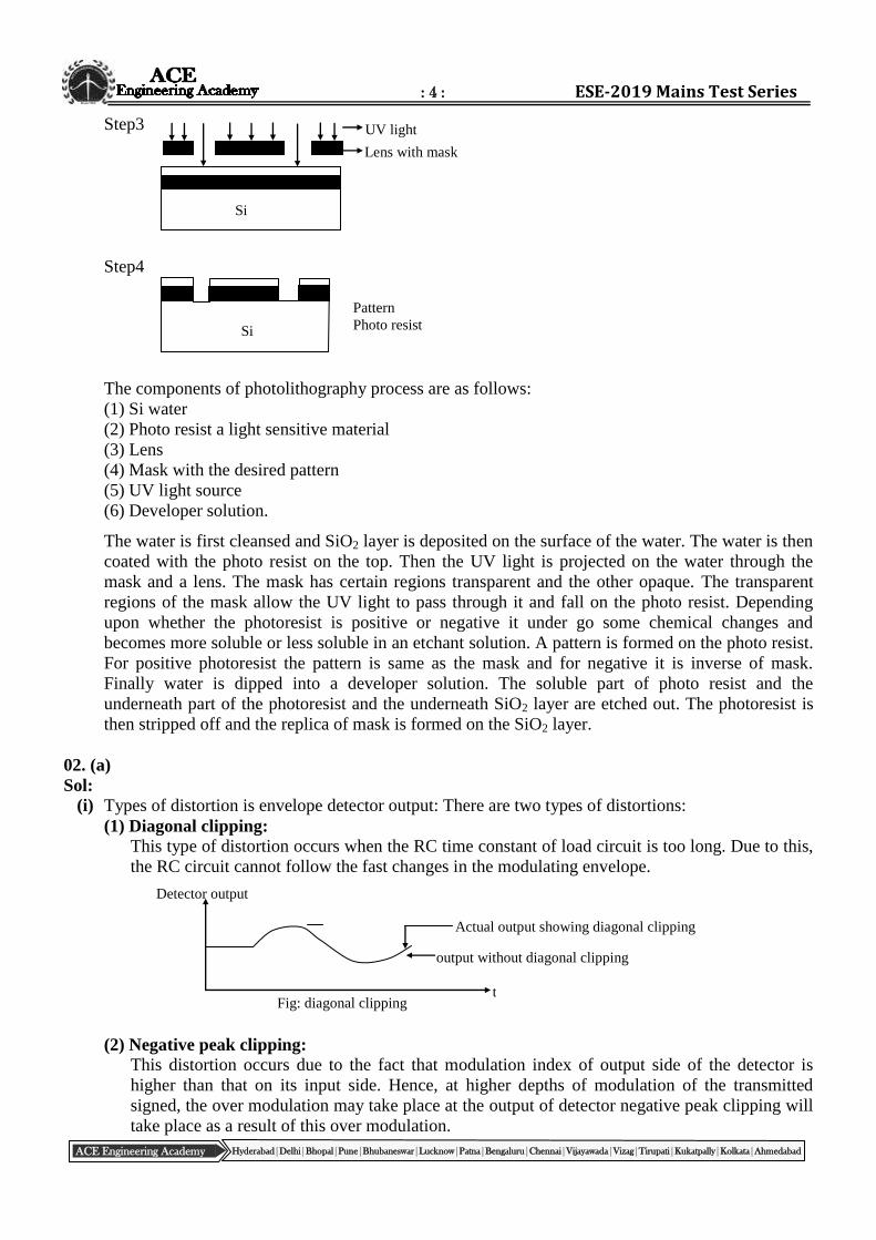
01. (f) Sol: Photo lithography is the technology to create a pattern on the silicon water using an ultraviolet (UV)
ray of light the steps involved in it are shown in below.
Step1
Step2
SiO2 layer Si water
Photo resist
Si
L
0
iLi 1
Z
V1V
: 4 : ESE-2019 Mains Test Series
ACE Engineering Academy Hyderabad|Delhi|Bhopal|Pune|Bhubaneswar|Lucknow|Patna|Bengaluru|Chennai|Vijayawada|Vizag|Tirupati|Kukatpally|Kolkata|Ahmedabad
Step3
Step4
The components of photolithography process are as follows:
(1) Si water
(2) Photo resist a light sensitive material
(3) Lens
(4) Mask with the desired pattern
(5) UV light source
(6) Developer solution.
The water is first cleansed and SiO2 layer is deposited on the surface of the water. The water is then
coated with the photo resist on the top. Then the UV light is projected on the water through the
mask and a lens. The mask has certain regions transparent and the other opaque. The transparent
regions of the mask allow the UV light to pass through it and fall on the photo resist. Depending
upon whether the photoresist is positive or negative it under go some chemical changes and
becomes more soluble or less soluble in an etchant solution. A pattern is formed on the photo resist.
For positive photoresist the pattern is same as the mask and for negative it is inverse of mask.
Finally water is dipped into a developer solution. The soluble part of photo resist and the
underneath part of the photoresist and the underneath SiO2 layer are etched out. The photoresist is
then stripped off and the replica of mask is formed on the SiO2 layer.
02. (a)
Sol:
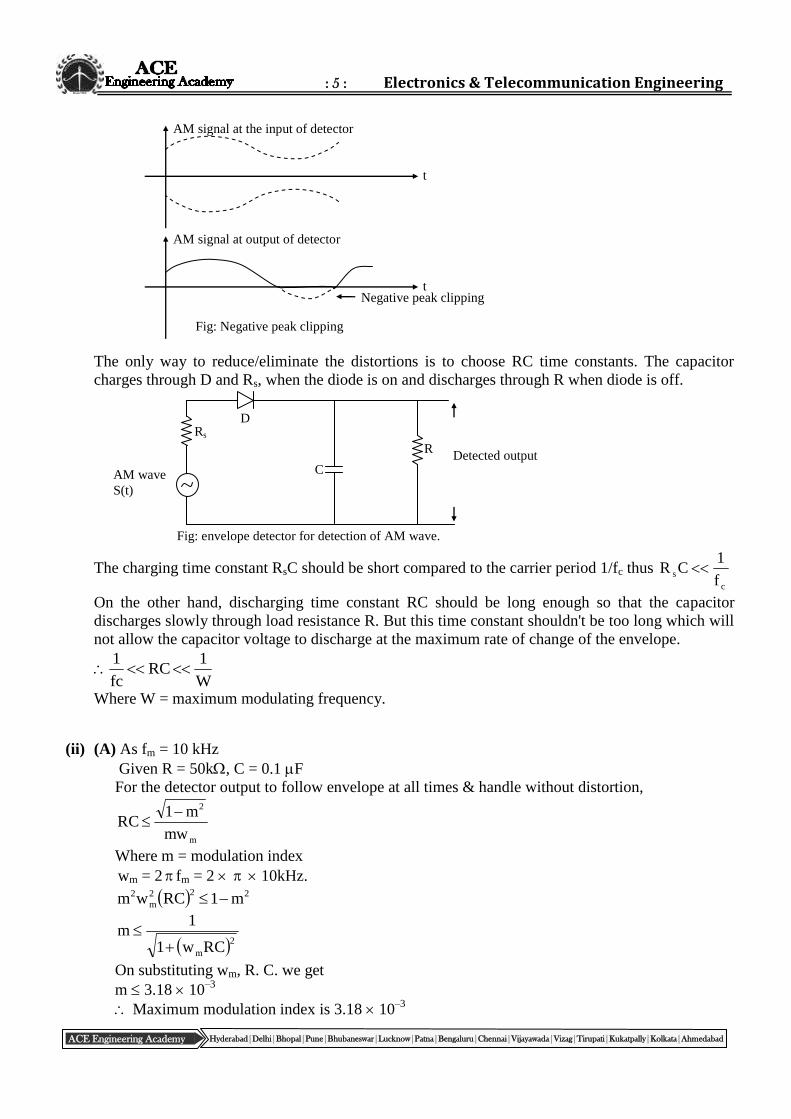
(i) Types of distortion is envelope detector output: There are two types of distortions:
(1) Diagonal clipping:
This type of distortion occurs when the RC time constant of load circuit is too long. Due to this,
the RC circuit cannot follow the fast changes in the modulating envelope.
(2) Negative peak clipping:
This distortion occurs due to the fact that modulation index of output side of the detector is
higher than that on its input side. Hence, at higher depths of modulation of the transmitted
signed, the over modulation may take place at the output of detector negative peak clipping will
take place as a result of this over modulation.
Lens with mask
Si
UV light
Si Si
Pattern
Photo resist
Actual output showing diagonal clipping
output without diagonal clipping
t Fig: diagonal clipping
Detector output
: 5 : Electronics & Telecommunication Engineering
ACE Engineering Academy Hyderabad|Delhi|Bhopal|Pune|Bhubaneswar|Lucknow|Patna|Bengaluru|Chennai|Vijayawada|Vizag|Tirupati|Kukatpally|Kolkata|Ahmedabad
The only way to reduce/eliminate the distortions is to choose RC time constants. The capacitor
charges through D and Rs, when the diode is on and discharges through R when diode is off.
The charging time constant RsC should be short compared to the carrier period 1/fc thus c
sf
1CR
On the other hand, discharging time constant RC should be long enough so that the capacitor
discharges slowly through load resistance R. But this time constant shouldn't be too long which will
not allow the capacitor voltage to discharge at the maximum rate of change of the envelope.
W
1RC
fc
1
Where W = maximum modulating frequency.
(ii) (A) As fm = 10 kHz
Given R = 50k, C = 0.1 F
For the detector output to follow envelope at all times & handle without distortion,
m
2
mw
m1RC
Where m = modulation index
wm = 2 fm = 2 10kHz.
222
m
2 m1RCwm
2mRCw1
1m
On substituting wm, R. C. we get
m 3.18 10–3
Maximum modulation index is 3.18 10–3
AM signal at the input of detector
t
AM signal at output of detector
t Negative peak clipping
Fig: Negative peak clipping
Rs D
AM wave
S(t)
C
R Detected output
Fig: envelope detector for detection of AM wave.

: 6 : ESE-2019 Mains Test Series
ACE Engineering Academy Hyderabad|Delhi|Bhopal|Pune|Bhubaneswar|Lucknow|Patna|Bengaluru|Chennai|Vijayawada|Vizag|Tirupati|Kukatpally|Kolkata|Ahmedabad
(B) When fm = 5 kHz
Similarly m 6.366 10–3
max modulation index = 6.366 10–3
02. (b)
Sol: Put s = j
G (j) =
21
3
jj
jK
G (j) =
32 2
3
j
jK
G (j) =
222
33
)3(2
32
jjK
2
22
23
222
4
32
2
32
3)(
jKKjG
The intersection of G (j) plot with – ive real axis is obtained by equating imaginary part of G
(j) to zero and solving for . Therefore,
0
32
2222
23
K
(2 – 2) = 0
The intersection with –ve real axis occurs at
= 2 rad/sec
The intersection is obtained by substituting = 2 in real part of G (j), i.e.
222
4
2322
2K32j(G
=
23322
2232
K
G 2j = –3
2K
222
3
21
KjG
G (j) = 270 – tan–1 – tan
–1
2
As 0 0jG
G (j) 270
As ∞ |G (j)| ∞
G (j) 90
+ j∞
j0 +
–
–
j0
j∞
s – plane
imj
Re = -0 –1+j0
K3
2
= + 0
= –∞
=+ ∞
Imj
Re
2

: 7 : Electronics & Telecommunication Engineering
ACE Engineering Academy Hyderabad|Delhi|Bhopal|Pune|Bhubaneswar|Lucknow|Patna|Bengaluru|Chennai|Vijayawada|Vizag|Tirupati|Kukatpally|Kolkata|Ahmedabad
The completed Nyquist plot is shown in Figure
It is given that, the number of poles of G(s) having positive real part is nil i.e. P+ = 0.
The encirclements of critical point (–1 + j0) are determined below.
(1) If K< 2
3
The critical point (–1 + j0) lies outside the Nyquist plot, hence N =0
N = P+ – Z +
0 = 0 – Z+
Z+ = Nil
The system is stable
(2) If K > 2
3
The critical point (–1 + j0) will be encircled twice in the clockwise direction by the Nyquist plot,
hence
N = –2
N = P+ – Z +
–2 = 0 Z+
Z+ = 2
The system is unstable.
For stability K 2
3
02. (c)
Sol:
(i) Start
read a, b, c
if a = 0 and b = 0 then
write “illegal equation, cannot solve”
else
if a = 0 then
Set root to −c/b
Write “linear equation, the one root is”, root
else
set discriminant to b2
− 4ac
if discriminant < 0 then
Write “roots are complex, cannot solve”
else
set root -1 to a2
antmindiscrib
set root -2 to a
antdiscrib
2
min
write “answers are “, root-1, root-2
stop
END OF THE ALGORITHM

: 8 : ESE-2019 Mains Test Series
ACE Engineering Academy Hyderabad|Delhi|Bhopal|Pune|Bhubaneswar|Lucknow|Patna|Bengaluru|Chennai|Vijayawada|Vizag|Tirupati|Kukatpally|Kolkata|Ahmedabad
(ii) function power (x:real; n:integer):real;
{compute x raised to the power n recursively the function always returns 0 for x = 0}
begin
if x = 0.0 then
power: = 0.0
else
if n = 0 then
power : = 1.0
else
if n < 0 then
power : = power(x,n+1)/ x
else
power : = power(x,n–1)* x
end; { of power}
03. (a)
Sol:
(i)
0n
nn
n
n
zsin
1nsinr
znxZX
n
0n
1nj1njn
zeesinj2
r
0n
jnj1
0n
jnj1
sinj2
eerz
sinj2
eerz
rzerz1
e
erz1
e
sinj2
1ZX
j1
j
j1
j
j1j1 erz1erz1
1
221 zrcosrz21
1
22
2
rzcosr2z
zZX
(ii) x(2n) = f(n) + g(n)
x(2n+1) = f(n) – g(n)
1N
0n
nkN
2j
e)n(x)k(X
12
N
0n
k)1n2(
N
12
N
0n
Nk2
N W1n2xWn2x
12
N
0n
k1n2
N
12
N
0n
nk2
N WngnfWngnf
: 9 : Electronics & Telecommunication Engineering
ACE Engineering Academy Hyderabad|Delhi|Bhopal|Pune|Bhubaneswar|Lucknow|Patna|Bengaluru|Chennai|Vijayawada|Vizag|Tirupati|Kukatpally|Kolkata|Ahmedabad
12
N
0n
k1n2
N
nk2
N
12
N
0n
k1n2
N
nk2
N WWngWW)n(f
12
N
0n
nk2
N
k
N
12
N
0n
nk2
N
k
N WngW1WnfW1
12
N
0n
nk
2
N
k
N
12
N
0n
nk
2
N
k
N WngW1WnfW1
kGW1kFW1kX k
N
k
N
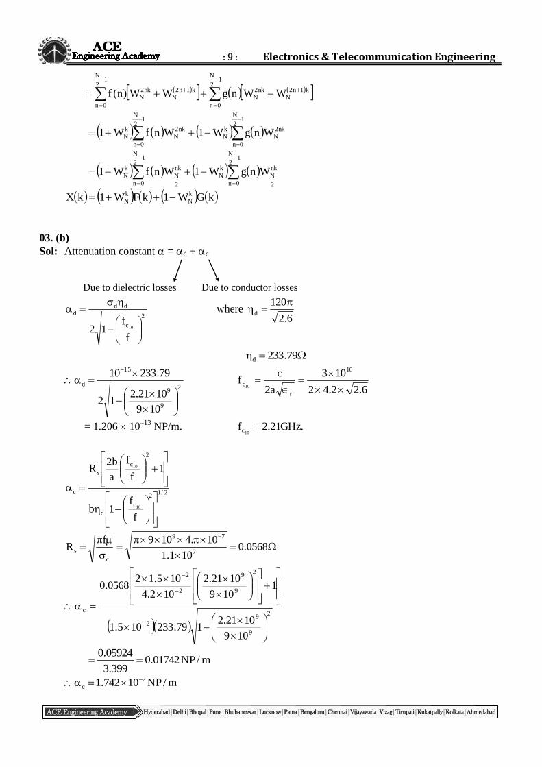
03. (b)
Sol: Attenuation constant = d + c
2
c
ddd
f
f12 10
where
6.2
120d
79.233d
2
9
9
15
d
109
1021.212
79.23310
6.22.42
103
a2
cf
10
r
c10
= 1.206 10–13
NP/m. .GHz21.2f10c
2/1
2
c
d
2
c
s
c
f
f1b
1f
f
a
b2R
10
10
0568.0101.1
10.4109fR
7
79
c
s
2
9
92
2
9
9
2
2
c
109
1021.2179.233105.1
1109
1021.2
102.4
105.120568.0
m/NP01742.0399.3
05924.0
m/NP10742.1 2
c
Due to dielectric losses Due to conductor losses

: 10 : ESE-2019 Mains Test Series
ACE Engineering Academy Hyderabad|Delhi|Bhopal|Pune|Bhubaneswar|Lucknow|Patna|Bengaluru|Chennai|Vijayawada|Vizag|Tirupati|Kukatpally|Kolkata|Ahmedabad
132
dc 10206.110742.1
= 1.74210–2
NP/m
Over 40cm, the attenuation (or) loss will be
40cm = 1.742 10–2
40 10–2
.NP1068.69 4
Attenuation (or) loss in decibels = 69.68 10–4
8.68
= 604.8 10–4
= 60.48 10–3
dB
03. (c)
Sol:
(i) Given n1 = 1.5
= 3 % = 0.03
= 0.82 m
We know that
2
1
2
2
2
1
n2
nn
2
1
2
2
2
1 n.2nn
= 2(1.5)20.03
135.0nn 2
2
2
1
The critical Radius of curvature for the multimode fiber
2/12
2
2
1
2
1c
nn4
n3R
2/1
62
135.04
1082.05.13
Rc = 9 m
(ii) Given that single mode fiber
= 1.55 m
n1 = 1.5
= 0.3 % = 0.03
2
1
2
2
2
1 n2nn
= 20.0032.25
= 0.043
Cut off wavelength for a single - mode fiber is
405.2
2an2 1c
405.2
06.05.1402 6
c
c = 1.214m
Neglect this term

: 11 : Electronics & Telecommunication Engineering
ACE Engineering Academy Hyderabad|Delhi|Bhopal|Pune|Bhubaneswar|Lucknow|Patna|Bengaluru|Chennai|Vijayawada|Vizag|Tirupati|Kukatpally|Kolkata|Ahmedabad
Critical radius of curvature for a single - mode fiber
3
2/12
2
2
1
996.0748.20
cnnRcs
3
6
6
2/1
6
10214.1
1055.1996.0748.2
043.0
1055.120
Rcs = 34mm
04. (a)
Sol:
(i) (A) The delay difference
c
LnT 1
s
8
3
10998.2
01.05.1106
Ts = 300ns
(B) The RMS pulse broadening due to inter model dispersion may be obtained by
C32
Ln1s
8
3
10998.2
01.05.1106
32
1
s = 86.7ns
(C) Maximum bit rate
T2
1BT
sT2
1
910600
1
BT = 1.7Mbps
(or)
9
s
T107.86
2.02.0B
BT = 2.3Mbps
(D) The most accurate estimate of the maximum bit rate is
BT L = 2.3M6km
= 13.8MHz - km
(ii) For down link
Rlog10Mlog10N
E
N
C
o
b
o
Where M = margin
R = bit rate
10log10M = 85 – 10 – 10log(107)

: 12 : ESE-2019 Mains Test Series
ACE Engineering Academy Hyderabad|Delhi|Bhopal|Pune|Bhubaneswar|Lucknow|Patna|Bengaluru|Chennai|Vijayawada|Vizag|Tirupati|Kukatpally|Kolkata|Ahmedabad
10log10M = 5 dB
We also know that
klog10MPT
GEIRP
N
CL
r
dBo
PL = 92.4 + 20log10(12.5) + 20log10(40,000)
PL = –206 dB
10log10(k) = 10log(1.3810–23
)
= –228.6 dB
56.2282065785T
G
dB
r
dB4.10T
G
dB
r
Gr = 10.4 + 10log10(310) (∵ T = 310k)
Gr = 3396.25
For dish antenna
2
2 DG
2
2 D55.025.3396
(∵
125
3 )
25D
125
325d
5
3
D = 0.6m
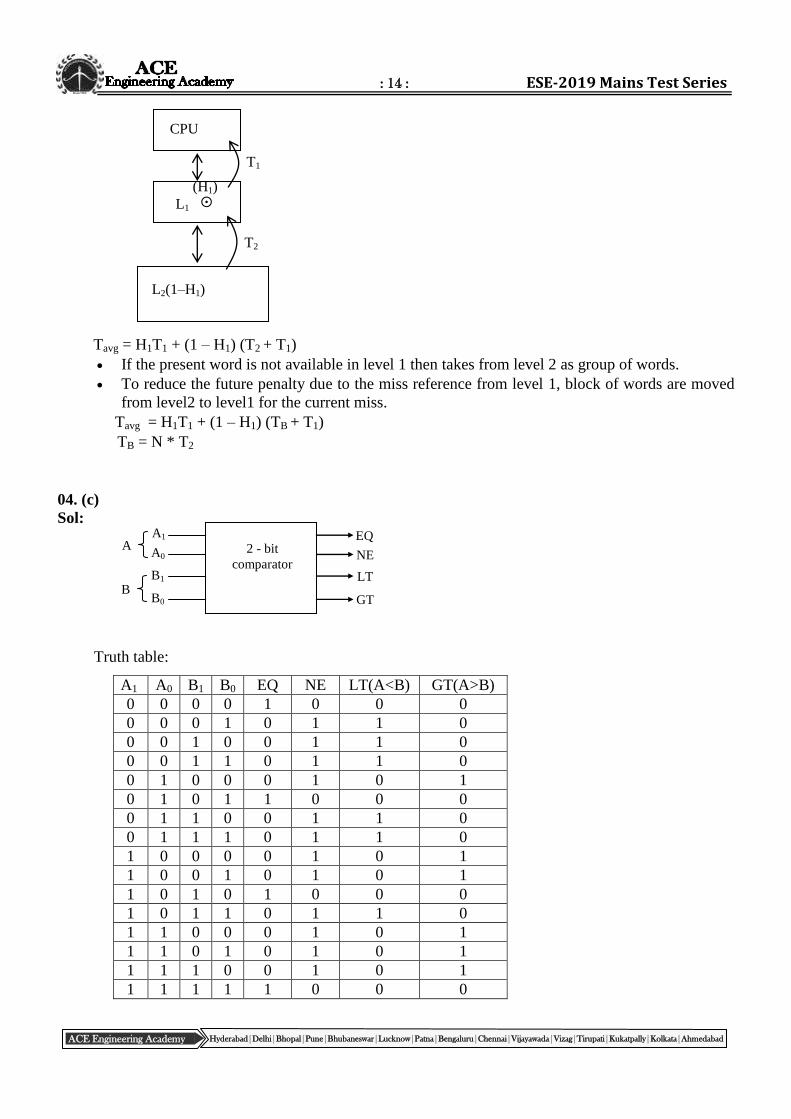
04. (b)
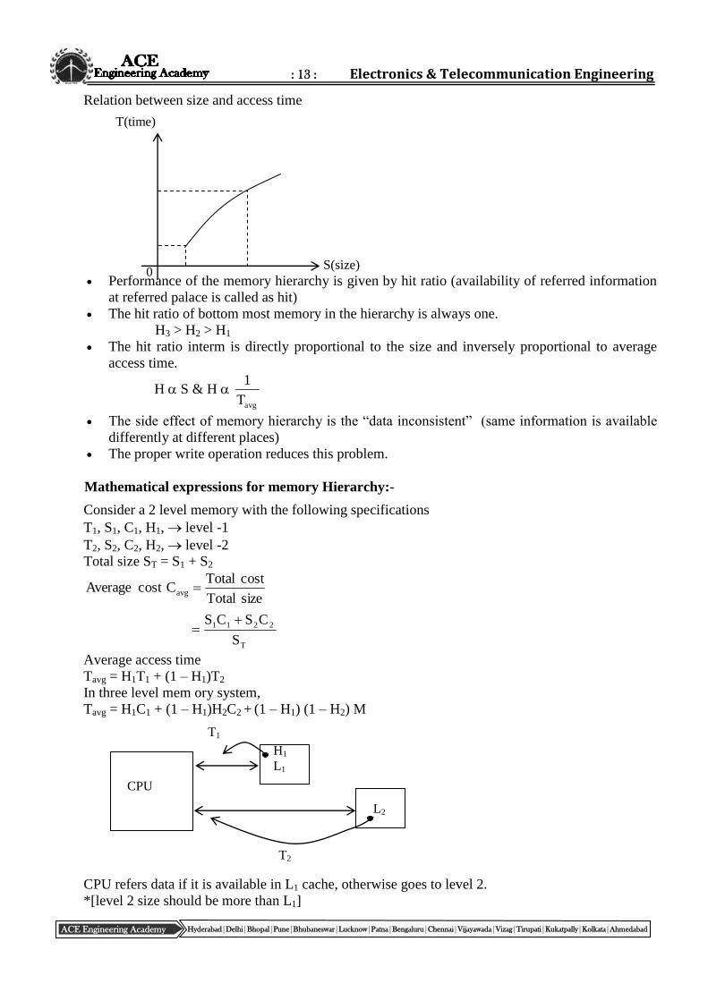
Sol: Objective: To reduce average access time by reducing the overall system cost
The structure of memory hierarchy has different memories of different capacities are organized
such that ith
level memory is placed above (i+1)th
level memory.
Ti < Ti+1 (access time)
Si < Si+1 (size)
Ci > Ci+1 (cost per bit)
fi > fi+1 (frequency of accessing)
Ii Ii + 1 (information)
T , S, C, f
Cache
memory
H1
Main memory H2
Disk memory H3 H = 1
DMA
2
1
0
: 13 : Electronics & Telecommunication Engineering
ACE Engineering Academy Hyderabad|Delhi|Bhopal|Pune|Bhubaneswar|Lucknow|Patna|Bengaluru|Chennai|Vijayawada|Vizag|Tirupati|Kukatpally|Kolkata|Ahmedabad
Relation between size and access time
Performance of the memory hierarchy is given by hit ratio (availability of referred information
at referred palace is called as hit)
The hit ratio of bottom most memory in the hierarchy is always one.
H3 > H2 > H1
The hit ratio interm is directly proportional to the size and inversely proportional to average
access time.
H S & H avgT
1
The side effect of memory hierarchy is the “data inconsistent” (same information is available
differently at different places)
The proper write operation reduces this problem.
Mathematical expressions for memory Hierarchy:-
Consider a 2 level memory with the following specifications
T1, S1, C1, H1, level -1
T2, S2, C2, H2, level -2
Total size ST = S1 + S2
sizeTotal
costTotalCcostAverage avg
T
2211
S
CSCS
Average access time
Tavg = H1T1 + (1 – H1)T2
In three level mem ory system, Tavg = H1C1 + (1 – H1)H2C2 + (1 – H1) (1 – H2) M
CPU refers data if it is available in L1 cache, otherwise goes to level 2.
*[level 2 size should be more than L1]
T(time)
0 S(size)
CPU
H1
L1
T1
L2
T2
: 14 : ESE-2019 Mains Test Series
ACE Engineering Academy Hyderabad|Delhi|Bhopal|Pune|Bhubaneswar|Lucknow|Patna|Bengaluru|Chennai|Vijayawada|Vizag|Tirupati|Kukatpally|Kolkata|Ahmedabad
Tavg = H1T1 + (1 – H1) (T2 + T1)
If the present word is not available in level 1 then takes from level 2 as group of words.
To reduce the future penalty due to the miss reference from level 1, block of words are moved
from level2 to level1 for the current miss.
Tavg = H1T1 + (1 – H1) (TB + T1)
TB = N * T2
04. (c)
Sol:
Truth table:
A1 A0 B1 B0 EQ NE LT(A<B) GT(A>B)
0 0 0 0 1 0 0 0
0 0 0 1 0 1 1 0
0 0 1 0 0 1 1 0
0 0 1 1 0 1 1 0
0 1 0 0 0 1 0 1
0 1 0 1 1 0 0 0
0 1 1 0 0 1 1 0
0 1 1 1 0 1 1 0
1 0 0 0 0 1 0 1
1 0 0 1 0 1 0 1
1 0 1 0 1 0 0 0
1 0 1 1 0 1 1 0
1 1 0 0 0 1 0 1
1 1 0 1 0 1 0 1
1 1 1 0 0 1 0 1
1 1 1 1 1 0 0 0
A1
A0
B0
B1
A
B
2 - bit
comparator
EQ
NE
LT
GT
CPU
T1
T2
L1
L2(1–H1)
(H1)

: 15 : Electronics & Telecommunication Engineering
ACE Engineering Academy Hyderabad|Delhi|Bhopal|Pune|Bhubaneswar|Lucknow|Patna|Bengaluru|Chennai|Vijayawada|Vizag|Tirupati|Kukatpally|Kolkata|Ahmedabad
K - map for EQ: K - map for NE:
01010101 BBAABBAAEQ 11110000 BABABABANE
01010101 BBAABBAA
K - map for GT: K - map for LT
00101011 BAABBABAGT 01000111 BBABAABALT
Common SOPs are ,BA,BA 1111
Logic diagram using PLA:
In PLA both AND and OR gates are programmable
A1A0
B1B0 00
00
01
01
11
11 10
10
1
1
1
1
A1A0
B1B0 00
00
01
01
11
11 10
10
1 1 1
1 1
1
1 1 1
1
1
1
A1A0
B1B0 00
00
01
01
11
11 10
10
1
1 1
1
1
1
A1A0 B1B0
00
00
01
01
11
11 10
10
1
1 1
1
1
1
A1 A0 B1 B0
EQ NE GT LT

: 16 : ESE-2019 Mains Test Series
ACE Engineering Academy Hyderabad|Delhi|Bhopal|Pune|Bhubaneswar|Lucknow|Patna|Bengaluru|Chennai|Vijayawada|Vizag|Tirupati|Kukatpally|Kolkata|Ahmedabad
05. (a)
Sol:
(i) Path loss exponent r = 6
First, let cluster size N = 7
Co-channel reuse ratio 583.4N3R
Dq
rq6
1
I
C
6583.46
1
35.1544I
C
35.1544log10I
C
dB
dB6dB88.31I
C
dB
Since this is greater than minimum required ,I
C N = 7 can be used.
(ii) Path loss exponent r = 2
Let N = 7
rq6
1
I
C
2583.46
1
= 3.5
dB6dB44.5I
C
dB
Which is less than minimum required ,I
C hence we need to use larger N.
Next possible value of N = 12 for i = j = 2
6123N3q
rq6
1
I
C
26
6
1
6I
C
dB6dB78.7I
C
dB
Since this is greater than minimum required ,I
C N = 12 can be used.

: 17 : Electronics & Telecommunication Engineering
ACE Engineering Academy Hyderabad|Delhi|Bhopal|Pune|Bhubaneswar|Lucknow|Patna|Bengaluru|Chennai|Vijayawada|Vizag|Tirupati|Kukatpally|Kolkata|Ahmedabad
05. (b)
Sol:
From the diagram the third charge ‘q’ is placed at a distance of ‘x’ from charge +3Q
For the system to be in equilibrium, q must be negative
F12 = F23 = F13
)1____(d4
Q3
x4
Qq3
xd4
Qq2
o
2
2
o
2
o
That is, 3(d–x)2 = x
2
3d2 – 6dx + 3x
2 = x
2
2x2 – 6dx + 3d
2 = 0
4
12dd6x
When d = 2, x = 4.73m or 1.268m
As x<d, x = 1.268m is considered.
Substitute x = 1.268 in equation (1)
2
o
2
2
o d4
Q3
x4
Qq3
Q = –Q(x2/d
2)
q = – 0.4Q
Location of third charge is 1.268m from +3Q towards +Q and the value of charge is – 0.4Q.
05. (c)
Sol: (i) An address on a paging system is a logical page number and an offset. The physical page is found
by searching a table based on the logical page number to produce a physical page number. Because
the operating system controls the contents of this table, it can limit a process to accessing only those
physical pages allocated to the process. There is no way for a process to refer to a page it does not
own because the page will not be in the page table. To allow such access, an operating system
simply needs to allow entries for non-process memory to be added to the process’s page table. This
is useful when two or more processes need to exchange data—they just read and write to the same
physical addresses (which may be at varying logical addresses). This makes for very efficient inter
process communication.
(ii) As such, C programming does not provide direct support for error handling but being a system
programming language, it provides you access at lower level in the form of return values. Most of
the C or even Unix function calls return –1 or NULL in case of any error and set an error code errno.
It is set as a global variable and indicates an error occurred during any function call. You can find
various error codes defined in <error.h> header file.
(2m)
+Q +3Q
d
q x

: 18 : ESE-2019 Mains Test Series
ACE Engineering Academy Hyderabad|Delhi|Bhopal|Pune|Bhubaneswar|Lucknow|Patna|Bengaluru|Chennai|Vijayawada|Vizag|Tirupati|Kukatpally|Kolkata|Ahmedabad
So a C programmer can check the returned values and can take appropriate action depending on the
return value. It is a good practice, to set errno to 0 at the time of initializing a program. A value of 0
indicates that there is no error in the program.
The C programming language provides perror() and strerror() functions which can be used to display
the text message associated with errno.
The perror() function displays the string you pass to it, followed by a colon, a space, and then the
textual representation of the current errno value.
The strerror() function, which returns a pointer to the textual representation of the current errno
value.
05. (d)
Sol: %Mp = 21
e ×100
26 =21
e ×100
21 ζ
ζπ
e
= 26
100
21
= 1.34
1 – 2 =
2
34.1
1– 2 = 5.49
2
2 =
49.51
1
= 39.049.6
1
Resonant frequency:
r = n 221
8 = n 221 = n
239.021
= n 699.0
n =
699.0
8 = 9.6 rad/sec
The overall transfer function is
1.
1STs
K1
1STs
K
sHsG1
sG
sR
sC)s(M
=
T
Ks
T
1s
T/K
KsTs
K
22
The characteristic equation is
s2
+ 0T
Ks
T
1
: 19 : Electronics & Telecommunication Engineering
ACE Engineering Academy Hyderabad|Delhi|Bhopal|Pune|Bhubaneswar|Lucknow|Patna|Bengaluru|Chennai|Vijayawada|Vizag|Tirupati|Kukatpally|Kolkata|Ahmedabad
On comparing above equation with s2
+ 2 ns + 02 n (characteristic equation of a second order
system)
2 n = T
1
T = 13.06.939.02
1
2
1
n
and T
Kn 2
K = T2
n = (9.6)2 (0.13) = 11.9
Resonant peak :
Mr = 212
1
= 239.0139.02
1
= 1.39
Gain crossover frequency:
1 = n 22/14 214
= 8.69 22/14 39.02139.04
= 8.69 74.0 = 7.47 rad/sec
Phase margin = tan –1
22/14 214
2
�
= tan –1
22/14 39.02139.04
39.02
= tan
–1 ( 1.054 )
= 46.5
05. (e) Sol: The bit duration is
s4.0Hz105.2
1T
6b
The signal energy per bit is
b
2
Cb TA2
1E
= 1366 102104.0102
1 joules
(i) Coherent Binary FSK
The average probability of error is
0be N2/Eerfc2
1P

: 20 : ESE-2019 Mains Test Series
ACE Engineering Academy Hyderabad|Delhi|Bhopal|Pune|Bhubaneswar|Lucknow|Patna|Bengaluru|Chennai|Vijayawada|Vizag|Tirupati|Kukatpally|Kolkata|Ahmedabad
= 2013 104/102erfc2
1
= 6105erfc2
1
Using the approximation
`u
uexpuerfc
2
We obtain the result
6
6
e
105
105exp
2
1P
(ii) MSK
0be N/EfcerP
= erfc 61010
6
6
1010
)1010exp(
(iii) Non-coherent Binary FSK
0
be
N2
Eexp
2
1P
= )105exp(2
1 6
06. (a)
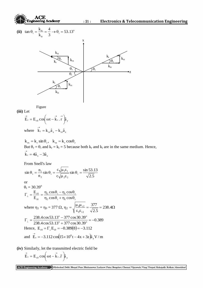
Sol:
(i) From the incident
E field, it is evident that the propagation vector is
c
5ka3a4k 00izxi
Hence,
= 5c = 15 108 rad/s
A unit vector normal to the interface (z = 0) is za . The plane containing
k and za is y = constant
which is xz-plane, the plane of incidence, since iE
is normal to this plane, so perpendicular
polarization .
: 21 : Electronics & Telecommunication Engineering
ACE Engineering Academy Hyderabad|Delhi|Bhopal|Pune|Bhubaneswar|Lucknow|Patna|Bengaluru|Chennai|Vijayawada|Vizag|Tirupati|Kukatpally|Kolkata|Ahmedabad
(ii) o
i
iz
ixi 13.53
3
4
k
ktan
(iii) Let
yr0rr ar.ktcosEE
where zrzxrxr akakk
rrrzrrrx coskk,sinkk
But r = i and kr = ki = 5 because both kr and ki are in the same medium. Hence,
zxr a3a4k
From Snell's law
i
22
11
i
2
1t sin
c
csin
n
nsin
5.2
13.53sin
or
t = 30.39o
0i
0r
E
E
t1i2
t1i2
coscos
coscos
where 1 = 0 = 377 , 2
4.238
5.2
377
2r0
2r0
389.039.30cos37713.53cos4.238
39.30cos37713.53cos4.238oo
oo
Hence, 112.38389.0EE 0i0r
and m/Vaz3x4t1015cos112.3E y
8r
(iv) Similarly, let the transmitted electric field be
yt0tt ar.ktcosEE
i kix
kiz
ki
i
r t
t
kt
ktz
ktx
krz
kr krx
r
z
Figure
x

: 22 : ESE-2019 Mains Test Series
ACE Engineering Academy Hyderabad|Delhi|Bhopal|Pune|Bhubaneswar|Lucknow|Patna|Bengaluru|Chennai|Vijayawada|Vizag|Tirupati|Kukatpally|Kolkata|Ahmedabad
where
22 rr222t
ck
906.75.21103
10158
8
From Figure
4sinkk tttx
819.6coskk tttz
or
zxt a819.6a4k
t1i2
i2
0i
0t
coscos
cos2
E
E
611.039.30cos37713.53cos4.238
13.53cos4.2382oo
o
Hence
Et0 = Ei0 = 0.611 8 = 4.888
tE
= 4.888 cos(15 108t – 4x – 6.819z) m/Va y
2
tktt
2
i
EaEk
1H t
r.ktcosa888.44.238906.7
a819.6a4y
zx
m/mAz819.6x4t1015cosa37.10a69.17H 8
zxt
06. (b)
Sol:
(i) For T = 0 and K =1 determine the gain cross over frequency 1
G(j) = 7j1jj
10
At the phase crossover frequency
= 1; |G (j1) | = 1.
17j1jj
10
111
171
10
22
1
22
11
1491
10
2
1
2
11
By inspection 1 = 1 rad/sec
G(j) = – 90 – tan–1
1tan
–1
7
: 23 : Electronics & Telecommunication Engineering
ACE Engineering Academy Hyderabad|Delhi|Bhopal|Pune|Bhubaneswar|Lucknow|Patna|Bengaluru|Chennai|Vijayawada|Vizag|Tirupati|Kukatpally|Kolkata|Ahmedabad
G (j1) = – 90 – tan
–11 – tan
–1 7
1
1 = 1 rad/ sec
G (j1) = – 90 – tan–1
1 – tan–1
7
1
= – 90 – 45 – 8.13 = – 141.13
Incorporating time delay element e–jT,
the condition for marginal stability is given below:
G (j1) + e–jT
= – 180
–141.13 –
180T1 = –180
∵ 1 = 1 rad/sec
–141.13 – 180180T1
678.01801
13.141180
T sec
(ii) T = 1 sec
G(s) = 71
10 1.
sss
Ke s
Put s = j
G(j) = 7)1(
10
jjj
Ke j
G(j) = –
180 – 90 – tan
–1
7tan
1
1
= –
180–90 – tan
–1
7.1
7
= –
180–90 – tan
–1
27
8
; < 7
At the phase cross over frequency 2, G(j2) = – 180
1807
8tan90
1802
2
212
ω
= – 57.32 – tan–1
2
2
2
7
8
= – 90
Solving by trial –error method: 2 = 0.79 rad/sec
71
10
222
2
jjj
KjG
= 22
2
22
22 71
K10
2 = 0.79 rad/sec

: 24 : ESE-2019 Mains Test Series
ACE Engineering Academy Hyderabad|Delhi|Bhopal|Pune|Bhubaneswar|Lucknow|Patna|Bengaluru|Chennai|Vijayawada|Vizag|Tirupati|Kukatpally|Kolkata|Ahmedabad
708.0
K
779.0179.079.0
K10079.0jG
22222
For stability 708.0
K<1; K < 0.708
For marginally stability: K = 0.708
06. (c)
Sol:
(i) We have
deX2
1tx tj
tx2deX tj
Substituting t = 0 in the above equation, we get
0x2dX = 2 (1) = 2
(ii) From Parsavel's theorem, we have
dX2
1dttx
22
3
831122
3
2
22
0
20
1
222
dttdttdttdttxdX
(iii) We have tx2deX tj
Substituting t = 2, we get
2x2deX 2j
= 2 (–1) = –2
(iv) We have
dtetxX tj
Substituting = 0, we get
dttx0X
= 0 [ x(t) is a shifted odd signal]
07. (a)
Sol:
(i) If the transfer function has symmetric pole and zero about the imaginary axis in s - plane then the
transfer function is called all pass transfer function and given by
G(s) = sT
sT
1
1

: 25 : Electronics & Telecommunication Engineering
ACE Engineering Academy Hyderabad|Delhi|Bhopal|Pune|Bhubaneswar|Lucknow|Patna|Bengaluru|Chennai|Vijayawada|Vizag|Tirupati|Kukatpally|Kolkata|Ahmedabad
In sinusoidal form above transfer function is written as
G(j) =Tj
Tj
1
1
The pole - zero configuration and Bode plot for all pass transfer function is shown in Figure
The magnitude plot lies on 0 db axis indicating that the actual gain for the frequencies is 1, thus
the transfer function passes all frequencies.
The phase angle for all pass transfer function is given by
Tj1
Tj1
= tan
–1 (–T) – tan
–1 (T) = –2 tan
–1 (T)
The phase angle for all pass transfer functions given by –2 tan–1
(T) and
varies from 0 to –180 as the frequency is varied from = 0 to = ∞
(ii) s5
+ s4
+ 2 s3 + 2s
2 +11s +10 = 0
s5 1 2 11
s4 1 2 10
s3 0 1 0
s2 0.227 10 0
While forming the Routh array as above the third element in the first column is zero and thus the
Routh criterion fails at this stage. The difficulty is solved if zero in the third row of the first
column is replaced by a symbol and Routh array is formed as follows
+ s5 1 2 11
+ s4 1 2 10
+ S3 1 0
s2
112lim
0
10 0
+ s1
112
101lim
2
0
0 0
+ s0 10
The limits of fourth and fifth element in the first column a 0 from positive side are – ∞ and
+1 respectively, indicating two sign changes, therefore, the system is unstable and the number of
roots with positive real part of the characteristic equation is 2.
Re
Img
T
1 T
1
Pole –zero configuration
G(j)
0 dB
0
– 90G(j)
– 180
Bode plot for all pass transfer function
jG
|G(j
)|d
B

: 26 : ESE-2019 Mains Test Series
ACE Engineering Academy Hyderabad|Delhi|Bhopal|Pune|Bhubaneswar|Lucknow|Patna|Bengaluru|Chennai|Vijayawada|Vizag|Tirupati|Kukatpally|Kolkata|Ahmedabad
07. (b)
Sol:
(i) If the received signal is Km(t)cosct, the demodulator input is [Km(t) + nc(t)]cosct + ns(t)sinct.
When this is multiplied by 2 cosct and low-pass filtered the output is
So(t) + no(t) = km(t) + nc(t)
Signal power 22
o mKS
Noise pwer 2
co nN
But the power of the received signal km(t) cosct is 1W. Hence,
6
22
102
mK
622
o 102mKS
To compute 22
c nn
Where 2n is the power of the incoming bandpass noise of bandwidth 8 kHz centered at 500 kHz.
i.e.,
da
1
2
2n
5040002
4960002
22
2
5040002
4960002
1
atan
a
11
6
1
6
1
6 10
4960002tan
10
5040002tan
10
1
780.0788.014.310
126
= 8.113 10–10
= No
17.246510113.8
102
N
S10
6
o
o
= 33.83 dB
(ii) Generator matrix G = [Ik|P]
Where Ik is kk identity matrix
P is k(n – k) matrix
Parity check matrix H = [PT|In-k]
G is a kn matrix
H is a (n-k) n matrix.
0PPI
PPIGH
m
K
T
07. (c)
Sol: Assume, x(n) = x1(n) Ⓝ x2(n)
Apply DFT on both sides
X(k) = X1(k) X2(k)

: 27 : Electronics & Telecommunication Engineering
ACE Engineering Academy Hyderabad|Delhi|Bhopal|Pune|Bhubaneswar|Lucknow|Patna|Bengaluru|Chennai|Vijayawada|Vizag|Tirupati|Kukatpally|Kolkata|Ahmedabad
1Nto0k,enxkX1N
0n
nkN
2j
11
N = 4
5nx0X3
0n
11
1enx1X3
0n
2
nj
11
1enx2X3
0n
jn
11
1enx3X3
0n
2
n3j
11
X1(k) = {5, –1, 1, –1}
1Nto0k,enxkX1N
0n
nkN
2j
22
N = 4
10nx0X3
0n
22
2j2enx1X3
0n
2
nj
22
2enx2X3
0n
jn
22
2j2enx3X3
0n
2
n3j
22
X2(k) = {10, –2 + j2, –2, –2 – j2}
X3(k) = X1(k) X2(k) = {50, 2 – j2, –2, 2 + j2}
IDFT of X3(k) is 1Nto0k,ekXN
1nx
1N
0k
nkN
2j
33
3
0k
33 13kX4
10x
3
0k
2
kj
33 14ekX4
11x
3
0k
kj
33 11ekX4
12x
3
0k
2
k3j
33 12ekX4
13x
x3(n) = {13, 14, 11, 12,}.

: 28 : ESE-2019 Mains Test Series
ACE Engineering Academy Hyderabad|Delhi|Bhopal|Pune|Bhubaneswar|Lucknow|Patna|Bengaluru|Chennai|Vijayawada|Vizag|Tirupati|Kukatpally|Kolkata|Ahmedabad
08. (a)
Sol:
(i) The waveform shown in Figure is periodic with a period T = 2.
Let, t0 = 0, t0 + T = 2
Then, Fundamental frequency 12
2
T
20
The waveform is described by
2tfor0
t0fort/Atx
T
0
2
0
0 dttx2
1dttx
T
1a
4
A
2
t
2
Adtt
A
2
1
0
2
0
2
T
0
0n dttncostxT
2a
0 0
2dtntcost
Adtntcost
A
2
2
0
22
00
2 n
ntcos
n
00Adt
n
ntsin
n
ntsintA
0cosncosn
A22
nevenfor;0
noddfor;n/A2a
22
n
T
0
0n dttnsintxT
2b
2
0 0
dtntsintA1
dtntsintx2
2
000
22dt
n
ntcos
n
ntcostAdtntsint
A
0
22 n
ntsin
n
ncosA
1n1
n
Ancos
n
A
nevenfor;n/A
noddfor;n/Abn
The trigonometric Fourier is:
tnsinbtncosaatx 0n0
1n
n0

: 29 : Electronics & Telecommunication Engineering
ACE Engineering Academy Hyderabad|Delhi|Bhopal|Pune|Bhubaneswar|Lucknow|Patna|Bengaluru|Chennai|Vijayawada|Vizag|Tirupati|Kukatpally|Kolkata|Ahmedabad
1n
1n
oddn22 n
ntsin)1(
A
n
ntcosA2
4
A
....t5cos
5
1t3cos
3
1tcos
A2
4
A222
....t4sin
4
1t3sin
3
1t2sin
2
1tsin
A
(ii) The signal shown in Figure is expressed as:
whereelse;0
Tt0for;A
0tTfor;A
tx
dtetxX tj
dtAedtAedtAedtAe
T
0
tj
T
0
tj
T
0
tj
0
T
tj
0Tj0Tj
T
0
tjT
0
tj
eeeej
A
j
eA
j
eA
Tcos1j
A2Tcos22
j
Aee2
j
A TjTj
Therefore, the magnitude of X() is:
Tcos1A2
X
|X()| = 0, when 1 – cos T = 0
i.e. T = 2n or T
n2
The magnitude spectrum is as shown in Figure.
08. (b)
Sol:
(i) The noise figure of the lossy cable is 3 dB = 100.3
= 2.
The gain factor, of the cable is 5.02
1
21
3
1
21
GG
1F
G
1FFF
Where F1 = 100.6
= 3.98
T
6
|X()|
0
T
4 T
2
T
2 T
4 T
6

: 30 : ESE-2019 Mains Test Series
ACE Engineering Academy Hyderabad|Delhi|Bhopal|Pune|Bhubaneswar|Lucknow|Patna|Bengaluru|Chennai|Vijayawada|Vizag|Tirupati|Kukatpally|Kolkata|Ahmedabad
C(s) R(s)
– s)K2(s
t
2
nn
2
2
n
+
G1 = 100
F2 = 2, G2 = 0.5
F3 = 101.6
= 39.8,
Substituting F = 3.98 + 5.0100
18.39
100
12
= 3.98 + 0.01 + 0.776
= 4.766 + 10 log104.766 = 6.8 dB
(ii) Upon removal of the pre-amplifier there are 2 blocks only the cable and the front end
Now F1= 2 , F2 = 39.8
1
11
G
1FFF
= dB196.795.0
18.392
This shows the need of placing the pre-amplifier before the begin of the lossy line. The front end
receiver gain has no contribution in reducing the noise figure.
(iii) When the amplifier is placed after the cable, is the first stage
21
2
1
21
GG
1F
G
1FFF
5.0100
18.39
5.0
198.32
= 2 + 5.96 + 0.776
= 8.736
= 9.4 dB
Thus the Noise figure changes by 2.6dB.
08. (c) Sol: (i)
From the block diagram figure the transfer function for a unity feedback second order – control
system using derivate feedback control is determined below:
1.
sK2s1
s)K2(s
sR
sC
t
2
nn
2
2
n
t
2
nn
2
2
n
2
nt
2
nn
2
2
n
s)K2(ssR
sC
The characteristic equation for the overall transfer function is
s2
+ (2 n + 2
n Kt)s + 2
n = 0
The damping ratio for the above characteristic equation is

: 31 : Electronics & Telecommunication Engineering
ACE Engineering Academy Hyderabad|Delhi|Bhopal|Pune|Bhubaneswar|Lucknow|Patna|Bengaluru|Chennai|Vijayawada|Vizag|Tirupati|Kukatpally|Kolkata|Ahmedabad
n
t
2
nn'
2
K2
2
Ktn'
The damping ratio is increased by using derivative feedback control and therefore, the maximum
overshoot is decreased. However, the rise time is increased.
(ii) In the block diagram figure the forward path transfer function is
G(s) = sK2s t
2
nn
2
2
n
and the feedback path transfer function is H (s) = 1
The transfer function relating E(s) and R(s) is given by
)()(1
1
sHsGsR
sE
Substituting
G(s) = sKs tnn
n
22
2
2
and H (s) = 1 in )()(1
1
sHsGsR
sE
the following relation between the error and input signal for
the derivative feedback control action is obtained
1.s)K2(s
1
1
sR
sE
t
2
nn
2
2
n
2
nt
2
nn
2
t
2
nn
2
sK2s
sK2s
sR
sE
For a unit ramp function
R (s) = 1/s2
E(s) =
2
nt
2
nn
2
t
2
nn
2
2 s)K2(s
sK2s.
s
1
The steady state error is determined below:
ess = 0
lims
s E(s)
2
nt
2
nn
2
t
2
nn
2
20s sK2s
sK2s.
s
1.sLim
ess = t
n
K2
I2
2.16 9.7
3.0433.4
3/4