a programmable imager for very high speed cellular signal processing
TRANSCRIPT
Journal of VLSI Signal Processing 23, 305–318 (1999)c© 1999 Kluwer Academic Publishers. Manufactured in The Netherlands.
A Programmable Imager for Very High Speed Cellular Signal Processing
ELISENDA ROCAInstituto de Microelectronica de Sevilla, Centro Nacional de Microelectronica, Avda. Reina Mercedes s/n,
Campus Universidad de Sevilla, E-41012 Sevilla, Spain
SERVANDO ESPEJO, RAFAEL DOMINGUEZ-CASTRO, GUSTAVO LINANAND ANGEL RODRIGUEZ-VAZQUEZ
Instituto de Microelectronica de Sevilla, Centro Nacional de Microelectronica, Avda. Reina Mercedes s/n,Campus Universidad de Sevilla, E-41012 Sevilla, Spain; Area de Electronica, Escuela Superior de Ingenieros,
Universidad de Sevilla, Camino de los Descubrimientos s/n, Isla de la Cartuja, E-41092 Sevilla, Spain
Abstract. In this paper a programmable imager with averaging will be described which is intended for averagingof different groups or sets of pixels formed byn× n kernels,n×m kernels or independent pixels of the array. Thisimager is a 64× 64 array which uses passive pixels that can be randomly accessed. The read-out stage includesa sole charge amplifier with programmable gain, a sample-and-hold structure and an analog buffer. This read-out structure is different from other existing imagers with variable resolution since it uses a sole charge amplifier,whereas the normal structure is an operational amplifier per column plus a global operational amplifier. Thisstructure will be described in detail indicating the advantages and disadvantages with respect to other imagers withaveraging capabilities. This programmable resolution architecture can be more appropriate, and eventually, moreefficient, when implementing very high speed Cellular Neural Network (CNN) processors in a CNN chipset —amixed-signal hardware platform for CNN-based image processing. A significant processing time reduction can beobtained when decreasing the image resolution, and therefore the amount of information to be transferred to theCNN processor. This programmable resolution can also be used for fast image recognition and ulterior windowingat full resolution in a reduced area of the image, permitting a more accurate processing of the region of interest. Inaddition, full resolution images can still be obtained, as in commercial imagers which are usually included in CNNchipsets.
1. Introduction
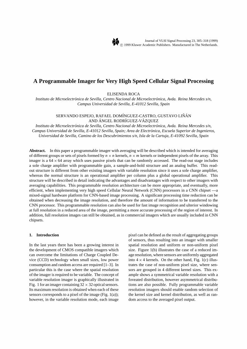
In the last years there has been a growing interest inthe development of CMOS compatible imagers whichcan overcome the limitations of Charge Coupled De-vice (CCD) technology when small sizes, low powerconsumption and random access are required [1–3]. Inparticular this is the case where the spatial resolutionof the imager is required to be variable. The concept ofvariable resolution imager is graphically illustrated inFig. 1 for an imager containing 32× 32 optical sensors.Its maximum resolution is obtained when each of thesesensors corresponds to a pixel of the image (Fig. 1(a));however, in the variable resolution mode, each image
pixel can be defined as the result of aggregating groupsof sensors, thus resulting into an imager with smallerspatial resolution and uniform or non-uniform pixelsize. Figure 1(b) illustrates the case of a reduced im-age resolution, where sensors are uniformly aggregatedinto 4× 4 kernels. On the other hand, Fig. 1(c) illus-trates the case of non-uniform pixel size, where sen-sors are grouped in 4 different kernel sizes. This ex-ample shows a symmetrical variable resolution with afoveated distribution, however asymmetrical distribu-tions are also possible. Fully programmable variableresolution imagers should enable random selection ofthe kernel size and kernel distribution, as well as ran-dom access to the averaged pixel output.
306 Roca et al.
Figure 1. Variable resolution concept: a) full resolution image with32× 32 pixels; b) image resolution reduction where sensors are uni-formly aggregated in 4× 4 kernels; c) image resolution reductionwith non-uniform kernel sizes (foveated distribution).
Variable resolution imagers can be used for differ-ent applications, such as image compression, targettracking or pattern recognition, where processing speedand efficiency are increased by varying the image res-olution. Variable resolution can also be used for im-age light-level adaptation, improving the sensitivity atthe cost of a reduced resolution, or as an image pre-processing step, for example, as the image mean valuecalculation, or as a column/row mean value calculation,hence reducing the amount of information transferredto the image processor.
Most of these capabilities can be very useful whenexploiting the computing power of very high speedCNN processors in a Chipset architecture, which isa mixed-signal based hardware platform for CNN-based image processing [4]. The introduction of vari-able resolution imagers into CNN chipsets substitut-ing commercial CCD or CMOS imagers can improve
Table 1. Main characteristics of reported imagers with variable resolution.
Imager Averaging circuitry Type of pixels Array size
Zhou et al. [5] Charge integration amplifier Active 32× 32Zhou et al. [6] Charge integration amplifier Active 128× 128CIVIS [7] Charge integration amplifier Passive 256× 256MAP2200 [8] Charge integration amplifier Passive 256× 256Kemeny et al. [9] Capacitor network Active 128× 128
the performance of this CNN hardware platform. Asignificant processing time reduction can be obtainedwhen decreasing the image resolution, and thereforethe amount of information to be transferred to the CNNprocessor. This programmable resolution can also beused for fast image recognition and ulterior windowingat full resolution in a reduced area of the image, permit-ting a more accurate processing of the region of interest.
Multiresolution or variable resolution can be achiev-ed by two different methods: directly averaging the sig-nals of the different pixels into a proportionally largercapacitor, or summing up (“binning”) the signals in aunity size capacitor (especially intended for low lightlevel applications). Selection of the different pixels tobe read-out is normally done serially, although simul-taneous selection is also possible when adding specialcircuitry.
Different chips have been reported with this capabil-ity, using charge integration amplifiers, both with active[5, 6] and passive pixels [7, 8], and innovative averag-ing techniques with active pixels [9]. The main char-acteristics of these imagers are summarized in Table 1.Those using charge integration amplifier actually do abinning of the signal charges, mainly intended to im-prove the sensitivity in low illumination applications,although it can also be used with normal illuminationlevels, reducing the integration time of the pixels pro-portionally to the number of pixels which are to be read-out [7]. The chip reported in [9] does not use chargeintegration amplifier but a passive switched capacitornetwork to average arbitrarily large neighbourhoods ofpixels which can be read-out by configuring a set ofdigital shift registers.
The first imagers incorporating variable resolutionwere those using passive pixels. The CIVIS chip [7],with a 256× 256 array of pixels, has the typical ar-chitecture of this type of imagers. The pixel consistsof a photodiode, which is also used for integrating thephotogenerated signal, and a switch. Each column ofphotodiodes has its own read-out unit. This unit isused both for the read-out and the initialization of thephotodiodes. For each column, signal summation of a
Programmable Imager for Very High Speed Cellular Signal Processing 307
number of photodiodes can be performed by seriallyaddressing these rows without resetting the read-outunit in between. The chip has one common read-outcircuit which is connected to all column read-out unitsand where a horizontal signal summation can be per-formed.
The MAPP2200 chip [8] is also a 256× 256 arrayof passive pixels which are read-out by columns. Themain difference with respect to the CIVIS chip is thatthe column signals are directly digitized by an on-chipA/D converter, without going through a global chargeintegration amplifier.
The chip in reference [5] introduced the use of ac-tive pixels in variable resolution imagers. The chipincludes a 32× 32 array of pixels and a 32× 32 ar-ray of memories for frame or image transfer in orderto enhance the ability of the chip to perform imageprocessing tasks. The memory read-out is charge in-tegration amplifier-based, with a structure very similarto that of the CIVIS chip: column amplifiers plus aglobal amplifier. However, this implementation suf-fers from high-residual fixed-pattern noise due to theuse of single-ended column integrators. The design wasmodified eliminating the memory array and using fully-differential switched-capacitor integrators for the col-umn and the global read-out circuitry [6]. This newimager has 128× 128 pixels and is suited for light-level-adaptive imaging.
The imager mentioned in reference [9] uses a com-pletely different read-out scheme. It includes three ca-pacitor banks to store the pixel reset and signal levels.These capacitor banks have interconnecting switchesbetween the capacitors which are controlled by shiftregisters that indicate the number of pixels that areaveraged. Then then column signals of the selectedrow are averaged out by letting the charge redistributethrough then capacitors. The averaged signal is thentransferred to a capacitor of the row capacitor bank.This process is done for then rows. Afterwards thencapacitors of the row bank are connected together toobtain the averaged value which is then read-out by acorrelated double-sampling scheme.
All the imagers described above show one commondisadvantage: a reduction in resolution implies an in-crease in the global read-out time, since pixels are se-rially read-out. A reduction in the integration timeproportional to the number of pixels to be read-out is apossible solution which is proposed for the CIVIS chip,and that also implies the use of an electronic shutterfunction. This solution however will produce a reduc-
tion in the image contrast which cannot be acceptablein certain type of applications.
In this paper a programmable IMAGer with AV-eraging (IMAGAV-I) will be presented which is in-tended for averaging of different groups or sets of pixelsformed byn× n kernels,n×mkernels or independentpixels of the array. This imager is a 64× 64 array whichuses passive pixels that can be randomly accessed. Thesignal read-out is done by a charge integration ampli-fier with programmable gain which can accessed thedifferent pixels of the array. The read-out structure isdifferent from other imagers reported in literature thatuse an operational amplifier per column plus a globaloutput amplifier. Variable resolution is possible by si-multaneously reading out the selected pixels. Pixel se-lection can be done following two different methods,depending on the distribution of the pixels.
First, in Section 2 the IMAGAV-I prototype will bedescribed in detailed. Section 3 will be dedicated toexplain the different averaging methods that can beused. Afterwards, the CNN chipset platform will bepresented in Section 4, concentrating on the imagerissues and the advantages introduced by incorporat-ing variable resolution imagers. Finally, a summary ofconcluding remarks is given in Section 5.
2. The IMAGAV-I Prototype: Designand Operation
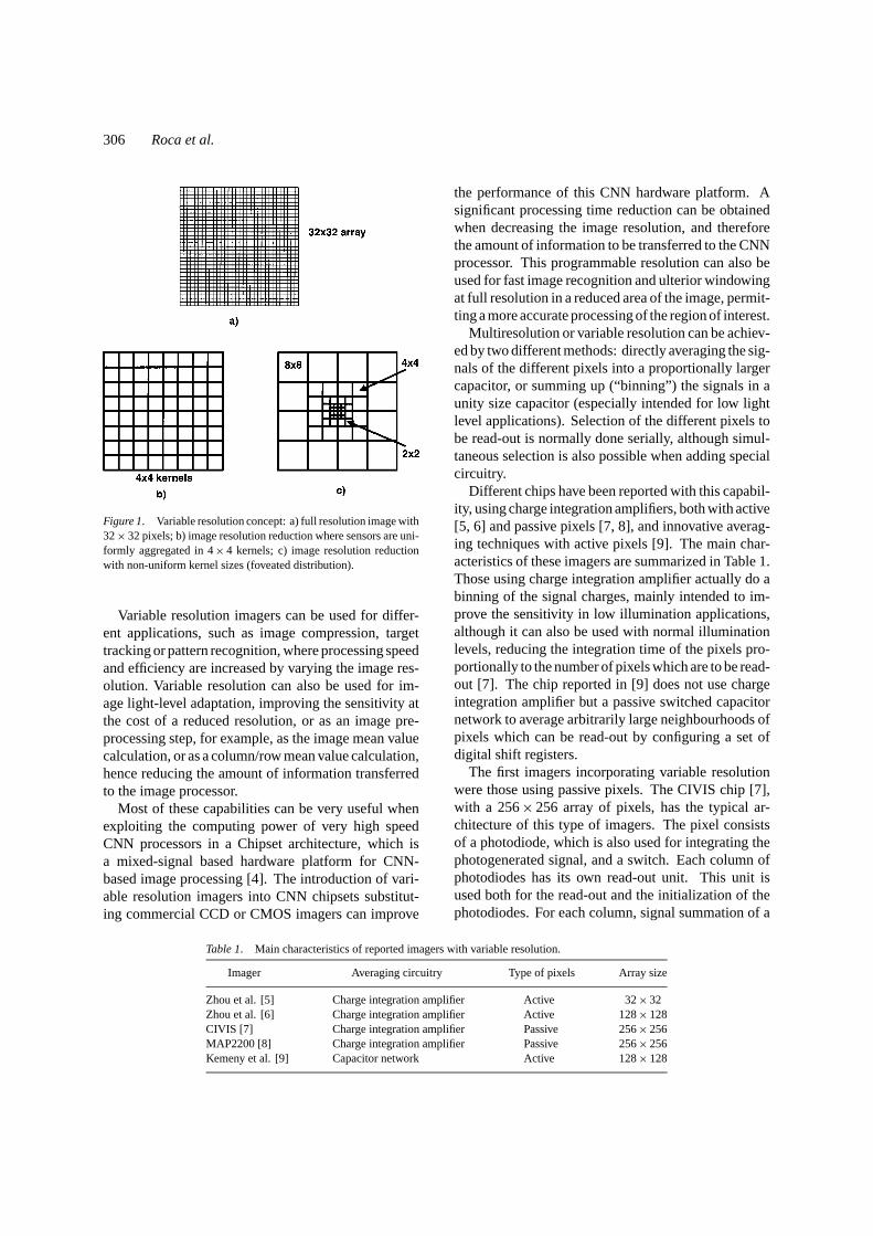
The IMAGAV-I prototype has been designed in a0.5µm, twin-well, CMOS technology, with threemetal layers, double poly and high ohmic polysiliconresistors. Only two metal layers have been used forrouting (metal1 and metal2); metal3 has been used asa light shield and also to supply the analog negativepower to the whole circuit. The technology is de-signed for 3.3 V power supply operation (Vdd= 3.3 V,Vss= 0.0 V). Independent power supply pads are pro-vided for analog, digital and electrostatic protectioncircuitry. The array size is 1.529× 1.529 mm2, andthe chip size is approximately 3.3× 5 mm2. Pixel sizeis 23.9× 23.9µm2, with a fill factor of 16%. The chipmicrophotograph can be seen in Fig. 2.
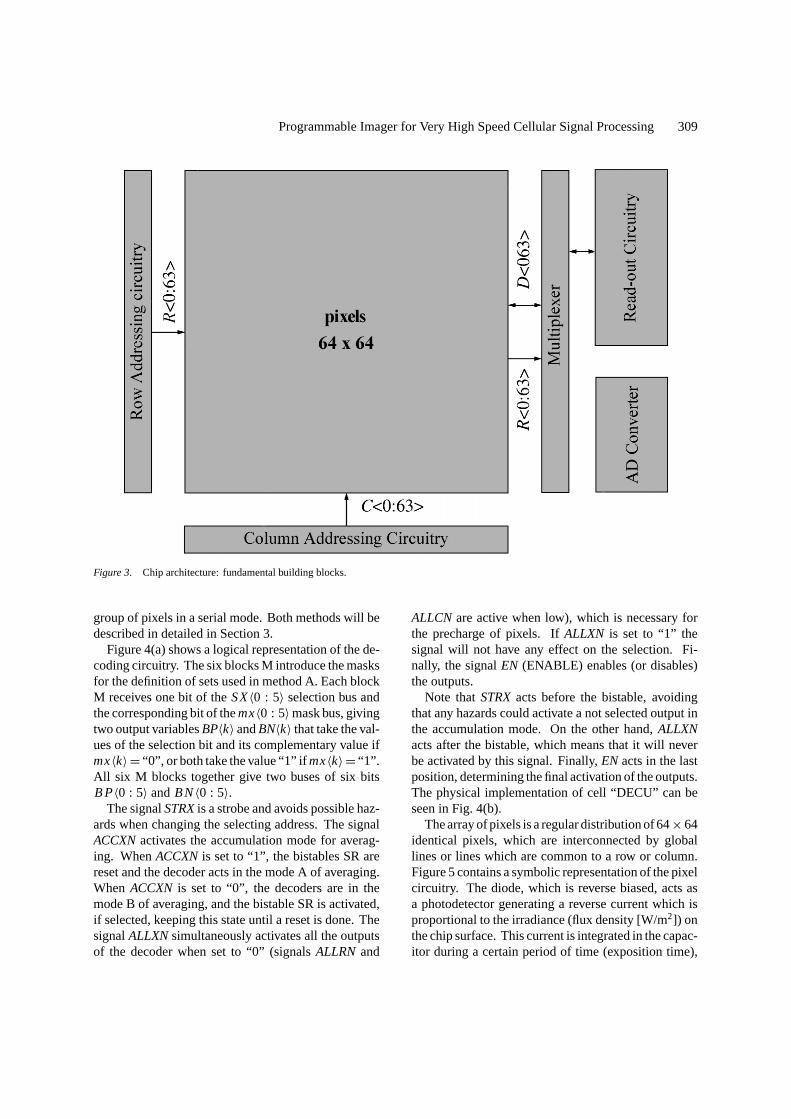
The main building blocks of the IMAGAV-I proto-type are depicted in Fig. 3. The main area is occupiedby the 64× 64 array of pixels. The row and columndecoders are placed left and down to the array. A rowmultiplexer to reduce the stray capacitance of the ar-ray and the read-out circuitry are located to the rightside of the chip. The prototype includes an 8-bits flash
308 Roca et al.
Figure 2. Chip microphotograph.
analog-to-digital (A/D) converter which can simulta-neously provide a digital value of the output signal, andoccupies the lower right part of the chip. The A/D con-verter has an independent power supply, being possibleto switch it off completely if not used.
The read-out structure includes a sole charge inte-gration amplifier with programmable gain, which is de-signed to work at a read-out frequency of up to 5 MHz.This read-out stage will contribute to reduce the fixed-pattern noise observed in other imagers where the pix-els are read-out using an amplifier per column. Thechip can perform both averaging and binning of the sig-nal charges depending on the selected feedback capac-itor of the charge integration amplifier. The read-outprocess of the group of pixels can be done simultane-ously and, up to a certain number of pixels, at the sameread-out rate.
The control of row and column selection signals (i.e.,signalsR〈0 : 63〉 andC〈0 : 63〉, see Fig. 3) is done bythe row and column addressing circuits. The circuitryused to control signalsR(i ) and that used to controlsignalsC( j ) is identical. Therefore, we will describethem simultaneously, replacing letters “R” or “ C” by
letter “X” for the purpose of making the discussiongeneral. These circuit blocks are called “decoders” be-cause that is their basic functionality, although severalother functions have been added to obtain the variableresolution.
Each decoder provides 64 output signalsX〈0 : 63〉.During the different phases of the image acquisitionprocess, these signals must all be active, all inactive,or some active and the others inactive. The selectionof all, none, or just one arbitrary signal could be doneeasily using a specific signal (e.g. ALL or NONE) anda 6 bits address bus (e.g.SX〈0 : 5〉). The definition ofan arbitrary set of signals is not as simple.
Two methods of row- or column-set definition areprovided in the prototype. First method (method A) ishighly efficient in terms of hardware and speed, but isrestricted to a certain type of sets which are thought tobe the most commonly used. Second method (methodB) is completely general, at the expense of a significantincrease in the “decoder” hardware and a substantialspeed reduction. Method A consists on defining thegroup of pixels using a 6 bits mask code. Method Bis based in “accumulating” the definition of pixels or
Programmable Imager for Very High Speed Cellular Signal Processing 309
Figure 3. Chip architecture: fundamental building blocks.
group of pixels in a serial mode. Both methods will bedescribed in detailed in Section 3.
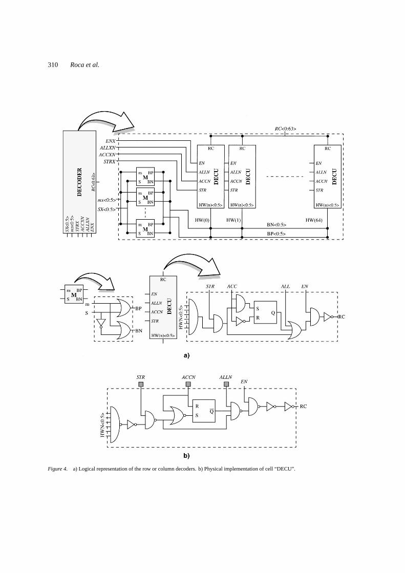
Figure 4(a) shows a logical representation of the de-coding circuitry. The six blocks M introduce the masksfor the definition of sets used in method A. Each blockM receives one bit of theSX〈0 : 5〉 selection bus andthe corresponding bit of themx〈0 : 5〉mask bus, givingtwo output variablesBP〈k〉 andBN〈k〉 that take the val-ues of the selection bit and its complementary value ifmx〈k〉= “0”, or both take the value “1” ifmx〈k〉= “1”.All six M blocks together give two buses of six bitsB P〈0 : 5〉 andBN〈0 : 5〉.
The signalSTRXis a strobe and avoids possible haz-ards when changing the selecting address. The signalACCXNactivates the accumulation mode for averag-ing. WhenACCXNis set to “1”, the bistables SR arereset and the decoder acts in the mode A of averaging.When ACCXN is set to “0”, the decoders are in themode B of averaging, and the bistable SR is activated,if selected, keeping this state until a reset is done. ThesignalALLXNsimultaneously activates all the outputsof the decoder when set to “0” (signalsALLRN and
ALLCN are active when low), which is necessary forthe precharge of pixels. IfALLXN is set to “1” thesignal will not have any effect on the selection. Fi-nally, the signalEN (ENABLE) enables (or disables)the outputs.
Note thatSTRXacts before the bistable, avoidingthat any hazards could activate a not selected output inthe accumulation mode. On the other hand,ALLXNacts after the bistable, which means that it will neverbe activated by this signal. Finally,EN acts in the lastposition, determining the final activation of the outputs.The physical implementation of cell “DECU” can beseen in Fig. 4(b).
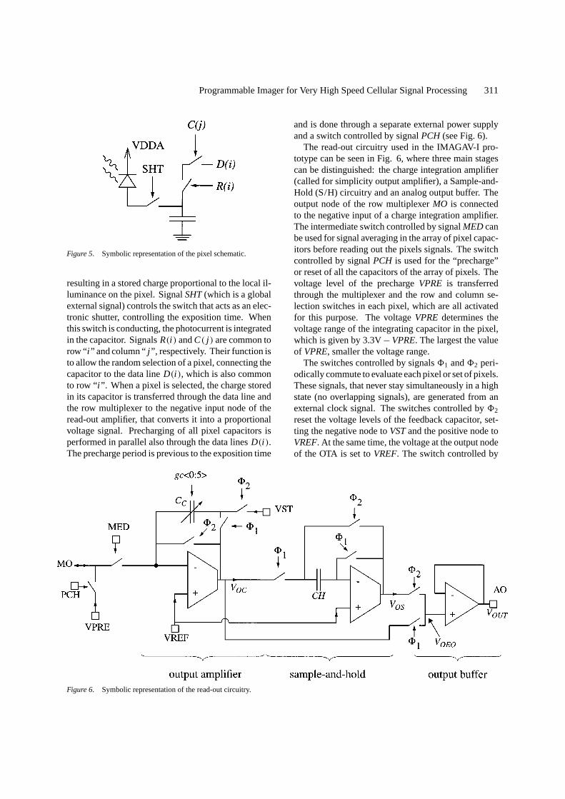
The array of pixels is a regular distribution of 64× 64identical pixels, which are interconnected by globallines or lines which are common to a row or column.Figure 5 contains a symbolic representation of the pixelcircuitry. The diode, which is reverse biased, acts asa photodetector generating a reverse current which isproportional to the irradiance (flux density [W/m2]) onthe chip surface. This current is integrated in the capac-itor during a certain period of time (exposition time),
310 Roca et al.
Figure 4. a) Logical representation of the row or column decoders. b) Physical implementation of cell “DECU”.
Programmable Imager for Very High Speed Cellular Signal Processing 311
Figure 5. Symbolic representation of the pixel schematic.
resulting in a stored charge proportional to the local il-luminance on the pixel. SignalSHT(which is a globalexternal signal) controls the switch that acts as an elec-tronic shutter, controlling the exposition time. Whenthis switch is conducting, the photocurrent is integratedin the capacitor. SignalsR(i ) andC( j ) are common torow “i ” and column “j ”, respectively. Their function isto allow the random selection of a pixel, connecting thecapacitor to the data lineD(i ), which is also commonto row “i ”. When a pixel is selected, the charge storedin its capacitor is transferred through the data line andthe row multiplexer to the negative input node of theread-out amplifier, that converts it into a proportionalvoltage signal. Precharging of all pixel capacitors isperformed in parallel also through the data linesD(i ).The precharge period is previous to the exposition time
Figure 6. Symbolic representation of the read-out circuitry.
and is done through a separate external power supplyand a switch controlled by signalPCH (see Fig. 6).
The read-out circuitry used in the IMAGAV-I pro-totype can be seen in Fig. 6, where three main stagescan be distinguished: the charge integration amplifier(called for simplicity output amplifier), a Sample-and-Hold (S/H) circuitry and an analog output buffer. Theoutput node of the row multiplexerMO is connectedto the negative input of a charge integration amplifier.The intermediate switch controlled by signalMED canbe used for signal averaging in the array of pixel capac-itors before reading out the pixels signals. The switchcontrolled by signalPCH is used for the “precharge”or reset of all the capacitors of the array of pixels. Thevoltage level of the prechargeVPRE is transferredthrough the multiplexer and the row and column se-lection switches in each pixel, which are all activatedfor this purpose. The voltageVPREdetermines thevoltage range of the integrating capacitor in the pixel,which is given by 3.3V−VPRE. The largest the valueof VPRE, smaller the voltage range.
The switches controlled by signals81 and82 peri-odically commute to evaluate each pixel or set of pixels.These signals, that never stay simultaneously in a highstate (no overlapping signals), are generated from anexternal clock signal. The switches controlled by82
reset the voltage levels of the feedback capacitor, set-ting the negative node toVSTand the positive node toVREF. At the same time, the voltage at the output nodeof the OTA is set toVREF. The switch controlled by
312 Roca et al.
81 connects the output node of the OTA to the negativenode of the feedback capacitor. Signal81 is in phasewith the selection of rows and columns, and is duringthis period when the read-out process of one pixel or setof pixels is done. During the reading period, the OTAoutput voltage will decrease since all the charge storedin the integration capacitor of the pixel or set of pixelshas been transferred to the feedback capacitor. At thismoment the voltage level will stabilize at a value givenby
VOUT = VST− 1Q
CC
= VST− CPIX
CC(VREF− (VPRE−1VPIX)) (1)
where1VPIX is the change in voltage level at the topplate of the integration capacitor in a pixel due to thecharge photogenerated by the diode. As it can be seen,voltageVSTis the reference level that determines theoutput range of the output amplifier, taking a maximumvalue of 3.3 V. The minimum value ofVREFis 0.7 V.Normally, VREFandVPREwill take the same valueand expression (1) can be written as
VOUT = VST− CPIX
CC1VPIX (2)
The feedback capacitorCC is formed by an array ofcapacitors which is binary programmable by a 6 bitsword externally controlled by busgc〈0 : 5〉 (see Fig. 6).The capacitor can take values from 1 to 63 times theunity capacitoruc, which has a value approximatelyequal to that of the integration capacitor in the pixel(0.4 pF). This programmability allows to attenuate theoutput value when voltage saturation is observed. Thiswill be necessary for the average processes, but usuallyit will be equal to 1 uc. Pixel binning is also possiblein low light illumination conditions by simply settinga unity capacitor as feedback capacitor and simultane-ously or serially selecting the different pixels withoutresetting the amplifier.
The output value of the output amplifier is sampled atthe end of each reading period and held by the Sample-and-Hold circuit during the reset period of the imager,in such a way that the analog output buffer transfers thisvoltage to a pad which can be accessed from the outsideof the chip without being affected by the reset of theoutput amplifier. The Sample-and-Hold circuit that hasbeen used presents the advantage of not being sensibleto the offset of the OTA used. The switches controlled
by the signal81, on the one hand, set the output of theOTA atVREF, resetting the output voltageVOS, and onthe other hand, connect the output voltage of the outputamplifier VOC to the capacitorCH. The voltage at thecapacitor changes withVOC, until it arrives to the finalstabilized value. The switch controlled by the signal82 connects the OTA output node to the capacitorCH,setting the voltage at the output to the same level ofthe capacitor node (which corresponds to the voltagesignal of a pixel), and holding it at the output of the S/Hduring this period. The value ofVREFis the same asfor the output amplifier. Actually, both nodes areinternally connected and accessible from the outsidethrough a unique pad.
The read-out stage is designed to operate at a fre-quency of 5 MHz when working at full resolution (read-ing out 1 pixel at a time). Although the prototype hasnot been completely tested yet, first results obtainedwhen reading out at 5 MHz through the analog outputare shown in Fig. 7, where the same image has beentaken at two different resolutions: 64× 64 pixels and32× 32 pixels. As expected, it is observed that, appar-ently, both images are free of fixed-pattern noise. Moretests are presently undergoing to extend these resultsand completely characterize the IMAGAV-1 prototype,including the use of on-chip A/D converter to directlyobtained the digital output signal.
The main difference of the IMAGAV-I prototypewith respect to other imagers with variable resolution isthat, when increasing the number of pixels to be read-out, the read-out rate is kept constant up to a largenumber of pixels. The maximum number of pixels thatcan be read is mainly determined by the programmablefeedback capacitor of the output amplifier. In our case,and since the pixel array is of 64× 64, we decided tolimit this number to 64 pixels (8× 8 kernels, or one col-umn or row). However, this number could be increasedby simply enlarging the capacitor array and adding abit (or more) to the control busgc〈0 : 5〉.
3. Averaging Modes
As already mentioned before, there exists two meth-ods of row- or column-set definition which determinethe type of averaging operation that can be performed.Method A consists on defining the group of pixels usinga 6 bits mask code. Method B is based in accumulat-ing the definition of pixels or group of pixels in a serialmode.
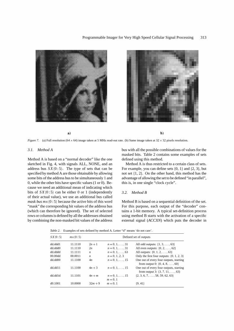
Programmable Imager for Very High Speed Cellular Signal Processing 313
Figure 7. (a) Full resolution (64× 64) image taken at 5 MHz read-out rate. (b) Same image taken at 32× 32 pixels resolution.
3.1. Method A
Method A is based on a “normal decoder” like the onesketched in Fig. 4, with signals ALL, NONE, and anaddress busSX〈0 : 5〉. The type of sets that can bespecified by method A are those obtainable by allowingsome bits of the address bus to be simultaneously 1 and0, while the other bits have specific values (1 or 0). Be-cause we need an additional mean of indicating whichbits of SX〈0 : 5〉 can be either 0 or 1 (independentlyof their actual value), we use an additional bus calledmask bus mx〈0 : 5〉 because the active bits of this word“mask” the corresponding bit values of the address bus(which can therefore be ignored). The set of selectedrows or columns is defined by all the addresses obtainedby combining the non-masked bit values of the address
Table 2. Examples of sets defined by method A. Letter “d” means ‘do not care’.
SX〈0 : 5〉 mx〈0 : 5〉 Defined set of outputs
dd.ddd1 11.1110 2n+ 1 n= 0, 1, . . . ,31 All odd outputs:{1, 3, . . . ,63}dd.ddd0 11.1110 2n n= 0, 1, . . . ,31 All even outputs:{0, 2, . . . ,62}dd.dddd 11.1111 n n= 0, 1, . . . ,63 All outputs:{0, 1, 2, . . . ,63}00.00dd 00.0011 n n= 0, 1, 2, 3 Only the first four outputs:{0, 1, 2, 3}dd.dd00 11.1100 4n n= 0, 1, . . . ,15 One out of every four outputs, starting
from output 0:{0, 4, 8, . . . ,60}dd.dd11 11.1100 4n+ 3 n= 0, 1, . . . ,15 One out of every four outputs, starting
from output 3:{3, 7, 11, . . . ,63}dd.dd1d 11.1101 4n+m n= 0, 1, . . . ,15 {2, 3, 6, 7, . . . ,58, 59, 62, 63}
m= 0, 1d0.1001 10.0000 32m+ 9 m= 0, 1 {9, 41}
bus with all the possible combinations of values for themasked bits. Table 2 contains some examples of setsdefined using this method.
Method A is thus restricted to a certain class of sets.For example, you can define sets{0, 1} and{2, 3}, butnot set{1, 2}. On the other hand, this method has theadvantage of allowing the set to be defined “in parallel”,this is, in one single “clock cycle”.
3.2. Method B
Method B is based on a sequential definition of the set.For this purpose, each output of the “decoder” con-tains a 1-bit memory. A typical set-definition processusing method B starts with the activation of a specificexternal signal (ACCXN) which puts the decoder in
314 Roca et al.
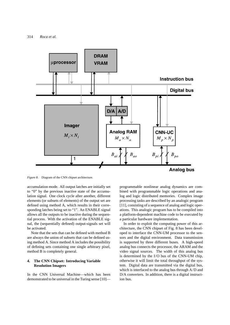
Figure 8. Diagram of the CNN chipset architecture.
accumulation mode. All output latches are initially setto “0” by the previous inactive state of the accumu-lation signal. One clock cycle after another, differentelements (or subsets of elements) of the output set aredefined using method A, which results in their corre-sponding latches being set to “1”. An ENABLE signalallows all the outputs to be inactive during the sequen-tial process. With the activation of the ENABLE sig-nal, the (sequentially defined) output-signals set willbe activated.
Note that the sets that can be defined with method Bare always the union of subsets that can be defined us-ing method A. Since method A includes the possibilityof defining sets containing one single arbitrary pixel,method B is completely general.
4. The CNN Chipset: Introducing VariableResolution Imagers
In the CNN Universal Machine—which has beendemonstrated to be universal in the Turing sense [10]—
programmable nonlinear analog dynamics are com-bined with programmable logic operations and ana-log and logic distributed memories. Complex imageprocessing tasks are described by an analogic program[11], consisting of a sequence of analog and logic oper-ations. This analogic program has to be compiled intoa platform-dependent machine code to be executed bya particular hardware implementation.
In order to exploit the computing power of this ar-chitecture, the CNN chipset of Fig. 8 has been devel-oped to interface the CNN-UM processor to the sen-sors and the digital environment. Data transmissionis supported by three different buses. A high-speedanalog bus connects the processor, the ARAM and thevideo signal sources. The width of this analog busis determined by the I/O bus of the CNN-UM chip,otherwise it will limit the total throughput of the sys-tem. Digital data are transmitted via the digital bus,which is interfaced to the analog bus through A/D andD/A converters. In addition, there is a digital instruct-ion bus.
Programmable Imager for Very High Speed Cellular Signal Processing 315
Assume an input image composed ofMi×Ni -pixels(Fig. 8). It has to be decomposed intoMa×Na-pixelsubsets that are temporarily stored one-by-one in theanalog RAM chip for their processing. However, pix-els in the border of thisMa×Na window will not beproperly processed unless a certain overlap between theimage fractions is allowed. Therefore,mo andno pixeloverlaps in the vertical and the horizontal direction, re-spectively, are considered. Taking this into account, astraightforward calculation shows that,
k = (Mi −mo)× (Ni − no)
(Ma −mo)× (Na − no)(3)
subimages are needed to cover the whole image. Eachof these subimages has to be captured, processed anddownloaded, thus resulting into the following total pro-cessing timeTi for the Mi × Ni input frame,
Ti = (Mi −mo)×(Ni − no)
(Ma −mo)×(Na − no)· (Tai + Tap+ Tao) (4)
whereTai , Tao and Tap are the times required to ac-quire, download and process each subimage, respec-tively. For the former two times, and assuming thatBai and Bao are the widths of the input and outputbuses of the ARAM, the following is obtained,
Tai = Ma × Na
Bai· τai
(5)
Tao = Ma × Na
Bao· τao
whereτai andτao are the times required for writing andreading, respectively, an analog register of the ARAMchip.
With regards to the processing timeTap in (4) wehave to take into account that, in the more generalcase, the processor size is smaller than the ARAMsize. Hence, the necessity arises for another multiplex-ation. Assume the size of the processor isMp× Np
and that each analogic program containsni data ac-quisition steps,nap analog processing steps,nlp logicprocessing operations, andnd data downloads. Thus,the time needed to perform the analogic algorithm oneachMa× Na subset is given by,
Tap = (Ma −mo)× (Na − no)
(Mp −mo)× (Np − no)· Tpp (6)
where,
Tpp = ni Tpi + napTpap+ nlpTplp + ndTpo, (7)
andTpap andTplp are the times required for the analogand the digital circuitry of the CNN-UM to settle andcomplete the logic operation, respectively. These pa-rameters are part of the timing specs of the CNN-UMchip. Tpi andTpo in the expression above representsI/O times which are given by,
Tpi = Mp × Np
Bpi· τpi
(8)
Tpo = Mp × Np
Bpo· τpo
whereBpi andBpo are the widths of the input and out-put buses of the CNN-UM, respectively, andτpi andτpo are the times required for updating and download-ing analog data from one cell of the CNN array—alsodefined as temporal specs of the processing chip.
Assume a frame rate ofNf frames per second. Thefollowing must be accomplished in order to process thewhole input image (Mi × Ni ) in real-time:
Ti ≤ 1
Nf(9)
Thus, from the mathematics above, the following de-sign equation can be obtained,
1
Nf≥ MaNa(Mi −mo)(Ni − no)
(Ma −mo)(Na − no)
(τai
Bai+ τao
Bao
)+ (Mi −mo)(Ni − no)
(Mp −mo)(Np − no)Tpp (10)
We find convenient to illustrate this design equationusing typical values. For instance, consider a frame rateof 40 frames per second, an input image of 512× 512pixels, an analog RAM buffer of 32× 256 registersand a CNN array of 32× 32 cells. Consider as wella 2-pixel wide overlap in both, vertical and horizon-tal, scan directions and 16-line wide I/O buses. Then,for a typical I/O time of 500 ns per memory cell, theCNN-UM chip should be capable to complete the ana-logic algorithm over eachMp× Np subimage in lessthan 26µs—well within the specs of CMOS CNN-UMchips [12, 13]. The larger the CNN processor size thefaster the system is. Besides, pipelined architecturesand some interleaving of the memory blocks can be
316 Roca et al.
used for a more relaxed constrain on the processingtime.
However, there is another way to increase the pro-cessing speed of the system, which is including animager with programmable resolution as the image ac-quisition system. With the addition of a few digitalcontrol signals, the imager resolution could be changedto adapt it to the necessities of the image scene, espe-cially when no small details are to be analysed. Inthis way a complete image could be transferred to aCNN-UM processor in much less time than in a com-mercial imager. If the resolution of the acquired imageis not enough for the processing algorithm, two dif-ferent solutions can be taken: increase the resolution,or, if possible, select an area of interest and re-processit in detailed (at full resolution). This last solutionwill always be the more efficient in processing time,although it would need that the CNN-UM output in-formation could be used as a feedback control signalfor the imager. This could be done by incorporatingadditional circuitry to the chipset hardware. Besidesof the variable resolution, the imager should also pro-vide random access to any pixel of the array, which isnot always possible with commercial imagers such asCCDs due to their intrinsic serial read-out structure.
The IMAGAV-1 imager is a prototype that accom-plishes the main conditions proposed above to increasethe processing speed of CNN chipsets, including ran-dom access to the different pixels. In addition, fur-ther pre-processing operations, such as column or rowaverage, are also possible and can be useful in someimage processing tasks. Its main advantage over otherimagers with variable resolution is the capability ofmaintaining the read-out rate when decreasing the res-olution, up to large kernel sizes.
Although the size of this prototype is not too large, itcan already be used with actual CNN processor arrays.A larger imager with the same capabilities would bedeveloped in the future to be incorporated with largerCNN-UM chips that are under development [13].
5. Conclusions
We have presented a programmable imager with aver-aging chip which is intended for averaging of differentgroups or sets of pixels formed byn× n kernels,n×mkernels or independent pixels of the array. This imageris a 64× 64 array which uses passive pixels that can berandomly accessed. The read-out stage includes a solecharge integration amplifier with programmable gain,
which is designed to work at a read-out frequency ofup to 5 MHz. This read-out structure reduces the fixed-pattern noise present in other imagers where the pixelsare read-out using an output amplifier per column. Thechip can perform both averaging and binning of the sig-nal charges depending on the selected feedback capac-itor of the charge integration amplifier. The read-outprocess of the group of pixels can be done simultane-ously and, up to a certain number of pixels, at the sameread-out rate.
This programmable resolution architecture is moreappropriate and efficient when implementing very highspeed Cellular Neural Network (CNN) processors in aCNN chipset. A significant processing time reductioncan be obtained when decreasing the image resolution,and therefore the number of information to be trans-ferred to the CNN processor. This programmable res-olution can also be used for fast image recognition andulterior windowing at full resolution in a reduced areaof the image, permitting a more accurate processingof the region of interest. In addition, full resolutionimages can still be obtained.
Acknowledgments
This work has been founded by NICOP Grant N68171-98-C-9004 and CICYT Grant No. TIC96-1392-C02-02.
References
1. E.R. Fossum, “CMOS image sensors: Electronic camera on achip,” Int. Electron Device Meetings, pp. 17–25, 1995.
2. H.-S. Wong, “Technology and device scaling considerationsfor CMOS imagers,”IEEE Transactions on Electron Devices,Vol. 43, No. 12, pp. 2131–2142, 1996.
3. G. Meynants, B. Dierickx, and D. Scheffer, “CMOS activepixel image sensor with CCD performance,”Proceeding SPIE,Vol. 3410, pp. 68–76, 1998.
4. T. Roska, “CNN chip set architectures and the visual mouse,”Proceedings of the 4th IEEE Int. Workshop on Cellular NeuralNetworks and their Applications, Sevilla, Spain, pp. 487–492,June 1996.
5. Z. Zhou, B. Pain, and E.R. Fossum, “Frame-transfer CMOSactive pixel sensor with pixel binning,”IEEE Transactions onElectron Devices, Vol. 44, No. 10, pp. 1764–1768, 1997.
6. Z. Zhou, B. Pain, and E.R. Fossum, “A CMOS imager with on-chip variable resolution for light-adaptive imaging,”Proceed-ing of the IEEE International Solid-State Circuits Conference,pp. 174–175, 1998.
7. N. Ricquier, I. Debusschere, B. Dierickx, A. Alaerts, J.Vlummens, and C. Claeys, “The CIVIS sensor: a flexiblesmart imager with programmable resolution,”Proceeding SPIE,Vol. 2172, pp. 2–10, 1994.
Programmable Imager for Very High Speed Cellular Signal Processing 317
8. C. Jansson, P. Ingelhag, C. Svensson, and R. Forchheimer, “Anaddressable 256× 256 photodiode image sensor array with an8-bit digital output,”Analog Integrated Circuits and Signal Pro-cessing, Vol. 4, pp. 37–49, 1993.
9. S.E. Kemeny, R. Panicacci, B. Pain, L. Matthies, and E.R.Fossum, “Multiresolution image sensor,”IEEE Transactionson Circuits and Systems for Video Technology, Vol. 7, No. 4,pp. 575–583, 1997.
10. K.R. Crounse and L.O. Chua, “The CNN universal machine is asuniversal as a Turing machine,”IEEE Transactions on Circuitsand Systems I: Fundamental Theory and Applications, Vol. 43,No. 4, pp. 353–355, April 1996.
11. T. Roska and L.O. Chua, and A. Zarandy, “Language, com-piler and operating system for the CNN supercomputer,” ReportUCB/ERL M93/34, University of California, Berkeley, 1993.
12. S. Espejo, A. Rodr´ıguez-Vazquez, and R. Dom´ınguez-Castro,“Smart-pixel cellular neural networks in analog current-modeCMOS technology,” IEEE Journal of Solid-State Circuits,Vol. 29, pp. 895–905, IEEE Aug. 1994.
13. S. Espejo, R. Dom´ınguez-Castro, G. Li˜nan, and A. Rodr´ıguez-Vazquez, “64× 64 CNN Universal Chip with Analog and Dig-ital I/O,” IEEE 1998 Int. Conf. on Electronic Circuits and Sys-tems, Lisbon, Sep. 1998.
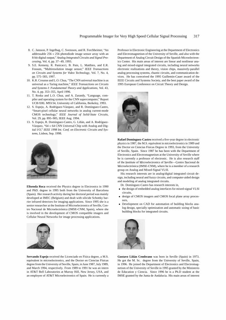
Elisenda Rocareceived the Physics degree in Electronics in 1990and PhD. degree in 1995 both from the University of Barcelona(Spain). Her research activity during her doctoral period was mainlydeveloped at IMEC (Belgium) and dealt with silicide Schottky bar-rier infrared detectors for imaging applications. Since 1995 she is asenior researcher at the Institute of Microelectronics of Seville, Cen-tro Nacional de Microelectr´onica (IMSE-CNM, Spain), where sheis involved in the development of CMOS compatible imagers andCellular Neural Networks for image processing applications.
Servando Espejoreceived the Licenciado en F´ısica degree, a M.S.equivalent in microelectronics, and the Doctor en Ciencias F´ısicasdegree from the University of Seville, Spain, in June 1987, July 1989,and March 1994, respectively. From 1989 to 1991 he was an internin AT&T Bell Laboratories at Murray Hill, New Jersey, USA, andan employee of AT&T Microelectronics of Spain. He is currently a
Professor in Electronic Engineering at the Department of Electronicsand Electromagnetism of the University of Seville, and also with theDepartment of Analog Circuit Design of the Spanish Microelectron-ics Center. His main areas of interest are linear and nonlinear ana-log and mixed-signal integrated circuits, including neural networkselectronic realizations and theory, vision chips, massively-parallelanalog processing systems, chaotic circuits, and communication de-vices. He has coreceived the 1995 Guillemin-Cauer award of theIEEE Circuits and Systems Society, and the best paper award of the1995 European Conference on Circuit Theory and Design.
Rafael Domınguez-Castroreceived a five-year degree in electronicphysics in 1987, the M.S. equivalent in microelectronics in 1989 andthe Doctor en Ciencias Fisicas Degree in 1993, from the Universityof Seville, Spain. Since 1987 he has been with the Department ofElectronics and Electromagnetism at the University of Seville wherehe is currently a professor of electronic. He is also research staffof the I
¯nstitute of M
¯icroelectronics of S
¯eville—C
¯entro N
¯acional de
M¯
icroelectronica (IMSE-CNM), where he is a member of a researchgroup on Analog and Mixed-Signal VLSI.
His research interests are in analog/digital integrated circuit de-sign, including neural and fuzzy circuits, and computer-aided designand modeling of analog integrated circuits.
Dr. Domınguez-Castro has research interests in,• the design of embedded analog interfaces for mixed-signal VLSI
circuits,• design of CMOS imagers and CMOS focal plane array proces-
sors,• Development on CAD for automation of building blocks ana-
log design, specially optimization and automatic sizing of basicbuilding blocks for integrated circuits.
Gustavo Linan Cembrano was born in Seville (Spain) in 1973.He got the M. Sc. degree from the University of Seville, Spain,in 1996. He joined the Department of Electronics and Electromag-netism of the University of Seville in 1995 granted by the Ministeriode Education y Ciencia. Since 1996 he is a Ph.D student at theIMSE granted by the Junta de Andalucia. His main areas of interest
318 Roca et al.
are linear and nonlinear mixed-signal integrated circuits theory anddesign focussing in Cellular Neural Networks theory and electronicimplementations.
Angel Rodrıguez-Vazquez,IEEE Fellow,is a Professor of Electron-ics at the Department of Electronics and Electromagnetism (Uni-versity of Seville). He is also a member of the research staff ofthe I
¯nstitute of M
¯icroelectronics of S
¯eville—C
¯entro N
¯acional de
M¯
icroelectronica (IMSE-CNM)— where he is heading a researchgroup on Analog and Mixed-Signal VLSI. His research interests arein the design of analog interfaces for mixed-signal VLSI circuits,CMOS imagers and vision chips, neuro-fuzzy controllers, symbolicanalysis of analog integrated circuits and optimization of analog in-tegrated circuits.
Dr. Rodrıguez-Vazquez served as an Associate Editor of the IEEETransactions on Circuits and Systems-I from 1993 to 1995, as GuestEditor of the IEEE TCAS-I special issue on “Low-Volt-age and Low-Power Analog and Mixed-Signal Circuits and Systems” (1995), asGuest Editor of the IEEE TCAS-II special issue on “Advances inNonlinear Electronic Circuits” (1999), and as chair of the IEEE-CAS Analog Signal Processing Committee (1996).
He was co-recipient of the 1995 Guillemin-Cauer award of theIEEE Circuits and Systems Society, and the best paper award of the1995 European Conference on Circuit Theory and Design. In 1992he received also the young scientist award of the Seville Academy ofScience. In 1996 he was elected to the degree of Fellow of the IEEEfor “contributions to the design and applications of analog/digitalnonlinear ICs.”