a 10 dbm-25 dbm, 0.363 mm2 two stage 130 nm rf cmos power amplifier
TRANSCRIPT
International Journal of VLSI design & Communication Systems (VLSICS) Vol.4, No.5, October 2013
DOI : 10.5121/vlsic.2013.4509 107
A 10 dBm-25 dBm, 0.363 mm2 TWO STAGE
130 nm RF CMOS POWER AMPLIFIER
Shridhar R. Sahu1 and Dr. A. Y. Deshmukh
2
1Research Scholar, Department of Electronics Engineering, G. H. Raisoni College of
Engineering, Nagpur, India 2Professor, Department of Electronics Engineering, G. H. Raisoni College of
Engineering, Nagpur, India
Abstract
This paper proposes a 2.4 GHz RF CMOS Power amplifier and variation in its main performance
parameters i.e, output power, S-parameters and power added efficiency with respect to change in supply
voltage and size of the power stage transistor. The supply voltage was varied form 1 V to 5 V and the range
of output power at 1dB compression point was found to be from 10.684 dBm to 25.08 dBm respectively.
The range of PAE is 16.65 % to 48.46 %. The width of the power stage transistor was varied from 150 µm
to 500 µm to achieve output power of range 15.47 dBm to 20.338 dBm. The range of PAE obtained here is
29.085 % to 45.439 %. The total dimension of the layout comes out to be 0.714 * 0.508 mm2.
Keywords
RF CMOS, PAE, Output Power, S-parameters, Matching Networks
1. INTRODUCTION
CMOS RFICs are Radio Frequency Integrated circuits in CMOS technology operated in radio
frequency range. RF Power Amplifiers are part of the transmitter front-end used to amplify the
input power to be transmitted [1][3].
The main performance parameters for the power amplifier are the level of output power it can
achieve, depending on the targeted application, linearity, and efficiency. The two basic definitions
for the efficiency of the power amplifier are drain efficiency (DE) which is the ratio between the
RF output power to the dc power dissipated, and the power added efficiency (PAE) which is the
ratio between the difference of the RF output power and the RF input power to the total dc power
of the circuit. The PAE is a more practical measure as it is responsible for the power gain of the
amplifier [1].
International Journal of VLSI design & Communication Systems (VLSICS) Vol.4, No.5, October 2013
108
PP
dc
RFoutDE
)(=
(2)
RFICs are fabricated using CMOS, GaAs Hetero-Junction Bipolar Transistor (HBT), SiGe
BiCMOS, , GaN High Electron Mobility Transistor (HEMT) technologies. Existing power
amplifiers mostly use GaAs (Gallium Arsenide) or GaN (Gallium Nitride) for high output power.
But it also leads to high power dissipation, large chip area and more cost. The GaAs technology
provides high output power at high frequency, but it is quite expensive and the uniformity of the
device structure may be affected due to process variations [6]. The GaN process also operates at
higher frequencies and deals with high power capacity but due to wide band gap materials used
more voltage supply is needed for operation which in turn leads to high power dissipation [7].
CMOS power amplifiers can also be operated at high frequencies and by using some techniques
output power can be increased. CMOS power amplifiers show more linearity as compared to
GaAs and GaN technologies. As CMOS can operate on low power supplies there is drastic
decrease in overall power dissipation of the circuit and hence better PAE can be expected. CMOS
power amplifiers are cost effective and use minimum chip area for fabrication.
The main objective behind this paper is to design a CMOS Power Amplifier for 2.4 GHz WLAN
application and observe change in its important parameters such as s-parameters, output power,
power added efficiency with change in supply voltage and size of the power stage transistor. The
tool used for designing this circuit is ADS (Advanced Design System) tool of Agilent Systems.
This circuit is designed in RFCMOS 130 nm technology. The layout of this paper is follows:
Initially this paper deals with the schematic of the CMOS power amplifier, then the simulation
results obtained by varying supply voltage and size of second stage transistor. Layout of the
designed circuit is drawn in Tanner Tool. Finally, conclusions are drawn out after observing the
simulation results.
2. SCHEMATIC
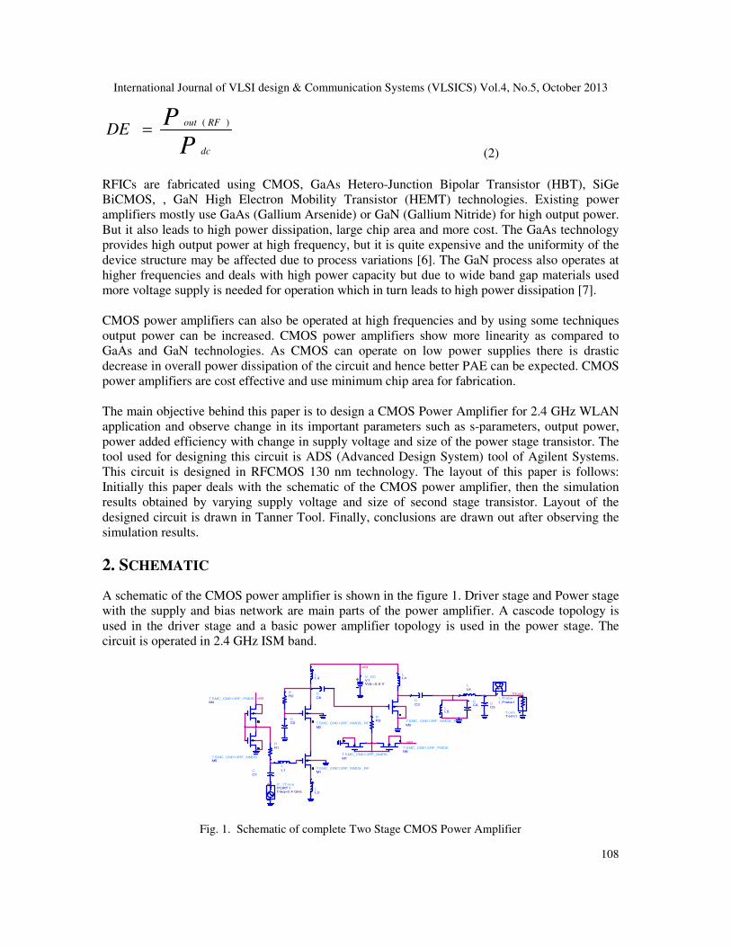
A schematic of the CMOS power amplifier is shown in the figure 1. Driver stage and Power stage
with the supply and bias network are main parts of the power amplifier. A cascode topology is
used in the driver stage and a basic power amplifier topology is used in the power stage. The
circuit is operated in 2.4 GHz ISM band.
Fig. 1. Schematic of complete Two Stage CMOS Power Amplifier
vdd
Vload
vdd
vdd
TermTerm1
TSMC_CM013RF_NMOS_RF
M3
TSMC_CM013RF_NMOS
M7
TSMC_CM013RF_PMOSM6
TSMC_CM013RF_NMOSM5
TSMC_CM013RF_PMOSM4
TSMC_CM013RF_NMOS_RF
M2
TSMC_CM013RF_NMOS_RFM1
C
C6 I_Probe
I_Probe1CC5
V_DCV1Vdc=2.5 V
LL4
C
C3CC4
RR3
LL5
L
L6
LL3
LL2
RR2
R
R1
CC2
P_1TonePORT1Freq=2.4 GHz
C
C1
L
L1
International Journal of VLSI design & Communication Systems (VLSICS) Vol.4, No.5, October 2013
109
A cascode topology is implemented in the first stage. The transistor M1 is the main amplifying
device of this stage and transistor M2 is cascaded with M1. An inductor of a large value is
connected between the drain of M2 and VDD which opposes the change in current and the
cascaded transistor is to prevent large flow of drain current through M1. The transistor M2 is
biased in saturation. Transistor M1 is biased by a MOSFET only bias circuit whose output is 0.5
Volts to operate in triode region. The transistor was first analyzed with different biasing voltages
and found to be operating better at 0.5 V in similar conditions. An input matching network is
connected to the driver stage i.e., the input stage for input impedance matching. For this matching
purpose gate inductance Lg (L1) and source inductance Ls (L2) are used. The values of these
inductances and the size of the transistors are such selected that the operation of the circuit is
tuned to the resonance frequency of 2.4 GHz. The gate length of the transistors is fixed at 130nm
and the width of gate is varied. The output power of this topology is not as high as the power
stage but the isolation provided between output and input is very high. Also the dc power
consumed by this circuit is far less than the power stage circuit. The dc current through this stage
is 6.31 mA at 2.5 V.
The second stage is mainly responsible for power amplification considering the overall circuit.
The size of the transistor used in this stage is large as compared to the size the transistors used in
the driver stage. A big fat inductance is connected between the dc supply and the drain of the
transistor M3. The output of the driver stage is fed to the gate of the transistor M3 through the
capacitor C6. The dc current here is controlled by varying the size of the transistor. The
amplification of the signal also depends on the bias voltage supply. Bias voltage is 0.75 V. Output
matching network is connected at the output side for output impedance matching. Here, a LC tank
circuit is designed for matching purpose and to tune the circuit to its operating frequency, so that
the output return loss is better at resonance frequency. The total dc current of this stage comes out
to be 83.5 mA at 2.5 V.
3. SIMULATION RESULTS
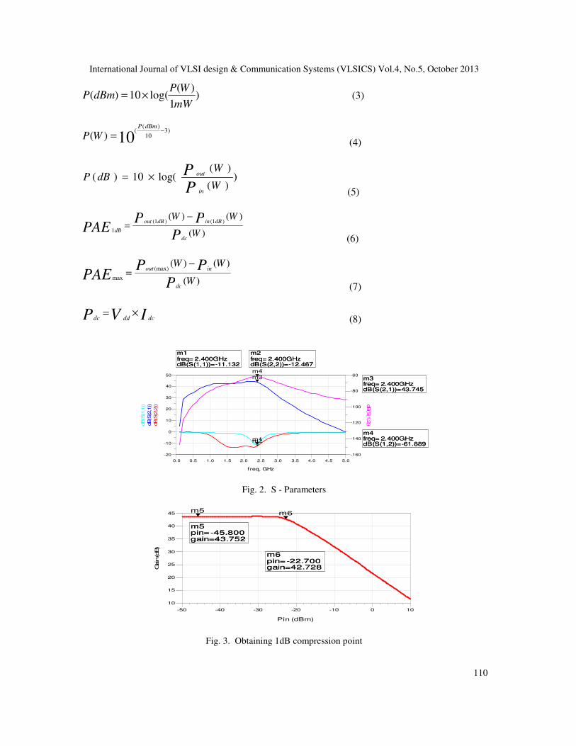
S – Parameters are an important part of Power amplifiers. There are four s-parameters essential to
observe after designing a power amplifier. They are input return loss S(1,1), output return loss
S(2,2), gain S(2,1) and isolation loss S(1,2).
Power calculations are carried out at 1dB compression point of the gain of the circuit. As shown
in the figure 3, graph of gain in dB is plotted v/s input power in dBm. According to the figure
1dB compression point is obtained at -22.7 dBm of input power. Output power is observed at the
same input power which comes out to be 20.028 dBm. This output power is known as output
power at 1dB compression point. The maximum output power delivered by this circuit is 22.002
dBm. The unit used for power calculations of a power amplifier is dBm instead of watts. The
conversion of watts to dBm and dBm to watts is given as in equation (3). The equation for power
gain is given as in equation (5).
Power added efficiency; the factor by which the power amplifiers are analyzed is the deciding
parameter between different types of power amplifiers. This CMOS power amplifier operating at
2.4 GHz with a main supply of 2.5 V gives PAE of 44.669 % at 1dB compression point. The
maximum PAE achieved by the circuit is 70.196 %. These values can be observed in figure 8
where on left y axis pout is plotted and on right y axis PAE is plotted. The equations for the same
are given in equation 6, 7 and 8.
International Journal of VLSI design & Communication Systems (VLSICS) Vol.4, No.5, October 2013
110
)1
)(log(10)(
mW
WPdBmP ×= (3)
10)3
10
)((
)(−
=
dBmP
WP (4)
))(
)(log(10)(
W
WdBP
PP
in
out×=
(5)
)(
)()()1()1(
1 W
WW
P
PPPAE
dc
dBindBout
dB
−
=
(6)
)(
)()((max)
max W
WW
P
PPPAE
dc
inout−
=
(7)
IVP dcdddc×=
(8)
Fig. 2. S - Parameters
Fig. 3. Obtaining 1dB compression point
m1freq=dB(S(1,1))=-11.132
2.400GHzm2freq=dB(S(2,2))=-12.467
2.400GHz
m3freq=dB(S(2,1))=43.745
2.400GHz
m4freq=dB(S(1,2))=-61.889
2.400GHz
0.5 1.0 1.5 2.0 2.5 3.0 3.5 4.0 4.50.0 5.0
-10
0
10
20
30
40
-20
50
-140
-120
-100
-80
-160
-60
freq, GHz
dB(S
(2,2
))
m2
dB(S
(2,1
))
m3
dB(S
(1,2
))
m4
dB(S
(1,1
))
m1
m1freq=dB(S(1,1))=-11.132
2.400GHzm2freq=dB(S(2,2))=-12.467
2.400GHz
m3freq=dB(S(2,1))=43.745
2.400GHz
m4freq=dB(S(1,2))=-61.889
2.400GHz
m5pin=gain=43.752
-45.800
m6pin=gain=42.728
-22.700
-40 -30 -20 -10 0-50 10
15
20
25
30
35
40
10
45
Pin (dBm)
Gain (dB)
m5 m6
m5pin=gain=43.752
-45.800
m6pin=gain=42.728
-22.700

International Journal of VLSI design & Communication Systems (VLSICS) Vol.4, No.5, October 2013
111
Fig. 4. Output Power and Power Added Effciency
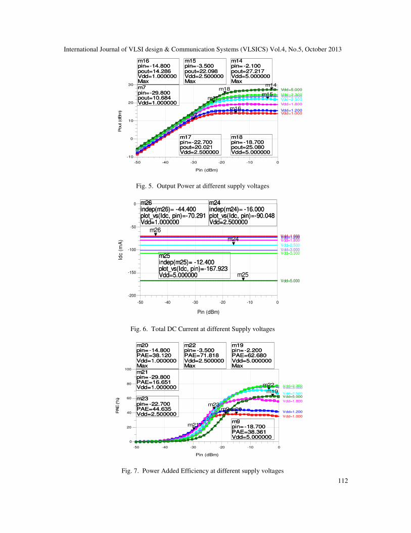
3.1 Variation in Output Power, S-Parameters and PAE with change in Supply
Voltage
The supply voltage was varied from 1 V to 5 V. The operating frequency was kept constant i.e,
2.4 GHz. The values of s-parameters, output power, PAE achieved are tabulated in table 1. The
range of output power at 1dB compression point observed is 10.684 dBm to 25.08 dBm. The
range of maximum output power is 14.286 dBm to 27.217 dBm. Power added efficiency at 1dB
compression point is calculated to be 16.65 % at 1 V to 48.46 % at 3.3 V. Maximum PAE is
38.12 % at 1 V to 77.407 % at 3.3 V. The overall DC current observed here is 70.23 mA at 1 V to
168 mA at 5 V. These results can also be observed in figures 5, 6, & 7.
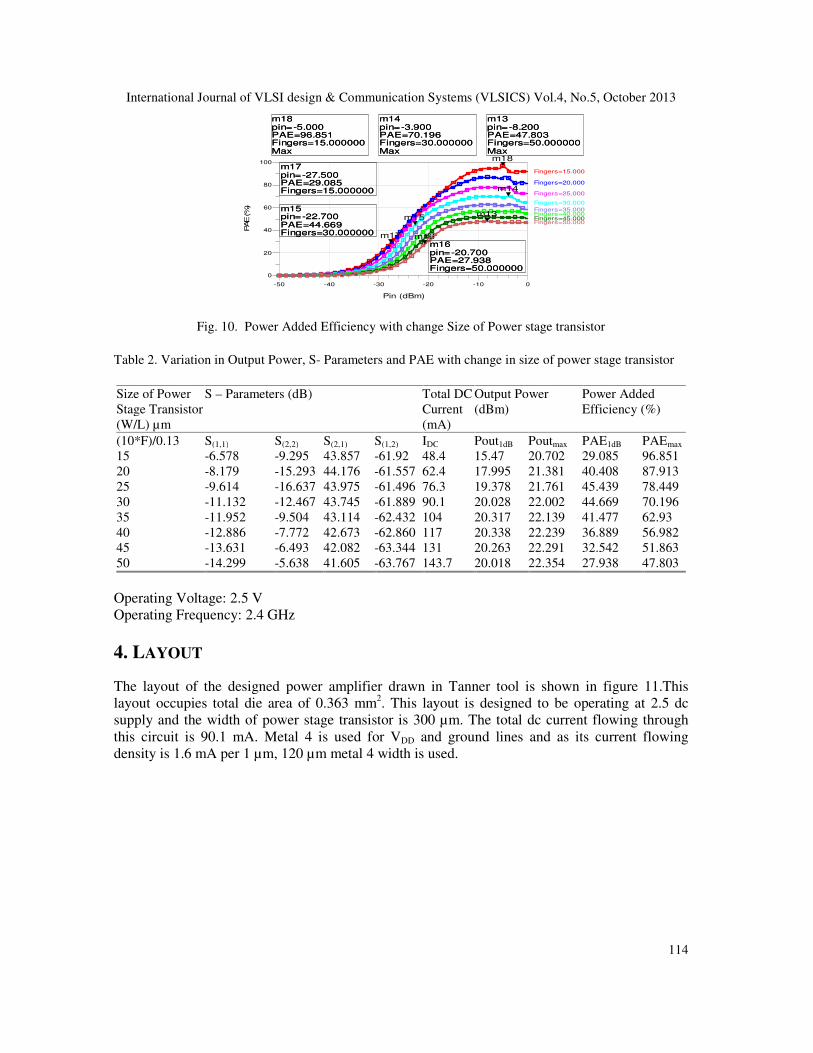
3.2 Variation in Output Power, S- parameters and PAE with change in Size of
Power stage Transistor
Initially the width of the second stage transistor was 300 µm, i.e, 30 gate fingers with 10 µm
width of single gate finger. The number of gate fingers was varied to change the size of the
transistor. The gate fingers were varied from 15 to 50 numbers making the width effectively 150
µm to 500 µm. The results obtained are tabulated in table 2. The operating voltage and operating
frequency were kept constant at 2.5 V and 2.4 GHz respectively. The number of gate fingers here
is denoted as F. The range of output power at 1dB compression point observed is 15.47 dBm to
20.338 dBm. The range of maximum output power is 20.702 dBm to 22.354 dBm. Power added
efficiency at 1dB compression point is calculated to be 29.085 % at 150 µm gate width to 45.439
% at 25 um gate width. The overall DC current observed here is 48.4 mA at 15 gate fingers to
143.7 mA at 50 gate fingers. These results can also be observed in figures 8, 9, & 10.
m7pin=pout=20.028
-22.700
m8pin=pout=22.002Max
-3.900
m9pin=PAE=44.669
-22.700
m10pin=PAE=70.196Max
-3.900
-40 -30 -20 -10 0-50 10
-5
0
5
10
15
20
-10
25
20
40
60
80
0
100
Pin (dBm)
Pout (d
Bm
)
m7m8
PAE (%
)
m9
m10
m7pin=pout=20.028
-22.700
m8pin=pout=22.002Max
-3.900
m9pin=PAE=44.669
-22.700
m10pin=PAE=70.196Max
-3.900
International Journal of VLSI design & Communication Systems (VLSICS) Vol.4, No.5, October 2013
112
Fig. 5. Output Power at different supply voltages
Fig. 6. Total DC Current at different Supply voltages
Fig. 7. Power Added Efficiency at different supply voltages
m7pin=pout=10.684Vdd=1.000000
-29.800
m14pin=pout=27.217Vdd=5.000000Max
-2.100m15pin=pout=22.098Vdd=2.500000Max
-3.500m16pin=pout=14.286Vdd=1.000000Max
-14.800
m17pin=pout=20.021Vdd=2.500000
-22.700m18pin=pout=25.080Vdd=5.000000
-18.700
-40 -30 -20 -10-50 0
0
10
20
-10
30
Vdd=1.000Vdd=1.200
Vdd=1.800
Vdd=2.500Vdd=3.000Vdd=3.300
Vdd=5.000
Pin (dBm)
Pout (d
Bm
)m7
m14
m15
m16
m17
m18m7pin=pout=10.684Vdd=1.000000
-29.800
m14pin=pout=27.217Vdd=5.000000Max
-2.100m15pin=pout=22.098Vdd=2.500000Max
-3.500m16pin=pout=14.286Vdd=1.000000Max
-14.800
m17pin=pout=20.021Vdd=2.500000
-22.700m18pin=pout=25.080Vdd=5.000000
-18.700
m24indep(m24)=plot_vs(Idc, pin)=-90.048Vdd=2.500000
-16.000
m25indep(m25)=plot_vs(Idc, pin)=-167.923Vdd=5.000000
-12.400
m26indep(m26)=plot_vs(Idc, pin)=-70.291Vdd=1.000000
-44.400
-40 -30 -20 -10-50 0
-150
-100
-50
-200
0
Vdd=1.000Vdd=1.200Vdd=1.800Vdd=2.500Vdd=3.000Vdd=3.300
Vdd=5.000
Pin (dBm)
Idc (
mA
) m24
m25
m26
m24indep(m24)=plot_vs(Idc, pin)=-90.048Vdd=2.500000
-16.000
m25indep(m25)=plot_vs(Idc, pin)=-167.923Vdd=5.000000
-12.400
m26indep(m26)=plot_vs(Idc, pin)=-70.291Vdd=1.000000
-44.400
m9pin=PAE=38.361Vdd=5.000000
-18.700
m19pin=PAE=62.680Vdd=5.000000Max
-2.200m20pin=PAE=38.120Vdd=1.000000Max
-14.800
m21pin=PAE=16.651Vdd=1.000000
-29.800
m22pin=PAE=71.818Vdd=2.500000Max
-3.500
m23pin=PAE=44.635Vdd=2.500000
-22.700
-40 -30 -20 -10-50 0
20
40
60
80
0
100
Vdd=1.000
Vdd=1.200
Vdd=1.800
Vdd=2.500
Vdd=3.000Vdd=3.300
Vdd=5.000
Pin (dBm)
PAE (%
)
m9
m19
m20
m21
m22
m23
m9pin=PAE=38.361Vdd=5.000000
-18.700
m19pin=PAE=62.680Vdd=5.000000Max
-2.200m20pin=PAE=38.120Vdd=1.000000Max
-14.800
m21pin=PAE=16.651Vdd=1.000000
-29.800
m22pin=PAE=71.818Vdd=2.500000Max
-3.500
m23pin=PAE=44.635Vdd=2.500000
-22.700
International Journal of VLSI design & Communication Systems (VLSICS) Vol.4, No.5, October 2013
113
Table 1. Variation in Output Power, S- Parameters and PAE with change in Supply voltage
Operating
Voltage
(V)
S – Parameters (dB) Total Dc
Current
(mA)
Output Power
(dBm)
Power Added
Efficiency (%)
Vdd S(1,1) S(2,2) S(2,1) S(1,2) IDC Pout1dB Poutmax PAE1dB PAEmax
1.0 -10.928 -12.048 41.474 -60.822 70.3 10.684 14.286 16.65 38.12
1.2 -11.569 -12.804 42.227 -60.992 72.6 12.612 15.86 20.952 44.213
1.8 -12.477 -13.467 43.403 -61.367 79.5 16.724 19.327 31.958 63.854
2.5 -11.132 -12.467 43.745 -61.889 90.05 20.021 22.098 44.635 71.818
3 -10.034 -11.368 43.813 -62.39 100 21.6 23.623 48.01 76.279
3.3 -9.579 -10.738 43.891 -62.755 108 22.365 24.411 48.466 77.407
5 -6.285 -8.32 44.769 -65.214 168 25.08 27.217 38.361 62.68
Operating Frequency: 2.4 GHz
Fig. 8. Output Power with change in size of power stage transistor
Fig. 9. Total DC Current with change in size of power stage transistor
m11pin=pout=15.470Fingers=15.000000
-27.500
m12pin=pout=20.706Fingers=15.000000Max
-5.000m22pin=pout=22.354Fingers=50.000000Max
-8.100
m23pin=pout=20.018Fingers=50.000000
-20.700
m25pin=pout=20.028Fingers=30.000000
-22.700
m24pin=pout=22.002Fingers=30.000000Max
-3.900
-40 -30 -20 -10-50 0
5
10
15
20
0
25
Fingers=15.000Fingers=20.000Fingers=25.000Fingers=30.000Fingers=35.000Fingers=40.000Fingers=45.000Fingers=50.000
Pin (dBm)
Pout (d
Bm
)
m11
m12m22
m23m25m24m11
pin=pout=15.470Fingers=15.000000
-27.500
m12pin=pout=20.706Fingers=15.000000Max
-5.000m22pin=pout=22.354Fingers=50.000000Max
-8.100
m23pin=pout=20.018Fingers=50.000000
-20.700
m25pin=pout=20.028Fingers=30.000000
-22.700
m24pin=pout=22.002Fingers=30.000000Max
-3.900
m19indep(m19)=plot_vs(Idc, pin)=-48.456Fingers=15.000000
-38.100m20indep(m20)=plot_vs(Idc, pin)=-90.129Fingers=30.000000
-3.000
m21indep(m21)=plot_vs(Idc, pin)=-143.767Fingers=50.000000
-7.700
-40 -30 -20 -10 0-50 10
-140
-120
-100
-80
-60
-160
-40
Fingers=15.000
Fingers=20.000
Fingers=25.000
Fingers=30.000
Fingers=35.000
Fingers=40.000
Fingers=45.000
Fingers=50.000
Pin (dbm)
Idc (m
A)
m19
m20
m21
m19indep(m19)=plot_vs(Idc, pin)=-48.456Fingers=15.000000
-38.100m20indep(m20)=plot_vs(Idc, pin)=-90.129Fingers=30.000000
-3.000
m21indep(m21)=plot_vs(Idc, pin)=-143.767Fingers=50.000000
-7.700
International Journal of VLSI design & Communication Systems (VLSICS) Vol.4, No.5, October 2013
114
Fig. 10. Power Added Efficiency with change Size of Power stage transistor
Table 2. Variation in Output Power, S- Parameters and PAE with change in size of power stage transistor
Size of Power
Stage Transistor
(W/L) µm
S – Parameters (dB) Total DC
Current
(mA)
Output Power
(dBm)
Power Added
Efficiency (%)
(10*F)/0.13 S(1,1) S(2,2) S(2,1) S(1,2) IDC Pout1dB Poutmax PAE1dB PAEmax
15 -6.578 -9.295 43.857 -61.92 48.4 15.47 20.702 29.085 96.851
20 -8.179 -15.293 44.176 -61.557 62.4 17.995 21.381 40.408 87.913
25 -9.614 -16.637 43.975 -61.496 76.3 19.378 21.761 45.439 78.449
30 -11.132 -12.467 43.745 -61.889 90.1 20.028 22.002 44.669 70.196
35 -11.952 -9.504 43.114 -62.432 104 20.317 22.139 41.477 62.93
40 -12.886 -7.772 42.673 -62.860 117 20.338 22.239 36.889 56.982
45 -13.631 -6.493 42.082 -63.344 131 20.263 22.291 32.542 51.863
50 -14.299 -5.638 41.605 -63.767 143.7 20.018 22.354 27.938 47.803
Operating Voltage: 2.5 V
Operating Frequency: 2.4 GHz
4. LAYOUT
The layout of the designed power amplifier drawn in Tanner tool is shown in figure 11.This
layout occupies total die area of 0.363 mm2. This layout is designed to be operating at 2.5 dc
supply and the width of power stage transistor is 300 µm. The total dc current flowing through
this circuit is 90.1 mA. Metal 4 is used for VDD and ground lines and as its current flowing
density is 1.6 mA per 1 µm, 120 µm metal 4 width is used.
m17pin=PAE=29.085Fingers=15.000000
-27.500
m18pin=PAE=96.851Fingers=15.000000Max
-5.000m13pin=PAE=47.803Fingers=50.000000Max
-8.200m14pin=PAE=70.196Fingers=30.000000Max
-3.900
m15pin=PAE=44.669Fingers=30.000000
-22.700
m16pin=PAE=27.938Fingers=50.000000
-20.700
-40 -30 -20 -10-50 0
20
40
60
80
0
100
Fingers=15.000
Fingers=20.000
Fingers=25.000
Fingers=30.000
Fingers=35.000Fingers=40.000Fingers=45.000Fingers=50.000
Pin (dBm)
PAE (%
)
m17
m18
m13
m14
m15
m16
m17pin=PAE=29.085Fingers=15.000000
-27.500
m18pin=PAE=96.851Fingers=15.000000Max
-5.000m13pin=PAE=47.803Fingers=50.000000Max
-8.200m14pin=PAE=70.196Fingers=30.000000Max
-3.900
m15pin=PAE=44.669Fingers=30.000000
-22.700
m16pin=PAE=27.938Fingers=50.000000
-20.700
International Journal of VLSI design & Communication Systems (VLSICS) Vol.4, No.5, October 2013
115
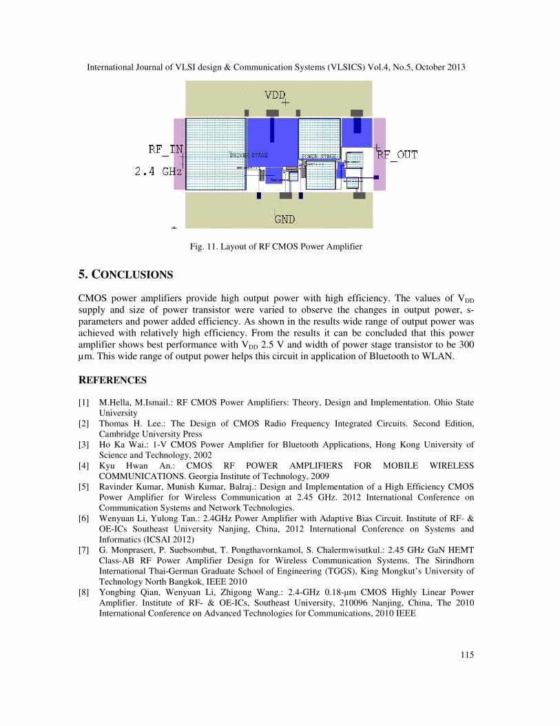
Fig. 11. Layout of RF CMOS Power Amplifier
5. CONCLUSIONS
CMOS power amplifiers provide high output power with high efficiency. The values of VDD
supply and size of power transistor were varied to observe the changes in output power, s-
parameters and power added efficiency. As shown in the results wide range of output power was
achieved with relatively high efficiency. From the results it can be concluded that this power
amplifier shows best performance with VDD 2.5 V and width of power stage transistor to be 300
µm. This wide range of output power helps this circuit in application of Bluetooth to WLAN.
REFERENCES
[1] M.Hella, M.Ismail.: RF CMOS Power Amplifiers: Theory, Design and Implementation. Ohio State
University
[2] Thomas H. Lee.: The Design of CMOS Radio Frequency Integrated Circuits. Second Edition,
Cambridge University Press
[3] Ho Ka Wai.: 1-V CMOS Power Amplifier for Bluetooth Applications, Hong Kong University of
Science and Technology, 2002
[4] Kyu Hwan An.: CMOS RF POWER AMPLIFIERS FOR MOBILE WIRELESS
COMMUNICATIONS. Georgia Institute of Technology, 2009
[5] Ravinder Kumar, Munish Kumar, Balraj.: Design and Implementation of a High Efficiency CMOS
Power Amplifier for Wireless Communication at 2.45 GHz. 2012 International Conference on
Communication Systems and Network Technologies.
[6] Wenyuan Li, Yulong Tan.: 2.4GHz Power Amplifier with Adaptive Bias Circuit. Institute of RF- &
OE-ICs Southeast University Nanjing, China, 2012 International Conference on Systems and
Informatics (ICSAI 2012)
[7] G. Monprasert, P. Suebsombut, T. Pongthavornkamol, S. Chalermwisutkul.: 2.45 GHz GaN HEMT
Class-AB RF Power Amplifier Design for Wireless Communication Systems. The Sirindhorn
International Thai-German Graduate School of Engineering (TGGS), King Mongkut’s University of
Technology North Bangkok, IEEE 2010
[8] Yongbing Qian, Wenyuan Li, Zhigong Wang.: 2.4-GHz 0.18-µm CMOS Highly Linear Power
Amplifier. Institute of RF- & OE-ICs, Southeast University, 210096 Nanjing, China, The 2010
International Conference on Advanced Technologies for Communications, 2010 IEEE
International Journal of VLSI design & Communication Systems (VLSICS) Vol.4, No.5, October 2013
116
[9] Cheng-Chi Yen Student Member, IEE and , Huey-Ru Chuang IEEE.: A 0.25um 20-dBm 2.4-GHz
CMOS Power Amplifier With an Integrated Diode Linearizer. MICROWAVE AND WIRELESS
COMPONENTS LETTERS, VOL. 13, NO. 2, FEBRUARY 2003
[10] Chia-Jun Chang, Po-Chih Wang, Chih-Yu Tsai, Chin-Lung Li, Chiao-Ling Chang, Han-Jung Shih,
Meng-Hsun Tsai, Wen-Shan Wang, Ka-Un Chan, and Ying-Hsi Lin.: A CMOS Transceiver with
internal PA and Digital Pre-distortion For WLAN 802.11a/b/g/n Applications., 2010 IEEE Radio
Frequency Integrated Circuits Symposium
[11] Yi Zhao, John R. Long, and Marco Spirito.: A 60GHz-band 20dBm Power Amplifier with 20% Peak
PAE. 2011 IEEE
[12] Ville Saari, Pasi Juurakko, Jussi Ryynanen and Kari Halonen.: lntegrated 2.4 GHz Class-E CMOS
Power Amplifier. 2005 lEEE Radio Frequency Integrated Circuits Symposium.