3d sensors
TRANSCRIPT

3Dc
3D sensorsSherwood Parker (U. of Hawaii)
Collaborators: High Energy Physics Projects
C. Kenney * (Molecular Biology Consortium)
C. Da Via, J. Hasi *, A. Kok, S. Watts (Brunel University)
S. Seidel, M. Hoeferkamp, I. Gorelov (University of New Mexico)
Members of the TOTEM, FP420, and Atlas Pixel groups.
G. Anelli, P. Jarron, M. Despeisse (CERN – Microelectronics group)
J. Morse (European Synchrotron Radiation Facility), E. Perozziello
* Collaborators: Structural Molecular Biology
E. Westbrook, A. Thompson (MBC), D. Gnani (LBL)

3Dc
8. TOTEM
9. active edges
10. yield
11. ATLAS pixels
12. FP420
13. molecular biology
14. conclusions
1. introduction
2. technology
3. calculations
4. first results
5. radiation damage
6. a puzzle (for now)
7. speed
Outline

3Dc
1. Solid-state semiconductor diode radiation sensorswere first made and used by Pieter Jacobus VanHeerden, a graduate student in the occupiedNetherlands during World War II, and have been in usefor over 50 years.
2. Planar technology was invented by Jean A. Hoerni ofFairchild Semiconductor in 1957- 8, around the time he,Robert Noyce and Gordon Moore left the original (andmassively mismanaged) semiconductor company,Shockley Semiconductor, to help form the second one,Fairchild Semiconductor. Within 6 years, planartechnology was used for silicon PIN diode sensors (T.Madden, W. Gibson, Rev. Sci. Instr. 34 (1963) 50).

3Dc
1945
(but work done during WW2 in Germanoccupied low-countries)

3Dc

3Dc

3Dc
Jean Hoerni, one ofShockley’s “8 traitors”, may
have invented the planarprocess during this time

3Dc

3Dc
(Herbert Anderson, a post-doc of Enrico Fermi, placed the last graphite blocks onthe first reactor, the night before the first controlled chain reaction was achieved.We were working together on the µ � e + γ experiment at the time he becameinterested in silicon detectors. Being rather slow, it took me 20 more years.)

3Dc

3Dc
1962

3Dc
The silicon sensor is thedark rectangle in thecenter. The width of thefanout if every strip wereread out: 1 meter

3DcPaul Karchin in front of a silicon telescope (the rest of the photograph: fanouts and cables).(Fermilab; 1985, 9 planes, 5 cm x 5 cm)

3Dc
1979

3Dc

3Dc

3Dc

3Dc
3. With planar technology, all fabricated elementsare located on or very close to the wafersurfaces, and oxide passivation layers tie upotherwise loosely bound surface charges,except along the saw-cut edges which must beseparated from the sensitive volume.
4. With the development of microstrips (England,Hyams, Hubbeling, Vermeulen, Weilhammer),and in 1982 - 4, the Microplex chip (Walker,Parker, Hyams) – the first custom VLSI readoutchip (which also used planar technology),silicon detectors started their wide use asparticle trackers in high-energy colliderexperiments.
5. Now, for experiments at the Large HadronCollider and for structural molecular biology, weare building a new kind of silicon sensor: 3D.

3Dc

3Dc
Some types of PIN radiation sensors
Why do we use the PIN structure? A semiconductor conducts, andat room temperature (except in 217 where I froze yesterday)
KT ≈ 0.026 eVand in semiconductors with ~ 1eV band gaps, thermal leakage
currents will dominate the signals.
● monolithic – very high signal-to-noise and so very high spatialresolution – but you have to make the readout circuit yourself.
● surface barrier – thin layers of metal with different work functionson top and bottom surfaces (thin entrance window butdelicate and temperamental)
● planar technology – diode junction (with its high fields) ends at anoxide layer – the current standard for high energy physics
field oxide
n or p implantp or n substrate

3Dc
●MAPS: epi layer (from commercial CMOS ) as the sensor:++ MUCH easier to order than make, no bump bonding, small
pixels possible, low input capacitance, thin (lowscattering, may help lower x-ray backgrounds)
– over most of the area charge carriers have to diffuse tocollection electrode so slow – and slow means extremeradiation hardness out of reach,thin means small signals or low x-ray detection efficiency
•planar / 3D active edge:
•standard (0.1 – 1 mm dead edge) drops to about ~1µm
•allows making large area detector from small units without deadbands crossing the image plane
•small units means high yield
• full 3D, active edge:
•fast
•extreme radiation hardness
•1µm dead edge

3Dc
3D silicon detectors were proposed in 1995by S. Parker, and active edges in 1997 by C.Kenney.
Combine traditional VLSI processing andMEMS (Micro Electro Mechanical Systems)technology.
Electrodes are processed inside the detectorbulk instead of being implanted on theWafer's surface.
The edge is an electrode! Dead volume at theEdge < 2 microns! Essential for-Large area coverage-Forward physics
INTRODUCTIONINTRODUCTION
1. NIMA 395 (1997) 3282. IEEE Trans Nucl Sci 46 (1999) 12243. IEEE Trans Nucl Sci 48 (2001) 1894. IEEE Trans Nucl Sci 48 (2001) 16295. IEEE Trans Nucl Sci 48 (2001) 24056. CERN Courier, Vol 43, Jan 2003, pp 23-267. NIMA 509 (2003)86-918. NIMA 524 (2004) 236-244

3Dc

3Dc
Some properties of 3D radiation sensors:
1 Long tracks can have short drift distances.
2 They have a lower ratio of peak to drift electricfields and so are less likely to have voltagebreakdowns.
3 They can be depleted, and have full sensitivity,at lower bias voltages.
4 The geometric nature of this means there willbe a low increase of depletion voltage withradiation damage.

3Dc
5. They have rapid charge collection, andcharges in perpendicular tracks come insimultaneously, rather than one at a time fromthe track ends, so they can make order-of-magnitude shorter pulses.
This speed is maintained, as expected, in heavilyirradiated sensors, and is useful in reducingcapture losses regardless of amplifier speeds.

3Dc
6. With fields directed away from, rather thanalong pixel or strip boundaries, they havereduced charge-sharing.
Charge-sharing may be used to improve spatialresolution, but may also take tracks belowthreshold in radiation damaged silicon,particularly with planar sensors.

3Dc
7. Active edges provide full sensitivity to withina few microns of the physical edges, in contrastwith the large dead regions of standard planartechnology (1.1 mm in the Atlas and CMS pixelsensors which must allow for many concentricguard rings).
8. Bias voltages can be made to vary across 3Dsensors. (useful if radiation damage and sodepletion voltages are much higher at, forexample, edges)

3Dc
BUT
they require more fabrication work.

3Dc
8. TOTEM
9. active edges
10. yield
11. ATLAS pixels
12. FP420
13. molecular biology
14. conclusions
1. introduction
2. technology
3. calculations
4. first results
5. radiation damage
6. a puzzle (for now)
7. speed
Outline

3Dc
Keys to the technology1. Plasma etchers can now make deep, near-vertical holes and trenches:
a. SF6 in plasma → F, F – → driven onto wafer by E fieldb. Si + 4F → SiF4 (gas)c. SF6 replaced with C4F8 → CF2 + other fragments whichd. form teflon-like wall coat protecting against off-axis F, F –e. repeat (a – d) every 10 – 15 seconds
2. At ~620ºC, ~0.46 Torr, SiH4 gas molecules bounce off the walls manytimes before they stick, mostly entering and leaving the hole. Whenthey stick, it can be anywhere, so they form a conformal polysiliconcoat as the H leaves and the silicon migrates to a lattice site.
3. Gasses such as B2O3, B2H6 (diborane), P2O5, and PH3 (phosphine)can also be deposited in a conformal layer, and make p+ and n+ dopedpolysilicon.
4. Heating drives the dopants into the single crystal silicon, forming p–njunctions and ohmic contacts there. Large E drift fields can endbefore the poly, removing that source of large leakage currents.
5. Active edges are made from trench electrodes, capped with an oxidecoat. Plasma dicing up to the oxide etch stop makes precise edges.

3Dc
12 µm
Dd
An early test structure byJulie Segal, etched andcoated (middle, right),showing conformal natureof poly coat.
An electrode hole, filled,broken (accidentally) in aplane through the axis,showing grain structure(below). The surface polyis later etched off.
290 µm
coated, top
coated, bottom
uncoated
Examples of etching and coating with polysilicon.

3Dc
8. TOTEM
9. active edges
10. yield
11. ATLAS pixels
12. FP420
13. molecular biology
14. conclusions
1. introduction
2. technology
3. calculations
4. first results
5. radiation damage
6. a puzzle (for now)
7. speed
Outline

3Dc
Potential 3D features from preliminary calculations:
~ 6% of E-breakdownfor V-bias = 10V
— 5V, higher curves: 10 to 50 V
50 µm
p
n
8 µm50 µm
Structure used incalculations.
Fabricated oneshave electrode
diameters ~50%larger; cell sizes~2× larger, andhave rows of
alternate n and pelectrodes.
2. Peak fields do not becomeexcessive with large radiation-
induced bulk damage.
1. Low depletion voltages andpeak fields.
~ 20% of E-breakdownfor V-bias = 50V
(and only 5V is neededto deplete)

3Dc
8. TOTEM
9. active edges
10. yield
11. ATLAS pixels
12. FP420
13. molecular biology
14. conclusions
1. introduction
2. technology
3. calculations
4. first results
5. radiation damage
6. a puzzle (for now)
7. speed
Outline
3Dc
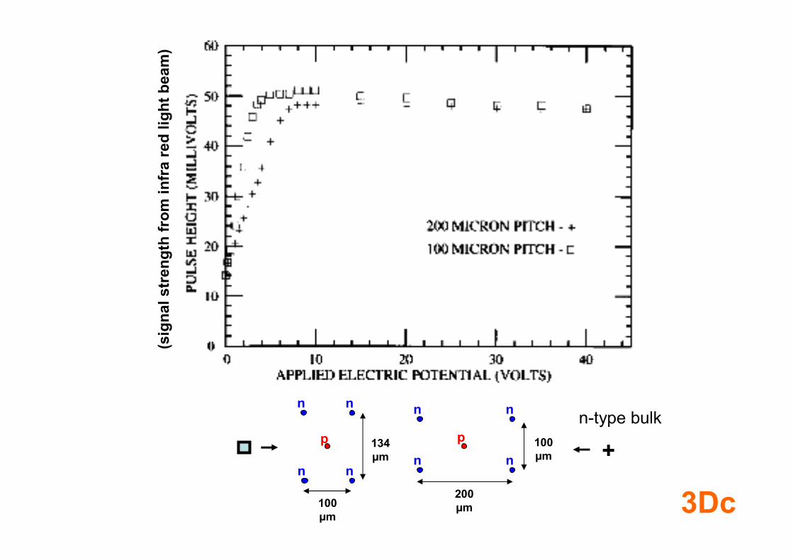
p
n
100µm
134µm
p
200µm
100µm
n
nn
n
n n
n
(sig
nal s
tren
gth
from
infr
a re
d lig
ht b
eam
)
+n-type bulk

3Dc
8. TOTEM
9. active edges
10. yield
11. ATLAS pixels
12. FP420
13. molecular biology
14. conclusions
1. introduction
2. technology
3. calculations
4. first results
5. radiation damage
6. a puzzle (for now)
7. speed
Outline

3Dc
3D performance after irradiation
90-Sr β signal in 3D sensor irradiatedby 10e15 SPS protons / sq cm, fullyreverse annealed, no implantedoxygen, room temperature.
IR µbeam signal vs. V-bias, 3Dsensor 10e15 55 MeV protons / sq.cm ≈ 1.8 10e15 1 MeV neutrons.Measured at room temp. Stored atlow temp. No beneficial or reverseannealing, no oxygen.Both sensors 181 µm thick, 100 µm × 134
µm cells, joined in rows for readout.

3Dc
0
5 0
10 0
15 0
20 0
0 1 2 3 4
F lu e n c e = 1 01 5 p ro to n s c m -2
Eff
ectiv
e D
rift
Len
gth
(mic
rons
)
E le c tric F ie ld ( V o lt/m icron )
E le c tro n s
H o le s
T = -2 0 oC
( Nucl. Instr. and Meth. A 509 (2003) 86 – 91)

3Dc
8. TOTEM
9. active edges
10. yield
11. ATLAS pixels
12. FP420
13. molecular biology
14. conclusions
1. introduction
2. technology
3. calculations
4. first results
5. radiation damage
6. a puzzle (for now)
7. speed
Outline

3Dc

3Dc
no low-side tail, sovery few, if any, events
with partial chargecollection efficiency

3Dc
linescan through p+ electrodecolumn and across active edge
linescan
0 20 40 600
50
100
AD
C c
ount
s
Energy (keV)
1.73keV
ID 3
rd h
arm
onic
15V bias
100 200 3000
3000
6000
Win
dow
cou
nt in
tegr
al to
24.
9keV
position (microns)
thresh6.5keVthresh10keVthresh15keV
electrode pitch 150µm
230 235 240 245 250 255 260 265 2700
3000
6000
15µm
p+ electrode
edge responseover ~10µm

3Dc
X5 (Totem) beam test – cell uniformity measurements
Center: data is further projected onto one quadrant. Null-field points are at upperright and lower left. n - - bulk and n+ active edges.
Observed 3D hits / predicted telescope hits as a function of position within the 100 µm x200 µm non-edge cells. To improve statistics, the hits for all cells are superimposed.
(Note: 3D discriminator thresholds can magnify the true collection efficiency differences.)
Left above: grid with pelectrodes on corners.
Right above: grid with pelectrodes in center.
p
n

3Dc
1. Differences in electrode diameters andthermal history (increased Dt increasesdopant diffusion distances and radiusof built-in fields, and can increase grainsizes – the N electrodes were donefirst).
2. The dopant gasses available at SNFproduce an oxide layer on the holesurface which remains after the hole isfilled; they may differ in radii andeffectiveness as barriers.
3. Electrons and holes have differentdiffusion rates and lifetimes in the polyelectrodes.
4. Note: The CERN -- X5 beam test datashows counts, not signal heights, anddiscrimination levels will affect theresults.
Some possible sources of the observed differences incollection efficiencies seen from n and p electrodes:
(from Kamins –Polycrystalline siliconfor integrated circuit
applications)
electron lifetimevs. grain size

3Dc
8. TOTEM
9. active edges
10. yield
11. ATLAS pixels
12. FP420
13. molecular biology
14. conclusions
1. introduction
2. technology
3. calculations
4. first results
5. radiation damage
6. a puzzle (for now)
7. speed
Outline

3Dc
1. 3D lateral cell size can be smaller than wafer thickness, so
2. in 3D, field lines end on cylinders rather than on circles, so
3. most of the signal is induced when the charge is close to theelectrode, where the electrode solid angle is large, so planarsignals are spread out in time as the charge arrives, and
4. Landau fluctuations along track arrive sequentially and maycause secondary peaks (see next slide)
5. if readout has inputs from both n+ and p+ electrodes,
6. for long, narrow pixels and fast electronics,
Speed: planar 3D
1. shorter collection distance
2. higher average fields for anygiven maximum field (price:larger electrode capacitance)
3. 3D signals are concentratedin time as the track arrives
4. Landau fluctuations arrivenearly simultaneously
5. drift time corrections can bemade
6. track locations within thepixel can be found
4.
4.
4.

3Dc
Potential 3D features from preliminary calculations:
3. Fast pulses. Current to the p electrode and the other 3n electrodes.
(The track is parallel to the electrodes through a cell center and anull point. V – bias = 10V. Cell centers are in center of anyquadrant. Null points are located between pairs of n electrodes.)
1 ns 3 ns
50 µm
p
n8 µm
50 µm

3Dc
rise times ≈ 3.5 ns fall times ≈ 3.5 ns
0.13 µm chips now fabricated – rise, fall times expected to be ≈ 1.5 ns
Resistive (transistor channel) feedback, and so a current amplifier.

3Dc
planar sensor pulse shape

3Dc
0.13 µm circuit – 8 pulsesin sequence

3Dc

3Dc

3Dc

3Dc

3Dc

3Dc

3Dc

3Dc
90Sr.20v.bias3.1
-1.00E-02
-8.00E-03
-6.00E-03
-4.00E-03
-2.00E-03
0.00E+00
2.00E-03
4.00E-03
1 23 45 67 89 111 133 155 177 199 221 243 265 287 309 331 353 375 397 419 441 463 485 507 529 551 573 595 617 639 661 683 705 727 749 771 793
time (62.5 ps / point)
v
Time Pts: channel 1 channel 2 channel 3
5ns
30ns

3Dc
90Sr.20v.bias3.2
-5.00E-03
-4.00E-03
-3.00E-03
-2.00E-03
-1.00E-03
0.00E+00
1.00E-03
2.00E-03
3.00E-03
1 23 45 67 89 111 133 155 177 199 221 243 265 287 309 331 353 375 397 419 441 463 485 507 529 551 573 595 617 639 661 683 705 727 749 771 793
time (62.5 ps / point)
v
Time Pts: channel 1 channel 2 channel 3
5ns
30ns

3Dc
90Sr.20v.bias3.3
-5.00E-03
-4.00E-03
-3.00E-03
-2.00E-03
-1.00E-03
0.00E+00
1.00E-03
2.00E-03
1 23 45 67 89 111 133 155 177 199 221 243 265 287 309 331 353 375 397 419 441 463 485 507 529 551 573 595 617 639 661 683 705 727 749 771 793
time (62.5 ps / point)
v
Time Pts: channel 1 channel 2 channel 3
5ns
30ns

3Dc
90Sr.20v.bias3.4
-4.00E-03
-3.00E-03
-2.00E-03
-1.00E-03
0.00E+00
1.00E-03
2.00E-03
1 23 45 67 89 111 133 155 177 199 221 243 265 287 309 331 353 375 397 419 441 463 485 507 529 551 573 595 617 639 661 683 705 727 749 771 793
time (62.5 ps / point)
v
Time Pts: channel 1 channel 2 channel 3
5ns
30ns

3Dc
90sr.20v.bias3.5
-4.00E-03
-3.00E-03
-2.00E-03
-1.00E-03
0.00E+00
1.00E-03
2.00E-03
1 23 45 67 89 111 133 155 177 199 221 243 265 287 309 331 353 375 397 419 441 463 485 507 529 551 573 595 617 639 661 683 705 727 749 771 793
time (62.5 ps / point)
v
Time Pts: channel 1 channel 2 channel 3
5ns
30ns

3Dc
90sr.20v.bias3.6
-1.20E-02
-1.00E-02
-8.00E-03
-6.00E-03
-4.00E-03
-2.00E-03
0.00E+00
2.00E-03
4.00E-03
6.00E-03
1 23 45 67 89 111 133 155 177 199 221 243 265 287 309 331 353 375 397 419 441 463 485 507 529 551 573 595 617 639 661 683 705 727 749 771 793
time (62.5 ps / point)
v
Time Pts: channel 1 channel 2 channel 3
5ns
30ns

3Dc
8. TOTEM
9. active edges
10. yield
11. ATLAS pixels
12. FP420
13. molecular biology
14. conclusions
1. introduction
2. technology
3. calculations
4. first results
5. radiation damage
6. a puzzle (for now)
7. speed
Outline

3Dc

3Dc
Totem – total cross section, elastic scattering,diffraction dissociation at the LHC – forward,
Roman pot silicon detectors
sensor to be sensitive asclose to this edge as
possible

3Dc
CERN-LHCC-2004-002TOTEM-TDR-001
7 January 2004Technical Design Report
The TOTEM experiment will measure the total pp cross section and study elasticscattering and diffractive dissociation at the LHC. More specifically, TOTEM willmeasure:* the total cross-section with an absolute error of 1mb by using the luminosityindependent method. This requires the simultaneous measurement of the elasticpp scattering down to the four-momentum transfer of -t ≈ 10-3 GeV2 and of theinelastic pp interaction rate with an adequate acceptance in the forward region;* elastic proton scattering over a wide range in momentum transfer up to -t ≈ 10GeV2;•diffractive dissociation, including single, double and central diffraction topologiesusing the forward inelastic detectors in combination with one of the large LHCdetectors.
From the minutes of the TOTEM Collaboration Board, Feb. 16, 2005:
* * * *The suggestion I to keep two technologies: 3D strips and planar with CTS.3Dstrips have a better edge behavior while the Russian CTS are lessexpensive. This choice does not require extra financing and manpowerresources from the experiment. SW says that in the present situation itwill be difficult for Brunel to contribute, but agrees that it is a good policyto have two vendor. Everybody agrees.

3Dc
8. TOTEM
9. active edges
10. yield
11. ATLAS pixels
12. FP420
13. molecular biology
14. conclusions
1. introduction
2. technology
3. calculations
4. first results
5. radiation damage
6. a puzzle (for now)
7. speed
Outline
3Dc
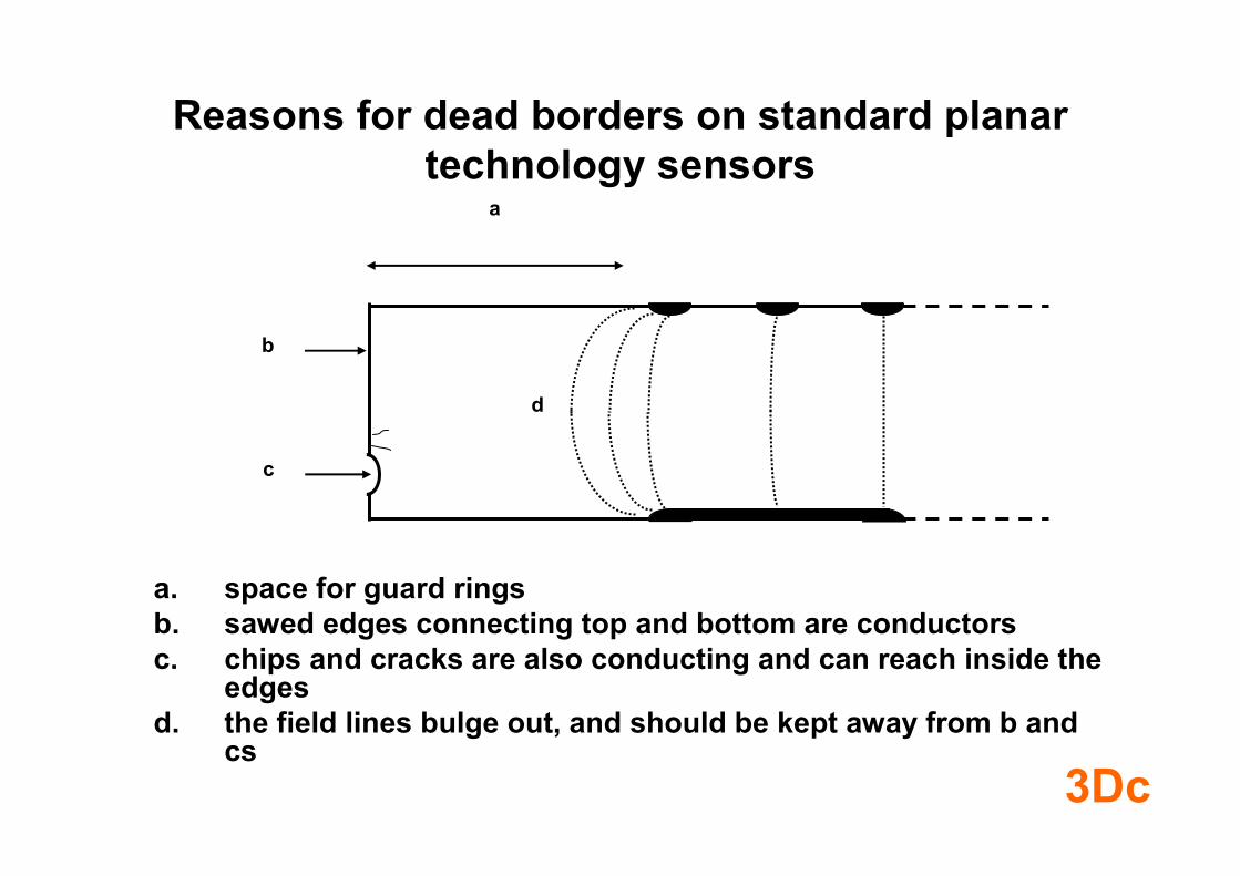
Reasons for dead borders on standard planartechnology sensors
a
b
c
d
a. space for guard ringsb. sawed edges connecting top and bottom are conductorsc. chips and cracks are also conducting and can reach inside the
edgesd. the field lines bulge out, and should be kept away from b and
cs

3Dc
ActiveEdges
support wafer oxide
sensor wafer
p n n
support wafer oxide
p n
p
n
poxide
1. etch border trenches
2. diffuse in dopant
3. grow protective oxidecover
4. fill trench with poly
5. vertical, directed etch(to dotted lines)
6. turn off sidewallprotection step
7. isotropic etch to oxidestop
8. additional steps are notincluded on this slide(and note, bondingoxide to support wafernot colored )
9. n and p electrodes can bereversed
3Dc
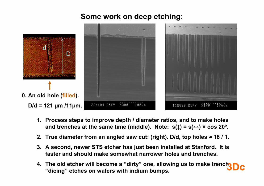
Some work on deep etching:
1. Process steps to improve depth / diameter ratios, and to make holesand trenches at the same time (middle). Note: s(↕) = s(↔) × cos 20º.
2. True diameter from an angled saw cut: (right). D/d, top holes ≈ 18 / 1.
3. A second, newer STS etcher has just been installed at Stanford. It isfaster and should make somewhat narrower holes and trenches.
4. The old etcher will become a “dirty” one, allowing us to make trench“dicing” etches on wafers with indium bumps.
Dd
0. An old hole (filled).
D/d = 121 µm /11µm.

3Dc
X-ray microbeam results for a 3D sensor
X-ray micro-beam scan, in 2 µm steps, of a 3D, n bulk and edges, 181µm thick sensor. The left curve is for the edge p channel. Thehorizontal scale is in µm; the vertical is arbitrary. The small dip in eachcenter is from nearby 3D electrodes. The left edge tail is fromreflected gold x-rays and from leakage current.
0
10
20
30
40
0 100 200 300 400
edgeinter-strip
boundaries

3Dc
0
60
120
180
240
300
360
0918273645
54
microns
45-54
36-45
27-36
18-27
9-18
0-9
Current from scan in an x-ray microbeam, of another 3D sensor witha photomicrograph of the corresponding part on the right. Grid lines
are spaced 10µm apart.

3Dc
Totem X5 test beam at CERN.
1. The 3D planes: 16 -- 200 µm (y) by 40 -- 100 µm (x) cells, n bulk and edges.
2. They are tied together in x-rows for a y readout using SCTA integratedcircuits and a scintillator trigger.
3. The 3D planes are centered between a 4-plane silicon strip telescope with 4y planes and 2 x ones. σy = ± 4 µm.
4. The beam was set for 100 GeV muons.

3Dc
Some results from the CERN X5 beam test(100 GeV muons)
Measured hit position in 3Dsensor plane #3 vs. predictedposition from beam telescope.
Fitted 3D sensor width = 3,203 ±4 µm.Drawn width = 3,195 µm. Sensorefficiency = 98%. System efficiency lessdue to DAQ, triggering electronics.

3Dc
GUARD RINGSinks surface leakage current
E-fieldp + Al
n + Al
i
E-field p + + Al
n ++ + Au
n++
PLANAR PLANAR / 3D =PLANAR DETECTOR + DOPANT DIFFUSED IN FROM DEEPETCHED EDGE, CAPPED WITH OXIDE, FILLED WITHPOLYSILICON, POLY FINALLY ETCHED AWAY
Microcracks, chips etc..
PLANAR DEVICES WITH 3D ACTIVE EDGESPLANAR DEVICES WITH 3D ACTIVE EDGES
MEDICI Simulation of theequipotential lines for a70 V bias 300 µm device(J. Segal MBC)
Depletion boundaryDepletion boundary
3Dc
8. TOTEM
9. active edges
10. yield
11. ATLAS pixels
12. FP420
13. molecular biology
14. conclusions
1. introduction
2. technology
3. calculations
4. first results
5. radiation damage
6. a puzzle (for now)
7. speed
Outline

3DcFigure 6. Stanford clean room near diffusion
furnaces, looking in the direction of the red arrow.

3Dc
Pictures of clean rooms like the one precedingare familiar, but many other things are neededfor high yield, for example: specific, carefulchecking of the results of each of the 37 mainsteps and of the many sub-steps, cleanliness notjust of the room and air, but of everything used –tools, chemicals, cassettes, etc.
The deep etching may leave an uneven surfacethat makes it difficult to spin on a uniform layerof photoresist for a following lithography step. Ifthis step is a deep etch, a thick resist is needed.They seem to have a higher level of particulatesand clumps of resist.
Active edge fabrication requires support wafers,which must be oxide-bonded to the sensor waferunder extremely clean conditions.

3Dc
The following specific steps were added to the fabricationprocedure for the two-order-of-magnitude larger, 9 cm2 planar /3D active edge Totem sensors:1. The wafers were carefully inspected after every litho step. Ifdefects were seen, the resist was removed, new resist wasapplied, and the wafers were re-spun and re-exposed.2. Defects in the thick resist used for the trench etch werecovered with polyimide.3. The surface planarity in the region of the dips at the centers ofthe poly-filled electrodes was improved by etching the poly offthe top surface, and then repeating the fill and etch procedure.4. The plasma dice lane was widened from 50 microns to 120microns. The more open trench prevented the formation ofsilicon chips along the trench edges. This seems to haveeliminated this defect class, which caused a 25% loss for the firstbatch.5. Evaporated aluminum instead of sputtered gold was used forthe backside contact.
3Dc
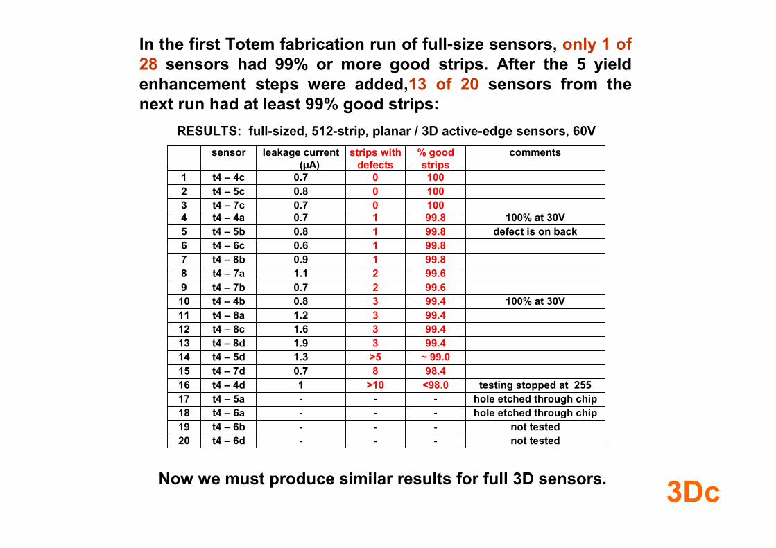
not tested---t4 – 6d20not tested---t4 – 6b19
hole etched through chip---t4 – 6a18hole etched through chip---t4 – 5a17testing stopped at 255<98.0>101t4 – 4d16
98.480.7t4 – 7d15~ 99.0>51.3t4 – 5d1499.431.9t4 – 8d1399.431.6t4 – 8c1299.431.2t4 – 8a11
100% at 30V99.430.8t4 – 4b1099.620.7t4 – 7b999.621.1t4 – 7a899.810.9t4 – 8b799.810.6t4 – 6c6
defect is on back99.810.8t4 – 5b5100% at 30V99.810.7t4 – 4a4
10000.7t4 – 7c310000.8t4 – 5c210000.7t4 – 4c1
comments% goodstrips
strips withdefects
leakage current(µA)
sensor
RESULTS: full-sized, 512-strip, planar / 3D active-edge sensors, 60V
In the first Totem fabrication run of full-size sensors, only 1 of28 sensors had 99% or more good strips. After the 5 yieldenhancement steps were added,13 of 20 sensors from thenext run had at least 99% good strips:
Now we must produce similar results for full 3D sensors.

3Dc
8. TOTEM
9. active edges
10. yield
11. ATLAS pixels
12. FP420
13. molecular biology
14. conclusions
1. introduction
2. technology
3. calculations
4. first results
5. radiation damage
6. a puzzle (for now)
7. speed
Outline

3Dc
More typical spectrum TOT spectrum for the best looking pixel
Possible steps for improvement of fabrication yields:• Improvement of fabrication steps (as was done for planar / 3D active edge sensors).• Use solder bumps at wafer scale.• 2-3 month fabrication run rather than 5 week run.• Use of P- type bulk so diode junctions always at signal electrodes so one badjunction does not short bias supply.• Probably won’t need to reduce signal electrode capacitance using poly-resistorisolation of bias electrodes, but it remains a possibility.

3Dc
Fabrication
1. It would be best to have commercial fabricators. Somediscussions have been held with companies makingsensors.
2. However the companies currently having thespecialized plasma etchers used for 3D fabrication tendto be micromachining companies, not sensor ones.
3. Second sources, as some LHC collaborations canconfirm, can be important.
4. It is difficult to get even a first source, in the absence ofthe prospect of an order.
5. We can make the needed sensors at Stanford, ifnecessary. At the minimum, that will supply a secondsource. We now discuss fabrication at Stanford:

3Dc
ModuleProduction
10 Modules per Wafer
150 mm Wafers
230 Wafers Divided byYield
or (next slide) make readout-chip size units:

3Dc
ChipProduction
•209 Chips per Wafer
•(i.e. one active edgesensor chip for eachreadout chip)
•150 mm Wafers
•170 Wafers Divided by Yield
•Chip Yield is Probably Much Higher then ModuleYield

3Dc
Module LayoutDimensions:61mm by 16.4 mm
10 Modules Per 150 mmWafer
Area Used:10,000 mm2 – 10Modules
80 Percent of Chip Area

3Dc
Chip LayoutDimensions:7.6 mm by 8.2 mm
209 Chips Per 150 mmWafer
Area Used:13,025 mm2

3Dc
Budget
Divide by Device Yield ( Range 40 to 75 Percent)
Add overhead and Contingency
So at least Double these Amounts
Item Modules NO/DRIE Modules w/DRIE Chips w/DRIEFab Usage $200,000 $100,000 $80,000Thinning $20,000 $20,000 $20,000Float Zone Wafers $23,000 $23,000 $17,710Test & Fusion Wafers $10,000 $10,000 $7,700Supplies $20,000 $20,000 $20,000DRIE Etcher $0 $350,000 $350,000Masks $30,000 $30,000 $30,000Personnel $800,000 $400,000 $320,000
TOTAL $1,103,000 $953,000 $845,410
Time (Months) 24 12 9.2

3Dc
8. TOTEM
9. active edges
10. yield
11. ATLAS pixels
12. FP420
13. molecular biology
14. conclusions
1. introduction
2. technology
3. calculations
4. first results
5. radiation damage
6. a puzzle (for now)
7. speed
Outline

3Dc
CERN-LHCC-2005-025LHCC-I-015
FP420 (L.O.I.)An R&D Proposal to Investigate the Feasibility of Installing Proton Tagging
Detectors in the 420m Region at LHCM. G. Albrow1, T. Anthonis2, M. Arneodo3, R. Barlow2,4, W. Beaumont5, A. Brandt6, P. Bussey7, C. Buttar7,M. Capua8, J. E. Cole9, B. E. Cox2,*, C. DaVià10, A. DeRoeck11,*, E. A. De Wolf5, J. R. Forshaw2, J.Freeman1, P. Grafstrom11,+, J. Gronberg12, M. Grothe13 , J. Hasi10, G. P. Heath9, V. Hedberg14,+, B. W.Kennedy15, C. Kenney16, V. A. Khoze17, H. Kowalski18, J. Lamsa19, D. Lange12, V. Lemaitre20, F. K.Loebinger2, A. Mastroberardino8, O. Militaru20, D. M. Newbold9,15, R. Orava19, V. O’Shea7, K. Osterberg19,S. Parker21, P. Petroff22, J. Pinfold23, K. Piotrzkowski20, M. Rijssenbeek24, J. Rohlf25, L. Rurua5, M. Ruspa3,M. G. Ryskin17, D. H. Saxon7, P. Schlein26, G. Snow27, A. Sobol27, A. Solano13, W. J. Stirling17, M.Tasevsky28, E. Tassi8, P. Van Mechelen5, S. J. Watts10, T. Wengler2, S. White29, D. Wright12
1. Executive Summary
The physics potential of forward proton tagging in the 420m region at the LHChas only been fully appreciated within the last few years. By detectingprotons that have lost less than 1% of their longitudinal momentum, a richQCD, electroweak, Higgs and BSM program becomes accessible, with thepotential to make measurements which are unique at LHC, and difficult evenat a future linear collider.
(p. 2)

3Dc
8. TOTEM
9. active edges
10. yield
11. ATLAS pixels
12. FP420
13. molecular biology
14. conclusions
1. introduction
2. technology
3. calculations
4. first results
5. radiation damage
6. a puzzle (for now)
7. speed
Outline

3Dc
Structural Molecular Biology
1. The human genome project has given us a first draft for the order ofthe base pairs in our DNA, specifying the order in which amino acids(one for each three base pairs) are assembled to make proteins.
2. It does NOT tell us what the proteins look like or what they do.
3. Understanding that—the keys to their biological activity – requiresknowledge of their three dimensional shape and charge distribution.
4. Even though they are made in a linear fashion as the RNA is read out,they fold – or are folded – into highly complex shapes. Thesequence may also be altered.
5. They are far too small to be seen in an optical microscope, have toomuch internal detail for scanning tunneling microscopes, and are toodelicate for the vacuum and electrical conditions of an electronmicroscope.

3Dc
6. Their structure can be determined by illuminating them withcollimated, mono-energetic x-rays, and measuring thescattering intensity over a range of angles. Each outgoingangle gives information from a different view of the molecule.
7. Extra intensity measurements with sulfur replaced byselenium, or of anomalous scattering near an absorptionedge, are used to give phase information.
8. To get enough counts, many molecules must be used. Tokeep the patterns coherent, they must be aligned in acrystalline form.
9. We plan to use an array of shingled, active-edge, 3D siliconsensors to measure those patterns.

3Dc
Now use phosphor screen / multi-fibreoptic bundle /CCD mosaic readout.Up to 300 x 300mm2 square and with PSF ~100µm FWHM
Limitations:•intense diffraction spots in image spoil the usable dynamic range(which for a CCD is always < “16 bits”)
•Protein Samples rapidly degrade in the X-ray beam(synchrotron IDs -->1013 photons/sec).CCD systems require a few seconds to readout, while strongly diffractingcrystals can saturate the CCD full well capacity in ~0.1sec
• Long tails associated with the ‘Lorentzian’ spatial response of thephosphor screen+optics. This limits the precision of flat fieldcorrections and measurement of close-spaced diffraction peaks…
Crystallography area detectors

3Dcc: side view of one column
(all sensors normal to diffracted x-rays)
copper
mounts
and heat
sinks
support bar readout chips(under sensors)
adjacentsensorsoverlapwithout
touching
1 cm
sensors
b: front (x-ray) view of 1 column
gatearrays
a: top view of 3 modules (in central plane)
support bar(behind plane of sensors)
crystal sample
copper mountand heat sink
to computer
gate arrayreadout chip
silicon sensor
to crystal sample(X ray diffraction source)
alignment blockssupport bar
flexible printed circuit
3DX x-ray detector array for structural molecular biology

3Dc
Pixel Design1. 64 x 64 pixels, each 150 µm x 150 µm.2. Readout pixels are only 144 µm x 150 µm,
keeping the readout chip fully under the sensor.3. Each pixel has an integrating amplifier.4. 2 rows are read out together, using 128 lines.5. Integration resumes after 1 µs.6. Pulse heights are digitized in a Wilkinson ADC.7. Readout moves to next two rows after an
additional µs.8. Data is output to the computer from alternate
buffers. The full sensor is readout every 64 µs.9. Charge-shared signals can be recombined in
the computer.10. Small replaceable units for efficiency (PILATUS
dead area = 8.1% (pixels) + 4.4% (gaps) = 1 / 8)

3Dc
Wilkinson ADCcommon ramp
Cr
off-chipclock
8-bit count bus
(reset on until flip)
S-off(pixeloff)S3
S2
S1
C1’
C1
SignalIn
Calibration In
5-bit DACC-cal
S4
S-gain
TO BUS
C2
C-memV-ped
Pixel Cell
64 x 64pixelarray
alternate rowsto next line
receiver,
(digital linescrossing
output busare
differential)
8-bit dual edge Graycode counter
•128 line receivers (2 rows)•128 ADCs (1.5 µs conv. time)•128 x 8 bits conversion RAMs
•128 x 8 bits output shift registers
8-bit DAC (V-ref)
S6
S5
column bus line receiver(has large input C)
8-bit DAC: I-internal
4-bits: set rampslope and sign
ADC comparatordelayed
latchlatch
C-latch
C-ped
V-ref. baselinecomparator -
common modebaseline correction
8-bit RAM a
channel 0 (of 128)
8-bit RAMb
8-bit output bus
row read address
C3
Figure 6. Block diagram of VLSI readout circuit.
Capacitor values (fF): C1=37, C1’=25, C2=75, C3=25, C-mem=900C-receiver =450, C-cal=16, C-latch ≈10, C-ped ≈ 1,000, C-column bus ≈ 3,000
Vr1 Vr2
Vr2
Vr1
S1 to S6 ADC Graycodereset
Reset all comparatorsSelect ramp initial offset
PHASE GENERATOR
Output control – RAM a or b to bus,7-bit column address select,load 8-bit data to output bus signal.

3Dc
Figure 13. Sensor – readout chip – chip carrier mounted on a circuit board and placed on a probe station (left), and at largermagnification (center and right). The wire bonds to the chip carrier are visible in the right view.

3DcFigure 16. Map of 8 x 8 pixel area surrounding aiming point of the x-ray beam.
1 2 3 4 5 6 7 8S1
S4S7
0.00
0.10
0.20
0.30
0.40
0.50
0.60
0.70
0.80
0.90
1.00
Frac
tion
of p
eak
pixe
l
Horizontal pixels
Vertical pixels

3Dc
0
200
400
600
800
1000
1200
0 10 20 30 40 50 60 70 80 90 100 110 120 130 140 150 160 170 180ADC channel
even
t cou
nt Raw Data

3Dc
0.00
5000.00
10000.00
15000.00
-1 0 1 2 3 4 5 6 712keV photons
equi
vale
nt e
vent
cou
nt
Peak EnvelopeCalibrated DataPossonian-Gaussian Fit

3Dc
8. TOTEM
9. active edges
10. yield
11. ATLAS pixels
12. FP420
13. molecular biology
14. conclusions
1. introduction
2. technology
3. calculations
4. first results
5. radiation damage
6. a puzzle (for now)
7. speed
Outline

3Dc
Conclusions1. Expectations for 3D sensors from the initial calculations have
been verified:
a. They are fast. Amplifier-limited rise and fall times of 3.5 ns atroom temperature, even after irradiation by 10e15 / sq. cm. havebeen measured. (A new 0.13 micron line-width amplifier, has arise time of 1.5 ns, makes pulses of 4.5 to 5 ns full width at thebase.)
b. They deplete at low voltages (~ 5 – 10 V) and have wideplateaus for infrared microbeam signals.
c. Good resistance to radiation damage has been verified. (Asensor not designed for radiation hardness, with no oxygendiffusion, and no beneficial annealing had a signal plateau from105 V to 150 V for an infrared light beam after irradiation by10e15 55 MeV protons sq. cm (≈ 1.8 e 15 1-MeV neutrons / sq.cm.).

3Dc
2. Outside the center parts of the electrodes, chargecollection is efficient: a 14 KeV x-ray line from a 241-Am source fits a symmetric Gaussian with a sigma of282 eV.
3. Sensors have reasonable leakage currents: about 1 nA/ cu. mm. Active edge channels have the same leakagecurrents as interior ones. (Some recent runs have hadhigher leakage currents, possibly due to an iron-contaminated furnace tube.)
4. 4. A new feature, active edges, has been developed,bringing full sensitivity to within several microns of thephysical edges.

3Dc
5. A new kind of sensor has been fabricated and tested :planar / 3D – active edges. It has planar electrodes onthe top surface, a single opposite-type implant on thebottom, and a 3D electrode on its edges which iscontinuous with the bottom. It has edge propertiessimilar to those of full 3D sensors, with no dead volumeanywhere inside, but without the speed or radiationhardness of full 3D.
6. Production of planar / 3D – active edges sensors forTOTEM should start this year.
7. NIH sensors are made using the same technology asTOTEM and will share the same wafer.
8. An R&D fabrication run of full 3D sensors for theATLAS pixel B layer replacement, for the ATLAS pixelupgrade, and for FP420 is now underway.