decision diagrams based on-line testing of digital vlsi
TRANSCRIPT

Decision Diagrams Based On-line Testing of
Digital VLSI Circuits
Pradeep Kumar Biswal


Decision Diagrams Based On-line Testing of
Digital VLSI Circuits
Thesis submitted in partial fulfillment of the requirements
for the degree of
Doctor of Philosophy
by
Pradeep Kumar Biswal
Under the supervision of
Dr Santosh Biswas
Department of Computer Science and Engineering
Indian Institute of Technology GuwahatiGuwahati 781039, India
July 12, 2017


“Bande Purushottamam”
Dedicated at the holy feet of my Beloved Guru Sri Sri Thakur
Anukulchandra and guiding star of my life Pujaniya Babaida.


Declaration
I, Pradeep Kumar Biswal, confirm that:
a. The work contained in this thesis is original and has been done by myself
and the general supervision of my supervisor.
b. The work has not been submitted to any other Institute for any degree or
diploma.
c. Whenever I have used materials (data, theoretical analysis, results) from
other sources, I have given due credit to them by citing them in the text of
the thesis and giving their details in the references.
d. Whenever I have quoted written materials from other sources, I have put
them under quotation marks and given due credit to the sources by citing
them and giving required details in the references.
Place: IIT Guwahati Pradeep Kumar Biswal
Date: Research Scholar
Department of Computer Science and Engineering,
Indian Institute of Technology Guwahati,
Assam-781039, India


Certificate
This is to certify that this thesis entitled “Decision Diagrams Based On-line Testing of
Digital VLSI Circuits” submitted by Pradeep Kumar Biswal, to the Indian Institute
of Technology Guwahati, for partial fulfillment of the award of the degree of Doctor of
Philosophy, is a record of bona fide research work carried out by him under my supervision
and guidance.
The thesis, in my opinion, is worthy of consideration for award of the degree of Doctor of
Philosophy in accordance with the regulations of the institute. To the best of my knowledge,
the results embodied in the thesis have not been submitted to any other university or institute
for the award of any other degree or diploma.
Place : I.I.T. Guwahati, India (Santosh Biswas)
Date: Associate Professor,
Dept. of Computer Science and Engineering,
Indian Institute of Technology, Guwahati


Acknowledgements
I wish to express my most sincere gratitude and appreciation to my supervisor,
Dr. Santosh Biswas, for his support, help and guidance throughout the research.
His continued support led me the right way to bring forth this thesis successfully.
I would like to extend my appreciation to my doctoral committee members,
Prof. Jatindra Kumar Deka, Prof. Hemangee K. Kapoor and Prof. Roy Paily
Palathinkal for providing constructive suggestions related to my work. I wish to
thank Prof. Diganta Goswami, Head of the Department of Computer Science
and Engineering and other faculty members for their support and help. I would
also like to acknowledge the efforts devoted by all the teachers starting from my
school days.
I am grateful to a number of people of IIT Guwahati who, over the last few years,
have helped me by providing valuable ideas and suggestions. They include Prof.
Sukumar Nandi, Prof. Gautam Biswas (Director), Prof. Gautam Barua (former
Director), Dr. Aryabartta Sahu and Dr. Arnab Sarkar. I would also like to take
this opportunity to thank all my friends, only to name a few, Malaya, Badri,
Vaibhav, Vivek, Sandip, Lalatendu, Shirshendu, Biswajit, Shounak, Basant,
Mayank, Nandi, Debasish, Pratap, Shibananda, Ananda, Mrityunjay, Pradeep,
Amrita, Rabindra, who directly and indirectly helped in finishing my thesis. I
am thankful to all my near and dear Guru-bhais (disciples of Sri Sri Thakur
Anukulchandra) for their moral support and love which helped me to overcome
all the tough situations in my life.
Last but most important are my parents and other family members whose
blessings and love made my path of success. I am grateful to my father, mother,
uncle, aunt, brothers and sisters who have always supported me at every course
of my life and offered me constant encouragement and inspiration.


Abstract
The rapid increase in complexity of VLSI circuits with the advent of Deep Sub-Micron
(DSM) technology causes development of faults during their normal operation. In other
words, the probability of occurrence of faults in modern VLSI circuits after deployment is
high, even though they were tested successfully after manufacturing. Such faults cannot be
detected by off-line test or Built-In-Self-Test (BIST) techniques, thus, On-line Testing (OLT)
is becoming an essential part in Design for Testability (DFT). Most of the existing works
presented in the literature on OLT of digital circuits have emphasized on the followings:-
non-intrusiveness, totally self-checking, low area overhead, high fault coverage, low detection
latency, etc. However, in DSM era, several other factors need to be considered, namely
flexibility, coverage for advanced fault models, scalability, handling asynchronous circuits,
etc. Considering all these facts, the main objective of this thesis is to design and develop
efficient OLT schemes for detection of faults on-the-fly in digital VLSI circuits. All the
proposed algorithms for on-line tester design use Decision Diagrams (DDs) to improve the
scalability of the schemes.
All the existing works on OLT have ignored the issue of minimization of tap points
(i.e., measurement limitation) of the Circuit Under Test (CUT) by the on-line tester.
Minimization of tap points reduces load on the CUT and this in turn lowers the area
overhead of the tester, however, it compromises fault coverage and detection latency. As the
first contribution of the thesis, we propose an Ordered Binary Decision Diagram (OBDD)
based OLT scheme for digital circuits by considering “number of tap points” as a new design
parameter to provide flexibility in the OLT perspective. Experimentally, it is seen that
measurement limitation has minimal impact on fault coverage and detection latency but it
reduces area overhead of the on-line tester significantly.
The OLT schemes reported in the literature are mainly targeted towards the traditional
stuck-at fault model and only few of them are designed for bridging faults. However, most
of these techniques have considered only non-feedback bridging faults, because feedback
bridging faults may cause oscillations and detecting them on-line using logic testing is
vii

ABSTRACT
difficult. It may be noted that, not all feedback bridging faults cause oscillations and even if
some does, there are test patterns for which the fault effect can be manifested logically. In this
contribution, we propose an OBDD based OLT scheme for both feedback and non-feedback
bridging faults. Experimentally, we have seen that consideration of feedback bridging faults
along with non-feedback ones, improves fault coverage with marginal increase in the area
overhead compared to schemes only involving non-feedback faults.
The majority of works on OLT reported in the literature are at the gate level and
these schemes take reasonable computational time and have limited scalability. The reason
being these schemes work at bit level, leading to the state explosion problem. This issue
can be addressed by developing OLT schemes at higher description levels of the circuits.
In the third contribution, we propose a High Level Decision Diagram (HLDD) based OLT
scheme at Register Transfer Level (RTL) model of circuits in order to improve the scalability.
Experiments on different benchmark circuits show that the test generation time is greatly
improved, thus, large circuits can be easily handled. Further, it achieves lower area overhead
at similar fault coverage compared to OLT schemes at gate level.
Most of the OLT schemes are designed for synchronous circuits compared to asyn-
chronous circuits. There are very few works that have been proposed for OLT of asyn-
chronous circuits and most of them are based on the Mutex approach. The area overhead
of these schemes are quit high because of Mutex blocks, which are the main components of
the on-line tester. In the final contribution, we propose an OBDD based OLT scheme for
Speed Independent asynchronous (SI) circuits, which has low area overhead. The scheme
is applied to different SI benchmark circuits and it is found that the area overhead of the
on-line tester is much less compared to that of the existing Mutex approach.
Keywords: On-line Testing (OLT), fault models, synchronous circuit, asynchronous
circuit, circuit at Register Transfer Level (RTL), Binary Decision Diagram (BDD), High
Level Decision Diagram (HLDD), fault coverage, fault detection latency, area overhead.
viii

Contents
List of Figures xiii
List of Tables xvii
Nomenclature xix
1 Introduction 1
1.1 Introduction to OLT of digital VLSI circuits . . . . . . . . . . . . . . . . . . 4
1.2 Introduction to decision diagrams and their applications in digital circuit testing 6
1.3 Motivations and Contributions of the thesis . . . . . . . . . . . . . . . . . . 8
1.4 Organization of the thesis . . . . . . . . . . . . . . . . . . . . . . . . . . . . 12
2 Literature review: On-line Testing of Digital VLSI Circuits and Decision
Diagrams 13
2.1 Digital VLSI testing . . . . . . . . . . . . . . . . . . . . . . . . . . . . . . . 13
2.1.1 Structural vs. functional testing . . . . . . . . . . . . . . . . . . . . . 16
2.1.2 Fault models . . . . . . . . . . . . . . . . . . . . . . . . . . . . . . . 19
2.1.3 Test programming . . . . . . . . . . . . . . . . . . . . . . . . . . . . 21
2.1.4 Comparison of ATE based testing, BIST and OLT . . . . . . . . . . . 22
2.2 Literature review: On-line testing of digital VLSI circuits . . . . . . . . . . . 24
2.2.1 Signature monitoring in FSMs . . . . . . . . . . . . . . . . . . . . . . 25
2.2.2 Self-checking design using error detecting codes . . . . . . . . . . . . 28
2.2.3 Duplication schemes for OLT . . . . . . . . . . . . . . . . . . . . . . 32
2.2.4 On-line BIST . . . . . . . . . . . . . . . . . . . . . . . . . . . . . . . 34
2.2.5 Pros and cons of different OLT techniques . . . . . . . . . . . . . . . 35
2.3 Desired features of OLT schemes . . . . . . . . . . . . . . . . . . . . . . . . 35
2.3.1 Measurement limitation based flexibility in OLT . . . . . . . . . . . . 35
2.3.2 OLT schemes for advanced fault model . . . . . . . . . . . . . . . . . 37
ix

CONTENTS
2.3.3 OLT schemes for circuits at higher description level . . . . . . . . . . 39
2.3.4 OLT schemes for asynchronous circuits . . . . . . . . . . . . . . . . . 42
2.4 Complexity of generation of exhaustive set of test patterns for OLT . . . . . 43
2.4.1 Decision Diagrams . . . . . . . . . . . . . . . . . . . . . . . . . . . . 44
2.4.2 Testing of digital circuits using Decision Diagrams . . . . . . . . . . . 51
2.5 Conclusion . . . . . . . . . . . . . . . . . . . . . . . . . . . . . . . . . . . . . 53
3 On-line Testing with Measurement Limitation 55
3.1 Introduction . . . . . . . . . . . . . . . . . . . . . . . . . . . . . . . . . . . . 55
3.2 FSA framework under measurement limitation: Circuit modeling and FN -
detector design . . . . . . . . . . . . . . . . . . . . . . . . . . . . . . . . . . 57
3.2.1 Circuit modeling under single stuck-at fault . . . . . . . . . . . . . . 58
3.2.2 FN -detector design for FSA model of a circuit . . . . . . . . . . . . . 59
3.3 Efficient construction of FN -detector . . . . . . . . . . . . . . . . . . . . . . 65
3.3.1 OBDD based procedure for exhaustive test pattern generation for the
NSF block under full measurement . . . . . . . . . . . . . . . . . . . 68
3.3.2 OBDD based procedure for determination of FD-transitions under
measurement limitation . . . . . . . . . . . . . . . . . . . . . . . . . 71
3.3.3 FN -detector design for Output Function block of the circuit . . . . . 73
3.4 Experimental evaluation . . . . . . . . . . . . . . . . . . . . . . . . . . . . . 76
3.4.1 Trade-offs in FN -detector design: detection latency, fault coverage,
measurement limitation and area overhead . . . . . . . . . . . . . . . 77
3.5 Conclusion . . . . . . . . . . . . . . . . . . . . . . . . . . . . . . . . . . . . . 82
4 On-line Testing for Feedback Bridging Faults 83
4.1 Introduction . . . . . . . . . . . . . . . . . . . . . . . . . . . . . . . . . . . . 83
4.2 Circuit modeling and FN-detector design using FSA framework . . . . . . . 84
4.2.1 Circuit modeling under bridging faults . . . . . . . . . . . . . . . . . 85
4.2.2 FN -detector construction from the FSA model of the CUT . . . . . . 91
4.3 Efficient construction of FN -detector for bridging faults . . . . . . . . . . . 92
4.3.1 Partition of the CUT into sub-circuits using cones of influence . . . . 93
4.3.2 OBDD based procedure for generation of exhaustive set of FD-
transitions for non-feedback bridging faults . . . . . . . . . . . . . . 96
4.3.3 OBDD based procedure for generation of exhaustive set of FD-
transitions for feedback bridging faults . . . . . . . . . . . . . . . . . 98
x

CONTENTS
4.3.4 OBDD based procedure for illustration of an oscillating feedback
bridging fault . . . . . . . . . . . . . . . . . . . . . . . . . . . . . . . 105
4.4 Experimental evaluation . . . . . . . . . . . . . . . . . . . . . . . . . . . . . 106
4.4.1 Fault coverage analysis . . . . . . . . . . . . . . . . . . . . . . . . . . 107
4.4.2 Area overhead analysis . . . . . . . . . . . . . . . . . . . . . . . . . . 108
4.5 Conclusion . . . . . . . . . . . . . . . . . . . . . . . . . . . . . . . . . . . . . 112
5 On-line Testing at Register Transfer Level 113
5.1 Introduction . . . . . . . . . . . . . . . . . . . . . . . . . . . . . . . . . . . . 113
5.2 High-Level Decision Diagram . . . . . . . . . . . . . . . . . . . . . . . . . . 114
5.3 Circuit modeling at RTL: Normal and faulty conditions . . . . . . . . . . . . 116
5.3.1 Circuit modeling using HLDD . . . . . . . . . . . . . . . . . . . . . . 120
5.3.2 RTL fault model and circuit modeling under fault. . . . . . . . . . . . 123
5.4 Generation of exhaustive set of FD-control-patterns and design of FN -detector127
5.4.1 Design of FN -detector . . . . . . . . . . . . . . . . . . . . . . . . . . 129
5.4.2 FN -detector design for combinational part of the RTL circuit . . . . 132
5.5 Experimental evaluation . . . . . . . . . . . . . . . . . . . . . . . . . . . . . 134
5.5.1 Fault coverage analysis . . . . . . . . . . . . . . . . . . . . . . . . . . 134
5.5.2 Area overhead analysis . . . . . . . . . . . . . . . . . . . . . . . . . . 136
5.6 Conclusion . . . . . . . . . . . . . . . . . . . . . . . . . . . . . . . . . . . . . 137
6 On-line Testing of Speed Independent Asynchronous Circuits 139
6.1 Introduction . . . . . . . . . . . . . . . . . . . . . . . . . . . . . . . . . . . . 139
6.2 SI circuit modeling using Signal Transition Graph and generation of FD-
transitions . . . . . . . . . . . . . . . . . . . . . . . . . . . . . . . . . . . . . 140
6.2.1 Converting STG into State Graph model and generation of FD-
transitions . . . . . . . . . . . . . . . . . . . . . . . . . . . . . . . . 148
6.3 Design of FN -detector using FD-transitions . . . . . . . . . . . . . . . . . . 152
6.3.1 Circuit synthesis for FN -detector . . . . . . . . . . . . . . . . . . . . 157
6.4 Efficient generation of FD-transitions directly from circuit description using
OBDD . . . . . . . . . . . . . . . . . . . . . . . . . . . . . . . . . . . . . . . 160
6.5 Experimental evaluation . . . . . . . . . . . . . . . . . . . . . . . . . . . . . 163
6.5.1 Mutex approach to testing [107] . . . . . . . . . . . . . . . . . . . . . 164
6.5.2 Comparison with the Mutex approach . . . . . . . . . . . . . . . . . 166
6.6 Conclusion . . . . . . . . . . . . . . . . . . . . . . . . . . . . . . . . . . . . . 167
xi

CONTENTS
7 Conclusions and Future scope of work 169
7.1 Summary of the work . . . . . . . . . . . . . . . . . . . . . . . . . . . . . . . 169
7.2 Future scope of work . . . . . . . . . . . . . . . . . . . . . . . . . . . . . . . 171
xii

List of Figures
2.1 A typical VLSI design and test flow . . . . . . . . . . . . . . . . . . . . . . . . 15
2.2 Principle of digital testing . . . . . . . . . . . . . . . . . . . . . . . . . . . . . 16
2.3 A 32 bit ripple carry adder . . . . . . . . . . . . . . . . . . . . . . . . . . . . 18
2.4 A 32 bit ripple carry adder with the DFT circuitry . . . . . . . . . . . . . . . . 18
2.5 Basic steps in test program generation . . . . . . . . . . . . . . . . . . . . . . . 21
2.6 BIST scheme . . . . . . . . . . . . . . . . . . . . . . . . . . . . . . . . . . . . 23
2.7 Basic architecture for signature monitoring . . . . . . . . . . . . . . . . . . . . 28
2.8 Basic architecture for self-checking circuit . . . . . . . . . . . . . . . . . . . . . 29
2.9 Basic architecture for self-checking sequential circuit . . . . . . . . . . . . . . . . 30
2.10 Basic architecture for duplication based OLT . . . . . . . . . . . . . . . . . . . 32
2.11 BDD for Boolean function f = xy′ + yz . . . . . . . . . . . . . . . . . . . . . . 45
2.12 Reduction rules:(a) merging, (b) eliminate . . . . . . . . . . . . . . . . . . . . . 45
2.13 Combinational circuit and it’s SSBDD representation . . . . . . . . . . . . . . . 48
2.14 HLDD representation of a data path segment of an RTL circuit . . . . . . . . . . 49
2.15 Decision Diagram representation of a control part segment when current state is S2 50
2.16 OBDDnormal: representing fN(a, b, c) = ab′ + a′b+ a′c . . . . . . . . . . . . 52
2.17 OBDDfaulty: representing fF (a, b, c) = a′c+ ab′c . . . . . . . . . . . . . . . . 52
2.18 OBDDxor: representing OBDDnormal XOR OBDDfaulty . . . . . . . . . . . 52
3.1 Basic architecture of a sequential circuit with on-line tester (FN -detector) . . . . 57
3.2 A simple sequential circuit with a s-a-1 fault . . . . . . . . . . . . . . . . . . . . 60
3.3 FSA model for the circuit of Figure 3.2 . . . . . . . . . . . . . . . . . . . . . . 60
3.4 FN -detector for the FSA model of the circuit with a s-a-1 fault (Figure 3.3) . . . 62
3.5 Input-output of the NSF block . . . . . . . . . . . . . . . . . . . . . . . . . . . 66
3.6 OBDD for the function v02+ (circuit shown in Figure 3.2) . . . . . . . . . . . . . 69
3.7 OBDD for the function v12+ (circuit shown in Figure 3.2) . . . . . . . . . . . . . 70
3.8 XOR of v02+ and v12
+ OBDD (circuit shown in Figure 3.2) . . . . . . . . . . . . 70
xiii

LIST OF FIGURES
3.9 OBDD for v+02 after edges and nodes for FD-transition 〈10, 1, d1〉 being eliminated
for Im = {v3} and Sm = {v2} . . . . . . . . . . . . . . . . . . . . . . . . . . . . 73
3.10 The FN -detector for FD-transition τ16 under Im = {}, Sm = {v1, v2} and NSF
output v+2 . . . . . . . . . . . . . . . . . . . . . . . . . . . . . . . . . . . . . 74
3.11 Example of OF block . . . . . . . . . . . . . . . . . . . . . . . . . . . . . . . . 75
3.12 FN -detector for the OF block (Figure 3.11) where line a is not tapped . . . . . . 75
3.13 Detection latency for s1488 versus different combinations of measurement limita-
tions of one and two input lines of the NSF . . . . . . . . . . . . . . . . . . . . 79
3.14 Area overhead for s1488 versus different combinations of measurement limitations
of one and two input lines of the NSF . . . . . . . . . . . . . . . . . . . . . . . 79
3.15 Fault coverage for s1488 versus different combinations of measurement limitations
of one and two input lines of the NSF . . . . . . . . . . . . . . . . . . . . . . . 80
4.1 A simple sequential circuit. . . . . . . . . . . . . . . . . . . . . . . . . . . . . . 87
4.2 Sequential circuit with AND-bridging between lines e1 and e2. . . . . . . . . . . 87
4.3 AND-bridging fault . . . . . . . . . . . . . . . . . . . . . . . . . . . . . . . . 89
4.4 FSA model for the circuit (of Figure 4.1) under normal and faulty condition . . . 90
4.5 FD-transition τ12 = 〈00, 1, 01〉 detects the given AND-bridging fault by driving 0
to line e2 and checking s-a-0 fault at line e1. . . . . . . . . . . . . . . . . . . . . 91
4.6 FN -detector for the FSA model of the circuit shown in Figure 4.4 . . . . . . . . 93
4.7 NSF (normal condition) partitioned using cones of influence on its outputs. . . . . 98
4.8 NSF with faults (e2 dominates e1 and e1 dominates e2) . . . . . . . . . . . . 99
4.9 OBDDs for non-feedback bridging fault when e2 dominates e1 . . . . . . . . 100
4.10 NSF with fault, partitioned into cones, when f dominates b. . . . . . . . . . . . 102
4.11 OBDDs for feedback bridging fault when f dominates b . . . . . . . . . . . . 103
4.12 NSF with fault, partitioned into cones when b dominates f . . . . . . . . . . . . . 105
4.13 NSF with fault causing oscillation, partitioned into cones when f dominates b . . 106
5.1 Graphical representation of a HLDD model. . . . . . . . . . . . . . . . . . . . . 115
5.2 Data path of the GCD algorithm at RTL. . . . . . . . . . . . . . . . . . . . . . 119
5.3 Partitioning the CUT into sub-parts based on cones of influence. . . . . . . . . . 121
5.4 HLDD representing V +1 . . . . . . . . . . . . . . . . . . . . . . . . . . . . . . . 122
5.5 Multiplexer and its equivalent circuit at logic gate level . . . . . . . . . . . . . . 124
5.6 HLDD representing V +1 under normal condition. . . . . . . . . . . . . . . . . . . 125
5.7 HLDD representing V +1 under fault F1. . . . . . . . . . . . . . . . . . . . . . . 126
5.8 HLDD representing V +2 under normal condition. . . . . . . . . . . . . . . . . . . 126
xiv

LIST OF FIGURES
5.9 HLDD representing V +2 under fault F1. . . . . . . . . . . . . . . . . . . . . . . 126
5.10 Interconnection of the CUT and the FN -detector. . . . . . . . . . . . . . . . . . 129
5.11 State transition diagram for the FN -detector. . . . . . . . . . . . . . . . . . . . 130
5.12 Timing diagram of the CUT versus FN -detector under fault Fi. . . . . . . . . . 131
5.13 Combinational part of the GCD circuit. . . . . . . . . . . . . . . . . . . . . . . 133
5.14 Partitioning of the combinational part using cones of influence. . . . . . . . . . . 133
5.15 State transition diagram for the FN -detector of the combinational part. . . . . . 134
6.1 Example of speed independent circuit as CUT. . . . . . . . . . . . . . . . . . 142
6.2 Transistor diagram of dynamic C-element. . . . . . . . . . . . . . . . . . . . 142
6.3 Signal Transition Graph of the sample circuit (Figure 6.1). . . . . . . . . . . 142
6.4 STG representation of stuck-on fault in n1 of C2 (Figure 6.1). . . . . . . . . 144
6.5 STG representation of stuck-on fault in p1 of C1 (Figure 6.1). . . . . . . . . 144
6.6 STG representation of stuck-on fault in n2 of C1 (Figure 6.1). . . . . . . . . 145
6.7 STG representation of s-a-0 fault in line-2 (Figure 6.1). . . . . . . . . . . . 146
6.8 STG representation of s-a-0 fault in line-13 (Figure 6.1). . . . . . . . . . . . 146
6.9 SG sub-model for the normal circuit (STG of Figure 6.3) . . . . . . . . . . . 150
6.10 SG sub-model for the circuit with n1 stuck-on fault in C2 (STG of Figure 6.4).150
6.11 SG sub-model for the circuit with p1 stuck-on fault in C1 (STGs of Figure 6.5).151
6.12 SG for detecting the FD-transitions 〈X ′11, X ′6〉 and 〈X ′13, X ′8〉 . . . . . . 155
6.13 SG for detecting the FD-transitions–Sl. No. 1 and 2 of Table 6.2 . . . . . . 155
6.14 SG for detecting the FD-transition–Sl. No. 3 of Table 6.2 . . . . . . . . . . 156
6.15 SG for detecting the FD-transitions–Sl. No. 6 and 7 of Table 6.2 . . . . . . 156
6.16 SG for detecting the FD-transitions–Sl. No. 8 and 9 of Table 6.2 . . . . . . 156
6.17 Screenshot showing the synthesis of on-line detector from SG using Petrify . 158
6.18 FN -detector circuit for the SG shown in Figure 6.14 . . . . . . . . . . . . . 158
6.19 Normal OBDD for Aoutnormal . . . . . . . . . . . . . . . . . . . . . . . . . . 161
6.20 Faulty OBDD for Aoutfaulty . . . . . . . . . . . . . . . . . . . . . . . . . . . 161
6.21 XOR OBDD for the normal and faulty OBDDs . . . . . . . . . . . . . . . . 162
6.22 Circuit 1 . . . . . . . . . . . . . . . . . . . . . . . . . . . . . . . . . . . . . . 164
6.23 Circuit 2 . . . . . . . . . . . . . . . . . . . . . . . . . . . . . . . . . . . . . . 164
6.24 Circuit 3 . . . . . . . . . . . . . . . . . . . . . . . . . . . . . . . . . . . . . . 165
6.25 Block diagram of the checker . . . . . . . . . . . . . . . . . . . . . . . . . . . 166
6.26 A part of the checker circuit [107] . . . . . . . . . . . . . . . . . . . . . . . . 166
xv


List of Tables
2.1 Variants of VLSI testing . . . . . . . . . . . . . . . . . . . . . . . . . . . . . . 17
2.2 The pros and cons of structural and functional testing . . . . . . . . . . . . . . . 20
2.3 Merits and demerits of ATE based off-line structural testing [2, 17] . . . . . . . . 25
2.4 Merits and demerits of BIST . . . . . . . . . . . . . . . . . . . . . . . . . . . . 26
2.5 Merits and demerits of OLT . . . . . . . . . . . . . . . . . . . . . . . . . . . . 26
2.6 Pros and Cons of different OLT techniques . . . . . . . . . . . . . . . . . . . . 36
3.1 Area Overhead (AO) for different combinations of measurement limitations,
resulting Detection Latency (DL), AO comparison with [12, 36] and CPU time to
generate FD-transitions∗ . . . . . . . . . . . . . . . . . . . . . . . . . . . . . 81
4.1 Fault coverage by the proposed method, comparison with the existing technique
[13] and CPU time to generate FD-transitions ∗ . . . . . . . . . . . . . . . . . . 109
4.2 Area overhead for the proposed method and comparison with [13] . . . . . . . . . 111
5.1 FSM representation of the control part of the GCD algorithm . . . . . . . . . . . 118
5.2 RTL faults for if and else blocks . . . . . . . . . . . . . . . . . . . . . . . . . 123
5.3 Fault coverage and exhaustive test set generation time of the proposed method and
comparison with existing methods [36] and [12] . . . . . . . . . . . . . . . . . . 135
5.4 Area overhead of the proposed method and comparison with [36] and [12] . . . . . 136
6.1 A partial list of faults and their effects on STG . . . . . . . . . . . . . . . . 147
6.2 FD-transitions . . . . . . . . . . . . . . . . . . . . . . . . . . . . . . . . . . 152
6.3 Fault coverage, area overhead ratio and execution time for the FN -detector
designed using the proposed approach . . . . . . . . . . . . . . . . . . . . . . 164
6.4 Area ratio for the Mutex approach . . . . . . . . . . . . . . . . . . . . . . . 166
xvii


Nomenclature
CUT Circuit Under Test
FSA Finite State Automata
BIST Built In Self Test
ATE Automatic Test Equipment
OLT On-line Testing
FSM Finite State Machine
ATPG Automatic Test Pattern Generation
TSC Totally Self-Checking
DD Decision Diagram
BDD Binary Decision Diagram
OBDD Ordered Binary Decision Diagram
ROBDD Reduced Ordered Binary Decision Diagram
ADDs Algebraic Decision Diagrams
SSBDDs Structurally Synthesized Binary Decision Diagrams
HLDD High Level Decision Diagram
FD-transitions Fault Detecting transitions
FN -detector Fault versus Normal condition detector
SI circuits Speed Independent asynchronous circuits
CSC Complete State Coding
RTL Register Transfer Level
CED Concurrent Error Detection
CEDD Concurrent Error Detection and Diagnosis
FD-control-patterns Fault Detecting Control Patterns
DFT Design For Testability
DSM Deep Sub-Micron
s-a fault stuck-at fault
s-a-0 stuck-at-0
xix

NOMENCLATURE
s-a-1 stuck-at-1
DAG Directed Acyclic Graph
BFS Breadth First Search
NSF Next State Function block
OF Output Function block
FF Flip-Flop
DCs David Cells
Mutex Mutual Exclusion
DL Detection Latency
AO Area Overhead
FC Fault Coverage
SG State Graph
STG Signal Transition Graph
NOC Network-On-Chip
SOC System-On-Chip
xx

Chapter 1
Introduction
The complexity of digital VLSI circuits in recent years has increased in a very impressive
manner. The sophistication of VLSI technology has reached a point where an effort is
made to put a large number of devices on a single chip by decreasing the dimensions of the
transistors and interconnection wires, from micrometers to nanometers. As the fabrication
technology moves to lower sub-micron processes and engineers keep increasing the design
complexity, testing encounters greater challenges [2, 17]. Since the defects occurring at the
time of manufacturing are unavoidable, so some of the chips may be faulty. Therefore, testing
is mandatory to isolate fault free chips from the defective ones. Typically, testing a digital
circuit involves applying test vectors to the inputs of the circuit and comparing the outputs
of the circuit with the expected responses (i.e., golden responses). The circuit is considered
fault free if the responses match for all test vectors. Otherwise, it is considered faulty. The
role of testing is to detect whenever any erroneous output is produced by the circuit and to
separate out the faulty chips, followed by shipping only the normal ones to the customer.
Testing of digital VLSI circuits can be classified into three important classes as:-
Automatic Test Equipment (ATE) based testing [79, 90], Built-In-Self-Test (BIST) [8, 33]
and On-line Testing (OLT) [83, 84, 103]. ATE is a computer controlled equipment which is
used to apply test patterns to the Circuit Under Test (CUT), compare the output responses
obtained from the CUT with the stored responses for the fault free circuit and finally declare
the CUT as fault free or faulty. In ATE based testing, the circuit is tested just after
it’s manufacturing. The main difficulties of ATE based testing in advanced semiconductor
technology are at-speed and in-situ testings [17]. Further, the cost of ATE based testing is
high because of the cost of its individual components [79,90]. These difficulties are addressed
by the BIST technique, where a part of on-chip circuitry is used to test the circuit itself (i.e.,
CUT). In BIST, a circuit is tested every time before it is powered on for operation. The
1

1 Introduction
basic BIST architecture comprises three additional on-chip hardware blocks along with the
CUT−(i) pattern generator, (ii) response analyzer, and (iii) test controller. Though the
BIST technique supports at-speed and in-situ testings but it incurs an on-chip hardware
overhead as well as a greater design complexity [2, 17, 133].
These traditional off-line testing strategies (ATE based testing and BIST) cannot detect
faults that develop on-the-fly during operation of the circuit. It has been observed that the
probability of occurrence of such faults in the present day VLSI circuits designed using deep
sub-micron technology is high [48, 87]. Immediate detection of faults that occur on-the-fly
during operation of the circuit requires incorporation of a technique which will continuously
observe the circuit’s operation by checking whether the response follows its normal behavior.
These techniques fall under the category of OLT [83, 84]. Therefore, OLT is becoming an
indispensable part of testing. OLT can be defined as the procedure to enable integrated circuits
to verify the correctness of their functionality during normal operation by checking whether
the response of the circuit conforms to its desired dynamic behavior. Unlike off-line testing,
OLT does not require any external test equipment or on-chip pattern generator for generating
test inputs for the CUT. It requires an on-chip Design For Testability (DFT) circuity to test
the CUT for all the input patterns that would appear during normal operation [10,84,103].
In this thesis we look at OLT of digital VLSI circuits.
Since last two decades, a number of OLT techniques have been proposed for digital
circuits, which can be broadly classified as−signature monitoring in Finite State Machines
(FSMs) [22,66,67,100,115], self-checking design [34,39,84], partial replication [12,13,35,36,
116] and on-line BIST [4,7,82,113,130]. The OLT techniques namely, signature monitoring
and self checking design, require some special properties in the circuit structure, which
lead to a change in the original structure of the circuit. So, these two OLT techniques are
intrusive in nature. Since change in the original structure of the circuit is not desirable,
so these techniques have limited applicability. Also, the OLT technique based on on-line
BIST utilizes the idle times of the various parts of the circuit during operation to perform
testing. Therefore, the efficiency of on-line BIST mainly depends on the amount of idle
times available in the circuit modules. The present day circuits target to achieve pipelining
and parallelism, which reduce the idle times of their modules (i.e, high utilization of their
modules). So, on-line BIST cannot be considered as an efficient technique for OLT. In the
case of partial replication technique, a minimized version of the CUT is designed and OLT is
performed by cross-checking for similarity of output responses of the CUT and the replicated
circuit. The partial replication technique is widely used in OLT because of the advantages
such as simplicity in design [116], non-intrusiveness (minimal changes in original structure
2
of the CUT) [35, 36], flexibility in terms of trade-offs between area and power overheads
of the on-line tester versus fault coverage and detection latency [12, 13], etc. However, it
has been found that most of the OLT schemes developed based on the partial replication
technique target the traditional single stuck-at (s-a) faults and attempt to tap as many lines
as possible of the CUT [12,35,36]. Further, these schemes consider circuits modeled at gate
level, so they are not scalable [12, 13, 35, 36]. In addition, these schemes are designed only
for synchronous circuits and hence, cannot be directly applied to asynchronous circuits. The
partial replication based OLT schemes for synchronous circuits involve generation of test
patterns and design of an on-line tester as a synchronous circuit using straightforward FSM
synthesis philosophy [12,13]. In case of OLT of asynchronous circuits, the on-line tester must
also be asynchronous. If the synchronous philosophy is applied for design of asynchronous
on-line tester, then the FSM may have Complete State Coding (CSC) violations and liveness
issues. Such an FSM cannot be synthesized as an asynchronous circuit [80].
Based on the above discussion it may be concluded that partial replication is considered
to be the best option among all other OLT techniques however, it has some shortfalls. In
this work, we aim to design partial replication based OLT schemes for digital VLSI circuits
to overcome these drawbacks. The major contributions of the thesis are−(1) Introduction of
“minimization of tap points” of the CUT or “measurement limitation” as a new parameter
for OLT and design a flexible OLT scheme with the concept of tap point minimization. The
scheme analyzes the effect of minimization of tap points on fault coverage, detection latency
and area overhead. (2) Design of an OLT scheme for AND-OR bridging faults which covers
both feedback and non-feedback bridging faults. The scheme first isolates the oscillating
feedback bridging faults, then handles all non-feedback and non-oscillating feedback bridging
faults. (3) Development of an OLT scheme for circuits at higher description level, e.g.,
Register Transfer Level (RTL). The scheme is capable of handling large sized circuits. (4)
Development of an OLT scheme for Speed Independent asynchronous (SI) circuits.
This chapter is organized as follows. In Section 1.1, we present a brief discussion on
OLT of digital VLSI circuits. Following that, a brief literature review on Decision Diagrams
(DDs) and their applications in digital circuit testing are presented in Section 1.2. Finally,
the motivations and contributions of the thesis in the area of OLT of digital VLSI circuit
are discussed in Section 1.3.
3

1.1 Introduction to OLT of digital VLSI circuits
1.1 Introduction to OLT of digital VLSI circuits
OLT techniques for digital VLSI circuits, reported in the literature, can be broadly classified
into the following categories: a) Signature monitoring in FSMs, b) Self-checking design, c)
Partial replication and d) On-line BIST.
Signature monitoring techniques for OLT basically work by studying the state sequences
of the circuit FSM model during its operation [22, 66, 67, 100, 115]. Signatures are FSM
state sequences traversed during execution. In these methods, signatures are analyzed
concurrently with the execution of the circuit. This analysis targets to detect faults leading
to illegal paths in the control flow graph, i.e., paths having transitions which do not exist in
the FSM specification. To make the runtime signature of the fault-free circuit FSM different
from the one with the fault, a signature invariant property is forced during FSM synthesis.
To obtain an FSM with signature invariant property, the state assignment procedure may
have to be modified to take into account the constraints related to such an invariant. In
the worst case, when the FSM graph is well connected, a large number of new states are
added to achieve the signature invariant property. Thus, this technique is an intrusive one.
Further, the state explosion problem in FSM models makes the application of this scheme
difficult for practical circuits; results reported in the OLT literature using these schemes are
limited to circuits having typically about one hundred states.
The technique of self checking design involves encoding of the circuit outputs using some
error detecting code and then checking the corresponding property of code invariance (e.g.,
parity, m-out-of-n code, etc.) [20,34,39,49,53,84,128]. This technique ensures that erroneous
outputs generated due to any fault will not be misinterpreted as correct ones. For a checker,
a non-code word output is the error indication. Examples of some error detecting codes
used for OLT are parity codes [34, 39], m-out-of-n codes [20], berger-codes [78], etc. The
area overhead for making circuits self checkable is usually not high. A number of design and
synthesis constraints are however required by the coding technique based methodologies to
control the scope of fault propagation. For example, the method reported in [53] necessitates
that all inverters be pushed to the primary inputs and the one discussed in [34] mandates
that there is no logic sharing inside the sub-circuits corresponding to outputs comprising
a single parity group. Since these techniques require some special properties in the circuit
structure, they require re-synthesis and re-design, which lead to a change in the original
structure of the circuit. Therefore, self-checking design is accordingly termed as intrusive
OLT methodology, which because of structural changes may affect the critical paths in the
circuit leading to compromise in the operating speed of the design.
Drineas et al. [35, 36] have developed a method based on partial duplication, which
4

1.1 Introduction to OLT of digital VLSI circuits
is non-intrusive, generic and flexible in terms of trade-offs regarding area overhead with
respect to detection latency. This approach replicates only a part of the original circuit (i.e.,
CUT) that can detect all the targeted faults in that circuit. A complete set of test vectors
is generated using any Automatic Test Pattern Generation (ATPG) algorithm on the next
state logic of the CUT, considering the current state bits also as primary inputs. In [35], a
subset of the test vectors are taken and synthesized into a “prediction logic” that generates
the expected next state of the CUT when any input-present state combination matches with
a test vector (of the subset used in the “prediction logic” design). The prediction logic
outputs are compared with state flip-flop outputs of the CUT and in case of a mismatch,
a fault indicator bit is set. The input-present state combinations which are not considered
in the subset of test vectors are don’t cares and this results in the “prediction logic” circuit
having lower area as compared to the CUT. The key idea of this method is based on the
generation of complete set of test vectors using ATPG algorithms. Since ATPG algorithms
generally reveal one test vector for a given fault, they are executed multiple number of times
in order to generate a complete set of test vectors. In case of practical circuits, the use of
ATPG algorithms may become extremely complex, as OLT requires the exhaustive set (or a
large subset) of test vectors. Results have been illustrated in the papers [35, 36] for circuits
up to 64 states and 3 inputs only. Recently, a number of partial replication based OLT
schemes have been developed using Binary Decision Diagrams (BDDs) [9, 12, 13], which are
scalable to handle circuits having about ten thousand gates and five hundred flip flops.
Design of circuits with additional on-chip logic, which can be used to test the circuit
before it powers on, is called off-line BIST. Off-line BIST resources can be used for OLT
[4, 7, 82, 113, 130, 131] during the idle times of the various circuit modules. The advantage
is resource sharing for both on-line and off-line BIST. However, idle times are reducing in
modern day circuits (because of pipelining and parallelism) and so these schemes are of
limited utility.
All the above mentioned OLT techniques have emphasized on keeping the scheme as
non-intrusive as possible, totally self-checking, low power and area overheads, high fault
coverage (mainly single s-a faults), low detection latency, etc. However, in deep sub-micron
era, several other factors need to be considered for OLT, which include,
• OLT schemes should provide flexibility in terms of trade-offs between area and power
overheads of the on-line tester versus fault coverage and detection latency [12,13].
• The on-line tester should cover advanced fault models [32, 73] (e.g., bridging faults,
delay faults, etc.),
5

1.2 Introduction to decision diagrams and their applications in digital circuittesting
• Requirement for improvement of scalability of OLT schemes by switching to higher
description levels [57, 58] (e.g, register transfer level, behavioral level, etc.) from gate
level.
• OLT schemes should be developed for asynchronous circuits or circuits with multiple
clocks [107,109].
Based on the above discussion, it can be concluded that OLT techniques of digital
circuits require research and experiments in the areas mentioned above.
1.2 Introduction to decision diagrams and their appli-
cations in digital circuit testing
Efficient ways of representing and manipulating Boolean functions of digital systems are
important in testing [2, 17]. A variety of methods have been proposed and among them
Decision Diagrams (DDs) have found widespread use as a concrete data structure for Boolean
function representation and manipulation [110,134].
One of the most primitive DDs is Binary Decision Diagram (BDD), which is a
graphical representation of Shannon decomposition of a Boolean function [3, 64]. The idea
of representing and manipulating Boolean functions as BDDs was introduced for the first
time for circuit simulation in [64] and test generation in [3]. To elaborate, BDD is a directed
acyclic graph in which every node represents a Boolean function. Every non-terminal node
of a BDD is associated with one input variable of the Boolean function. There are two
outgoing edges from the non-terminal nodes. If an non-terminal node represents a Boolean
function f and is associated with the input variable x, then one outgoing edge points to the
node which represents the function f |x=1. On the other hand, the second edge points to the
node which corresponds to the function f |x=0. In a BDD, there are only two terminal nodes
which represent the constant functions 1 and 0.
BDD has recently gained popularity as an efficient data structure for handling Boolean
functions because of the extensions made by Bryant [16]. Bryant reduced the graph sizes
by two simple rules−(i) if both the outgoing edges of a node point to the same child, then
the parent node is eliminated and all of its incoming edges are redirected to the child,
(ii) if any two nodes are roots of two isomorphic subgraphs, then one of them is deleted
and all edges to that (deleted) node are redirected to the other retained node. The size
of a BDD largely depends on variable ordering. BDDs that are constructed with a define
variable ordering are called Ordered BDDs (OBDDs). Many algorithms for efficient variable
6

1.2 Introduction to decision diagrams and their applications in digital circuittesting
ordering have been proposed in the literature [5, 41, 52, 72]. Bryant proposed polynomial
time algorithms (in size of the OBDDs) for manipulating them. In 1986, Bryant presented
a special OBDD called Reduced OBDD (ROBDD), which is a canonical (unique) form of
representation of a Boolean function [16]. This canonical property makes ROBDDs useful in
performing different operations like equivalence checking between Boolean functions, validity
of a Boolean function, satisfiability of a Boolean function, absence of redundant variables in
a Boolean function, etc. [16]. For this reason, ROBDDs have found widespread use in VLSI
CAD applications including testing of digital circuits [12,13].
Testing of digital circuits using OBDD model can be accomplished by first representing
all the output expressions using separate OBDDs under normal and faulty conditions. Then
logical XOR operation is performed between the normal and faulty OBDDs and resulting
XORed OBDD is constructed. Finally, the test patterns can be generated by applying
“satisfy-all-1” operation on the XORed OBDD. In this way, OBDD model makes the test
generation process simple and becomes an efficient data structure for digital circuit testing.
However, the run time complexity of the CAD tools developed based on OBDD methodology
may reach impractical limits typical for circuits with more than a thousand input and state
bits [12,13]. This is because of the fact that in such cases generation of OBDDs itself become
complex [16].
Apart from BDD and its variants, different types of DDs have been proposed in
past several years and they have strong impact in the area of formal verification and
testing of digital systems. Some of them are, Algebraic Decision Diagrams (ADDs) [6],
Structurally Synthesized BDDs (SSBDDs) [95,96], High Level Decision Diagrams (HLDDs)
[92, 93, 122, 124], etc. ADDs are the extended versions of BDDs which allow non-boolean
values such as integers and real numbers to be associated to the terminal nodes [6]. ADDs
are generally useful in verification and testing of arithmetic circuits by representing vectors of
Boolean functions as word-level functions, e.g., integer or floating-point functions. SSBDDs
are another special class of BDDs to represent the structural properties of the digital circuits
in terms of signal paths [95, 96]. The SSBDDs were introduced to improve the efficiency of
test generation methods for gate level structural faults without representing them explicitly.
The main advantage of SSBDD based test generation methods is that they can be easily
generalized for higher level DDs to handle digital circuits represented at higher abstraction
levels [125]. These variants of DDs address the issue of complexity of ROBDDs.
Now-a-days, testing at gate level is a very complicated and time consuming problem
because the circuit complexity has increased rapidly. Further, testing of such complex circuits
using ROBDD model is difficult because generation of these DDs itself become too complex.
7

1.3 Motivations and Contributions of the thesis
Thus, researchers are interested to test the circuits at higher level like behavioral or Register
Transfer Level (RTL). High Level Decision Diagrams (HLDDs) were first introduced to
represent the digital systems at higher abstraction levels for the ease of fault simulation
and diagnosis [122, 124]. The main advantage of HLDDs is that they allow generalization
and extension of the gate level fault simulation and test generation algorithms to higher
abstraction levels. For this reason, the variables in the form of Boolean values are extended to
Boolean vectors or integers and the Boolean functions are extended to the data manipulation
operations [96]. A series of works have been proposed by Raik et al., where they have used
HLDD as an efficient model for generating test sets for circuits at RTL [91–93]. They have
shown experimentally that the test generation time at RTL can be improved to a great
extent using HLDDs. The main differences between HLDD model and BDD model are: (a)
the terminal nodes in the HLDDs are labeled by some operations or functions whereas the
terminal nodes in the BDDs are labeled with constants 0 and 1, (b) the non-terminal nodes
in HLDDs are labeled by some control expressions whereas the non-terminal nodes in BDDs
are labeled by some variables. Therefore, HLDDs are used to represent circuits at higher
description level and BDDs are used to represent circuits at gate level.
1.3 Motivations and Contributions of the thesis
Based on the literature review on OLT of digital circuits (in Section 1.1) and application of
DDs in circuit testing (in Section 1.2), the contributions of the thesis are presented in this
section. In addition, motivations of the proposed works are also discussed.
• Flexible OLT scheme design: An OBDD based approach to OLT of digital
VLSI circuits with measurement limitation
– Since the on-line tester circuit is fabricated on the same chip with the CUT,
thus any point of the CUT can be tapped (measured) easily. This enables the
measurement of any required digital parameter of the CUT by the tester. So
all of the above mentioned OLT schemes have ignored the issue of tap points or
measurement limitation [12, 13, 35, 36]. However, tapping of lines of any circuit
results in increase of load (fan-outs) on the gates which drive the tap points.
To handle the increased load extra buffers are required, which increase the area
of the circuit. If the on-line tester is designed with high number of tapings in
the CUT, it results in huge area overhead. So, minimization of tap points (i.e,
measurement limitation) of the CUT by the tester is another parameter which
needs to be studied from the OLT perspective.
8

1.3 Motivations and Contributions of the thesis
– In this contribution, we design an OBDD based OLT scheme for digital circuits,
targeting minimization of tap points. However, minimization of tap points also
compromises fault coverage and detection latency. We have considered “number of
tap points” as a new design parameter to provide flexibility in terms of trade-offs
between area overhead versus fault coverage and detection latency. The scheme
starts with generation of test patterns for all possible faults of the circuit under
full measurement. Following that, the test patterns that can still detect faults
under a given measurement condition are retained. Finally, the on-line tester is
designed using these remaining test patterns. The procedure of generation of test
patterns and determination of test patterns under measurement limitation are
implemented using OBDDs.
– Results on ISCAS’89 benchmark circuits illustrate that measurement limitation
has minimal impact on fault coverage and detection latency but reduces the area
overhead of the tester. Further, it was also found that for a given detection latency
and fault coverage, area overhead of the proposed scheme is lower compared to
other similar schemes reported in the literature.
• OLT for advanced fault model: An OBDD based approach to OLT of digital
VLSI circuits for feedback bridging faults
– In majority of the works on OLT of digital circuits, single s-a fault model is
considered. However, in modern integration technology, single s-a fault model can
capture only a small fraction of real defects [135] and as a remedy, advanced fault
models such as bridging faults, transition faults, delay faults, etc., are now being
considered. The number of OLT schemes for advanced fault models is few and
most of them are based on the bridging fault model. Since feedback bridging faults
may cause oscillations, so detecting them on-line is a difficult task in OLT. Most
of the works on OLT of bridging fault model have considered only non-feedback
bridging faults and ignored feedback bridging faults. As the existing schemes have
directly dropped all the feedback bridging faults, thus these schemes compromise
fault coverage significantly [13, 73]. However, not all feedback bridging faults
create oscillations and even if some does, there are also test patterns for which
the fault effect can be manifested logically. Thus, there is a need to study the
importance of non-oscillating feedback bridging faults in OLT.
– In this contribution, we design an OBDD based OLT scheme for bridging fault
model. The proposed scheme considers both non-feedback and feedback bridging
9

1.3 Motivations and Contributions of the thesis
faults. The major steps of the scheme are−(a) checking if a feedback bridging
fault causes oscillations and filtering out oscillating feedback bridging faults, (b)
generating exhaustive test patterns for non-feedback bridging faults and non-
oscillating feedback bridging faults. All these steps are implemented using OBDDs
which enable the proposed scheme to handle fairly complex circuits.
– Results on ISCAS’89 benchmarks illustrate that consideration of feedback
bridging faults along with non-feedback ones improve fault coverage, however,
increase in area overhead is marginal compared to schemes only involving non-
feedback faults.
• OLT for circuits at higher description level: A HLDD based approach to
OLT of digital VLSI circuits at Register Transfer Level
– Most of the OLT schemes reported in the literature are at the gate level and these
techniques take reasonable computational time and are not scalable for larger
circuits. The major reason being these schemes work at bit level, leading to the
state explosion problem. This issue of scalability can be solved by developing OLT
schemes for circuits at higher description levels, like RTL, behavioral level, etc.
The number of OLT schemes at higher description level is less compared to gate
level [43, 57, 58] and they have major issues such as high latency, intrusiveness,
architecture dependency, etc. Thus, there is a need to develop efficient OLT
schemes at RTL in order to overcome these issues.
– The partial replication based OLT schemes at gate level using OBDDs [12, 13]
satisfy almost all efficient parameters of OLT, i.e., non-intrusiveness, architecture
independence, low area and power overheads, low detection latency, etc. However,
these schemes are not scalable to handle large circuits because they work at gate
level and the test pattern generation time of these schemes are quite high even
for moderate sized circuits. To retain the advantages of partial replication based
schemes, in this contribution we aim at developing a partial replication based OLT
scheme at RTL. However, unlike the use of BDD for gate level representation,
in RTL we use HLDD. The CUT is partitioned into a number of sub-circuits
and each sub-circuit is represented using different HLDDs under normal and
faulty conditions. For each fault, Fault Detecting control patterns (FD-control-
patterns) are generated from HLDD representations. Finally, on-line tester circuit
is designed using FD-control-patterns and their faulty responses.
– The proposed scheme is applied to different HLSynth92 benchmark circuits and
10

1.3 Motivations and Contributions of the thesis
it is shown that the test generation time is greatly improved using HLDDs, thus,
large circuits can be easily handled. It also achieves comparable fault coverage
and area overhead with respect to OLT schemes at gate level.
• OLT for asynchronous circuits: An OBDD based approach to OLT of Speed
Independent asynchronous circuits
– Recently, VLSI community has grown interest in asynchronous circuits because
they have no clock skew problem, have potentially lower power consumption,
can be designed for average case performances rather than the worst case
performances, and have higher degree of modularity. Testing of asynchronous
circuits as compared to synchronous circuits is considered difficult due to the
absence of the global clock. Also, OLT of such circuits is one of the challenging
tasks. It is seen that most of the OLT schemes are designed for synchronous
circuits compared to asynchronous circuits. There are very few works that have
been proposed for OLT of asynchronous circuits [107, 109, 129] and are based on
Mutex approach. However, these schemes have issues like high area overhead,
protocol dependency, etc. Thus, there is a need to develop efficient OLT schemes
for asynchronous circuits to overcome these problems.
– In this contribution, we propose an OBDD based OLT scheme for Speed
Independent asynchronous (SI) circuits which is protocol independent and incurs
low area overhead. We model the SI circuits along with their faults as Signal
Transition Graphs (STGs) and then translate them into State Graphs (SGs),
from which test patterns are determined. An efficient way of generation of the
test patterns directly from the circuit description using OBDD, without need of
the explicit SG model, is also discussed. Finally, we propose a new technique
for on-line tester design which can be synthesized as an SI circuit. The tester is
designed as SG model which is live and has Complete State Coding (CSC); these
properties ensure its synthesizability as an SI circuit.
– The scheme is applied to different SI benchmark circuits and it is found that the
area overhead for the on-line tester is much less compared to the existing Mutex
approach. The scheme provides flexibility to trade-off area overhead by reducing
fault coverage and detection latency depending upon the testability requirements.
Such flexibility can not be achieved by the Mutex approach.
11

1.4 Organization of the thesis
1.4 Organization of the thesis
The rest of the thesis is organized as follows.
Chapter 2: In this chapter, we present literature review on OLT of digital VLSI circuits,
followed by DDs and their applications in circuit testing. The pros and cons of the reported
OLT techniques are discussed and then motivations and contributions of the thesis are
derived.
Chapter 3: In this chapter, we propose an OBDD based OLT scheme for digital VLSI
circuits with measurement limitation in order to provide flexibility in the on-line tester
design.
Chapter 4: In this chapter, we propose an OBDD based OLT scheme for advanced fault
model–bridging faults, where both feedback and non-feedback bridging faults are considered.
Chapter 5: In this chapter, we propose a HLDD based OLT scheme for digital VLSI circuits
at RTL in order to improve scalability.
Chapter 6: In this chapter, we propose an OBDD based OLT scheme for asynchronous
circuits. The scheme is applicable to all types of SI circuits.
Chapter 7: In this chapter, we summarize the works done in this thesis and future scope
is presented.
12

Chapter 2
Literature review: On-line Testing of
Digital VLSI Circuits and Decision
Diagrams
This chapter presents a literature review regarding On-line Testing (OLT) of digital circuits
and application of Decision Diagrams (DDs) in testing. Section 2.1 starts with a brief
introduction to digital VLSI testing and concludes with the motivation of OLT in the
current era of deep sub-micron designs. Section 2.2 discusses different techniques of OLT
for digital VLSI circuits and their pros and cons. The major issues of OLT are discussed in
Section 2.3, which include flexibility in terms of trade-offs between area overhead versus fault
coverage and detection latency, coverage for advanced fault models, scalability, applicability
for asynchronous circuits, etc. This is followed by an overview of different types of DDs
and their applications in modeling and testing of digital circuits, in Section 2.4. Finally, we
conclude in Section 2.5
2.1 Digital VLSI testing
The challenge of testing digital systems has grown rapidly over the last two decades. As the
fabrication technology moves to lower sub-micron processes and engineers keep increasing the
design complexity, testing encounters greater challenges. The complexity of VLSI technology
has reached a point where an effort is made to put millions of transistors on a single chip
by decreasing the feature size. The reduction in feature size increases operation speed,
allows design of complex circuits, provides high performance, etc., however, it also raises the
probability of occurrence of defects in the integrated circuits. Since the defects occurring
13

2.1 Digital VLSI testing
during the process of manufacturing are unavoidable, so some of the circuits may be faulty.
Hence, testing is mandatory to isolate fault free circuits from the defective ones [2, 17, 99].
Further, the advent of complex systems like Network-On-Chip (NOC) [40] and System-On-
Chip (SOC) [132] make it mandatory to start considering testing early in the design process.
This process of test planning include, but are not limited to, development of accurate fault
models, examining testability at a higher level of design representation and embedding more
effective test constructs prior to or during synthesis [81, 133].
Figure 2.1 illustrates a typical digital VLSI design and test flow. This starts with
the development of the specifications for the system from the set of requirements, which
includes functional characteristics ( i.e., input-output), operating characteristics (i.e., power,
frequency, noise, etc.), environmental and physical characteristics (i.e., packaging, humidity,
temperature, etc.) and other constraints like area, pin count, etc. This is followed by
an architectural design to produce a system level structure of realizable blocks for the
functional specifications. These blocks are then implemented at the Resister Transfer Level
(RTL) using some hardware description language like Verilog or VHDL. The next step is
called logic design, where the blocks are decomposed into logic gates maintaining operating
characteristics and other constraints like area, pin count, etc. Lastly, at the physical design
step, the logic gates are implemented using physical devices (e.g., transistors) and a chip
layout is produced. Then the chip layout is converted into photo masks which are used in the
fabrication process. Backtrack from an intermediary stage of the design and test flow may
be required if the design constraints are not satisfied. It is unlikely that all fabricated chips
would satisfy the desired specifications. Impurities and defects in materials, equipment
malfunctions, etc. are some causes leading to the mismatches. The role of testing is to
detect the mismatches, if any. As shown in Figure 2.1, the test phase starts in the form
of planning even before the logic synthesis and hardware based testing is performed after
the fabrication. Depending on the type of circuit and the nature of testing required, some
additional circuitry, pin out, etc. need to be added with the original circuit so that hardware
testing becomes efficient in terms of fault coverage, test time, etc. This additional design to
enhance test is called Design For Testability (DFT). For example, if one time manufacturing
test is the requirement, then scan based design may suffice; however, if OLT is required,
then the design must be augmented with circuit monitors. Figure 2.2 illustrates the basic
operations of digital testing. Binary test vectors are applied as inputs to the circuit and the
responses are compared with the golden signature, which is the ideal response from a fault
free circuit. Testing can be classified according to several criteria. Table 2.1 summarizes the
most important attributes of various testing methods and the associated terminology. The
14

2.1 Digital VLSI testing
Customer’s requirements
Chips to customers
Specifications
Architecture synthesis
RTL design
Test planning
Logic synthesis
Physical layout
Fabrication of circuit packaging
Manufacturing test
High level synthesis
Front−end
Back−end
Figure 2.1: A typical VLSI design and test flow
15

2.1 Digital VLSI testing
items presented in bold letters in the table are related to OLT.
Test patterns(ATE or on−chip TPG)
Circuit Under Test
(CUT)
Output response(ATE or on−chip signature analyzer)
Comparator
StatusGolden response
10001100100000111100
101111110100
101111110100
Figure 2.2: Principle of digital testing
2.1.1 Structural vs. functional testing
The tests used for verifying that the chip meets the input-output specifications are called
functional testing. Typically they have low fault coverage. Further, test pattern generation
for exhaustive functional testing may be quite expensive. The number of test vectors required
for this is of the order of 2n, where n is the number of inputs. The situation becomes more
complex if it has sequential elements in it [2,17]. For example, the 32-bit full adder shown in
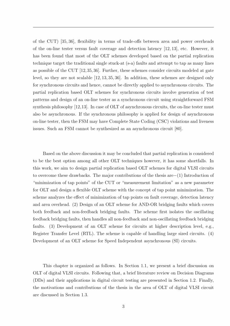
Figure 2.3 requires 233 vectors for exhaustive functional testing. Using structural knowledge
of the system this complexity, however, can be reduced to a great extent. Structural testing,
introduced by Eldred in [38], depends on the specific structure of the circuit involving gate
types, interconnects, fault models, etc. One of the advantages of structural testing is the
ability to develop efficient algorithms to generate the structural test vectors. For example,
by using the information about the structure of the adder (shown in Figure 2.3) and adding
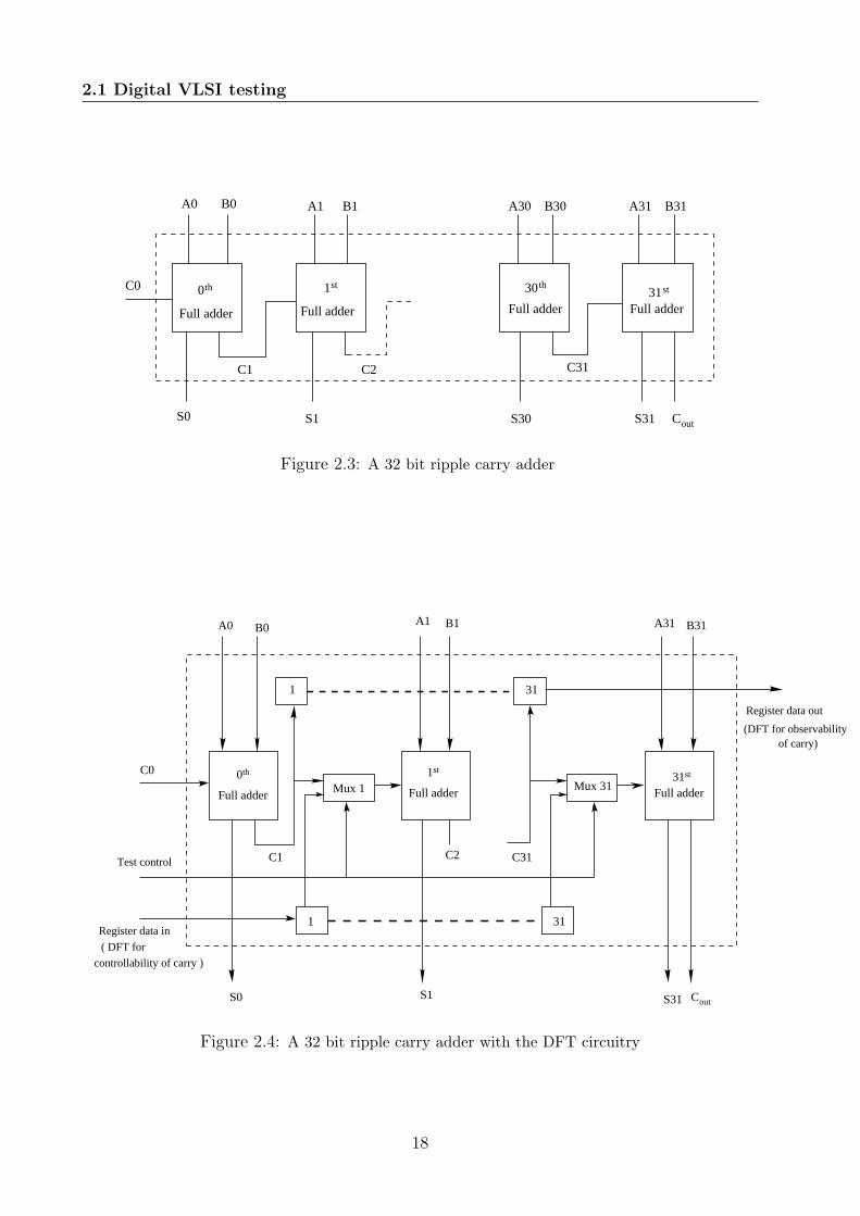
a small amount of additional hardware, it can be tested with 8 test vectors only. The 32 bit
adder with DFT circuitry is shown in Figure 2.4.
It may be noted that in this case, two−31 bit shift registers, and 31 number of 2 : 1
multiplexers comprise the additional DFT circuit. One shift register (called input register)
provides inputs to the “carry input” bits of the individual adders during test and the other
shift register (called output register) latches outputs from the “carry output” bits of the
individual adders. In the modified 32 bit adder, the carry input to the ith (full) adder is
multiplexed with the ith bit of the input shift register, 1 ≤ i ≤ 31. During normal operation
16

2.1 Digital VLSI testing
Table 2.1: Variants of VLSI testing
Criterion Attributes of testing
method
Terminology
When is the test per-
formed?
Concurrently with the normal
system operation
On-line/Concurrent testing
As a separate activity Off-line testing
Where is the source of
stimuli?
Inputs during operation On-line testing
Within the chip Built-In-Self-Test (BIST)
Applied by an external device Automatic Test Equipment
(ATE) based testing
What is tested? Design errors Design verification testing
Fabrication errors Manufacturing test
Failure during operation On-line testing (OLT)
Which physical object
is being tested?
Wafer Non packaged ICs level testing
IC Packaged level testing
Board Board level testing
System System level testing
How are the stimuli ap-
plied?
In a fixed predetermined order Static Testing
Depending on results Adaptive testing
How fast are the stim-
uli applied?
Much slower than the normal
speed of operation
DC (static) testing
At normal speed of operation At-speed testing
Who checks the re-
sults?
On-chip circuit Self-checking
External tester External testing
17
2.1 Digital VLSI testing
A0 A1B0 B1 A30 B30 A31 B31
C0
C1 C2 C31
0th
Full adder
1st 30 th31st
Full adder Full adder Full adder
S0 S1 S30 S31 Cout
Figure 2.3: A 32 bit ripple carry adder
1 31
1 31
A0 B0A1 B1 A31 B31
C0 0th
Full adder
1st31st
Full adder Full adderMux 31Mux 1
C1 C31C2
S0 S1 S31 Cout
of carry)
Register data out
(DFT for observability
Test control
Register data in
( DFT for
controllability of carry )
Figure 2.4: A 32 bit ripple carry adder with the DFT circuitry
18

2.1 Digital VLSI testing
of the 32 bit adder, the multiplexers connect the carry input of the ith (full) adder to the
carry output of the (i− 1)th (full) adder, 1 ≤ i ≤ 31. However, during test, the multiplexers
connect the carry input of the ith (full) adder to the output of the ith bit of the input shift
register, 1 ≤ i ≤ 31. The values in the shift register are fed externally. It may be noted that
by this DFT arrangement all the (full) adders can be controlled individually as direct access
is provided to the carry inputs of the adders; inputs other than carry are already controllable.
Hence, testing in this case would be for each (full) adder individually and that requires 8
test vectors as each of the 32 full adders can be tested in parallel. Correct operations of each
of the full adders are determined by looking at the sum and the carry outputs. Sum outputs
are already available externally and hence no DFT circuit is required to make them directly
observable. For the carry outputs, however, another similar DFT arrangement is required to
make them observable externally. This would require the output (31 bit parallel load and)
shift register where the carry output bit of the (i−1)th adder is connected to the ith input of
the output shift register, 1 ≤ i ≤ 31. Once the values of all the carry bits are latched in the
register, which is done in parallel during test, they are shifted out sequentially. In this case
a full adder is tested functionally and structural information is used at the cascade level.
Thus, it may be stated that “structural testing is functional testing at a level lower than
the basic input-output functionality of the system”. In the case of digital circuits, structural
testing is “functional testing at the level of gates and flip-flops”. Structural test vectors aim
to detect manufacturing faults and try to confirm the correctness of the device structures in
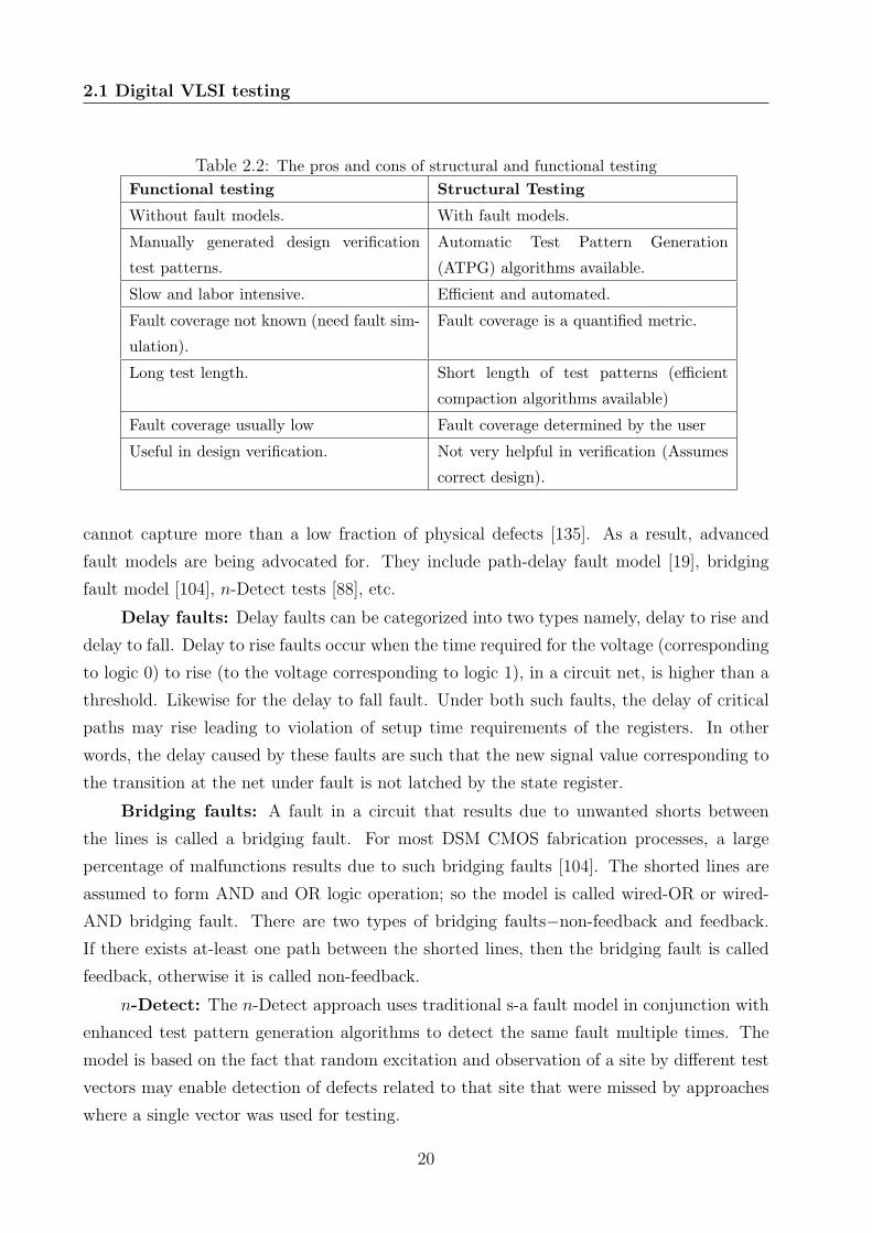
the manufacturing process like wires, flip-flops and gates. The pros and cons of structural
and functional testing are shown in Table 2.2.
2.1.2 Fault models
Central to the advantages of structural testing are the fault models. At the physical level
an enormous number of different faults could be present and it is quite complex to analyze
them at that level. Thus, physical level faults are grouped together with regard to their
manifestation at the logic functionality of the circuit, which are termed as fault models
[2, 17]. A fault model facilitates the identification of targets for testing and generation of
input patterns to test the faults in the fault model. The most commonly used fault model is
the single stuck-at (s-a) fault model [2,17]. This is modeled by having a circuit net s-a logic
0 or 1 (i.e., s-a-1 or s-a-0). The number of s-a faults in a circuit is linear with respect to the
number of nets in the circuit netlist; if there are n nets in a circuit, the number of single s-a
faults is O(2n).
With the arrival of deep sub-micron designs, it is found that the single s-a fault model
19
2.1 Digital VLSI testing
Table 2.2: The pros and cons of structural and functional testing
Functional testing Structural Testing
Without fault models. With fault models.
Manually generated design verification
test patterns.
Automatic Test Pattern Generation
(ATPG) algorithms available.
Slow and labor intensive. Efficient and automated.
Fault coverage not known (need fault sim-
ulation).
Fault coverage is a quantified metric.
Long test length. Short length of test patterns (efficient
compaction algorithms available)
Fault coverage usually low Fault coverage determined by the user
Useful in design verification. Not very helpful in verification (Assumes
correct design).
cannot capture more than a low fraction of physical defects [135]. As a result, advanced
fault models are being advocated for. They include path-delay fault model [19], bridging
fault model [104], n-Detect tests [88], etc.
Delay faults: Delay faults can be categorized into two types namely, delay to rise and
delay to fall. Delay to rise faults occur when the time required for the voltage (corresponding
to logic 0) to rise (to the voltage corresponding to logic 1), in a circuit net, is higher than a
threshold. Likewise for the delay to fall fault. Under both such faults, the delay of critical
paths may rise leading to violation of setup time requirements of the registers. In other
words, the delay caused by these faults are such that the new signal value corresponding to
the transition at the net under fault is not latched by the state register.
Bridging faults: A fault in a circuit that results due to unwanted shorts between
the lines is called a bridging fault. For most DSM CMOS fabrication processes, a large
percentage of malfunctions results due to such bridging faults [104]. The shorted lines are
assumed to form AND and OR logic operation; so the model is called wired-OR or wired-
AND bridging fault. There are two types of bridging faults−non-feedback and feedback.
If there exists at-least one path between the shorted lines, then the bridging fault is called
feedback, otherwise it is called non-feedback.
n-Detect: The n-Detect approach uses traditional s-a fault model in conjunction with
enhanced test pattern generation algorithms to detect the same fault multiple times. The
model is based on the fact that random excitation and observation of a site by different test
vectors may enable detection of defects related to that site that were missed by approaches
where a single vector was used for testing.
20

2.1 Digital VLSI testing
2.1.3 Test programming
The test program development consists of two broad steps−(i) generation of test vectors
and (ii) generation of the corresponding golden responses for a fault free circuit. Figure 2.5
shows the basic steps of a test program generation.
Architecture specs. Logic design
Physical design
generator
Test program
Test program
logic synthesisHigh level synthesis and
Fault coverageFault modelTest types
Testpatterns
Placement and routing
Pin assignments
Figure 2.5: Basic steps in test program generation
Test pattern generation
It involves generation of a minimal subset of input patterns, such that all faults of the
considered fault model are sensitized and their effects are propagated to the output. The
process of test pattern generation can be divided into two distinct phases; 1) test generation
and 2) test application.
For (1), appropriate circuit model (e.g., gate level model) and fault model (e.g., s-a fault
model) are to be identified. Construction of a test pattern for a fault comprises determining
an input pattern such that the output obtained from the circuit with the fault is different
from that of the fault free circuit. As test patterns are to be generated for all faults, this
approach can be computationally expensive, however, it is performed off-line and only once
after the design stage. On the other hand, for (2), all test patterns are to be applied to
21

2.1 Digital VLSI testing
each integrated circuit manufactured which may be millions in number; thus, the test set
generated must be efficient in terms of the time required for application to the circuits.
An overview of the algorithms used for test pattern generation is as follows. An ATPG
algorithm basically comprises three steps:
• Fault propagation: Select a line from the point of occurrence of the fault to the Circuit
Under Test (CUT) output that would be used to manifest the effect of the fault. The
inputs of all the gates falling in that path other than the one through which the fault
is to be propagated are to be driven to their non-controlling values; for example, if a
two input OR gate, having inputs X and Y , is in the fault propagation path and input
X is the line through which the fault is to be propagated to the output, then Y is to
be set to 0; a dual of this step is applicable for an AND gate.
• Fault sensitization: Assume a value at the fault site that is opposite of the fault to be
detected; in other words, if a s-a-1 is to be detected at net A, then assume a signal
value 0 at A.
• Line justification: Determine if an input pattern exists such that the assumed value at
net A is attained and the path from net A to the output is sensitized.
The same technique can be applied to a sequential circuit, but before that the sequential
elements of the circuit are explicitly driven to a required state using scan based DFT circuitry
[2, 17]. The well known ATPG algorithms are D-algorithm, PODEM and FAN [2,17,133].
Output response analysis
ATPG algorithms also provide the expected output response from the fault free CUT (for a
given test). The test data obtained from the CUT is compared with the expected response
and consequently, the comparison mainly serves two purposes. First, it helps to accept or
reject the CUT. Secondly, the mismatch of output due to fault can be used for “fault mode
analysis” which provides diagnostic information for improving the design, fabrication and
test flow for the subsequent design iterations.
2.1.4 Comparison of ATE based testing, BIST and OLT
VLSI testing can be broadly classified into the following three major categories on the basis
of the phase (manufacturing, startup or on-line) during which the test is performed:
22

2.1 Digital VLSI testing
1. ATE based testing: This involves testing the circuit using Automatic Test
Equipment (ATE) just after manufacturing. In this class of testing, test patterns are
applied to a circuit and outputs are compared with the expected fault free responses
using off-chip equipments [79, 90, 127]. Generally speaking, there is a difficulty in at-
speed testing because the operational speed of modern day VLSI circuits is higher than
that of an ATE. Since testing of a circuit using ATE is performed once just after its
manufacturing, thus, the faults that develop after deployment of the circuit cannot be
detected. So ATE based testing is according termed as off-line testing. Further, the
cost of ATE based testing is high because of the price of its individual components.
2. Built-In-Self-Test (BIST):Due to the steep increase in complexity of digital circuits,
BIST has been realized in many designs to implement some of the test functions on-
chip [8, 33, 42]. Compared to off-line testing, the advantage of BIST is that it enables
reduction in the demands on the external ATE, thus enabling at-speed and in-situ
testing. This permits the scheme to test circuits every time they are powered ON, even
after they are deployed in the system. The basic BIST components are the Test Pattern
Generator (TPG), the Test Response Evaluation (TRE) unit and the Test Controller
(TC) [17]. At the circuit level, the inputs have to be preceded by a multiplexer to
connect either to the normal (functional) inputs or the outputs of the test pattern
generator. TPG, TRE and multiplexer are controlled by the TC. Figure 2.6 illustrates
the basic architecture of a circuit with BIST.
On−
chip
patte
rn
gene
rato
r
On−
chip
re
spon
se
anal
yzer
(M
ISR
)
Test controller
MUX Circuit Under Test(CUT)
Data from system Data to system
Status(pass/fail)
Figure 2.6: BIST scheme
3. On-line Testing (OLT):
It has been observed that as the scale of integration increases, the operation of the
Integrated Circuits (ICs) are becoming increasingly susceptible to faults that are absent
23

2.2 Literature review: On-line testing of digital VLSI circuits
during fabrication or power up but develop on-the-fly [37, 84]. Off-line test strategies
(like ATE based testing, BIST, etc.) need to withdraw the circuit from normal
operation for testing, which may not be always permissible. Immediate detection of
the faults that occur on-the-fly during operation of the circuit requires incorporation
of a technique which will continuously observe its operation by checking whether the
response follows its normal behavior. These techniques fall under the category of OLT
[47, 83, 84, 89]. OLT (also called concurrent testing) can be defined as a technique to
monitor a circuit and detect the occurrence of a faut (from the fault model) within a
finite time of its occurrence. Unlike off-line testing (involving ATE based testing and
BIST), where test vectors can be applied, either through external test equipments or
on-chip pattern generators, OLT requires that the circuit contains some DFT circuitry
to test itself for all the vectors that it encounters during its normal mode of operation.
Thus, in OLT, neither can patterns be applied from a test circuit/pattern generator
nor can the memory elements (registers) be separated from the core. In other words,
unlike off-line testing, there is no “test mode” in OLT, where the circuit operation
can be altered for testing. There are four primary parameters to be considered in the
design of an OLT scheme:
(a) Fault coverage: The fraction of all modeled faults that are detected; it is usually
expressed in percentage.
(b) Fault detection latency: The number of clock cycles that may be required for the
detection of a fault after a deviation from the normal behaviour is observed for
the first time.
(c) Area overhead: The extra amount of on-chip hardware needed to perform OLT,
i.e., area of the on-line tester circuit.
(d) Power overhead: The extra power needed to perform OLT.
Tables 2.1.4, 2.1.4 and 2.1.4 compare these three major test paradigms to bring forth
their advantages and disadvantages.
2.2 Literature review: On-line testing of digital VLSI
circuits
In this section we provide a survey highlighting the works reported in the literature on OLT
of digital circuits. Further, the pros and cons of each of the test methodologies are also
24

2.2 Literature review: On-line testing of digital VLSI circuits
Table 2.3: Merits and demerits of ATE based off-line structural testing [2, 17]
Merits Demerits
• Low complexity of ATPG algorithms.
• On-chip hardware overhead: 5 to 10%
of core area.
• Automated flow: Well-established
CAD tool support for scan based DFT
and ATPG.
• Difficulty in at-speed testing:
– ATE speed is in MHz range while
operational VLSI core speed
may be several GHz.
• Converts sequential circuits to virtual
combinational ones using scan chains.
– Changes the core delay charac-
teristics.
– Requires a non-operational
mode for testing: OLT is not
supported.
• Dead load of test equipments
– Difficulty in in-situ testing.
discussed. OLT techniques for digital VLSI circuits (both combinational and sequential),
reported in literature, can be classified into the following main categories:
1. Signature monitoring in Finite State Machines (FSMs)
2. Self-checking design
3. Partial replication
4. On-line BIST
2.2.1 Signature monitoring in FSMs
Signature monitoring techniques for OLT basically work by studying the state sequences
of the FSM model of a sequential circuit during its operation. Signatures are FSM
state sequences traversed during execution. In these methods, signatures are analyzed
concurrently with the execution of the circuit. This analysis targets to detect faults leading
25

2.2 Literature review: On-line testing of digital VLSI circuits
Table 2.4: Merits and demerits of BIST
Merits Demerits
• Reduced parasitics, loading, etc. due
to absence of ATE, probes, packaging,
etc.
• Reduced test point access problem.
• Startup, at-speed and in-situ testing
supported.
• High on-chip hardware overhead when
compared to ATE based testing.
• On-chip BIST hardware design com-
plexity
– Signal application.
– Signal tapping.
– Test evaluation.
• Test of BIST hardware.
• Cannot detect faults that develop on
the fly.
• CAD tools for automated BIST circuit
design are rare or application specific.
• On-chip power consumption
Table 2.5: Merits and demerits of OLT
Merits Demerits
• All advantages of BIST holds.
• On-line detection of faults is possible
avoiding suspension of normal opera-
tion.
• Area and power overhead of the OLT
circuit.
• On-chip tester area overhead is higher
compared to area requirements of
BIST.
• Testing of the OLT circuit.
• No CAD tool for generating on-line
test circuits is widely accepted or
available commercially.
26

2.2 Literature review: On-line testing of digital VLSI circuits
to illegal paths in the control flow graph, i.e., paths having transitions which do not exist in
the FSM specification. To ensure that the runtime signature of the fault free FSM is different
from the one with fault, a signature invariant property is forced during FSM synthesis. The
principle of signature monitoring for FSMs has been proposed in [66,67]. Figure 2.7 illustrates
the basic architecture for OLT using the scheme of signature monitoring in FSMs. The main
component of the monitor is a Multiple Input Shift Register (MISR), which generates a
signature using the polynomial division of the codes of the state that is reached during
normal operation. So the runtime signature represents a value of the path followed through
the control-flow graph of the FSM. A primitive polynomial is used to perform division in order
to reduce the fault masking (also called “aliasing”). The correct values of the signature are
pre-computed from the specified FSM graph and are compared with the runtime signature
at some special states called checking points. To ensure that the runtime signature of the
normal circuit FSM is different from the faulty one, an invariant property is forced during
FSM synthesis and can be stated as [67]:
Signature invariance property: The signature of the sequence of state codes
obtained by polynomial division with the primitive divisor polynomial is invariant after
each state in the graph, when any legal path is taken. Checking involves comparison of the
runtime signature with the invariant reference signature when the current state corresponds
to any selected check points. To obtain an FSM with signature invariance property the
state assignment procedure is modified to take into account the constraints related to
such an invariance. The approach has been proved to be feasible in [66, 67] and several
implementations based on this approach have been reported in [22,100,115].
The major advantage of the schemes based on signature monitoring is due to the fact
that the area overhead incurred for OLT is extremely low (and almost negligible in cases
of FSMs with large number of states); the results presented in [67] has reported that the
area of the additional circuit required for OLT is about 1% to 5% of the CUT when the
FSM is large. It is also discussed in [67] that detection latency may be high for some FSMs
which can be remedied by increasing the number of checkpoints, however, incurring more
area overhead. The hybrid signature monitoring scheme reported in [22] detects control
flow errors caused by transient and intermittent faults. It is shown that the scheme has
offered very high fault coverage with low detection latency and area overhead. In [115], a
concurrent control flow error detection and recovery mechanism has been proposed using
encoded signature monitoring technique. The scheme recovers from most of the control flow
errors with relatively low performance overhead.
However, many times by default, signature invariance is not present. In that case, the
27

2.2 Literature review: On-line testing of digital VLSI circuits
functionNext state
Output
logic
Stateregister
MISR
logicReference
signal
ComparatorPO
PI
Status
FSM for the circuit Signature monitor
Comparison
Figure 2.7: Basic architecture for signature monitoring
state assignment procedure of the FSM may have to be modified to take into account the
constraints related to such an invariance. In other words, signature monitoring techniques
for OLT require some special properties in the circuit structure, so they require re-synthesis
and re-design, which lead to a change in the original structure of the circuit; they are
accordingly termed as intrusive OLT methodologies. In the worst case, when the FSM
graph is well connected, a large number of new states are added to achieve the signature
invariant properly. Further, the state explosion problem in FSM makes the application of
this scheme difficult for practical circuits; results reported in the OLT literature using these
schemes are limited to circuits having typically about one hundred states.
2.2.2 Self-checking design using error detecting codes
The basic principle for self-checking design using error detecting codes is as follows. Let the
Circuit Under Test (CUT) realize a Boolean function f . The OLT scheme contains another
module called output characteristic predictor, which predicts some special characteristic of
the CUT output f(i) for the input i, independently. Finally, the checker verifies whether the
special characteristic of the output which is produced by the CUT in response to input i is
same as the predicated one. If there is any mismatch found, then an error signal is produced.
Some examples of the characteristic of f(i) (for self-checking using error detecting codes) are
28

2.2 Literature review: On-line testing of digital VLSI circuits
parity of f(i), 1’s count in f(i), etc. The basic self-checking design scheme discussed above
is depicted in Figure 2.8.
CUT
function f
characteristicpredictor
Output
PO
Error
Predictedoutput characteristic
Checkerindication
PIi
Figure 2.8: Basic architecture for self-checking circuit
The technique of OLT using self-checking circuits based on error detecting codes was
motivated from the error detection and correction techniques used in communication. The
CUT output (or information) bits are augmented with some additional bits, called check
bits (using an additional logic), such that under normal condition of the CUT and the
additional logic, the CUT output augmented with the check bits is a code word of the error
detecting code chosen. The checker verifies whether the CUT output augmented with the
check bits is a code word of the error detecting code chosen. The effect of a fault in the CUT
leading to change in some output bit is called an error. The above mentioned technique
can be easily used for sequential circuits [53, 118] where the CUT illustrated in Figure 2.8
is the next state function of the sequential circuit. The circuit corresponding to the output
characteristic predictor feeds additional flip-flops (other than the ones in the original circuit).
Thus, the outputs of circuit flip-flops augmented with that of the additional flip-flops is a
code word of the error detecting code chosen. The checker taps the outputs of these flip-flops
taken together. The basic self-checking design scheme for sequential circuits is depicted in
Figure 2.9.
Before we move on to presenting the most important error detecting codes, we define
some fundamental terms used in the context of self-checking circuits; they can be found in
almost every publication addressing self-checking designs [14,53].
Self-testing circuit: A circuit is self-testing, if for every fault in the specified fault model,
there is an input that produces a non-code output.
Fault-secure circuits: A circuit is fault-secure, if an input can produce a non-code word
or a correct code word. That is, they cannot be incorrect code words.
29
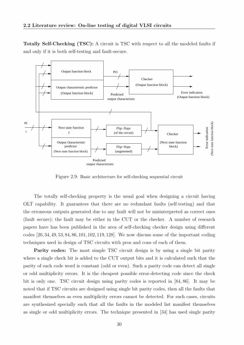
2.2 Literature review: On-line testing of digital VLSI circuits
Totally Self-Checking (TSC): A circuit is TSC with respect to all the modeled faults if
and only if it is both self-testing and fault-secure.
Output function block
(Output function block)
Output characteristic predictor
Checker
(Output function block)
Next state function
f
Output characteristic
(Next state function block)
predictor
(of the circuit)Flip−flops
Flip−flops(augmented)
Checker
(Next state function block) E
rror
indi
catio
n
(Nex
t sta
te fu
nctio
n bl
ock)
PO
PI
Error indication(Output function block)
Predicted output characteristic
i
Predicted output characteristic
Figure 2.9: Basic architecture for self-checking sequential circuit
The totally self-checking property is the usual goal when designing a circuit having
OLT capability. It guarantees that there are no redundant faults (self-testing) and that
the erroneous outputs generated due to any fault will not be misinterpreted as correct ones
(fault secure); the fault may be either in the CUT or the checker. A number of research
papers have has been published in the area of self-checking checker design using different
codes [20, 34, 49, 53, 84, 86, 101, 102, 119, 128]. We now discuss some of the important coding
techniques used in design of TSC circuits with pros and cons of each of them.
Parity codes: The most simple TSC circuit design is by using a single bit parity
where a single check bit is added to the CUT output bits and it is calculated such that the
parity of each code word is constant (odd or even). Such a parity code can detect all single
or odd multiplicity errors. It is the cheapest possible error-detecting code since the check
bit is only one. TSC circuit design using parity codes is reported in [84, 86]. It may be
noted that if TSC circuits are designed using single bit parity codes, then all the faults that
manifest themselves as even multiplicity errors cannot be detected. For such cases, circuits
are synthesized specially such that all the faults in the modeled list manifest themselves
as single or odd multiplicity errors. The technique presented in [34] has used single parity
30

2.2 Literature review: On-line testing of digital VLSI circuits
bit for the entire circuit. To limit the scope of fault manifestation, each primary output is
synthesized independently and so there is no sharing of logic gates among any pair of output
bits. As a result, faults in any block can imply at most one output error. The single bit
parity technique mandates no logic sharing among any two outputs. So it may result in high
area overhead for some circuits. In order to reduce area overhead, the multiple-parity-group
technique was introduced in [39, 119] that allows logic sharing among some outputs. This
technique partitions the primary outputs into different parity groups. It was shown that
logic sharing can be allowed among the outputs that correspond to different parity groups
and that would still result in faults changing only a single output bit. The outputs of the
same parity group are verified using a TSC parity checker.
m-out-of-n codes: An m-out-of-n code word has exactly m 1s out of total n bits.
m-out-of-n code is an unordered code i.e., no two code words x and y are present such that
x has 1 in every bit position where y has a 1. An example of m-out-of-n code for TSC
circuit design can be found in [20]. Simple inspection of the results presented is enough to
illustrate the complexity of checkers based on such unordered codes compared to a parity
checker. They were not widely adopted since they are much more expensive to implement
than parity based schemes.
Berger codes: A Berger code consists of an information part and a check part, which is
the binary representation of the number of 1s in the information part. So, it is an unordered
code. TCS circuits using this methodology can be found in [21, 112]. Area overheads of
the self-checking circuits designed using Berger codes are higher compared to ones designed
using parity based schemes.
As a practical application, the residue code technique is used in [49] for design of self
checking modulo multiplier, which is used in various cryptographic systems. In another work
[128], D. P. Vasudevan and P. K. Lala have proposed a new approach for designing of self
checking carry select adder of arbitrary size and the adder can detect both permanent and
transient s-a faults on-line. The area overhead for making circuits totally self checkable is
usually not high. A number of design and synthesis constraints are, however, required by
the coding technique based methodologies to control the scope of fault propagation. For
example, the method reported in [53] requires that all inverters be pushed to the primary
inputs and for the scheme proposed in [34] there should be no logic sharing within a single
parity group. Since these techniques require some special properties in the circuit structure,
they require re-synthesis and re-design. So, OLT schemes based on design of TSC circuits
using coding theory are intrusive in nature.
To address the issue of intrusiveness of coding theory based OLT schemes, weight based
31

2.2 Literature review: On-line testing of digital VLSI circuits
codes are used [31], where a weight is assigned to each output (information) bit and the sum
of weights of the output (information) bits, which have value 1, represent the check bits.
Weight-based codes can distinguish between errors changing output bits from 1 to 0 and
from 0 to 1, because both these errors result in a different weight. So they do not require
any special synthesis constraints to restrict the fault manifestation. Further, such codes
are positional ones, i.e., the check bits are a function of the erroneous bits as well as their
positions in the output (which is determined by the individual weights assigned to the output
bits). Thus, they can have high fault detection capabilities. The only drawback of using
weight based codes is the high area overhead compared to Berger, parity orm-out-of-n codes.
2.2.3 Duplication schemes for OLT
XOR based comparator
Module 2Module 1
Input data
Status
Figure 2.10: Basic architecture for duplication based OLT
One of the most straightforward way of designing systems with OLT capability is
duplicating itself and crosschecking for similarity of the output responses. The basic
duplication scheme is presented in Figure 2.10. Module 1 and Module 2 are functionally
equivalent, that is, they operate identically (in the fault free case) and produce the same
outputs when fed with the same inputs. If they are structurally equivalent as well (i.e., their
gates and interconnections are identical), then the technique is called identical duplication.
Otherwise, it is a diverse duplication technique. Duplication schemes are fault secure by their
very nature. However, hardware overhead of more than 100% is introduced in the design if
every module is physically duplicated [84]. In [76], Mitra et al. have compared identical and
32

2.2 Literature review: On-line testing of digital VLSI circuits
diverse duplications with respect to their vulnerabilities to fault pairs; their simulation results
are in favour of the diverse case. An interesting alternative to full hardware duplication is
presented in [116], where Module 2 (Figure 2.10) is replaced by a minimized version of
Module 1 (i.e, CUT), such that all targeted faults can be detected eventually. Further, the
comparator is equipped with a (simple) test control unit that specifies if the checker must
check or not, depending on the input word. So, it becomes a controllable comparator/checker.
This technique is termed as “partial replication”. The main advantages of partial replication
technique are due to its non-intrusiveness, low area overhead and flexibility in terms of trade-
offs between area overhead versus fault coverage and detection latency.
A number of OLT schemes based on partial replication have been proposed by Drineas
et al. [35,36], where a complete set of test vectors is obtained using standard Automatic Test
Pattern Generation (ATPG) on the next state logic of the CUT, considering the current state
bits also as inputs. Then a subset of the test vectors is taken and synthesized into a partially
replicated circuit that generates the expected next state of the CUT when an input-present
state combination matches with a test vector. The partially replicated circuit outputs are
compared with state flip-flop outputs of the CUT and in case of a mismatch, a fault indicator
bit is set. The input-present state combinations that are not considered in the test vector
subset are treated as don’t cares and this results in the partially replicated circuit having
lower area when compared to the next state logic of the CUT. The efficiency of these schemes
[35,36] strongly depends on the prior knowledge regarding the input patterns that the CUT
is likely to receive. To elaborate, the patterns (test vectors) that occur frequently should
be included in the subset for construction of the partially replicated tester and others that
occur rarely may not be considered. Further, since ATPG algorithms generally reveal one
test pattern for a given fault, they must be executed a multiple number of times to generate
a complete (or large) set of test vectors. In case of practical circuits, the use of ATPG
algorithms may become prohibitively complex, as OLT requires the exhaustive set (or a
large subset) of test vectors. Since these schemes reported in [35, 36] use standard ATPG
algorithms for generation of test vectors, they are not scalable. Results have been reported
for circuits up to 64 states and 3 inputs only.
Biswas et al. [10–12] have proposed a series of partial replication based OLT schemes
for s-a faults. These techniques are non-intrusive in nature, flexible in terms of area overhead
versus fault coverage and detection latency, and scalable up to circuits having ten thousand
gates and five hundred filp flops. The complexity of generation of test patterns of the CUT
is addressed by using Ordered Binary Decision Diagram (OBDD). The complete set of test
patterns is generated from the OBDD representation of the CUT and on-line tester circuit
33

2.2 Literature review: On-line testing of digital VLSI circuits
is designed using a subset of these test patterns. The steps involved for generation of test
patterns are−i) representing each output of the CUT using separate OBDDs under normal
and faulty conditions, ii) performing XOR operation between normal and faulty OBDDs and
constructing XORed OBDD, iii) applying “satisfy-all-1” on the XORed OBDD. Application
of OBDD enables the proposed scheme to handle fairly complex circuits.
It is seen that most of the partial replication based OLT schemes reported in the
literature work for single s-a faults [10–12,35,36]. However, in modern integration technology,
single s-a fault model can capture only a small fraction of real defects and as a remedy,
advanced fault models such as bridging faults, transition faults, delay faults, etc. are
considered. Biswas et al. have extended the approach reported in [12] for bridging faults
and delay faults in papers [13] and [9], respectively. However, in case of bridging faults the
authors have considered only non-feedback bridging faults and ignored the feedback bridging
faults as they create oscillations. Further, all the OLT schemes based on partial replication
technique [9–13, 35, 36] consider the circuits modeled at gate level, hence these are scalable
only up to certain extent. Also, these schemes are designed only for synchronous circuits, so
they cannot be directly applied to asynchronous circuits. Another assumption is regarding
the tapping of lines of the CUT by the on-line tester. All the existing works on on-line
tester design tap as many lines as possible of the CUT because the on-line tester circuit is
fabricated on the same chip with the CUT and any point of the CUT can be tapped easily.
However, it is known that tapping of lines of any circuit results in increase of load (fanouts)
on the gates which drive the tap points. To handle the increased load extra buffers are
required, which increase the area of the circuit. So if the on-line tester is designed with more
number of tapings in the CUT, it results in large area overhead.
2.2.4 On-line BIST
As discussed in Subsection 2.1.4, the scheme used for design of circuits with additional on-
chip logic, which can be used to test the circuit every time before it starts up, is termed
as off-line BIST. Off-line BIST resources can also be utilized for OLT [7, 82, 113, 130, 131].
This technique performs on-line BIST by utilizing the idle times of the various modules of
the circuit during normal operation. Thus, this is the only technique that facilitates both
on-line and off-line testing using the same on-chip resources. As the feasibility and efficiency
of this scheme depends on the idle times of the circuit modules, it may not be applicable to
modern day circuits. This is because, such circuits are designed to achieve parallelism and
pipelining by reducing the idle times of the circuit modules.
34

2.3 Desired features of OLT schemes
2.2.5 Pros and cons of different OLT techniques
We have discussed four broad classes of OLT techniques with their advantages and
disadvantages in Subsections 2.2.1, 2.2.2, 2.2.3 and 2.2.4. Table 2.6 shows the important
pros and cons of these OLT techniques in brief. Based on the observations in Table 2.6, it
can be stated that partial replication technique is the best among others. However, many
issues still remain to be solved in partial replication based OLT schemes and some of the
prominent ones are as follows:
• Measurement limitation based flexibility: The on-line testers should provide
flexibility in terms of trade-offs between measurement limitation (reduction in number
of tap points) versus area overhead, fault coverage and detection latency.
• Coverage for advanced fault models: Designing OLT schemes that support fault
models appropriate for the latest VLSI design paradigm, e.g., bridging faults including
feedback, delay faults, transition faults, etc.
• Scalability: The on-line tester design algorithms should be capable of handling large
size circuits.
• Handling asynchronous circuits: Developing OLT schemes that are applicable for
asynchronous circuits.
There are very few works that have been proposed to address these problems. In
the next section, we review elaborately the existing works in these areas, following that,
motivation of the thesis is discussed.
2.3 Desired features of OLT schemes
2.3.1 Measurement limitation based flexibility in OLT
In OLT, a tester circuit is designed using a subset of test patterns and it checks the response
of the circuit against each of the patterns in the subset and detects if there is any deviation
from the normal responses. The area and power overheads of an OLT scheme depend on the
number of test patterns considered in the design of the on-line tester circuit. There are two
possible approaches to reduce the area and power overheads of the on-line tester. First one
is, by dropping some of the test patterns in the on-line tester design, however, it increases
the fault detection latency. Second one is, by not considering some faults in the on-line tester
design, however, it reduces the fault coverage. Similarly, the power overhead can be reduced
35

2.3 Desired features of OLT schemes
Table 2.6: Pros and Cons of different OLT techniques
OLT techniques Pros Cons
Signature monitoring Low area overhead Intrusiveness
in FSMs
State explosion problem in FSMs
Applicable for small circuits
High fault detection latency
Self-checking design Low area overhead Intrusiveness
Low fault coverage
Partial replication Simplicity in design, Area overhead is more than 100%
(under full duplication)
Maximum possible tap points
(full measurement)
Supports non-feedback Mainly applied for
bridging faults, stuck-at faults
Facilitates trade-offs Works at gate level,
between area overhead hence non-scalable
versus fault coverage
and detection latency,
Non-intrusiveness. Designed for
synchronous circuits
On-line BIST Provides both on-line Depends on idle time of
and off-line testing with a circuit modules
single on-chip tester. High fault detection latency
by selecting test patterns such that the number of switchings between any two test patterns
is less. Thus, flexibility in OLT schemes can be achieved through trade-offs between area and
power overhead of the tester versus fault coverage and detection latency. The OLT schemes
reported in [9, 12, 13] provide flexibility in terms of trade-offs between area overhead versus
fault coverage and detection latency by selecting a subset of the test patterns. These works
have shown that the area overhead can be lowered by considering a subset of test patterns
for on-line tester construction. However, the subset is selected in a fashion such that for all
faults, at-least one test pattern is present. It is also shown that the impact of lowering the
test patterns is almost linear with the detection latency [9,12,13]. In [12], the authors have
developed an OLT scheme using state based model for s-a faults and this scheme is extended
36

2.3 Desired features of OLT schemes
for non-feedback bridging faults and delay faults in [13] and [9], respectively.
The on-line tester circuit is placed on-chip with the Circuit Under Test (CUT). The
tester taps certain lines of the CUT, whose values are used to determine whether any fault
has developed in the CUT. Such tap points are analogous to sensors used in physical systems
[62]. Unlike physical systems, where sensors cannot be placed at all desired locations, in case
of circuits the on-line tester can tap any point of the CUT. So, all the above mentioned OLT
schemes (Section 2.2.3) have emphasized on keeping the scheme as non-intrusive as possible,
totally self-checking, low area overhead, high fault coverage, low detection latency, etc., but
ignored the issue of tap points. However, tapping of lines of a CUT results in increase of
load (fan-outs) on the gates which drive the tap points [63]. Such increase in load requires
use of additional buffers that increase area overhead. So, if the concept of fault detection
under measurement limitation (i.e., sensor placement limitation in case of physical system
[85, 114]) is applied for OLT of circuits, we can minimize the tap points of the CUT and
reduce the number of driving buffers. This will minimize the area overhead of the tester.
However, minimization of tap points also compromise fault coverage and detection latency.
So, number of tap points can be considered as a new design parameter to provide trade-offs
between area overhead versus fault coverage and detection latency.
In this thesis, we develop a partial replication based OLT scheme for s-a faults with
the concept of tap point reduction and analyze the affect of this reduction on fault coverage,
detection latency and area overhead.
2.3.2 OLT schemes for advanced fault model
With the arrival of DSM designs it is observed that the single s-a fault model cannot capture
more than a fraction of the real defects [135]. In view of this some initial efforts have been
given for the design of circuits having OLT facility for advanced fault models. The number of
such OLT schemes is few and most of them are based on the bridging fault model. Broadly
speaking, if two normally distinct points (lines) are shorted together in a circuit, then the
situation is called bridging fault. The shorted lines are assumed to form AND and OR logic
operation; so the model is called wired-OR and wired-AND bridging fault. Bridging faults
can be divided into two types (i) simple bridging fault or non-feedback bridging fault and
(ii) feedback bridging fault. If there exist at-least one path between the two shorted lines,
then the bridging fault is called feedback bridging fault, otherwise it is called non-feedback
bridging fault. Now, we present a literature review on different OLT schemes for the bridging
fault model.
OLT for bridging faults was first attempted in [73]. This scheme is based on self-
37

2.3 Desired features of OLT schemes
checking design, where the outputs are encoded with error detecting codes and presence
of any bridging-fault would result in an output which is a non-code word. There are two
major issues with the work, namely (i) inherently the methodology is intrusive and (ii) only
non-feedback faults are considered. As already discussed, the basic idea of self-checking
design comprises imposing some special structure in the circuit so that any fault (from the
fault model considered) results in an non-code word as output, which leads its detection
[53]. Further, the circuit would never produce a wrong codeword as output. To maintain
the self-checking property, several design constraints are imposed during circuit synthesis
making the scheme intrusive. Only non-feedback bridging faults are considered because in
self checking design, effects of the faults need to be mapped to non-code words and if a fault
causes oscillations such mappings are infeasible [73].
Biswas et al. in [13] have developed a partial replication based OLT scheme for bridging
faults. Experimental results in this work illustrated an interesting fact that area overhead
for OLT of bridging faults is not higher compared to that of s-a faults. The major reason
is, a test pattern that detects a bridging fault also detects a s-a fault, but the reverse may
not hold. So, while selecting the partial set of test patterns, only those which can detect
some bridging fault are considered. Using this procedure, low detection latency and high
fault coverage could be achieved for bridging faults, even at low area overheads. The tester
inherently built for bridging faults also provided high fault coverage for s-a faults. However,
again, only non-feedback bridging faults were considered in [13].
Das et al. in [32] attempted to test feedback bridging faults on-line in cluster based
FPGAs. OLT is performed by comparing the outputs (for specific input test pattern
sequence) of the FPGA block under test with golden response using an output response
analyzer. For input cases, when the block under test does not cause oscillations, presence
of fault can be easily tested by comparing responses. However, for other inputs there may
be oscillations, to avoid which, an asynchronous circuit called Muller-C element is used in
all the FPGA blocks. As Muller-C element is adaptable to delay variation, its presence
helps in preventing the circuit to go into oscillation. Although the work was more of a
proof of concept and tried on FPGA, it can be applied by suitable adaption to ASIC based
implementation as well. However, there are two main issues with this approach namely,
intrusivity of the design and use of asynchronous elements. It may be noted that design of
asynchronous testers for OLT of synchronous circuits is not desirable.
Based on the above literature review, in this thesis we propose a synchronous partial
replication based OLT scheme for wired AND-OR bridging faults. The scheme first
determines the bridging faults which do not lead to oscillations, i.e., all non-feedback and
38

2.3 Desired features of OLT schemes
some feedback bridging faults. Following that, exhaustive set of test patterns for these faults
are generated. Also, it is checked if there are patterns, even in case of oscillating feedback
bridging faults, which can detect these faults without oscillations. All these test patterns
taken together are used to design the on-line tester, called FN -detector (Fault versus Normal
condition detector).
2.3.3 OLT schemes for circuits at higher description level
It has been observed that the partial replication based OLT schemes [9,12] at gate level satisfy
almost all efficient parameters of OLT, i.e., non-intrusive, architecture independent, low area
and power overheads, low detection latency, etc. However, these schemes are not scalable to
handle large circuits because they work at gate level and the test pattern generation time
of these schemes are quite high even for moderate sized circuits. So, testing at gate level
becomes a complicated and time consuming task for complex circuits. To overcome this
problem, researchers are interested to test the circuits at higher level of abstraction using
high level fault models. However, testing at higher level is a challenging task due to lack
of well accepted fault models, unlike at the gate level, where single s-a fault model is well
accepted. But it is verified that there exists good correlation between high level fault models
and gate level fault models [25, 94], further gate level fault models have good correlation
with physical defects. So, there exists indirect mapping between high level fault models
and physical defects [133]. Since testing at lower levels (say gate level) using lower level
fault models (say stuck-at-fault model) is scalable only up to certain extent (about 30K
gates and 500 flip flops), so high level fault models are used to test the circuits at higher
abstraction levels. In other words, even though gate level fault models are highly correlated
to real defects, they are not scalable. This difficulty is addressed by developing high level
fault models, testing of circuits using these fault models at higher abstraction levels and
analyzing test quality by indirect mapping of faults versus physical defects [92,97,117].
Now we discuss some high level fault models which are based on behavioral or functional
description of the circuit. These high level fault models are designed to provide good
correlation with the gate level fault models. In [56], Anton Karputkin and Jaan Raik have
proposed a set of behavioral fault models that target detection of stuck at faults in gate level
implementations of the RTL designs. Experiments on a set of ITC’99 benchmarks show that
the proposed fault models achieve high gate level stuck-at fault coverage (average of 86%). F.
Coron et al. [25] proposed an RTL fault model which assumes that all the statements in the
high level description are executed at least once and their fault effects are propagated to the
primary outputs. This fault model captures the single stuck at bit faults on all assignment
39

2.3 Desired features of OLT schemes
statements based on a set of predefined rules. They have achieved a correlation coefficient
about 77% between RTL and gate level fault coverages. The fault model at RTL presented in
paper [59] is based on code validation techniques used in software testing. Results show that
the RTL fault coverage obtained by using this fault model based methodology has a close
match with the gate-level fault coverage. The mixed hierarchical functional fault models
reported in paper [94] are designed to test sequential cores inside the Systems on a Chip
(SoC). The fault models proposed in this paper, based on combination of hierarchical and
functional fault models provide high fault coverage for sequential circuits. It is shown by
experiments that these fault models cover more than 90% of gate-level stuck-at faults for
testing of sequential cores.
Since last decade, a number of high level testing schemes have been proposed using
different high level fault models. Among them the number of OLT schemes is very few
compared to off-line mode of testing. Now, we start with some off-line testing schemes
followed by existing OLT schemes at higher level. Pradip A. Thaker et al. [117] developed
an RTL fault model and fault injection algorithm based on application of stratified sampling
theory and stratum weight extraction techniques where the RTL fault coverage of a module
tracks the gate-level fault coverage within error bounds predicted by the random sampling
technique. An RTL Automatic Test Pattern Generation (ATPG) scheme [68] was proposed
by Li et al., which is based on clustering of circuit states at higher description level, termed
as behavioral phases. These phases represent the circuit functionality more explicitly, thus,
simplifies the representation to ease the testing. A series of works have been proposed
by Raimund Ubar et al. [92, 93], for generation of hierarchical test patterns for sequential
circuits using HLDDs. Experimental results show that these schemes have achieved high fault
coverage (average of 89% in [92] and avegage of 91% in [93]) and low test generation time for
some benchmark circuits. Reinsalu et al. in [97,98] have proposed a deductive method (based
on bit coverage fault model) for RTL fault simulation using high level decision diagrams.
Experimentally they have shown that good fault coverage (average of 90% in [98] and average
of 86% in paper [97]) and shorter run-times are achieved with this method in comparison to
gate level fault simulation. A new off-line testing scheme for RTL circuits has proposed by
Mohammad Mirzaei et al. in [74]. This scheme introduces hybrid canonical data structure
based on a decision diagram for generation of test patterns from the arithmetic model of
a RTL circuit. Results illustrated that the scheme achieves high fault coverage (average of
93%) with very short processing time and minimum memory usage.
All the above testing schemes at RTL are purely based on off-line mode of testing and
hence cannot detect the faults that develop during normal operation. There are very few
40

2.3 Desired features of OLT schemes
works on OLT of VLSI circuits at RTL. The first work in this direction [58] was presented
by Ramesh Karri and Balakrishnan Iyer. This Concurrent Error Detection and Diagnosis
(CEDD) technique is based on replication of model operations and the replicated operations
are executed with the different functional units in the idle computation clock cycles. The
outputs obtained from these functional units are compared and, thus, faulty units are
detected. Although the technique has low area overhead but the main disadvantage of
this scheme is that, it is difficult to find the idle computation clock cycles of functional units
of a system; so it has long latency. Further, now-a-days systems are designed to achieve
parallelism by keeping the functional units busy in all clock cycles. Since the scheme relays
on execution of replicated operations with different functional units, thus this technique
cannot be applied to the operations where there is no secondary functional units to execute
the replicated operations [58].
In another work, Ramesh Karri and KAijie Wu [57] developed an RTL Concurrent
Error Detection (CED) technique based on algorithm level re-computing using allocation
diversity and data diversity. In the case of allocation diversity technique, the operation-to-
operator allocation in the normal computation and the re-computation cases are different,
whereas in the data diversity technique, shift operands are applied to the re-computation.
This time-redundancy-based CED scheme achieves high fault coverage with a very low area
overhead. However, this scheme has high time overhead or fault detection latency because it
performs normal computation and re-computation at different times and compares their
results. O. Goloubeva, M. Sonza Reorda and M. Violante [43] presented a behavioral
RTL CED technique that deals with re-computation of the design operations with shifted
operands. This scheme has been applied to two data dominated benchmark circuits; i.e.,
ELLIPF and DIFFEQ, where the fault coverage of functional units are found to be high.
From the above discussion we may state that the OLT schemes at higher abstraction
level have the following issues− i) These schemes depend on idle time of different functional
units of the CUT, so, they have high latency. ii) Since these schemes require some special
properties in the circuit structure, they require re-synthesis and re-design of the original
circuit. So, these OLT schemes are intrusive in nature. iii) These schemes are not architecture
independent, since they always require secondary functional units for OLT. So, these schemes
cannot be directly applied to all types of circuits.
To retain the advantages of partial replication based OLT schemes at gate level reported
in [9, 12, 13], in this thesis we aim at developing a partial replication based OLT scheme at
RTL. However, unlike the use of OBDD for gate level representation, in RTL we use High
Level Decision Diagram (HLDD).
41

2.3 Desired features of OLT schemes
2.3.4 OLT schemes for asynchronous circuits
Most of the circuits used in VLSI designs are synchronous. Compared to synchronous
circuits, asynchronous designs offer great advantages such as no clock skew problem, low
power consumption and average case performances rather than worst case performances.
Testing asynchronous circuits as compared to synchronous circuits is considered difficult due
to the absence of the global clock [50]. Also, on-line testing of such circuits is one of the
challenging tasks in deep sub-micron designs. The OLT schemes developed for synchronous
circuits are not applicable to asynchronous circuits due to their different design principles.
There are few works that have been proposed on OLT of asynchronous circuits [107,109,129].
Now we elaborate these works as follows.
Traditionally double redundancy methods were used for OLT of asynchronous designs
[129]. In this scheme, two copies of the same circuit work in parallel and the on-line tester
checks if they generate the same output. This scheme results in more than 100% area and
power overheads. Further, both being the same circuit, they are susceptible to similar nature
of failures. The schemes reported in [107, 109] basically work by checking if the output of
the asynchronous circuit maintains a predefined protocol (i.e., there is no premature or
late occurrence of transitions). The checker circuit is implemented using David Cells (DC),
Mutual Exclusion (Mutex) elements, C-elements and logic gates. The checker circuit has
two modes of operation–normal mode and self-test mode. In normal mode the checker is
used to detected if there is any violation in the protocol being executed by the CUT. On the
other hand, in self-test mode the checker is used to detect faults that may occur within the
checker. Mutex elements (component of asynchronous arbiter) were used to grant exclusive
access to the shared DCs between different modes of operation. The area overhead of the
Mutex blocks is high, even compared to the original circuit. So, area overhead of the on-
line tester in this case would be much higher than that of the original circuit and even
the redundancy based methods. Further, this tester only checks the protocol and so fault
coverage or detection latency cannot be guaranteed.
From the above discussion we aim at developing an efficient OLT scheme for
asynchronous circuits which is protocol independent and incurs low area overhead. The
proposed non-intrusive OLT scheme is easily applicable to all type of Speed Independent
asynchronous (SI) circuits.
42

2.4 Complexity of generation of exhaustive set of test patterns for OLT
2.4 Complexity of generation of exhaustive set of test
patterns for OLT
Unlike off-line testing where a single test pattern is enough for detecting a fault, OLT requires
exhaustive set of test patterns [2, 17]. In OLT, first the exhaustive set of test patterns for
each fault in the considered fault model is generated. Then the on-line tester circuit is
constructed using these test patterns. The process of generation of exhaustive set of test
patterns for a fault is quite involved. Generation of a single test pattern requires three
steps−fault sensitization, fault propagation and line justification. If no input pattern exists
(for a selected path) for fault propagation, then a backtrack is required by selecting another
new path for fault propagation. The above three steps are repeatedly executed till no more
new test patterns are determined. Also, for determination of each test pattern, multiple
backtracks may be required. Further, it may be hard to determine whether no more new
test patterns exist for a fault or the algorithm requires backtrack for a new path. It may
be noted that the number of paths in a circuit net-list can be exponential in the number
of its nets. Hence, there is a requirement of simplification techniques for generation of the
exhaustive set of test patterns.
The simplification in the procedure of generation of exhaustive set of test patterns for a
fault can be incorporated by representing the circuit outputs using Ordered Binary Decision
Diagrams (OBDDs) and devising processing steps to work on these OBDD representations.
To accomplish the exhaustive set of test pattern generation, an OBDD is constructed for
each circuit output in both normal and faulty conditions. The normal and faulty OBDDs are
XORed and the resulting XORed OBDD is constructed. The exhaustive set of test patterns
is generated by applying the “satisfy-all-1” operation on the XORed OBDD. The operations
on OBDDs was first proposed by Bryant in [16], where he has devised algorithms to perform
Boolean operations using OBDD. The size of an OBDD depends mainly on variable ordering.
Many algorithms for efficient variable ordering have been reported in the literature [5,41,52].
Reduced OBDD (ROBDD) is an OBDD where there is no redundant nodes as well as
no isomorphic subgraphs. ROBDDs are compact and canonical representation of Boolean
functions. This makes ROBDDs useful in various VLSI CAD applications, in particular,
design, verification and testing of digital circuits [12,13]. ROBDDs are suitable to represent
digital circuits at logic gate level, however, they suffer from state explosion problem which
limits their applications on large sized circuits.
To overcome the state explosion problem of ROBDDs, different types of Decision
Diagrams (DDs) have been proposed mainly to represent large sized circuits at higher
43

2.4 Complexity of generation of exhaustive set of test patterns for OLT
level descriptions. Some of them are Algebraic Decision Diagrams (ADDs) [6], Structurally
Synthesized BDDs (SSBDDs) [95, 96], High Level Decision Diagrams (HLDDs) [92, 93, 125],
etc. ADDs are generally useful for representation, verification and testing of arithmetic
circuits where as SSBDDs are used to represent the structural properties of the digital
circuits in terms of signal paths. HLDDs represent the digital system as a whole at higher
levels like behavioral or RTL for the purpose of ease of fault simulation and diagnosis [96]. In
the next subsection we discuss different types of DDs and their applications in representation
of digital circuits at different level of abstractions.
2.4.1 Decision Diagrams
Decision Diagrams (DDs) are derived from Decision Trees (DTs) by reduction of nodes and
edges, and are used to represent Boolean functions efficiently. The idea of representing
Boolean functions using DDs was first introduced by Lee [64] and Akers [3] and they called
these diagrams as Binary Decision Diagrams (BDDs). In the past several years, different
types of DDs have been proposed for applications in digital circuit design, simulation and
test. Now, we summarize a few of them.
Binary Decision Diagram (BDD)
BDD is a directed acyclic graph where a node represents a Boolean function. Every non-
terminal node of a BDD is associated with one input variable of the Boolean function. Two
outgoing edges are there from the non-terminal nodes. If an non-terminal node represents
a Boolean function f and is associated with the input variable x, then one outgoing edge
points to the node which represents the function f |x=1 (called Shannon cofactor of f with
respect to x). On the other hand, the second edge points to the node which corresponds to
the function f |x=0 (called Shannon cofactor of f with respect to x). In a BDD, there are only
two terminal nodes which represent the constant functions 1 and 0. Figure 2.11 illustrates
the BDD representation of the Boolean function f = xy′ + yz. The number of nodes in a
BDD depends heavily on ordering of the input variables. An Ordered BDD (OBDD) is a
BDD which has an ordering of input variables. The same figure (Figure 2.11) also illustrates
the OBDD for representing of function f = xy′+yz, where ordering of variables is x ≺ y ≺ z.
In 1986, Bryant proposed Reduced OBDD (ROBDD) where the size of the BDD was
reduced using two rules [16]. These two rules are:
a) Merging of two non-terminal nodes: If any two nodes (non-terminals) are roots of two
isomorphic subgraphs, then one of them is deleted and all edges to that (deleted) node
44

2.4 Complexity of generation of exhaustive set of test patterns for OLT
x
y y
z
0 1
0
1 1
0
10
0 1
Figure 2.11: BDD for Boolean function f = xy′ + yz
e1 e2
0
10
1
x x
y z
e1 e2
0 1
x
y z
e1
e1x
y
0 1
y
(a) merging (b) eliminate
Figure 2.12: Reduction rules:(a) merging, (b) eliminate
45

2.4 Complexity of generation of exhaustive set of test patterns for OLT
are redirected to the other retained node.
b) Eliminate an non-terminal node: If both the outgoing edges of a node (non-terminal)
point to the same child, then the parent node is eliminated and all of its incoming edges
are redirected to the child. Such a node is called a redundant node.
Figure 2.12 represents the two reduction rules. Left side of the figure shows merging of
two isomorphic subgraphs and right hand side of the figure shows elimination of a redundant
node. We cannot apply any reduction rules to the BDD shown in Figure 2.11. Thus,
this BDD is an ROBDD representing the function f = xy′ + yz. The size of an ROBDD
depends on the variable ordering. If the chosen variable ordering is a good one, then we
get a compact representation for the given function, otherwise, the number of states in the
ROBDD is large. Finding the optimal variable ordering of an ROBDD is a computationally
expensive problem, but there exist several heuristics which usually generate a fairly good
variable ordering [5, 41,52].
ROBDDs provide compact and canonical representation of Boolean functions and
support all the Boolean operations. The operations involve checking equivalence of Boolean
functions, validity of a Boolean function, satisfiability of a Boolean function, absence of
redundant variables in a Boolean function, etc. [51]. For this reason, ROBDDs have several
applications in the area of design, verification and testing of digital circuits.
• Equivalence of Boolean functions: Instead of converting the functions to be compared
into Sum of Product (SoP), Product of Sum (PoS), truth table or binary decision
trees, we can construct ROBDDs using a common variable ordering. If the ROBDDs
obtained are the same then the functions are equivalent.
• Validity of Boolean function: A Boolean function is valid if it returns TRUE for all
possible variable assignments. This can be tested by noticing occurrence of terminal
node 0 in the ROBDD. If there is no terminal node corresponding to 0 in the ROBDD
then the function is valid, else not.
• Satisfiability of Boolean function: A Boolean function is satisfiable if it returns TRUE
for some variable assignment. This can be tested by noticing occurrence of terminal
node 1 in the ROBDD. If there is a terminal node corresponding to 1 in the ROBDD
then function is satisfiable, else not.
• Absence of Redundant Variable in a Boolean function: In case there is a redundant
variable in the function, it can be found out by constructing ROBDD of the function.
46

2.4 Complexity of generation of exhaustive set of test patterns for OLT
If the diagram does not have any occurrence of a particular variable, then the variable
is redundant to the function.
Structurally Synthesized Binary Decision Diagrams (SSBDDs)
SSBDDs are another special class of BDDs which are developed to represent structural
aspects of digital circuits [95, 96]. SSBDDs are constructed directly from the the gate level
topology of the circuits. SSBDDs were first introduced in [121,122] as structural alternative
graphs and became an efficient mathematical model to represent digital circuits. This model
has several features in circuit modeling, simulation and test [54]. Firstly, the size of the
SSBDD model is linear with respect to the circuit, while size of the ROBDD can be of
exponential. Secondly, the SSBDD model retains circuit’s structural property while other
BDD models do not have such features. Finally, it also reduces the model complexity since
the algorithms running on the SSBDD model treat different gates equivalently. Due to these
advantages, the SSBDD model has been used in various CAD applications, such as fast
generation of test patterns [121,122], diagnosis of design errors in combinational circuits [55]
and designing efficient algorithms for timing and fault simulation [123], etc.
Next we discuss how a SSBDD is generated directly from the gate level description of
a digital circuit. First the circuit is partitioned into fanout free sub-circuits and each of
them are modeled by different SSBDDs. Figure 2.13 shows a combinational circuit and it’s
SSBDD representation. The SSBDD represents the output of the circuit y = abc1 + c′2d′,
where a, b and d are the input variables and c1 and c2 are the fanout branches of input c in
the circuit. The SSBDD is a procedure of calculating the value of the output variable (here
y) for a given values of the node variables. This is performed by traversing the corresponding
path in the SSBDD. If the value of a node variable is 1 (0) then the direction of the path
is always towards the right (down) from the node. There are two terminal nodes in SSBDD
which are labeled by Boolean constants 0 and 1. The terminal nodes are not shown in this
figure and it is assumed that if there is no edge that goes down (right) from a node then
terminal node 0 (1) is reached. The value of output variable y will be determined by the
constant in the terminal node where the procedure stops. In this example, an input pattern
1110(a, b, c, d) is simulated and the path is traced through the node variables a, b and c1
and stops at node variable c1, which can be found in Figure 2.13(b). The path is stopped at
node variable c1 because the value of variable c is 1 and there is no edge towards right from
node variable c1. Thus, this input pattern produces the value of y = 1. Similarly, for the
input pattern 1001(a, b, c, d) the path is traversed through the node variables a, b, c′2 and
d′, and stops at node variable d′. At node variable c′2, the path is traced towards right for
47

2.4 Complexity of generation of exhaustive set of test patterns for OLT
the value of variable c = 0 because this node contains complement of variable c. Finally,
the path stops at node variable d′ since no edge goes down from this node for the value of
variable d = 1. Thus, the pattern results output y = 0.
a
b
c
d
y
a b
y
(a) combinational circuit (b) SSBDD
c1
c2 d
c1
c2
Figure 2.13: Combinational circuit and it’s SSBDD representation
High Level Decision Diagrams
BDDs and SSBDDs are good in representing digital systems at logic gate level but, in case
of complex systems, we often need to describe the systems at high levels, like behavioral,
procedural or RTL. For this purpose High Level Decision Diagrams (HLDDs) were introduced
to represent such systems at higher description levels [122,124]. Since the last decade, HLDDs
have been used for high level and hierarchical test generation for complex digital circuits
[91–93]. The main advantage of using HLDDs is to generalize and extend the gate level
methods and algorithms of fault simulation and test generation to higher abstraction levels
[96]. For this reason, the variables in the form of Boolean values are extended to Boolean
vectors or integers and the Boolean functions are extended to data manipulation operations.
HLDDs have also proven to be an efficient model for fault simulation and test generation
at RTL as both data and control parts are handled in an uniform manner [92, 93]. When
representing a digital circuit at higher level (say RTL) by HLDD model, in general case, a
network of DDs rather than a single DD is required. Next, we discuss the representation of
RTL circuits using HLDD model.
HLDD representation for RTL circuit
At RTL a circuit description is partitioned into two parts−data path and control part. The
data path is viewed as an interconnection of modules, where there are different functional
units, registers, multiplexers, etc. The control part of the circuit is viewed as an FSM and
both the data path and the control part can be represented by different HLDDs.
48

2.4 Complexity of generation of exhaustive set of test patterns for OLT
IN1
IN2
IN3
mux
mux−sel
multiplier reg
reg−enable
output
outputreg−enable
IN2 * IN3
IN1 * IN3reg
n0 n1
2 n3
n4
n
mux−sel
0
1 1
0
Figure 2.14: HLDD representation of a data path segment of an RTL circuit
The upper portion of Figure 2.14 shows an example of a data path of an RTL circuit.
The circuit performs multiplication of two input numbers among three numbers and stores
the product in the register (reg) and finally outputs the product. The first input i.e., IN3 is
directly applied to the multiplier whereas, the second input between IN1 and IN2 is selected
by the multiplexer (mux). When the multiplexer selection line, i.e., mux-sel is 0(1), then
IN1(IN2) is selected by the multiplexer and applied to the multiplier. The multiplication
is performed (either IN1∗IN3 or IN2∗IN3) and the product is stored in the register when
the register enable signal, i.e., reg-enable is high. The lower portion of Figure 2.14 shows
the HLDD representation of the data path. The initial node n0 of the HLDD represents
the reg and is associated with the expression reg-enable, i.e., enable signal of reg. Similarly,
node n1 represents the mux and is associated with the expression mux-sel, i.e., selection
line of mux. The content of the register remains unchanged as long as reg-enable=0 ; this is
modeled at terminal node n2, labeled by constant assignment operation, which assigns the
previous value of the register as output. Similarly, two multiplication operations IN1 ∗ IN3
and IN2 ∗ IN3 are carried out at the terminal nodes n3 and n4, respectively. Thus, in the
data path HLDD model, the non-terminal nodes are labeled by some control or selection
expressions and the terminal nodes are labeled by some operations.
49

2.4 Complexity of generation of exhaustive set of test patterns for OLT
Present state Control inputs Next state
S2
(cin1, cin2)
(1 0) S3 (1 0 1 0)
S2 (1 1) S4 ( 1 1 1 1)
cin1 cin2 S3, 1010
S4, 1111
n0
n1 n2 n4
Control outputs
S
(S’, control outputs)
n3
S1
S2 1 0
1
S3
Sn
Figure 2.15: Decision Diagram representation of a control part segment when current state is S2
In similar way, the control part of an RTL circuit is represented using another HLDD
model. The upper part of Figure 2.15 shows an example of a portion of the control part of
an RTL circuit in form of FSM state table and its the corresponding HLDD representation
is shown in lower part of the figure. In the control HLDD model, the non-terminal nodes
correspond to the current state status and FSM input control signals (conditions) whereas,
terminal nodes hold a vector which includes values of next state along with the values of
FSM output control signals. Here, the FSM state table shows behavior of the circuit when
the present state is S2. The initial node n0 in the HLDD model represents present state and
is is associated with current state status S. The non-terminal nodes n1 and n2 represent
FSM inputs and are associated with control signals cin1 and cin2, respectively. The terminal
nodes n3 and n4 represent next state and FSM outputs when the values of 〈cin1 cin2〉 is 10and 11, respectively.
50

2.4 Complexity of generation of exhaustive set of test patterns for OLT
2.4.2 Testing of digital circuits using Decision Diagrams
In last subsection, we have discussed different types of DDs and their uses for representation
of digital circuits. Among them Ordered Binary Decision Diagram (OBDD) has been used as
an efficient data structure for OLT of digital circuits at gate level [9,12,13]. The OLT schemes
reported in papers [9, 12, 13] directly generate test patterns from the OBDD representation
of the circuit and design on-line tester circuit using these test patterns. Each output
of the circuit is represented using separate OBDDs under normal and faulty conditions
(say OBDDnormal and OBDDfaulty). Then logical XOR operation is performed between
OBDDnormal and OBDDfaulty and resulting XORed OBDD (say OBDDxor) is constructed.
Finally, test patterns are generated by applying “satisfy-all-1” operation on the OBDDxor.
For example, let fN(a, b, c) = ab′ + a′b+ a′c be an output function of a circuit under normal
condition and fF (a, b, c) = a′c + ab′c be the output function under faulty condition. The
OBDD representation of fN is shown in Figure 2.16 and OBDD representation of fF is
shown in Figure 2.17. The XOR operation is performed between normal and faulty OBDDs
and resulting XOR-OBDD is shown in Figure 2.18. The test patterns to detect that fault
can be generated by applying the “satisfy-all-1” operation on the OBDDxor. Here, the
test patterns (〈a, b, c〉) are 〈1, 0, 0〉 and 〈0, 1, 0〉. The feasibility of the test patterns can be
verified by applying them on the normal and faulty OBDDs; for both the test patterns,
in case OBDDnormal (OBDDfaulty) they generate output as 1 (0). Thus, the obtained test
patterns are valid and can successfully detect the fault. Once all test patterns for all possible
faults of the CUT are generated using the XOR-OBDD procedure, then the on-line tester
circuit is designed using these test patterns. The on-line tester executes concurrently with
the CUT and detects the occurrence of faults during normal operation.
The OLT schemes reported in [9, 12, 13] use OBDD in a straight forward manner for
generation of test patterns for the circuits modeled at gate level. However, this procedure of
generation of test patterns using XOR of OBDDs cannot be directly applied for addressing
the challenges of OLT discussed in Section 2.3.
• Measurement limitation: When some lines of the CUT are not tapped (under
measurement limitation) by the on-line tester then generation of test patterns using
OBDDs is not a straight forward procedure. This is because the test patterns generated
using the above procedure under full measurement case (tapping all lines of the
CUT) may not remain so under a given measurement limitation. Thus, test pattern
generation under measurement limitation cannot be directly performed using the above
XOR-OBDD based scheme.
51
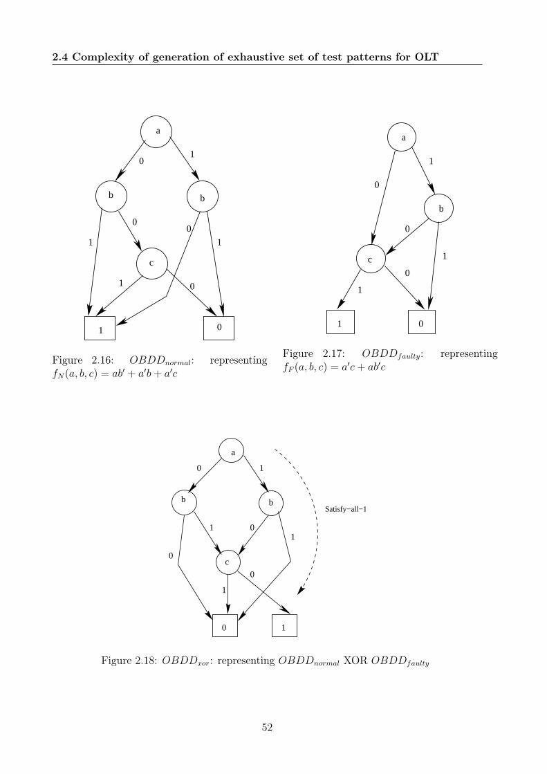
2.4 Complexity of generation of exhaustive set of test patterns for OLT
a
b b
c
1 0
01
00
1
1 0
1
Figure 2.16: OBDDnormal: representingfN(a, b, c) = ab′ + a′b+ a′c
a
b
c
01
1
0
0
0
1
1
Figure 2.17: OBDDfaulty: representingfF (a, b, c) = a′c+ ab′c
a
b b
c
0 1
0 1
1 0
0
1
0
1
Satisfy−all−1
Figure 2.18: OBDDxor: representing OBDDnormal XOR OBDDfaulty
52

2.5 Conclusion
• Feedback bridging fault: The simple XOR based procedure of generation of test
patterns using OBDDs may not be a direct approach for feedback bridging faults
because in some cases they create oscillations.
• Scalability: In case of OLT scheme at higher description level like behavioral level,
register transfer level, etc., the procedure of generation of test patterns using OBDDs
cannot be applied because OBDDs model the circuits at the gate level.
• OLT for asynchronous circuits: OBDDs have not yet been applied for OLT
of asynchronous circuits. So a study is required to find whether the XOR-OBDD
procedure is applicable to OLT of asynchronous circuits.
2.5 Conclusion
In this chapter we have discussed different types of OLT techniques for digital VLSI circuits
along with their pros and cons. It is seen that partial replication technique is widely used
compared to other techniques because of the advantages like non-intrusiveness, simplicity,
flexibility, etc. However, there are some shortfalls in this technique which are addressed in
the thesis; these are−(i) measurement limitation based flexibility, (ii) coverage for feedback
bridging faults, (iii) improvement in scalability and (iv) handling asynchronous circuits.
Also, different types of decision diagrams and their application in modeling and testing of
digital circuits have been discussed in this chapter. It is seen that OBDD is used in a straight
forward manner for generation of test patterns for OLT of circuits at gate level. However,
such a procedure of generation of test patterns using OBDDs cannot be directly applied to
the problems in case of measurement limitation, feedback bridging faults, circuits modeled
at higher level of abstractions and asynchronous circuits. So several extensions are required
to the XOR-OBDD procedure to address these problems.
In the next chapter we will address our first problem, i.e., designing a flexible OLT
scheme with the concept of measurement limitation using OBDD.
53


Chapter 3
On-line Testing with Measurement
Limitation
3.1 Introduction
On-line Testing (OLT) is performed when the circuit is in operational mode. It basically
involves continuous monitoring of the circuit and detecting the occurrence of a fault within
a finite time of its occurrence. Broadly speaking, there are four primary parameters that
are considered in design of an on-line tester−i) fault coverage, ii) fault detection latency, iii)
area overhead and iv) power overhead (Chapter 2, Subsection 2.1.4). The area and power
overheads of the on-line testers are high because they are designed using the exhaustive set
of test patterns for each fault of the circuit. If some faults and test patterns are dropped
then area and power overheads reduce, however, at the cost of fault coverage and detection
latency. Thus, one of the main requirements of OLT is to provide flexibility in the on-
line tester circuitry design. The OLT schemes reported in the literature [9, 12, 13] provide
flexibility in terms of trade-offs between area overhead of the tester versus fault coverage and
detection latency. These schemes have lowered the area overhead by considering a subset of
test patterns for design of the on-line tester circuit. However, the subset of test patterns is
selected in a fashion such that for all faults, at least one test pattern is present. Experimental
results in [9,12,13] have illustrated that very high fault coverage can be achieved even with
low area overheads. It is also shown that the impact of lowering the test patterns is almost
linear with the detection latency.
The on-line tester circuitry executes concurrently with the Circuit Under Test (CUT)
and needs to tap certain lines of the CUT. As the on-line tester is fabricated on the same chip
with the CUT, any point of the CUT can be easily tapped. This enables easy measurement
55

3.1 Introduction
of any required digital parameter of the CUT by the tester. So, most of the works on OLT
[9, 12, 13] (Chapter 2, Section 2.3) have ignored the issue of tap points or measurement
limitation. It may be noted that measurement limitation reduces load (fan-outs) on the
gates of the CUT which drive the tap points. This in turn reduces the number of additional
buffers required for driving the tester by the CUT, thereby decreasing the area overhead of
the tester. However, minimization of tap points also compromise fault coverage and detection
latency. This is because some of the test patterns generated for the full measurement case
no longer retain their capability to detect faults under measurement limitation. Therefore,
“number of tap points” can be used as a parameter to trade-off area overhead versus fault
coverage and detection latency.
In this chapter, we aim at developing a partial replication based OLT scheme for
digital circuits with measurement limitation. We also study the effect of minimizing tap
points on fault coverage, detection latency and area overhead, from the OLT perspective.
The scheme starts with generation of test patterns, called Fault Detecting transitions (FD-
transitions), for each fault of the circuit under full measurement. Following that, the FD-
transitions that remain so under a given measurement limitation are determined. Finally, on-
line tester, called Fault versus Normal condition detector (FN -detector), is designed using
these FD-transitions. The procedure of generation of FD-transitions and determination
of FD-transitions under measurement limitation are implemented using Ordered Binary
Decision Diagrams (OBDDs). Experimental results on ISCAS 89 benchmarks have been
presented, which illustrate that measurement limitation can be used as a trade-off parameter
to minimize area overhead to a great extent with minimal compromise in fault coverage and
detection latency. It is also found that for a given detection latency and coverage, area
overhead of the proposed scheme is lower compared to other similar schemes reported in the
literature.
This chapter is organized as follows. In Section 3.2 we discuss circuit modeling using
Finite State Automata (FSA) framework and FN -detector construction under measurement
limitation. Section 3.3 illustrates use of Ordered Binary Decision Diagrams (OBDDs) to
generate FD-transitions efficiently for construction of the FN -detector, which makes the
approach scalable. Section 3.4 presents experiential results regarding area overhead, fault
coverage and detection latency versus measurement limitation of the FN -detector. Finally
we conclude in Section 3.5.
56
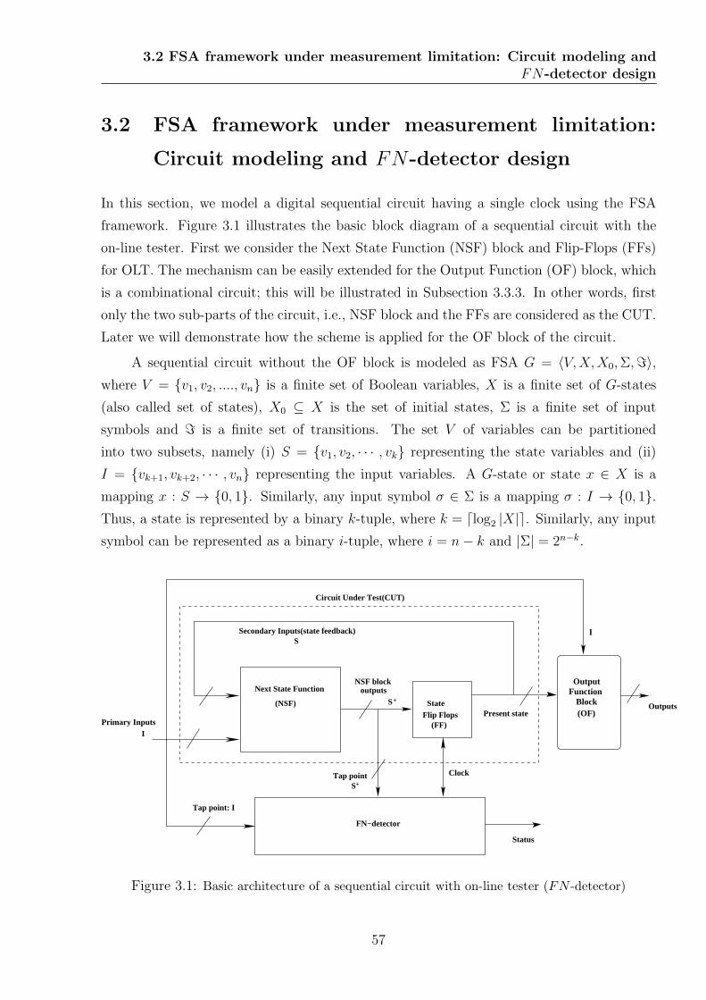
3.2 FSA framework under measurement limitation: Circuit modeling andFN-detector design
3.2 FSA framework under measurement limitation:
Circuit modeling and FN-detector design
In this section, we model a digital sequential circuit having a single clock using the FSA
framework. Figure 3.1 illustrates the basic block diagram of a sequential circuit with the
on-line tester. First we consider the Next State Function (NSF) block and Flip-Flops (FFs)
for OLT. The mechanism can be easily extended for the Output Function (OF) block, which
is a combinational circuit; this will be illustrated in Subsection 3.3.3. In other words, first
only the two sub-parts of the circuit, i.e., NSF block and the FFs are considered as the CUT.
Later we will demonstrate how the scheme is applied for the OF block of the circuit.
A sequential circuit without the OF block is modeled as FSA G = 〈V,X,X0,Σ,=〉,where V = {v1, v2, ...., vn} is a finite set of Boolean variables, X is a finite set of G-states
(also called set of states), X0 ⊆ X is the set of initial states, Σ is a finite set of input
symbols and = is a finite set of transitions. The set V of variables can be partitioned
into two subsets, namely (i) S = {v1, v2, · · · , vk} representing the state variables and (ii)
I = {vk+1, vk+2, · · · , vn} representing the input variables. A G-state or state x ∈ X is a
mapping x : S → {0, 1}. Similarly, any input symbol σ ∈ Σ is a mapping σ : I → {0, 1}.Thus, a state is represented by a binary k-tuple, where k = dlog2 |X|e. Similarly, any input
symbol can be represented as a binary i-tuple, where i = n− k and |Σ| = 2n−k.
Next State Function
(NSF)
Secondary Inputs(state feedback) S
NSF block outputs
S+ State Flip Flops
Tap point: I
I
Tap point S+
Clock
Status
FN−detector
Outputs
I
OutputFunction
Block(OF)
Circuit Under Test(CUT)
Primary InputsPresent state
(FF)
Figure 3.1: Basic architecture of a sequential circuit with on-line tester (FN -detector)
57

3.2 FSA framework under measurement limitation: Circuit modeling andFN-detector design
All input and state variables are not measurable. Let Im ⊂ I and Sm ⊂ S be the
subsets of measurable input and state variables, respectively. The unmeasurable state (input)
variables correspond to register-outputs (primary input lines) which are not tapped by the
on-line tester. The measurable input alphabet Σm = {σ|Im such that σ ∈ Σ} and the
measurable set of states Xm = {x|Sm such that x ∈ X} 1.
A transition τ ∈ = from a state x to another state x+ is an ordered three-tuple
τ = 〈x, σ, x+〉 where, x (initial(τ)) is the initial state of the transition, x+ (final(τ)) is
the final state of the transition and σ ∈ Σ (input(τ)) is the input symbol of the transition.
3.2.1 Circuit modeling under single stuck-at fault
Single stuck-at (s-a) faults are represented in the FSA model of a circuit using the following
steps:
• The variable set V is extended to include a subset C of l = dlog2(p + 1)e status
variables. Thus, V = S∪ I ∪C, where S and I are the sets of state and input variables
respectively, as given before, and p is the number of possible faults in the circuit.
• The state mappings are extended so that each becomes a mapping from S∪C to {0, 1}.⋃x∈X
x(C) = {N,F1, F2, · · · , Fp}, where N stands for normal status and Fi, 1 ≤ i ≤ p,
stands for the ith fault status. The image x(C) of C under x is called the fault label
of the state x.
The set of status variables are unmeasurable. The FSA model of a circuit (capturing
both normal and fault status) can be conveniently conceived as a collection of sub-machines,
one for the normal condition and one each for the faults F1, F2, · · · , Fp. The onset of a fault
Fi is captured by a transition from a state x1 with x1(C) = N to a state x2 with x2(C) = Fi;
such transitions are termed as si-transitions (for the start of fault Fi) and are represented as
si = 〈x1, T, x2〉, where x1(C) = N , x2(C) = Fi and “T” stands for “always true”. Due to the
occurrence of an si-transition, only the status variable changes its value from N to Fi and
all other state variables remain unchanged. Thus, si-transitions are unmeasurable. These
transitions need not occur at the triggering edges of the clock, i.e., they are asynchronous.
Their enabling conditions do not depend on any input variable combinations as they are
always true.
We use a flat indexing like x1, x2, · · · , xl when no differentiation needs to be made among
1x|Sm is the restriction of values x to set Sm. For example, if x = 〈v1v2v3〉 = 〈110〉 and Sm = {v1, v2},then x|Sm returns 〈11〉.
58

3.2 FSA framework under measurement limitation: Circuit modeling andFN-detector design
the sub-machines (normal or faulty). When we need to make a distinction between normal
and faulty sub-machines, the states for the normal sub-machine are designated as x0j, 1 ≤ j,
and those of the Fi-sub-machine are designated as xij, 1 ≤ j; likewise for the transitions.
Definition 3.1. N-state: A G-state is called normal (i.e., N -state), denoted as x0j, 1 ≤ j,
if x0j(C) = N . The set of all normal states is denoted as XN .
Definition 3.2. Fi-state: A G-state is called an Fi-state, denoted as xij, 1 ≤ j, if
xij(C) = Fi. The set of all Fi states is denoted as XFi.
Definition 3.3. Normal G-transition and Faulty G-transition: A G-transition
〈x, σ, x+〉 is called a Normal (Faulty Fi) G-transition if x, x+ ∈ XN(XFi).
Since faults are assumed to be permanent, there is no transition from any XFistate to
any XN state.
Definition 3.4. Measurement equivalent states: Two states x1 and x2 are measurement
equivalent, denoted as x1Ex2, if x1|Sm = x2|Sm.
Definition 3.5. Measurement equivalent transitions: Two transitions τ1 = 〈x1, σ1, x+1 〉
and τ2 = 〈x2, σ2, x+2 〉 are measurement equivalent, denoted as τ1Eτ2, if x1|Sm = x2|Sm,
x+1 |Sm = x+
2 |Sm and σ1|Im = σ2|Im.
In other words, two transitions are measurement equivalent if their source states are
measurement equivalent, destination states are measurement equivalent and so are the
inputs.
Throughout this chapter the simple example circuit given in Figure 3.2 is used to
illustrate the theory. A single s-a-1 fault F1 is assumed at the fanout branch marked A in
Figure 3.2. Figure 3.3 shows the FSA model for the circuit corresponding to the normal and
faulty behaviour.
3.2.2 FN-detector design for FSA model of a circuit
Let us first consider the circuit of Figure 3.2 under the case of full measurement i.e., Sm = S
and Im = I. If we compare the transitions under normal condition with the corresponding
ones after the s-a-1 fault in the FSA model given in Figure 3.3, it is seen that there is one
transition namely, 〈x11, 1, x13〉 : τ16, that implies a change in the circuit behaviour after
the fault. This is because, for transition 〈x11, 1, x13〉 : τ16 the corresponding transition in
normal condition is 〈x01, 1, x02〉 : τ06, where x01|Sm = x11|Sm = 10, σ06 = σ16 = 1 but
x02|Sm = 00 6= x13|Sm = 01. All other F1-transitions have an equivalent N -transition, e.g.,
59

3.2 FSA framework under measurement limitation: Circuit modeling andFN-detector design
v1+=v1v2+v2v3 v1
v2
D−FF
D−FF
v3
primary input
A
stuck−at−1
v1
v2
Clock
v2+=v1v2+v1’v2’
Figure 3.2: A simple sequential circuit with a s-a-1 fault
s1
s1
s1
x01
10
x02
00
x03
01
x11
10
x12
00
x13
01
FSA for normal circuitstatus variable:N
(s−a−1 at fanout branch marked A)FSA for circuit with fault
τ05:0
τ06:1
τ01:0
τ02:1τ03:0
τ04:1 τ15:0τ16:1
τ11:0τ12:1
τ13:0
τ14:1
<v1v2>
Trasition label
Transition enabling condition(value of input variable)
State label
values of state variables
status variable: F1
Figure 3.3: FSA model for the circuit of Figure 3.2
60

3.2 FSA framework under measurement limitation: Circuit modeling andFN-detector design
τ01Eτ11 ; so they cannot detect the fault. Hence, a Finite State Machine (FSM) can be
designed to determine if the following takes place. The CUT is in state x01 or in x11 (i.e.,
measured state variables are 10) and after that at input 1 the next state is x13 (i.e., the
measured state variables in the next clock period become 01); this indicates the s-a-1 fault.
We term this machine as an FN -detector (Fault versus Normal condition detector) and the
transition(s), that detect the faults, as FD-transitions (Fault Detecting transitions).
From the above observation, it appears that the FN -detector needs to monitor both
the NSF block outputs and the state flip-flop outputs. In case of the CUT of Figure 3.2, the
FN -detector may measure v1, v2 along with the NSF block outputs v+1 , v+2 and the input v3.
If the input vector 〈v1, v2, v3, v+1 , v+2 〉 = 〈10101〉, then the FN -detector can move to a fault
indicating state; else, on encountering 〈10100〉 (or any other don’t care pattern), it can loop
back to the same state.
Since the number of state variables in a typical VLSI circuit is quite high, the number of
inputs to the FN -detector circuit should be restricted. In this work, we are able to do so by
allowing the the FN -detector to monitor only the NSF outputs and detect an FD-transition
in two steps (in two consecutive clock cycles). The FN -detector, in the first clock cycle,
verifies whether the CUT is going to be in the initial state of the FD-transition. If it has
happened, then the detector, in the next clock cycle, examines if the primary input and the
NSF block output match, respectively, the input and the final state of the FD-transition.
Obviously, both these steps can be performed by measuring only the NSF block outputs.
It is to be observed that the technique still allows the FN -detector to move in step with
the CUT, i.e., both the FN -detector and the CUT can be driven by the same clock edge.
The basic schematic of the FN -detector vis-a-vis the CUT is shown in Figure 3.1. The
process of FN -detector construction from FD-transition is first demonstrated for the CUT
of Figure 3.2 and then we give a generalized treatment.
The state transition diagram of the FN -detector of the FSA model of the CUT,
shown in Figure 3.3, is given in Figure 3.4. This FN -detector detects the FD-transition
〈x11, 1, x13〉 : τ16. The detector starts from z0 (the initial state). State z1 is reached by the
transition t2 when the CUT traverses to the state x11 = inital(τ16), i.e., the measured NSF
block outputs v+1 and v+2 are 1 and 0, respectively. The value of the input variable v3 is a
don’t care (d) because the FN -detector depends only on the next state of the CUT to reach
z1. If the CUT moves to a state other than x11, (or x01), then t1, the self-loop transition,
takes place. So, the FN -detector reaches the state z1 simultaneously with the CUT moving
to the state x11 (or x01). The transition t3 from the state z1 represents the fact that the FD-
transition τ16 will occur in the CUT in the next clock edge because the NSF block outputs
61

3.2 FSA framework under measurement limitation: Circuit modeling andFN-detector design
z0
z1
zf
t2:<10d/0>
t4:<else/0>
t1:<else/0>
t3:<011/1>
t5:<all cases/1>
Initial state
Intermediate state
Final stateTransition label
output
Enabling condition
<output of NSF block− input variables>
<v1+ v2
+ v3>
FD−transition <x 11, 1, x13>
Figure 3.4: FN -detector for the FSA model of the circuit with a s-a-1 fault (Figure 3.3)
v+1 = 0 and v+2 = 1 and the input variable v3 = 1, as given by the 3-tuple 〈v+1 v+2 v3〉 = 〈011〉.Thus, the transition t3 leads the FN -detector to the final state zf yielding the output 1,
indicating that the s-a-1 fault has occurred at the fanout branch marked A. If such an
input-next state combination is not found in the state z1, then the FN -detector traverses
back to z0 by the transition t4. If the final state zf is reached, the detector always remains
in that state since the faults are permanent; the output is 1 indicating fault detection.
Now, we formally define the FD-transitions and the FN -detector.
Definition 3.6. FD-transition: An Fi-G-transition τik = 〈xik, σik, x+ik〉 is an FD-
transition, for fault Fi (denoted as FDi-transition), if there is a normal-G-transition
τ0l = 〈x0l, σ0l, x+0l〉 such that x0lExik, σ0l|Im = σik|Im and x+
0l 6E x+ik.
The set of all FDi-transitions is denoted as =FDi. The set of all FD-transitions for all
faults is denoted as =FD. Let =FDi= {τi1, τi2, · · · , τil}, where, 1 ≤ j ≤ l, τij = 〈xij, σij, x
+ij〉.
The FN -detector is driven by the same clock edge as the CUT. In general, there are
three types of states in any FN -detector − an initial state z0, a set of intermediate states
z1, z2, · · · , zl and a single final state zf . The initial state z0 keeps track of the next G-
state by monitoring the outputs of the NSF block v+1 , v+2 , · · · , v+k . The input variables
vk+1, vk+2, · · · , vn are don’t cares for the transitions emanating from z0. Whenever the CUT
is going to be in any state xij|Sm , for some τij ∈ =FDi, at the next clock edge, the FN -
detector moves to an intermediate state zk. Thus, there is a transition from z0 to zk (for
62

3.2 FSA framework under measurement limitation: Circuit modeling andFN-detector design
τij), labeled with the values of the measurable state variables corresponding to xij|Sm (i.e.,
initial(τij)); the outputs associated with all these transitions from z0 are 0. In the state
zk, the FN -detector keeps track of those outputs of the NSF block v+1 , v+2 , · · · , v+k which
are in Sm and inputs from vk+1, vk+2, · · · , vn which are in Im. If the input pattern matches
with σij|Im (i.e., input(τij)) and the NSF block output pattern matches with x+ij|Sm (i.e.,
final(τij)), then the FN -detector moves to the final state zf yielding an output 1; else it
moves back to z0. Thus, there is a transition from zk to zf (for τij), labeled with the values
of the measurable state variables corresponding to the state x+ij and the measurable values of
the input variables corresponding to σij. The set of FN -detector states, therefore, is given
by Z = {z0, z1, z2, · · · , zl, zf}, where z1, z2, · · · , zl correspond to the initial states of the FDi-
transitions. In a similar way FD-transitions of all other faults need to be incorporated in
the FN -detector by associating intermediate states with each transition. It is possible to
merge two intermediate states zk and zn into a single one if the corresponding FD-transitions
τij = 〈xij, σij, x+ij〉 and τln = 〈xln, σln, x
+ln〉 are such that xij|Sm = xln|Sm . Thus, the FN -
detector is a finite state machine given by the six-tuple,
GFN = 〈Z, z0,ΣZ , δZ , YZ , zf〉, (3.1)
where Z is the set of states, z0 is the initial state, ΣZ = Xm × Σm is the input alphabet,
δZ is the transition function, YZ is the output function and zf is the final state. Here,
δZ : Z × ΣZ → Z and YZ : Z × ΣZ → {0, 1}. The following steps are used for the
construction of the FN -detector.
1. Create an initial state z0 and final state zf .
2. For each FD-transition τij, repeat Step 3 and Step 4.
3. Create an intermediate state zk. Add a transition tk from z0 to zk. Input of tk is
v+1 , v+2 , · · · , v+k = initial(τij) co-joined with vk+1, vk+2, · · · , vn, which are don’t cares.
Output of tk is 0.
4. Add a transition tl from zk to zf . Input of tl is v+1 , v
+2 , · · · , v+k = final(τij) co-joined
with vk+1, vk+2, · · · , vn = input(τij). Output of tl is 1.
5. For each pair of intermediate states zk and zn, merge them into a single state, if the
corresponding FD-transitions τij = 〈xij, σij, x+ij〉 and τln = 〈xln, σln, x
+ln〉 are such that
xij|Sm = xln|Sm .
6. From each intermediate state zk, add a transition to z0. The enabling condition of
the transition is any value of v+1 , v+2 , · · · , v+k , vk+1, vk+2, · · · , vn other than the ones
63

3.2 FSA framework under measurement limitation: Circuit modeling andFN-detector design
corresponding to enabling conditions of transitions emanating from zk and leading to
zf . The output is 0.
7. Add a self loop in z0, whose enabling condition is any value of v+1 , v+2 , · · · , v+k , vk+1, vk+2,
· · · , vn other than the ones corresponding to enabling conditions of transitions
emanating from the initial state. The output is 0.
8. Add a self loop in zf , whose enabling condition is always TRUE (i.e., any value of
v+1 , v+2 , · · · , v+k , vk+1, vk+2, · · · , vn) and output is 1.
FN-detector under measurement limitation
Let us now examine the feasibility of an FN -detector under measurement limitation
Sm = {v2} and Im = {v3}, i.e., v1 is not tapped. In this case, the transition τ16 = 〈x11, 1, x13〉is an FD1-transition because there is a normal-G-transition namely, τ06 = 〈x01, 1, x02〉 suchthat x01|Sm = x11|Sm = 0, σ06|Im = σ16|Im = 1 and x02|Sm 6= x13|Sm because x02|Sm = 0 and
x13|Sm = 1.
Interestingly, however, τ16 cannot detect the fault F1 in an FN -detector as explained
below. Suppose we proceed to construct an FN -detector as follows. Since τ16 is measured
as 〈x11|Sm , v3|Im , x13|Sm〉 = 〈v2, v3, v+2 〉 = 〈0, 1, 1〉, on detecting v+2 to be 0, the FN -detector
would go to an intermediate state. Following that, if the input v3 is measured to be 1, and
v+2 is measured as 1, then the final state of the FN -detector is visited indicating fault F1.
However, the transition τ02 = 〈x02, 1, x03〉 will also be measured as 〈0, 1, 1〉; in other words, τ02
is measurement equivalent to τ16. Thus, under the measurement limitation being considered,
the FN -detector cannot detect the fault. So, we may say that τ16 no longer remains so under
measurement limitation Sm = {v2} and Im = {v3}. Let us now examine the feasibility of an
FN -detector under another measurement limitation Sm = {v1, v2} and Im = {}, i.e., inputv3 is not tapped. In this case, the transition τ16 = 〈x11, 1, x13〉 is an FD1-transition because
there is a normal-G-transition namely, τ06 = 〈x01, 1, x02〉 such that x01|Sm = x11|Sm = 10,
σ06|Im = σ16|Im = φ and x02|Sm 6= x13|Sm because x02|Sm = 00 and x13|Sm = 01. Interestingly,
unlike measurement restriction for v1, τ16 (measurement restriction for v3) can detect the fault
F1 in an FN -detector as explained below. Suppose we proceed to construct an FN -detector
as follows. Since τ16 is measured as 〈x11|Sm , v3|Im , x13|Sm〉 = 〈v1v2, φ, v+1 v+2 〉 = 〈10, φ, 01〉, ondetecting v+1 v
+2 to be 10, the FN -detector would go to an intermediate state. Following that,
if v+1 v+2 is measured as 01, then the final state of the FN -detector is visited indicating fault
F1. It may be noted that in the normal sub-machine (Figure 3.3) there is no transition which
is measured as 〈10, φ, 01〉, thereby successfully completing the FN -detector construction. So,
64

3.3 Efficient construction of FN-detector
in this case of measurement limitation, the FN -detector is capable of detecting the fault. In
other words, we may say that τ16 remains an FD1-transition under measurement limitation
Sm = {v1, v2} and Im = {}.Thus, it may be concluded that for some measurement limitation, certain FDi-
transition (under full measurement) becomes non-FDi-transition. Before we proceed to
the next section, we formally define FD-transition under measurement limitation Im and
Sm.
Definition 3.7. FDi-transition under Im and Sm: An Fi-G-transition τij = 〈xij, σij, x+ij〉
is an FDi-transition under Im and Sm, if there is a normal-G-transition τ0l = 〈x0l, σ0l, x+0l〉
such that x0lExij, σ0l|Im = σij|Im and x+0l 6E x+
ij. Further, there should not be any normal-G-
transition τ0m = 〈x0m, σ0m, x+0m〉 such that x0mExij, σ0m|Im = σij|Im and x+
0mEx+ij. The set
of all FDi-transitions for fault Fi under Im and Sm is denoted as =FDi|Im,Sm.
The inherent problem of constructing the FN -detector from the FSA model is that the
method becomes prohibitively complex even for simple VLSI circuits because the explicit
FSA model of a circuit is exponential in number of flip-flops in the circuit. In the next section,
we propose a scheme which is capable of detecting the FD-transitions (with measurement
limitation) directly from the circuit description without the need of the explicit FSA model
and, therefore, can be applied to fairly complex circuits.
3.3 Efficient construction of FN-detector
The NSF block is a combinational circuit with two types of inputs namely, the primary
inputs I and the secondary inputs S (which are feedback from the flip-flop outputs). The
NSF block outputs, denoted collectively as S+, determine the next state. This is illustrated
in Figure 3.5.
The NSF block can be described by the tuple S = 〈ΣS, S+〉, where ΣS = X × Σ is
the alphabet of input symbols (patterns) and S+ = {v+1 , v+2 , · · · , v+k } is the set of outputs
lines. For each v+i ∈ S+, 1 ≤ i ≤ k, v+i : ΣS → {0, 1}. Thus, an NSF output line
v+i also designates the switching function realized on this line. An input combination
σs ∈ ΣS is a mapping from V = {v1, v2, · · · , vk, · · · , vn} to {0, 1} represented as an n-tuple
〈σs(v1), σs(v2), · · · , σs(vk), σs(vk+1), · · · , σs(vn)〉, where the first k members constitute a k-
tuple of the secondary inputs and the remaining (n−k) members constitute an (n−k)-tuple
of the primary inputs.
Let S+i = {v+i1, v+i2, · · · , v+ik} denote the output maps represented by the NSF block
under fault Fi; similarly let S+0 = {v+01, v+02, · · · , v+0k} denote the output maps represented by
65

3.3 Efficient construction of FN-detector
Next state function
Primary inputs
Secondary inputs
IS+
(NSF)
NSF block outputs
Flip flops
(FF)
Clock
S
Figure 3.5: Input-output of the NSF block
the NSF block under normal condition. If we speak of the NSF block without the context of
faults (i.e., only in the normal condition), then S+ = {v+1 , v+2 , · · · , v+k } denotes its outputs.An FDi-transition τim = 〈xim, σim, x
+im〉 can be determined from the NSF block netlist
description in the following manner:
For the given s-a fault Fi, determine a value of the input combination of the NSF block
i.e., σs ∈ ΣS which sensitizes the fault and propagates the effect through the NSF block in
at least one of its outputs, i.e., ∃j, 1 ≤ j ≤ k, v+ij(σs) 6= v+0j(σs). As the secondary inputs
of the NSF block are the outputs of the state flip-flops, a secondary input pattern denotes
the current state from where there is an FD-transition. Hence, the first k-tuple of σs =
initial(τim) = xim. Similarly, the second (n − k)-sub-tuple of σs = input(τim) = σim. The
output of the NSF block (with fault Fi) corresponding to the input σs gives final(τim) = x+im
as 〈v+i1(σs), v+i2(σs), · · · , v+ik(σs)〉. To determine the set =FDi
, all possible values of σs are to
be determined such that ∃j, 1 ≤ j ≤ k, v+ij(σs) 6= v+0j(σs).
Now we study FD-transitions under measurement limitation. Given =FDi, subject to
measurement limitation Im and Sm, some of the FDi-transitions may not remain so. An in-
put combination σs ∈ ΣS under Im, Sm is represented as an n-tuple 〈σs(v1), σs(v2), · · · , σs(vk),
σs(vk+1), · · · , σs(vn)〉, where σs(vi) is d (don’t care), if vi /∈ Sm∪Im. For example, 〈d, σs(v2), · · · ,σs(vk), d, · · · , σs(vn)〉 represents the input combination when v1 /∈ Sm and vk+1 /∈ Im, i.e.,
NSF block output lines v+1 and v+k+1 are not measured. The input combination σs ∈ ΣS under
Im, Sm represents a set of input combinations (under full measurement) which are obtained
by replacing each d with 0 and 1. For example, if σs = 〈d, σs(v2), · · · , σs(vk), d, · · · , σs(vn)〉under v1 /∈ Sm and vk+1 /∈ Im, then σs|Im,Sm = {〈0, σs(v2), · · · , σs(vk), 0, · · · , σs(vn)〉,
66

3.3 Efficient construction of FN-detector
〈0, σs(v2), · · · , σs(vk), 1, · · · , σs(vn)〉, 〈1, σs(v2), · · · , σs(vk), 0, · · · , σs(vn)〉, 〈1, σs(v2), · · · ,σs(vk), 1, · · · , σs(vn)〉}.
An FDi-transition τim = 〈xim, σim, x+im〉 remains so under Im and Sm if
• Fault propagation is through a measured NSF output line: If σs (here xim × σim)
sensitizes the fault and propagates the effect through the NSF block in at least one of
its measured outputs, i.e., ∃j, 1 ≤ j ≤ k, v+ij(σs) 6= v+0j(σs) ∧ vj ∈ Sm.
• Under measurement limitation τim does not become equivalent to any N -transition: 6 ∃N -transition τ0l = 〈x0l, σ0l, x
+0l〉, such that ∃(x0l × σ0l) ∈ σs|Im,Sm and v+0j(x0l × σ0l) =
v+ij(σs),∀vj ∈ Sm.
For example, τ16 = 〈x11, 1, x13〉 (Figure 3.2) is an FD-transition. Here, x11 = 10, σ16 =
1, x13 = 01. Also, input combination is σs ≡ 〈σs(v1), σs(v2), σs(v3)〉 = x11×1 = 101. If Sm =
{v1, v2} and Im = {}, then input combination set σs|Im,Sm ≡ 101|v3 is 10d = {100, 101}. Here,v+01(100) = v+11(101) = 0 but v+02(100) = 0 6= v+12(101) = 1. Similarly, v+01(101) = v+11(101) = 0
but v+02(101) = 0 6= v+12(101) = 1. So τ16 = 〈x11, 1, x13〉 remains a FD1-transition even under
Sm = {v1, v2} and Im = {}. Now let us consider measurement limitation Sm = {v2}and Im = {v3}; input combination set σs|Im,Sm ≡ 101|v1 is d01 = {001, 101}. Here,
v+01(001) = v+11(101) = 0 and v+02(001) = v+12(101) = 1. So τ16 = 〈x11, 1, x13〉 does not
remain an FD1-transition under Sm = {v2} and Im = {v3}. The same conclusion was
arrived at in Subsection 3.2.2
Given a netlist description of the NSF block of the circuit, the set of FD-transitions
under Im and Sm can be determined in the following manner:
1. Simulate the NSF block under normal condition to determine output responses for all
input combinations.
2. Insert the s-a fault at the proper point in the NSF.
3. Simulate the NSF block with the fault for all possible input combinations.
4. Determine all possible values of inputs such that the output is different under fault
and normal condition; the corresponding transitions are FD-transitions under full
measurement (also called test patterns in off-line test terminology [17]).
5. For each FD-transition check if it remains so, under Im and Sm.
6. Repeat Steps (1) to (5) for all possible s-a faults.
67

3.3 Efficient construction of FN-detector
Step (1) through Step (4) basically involve determining all possible values of input
combinations for the NSF block that sensitize the fault and propagate its effect through at
least one NSF block output; this is called exhaustive test pattern generation [17]. Exhaustive
test pattern generation is a computationally hard problem. Further, to determine whether a
test pattern under full measurement remains so, even under a given measurement limitation
requires O(2k), where k = n − (|Sm| + |Im|), times analysis of the normal circuit. In other
words, a test pattern under full measurement represents a set of patterns under measurement
limitation, which are obtained by replacing each unmeasurable input by 0 and 1 (O(2k) in
number). So, like exhaustive test pattern generation procedure, this process of checking
test patterns under measurement limitation also involves exponential complexity. Hence, we
require optimized techniques for this problem.
The subsections that follow provide the details of these optimization steps. In essence,
these optimizations result by representing the NSF outputs as OBDDs [16] and devising
processing steps to work on these OBDD representations.
3.3.1 OBDD based procedure for exhaustive test pattern genera-
tion for the NSF block under full measurement
In this section we discuss the procedure for exhaustive test pattern generation for a fault Fi
for a given output line of the NSF block (under full measurement). Without compromising
fault detection capability, we assume that even if Fi is manifested at more than one NSF
output lines, any one of these lines can be used for its detection. Given an NSF block output
v+j and a fault Fi, two OBDDs are generated for the Boolean functions v+0j and v+ij , the
former for the normal condition and the latter under Fi. The two OBDDs are XORed and
the exhaustive set of input test vectors for Fi (that is, the exhaustive set of test patterns)
is the result of “satisfy-all-1” operation on the resulting XORed OBDD because all paths
leading to 1 in the XORed OBDD represent the exhaustive set of input patterns for which the
output under normal condition is different from that under the fault. The output response
v+ij , 1 ≤ j ≤ k, for the fault Fi, for the given set of input test vectors, can be easily obtained
form the OBDD for v+ij by applying the test patterns; this process can go hand in hand as the
test patterns are generated. Let us now illustrate this procedure for the s-a-1 fault, termed
as F1, at the fanout net marked A in the circuit shown in Figure 3.2. In this example, we
illustrate the OBDD with the ordering v1 ≺ v2 ≺ v3. Figure 3.6 represents the OBDD for the
Boolean function v+02 = v1v2+v′1v′2. Figure 3.7 represents the OBDD for the Boolean function
of v+12 = v1v2v′3 + v1v3 + v′1v
′2. Figure 3.8 represents the OBDD corresponding to v+02 ⊕ v+12
obtained by XORing the normal OBDD and the F1-OBDD illustrated in Figures 3.6 and 3.7,
68

3.3 Efficient construction of FN-detector
respectively. The exhaustive set of input patterns to test the fault F1 is obtained using the
satisfy-all-1 operation on the XORed OBDD (Figure 3.8) as {〈v1 = 1, v2 = 0, v3 = 1〉}, whichcorresponds to the single path from the root node (v1) of the XORed OBDD to the leaf node
1. The output response under fault (F1) for this input test pattern can be easily determined
using the F1-OBDD shown in Figure 3.7 as v+12 = 1. Thus, for the given fault F1 and the
NSF block output v+2 , the exhaustive test pattern set corresponding to the tuple 〈v1v2v3〉is given by {〈101〉}. The output for {〈101〉} corresponding to the tuple 〈v+1 v+2 〉 is {〈d1〉}.Thus, the FD-transition set for fault F1 and the NSF block output v+2 is {〈10, 1, d1〉}.
1 0
1
0 0
1
1 0
v1
v2 v2
v02+=v1v2+v1’v2’
Figure 3.6: OBDD for the function v02+ (circuit shown in Figure 3.2)
FD-transitions determined by the procedure discussed in the last paragraph detects a
fault by monitoring its manifestation at one NSF block output. However, it may happen that
for a given test pattern, Fi is manifested at one output line (say v+1 ) of the NSF block and for
another test pattern, Fi is manifested at some other output line (say v+2 ). While generating
the exhaustive FD-transitions for the output v+1 , we ignore the FD-transitions which may
lead to manifestation of F1 through v+2 . Ignoring these FD-transitions corresponding to v+2
may lead to rise in detection latency because they may include some input combinations
which are not covered in the FD-transitions for v+1 . To address this problem, therefore, the
exhaustive FD-transition sets are generated for each NSF output and for each Fi, which are
then used for designing an FN -detector for the entire NSF block. Let τ jim = 〈xjim, σ
jim, x
+jim〉
denote the mth FD-transition for the fault Fi determined at the NSF block output v+j . The
values of state variables in xjim are don’t care values for members of S+ whose corresponding
69

3.3 Efficient construction of FN-detector
v1
v2 v2
v3
1 0
1 0
0 0
1
1 0
1
v12+=v1v2v3’+v1v3+v1’v2’
Figure 3.7: OBDD for the function v12+ (circuit shown in Figure 3.2)
v1
v2
v3
1 0
satisfy−all−1
Normal OBDD XOR OBDD under F
1
1
1
0
0
0
1
Figure 3.8: XOR of v02+ and v12
+ OBDD (circuit shown in Figure 3.2)
70

3.3 Efficient construction of FN-detector
members in S do not fall under the cone of influence 2 of the NSF block output (v+j ) being
considered. Further, as the values of the variables corresponding to xjim conjoined with σj
im
are determined using OBDD (based XOR operation), even some of these variables that fall
in the cone of influence of v+j may be don’t cares. Also, it may be noted that only one
variable in x+jim, namely, v+j , that corresponds to the NSF block output through which the
fault manifestation is monitored has a Boolean value of 0 or 1; rest are don’t cares.
Once the exhaustive set of FD-transitions are generated for each fault, we check whether
the FD-transitions remain so under a given measurement limitation.
3.3.2 OBDD based procedure for determination of FD-transitions
under measurement limitation
Consider an FD-transition τ jim = 〈xjim, σ
jim, x
+jim〉 for the fault Fi determined at the NSF block
output v+j . Now we discuss the procedure to check if τ jim = 〈xjim, σ
jim, x
+jim〉 remains an FDi-
transition under measurement limitation Im and Sm, using OBDDs. Obviously, only those
NSF bock outputs are considered whose corresponding vj ∈ Sm (i.e., are measurable). In
other words, all FD-transitions where fault manifestation is only through NSF outputs which
are unmeasurable, can be directly dropped. So in this case, if vj is measurable (i.e., vj ∈ Sm)
then we proceed for further verification steps. Following that, we determine the value of the
NSF output (v+j ) under failure condition for input σjsm = xj
im × σjim by tracing the path in
the OBDD (representing output function for v+ij) corresponding to values of the variables
in σjsm; let the value be valjim ∈ 0, 1. Now, for each input combination under measurement
limitation Im, Sm i.e., σs ∈ σjsm|Im,Sm , we need to determine the value of NSF output (v+j )
under normal condition for input σs by tracing the path in the OBDD (representing output
function for v+0j) corresponding to values of the variables in σs; let the value be valj0σs∈ 0, 1. If
valj0σs6= valjim, for all σs, then τ jim remains an FDi-transition under measurement limitation
Im and Sm. Alternatively, if valj0σs
= valjim for any input condition σs ∈ σjsm|Im,Sm , then for
that σs, the corresponding NSF output v+j gives same value both in normal and faulty case;
τ jim does not remain an FDi-transition under measurement limitation.
Now we will illustrate the concept with the failure s-a-1 in line A (of Figure 3.2, whose
FSA model is shown in Figure 3.3) for measurement limitation (i) Im = {} and Sm = {v1, v2}(ii) Im = {v3} and Sm = {v2}. The FD1-transition is τ 216 = 〈10, 1, d1〉, corresponding to
NSF output v2. Here, σ2s6 = 10 × 1. If we traverse the OBDD for v+12 (for the fault,
shown in Figure 3.7) for the input combination 101 we have val216 = 1. For Im = {} and
2In terms of VLSI testing the sub-circuit that is in the transitive fanins of an (NSF) output, v+j say, is
called the “sub-circuit in the cone of influence of v+j ” [17]
71

3.3 Efficient construction of FN-detector
Sm = {v1, v2}, σs ∈ σ2s6|Im,Sm = {100, 101}. From the OBDD for v+02 (for the normal circuit,
shown in Figure 3.6), we have val20σs= 0 for both the input combinations of σs = 100 and
101, which is not equal to val216 = 1. So 〈10, 1, d1〉 remains an FD1-transition.
For Im = {v3} and Sm = {v2}, σs ∈ σ216|Im,Sm = {001, 101}. From the OBDD for v+02, we
have val20σs= 1 for combination σs = 001 which is equal to val216 = 1. So 〈10, 1, d1〉 does not
remain an FD1-transition.
Note: The above procedure to check if τ jim remains an FD-transition under measure-
ment limitation Im, Sm requires exponential number (with respect to unmeasurable lines)
of checks in the normal OBDD. However, using OBDD we can perform this step efficiently
as discussed below. In the OBDD representing the NSF output corresponding to v+j , under
normal condition, the following steps are required.
1. If vk ∈ Sm ∪ Im and σjsm(vk) = 0 (or 1) then in the node of the OBDD corresponding
to vk, eliminate the edge corresponding to 1 (or 0).
2. Delete all edges and nodes unreachable from the root after elimination of the edge.
3. Repeat Step 1 and Step 2 for all vk ∈ Sm ∪ Im.
4. In the resultant OBDD if there is a path from root to leaf whose value is same as that of
the corresponding faulty OBDD for input combination σjsm, then τ jim does not remain
an FDi-transition under measurement limitation; else it remains an FDi-transition.
In simple words, given an FDi-transition, we first replace all the variables of the input
combination with d which are unmeasurable. Now, in the normal OBDD, given a variable of
the input combination, we determine the corresponding nodes and keep the edge representing
0 or the edge representing 1 or both the edges, if the value of the variable is 0 or 1 or d,
respectively. This process is repeated for all variables of the input combination. In the
resultant OBDD, if there is a path to a leaf node whose value is same as that of the faulty
OBDD for the input combination of the given FDi-transition, then it does not remain an
FDi-transition under the given measurement limitation.
Let us consider the same s-a-1 fault (of Figure 3.2, whose FSA model is shown in
Figure 3.3) for measurement limitation Im = {v3} and Sm = {v2}. The FD1-transition in this
case is τ 216 = 〈10, 1, d1〉 corresponding to the NSF output v2. As already discussed, val216 = 1.
In the normal OBDD (Figure 3.6), as v1 6∈ Sm we retain both the edges for the variable v1.
As v2 ∈ Sm and value in the FD-transition is 0, we eliminate the edges corresponding to 1 in
the nodes for v2. Finally, as v3 ∈ Im and value in the FD-transition is 1, we need to eliminate
the edges corresponding to 0 in the nodes for v3; however, this need not be done as the nodes
72

3.3 Efficient construction of FN-detector
for v3 are redundant and already eliminated by the OBDD construction. Figure 3.9 shows
the normal OBDD for v+02 after edges and nodes for FD-transition 〈10, 1, d1〉 are eliminated
for Im = {v3} and Sm = {v2}. It may be noted that there is path from the root node to leaf
node with value 1, which is same as in the faulty OBDD (Figure 3.7) for input combination
〈101〉. So 〈10, 1, d1〉 does not remain an FD1-transition. In a similar way, it can be shown
that τ 216 remains FD1-transition under measurement limitation Im = {}, Sm = {v1, v2}.The FN -detector comprising FD1-transition τ 216 = 〈10, 1, d1〉 under measurement limitation
Im = {} and Sm = {v1, v2} for NSF output v+2 is shown in Figure 3.10.
v1
v2v2
1 0
1 0
0 0
Figure 3.9: OBDD for v+02 after edges and nodes for FD-transition 〈10, 1, d1〉 being eliminated forIm = {v3} and Sm = {v2}
3.3.3 FN-detector design for Output Function block of the circuit
The above procedure of design of the FN -detector can be easily applied to the Output
Function (OF) block of the circuit shown in Figure 3.1. To elaborate, we represent each cone
of the OF block using separate OBDDs under normal and faulty conditions. The same OBDD
based operations (applied for NSF block) are performed to generate the FD-transitions
under full measurement and determine the FD-transitions that retain their capability under
a given measurement limitation. Finally, the FN -detector is designed using these FD-
transitions. Since the OF block is a combinational circuit, its FN -detector design is much
simpler than that of the NSF block. An FD-transition generated for the OF block consists
of a combination of input values and its faulty response, whereas an FD-transition for the
NSF block, as discussed in Subsection 3.2.2, consists of initial state values, input and final
(faulty) state values. So, the FSM of the FN -detector for the OF block involves only two
state−initial state (z0) and final state (zf ) and any transition from z0 to zf indicates the
73

3.3 Efficient construction of FN-detector
z0
z1
zf
t2:<10d/0>
t4:<else/0>
t1:<else/0>
t3:<d1d/1>
t5:<all cases/1>
Initial state
Intermediate state
Final stateTransition label
output
Enabling condition(measurement limitation)
<output of NSF block−input variables>
<v1+v2
+d>
Enabling condition
<output of NSF block−input variables>
<d v2+d>
and NSF output v 2+=<10,d,d1>
FD−transition <x 11, 1, x13 ={ } and S m={v 1, v2}m
2+)(measurement limitation + NSF output v
> under measurement limitation I
Figure 3.10: The FN -detector for FD-transition τ16 under Im = {}, Sm = {v1, v2} and NSFoutput v+2
occurrence of a fault in the OF block. It may be noted that the fault detection in the OF
block is performed in a single clock cycle, whereas it requires two consecutive clock cycles
for the NSF block of the circuit.
We demonstrate the design of the FN -detector for the OF block using a simple
combinational circuit and avoid the detail formalisms. Figure 3.11 shows an OF block
having inputs−a, b, c, d and e, and outputs−OP1 and OP2. First, we partition the OF block
into cones with respect to its outputs as shown in the figure. Let us consider a s-a-0 fault
at point B (of Figure 3.11). As the fault belongs to cone of OP2, so we can propagate the
effect of the fault only through OP2. Under full measurement the test patterns to detect
the fault are (〈a, b, c, d, e〉) 〈10110〉 and 〈01110〉. These patterns produce output OP2 as 1
(0) under normal (faulty) condition. Suppose line a is not tapped by the FN -detector, then
the test pattern 〈d0110〉 does not retain its capability to detect the fault. This is because
the test pattern 〈d0110〉 comprises patterns 〈00110〉 and 〈10110〉 and the pattern 〈00110〉cannot detect the s-a-0 fault at B; value of OP2 is same under normal and faulty conditions
(i.e, OP2 = 0). However, the test pattern 〈d1110〉 retains its capability to detect the fault
because it comprises patterns 〈01110〉 and 〈11110〉 and both can detect the s-a-0 fault at
point B; value of OP2 is 1 (0) under normal (faulty) condition. The FSM of the FN -detector
74

3.3 Efficient construction of FN-detector
to detect the s-a-0 fault at B under measurement limitation (line a is not tapped) is shown
in Figure 3.12.
s−a−0
a
b
c
d
e
Inputs
cone for OP1
cone for OP2
OP1
OP2
Out
puts
B
Figure 3.11: Example of OF block
z0zf
t2:<else/0>
t3:<all cases/1>
t1:<d1110,0/1>
<inputs,output>fault status
initial state final state
Figure 3.12: FN -detector for the OF block (Figure 3.11) where line a is not tapped
75

3.4 Experimental evaluation
3.4 Experimental evaluation
The techniques discussed in Section 3.2 and Section 3.3 are used to design a tool “ML-OLT”,
which generates an FN -detector (in Verilog RTL) given a digital sequential circuit (in netlist
format). It basically involves the following steps:
1. Extract the the part of the netlist that corresponds to the NSF block.
2. Eliminate the flip-flops and partition the netlist (into sub-circuits) according to cones of
influence corresponding to each of the flip-flops. The output of each of the sub-circuits
is the corresponding input to the flip-flop.
3. Repeat the following for all the sub-circuits generated in Step 2.
(a) Insert s-a faults in all possible locations.
(b) Repeat the following for all the faults
i. Generate OBDD for the sub-circuit under normal condition.
ii. Generate OBDD for the sub-circuit under the fault condition.
iii. XOR the two OBDDs. The variable values corresponding to the paths to
leaf node “1”, are the input combinations for the FD-transitions. The faulty
OBDD output for an input combination determines the final state of the
FD-transition.
iv. Determine all the FD-transitions which remain so under the given measure-
ment limitation and drop the remaining ones.
4. Generate the FSM of the FN -detector with the remaining FD-transitions and translate
the FSM to Verilog code [24].
5. Generate the FSM of the FN -detector for OF block under measurement limitation
and translate the FSM to Verilog code.
In this thesis, we have used CUDD (Colorado University Decision Diagram) package
for the manipulation of OBDDs in order to generate FD-transitions. The CUDD package
is considered as the best-manipulated BDD package and is freely available. The package
provides a large set of operations on BDDs, like performing boolean operations (AND, OR,
XOR, etc.) on BDDs, Satisfying all 1/0 operations on BDD, etc.
The Verilog code can be synthesized using any standard synthesis tool, design library
and user defined constraints. Following that area overhead of the FN -detector can be
76

3.4 Experimental evaluation
determined for a given measurement limitation. As already discussed, along with area
overhead, other important parameters for the FN -detector are detection latency and fault
coverage. In the next sub-section we discuss regarding these parameters and how trade-offs
can be exploited in the FN -detector design.
3.4.1 Trade-offs in FN-detector design: detection latency, fault
coverage, measurement limitation and area overhead
The performance of an FN -detector in terms of fault detection can be represented in terms
of−(i) fault coverage and (ii) detection latency. The former deals with coverage of all possible
faults conforming to the single s-a fault model. Detection latency implies the number
of times a fault is manifested at some output of the CUT due to occurrence of an FD-
transition, however, is not detected because that FD-transition is not considered in the
FN -detector due to measurement limitation. Detection latency may increase due to two
factors namely, i) some FD-transitions may be kept out of the purview of the FN -detector
or ii) measurement limitation, which in turn eliminates some FD-transitions. So, when all
the FD-transitions are used to design the FN -detector, any fault is detected immediately
after it results in the first measurable difference in the output (compared to the normal
condition); thus, the detection latency is zero. Clearly, if some of the FD-transitions are
dropped in the construction of the FN -detector, then the detection latency may increase.
This is because the FD-transitions that are not taken in the FN -detector may occur before
the FD-transitions that are taken.
In [12], the area overhead was reduced by eliminating some FD-transitions. In the
present work we will use measurement limitation as a trade-off factor to minimize area
overhead by compromising detection latency and fault coverage. In [12], for most of the
cases (i.e., for the FD-transition set selected for the FN -detector) all primary inputs and
output lines had to be measured. In the experimental results we will show that similar
detection latency, fault coverage and area overhead can be achieved by the proposed scheme
compared to [12], however, with reduction in the lines to be measured.
The CAD tool “ML-OLT” is used to generate OLT circuits for different ISCAS’89
benchmark circuits under various measurement limitations. First we illustrate results (as
graphs) for fault coverage, detection latency and area overhead of the circuit s1488 under
different combinations of measurement limitations. We have illustrated results where 1 or
2 lines are considered unmeasurable. The following measures were used to determine the
values of fault coverage, detection latency and area overhead for a tester given a measurement
limitation.
77

3.4 Experimental evaluation
• Fault Coverage (FC): We consider a fault to be covered if at least one FD-transition
of the fault remains in the FN -detector under measurement limitation. Fault coverage
= ((number of faults covered)/(number of faults in the circuit)) ×100 %.
• Detection Latency (DL): For a fault Fi (which is covered), let there be nFDi
number of FD-transitions under full measurement. After measurement limitation
let nmlFDi be the number of FD-transitions that remain. Detection latency is
(dnFDi/nmlFDie)− 1.
• Area Overhead (AO): Area Overhead=(Area of the FN -detector after synthe-
sis)/(Area of the CUT after synthesis).
Figure 3.13, Figure 3.14 and Figure 3.15 illustrate detection latency, area overhead and
fault coverage, respectively of s1488 versus different combinations of measurement limitations
of one and two input lines of the NSF. Under this case of one and two input lines being
unmeasured, s1488 has 105 combinations of unmeasurable lines. In the graph, points in the
x-axis represent the line(s) not being measured; for example, the first point V 0 represents
that input V 0 is not measured whereas V 0 V 1 represents that V 0 and V 1 are not measured.
To keep the markings of the x-axis legible we illustrate only 55 combinations. The following
points may be noted:
• Figure 3.13: Impact of not measuring different (single or double) input lines may
have different impact on detection latency. As already discussed, making line(s)
unmeasurable results in converting some FD-transitions to non-FD-transitions which
leads to rise in detection latency. Broadly speaking, the input lines whose transitive
fanouts have more fault sites (i.e., gates) have higher sensitivity to detection latency.
• Figure 3.14: Lower the detection latency, higher the area overhead. Higher detection
latency implies that unmeasurable lines resulted in converting more FD-transitions to
non-FD-transitions compared to a situation with lower detection latency. Generally,
speaking an FN -detector with less FD-transitions involve less states resulting in
lower area and vice-versa. Same detection latency (due to different combinations of
unmeasured lines) may also result in different area overheads. Detection latency implies
that some FD-transitions are not considered, however, it does not specify which FD-
transitions. As circuit area does not only depend on the number of minterms but also
on the specific minterms and don’t cares [61], same detection latency (same number of
FD-transitions) may also result in different area overheads.
78

3.4 Experimental evaluation
• Figure 3.15: All combinations have fairly good fault coverage. Good fault coverage
can be achieved because if at least one FD-transition for the fault is present in the
detector, the fault is covered.
Detection Latency vs. Measurement Limitation
012345678
v0 v1v10v1
1v1
2 v2 v3 v4 v5 v6 v7 v8 v9CLR
v0_C
LR
v1_C
LR
v1_v
0
v1_v
10
v1_v
11
v1_v
12
v1_v
2
v1_v
4
v1_v
5
v1_v
7
v1_v
8
v1_v
9
v10_
CLR
v10_
v0
v10_
v2
v10_
v4
v10_
v5
v10_
v7
v10_
v8
v10_
v9
v11_
CLR
v11_
v0
v11_
v10
v11_
v2
v11_
v4
v11_
v5
v11_
v7
v11_
v8
v11_
v9
v12_
CLR
v12_
v0
v12_
v10
v12_
v11
v12_
v2
v12_
v4
v12_
v5
Lines not tapped
Dete
ction L
ate
ncy
Figure 3.13: Detection latency for s1488 versus different combinations of measurement limitationsof one and two input lines of the NSF
Area Overhead versus Measurement Limitation
0
0.1
0.2
0.3
0.4
0.5
0.6
v0 v1v10v1
1v1
2 v2 v3 v4 v5 v6 v7 v8 v9CLR
v0_C
LR
v1_C
LR
v1_v
0
v1_v
10
v1_v
11
v1_v
12
v1_v
2
v1_v
4
v1_v
5
v1_v
7
v1_v
8
v1_v
9
v10_
CLR
v10_
v0
v10_
v2
v10_
v4
v10_
v5
v10_
v7
v10_
v8
v10_
v9
v11_
CLR
v11_
v0
v11_
v10
v11_
v2
v11_
v4
v11_
v5
v11_
v7
v11_
v8
v11_
v9
v12_
CLR
v12_
v0
v12_
v10
v12_
v11
v12_
v2
v12_
v4
v12_
v5
Lines not tapped
Are
a O
ve
rhe
ad
Figure 3.14: Area overhead for s1488 versus different combinations of measurement limitations ofone and two input lines of the NSF
For some other ISCAS’89 benchmarks, we report in Table 3.1 the worst (i.e., highest)
and best (lowest) values of area overheads for 1, 2 and 3 combinations of unmeasurable lines.
The detection latencies corresponding to those combinations (of measurement limitation)
are also reported. Following that, for each of these detection latencies we determine area
overhead for the on-line tester. The table also compares area overhead of the proposed
scheme with the ones reported in [12, 36] for similar detection latencies. It may be noted
that we have not explicitly reported fault coverage because in all cases reported in the table,
79

3.4 Experimental evaluation
Fault Coverage versus Measurement Limitation
9293949596979899
100101
v0 v1v10v1
1v1
2 v3 v4 v5 v6 v7 v8 v9CLR
v0_C
LR
v1_C
LR
v1_v
0
v1_v
10
v1_v
11
v1_v
12
v1_v
2
v1_v
4
v1_v
5
v1_v
7
v1_v
8
v1_v
9
v10_
CLR
v10_
v0
v10_
v2
v10_
v4
v10_
v5
v10_
v7
v10_
v8
v10_
v9
v11_
CLR
v11_
v0
v11_
v10
v11_
v2
v11_
v4
v11_
v5
v11_
v7
v11_
v8
v11_
v9
v12_
CLR
v12_
v0
v12_
v10
v12_
v11
v12_
v2
v12_
v4
v12_
v5
v12_
v7
Lines not tapped
Fa
ult C
ove
rag
e
Figure 3.15: Fault coverage for s1488 versus different combinations of measurement limitations ofone and two input lines of the NSF
high coverage could be achieved. We have mainly dealt with area overhead and detection
latency because they are the most sensitive parameters.
Columns 1-2 provide information about the circuit. Columns 3, 5 and 7 correspond to
the lowest (best) area overhead obtained among all combinations of 1, 2 and 3 unmeasured
lines, respectively. Columns 4, 6 and 8 correspond to the highest (worst) area overhead
obtained among all combinations of 1, 2 and 3 unmeasured lines, respectively. In Column 9,
we report the amount of CPU time taken to generate the exhaustive set of FD-transitions.
Corresponding to each circuit (i.e., row 4 to row 13) we have reported values regarding, i)
AO: Area overhead of the FN -detector for the corresponding combination of unmeasured
lines ii) DL: detection latency due to the particular combination of unmeasured lines and
iii) AO[]: Area overhead of the FN -detector designed using the scheme of [12,36] to achieve
the particular detection latency; given a detection latency these schemes eliminate FD-
transitions randomly such that the given latency is maintained. For example, row 4-column
4, represents the single input line in circuit s27 (NSF block), whose unmeasurability gives
the best area overhead. The first element “AO:2.41” states that best case area overhead
is 2.41 for the corresponding single line being unmeasured. The second element “DL:2”
states that for the corresponding single line being unmeasured we get detection latency as
2. The third element “AO[]:2.45” states that for detection latency 2, the area overhead of
the FN -detector designed using the scheme [12, 36] is 2.45. The following conclusions can
be derived.
• Trends are similar to the case of s1488.
• The ranges between best case area overhead and worst case area overhead are fairly
high. Different input lines have different impact on transforming FD-transitions to
80

3.4 Experimental evaluation
Table 3.1: Area Overhead (AO) for different combinations of measurement limitations, resultingDetection Latency (DL), AO comparison with [12,36] and CPU time to generate FD-transitions∗
Circuit description AO for different combinations of measurement limitations CPU
Time
(Secs.)
Circuit No. of FFs-
(Gates)
one line two lines three lines
Best case
AO
Worst case
AO
Best case
AO
Worst case
AO
Best case
AO
Worst case
AO
S27 3-(10) AO:2.41 AO:2.99 AO:2.34 AO:2.66 AO:2.11 AO:2.51
DL:2 DL:1 DL:4 DL:1 DL:9 DL:2 19
AO[]:2.45 AO[]:2.99 AO[]:2.39 AO[]:2.99 AO[]:2.19 AO[]:2.45
S298 14-(119) AO:0.86 AO:1.36 AO:0.63 AO:1.34 AO:0.42 AO:1.32
DL:2 DL:1 DL:4 DL:1 DL:8 DL:1 228
AO[]:1.01 AO[]:1.88 AO[]:0.78 AO[]:1.88 AO[]:0.62 AO[]:1.88
S386 6-(118) AO:0.86 AO:1.38 AO:0.62 AO:1.25 AO:0.51 AO:1.13
DL:2 DL:1 DL:4 DL:1 DL:7 DL:1 411
AO[]:1.11 AO[]:1.80 AO[]:0.85 AO[]:1.80 AO[]:0.70 AO[]:1.80
S510 6-(211) AO:0.79 AO:1.2 AO:0.70 AO:1.1 AO:0.60 AO:1.0
DL:2 DL:1 DL:3 DL:1 DL:6 DL:1 1027
AO[]:1.1 AO[]:1.75 AO[]:0.88 AO[]:1.75 AO[]:0.72 AO[]:1.75
S5378 179-(2779) AO:0.4 AO:0.98 AO:0.23 AO:0.98 AO:0.18 AO:0.97
DL:2 DL:1 DL:3 DL:1 DL:6 DL:1 74141
AO[]:0.44 AO[]:0.98 AO[]:0.31 AO[]:0.98 AO[]:0.25 AO[]:0.98
S9234 228-(5597) AO:0.35 AO:0.99 AO:0.21 AO:0.97 AO:0.15 AO:0.97
DL:2 DL:1 DL:3 DL:1 DL:6 DL:1 221529
AO[]:0.39 AO[]:0.99 AO[]:0.3 AO[]:0.99 AO[]:0.21 AO[]:0.99
S15850 597-(9772) AO:0.3 AO:0.99 AO:0.20 AO:0.99 AO:0.18 AO:0.98
DL:2 DL:1 DL:3 DL:1 DL:5 DL:1 481115
AO[]:0.36 AO[]:0.99 AO[]:0.29 AO[]:0.99 AO[]:0.25 AO[]:0.99
S35932 1728-(16065) AO:0.28 AO:0.95 AO:0.20 AO:0.94 AO:0.17 AO:0.93
DL:2 DL:1 DL:3 DL:1 DL:5 DL:1 1023461
AO[]:0.35 AO[]:0.98 AO[]:0.28 AO[]:0.97 AO[]:0.24 AO[]:0.97
S38417 1636-(22179) AO:0.27 AO:0.89 AO:0.17 AO:0.88 AO:0.16 AO:0.87
DL:2 DL:1 DL:3 DL:1 DL:5 DL:1 1253624
AO[]:0.33 AO[]:0.95 AO[]:0.27 AO[]:0.94 AO[]:0.23 AO[]:0.93
S38584 1452-(19253) AO:0.27 AO:0.90 AO:0.18 AO:0.88 AO:0.17 AO:0.87
DL:2 DL:1 DL:3 DL:1 DL:5 DL:1 1221015
AO[]:0.34 AO[]:0.95 AO[]:0.28 AO[]:0.94 AO[]:0.24 AO[]:0.94∗Executed in AMD Phenom IIX3 710 Processor with 4 GB RAM in Linux OS.
81

3.5 Conclusion
non FD-transitions. This range can be utilized as a design parameter to trade-off area
overhead versus detection latency.
• For a given detection latency area overhead for the proposed scheme is lower compared
to that of [12, 36]. The scheme of [12, 36] randomly eliminates FD-transitions while
the proposed scheme performs this elimination by not measuring some input lines.
Not measuring some input lines of the NSF implies that they are not tapped by the
FN -detector. This reduces the fanouts of those input lines, resulting in less buffering
(drivers) and hence lower area.
3.5 Conclusion
In this chapter we have proposed an OBDD based OLT scheme of digital circuits with
measurement limitation (i.e., minimization of tap points of the CUT). The scheme provides
flexibility in terms of area overhead of the tester versus fault coverage and detection latency
with measurement limitation. The scheme uses “minimization of tap points” as a new trade-
off parameter to reduce area overhead at the cost of fault coverage and detection latency.
Experimentally, it has been shown that the minimization of tap points do not have high
impact on fault coverage and detection latency but it reduces area overhead of the on-line
tester. It is also observed that for a given detection latency, area overhead of the scheme is
lower compared to other similar schemes reported in the literature.
The s-a fault model is widely used in testing (and also in OLT) for its simplicity,
however, this model cannot capture more a fraction of real defects in modern day VLSI
circuits. So, advanced fault models such as bridging faults, delay faults, etc., are introduced
in testing in order to capture a large number of real defects. In next chapter, we will
address another important issue of OLT, i.e., OLT for advanced fault models. We have
taken bridging fault as the advanced fault model where both non-feedback and feedback
versions are considered.
82

Chapter 4
On-line Testing for Feedback Bridging
Faults
4.1 Introduction
In majority of the works on OLT, single stuck-at (s-a) fault model is considered. However
in modern integration technology, single s-a fault model can capture only a small fraction of
real defects and as a remedy, advanced fault models such as bridging faults, transition faults,
delay faults, etc., are now being adopted [135]. In this chapter, we focus towards OLT of one
of the most important advanced fault model, i.e., bridging faults. The first work on OLT for
bridging fault is reported in [73], which is based on self-checking design where the outputs
are encoded with error detecting codes and presence of any bridging fault would result in a
non-coded word as output. Biswas et al. in [13] have proposed an OLT scheme for bridging
faults which is based on the partial replication technique, where they have illustrated that
area overhead for OLT of bridging faults is not higher compared to that of s-a faults. The
main drawback of these two schemes is that they have only considered non-feedback bridging
faults and ignored feedback bridging faults. It may be noted that in some cases feedback
bridging faults cause oscillations and detecting them on-line using logic testing is difficult.
However, not all feedback bridging faults create oscillations and even if some does, there are
test patterns for which the fault effect is manifested logically. Directly dropping all feedback
bridging faults lead to significant compromise in fault coverage. Das et al. attempted to test
feedback bridging faults on-line in cluster based FPGAs [32]. There are two main issues with
this approach namely, intrusiveness of the design and use of asynchronous elements (Muller-
C elements). It may be noted that design of asynchronous tester for OLT of synchronous
circuit is not desirable. The details about these OLT schemes for bridging faults can be
83

4.2 Circuit modeling and FN-detector design using FSA framework
found in Chapter 2, Subsection 2.3.2.
Based on the literature review, in this chapter we propose a partial replication based
OLT scheme for wired AND-OR bridging faults. The scheme first determines the bridging
faults which do not lead to oscillations i.e., all non-feedback and some feedback bridging
faults. Following that, exhaustive set of test patterns for these faults are generated. Also, it
is checked if there are patterns, even in case of oscillating feedback bridging faults, which can
detect these faults without oscillations. All these test patterns taken together are used to
design the on-line tester, called FN -detector (i.e., fault versus normal condition detector).
All major steps of the scheme namely, checking if a feedback bridging fault causes oscillations,
generating exhaustive test patterns for non-feedback bridging faults and determining test
patterns that do not lead to oscillations in feedback bridging faults, etc., are implemented
using Ordered Binary Decision Diagrams (OBDDs) [16]. Application of OBDD enables
the proposed scheme to handle fairly complex circuits. On-line testers have been designed
for ISCAS 89 benchmarks. Experimental results illustrate that consideration of feedback
bridging faults along with non-feedback ones improve fault coverage with a marginal increase
in area overhead compared to schemes only involving non-feedback faults.
The chapter is organized as follows. Finite State Automata (FSA) based modeling
of the Circuit Under Test (CUT) with bridging faults and FN -detector construction are
explained in Section 4.2. To handle the issue of complexity of FN -detector construction,
several optimization techniques namely, partitioning the CUT using cones of influence, use
of OBDDs to generate fault detecting transitions without explicit state modeling, etc., have
been applied and are discussed in Section 4.3. Section 4.4 presents experimental results
regarding fault coverage and area overhead. Finally we conclude in Section 4.5.
4.2 Circuit modeling and FN-detector design using
FSA framework
The modeling procedure of sequential circuits for bridging faults using FSA is same as the
modeling framework discussed in the previous chapter (Chapter 3, Section 3.2). However,
we reproduce the FSA framework in brief for readability.
The basic architecture of a sequential circuit with on-line tester is shown in Figure 3.1
(Chapter 3). A sequential circuit (i.e., the CUT) comprises three blocks namely, Next
State Function (NSF), Flip-Flops (FFs) and Output Function(OF). In this work we mainly
consider the NSF block and FFs for OLT. The mechanism can be easily extended for the OF
block as it is a combinational circuit and is illustrated in Chapter 3, Subsection 3.3.3 for s-a
84

4.2 Circuit modeling and FN-detector design using FSA framework
faults. The same philosophy is applied for bridging faults and we do not present explicitly
in this chapter. A sequential circuit without the OF block can be modeled as an FSA G,
defined below.
G = 〈V,X,X0,Σ,=〉 (4.1)
where V = {v1, v2, ...., vn} is the finite set of Boolean variables, X is the finite set of states,
X0 ⊆ X is the set of initial states, Σ is the finite set of input symbols and = is the finite set
of transitions. The set of variables V can be partitioned into two subsets–(i) state variables
S = {v1, v2, ......vk} and (ii) input variables I = {vk+1, vk+2, .....vn}. A state x ∈ X is a
mapping x : S −→ {0, 1}. Similarly, any input symbol σ ∈ Σ is a mapping σ : I → {0, 1}.Thus, a state is represented by a binary k-tuple, where k = dlog2 |X|e; the value of the tupleis called encoding of the state. Similarly, any input symbol can be represented as a binary
i-tuple, where i = n− k and |Σ| = 2n−k.
A transition τ = 〈x, σ, x+〉 ∈ = is an ordered three-tuple, where x is the initial state
of the transition, denoted as initial(τ), x+ is the final state of the transition, denoted as
final(τ) and σ ∈ Σ is the input symbol of the transition, referred as input(τ).
4.2.1 Circuit modeling under bridging faults
The present subsection explains how sequential circuits having bridging faults are modeled
as FSA. In most of the works on bridging faults, short is assumed between any two lines in
the CUT. Ideally speaking, a bridging fault may involve any number of lines of a circuit,
however, that would make the number of all possible faults exponentially high. So, in the
widely accepted bridging fault models only two lines are assumed to be involved [17]. As
per the fault model, the manifestation is in terms of logic AND and logic OR between the
two lines. This fault model is called wired AND-OR fault model. In the CUT, the fault is
represented once by adding an AND gate and then by adding an OR gate between the two
lines involved in the fault. Henceforth in this chapter, the term fault will be used to refer to
wired AND-OR bridging fault. Whenever, any other fault needs to be refereed to, it would
be explicitly mentioned.
Fault is modeled as a part of the same FSA which is used to model the CUT under
normal condition. To elaborate, the FSA is divided into sub-systems (i.e., a sub-set of
states and transitions) and each sub-system is used to represent the CUT under a fault or
normal condition. So, the variable set V is extended as V = S ∪ I ∪ C, where C is a set of
k(= dlog2(p+1)e) status variables (normal or fault), where p is the total number of possible
faults in the CUT.⋃
x∈Xx(C) = {N,F1, F2, · · · , Fp}, where N stands for normal status and
85
4.2 Circuit modeling and FN-detector design using FSA framework
Fi, 1 ≤ i ≤ p, stands for the ith fault status. The image x(C) of C under x is called the fault
label of the state x. The state mapping is modified as (S ∪ C) −→ {0, 1}. It may be noted
that status variables are dummy variables only used for modeling and are unmeasurable. It
may be noted that if status variables are measurable then failure detection problem is trivial.
The occurrence of a fault (on the fly) Fi is captured by a transition from a state x1 with
x1(C) = N (in normal sub-system) to a state x2 with x2(C) = Fi (in Fi sub-system). For a
fault Fi such a transition is called si-transition (i.e., start of fault Fi) and is represented as
si = 〈x1, T, x2〉, where x1(C) = N, x2(C) = Fi. Firing of an si-transition does not depend
on input variables, rather it is “T” implying “always true”. Due to occurrence of an si-
transition, only the status variable changes its value from N to Fi and all the other variables
remain unchanged. Thus, si-transitions are unmeasurable. In synchronous circuits the state
register changes only at the triggering edges of the clock depending upon the inputs. So,
even if faults occur on the fly (in the NSF block) their effects are not manifested before the
next active clock edge when the circuit moves to a state that is different from the normal
condition. 1
Now we repeat the definitions of some terminologies in brief which are related to the
FSA model G. The detailed about the definitions can be found in Chapter 3, Section 3.2.
Definition 4.1. N-state and Fi-state: A G-state is called normal (i.e., N-state), denoted
as x0j, j ≥ 1, if x0j(C) = N . The set of all normal states is denoted as XN .
A G-state is called an Fi-state, denoted as xil, l ≥ 1, if xil(C) = Fi. The set of all Fi states
is denoted as XFi.
Definition 4.2. Normal G-transition and Faulty G-transition: A G-transition
〈x, σ, x+〉 is called a Normal (Faulty Fi) G-transition if x, x+ ∈ XN(XFi).
Definition 4.3. Measurement equivalent states: Two states x1 and x2 are measurement
equivalent, denoted as x1Ex2, if x1|S = x2|S; x1|S denotes the projection (i.e., values) of the
state variables in S.
Definition 4.4. Measurement equivalence transitions: Two transitions τ1 = 〈x1, σ1, x+1 〉
and τ2 = 〈x2, σ2, x+2 〉 are measurement equivalent, denoted as τ1Eτ2, if x1|S = x2|S, x+
1 |S =
x+2 |S and σ1|I = σ2|I .
1For explanation of our proposed OLT scheme we consider faults only in the NSF block. A bridging fault
in the flip-flops can be represented using a bridging fault involving the input and output lines of the NSF
block. It may be noted from Figure 3.1 that outputs and (secondary) inputs of NSF block are input lines
and output lines respectively, of the flip-flops.
86

4.2 Circuit modeling and FN-detector design using FSA framework
D−FF
D−FF
v1
v2
Primaryinput
v3
v1
v2 v1+=v1’v2+v2’v3
v2+=v1’v2’+v2v3
Clock
e1
e2
Figure 4.1: A simple sequential circuit.
D−FF
D−FF
v1
v2
Primaryinput
v3
v1
v2
Clock
e1
e2
Bridging(e1,e2)
v1+=v1v2
’v3+v1’v2
v2+=v1
’+v2
e1
e2*
*
Figure 4.2: Sequential circuit with AND-bridging between lines e1 and e2.
87

4.2 Circuit modeling and FN-detector design using FSA framework
In this work, we have taken a simple sequential circuit, shown in Figure 4.1, for
illustration of the theory. We assume a wired AND-bridging fault (denoted as F1) between
lines e1 and e2, as shown in Figure 4.2. The lines marked e∗1 and e∗2 represent the values of
lines e1 and e2 under the fault. All possible values at e1e2 are 00, 01, 10, 11. Among all these
four possibilities, 00 and 11 do not lead to any difference in logic values at any net in the
circuit under fault condition compared to the normal condition. However, if e1e2 = 01 then
e∗1e∗1 = 00 and if e1e2 = 10 then e∗1e
∗1 = 00. So, the wired AND-bridging fault between two
lines e1 and e2 is active only when these lines have different logic values. When e1e2 = 01,
then fault is manifested through only line e∗2, because e1 = e∗1 = 0 (i.e., there is no change in
e∗1 compared to e1 under fault) however, e2 = 1 6= e∗2 = 0 (i.e., there is change in e∗1 compared
to e1 under fault). In a similar way, when e1e2 = 10, then fault is manifested through only
line e∗1. So, it can be stated that in wired AND-bridging fault the line which has the logic
value 0 (e.g., e2 when e1e2 = 10) is “dominating” over the line, called “dominated” (e.g., e1
when e1e2 = 10), which has the value 1. In other words, in wired AND-bridging fault the
logic value at the dominating line is 0 which overrides the value at the dominated line by
pulling it from 1 to 0. This implies that wired AND-bridging fault results in s-a-0 fault at
the dominated line when the dominating line has the value 0.
Thus, test patterns for detecting the wired AND-bridging fault between lines e1 and e2
involve the following steps:
• All input patterns which result in e1 = 0 (dominating) and detect s-a-0 fault at
e2 (dominated), by propagating the fault effect at an output. This is illustrated in
Figure 4.3(a).
• All input patterns which result in e2 = 0 (dominating) and detect s-a-0 fault at e1
(dominated), by propagating the fault effect at an output. See Figure 4.3(b).
Note: In this chapter we will limit our discussion only on wired AND-bridging fault.
The mechanism for AND-bridging fault can be directly applied for OR-bridging fault by
applying the duality principle. For example, in case of OR-bridging the dominating line has
a value of 1 and it pulls the dominated line from 0 to 1, i.e., a s-a-1 fault.
As shown in Figure 4.1, under normal condition the expressions for the NSF block
outputs are v+1 = v′1v2+v
′2v3 and v+2 = v
′1v
′2+v2v3. The presence of the bridging fault changes
the output expressions to v+1 = v1v′2v3+v
′1v2 and v+2 = v
′1+v2 (Figure 4.2). Figure 4.4 shows
the FSA model for the normal and faulty behavior of the circuit. In the circuit modeling,
states for the normal submachine will be designated as x0j, 1 ≤ j, and those of the ith fault
(i.e., Fi-submachine) are designated as xij, 1 ≤ j; likewise for the transitions. In this example
88
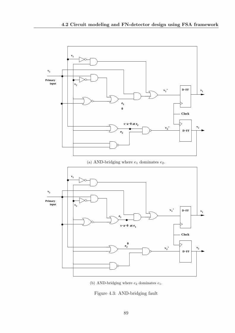
4.2 Circuit modeling and FN-detector design using FSA framework
D−FF
D−FF
v1
v2
Primaryinput
v3
v1
v2
Clock
e2
v1+
v2+
e1
s−a−0 at e2
0
(a) AND-bridging where e1 dominates e2.
D−FF
D−FF
v1
v2
Primaryinput
v3
v1
v2
Clock
e1
v1+
v2+e2
s−a−0 at e1
0
(b) AND-bridging where e2 dominates e1.
Figure 4.3: AND-bridging fault
89

4.2 Circuit modeling and FN-detector design using FSA framework
as there is a single fault denoted as F1, the faulty states and transitions are designated as x1j,
1 ≤ j and τ1j, 1 ≤ j, respectively. The occurrence of the fault is captured by the transitions
marked s1.
00
01
10
11
00
01
10
11
τ01:0
τ03:0 τ04:1
τ
τ
τ07:0τ02:1
τ08:1
τ11:0 τ :1
13:0τ
12
τ14:1
τ18:1
τ17:0
τ15:0
16:1
X01X11
X02 X12
X03X13
X04
X14
τ
<v 1,v2>
Transition
label
Transition
enabling condition(value of input variable)
valuesof state variables
State label
05:0
06:1
FSA for Normal Circuit
Status variable: N
FSA for Circuit with Bridging Fault
Status variable: F
s1
s1
s1
s1
1
Figure 4.4: FSA model for the circuit (of Figure 4.1) under normal and faulty condition
Now comparing the transitions under normal condition with the corresponding ones
after the bridging fault in the FSA model given in Figure 4.4, it is noted that there are
three transitions that reflect a change in behavior after bridging fault. These transitions
are τ12 : 〈x11, 1, x12〉, τ13 : 〈x12, 0, x14〉 and τ17 : 〈x14, 0, x12〉. This is because, for transition
τ12 : 〈x11, 1, x12〉 the corresponding transition in normal condition is τ02 : 〈x02, 1, x04〉, wherex01|S = x11|S = 00, σ02 = σ12 = 1 but x04|S(= 11) 6= x12|S(= 01). In simple words, in
these three transitions, for a given state and input variable combination the values of the
state variables in the next state are different in the normal model compared to its faulty
counter part. Such transitions that result in manifestation of faults are termed as FD-
transitions (i.e., Fault Detecting transitions). All other transitions in the normal model
have an equivalent counterpart in the faulty model; e.g., τ01Eτ11 because, τ01 : 〈x01, 0, x02〉,τ11 : 〈x11, 0, x12〉 and x01|S = x11|S = 00, σ01 = σ11 = 0, x02|S = x12|S = 01.
90

4.2 Circuit modeling and FN-detector design using FSA framework
D−FF
D−FF
v1
v2
Primaryinput
v3
v1
v2
Clock
e1
e2
v1+
v2+
1/01/0 1/0
(s−a−0 at e1)
=0
=0
=1
e2)(driving 0 to
0
1
0
1
1
Figure 4.5: FD-transition τ12 = 〈00, 1, 01〉 detects the given AND-bridging fault by driving 0 toline e2 and checking s-a-0 fault at line e1.
Now we show using the example of an FD-transition (τ12 = 〈00, 1, 01〉 say), that leadsto driving 0 at the dominating line and detects a s-a-0 fault at the dominated line. As shown
in Figure 4.5, τ12 = 〈00, 1, 01〉 implies that v1 = 0, v2 = 0, v3 = 1, which results in 0 at e2
and 1 at e1. Since we need to detect a s-a-0 fault at e1, applying 1 sensitizes the fault; this
is marked as “1/0” in e1 in Figure 4.5, which implies that under normal condition value of
the line is 1 and under the s-a-0 fault it becomes 0. It can be easily verified from the figure
that v1 = 0, v2 = 0, v3 = 1 also propagates the fault effect (i.e., 1/0) to the NSF output v+1 ,
leading to its detection. Similar can be shown for the other two FD-transitions.
4.2.2 FN-detector construction from the FSA model of the CUT
In this subsection we discuss the procedure to design an FN -detector using the FD-
transitions. The procedure is same as the one discussed in the previous chapter (Chapter 3,
Section 3.2, Subsection 3.2.2). We first refresh the definitions of the FD-transition and the
FN -detector, then discuss the design of FN -detector for the FD-transitions τ12, τ13 and τ17.
Definition 4.5. FD-transition: An Fi G-transition τij = 〈xij, σij, x+ij〉 is an FD-transition
for fault Fi, if there is a Normal G-transition τ0l = 〈x0l, σ0l, x+0l〉 such that x0lExij, σ0l = σij
and x+lj 6E x+
ij. Such an FD-transition is denoted as FDi-transition. The exhaustive set of
FDi-transitions is denoted as =FDi.
FN -detector is a Finite Sate Machine (FSM) having six-tuples, defined as
91

4.3 Efficient construction of FN-detector for bridging faults
GFN = 〈Z, z0,ΣZ , δZ , YZ , zf〉, (4.2)
where Z is the set of states, z0 is the initial state, ΣZ = X × Σ is the input alphabet,
δZ : Z×ΣZ → Z is the transition function, YZ : Z×ΣZ → {0, 1} is the output function and
zf is the final state.
Figure 4.6 represents the state transition diagram of the FN -detector for the FSA model
of the circuit under consideration. As discussed before the FD-transitions are τ12, τ13 and
τ17. In the detector, transitions t1, t2, t3, t4, t5 are responsible for checking if FD-transition
τ12 has occurred in the CUT. The detector starts from its initial state z0. Following that, if
the NSF block outputs 〈v+1 , v+2 〉 = 00 then the CUT is going to be in state x11 = initial(τ12)
(if fault has occurred) or x01 = initial(τ02) (if CUT is normal) in the next clock edge. The
detector reaches state z1 by the transition labeled t2 with the same clock edge. So the
detector reaches z1 along with the CUT reaching x11 or x01. It may be noted that enabling
condition of z1 is 00d, which implies that measured values of v+1 , v+2 = 00 and v3 is don’t
care (d). In simple words, for each FD-transition, in the FN -detector there is a transition
from the initial state to intermediate state with enabling condition as “NSF outputs equal to
values of state variables of the initial state of the FD-transition”. From state z1, the detector
needs to verify whether transition τ12 is going to occur in the CUT in the next clock edge.
The transition t3 from state z1 corresponds to this fact because enabling condition of t3 is
011, which implies NSF block outputs as v+1 = 0, v+2 = 1 and primary input as v3 = 1. Thus,
the transition t3 leads the FN -detector to the final state zf yielding output 1, indicating
that the bridging fault has occurred. If the enabling condition of t3 is not satisfied in state
z1 (i.e., v+1 = 1, v+2 = 1 and primary input as v3 = 1, corresponding to transition τ02), the
FN -detector moves back to the initial state by the transition t4. Once the final state zf is
reached, the FN -detector remains in that state forever maintaining the output as 1 since
the faults are assumed to be permanent.
In a similar way, the working of the detector for the other two FD-transitions τ13 and
τ17 can be explained; transitions t1, t6, t7, t8, t5 and t1, t9, t10, t11, t5 correspond to τ13 and τ17,
respectively.
4.3 Efficient construction of FN-detector for bridging
faults
While the procedure discussed in the last section can construct the FN -detector but its
complexity is prohibitively high. The reason is selection of the FD-transitions from the
92

4.3 Efficient construction of FN-detector for bridging faults
z 0
z 1
z 2
z 3
z f
<all cases/1>
t2
t t : <else/0>
<011 /1>t3:
t :5
t : <01d /0>
t7: <else/0>
t8: <110/1>
t9: <11d /0>
t10: <else/0>
t : <010/1>
Transition label
<outout of NSF block− input variable>
<v1+v +v3>
outputEnabling condition
Intermediate states
Final state
Initial state
1 <else/0>:
< 00d /0 >:
4
6
11
2
Figure 4.6: FN -detector for the FSA model of the circuit shown in Figure 4.4
FSA model in which the number of states can be exponential with respect to the number
of flip-flops in the CUT. In this section we propose an efficient scheme for construction
of FN -detector. The technique involves several optimization steps namely, partitioning the
CUT into smaller sub-parts based on cones of influence, determining FD-transitions without
explicitly constructing the FSA models using OBDD, etc., which have enabled design of on-
line testers for circuits having of the order of about ten thousand gates.
4.3.1 Partition of the CUT into sub-circuits using cones of
influence
From the basic architecture of a sequential circuit with on-line tester (shown in Chapter 3,
Figure 3.1), it may be noted that the NSF block of the CUT has two types of inputs;
primary inputs (I) and the secondary inputs (S). The secondary inputs are fed back from
the outputs of the flip-flops and represent the present state of the CUT. The outputs of
the NSF block are the next state of the CUT and denoted as S+. So, the NSF block
can be described as S = 〈ΣS, S+〉, where ΣS = X × Σ = v1, v2, · · · , vk, vk+1, · · · , vn is the
NSF input and S+ = {v+1 , v+2 , ..., v+k } is the NSF output. An input combination σs ∈ ΣS
is a mapping from V = {v1, v2, ...., vn} to {0, 1}, which can be represented as an n-tuple
〈σs(v1), σs(v2), · · · , σs(vk), σs(vk+1), · · · , σs(vn)〉, where the first k members correspond to
93
4.3 Efficient construction of FN-detector for bridging faults
secondary inputs (present state) and the remaining (n− k) members correspond to primary
inputs. For each v+j ∈ S+, 1 ≤ j ≤ k, v+j : ΣS −→ {0, 1}.Let S+
0 = {v+01, v+02, ..., v+0k} denote the NSF outputs under normal condition and
S+i = {v+i1, v+i2, ..., v+ik} denote the outputs under bridging fault Fi, 1 ≤ i ≤ p, where p is
the number of possible bridging faults. The jth FDi-transition τij = 〈xij, σij, x+ij〉 can be
determined from the NSF block directly, without explicit construction of the FSA model, in
the manner discussed below.
For a given bridging fault Fi, determine an input pattern of the NSF block, i.e., σs ∈ ΣS
which sensitizes the fault and propagates the effect through at least one of the NSF outputs,
i.e., if output of the faulty (Fi) NSF block for input σs is 〈v+i1(σs), v+i2(σs), · · · , v+ik(σs)〉, then
∃m, 1 ≤ m ≤ k, such that v+im(σs) 6= v+0m(σs). It may be noted that the first k-tuple of
σs = initial(τij) = xij. The second (n − k)-sub-tuple of σs = input(τij) and the output of
the NSF block (〈v+i1(σs), v+i2(σs), · · · , v+ik(σs)〉) gives final(τij) = x+
ij.
Given a netlist description of the NSF block of the CUT, the exhaustive set of FD-
transitions for the fault Fi (i.e., =FDi) can be generated as follows:
1. For all σs ∈ ΣS simulate the NSF block under normal condition to determine the
output response 〈v+01(σs), v+02(σs), · · · , v+0k(σs)〉.
2. Insert the bridging fault (Fi) at proper position in the NSF.
3. Simulate the NSF block with the fault Fi with each input σs to get the corresponding
output response 〈v+i1(σs), v+i2(σs), · · · , v+ik(σs)〉.
4. Select those σs such that ∃m, 1 ≤ m ≤ k, v+im(σs) 6= v+0m(σs). All such σs conjoined
with the outputs of the NSF block (for those σs), comprise the exhaustive set of FDi-
transitions.
5. Repeat Steps 2− 4 for all possible bridging faults.
The complexity of the above procedure for determining the exhaustive set of FD-
transitions is exponential with respect to the number of inputs of the NSF block (i.e., O(2n))
because |ΣS| = 2n. In case of reasonably complex VLSI circuits, n is of the order of thousands
and therefore there is a requirement of optimization techniques for exhaustive test pattern
generation. In this work, we address the issue using two techniques (i) divide the NSF
into sub-circuits using the principle of “cones of influence” with respect to the NSF output
lines. This technique divides the problem into sub-problems thereby lowering complexity;
(ii) OBDDs [16] have been used for all Boolean function operations required for test pattern
generation, checking if a pattern creates oscillation, etc.
94

4.3 Efficient construction of FN-detector for bridging faults
A combinational circuit can be represented as a Directed Acyclic Graph (DAG) where
a gate is represented by a node, the inputs to the gate are represented by directed edges into
the node and the gate outputs are represented by directed edges out from the node. The
nets in the circuit are represented by edges in the DAG. In this graph model, there are also
nodes representing primary inputs (called as source nodes) and primary outputs (called sink
nodes). The DAG representation of a circuit is defined as a tuple 〈N,E〉, where N is the set
of nodes and E is the set of edges. An edge e ∈ E is denoted by a tuple 〈n1, n2〉, n1, n2 ∈ N .
The node set is partitioned into three subsets–NSi: set of sink nodes (for primary outputs),
NSc: set of source nodes (for primary inputs) and NI : set of intermediate nodes (for gates).
There is no input edges into the source nodes and no output edges from the sink nodes.
A cone of influence of a net is a sub-circuit, which contains all the gates, nets and
inputs that are transitive fan-ins of the net (for which cone is being computed). Given a
DAG 〈N,E〉 of a combinational circuit, Algorithm 4.1 generates cones (i.e., sub-graphs of
〈N,E〉) corresponding to a net e1.
Algorithm 4.1 Algorithm for generation of cone of influence for a net e1.
Input: 〈N,E〉: DAG representation of the circuit
e1: Net for which cone is to be generated.
Output: gate cones(e1): set of gates in cone for e1
net cones(e1): set of nets in cone for e1
Create 〈N ′, E ′〉: Modified DAG of 〈N,E〉 where direction of all edges are reversed;
node cones(e1)← φ
edge cones(e1)← φ
Determine the node ne1 , such that 〈ne1 , n〉, where n ∈ N , is the edge corresponding to e1;
/* ne1 is the node from which the edge corresponding to net e1 emanates */
Perform Breadth First Search (BFS) in 〈N ′, E ′〉, where root node is ne1 ;
node cones(e1)← all gates corresponding to nodes visited in the BFS traversal;
edge cones(e1)← all nets corresponding to edges visited in the BFS traversal;
Using the above algorithm for each of the NSF outputs, it can be divided in cones.
Following that, OBBD based Boolean function manipulation techniques would be used to
generate the FD-transitions for the bridging faults. If the bridging fault is between two nets
from different cones then only those two cones need to be considered at a time for generating
the FD-transitions. However, in case of faults involving nets from a single cone, OBBDs
need to operate only on a single cone at a time. So, partitioning using cones of influence
limits the size of the CUT that needs to be handled at a time to a great extent.
95

4.3 Efficient construction of FN-detector for bridging faults
In the next two subsections we discuss in details the OBBD based scheme of generating
FD-transitions for non-feedback bridging faults and feedback bridging faults, respectively.
4.3.2 OBDD based procedure for generation of exhaustive set of
FD-transitions for non-feedback bridging faults
In this section we discuss the procedure for applying OBDD for generating the exhaustive
set of FD-transitions for a given non-feedback bridging fault Fi, between two lines e1 and
e2. As the fault is non-feedback, e1 does not lie in cone of influence of e2 and vice versa.
Initially, the normal circuit NSF is partitioned using cones of influence for each of the NSF
output lines. Let e1 be the dominated line and e2 be the dominating line. Fi is introduced
in the NSF block by inserting s-a-0 fault at the dominated line. Then the faulty NSF is
partitioned into cones for each of its outputs and those cones are selected which comprise
the dominated line. For each of these selected cones the following OBDD based operations
generate the set of FD-transitions for the fault.
1. Let the cone for v+m be one of the selected cones. Generate an OBDD for this cone.
This OBDD represents the Boolean function corresponding to v+m under s-a-0 fault at
the dominated line; let this OBDD be termed as “faulty OBDD”.
2. Consider the cone for NSF output v+m under normal condition (whose Boolean function
is v+0m) and represent it using an OBDD; it is termed as “normal OBDD”.
3. The two OBDDs (normal and faulty) are XORed and “satisfy-all-1” operation is
applied on the resulting XORed OBDD. The “satisfy-all-1” operation on an OBDD
generates all paths in terms of values of variables (of the Boolean function it represents)
that lead to leaf node with value 1. In the XORed OBDD, the paths leading to leaf node
with value 1 correspond to input patterns of the NSF cone under consideration, which
result in different values at NSF output v+m, under faulty (s-a-0 fault at dominated
line) condition compared to normal condition. Let IPs−a−0,dominated be the set of such
input patterns.
4. Generate a cone for dominating line in the NSF corresponding to the normal circuit.
Let the Boolean function corresponding to the dominating line be vdominating, which is
represented using another OBDD, termed as “dominating OBDD”.
5. The “satisfy-all-0” operation is applied on the dominating OBDD, which generates all
the input patterns for which the value at the dominating line is 0. The set of such
input patterns is IP0,dominating.
96

4.3 Efficient construction of FN-detector for bridging faults
6. The required test patterns that detect Fi (drives 0 to dominating line and detects
s-a-0 fault at dominated line) is obtained by the intersection of IPs−a−0,dominated and
IP0,dominating. These test patterns can be mapped to the initial state and input of the
FDi-transitions. The final state of the FDi-transitions can be obtained by applying
these patterns to the faulty OBDD, because the fault is manifested at the NSF output
v+m.
Note: Letτij = 〈xij, σij, xij〉 be the jth FDi-transition that detects fault Fi through
NSF output corresponding to v+m. τij can be obtained by mapping an input pattern (Step 3)
to initial(τij) conjoined with input(τij). The faulty output through the cone for v+m against
the pattern under consideration (Step 6) can be mapped to final(τij). The values of state
variables in initial(τij) and input variables in input(τij) are don’t cares which do not fall
under the cone of influence of v+m. Also, only one variable in final(τij) namely, v+im that
corresponds to the NSF block output through which the fault effect is monitored has a
Boolean value of 0 or 1; rest are don’t cares. We denote τmij = 〈xmij , σ
mij , x
+mij 〉 as the jth
FDi-transition which detects fault through cone corresponding to output v+m.
It may be noted that the procedure discussed above generates the exhaustive set of
FDi-transitions when e1 is the dominated line and e2 be the dominating line. This is only
half of the task, and it needs to be repeated by changing the roles of e1 and e2.
Now we explain the above procedure with the help of the circuit and the fault F1
shown in Figure 4.2. The partitioning of the NSF block (under normal condition) using
cones of influence on the NSF outputs is shown in Figure 4.7. First we assume that e1 is
the dominated line and e2 is the dominating line. The bridging fault under this case needs
inserting a s-a-0 fault at line e1 and enforcing 0 at e2. Following that, the faulty NSF is
divided into cones on its outputs; this is shown in Figure 4.8(a). It may be observed from
the figure that only cone for NSF output v+1 comprises e1. So OBDD based operations for
generating the FD-transitions are to be done only on the cone for v+1 .
The OBDD for cone of NSF output v+1 under normal condition (expression v′1v2+ v
′2v3)
is shown in Figure 4.9(a). Figure 4.9(b) illustrates the OBDD for NSF output v+1 under s-a-0
condition at e1 (expression v′1v2). The OBDD obtained after XORing the normal and faulty
OBDDs is shown in Figure 4.9(c). The “satisfy-all-1” operation on the XORed OBDD
generates the set IPs−a−0,dominated as {v1 = 1, v2 = 0, v3 = 1; v1 = 0, v2 = 0, v3 = 1}.Here, e2 is the dominating line and vdominating = v1 + v2, which is represented by the
dominating OBDD shown in Figure 4.9(d). “satisfy-all-0” operation on this OBDD generates
the set IP0,dominating as {v1 = 0, v2 = 0, v3 = d}, where d is don’t care, implying
IP0,dominating = {v1 = 0, v2 = 0, v3 = 0; v1 = 0, v2 = 0, v3 = 1}. The intersection of
97

4.3 Efficient construction of FN-detector for bridging faults
D−FF
D−FF
v1
v2
Primaryinput
v3
v1
v2 v +=v1’v2+v2’v3
v2+=v1’v2’+v2v3
Clock
e1
e2
NSFblock
cone 1
cone 2
1
Figure 4.7: NSF (normal condition) partitioned using cones of influence on its outputs.
IPs−a−0,dominated and IP0,dominating gives the set of test patters as {v1 = 0, v2 = 0, v3 = 1}.Signal values at the nets of the NSF block under s-a-0 fault at e1 for the test pattern
{v1 = 0, v2 = 0, v3 = 1} is shown in Figure 4.8(a). In the figure “1/0” implies that under
normal condition (s-a-0 fault at e1) the signal value at the corresponding net is 1(0). The
fault (s-a-0) manifestation at v+1 , when {v1 = 0, v2 = 0, v3 = 1} is obtained by applying the
pattern to the faulty OBDD, which comes to be 0. So the FD1-transition obtained from
the input pattern and fault manifestation is 〈00, 1, 0d〉, which corresponds to transition τ12
(Figure 4.4).
In a similar way, we determine the remaining FD1-transitions by reversing the roles of e1
and e2 (Figure 4.8(b)); the FD-transitions obtained are 〈01, 0, d1〉 and 〈11, 0, d1〉, whichcorrespond to τ13 and τ17, respectively.
4.3.3 OBDD based procedure for generation of exhaustive set of
FD-transitions for feedback bridging faults
As already discussed, the bridging between two lines is called feedback bridging if there exists
at least one path between these two lines. We refer the two lines involved in the feedback
98

4.3 Efficient construction of FN-detector for bridging faults
D−FF
D−FF
v1
v2
Primaryinput
v3
1
v2
Clock
e1
v1+
v2+
NSF block
v
e2
s−a−0 at e1
0
=0
=0
=1
1
0
1
1/01/0 1/0
0
(a) NSF with fault, partitioned into cones, when e2 dominates e1.
D−FF
D−FF
v1
v2
Primaryinput
v3
v1
v2
Clock
e2
v1+
v2+
s−a−0 at e
NSF block
e1
2
0
(b) NSF with fault, partitioned into cones, when e1 dominates e2.
Figure 4.8: NSF with faults (e2 dominates e1 and e1 dominates e2)
99

4.3 Efficient construction of FN-detector for bridging faults
0 1
01
1
00
1
01
v1
v2 v2
v3
(a) Normal OBDD for cone of NSF
output v+1 .
v1
v2
1 0
0
1
01
(b) Fault OBDD for cone of
NSF output v+1 (s-a-0 at e1).
v1
v2v2
v3
0 1
0 1
0 0
1
01
1
satisfy−all−1
(c) XORed OBDD for the normal and
faulty OBDDs.
v1
v2
0
10
1
01
satisfy−all−
0
(d) Dominating OBDD for line e2.
Figure 4.9: OBDDs for non-feedback bridging fault when e2 dominates e1
100
4.3 Efficient construction of FN-detector for bridging faults
bridging fault as the back line(b) and the front line(f), where b is closer to the primary
inputs and f is closer to the primary outputs. In other words, there is path from b to f .
The procedures of generation of test patterns for feedback bridging faults are discussed in
two parts. The first part discusses the procedure where f becomes the dominating line and
b becomes the dominated line and the second part deals with the reverse of that.
Part 1: Generation of exhaustive set of FD-transitions for feedback bridging
fault– the front line dominates the back line
The procedure for generation of the exhaustive set of FD-transitions for feedback bridging
faults (where f dominates b) involves all the steps required for the non-feedback bridging
faults (Subsection 4.3.2) namely, partitioning the normal NSF using cones of influence for
each of the outputs, introduction of fault by inserting s-a-0 fault at the dominated line,
partitioning the faulty NSF and finally generating the FD-transitions using OBDD based
operations.
However, additional steps are required in this case of feedback bridging fault to
determine if the FD-transitions cause oscillations. To elaborate, a test pattern that drives
0 to the dominating line (here f) and detects s-a-0 fault at the dominated line (here b) may
not qualify to become an FD-transition, if the fault effect at line b propagates through line
f and makes it 1. It is easy to observe that for sensitizing the fault, line f is driven to 0 and
effect of s-a-0 fault at line b is propagated to the NSF output, however, if the fault effect
makes f = 1, then there is oscillation.
The following steps based on OBDD are performed to check if the test patterns
generated using the scheme for non-feedback bridging faults (Subsection 4.3.2) cause
oscillations for the given feedback bridging fault where f dominates b.
Let TP be the set of test patterns obtained from the intersection of IPs−a−0,dominated
and IP0,dominating. TP is obtained using the steps discussed in Subsection 4.3.2, for the case
when e1, the dominated line is b and e2, the dominating line is f .
1. Generate a cone for the dominating line (i.e., f) in the faulty NSF (s-a-0 at b). Let
“dominating faulty OBDD” be the OBDD representation for the Boolean expression
corresponding to the dominating line f under the fault.
Apply the “satisfy-all-1” operation on the “dominating faulty OBDD”, which generates
all the input patterns for which the value at dominating line f becomes 1 under the
fault at dominated line b. The set of such input patterns be IPf=1,s−a−0 at dominated.
2. If there is a test patten tp in the intersection of TP and IPf=1,s−a−0 at dominated, then tp
101

4.3 Efficient construction of FN-detector for bridging faults
needs to be eliminated from the set TP . It may be noted that test pattern tp, implies
(i) 0 in the dominating line f under normal condition, (ii) different values in the NSF
output v+m under normal condition compared to s-a-0 fault at the dominated line b, (iii)
however, under fault, the dominating line f is pulled to 1. So, tp results in oscillation
under the fault.
The remaining set of test patterns in TP are mapped to FD-transitions.
A test pattern which remains in TP after the check implies (i) 0 in the dominating
line f under normal condition as well as faulty condition, (ii) different values in the
NSF output v+m under normal condition compared to s-a-0 fault at the dominated line
b. So such a test pattern can detect the fault without oscillation.
input(v3)
Primary
v1
v2
v1+
D−ff
D−ff
clock
b
v2+
NSFblock
(s−a−0) e1
e2
f1
0
0
0
1/0
0
1/0
1
0 0
1/0
1/0
feedback bridging fault(b,f) cone for line "f"
Figure 4.10: NSF with fault, partitioned into cones, when f dominates b.
Now we explain the above procedure with the help of a simple sequential circuit with
feedback bridging fault F1 between lines e1 and e2, as shown in Figure 4.10. Let e1 be the
dominated line (b) and e2 be the dominating line (f). The partitioning of the NSF into
cones on its outputs and on the dominating line are also shown in the figure.
The OBDDs for the cone of NSF output v+1 under normal condition (expression
v1v′2 + v
′1v2 + v
′1v3) and s-a-0 condition at e1 (expression v
′1v3 + v1v
′2v3) are shown in
Figure 4.11(a) and Figure 4.11(b), respectively. The OBDD obtained from XORing normal
102

4.3 Efficient construction of FN-detector for bridging faults
v1
v2v2
v3
1 0
0 1
0
1
10
01
(a) Normal OBDD for
cone of NSF output v+1 .
v1
v2
v3
0 1
1
0
0
1
0 1
(b) Faulty OBDD for
cone of NSF output
v+1 (s-a-0 at line b).
v1
v2 v2
v3
0 1
0 1
0
1 0
1
01
Satisfy_all_1
(c) XORed OBDD for the normal
and faulty OBDDs.
0
1
0
1
10
01
v1
v2
v3
Satisfy_all_0
(d) Dominating OBDD for the line f
under normal condition.
v1
v3
0
1
0
01
1
Satisfy_all_1
(e) Dominating faulty OBDD for
the line f (under s− a− 0 at b).
Figure 4.11: OBDDs for feedback bridging fault when f dominates b
103

4.3 Efficient construction of FN-detector for bridging faults
and faulty OBDDs is shown in Figure 4.11(c). The “satisfy-all-1” operation on XORed
OBDD generates the set IPs−a−0,dominated as {v1 = 1, v2 = 0, v3 = 0; v1 = 0, v2 = 1, v3 = 0}.Here, the dominating line is e2 (f) and vdomminating = v
′1v2 + v
′1v3, which is represented by
the dominating OBDD shown in Figure 4.11(d). The “satisfy-all-0” operation is applied on
this dominating OBDD which generates the set IP0,dominating = {v1 = 1, v2 = 0, v3 = 0; v1 =
1, v2 = 0, v3 = 1; v1 = 1, v2 = 1, v3 = 0; v1 = 1, v2 = 1, v3 = 1; v1 = 0, v2 = 0, v3 = 0}.The intersection of IPs−a−0,dominated and IP0,dominating gives the test pattern set TP as
{v1 = 1, v2 = 0, v3 = 0}.
Now, we check if the test pattern {v1 = 1, v2 = 0, v3 = 0} causes oscillation under
fault. The “dominating faulty OBDD” for the line e2(f) (expression is v1′v3) is shown
in Figure 4.11(e). Then “satisfy-all-1” operation is applied on this OBDD to generate
the set IPf=1,s−a−0 at dominated as {v1 = 0, v2 = 0, v3 = 1; v1 = 0, v2 = 1, v3 = 1}. Now
the intersection of TP and IPf=1,s−a−0 at dominated is φ, which implies that test pattern
{v1 = 1, v2 = 0, v3 = 0} can detect the feedback bridging fault F1, when f dominates b,
as it does not cause oscillation. The fault (s-a-0) manifestation at v+1 for the test pattern
{v1 = 1, v2 = 0, v3 = 0} is 0, thereby mapping to FD1-transition as 〈10, 0, 0d〉.
As discussed before, to generate the exhaustive set of FD1-transitions, now we need to
repeat this procedure when the roles of front line and back line are reversed i.e., generation
of exhaustive set of FD-transitions for feedback bridging fault, when back line dominates
the front line.
Part 2: Generation of exhaustive set of FD-transitions for feedback bridging
fault– the back line dominates the front line
In the circuit considered in Part 1 (Figure 4.10), if the roles of front line and back line are
reversed we obtain the circuit given in Figure 4.12. In this case, as back line (e1) dominates
the front line (e2), we drive 0 to the e1 and test for s-a-0 fault at e2. Using the OBDD
based operations to generate the test patterns (discussed in Subsection 4.3.2), we obtain TP
as {v1 = 0, v2 = 0, v3 = 1}. Now, it needs to be verified if the test pattern causes oscillation
under fault i.e., under fault, the dominating line b is pulled to 1. It may be noted that this
is not possible because fault effect cannot be propagated from the dominated line to the
dominating line. The reason is obvious, as there is no path from the dominated line to the
dominating line. So FD1-transition corresponding to this test pattern is 〈00, 1, 0d〉, as NSFoutput v+1 for this test pattern under fault is 0. So the exhaustive set of FD1-transitions is
{〈00, 1, 0d〉, 〈10, 0, 0d〉}.
104

4.3 Efficient construction of FN-detector for bridging faults
input(v3)
Primary
v1
v2
v1+
D−ff
D−ff
clock
v2+
NSFblock
(s−a−0)
f
cone for line "b"
1
0
0
e1b0 1
1
0
1
0
0
1
1/0
1/0
e2
feedback bridging fault(b,f)
Figure 4.12: NSF with fault, partitioned into cones when b dominates f .
Note: For any feedback bridging fault, all the test patterns generated for the case
“b dominates f” can be directly mapped to FD-transitions and used for FN -detector
construction (as they do not cause oscillation).
4.3.4 OBDD based procedure for illustration of an oscillating
feedback bridging fault
Now, we illustrate an example of a circuit where a feedback bridging fault (f dominates b,
case) causes oscillation.
The circuit in Figure 4.13 shows a feedback bridging fault F1 between lines e1 and e2.
As we are illustrating oscillation, e1 is the dominated line (b) and e2 is the dominating line
(f). The partitioning of the NFS into cones on its outputs and on the dominating line are
also shown in the figure. Using the OBDD based operations to generate the test patterns, we
obtain TP as {v1 = 1, v2 = 1, v3 = 0}. The expression for the line e2(f) under s-a-0 fault at
line e1(b) is v′1 + v′3. So, IPf=1,s−a−0 at dominated is {v1 = 0, v2 = 0, v3 = 0; v1 = 0, v2 = 0, v3 =
1; v1 = 0, v2 = 1, v3 = 0; v1 = 0, v2 = 1, v3 = 1; v1 = 1, v2 = 0, v3 = 0; v1 = 1, v2 = 1, v3 = 0}.As test pattern {v1 = 1, v2 = 1, v3 = 0} is included in the set IPf=1,s−a−0 at dominated, it
implies that the test pattern under fault would pull the dominating line (f) to 1, leading to
105
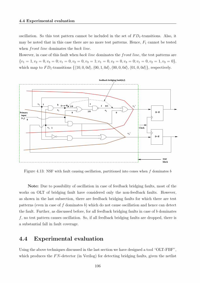
4.4 Experimental evaluation
oscillation. So this test pattern cannot be included in the set of FD1-transitions. Also, it
may be noted that in this case there are no more test patterns. Hence, F1 cannot be tested
when front line dominates the back line.
However, in case of this fault when back line dominates the front line, the test patterns are
{v1 = 1, v2 = 0, v3 = 0; v1 = 0, v2 = 0, v3 = 1; v1 = 0, v2 = 0, v3 = 0; v1 = 0, v2 = 1, v3 = 0},which map to FD1-transitions {〈10, 0, 0d〉, 〈00, 1, 0d〉, 〈00, 0, 0d〉, 〈01, 0, 0d〉}, respectively.
Primary input(v3)
v1
v2
D−ff
D−ff
Clock
v1+
v2+
NSFblock
b
e1 e2
1
1
0
(s−a−0) 1/0
0
1
1/0
f 0/1
0
feedback bridging fault(b,f)
Figure 4.13: NSF with fault causing oscillation, partitioned into cones when f dominates b
Note: Due to possibility of oscillation in case of feedback bridging faults, most of the
works on OLT of bridging fault have considered only the non-feedback faults. However,
as shown in the last subsection, there are feedback bridging faults for which there are test
patterns (even in case of f dominates b) which do not cause oscillation and hence can detect
the fault. Further, as discussed before, for all feedback bridging faults in case of b dominates
f , no test pattern causes oscillation. So, if all feedback bridging faults are dropped, there is
a substantial fall in fault coverage.
4.4 Experimental evaluation
Using the above techniques discussed in the last section we have designed a tool “OLT-FBF”,
which produces the FN -detector (in Verilog) for detecting bridging faults, given the netlist
106

4.4 Experimental evaluation
of a digital sequential circuit. On-line testers have been designed for several ISCAS’89 bench-
mark circuits using the tool OLT-FBF and performance in terms of fault coverage, detection
latency and area overhead have been analyzed.
Fault Coverage (FC): = Number of faults coveredTotal number of bridging faults in CUT
× 100%
Area Overhead (AO): = Area of the FN−detector (after synthesis)Area of the Circuit Under Test(CUT )
Detection Latency (DL): Detection latency for Fi is (dnFDi/nmlFDie)−1, where nFDi
is total number of FDi-transitions and nmlFDi be the number of FDi-transitions that are
considered in the FN -detector.
4.4.1 Fault coverage analysis
Table 4.1 shows the details of bridging fault coverage 2 achieved by the proposed scheme
for different ISCAS’89 benchmark circuits and comparison with [13]. Column 1 provides
information about the circuit i.e., circuit name (number of flip-flops, number of gates).
Column 2 shows the number of all possible AND-OR bridging faults. In Column 3, we report
the percentage of bridging faults which are non-feedback. The same column also represents
the fault coverage of the scheme proposed in [13]. It may be noted that the scheme reported
in [13] only handles non-feedback bridging faults. Percentage of non-oscillating feedback
bridging faults and oscillating feedback bridging faults 3 are reported in Column 4 and
Column 5, respectively. Column 6 represents the coverage of the proposed scheme i.e., sum
of non-feedback and non-oscillating feedback bridging faults. Strictly speaking, the proposed
scheme also covers the oscillating bridging faults partially, because even for such faults FD-
transitions are present in the FN -detector when b dominates f . In Column 7, we report the
CPU time taken to generate the exhaustive set of FD-transitions.
The following points may be noted:
• Broadly, about 10 to 20 percentage of bridging faults are feedback bridging faults.
However, among them only a small fraction (less than 1 percent) creates oscillations.
So neglecting all feedback bridging faults leads to substantial reduction in coverage,
which is the case in [13]. By filtering out the oscillating bridging faults and covering
the remaining bridging faults, i.e., non-feedback and non-oscillating feedback bridging
2detection latency was zero, i.e., all FD-transitions were considered in the FN -detector for the faults
covered3in this table a bridging fault is considered oscillating if there is a test pattern for which the circuit
oscillates, when the front line dominates the back line
107
4.4 Experimental evaluation
faults, more than 99 percentage of fault coverage is obtained for all the benchmark
circuits by the proposed OLT scheme.
• The number of feedback bridging faults is higher in circuits where the average number
of gates per cone of influence of the NSF outputs are large. The reason is explained as
follows. As we have seen, for a feedback bridging fault the back line should be within
the same cone as the front line. Obviously, larger cones imply more nets and more
such combinations of back lines and front lines.
It can be observed that the percentage of feedback bridging faults for the benchmark
circuit s382 having 21 flip-flops and 158 gates is 9.89 %. Whereas for the circuit s386,
having 6 flip-flops and 159-gates, the percentage is 15.17 %. It may be noted that these
two circuits have almost equal number of gates but only difference is in the number
of flip-flops. The average number of gates per cone in circuit s386 is 26.5, whereas in
case of s382 it is only 7.52. Similar trend can be seen for other circuits as well.
• The percentage of feedback bridging faults causing oscillations is low (less than 1
percent). In most of cases we have observed that a feedback bridging fault creates
oscillation if the back line involved in the fault has no other path for fault propagation
except through the front line; if back line belongs to more than one cones then
probability of this situation is low. It may be observed from Table 4.1 that in most of
the cases, higher the number of flip-flops (i.e., cones) in a circuit, lower is the number
of oscillating feedback bridging faults.
4.4.2 Area overhead analysis
If we design an FN -detector with highest possible fault coverage and target zero detection
latency (i.e., incorporate all FD-transitions for all faults in the FN -detector), area overhead
of the detector is high. So depending on the tolerable detection latency, some FD-transitions
may be dropped from each fault, thereby leading to reduction in area overhead.
Note: The scheme of blindly dropping FD-transitions based on given detection latency
is not applied for all faults. It has been observed that for some faults the number of FD-
transitions is quite less compared to others; such faults are called “difficult to test faults”.
If FD-transitions for such faults are dropped using the formula of detection latency (given
above), extremely low number or no FD-transition will be present in the FN -detector for
such faults. This would practically imply that the fault is dropped, leading to compromise
in fault coverage, which is not desirable. So, in this work, a threshold is determined based
on the input space of the CUT and all faults whose number of FD-transitions are less than
108

4.4 Experimental evaluation
Tab
le4.1:
Fau
ltcoverage
bytheproposed
method,comparisonwiththeexistingtechnique[13]andCPU
timeto
gen
erateFD-transition
s∗
ISCAS’89
bench
mark
Tota
l#BFs+
#Non-F
BFs(%)+
#FBF(%
)+#Oscillating-
FBFs(%)
Fault
covera
ge(%
)CPT
Tim
e
circuits-(F
Fs,GATEs)
Fault
covera
ge(%
)[13]
Pro
posed
scheme
(Secs.)
s298-(14
,119
)91
8090
.94
9.06
0.860
99.14
329
s344-(15
,160
)16
836
85.96
14.04
0.623
99.377
780
s382-(21
,15
8)16
471
90.11
9.89
0.631
99.369
720
s386-(6,15
9)14
706
84.83
15.17
0.904
99.096
522
s713-(19
,393
)99
681
76.73
23.27
0.985
99.015
3410
s838-(32
,446
)13
0816
91.15
8.85
0.623
99.377
3823
s1238-(18,50
8)14
5530
89.25
10.75
0.717
99.283
5012
s1423-(74,65
7)27
9378
83.07
16.93
0.608
99.392
11215
s5378-(179
,277
9)44
7752
879
.86
20.14
0.598
99.402
155730
s9234-(228
,559
7)17
0732
4678
.72
21.28
0.611
99.389
485982
s13207
-(66
9,79
51)
3741
5575
78.12
21.88
0.602
99.398
811764
s15850
-(59
7,97
72)
5389
8153
77.13
22.87
0.590
99.410
942365
s35932
-(17
28,160
65)
1589
0987
875
.28
24.72
0.537
99.463
2267521
s38417
-(16
36,221
79)
2842
3240
374
.14
25.86
0.522
99.478
2872524
s38584
-(14
52,192
53)
2145
8668
674
.27
25.73
0.525
99.475
2512320
+BFs:
bridgingfaults,
FBFs:
feedbackbridgingfaults,
Non-FBFs:
non-feedback
bridgingfaults.
∗ Executedin
AMD
Phenom
IIX371
0Processor
with4GB
RAM
inLinuxOS.
109

4.4 Experimental evaluation
the threshold are marked as difficult to test faults. All FD-transitions corresponding to
such faults are included in the FN -detector. This rarely leads to a significance rise in area
overhead because of the low number of extra transitions that are required to be explicitly
included in the FN -detector.
Table 4.2 shows the area overhead of the FN -detector for different ISCAS’89 benchmark
circuits under different values of detection latency.
The following points may be noted
• As expected, increase in detection latency results in reduction in area overhead of the
FN -detector.
• For a given detection latency, area overhead decreases with increase in size of the circuit
and finally saturates. For partial replication based OLT for s-a faults, Drineas et al.
in [35] identified the fact that area overhead ratio is approximately α + 1/k, where
α is the fraction of the test patterns incorporated in the tester design (i.e., detection
latency in our case) and k is the number of state bits (generally proportional to circuit
size). It can be observed from Table 4.2 that the dependence of area overhead ratio
with detection latency adheres (approximately) to the above-mentioned fact, even for
bridging faults. For example, in case of a small circuit (s298), where the number of
state bits is 14, area overhead is nearly three times even for detection latency of 9.
However, the area overhead for a large circuit (s9234), where state bits are 228, is less
than one fourth for the same latency. From the table it may be noted that this trend
follows for all the benchmark circuits considered.
Thus, for most of the practical circuits (which generally have more than tens of
thousands of gates), near hundred percent bridging fault coverage can be achieved
with reasonably low area overheads by suitably compromising detection latency.
• For a given latency, the proposed scheme leads to slightly higher area overhead
compared to [13]. The reason is, more FD-transitions in the detector due to the
additional coverage of feedback bridging faults in the proposed scheme compared to
[13].
• It can be seen in Table 4.2 that the area overheads for small sized circuits (i.e., from
s298 to s713) are more than 200% even for detection latency 9, where as for large
sized circuits it gradually decreases to around 10%. So it may be concluded that the
proposed scheme provides high fault coverage and tolerable latency at reasonable area
overhead for circuits having more than thousand gates (which is typically the case for
most of the practical circuits).
110

4.4 Experimental evaluation
Tab
le4.2:
Areaoverheadfortheproposedmethodandcomparisonwith[13]
ISCAS’89bench
mark
Are
aoverh
ead
forDetection
latency
circuits-(F
Fs,GATEs)
ForDetection
latency=0
ForDetection
latency=4
ForDetection
latency=9
[13]
Pro
posed
work
[13]
Pro
posed
work
[13]
Pro
posed
work
s298
-(14
,119
)2.85
3.03
2.80
2.86
2.64
2.72
s344
-(15
,160
)2.83
3.04
2.74
2.85
2.43
2.49
s382
-(21
,15
8)2.9
3.12
2.81
2.90
2.53
2.58
s386
-(6,15
9)2.88
3.28
2.78
2.94
2.48
2.61
s713
-(19
,393
)2.37
2.96
1.98
2.16
1.82
1.90
s838
-(32
,446
)1.5
1.64
1.38
1.52
1.21
1.32
s123
8-(18,50
8)1.48
1.54
1.18
1.31
1.13
1.22
s142
3-(74,65
7)1.44
1.51
1.10
1.21
1.05
1.11
s537
8-(179
,277
9)1.25
1.32
0.5
0.61
0.21
30.225
s923
4-(228
,559
7)1.23
1.29
0.44
0.57
0.20
90.219
s132
07-(66
9,79
51)
1.22
1.27
0.41
0.53
0.20
60.217
s158
50-(59
7,97
72)
1.18
1.22
0.33
0.45
0.17
80.190
s359
32-(17
28,160
65)
1.05
1.13
0.16
70.21
50.12
10.131
s384
17-(16
36,221
79)
1.02
1.11
0.15
90.19
20.11
30.123
s385
84-(14
52,192
53)
1.03
1.12
0.15
80.18
30.11
00.117
111

4.5 Conclusion
• Since the area overheads of all the above benchmark circuits are greater than 100% for
zero detection latency, it can be argued that simply duplicating the original circuit and
comparing the responses would be much simpler and effective technique. However, the
main drawback of this full duplication scheme is that, same type of fault may occur
in both the circuits (original and duplicate) and in such case fault detection is not
possible. Such faults are called common-mode failures and it has been identified by
Mitra et al. [75] that their number is reasonably high, which reduces the efficacy of
pure duplication based OLT.
4.5 Conclusion
In this chapter, we have proposed an OBDD based OLT scheme of digital circuits for AND-
OR bridging faults. Most of the reported works on OLT of bridging faults cover only
non-feedback bridging faults, whereas the proposed scheme covers both feedback and non-
feedback bridging faults. Experimentally, it has been shown that on an average 20% of all
possible bridging faults are feedback, however, only less than 1% of them cause oscillations.
So, significant improvement in fault coverage is achieved by considering both feedback and
non-feedback bridging faults. It is also observed that there is marginal increase in area
overhead of the proposed scheme compared to the techniques considering only non-feedback
bridging faults.
None of the OLT schemes including the OBDD based ones, could scale up to the level of
complexity incurred in modern day circuits which have tens of thousands of gates. The major
reason being most of these OLT schemes work at gate level, leading to the state explosion
problem. So, one of the most important issues of the gate level OLT schemes is scalability.
In the next chapter, we will address the issue of scalability by proposing an OLT scheme for
the circuits at Register Transfer Level (RTL). The scheme uses High Level Decision Diagram
(HLDD) instead of OBDD in OLT (for circuits at gate level).
112

Chapter 5
On-line Testing at Register Transfer
Level
5.1 Introduction
One of the important issues of OLT in modern deep sub-micron design is scalability. Most
of the OLT schemes reported in the literature including the ones proposed in Chapter 3
and Chapter 4 work at logic gate level and are scalable only up to a certain extent, i.e.,
circuits having about 30 thousand gates and 500 flip-flops. This is because these schemes
are designed at logic gate level leading to the state explosion problem. In order to solve this
issue, i.e., to improve the scalability, a number of OLT schemes at higher description level
have been proposed [43,57,58]. The details about these schemes can be found in Chapter 2,
Subsection 2.3.3. The OLT schemes at Register Transfer Level (RTL) presented in [43, 58]
are based on replicating each operation and executing them using different functional units
in the idle computational clock cycles. Outputs of these functional units are compared and
the faulty functional units are detected. The scheme discussed in [57] is based on exploiting
RTL implementation diversity to detect both transient and permanent faults on-line. The
technique applies allocation diversity by changing operation-to-operator allocation and data
diversity by shifting operands before re-computation. Faults can be detected by comparing
the results obtained from normal computation and re-computation. All of these OLT schemes
have a number of drawbacks−(i) they are intrusive in nature since they require some special
properties in the circuit structure, (ii) they have high latency because they depend on idle
times of different functional units of the CUT, (iii) they are architecture specific because of
the use of secondary functional units, etc.
Similar to the schemes discussed in Chapter 3 and Chapter 4, in this work we develop
113

5.2 High-Level Decision Diagram
a partial replication based OLT scheme at RTL in order to overcome the drawbacks of the
schemes reported in [43, 57, 58]. However, unlike the use of OBDD for gate level circuits
(in Chapter 3 and Chapter 4), this scheme uses High Level Decision Diagram (HLDD)
for circuits at RTL. The CUT is partitioned into a number of sub-circuits and each sub-
circuit is represented using different HLDDs under normal and faulty conditions. For each
fault, Fault Detecting control patterns (FD-control-patterns) are generated from HLDD
representations. Finally, on-line tester, called Fault versus Normal condition detector (FN -
detector), is designed using these FD-control-patterns. Application of HLDD enables the
scheme to handle fairly complex circuits. Experimental results illustrate that similar fault
coverage is achieved with lower area overhead and lower computational time compared to
OLT schemes at gate level. Further, the scheme is non-intrusive in nature, architecture
independent and can be easily applied to all types of circuits at RTL
The chapter is organized as follows. Section 5.2 presents the preliminaries of HLDD and
Section 5.3 illustrates modeling of RTL circuits under normal and faulty conditions using
the HLDD framework. Generation of the exhaustive set of FD-control-patterns and design
of the FN -detector are discussed in Section 5.4. We have reported experimental results in
Section 5.5 and finally concluded in Section 5.6.
5.2 High-Level Decision Diagram
HLDD is a mathematical model used to represent digital systems at higher levels of
abstraction. Since the last two decades HLDDs have been used for high level and hierarchical
test generation for complex digital circuits [91–93]. HLDD can be defined as a directed acyclic
graph
GDD = (N,n0,=, Γ, λ,X), (5.1)
where N is the finite set of nodes and n0 ∈ N is the initial node. The set N is partitioned
into two sets as N = NT ∪ T , where NT is the set of non-terminal nodes and T is the
set of terminal nodes. Each non-terminal node (say ni) is associated with an expression
(say expni). The expression may be a control signal or a condition. Similarly, each
terminal node is associated with an operation. = = {τ1, τ2, τ3, ...} is the finite set of
transitions. Γ = {Γ1, Γ2, Γ3, ...} is the finite set of functions defined on non-terminal
nodes to evaluate the expressions associated with them. The expression associated with
each non-terminal node ni (i.e, expni) is evaluated by its corresponding function Γi, where
1 ≤ i ≤ |NT |. λ = {λ1, λ2, λ3, ...} is the finite set of functions defined on terminal nodes to
evaluate the operations associated with them. The operation associated with each terminal
114

5.2 High-Level Decision Diagram
node nj (i.e, opnj) is evaluated by its corresponding function λj, where 1 ≤ j ≤ |T |.
X = {x(τ1), x(τ2), x(τ3), ...} is the finite set of constants associated with the transitions. The
transition from a non-terminal node ni is decided by evaluating the expression associated
with it (i.e., expni) and the number of outgoing transitions from ni is the number of possible
outcomes of Γi(expni). Now we define a transition as:
A transition τ ∈ = from a node nτ to another node n+τ is an ordered pair as
τ = 〈nτ , n+τ 〉 (5.2)
where
• nτ ∈ NT is the initial node of the transition, denoted as initial(τ).
• n+τ ∈ N is the final node of the transition, denoted as final(τ).
• The transition, τ = 〈nτ , n+τ 〉, is said to occur successfully if the evaluated value
of the expression associated with nτ (that is expnτ ) is equal to x(τ). That means
Γτ (expnτ ) = x(τ).
n0n1
n2
n3
n4
expn0expn1
expn2
opn3
opn4
τ1
τ2
τ3
τ4
τ1)x( τ3)x(
x(τ2)
x(τ4)
Figure 5.1: Graphical representation of a HLDD model.
Figure 5.1 shows a graphical representation of the HLDD model GDD, where N =
{n0, n1, n2, n3, n4} is the set of nodes, NT = {n0, n1, n2} is the set of non-terminal nodes,
T = {n3, n4} is the set of terminal nodes, = = {τ1, τ2, τ3, τ4} is the set of transitions and n0
is the initial node. x(τi) is the constant value associated with transition τi, where 1 ≤ i ≤ 4.
Different expressions and operations are associated with the nodes and are shown in the
figure. Consider a non-terminal node n0; the function Γ0(expn0) evaluates the expression
associated with n0. There are two possible transitions from the node n0. If Γ0(expn0) = x(τ1)
115

5.3 Circuit modeling at RTL: Normal and faulty conditions
then the transition τ1 occurs in the model. On the other hand, if Γ0(expn0) = x(τ2) then
the transition τ2 occurs in the model. Similarly, for each terminal node ni ∈ T , λi(opni)
evaluates the operation associated with ni. The value obtained from λi(opni) is referred to
as the output of the path, starting from the initial node to the terminal node ni in the model.
For example, the value obtained from λ4(opn4) is referred to as the output of the path from
n0 to n4. Now, we formally define path in the HLDD model as:
Definition 5.1. Path in HLDD: A path p(i,j) from node ni to node nj in the HLDD
model GDD is a sequence of transitions of GDD, denoted as p(i,j) = 〈τ1, τ2, · · · , τk〉, whereinitial(τ1) = ni, final(τk) = nj and the consecutive property holds, i.e., initial(τl+1) =
final(τl), where 1 ≤ l ≤ (k − 1).
We denote the path from initial node n0 to any other node nj in GDD as pj.
For example, the path from initial node n0 to node n4 in the above HLDD is
denoted as p4. This path includes two transitions–τ2 and τ4. The path p4 is established
if both the transitions have occurred successfully. That means, Γ0(expn0) = x(τ2) and
Γ2(expn2) = x(τ4). Thus, we can say the path constraints for p4 are expn0 = x(τ2) and
expn2 = x(τ4). Path constraints can be formally defined as:
Definition 5.2. Path constraints: The path constraints Cpj for a path pj = 〈τ1, τ2, τ3, · · · 〉corresponds to the values of the expressions that have to be satisfied for establishment of that
path. i.e., Cpj = 〈x(τ1), x(τ2), x(τ3), · · · 〉.
There are two important tasks for testing circuits at RTL. The first task is modeling
the circuit at RTL and the second one is applying appropriate high level fault models which
have strong correlation with physical defects. In next section, we discuss the modeling of
circuits at RTL using HLDDs.
5.3 Circuit modeling at RTL: Normal and faulty con-
ditions
The circuit description at RTL is partitioned into two parts–data path and control part
[30, 126]. The data path is viewed as an interconnection of modules and the control part
is represented a Finite State Machine (FSM). The modules of the data path are different
units like registers, multiplexers, functional units, etc. The modules are decided depending
on number of inputs, number and type of operations required to implement the required
algorithm, sequence of these operations, data transfers, etc. [30,126].
116

5.3 Circuit modeling at RTL: Normal and faulty conditions
In order to explain the procedure of modeling circuits at RTL, we have considered
the example of Greatest Common Divisor (GCD), which is also treated as a standard
benchmark in different high level testing schemes [92,93]. The pseudo-code to calculate GCD
of two unsigned integers is shown in Algorithm 5.1. Figure 5.2 shows the data path of the
GCD algorithm at RTL which is obtained by applying high-level synthesis to the algorithm
description [29]. The data path consists of 2 registers, 6 multiplexers and 3 functional units,
whereas the control part is described using an FSM having five states which is shown in
Table 5.1. These five states carry out the function of the control part as follows−initial stateq0 enables the two registers to hold the input values. State q1 checks equality between two
input values and moves to state q2 if they are not equal, otherwise the FSM remains in state
q1 and outputs the GCD value. State q2 compares these two unequal values and moves either
to state q3 or q4. In states q3 and q4 subtraction is performed and finally the FSM moves
back to state q1 for next iteration.
Algorithm 5.1 Algorithm of Greatest Common Divisor (GCD) of two unsigned integers.1: Begin
2: V1 ← IN1
3: V2 ← IN2
4: while V1 6= V2 do
5: if V1 < V2 then
6: V2 ← V2 − V1
7: else
8: V1 ← V1 − V2
9: end if
10: end while
11: Output← V1
12: End
Now, we discuss how the GCD operation is performed in the RTL architecture shown
in Figure 5.2 with the control signals given in Table 5.1. The control signals at state q0
where reset signal is 1 are as follows; sel1 = 1, sel2 = 1, sel34 = 0, sel56 = d. The
control signals sel1 = 1, sel2 = 1 load the registers with input values which are selected
by sel34 = 0 in both mux3 and mux4, as shown in Figure 5.2. At state q0 the control
signal sel56 has no impact, thus, it contains don’t care value(d). The values of the two
registers (regA(= V1) and regB(= V2)) remain unchanged and are used for checking equality
and less than conditions in states q1 and q2, respectively. This is possible through the
control signals sel1 = 0, sel2 = 0, sel34 = d, sel56 = d in both the states. At state q3
117

5.3 Circuit modeling at RTL: Normal and faulty conditions
Table 5.1: FSM representation of the control part of the GCD algorithm
Present state Conditions Next state Control signals
Reset NEQ LT sel1 sel2 sel34 sel56
q0 1 d d q1 1 1 0 d
q1 0 1 d q2 0 0 d d
q1 0 0 d q1 0 0 d d
q2 0 d 1 q3 0 0 d d
q2 0 d 0 q4 0 0 d d
q3 0 d d q1 0 1 1 1
q4 0 d d q1 1 0 1 0
(sel1 = 0, sel2 = 1, sel34 = 1, sel56 = 1), contents of regB (i.e., V2) and regA (i.e., V1) are
selected by sel56 = 1 in mux5 and mux6, respectively. Then the subtract operation, i.e.,
V2 − V1 is performed by SUBRT module and the subtracted value is loaded into register
regB by the control signals sel2 = 1, sel34 = 1. Even though sel34 = 1 at q3, the content of
regA (i.e., V1) remains unchanged because the control signal sel1 = 0. Similarly at state q4,
the operation, V1 − V2, is performed and the subtracted value is loaded into regA. All the
details about the control signals can be found in Table 5.1.
It can be observed in the above example that the control part generates signals, using
which different operations are carried out at the data path of the RTL circuit. The data path
does not perform operations for all possible values of the control signals. For example, the
data path performs a subtract operation, i.e., V2 − V1 when the values of the control signals
〈sel1, sel2, sel34, sel56〉 = 〈0, 1, 1, 1〉 and does not perform any operation when the values of
the control signals 〈sel1, sel2, sel34, sel56〉 = 〈1, 1, 1, 1〉 (Table 5.1). Thus, the values of the
control signals for which there is a distinct operation are called valid control signals and the
values of the control signals for which there is no operation are called invalid control signals.
Valid and invalid control signals can be defined as.
Definition 5.3. Valid and Invalid control signals: The values of control signals
(〈sel1, sel2, ..., 〉) are said to be valid if the circuit performs a distinct operation using these
signal values. Otherwise, they are called invalid control signals.
Testing a circuit at RTL requires testing both the data path and the control part of the
circuit. Since the control part is represented in the form of FSM, its testing is comparatively
easier than that of the data path. Several OLT techniques have been proposed for testing
of FSMs [60, 65]. The basic idea of testing the control part is to first model it as an FSM.
Then state sequences of the FSM traversed during execution of the circuit is compared with
the state sequences under normal condition. Fault is detected if any mismatch is found
118

5.3 Circuit modeling at RTL: Normal and faulty conditions
Reg
A
Reg
B
SU
BR
T
(mux
5−m
ux6)
NE
Q
LT
NE
Q
LT
0 1 01
0 1 01sel1
sel2
sel3
4
sel5
6
0 1 0 1m
ux6
mux
4
mux
3m
ux1
mux
2
V1+ V
2+
V1 V
2
V2
V1
V1
V2
(V1
!= V
2 )
(V1
< V
2)
Clo
ck
Com
bina
tiona
l par
t
Out
put
IN1
IN2
V1=
<v
1,v 2
,..,v
k 1>
V2=
<v
1,v 2
,...,v
k 2>
mux
5
Seq
uent
ial p
art
Figure
5.2:
Data
path
oftheGCD
algorithm
atRTL.
119

5.3 Circuit modeling at RTL: Normal and faulty conditions
between these two state sequences. In this work, we are interested to design an OLT scheme
for testing of data path of the RTL circuits. Again, the data path can be divided into a
sequential part and a combinational part, which is shown in the Figure 5.2 for the GCD
circuit. First, we consider the sequential part and design on-line tester for it. Later, we
discuss the design of on-line tester for the combinational part in brief.
5.3.1 Circuit modeling using HLDD
This subsection explains how the data path of an RTL circuit is modeled using HLDD. We
first partition the CUT (sequential part of the data path) into smaller sub-parts based on
cones of influence with respect to the registers [15]. A cone is a sub-circuit corresponding
to an input of a register, which contains all modules, nets and inputs that are transitive
fan-ins of the register. Figure 5.3 shows the partitioning of the CUT into cones. It may
be noted that the cone has two types of inputs; primary inputs and secondary inputs. Let
P = {IN1, IN2, ..., INg} be the set of primary inputs and V = {V1, V2, ..., Vh} be the set of
secondary inputs of the CUT, which are fed back from the outputs of the registers. The
inputs of the registers (i.e., outputs of the cones) are treated as values of the registers at
the next clock pulse and are denoted as V + = {V +1 , V +
2 , ..., V +h }; they can be found in
Figure 5.3. Thus, the CUT without registers can be described as Z = (ΣZ , V+), where
ΣZ = P ×V = {IN1, IN2, ...INg, V1, V2, ...Vh} is the set of inputs and V + = {V +1 , V +
2 , ...V +h }
is the set of outputs. Once the CUT is divided into a number of cones, next we represent
each cone using a HLDD.
Note: It may be noted that in RTL the inputs and outputs of the CUT consisting of
multiple number of bits are considered and processed together, whereas in gate level, the
inputs and outputs are considered and processed as individual bits. Thus, the complexity of
representing circuits at gate level can be reduced at RTL.
Since the last few years HLDDs have been widely used to represent circuits at RTL
[91–93] because of their simplicity and uniform graph based representation. In this work
we follow the same formalism to represent each cone of the CUT using a HLDD. The non-
terminal nodes of the HLDD correspond to multiplexers or data selectors whereas terminal
nodes correspond to functional units. We have considered constant assignments and data
transfers as special cases of operations. In the GCD circuit, the CUT is divided into two
cones, cone1 and cone2, which are shown in Figure 5.3. The set of primary and secondary
inputs are P = {IN1, IN2} and V = {V1, V2}, respectively. Here, cone1 corresponds to
RegA and its output is denoted as V +1 . Similarly, cone2 corresponds to RegB and its output
120

5.3 Circuit modeling at RTL: Normal and faulty conditions
Reg
A
Reg
B
SU
BR
T
(mux
5−m
ux6)
0 1 01
0 1 01sel1
sel2
sel3
4
sel5
6
0 1 0 1
mux
5
mux
6
mux
4
mux
3m
ux1
mux
2
V1+ V
2+
V1 V
2
V2
V1
V1
V2
Clo
ck
Seq
uent
ial p
art(
CU
T)
Out
put
con
e1 con
e2
IN1
IN2
V1=
<v
1,v 2
,..,v
k 1>
V2=
<v
1,v 2
,..,v
k 2>
Figure
5.3:
Partition
ingtheCUT
into
sub-partsbasedoncones
ofinfluence.
121

5.3 Circuit modeling at RTL: Normal and faulty conditions
is denoted as V +2
1. The HLDD representation of V +1 consists of 7 nodes, which is shown
in Figure 5.4. Nodes n0, n1 and n2 are the non-terminal nodes and the nodes n3, n4, n5
and n6 are the terminal nodes. Expressions associated with the non-terminal nodes are
different control expressions (multiplexer selection lines) and operations associated with the
terminal nodes are subtractions and assignment operations. Initial node n0 of the HLDD
shown in Figure 5.4 represents mux1 and is associated with expression sel1, i.e, selection
line of mux1. If Γ0(sel1) = 0 (that means sel1 = 0), then we reach the node n3, which is
associated with an assignment operation. The terminal node n3 is evaluated by the function
λ3(opn3) which assigns present value of V1 to V +1 . If Γ0(sel1) = 1, then we reach the node
n1 in the HLDD which represents mux3 and the expression associated with n1 is sel34. If
Γ1(sel34) = 0, then we reach the node n4, which assigns the input value of IN1 to V +1 .
Again, if Γ1(sel34) = 1, then we reach the node n2, which represents both mux5 and mux6
and the expression associated with n2 is sel56. If Γ2(sel56) = 0, then we reach the node
n5 where subtraction is performed by the function λ5(opn5) = λ5(V1 − V2). Similarly, if
Γ2(sel56) = 1, then we reach the node n6, where subtraction is performed by the function
λ6(opn6) = λ6(V2 − V1).
sel1
V 1
sel34
sel56
0
1 0
1
0
1
n0n1
n2n3
n4
n5
n6
V 1−V2
V 2−V1
V 1+
IN 1
Figure 5.4: HLDD representing V +1 .
One of the hardest problem of testing circuits at RTL is the lack of widely accepted fault
models unlike at the gate level. Some high level fault models have been reported in literature
review section where the authors have attempted to establish a correlation between the high
1Number of bits in V +1 (V +
2 ) is same as the number of bits in RegA (RegB). Let V +1 = 〈v+1 , v
+2 , ..., v
+k1〉
contain k1-bits and V +2 = 〈v+1 , v
+2 , ..., v
+k2〉 contain k2-bits. Similarly, inputs also consist of multiple number
of bits, e.g., IN1 = 〈i1, i2, ..., ik3〉 consists of k3-bits and IN2 = 〈i1, i2, ..., ik4〉 consists of k4-bits.
122

5.3 Circuit modeling at RTL: Normal and faulty conditions
level fault coverage and gate-level fault coverage [18, 25, 46, 59]. In the next subsection we
illustrate one of the RTL fault models presented in [59] and following that, modeling of a
circuit under faulty condition [59] using HLDD is discussed.
5.3.2 RTL fault model and circuit modeling under fault.
RTL fault model
M. Karunaratne et al. [59] presented a number of RTL fault models for different conditional
and control expressions. They have introduced three faulty behaviors for if -else control
expression which is shown in Table 5.2. The first faulty behavior is generated by
interchanging the if and else blocks. The second (and third) faulty behavior is generated
by selecting if (else) block always without depending on the value of the condition.
Table 5.2: RTL faults for if and else blocks
Normal behavior Faulty behavior 1 Faulty behavior 2 Faulty behavior 3
begin begin begin begin
if(condition) if(condition) if(condition) if(condition)
Output=input1; Output=input2; Output=input1; Output=input2;
else else else else
Output=input2; Output=input1; Output=input1; Output=input2;
end end end end
In general, if -else control expression is used to select one of the two sets of operations
to be performed depending on the condition. If the condition is satisfied it executes the
if -block statements, otherwise it executes the else-block statements. In RTL, the equivalent
of if -else statement can be designed with the help of a multiplexer, where the inputs are
if -block and else-block statements and one of these input blocks is selected for execution
by the selection line of the multiplexer. So, the fault models associated with the if -else
control statement can be applied to the multiplexer in the RTL design. Figure 5.5 shows
a multiplexer and its equivalent circuit at gate level. In the multiplexer we have 3 faults
(shown in Table 5.2) whereas its equivalent circuit at gate level has 9 × 2 = 18 s-a faults
(each line can be s-a-1 and s-a-0). Thus, it can be noted that for a circuit the number of
RTL faults is less than that of gate level faults. At the same time it has also found that
RTL faults have good correlation with gate level faults. So if all the RTL faults are tested,
then quality of testing at RTL remains comparable with that of the gate level.
There is a number of high level fault models associated with different operations
(addition, multiplications, subtraction, comparator, etc.) and conditional statements
123

5.3 Circuit modeling at RTL: Normal and faulty conditions
CC
sel
Mux
B
A
sel
A
B
Figure 5.5: Multiplexer and its equivalent circuit at logic gate level
[18, 25, 46, 59]. In this work, we have applied them to the corresponding modules in RTL
architecture of the CUT. Next we are going to discuss modeling of the CUT under fault
using HLDD.
Circuit modeling under fault using HLDD
Like modeling of the circuit under normal condition, we introduce a fault at a module of
the CUT and partition the CUT into smaller sub-parts based on cones of influence with
respect to the registers. Let V +0 = {V +
01 , V+02 , V
+03 , ..., V
+0h} denote the set of cone outputs
under normal condition and V +i = {V +
i1 , V+i2 , V
+i3 , ..., V
+ih } denote the outputs under fault Fi,
1 ≤ i ≤ p, where p is the number of all possible faults. For modeling the CUT under faulty
conditions the following steps are executed–i) for each fault Fi, find the cones which include
Fi. ii) for each such cone, its output is represented using two HLDDs−1) under normal and
2) faulty (Fi) condition.
In order to illustrate RTL fault modeling using HLDD, we consider the GCD circuit
and fault at module mux5. We take the fault for if -else control expression presented in [59]
and apply it (shown in 2nd column of Table 5.2) to mux5 (say F1) in the GCD circuit. Since
F1 belongs to both the cones, cone1 and cone2, we must consider both of them for modeling
the fault. Let V +01 denote the output of cone1 under normal condition and V +
11 denote the
output of cone1 under fault F1. In normal case, mux5 selects V1 (V2) when the selection
line sel56 is 0 (1). The HLDD to represent cone1 under normal condition, i.e., V +01 is shown
in Figure 5.6. After applying fault F1 at mux5, the behavior of mux5 becomes the reverse,
i.e., it selects V2(V1) when sel56 is 0(1). Now the behavior of mux5 becomes identical with
mux6, i.e., both select V2(V1) when sel56 is 0(1). Figure 5.7 shows the details about the
HLDD representation for cone1 under fault F1(i.e., V+11). Like cone1, we can represent output
of cone2, i.e., V +2 , using HLDD under normal and faulty (F1) conditions. Figure 5.8 and
124

5.3 Circuit modeling at RTL: Normal and faulty conditions
Figure 5.9 show the HLDDs to represent V +02 and V +
12 , respectively.
The HLDDs shown in Figure 5.6 and Figure 5.7 represent the cone output V +1 under
normal and faulty conditions, respectively. It can be observed in the figures that the path
constraints of p5 (to node n5) in both the HLDDs is Cp5 = 〈sel1 = 1, sel34 = 1, sel56 = 0〉.For the values of control signals 〈sel1, sel34, sel56〉 = 〈1, 1, 0〉, the values evaluated at node
n5 (i.e., λ5(opn5)) in the normal HLDD (Figure 5.6) and in the faulty HLDD (Figure 5.7) are
different. This is because the value of λ5(opn5) = V1 − V2 under normal condition is never
equal to zero since V1 and V2 have distinct values (i.e., λ5(opn5) 6= 0), whereas the value of
λ5(opn5) = V2 − V2 under fault F1 is always equal to zero (i.e., λ5(opn5) = 0). The control
signals (〈sel1 = 1, sel34 = 1, sel56 = 0〉) along with faulty output (V +11 = 0) can detect fault
F1. Such values of control signals that result in manifestation of faults through the cone
outputs are termed as FD-control-patterns (fault detecting control patterns). Now we can
formally define FD-control-pattern as follows:
sel1
V 1
sel34
sel56
0
1 0
1
0
1
n0n1
n2n3
n4
n5
n6
V 1−V2
V 2−V1
IN 1
V 01+
Figure 5.6: HLDD representing V +1 under normal condition.
Definition 5.4. FD-control-pattern: The path constraint Cpk for path pk to node nk (i.e.,
values of control signals 〈sel1, sel2, ...〉) is called “FD-control-pattern for fault Fi manifested
through cone for V +j ”, if the values of V +
j under normal and faulty conditions are different.
That means V +0j 6= V +
ij for these control signal values.
In the next section, we discuss the procedure of generation of exhaustive set of FD-
control-patterns for all possible faults using HLDDs. Following that, the procedure of design
of the FN -detector is discussed using the set of FD-control-patterns and their faulty outputs.
125

5.3 Circuit modeling at RTL: Normal and faulty conditions
sel1
V 1
sel34
sel56
0
1 0
1
0
1
V 11+
n0n1
n2n3
n4
n5
n6
V 2−V2=0
V 1−V1=0
IN 1
Figure 5.7: HLDD representing V +1 under fault F1.
sel2
2
sel34
sel56
0
1 0
1
0
1
V 02+
n0n1
n2n3
n4
n5
n6
V 1−V2
V 2−V1
V
IN 2
Figure 5.8: HLDD representing V +2 under normal condition.
sel2
2
sel34
sel56
0
1 0
1
0
1
V 12+
n0n1
n2n3
n4
n5
n6
V V 2−V2=0
V 1−V1=0
IN 2
Figure 5.9: HLDD representing V +2 under fault F1.
126

5.4 Generation of exhaustive set of FD-control-patterns and design ofFN-detector
5.4 Generation of exhaustive set of FD-control-patterns
and design of FN-detector
As discussed in Chapter 4, Section 4.3, the steps for efficient construction of FN -
detector involves– partitioning the CUT into smaller sub-parts based on cones of influence,
representation of output of each cone under normal and faulty conditions using separate
OBDDs, generation of FD-transitions from the OBDDs and finally design of the FN -
detector using the FD-transitions. In similar way, in this work we start with partitioning of
the CUT into a number of sub-circuits based on cones of influence with respect to the
registers, then represent output of each cone under normal and faulty conditions using
separate HLDDs. We generate FD-control-patterns from the HLDDs and design the
FN -detector using the FD-control-patterns. In this section, we discuss the procedure of
generation of the exhaustive set of FD-control-patterns and design of the FN -detector.
Consider the fault Fi at a module m of the CUT. Initially, the CUT is partitioned using
cones of influence with respect to the registers. Let the module m belong to n different cones.
The following HLDD based operations are executed for each cone in order to generate the
exhaustive set of FD-control-patterns for Fi.
1. Let the cone V +j be the one of the cones that contains Fi. Generate HLDDs for this
cone under normal condition as well as under fault Fi . Let GDDN be the HLDD to
represent V +j under normal condition (i.e., V +
0j ) and GDDFibe the HLDD to represent
V +j under fault Fi (i.e., V
+ij ).
2. Traverse the HLDDs, GDDN and GDDFi, starting from their initial nodes to the
corresponding terminal nodes nkN and nkFiin the respective HLDDs, where the path
constraints CpkN(to nkN ) and CpkFi
(to nkFi) in both the HLDDs are same.
(a) Find the terminal nodes nkFiin GDDFi
(corresponding to nkN in GDDN) where
λk(opnkFi) 6= λk(opnkN
). Let TN be the set of such terminal nodes.
3. For each terminal node nkFi∈ TN , find path pkFi
to nkFiin GDDFi
and its path
constraint CpkFi. Let CP be set of such path constraints.
4. The FD-control-pattern that manifest fault (Fi) effect through V +j can be obtained
by mapping each path constraint in CP into control signals of the CUT. Let XFDibe
the set of such FD-control-patterns.
127

5.4 Generation of exhaustive set of FD-control-patterns and design ofFN-detector
5. For each FD-control-pattern fd ∈ XFDi, check if fd is an invalid control signal; if
so, drop fd from XFDi. Eventually, XFDi
becomes the exhaustive set of FD-control-
patterns for the fault Fi through cone V +j .
6. For each FD-control-pattern fd ∈ XFDi, the faulty output for V +
j can be obtained by
applying the values of control signals in fd to the faulty HLDD (i.e., GDDFi).
Now we explain the above procedure with the help of the GCD circuit and fault F1
(i.e., fault at mux5). The partitioning of the CUT using cones of influence with respect to
the registers is shown in Figure 5.3. Here, both the cones cone1 and cone2 include the fault
F1. Let us first consider cone1 whose output is V +1 and generate the set of FD-control-
patterns for F1. The HLDDs for V +1 under normal condition (i.e.,V +
01) and under fault F1
(i.e.,V +11) are shown in Figure 5.6 and Figure 5.7, respectively. Now we traverse both the
HLDDs starting from their initial nodes to each terminal node and evaluate the operations
associated with them. Here, terminal nodes n5 and n6 in the faulty HLDD give different
values compared to the terminal nodes with same path constraints in the normal HLDD.
Next, we find path constraints to these terminal nodes. The path constraints to node n5
and n6 for the control signals 〈sel1, sel34, sel56〉 are 〈1, 1, 0〉 and 〈1, 1, 1〉, respectively. TheFD-control-patterns to detect F1 through cone V +
1 for the values of 〈sel1, sel2, sel34, sel56〉are 〈1, d, 1, 0〉 and 〈1, d, 1, 1〉, where sel2 = d indicates that sel2 does not belong to HLDD
for V +1 . The faulty output for V +
1 can be obtained by applying the FD-control-patterns to
the faulty HLDD shown in Figure 5.7. For both the FD-control-patterns, the faulty output
manifested through V +1 is 0.
Similarly, FD-control-patterns can be generated by considering cone2 and these are
〈d, 1, 1, 0〉 and 〈d, 1, 1, 1〉. For these FD-control-patterns, the faulty output manifested
through V +2 is 0. Now the exhaustive set of FD-control-patterns for F1 is {〈1, d, 1, 0〉, 〈1, d, 1, 1〉,
〈d, 1, 1, 0〉, 〈d, 1, 1, 1〉}. Among them, the FD-control-patterns 〈1, d, 1, 1〉 and 〈d, 1, 1, 0〉 arenot considered in the FN -detector design because these are invalid control signals, which
cannot be found in Table 5.1. Thus, we have only two FD-control-patterns for fault F1 and
these are 〈1, d, 1, 0〉 and 〈d, 1, 1, 1〉. The FD-control-pattern 〈1, d, 1, 0〉 manifests F1 through
V +1 with faulty response 0 and the FD-control-pattern 〈d, 1, 1, 1〉 manifests F1 through V +
2
with faulty response 0.
In next subsection, we explain how to design the FN -detector using the exhaustive set
of FD-control-patterns with their faulty responses.
128

5.4 Generation of exhaustive set of FD-control-patterns and design ofFN-detector
5.4.1 Design of FN-detector
The FN -detector runs in parallel with the Circuit Under Test (CUT) by tapping the control
signals and cone outputs (values of registers). The interconnection of the CUT and the
FN -detector is shown in Figure 5.10. If an FD-control-pattern appears in the CUT and
it results in faulty output, then the FN -detector makes the status as high to indicate that
fault has occurred in the CUT. We first illustrate the design of the FN -detector for the FD-
control-pattern 〈1, d, 1, 0〉 (say fd), shown in Figure 5.11. Following that, we shall discuss a
generalized procedure for its design.
CUT
FN−detectorstatus
control signals
cone outputs<V1
+, V2+,...>
OutputsInputs
<sel1,sel2,...>
tapping lines
Figure 5.10: Interconnection of the CUT and the FN -detector.
As already discussed, in case of fd = 〈1, d, 1, 0〉 the value of V +1 becomes 0 under
fault F1, whereas in the normal case it has non-zero values. So, for detection of F1 the
FN -detector needs to monitor control signals (〈sel1, sel2, sel34, sel56〉) and the cone output
(V +1 ). Checking the occurrence of fault can be accomplished in two clock cycles. The timing
diagrams of the CUT and the FN -detector are shown in Figure 5.12. The FN -detector
runs in parallel with the CUT and both are driven by the same clock. In the first clock
cycle, the FN -detector checks whether the values of the control signals generated by the
CUT are same as fd (i.e., 〈sel1, sel2, sel34, sel56〉 = 〈1, d, 1, 0〉); this can be simply verified
by measuring only the control signals of the CUT and measuring the value of cone output
(i.e., V +1 ) is not required (shown by the 1st dotted line in Figure 5.12). Following that,
in the next clock cycle the FN -detector examines if the output of the cone matches the
value under faulty condition, i.e., 〈V +1 = 0〉; this can be verified by measuring only the cone
output and the values of control signals are not necessary to be measured. Again, while
considering one cone, the output of other cones are not required to be measured. Since we
have considered the cone for V +1 , thus, the value of V +
2 is not required to be measured. So
the cone outputs measured in second clock cycle are 〈V +1 , V +
2 = 0, dk2〉 (shown by the 2nd
dotted line in Figure 5.12), where dk2 represents k2-bits as don’t care values. If it happens,
129

5.4 Generation of exhaustive set of FD-control-patterns and design ofFN-detector
s0
s1
sf
s2
fault status
t3:<else>/0
t8:<else>/0t4:<else>/0
initial state
final state
intermediate states
1+, V 2
+>
t5:<TRUE>/1
<sel1,sel2,sel34,sel56,V
t1:<1,d,1,0,d k1,dk2
>/0
t2:<d,d,d,d,0,d k2
t6:<d,1,1,1,d k1,dk2
>/0 t7:<d,d,d,d,d k1,0>/1
>/1
Figure 5.11: State transition diagram for the FN -detector.
then the status signal becomes high which indicates that fault (F1) has occurred in the CUT.
The state transition diagram of the FN -detector of the CUT to detect F1 is shown
in Figure 5.11. In the detector, the transitions t1, t2 and t3 correspond to fd. The FN -
detector starts from its initial state s0 and reaches the intermediate state s1 when the CUT
satisfies the values of control signals 〈sel1, sel2, sel34, sel56〉 = 〈1, d, 1, 0〉. This is captured
by the transition t1 : 〈1, d, 1, 0, dk1 , dk2 , 〉/0. It may be noted that enabling condition of
t1 is 〈1, d, 1, 0, dk1 , dk2 , 〉, which implies that the values of sel1 = 1, sel2 = d, sel34 = 1,
sel56 = 0, V +1 = dk1 and V +
2 = dk2 , where dk1 and dk2 represent k1-bits and k2-bits as don’t
care values, respectively. The output bit of t1 is 0, which indicates fault has not yet been
detected. In simple words, for each FD-control-pattern there is a transition from initial state
to intermediate state with enabling signals same as the FD-control-pattern. From state s1,
the detector needs to verify whether F1 has occurred in the CUT in the next clock cycle.
This is accomplished by transition t2 : 〈d, d, d, d, 0, dk2〉 from s1. The enabling condition of
t2 implies the values of control signals and V +2 are don’t cares and the value of V +
1 is 0
(faulty output). Thus, the transition t2 leads the FN -detector to the final state sf yielding
output 1, which indicates that F1 has occurred in the CUT. If the enabling condition of
130

5.4 Generation of exhaustive set of FD-control-patterns and design ofFN-detector
<control signals
Clock
Clock
0 1
(sel1, sel2, sel34, sel56)>
V 1+, V 2
+)>
<control signals, cone outputs>
<Status signal>
1+, V 2
+)(sel1, sel2, sel34, sel56, V
<1,d,1,0>
<0,dk2>
<cone outputs
<1,d,1,0,dk1,dk2
> <d,d,d,d,0,dk2>
FN
−de
trct
orC
UT
1st 2nd 3rd 4th
Figure 5.12: Timing diagram of the CUT versus FN -detector under fault Fi.
t2 is not satisfied in the state s1 (i.e., V +1 6= 0), then the FN -detector moves back to the
initial state s0 by the transition t3. Once the final state sf is reached, the FN -detector
remains in that state forever maintaining output as 1, since the faults are assumed to be
permanent. This is accomplished by transition t5, whose enabling condition is always TRUE.
In similar way, the working of FD-control-pattern 〈d, 1, 1, 1〉 with faulty output (V +2 =
0) can be explained using transitions t6, t7 and t8. Thus, the FN -detector has three type of
states; a) an initial state (s0), b) a final state (sf ) and c) a set of intermediate states, for
each FD-control-pattern. Thus, the FN -detector is an FSM given by six-tuples
GFN−detector = 〈S, s0,Σ, δ, Y, sf〉, (5.3)
where S is the set of states, s0 is the initial state, Σ is the input variables (control signals
and cone outputs), δ : S×Σ→ S is the transition function, Y : S×Σ→ {0, 1} is the outputfunction and sf is the final state. The FN -detector can be constructed by using the steps
given below for each FD-control-pattern. Let fd be an FD-control-pattern that manifests
131

5.4 Generation of exhaustive set of FD-control-patterns and design ofFN-detector
fault Fi through cone output V +m with faulty response Rf .
1. Create an initial state s0 and a final state sf .
2. For each FD-control-pattern fd, repeat Step 3 and Step 4.
3. Create an intermediate state sk and add a transition tk from state s0 to sk. Inputs
of tk are the same as the values of the signals in fd co-joined with the cone outputs,
which are don’t cares. Output of tk is 0.
4. Add a transition tl from sk to sf . Input of tl includes don’t cares for the control signals
co-joined with the cone outputs, which are also don’t cares except for the cone V +m .
The value of V +m is equal to Rf . The output of tl is 1.
5. From each intermediate state sk, add a transition to s0. The enabling condition of the
transition is any value of the control signals and the cone outputs other than the one
corresponding to the enabling condition of the transition from sk to sf . The output of
the transition is 0.
6. Add a self loop at s0, whose enabling condition is any value of control signals and cone
outputs other than the ones corresponding to the enabling conditions of the transitions
emanating from s0. The output of the transition is 0.
7. Add a self loop at sf , whose enabling condition is TRUE, i.e., any value of control
signals and cone outputs, and its output is 1.
5.4.2 FN-detector design for combinational part of the RTL
circuit
The procedure of designing the FN -detector for the combinational part of the RTL circuit
is similar to that of the sequential part of the circuit. We discuss the design procedure in
brief using the example of the GCD circuit in this subsection. Like the sequential part, we
partition the combinational part into a number of sub-circuits based on the cones of influence
with respect to its outputs. Figure 5.13 shows the combinational part of the GCD circuit.
The combinational part is partitioned into two sub-parts (cones), one is for the “not equal
(NEQ)” module’s output and another is for the “less than (LT)” module’s output, which is
shown in Figure 5.14. In order to illustrate the procedure of design of the FN -detector for
the combinational part, we consider the cone for NEQ module and the same procedure can
be applied for other modules (LT module). The inputs of the module are V1 and V2 and
132

5.4 Generation of exhaustive set of FD-control-patterns and design ofFN-detector
the output is Y1. Under normal condition, the output of the module (i.e., Y1) is 1 (0) when
V1 6= V2 (V1 = V2). We have applied the RTL fault model presented in [25] at the NEQ
module. Under faulty condition, Y1 is always 1, that implies, the difference between normal
and faulty conditions is Y1 = 1, when V1 = V2.
Like the sequential part, we model each cone of the combinational part under normal
and faulty conditions using separate HLDDs and generate fault detecting patterns from
the HLDDs. The fault detecting patterns are the inputs of the combinational part which
produce different outputs under normal and faulty conditions. For this fault, the fault
detecting patterns consist of all combinations of V1 and V2 where V1 = V2, i.e., 〈V1(k1-
bits), V2(k2-bits)〉 = 〈00...0, 00...0〉, 〈00...01, 00...01〉, 〈00...10, 00...10〉, ..., 〈11...1, 11...1〉. The
faulty output obtained for these patterns is 1, i.e., Y1 = 1. The FN -detector for the
combinational part is designed using the exhaustive set of fault detecting patterns and their
faulty responses. The state transition diagram of the FN -detector to detect the fault at the
module NEQ is shown in Figure 5.15. It involves only two states; initial state s0 and final
state sf . The transitions from s0 to sf indicate that fault has occurred in the circuit. This
is similar to the OLT at gate level for Output Function (OF) block of the circuit (Chapter 3,
Subsection 3.3.3). It can be noted that the fault detection in combinational part is performed
in a single clock cycle, while for the sequential part it requires two clock cycles. So, fault
detection in the combinational part is more straightforward compared to the sequential part.
NEQ
LT
NEQ
LT
(V1 != V 2 )
(V1 < V 2)
V1
V2
V1
V2
(Y1)
Figure 5.13: Combinational part of theGCD circuit.
NEQ
LT
NEQ
LT
(V1 != V 2 )
(V1 < V 2)
cone for NEQ
cone for LT
V1
V2
V1
V2
(Y1)
Figure 5.14: Partitioning of the combi-national part using cones of influence.
In next section, we present experimental findings regarding fault coverage, test
generation time and area overhead, and compare these results with gate level OLT schemes.
133

5.5 Experimental evaluation
<00...0,00...0,1>/1
<00...01,00...01,1>1<else>/0 <TRUE/1>
s 0 s f
<11...1,11...1,1>/1
fault status
<V 1,V2,Y1>
Figure 5.15: State transition diagram for the FN -detector of the combinational part.
5.5 Experimental evaluation
To show the feasibility of the proposed OLT scheme, we have selected different benchmark
circuits. The benchmark circuits include Greatest Common Divisor (GCD), Sum of squares
(sosq), 8-bit multiplier (mult8X8) and Differential equation (diffeq). These circuits have
been taken from the HLSynth92 academic benchmark suit [1]. For each benchmark circuit,
its RTL model is constructed from its behavioral description which is written in VHDL.
Then data path of the RTL circuit is partitioned into a number of cones with respect to the
registers. Appropriate high level fault models [18,25,46,59] have been chosen and applied into
the different modules of the RTL data path. Using the HLDD based techniques discussed
in the last two sections, we have generated the exhaustive set of FD-control-patterns for
detecting faults at different modules and finally designed the FN -detector circuit using
these FD-control-patterns.
The formulas for calculation of the performance parameters are as follows.
Fault Coverage(FC): FC = Number of faults coveredTotal number of faults
× 100%
Area Overhead(AO): AO = Area of FN−detector after synthesisArea of the CUT
Detection latency(DL): For a fault Fi, DL = (dnfdi/mfdie) − 1, where nfdi be the
total number of FD-control-patterns for Fi and among them, mfdi number of FD-control-
patterns is considered in construction of the FN -detector.
5.5.1 Fault coverage analysis
Table 5.3 shows the details about RTL fault coverage and gate level stuck-at (s-a) fault
coverage [36] [12] for different benchmark circuits. We have calculated the fault coverage with
134

5.5 Experimental evaluation
0 detection latency, i.e., all the FD-control-patterns for each covered fault are considered in
the construction of the FN -detector. Column 1 shows the name of the benchmark circuits,
Column 2 shows the number of all possible RTL faults, Column 3 shows the percentage of
coverage of the RTL faults. An RTL fault is not covered implies, we could not generate any
FD-control-pattern for that fault. Column 4 shows the time required for the generation of
the exhaustive set of FD-control-patterns. Column 5 shows the number of gate level s-a
faults. Column 6 and Column 7 represent s-a fault coverage for the OLT scheme reported in
[36] and [12], respectively. Column 8 and Column 9 represent the time taken for generation
of the exhaustive set of test patterns for [36] and [12], respectively. The scheme reported in
[36] works successfully only for small sized circuits because they have used FSM for circuit
modeling, whereas the scheme reported in [12] is more scalable compared to [36] because of
the use of OBDD.
Table 5.3: Fault coverage and exhaustive test set generation time of the proposed method andcomparison with existing methods [36] and [12]
Circuit RTL fault coverage and Time in seconds∗ Gate level fault coverage and Time in seconds∗
#Faults Fault coverage(%) Time # Faults Fault coverage(%) Time
[36] [12] [36]∗∗ [12]
GCD 19 89.47 56 844 92 93 NA 270
sosq 31 87.1 128 1938 88 87 NA 724
mult8X8 39 84.6 304 3915 NA 92 NA 1680
diffeq 46 95.65 823 15836 NA 95 NA 9876∗Executed in AMD Phenom IIX3 710 Processor with 4 GB RAM in Linux OS.
∗∗ [36] has not reported the execution time for test pattern generation
The fault coverage of the proposed scheme and the existing schemes ( [36] and [12]) are
almost same but the time taken to generate the FD-control-patterns is much lower than the
time taken to generate the test patterns in [36] and [12]. The reason is that the proposed
scheme generates FD-control-patterns at RTL whereas the existing schemes generate test
patterns at gate level and the number of RTL faults of a circuit is less compared to s-a
faults at gate level. It has been found that there exists close proximity between RTL and
gate level faults [25, 59, 92]. Thus, the FD-control-patterns generated at RTL have good
correlation with gate level test patterns. So there is no compromise in quality of testing at
RTL . Further, the number of FD-control-patterns at RTL is less than that of test patterns
at gate level for a circuit, thus, the proposed scheme has good impact on minimization of
area overhead. In next subsection we will discuss the area overhead of the on-line tester in
detail.
135
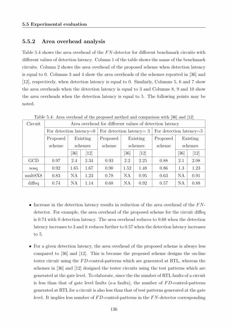
5.5 Experimental evaluation
5.5.2 Area overhead analysis
Table 5.4 shows the area overhead of the FN -detector for different benchmark circuits with
different values of detection latency. Column 1 of the table shows the name of the benchmark
circuits. Column 2 shows the area overhead of the proposed scheme when detection latency
is equal to 0. Columns 3 and 4 show the area overheads of the schemes reported in [36] and
[12], respectively, when detection latency is equal to 0. Similarly, Columns 5, 6 and 7 show
the area overheads when the detection latency is equal to 3 and Columns 8, 9 and 10 show
the area overheads when the detection latency is equal to 5. The following points may be
noted.
Table 5.4: Area overhead of the proposed method and comparison with [36] and [12]
Circuit Area overhead for different values of detection latency
For detection latency=0 For detection latency= 3 For detection latency=5
Proposed Existing Proposed Existing Proposed Existing
scheme schemes scheme schemes scheme schemes
[36] [12] [36] [12] [36] [12]
GCD 0.97 2.4 2.34 0.93 2.2 2.25 0.88 2.1 2.08
sosq 0.92 1.65 1.67 0.90 1.52 1.48 0.86 1.3 1.23
mult8X8 0.83 NA 1.23 0.78 NA 0.95 0.63 NA 0.91
diffeq 0.74 NA 1.14 0.68 NA 0.92 0.57 NA 0.88
• Increase in the detection latency results in reduction of the area overhead of the FN -
detector. For example, the area overhead of the proposed scheme for the circuit diffeq
is 0.74 with 0 detection latency. The area overhead reduces to 0.68 when the detection
latency increases to 3 and it reduces further to 0.57 when the detection latency increases
to 5.
• For a given detection latency, the area overhead of the proposed scheme is always less
compared to [36] and [12]. This is because the proposed scheme designs the on-line
tester circuit using the FD-control-patterns which are generated at RTL, whereas the
schemes in [36] and [12] designed the tester circuits using the test patterns which are
generated at the gate level. To elaborate, since the the number of RTL faults of a circuit
is less than that of gate level faults (s-a faults), the number of FD-control-patterns
generated at RTL for a circuit is also less than that of test patterns generated at the gate
level. It implies less number of FD-control-patterns in the FN -detector corresponding
136

5.6 Conclusion
to the RTL based representation, which results less area overhead compared to gate
level testing.
• In RTL, we can decide the invalid FD-control-patterns for a fault and drop them in
the design of the FN -detector circuit, thus the area overhead can be further reduced.
Whereas, in the case of gate level circuits there is no such feature to decide invalid test
patterns for a fault. So, in the gate level case, we include all the test patterns for a
fault in on-line tester design which increases the area overhead.
5.6 Conclusion
In this chapter, we have proposed a HLDD based OLT scheme for digital circuits at RTL
using different high level fault models. The proposed scheme mainly improves the scalability
aspect of OLT. Experimentally, it is shown that the test generation time of the proposed
scheme is much lower compared to the gate level techniques, thus, large circuits can be easily
handled. It is also observed that the scheme achieves comparable fault coverage with low
area overhead. The main reason for improvement in scalability is due to use of HLDD for
modeling the circuits at RTL and generation of the exhaustive set of FD-control-patterns.
Most of the OLT schemes including our techniques proposed in the Chapters 3, 4 and 5
are designed for synchronous circuits. However, now-a-days asynchronous circuits are being
used in the semiconductor industry, because of the advantages like no clock skew problem,
higher degree of modularity, low power consumption, average case performance, etc. Thus,
one of the challenges in OLT is to develop on-line testers for asynchronous circuits. In the
next chapter, we extend our work by designing an OBDD based OLT scheme for Speed
Independent asynchronous (SI) circuits.
137


Chapter 6
On-line Testing of Speed Independent
Asynchronous Circuits
6.1 Introduction
Since the last two decades synchronous circuits have widespread use in VLSI design whereas
asynchronous circuits have not been used in practice to that extent. However, compared
to synchronous circuits, asynchronous circuits promise a number of advantages such as
no clock skew problem, higher degree of modularity, low power consumption and average
case performances rather than worst case executions [111]. In recent years, the use of
the asynchronous circuits in the semiconductor industry has matured a lot because of the
above advantages. Testing of asynchronous circuits as compared to synchronous circuits
is considered difficult due to the absence of the global clock [50]. Also, On-line Testing
(OLT) of such circuits is one of the challenging tasks. It is seen that most of the OLT
schemes have been designed for synchronous circuits only. There are very few works that
have been proposed on OLT of asynchronous circuits [107,109,129]. The details about these
schemes can be found in Chapter 2, Subsection 2.3.4. The scheme proposed in [129] is based
on traditional full replication technique, thus, it leads to more than 100% area and power
overheads. The works reported in [107, 109] are based on checking of a predefined protocol
using Mutex elements. So, these schemes are protocol specific and use of Mutex elements
make area overhead of these techniques high.
In this chapter, we aim at developing an efficient OLT scheme for asynchronous circuits
which is protocol independent and incurs low area overhead. The proposed non-intrusive
OLT scheme is easily applicable to all type of Speed Independent asynchronous circuits (SI
circuits). The scheme starts with modeling of SI circuits along with their faults using Signal
139
6.2 SI circuit modeling using Signal Transition Graph and generation ofFD-transitions
Transition Graphs (STGs), then translating them into State Graphs (SGs), from which Fault
Detecting transitions (FD-transitions) are generated. In case of OLT of synchronous circuits,
the on-line tester circuit is a Finite State Machine (FSM) which detects the occurrence of FD-
transitions (the procedure is discussed in Chapters 3 and Chapter 4). A synchronous circuit
can be synthesized in a straightforward manner from the FSM specification that performs on-
line testing. In similar way a synchronous circuit can be synthesized as the on-line tester for
OLT of an asynchronous circuit, but the use of synchronous circuit for OLT of asynchronous
circuit is not desirable. So, we propose a new technique for design of on-line tester, called
Fault versus Normal condition detector (FN -detector), which can be synthesized as an SI
circuit. The tester is designed as state graph model which is live and has Complete State
Coding (CSC); these properties ensure its synthesizability as an SI circuit. Finally, we
discuss the procedure of generation of FD-transitions in an efficient manner directly from
the circuit description using Ordered Binary Decision Diagram (OBDD), without explicitly
constructing the SG models whose complexity may be prohibitively high for large circuits.
The chapter is organized as follows. In Section 6.2, we discuss the modeling of an
SI circuit using STG under normal and faulty conditions. Following that, conversion of
STGs into SGs and generation of FD-transitions are discussed. In Section 6.3, we illustrate
the design of the FN -detector using FD-transitions. Efficient generation of FD-transitions
using OBDD is discussed in Section 6.4. Section 6.5 presents experimental results regarding
area overhead and fault coverage of the FN -detector. Also, comparison of area overhead
of the proposed scheme with other similar techniques is reported. Finally, we conclude in
Section 6.6.
6.2 SI circuit modeling using Signal Transition Graph
and generation of FD-transitions
In this section, we start with modeling of an SI circuit using STG under normal and faulty
conditions, then convert the STGs into SGs and generate FD-transitions. Just like modeling
of synchronous circuits discussed in Chapter 3 and Chapter 4, the basic FSA framework is
also used to model asynchronous circuits with slight modification. In case of synchronous
circuits, state changes in the FSA occur only at the active edge of the register clock,
irrespective of the time of changes in the inputs. On the other hand, in asynchronous
circuits, state changes can occur immediately after a transition in the inputs. FSA used to
model an asynchronous circuit is called an AFSA (Asynchronous FSA) [80]. An alternative
to AFSA is Burst-mode (BM) state machines [80]. BM state machine and AFSA are similar
140

6.2 SI circuit modeling using Signal Transition Graph and generation ofFD-transitions
from the modeling perspective, however in case of the former, transitions are labeled with
signal changes rather than their explicit values, which is the case in AFSAs. AFSAs and
BM state machines assume that inputs change first followed by outputs and finally a new
state is reached. Due to the strict sequence of signal changes all asynchronous protocols
cannot be modeled using AFSAs or BM state machines. Petri net (PN) is widely accepted
modeling framework for highly concurrent systems [27]. PN models a system using interface
behaviors which are represented by allowed sequence of transitions or traces. The view of an
asynchronous circuit as a concurrent system makes PN based models more appropriate than
AFSAs and BM state machines for their analysis and synthesis. There are several variants of
PNs among which Signal Transition Graph (STG) is generally used to model asynchronous
circuits. The major reason is that the STG interprets transitions as signal transitions and
specifies circuit behavior by defining casual relations among these signal transitions [71].
The SI circuit shown in Figure 6.1 (taken from [71]) will be considered as Circuit Under
Test (CUT) to illustrate our proposed scheme. Traditionally synchronous circuits consist of
blocks of combinational logic connected with clocked latches or registers, while in case of
SI circuit designs, we basically have logic gates as building blocks with C-elements, which
act as storage elements. Transistor level diagram of C-element is shown in Figure 6.2; logic
function of the C-element can be described by the Boolean equation C = AB +AC ′ +BC ′,
where C is the next state and C ′ is the old state value [71, 106]. The output of C-element
becomes logically high (low) when both the inputs are logically high (low), otherwise it
keeps its previous logic value. There are two types of C-elements that are used in SI circuits;
static C-element and dynamic C-element. The static version of C-element promises that the
information inside it can be stored for unbounded periods. However, dynamic version of
C-element provides gains in terms of area, power and delay [77,105,106,120]. Since circuits
having high operating speed, low area and power consumption are preferred in modern days,
we have chosen SI circuits with dynamic C-elements instead of static ones.
Figure 6.3 shows the STG for the CUT being considered. Rising (falling) transitions on
signals, indicated by +(−), are shown in the STG. The dark circles along the arcs are called
tokens. A token indicates one of possibly a set of signals that enable a transition to fire.
If all input arcs for a signal transition have tokens then that signal transition is said to be
enabled. For example, when signal Rin goes high (denoted by Rin+) and signal Rout goes
high (denoted by Rout+), only then Aout+ transition can take place. Upon firing Aout+,
a token is placed on each of its outgoing arcs, thus enabling Rin−. Note that Rout− is
enabled after Aout+ and Ain+.
In this work we have considered SI circuits that contain C-elements (we assumed
141

6.2 SI circuit modeling using Signal Transition Graph and generation ofFD-transitions
C1
C2
Rin
Ain
Aout
5
6
10
1112
13
4
21
3 8
7
9
B
A
B
A
Rout
Figure 6.1: Example of speed independent circuit as CUT.
n1
p1
p2
n2
n3
p3
A
B
Vdd
C
Figure 6.2: Transistor diagram of dy-namic C-element.
Aout −
Rin +
Rin −
Aout +
Rout −
Ain −
Rout +
Ain +
Figure 6.3: Signal Transition Graph ofthe sample circuit (Figure 6.1).
142

6.2 SI circuit modeling using Signal Transition Graph and generation ofFD-transitions
dynamic version) and logic gates. For the logic gates, the most popular fault model is
the stuck-at (s-a) model. However, for the C-elements stuck-on and stuck-off faults for each
transistor is an accepted fault model [71]. So we have chosen a mixed gate/transistor level
description for modeling the faults. To illustrate fault modeling at both C-elements and
basic gates, we consider the circuit example from [71] which is shown in Figure 6.1. We first
model the faults in the gates and transistors (for the C-elements) and map them to STGs of
the circuit. For the analysis, the signals attached to the inputs A and B of the C-elements
are also indicated in the gate level circuit diagram of Figure 6.1. Now, we consider some of
these faults (one at a time), analyze their effects, and finally modify the STG to model the
faults.
Consider the C-element C2 of Figure 6.1 and refer to transistor level circuit of Figure 6.2.
The C-element C2 has Rout and Rin as inputs and Aout as output. If the transistor n1 has
a stuck-on fault, this leads to an error in the circuit, where it needs to wait for only n2 to
be enabled to generate the output. When n2 turns on, then a path to ground via n1 and n2
gets established, which makes p3 on and n3 off, making C high. So C2 has to wait only for
n2 (i.e., Rin+ which corresponds to input B of C2 to become 1) to turn on and change the
output. In other words, it has to wait for only Rin+ (and not also for Rout+, which is the
requirement under normal condition) before it can generate Aout+. Thus, the fault in n1
leads to premature firing of the Aout+ transition. We represent this by including a token
on the arc connecting Rout+ to Aout+. Availability of this token will enable Aout+ to fire
as soon as Rin+ arrives, without waiting for Rout+. This token is denoted by a ‘1’ shown
on the arc in Figure 6.4.
Now consider C-element C1 producing output Rout, with transistor p1 having stuck-on
fault. As p1 is on, the gate has to wait for p2 to turn on before it can change the output.
When p2 turns on (by virtue of B = 0) then there is no path to ground as n2 is off, which
makes p3 off and n3 on, making C low. Here, C1 has to wait for the input B = 0 to generate
Rout−. Referring to Figure 6.1, for B to become 0, we need either Aout to become 1 (same
as Rin becoming 0) or Ain to become 1. Thus, as soon as we have either Aout+ or Ain+,
Rout− would fire. It may be noted that under normal condition, for Rout− to fire, we also
require A = 0, which mandates both Aout+ and Ain+. This failure condition is indicated
in the STG by adding a ‘1’ to the input arcs of Rout−, which is shown in Figure 6.5. To
elaborate, Figure 6.5(a) (Figure 6.5(b)) shows that Rout− can be fired as soon as Ain+
(Aout+) fires and does not wait for Aout+ (Ain+).
As the third fault, let there be a stuck-on fault at n2 of C1. The stuck-on fault at n2
enforces the circuit to wait only for n1 to be enabled for generating output Rout+. As n1
143

6.2 SI circuit modeling using Signal Transition Graph and generation ofFD-transitions
Aout −
Rin +
Rin −
Aout +
Rout −
Ain −
Rout +
Ain +
1
Figure 6.4: STG representation of stuck-on fault in n1 of C2 (Figure 6.1).
Aout −
Rin +
Rin −
Aout +
Rout −
Ain −
Rout +
Ain +
1
(a) Rout- doesn’t wait for Aout+
Aout −
Rin +
Rin −
Aout +
Rout −
Ain −
Rout +
Ain +
1
(b) Rout- doesn’t wait for Ain+
Figure 6.5: STG representation of stuck-on fault in p1 of C1 (Figure 6.1).
144

6.2 SI circuit modeling using Signal Transition Graph and generation ofFD-transitions
Rin +
Rin −
Aout +
Rout −
Ain −
Rout +
Ain +
Aout −
1
Figure 6.6: STG representation of stuck-on fault in n2 of C1 (Figure 6.1).
is connected to input A, which is logical ORing of Aout− and Ain−, transition Rout+ can
fire after Aout− or Ain− (without requiring to wait for Rin+). This premature firing of
the transition Rout+ is indicated in the STG by adding a “1” to Rin+, which is shown in
Figure 6.6.
For the gates, s-a-0 and s-a-1 faults are considered at their input and output nets. Let
Line 2 of the AND gate from Figure 6.1 be affected by s-a-0 fault. This implies a s-a-0 fault
at Line 6. As Line 6 is connected to the B input of the C-element C1, we have transistor
p2 on and transistor n2 off. Note that, as n2 is always off, there is no path to the ground.
So the output Rout can never become 1, because p3 can never turn on. In other words,
we will never have the Rout+ transition. This is indicated by adding a ‘0’ on the output
arcs of Rout+ in Figure 6.7. If Line 9 gets s-a-1, this will lead to Line 3 and Line 5 being
affected by s-a-0 fault, further leading to Line 6 being s-a-0. As Line 6 is connected to the
B input of the C-element, we will have the fault manifestation similar to the case of Line 2
s-a-0. Now we consider a s-a-0 fault at Line 13. As this line is connected to the B input of
the C-element C2, it will lead to output Aout never becoming 1. That means, we will never
have Aout+ transition. The effect is shown by adding a ‘0’ to the output arcs of Aout+, in
Figure 6.8.
145

6.2 SI circuit modeling using Signal Transition Graph and generation ofFD-transitions
Aout −
Rin +
Rin −
Aout +
Rout −
Ain −
Rout +
Ain +
0
0
Figure 6.7: STG representation of s-a-0 faultin line-2 (Figure 6.1).
Aout −
Rin +
Rin −
Aout +
Rout −
Ain −
Rout +
Ain +
00
Figure 6.8: STG representation of s-a-0 faultin line-13 (Figure 6.1).
Now we consider an example of a redundant fault, i.e., no logical difference is observed
in the operation of the circuit after the fault. An instance of such a fault is n1 stuck-on fault
in C1. This fault enforces the circuit to wait only for n2 to be enabled (i.e., B to be 1) for
generating output Rout+. As n2 is connected to input B, which is logical ANDing of Rin+,
Aout− and Ain−, Rout+ can fire only after three transitions, viz. Rin+ and Aout− and
Ain− fire. It may be noted that Aout− and Ain− also imply that input A (connected to
n1) of C1 is 1, which in turn implies on condition for n1. As fault and normal condition both
implies n1 to be on, stuck-on fault at n1 of C1 do not generate any behavioral difference.
Obviously, such faults cannot be detected under the single s-a fault assumption.
For the fault model considered the total number of faults in an SI circuit having dynamic
C-elements is equal to 12 times the number of C-elements (each C-element consists of 6
transistors and each transistor can have stuck-on and stuck-off fault) plus twice the number
of I/O lines of the gates (each line has either s-a-0 or s-a-1 fault). So the number of faults
in case of the circuit considered in Figure 6.1 is not too small and listing them all would
make a tabular representation long. So a partial list of faults and their effects on the STG
are given in Table 6.1.
146

6.2 SI circuit modeling using Signal Transition Graph and generation ofFD-transitions
Table 6.1: A partial list of faults and their effects on STG
Fault Type Effect of fault on the transitions
Transistor n1 stuck-on fault for C1 Rout+ can only be fired after Rin+,
Aout- and Ain- (same as normal condition)
Transistor n2 stuck-on fault for C1 Rout+ can be fired after either Aout- or Ain-
Transistor p1 stuck-on fault for C1 Rout- can be fired after either Aout+ or Ain+
Transistor p2 stuck-on fault for C1 Rout- can only be fired after Aout+ and Ain+
Transistor n1 stuck-on fault for C2 Aout+ can be fired after Rin+
Transistor n2 stuck-on fault for C2 Aout+ can be fired after Rout+
Transistor p1 stuck-on fault for C2 Aout- can be fired after Rin-
Transistor p2 stuck-on fault for C2 Aout- can be fired after Rout-
Transistor n1 stuck-off fault for C1 All arcs from Rout+ always 0
Transistor n2 stuck-off fault for C1 All arcs from Rout+ always 0
Transistor p1 stuck-off fault for C1 All arcs from Rout- always 0
Transistor p2 stuck-off fault for C1 All arcs from Rout- always 0
Transistor n1 stuck-off fault for C2 All arcs from Aout+ always 0
Transistor n2 stuck-off fault for C2 All arcs from Aout+ always 0
Transistor p1 stuck-off fault for C2 All arcs from Aout- always 0
Transistor p2 stuck-off fault for C2 All arcs from Aout- always 0
Transistor n3 stuck-on fault for C1 All arcs from Rout+ always 0
Transistor p3 stuck-off fault for C1
Transistor p3 stuck-on fault for C1 All arcs from Rout- always 0
Transistor n3 stuck-off fault for C1
Transistor p3 stuck-on fault for C2 All arcs from Aout- always 0
Transistor n3 stuck-off fault for C2
Transistor n3 stuck-on fault for C2 All arcs from Aout+ always 0
Transistor p3 stuck-off fault for C2
S-a-0 fault at Line 1 All arcs from Rout+ always 0
or Line 2 or Line 3
S-a-0 fault at Line 6 or Line 7
S-a-1 fault at Line 9 or Line 10
S-a-0 fault at Line 4 and Line 5 All arcs from Rout+ always 0
S-a-1 fault at Line 4 or Line 5 All arcs from Rout- always 0
S-a-1 fault at Line 6 or Line 7
S-a-0 fault at Line 9 or Line 10
S-a-0 fault at Line 8 All arcs from Rout+ always 0
and All arcs from Aout+ always 0
S-a-1 fault at Line 8 All arcs from Rout- always 0 and
All arcs from Aout- always 0
S-a-0 fault at Line 11 All arcs from Rout- always 0
and All arcs from Aout+ always 0
147

6.2 SI circuit modeling using Signal Transition Graph and generation ofFD-transitions
S-a-1 fault at Line 11 All arcs from Rout+ always 0
and All arcs from Aout- always 0
S-a-0 fault at Line 12 or Line 13 All arcs from Aout+ always 0
S-a-1 fault at Line 12 or Line 13 All arcs from Aout- always 0
6.2.1 Converting STG into State Graph model and generation of
FD-transitions
A State Graph (SG) G is defined as G = 〈V,X,=, X0〉, where V = {v1, v2, ...., vn} 1 is a
finite set of Boolean variables, i.e., the domain of the variables is {0, 1}, X is a finite set of
states, = is a finite set of transitions and X0 ⊆ X is the set of initial states. A state x is
a mapping of each variable to one of its domain elements. A transition τ ∈ = from a state
x to another state x+ is an ordered pair 〈x, x+〉, where x is denoted as initial(τ) and x+ is
denoted as final(τ).
The stuck-on and stuck-off faults in the transistors of the C-elements of the circuit are
captured by dividing the SG into sub-models and each sub-model is used to describe the
system under normal or faulty conditions. To make differentiation among the sub-models,
each state x is assigned a fault label by a status variable C with it’s domain being equal to
{N ∪F1 ∪F2 ∪ ....∪Fp}, where N is the normal status, Fi, 1 ≤ i ≤ p, is the fault status and
p is the number of possible faults.
Definition 6.1. Normal G-state: A G-state x is normal if x(C) = N . The set of all
normal states is denoted as XN .
Definition 6.2. Fi-G-state: A G-state x is fault state, or synonymously, an Fi-state, if
x(C) = Fi. The set of all Fi-states is denoted as XFi.
Definition 6.3. Normal-G-transition: A G-transition 〈x, x+〉 is called a normal G-
transition if x, x+ ∈ XN .
Definition 6.4. Fi-G-transition: A G-transition 〈x, x+〉 is called an Fi-G-transition if
x, x+ ∈ XFi.
Definition 6.5. Equivalent states: Two states x and y are said to be equivalent, denoted
as xEy, if x|V = y|V and x(C) 6= y(C).
In other words two states are said to be equivalent if they have same values for state variables
and different value for status variable.
1In case of modeling SI circuits as SG, the state variables are values of the I/O signals. So in this work,
we will interchangeably use the terms signal and variable.
148

6.2 SI circuit modeling using Signal Transition Graph and generation ofFD-transitions
A transition 〈x, x+〉, where x(C) 6= x+(C), is called an si-transition (start of fault Fi),
indicating the first occurrence of fault Fi in the circuit. Faults are assumed to be permanent.
Definition 6.6. Equivalent transitions: Two transitions τ1 = 〈x1, x+1 〉 and τ2 = 〈x2, x
+2 〉
are equivalent, denoted as τ1Eτ2, if x1Ex2 , x+1 Ex+
2 and they must associate with same signal
change.
Suppose there is a transition in faulty SG sub-model for which there is no corresponding
equivalent transition in the normal SG sub-model, then that transition is called Fault
Detecting transition (FD-transition). The fault is detected when the system traverses
through the FD-transition. Thus, we can define FD-transition as:
Definition 6.7. FD-transition: An Fi-G-transition of faulty SG sub-model τ ′ = 〈x′, x′+〉is an FD-transition, if there is no G-transition τ = 〈x, x+〉 in the normal SG sub-model
such that τ ′Eτ .
As already discussed, the first step of state based OLT is to generate normal and faulty
models. For SI circuits, the STGs under normal and faulty conditions are obtained and then
converted into separate SG models. We explain the concept using the example circuit of
Figure 6.1 under normal and two faults, namely, stuck-on fault in n1 of C2 and stuck-on
fault in p1 of C1.
The SG sub-model for the normal circuit is shown in Figure 6.9. It may be noted
that in the circuit there are 4 I/O signals namely, Rin,Rout,Ain,Aout. In the SG model
corresponding to each signal there is a discrete variable: 〈v1 = Rin, v2 = Rout, v3 =
Ain, v4 = Aout〉 which assumes values from the set {0, 1}. The set of states are X0 to
X13 and X0 is the initial state. State mappings and transitions are shown in Figure 6.9;
e.g., state X0 maps variables 〈Rin,Rout, Ain,Aout〉 to 〈1, 1, 0, 0〉. In states X0 and X1 the
mappings are 〈1, 1, 0, 0〉 and 〈1, 1, 0, 1〉, respectively. So transition from X0 to X1 changes
Aout from 0 to 1; this is indicated by the transition Aout+. Now, if we look at the STG
for the normal circuit shown in Figure 6.3, we note that Aout+ can fire if Rin+ and Rout+
have a token (i.e., Rin = 1 and Rout = 1). In state X0 as Rin = 1 and Rout = 1, so Aout+
can fire. Similarly, the whole SG is constructed.
The SG sub-model for the circuit under n1 stuck-on fault in C2 is shown in Figure 6.10.
The set of states are X ′0 to X ′13 and X ′0 is the initial state. The transitions and state
mappings are shown in the figure. As discussed in the previous section, n1 stuck-on fault
in C2 results in premature firing of Aout+ (i.e., it need not wait for Rout+ and can fire
only if Rin+ holds). If we observe the faulty SG sub-model shown in Figure 6.10, we note
that there are two dotted transitions, which correspond to the fault condition i.e., premature
149

6.2 SI circuit modeling using Signal Transition Graph and generation ofFD-transitions
1010
1011
0001
Aout+
Rin+
Aout−
Ain−
Rout−
Ain+
Rin−
1101
0101
1110
1111
0111
0011
0010
1000
0000
1001
Rout+
X0
1100
X1
X4
X2
X5 X6
X7 X8
X10X9
X11 X12
X13
X3
Ain+
Ain+
Rin−
Rout− Rin−
Rin−
Aout−Ain−
Rin+Ain−
Aout+
Ain−
Figure 6.9: SG sub-model for the normal circuit (STG of Figure 6.3)
1010
1011
0001
Aout+
Rin+
Aout−
Ain−
Rout−
Ain+
Rin−
1101
0101
1110
1111
0111
0011
0010
1000
0000
1001
Rout+
X’0
1100
X’1
X’4
X’2
X’5 X’6
X’7 X’8
X’10X’9
X’11 X’12
X’13
X’3
Ain+
Ain+
Rin−
Rout− Rin−
Rin−
Aout−Ain−
Rin+Ain−
Aout+
Ain−
Aout+
Aout+
Figure 6.10: SG sub-model for the circuit with n1 stuck-on fault in C2 (STG of Figure 6.4).
150

6.2 SI circuit modeling using Signal Transition Graph and generation ofFD-transitions
1010
1011
0001
Aout+
Rin+
Aout−
Ain−
Rout−
Ain+
Rin−
1101
0101
1110
1111
0111
0011
0010
1000
0000
1001
Rout+
X"0
1100
X"1
X"4
X"2
X"5 X"6
X"7 X"8
X"10X"9
X"11 X"12
X"13
X"3
Ain+
Ain+
Rin−
Rout− Rin−
Rin−
Aout−Ain−
Rin+Ain−
Aout+
Ain−
Rout−
Rout−
Figure 6.11: SG sub-model for the circuit with p1 stuck-on fault in C1 (STGs of Figure 6.5).
firing of Aout+. One dotted transition is between X ′11 and X ′6. It may be noted that in
X ′11 we have Rin = 1, Rout = 0, Ain = 1 and Aout = 0; where, even though Rout+ is not
enabled, Aout+ fires because Rin+ is enabled. A similar premature firing of Aout+ occurs
between X ′13 and X ′8. So, for the fault n1 stuck-on in C2, there are two FD-transitions
namely, 〈X ′11, X ′6〉 and 〈X ′13, X ′8〉.
The SG sub-model for the circuit under p1 stuck-on fault in C1 is shown in Figure 6.11.
The set of states are X ′′0 to X ′′13 and X ′′0 is the initial state. As discussed in the previous
sub-section, p1 stuck-on fault in C1 results in premature firing of Rout− triggered by either
Ain+ or Aout+. This is captured by the dotted transitions 〈X ′′2, X ′′11〉 and 〈X ′′1, X ′′8〉 infaulty SG sub-model in Figure 6.11. The transition 〈X ′′2, X ′′11〉 represents firing of Rout−by Ain+ in spite of Aout+ not being enabled and the transition 〈X ′′1, X ′′8〉 represents firingof Rout− by Aout+ in spite of Ain+ not being enabled. Thus, for this fault there are two
FD-transitions namely, 〈X ′′2, X ′′11〉 and 〈X ′′1, X ′′8〉. The entire set of FD-transitions is
shown in Table 6.2.
In the next section, we shall discuss the procedure for design of the on-line tester called
FN -detector using FD-transitions and its synthesis as an SI circuit.
151
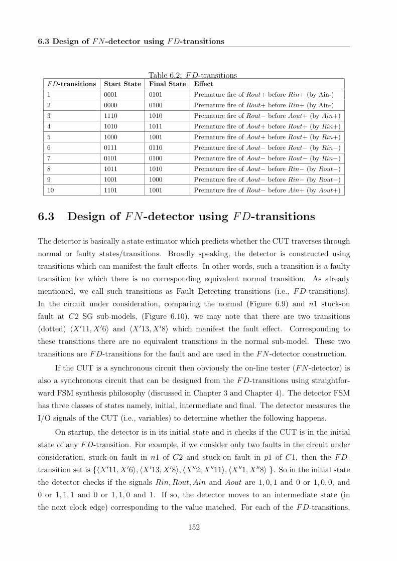
6.3 Design of FN-detector using FD-transitions
Table 6.2: FD-transitionsFD-transitions Start State Final State Effect
1 0001 0101 Premature fire of Rout+ before Rin+ (by Ain-)
2 0000 0100 Premature fire of Rout+ before Rin+ (by Ain-)
3 1110 1010 Premature fire of Rout− before Aout+ (by Ain+)
4 1010 1011 Premature fire of Aout+ before Rout+ (by Rin+)
5 1000 1001 Premature fire of Aout+ before Rout+ (by Rin+)
6 0111 0110 Premature fire of Aout− before Rout− (by Rin−)7 0101 0100 Premature fire of Aout− before Rout− (by Rin−)8 1011 1010 Premature fire of Aout− before Rin− (by Rout−)9 1001 1000 Premature fire of Aout− before Rin− (by Rout−)10 1101 1001 Premature fire of Rout− before Ain+ (by Aout+)
6.3 Design of FN-detector using FD-transitions
The detector is basically a state estimator which predicts whether the CUT traverses through
normal or faulty states/transitions. Broadly speaking, the detector is constructed using
transitions which can manifest the fault effects. In other words, such a transition is a faulty
transition for which there is no corresponding equivalent normal transition. As already
mentioned, we call such transitions as Fault Detecting transitions (i.e., FD-transitions).
In the circuit under consideration, comparing the normal (Figure 6.9) and n1 stuck-on
fault at C2 SG sub-models, (Figure 6.10), we may note that there are two transitions
(dotted) 〈X ′11, X ′6〉 and 〈X ′13, X ′8〉 which manifest the fault effect. Corresponding to
these transitions there are no equivalent transitions in the normal sub-model. These two
transitions are FD-transitions for the fault and are used in the FN -detector construction.
If the CUT is a synchronous circuit then obviously the on-line tester (FN -detector) is
also a synchronous circuit that can be designed from the FD-transitions using straightfor-
ward FSM synthesis philosophy (discussed in Chapter 3 and Chapter 4). The detector FSM
has three classes of states namely, initial, intermediate and final. The detector measures the
I/O signals of the CUT (i.e., variables) to determine whether the following happens.
On startup, the detector is in its initial state and it checks if the CUT is in the initial
state of any FD-transition. For example, if we consider only two faults in the circuit under
consideration, stuck-on fault in n1 of C2 and stuck-on fault in p1 of C1, then the FD-
transition set is {〈X ′11, X ′6〉, 〈X ′13, X ′8〉, 〈X ′′2, X ′′11〉, 〈X ′′1, X ′′8〉 }. So in the initial state
the detector checks if the signals Rin,Rout, Ain and Aout are 1, 0, 1 and 0 or 1, 0, 0, and
0 or 1, 1, 1 and 0 or 1, 1, 0 and 1. If so, the detector moves to an intermediate state (in
the next clock edge) corresponding to the value matched. For each of the FD-transitions,
152

6.3 Design of FN-detector using FD-transitions
there is a corresponding intermediate state in the detector. For example, if Rin,Rout, Ain
and Aout are measured to be 1, 0, 1 and 0 in the initial state of the detector, the detector
moves to the intermediate state corresponding to FD-transition 〈X ′11, X ′6〉. However, if
the signals do not match the initial state of any FD-transition the detector loops in the
initial state. In the intermediate state whether the values of the signals of the CUT match
with the final state of the corresponding FD-transition is checked; if so, the fault is detected
and the detector moves to the final state and is deadlocked there. Otherwise, it moves to
the initial state. Continuing with the example, if the values of Rin,Rout, Ain and Aout are
1, 0, 1 and 1 respectively, from the intermediate state, FD-transition 〈X ′11, X ′6〉 is detected(i.e., stuck-on fault in n1 of C2) and the detector moves to the final state in the next clock
edge. Otherwise, if Rin,Rout, Ain and Aout are 1, 0, 0 and 0 then CUT is normal and the
detector moves to the initial state.
The above mentioned philosophy of constructing the detector and then synthesizing it
into a synchronous system is widely used in OLT of synchronous circuits [10,12]. Obviously,
if the CUT is an SI circuit, so must be the detector circuit. However, it may be noted that
the same philosophy cannot be directly used in the case of SI circuits. The reason is, the
FSM of the detector designed above has liveness issue in the final state and has Complete
State Coding (CSC) violations in the intermediate states. In this work, we propose a new
technique for detector design which can be synthesized as an SI circuit. The detector is
designed as state graph model which is live and has CSC, that ensure its synthesizability as
an SI circuit. Before formalizing the algorithm for the design of the State Graph (SG) of
the detector, we first introduce the basic philosophy of its working using the examples from
the previous section.
An FD-transition in SI circuit design paradigm can be stated as “under fault, a signal
s can change in the presence of signals y1, y2 · · · yn, (1 ≤ n) that is not possible under
normal condition”. For example, in the case of n1 stuck-on fault of C2, 〈X ′11, X ′6〉 is an
FD-transition which changes signal Aout from 0 to 1 (i.e., Aout+) and the other signals are
Rin = 1, Rout = 0, and Ain = 1 (Figure 6.10). It may be noted that in normal condition
(shown in Figure 6.9) for changing Aout from 0 to 1 we need Rin = 1, Rout = 1, and
Ain = 0 (in state X0) and Rin = 1, Rout = 1, and Ain = 1 (in state X2). Comparing
with the faulty condition we may state that “under n1 stuck-on fault of C2, signal Aout
can change from 0 to 1 in presence of signals Rin = 1, Rout = 0, and Ain = 1 which is
not possible under normal condition”. So, to detect whether FD-transition 〈X ′11, X ′6〉 hasoccurred, the detector needs to tap lines Rout and Aout (Rin and Ain are not required
to be monitored as their values are same under normal and faulty cases) of the CUT and
153

6.3 Design of FN-detector using FD-transitions
determine whether Aout+ has fired and at that time whether Rout = 0; if so, a status output
line is made 1. If we consider the other FD-transition 〈X ′13, X ′8〉 for the fault, it can be
detected by checking if Aout+ has fired and at that time whether Rout = 0; Rin,Ain are
not required to be monitored as their values are same under normal and faulty cases. So,
it may be stated that to detect the fault by FD-transitions 〈X ′11, X ′6〉 and 〈X ′13, X ′8〉 weneed to check whether Aout+ has fired and at that time whether Rout = 0. Figure 6.12
illustrates the SG for detecting n1 stuck-on fault at C2 by FD-transitions 〈X ′11, X ′6〉 and〈X ′13, X ′8〉. The design and flow of the detector for these two FD-transitions are as follows:
1. The state encoding tuple is 〈Rout, Aout, Status〉. The initial state of the detector z0 isencoded as 100. The first two bits represent the complement of Rout = 0 and Aout = 1
i.e., complement of the value of Rout in state X ′11 and complement of the change of
Aout by the FD-transition. The third bit represents Status output of the detector
which is 0 until FD-transition is detected.
2. The detector waits for signal Rout to become 0 and if so, it moves to state z1 say,
which is encoded as 〈000〉. However, from state z0, if Aout becomes 1, FD-transition
cannot be detected because this is normal situation (state X0 in Figure 6.9) where
Aout+ fires when Rout = 1; detector moves to state z5 having encoding 〈110〉. When
Aout becomes 0 in state z5, the detector moves back to z0 from where it again waits
to detect whether the FD-transition occurs.
3. From state z1 the following may happen:
(a) If Rout becomes 1, then FD-transition cannot be detected and so the detector
moves back to z0.
(b) If Aout becomes 1, then FD-transition has occurred and hence, fault is detected.
The detector moves to state z2 having encoding 〈010〉. Following that, the detectormakes Status output high and moves to state z3 with encoding 〈011〉.Once Status line is 1 i.e., fault is detected on-line, the system should switch to
an alternative backup circuit, as under the single stuck-at fault model faults are
assumed to be permanent [71]. By that logic, the detector should stop or loop in
z3 indefinitely, however, it would lead to deadlock and is non-synthesizable as an
SI circuit. To avoid this deadlock a simple modification is made in the detector
SG without effecting the fault detection performance. We wait at state z3 for any
signal to change (i.e., Rout from 0 to 1 or Aout from 1 to 0) and we move to state
z4; let us select Rout for this purpose. State encoding of z4 is 〈111〉. From state
z4 we have a transition to state z3 on change of Rout from 1 to 0.
154

6.3 Design of FN-detector using FD-transitions
z0 z1z2
z3 z4
z5
000 010 011 111
110
100
Rout−
Rout+
Aout+ Status+
Rout+
Rout−Aout+Aout−
State encoding tuple <Rout, Aout, Status>
Figure 6.12: SG for detecting the FD-transitions 〈X ′11, X ′6〉 and 〈X ′13, X ′8〉
In similar way we can design SGs for the other FD-transitions shown in Table 6.2.
However, it may be noted that different circuits may be required for the other FD-transitions
because merging all FD-transitions in a single detector SG will lead to CSC problems.
As shown in the example above, some FD-transitions can be merged into a single SG
maintaining CSC. Figures 6.13, 6.14, 6.15 and 6.16 given below illustrate the SGs for some
FD-transitions shown in Table 6.2. Also, the FD-transitions which could be merged are
mentioned in the figures.
z0 z1z2
z3 z4
z5
000 010 011 111
110
100
Rin−
Rin+
Rout+ Status+
Rin+
Rin−Rout+Rout−
State encoding tuple <Rin, Rout, Status>
Figure 6.13: SG for detecting the FD-transitions–Sl. No. 1 and 2 of Table 6.2
Before discussing the algorithm for generating the detector SGs for a set of FD-
transitions, we introduce the notion of compatible FD-transitions.
Definition 6.8. Compatible FD-transitions: Two FD-transitions τ ′1 = 〈X ′1, X ′1+〉and τ ′2 = 〈X ′2, X ′2+〉 are compatible if the following holds:
• If s1 is the signal change by τ ′1 and s2 is the signal change by τ ′2, then s1 is same as
s2. In other words, signal change by both the FD-transitions are same.
155

6.3 Design of FN-detector using FD-transitions
z0 z1z2
z3 z4
z5
010 000 001 101
100
110
Aout−
Aout+
Rout− Status+
Aout+
Aout−Rout−Rout+
State encoding tuple <Aout, Rout, Status>
Figure 6.14: SG for detecting the FD-transition–Sl. No. 3 of Table 6.2
z0 z1z2
z3 z4
z5
110 100 101 001
000
010
Rout+
Rout−
Aout− Status+
Rout−
Rout+Aout−Aout+
State encoding tuple <Rout, Aout, Status>
Figure 6.15: SG for detecting the FD-transitions–Sl. No. 6 and 7 of Table 6.2
z0 z1z2
z3 z4
z5
110 100 101 001
000
010
Rin+
Rin−
Status+
Rin−
Rin+Aout−Aout+
State encoding tuple <Rin, Aout, Status>
Aout−
Figure 6.16: SG for detecting the FD-transitions–Sl. No. 8 and 9 of Table 6.2
156

6.3 Design of FN-detector using FD-transitions
• Let V ′1 ⊆ V (for FD-transition τ ′1 = 〈X ′1, X ′1+〉) be the set of variables whose values
at X ′1 are different compared to state(s) Xi, where Xi is any state under normal
condition (normal sub-model) from which s1 is the signal change. Similarly, the set
V ′2 ⊆ V is calculated for FD-transition τ ′2 = 〈X ′2, X ′2+〉. Then V ′1 ∩ V ′2 6= φ. In
other words, there exists at least one signal (i.e., a variable) whose value is same in
the initial states of both the FD-transitions and that is different compared to the initial
state(s) of the corresponding transition(s) under normal condition.
For example, consider two FD-transitions 〈X ′11, X ′6〉 (= τ ′1, say) and 〈X ′13, X ′8〉(= τ ′2, say). We calculate V ′1 for τ ′1 as follows. The value of the variables at the initial
state X ′11 are {Rin = 1, Rout = 0, Ain = 1, Aout = 0}. The signal change for = τ ′1
is Aout+. We get two states (X0 = {Rin = 1, Rout = 1, Ain = 0, Aout = 0} and
X2 = {Rin = 1, Rout = 1, Ain = 1, Aout = 0}) in normal condition from which the signal
change Aout+ occurs. Thus, V ′1 = {Rout(= 0)} because Rout is the only variable that is
different in X ′11 compared to normal states X0 and X2. Similarly, we calculate V ′2 for τ ′2
as V ′2 = {Rout(= 0)}. Since V ′1 ∩ V ′2 6= φ = {Rout(= 0)}, thus, these two transitions are
compatible and can be merged (as shown in SG of Figure 6.12). Algorithm 6.1 is used to
construct SGs for the given set of FD-transitions.
6.3.1 Circuit synthesis for FN-detector
It is clear from the construction of the SGs of the detectors that they have Complete State
Coding (CSC) [26,69] and are live. So they can be synthesized as SI circuits using C-elements
and logic gates by applying standard asynchronous circuit synthesis procedures [23,45].
Figure 6.17 illustrates some snapshots regarding the steps of synthesizing the SG of
the detector shown in Figure 6.14 using the CAD tool Petrify [28]; Figure 6.17(a) is the
description of the SG that is given as input to Petrify, Figure 6.17(b) illustrates the output
of Petrify showing CSC and no liveness issues, and Figure 6.17(c) shows the equations
obtained from Petrify. The circuit schematic (of the detector) that is synthesized for this
SG is shown in Figure 6.18.
Now we explain some details of the Petrify equations. INORDER is a keyword of
Petrify to represent all I/O signals of the corresponding SG. OUTORDER is the keyword to
represent the output signals of the SG. Each subsequent line (denoted as [0], [1]...) represents
a gate of the circuit in terms of the function it implements. In case of the circuit of
Figure 6.18, INORDER = Aout,Rout, Status and OUTORDER = Status. The equations
[0] = Aout′Rout′ and [1] = 0 represent the logic expressions of the internal Gate 4 and Gate
157

6.3 Design of FN-detector using FD-transitions
(a) State graph (b) Output of Petrify
(c) Output equations of Petrify
Figure 6.17: Screenshot showing the synthesis of on-line detector from SG using Petrify
C
Aout
Rout
Logic 0
Status
1
2
3
4
5
6
7
Figure 6.18: FN -detector circuit for the SG shown in Figure 6.14
158

6.3 Design of FN-detector using FD-transitions
Algorithm 6.1 Algorithm for construction of detector SGs given the set of FD-transitionsInput: =FD: Set of FD-transitions
Output: Detector SGs for determining occurrence of FD-transitions
1. Partition =FD into compatible classes. Let =1FD,=2FD, · · · =lFD be the sets generated.
2. For each of these sets (=iFD, (1 ≤ i ≤ l)) generate a detector SG using the Step (3) to Step
(10).
3. s is the signal changed by τ ′ ∈ =iFD and y is any signal whose value is the same in initial
states of all τ ′ ∈ =iFD. Further, signal y is different in the initial state of the corresponding normal
transition that also makes same change in s.
4. Let state encoding of the detector be the tuple 〈y, s, Status〉.5. Create the initial state z0. The values of the variables in z0 are as follows: (i) y in the tuple for
z0 is complement of the value of the variable y in initial(τ ′),τ ′ ∈ =iFD, (ii) s in the tuple for z0 is
complement of the value of the variable s after its change by τ ′ ∈ =iFD, (iii) Status in z0 is 0.
6. Create state z1, with transition from z0 to z1 labeled as y+ (y−) if value of y in z0 is 0 (1). Also,
create a transition from z1 to z0 labeled with inverse of the signal change as in transition from z0
to z1. Accordingly encode state z1.
7. Create state z2, with transition from z1 to z2 labeled as s+ (s−) if value of s in z1 is 0 (1).
Accordingly encode state z2.
8. Create state z3, with transition from z2 to z3 labeled as Status+. Accordingly encode state z3.
9. Create state z4, with transition from z3 to z4 labeled as y+ (y−) if transition from z0 to z1 is
y− (y+). Add a transition from z4 to z3 with inverse of the signal change as in transition from z3
to z4. Accordingly encode state z4.
10. Create state z5, with transition from z0 to z5 labeled as s+ (s−) if transition from z1 to z2 is
s+ (s−). Add a transition from z5 to z0 with inverse of the signal change as in transition from z0
to z5. Accordingly encode state z5.
3, respectively. The equation [Status] = [1]′([0] + Status) + Status[0] represents the output
of the circuit.
In similar way, all SGs for the FD-transitions have been synthesized into different
circuits. Then the final on-line tester circuit (called FN -detector) for CUT is constructed
by simply ORing the outputs of these circuits. The output of the FN -detector becomes high
when output of at least one individual detector becomes high, thereby detecting the fault.
Till now in this chapter, the procedure of generation of FD-transitions for the design of
the FN -detector using SG model has been discussed. The procedure of generation of FD-
transitions involves−i) modeling the SI circuit under normal and faulty conditions using
STGs, ii) converting the STGs into SG sub-models, and iii) comparing each transition under
normal and faulty SG sub-models. This process of generating FD-transitions from the SG
159

6.4 Efficient generation of FD-transitions directly from circuit description usingOBDD
framework becomes complex for large circuits because the number of states in the SG model
grows exponentially with the variables/ signals of the circuit. Further, comparing each
transition under normal and faulty sub-models in order to generate FD-transitions is a time
taking task. In order to solve these problems we have devised a procedure which is capable
of generating FD-transitions directly from the circuit description using OBDDs, without
need of the explicit SG models.
6.4 Efficient generation of FD-transitions directly from
circuit description using OBDD
In this section, we discuss the procedure of generation of FD-transitions using OBDD based
operations in detail. The steps are similar to our proposed works discussed in Chapter 3,
Section 3.3 and Chapter 4, Section 4.3 with slight modifications. We first demonstrate the
procedure of generation of FD-transitions using an example, following that the detailed
procedure is discussed.
Consider n1 stuck-on fault of C2 (say F1) in the circuit shown in Figure 6.1, which
leads to premature firing of Aout+ transition. The STG model of the fault is shown in
Figure 6.4 where Aout+ is fired as soon as Rin+ fires, without waiting for Rout+. In other
words, we can say that under this fault Rout+ is always true, (i.e., Rout = 1) and whenever
Rin+ occurs in the circuit then Aout+ occurs. Since Aout is the output of C2, thus the
Boolean expression for Aout under normal condition is RinRout + RoutAout′ + RinAout′
(say Aoutnormal). Similarly, the Boolean expression for Aout under n1 stuck-on fault of
C2 is Rin + Aout′ (say Aoutfaulty), which is obtained by substituting Rout = 1 in the
normal Boolean expression (i.e., Aoutnormal). The OBDD representation of Aoutnormal =
RinRout + RoutAout′ + RinAout′ is shown in Figure 6.19 and the OBDD representation
of Aoutfaulty = Rin + Aout′ is shown in Figure 6.20. Figure 6.21 represents the OBDD
corresponding to Aoutnormal ⊕ Aoutfaulty which is obtained by XORing the normal and
faulty OBDDs illustrated in Figure 6.19 and Figure 6.20, respectively. The set of next states
under faulty condition which are different compared to the normal condition is obtained
by applying “satisfy-all-1” operation on the XORed OBDD, which is shown in Figure 6.21.
In case of F1, the set of next states obtained from “satisfy-all-1” operation on the XORed
OBDD is {〈Rin = 1, Rout = 0, Ain = 0, Aout = 1〉, 〈Rin = 1, Rout = 0, Ain = 1, Aout =
1〉, 〈Rin = 0, Rout = 0, Ain = 0, Aout = 0〉, 〈Rin = 0, Rout = 0, Ain = 1, Aout = 0〉}. Sincethe effect of fault F1 is premature firing of Aout+, so the value of Aout in the next states must
be equal to 1. Therefore, we have considered the next states where Aout = 1. Now the set of
160

6.4 Efficient generation of FD-transitions directly from circuit description usingOBDD
next state becomes as {〈Rin = 1, Rout = 0, Ain = 0, Aout = 1〉, 〈Rin = 1, Rout = 0, Ain =
1, Aout = 1〉}. Corresponding to the next state 〈Rin = 1, Rout = 0, Ain = 0, Aout = 1〉,the start/present state is 〈Rin = 1, Rout = 0, Ain = 0, Aout = 0〉 and the FD-transition is
〈1000, 1001〉. Similarly, corresponding to the next state 〈Rin = 1, Rout = 0, Ain = 1, Aout =
1〉, the present state is 〈Rin = 1, Rout = 0, Ain = 1, Aout = 0〉 and the FD-transition is
〈1010, 1011〉. The same was found in the SG model for n1 stuck-on fault in C2 (shown
Figure 6.10).
Rin
Rout Rout
Aout
1 0
0 1
0 1
1 0
1 0
Figure 6.19: Normal OBDD forAoutnormal
Rin
Aout
0
1
10
01
Figure 6.20: Faulty OBDDfor Aoutfaulty
Next we discuss the procedure for applying OBDDs for generation of FD-transitions
for a given fault (say Fi). Initially, the effect of the Fi is found from the STG model of the
fault. Let signal vk be one of the affected signals for the fault Fi which fires prematurely.
The following steps are used to generate FD-transitions to detect the premature fire of vk
due to the fault Fi.
1. Find the Boolean expression for vk from the circuit description under normal condition
(say vknormal). Generate OBDD for vknormal
. Let this OBDD be termed as “normal
OBDD”.
2. Find the Boolean expression for vk from the circuit description under fault Fi (say
vkFi). Generate OBDD for vkFi
. Let this OBDD be termed as “faulty OBDD”.
161

6.4 Efficient generation of FD-transitions directly from circuit description usingOBDD
Rin
Rout Rout
Aout Aout
01
0 1
0 1 0 1
010
1
Figure 6.21: XOR OBDD for the normal and faulty OBDDs
3. The two OBDDs (normal and faulty) are XORed and “satisfy-all-1” operation is
applied on the resulting XORed OBDD. This operation on the XORed OBDD generates
the set of next states that are attained by the CUT on firing of vk (rising or falling)
signal under faulty Fi. Let NSvk be the set of such next states.
4. If Fi affects the rising signal of vk, i.e., vk+, then remove the states from NSvk where
the value of vk is 0. Let NSvk+ be the set of such next states.
5. If Fi affects the falling signal of vk, i.e., vk−, then remove the next states from NSvk
where the value of vk is 1. Let NSvk− be the set of such next states.
6. Once the required set of next states (either NSvk+ or NSvk−) is determined, then
for each state ns ∈ NSvk+ (NSvk−), its corresponding start/present state (say, ps)
is obtained by changing only the value of vk in ns from 1 (0) to 0 (1) and other
signal values remain unchanged. Finally, for each state ns ∈ NSvk+ (NSvk−), an
FD-transition is generated which includes both start/present state and next state as
〈ps, ns〉, which detects the occurrence fault Fi in the CUT.
162

6.5 Experimental evaluation
6.5 Experimental evaluation
To validate the efficacy of the scheme we analyze the area overhead ratio of the FN -detector
to that of the CUT. Further, we also compare the overhead with other techniques reported in
the literature. In our experiments we have considered some standard SI benchmark circuits
[44]. Further, for comparison we have also implemented our scheme on the circuits used in
[107].
The algorithm discussed in previous section is used to design a CAD tool OLT-ASYN which
generates the FN -detector for OLT given an asynchronous circuit specification. We calculate
performance parameters as follows.
Fault Coverage (FC): FC = (Number of faults covered)/(Total number of faults) × 100
Area Overhead (AO): AO= (Area of the FN -detector after synthesis)/(Area of the CUT)
Table 6.3 shows the number of gates, number of faults, fault coverage, area overhead
ratio and execution time of the proposed approach for the different SI circuits being
considered. The first three circuits in the table are simple examples whose gate level designs
are shown in Figure 6.22, Figure 6.23 and Figure 6.24. The fourth and fifth circuits have been
used in [107]. The others are standard asynchronous benchmarks [44] which are complex
in terms of area, states and number of signals compared to first five circuits in the table.
Broadly speaking, it can be observed in Table 6.3 that area overhead decreases with the
increase of the size of the circuit. In [35], Drineas et al. have identified that the area
overhead ratio for partial replication based OLT for s-a faults is approximately α + 1/β,
where α is the fraction of test patterns incorporated in detector design (α=1 when all FD-
transitions are incorporated in detector design) and β is the number of state bits required
for circuit representation (i.e., proportional to the circuit size). In this work we have taken
all possible FD-transitions and the obtained area overhead ratio acts (approximately) in
accordance with the fact mentioned above.
From the discussion in the last section regarding design of the detector from the FD-
transitions it may appear that a large number of such detectors may be required for complex
circuits. In the worst case the number of detectors may be equal to the number of FD-
transitions. Further, in case of large circuits as the number of nets and C-elements are
high the number FD-transitions may be proportionally large. However, interestingly, the
experiments illustrated reverse trends. Large circuits have high number of possible s-a faults,
however, many of them are mapped to similar effects and hence same FD-transitions; this
can be observed from Table 6.1 for the running example. Further, using the principle of
compatible of FD-transitions, it was found that multiple FD-transitions fall in the same
cluster thereby resulting in the fact that a single detector suffices for more than one FD-
163

6.5 Experimental evaluation
transition. To conclude, it was observed that a few detectors are actually required to cover all
the faults. To the best of our knowledge such facts regarding OLT of asynchronous circuits
were not reported in the literature.
It may be noted that percentage of fault coverage is more than 95% on the average. The
number of faults that could not be detected were found to be redundant.
Table 6.3: Fault coverage, area overhead ratio and execution time for the FN -detectordesigned using the proposed approach
Circuits Number of Number of % of fault Area Execution
gates faults coverage overhead time(sec)∗
Circuit 1 3 22 95 0.8 0.12
Circuit 2 5 32 96 1.5 0.23
Circuit 3 5 54 98 1.2 0.34
2 David cells [107] 6 44 94 1.6 0.22
4 David cells [107] 12 88 93 1 0.40
chu172 9 47 96 0.24 0.36
alloc-outbound 15 130 98 0.13 0.42
sbuf-read-ctl 19 152 95 0.12 0.51
sbuf-send-ctl 18 140 94 0.087 0.47
ram-read-sbuf 23 197 93 0.025 0.56
∗Executed in AMD Phenom (tm) IIX3 710 Processor with 4GB RAM in Linux OS
a1
r1
a2
r2
Figure 6.22: Circuit 1
c
Cc
a
b
Figure 6.23: Circuit 2
6.5.1 Mutex approach to testing [107]
Now we will discuss in brief, the Mutex approach for on-line testing proposed in [107] and
compare its area overhead ratio with our scheme. In [107] the scheme is demonstrated on
the following specification of a handshaking protocol:
req+→ ack+→ req− → ack−
164

6.5 Experimental evaluation
C
C
abc
d
a
bc
d
Figure 6.24: Circuit 3
OLT is performed using checkers which verify that sequencing of the signals as per the
protocol is maintained, i.e., there is no premature or late firing of signals, no signal is s-a-
0/s-a-1, etc. All the protocol signals are used as inputs for the checker. The checker has
two functionalities namely, self checking and OLT of the handshaking protocol. The signal
“mode” decides this selection. The block diagram of the checker is given in Figure 6.25. A
part of the checker circuit is shown in Figure 6.26 which will be used to present the basic
working of the checker. The full circuit diagram and functionality can be found in [107]. As
shown in Figure 6.26, there are two Mutex components, one is used to arbitrate between
req− and ack−, and another is used for the arbitration betweenmode+, ga11+, and ga11e+;
the details of the signals ga11+ and ga11e+ are given below.
At the initial state the values of both the signals req and ack are 1, i.e., 11, which must
be satisfied by the previous state. In order to provide the appropriate initial condition, the
operation req+ occurred before ack+ in the previous state, which makes the signal gr11 = 1.
As per the handshaking protocol, the operation req− should occur as the next signal change.
Once req− has occurred, the signal ga11 becomes 1 (left Mutex), because the signal ack is
still high. So, the checker moves to next state 01, which indicates that there is no error in
the protocol. Suppose there is an error in the protocol under test, that means the operation
ack− precedes req−, and makes the signal ga11e = 1. This moves the checker along the
faulty branch. When the mode signal is 1, then the three input arbiter (right Mutex in
Figure 6.26) is used to arbitrate between mode+, ga11+ and ga11e+. This Mutex is used
for self testing of the checker.
The asynchronous CUT (that realizes the above handshaking protocol), is implemented
using David cells [107]. The partial checker circuit illustrated in Figure 6.26, basically tests
the handshake protocol between a pair of David cells and performs self checking. Along
with the partial circuit shown in Figure 6.26, there are four David cells (not shown), which
165

6.5 Experimental evaluation
req ack
Mode
ErrorChecker
Figure 6.25: Block diagram of thechecker
Mode
Terror
req
ack
gr11e
ga11e
ga11
Mutex
Mutex
Figure 6.26: A part of the checker circuit [107]
together test the handshaking protocol (between a pair of David cells) and self testing of the
checker. Among the two Mutex blocks and four David cells, half of them are used for testing
the handshaking protocol and the other half is used for self testing. The logic gates are
the shared resources for both the testings. In [107], both the CUT and the checker circuity
are implemented using David cells, based on the flow of converting a Petri net model to an
asynchronous circuit [108].
Table 6.4: Area ratio for the Mutex approach
CUT Circuits for OLT Area overhead ratio for
Mutex method
2 David cells 2 David cells + 2 Mutex elements + Gates 3.3
4 David cells 4 David cells + 4 Mutex elements + Gates 4.9
6.5.2 Comparison with the Mutex approach
The proposed approach for on-line testing does not involve self testing of the detector. So,
for comparison of area overhead of the proposed scheme with [107], we require only half of
the resources used in [107]. Table 6.4 shows area overhead ratio of the checker (for on-line
testing only) for two circuits implementing handshaking protocols involving two and four
David cells, respectively. The table also reports the number of David cells, Mutex elements
and logic gates involved in the checker (for OLT). From Table 6.4 and Table 6.3 (fourth and
fifth circuit) we can deduce that the area overhead requirement for the Mutex method is
higher compared to that of the purposed scheme. The advantages of the proposed method
over the Mutex approach are as follows.
1. The area overhead for the on-line tester circuit is less as compared to that of the Mutex
approach by about 50%.
166

6.6 Conclusion
2. There is flexibility to trade-off area overhead, by reducing fault coverage depending
upon the testability requirements. Such flexibility is not easy to achieve by the Mutex
approach. It may be noted that the proposed scheme verifies that there is no s-a faults
while the Mutex approach verifies a protocol. In particular, it checks for the correct
sequencing of the outputs. Fault coverage can be easily traded off with area overhead
in our approach, while it is difficult to achieve something like “partial verification of a
protocol”.
3. In the detector of the proposed scheme, there is no dependency on the Mutex elements.
The Mutex element itself can undergo a meta-stable state which needs to be handled
by the meta-stability detector, adding to area overhead.
In this work, we could not compare fault coverage of our approach with the Mutex
approach. The Mutex approach verifies on-line whether the output of the CUT follows the
specified handshaking protocol. So, the Mutex approach basically follows functional testing.
The proposed scheme works on structural testing and hence fault coverage can be given,
while it is not possible for functional testing. It may be noted that the circuits considered in
the Mutex-based OLT scheme [107] were simple. For comparison with our scheme we have
manually implemented the Mutex-based tester design on those circuits.
6.6 Conclusion
In this chapter, we have proposed an OBDD based OLT scheme for SI circuits. The existing
OLT schemes for asynchronous circuits are protocol dependent and have high area and
power overheads, whereas the proposed scheme is protocol independent and involves low
area overhead. The proposed scheme can handle all types of SI circuits irrespective of
their specified design protocols. Experimentally, it has shown that the area overhead of the
proposed scheme is less than that of the Mutex based approach.
In the next chapter we shall conclude the works carried out by the thesis, following that
some of the directions for future work are also discussed.
167

Chapter 7
Conclusions and Future scope of work
7.1 Summary of the work
In this thesis, we have proposed a number of On-line Testing (OLT) schemes for digital VLSI
circuits using decision diagrams. The proposed schemes basically work on the philosophy
of partial replication and satisfy most of the parameters required for an efficient on-line
tester design; these are i) non-intrusiveness, ii) low area overhead, iii) coverage for advanced
fault models, iv) low detection latency, v) flexibility in terms of trade-offs between area
overhead versus fault coverage and detection latency, vi) scalability, and vii) applicability
for asynchronous circuits.
Providing flexibility in on-line tester design is one of the essential features of an efficient
OLT scheme. It is found that most of the OLT schemes achieve flexibility in terms of
trade-offs between area overhead of the tester versus fault coverage and detection latency
by considering a subset of test patterns for design of the on-line tester circuit. However,
reduction in tap points (i.e., measurement limitation) of the Circuit Under Test (CUT)
by the on-line tester was not studied. In the first contribution of the thesis (Chapter 3),
we have considered measurement limitation as a new mechanism to provide flexibility in
OLT. Measurement limitation implies less lines to be tapped by the tester from the CUT.
This lowers the number of driving buffers, thereby resulting in lower area overhead. The
scheme illustrates how measurement limitation can be used as a trade-off parameter to
minimize area overhead at the cost of detection latency. This work starts with the generation
of exhaustive set of Fault Detecting transitions (FD-transitions) for all possible faults of
a circuit under full measurement. Following that, the FD-transitions that retain their
capability to detect faults under the given measurement limitation are determined. Finally,
the on-line tester is designed using these FD-transitions. The procedure of generation
169

7.1 Summary of the work
of FD-transitions and determination of FD-transitions under measurement limitation are
implemented using Ordered Binary Decision Diagrams (OBDDs). Application of OBDD
enables the proposed scheme to handle complex circuits at gate level. Experimentally, it is
verified that measurement limitation does not have high impact on fault coverage. Further,
it is also found that for a given detection latency, area overhead of the proposed scheme is
lower compared to other similar schemes reported in the literature.
Developing OLT schemes for advanced fault models like bridging faults, delay faults,
transition faults, etc., is another important task in VLSI testing which is explored in
Chapter 4. It is seen that most of the works on OLT of bridging faults cover only non-
feedback faults because feedback faults may cause oscillations which are difficult to detect
on-line. In this work, we have proposed an OLT scheme for AND-OR bridging faults and it
is experimentally shown that on an average 20% of all possible bridging faults are feedback,
however, only less than 1% of them cause oscillations. So directly dropping all feedback
bridging faults leads to significant compromise in fault coverage. Therefore in this scheme,
by carefully filtering out only the oscillating bridging faults, notable improvement in fault
coverage is achieved compared to other works reported in the literature. Further, it has
been shown that the increase in area overhead of the on-line tester due to consideration of
feedback bridging faults is marginal, compared to the case involving only the non-feedback
bridging faults. All major steps of the scheme namely, checking if a feedback bridging fault
causes oscillation, generating exhaustive test patterns for non-feedback bridging faults and
determining test patterns that do not lead to oscillations in feedback bridging faults are
implemented using OBDDs.
Theoretically speaking, the schemes discussed in Chapter 3 and Chapter 4, can design
on-line testers for any digital circuit. But the runtime complexity of the CAD tool developed
based on the above methodologies may reach impractical limits, typically for circuits with
more than a thousand inputs and state bits. This is because of the fact that in such cases
generation of OBDDs itself become too complex. To handle this issue, it is required to
enhance the scalability of these schemes from gate level to higher abstraction levels. In the
third contribution, we have proposed an OLT scheme for digital circuits at Register Transfer
Level (RTL) using High Level Decision Diagrams (HLDDs) (Chapter 5). Since there are no
well accepted fault models at RTL like the stuck-at-fault model at the gate level, therefore,
we have applied high level faults which have good correlations with gate level faults. The
scheme starts with modeling the RTL circuits under normal and faulty conditions using
separate HLDDs. Following that, Fault Detecting control patterns (FD-control-patterns)
are generated from the normal and faulty HLDD representations and the on-line tester circuit
170

7.2 Future scope of work
is designed using these FD-control-patterns. Experiments on a set of benchmark circuits
show that the test generation time of the proposed scheme is significantly shorter compared
to the OLT schemes at gate level, thus large circuit can be easily handled. Finally, it is shown
that the proposed method achieves comparable fault coverage with low area overhead.
Now-a-days the use of asynchronous circuits in semiconductor industry has got
acceptability because of the advantages promised by these circuits such as, no clock skew
problem, higher degree of modularity, low power consumption, average case performances
rather than worst case performances, etc. However, the number of OLT schemes proposed
for asynchronous circuits is very few as compared to that of synchronous circuits. In the
fourth contribution, we extended our work by proposing an OBDD based OLT scheme for
Speed Independent asynchronous (SI) circuits (Chapter 6). We start by obtaining the Signal
Transition Graph (STG) representation of the SI circuit under test using the tool Petrify.
After that, effects of stuck-at faults are represented in the STGs. The normal and faulty
STGs are modeled into separate state graphs, FD-transitions are generated from the state
graphs and finally the FN -detector is designed using the FD-transitions. An efficient way of
generation of the FD-transitions directly from the circuit description using OBDD, without
need of the explicit state graph model, is also discussed. The detector is synthesized as
an SI circuit with C-elements which is to be placed on chip along with the CUT. Several
circuits are considered as case studies and area overhead ratio of the detectors are studied.
Results illustrated that area requirement of the detector of the proposed scheme is less than
that of the Mutex approach [107] by 50% on the average. Apart from this, there are several
other advantages of the proposed approach, namely, independence of circuit functionality,
non-intrusiveness, Complete State Coding (CSC) and free from liveness problem. It may be
noted that for synthesizability of the FN -detector as an SI asynchronous circuit the state
graph of the detector should have CSC and no liveness issue.
7.2 Future scope of work
From the summary of the work it can be observed that the thesis basically focused on
design of efficient OLT schemes for digital VLSI circuits. Several research challenges like
non-intrusiveness, low area overhead, flexibility, scalability, applicability for asynchronous
circuits, etc., have been addressed while designing these OLT schemes. Further, some new
design objectives and interesting research challenges have been identified during the process
of the thesis. Some of the potential directions to which the contribution of the thesis can be
extended are discussed as follows:
171

7.2 Future scope of work
In this thesis, we have proposed four OLT schemes and studied three major performance
parameters; area overhead, fault coverage and detection latency. Power overhead is another
important issue in OLT, which posses the extra power required to operate the on-line tester
circuit concurrently with the CUT. In this thesis, we have not studied power overhead of the
proposed OLT schemes. Like area overhead, the power overhead can be studied and trade-
offs can be provided between power overhead versus fault coverage and detection latency.
Study of power overhead in OLT is also one of the challenges modern deep sub-micron
technology and it should be explored separately.
In this thesis, we have proposed OLT schemes for digital VLSI circuits where on-
line tester called FN -detector is designed from the FD-transitions/FD-control-patterns.
These schemes facilitate trade-offs between area overhead versus fault coverage and detection
latency by selecting a subset of FD-transitions/FD-control-patterns. The selection of FD-
transitions/FD-control-patterns can be better accomplished by solving a multi-criterion
optimization problem using area and power of the FN -detector, fault coverage, detection
latency, importance of the FD-transitions/FD-control patterns in functionally of the circuit,
number of tappings in the critical paths, etc., as optimization parameters. Further, in case of
OLT with measurement limitation (Chapter 3), selection of unmeasured lines (not tapping
lines) can be better performed by solving such type of multi-criteria optimization problem.
The challenges and issues inherent with the multi-criteria based optimization for OLT can
be explored as an extension of the problems addressed in the thesis.
We have illustrated measurement limitation for stuck-at faults as our first work in
Chapter 3. In similar way, measurement limitation can also be applied in rest of the
works in the thesis (Chapters 4, 5 and 6). In case of bridging faults (Chapter 4), the
technique of determination of test patterns (FD-transitions) under measurement limitation
using Ordered Binary Decision Diagram (OBDD) discussed in Chapter 3 can be directly
applied to Chapter 4 without any modification. Whereas in Chapter 5 (OLT at RTL), it
is required to design High Level Decision Diagram (HLDD) based algorithms to generate
FD-control-patterns under measurement limitation. Also in case of OLT of asynchronous
circuit (Chapter 6), measurement limitation can be applied with some constraints such as
Complete State Coding (CSC) and liveness issues. These problems may arise during not
tapping some of the lines of the circuit by the on-line tester. So, major research is required
to study effect of measurement limitation in case of OLT of asynchronous circuits.
In this thesis, we have proposed an OLT scheme which is is applicable only for SI circuits
with dynamic implementation of C-elements. As a further direction of research, this scheme
can be extended for other types of asynchronous circuits like Delay Insensitive (DI) circuits.
172
7.2 Future scope of work
It is required to verify whether this proposed scheme can be directly applied for DI circuits
or some modifications would be needed. Also, in case of SI circuits, the proposed scheme
can be extended for static C-elements. OLT of static C-element may be comparatively more
complex than that of the dynamic C-element because the dynamic C-element comprises less
number of transistors than that of the static C-element. Clearly further research is required
to solve these issues.
The recent advancements of nanometer technology in semiconductor industry allow
design of core-based VLSI systems like System-On-Chip (SOC) and Network-On-Chip
(NOC). The basic SOC architecture consists of a number of memory cells and various
functional blocks known as cores, which are interconnected using a global bus structure.
In NOC, a packet switch network is implemented on the chip to provide high performance
communication among the cores. A typical NOC architecture consists of three main parts–
i) a number of switches to route the data packets, ii) interconnections among the switches,
and iii) interfaces that connect each core to a switch. Use of nano and deep sub-micron
technologies in design of SOCs and NOCs make them more susceptible to faults during
normal operation. In other words, on-line testing becomes essential for such systems. OLT
of SOCs and NOCs involve multiple challenges due to their complex architectures and
different types of faults such as faults at the switches, faults at the cores and faults at
the interconnection links [70, 136]. So, a detailed study is required to design OLT schemes
for such complex systems.
In all the works presented in this thesis, it is assumed that the on-line tester is free
of faults. To make the OLT scheme more robust, testing of the on-line tester is required.
This can be accomplished by designing another tester circuit for the on-line tester. Testing
of the on-line tester can be performed either on-line or off-line. Off-line testing will incur
less design issues, low area overhead, etc. However, in fault tolerant systems OLT of the
on-line tester is necessary. The partial replication based technique discussed in the thesis
can be applied for OLT of the on-line tester. As already discussed, the main distinguishing
feature of partial replication based scheme over other techniques is non-intrusiveness but it
has comparatively high area overhead. It may be noted that unlike the CUT, the feature
of non-intrusiveness is not mandatory in OLT of the on-line tester. So, intrusive techniques
like self-checking design using coding theory, signature monitoring, etc., which have low area
and power overheads may be applied.
173


References
[1] Hlsynth92 benchmark directory url. https://people.engr.ncsu.edu/brglez/CBL/
benchmarks/HLSynth92/ (last accessed 30th January, 2017).
[2] Miron Abramovici, Melvin A Breuer, and Arthur D Friedman. Digital systems testing
and testable design. IEEE press, 1994.
[3] S.B. Akers. Binary decision diagrams. IEEE Transactions on Computers, C-27(6):509–
516, 1978.
[4] Hussain Al-Asaad. Efficient techniques for reducing error latency in on-line periodic
built-in self-test. IEEE instrumentation and measurement magazine, 13(4):28–32,
2010.
[5] F. A. Aloul, I. L. Markov, and K. A. Sakallah. Efficient gate and input ordering
for circuit-to-BDD conversion. In International Workshop on Logic Synthesis, pages
137–142, 2002.
[6] R Iris Bahar, Erica A Frohm, Charles M Gaona, Gary D Hachtel, Enrico Macii,
Abelardo Pardo, and Fabio Somenzi. Algebric decision diagrams and their applications.
Formal methods in system design, Springer, 10(2-3):171–206, 1997.
[7] Y. Balasubrahamanyam, G. L. Chowdary, and T. J. V. S. Subrahmanyam. A novel low
power pattern generation technique for concurrent BIST architecture. International
Journal Computer Technology and Applications, 3(2):561–565, 2012.
[8] Anitha Balasubramanian, BL Bhuva, LW Massengill, B Narasimham, RL Shuler,
TD Loveless, and W Timothy Holman. A built-in self-test (BIST) technique for single-
event testing in digital circuits. IEEE Transactions on Nuclear Science, 6(55):3130–
3135, 2008.
175

REFERENCES
[9] S. Biswas, S. Mukhopadhyay, A. Patra, and D. Sarkar. Unified technique for on-line
testing of digital circuits: Delay and stuck-at fault models. Journal of Circuits, Systems
and Computers, World Scientific, 17(06):1069–1089, 2008.
[10] S Biswas, G Paul, and S Mukhopadhyay. Methodology for low power design of on-line
testers for digital circuits. International Journal of Electronics, Taylor and Francis,
95(8):785–797, 2008.
[11] Santosh Biswas, Siddhartha Mukhopadhyay, and Amit Patra. A discrete event systems
approach to online testing of digital VLSI circuits. In International Conference on
Systems, Man and Cybernetics, volume 2, pages 1699–1704, 2004.
[12] Santosh Biswas, Siddhartha Mukhopadhyay, and Amit Patra. A formal approach to
on-line monitoring of digital VLSI circuits: theory, design and implementation. Journal
of Electronic Testing, Springer, 21(5):503–537, 2005.
[13] Santosh Biswas, P Srikanth, R Jha, Siddhartha Mukhopadhyay, Amit Patra, and
Dipankar Sarkar. On-line testing of digital circuits for n-detect and bridging fault
models. In Asian Test Symposium, pages 88–93, 2005.
[14] C. Bolchini, R. Montandon, F. Salice, and D. Sciuto. Design of VHDL based totally
self-checking finite state machine and data path descriptions. IEEE Transactions on
VLSI Systems, 8(1):98–103, 2000.
[15] DR Brasen and G Saucier. Using cone structures for circuit partitioning into FPGA
packages. IEEE Transactions on Computer-Aided Design of Integrated Circuits and
Systems, 17(7):592–600, 2006.
[16] R. E. Bryant. Graph-based algorithms for Boolean function manipulation. IEEE
Transactions on Computers, C-35(8):677–691, 1986.
[17] M Bushnell and Vishwani Agrawal. Essentials of Electronic Testing for Digital,
Memory and Mixed-Signal VLSI Circuits, volume 17. Springer Science and Business
Media, 2006.
[18] Tapan Chakraborty and Sumit Ghosh. On behavior fault modeling for combinational
digital designs. In International Test Conference on New Frontiers in Testing, pages
593–600, 1988.
176

REFERENCES
[19] Tapan J Chakraborty, Vishwani D Agrawal, and Michael L Bushnell. Delay fault
models and test generation for random logic sequential circuits. In Proceedings of
Design Automation Conference, pages 165–172, 1992.
[20] W.-F. Chang and C.-W. Wu. Low-cost modular totally self-checking checker design
for m-out-of-n code. IEEE Transactions on Computers, 48(8):815–826, 1999.
[21] W.-F. Chang and C.-W. Wu. TSC Berger-code checker design for 2r-1-bit information.
Journal of Information Science and Engineering, 15(3):429–440, 1999.
[22] Yung-Yuan Chen. Concurrent detection of control flow errors by hybrid signature
monitoring. IEEE transactions on Computers, 54(10):1298–1313, 2005.
[23] T. A. Chu. Automatic synthesis and verification of hazard-free control circuits from
asynchronous finite state machine specifications. In International Conference on
Computer Design: VLSI in Computers and Processors, pages 407–413, 1992.
[24] Ken Coffman. Real World FPGA Design with Verilog. Prentice Hall PTR, 1999.
[25] E Corno, Gianluca Cumani, M Sonza Reorda, and Giovanni Squillero. An RT-
level fault model with high gate level correlation. In International High-Level Design
Validation and Test Workshop, pages 3–8, 2000.
[26] J. Cortadella, M. Kishinevsky, A. Kondratyev, L. Lavagno, and A. Yakovlev. A region-
based theory for state assignment in speed-independent circuits. IEEE Transactions
on CAD of Integrated Circuits and Systems, 16(8):793–812, 1997.
[27] Jordi Cortadella, Michael Kishinevsky, Alex Kondratyev, Luciano Lavagno, and Alex
Yakovlev. Hardware and petri nets application to asynchronous circuit design. In
International Conference on Application and Theory of Petri Nets, pages 1–15, 2000.
[28] Jordi Cortadella, Michael Kishinevsky, Alex Kondratyev, Luciano Lavagno, and
Alexandre Yakovlev. Petrify: a tool for manipulating concurrent specifications
and synthesis of asynchronous controllers. IEICE Transactions on information and
Systems, 80(3):315–325, 1997.
[29] Philippe Coussy and Adam Morawiec. High-Level Synthesis: from Algorithm to Digital
Circuit. Springer Science and Business Media, 2008.
[30] Phillipe Coussy, Daniel D Gajski, Michael Meredith, and Andres Takach. An
introduction to high-level synthesis. IEEE Design and Test of Computers, 26(4):8–
17, 2009.
177

REFERENCES
[31] D. Das and N.A. Touba. Weight-based codes and their application to concurrent error
detection of multilevel circuits. In VLSI Test Symposium, pages 370–377, 1999.
[32] N. Das, P. Roy, and H. Rahaman. On line testing of single feedback bridging fault in
cluster based FPGA by using asynchronous element. In International On-Line Testing
Symposium, pages 190–191, 2008.
[33] Nachiketa Das, Pranab Roy, and Hafizur Rahaman. Built-in-self-test technique
for diagnosis of delay faults in cluster-based field programmable gate arrays. IET
Computers and Digital Techniques, 7(5):210–220, 2013.
[34] K. De, C. Natarajan, D. Nair, and P. Banerjee. RSYN: A system for automated
synthesis of reliable multilevel circuits. IEEE Transactions on VLSI Systems, 2(2):186–
195, 1994.
[35] P. Drineas and Y. Makris. Non-intrusive design of concurrently self-testable FSMs. In
Asian Test Symposium, pages 33–38, 2002.
[36] P. Drineas and Y. Makris. SPaRre: Selective partial replication for concurrent
fault-detection in fsms. IEEE Transactions on Instrumentation and Measurement,
52(6):1729–1737, 2003.
[37] J Drozd, A Drozd, and M Al-dhabi. A resource approach to on-line testing of
computing circuits. In East-West Design and Test Symposium, pages 1–6, 2015.
[38] R. D. Eldred. Test routines based on symbolic logical statements. Journal of the ACM,
6(1):33–36, 1959.
[39] Petr Fiser, Pavel Kubalık, and Hana Kubatova. An efficient multiple-parity generator
design for on-line testing on FPGA. In Euromicro Conference on Digital System Design
Architectures, Methods and Tools, pages 96–99, 2008.
[40] Jose Flich and Davide Bertozzi. Designing network on-chip architectures in the
nanoscale era. Chapman and Hall/CRC, 2010.
[41] M. Fujita, H. Fujisawa, and Y. Matsunaga. Variable ordering algorithms for ordered
binary decision diagrams and their evaluation. IEEE Transactions on CAD of
Integrated Circuits and Systems, 12(1):6–12, 1993.
[42] Bibhas Ghoshal and Indranil Sengupta. A distributed bist scheme for NoC-based
memory cores. In Euromicro Conference on Digital System Design, pages 567–574,
2013.
178

REFERENCES
[43] O. Goubeva, M.S. Reorda, and M. Violante. An RT-level concurrent error detection
technique for data dominated systems. In On-Line Testing Symposium, page 159, 2003.
[44] Myers Research Group. Atacs online demo (www.async.ece.utah.edu/atacs-bin/demo).
1999.
[45] J. Gu and R. Puri. Asynchronous circuits synthesis with boolean satisfability. IEEE
transactions on CAD of Integreted Circuits and Systems, 14(8):961–973, 1995.
[46] R.J. Hayne and B.W. Johnson. Behavioral fault modeling in a VHDL synthesis
environment. In VLSI Test Symposium, pages 333–340, 1999.
[47] Marcos Herve, Pedro Almeida, Fernanda Lima Kastensmidt, Erika Cota, and Marcelo
Lubaszewski. Concurrent test of network-on-chip interconnects and routers. In Latin
American Test Workshop, 2010.
[48] David A Hodges et al. Analysis and Design of Digital Integrated Circuits, In Deep
Submicron Technology (special Indian Edition). Tata McGraw-Hill Education, 2005.
[49] Wonhak Hong, Rajashekhar Modugu, and Minsu Choi. Efficient online self-checking
modulo 2n+1 multiplier design. IEEE Transactions on Computers, 60(9):1354–1365,
2011.
[50] Henrik Hulgaard, Steven M Burns, and Gaetano Borriello. Testing asynchronous
circuits: A survey. Integration, the VLSI journal, Elsevier, 19(3):111–131, 1995.
[51] Michael Huth and Mark Ryan. Logic in Computer Science: Modelling and Reasoning
About Systems. Cambridge University Press, 2004.
[52] S-W Jeong, Bernard Plessier, Gary D Hachtel, and Fabio Somenzi. Variable ordering
and selection of fsm traversal. In International Conference on Computer-Aided Design,
pages 476–479, 1991.
[53] N.K. Jha and S.-J. Wang. Design and synthesis of self-checking VLSI circuits and
systems. IEEE Transactions on CAD of Integrated Circuits and Systems, 12(6):878–
887, 1993.
[54] A Jutman, J Raik, and R Ubar. SSBDDs: Advantageous model and efficient algorithms
for digital circuit modeling, simulation and test. In proceedings of International
Workshop on Boolean Problems, pages 19–20, 2002.
179

REFERENCES
[55] A Jutman and R Ubar. Design error diagnosis in digital circuits with stuck-at fault
model. Microelectronics Reliability, Elsevier, 40(2):307–320, 2000.
[56] Anton Karputkin and Jaan Raik. A synthesis-agnostic behavioral fault model for high
gate-level fault coverage. In Design, Automation and Test in Europe Conference and
Exhibition, pages 1124–1127, 2016.
[57] R Karri and Kaijie Wu. Algorithm level re-computing using implementation diversity:
a register transfer level concurrent error detection technique. IEEE Transactions on
Very Large Scale Integration (VLSI) Systems, 10(6):864–875, 2002.
[58] Ramesh Karri and Balakrishnan Iyer. Introspection: A register transfer level
technique for cocurrent error detection and diagnosis in data dominated designs. ACM
Transactions on Design Automation of Electronic Systems, 6(4):501–515, 2001.
[59] M. Karunaratne, A. Sagahayroon, and S. Prodhuturi. RTL fault modeling. In Midwest
Symposium on Circuits and Systems, pages 1717–1720, 2005.
[60] Natalja Kehl and Wolfgang Rosenstiel. Circuit level concurrent error detection in
FSMs. Journal of Electronic Testing, Springer, 29(2):185–192, 2013.
[61] Zvi Kohavi and Niraj K Jha. Switching and finite automata theory. Cambridge
University Press, 2009.
[62] Mattias Krysander and Erik Frisk. Sensor placement for fault diagnosis. IEEE
Transactions on Systems, Man, and Cybernetics-Part A: Systems and Humans,
38(6):1398–1410, 2008.
[63] A Anand Kumar. Fundamentals of digital circuits. PHI Learning Pvt. Ltd., 2014.
[64] CY Lee. Representation of switching circuits by binary-decision programs. The Bell
System Technical Journal, Alcatel-Lucent, 38(4):985–999, 1959.
[65] David Lee and Mihalis Yannakakis. Principles and methods of testing finite state
machines-a survey. Proceedings of the IEEE, 84(8):1090–1123, 1996.
[66] R Leveugle and G Saucier. Concurrent checking in dedicated controllers. In
International Conference on Computer Design: VLSI in Computers and Processors,
pages 124–127, 1989.
[67] R. Leveugle and G. Saucier. Optimized synthesis of concurrently checked controllers.
IEEE Transactions on Computers, 39(4):419–425, 1990.
180

REFERENCES
[68] Huawei Li, Yinghua Min, and Zhongcheng Li. An rt-level atpg based on clustering
of circuit states. In Test Symposium, 2001. Proceedings. 10th Asian, pages 213–218,
2001.
[69] C. N. Liu. A state variable assignment method for asynchronous sequential switching
circuits. Journal of the ACM, 10(2):209–216, 1963.
[70] Junxiu Liu, Jim Harkin, Yuhua Li, and Liam Maguire. Online fault detection for
networks-on-chip interconnect. In Conference on Adaptive Hardware and Systems,
pages 31–38, 2014.
[71] D. Lu and C.Q. Tong. High level fault modeling of asynchronous circuits. In Proceedings
on VLSI Test Symposium, pages 190–195, 1995.
[72] Christoph Meinel and Thorsten Theobald. Algorithms and Data Structures in VLSI
Design: OBDD-foundations and applications. Springer Science and Business Media,
2012.
[73] C. Metra, M. Favalli, P. Olivio, and B. Ricco. On-line detection of bridging and delay
faults in functional blocks of CMOS self-checking circuits. IEEE Transactions on CAD
of Integrated Circuits and Systems, 16(7):770–776, 1997.
[74] Mohammad Mirzaei, Mahmoud Tabandeh, Bijan Alizadeh, and Zainalabedin Navabi.
A new approach for automatic test pattern generation in register transfer level circuits.
IEEE Design and Test, 30(4):49–59, 2013.
[75] S Mitra, N.R. Saxena, and E.J. McCluskey. Common-mode failures in redundant VLSI
systems: a survey. IEEE Transactions on Reliability, 49(3):285–295, 2000.
[76] S. Mitra, N.R. Saxena, and E.J. McCluskey. Fault escapes in duplex systems. In VLSI
Test Symposium, pages 453–458, 2000.
[77] M. Moreira, B. Oliveira, F. Moraes, and N. Calazans. Impact of C-elements in
asynchronous circuits. In International Symposium on Quality Electronic Design, pages
437–343, 2012.
[78] A Morozov, Va V Saposhnikov, Vl V Saposhnikov, and M Gossel. New self-checking
circuits by use of berger-codes. In On-Line Testing Workshop, pages 141–146, 2000.
[79] Luca Mostardini, Luca Bacciarelli, Luca Fanucci, Lorenzo Bertini, Marco Tonarelli,
and Marco De Marinis. FPGA-based low-cost automatic test equipment for digital
181

REFERENCES
integrated circuits. In International Workshop on Intelligent Data Acquisition and
Advanced Computing Systems: Technology and Applications, pages 32–37, 2009.
[80] Chris J Myers. Asynchronous circuit design. John Wiley and Sons, 2004.
[81] Zainalabedin Navabi. Digital System Test and Testable Design. Springer, 2011.
[82] M. Nicolaidis. Self-exercising checkers for Unified Built-In-Self-Test (UBIST). IEEE
Transactions on Computers, 38(3):203–218, 1989.
[83] M Nicolaidis and L Anghel. Concurrent checking for VLSI. Microelectronic
Engineering, Elsevier, 49(1):139–156, 1999.
[84] Michael Nicolaidis and Yervant Zorian. On-line testing for VLSI– a compendium of
approaches. Journal of Electronic Testing, Springer, 12(1-2):7–20, 1998.
[85] Hongxia Pan and Xiuye Wei. Optimal placement of sensor in gearbox fault diagnosis
based on vpso. In International Conference on Natural Computation, pages 3383–3387,
2010.
[86] Antonis Paschalis, Dimitris Gizopoulos, and Nikolaos Gaitanis. Concurrent delay
testing in totally self-checking systems. Journal of Electronic Testing, Springer,
12(1):55–61, 1998.
[87] Philippe Perdu. Life issues, robustness consequences and reliability challenges for
very deep sub micron technologies. In Asia-Pacific International Symposium on
Electromagnetic Compatibility, pages 1014–1019, 2010.
[88] I. Pomeranz and S. M. Reddy. A measure of quality for n-Detection test sets. IEEE
Transactions on Computers, 53(11):1497–1503, 2004.
[89] Andreas Prodromou, Andreas Panteli, Chrysostomos Nicopoulos, and Yiannakis
Sazeides. NoCAlert: An on-line and real-time fault detection mechanism for network-
on-chip architectures. In Annual International Symposium on Microarchitecture, pages
60–71, 2012.
[90] Mihaela Radu. Testing digital circuits using a mixed-signal automatic test equipment.
In International Conference on Automation, Quality and Testing, Robotics, pages 1–4,
2014.
182

REFERENCES
[91] Jaan Raik, Urmas Repinski, Raimund Ubar, Maksim Jenihhin, and Anton Chepurov.
High-level design error diagnosis using backtrace on decision diagrams. In Norchip
Conference, pages 1–4, 2010.
[92] Jaan Raik and Raimund Ubar. Fast test pattern generation for sequential circuits using
decision diagram representations. Journal of Electronic Testing, Springer, 16(3):213–
226, 2000.
[93] Jaan Raik, Raimund Ubar, and Taavi Viilukas. High-level decision diagram based
fault models for targeting FSMs. In Euromicro Conference on Digital System Design:
Architectures, Methods and Tools, pages 353–358, 2006.
[94] Jaan Raik, Raimund Ubar, Taavi Viilukas, and Maksim Jenihhin. Mixed hierarchical-
functional fault models for targeting sequential cores. Journal of Systems Architecture,
Elsevier, 54(3):465–477, 2008.
[95] Jutman Peder Raik, A. Jutman, A. Peder, J. Raik, M. Tombak, and R. Ubar.
Structurally synthesized binary decision diagrams. In International Workshop on
Boolean Problems, pages 271–278, 2004.
[96] Ubar Raimund. Overview about low-level and high-level decision diagrams for
diagnostic modeling of digital systems. Facta universitatis - series: Electronics and
Energetics, 24(3):303–324, 2011.
[97] Uljana Reinsalu, Jaan Raik, and Raimund Ubar. Register-transfer level deductive fault
simulation using decision diagrams. In Electronics Conference, pages 193–196, 2010.
[98] Uljana Reinsalu, Jaan Raik, Raimund Ubar, and Peeter Ellervee. Fast RTL fault
simulation using decision diagrams and bitwise set operations. In International
Symposium on Defect and Fault Tolerance in VLSI and Nanotechnology Systems, pages
164–170, 2011.
[99] R Rinitha and R Ponni. Testing in VLSI: A survey. In International Conference on
Emerging Trends in Engineering, Technology and Science, pages 1–6, 2016.
[100] S.H. Robinson. Finite State Machine Synthesis for Continuous, Concurrent Error
Detection using Signature-Invariant monitoring. Ph.D. Dissertation, Carnegie Mellon
University, Pittsburgh, Pennsylvania, USA, 1992.
183

REFERENCES
[101] V. V. Saposhnikov, A. Morosov, Vl. V. Saposhnikov, and M. Gossel. Design of self-
checking unidirectional combinational circuits with low area overhead. In International
On-Line Testing Workshop, pages 280–286, 1996.
[102] V. V. Saposhnikov, A. Morosov, Vl. V. Saposhnikov, and M. Gossel. A new design
method for self-checking unidirectional combinational circuits. Journal of Electronic
Testing: Theory and Applications, Springer, 12(1-2):41–53, 1998.
[103] Bibhash Sen, Jyotirmoy Das, and Biplab K Sikdar. A DFT methodology targeting
online testing of reversible circuit. In International Conference on Devices, Circuits
and Systems, pages 689–693, 2012.
[104] V. R. Ser-Dessai and D.M.H Walkar. Resistive bridge fault modelling, simulation and
test generation. In International Test Conference, pages 596–605, 1999.
[105] M. Shams, J.C. Ebergen, and M.I. Elmasry. A comparison of CMOS implementations
of an asynchronous circuits primitive: the c-element. In International Symposium on
Low Power Electronics and Design, pages 93–96, 1996.
[106] M. Shams, J.C. Ebergen, and M.I. Elmasry. Modeling and comparing CMOS
implementations of the c-element. IEEE Transactions on Very Large Scale Integration
Systems, 6(4):563–567, 1998.
[107] D. Shang, A. Bystrov, A. Yakovlev, and D. Koppad. On-line testing of globally
asynchronous circuits. In International On-Line Testing Symposium, pages 135–140,
2005.
[108] D Shang, F Xia, and A Yakovlev. Asynchronous circuit synthesis via direct translation.
In International Symposium on Circuits and Systems, pages 369–372, 2002.
[109] D. Shang, A. Yakovlev, F.P. Burnsand, F. Xia, and A. Bystrov. Low-cost online testing
of asynchronous handshakes. In European Test Symposium, pages 225–232, 2006.
[110] Detlef Sieling and Ingo Wegener. Graph driven BDDs – a new data structure for
boolean functions. Theoretical Computer Science, Elsevier, 141(1):283–310, 1995.
[111] Jens Sparso and Steve Furber. Principles of Asynchronous Circuit Design: A Systems
Perspective. Springer Science and Business Media, 2013.
[112] A.P. Stroele and S. Tarnick. Programmable embedded self-testing checkers for all-
unidirectional error-detecting codes. In VLSI Test Symposium, pages 361–369, 1999.
184

REFERENCES
[113] X. Sun and M. Serra. On-line and off-line testing with shared resources: a new BIST
approach. IEEE Transactions on CAD of Integrated Circuits and Systems, 16(9):1045–
1056, 1997.
[114] Kyohichiro Tada, Syuhei Kawamoto, Noboru Yamada, Tetsuya Kimura, Masahiro
Iwahashi, Toshiya Tadaumi, and Kazuhiko Kato. Sensor placement optimization in
on-site photovoltaic module inspection robot for fast and robust failure detection. In
Photovoltaic Specialist Conference, pages 1–3, 2015.
[115] Lanfang Tan, Ying Tan, and Jianjun Xu. CFEDR: Control-flow error detection and
recovery using encoded signatures monitoring. In International Symposium on Defect
and Fault Tolerance in VLSI and Nanotechnology Systems, pages 25–32, 2013.
[116] S. Tarnick. Controllable self-checking checkers for conditional concurrent checking.
IEEE Transactions on CAD of Integrated Circuits and Systems, 14(5):547–553, 1995.
[117] P.A. Thaker, V.D. Agrawal, and M.E. Zaghloul. Register-transfer level fault modeling
and test evaluation techniques for vlsi circuits. In Test Conference, 2000. Proceedings.
International, pages 940–949, 2000.
[118] N. A. Touba and E. J. McCluskey. Logic synthesis techniques for reduced area
implementation of multilevel circuits with concurrent error detection. In International
Conference on Computer-Aided Design, pages 651–654, 1994.
[119] N.A. Touba and E.J. McCluskey. Logic synthesis of multilevel circuits with concurrent
error detection. IEEE Transactions on CAD of Integrated Circuits and Systems,
16(7):783–789, 1997.
[120] M. Trevisan Moreira, F. Gehm Moraes, and N.L. Vilar Calazans. Beware the dynamic
c-element. IEEE Transactions on Very Large Scale Integration (VLSI) Systems,
22(7):1644–1647, 2014.
[121] Raimund Ubar. Test generation for digital systems based on alternative graphs. In
European Dependable Computing Conference, pages 149–164, 1994.
[122] Raimund Ubar. Test synthesis with alternative graphs. IEEE Design and Test of
Computers, 13(1):48–57, 1996.
[123] Raimund Ubar, Artur Jutman, and Zebo Peng. Timing simulation of digital circuits
with binary decision diagrams. In Proceedings of the conference on Design, automation
and test in Europe, pages 460–466, 2001.
185

REFERENCES
[124] Raimund Ubar, Jaan Raik, Eero Ivask, and Marina Brik. Multi-level fault simulation
of digital systems on decision diagrams. In proceedings of the International Workshop
on Electronic Design, Test and Applications, pages 86–91, 2002.
[125] Raimund Ubar, Jaan Raik, Anton Karputkin, and Mati Tombak. Synthesis of
high-level decision diagrams for functional test pattern generation. In International
Conference on Mixed Design of Integrated Circuits and Systems, pages 519–524, 2009.
[126] Frank Vahid. Digital Design with RTL Design, Verilog and VHDL. John Wiley and
Sons, 2010.
[127] K Vanitha and CA Sathiya Moorthy. Implementation of an integrated FPGA based
automatic test equipment and test generation for digital circuits. In International
Conference on Information Communication and Embedded Systems, pages 741–746,
2013.
[128] Dilip P Vasudevan and Parag K Lala. A technique for modular design of self-checking
carry-select adder. In International Symposium on Defect and Fault Tolerance in VLSI
Systems, pages 325–333, 2005.
[129] T. Verdel and M. Yiorgos. Duplication-based concurrent error detection in asyn-
chronous circuits: Shortcomings and remedies. In International Symposium on Defect
and Fault-Tolerance in VLSI Systems, pages 345–353, 2002.
[130] I. Voyiatzis, A. Paschalis, D. Gizopoulos, C. Halatsis, F. S. Makri, and M. Hatzimihail.
An input vector monitoring concurrent BIST architecture based on a precomputed test
set. IEEE Transactions on Computers, 57(8):1012–1022, 2008.
[131] Ioannis Voyiatzis, Costas Efstathiou, and Cleo Sgouropoulou. Symmetric transparent
online bist for arrays of word-organized rams. In International Conference on Design
and Technology of Integrated Systems in Nanoscale Era, pages 122–127, 2013.
[132] Laung-Terng Wang, Charles E Stroud, and Nur A Touba. System-on-chip test
architectures: nanometer design for testability. Morgan Kaufmann, 2010.
[133] Laung-Terng Wang, Cheng-Wen Wu, and Xiaoqing Wen. VLSI test principles and
architectures: design for testability. Academic Press, 2006.
[134] Ingo Wegener. Efficient data structures for boolean functions. Discrete Mathematics,
Elsevier, 136(1):347–372, 1994.
186

REFERENCES
[135] T.W. Williams and N.C. Brown. Defect level as a function of fault coverage. IEEE
Transactions on Computers, 30(12):987–988, 1981.
[136] Pengzhan Yan, Shixiong Jiang, and Ramalingam Sridhar. A novel fault-tolerant router
architecture for network-on-chip reconfiguration. In System-on-Chip Conference, pages
292–297, 2015.
187


Publications Related to Thesis
Journals
1. P. K. Biswal, H.P. Sambho and S. Biswas, “A Discrete Event System approach to
On-line Testing of digital circuits with measurement limitation”, Engineering Science
and Technology, an International Journal, Elsevier, Volume 19, Number 3, Pages 1473-
1487, 2016.
2. P. K. Biswal and S. Biswas, “A Binary Decision Diagram based On-line Testing of
Digital VLSI Circuits for Feedback Bridging Faults”, Microelectronics Journal, Elsevier,
Volume 46, Number 7, Pages 598-616, 2015.
3. P. K. Biswal, K. Mishra, S. Biswas and H. K. Kapoor, “A Discrete Event System
Approach to On-line Testing of Speed Independent asynchronous circuits, VLSI Design
Hindawi, Volume 2015, Article ID 651785, 16 pages, 2015.
4. P. K. Biswal and S. Biswas, “On-Line Testing of Digital VLSI Circuits at Register
Transfer Level Using High Level Decision Diagrams”, Microelectronics Journal,
Elsevier (Submitted after first revision).
Conference
1. Pradeep Kumar Biswal and Santosh Biswas, “Timed Discrete event system
approach to on-line testing of asynchronous circuits”, 23rd IEEE Mediterranean
Conference on Control and Automation, Pages 341-348, 2015, Torremolinos, Spain.
189


Brief Biography of the Author
Name: Pradeep Kumar Biswal
Father’s Name: Nanda Kishore Biswal
Mother’s Name: Janakilata Biswal
Date of Birth: 28.02.1982
Address: Department of Computer Science and Engineering,
IIT Guwahati, Assam-781039, India
Email: [email protected]
Pradeep Kumar Biswal received the B.E degree in Computer Science and Engineering from
Dhaneswar Rath Institute of Engineering and Management Studies, Cuttack, Odisha (under
Biju Patnaik University of Technology, Odisha), in the year of 2004. He has completed his
M.Tech degree from the Department of Computer Science and Engineering, Indian Institute
of Technology Guwahati, India in the year 2011. He is currently a Ph.D. student in the
Department of Computer Science and Engineering of the same institute under the supervision
of Dr. Santosh Biswas. His research interests include VLSI testing and design for testability,
discrete event systems and system verifications. He has published about ten research papers.
191


Department of Computer Science and Engineering
Indian Institute of Technology Guwahati
Guwahati 781039, India