dc and transient - university of arkansase3da.csce.uark.edu/teaching/csce4914-17fa/lecture/5. dc...
TRANSCRIPT

[email protected]://csce.uark.edu +1 (479) 575-6043
DC and TransientCourtesy of Dr. Daehyun Lim@WSU, Dr. Harris@HMC, Dr. Shmuel Wimer@BIU and Dr. Choi@PSU

Pass Transistors
We have assumed source is grounded
What if source > 0?
●e.g. pass transistor passing VDD
Vg = VDD
● If Vs > VDD-Vt, Vgs < Vt
●Hence transistor would turn itself off
nMOS pass transistors pull no higher than VDD-Vtn
●Called a degraded “1”
●Approach degraded value slowly (low Ids)
pMOS pass transistors pull no lower than Vtp
Transmission gates are needed to pass both 0 and 1
VDD
VDD
10/10/2017 CSCE/ELEG 4914: Advnaced Digital Design 2
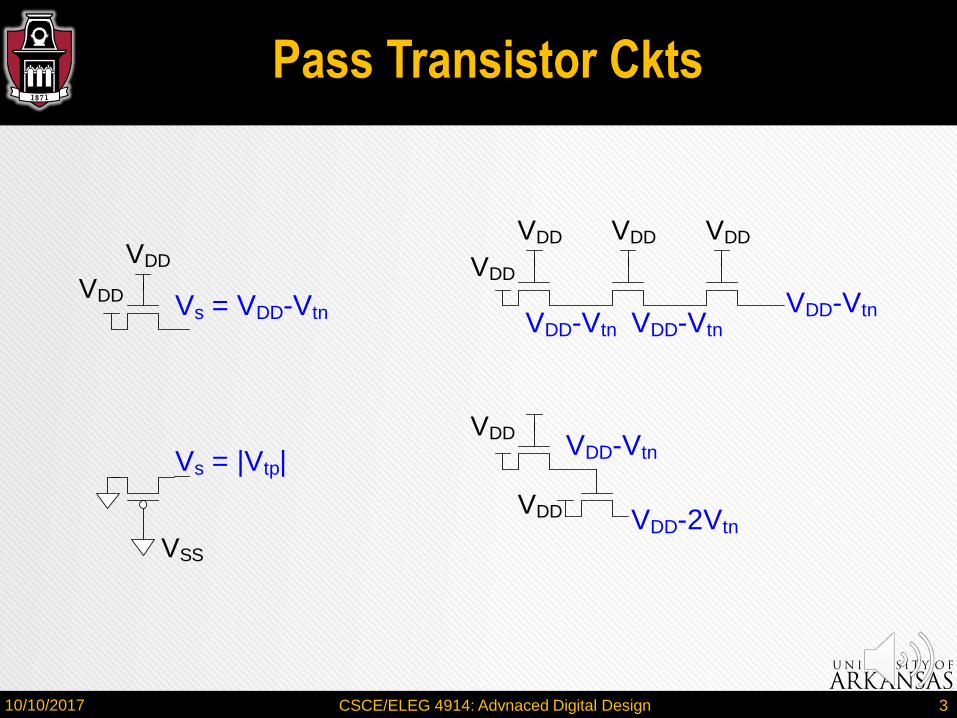
Pass Transistor Ckts
VDD
VDD
VSS
VDD
VDD
VDD VDD VDD
VDD
Vs = VDD-Vtn
Vs = |Vtp|
VDD-Vtn VDD-Vtn
VDD-Vtn
VDD-Vtn
VDD-2Vtn
10/10/2017 CSCE/ELEG 4914: Advnaced Digital Design 3
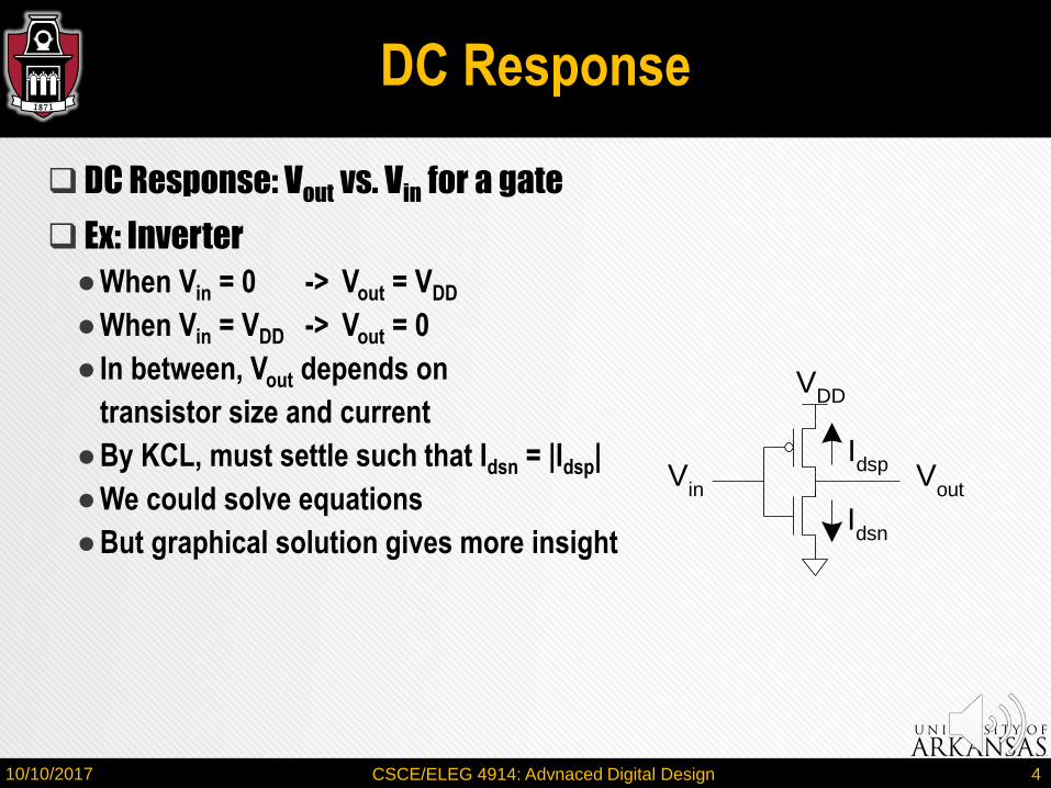
DC Response
DC Response: Vout vs. Vin for a gate
Ex: Inverter
●When Vin = 0 -> Vout = VDD
●When Vin = VDD -> Vout = 0
● In between, Vout depends on
transistor size and current
●By KCL, must settle such that Idsn = |Idsp|
●We could solve equations
●But graphical solution gives more insightIdsn
Idsp
Vout
VDD
Vin
10/10/2017 CSCE/ELEG 4914: Advnaced Digital Design 4
Transistor Operation
Current depends on region of transistor behavior
For what Vin and Vout are nMOS and pMOS in
●Cutoff?
●Linear?
●Saturation?
10/10/2017 CSCE/ELEG 4914: Advnaced Digital Design 5
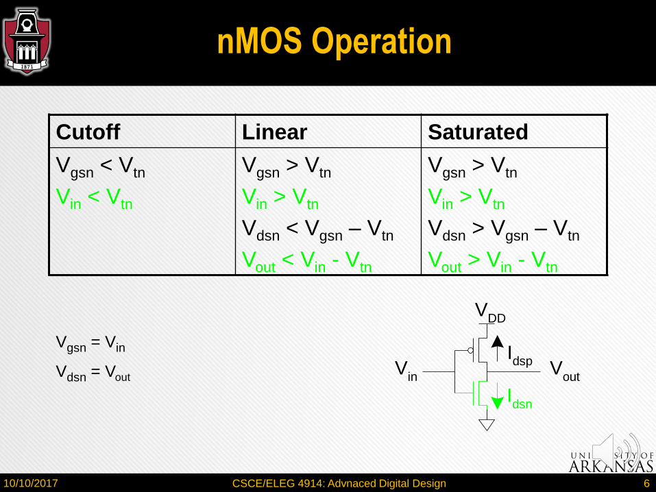
nMOS Operation
Cutoff Linear Saturated
Vgsn < Vtn
Vin < Vtn
Vgsn > Vtn
Vin > Vtn
Vdsn < Vgsn – Vtn
Vout < Vin - Vtn
Vgsn > Vtn
Vin > Vtn
Vdsn > Vgsn – Vtn
Vout > Vin - Vtn
Idsn
Idsp
Vout
VDD
Vin
Vgsn = Vin
Vdsn = Vout
10/10/2017 CSCE/ELEG 4914: Advnaced Digital Design 6
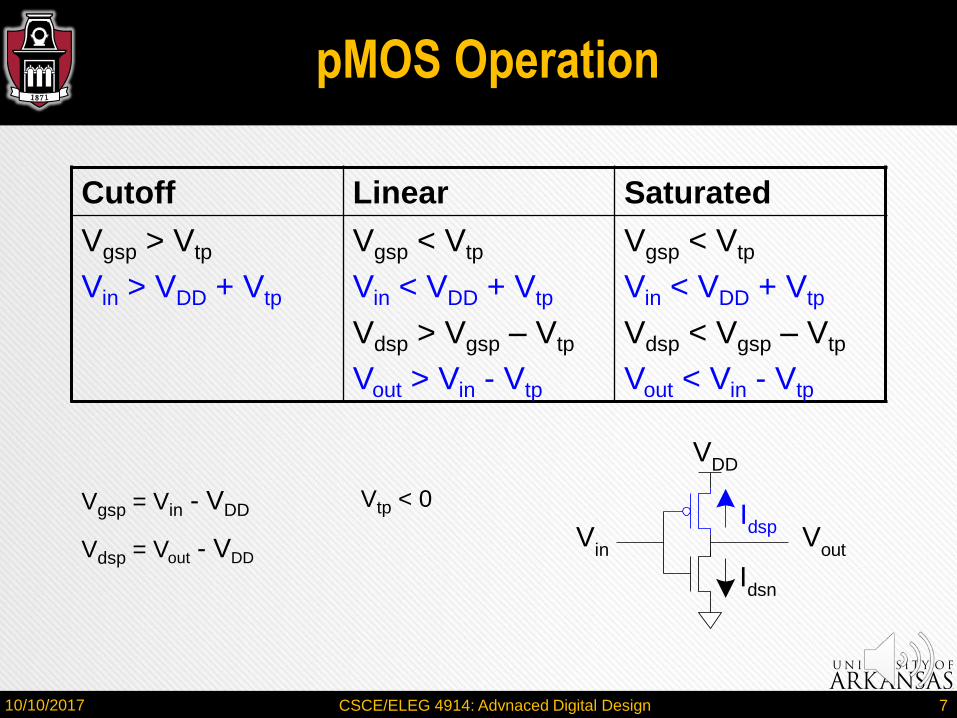
pMOS Operation
Cutoff Linear Saturated
Vgsp > Vtp
Vin > VDD + Vtp
Vgsp < Vtp
Vin < VDD + Vtp
Vdsp > Vgsp – Vtp
Vout > Vin - Vtp
Vgsp < Vtp
Vin < VDD + Vtp
Vdsp < Vgsp – Vtp
Vout < Vin - Vtp
Idsn
Idsp
Vout
VDD
Vin
Vgsp = Vin - VDD
Vdsp = Vout - VDD
Vtp < 0
10/10/2017 CSCE/ELEG 4914: Advnaced Digital Design 7
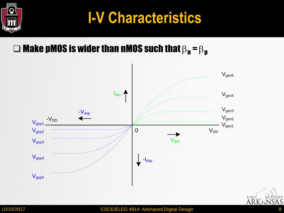
I-V Characteristics
Make pMOS is wider than nMOS such that bn = bp
Vgsn5
Vgsn4
Vgsn3
Vgsn2
Vgsn1
Vgsp5
Vgsp4
Vgsp3
Vgsp2
Vgsp1
VDD
-VDD
Vdsn
-Vdsp
-Idsp
Idsn
0
10/10/2017 CSCE/ELEG 4914: Advnaced Digital Design 8

Current vs. Vout, Vin
Vin5
Vin4
Vin3
Vin2
Vin1
Vin0
Vin1
Vin2
Vin3
Vin4
Idsn
, |Idsp
|
Vout
VDD
10/10/2017 CSCE/ELEG 4914: Advnaced Digital Design 9
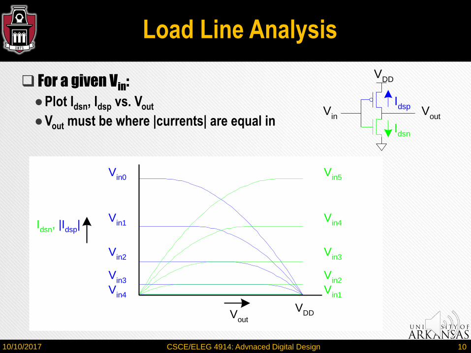
Load Line Analysis
Vin5
Vin4
Vin3
Vin2
Vin1
Vin0
Vin1
Vin2
Vin3
Vin4
Idsn
, |Idsp
|
Vout
VDD
For a given Vin:
●Plot Idsn, Idsp vs. Vout
●Vout must be where |currents| are equal inIdsn
Idsp
Vout
VDD
Vin
10/10/2017 CSCE/ELEG 4914: Advnaced Digital Design 10

Vin = 0
Load Line Analysis
Vin0
Vin0
Idsn
, |Idsp
|
Vout
VDD
10/10/2017 CSCE/ELEG 4914: Advnaced Digital Design 11
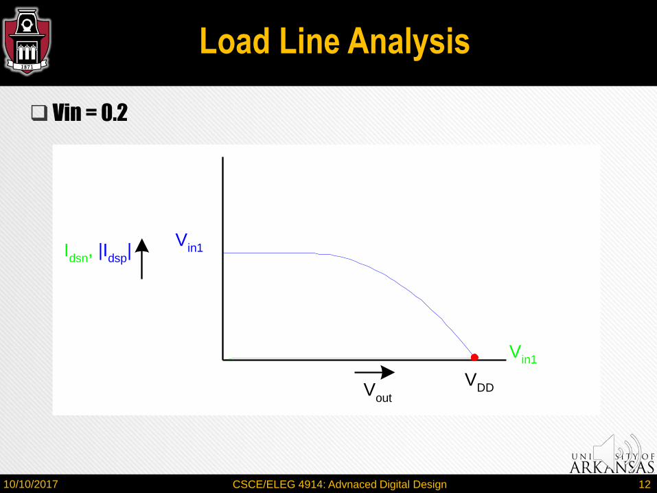
Vin = 0.2
Load Line Analysis
Vin1
Vin1I
dsn, |I
dsp|
Vout
VDD
10/10/2017 CSCE/ELEG 4914: Advnaced Digital Design 12

Vin = 0.4
Load Line Analysis
Vin2
Vin2
Idsn
, |Idsp
|
Vout
VDD
10/10/2017 CSCE/ELEG 4914: Advnaced Digital Design 13
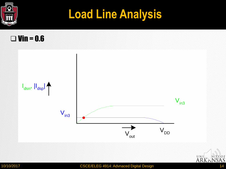
Vin = 0.6
Load Line Analysis
Vin3
Vin3
Idsn
, |Idsp
|
Vout
VDD
10/10/2017 CSCE/ELEG 4914: Advnaced Digital Design 14
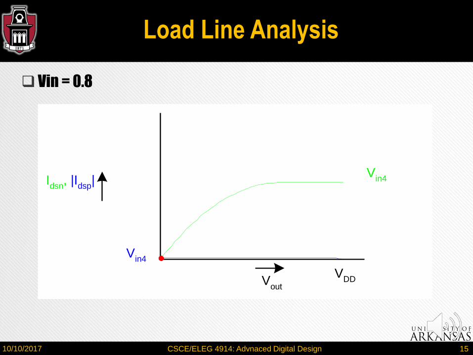
Vin = 0.8
Load Line Analysis
Vin4
Vin4
Idsn
, |Idsp
|
Vout
VDD
10/10/2017 CSCE/ELEG 4914: Advnaced Digital Design 15

Vin = 1
Load Line Analysis
Vin5
Idsn, |Idsp|
VoutVDD
10/10/2017 CSCE/ELEG 4914: Advnaced Digital Design 16
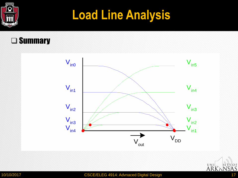
Summary
Load Line Analysis
Vin5
Vin4
Vin3
Vin2
Vin1
Vin0
Vin1
Vin2
Vin3
Vin4
Vout
VDD
10/10/2017 CSCE/ELEG 4914: Advnaced Digital Design 17
DC Transfer Curve
Transcribe points onto Vin vs. Vout plot
Transistor operating regions?
Vin5
Vin4
Vin3
Vin2
Vin1
Vin0
Vin1
Vin2
Vin3
Vin4
Vout
VDD
CV
out
0
Vin
VDD
VDD
A B
DE
Vtn
VDD
/2 VDD
+Vtp
Vin0
Vin1
Vin2
Vin3
Vin4 V
in5
10/10/2017 CSCE/ELEG 4914: Advnaced Digital Design 18
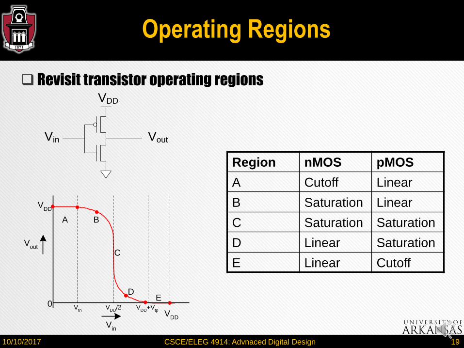
Revisit transistor operating regions
Operating Regions
Vout
VDD
Vin
CV
out
0
Vin
VDD
VDD
A B
DE
Vtn
VDD
/2 VDD
+Vtp
Region nMOS pMOS
A Cutoff Linear
B Saturation Linear
C Saturation Saturation
D Linear Saturation
E Linear Cutoff
10/10/2017 CSCE/ELEG 4914: Advnaced Digital Design 19
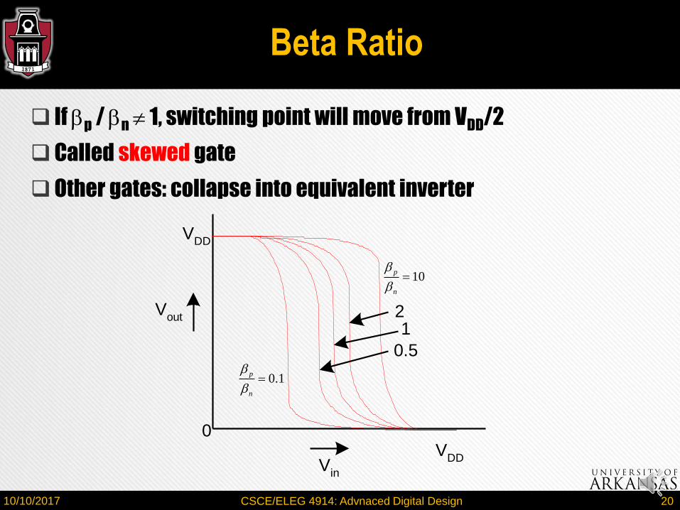
Beta Ratio
If bp / bn 1, switching point will move from VDD/2
Called skewed gate
Other gates: collapse into equivalent inverter
Vout
0
Vin
VDD
VDD
0.5
12
10p
n
b
b
0.1p
n
b
b
10/10/2017 CSCE/ELEG 4914: Advnaced Digital Design 20
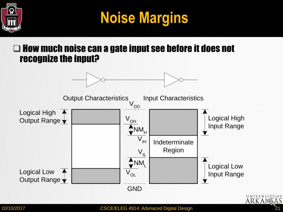
Noise Margins
How much noise can a gate input see before it does not recognize the input?
Indeterminate
Region
NML
NMH
Input CharacteristicsOutput Characteristics
VOH
VDD
VOL
GND
VIH
VIL
Logical High
Input Range
Logical Low
Input Range
Logical High
Output Range
Logical Low
Output Range
10/10/2017 CSCE/ELEG 4914: Advnaced Digital Design 21
VDD
Vin
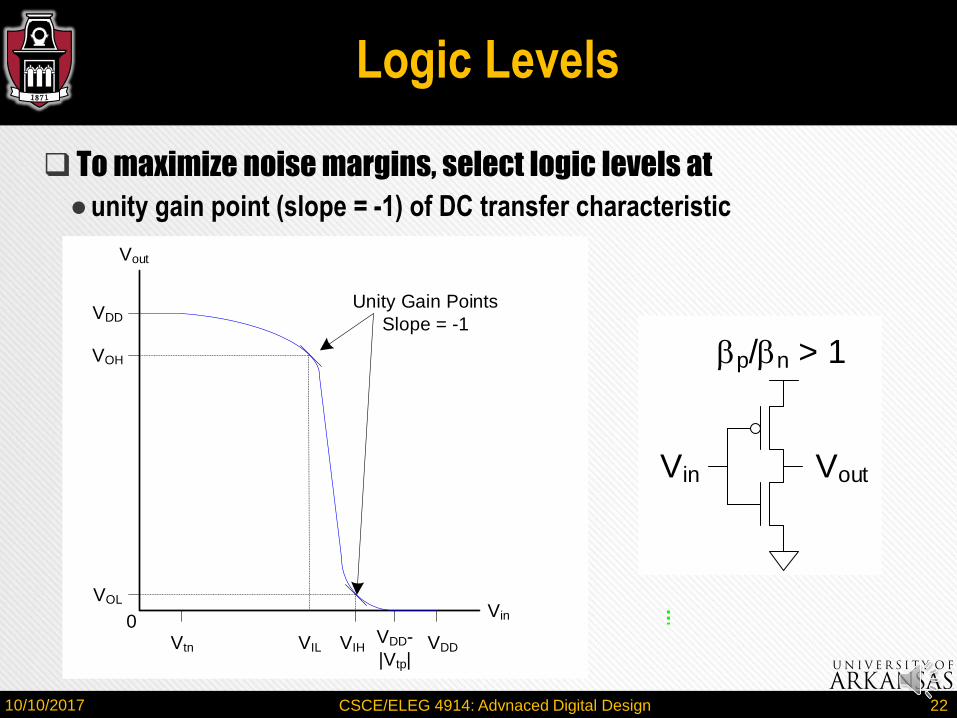
Vout
VOH
VDD
VOL
VIL VIHVtn
Unity Gain Points
Slope = -1
VDD-
|Vtp|
0
To maximize noise margins, select logic levels at
●unity gain point (slope = -1) of DC transfer characteristic
Logic Levels
bp/bn > 1
Vin Vout
10/10/2017 CSCE/ELEG 4914: Advnaced Digital Design 22
Transient Response
DC analysis tells us Vout if Vin is constant
Transient analysis tells us Vout(t) if Vin(t) changes
●Requires solving differential equations
Input is usually considered to be a step or ramp
●From 0 to VDD or vice versa
10/10/2017 CSCE/ELEG 4914: Advnaced Digital Design 23

Inverter Step Response
Ex: find step response of inverter driving load cap
0
0
( )
( )
( )
(
(
)
)
DD
DD
loa
d
ou
i
d
t
o
n
ut sn
V
V
u t t V
t t
V t
V
d
dt C
t
I t
0
2
2
0
2)
)
(( )
( DD DD t
DD
out
outout out D t
n
t
ds
D
I V
t t
V V V V
V V V VV
t
V tV t
b
b
Vout
(t)
Vin(t)
t0
t
Vin(t)
Vout
(t)C
load
Idsn
(t)
10/10/2017 CSCE/ELEG 4914: Advnaced Digital Design 24
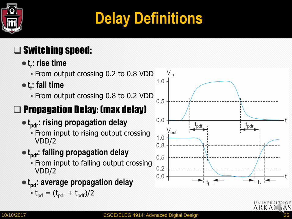
Switching speed:
● tr: rise time▪ From output crossing 0.2 to 0.8 VDD
● tf: fall time▪ From output crossing 0.8 to 0.2 VDD
Propagation Delay: (max delay)
● tpdr: rising propagation delay▪ From input to rising output crossing
VDD/2
● tpdf: falling propagation delay▪ From input to falling output crossing
VDD/2
● tpd: average propagation delay▪ tpd = (tpdr + tpdf)/2
Delay Definitions
10/10/2017 CSCE/ELEG 4914: Advnaced Digital Design 25
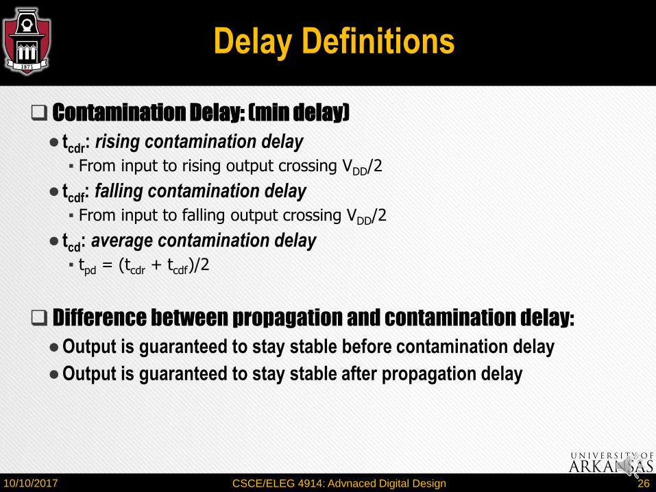
Delay Definitions
Contamination Delay: (min delay)
● tcdr: rising contamination delay▪ From input to rising output crossing VDD/2
● tcdf: falling contamination delay▪ From input to falling output crossing VDD/2
● tcd: average contamination delay▪ tpd = (tcdr + tcdf)/2
Difference between propagation and contamination delay:
●Output is guaranteed to stay stable before contamination delay
●Output is guaranteed to stay stable after propagation delay
10/10/2017 CSCE/ELEG 4914: Advnaced Digital Design 26

Simulated Inverter Delay
Solving differential equations by hand is too hard
SPICE simulator solves the equations numerically
●Uses more accurate I-V models too!
But simulations take time to write, may hide insight
(V)
0.0
0.5
1.0
1.5
2.0
t(s)0.0 200p 400p 600p 800p 1n
tpdf
= 66ps tpdr
= 83psVin
Vout
10/10/2017 CSCE/ELEG 4914: Advnaced Digital Design 27

Delay Estimation
We would like to be able to easily estimate delay
●Not as accurate as simulation
●But easier to ask “What if?”
The step response usually looks like a 1st order RC response with a decaying exponential.
Use RC delay models to estimate delay
●C = total capacitance on output node
●Use effective resistance R
●So that tpd = RC
Characterize transistors by finding their effective R
●Depends on average current as gate switches
10/10/2017 CSCE/ELEG 4914: Advnaced Digital Design 28
Effective Resistance
Shockley models have limited value
●Not accurate enough for modern transistors
●Too complicated for much hand analysis
Simplification: treat transistor as resistor
●Replace Ids(Vds, Vgs) with the effective resistance R▪ Ids = Vds/R
●R averaged across switching of a digital gate
Too inaccurate to predict current at any given time
●But good enough to predict RC delay
10/10/2017 CSCE/ELEG 4914: Advnaced Digital Design 29
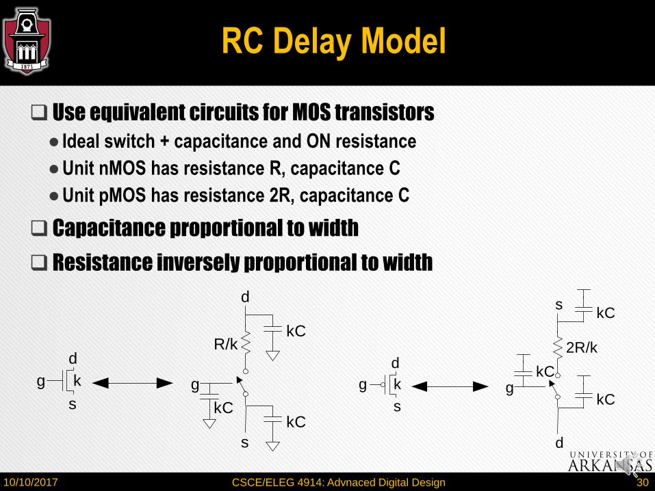
RC Delay Model
Use equivalent circuits for MOS transistors
● Ideal switch + capacitance and ON resistance
●Unit nMOS has resistance R, capacitance C
●Unit pMOS has resistance 2R, capacitance C
Capacitance proportional to width
Resistance inversely proportional to width
kg
s
d
g
s
d
kCkC
kCR/k
kg
s
d
g
s
d
kC
kC
kC
2R/k
10/10/2017 CSCE/ELEG 4914: Advnaced Digital Design 30
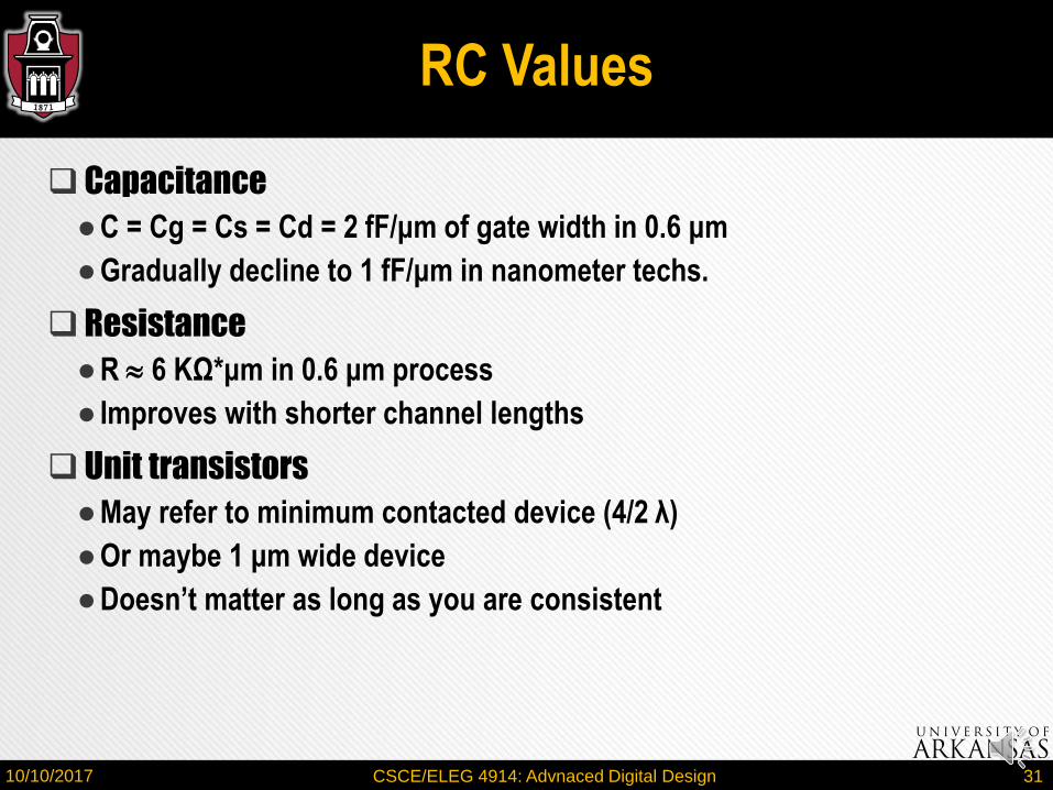
Capacitance
●C = Cg = Cs = Cd = 2 fF/μm of gate width in 0.6 μm
●Gradually decline to 1 fF/μm in nanometer techs.
Resistance
●R 6 KΩ*μm in 0.6 μm process
● Improves with shorter channel lengths
Unit transistors
●May refer to minimum contacted device (4/2 λ)
●Or maybe 1 μm wide device
●Doesn’t matter as long as you are consistent
RC Values
10/10/2017 CSCE/ELEG 4914: Advnaced Digital Design 31
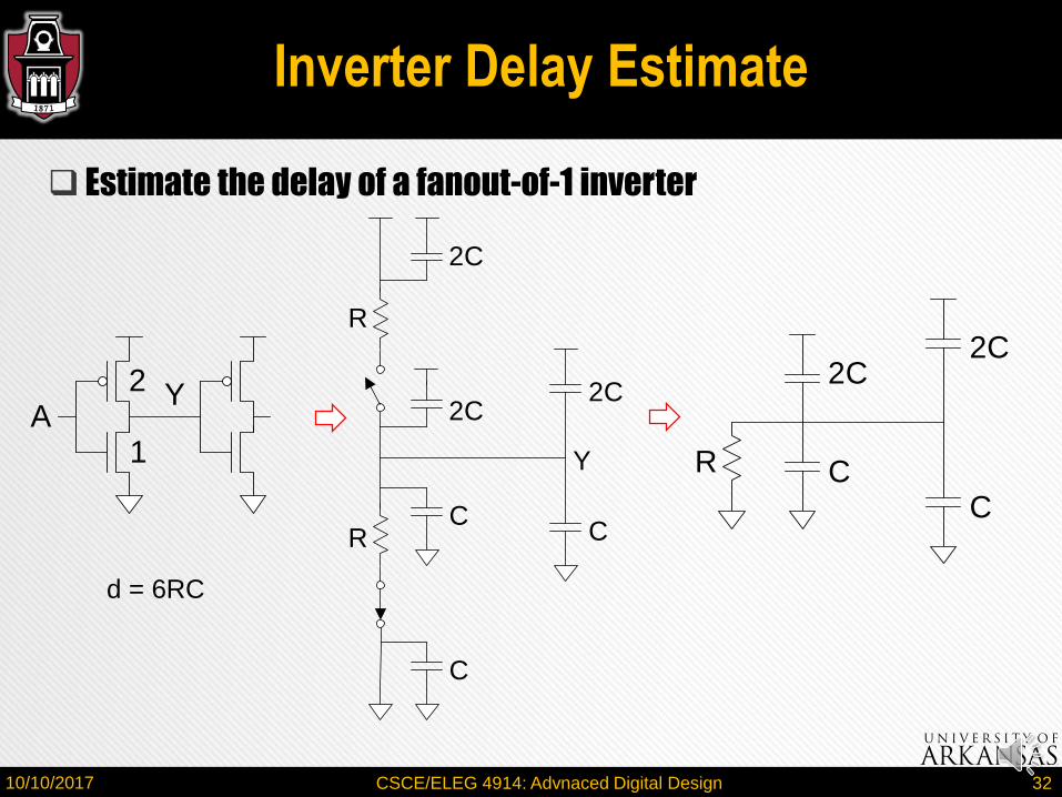
Inverter Delay Estimate
Estimate the delay of a fanout-of-1 inverter
d = 6RC
2
1A
Y
C
CR
2C
2C
R
C
2C
Y C
2C
C
2C
R
10/10/2017 CSCE/ELEG 4914: Advnaced Digital Design 32

Delay Model Comparison
10/10/2017 CSCE/ELEG 4914: Advnaced Digital Design 33
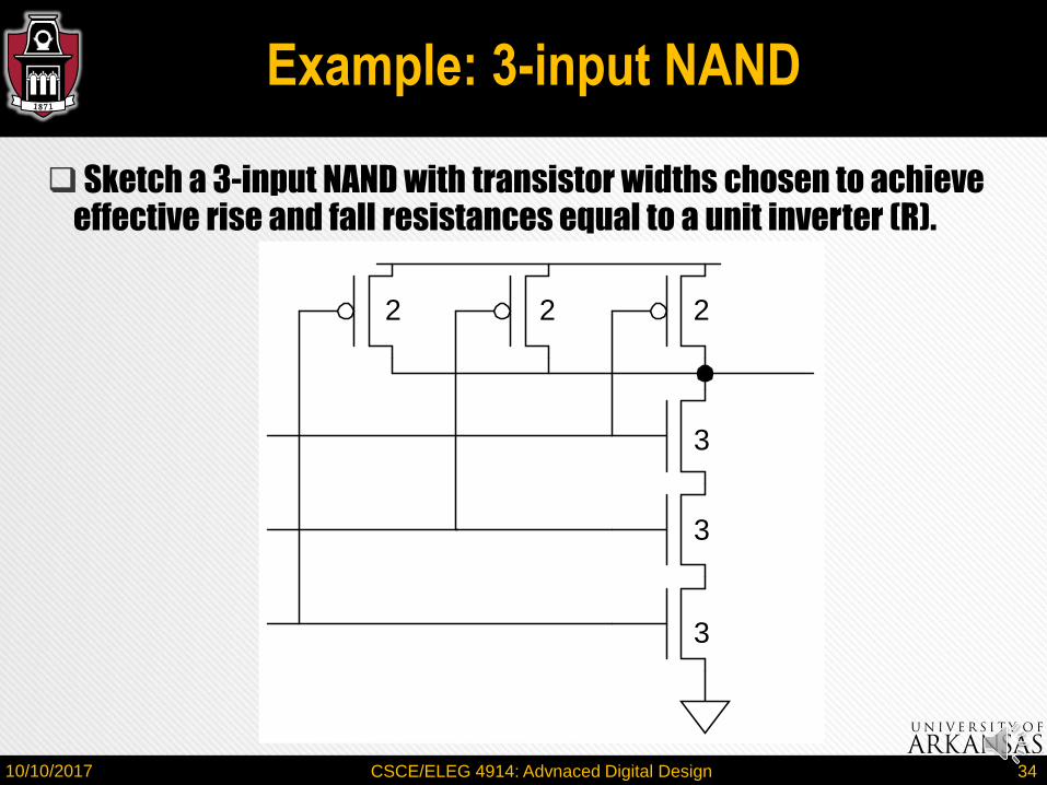
Sketch a 3-input NAND with transistor widths chosen to achieve effective rise and fall resistances equal to a unit inverter (R).
Example: 3-input NAND
3
3
3
2 2 2
10/10/2017 CSCE/ELEG 4914: Advnaced Digital Design 34
2 2 2
3
3
3
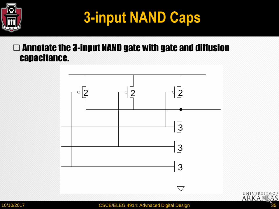
Annotate the 3-input NAND gate with gate and diffusion capacitance.
3-input NAND Caps
10/10/2017 CSCE/ELEG 4914: Advnaced Digital Design 35
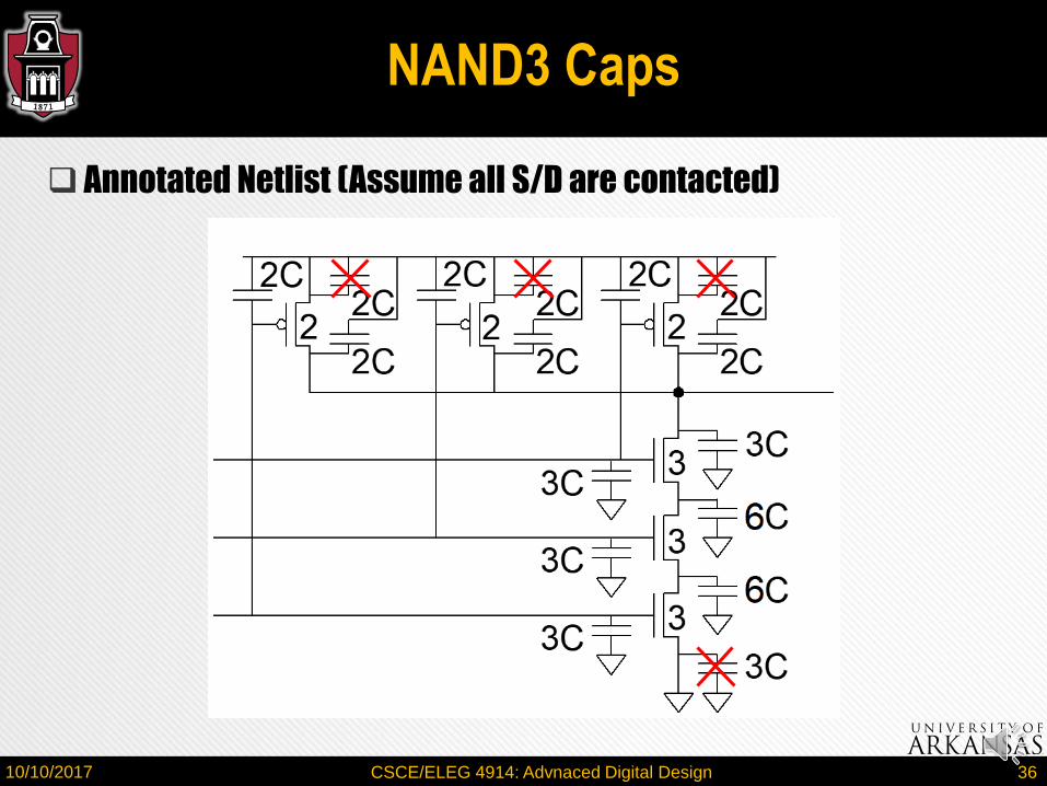
Annotated Netlist (Assume all S/D are contacted)
NAND3 Caps
10/10/2017 CSCE/ELEG 4914: Advnaced Digital Design 36
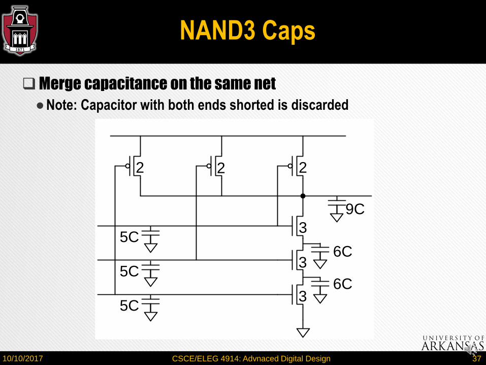
Merge capacitance on the same net
●Note: Capacitor with both ends shorted is discarded
NAND3 Caps
2 2 2
3
3
36C
6C
5C
5C
5C
9C
10/10/2017 CSCE/ELEG 4914: Advnaced Digital Design 37
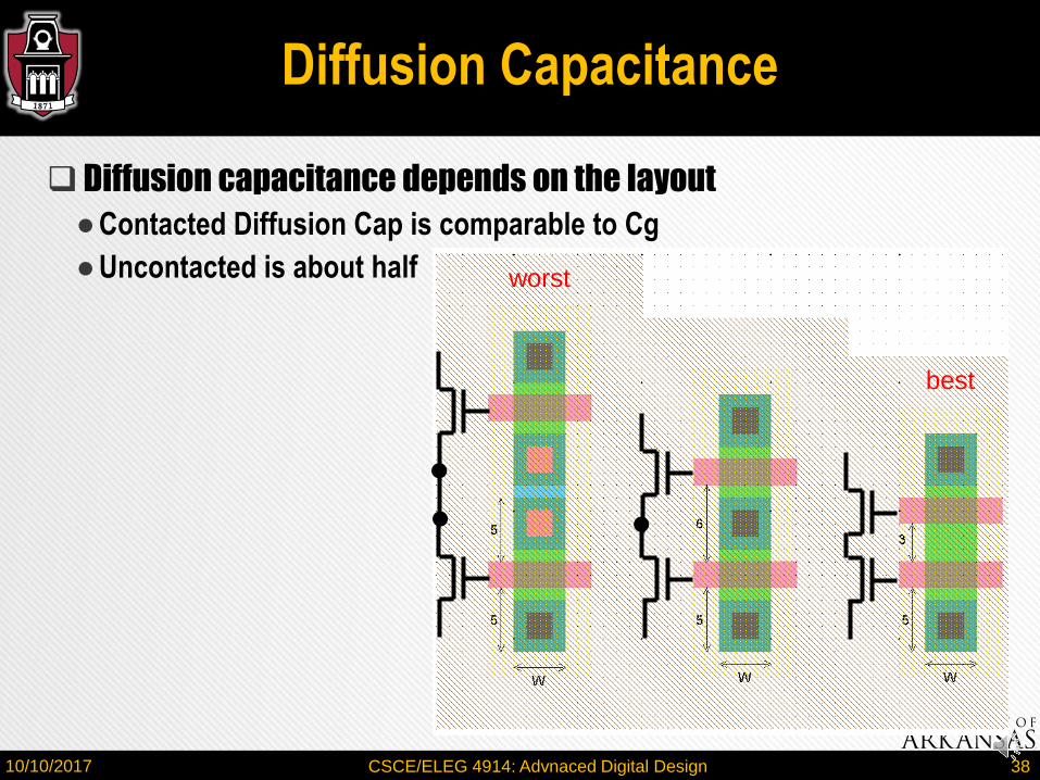
best
worst
Diffusion capacitance depends on the layout
●Contacted Diffusion Cap is comparable to Cg
●Uncontacted is about half
Diffusion Capacitance
10/10/2017 CSCE/ELEG 4914: Advnaced Digital Design 38
2C
2C
2C
2C
2C
2C2C 2C 2C
3C
3C
3C
3C3C
3C
3C
2 2 2
3
3
3
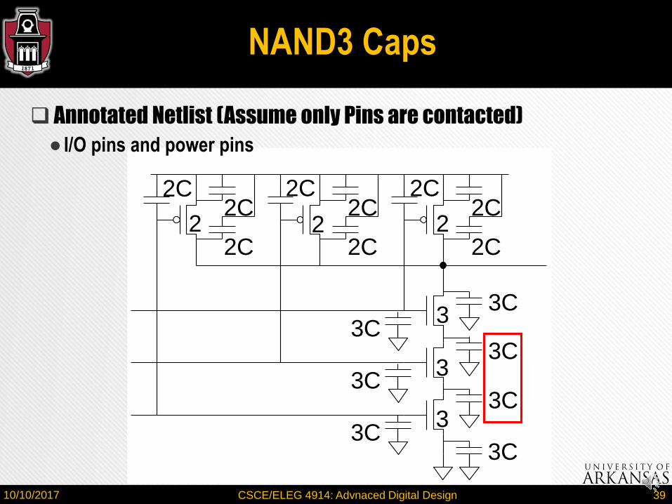
Annotated Netlist (Assume only Pins are contacted)
● I/O pins and power pins
NAND3 Caps
10/10/2017 CSCE/ELEG 4914: Advnaced Digital Design 39
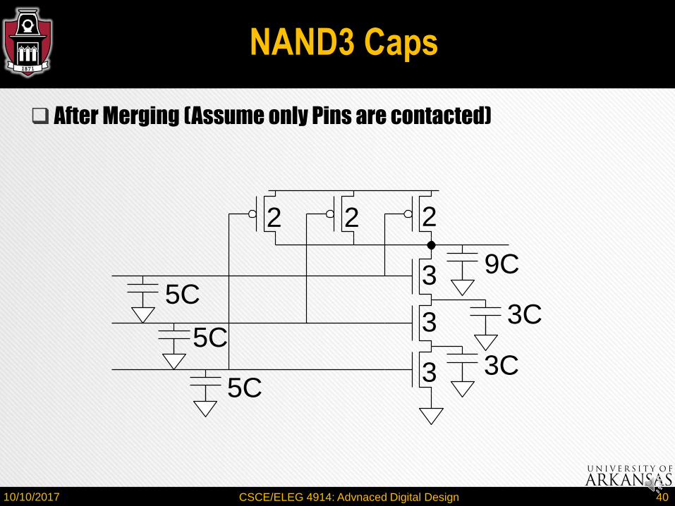
After Merging (Assume only Pins are contacted)
NAND3 Caps
9C
3C
3C3
3
3
222
5C
5C
5C
10/10/2017 CSCE/ELEG 4914: Advnaced Digital Design 40
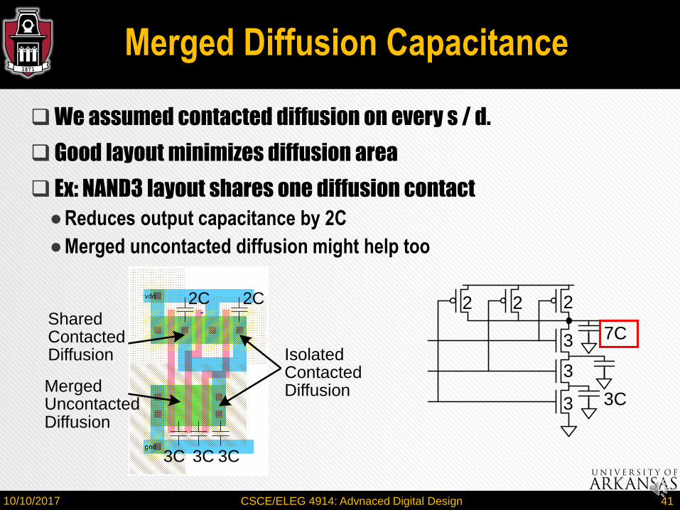
We assumed contacted diffusion on every s / d.
Good layout minimizes diffusion area
Ex: NAND3 layout shares one diffusion contact
●Reduces output capacitance by 2C
●Merged uncontacted diffusion might help too
Merged Diffusion Capacitance
7C
3C3
3
3
222
3C
2C2C
3C3C
IsolatedContactedDiffusionMerged
UncontactedDiffusion
SharedContactedDiffusion
10/10/2017 CSCE/ELEG 4914: Advnaced Digital Design 41
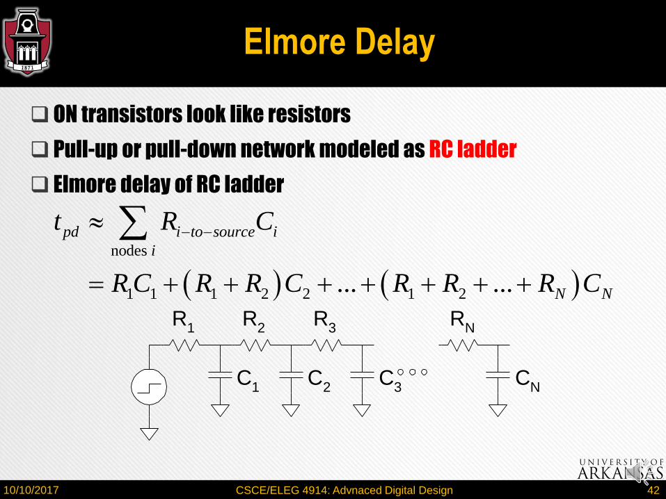
Elmore Delay
ON transistors look like resistors
Pull-up or pull-down network modeled as RC ladder
Elmore delay of RC ladder
R1
R2
R3
RN
C1
C2
C3
CN
nodes
1 1 1 2 2 1 2... ...
pd i to source i
i
N N
t R C
R C R R C R R R C
10/10/2017 CSCE/ELEG 4914: Advnaced Digital Design 42

Estimate worst-case rising and falling delay of 3-input NAND driving h identical gates.
Example: NAND3
9C
3C
3C3
3
3
222
5hC
Y
n2
n1h copies
9 5pdrt h RC
10/10/2017 CSCE/ELEG 4914: Advnaced Digital Design 43
3 3 3 3 3 33 3 9 5
11 5
R R R R R Rpdft C C h C
h RC
+ (3C)(R+R/3) + (3C) (R+R/3+R/3)= (18+5h)RC
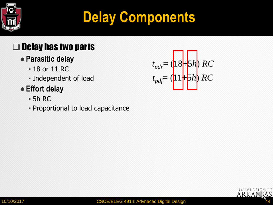
Delay has two parts
●Parasitic delay▪ 18 or 11 RC
▪ Independent of load
●Effort delay▪ 5h RC
▪ Proportional to load capacitance
Delay Components
10/10/2017 CSCE/ELEG 4914: Advnaced Digital Design 44
tpdr= (18+5h) RC
tpdf= (11+5h) RC
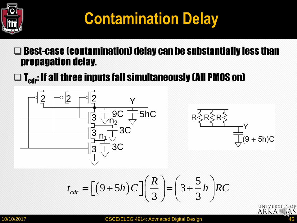
Best-case (contamination) delay can be substantially less than propagation delay.
Tcdr: If all three inputs fall simultaneously (All PMOS on)
Contamination Delay
9C
3C
3C3
3
3
222
5hC
Y
n2
n1
5
9 5 33 3
cdr
Rt h C h RC
10/10/2017 CSCE/ELEG 4914: Advnaced Digital Design 45
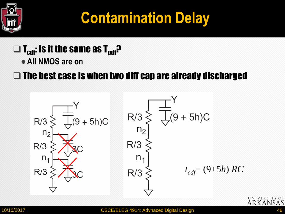
Tcdf: Is it the same as Tpdf?
●All NMOS are on
The best case is when two diff cap are already discharged
Contamination Delay
10/10/2017 CSCE/ELEG 4914: Advnaced Digital Design 46
tcdf= (9+5h) RC
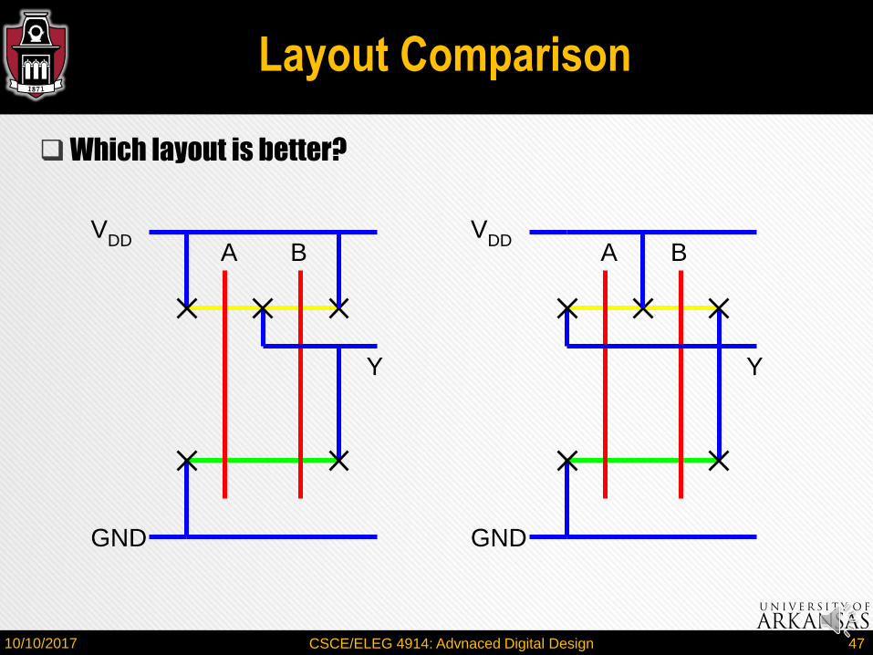
Layout Comparison
Which layout is better?
AV
DD
GND
B
Y
AV
DD
GND
B
Y
10/10/2017 CSCE/ELEG 4914: Advnaced Digital Design 47