coldfire® dsp hands-on workshop...
TRANSCRIPT

© Freescale Semiconductor, Inc., 2007. All rights reserved.
TM
COLDFIRE® DSP HANDS-ON
WORKSHOP MANUAL
ColdFire® DSP Hands-On Workshop Manual
Freescale Semiconductor 2
Introduction: The scope of these experiments have been designed to familiarize and
educate the attendees on the signal processing capabilities of the M5222x ColdFire
class
of microprocessors, with an embedded Multiply and Accumulate (MAC) unit. The
demonstrations are limited to simple examples on the effects of sampling and filter
implementations of Infinite Impulse Response (IIR) filters of different types.
The experiments are designed to enable students realize experimentally some of the
digital signal processing concepts that had been taught during the lecture.
Hardware: Mechanical resonator, sensor, ColdFire
evaluation board, laptop and impact
hammer.
Note: If you do not have the mechanical resonator and sensor, you can still do the lab
with just the ColdFire board. See Appendix for details.
Software: Freescale CodeWarrior 6.4 and LabVIEW
graphic display.
Experiments
1. Digital filter Demo: Low Pass and High Pass Filter Demonstration
WALK-IN DEMO !!
Introduction: The scope of this experiment is to generate a signal sampled at
3030 Hz, pass it through a 4th
order low pass filter (fc= 120 Hz) and 4th
order high
pass filter (fc= 350 Hz), respectively. The effects of filtering should be evident on
the displayed signals. Also, the computational efficiency, in terms of processor
cycles should be emphasized
Procedure:
a. Strike the beam with the metal impact hammer provided.
b. Stop the display when the signal is in full view
c. Zoom on a section of each plot
Observation:
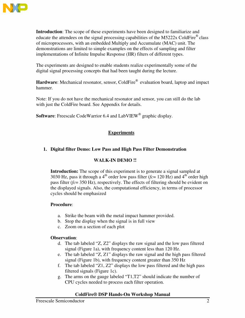
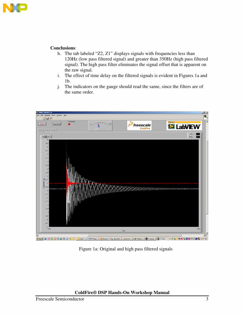
d. The tab labeled “Z, Z2” displays the raw signal and the low pass filtered
signal (Figure 1a), with frequency content less than 120 Hz.
e. The tab labeled “Z, Z1” displays the raw signal and the high pass filtered
signal (Figure 1b), with frequency content greater than 350 Hz
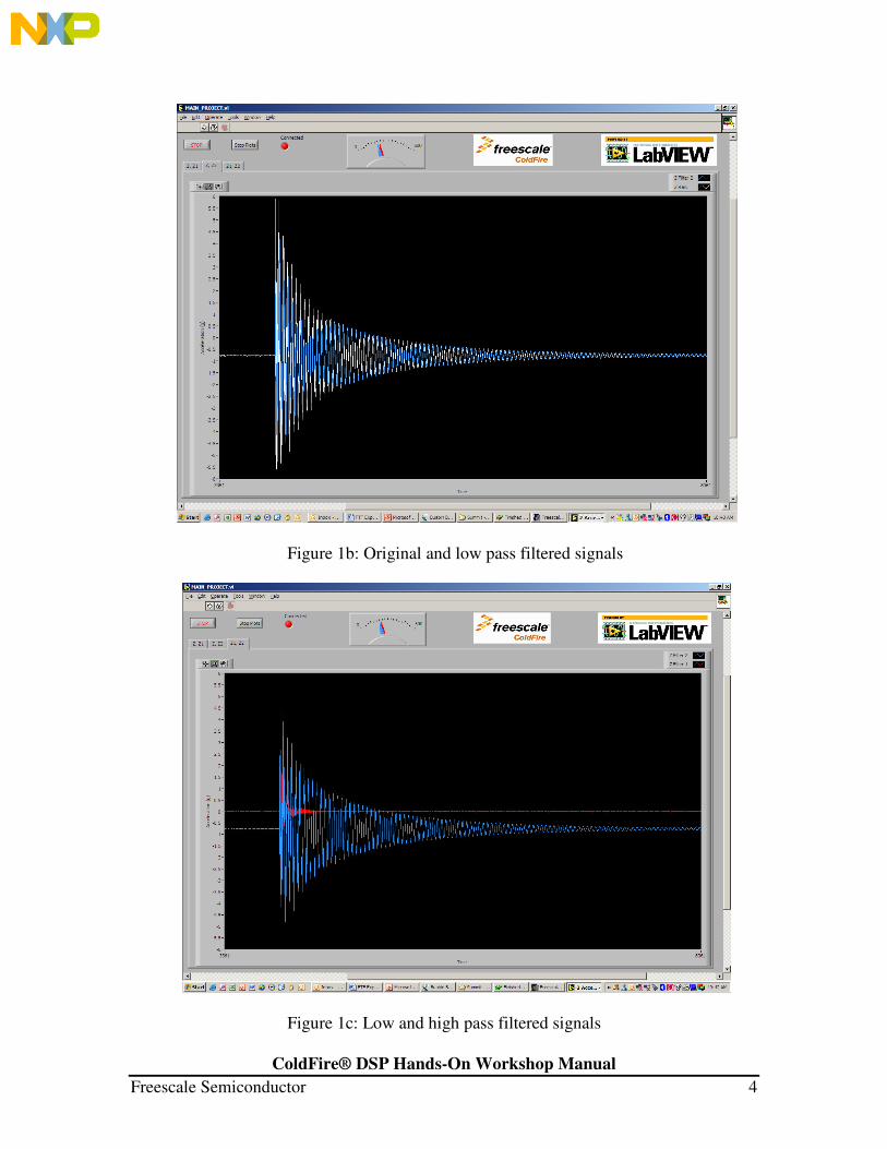
f. The tab labeled “Z1, Z2” displays the low pass filtered and the high pass
filtered signals (Figure 1c).
g. The arms on the gauge labeled “T1,T2” should indicate the number of
CPU cycles needed to process each filter operation.
ColdFire® DSP Hands-On Workshop Manual
Freescale Semiconductor 3
Conclusions:
h. The tab labeled “Z2, Z1” displays signals with frequencies less than
120Hz (low pass filtered signal) and greater than 350Hz (high pass filtered
signal). The high pass filter eliminates the signal offset that is apparent on
the raw signal.
i. The effect of time delay on the filtered signals is evident in Figures 1a and
1b.
j. The indicators on the gauge should read the same, since the filters are of
the same order.
Figure 1a: Original and high pass filtered signals
ColdFire® DSP Hands-On Workshop Manual
Freescale Semiconductor 4
Figure 1b: Original and low pass filtered signals
Figure 1c: Low and high pass filtered signals

ColdFire® DSP Hands-On Workshop Manual
Freescale Semiconductor 5
2. Digital filter design: High Pass Digital Filter Design
Introduction: The scope of this experiment is to generate a signal sampled at
3030 Hz, pass the measured signal through two high pass filters. The filters will
be designed during the course of the experiment. The selected filters should be of
the same order but different cut off frequencies. The effects of filter cut-off
frequencies on filter performance should be evident on each filtered signal.
Procedure:
a. Scroll to the subheading “EXPERIMENT 2”, in the file
hands_on_lab_exercises.c.
b. Select a 4th
order high pass filter with a cut-off frequency (fc) of 350Hz on
channel Z2 (data path 2) and a high pass 4th
order filter with cutoff
frequency of 900Hz on channel Z1 (data path 1). The filter selection
process is explained in the “Software Initialization Procedure”.
c. Perform “Software Initialization Procedure” as stated in the appendix.
d. The default sampling frequency is set to 3kHz
e. Strike the beam with the impact hammer and stop the display when the
generated signal is in full view.
Observation:
f. The tab labeled “Z, Z1” displays the raw signal and the high pass filtered
signal (Figure 2a), with frequency content greater than 900 Hz.
g. The tab labeled “Z, Z2” displays the raw signal and the high pass filtered
signal (Figure 2b), with frequency content greater than 350 Hz.
h. The tab labeled “Z1, Z2” displays the both high pass filtered signals
(Figure 2c).
i. The gauge labeled “T1,T2” is an indication of the number of CPU cycles
needed to process each filter operation
Conclusions:
j. The tab labeled “Z1, Z2” displays two signals, with frequencies higher
than 900Hz and 350Hz, respectively. The high pass filters eliminate the
signal offset that is apparent on the raw signal.
k. The effect of time delay on the filtered signals is evident in Figures 2a and
2b.
l. The indicators on the gauge should read the same for both signals, since
the amount of CPU cycle is proportional to the filter order.

ColdFire® DSP Hands-On Workshop Manual
Freescale Semiconductor 6
Figure 2a: Measured and High pass filtered signals (fc=900 Hz)
Figure 2b: Measured and high pass filtered signals (fc=350Hz)

ColdFire® DSP Hands-On Workshop Manual
Freescale Semiconductor 7
Figure 2c: High pass filtered signals with cut off frequency at 900 Hz and 350Hz
3. Digital filter design: Cascaded Filter design
Introduction: The scope of this experiment is to generate a signal sampled at
3030 Hz, pass it through 4th
order, low pass filter (fc=350Hz) cascaded to a 3rd
order, high pass filter (fc=100Hz). The signal from the cascaded channel is
compared to the filtered signal from a 4th
order, band pass filter (fc=350Hz). The
comparative effects of filtering on signal frequency content, time delay, processor
cycle count and elimination of low frequency offset, should be evident.
Procedure:
a. Scroll to the heading “Timer Settings” in the file
hands_on_lab_exercises.c
b. Scroll up to the heading “CASCADED FITLER DESIGN:
EXPERIMENT 4”, delete the first set of block comments”/*” and “*/”.
c. This automatically selects the filters for the cascade filer design
experiment.

ColdFire® DSP Hands-On Workshop Manual
Freescale Semiconductor 8
d. Look for the subheading “data path 1: CASCADED FILTERS” and
uncomment the line of code “iir(&filter0)”under this subheading, as
explained in step 7 of the “Software initialization procedure”.
e. Deselect all the filters in subheading “NON-CASCADED FILTER
DESIGN” as explained in step 7 of the “Software initialization
procedure”.
f. Set sampling frequency to 3030 Hz by initializing the variable
“sample_rate_reduction_log2” to the value 0, in the file
“hands_on_lab_exercises.c”. This divides the base ADC sampling rate of
3030 kHz by a factor of 20, or 1.
g. Repeat Software Initialization Procedure, starting at step 8.
h. Strike beam with the impact hammer and stop the display when the
generated signal is in full view.
i. Zoom on an area of the plot to demonstrate the presence of selected
frequency bands on the filtered signal.
Observation:
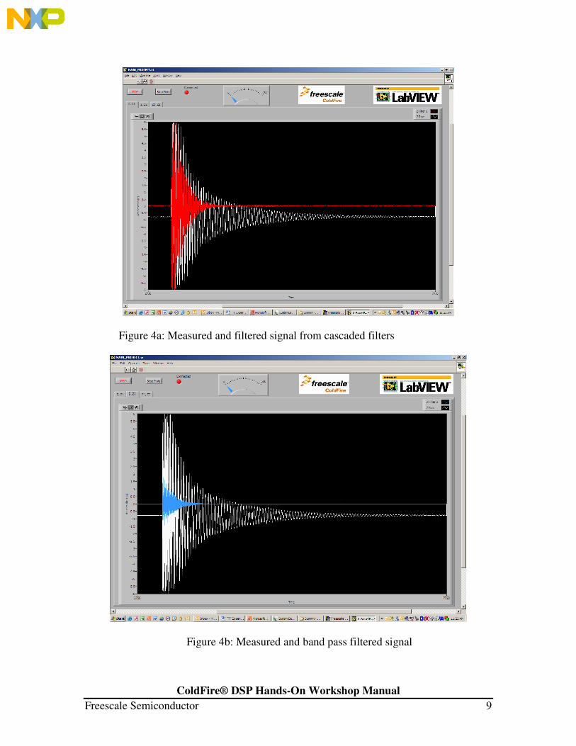
j. The tab labeled “Z, Z1” displays the raw signal and the signal at the output
of the cascaded filters (Figure 4a).
k. The tab labeled “Z, Z2” displays the raw signal and the band pass filtered
signal (Figure 4b).
l. The tab labeled “Z1, Z2” displays the band pass filtered signal and the
signal at the output of the cascaded filters (Figure 4c).
m. The gauge labeled “T1,T2” is an indication of the number of CPU cycles
needed to process each filter operation
Conclusions:
n. The tab labeled “Z1, Z2” displays signals with frequencies more than
100Hz (high pass filtered signal) and less than 120Hz (low pass filtered
signal). The high pass and the band pass filters eliminate the signal offset
that is apparent on the raw signal.
o. The effect of time delay on the filtered signals is evident in Figures 4a, 4b
and 4c.
p. The indicators on the gauge should read higher for the cascaded filters,
since the amount of CPU cycle is proportional to the filter order.
ColdFire® DSP Hands-On Workshop Manual
Freescale Semiconductor 9
Figure 4a: Measured and filtered signal from cascaded filters
Figure 4b: Measured and band pass filtered signal
ColdFire® DSP Hands-On Workshop Manual
Freescale Semiconductor 10
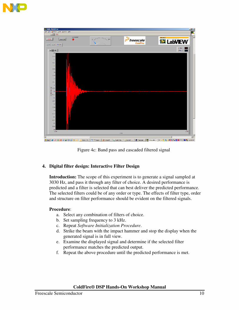
Figure 4c: Band pass and cascaded filtered signal
4. Digital filter design: Interactive Filter Design
Introduction: The scope of this experiment is to generate a signal sampled at
3030 Hz, and pass it through any filter of choice. A desired performance is
predicted and a filter is selected that can best deliver the predicted performance.
The selected filters could be of any order or type. The effects of filter type, order
and structure on filter performance should be evident on the filtered signals.
Procedure:
a. Select any combination of filters of choice.
b. Set sampling frequency to 3 kHz.
c. Repeat Software Initialization Procedure.
d. Strike the beam with the impact hammer and stop the display when the
generated signal is in full view.
e. Examine the displayed signal and determine if the selected filter
performance matches the predicted output.
f. Repeat the above procedure until the predicted performance is met.

ColdFire® DSP Hands-On Workshop Manual
Freescale Semiconductor 11
5. Signal Aliasing
Introduction: The scope of this experiment is to generate a signal that is sampled
at a frequency lower than the base sampling rate of 3030 Hz. The effects of time
domain aliasing should be evident on the displayed signals.
Procedure:
a. Set sampling frequency to 758 Hz by initializing the variable
“sample_rate_reduction_log2” to the value 2, in the file
“hands_on_lab_exercises.c”. This divides the base ADC sampling rate of
3030 kHz by a factor of 22, or 4.
b. Perform the software Initialization procedure, starting at step 6.
c. Strike beam with the impact hammer and stop the display when the
generated signal is in full view.
d. Zoom on an area of the displayed signals
Observation:
e. The tab labeled “Z, Z1” displays the raw signal and the low pass filtered
signal (Figure 2a).
f. The tab labeled “Z, Z2” displays the raw signal and the High pass filtered
signal (Figure 2b).
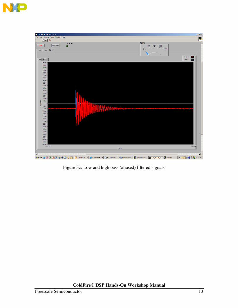
g. The tab labeled “Z1, Z2” displays the low pass filtered and the high pass
filtered signals (Figure 2c).
Conclusions:
h. The tab labeled “Z1, Z2” displays signals with frequencies less than
120Hz (low pass filtered signal) and greater than 900Hz (high pass filtered
signal). The high pass filter eliminates the signal offset that is apparent on
the raw signal.
i. The effects of signal aliasing are evident on a zoomed view of each
display. The raw and high passed filtered signals have been aliased. The
signals seem to be of the same frequency as the low pass filtered signal
and the jagged signal peaks on the raw and high pass filtered signals are
characteristic of aliased signals. Hence signal have been aliased to
frequencies below the Nyquist frequency, f_nyq=376 Hz.
j. The effect of time delay on the filtered signals is evident in Figures 3a and
3b.
k. The indicators on the gauge should read higher for the 5th
order filtered
signal, since the amount of CPU cycle is proportional to the filter order.
ColdFire® DSP Hands-On Workshop Manual
Freescale Semiconductor 12
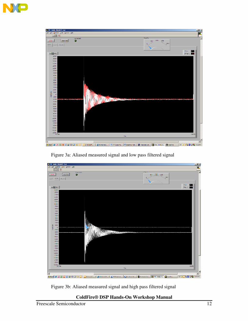
Figure 3a: Aliased measured signal and low pass filtered signal
Figure 3b: Aliased measured signal and high pass filtered signal
ColdFire® DSP Hands-On Workshop Manual
Freescale Semiconductor 13
Figure 3c: Low and high pass (aliased) filtered signals

ColdFire® DSP Hands-On Workshop Manual
Freescale Semiconductor 14
APPENDIX
Software Initialization Procedure: Repeat this procedure as necessary.
1) Close LabVIEW
2) Launch CodeWarrior version 6.4 from your desktop
3) Open the project dsp_library_project.mcp, select target m5222x_Ruler_demo
and open the file “hands_on_lab_exercises.c”. If you do not have the mechanical
resonator, you can use the accelerometer mounted on the ColdFire board. In this
case, use target m5222x_demo_flash or m5221x_demo_flash depending on
which board you have.
4) Scroll to the sub heading “Filter design Experiments”.
5) For Non-cascaded filter design, scroll to the subheading, “Non-Cascaded Filter
Design” and select a filter in each of the subgroups “data path 1” and “data path
2”, respectively.
6) For cascaded filter design, scroll to the subheading, “Cascaded Filter Design”,
select 2 filters in the “data path 1” subgroup and a filter in the “data path 2”
subgroup.
7) Select a desired filter by deleting the characters “//” preceding the function
“iir_init”. This should uncomment the text, which will be highlighted in blue.
This means the filter has been selected and is active in the data path. Effectively,
this procedure changes the filter coefficients.
8) Deselect a filter by typing the characters “//” preceding the function “iir_init”.
This should comment the text, which will be highlighted in red. This means the
filter has been deselected and is inactive in the data path.
9) Save the file (Ctrl S) and Make (F7) the code.
10) Select “Flash Programmer” from the tools menu and highlight the “target
configuration” option in the menu page on the left. Then click on the “load
settings” button and select “CFM_MCF52221.xml” in the ColdFire
folder, and
click Open. (The complete path is C:\Program Files\CodeWarrior for ColdFire
V6.4\bin\Plugins\Support\Flash_Programmer\ColdFire)
11) Select the “Erase/ blank check” option in the menu page, and click the “Erase”
tab. This erases the current software on the board.
12) When the status bar reads “Erase command succeeded”, select the “Program
/Verify” option on the menu page and select the “Program” tab to download
software to the board.
13) When the status bar reads “Program command Succeeded”, click “OK” and the
board is now programmed with software containing resent changes.
14) Run the code on the board by clicking the Run button (green play arrow) or
cycling the power switch to the board
15) Launch LabVIEW from the desktop and maximize the screen
16) The system defaults to the START simulation state.
17) When the system starts running, STOP the display and START it again. This
should display captured data on the screen. If not, STOP the display, cycle power
to the board and START the display again.
ColdFire® DSP Hands-On Workshop Manual
Freescale Semiconductor 15
18) NOTE: This step may need to be repeated as often as necessary to initialize the
COM port and get data streaming to the display.
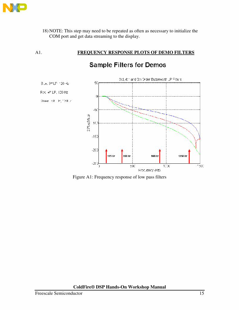
A1. FREQUENCY RESPONSE PLOTS OF DEMO FILTERS
Figure A1: Frequency response of low pass filters

ColdFire® DSP Hands-On Workshop Manual
Freescale Semiconductor 16
Figure A2: Frequency response of high and low pass filters
Figure A3: Frequency response of high pass filters
ColdFire® DSP Hands-On Workshop Manual
Freescale Semiconductor 17
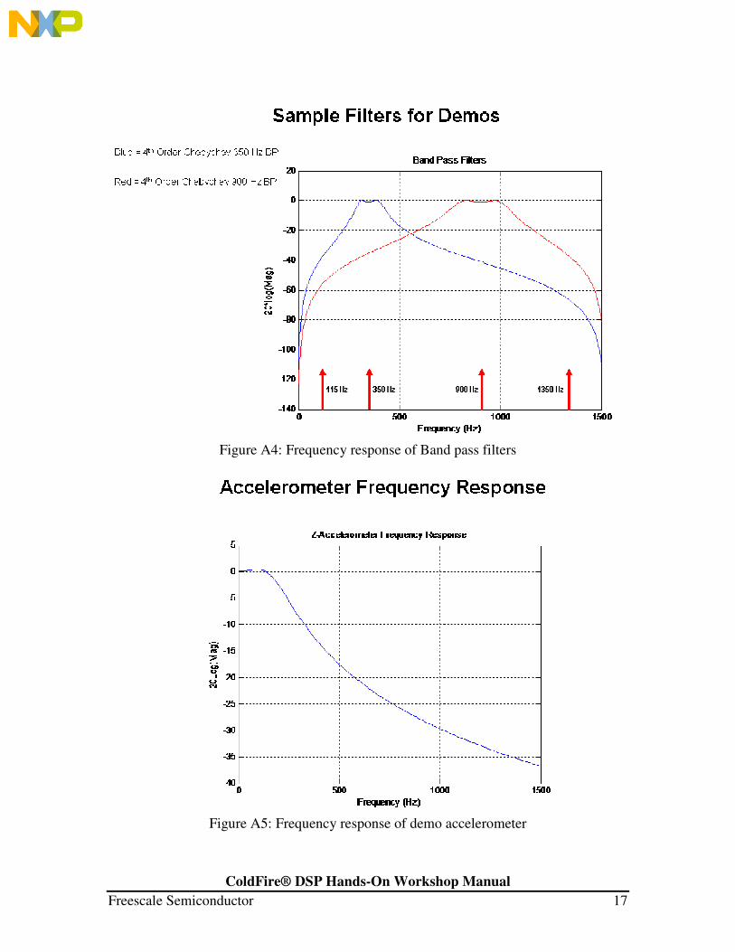
Figure A4: Frequency response of Band pass filters
Figure A5: Frequency response of demo accelerometer