mcr20a 2.4 ghz low-power transceiver reference...
TRANSCRIPT
MCR20A 2.4 GHz Low-PowerTransceiver Reference Manual
Supports: MCR20AVHM
Document Number: MCR20ARMRev. 3, July 2016

MCR20A 2.4 GHz Low-Power Transceiver Reference Manual, Rev. 3, July 2016
2 NXP Semiconductors
Contents
Section number Title Page
Chapter 1Introduction to MCR20A
1.1 Introduction.....................................................................................................................................................................13
1.2 Block Diagram................................................................................................................................................................14
1.3 Modem Features Summary.............................................................................................................................................15
1.4 RF Interface and Usage...................................................................................................................................................17
1.5 Radio Architecture.......................................................................................................................................................... 17
1.5.1 Packet Structure................................................................................................................................................. 17
1.5.2 Receive Path Description................................................................................................................................... 17
1.5.3 Transmit Path Description................................................................................................................................. 18
1.6 IEEE 802.15.4 Acceleration Hardware...........................................................................................................................18
1.7 Advanced Security Module (ASM) Overview............................................................................................................... 19
1.8 MCU Interface with SPI Overview.................................................................................................................................20
1.8.1 Transceiver Control Overview...........................................................................................................................21
1.9 Clock Output, RF Control, and GPIO Summary............................................................................................................ 22
1.9.1 CLK_OUT Reference........................................................................................................................................ 22
1.9.2 RF Control Signals.............................................................................................................................................22
1.9.3 Antenna Diversity.............................................................................................................................................. 23
1.9.4 General Purpose Input Output (GPIO)...............................................................................................................23
1.10 Modem Operational Modes............................................................................................................................................ 23
1.11 External PA and LNA.....................................................................................................................................................24
Chapter 2Signal Multiplexing and Signal Descriptions
2.1 Pin assignments...............................................................................................................................................................25
2.2 Pin function table............................................................................................................................................................ 26
Chapter 3System Considerations
3.1 Introduction.....................................................................................................................................................................29
MCR20A 2.4 GHz Low-Power Transceiver Reference Manual, Rev. 3, July 2016
NXP Semiconductors 3
Section number Title Page
3.2 Power Connections......................................................................................................................................................... 29
3.3 Modem Reset.................................................................................................................................................................. 31
3.4 Modem Interrupt Request to MCU.................................................................................................................................32
3.5 MCR20A Transceiver Interface to MCU....................................................................................................................... 32
3.5.1 SPI Command Channel......................................................................................................................................32
3.6 System Oscillator and Clock Considerations..................................................................................................................32
3.6.1 Modem Crystal Oscillator..................................................................................................................................32
3.6.2 System Clock Configurations............................................................................................................................ 33
3.6.3 Single System Crystal with CLK_OUT driving MCU crystal input................................................................. 34
3.7 Modem GPIO Characteristics......................................................................................................................................... 34
3.8 MCR20A Digital Signal Properties Summary................................................................................................................35
3.9 Transceiver RF Configurations and External Connections............................................................................................ 36
3.9.1 RF Interface Pins................................................................................................................................................36
3.9.2 RF Output Power Distribution........................................................................................................................... 42
3.9.3 LQI ED RSSI..................................................................................................................................................... 42
3.10 Timer Resources............................................................................................................................................................. 45
3.10.1 Modem Event Timer.......................................................................................................................................... 45
3.11 Low Power Considerations.............................................................................................................................................46
3.11.1 Low-Power Preamble Search (LPPS)................................................................................................................ 46
3.11.2 Recovery Times from Low Power Modes......................................................................................................... 48
3.11.3 Run Time Current.............................................................................................................................................. 49
Chapter 4Modem: Modes of Operation
4.1 Power Management Overview........................................................................................................................................51
4.1.1 Features.............................................................................................................................................................. 52
4.1.2 Power and Regulation Topology........................................................................................................................52
4.1.3 Digital Regulator and POR................................................................................................................................ 53
4.1.4 Analog Regulator (AREG).................................................................................................................................53
4.2 Modem Operational Modes Summary............................................................................................................................54
MCR20A 2.4 GHz Low-Power Transceiver Reference Manual, Rev. 3, July 2016
4 NXP Semiconductors
Section number Title Page
4.2.1 Power modes...................................................................................................................................................... 54
4.3 Sequence Manager.......................................................................................................................................................... 56
4.3.1 Modem Sequence Manager Operation...............................................................................................................57
4.3.2 Functional Description.......................................................................................................................................58
4.4 Dual PAN ID introduction..............................................................................................................................................70
4.4.1 Manual and Automatic Modes...........................................................................................................................70
4.4.2 Source Address Matching.................................................................................................................................. 75
4.4.3 Programming interface.......................................................................................................................................76
4.5 Active Promiscuous Mode..............................................................................................................................................79
4.5.1 Functional Description.......................................................................................................................................79
4.5.2 Special Handling for Broadcast Packets............................................................................................................ 80
4.5.3 Special Handling of Rx Acknowledgement Frames.......................................................................................... 80
4.5.4 Programming Interface...................................................................................................................................... 81
4.6 Clock System.................................................................................................................................................................. 81
4.6.1 32 MHz Crystal Oscillator................................................................................................................................. 81
4.6.2 Clock output feature overview...........................................................................................................................82
Chapter 5Modem: Advanced Security Module
5.1 Advanced Security Module.............................................................................................................................................83
5.2 Introduction.....................................................................................................................................................................83
5.2.1 Features.............................................................................................................................................................. 83
5.2.2 Modes of Operation........................................................................................................................................... 83
5.2.3 CTR mode block diagram.................................................................................................................................. 84
5.2.4 CBC mode block diagram..................................................................................................................................85
5.2.5 CCM mode.........................................................................................................................................................85
5.2.6 AES mode.......................................................................................................................................................... 85
5.3 ASM module block diagram...........................................................................................................................................86
5.3.1 ASM Register Interface..................................................................................................................................... 86
5.3.2 AES Encryption Engine..................................................................................................................................... 87
MCR20A 2.4 GHz Low-Power Transceiver Reference Manual, Rev. 3, July 2016
NXP Semiconductors 5
Section number Title Page
5.3.3 ASM Logic.........................................................................................................................................................87
5.3.4 AES encryption engine algorithm......................................................................................................................88
5.4 Counter mode encryption................................................................................................................................................89
5.5 AES mode encryption.....................................................................................................................................................89
5.6 Message Authentication Code generation (MAC)..........................................................................................................90
Chapter 6Modem: Interrupts
6.1 Introduction.....................................................................................................................................................................91
6.2 Modem Interrupt Sources............................................................................................................................................... 91
6.3 Additional Interrupt Mask and Source Descriptions...................................................................................................... 93
6.4 Functional Description....................................................................................................................................................94
6.4.1 Interrupt Status Bit Structure............................................................................................................................. 94
6.4.2 Clearing Interrupts............................................................................................................................................. 95
6.4.3 Timer Interrupts................................................................................................................................................. 95
6.4.4 PLL Unlock Interrupt.........................................................................................................................................96
6.4.5 Filterfail Interrupt...............................................................................................................................................96
6.4.6 RX Watermark Interrupt.................................................................................................................................... 97
6.4.7 CCA Interrupt.................................................................................................................................................... 97
6.4.8 RX Interrupt....................................................................................................................................................... 98
6.4.9 TX Interrupt....................................................................................................................................................... 98
6.4.10 Sequencer Interrupt............................................................................................................................................ 98
6.4.11 Interrupts from Exiting Low Power Modes....................................................................................................... 99
6.4.12 Packet Buffer Error Interrupt ............................................................................................................................ 100
Chapter 7Modem: Timer Information
7.1 Event Timer Block..........................................................................................................................................................101
7.2 Event Timer Time Base.................................................................................................................................................. 101
7.3 Setting Current Time.......................................................................................................................................................102
7.4 Reading Current Time.....................................................................................................................................................103
MCR20A 2.4 GHz Low-Power Transceiver Reference Manual, Rev. 3, July 2016
6 NXP Semiconductors
Section number Title Page
7.5 Latching the Timestamp................................................................................................................................................. 103
7.6 Event Timer Comparators...............................................................................................................................................104
7.6.1 Timer Compare Fields....................................................................................................................................... 104
7.6.2 Timer Compare-Enable Bits.............................................................................................................................. 104
7.6.3 Timer Interrupt Status Bits.................................................................................................................................105
7.6.4 Timer Interrupt Masks....................................................................................................................................... 105
7.6.5 Setting Compare Values.....................................................................................................................................106
7.7 Intended Event Timer Usage.......................................................................................................................................... 106
7.7.1 Generating Time-Based Interrupts.....................................................................................................................107
7.7.2 Using T3CMP to Abort an RX operation.......................................................................................................... 107
7.7.3 Using T2CMP or T2PRIMECMP to Trigger Transceiver Operations.............................................................. 108
Chapter 8Modem SPI Interface
8.1 Modem SPI Overview.....................................................................................................................................................111
8.2 Modem SPI Basic Operation.......................................................................................................................................... 111
8.2.1 SPI Pin Definition.............................................................................................................................................. 112
8.2.2 SPI Timing......................................................................................................................................................... 113
8.3 SPI Transactions............................................................................................................................................................. 114
8.3.1 SPI Control Word...............................................................................................................................................114
8.3.2 Direct Register Write Access (single byte)........................................................................................................115
8.3.3 Direct Register Read Access (single byte).........................................................................................................115
8.3.4 Direct Register Write Access (multi byte).........................................................................................................116
8.3.5 Direct Register Read Access (multi byte)..........................................................................................................116
8.3.6 Indirect Register Write Access (multi byte)...................................................................................................... 117
8.3.7 Indirect Register Read Access (multi byte)....................................................................................................... 118
8.3.8 Synchronous and Asynchronous Operating Modes........................................................................................... 118
8.3.9 Shifting Out IRQSTS1 During Control Word................................................................................................... 119
8.3.10 Packet Buffer......................................................................................................................................................120
8.4 Configuring MCU for Proper SPI Operation..................................................................................................................128
MCR20A 2.4 GHz Low-Power Transceiver Reference Manual, Rev. 3, July 2016
NXP Semiconductors 7
Section number Title Page
8.4.1 DSPI Mode Configuration................................................................................................................................. 128
8.4.2 DSPI Baud Rate ................................................................................................................................................ 128
8.4.3 DSPI Timing Control......................................................................................................................................... 129
Chapter 9Modem: SPI Register Descriptions
9.1 Introduction.....................................................................................................................................................................131
9.2 Modem Memory map and register definition................................................................................................................. 132
9.2.1 Interrupt Request Status 1 (Modem_IRQSTS1)................................................................................................ 134
9.2.2 Interrupt Request Status 2 (Modem_IRQSTS2)................................................................................................ 136
9.2.3 Interrupt Request Status 3 (Modem_IRQSTS3)................................................................................................ 137
9.2.4 PHY Control 1 (Modem_PHY_CTRL1)........................................................................................................... 139
9.2.5 PHY Control 2 (Modem_PHY_CTRL2)........................................................................................................... 140
9.2.6 PHY Control 3 (Modem_PHY_CTRL3)........................................................................................................... 141
9.2.7 Receive Frame Length (Modem_RX_FRM_LEN)........................................................................................... 142
9.2.8 PHY Control 4 (Modem_PHY_CTRL4)........................................................................................................... 143
9.2.9 SRC Control (Modem_SRC_CTRL)................................................................................................................. 144
9.2.10 SRC Address SUM LSB (Modem_SRC_ADDRS_SUM_LSB).......................................................................145
9.2.11 SRC Address SUM MSB (Modem_SRC_ADDRS_SUM_MSB).....................................................................145
9.2.12 CCA1 ED FNL (Modem_CCA1_ED_FNL)..................................................................................................... 146
9.2.13 Event Timer LSB (Modem_EVENT_TIMER_LSB)........................................................................................ 146
9.2.14 Event Timer MSB (Modem_EVENT_TIMER_MSB)...................................................................................... 147
9.2.15 Event Timer USB (Modem_EVENT_TIMER_USB)....................................................................................... 147
9.2.16 Timestamp LSB (Modem_TIMESTAMP_LSB)...............................................................................................147
9.2.17 Timestamp MSB (Modem_TIMESTAMP_MSB).............................................................................................148
9.2.18 Timestamp USB (Modem_TIMESTAMP_USB)..............................................................................................148
9.2.19 Timer 3 Compare Value LSB (Modem_T3CMP_LSB).................................................................................... 149
9.2.20 Timer 3 Compare Value MSB (Modem_T3CMP_MSB)..................................................................................149
9.2.21 Timer 3 Compare Value USB (Modem_T3CMP_USB)................................................................................... 149
9.2.22 Timer 2-Prime Compare Value LSB (Modem_T2PRIMECMP_LSB).............................................................150
MCR20A 2.4 GHz Low-Power Transceiver Reference Manual, Rev. 3, July 2016
8 NXP Semiconductors
Section number Title Page
9.2.23 Timer 2-Prime Compare Value MSB (Modem_T2PRIMECMP_MSB)...........................................................150
9.2.24 Timer 1 Compare Value LSB (Modem_T1CMP_LSB).................................................................................... 150
9.2.25 Timer 1 Compare Value MSB (Modem_T1CMP_MSB)..................................................................................151
9.2.26 Timer 1 Compare Value USB (Modem_T1CMP_USB)................................................................................... 151
9.2.27 Timer 2 Compare Value LSB (Modem_T2CMP_LSB).................................................................................... 151
9.2.28 Timer 2 Compare Value MSB (Modem_T2CMP_MSB)..................................................................................152
9.2.29 Timer 2 Compare Value USB (Modem_T2CMP_USB)................................................................................... 152
9.2.30 Timer 4 Compare Value LSB (Modem_T4CMP_LSB).................................................................................... 152
9.2.31 Timer 4 Compare Value MSB (Modem_T4CMP_MSB)..................................................................................153
9.2.32 Timer 4 Compare Value USB (Modem_T4CMP_USB)................................................................................... 153
9.2.33 PLL Integer Value for PAN0 (Modem_PLL_INT0)......................................................................................... 153
9.2.34 PLL Frequency Fractional Value for PAN0 (Modem_PLL_FRAC0_LSB)..................................................... 154
9.2.35 PLL Frequency Fractional Value for PAN0 (Modem_PLL_FRAC0_MSB).................................................... 154
9.2.36 PA Power Control (Modem_PA_PWR) (Modem_PA_PWR).......................................................................... 155
9.2.37 Sequence Manager State (Modem_SEQ_STATE)............................................................................................ 155
9.2.38 Link Quality Indicator (Modem_LQI_VALUE)............................................................................................... 155
9.2.39 RSSI CCA CNT (Modem_RSSI_CCA_CNT).................................................................................................. 156
9.2.40 ASM Control 1 (Modem_ASM_CTRL1)..........................................................................................................156
9.2.41 ASM Control 2 (Modem_ASM_CTRL2)..........................................................................................................157
9.2.42 ASM Data (Modem_ASM_DATAn).................................................................................................................158
9.2.43 Overwrite Version Number (Modem_OVERWRITE_VER)............................................................................ 158
9.2.44 CLK_OUT Control (Modem_CLK_OUT_CTRL)............................................................................................159
9.2.45 Power Modes (Modem_PWR_MODES)...........................................................................................................160
9.2.46 IAR Index (Modem_IAR_INDEX)................................................................................................................... 161
9.2.47 IAR Data (Modem_IAR_DATA)...................................................................................................................... 162
9.3 Indirect registers memory map and register definition................................................................................................... 162
9.3.1 Part Identification (Indirect_Modem_PART_ID)..............................................................................................165
9.3.2 XTAL 32 MHz Trim (Indirect_Modem_XTAL_TRIM)...................................................................................165
9.3.3 MAC PAN ID for PAN0 (Indirect_Modem_MACPANID0n)..........................................................................166
MCR20A 2.4 GHz Low-Power Transceiver Reference Manual, Rev. 3, July 2016
NXP Semiconductors 9
Section number Title Page
9.3.4 MAC Short Address for PAN0 (Indirect_Modem_MACSHORTADDRS0n)..................................................166
9.3.5 MAC Long Address for PAN0 (Indirect_Modem_MACLONGADDRS0n).................................................... 167
9.3.6 Receive Frame Filter (Indirect_Modem_RX_FRAME_FILTER).................................................................... 167
9.3.7 Frequency Integer for PAN1 (Indirect_Modem_PLL_INT1)............................................................................168
9.3.8 Frequency Fractional Value for PAN1 (Indirect_Modem_PLL_FRAC1n)...................................................... 169
9.3.9 Frequency Fractional Value for PAN1 (Indirect_Modem_MACPANID1n).....................................................169
9.3.10 MAC Short Address for PAN1 (Indirect_Modem_MACSHORTADDRS1n)..................................................170
9.3.11 MAC Long Address for PAN1 (Indirect_Modem_MACLONGADDRS1n).................................................... 170
9.3.12 Dual PAN Control (Indirect_Modem_DUAL_PAN_CTRL)............................................................................171
9.3.13 Channel Frequency Dwell Time (Indirect_Modem_DUAL_PAN_DWELL)...................................................172
9.3.14 Dual PAN Status (Indirect_Modem_DUAL_PAN_STS)..................................................................................172
9.3.15 Clear Channel Assessment 1 Threshold (Indirect_Modem_CCA1_THRESH)................................................ 173
9.3.16 Clear Channel Assessment / ED Offset Computation (Indirect_Modem_CCA1_ED_OFFSET_COMP)........174
9.3.17 LQI Offset Computation (Indirect_Modem_LQI_OFFSET_COMP)............................................................... 174
9.3.18 CCA Control (Indirect_Modem_CCA_CTRL)................................................................................................. 174
9.3.19 Clear Channel Assessment 2 Threshold Peak Compare (Indirect_Modem_CCA2_CORR_PEAKS)..............175
9.3.20 Clear Channel Assessment 2 Threshold (Indirect_Modem_CCA2_THRESH)................................................ 176
9.3.21 TMR PRESCALE (Indirect_Modem_TMR_PRESCALE)...............................................................................176
9.3.22 GPIO Data (Indirect_Modem_GPIO_DATA)...................................................................................................177
9.3.23 GPIO Direction Control (Indirect_Modem_GPIO_DIR).................................................................................. 178
9.3.24 GPIO Pullup Enable (Indirect_Modem_GPIO_PUL_EN)................................................................................ 179
9.3.25 GPIO Pullup Select (Indirect_Modem_GPIO_SEL)......................................................................................... 181
9.3.26 GPIO Drive Strength (Indirect_Modem_GPIO_DS).........................................................................................182
9.3.27 Antenna Control (Indirect_Modem_ANT_PAD_CTRL)..................................................................................183
9.3.28 Miscellaneous Pad Control (Indirect_Modem_MISC_PAD_CTRL)................................................................185
9.3.29 RX_BYTE_COUNT (Indirect_Modem_RX_BYTE_COUNT)........................................................................185
9.3.30 RX_WTR_MARK (Indirect_Modem_RX_WTR_MARK).............................................................................. 186
9.3.31 TXDELAY (Indirect_Modem_TXDELAY)..................................................................................................... 186
9.3.32 ACKDELAY (Indirect_Modem_ACKDELAY)............................................................................................... 187
MCR20A 2.4 GHz Low-Power Transceiver Reference Manual, Rev. 3, July 2016
10 NXP Semiconductors

Section number Title Page
9.3.33 Antenna AGC and FAD Control (Indirect_Modem_ANT_AGC_CTRL)........................................................ 187
9.3.34 LPPS_CTRL (Indirect_Modem_LPPS_CTRL)................................................................................................ 188
9.3.35 RSSI (Indirect_Modem_RSSI).......................................................................................................................... 189
9.3.36 XTAL Control (Indirect_Modem_XTAL_CTRL)............................................................................................ 190
MCR20A 2.4 GHz Low-Power Transceiver Reference Manual, Rev. 3, July 2016
NXP Semiconductors 11

MCR20A 2.4 GHz Low-Power Transceiver Reference Manual, Rev. 3, July 2016
12 NXP Semiconductors
Chapter 1Introduction to MCR20A
1.1 IntroductionThe MCR20A transceiver is a 2.4 GHz Industrial, Scientific and Medical (ISM) andMedical Body Area Network (MBAN) transceiver intended for the IEEE® 802.15.4Standard. The MCR20A device is a standalone transceiver that is normally combinedwith a software stack and a Kinetis K series, M series or other microcontroller (MCU) toimplement an IEEE 802.15.4 Standard platform solution.
The MCR20A transceiver contains a complete 802.15.4 physical layer (PHY) modemdesigned for the IEEE® 802.15.4 Standard that operates in the 2.4 GHz ISM frequencyband and supports 2.36 to 2.4 GHz Medical Band (MBAN) frequencies. The transceiverincludes antenna diversity, 1mW nominal output power, hardware acceleration for dualPAN modes, integrated transmit/receive switch, on-board power supply regulation, andfull spread-spectrum encoding and decoding. Additionally, the transceiver includes a PAwith internal voltage controlled oscillator (VCO), integrated transmit/receive switch, on-board power supply regulation.
The MCR20A transceiver supports peer-to-peer, star, and mesh networking and whencombined with an appropriate MCU, the MCR20A transceiver provides a cost-effectivesolution for short-range data links and networks. Interface with the MCU is accomplishedusing a four wire serial peripheral interface (SPI) connection and an interrupt requestoutput that allows for the use of a variety of processors. The software and processor canbe scaled to fit applications ranging from simple point-to-point systems through completemesh networking. The MCR20A transceiver provides the IEEE 802.15.4 StandardPHY/MAC for use with the Kinetis K20 or Cortex M0 family of MCUs.
This table lists the MCR20A device ordering, temperature range, and packageinformation.
MCR20A 2.4 GHz Low-Power Transceiver Reference Manual, Rev. 3, July 2016
NXP Semiconductors 13

Table 1-1. Ordering Information
Device Operating Temp Range(TA)
Package
MCR20AVHM(R) -40° to 105° C MLGA-32 (R: tape and reel)
Target markets include, but are not limited, to the following:
• Smart Energy
• Meter
• ESI (Energy Service Interface)
• IHD (In Home Display)
• Gateway
• Appliance
• PHEV (Plug-in Hybrid Electric Vehicle)
• Building Control and Home Automation
• Lighting
• HVAC
• Security
• Medical / Personal Health Care
• Patient Monitoring
• Institutional Care
• Industrial Control (3rd party stacks - (Low PAN, ISA100, Wireless HART)
1.2 Block DiagramThis figure shows a simplified block diagram of the MCR20A transceiver, which is an802.15.4 Standard compatible transceiver that provides functions required in the physicallayer (PHY) and media access control (MAC) specifications.
Block Diagram
MCR20A 2.4 GHz Low-Power Transceiver Reference Manual, Rev. 3, July 2016
14 NXP Semiconductors
ANT_BANT_ATX_SWITCH
RX_SWITCH
FAD/FEM &General Purpose
Digital OutputMCU Interface
DemodRSSIAGC
RF PHY&
MACController
XCO
EXTAL_32M
XTAL_32M
POR
Loop Filter
Dividers
TX & PLLControl
RX Controller
PLL & TxPA
RXRF_OUTN
RF_OUTP
R_S
CLK
R_M
OS
I
RS
T_B
R_M
ISO
CLK
_OU
T
IRQ
_B
R_S
SE
L_B
GPIO
GPI
O1-
8
Regulators & BiasV
DD
_RE
GD
VD
D_ P
A
VD
D_ R
F
VD
D_ I
F
VBATVBAT_2
8
Figure 1-1. Modem Simplified Block Diagram
The modem is used in concert with an MCU. Interface between the devices isaccomplished through a 4-wire SPI port and interrupt request line. The media accesscontrol (MAC), drivers, and network and application software (as required) reside on thehost processor.
1.3 Modem Features SummaryThe transceiver has the following features:
• Fully compliant IEEE 802.15.4 Standard 2006 transceiver supports 250 kbps O-QPSK data in 5.0 MHz channels and full spread-spectrum encode and decode, andalso extends radio operation to the 2.36 GHz to 2.40 GHz Medical Band (MBAN)frequencies with IEEE 802.15.4j channel, spacing and modulation requirements.
Chapter 1 Introduction to MCR20A
MCR20A 2.4 GHz Low-Power Transceiver Reference Manual, Rev. 3, July 2016
NXP Semiconductors 15
• 2.4GHz frequency band of operation (ISM).
• 250kbps data rate with O-QPSK modulation in 5.0 MHz channels with directsequence spread spectrum (DSSS) encode and decode.
• Operates on one of 16 selectable ISM channels per IEEE 802.15.4 specification.
• Programmable output power
• Supports 2.36 GHz to 2.40 GHz Medical Band (MBAN) frequencies with IEEE802.15.4j channel, spacing and modulation requirements.
• Small RF foot print
• Differential input/output port used with external balun for single port operation.
• Supports antenna diversity operation with external front end (FE).
• Low external component count.
• Hardware acceleration for IEEE® 802.15.4 Standard
• Complete 802.15.4 onboard modem
• IEEE 802.15.4 Standard 2006 packet processor/sequencer with receiver framefiltering
• Random number generator
• Support for dual PAN ID mode
• Internal event timer block with four comparators to assist sequencer and providetimer capability
• 32 MHz crystal reference oscillator with onboard trim capability to supplementexternal load capacitors
• Programmable frequency clock output (CLK_OUT) for use by MCU
• SPI Command Channel interface slave port with burst mode operation
• Interrupt request output (IRQ) - provides interrupt request capability to MCU
• 128-byte RAM data buffer to store 802.15.4 packet contents for transceiversequences
• Eight (8) software programmable GPIOs
• Low power operational modes with single SPI command device wake-up (SPIcommunication is enabled in LP mode)
Modem Features Summary
MCR20A 2.4 GHz Low-Power Transceiver Reference Manual, Rev. 3, July 2016
16 NXP Semiconductors
• 1.8 V to 3.6 V operating voltage with on chip voltage regulators
• -40C to +105C temperature range
• RoHS compliant, 5 mm x 5 mm, 32-pin, MLGA package
1.4 RF Interface and UsageThe modem RF interface provides a bidirectional, differential port that connects directlyto a balun. The balun connects directly to a single-ended antenna and converts thatinterface to a fully differential, bidirectional, on-chip interface with transmit/receiveswitch, LNA, and complementary PA outputs. This combination allows for a smallfootprint and low cost RF solution.
In additional the modem provides dedicated output signals that can be used to controlexternal RF components. These outputs are hardware switched and also support antennadiversity.
1.5 Radio ArchitectureThe radio structure is built upon the IEEE 802.15.4 Standard packet structure.
1.5.1 Packet Structure
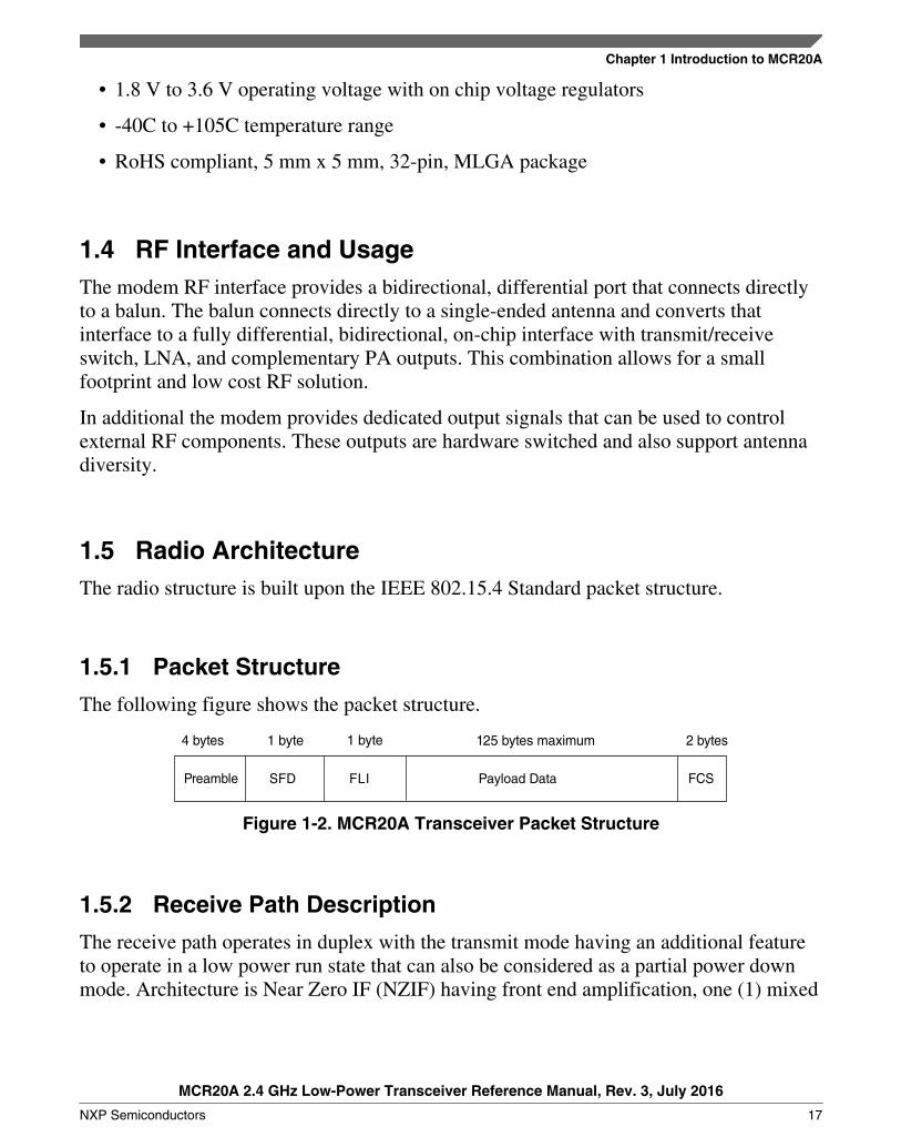
The following figure shows the packet structure.
Preamble SFD FLI Payload Data FCS
2 bytes125 bytes maximum1 byte1 byte4 bytes
Figure 1-2. MCR20A Transceiver Packet Structure
1.5.2 Receive Path Description
The receive path operates in duplex with the transmit mode having an additional featureto operate in a low power run state that can also be considered as a partial power downmode. Architecture is Near Zero IF (NZIF) having front end amplification, one (1) mixed
Chapter 1 Introduction to MCR20A
MCR20A 2.4 GHz Low-Power Transceiver Reference Manual, Rev. 3, July 2016
NXP Semiconductors 17
signal down conversion to IF that is filtered, demodulated and digitally processed. TheRF Front End (FE) is differential and shares the same off chip matching network with thetransmit path.
1.5.3 Transmit Path Description
The modem transmits OQPSK modulation having power and channel selectionadjustment per user application. After the channel of operation is determined, coarse andfine tuning is executed within the Frac-N PLL to engage signal lock. After signal lock isestablished, the modulated buffered signal is then routed to a multi-stage amplifier fortransmission. The PA differential outputs share the pins with the front end.
1.6 IEEE 802.15.4 Acceleration HardwareThe 802.15.4 transceiver has several hardware features that reduce the software stacksize, off-load functions from the CPU, and improve performance:
• Fully supports 2003 & 2006 versions of the IEEE 802.15 Standard.
• Supports slotted and unslotted modes
• Supports beacon enabled and non-beacon enabled networks
• Onboard 128-byte packet data buffering
• Random number generator
• 802.15.4 Sequence support
• RX (conditionally followed by TXAck)
• TX
• CCA (used for CCA and ED cycles)
• Tx/Rx (Tx followed by unconditional Rx or RCACK)
• Continuous CCA
• 802.15.4 Receiver Frame filtering.
IEEE 802.15.4 Acceleration Hardware
MCR20A 2.4 GHz Low-Power Transceiver Reference Manual, Rev. 3, July 2016
18 NXP Semiconductors
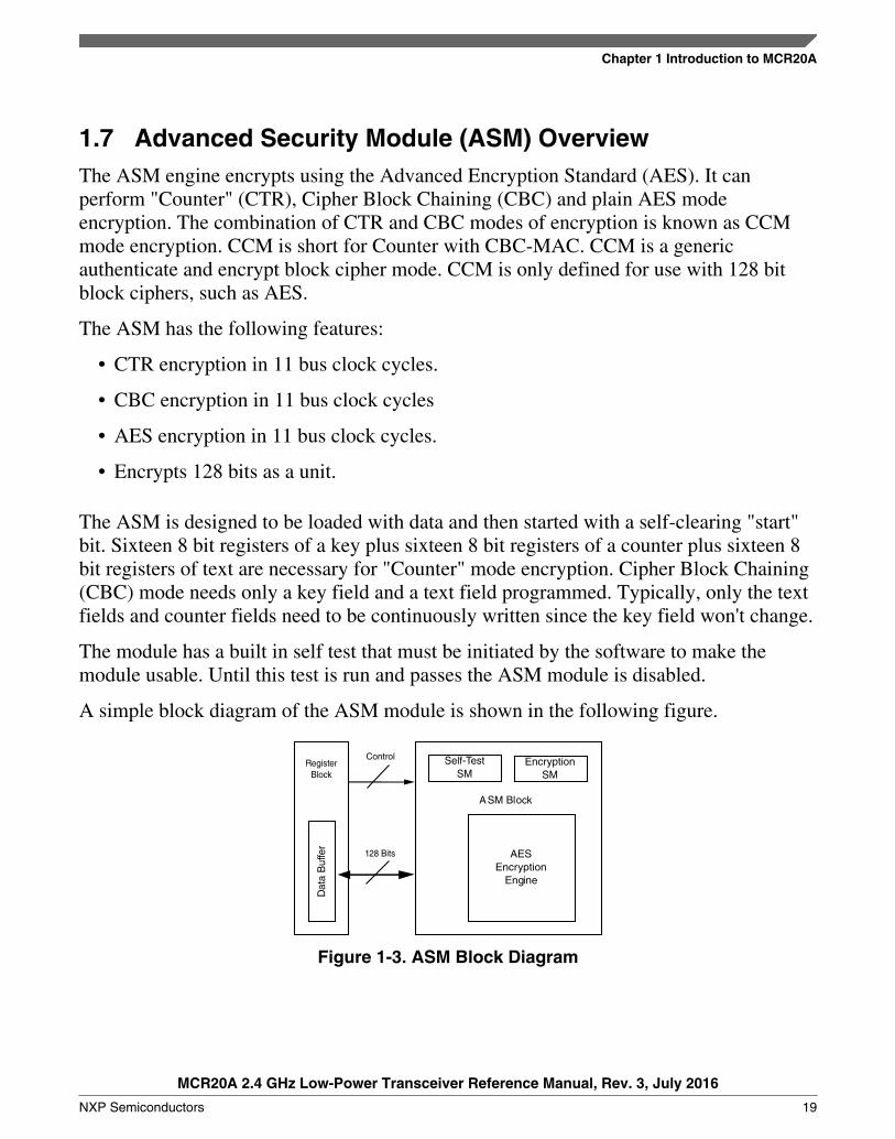
1.7 Advanced Security Module (ASM) OverviewThe ASM engine encrypts using the Advanced Encryption Standard (AES). It canperform "Counter" (CTR), Cipher Block Chaining (CBC) and plain AES modeencryption. The combination of CTR and CBC modes of encryption is known as CCMmode encryption. CCM is short for Counter with CBC-MAC. CCM is a genericauthenticate and encrypt block cipher mode. CCM is only defined for use with 128 bitblock ciphers, such as AES.
The ASM has the following features:
• CTR encryption in 11 bus clock cycles.
• CBC encryption in 11 bus clock cycles
• AES encryption in 11 bus clock cycles.
• Encrypts 128 bits as a unit.
The ASM is designed to be loaded with data and then started with a self-clearing "start"bit. Sixteen 8 bit registers of a key plus sixteen 8 bit registers of a counter plus sixteen 8bit registers of text are necessary for "Counter" mode encryption. Cipher Block Chaining(CBC) mode needs only a key field and a text field programmed. Typically, only the textfields and counter fields need to be continuously written since the key field won't change.
The module has a built in self test that must be initiated by the software to make themodule usable. Until this test is run and passes the ASM module is disabled.
A simple block diagram of the ASM module is shown in the following figure.
RegisterBlock
Control
128 Bits
Self-TestSM
EncryptionSM
A SM Block
AESEncryption
Engine
Dat
a B
uffe
r
Figure 1-3. ASM Block Diagram
Chapter 1 Introduction to MCR20A
MCR20A 2.4 GHz Low-Power Transceiver Reference Manual, Rev. 3, July 2016
NXP Semiconductors 19
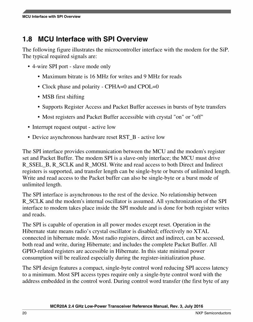
1.8 MCU Interface with SPI OverviewThe following figure illustrates the microcontroller interface with the modem for the SiP.The typical required signals are:
• 4-wire SPI port - slave mode only
• Maximum bitrate is 16 MHz for writes and 9 MHz for reads
• Clock phase and polarity - CPHA=0 and CPOL=0
• MSB first shifting
• Supports Register Access and Packet Buffer accesses in bursts of byte transfers
• Most registers and Packet Buffer accessible with crystal "on" or "off"
• Interrupt request output - active low
• Device asynchronous hardware reset RST_B - active low
The SPI interface provides communication between the MCU and the modem's registerset and Packet Buffer. The modem SPI is a slave-only interface; the MCU must driveR_SSEL_B, R_SCLK and R_MOSI. Write and read access to both Direct and Indirectregisters is supported, and transfer length can be single-byte or bursts of unlimited length.Write and read access to the Packet buffer can also be single-byte or a burst mode ofunlimited length.
The SPI interface is asynchronous to the rest of the device. No relationship betweenR_SCLK and the modem's internal oscillator is assumed. All synchronization of the SPIinterface to modem takes place inside the SPI module and is done for both register writesand reads.
The SPI is capable of operation in all power modes except reset. Operation in theHibernate state means radio’s crystal oscillator is disabled; effectively no XTALconnected in hibernate mode. Most radio registers, direct and indirect, can be accessed,both read and write, during Hibernate; and includes the complete Packet Buffer. AllGPIO-related registers are accessible in Hibernate. In this state minimal powerconsumption will be realized especially during the register-initialization phase.
The SPI design features a compact, single-byte control word reducing SPI access latencyto a minimum. Most SPI access types require only a single-byte control word with theaddress embedded in the control word. During control word transfer (the first byte of any
MCU Interface with SPI Overview
MCR20A 2.4 GHz Low-Power Transceiver Reference Manual, Rev. 3, July 2016
20 NXP Semiconductors
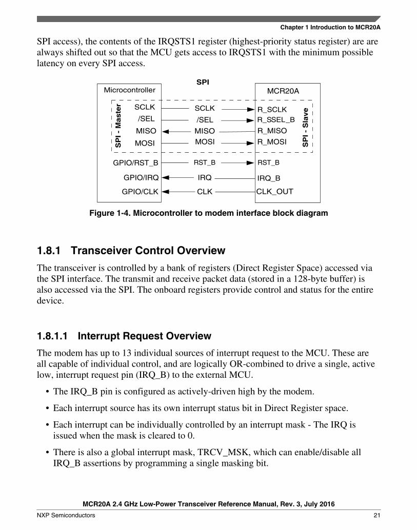
SPI access), the contents of the IRQSTS1 register (highest-priority status register) are arealways shifted out so that the MCU gets access to IRQSTS1 with the minimum possiblelatency on every SPI access.
MicrocontrollerSPI
SP
I -
Ma
ste
r SCLK
/SEL
MISO
MOSI
GPIO/RST_B
GPIO/IRQ
GPIO/CLK
MCR20A
SP
I -
Sla
veR_SCLK
R_SSEL_B
R_MISO
R_MOSI
RST_B
IRQ_B
CLK_OUT
SCLK
/SEL
MISO
MOSI
RST_B
IRQ
CLK
Figure 1-4. Microcontroller to modem interface block diagram
1.8.1 Transceiver Control Overview
The transceiver is controlled by a bank of registers (Direct Register Space) accessed viathe SPI interface. The transmit and receive packet data (stored in a 128-byte buffer) isalso accessed via the SPI. The onboard registers provide control and status for the entiredevice.
1.8.1.1 Interrupt Request Overview
The modem has up to 13 individual sources of interrupt request to the MCU. These areall capable of individual control, and are logically OR-combined to drive a single, activelow, interrupt request pin (IRQ_B) to the external MCU.
• The IRQ_B pin is configured as actively-driven high by the modem.
• Each interrupt source has its own interrupt status bit in Direct Register space.
• Each interrupt can be individually controlled by an interrupt mask - The IRQ isissued when the mask is cleared to 0.
• There is also a global interrupt mask, TRCV_MSK, which can enable/disable allIRQ_B assertions by programming a single masking bit.
Chapter 1 Introduction to MCR20A
MCR20A 2.4 GHz Low-Power Transceiver Reference Manual, Rev. 3, July 2016
NXP Semiconductors 21
• All status bits use a write-1-to-clear protocol - interrupt status bits are not affected byreads.
• IRQ_B will remain asserted until all active interrupt sources are cleared or masked.
1.8.1.2 Event Timer Overview
The modem features a 24-bit Event Timer that can be used in conjunction with thesequencer to provide protocol control as well as timing interrupts. The Event Timerconsists of a continuously running counter and four (4) separate 24-bit comparators:
• The Event Timer counter runs at the 802.15.4 bit rate of 250 kHz (programmable).
• Each comparator has an individual interrupt request capability - the compare status isset when there is a match between the comparator and the timer counter. Each statuscan be enabled to generate an IRQ.
• In addition, a separate 16-bit T2PRIMECMP comparator is provided, which usesonly the lower 16 bits of Event Timer, rather than require a full 24-bit compare.
1.9 Clock Output, RF Control, and GPIO SummaryThe modem provides a set of I/O pins useful for supplying a system clock to the MCU,controlling external RF LNA/PA or antenna diversity circuitry and GPIO. The followingsections discuss these options.
1.9.1 CLK_OUT Reference
The CLK_OUT digital output can be enabled to drive the system clock to the MCU. Thisprovides a highly accurate clock source based on the transceiver reference oscillator. Theclock is programmable over a wide range of frequencies divided down from its 32 MHzreference.
Clock Output, RF Control, and GPIO Summary
MCR20A 2.4 GHz Low-Power Transceiver Reference Manual, Rev. 3, July 2016
22 NXP Semiconductors

1.9.2 RF Control Signals
The modem provides four dedicated signals for control of external RF components.These signals designated as ANT_A, ANT_B, RX_SWITCH, and TX_SWITCH can beenabled to control external amplifiers, antenna switches, and other modules. Whenenabled they are switched via an internal hardware state machine. Typical uses include:
• Antenna diversity
• External PA
• External LNA
• T/R switching
1.9.3 Antenna Diversity
To improve the reliability of RF connectivity to long range applications, AntennaDiversity feature is supported without using the MCU through use of four dedicatedcontrol pins by direct register antenna selection. The digital regulator supplies bias toanalog switches for control of external PA/LNA. These switches are programmable tosink and source two levels of current (2-3 mA and 10 mA) or can operate in a highimpedance mode.
1.9.4 General Purpose Input Output (GPIO)
In addition eight (8) GPIO are provided for general use. Features for these pins include:
• Programmable output drive strength
• Programmable output slew rate
• Hi-Z mode
• Programmable as outputs or inputs (default)
• No IRQ capability
1.10 Modem Operational ModesThe modem has six operating modes which include:
Chapter 1 Introduction to MCR20A
MCR20A 2.4 GHz Low-Power Transceiver Reference Manual, Rev. 3, July 2016
NXP Semiconductors 23
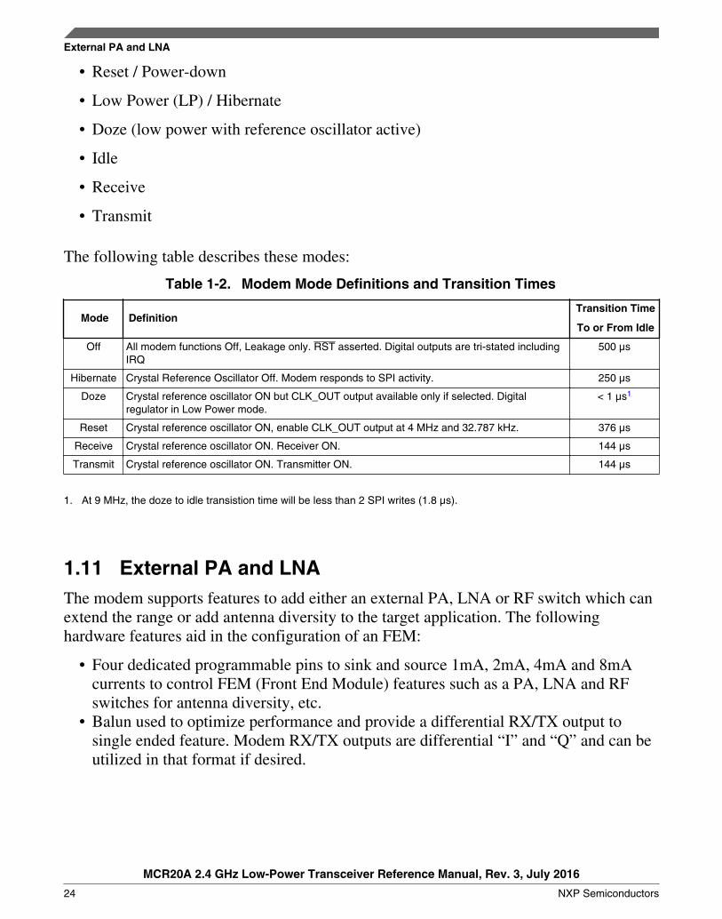
• Reset / Power-down
• Low Power (LP) / Hibernate
• Doze (low power with reference oscillator active)
• Idle
• Receive
• Transmit
The following table describes these modes:
Table 1-2. Modem Mode Definitions and Transition Times
Mode DefinitionTransition Time
To or From Idle
Off All modem functions Off, Leakage only. RST asserted. Digital outputs are tri-stated includingIRQ
500 μs
Hibernate Crystal Reference Oscillator Off. Modem responds to SPI activity. 250 μs
Doze Crystal reference oscillator ON but CLK_OUT output available only if selected. Digitalregulator in Low Power mode.
< 1 μs1
Reset Crystal reference oscillator ON, enable CLK_OUT output at 4 MHz and 32.787 kHz. 376 μs
Receive Crystal reference oscillator ON. Receiver ON. 144 μs
Transmit Crystal reference oscillator ON. Transmitter ON. 144 μs
1. At 9 MHz, the doze to idle transistion time will be less than 2 SPI writes (1.8 μs).
1.11 External PA and LNAThe modem supports features to add either an external PA, LNA or RF switch which canextend the range or add antenna diversity to the target application. The followinghardware features aid in the configuration of an FEM:
• Four dedicated programmable pins to sink and source 1mA, 2mA, 4mA and 8mAcurrents to control FEM (Front End Module) features such as a PA, LNA and RFswitches for antenna diversity, etc.
• Balun used to optimize performance and provide a differential RX/TX output tosingle ended feature. Modem RX/TX outputs are differential “I” and “Q” and can beutilized in that format if desired.
External PA and LNA
MCR20A 2.4 GHz Low-Power Transceiver Reference Manual, Rev. 3, July 2016
24 NXP Semiconductors
Chapter 2Signal Multiplexing and Signal Descriptions
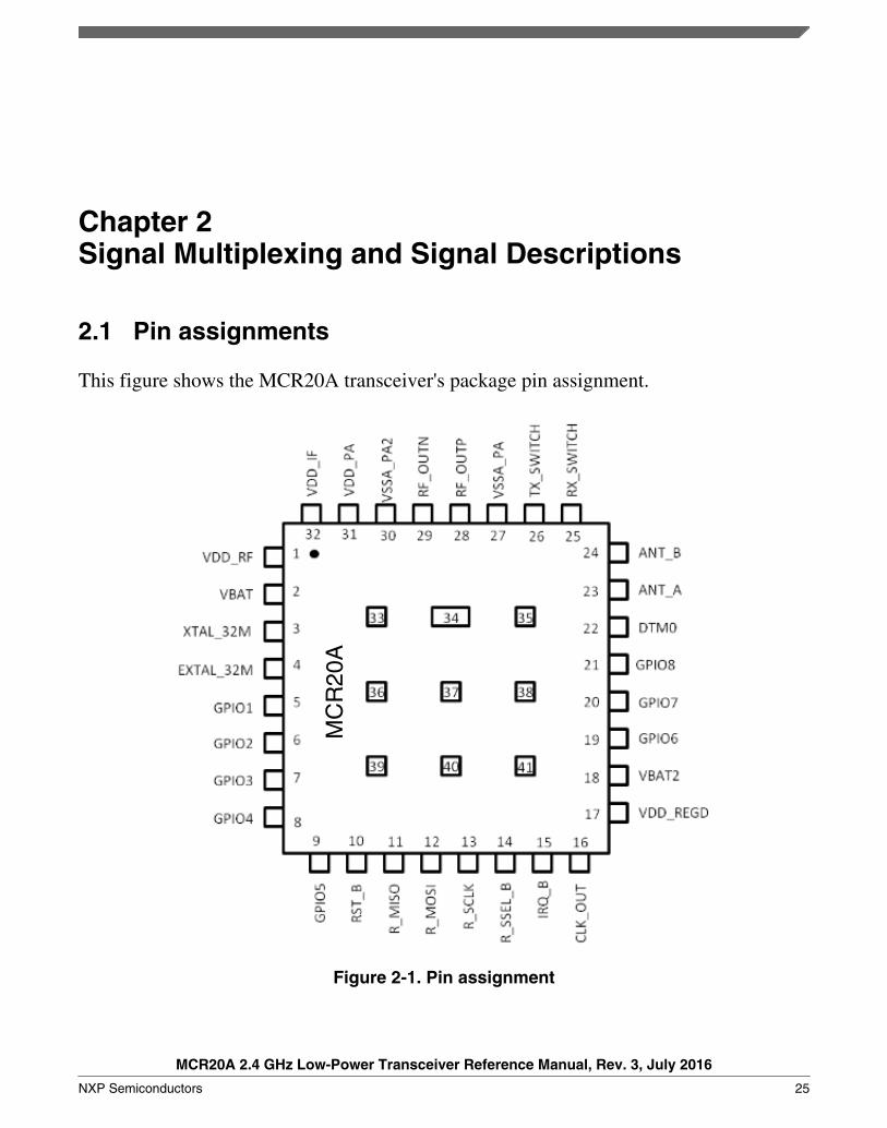
2.1 Pin assignments
This figure shows the MCR20A transceiver's package pin assignment.
MC
R20
A
Figure 2-1. Pin assignment
MCR20A 2.4 GHz Low-Power Transceiver Reference Manual, Rev. 3, July 2016
NXP Semiconductors 25
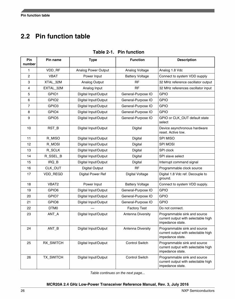
2.2 Pin function table
Table 2-1. Pin function
Pinnumber
Pin name Type Function Description
1 VDD_RF Analog Power Output Analog Voltage Analog 1.8 Vdc
2 VBAT Power Input Battery Voltage Connect to system VDD supply
3 XTAL_32M Analog Output RF 32 MHz reference oscillator output
4 EXTAL_32M Analog Input RF 32 MHz references oscillator input
5 GPIO1 Digital Input/Output General-Purpose IO GPIO
6 GPIO2 Digital Input/Output General-Purpose IO GPIO
7 GPIO3 Digital Input/Output General-Purpose IO GPIO
8 GPIO4 Digital Input/Output General-Purpose IO GPIO
9 GPIO5 Digital Input/Output General-Purpose IO GPIO or CLK_OUT default stateselect
10 RST_B Digital Input/Output Digital Device asynchronous hardwarereset. Active low.
11 R_MISO Digital Input/Output Digital SPI MISO
12 R_MOSI Digital Input/Output Digital SPI MOSI
13 R_SCLK Digital Input/Output Digital SPI clock
14 R_SSEL_B Digital Input/Output Digital SPI slave select
15 IRQ_B Digital Input/Output Digital Interrupt command signal
16 CLK_OUT Digital Output RF Programmable clock source
17 VDD_REGD Digital Power Ref Digital Voltage Digital 1.8 Vdc ref. Decouple toground.
18 VBAT2 Power Input Battery Voltage Connect to system VDD supply.
19 GPIO6 Digital Input/Output General-Purpose IO GPIO
20 GPIO7 Digital Input/Output General-Purpose IO GPIO
21 GPIO8 Digital Input/Output General-Purpose IO GPIO
22 DTM0 — Factory Test Do not connect.
23 ANT_A Digital Input/Output Antenna Diversity Programmable sink and sourcecurrent output with selectable highimpedance state.
24 ANT_B Digital Input/Output Antenna Diversity Programmable sink and sourcecurrent output with selectable highimpedance state.
25 RX_SWITCH Digital Input/Output Control Switch Programmable sink and sourcecurrent output with selectable highimpedance state.
26 TX_SWITCH Digital Input/Output Control Switch Programmable sink and sourcecurrent output with selectable highimpedance state.
Table continues on the next page...
Pin function table
MCR20A 2.4 GHz Low-Power Transceiver Reference Manual, Rev. 3, July 2016
26 NXP Semiconductors
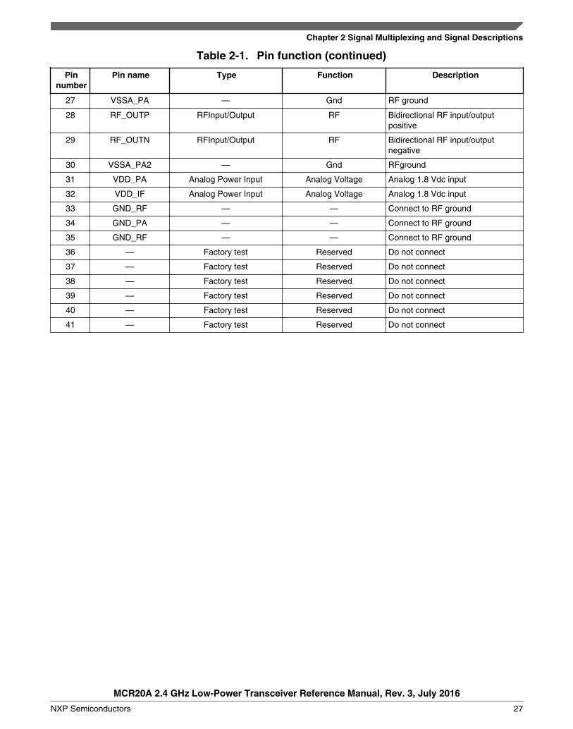
Table 2-1. Pin function (continued)
Pinnumber
Pin name Type Function Description
27 VSSA_PA — Gnd RF ground
28 RF_OUTP RFInput/Output RF Bidirectional RF input/outputpositive
29 RF_OUTN RFInput/Output RF Bidirectional RF input/outputnegative
30 VSSA_PA2 — Gnd RFground
31 VDD_PA Analog Power Input Analog Voltage Analog 1.8 Vdc input
32 VDD_IF Analog Power Input Analog Voltage Analog 1.8 Vdc input
33 GND_RF — — Connect to RF ground
34 GND_PA — — Connect to RF ground
35 GND_RF — — Connect to RF ground
36 — Factory test Reserved Do not connect
37 — Factory test Reserved Do not connect
38 — Factory test Reserved Do not connect
39 — Factory test Reserved Do not connect
40 — Factory test Reserved Do not connect
41 — Factory test Reserved Do not connect
Chapter 2 Signal Multiplexing and Signal Descriptions
MCR20A 2.4 GHz Low-Power Transceiver Reference Manual, Rev. 3, July 2016
NXP Semiconductors 27

Pin function table
MCR20A 2.4 GHz Low-Power Transceiver Reference Manual, Rev. 3, July 2016
28 NXP Semiconductors
Chapter 3System Considerations
3.1 IntroductionCommunication to the modem function is through the common SPI bus, the MCUinterrupt request, and several MCU GPIO lines. Primary interface with the modem isthrough the SPI command structure that allows reading/writing modem registers andprovides initialization of parameters, reading of status, and control of modem operation.The modem can ask for real time response through the interrupt request structure, andfour GPIO signals allow control of the modem reset and monitoring of some real timestatus.
This chapter presents information addressing application and operation of the node froma system level. The areas considered here are also covered in greater detail in thefollowing sections of the book. The book is organized such that the first three chapterspresent the top-level view of the MCR20A device and the following chapters presentindividual functions in detailed descriptions.
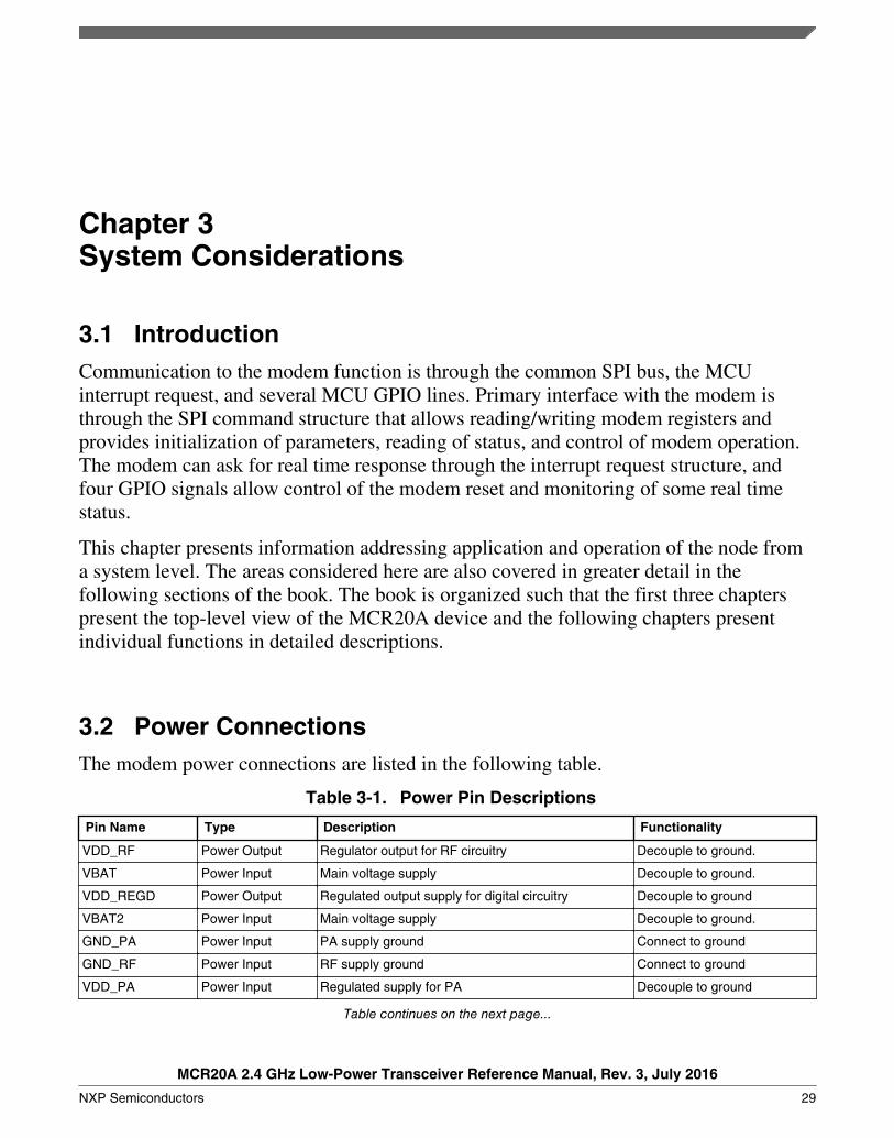
3.2 Power ConnectionsThe modem power connections are listed in the following table.
Table 3-1. Power Pin Descriptions
Pin Name Type Description Functionality
VDD_RF Power Output Regulator output for RF circuitry Decouple to ground.
VBAT Power Input Main voltage supply Decouple to ground.
VDD_REGD Power Output Regulated output supply for digital circuitry Decouple to ground
VBAT2 Power Input Main voltage supply Decouple to ground.
GND_PA Power Input PA supply ground Connect to ground
GND_RF Power Input RF supply ground Connect to ground
VDD_PA Power Input Regulated supply for PA Decouple to ground
Table continues on the next page...
MCR20A 2.4 GHz Low-Power Transceiver Reference Manual, Rev. 3, July 2016
NXP Semiconductors 29
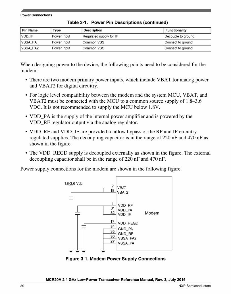
Table 3-1. Power Pin Descriptions (continued)
Pin Name Type Description Functionality
VDD_IF Power Input Regulated supply for IF Decouple to ground
VSSA_PA Power Input Common VSS Connect to ground
VSSA_PA2 Power Input Common VSS Connect to ground
When designing power to the device, the following points need to be considered for themodem:
• There are two modem primary power inputs, which include VBAT for analog powerand VBAT2 for digital circuitry.
• For logic level compatibility between the modem and the system MCU, VBAT, andVBAT2 must be connected with the MCU to a common source supply of 1.8–3.6VDC. It is not recommended to supply the MCU below 1.8V.
• VDD_PA is the supply of the internal power amplifier and is powered by theVDD_RF regulator output via the analog regulator.
• VDD_RF and VDD_IF are provided to allow bypass of the RF and IF circuitryregulated supplies. The decoupling capacitor is in the range of 220 nF and 470 nF asshown in the figure.
• The VDD_REGD supply is decoupled externally as shown in the figure. The externaldecoupling capacitor shall be in the range of 220 nF and 470 nF.
Power supply connections for the modem are shown in the following figure.
VDD_IF Modem
1.8-3.6 Vdc2
18
13132
17
VDD_RF
VBATVBAT2
VDD_PA
VDD_REGD
VSSA_PA
34353027
VSSA_PA2GND_RFGND_PA
Figure 3-1. Modem Power Supply Connections
Power Connections
MCR20A 2.4 GHz Low-Power Transceiver Reference Manual, Rev. 3, July 2016
30 NXP Semiconductors
NOTE
In addition to the capacitor on the VBATs, there are twoseparate decoupling capacitors, one on VDD_RF, VDD_IF, andVDD_PA that are tied together, and a standalone onVDD_REGD.
3.3 Modem Reset
The modem active low reset input RST_B is recommended to be driven from an MCUGPIO pin. In the interest of lowest power, there is no external pull-up resistor on inputRST_B. An MCU GPIO programmed as an output typically also has a softwarecontrolled pull-up resistor. However, it would normally not be used because the modemcan be held in hardware reset by the MCU for extended periods of time. The transceiverIRQ pullup can also be disabled, and having no resistor makes for lowest powerapplications.
From a power-on or “cold start” condition, the MCU GPIO normally initiates as a high-impedance input with its internal pullup disabled and the IRQ pullup is enabled, whichholds the modem reset input high. As part of the MCU initialization, GPIO must beprogrammed as an output and then driven low to reset the modem. The RST_B input isasynchronous and needs to be held low for only a short period.
• The MCU software must configure one of its GPIOs as an output and then drive itlow to reset the modem.
During the modem reset procedure,• The MCU software should also configure the I/O port driving GPIO5 to select the
default modem CLK_OUT frequency (GPIO5 high = 32.787 kHz; GPIO5 low = 4MHz).
• The modem RST_B input is asynchronous and needs to be held low for only a shortperiod.
In the reset condition, the modem is totally powered down and no clocks are available.After RST_B is released, the modem will power up, initialize, and go to its idle conditionin less than 1 millisecond, and in turn, this causes an IRQ_B interrupt request and allowsCLK_OUT to start toggling. Coming out of reset, the WAKE_IRQ interrupt status bit isset and causes the assertion on the IRQ_B because the wake interrupt source is notmasked by default.
Once the interrupt request is seen by the MCU, the MCU can assume the modem is aliveand ready for programming via the SPI bus.
Chapter 3 System Considerations
MCR20A 2.4 GHz Low-Power Transceiver Reference Manual, Rev. 3, July 2016
NXP Semiconductors 31
3.4 Modem Interrupt Request to MCUThe modem interrupt request IRQ_B is an active low output that is asserted when aninterrupt request is pending. The signal is released to high by writing a 1 to all assertedinterrupt status bits in the modem status registers via a SPI transaction.
3.5 MCR20A Transceiver Interface to MCUThe modem interacts with the host MCU through its SPI interface, interrupt request, andseveral status and control signals.
3.5.1 SPI Command Channel
Primary interface with the modem is through the SPI command structure that allowsreading/writing modem registers and provides initialization of parameters, reading ofstatus, and control of modem operation. The modem is a slave only and the MCU SPImust be programmed and used as a master only. Further, the SPI performance is limitedby the modem constraints of 8 MHz maximum SPI clock frequency, and use of the MCUSPI must be programmed to meet the modem SPI protocol. The SPI bus connections for aKinetis K20-512 typically are:
• MCU MOSI output drives modem R_MOSI.• Modem R_MISO output drives MCU MISO.• MCU SCLK output drives modem R_SCLK.• MCU /SELoutput drives modem R_SSEL_B.
System Oscillator and Clock Considerations
3.6.1 Modem Crystal Oscillator
The modem oscillator source must always be present and an external crystal is used toimplement the oscillator. The source frequency must be 32 MHz with a total accuracy of±40 ppm or greater as required by the IEEE 802.15.4 specification.
3.6
Modem Interrupt Request to MCU
MCR20A 2.4 GHz Low-Power Transceiver Reference Manual, Rev. 3, July 2016
32 NXP Semiconductors
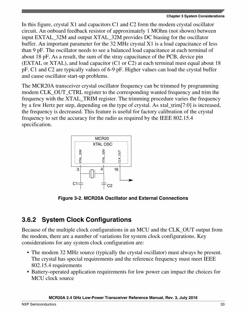
In this figure, crystal X1 and capacitors C1 and C2 form the modem crystal oscillatorcircuit. An onboard feedback resistor of approximately 1 MOhm (not shown) betweeninput EXTAL_32M and output XTAL_32M provides DC biasing for the oscillatorbuffer. An important parameter for the 32 MHz crystal X1 is a load capacitance of lessthan 9 pF. The oscillator needs to see a balanced load capacitance at each terminal ofabout 18 pF. As a result, the sum of the stray capacitance of the PCB, device pin(EXTAL or XTAL), and load capacitor (C1 or C2) at each terminal must equal about 18pF. C1 and C2 are typically values of 6-9 pF. Higher values can load the crystal bufferand cause oscillator start-up problems.
The MCR20A transceiver crystal oscillator frequency can be trimmed by programmingmodem CLK_OUT_CTRL register to the corresponding wanted frequency and trim thefrequency with the XTAL_TRIM register. The trimming procedure varies the frequencyby a few Hertz per step, depending on the type of crystal. As xtal_trim[7:0] is increased,the frequency is decreased. This feature is useful for factory calibration of the crystalfrequency to set the accuracy for the radio as required by the IEEE 802.15.4specification.
MCR20XTAL OSC
C1 C2
3 4 16
XTA
L_32
M
XTA
L_32
M
CLK
_OU
T
Figure 3-2. MCR20A Oscillator and External Connections
3.6.2 System Clock Configurations
Because of the multiple clock configurations in an MCU and the CLK_OUT output fromthe modem, there are a number of variations for system clock configurations. Keyconsiderations for any system clock configuration are:
• The modem 32 MHz source (typically the crystal oscillator) must always be present.The crystal has special requirements and the reference frequency must meet IEEE802.15.4 requirements
• Battery-operated application requirements for low power can impact the choices forMCU clock source
Chapter 3 System Considerations
MCR20A 2.4 GHz Low-Power Transceiver Reference Manual, Rev. 3, July 2016
NXP Semiconductors 33
• The system clock configuration can impact system initialization procedures• Software requirements can impact MCU processor and bus speed. The user must be
aware of the performance requirements for the MCU.
3.6.3 Single System Crystal with CLK_OUT driving MCU crystalinput
The single crystal (modem crystal) with CLK_OUT driving the MCU external clockinput is a common configuration for low cost and excellent frequency accuracy. TheCLK_OUT frequency is programmable from 32.786 kHz to 32 MHz and drives the MCUexternal source.
Note
For this system option to be usable, the system MCU must havean alternative (typically onboard) start-up clock.
In this configuration, clock start-up from a reset condition involves:
• MCU reset is released and MCU starts on an internal clock• Initialization software must reset and then release reset to the modem (MCU still
running on start-up clock)• Wait for modem start-up interrupt request (less than 1 ms). CLK_OUT default is
hardware selectable as either 4 MHz or 32.786 kHz defined by the state of modemGPIO5.
• Program CLK_OUT to a different frequency (if desired) as shown in the table.• Wait for the CLK_OUT source to lock, and then switch MCU clock to external
source
Additional considerations for this mode of operation include:
• If the modem is forced to the Off condition and CLK_OUT is killed, there is a 500 μswait for the modem CLK_OUT to start from the Off condition after RST is released
• If the MCU puts the modem into Doze mode, keeping the CLK_OUT alive is ahigher power, but available, option
• If an accurate period is required for longer time delays (such as a beacon period),keeping CLK alive for very long periods is an option, but would be a higher poweroption typically than using a separate crystal for the MCU
3.7 Modem GPIO Characteristics
Modem GPIO Characteristics
MCR20A 2.4 GHz Low-Power Transceiver Reference Manual, Rev. 3, July 2016
34 NXP Semiconductors
The modem GPIO hardware consists of eight (8) signals total (GPIO1-GPIO8) thoughonly GPIO1-6 are used in the SIP, and only GPIO1-2 are connected directly to SIPpackage pins. Immediately after reset, each GPIO has either an internal pull-up(GPIO1-5) or pull-down (GPIO6-8) enabled.
NOTETo avoid extra current drain from floating input pins, the resetinitialization routine in the application program should changethe direction of unused pins to outputs (programmed low) sothe pins do not float. Outputs programmed low is the preferredoption for lowest power.
The functionality of the modem GPIO is controlled by programming of the modem SPIregisters via the SPI interface. For information about controlling all these pins as generalpurpose I/O pins, see SPI Register Descriptions chapter.
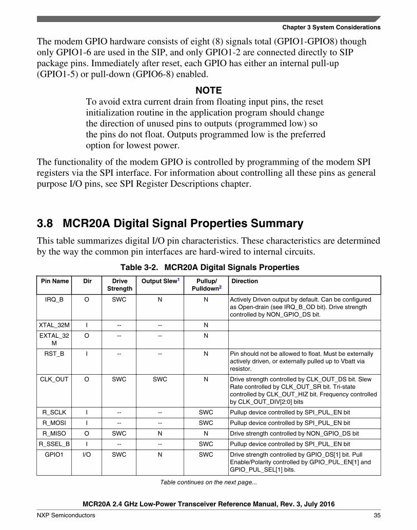
3.8 MCR20A Digital Signal Properties SummaryThis table summarizes digital I/O pin characteristics. These characteristics are determinedby the way the common pin interfaces are hard-wired to internal circuits.
Table 3-2. MCR20A Digital Signals Properties
Pin Name Dir DriveStrength
Output Slew1 Pullup/Pulldown2
Direction
IRQ_B O SWC N N Actively Driven output by default. Can be configuredas Open-drain (see IRQ_B_OD bit). Drive strengthcontrolled by NON_GPIO_DS bit.
XTAL_32M I -- -- N
EXTAL_32M
O -- -- N
RST_B I -- -- N Pin should not be allowed to float. Must be externallyactively driven, or externally pulled up to Vbatt viaresistor.
CLK_OUT O SWC SWC N Drive strength controlled by CLK_OUT_DS bit. SlewRate controlled by CLK_OUT_SR bit. Tri-statecontrolled by CLK_OUT_HIZ bit. Frequency controlledby CLK_OUT_DIV[2:0] bits
R_SCLK I -- -- SWC Pullup device controlled by SPI_PUL_EN bit
R_MOSI I -- -- SWC Pullup device controlled by SPI_PUL_EN bit
R_MISO O SWC N N Drive strength controlled by NON_GPIO_DS bit
R_SSEL_B I -- -- SWC Pullup device controlled by SPI_PUL_EN bit
GPIO1 I/O SWC N SWC Drive strength controlled by GPIO_DS[1] bit. PullEnable/Polarity controlled by GPIO_PUL_EN[1] andGPIO_PUL_SEL[1] bits.
Table continues on the next page...
Chapter 3 System Considerations
MCR20A 2.4 GHz Low-Power Transceiver Reference Manual, Rev. 3, July 2016
NXP Semiconductors 35
Table 3-2. MCR20A Digital Signals Properties (continued)
Pin Name Dir DriveStrength
Output Slew1 Pullup/Pulldown2
Direction
GPIO2 I/O SWC N SWC Drive strength controlled by GPIO_DS[2] bit. PullEnable/Polarity controlled by GPIO_PUL_EN[2] andGPIO_PUL_SEL[2] bits.
GPIO3 I/O SWC N SWC Drive strength controlled by GPIO_DS[3] bit. PullEnable/Polarity controlled by GPIO_PUL_EN[3] andGPIO_PUL_SEL[3] bits.
GPIO4 I/O SWC N SWC Drive strength controlled by GPIO_DS[4] bit. PullEnable/Polarity controlled by GPIO_PUL_EN[4] andGPIO_PUL_SEL[4] bits.
GPIO5 I/O SWC N SWC Drive strength controlled by GPIO_DS[5] bit. PullEnable/Polarity controlled by GPIO_PUL_EN[5] andGPIO_PUL_SEL[5] bits.
GPIO6 I/O SWC N SWC Drive strength controlled by GPIO_DS[6] bit. PullEnable/Polarity controlled by GPIO_PUL_EN[6] andGPIO_PUL_SEL[6] bits.
GPIO7 I/O SWC N SWC Drive strength controlled by GPIO_DS[7] bit. PullEnable/Polarity controlled by GPIO_PUL_EN[7] andGPIO_PUL_SEL[7] bits.
GPIO8 I/O SWC N SWC Drive strength controlled by GPIO_DS[8] bit. PullEnable/Polarity controlled by GPIO_PUL_EN[8] andGPIO_PUL_SEL[8] bits.
1. Slew Rate Controlled: N=No; SWC=software-controlled2. Internal pullup/pulldown device: N=No; SWC=software-controlled
3.9 Transceiver RF Configurations and External ConnectionsThe MCR20A transceiver radio has features that enable a flexible and low cost RFinterface:
• Programmable output power from –35 dBm to +8 dBm. This allows the user to setthe power based on their specific applications minimizing current consumption whilemaximizing battery life.
• –102 dBm (typical) receive sensitivity — At 1% PER, 20-byte packet (well aboveIEEE 802.15.4 specification of –85 dBm).
• Integrated transmit/receive (T/R) switch for low cost operation — With internal PAsand LNA, the internal T/R switch allows a minimal part count radio interface usingonly a single balun to interface to a single-ended antenna.
Transceiver RF Configurations and External Connections
MCR20A 2.4 GHz Low-Power Transceiver Reference Manual, Rev. 3, July 2016
36 NXP Semiconductors
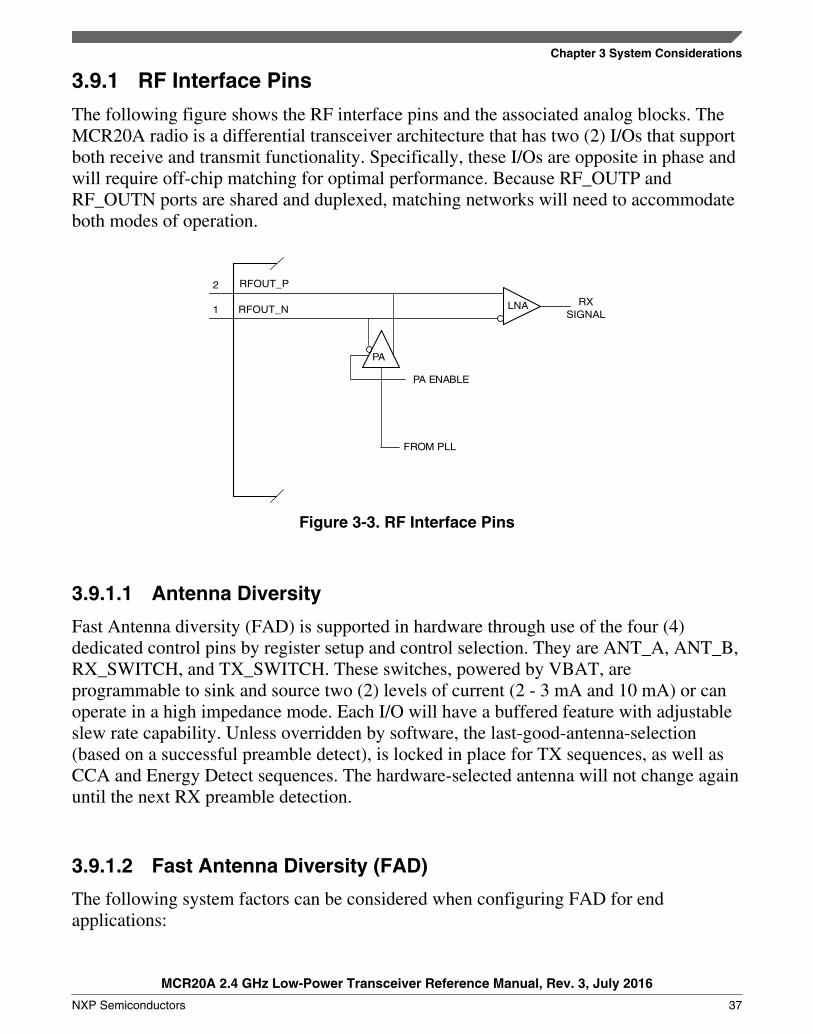
3.9.1 RF Interface Pins
The following figure shows the RF interface pins and the associated analog blocks. TheMCR20A radio is a differential transceiver architecture that has two (2) I/Os that supportboth receive and transmit functionality. Specifically, these I/Os are opposite in phase andwill require off-chip matching for optimal performance. Because RF_OUTP andRF_OUTN ports are shared and duplexed, matching networks will need to accommodateboth modes of operation.
RFOUT_P
RFOUT_N
2
1
PA
LNA RXSIGNAL
PA ENABLE
FROM PLL
Figure 3-3. RF Interface Pins
3.9.1.1 Antenna Diversity
Fast Antenna diversity (FAD) is supported in hardware through use of the four (4)dedicated control pins by register setup and control selection. They are ANT_A, ANT_B,RX_SWITCH, and TX_SWITCH. These switches, powered by VBAT, areprogrammable to sink and source two (2) levels of current (2 - 3 mA and 10 mA) or canoperate in a high impedance mode. Each I/O will have a buffered feature with adjustableslew rate capability. Unless overridden by software, the last-good-antenna-selection(based on a successful preamble detect), is locked in place for TX sequences, as well asCCA and Energy Detect sequences. The hardware-selected antenna will not change againuntil the next RX preamble detection.
3.9.1.2 Fast Antenna Diversity (FAD)
The following system factors can be considered when configuring FAD for endapplications:
Chapter 3 System Considerations
MCR20A 2.4 GHz Low-Power Transceiver Reference Manual, Rev. 3, July 2016
NXP Semiconductors 37
• With Fast Antenna Diversity, sensitivity performance increases the low-end limit ofthe dynamic range of the system.
• There is little cost of FAD which is essentially enabling the functionality and addingthe circuitry for situations where the application runs the possibility of operating atthe limits of RX sensitivity.
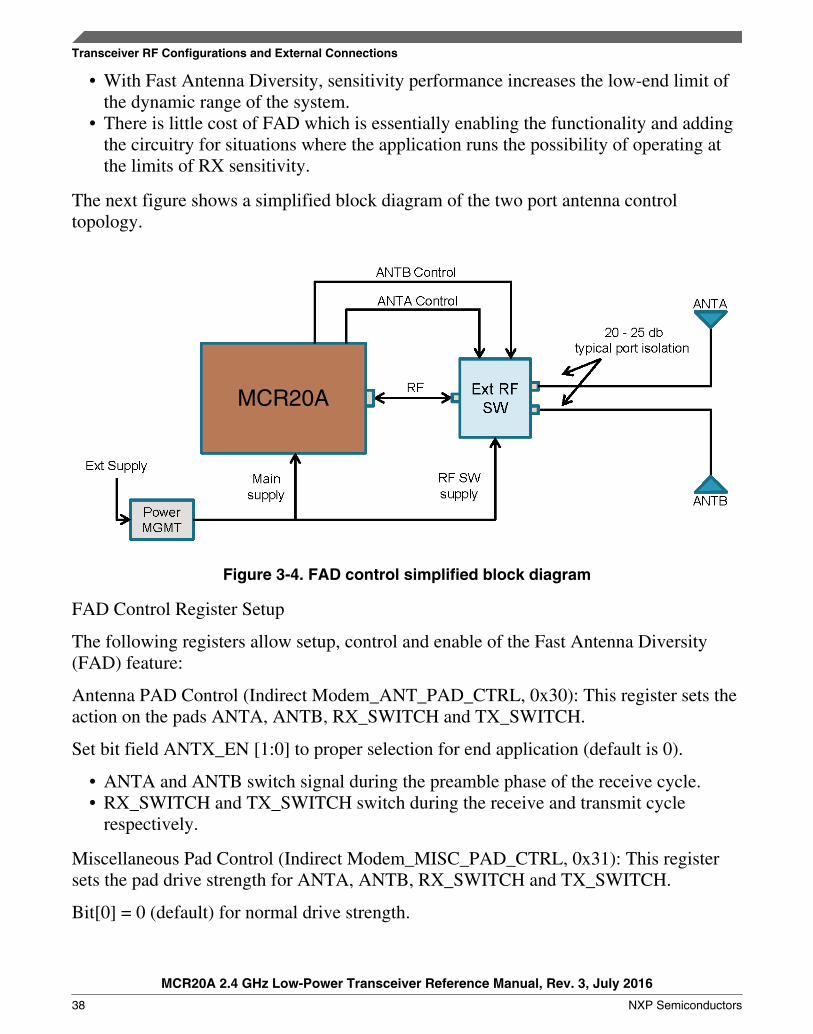
The next figure shows a simplified block diagram of the two port antenna controltopology.
MCR20A
Figure 3-4. FAD control simplified block diagram
FAD Control Register Setup
The following registers allow setup, control and enable of the Fast Antenna Diversity(FAD) feature:
Antenna PAD Control (Indirect Modem_ANT_PAD_CTRL, 0x30): This register sets theaction on the pads ANTA, ANTB, RX_SWITCH and TX_SWITCH.
Set bit field ANTX_EN [1:0] to proper selection for end application (default is 0).
• ANTA and ANTB switch signal during the preamble phase of the receive cycle.• RX_SWITCH and TX_SWITCH switch during the receive and transmit cycle
respectively.
Miscellaneous Pad Control (Indirect Modem_MISC_PAD_CTRL, 0x31): This registersets the pad drive strength for ANTA, ANTB, RX_SWITCH and TX_SWITCH.
Bit[0] = 0 (default) for normal drive strength.
Transceiver RF Configurations and External Connections
MCR20A 2.4 GHz Low-Power Transceiver Reference Manual, Rev. 3, July 2016
38 NXP Semiconductors
Antenna AGC and FAD Control (Indirect Modem_ANT_AGC_CTRL , 0x51): Thisregister controls the FAD feature.
Enable bit field [0] to 1 - Turns FAD on (default is 0).
The following figure shows the flow and timing diagram from the idle state when thereceiver takes either the FAD RX flow or the standard RX flow:
Figure 3-5. FAD flow and timing diagram
FAD and Packet Timing
Packet timing with FAD enabled with two external antenna’s A and B.
During the time period t1 – t0, the antenna’s are switching at a rate of 28 μs.
• The circular region shows the timing variation while detecting 1.5 symbol ‘0’s and isa function of system sensitivity level.
• At t1, the ‘first’ antenna meeting the 1.5 symbol ‘0’ criteria is selected … 3 moresymbol ‘0’s are then detected to complete the preamble search.
Normal packet processing follows a good preamble match
• The preamble period t2 – t0 is fixed at 128 μs of the total packet cycle time – if avalid preamble is not found during this period, the receiver will start a new RX cycle.
Chapter 3 System Considerations
MCR20A 2.4 GHz Low-Power Transceiver Reference Manual, Rev. 3, July 2016
NXP Semiconductors 39
Figure 3-6. FAD preamble and packet timing
The next figure shows a typical FAD control pin design topology
Figure 3-7. Typical circuitry for a two-antenna external switch design
The following figure shows a simulated out of range antenna scenario when using theisolation through an RF switch to offset the RF signal by 21 dBm. The followingsensitivity performance summary explains non-FAD and FAD Enabled SensitivityImprovement.
Transceiver RF Configurations and External Connections
MCR20A 2.4 GHz Low-Power Transceiver Reference Manual, Rev. 3, July 2016
40 NXP Semiconductors
Figure 3-8. Sensitivity FAD mode at 2450 MHz
Sensitivity Performance Summary
Non-FAD mode
• By purposely choosing the bad antenna (out of range RF signal) it can be seen(orange curve) that the sensitivity is shifted to –78 dBm.
• By purposely choosing the good antenna (RF signal in range) it can be seen (bluecurve) that the sensitivity is normal.
• The sensitivity delta is due to the isolation characteristics of the external RF switchcomponent. This is the basic limitation of the system. The isolation of the RF switchports in most cases is between 20-25 dB.
With FAD enabled (purple curve): With one antenna out of range and the other antennagood, the sensitivity is NOW in the normal range (about -99 dBm or better).
• Sensitivity performance is impacted by 1-2 dB in FAD mode vs. an ideally placedantenna but overall PER performance is significantly increased vs. having a singleantenna with poor placement.
• Within the dynamic range of the receiver, sensitivity in FAD mode does not impactperformance and therefore is not discernible to the user.
Chapter 3 System Considerations
MCR20A 2.4 GHz Low-Power Transceiver Reference Manual, Rev. 3, July 2016
NXP Semiconductors 41

• Outside the dynamic range of the receiver is where FAD will help systemperformance and will have noticeable improvements to the system.
• Unless overridden by software, the last-good-antenna-selection (based on asuccessful preamble detect), is locked in place for TX sequences as well as CCA andEnergy Detect sequences. The hardware-selected antenna will not change again untilthe next RX sequence.
3.9.2 RF Output Power Distribution
The following figure shows the linear region of the output and the typical powerdistribution of the radio as a function of PA_PWR [4:0] range. The PA_PWR [4:0] is thelower 5 bits of the PA_PWR 0x23 direct register and has a usable range of 3 to 31decimal.
Figure 3-9. MCR20A transmit power vs. PA_PWR step
Transceiver RF Configurations and External Connections
MCR20A 2.4 GHz Low-Power Transceiver Reference Manual, Rev. 3, July 2016
42 NXP Semiconductors
3.9.3 LQI ED RSSI
The following figure shows the devices reported Energy Detect (ED) as a function ofinput power. The figure also shows the Link Quality Indication (LQI)/RSSI_CONT(continuous) and the RSSI (Received Signal Strength Indication) as a function of aunitless numeric register reading. LQI is available 64 μs after the preamble is detected.RSSI_CONT can be used to read LQI if a continuous value averaged over the entirereceived packet is desired. This value may be read as LQI if continuous update of LQI isdesired during packet reception (both scaled the same but averaged differently). Thecurves are measured using the default offset compensation value and can be changed tocenter the curve if desired.
The following sequeces are performed in test software to create curves in the figureotherwise similar sequences are incorporated into our software stacks:
• For ED, device is configured to perform an ED via write to the register 0x7 with0x00
• ED/CCA sequence is started via write to register 0x3 with 0x3
• Register 0 is polled for bit 3 to be set
• RSSI_CONT_EN bit is disabled in Indirect 0x25 (CCA_CTRL) all other bits arereset/overwrite values
• direct register 0x0B is read (CCA Final)
• direct register 0x25 is read (LQI)
• indirect register 0x5B is read (RSSI)
• direct register 0x26 is read (RSSI_CONT) [not enabled in ED case so ignored]
• For LQI, device is configured to perform an LQI via write to the register 0x7 with0x00
• Device is configured to perform an LQI via write to the register 0x7 with 0x00
• RX sequence is started via write to register 0x3 with 0x1
• Register 0 is polled for bit 2 to be set
• RSSI_CONT_EN bit is Enabled in Indirect 0x25
• RSSI_CONT_EN bit is disabled in Indirect 0x25 (CCA_CTRL) all other bits arereset/overwrite values
• Direct register 0x0B is read (CCA Final)
Chapter 3 System Considerations
MCR20A 2.4 GHz Low-Power Transceiver Reference Manual, Rev. 3, July 2016
NXP Semiconductors 43
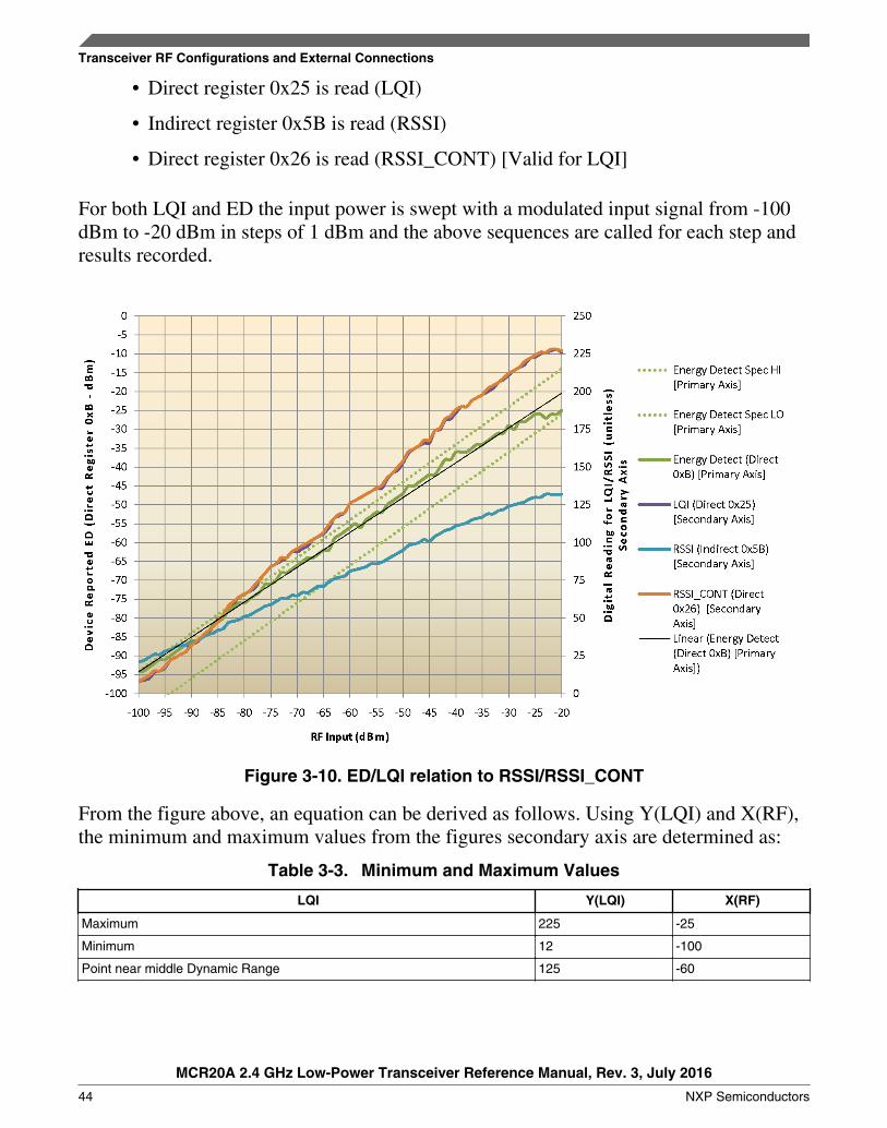
• Direct register 0x25 is read (LQI)
• Indirect register 0x5B is read (RSSI)
• Direct register 0x26 is read (RSSI_CONT) [Valid for LQI]
For both LQI and ED the input power is swept with a modulated input signal from -100dBm to -20 dBm in steps of 1 dBm and the above sequences are called for each step andresults recorded.
Figure 3-10. ED/LQI relation to RSSI/RSSI_CONT
From the figure above, an equation can be derived as follows. Using Y(LQI) and X(RF),the minimum and maximum values from the figures secondary axis are determined as:
Table 3-3. Minimum and Maximum Values
LQI Y(LQI) X(RF)
Maximum 225 -25
Minimum 12 -100
Point near middle Dynamic Range 125 -60
Transceiver RF Configurations and External Connections
MCR20A 2.4 GHz Low-Power Transceiver Reference Manual, Rev. 3, July 2016
44 NXP Semiconductors
Therefore the slope = 2.84 and B = 295.4. So to convert the 8-bit unitless number readfrom direct register 0x25 to an ideal RF equivalent, use the following equation:
RF = (LQI – 295.4) / 2.84
3.10 Timer ResourcesWhen writing software applications, the user should be aware of the set of timerresources available.
3.10.1 Modem Event Timer
The MCR20A transceiver contains an internal Event Timer block whose clock is derivedfrom a programmable prescaler which is driven by the 32 MHz crystal source. The EventTimer consists of the prescaler and a 24-bit counter which increment whenever themodem crystal clock is operating. The Event Timer provides the following functions:
• The 24-bit counter generates “current” system time - The counter runs continuouslywhen the modem is not in a low power mode and provides a local “current” time.The present value can be read from the EVENT_TMR_USB/MSB/LSB registers. Acounter frequency of 250 kHz is used. The counter value is used to generate a timestamp for received frames and is also used for comparison to four differentcomparators that allow up to four different time delays
• Interrupt generation at pre-determined system times - There are four comparatorfunctions that can generate an interrupt to the MCU when the value of thecomparator matches the system counter. These function as timers to generate timedelays or trigger events and can augment the MCU timers for generating time delaysrequired within the 802.15.4 application software
• Exit from Doze Mode at pre-determined system time - Timer comparator Tmr_Cmp2can be used to wake-up the modem from low power Doze Mode
• Latches “timestamp” value during packet reception - With every received frame,there is a timestamp generated and stored in a modem SPI register. The timestamp istaken from the counter when the frame length indicator (FLI) is received
• Initiates timer-triggered sequences - The modem has three basic active modes of RX,TX, and CCA. Each of these sequences can be timer-triggered to become active aftera set delay based on timer comparator Tmr_Cmp2. This feature can be useful forimplementing 802.15.4 application sequences
Chapter 3 System Considerations
MCR20A 2.4 GHz Low-Power Transceiver Reference Manual, Rev. 3, July 2016
NXP Semiconductors 45
3.11 Low Power ConsiderationsMany IEEE 802.15.4 applications such as sensor End Devices are required to be batteryoperated. As expected, long battery life is highly desirable and is very dependent onapplication parameters. Over-the-air operation uses RX, TX, and CCA modes, wherepower is highest. As a result, the time between radio operations should be kept at thelongest possible period that the application will allow.
When designing for low power operation consider:
• The modem and the MCU each have several low power options• The modem is entirely controlled by the MCU; the low power options/combinations
will be determined by MCU programming• The power down control of the modem must be maintained by the MCU in the
MCU's power down configuration• All unused port GPIO must be configured to a known state (preferably output low) to
prevent unwanted leakage current.
Lowest power in a system is more than just putting the modem and/or the MCU in a lowpower mode. The relationship between the functions, the timing between them, and clockmanagement must all be considered. The duty cycle between active operations is alsovery important as it can impact whether sleep operation or active operation will have thebiggest impact over an extended time period.
3.11.1 Low-Power Preamble Search (LPPS)
The Low Power Preamble Search (LPPS) feature of the radio allows the user toeffectively save receiver current while maintaining adequate system performance.Attributes of the the LPPS feature are described as follows:
• When enabling the LPPS feature the demodulator and other sub-sections of thereceiver can be independently duty cycled at 50%.
• The receiver current consumption is reduced approximately 4 mA.• Sensitivity performance decreases slightly due to time delta in the correlator while
searching for an additional s0 before entering normal preamble search.• There is no added cost of using the LPPS feature since no extra components are
required. In fact, enabling LPPS mode all the time has little system design impactand the current savings is 20%.
LPPS Control Register Setup
Low Power Considerations
MCR20A 2.4 GHz Low-Power Transceiver Reference Manual, Rev. 3, July 2016
46 NXP Semiconductors
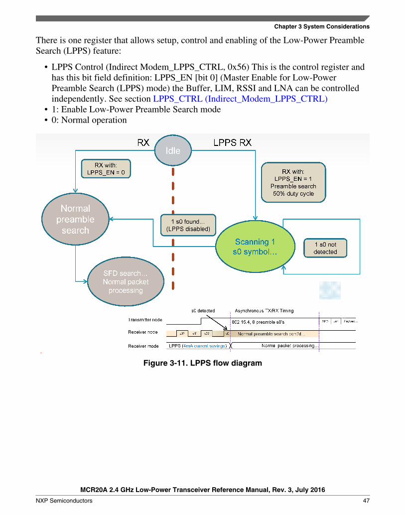
There is one register that allows setup, control and enabling of the Low-Power PreambleSearch (LPPS) feature:
• LPPS Control (Indirect Modem_LPPS_CTRL, 0x56) This is the control register andhas this bit field definition: LPPS_EN [bit 0] (Master Enable for Low-PowerPreamble Search (LPPS) mode) the Buffer, LIM, RSSI and LNA can be controlledindependently. See section LPPS_CTRL (Indirect_Modem_LPPS_CTRL)
• 1: Enable Low-Power Preamble Search mode• 0: Normal operation
Figure 3-11. LPPS flow diagram
Chapter 3 System Considerations
MCR20A 2.4 GHz Low-Power Transceiver Reference Manual, Rev. 3, July 2016
NXP Semiconductors 47
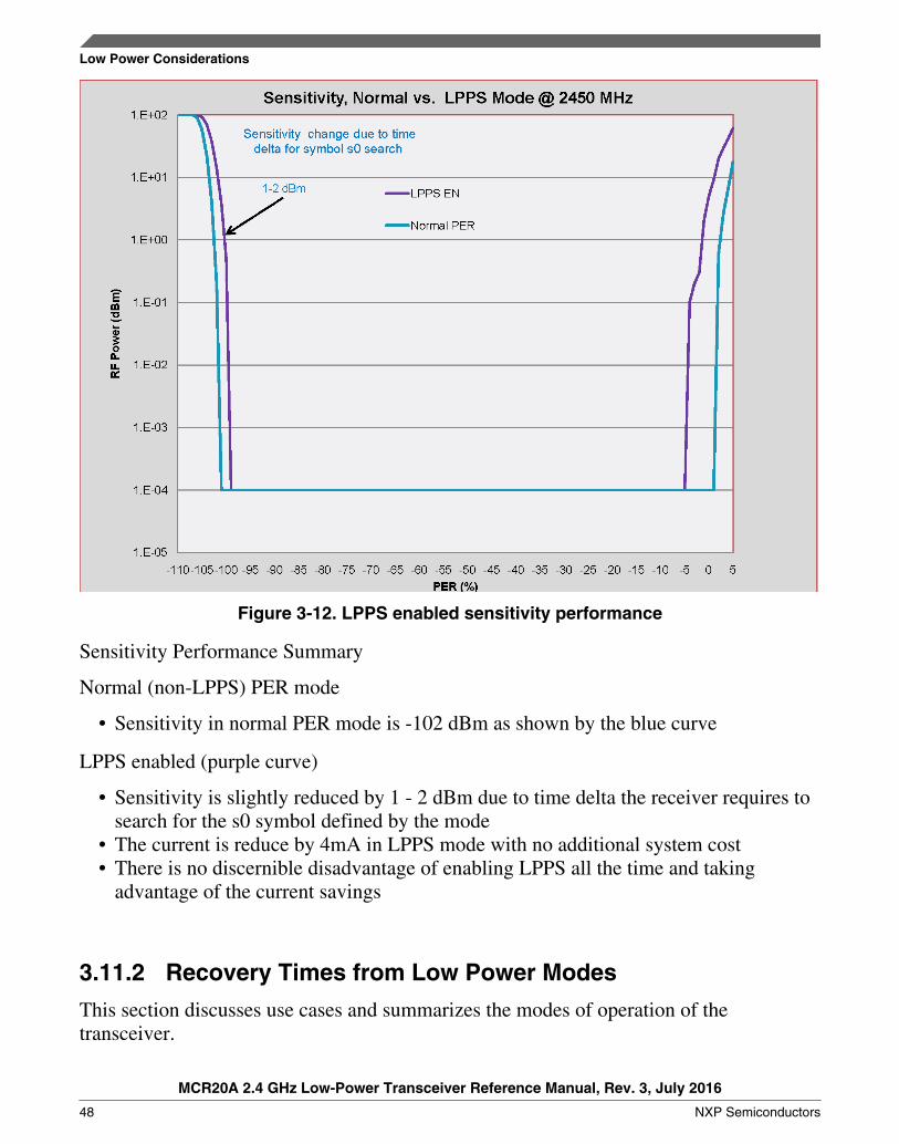
Figure 3-12. LPPS enabled sensitivity performance
Sensitivity Performance Summary
Normal (non-LPPS) PER mode
• Sensitivity in normal PER mode is -102 dBm as shown by the blue curve
LPPS enabled (purple curve)
• Sensitivity is slightly reduced by 1 - 2 dBm due to time delta the receiver requires tosearch for the s0 symbol defined by the mode
• The current is reduce by 4mA in LPPS mode with no additional system cost• There is no discernible disadvantage of enabling LPPS all the time and taking
advantage of the current savings
3.11.2 Recovery Times from Low Power Modes
This section discusses use cases and summarizes the modes of operation of thetransceiver.
Low Power Considerations
MCR20A 2.4 GHz Low-Power Transceiver Reference Manual, Rev. 3, July 2016
48 NXP Semiconductors
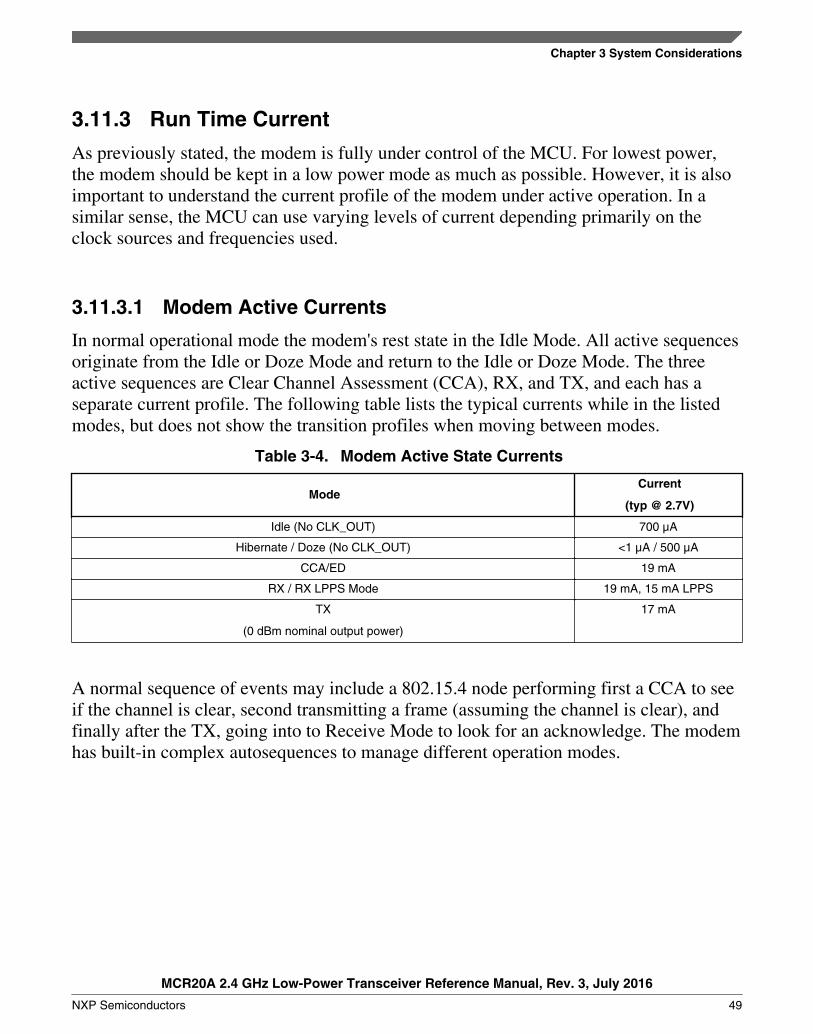
3.11.3 Run Time Current
As previously stated, the modem is fully under control of the MCU. For lowest power,the modem should be kept in a low power mode as much as possible. However, it is alsoimportant to understand the current profile of the modem under active operation. In asimilar sense, the MCU can use varying levels of current depending primarily on theclock sources and frequencies used.
3.11.3.1 Modem Active Currents
In normal operational mode the modem's rest state in the Idle Mode. All active sequencesoriginate from the Idle or Doze Mode and return to the Idle or Doze Mode. The threeactive sequences are Clear Channel Assessment (CCA), RX, and TX, and each has aseparate current profile. The following table lists the typical currents while in the listedmodes, but does not show the transition profiles when moving between modes.
Table 3-4. Modem Active State Currents
ModeCurrent
(typ @ 2.7V)
Idle (No CLK_OUT) 700 µA
Hibernate / Doze (No CLK_OUT) <1 µA / 500 µA
CCA/ED 19 mA
RX / RX LPPS Mode 19 mA, 15 mA LPPS
TX
(0 dBm nominal output power)
17 mA
A normal sequence of events may include a 802.15.4 node performing first a CCA to seeif the channel is clear, second transmitting a frame (assuming the channel is clear), andfinally after the TX, going into to Receive Mode to look for an acknowledge. The modemhas built-in complex autosequences to manage different operation modes.
Chapter 3 System Considerations
MCR20A 2.4 GHz Low-Power Transceiver Reference Manual, Rev. 3, July 2016
NXP Semiconductors 49

Low Power Considerations
MCR20A 2.4 GHz Low-Power Transceiver Reference Manual, Rev. 3, July 2016
50 NXP Semiconductors

Chapter 4Modem: Modes of Operation
4.1 Power Management OverviewThe power management structure provides the biasing and the framework to powermanage the MCR20A.
The power management includes:
• A 1.8V digital regulator with POR
• A 1.8V analog regulator
• Biasing block
The supply strategy block diagram is provided in the following figure.
MCR20A 2.4 GHz Low-Power Transceiver Reference Manual, Rev. 3, July 2016
NXP Semiconductors 51
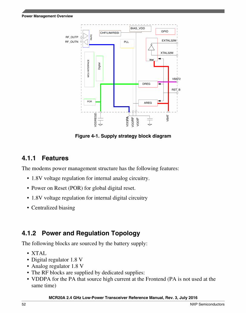
DREG
AREG
RF_OUTP
RF_OUTN
CHF/LIM/RSSI
BIAS_VDDGPIO
PLL
PA/F
E
EXTAL32M
XTAL32M
Xtal
MC
U IN
TE
RFA
CE
Dig
ital
POR
VBAT2
RST_B
VD
DR
EG
D
VD
DPA
VD
DR
F
VD
DIF VB
AT
Figure 4-1. Supply strategy block diagram
4.1.1 Features
The modems power management structure has the following features:
• 1.8V voltage regulation for internal analog circuitry.
• Power on Reset (POR) for global digital reset.
• 1.8V voltage regulation for internal digital circuitry
• Centralized biasing
4.1.2 Power and Regulation Topology
The following blocks are sourced by the battery supply:
• XTAL• Digital regulator 1.8 V• Analog regulator 1.8 V• The RF blocks are supplied by dedicated supplies:• VDDPA for the PA that source high current at the Frontend (PA is not used at the
same time)
Power Management Overview
MCR20A 2.4 GHz Low-Power Transceiver Reference Manual, Rev. 3, July 2016
52 NXP Semiconductors
• VDDRF for the PLL block (mainly VCO), clean supply regulated by the LDOdirectly
• VDDIF for the other analog blocks and also used potentially by the XOR.
VDDPA and VDDIF are connected externally such that decoupling between supplies iseasy
4.1.3 Digital Regulator and POR
The digital regulator provides the 1.8 V supply to the digital logic. It is always turned onwhen the RST_B pin has been released. For VDDREGD, the external decouplingcapacitor is in the range of 220 nF and 470 nF. As the figure below shows, theVDDREGD supply is decoupled externally. The digital regulator includes three modes ofoperation:
• Off mode - controlled by the active low RST_B pin, and active when reset is active
• On mode with maximum current capability - required in RUN mode and duringstartup
• Low power mode (in LP/HB and DOZE) - The current capability in this mode islimited but retains register contents and SPI functionality. The current consumptionis max 300 µA.
POR block provides reset if VBAT is low (</=1.4 V). POR comes out of reset if VBATis high (>/=1.65 V). The POR is used to hold the digital logic in reset and then release thextal oscillator when the power is going up.
Note• The POR is disabled during loose mode. (See "Modes and
start up process" Table).
• There is no battery monitoring
4.1.4 Analog Regulator (AREG)
The analog regulator is a low drop linear regulator that regulates to 1.8 V typical from thebattery voltage 3.6 V-1.8 V. When the battery is low the regulated supply VDDRFfollows the battery voltage (max 150 mV drop). This LDO provides the supply to the RF
Chapter 4 Modem: Modes of Operation
MCR20A 2.4 GHz Low-Power Transceiver Reference Manual, Rev. 3, July 2016
NXP Semiconductors 53
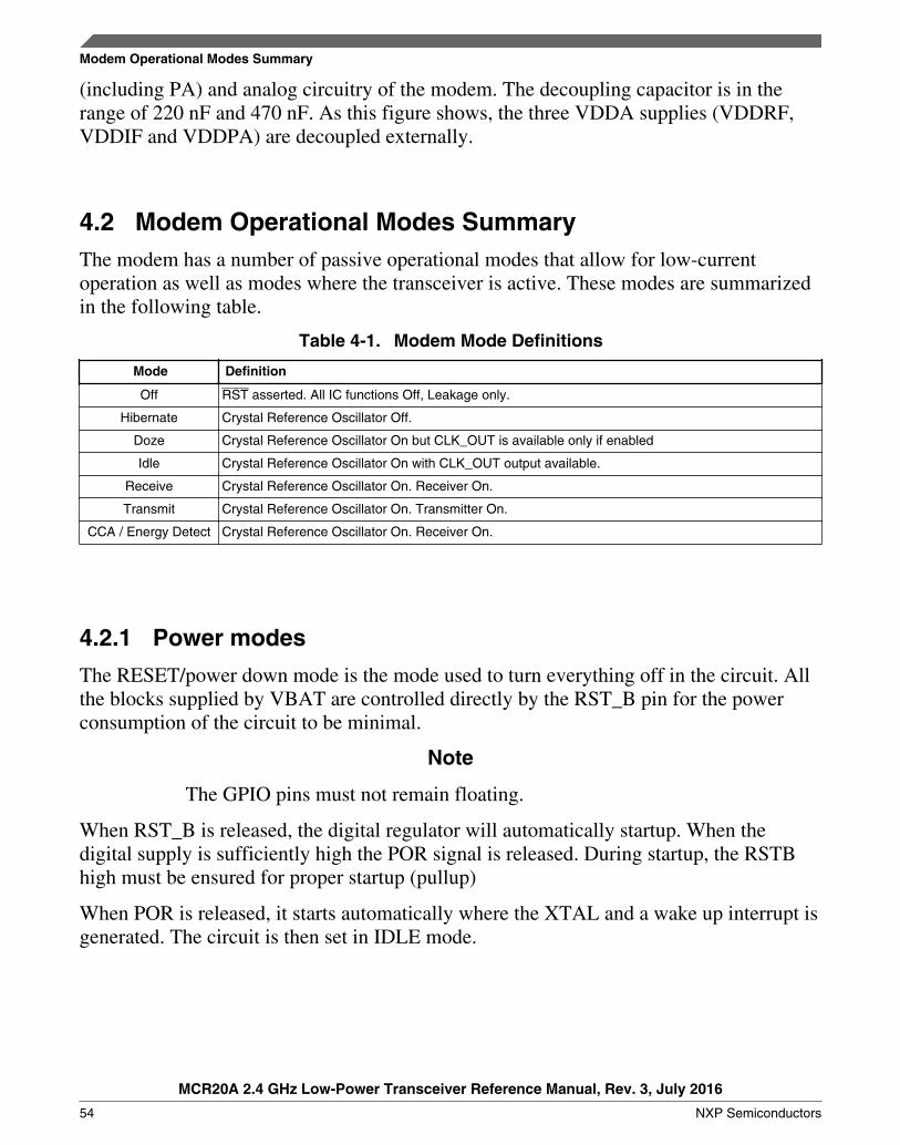
(including PA) and analog circuitry of the modem. The decoupling capacitor is in therange of 220 nF and 470 nF. As this figure shows, the three VDDA supplies (VDDRF,VDDIF and VDDPA) are decoupled externally.
4.2 Modem Operational Modes SummaryThe modem has a number of passive operational modes that allow for low-currentoperation as well as modes where the transceiver is active. These modes are summarizedin the following table.
Table 4-1. Modem Mode Definitions
Mode Definition
Off RST asserted. All IC functions Off, Leakage only.
Hibernate Crystal Reference Oscillator Off.
Doze Crystal Reference Oscillator On but CLK_OUT is available only if enabled
Idle Crystal Reference Oscillator On with CLK_OUT output available.
Receive Crystal Reference Oscillator On. Receiver On.
Transmit Crystal Reference Oscillator On. Transmitter On.
CCA / Energy Detect Crystal Reference Oscillator On. Receiver On.
4.2.1 Power modes
The RESET/power down mode is the mode used to turn everything off in the circuit. Allthe blocks supplied by VBAT are controlled directly by the RST_B pin for the powerconsumption of the circuit to be minimal.
Note
The GPIO pins must not remain floating.
When RST_B is released, the digital regulator will automatically startup. When thedigital supply is sufficiently high the POR signal is released. During startup, the RSTBhigh must be ensured for proper startup (pullup)
When POR is released, it starts automatically where the XTAL and a wake up interrupt isgenerated. The circuit is then set in IDLE mode.
Modem Operational Modes Summary
MCR20A 2.4 GHz Low-Power Transceiver Reference Manual, Rev. 3, July 2016
54 NXP Semiconductors
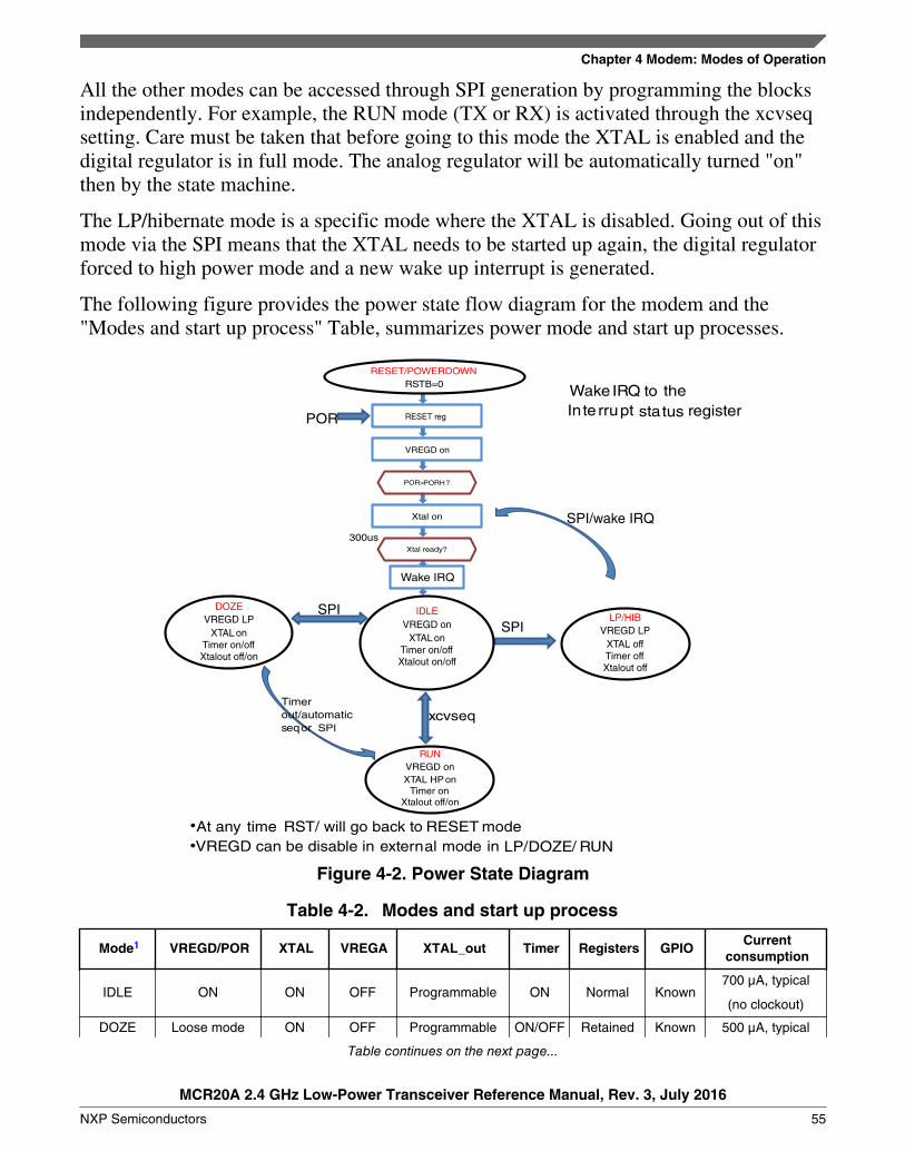
All the other modes can be accessed through SPI generation by programming the blocksindependently. For example, the RUN mode (TX or RX) is activated through the xcvseqsetting. Care must be taken that before going to this mode the XTAL is enabled and thedigital regulator is in full mode. The analog regulator will be automatically turned "on"then by the state machine.
The LP/hibernate mode is a specific mode where the XTAL is disabled. Going out of thismode via the SPI means that the XTAL needs to be started up again, the digital regulatorforced to high power mode and a new wake up interrupt is generated.
The following figure provides the power state flow diagram for the modem and the"Modes and start up process" Table, summarizes power mode and start up processes.
RESET/POWERDOWNRSTB=0
RESET reg
VREGD on
POR>PORH?
Xtal on
Xtal ready?
Wake IRQ
POR
Wake IRQ to theInte rrupt status register
SPISPI
SPI/wake IRQ
DOZEVREGD LP
XTAL onTimer on/offXtalout off/on
IDLEVREGD on
XTAL onTimer on/offXtalout on/off
LP/HIBVREGD LP
XTAL offTimer offXtalout off
Timerout/automaticseq or SPI
xcvseq
RUNVREGD onXTAL HP on
Timer onXtalout off/on
300us
At any time RST/ will go back to RESET modeVREGD can be disable in external mode in LP/DOZE/ RUN
Figure 4-2. Power State Diagram
Table 4-2. Modes and start up process
Mode1 VREGD/POR XTAL VREGA XTAL_out Timer Registers GPIOCurrent
consumption
IDLE ON ON OFF Programmable ON Normal Known700 µA, typical
(no clockout)
DOZE Loose mode ON OFF Programmable ON/OFF Retained Known 500 µA, typical
Table continues on the next page...
Chapter 4 Modem: Modes of Operation
MCR20A 2.4 GHz Low-Power Transceiver Reference Manual, Rev. 3, July 2016
NXP Semiconductors 55
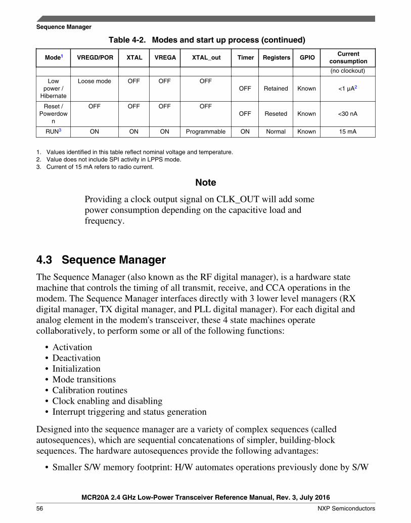
Table 4-2. Modes and start up process (continued)
Mode1 VREGD/POR XTAL VREGA XTAL_out Timer Registers GPIOCurrent
consumption
(no clockout)
Lowpower /
Hibernate
Loose mode OFF OFF OFFOFF Retained Known <1 µA2
Reset /Powerdow
n
OFF OFF OFF OFFOFF Reseted Known <30 nA
RUN3 ON ON ON Programmable ON Normal Known 15 mA
1. Values identified in this table reflect nominal voltage and temperature.2. Value does not include SPI activity in LPPS mode.3. Current of 15 mA refers to radio current.
Note
Providing a clock output signal on CLK_OUT will add somepower consumption depending on the capacitive load andfrequency.
4.3 Sequence ManagerThe Sequence Manager (also known as the RF digital manager), is a hardware statemachine that controls the timing of all transmit, receive, and CCA operations in themodem. The Sequence Manager interfaces directly with 3 lower level managers (RXdigital manager, TX digital manager, and PLL digital manager). For each digital andanalog element in the modem's transceiver, these 4 state machines operatecollaboratively, to perform some or all of the following functions:
• Activation• Deactivation• Initialization• Mode transitions• Calibration routines• Clock enabling and disabling• Interrupt triggering and status generation
Designed into the sequence manager are a variety of complex sequences (calledautosequences), which are sequential concatenations of simpler, building-blocksequences. The hardware autosequences provide the following advantages:
• Smaller S/W memory footprint: H/W automates operations previously done by S/W
Sequence Manager
MCR20A 2.4 GHz Low-Power Transceiver Reference Manual, Rev. 3, July 2016
56 NXP Semiconductors
• Increases MCU sleep times, reducing current consumption• Handles timing-critical sequences (rx-to-tx), e.g., data-polling, not possible in S/W
Sequences can be initiated by software directly, or alternatively, can be initiatedautomatically at the expiration of a hardware timer. The general parameters of thesequences can be programmed by software prior to initiating the sequences. Suchparameters allow software to select:
• Whether CCA is required ahead of a transmit sequence• Whether an automatic Ack frame should be transmitted after a receive sequence• Slotted vs. unslotted mode• Type of CCA (e.g., Energy Detect, CCA mode 2)• Whether the device is a PAN Coordinator or not• Whether the device resides on 2 networks simultaneously (Dual PAN mode)
The modem's Sequence Manager also includes support for Dual PAN mode, and ActivePromiscuous mode.
4.3.1 Modem Sequence Manager Operation
The Sequence Manager controls, coordinates, and automates all transceiver sequenceswithin the modem. Software selects the desired sequence, sets the general parameters,and (optionally) configures a hardware timer to trigger the sequence at a precise time inthe future. Subsequently, the MCU can enter a low-power state, or tend to other activities,while the sequence manager state machine conducts the programmed transceiveroperations. When the sequence completes, an interrupt alerts the MCU. At this point theMCU can check the completion status of the sequence, download received data from thepacket buffer, and then prepare the next sequence.
Sequences can be simple transceiver operations. For example, transmit one frame, or,perform a CCA on a channel. Alternatively, the sequence manager supports complexsequences, which use simple operations as building blocks, strung together in a back-to-back fashion, with precise timing intervals between operations. For example, a “TR”sequence calls for a transmit frame followed by a receive frame. For complex sequences,interrupts can optionally be generated at the completion of each stage of the sequence,providing greater visibility for the MCU into the timeline of the sequence. Software candetermine the precise state of the sequence manager state machine at any time. Softwarecan opt to abort a sequence at any time; when this happens, the sequence manager willreturn to its IDLE state in an orderly fashion.
The sequence manager is responsible for the implementation of the Wireless PhysicalLayer (PHY) specifications described in the IEEE 802.15.4 standard, in the modem. Thisis accomplished by activating and deactivating the key digital and analog elements in the
Chapter 4 Modem: Modes of Operation
MCR20A 2.4 GHz Low-Power Transceiver Reference Manual, Rev. 3, July 2016
NXP Semiconductors 57
transmit or receive chain, at precisely the right times, and for precisely the rightdurations. Most of the low-level timing parameters are hardwired within the statemachine, and thus are not programmable. The time resolution of the sequence manager is2 μs (1/8 of a transmitted symbol), so this is the granularity of the individual steps. Thehigher-level timing parameters, such as the interval between operations in a complexsequence, are largely programmable, except for those defined as constants in the IEEE802.15.4 standard.
4.3.2 Functional Description
This section describes the supported sequences in more detail. All sequences can beinitiated by software directly (instantaneously) by writing the desired sequence to theXCVSEQ register, with the TMRTRIGEN bit deasserted. Alternatively, software canschedule the initiation of a sequence at a precise time in the future, by programming thedesired start time into the TC2 timer compare register, and setting the TMRTRIGEN bit.The XCVSEQ register field is writable and readable, so software can read this register todetermine which sequence it had programmed earlier. After the sequence completes(SEQIRQ interrupt), software must set the XCVSEQ to IDLE (0x0), before initiating anew sequence. This prevents the undesired, inadvertent re-triggering of the sequencemanager on the next TC2 match. If the sequence-complete interrupt (SEQIRQ) ismasked, software can determine when the sequence is complete by polling theSEQ_STATE register, until it returns to idle (0x0). While a sequence is ongoing,software can abort the sequence at any time by writing IDLE (0x0) to XCVSEQ; thesequence manager state machine will respond with an orderly return to the SEQ_IDLEstate, and a SEQIRQ will be generated. While a sequence is underway, software shouldnot attempt to change XCVSEQ (other than aborting the sequence as previouslydescribed); the sequence manager will ignore all mid-sequence attempts to changeXCVSEQ. As mentioned previously, software must write the IDLE value to XCVSEQbefore changing sequences.
The supported sequences are shown in the following table.
Table 4-3. Transceiver supported sequences
XCVSEQ Sequence Description
0 I Idle
1 R Receive Sequence - conditionallyfollowed by a TxAck
2 T Transmit Sequence
3 C Standalone CCA
Table continues on the next page...
Sequence Manager
MCR20A 2.4 GHz Low-Power Transceiver Reference Manual, Rev. 3, July 2016
58 NXP Semiconductors
Table 4-3. Transceiver supported sequences (continued)
XCVSEQ Sequence Description
4 TR Transmit /Receive Sequence - transmitunconditionally followed by either an R
or RxAck
5 CCCA Continuous CCA - sequence completeswhen channel is idle
6 Reserved
7 Reserved
All sequences can be aborted by a PLL unlock detection. In the modem, this is referred toas PLL unlock. The unlock detection is qualified by the sequence manager; in otherwords, an unlock detection during the early stages of the PLL warmup is expected, and isnot allowed to abort the sequence at that point. The primary rationale for the PLL unlockabort, is to prevent transmission on an incorrect, or unstable, frequency during a transmitoperation, or to increase battery life by not prolonging a receive or CCA operation that isbound to fail. Software can disable the PLL unlock auto-abort altogether by asserting thePLL_ABORT_OVERRIDE bit.
Supported Sequences
4.3.2.1.1 Sequence (Idle)
When the IDLE value is written to XCVSEQ, the sequence manager goes to itsSEQ_IDLE state. If not already in SEQ_IDLE, the sequence manager executes an orderlywarmdown to return to SEQ_IDLE. A SEQIRQ interrupt is then issued. Writing IDLEvalue to XCVSEQ is the proper way to abort a sequence.
4.3.2.1.2 Sequence R (Receive)
Sequence R is the basic receive sequence. Sequence R can be used to receive all types of802.15.4 PHY- and MAC-compliant frames, including reserved frame types. However,reception of Acknowledge frames is not recommended using Sequence R. This is becausereception of an Acknowledge frame, usually follows a transmitted frame, with adesignated Sequence Number, so that the received Acknowledge frame can be verifiedfor the matching Sequence Number. In a standalone Sequence R, there is no SequenceNumber to verify against, so any Acknowledge frame is merely transferred to the PacketBuffer. (Note: the appropriate way to receive Acknowledge frames is with Sequence TR,with the RXACKRQD bit asserted). Using Sequence R, all frames that pass frame-filtering rules and CRC check, are transferred to the Packet Buffer.
The basic execution of a successful Sequence R is as follows:
4.3.2.1
Chapter 4 Modem: Modes of Operation
MCR20A 2.4 GHz Low-Power Transceiver Reference Manual, Rev. 3, July 2016
NXP Semiconductors 59
• MCU writes TC2 compare value to the desired initiation time, and setsTMRTRIGEN (optional)
• MCU writes XCVSEQ=R• Wait for TC2 match (if TMRTRIGEN=1)• SEQ_MGR executes RxWarmup• Preamble Detected• SFD Detected• FrameLength octet received, transferred to Packet Buffer• N additional octets received (N = FrameLength), transferred to Packet Buffer. Note if
(FrameLength > 127), then N = 127.• If frame-filtering rules and CRC check pass
• RXIRQ interrupt issued• SEQ_MGR executes RxWarmdown• If received Frame Control Field indicates AckRequest=1
• SEQ_MGR executes TxWarmup• an Ack frame is transmitted using the received Sequence Number• SEQ_MGR executes TxWarmdown
• SEQIRQ interrupt issued
When Sequence R is initiated, the sequence manager warms up the receiver (analog anddigital elements). This process takes 144 μs. From this point forward, timer TMR3 can beenabled as a “bracketing” timer (software option). If a TMR3 timer match occurs, andsoftware has asserted the TC3TMOUT bit, the sequence manager will warm down thereceiver and return to SEQ_IDLE state. Assuming no TMR3 timeout, reception proceedsin preamble-search mode. After a preamble is detected, reception continues in SFD-search mode. At this point, the sequence manager’s slot timer is activated. This isbecause a slotted “transmit acknowledge” frame (TxAck) may be required later in thissequence. The slot timer is loaded with the following value (in μs):
Slot Timer Preload = 160 + TXWARMUPTIME + (2*ACKDELAY).
The 160 term arises because, at the point of SFD detect, we are exactly 10 symbols intothe backoff slot, and the symbol period is 16 μs. (The slot timer timebase is actually 2 μs,half the time-resolution of the equation shown above). The slot timer will count up andeventually rollover at 319, to 0. (There are 320 μs in a backoff slot). The receiver receivesthe next octet (FrameLength). Starting with this octet, and continuing through theremainder of the frame, each octet that is received is transferred to Packet Buffer. Aftereach octet is transferred to Packet Buffer, the Packet Buffer address is incremented by 1.The next 2 octets (Frame Control Field) are then received, which are parsed to obtain theAckRequest field, and the FrameVersion field. The next octet is then received(SequenceNumber), and stored. The remainder of the frame, determined byFrameLength, is then received. As the octets are received, the packet data is parsed andsubjected to packet-filtering rules. If any of the packet-filtering rules fail, or if the CRC
Supported Sequences
MCR20A 2.4 GHz Low-Power Transceiver Reference Manual, Rev. 3, July 2016
60 NXP Semiconductors

check on the FCS field fails, the sequence manager will return the receiver to preamble-search mode, after the last octet has been received and transferred to Packet Buffer.Assuming the packet-filtering rules and CRC pass, an interrupt (RXIRQ) is issued to theMCU. At this point, the sequence manager must determine whether a TxAck is required.A TxAck is required if the following 3 conditions are all met:
• AUTOACK=1 (register bit)• PROMISCUOUS=0 (register bit)• The received FrameControlField has AckRequest=1
If these conditions are met, and SLOTTED mode is not in effect, the sequence managerloads its TxAck timer with the following value (in μs):
TxAck Timer Preload = 192 - TXWARMUPTIME - 2*ACKDELAY +16*ACKPOSTPONE. Note: ACKPOSTPONE is not supported in the modem and ishardwired to 0.
The 192 μs is the non-slotted RX-to-TX turnaround requirement in the 802.15.4 standard.The TXWARMUPTIME takes into account the fact that the TxAck timer must expireearly for the Tx warmup to be complete at exactly the 192 μs point. The ACKDELAY isa signed, fine-tune adjustment to the TxAck transmission time (± 62 µs), and theACKPOSTPONE allows the TxAck to be delayed an additional 255 symbols, ifnecessary.
If SLOTTED mode is in effect, the slot timer was previously loaded (at SFD detect), butthe sequence manager needs to determine how much time is left in the current backoffslot. If less than 192 μs remain, the sequence manager must wait an additional backoffslot before initiating the Ack transmission. So it sets a flag indicating it must allow theslot counter to rollover an additional iteration.
Finally, at TxAck timer expiration (in non-SLOTTED mode), or at the qualified rolloverof the slot timer (in SLOTTED mode), a Tx warmup is initiated. The conclusion of theTx warmup will coincide precisely with a backoff slot boundary if SLOTTED mode is ineffect. The sequence manager will then initiate the transmission of the Ack frame. Theentire Ack frame will be built up by hardware; the Packet Buffer is not used for the auto-TxAck feature. The hardware will insert the following parameters into the Ack frame’sFrame Control Field:
Table 4-4. Frame Control Field for Hardware-generated Auto-TxAck Frame
FCF Field Value
FrameType Acknowledge
SecurityEnabled 0
Table continues on the next page...
Chapter 4 Modem: Modes of Operation
MCR20A 2.4 GHz Low-Power Transceiver Reference Manual, Rev. 3, July 2016
NXP Semiconductors 61

Table 4-4. Frame Control Field for Hardware-generated Auto-TxAck Frame (continued)
FCF Field Value
FramePending If SRCADDR_EN=1, FramePending gets the value of FramePendingFlag from SourceAddress Matching accelerator hardware. If SRCADDR_EN=0, FramePending gets thevalue of ACK_FRM_PND.
AckRequest 0
PanIDCompression 0
Reserved (bits 7-9) 000
DstAddrMode 0
FrameVersion copy FrameVersion from the previously-received frame
SrcAddrMode 0
The Sequence Number for the Ack packet, will be the Sequence Number obtained fromthe previously received frame.
After the Ack frame has been transmitted, the sequence manager will issue a TXIRQinterrupt, and then perform a Tx warmdown. Finally, a SEQIRQ interrupt will be issued,and the sequence manager returns to SEQ_IDLE state.
4.3.2.1.3 Sequence T (Transmit)
Sequence T is the basic, standalone transmit sequence. Sequence T can be used totransmit all types of 802.15.4 PHY- and MAC-compliant frames. However, transmissionof Acknowledge frames is not recommended using Sequence T. This is becausetransmission of an Acknowledge frame, usually follows a received frame, with adesignated Sequence Number. The sequence manager automates the transmission of anAck frame that follows a received frame, using Sequence R with the AUTOACK bitasserted. This is the recommended method for transmitting an Ack frame. This isespecially beneficial, because the transmitted Ack frame octets are generated byhardware, and so no setup of a transmit packet in Packet Buffer, is required. However,sequence manager hardware does not prohibit Ack frames using Sequence T.
Sequence T allows for the insertion of 1 or 2 CCA (clear channel assessment)measurements prior to transmission, to ensure that the selected channel is idle. The CCA-before-TX feature is governed by two register bits, CCABFRTX and SLOTTED. AllCCA measurements must indicate channel-idle, in order for the sequence manager toproceed to transmission; if the channel is determined by CCA to be busy, the sequencemanager will terminate the sequence without a transmission. The number of CCAmeasurements attempted by the sequence manager, and the timing of the measurements,is shown in the following table.
Supported Sequences
MCR20A 2.4 GHz Low-Power Transceiver Reference Manual, Rev. 3, July 2016
62 NXP Semiconductors
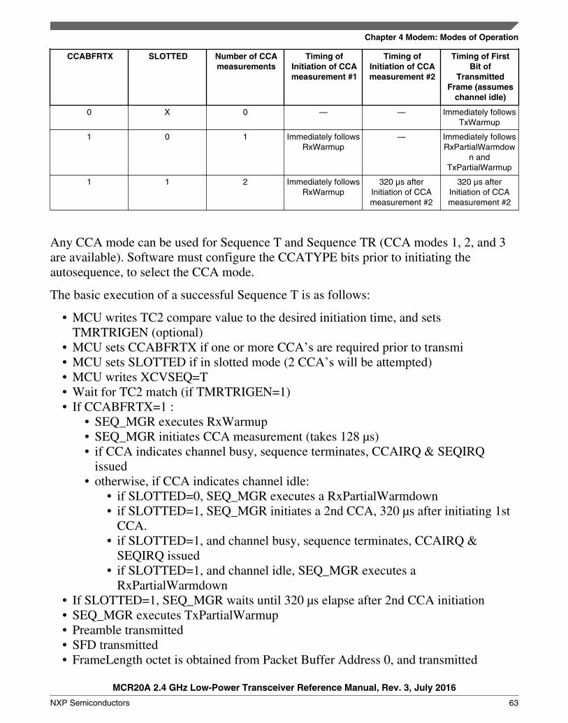
CCABFRTX SLOTTED Number of CCAmeasurements
Timing ofInitiation of CCAmeasurement #1
Timing ofInitiation of CCAmeasurement #2
Timing of FirstBit of
TransmittedFrame (assumes
channel idle)
0 X 0 — — Immediately followsTxWarmup
1 0 1 Immediately followsRxWarmup
— Immediately followsRxPartialWarmdow
n andTxPartialWarmup
1 1 2 Immediately followsRxWarmup
320 µs afterInitiation of CCAmeasurement #2
320 µs afterInitiation of CCAmeasurement #2
Any CCA mode can be used for Sequence T and Sequence TR (CCA modes 1, 2, and 3are available). Software must configure the CCATYPE bits prior to initiating theautosequence, to select the CCA mode.
The basic execution of a successful Sequence T is as follows:
• MCU writes TC2 compare value to the desired initiation time, and setsTMRTRIGEN (optional)
• MCU sets CCABFRTX if one or more CCA’s are required prior to transmi• MCU sets SLOTTED if in slotted mode (2 CCA’s will be attempted)• MCU writes XCVSEQ=T• Wait for TC2 match (if TMRTRIGEN=1)• If CCABFRTX=1 :
• SEQ_MGR executes RxWarmup• SEQ_MGR initiates CCA measurement (takes 128 µs)• if CCA indicates channel busy, sequence terminates, CCAIRQ & SEQIRQ
issued• otherwise, if CCA indicates channel idle:
• if SLOTTED=0, SEQ_MGR executes a RxPartialWarmdown• if SLOTTED=1, SEQ_MGR initiates a 2nd CCA, 320 µs after initiating 1st
CCA.• if SLOTTED=1, and channel busy, sequence terminates, CCAIRQ &
SEQIRQ issued• if SLOTTED=1, and channel idle, SEQ_MGR executes a
RxPartialWarmdown• If SLOTTED=1, SEQ_MGR waits until 320 µs elapse after 2nd CCA initiation• SEQ_MGR executes TxPartialWarmup• Preamble transmitted• SFD transmitted• FrameLength octet is obtained from Packet Buffer Address 0, and transmitted
Chapter 4 Modem: Modes of Operation
MCR20A 2.4 GHz Low-Power Transceiver Reference Manual, Rev. 3, July 2016
NXP Semiconductors 63
• CRC engine is reset• N additional octets are obtained from Packet Buffer and transmitted (N =
FrameLength - 2)• Each octet that is transmitted, is shifted through the CRC engine• After Nth octet transmitted, FCS is available from CRC engine.• FCS lower octet transmitted• FCS upper octet transmitted• SEQ_MGR issues TXIRQ• SEQ_MGR executes TxWarmdown• SEQ_MGR issues SEQIRQ
When Sequence T is initiated, the sequence manager first must determine whether one ormore CCA measurements are required. If CCABFRTX bit is asserted, the sequencemanager warms up the receiver (analog and digital elements). This process takes 144 µs.Immediately after the conclusion of the warmup, a CCA measurement is initiated. TheCCA measurement takes 128 ms. If CCA indicates the channel is busy, the sequencemanager warms down the receiver, issues CCAIRQ and SEQIRQ interrupts, andterminates the sequence. If, however, CCA indicates the channel is idle, the sequencemanager inspects the SLOTTED bit to determine what to do next. If the SLOTTED bit isclear, the sequence manager issues a CCAIRQ interrupt, and then executes a partialwarmdown of the receiver. If, however, the SLOTTED bit is set, the sequence managerdoes not issue a CCAIRQ interrupt; instead, the sequence manager initiates a secondCCA measurement, precisely 320 µs after the initiation of the first CCA. This 320 µsinterval is timed by the slot timer, which had been preloaded with 320 µs at the instantthat Rx warmup was complete. At the conclusion of the second CCA, the sequencemanager issues a CCAIRQ. If the second CCA indicates the channel is busy, thesequence manager warms down the receiver, issues a SEQIRQ interrupt, and terminatesthe sequence. If, however, CCA indicates the channel is idle, the sequence managerexecutes a warmdown of the receiver. Prior to executing the warmdown, the sequencemanager reloads the slot timer, in order to precisely schedule the ensuing transmission.This time, the slot timer is loaded with a smaller value, in order to account for the factthat the timer must expire early in order to trigger the Tx warmup, which must completeat precisely the next backoff slot boundary. Thus, this time the slot timer is preloadedwith:
Slot Timer Preload = 320 - TXWARMUPTIME + (2*TXDELAY).
The 320 µs is the duration of the backoff slot. The TXWARMUPTIME takes intoaccount the fact that the TxAck timer must expire early for the Tx warmup to becomplete at exactly the 320 µs point. The TXDELAY is a signed, fine-tune adjustment tothe TxAck transmission time (± 62 µs).
Supported Sequences
MCR20A 2.4 GHz Low-Power Transceiver Reference Manual, Rev. 3, July 2016
64 NXP Semiconductors

If the SLOTTED bit is asserted, after the slot timer expires, the sequence managerexecutes a Tx warmup. The conclusion of this warmup coincides with the backoff slotboundary. If the SLOTTED bit is deasserted, the sequence manager does not wait for theslot timer, and instead executes the partial Tx warmup immediately after the partial Rxwarmdown.
At this point, the sequence manager begins the transmit operation. The preamble andSFD are transmitted first. The preamble and SFD octets are generated by hardware, andare not included in the Packet Buffer. Then, the FrameLength octet is obtained from thePacket Buffer (address 0), and the buffer address pointer is incremented by one. TheFrameLength octet is transmitted. The CRC engine is reset at this point. TheFrameLength octet is used to determine how many more octets remain in the PacketBuffer. The number of remaining octets is:
Number of octets remaining in Tx buffer = FrameLength - 2
This is because the final 2 octets of the transmit frame constitute the FCS (Frame CheckSequence), and this value is hardware-computed. Thus, FCS is not part of the Tx buffer.Each of the octets in the Tx buffer is transmitted, and simultaneously shifted throughCRC, to generate the FCS field. After the Tx buffer is drained and all of its octetstransmitted, the 2 FCS octets are transmitted, starting with the least significant octet. Atthis point, the transmit operation is complete. The sequence manager issues a TXIRQinterrupt. The sequence manager then executes a complete Tx warmdown, and follows upwith a SEQIRQ interrupt. The sequence manager returns to SEQ_IDLE state.
4.3.2.1.4 Sequence C (Standalone CCA)
Sequence C is the standalone CCA sequence. During Sequence C, the sequence managerexecutes a Clear Channel Assessment (CCA). The result of the CCA measurement isreported back to software in the CCA bit of the IRQSTS2 Register. The CCA bitindicates either a busy channel (1), or an idle channel (0).
The basic execution of a Sequence C is as follows:
• MCU writes TC2 compare value to the desired initiation time, and setsTMRTRIGEN (optional)
• MCU writes XCVSEQ=C• Wait for TC2 match (if TMRTRIGEN=1)• SEQ_MGR asserts one of {cca1_en, cca2_en, cca3_en, ed_en} to CCA_DIG• SEQ_MGR executes RxWarmup• SEQ_MGR waits an additional 26 µs for RSSI/AGC settling• SEQ_MGR initiates CCA measurement by asserting rx_cca_en to CCA_DIG• SEQ_MGR waits for CCA to complete• CCA bit is set to the CCA status (1=busy 0=idle)
Chapter 4 Modem: Modes of Operation
MCR20A 2.4 GHz Low-Power Transceiver Reference Manual, Rev. 3, July 2016
NXP Semiconductors 65
• CCAIRQ interrupt issued• SEQ_MGR executes RxWarmdown• SEQIRQ interrupt issued
When Sequence C is initiated, the sequence manager asserts one of 4 control signals toCCA_DIG, based on which CCA or ED mode is programmed into CCATYPE. Themapping of CCATYPE to control signal is shown in the following table:
CCATYPE CCA Control Signal
00 ed_en
01 cca1_en
10 cca2_en
11 cca3_en
The asserted control signal will remain asserted for the duration of the Sequence C. Thesequence manager warms up the receiver (analog and digital elements). This processtakes 144 µs. The TC3 “bracketing” timer has no effect on the sequence manager duringSequence C, so it cannot abort the sequence. At the completion of the warmup, thesequence manager initiates the CCA by asserting the rx_cca_en signal to CCA_DIG.While CCA is enabled, the CCA_DIG measures and averages the energy or signal on thechannel. At the completion of the CCA process, the CCA bit is set to the status of thechannel (idle or busy). The CCAIRQ is issued, the receiver is warmed down, theSEQIRQ is issued, and the sequence manager returns to SEQ_IDLE state.
Any CCATYPE setting may be used for Sequence C.
4.3.2.1.5 Sequence TR (Transmit/Receive)
Sequence TR is a combination Transmit/Receive sequence. The sequence is executed as aconcatenation of 1 transmit operation followed by 1 receive operation, with a minimumTX-to-RX turnaround time in between. There are 2 permutations of Sequence TR,depending on the RXACKRQD bit. For both permutations, the Sequence T thatconstitutes the first half of a Sequence TR, is identical to the standalone Sequence T(XCVSEQ=2). This means that the transmit operation can be slotted or unslotted, and canbe preceded by 1 or 2 CCA measurements, depending on the state of the CCABFRTXand SLOTTED bits.
If RXACKRQD=0, then Sequence TR is executed as a Sequence T followed by aSequence R, with a minimum TX-to-RX turnaround time in between. The Sequence R,which constitutes the second half of the Sequence TR, is identical to the standaloneSequence R (XCVSEQ=1). This means that the receive operation can be followed by an
Supported Sequences
MCR20A 2.4 GHz Low-Power Transceiver Reference Manual, Rev. 3, July 2016
66 NXP Semiconductors

automatic, hardware-generated transmit Acknowledge frame, if all the necessaryconditions are met. As with basic Sequence R, data for a successful receive operation isalways transferred to Packet Buffer.
If RXACKRQD=1, then Sequence TR is executed as a Sequence T followed by aReceive-Acknowledge-Only frame. This type of receive operation is special, and not thesame as a standalone Sequence R. The Ack-only receive operation filters all incomingframes, looking only for an Acknowledge frame whose Sequence Number matches theSequence Number that was transmitted in the Sequence T portion of the sequence. Allnon-matching frames are discarded, and after each non-matching frame, the sequencemanager will return the receiver to preamble-detect mode. This receive operation willcontinue until the matching Ack frame is received. Because this is a Receive-Acknowledge-Only operation, and not a Sequence R, there will be no receive octetstransferred to Packet Buffer (an exception is made if ACTIVE_PROMISCUOUS=1; ifso, all receive octets are transferred to the Packet Buffer, even for the Receive-Acknowledge-Only frame). The sequence will end with a RXIRQ interrupt, whichindicates that the matching Ack frame was successfully received.
Needless to say, if during the transmit operation of a Sequence TR, an Acknowledgeframe is being requested of the receiving end device (Frame Control Field:AckRequest=1), then Sequence TR with RXACKRQD=1 is the appropriate procedure.(Using Sequence TR with RXACKREQ=0 is not recommended for this scenario, becausethere is no Sequence Number matching.)
Conversely, if during the transmit operation of a Sequence TR, an Acknowledge frame isnot being requested of the receiving end device (Frame Control Field: AckRequest=0),then Sequence TR with RXACKRQD=1 should never be used, because a receiveacknowledge frame will not be forthcoming. Instead, use Sequence TR withRXACKRQD=0, or simply Sequence T, if no followup receive frame is expected.
4.3.2.1.6 Sequence CCCA (Continuous CCA)
Sequence CCCA is the Continuous CCA sequence. This sequence is designed toaccommodate situations where channel availability may be infrequent, or low-duty-cycle,and a device needs to be able to transmit at the earliest available opportunity. DuringSequence CCCA, the sequence manager repeats CCA measurements continuously until achannel-idle condition is found. The interval between the end of one CCA measurement,and the start of the next, is 126 µs. The actual interval between consecutive CCAmeasurements (i.e., from measurement-start to measurement-start), in the CCCAsequence, is 126 + 128 = 254 µs. After each CCA iteration, the CCA bit (IRQSTS2Register) is set to the result of the measurement. As long as the CCA bit is high (busy) atthe end of the iteration, the sequence manager will initiate a new measurement. UnlikeSequence C (standalone CCA), there is no CCAIRQ interrupt generated at the end of
Chapter 4 Modem: Modes of Operation
MCR20A 2.4 GHz Low-Power Transceiver Reference Manual, Rev. 3, July 2016
NXP Semiconductors 67
each CCA measurement, until the channel-idle condition is detected, at which pointCCAIRQ is issued. The SLOTTED bit has no effect on this sequence. A Sequence CCCAwill be aborted by the Sequence Manager if a TMR3 match occurs, and TC3TMOUT=1.CCA modes 1, 2, or 3, can be used for Continuous CCA.
The basic execution of a Sequence CCCA is as follows:
• MCU writes TC2 compare value to the desired initiation time, and setsTMRTRIGEN (optional)
• MCU writes XCVSEQ=CCCA• Wait for TC2 match (if TMRTRIGEN=1)• SEQ_MGR asserts one of {cca1_en, cca2_en, cca3_en} to CCA_DIG• SEQ_MGR executes RxWarmup• SEQ_MGR waits for 26 µs for RSSI/AGC settling• SEQ_MGR initiates CCA measurement by asserting rx_cca_en to CCA_DIG• SEQ_MGR waits for CCA to complete• CCA bit is set to the CCA status (1=busy 0=idle)• If CCA=1, initiate a new CCA measurement immediately and repeat the previous 4
steps• If CCA=0, CCAIRQ is issued• SEQ_MGR executes RxWarmdown• SEQIRQ interrupt issued
The CCA bit (IRQSTS2 register) may change dynamically during the CCA measurement,and are considered valid (and sampled by the Sequence Manager), only at the end of theCCA measurement; therefore the user should not continuously poll CCA during CCCAand be expecting continuously-valid results.
The user can continuously monitor progress of the Sequence CCCA by reading theCCCA_BUSY_CNT register.
4.3.2.2 Sequence Manager Warmup Timing
The Sequence Manager not only controls autosequence timing, but also controls thewarmup and warmdown timing of the digital and analog transceiver elements. TheSequence Managers executes warmups, in concert with the 3 lower-level managers:
• RX Digital Manager, or RSM• TX Digital Manager, or TSM• PLL Digital Manager, or PSM
For each low-level manager, the Sequence Manager has a single enable. The 3 manager-enables are:
Supported Sequences
MCR20A 2.4 GHz Low-Power Transceiver Reference Manual, Rev. 3, July 2016
68 NXP Semiconductors
• RXON (activates the RSM)• TXON (activates the TSM)• PLLON (activates the PSM)
After activation, the lower level managers take responsibility for carrying out theenabling and calibration of the individual transceiver blocks, both digital and analog. Thelower level managers remain in their active states for as long as the Sequence Managerholds the corresponding manager-enable high. Normally, the Sequence Manager willhold the signals high for the duration of an operation (i.e., a packet reception, or a CCAmeasurement as part of a larger autosequence). After the Sequence Manager deasserts amanager enable, the lower-level manager shall return to its “off” or idle state, within 2 µs.In the case of an abnormal termination (i.e., a software abort, PLL unlock abort, or aTMR3 timeout), the Sequence Manager will deassert all manager enables, and all 4 statemachines will return to idle. For aborts that occur during TX sequences, the SequenceManager will perform a staged warmdown, to ensure the PLL and other analog elementsremain stable while the PA gradually powers off. Aside from enabling and disabling ofthe lower-level managers by the top-level Sequence Manager, the 3 lower-level managersrun autonomously of the top-level manager; there is no feedback, or other information,conveyed from the satellite managers to the Sequence Manager. All 4 managers runsynchronously, using the same 2MHz clock. There are no clock domain crossingsamongst them.
4.3.2.3 Dual PAN Mode Sequencing
The Sequence Manager supports Dual PAN mode, which allows the modem to reside on2 networks simultaneously, switching back and forth between the 2 networks undersoftware, or hardware control.
In Automatic Dual PAN mode, the modem must switch from one network to anotherunder hardware control, at a software-programmed rate. Because the 2 networks oftenoccupy different channels (frequencies), the sequence manager supports an “on-the-flychannel change”, whereby, during a Sequence R, in preamble-search state (RX_PRE), thesequence manager will toggle PLLON and switch to a new set of programmed channel-select registers, wait out a PLL settling time, and then resume preamble search on thenew channel. The entire on-the-fly channel change consumes 68 µs, and 2 sequencemanager states. The first state (RX_PAN1) deasserts PLLON and switches the PLL_INTand PLL_FRAC outputs to PHY_DIG to select the new PAN’s channel. The RX_PAN1state also deasserts pll_lock_en so that unlock events that would naturally occur duringthe channel-change process, will not trigger a PLL_UNLOCK_IRQ or abort a sequence.The duration of RX_PAN1 is 4 µs. The Sequence Manager then transitions to RX_PAN2,which re-asserts PLLON. This initiates the PLL on the new channel, and PLL calibration
Chapter 4 Modem: Modes of Operation
MCR20A 2.4 GHz Low-Power Transceiver Reference Manual, Rev. 3, July 2016
NXP Semiconductors 69
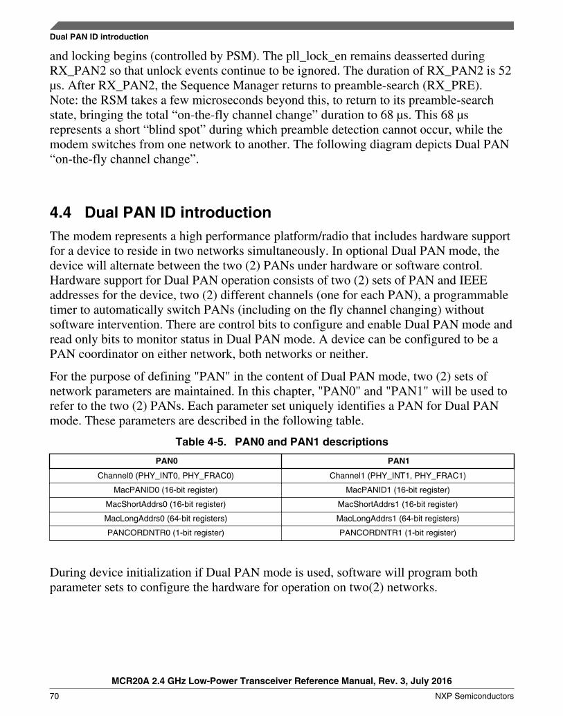
and locking begins (controlled by PSM). The pll_lock_en remains deasserted duringRX_PAN2 so that unlock events continue to be ignored. The duration of RX_PAN2 is 52µs. After RX_PAN2, the Sequence Manager returns to preamble-search (RX_PRE).Note: the RSM takes a few microseconds beyond this, to return to its preamble-searchstate, bringing the total “on-the-fly channel change” duration to 68 µs. This 68 µsrepresents a short “blind spot” during which preamble detection cannot occur, while themodem switches from one network to another. The following diagram depicts Dual PAN“on-the-fly channel change”.
4.4 Dual PAN ID introductionThe modem represents a high performance platform/radio that includes hardware supportfor a device to reside in two networks simultaneously. In optional Dual PAN mode, thedevice will alternate between the two (2) PANs under hardware or software control.Hardware support for Dual PAN operation consists of two (2) sets of PAN and IEEEaddresses for the device, two (2) different channels (one for each PAN), a programmabletimer to automatically switch PANs (including on the fly channel changing) withoutsoftware intervention. There are control bits to configure and enable Dual PAN mode andread only bits to monitor status in Dual PAN mode. A device can be configured to be aPAN coordinator on either network, both networks or neither.
For the purpose of defining "PAN" in the content of Dual PAN mode, two (2) sets ofnetwork parameters are maintained. In this chapter, "PAN0" and "PAN1" will be used torefer to the two (2) PANs. Each parameter set uniquely identifies a PAN for Dual PANmode. These parameters are described in the following table.
Table 4-5. PAN0 and PAN1 descriptions
PAN0 PAN1
Channel0 (PHY_INT0, PHY_FRAC0) Channel1 (PHY_INT1, PHY_FRAC1)
MacPANID0 (16-bit register) MacPANID1 (16-bit register)
MacShortAddrs0 (16-bit register) MacShortAddrs1 (16-bit register)
MacLongAddrs0 (64-bit registers) MacLongAddrs1 (64-bit registers)
PANCORDNTR0 (1-bit register) PANCORDNTR1 (1-bit register)
During device initialization if Dual PAN mode is used, software will program bothparameter sets to configure the hardware for operation on two(2) networks.
Dual PAN ID introduction
MCR20A 2.4 GHz Low-Power Transceiver Reference Manual, Rev. 3, July 2016
70 NXP Semiconductors
4.4.1 Manual and Automatic Modes
Two (2) modes are available for Dual PAN operation:
• Manual
• Automatic
4.4.1.1 Manual Dual PAN Mode
In manual Dual PAN mode software controls which PAN is selected for transmission andreception at all times. Software populates both PAN network parameter-set-registerslisted in Table 4-5 where software selects a PAN to begin transmission of reception. Asingle control bit ACTIVE_NETWORK selects the PAN. To select PAN0,ACTIVE_NETWORK should be set to 0; to select PAN1, ACTIVE_NETWORK shouldbe set to 1. Software then initiates an auto sequence by writing the appropriate value toXCVSEQ. At any point software can elect to switch to the alternate PAN. To switch,software aborts the sequence (if one is active) by writing XCVSEQ = IDLE. Softwarethen toggles ACTIVE_NETWORK and restarts a new sequence with XCVSEQ.Software is responsible for aborting and initiating sequences. Hardware is responsible forwarming up the transceiver on the selected channel (CHANNEL0 or CHANNEL1) andperforming address-filtering on the selected network's address parameters.(PANCORDNTR, MacPanID, Short Address and/or IEEE address).Software overhead issignificantly reduced in this mode because there is no need to re-program all of the PAN-select registers every time the PAN is toggled in Dual PAN mode where only a single bit(ACTIVE_NETWORK) needs to be written. For manual Dual PAN operation,DUAL_PAN_AUTO should be set to 0.
The diagram shown in the next figure depicts Dual PAN operation in manual mode. Inthis example, software populates both PAN parameter sets during initialization. Also,software elects to initiate packet reception on PAN1, so ACTIVE_NETWORK is set to 1.Software initiates the Sequence R by writing to XCVSEQ. Hardware warms up thereceiver on CHANNEL1 and enters preamble-search. In this example no packet isreceived but a data request from higher level software requires a switch to PAN0.Software responds by aborting the reception by writing Sequence 1 to XCVSEQ.Software then sets ACTIVE_NETWORK to 0 to select PAN0. In the example, softwareinitiates a Sequence TR. The hardware warms up the receiver for CCA on CHANNEL0,performs CCA (channel is idle), warms down the receiver and warms up the transmitteron CHANNEL0. Then, transmits the requested packet, warms down the transmitter andwarms up the receiver again (as per the auto sequence) on CHANNEL0 in order toreceive the acknowledge packet. The acknowledge packet is received and the auto
Chapter 4 Modem: Modes of Operation
MCR20A 2.4 GHz Low-Power Transceiver Reference Manual, Rev. 3, July 2016
NXP Semiconductors 71
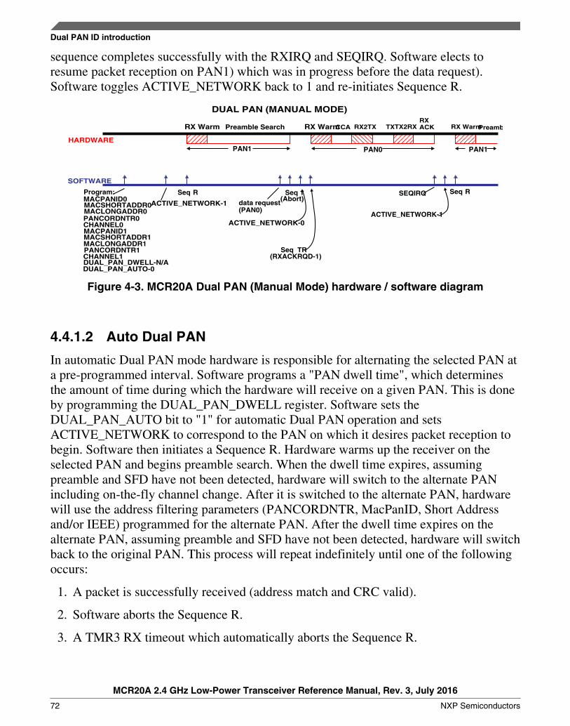
sequence completes successfully with the RXIRQ and SEQIRQ. Software elects toresume packet reception on PAN1) which was in progress before the data request).Software toggles ACTIVE_NETWORK back to 1 and re-initiates Sequence R.
DUAL PAN (MANUAL MODE)
RX Warm Preamble Search RX WarmCCA RX2TX TXTX2RXRXACK RX WarmPreamble
PAN1 PAN0 PAN1HARDWARE
SOFTWARE
Program:MACPANID0MACSHORTADDR0MACLONGADDR0PANCORDNTR0CHANNEL0MACPANID1MACSHORTADDR1MACLONGADDR1PANCORDNTR1CHANNEL1DUAL_PAN_DWELL-N/ADUAL_PAN_AUTO-0
Seq R
ACTIVE_NETWORK-1 data request(PAN0)
Seq 1(Abort)
ACTIVE_NETWORK-0
Seq TR(RXACKRQD-1)
Seq RSEQIRQ
ACTIVE_NETWORK-1
Figure 4-3. MCR20A Dual PAN (Manual Mode) hardware / software diagram
4.4.1.2 Auto Dual PAN
In automatic Dual PAN mode hardware is responsible for alternating the selected PAN ata pre-programmed interval. Software programs a "PAN dwell time", which determinesthe amount of time during which the hardware will receive on a given PAN. This is doneby programming the DUAL_PAN_DWELL register. Software sets theDUAL_PAN_AUTO bit to "1" for automatic Dual PAN operation and setsACTIVE_NETWORK to correspond to the PAN on which it desires packet reception tobegin. Software then initiates a Sequence R. Hardware warms up the receiver on theselected PAN and begins preamble search. When the dwell time expires, assumingpreamble and SFD have not been detected, hardware will switch to the alternate PANincluding on-the-fly channel change. After it is switched to the alternate PAN, hardwarewill use the address filtering parameters (PANCORDNTR, MacPanID, Short Addressand/or IEEE) programmed for the alternate PAN. After the dwell time expires on thealternate PAN, assuming preamble and SFD have not been detected, hardware will switchback to the original PAN. This process will repeat indefinitely until one of the followingoccurs:
1. A packet is successfully received (address match and CRC valid).
2. Software aborts the Sequence R.
3. A TMR3 RX timeout which automatically aborts the Sequence R.
Dual PAN ID introduction
MCR20A 2.4 GHz Low-Power Transceiver Reference Manual, Rev. 3, July 2016
72 NXP Semiconductors

4. A PLL unlock automatically aborts the Sequence R.
If the hardware PAN dwell timer expires during a packet reception (i.e., preamble andSFD have been detected during a Sequence R), the PAN-switch will be delayed until thepacket is completely received. If the packet was received successfully (address match andCRC valid), the receive sequence will terminate with RXIRQ and SEQIRQ (if an auto-Acknowledge was requested and enabled, the sequence will complete after theAcknowledge packet was transmitted, and TXIRQ will also be set, in addition to RXIRQand SEQIRQ); the PAN switch will occur at this point, after the Sequence has returned toIDLE. If the received packet fails FCS (CRC check), or, if the packet was not intendedfor the device (address mismatch), the hardware will toggle the PAN, and return topreamble-search on the new PAN.
If the hardware PAN dwell timer expires during a state other than RX preamble searchduring Sequence R (i.e., if expiration occurs during TX, CCA, ED, Sequence TR, or anywarm-up or transitional state), PAN-switch will be delayed until either:
1. Preamble Search state is reached during a Sequence R (not Sequence TR).
2. Sequence returns to IDLE.
At any point, software can elect to interrupt the automatic Dual PAN operation, byaborting the sequence with a XCVSEQ=IDLE, and the setting the DUAL_PAN_AUTObit to 0. In response, hardware will freeze the current state of the dwell timer, and capturethe currently-selected PAN, so that hardware-controlled PAN alternation can resumewhere it left off, later. Software can then tend to that tasks that caused the Dual PANinterruption. When software wants to resume Dual PAN operation, it then setsDUAL_PAN_AUTO=1, and re-initiates Sequence R. Hardware will resume the dwelltimer from the point it was frozen earlier, on the same PAN, and will warm-up thereceiver to receive on the PAN that was being monitored before the interruption.Hardware will dwell on that PAN until the timer expires, and then switch PAN's(assuming no preamble and SFD detected, subject to the conditions listed above).Software can always determine the selected PAN at any time, in any mode, by readingCURRENT_NETWORK bit. If DUAL_PAN_AUTO=0, then CURRENT_NETWORK =ACTIVE_NETWORK. If DUAL_PAN_AUTO=1, then CURRENT_NETWORK iscontrolled by hardware.
To initiate auto Dual PAN operation for the first time, or to reset the dwell timer to itsprogrammed value and allow software to select the initial PAN for auto Dual PANoperation, software should program the desired initial PAN to ACTIVE_NETWORK (0for PAN0, 1 for PAN1), and then program the desired dwell time into theDUAL_PAN_DWELL register. Hardware always responds to a write toDUAL_PAN_DWELL, by resetting the dwell timer to its programmed value, and
Chapter 4 Modem: Modes of Operation
MCR20A 2.4 GHz Low-Power Transceiver Reference Manual, Rev. 3, July 2016
NXP Semiconductors 73
selecting the initial PAN for auto Dual PAN operation, based on the state ofACTIVE_NETWORK. A write to DUAL_PAN_DWELL, always re-initializes theDWELL TIMER to the programmed value. If a write to DUAL_PAN_DWELL occursduring an auto sequence, the DWELL TIMER will begin counting down immediately. Ifa write to DUAL_PAN_DWELL occurs when there is no auto sequence underway, theDWELL TIMER will not begin counting until the next auto sequence begins; it willbegin counting at the start of the auto sequence warm-up. Under all circumstances,DUAL_PAN_AUTO must be asserted to allow the DWELL TIMER to count. IfDUAL_PAN_AUTO=0, the DWELL TIMER will freeze and hold its state, untilDUAL_PAN_AUTO=1. However, a write to DUAL_PAN_DWELL will still initializethe DWELL TIMER to its programmed value, regardless of the state ofDUAL_PAN_AUTO.
At any point during auto Dual PAN mode, software can ascertain the PAN currentlybeing serviced by hardware by reading the CURRENT_NETWORK bit. Software canalso determine the time remaining in the current dwell by reading theDUAL_PAN_REMAIN register.
In the auto Dual PAN mode, software retains responsibility for initiating and abortingsequences. There is no provision for hardware initiated sequences. TMR2 may be used toinitiate an auto sequence at a future time. TMR3 may be used as an RX hardware abortmechanism.
The following figure depicts Dual PAN operation in automatic mode. In this examplesoftware populates both PAN parameter sets during initialization. Software wants toinitiate packet reception in auto Dual PAN mode on PAN1, so ACTIVE_NETWORK isset to "1". For auto Dual PAN operation software programs the desired PAN-switchinginterval into DUAL_PAN_DWELL register, in this case 4 ms. Software initiates theSequence R by writing to XCVSEQ. The dwell timer begins counting as soon as thereceiver warm-up begins. Hardware warms up the receiver on CHANNEL1 where PANwas selected as the initial PAN shown in Figure 4-4 and begins preamble search. If apacket is received during this interval, hardware applies PAN1 address filtering. Nopreamble is detected at the point where the dwell timer expires so hardware executes aPAN-switch to PAN0 that includes an on-the-fly-change. On-the-fly changes requireapproximately 68 µs to execute and no preamble detection is possible during this "blindspot". After the PAN switch, hardware assumes preamble search on CHANNEL0 andapplies PAN0 address filtering if a packet is received. No preamble is detected at thepoint which the dwell timer expires, therefore hardware performs a PAN-switch back toPAN1 and so on and so forth.
Dual PAN ID introduction
MCR20A 2.4 GHz Low-Power Transceiver Reference Manual, Rev. 3, July 2016
74 NXP Semiconductors
DUAL PAN (AUTO MODE)
RX Warm Preamble Search
PAN1 PAN0 PAN1HARDWARE
SOFTWARE
on-the-fly channel change
MACPANID0MACSHORTADDR0MACLONGADDR0PANCORDNTR0CHANNEL0MACPANID1MACSHORTADDR1MACLONGADDR1PANCORDNTR1CHANNEL1DUAL_PAN_DWELL-4ms
DUAL_PAN_AUTO-1
Seq R
4ms 4ms 4ms
Program:
ACTIVE_NETWORK-1
Figure 4-4. MCR20A transceiver dual PAN auto mode diagram
4.4.1.3 Two-PAN-one-channel
A special case occurs if a device is operating in Dual PAN mode (either Auto or Manualmode), and both PAN's occupy the same channel; in other words,CHANNEL0=CHANNEL1. In this case, hardware will detect this condition, and applyboth sets of address-filtering parameters simultaneously. Hardware will provide DataIndication if the received packet matches either the PAN0 address parameter set{MacPanID0, MacShortAddrs0, MacLongAddrs0, PANCORDNTR0}, or the PAN1address parameter set {MacPanID1, MacShortAddrs1, MacLongAddrs1,PANCORDNTR1}. At Data Indication, two status bits can be queried by software toquickly determine on which PAN the packet was received, RECD_ON_PAN0 orRECD_ON_PAN1. In the "Two-PAN-one-channel" scenario, it is possible for a packet tosatisfy both sets of addressing parameters (PAN0 and PAN1). When this happens, bothRECD_ON_PAN0 and RECD_ON_PAN1 will be set. In the "Two-PAN-one-channel"scenario, the CURRENT_NETWORK bit should be ignored, because both networks aresimultaneously active.
If Dual PAN mode is not to be used, ACTIVE_NETWORK should be maintained at 0(default) to select the PAN0 parameters for transceiving. In single PAN operation, thePAN1 parameter registers need not be programmed, and can be used as scratchpad.(PLL_INT1 and PLL_FRAC1 should not be programmed, and should instead be left intheir default state, if Dual PAN mode is not in use).
Chapter 4 Modem: Modes of Operation
MCR20A 2.4 GHz Low-Power Transceiver Reference Manual, Rev. 3, July 2016
NXP Semiconductors 75
4.4.2 Source Address Matching
This section describes interaction between Dual PAN mode and the modem packetProcessors Source Address Matching function. The Source Address Matching Table istwo (2) entries deep and 16 bits wide. In Dual PAN mode, entries from both networkswill need to be stored in the table. It is highly undesirable to add a 17th bit to each tableentry merely to identify the network on which the packet containing the Source Addresswas received. In order to keep the Source Address table width at 16 bits, the table will besplit into two (2) sections:
• Lower section shall hold "PAN0" source address checksums
• Upper section shall hold "PAN1" source address checksums
In Dual PAN mode when software populates the table with a new Source AddressChecksum, it will deposit the new checksum in the appropriate section of the table basedupon whether the packet was received on PAN0 or PAN1. When the Packet Processorinterrogates the table for a matching checksum, it will only search the section of the tablecorresponding to the PAN on which the current packet is being received. The dividing-line between the PAN0 and PAN1 sections in the table shall be programmability with a4-bit register DUAL_PAN_SAM_LVL (SAM is an acronym for "Source AddressMatching"). The register identifies the first PAN1 entry in the table (indices below thislevel apply to PAN0). For single-PAN operation, software should set this register to "12"or above which dedicates the entire table to PAN0. The hardware shall reset-default thisregister to "12". Figure 4-5 shows the effect of setting the PAN dividing line to "8":
SOURCE ADDRESS TABLE
REGISTERDUAL_PAN_SAM_LVL[3:0]
7 6 5 4 3 2 1
0
0
1
2
3
4
5
6
7
8
9
10
11
16 bits
PAN0
PAN1
set to '8'in this example
Figure 4-5. Source Address table set to "8"
Dual PAN ID introduction
MCR20A 2.4 GHz Low-Power Transceiver Reference Manual, Rev. 3, July 2016
76 NXP Semiconductors
4.4.3 Programming interface
This section describes registers associated with the Dual PAN ID. All writable registersread back what was previously written by software. Register addresses within theMCR20A tranceiver's memory map and bit assignments are shown below.
Table 4-6. MCR20A memory map and bit assignments
Register NameAccessMode
Width Description
DUAL_PAN_AUTO rw 1 Activates automatic Dual PAN operating mode. In this mode, PAN-switching is controlled by hardware at a pre-programmed rate, determinedby DUAL_PAN_DWELL.
1: Auto Dual PAN Mode
0: Manual Dual PAN mode (or Single PAN mode). Default.
Whenever DUAL_PAN_AUTO=0,CURRENT_NETWORK=ACTIVE_NETWORK at all times. In other words,software directly controls which PAN is selected.
Whenever DUAL_PAN_AUTO=1, CURRENT_NETWORK is controlled byHW
ACTIVE_NETWORK rw 1 Selects the PAN on which to transceiver, by activating a PAN parameterset (PAN0 or PAN1). In Manual Dual PAN mode (or Single PAN mode),this bit selects the active PAN parameter set (channel and addressingparameters) that governs all auto sequences. In Auto Dual PAN mode, thisbit selects the PAN on which to begin transceiving, latched at the point atwhich DUAL_PAN_DWELL register is written.
0: Select PAN0 (Default)
CURRENT_NETWORK r 1 This read only bit indicates which PAN is currently selected by hardware inautomatic Dual PAN mode.
1: PAN1 is selected
0: PAN0 is selected
DUAL_PAN_DWELL rw 8 Channel Frequency Dwell Time. In Auto Dual PAN mode, hardware willtoggle the PAN, after dwelling on the current PAN for the intervaldescribed below (assuming Preamble/SFD not detected). A write toDUAL_PAN_DWELL, always re-initializes the DWELL TIMER to theprogrammed value. If a write to DUAL_PAN_DWELL occurs during anauto sequence, the DWELL TIMER will begin counting down immediately.If a write to DUAL_PAN_DWELL occurs when there is no auto sequenceunderway, the DWELL TIMER will not begin counting until the next autosequence begins; it will begin counting at the start of the sequence warm-up.
PRESCALER TIMEBASE RANGEbits [1:0] (min) - (max)(2 bits) (6 bits)------- ---------- -------------00 0.5 ms 0.5 - 32 ms01 2.5 ms 2.5 - 160 ms10 10 ms 10 - 640 ms11 50 ms 50 - 3.2 seconds
Table continues on the next page...
Chapter 4 Modem: Modes of Operation
MCR20A 2.4 GHz Low-Power Transceiver Reference Manual, Rev. 3, July 2016
NXP Semiconductors 77

Table 4-6. MCR20A memory map and bit assignments (continued)
Register NameAccessMode
Width Description
A write to DUAL_PAN_DWELL also causes the value ofACTIVE_NETWORK to get latched into the hardware. This latched valuewill be the starting point for the automatic dual-pan mode (i.e., start onPAN0 or on PAN1). The starting value takes effect immediately (ifsequence is underway and DUAL_PAN_AUTO=1), or is otherwise delayeduntil sequence starts and DUAL_PAN_AUTO=1.
DUAL_PAN_REMAIN r 6 This read only register indicates time remaining before next PAN switch inauto Dual PAN mode. The units for this register depend on thePRESCALAR setting in the DUAL_PAN_DWELL register according to thefollowing table
DUAL_PAN_DWELL DUAL_PAN_REMAINPRESCALAR UNITS00 0.5 ms01 2.5 ms10 10 ms11 50 ms
The readback value indicates that between N-1 and N timebase unitsremain until the next PAN switch. For example, a DUAL_PAN_REMAINreadback value of 3, with a DUAL_PAN_DWELL PRESCALER setting of 2(10ms), indicates that between 20ms (2*10ms) and 30ms (3*10ms),remain until the next automatic PAN switch.
RECD_ON_PAN0 r 1 Indicates the packet which was just received was received on PAN0
RECD_ON_PAN1 r 1 Indicates the packet which was just received was received on PAN1
DUAL_PAN_SAM_LVL rw 4 For the Source Address Matching Table, sets the dividing line betweenPAN0 and PAN1 sections of the table. Table indices at or above this levelbelong to PAN1. Table entries below this level belong to PAN0. Default =12 (entire table is PAN0).
CHANNEL0 rw 4 Channel selector for PAN0
MACPANID0 rw 16 MAC PAN ID for PAN0
MACSHORTADDRS0 rw 16 MAC Short Address fro PAN0
MACLONGADDRS0 rw 64 MAC Long Address fro PAN0
PANCORDNTR0 rw 1 1: Device is a PAN Coordinator on PAN0
0: Device is not a PAN Coordinator on PAN0
CHANNEL1 rw 4 Channel selector for PAN1
MACPANID1 rw 16 MAC PAN ID for PAN1
MACSHORTADDRS1 rw 16 MAC Short Address fro PAN1
MACLONGADDRS1 rw 64 MAC Long Address fro PAN1
PANCORDNTR1 rw 1 1: Device is a PAN Coordinator on PAN1
0: Device is not a PAN Coordinator on PAN1
Dual PAN ID introduction
MCR20A 2.4 GHz Low-Power Transceiver Reference Manual, Rev. 3, July 2016
78 NXP Semiconductors
4.5 Active Promiscuous ModeThis section describes the Active Promiscuous mode for the MCR20A transceiver highperformance 2.4 GHz IEEE 802.15.4 radio.
4.5.1 Functional Description
The 802.15.4 Wireless Medium Access Control (MAC) and Physical Layer (PHY)specifications for Low-Rate Wireless Personal Area Networks (WPAN's) prescribes thefollowing behavior for Promiscuous mode operation.
In promiscuous mode, the MAC sublayer passes all frames received after the first filterdirectly to the upper layers without applying and more filtering or processing.
Where the first level is described as:
For the first level of filtering, the MAC sublayer shall disregard all received frames thatdo not contain a correct value in their FCS field in the MFR (see section 7.2.1.9 in thestandard specification).
Promiscuous mode allows a device to receive and process all 802.15.4 frames that passFCS check (CRC), regardless of whether or not they are addressed to the device. Thisallows a device to receive and process all valid traffic on the network. In Promiscuousmode, the modem packet processor will provide Data Indication on all packets. Thiscapability allows a simple network sniffer to be constructed, which can displaycomprehensive packet data for all packets transmitted on a network within receivingrange of the device.
Because a device operating in Promiscuous mode is designed to do so discretely,automatic acknowledgement of all received packets is inhibited regardless of the state ofthe ACK request in the Frame Control Field of the received packet. Otherwise, thesniffing device would be acknowledging received frames for which it was not theaddress.
In Active Promiscuous mode the packet processor will process packets according to thesame rules that it applies to Promiscuous mode, except that it will automatically transmitan acknowledgement packet for frames that were addressed to the device. In other words,in Active Promiscuous mode if the received frame meets all the address and packetfiltering requirements that would have been applied in non-promiscuous mode anacknowledgment packet will be transmitted; a Data Indication will still be provided forall packets (those that pass FCS check).
Chapter 4 Modem: Modes of Operation
MCR20A 2.4 GHz Low-Power Transceiver Reference Manual, Rev. 3, July 2016
NXP Semiconductors 79
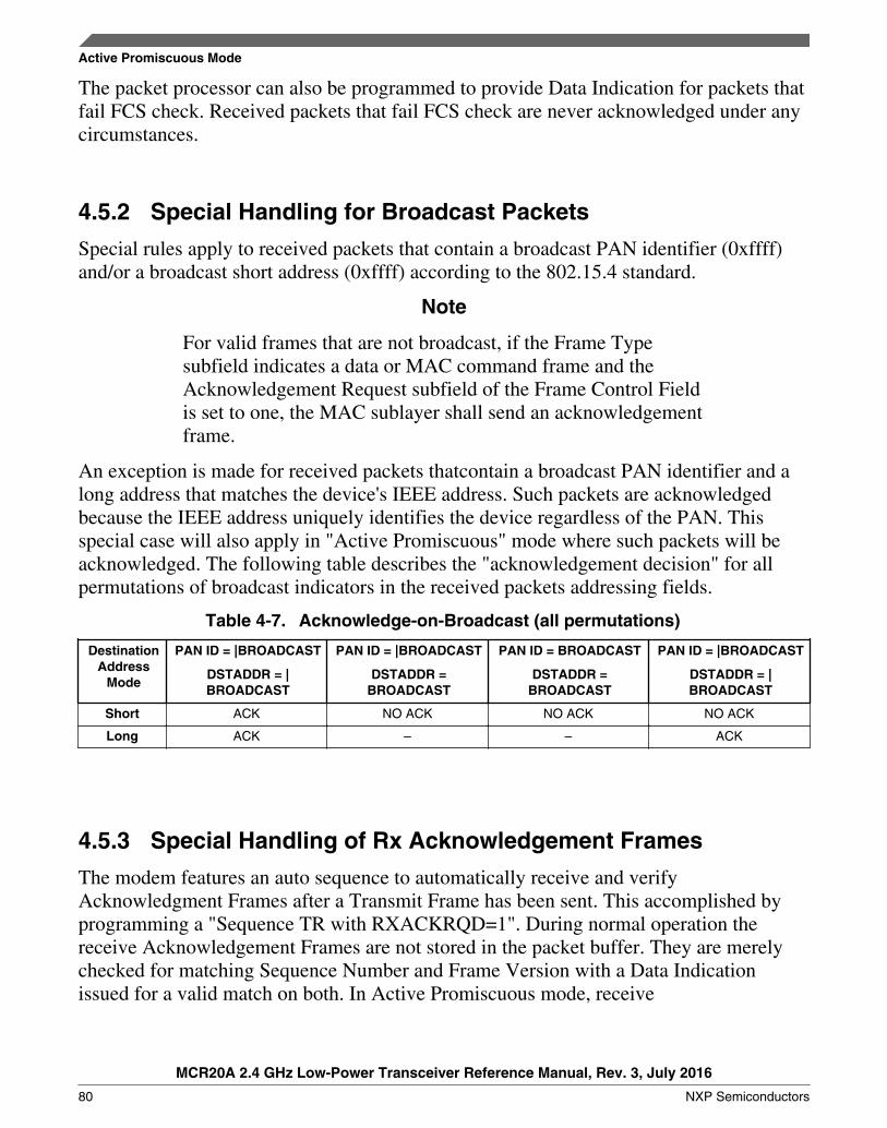
The packet processor can also be programmed to provide Data Indication for packets thatfail FCS check. Received packets that fail FCS check are never acknowledged under anycircumstances.
4.5.2 Special Handling for Broadcast Packets
Special rules apply to received packets that contain a broadcast PAN identifier (0xffff)and/or a broadcast short address (0xffff) according to the 802.15.4 standard.
Note
For valid frames that are not broadcast, if the Frame Typesubfield indicates a data or MAC command frame and theAcknowledgement Request subfield of the Frame Control Fieldis set to one, the MAC sublayer shall send an acknowledgementframe.
An exception is made for received packets thatcontain a broadcast PAN identifier and along address that matches the device's IEEE address. Such packets are acknowledgedbecause the IEEE address uniquely identifies the device regardless of the PAN. Thisspecial case will also apply in "Active Promiscuous" mode where such packets will beacknowledged. The following table describes the "acknowledgement decision" for allpermutations of broadcast indicators in the received packets addressing fields.
Table 4-7. Acknowledge-on-Broadcast (all permutations)
DestinationAddress
Mode
PAN ID = |BROADCAST
DSTADDR = |BROADCAST
PAN ID = |BROADCAST
DSTADDR =BROADCAST
PAN ID = BROADCAST
DSTADDR =BROADCAST
PAN ID = |BROADCAST
DSTADDR = |BROADCAST
Short ACK NO ACK NO ACK NO ACK
Long ACK – – ACK
4.5.3 Special Handling of Rx Acknowledgement Frames
The modem features an auto sequence to automatically receive and verifyAcknowledgment Frames after a Transmit Frame has been sent. This accomplished byprogramming a "Sequence TR with RXACKRQD=1". During normal operation thereceive Acknowledgement Frames are not stored in the packet buffer. They are merelychecked for matching Sequence Number and Frame Version with a Data Indicationissued for a valid match on both. In Active Promiscuous mode, receive
Active Promiscuous Mode
MCR20A 2.4 GHz Low-Power Transceiver Reference Manual, Rev. 3, July 2016
80 NXP Semiconductors

Acknowledgement Frames will be stored into the Packet Buffer just like any otherreceive frame. This saves software from having to re-construct the contents of theAcknowledgement packet from the contents of the packet that was originally transmitted.
4.5.4 Programming Interface
This section describes registers associated with Active Promiscuous Mode. The definitionand functionality of the PROMISCUOUS bit, which will be maintained for the modem isidentical to existing FSL 802.15.4 transceivers. The ACTIVE_PROMISCUOUS bit isnew for the modem as shown in the following table.
Table 4-8. ACTIVE_PROMISCUOUS register
Register Name Access Mode Width Description
ACTIVE_PROMISCUOUS rw 1 1: Provide Data Indication on all received packets under thesame rules that apply in PROMISCUOUS mode, howeveracknowledge those packets under rules that apply in non-PROMISCUOUS mode
0: normal operation (Default)
Clock System
4.6.1 32 MHz Crystal Oscillator
The 32 MHz crystal oscillator (XTAL32m) is composed of the following features:
• Amplifier — it associates with an external crystal and tuning capacitors creating themain oscillator loop.
• Hysteresis comparator — it creates a logic-level signal from the sine wave developedacross the crystal terminals.
• Clock gate timer — it waits for a delay before passing the clock signal.• Clock divider that contains a divider by two and divide by eight circuitry.
The XTAL32m frequency is 32 MHz. It can be trimmed with some internal capacitancesconnected on both pads. The XTAL32m is supplied by the VBAT. An external clockgenerator can be connected to XTAL32Mout. In this case, the clock is directly connectedto the output in bypass mode. A 1.8 V square clock can be connected as required.
The crystal oscillator block can work in 2 modes:
4.6
Chapter 4 Modem: Modes of Operation
MCR20A 2.4 GHz Low-Power Transceiver Reference Manual, Rev. 3, July 2016
NXP Semiconductors 81
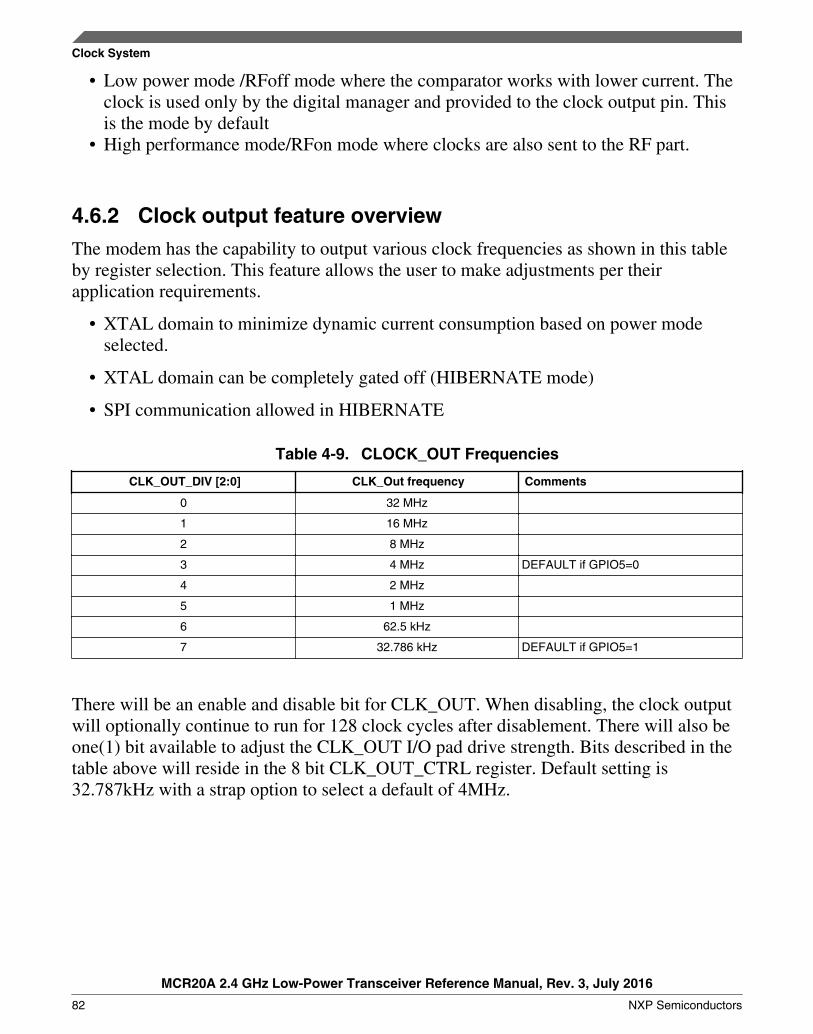
• Low power mode /RFoff mode where the comparator works with lower current. Theclock is used only by the digital manager and provided to the clock output pin. Thisis the mode by default
• High performance mode/RFon mode where clocks are also sent to the RF part.
4.6.2 Clock output feature overview
The modem has the capability to output various clock frequencies as shown in this tableby register selection. This feature allows the user to make adjustments per theirapplication requirements.
• XTAL domain to minimize dynamic current consumption based on power modeselected.
• XTAL domain can be completely gated off (HIBERNATE mode)
• SPI communication allowed in HIBERNATE
Table 4-9. CLOCK_OUT Frequencies
CLK_OUT_DIV [2:0] CLK_Out frequency Comments
0 32 MHz
1 16 MHz
2 8 MHz
3 4 MHz DEFAULT if GPIO5=0
4 2 MHz
5 1 MHz
6 62.5 kHz
7 32.786 kHz DEFAULT if GPIO5=1
There will be an enable and disable bit for CLK_OUT. When disabling, the clock outputwill optionally continue to run for 128 clock cycles after disablement. There will also beone(1) bit available to adjust the CLK_OUT I/O pad drive strength. Bits described in thetable above will reside in the 8 bit CLK_OUT_CTRL register. Default setting is32.787kHz with a strap option to select a default of 4MHz.
Clock System
MCR20A 2.4 GHz Low-Power Transceiver Reference Manual, Rev. 3, July 2016
82 NXP Semiconductors
Chapter 5Modem: Advanced Security Module
5.1 Advanced Security Module
5.2 IntroductionThe ASM engine encrypts using the Advanced Encryption Standard (AES). It canperform Counter (CTR), Cipher Block Chaining (CBC), and plain AES mode encryption.The combination of CTR and CBC modes of encryption is known as CCM modeencryption. CCM is short for Counter with CBC-MAC. CCM is a generic authenticateand encrypt block cipher mode. CCM is defined for use only with 128 bit block ciphers,such as AES.
5.2.1 Features
The ASM has the following features:
• CTR encryption.
• CBC encryption.
• AES encryption.
• Encrypts 128 bits as a unit.
MCR20A 2.4 GHz Low-Power Transceiver Reference Manual, Rev. 3, July 2016
NXP Semiconductors 83
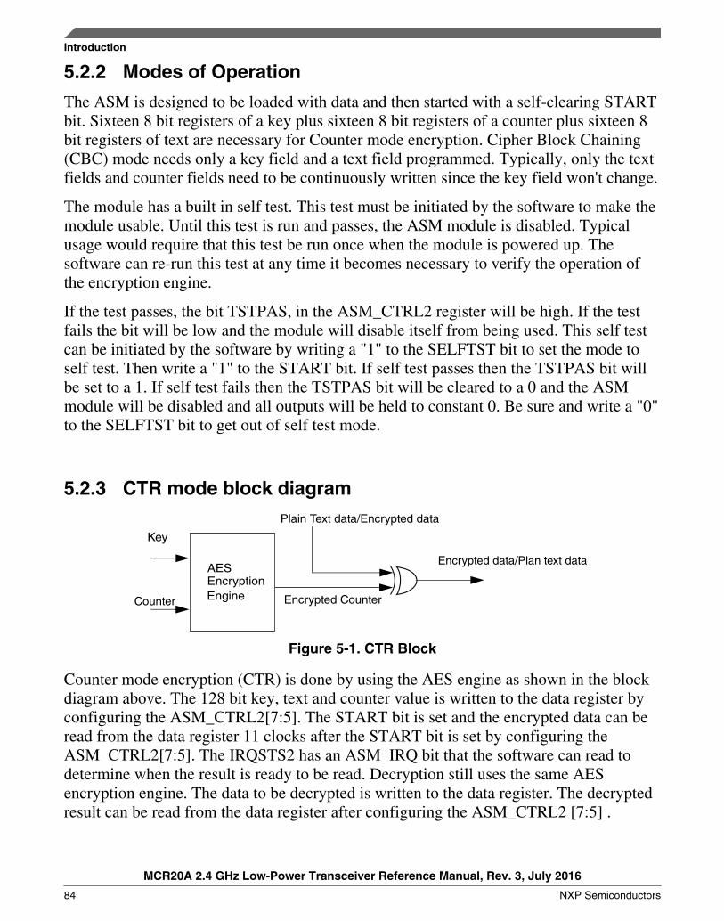
5.2.2 Modes of Operation
The ASM is designed to be loaded with data and then started with a self-clearing STARTbit. Sixteen 8 bit registers of a key plus sixteen 8 bit registers of a counter plus sixteen 8bit registers of text are necessary for Counter mode encryption. Cipher Block Chaining(CBC) mode needs only a key field and a text field programmed. Typically, only the textfields and counter fields need to be continuously written since the key field won't change.
The module has a built in self test. This test must be initiated by the software to make themodule usable. Until this test is run and passes, the ASM module is disabled. Typicalusage would require that this test be run once when the module is powered up. Thesoftware can re-run this test at any time it becomes necessary to verify the operation ofthe encryption engine.
If the test passes, the bit TSTPAS, in the ASM_CTRL2 register will be high. If the testfails the bit will be low and the module will disable itself from being used. This self testcan be initiated by the software by writing a "1" to the SELFTST bit to set the mode toself test. Then write a "1" to the START bit. If self test passes then the TSTPAS bit willbe set to a 1. If self test fails then the TSTPAS bit will be cleared to a 0 and the ASMmodule will be disabled and all outputs will be held to constant 0. Be sure and write a "0"to the SELFTST bit to get out of self test mode.
5.2.3 CTR mode block diagram
Key
Counter
AESEncryptionEngine
Plain Text data/Encrypted data
Encrypted data/Plan text data
Encrypted Counter
Figure 5-1. CTR Block
Counter mode encryption (CTR) is done by using the AES engine as shown in the blockdiagram above. The 128 bit key, text and counter value is written to the data register byconfiguring the ASM_CTRL2[7:5]. The START bit is set and the encrypted data can beread from the data register 11 clocks after the START bit is set by configuring theASM_CTRL2[7:5]. The IRQSTS2 has an ASM_IRQ bit that the software can read todetermine when the result is ready to be read. Decryption still uses the same AESencryption engine. The data to be decrypted is written to the data register. The decryptedresult can be read from the data register after configuring the ASM_CTRL2 [7:5] .
Introduction
MCR20A 2.4 GHz Low-Power Transceiver Reference Manual, Rev. 3, July 2016
84 NXP Semiconductors

5.2.4 CBC mode block diagramKey
AESEncryptionEnginePlain text data
Cipher block chaining message authentication code
CBC MAC value
Figure 5-2. CBC Block
The CBC-MAC generation is done by using the AES engine as shown in the blockdiagram above. The 128 bit key and data is written to data register by configuring theASM_CTRL2[7:5] . The start bit is set and the MAC value can be read from the dataregister 11 clocks after the start bit is set after configuring the ASM_CTRL2[7:5]. TheASM_IRQ bit can be read from the IRQSTS2 to determine when the result is complete.
5.2.5 CCM mode
CCM mode is the combination of using CTR mode for protecting the privacy of data, andusing CBC mode to generate a MAC to protect the data from unauthorized modifications.In this mode both CTR and CBC bits in the ASM_CTRL1 are set and the START bit isset. The ASM first performs a CTR encryption followed by a CBC conversion. Theresults of CTR and CBC conversion are stored in separate registers which can be read byconfiguring the DATA_REG_TYPE_SELECT bits in ASM_CTRL2.
5.2.6 AES mode
AES mode is the most simple method of encryption in which there is no feedback ofresult to input in any form. The user simply writes the inputs required to the data registersand reads the result from the result register. For this mode, the user must clear both theCTR and CBC bits in the ASM_CTRL1 and set the AES bit followed by START bit tobegin the conversion process. After 11 clock cycles the result is available in the resultregister, which can be read by configuring the DATA_REG_TYPE_SELECT bits fromthe ASM_CTRL2.
Chapter 5 Modem: Advanced Security Module
MCR20A 2.4 GHz Low-Power Transceiver Reference Manual, Rev. 3, July 2016
NXP Semiconductors 85
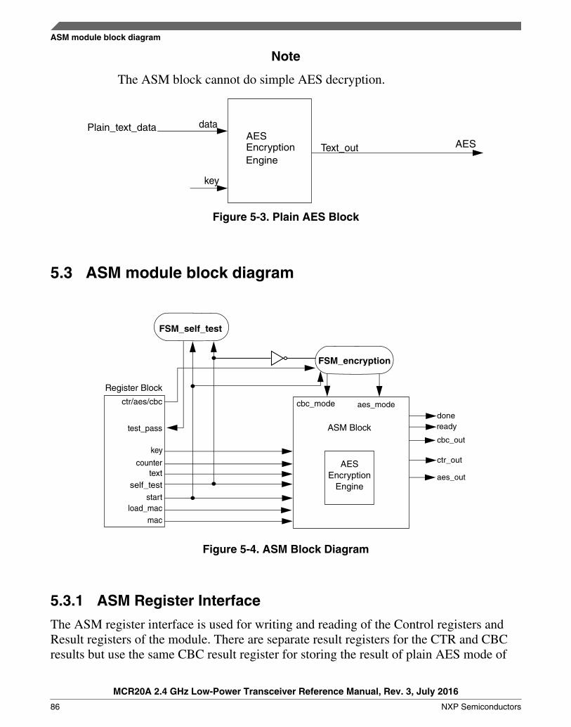
Note
The ASM block cannot do simple AES decryption.
dataAESEncryptionEngine
Text_out AES
Plain_text_data
key
Figure 5-3. Plain AES Block
5.3 ASM module block diagram
FSM_self_test
FSM_encryption
cbc_mode aes_modedoneready
cbc_out
ctr_out
aes_out
ctr/aes/cbc
test_pass
textself_test
startload_mac
mac
AESEncryption
Engine
key
counter
ASM Block
Register Block
Figure 5-4. ASM Block Diagram
5.3.1 ASM Register Interface
The ASM register interface is used for writing and reading of the Control registers andResult registers of the module. There are separate result registers for the CTR and CBCresults but use the same CBC result register for storing the result of plain AES mode of
ASM module block diagram
MCR20A 2.4 GHz Low-Power Transceiver Reference Manual, Rev. 3, July 2016
86 NXP Semiconductors
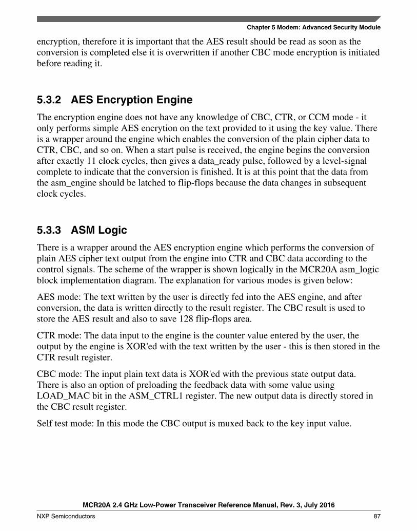
encryption, therefore it is important that the AES result should be read as soon as theconversion is completed else it is overwritten if another CBC mode encryption is initiatedbefore reading it.
5.3.2 AES Encryption Engine
The encryption engine does not have any knowledge of CBC, CTR, or CCM mode - itonly performs simple AES encrytion on the text provided to it using the key value. Thereis a wrapper around the engine which enables the conversion of the plain cipher data toCTR, CBC, and so on. When a start pulse is received, the engine begins the conversionafter exactly 11 clock cycles, then gives a data_ready pulse, followed by a level-signalcomplete to indicate that the conversion is finished. It is at this point that the data fromthe asm_engine should be latched to flip-flops because the data changes in subsequentclock cycles.
5.3.3 ASM Logic
There is a wrapper around the AES encryption engine which performs the conversion ofplain AES cipher text output from the engine into CTR and CBC data according to thecontrol signals. The scheme of the wrapper is shown logically in the MCR20A asm_logicblock implementation diagram. The explanation for various modes is given below:
AES mode: The text written by the user is directly fed into the AES engine, and afterconversion, the data is written directly to the result register. The CBC result is used tostore the AES result and also to save 128 flip-flops area.
CTR mode: The data input to the engine is the counter value entered by the user, theoutput by the engine is XOR'ed with the text written by the user - this is then stored in theCTR result register.
CBC mode: The input plain text data is XOR'ed with the previous state output data.There is also an option of preloading the feedback data with some value usingLOAD_MAC bit in the ASM_CTRL1 register. The new output data is directly stored inthe CBC result register.
Self test mode: In this mode the CBC output is muxed back to the key input value.
Chapter 5 Modem: Advanced Security Module
MCR20A 2.4 GHz Low-Power Transceiver Reference Manual, Rev. 3, July 2016
NXP Semiconductors 87
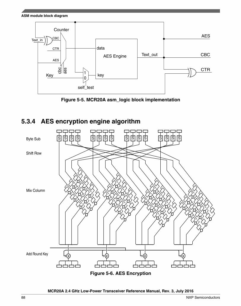
Text_in
Counter
CBC
CTR
AES
Key
cbc
aes
data
AES Engine
key
self_test
Text_out CBC
CTR
AES
10
Figure 5-5. MCR20A asm_logic block implementation
5.3.4 AES encryption engine algorithm
Byte Sub
Shift Row
Mix Column
Add Round Key
S S S S S S S S S S S S S S S S
Figure 5-6. AES Encryption
ASM module block diagram
MCR20A 2.4 GHz Low-Power Transceiver Reference Manual, Rev. 3, July 2016
88 NXP Semiconductors
The above diagram documents the encryption process for a single round. Each 128 bitdata block is iterated though this structure 10 times. Each time though the round key isupdated with a new value.
5.4 Counter mode encryption11 clocks to complete
• Program ASM_CTRL2[7:5] to 3'b000. Write the key value in the data registers.
• Set the bit "CTR" in ASM_CTRL1. The "CTR" bit is static.
• Program ASM_CTRL2 [7:5] to 3'b001. Write the text value in data registers.
• Program ASM_CTRL2 [7:5] to 3'b010. Write the counter value in data registers.
• Set the START bit in ASM_CTRL1. The START bit is a self clearing bit.
• Poll for the ASM_IRQ bit to be set to a "1", or wait for the ASM_IRQ interruptsignal.
• Program ASM_CTRL2 [7:5] to 3'b011. Read the encrypted text from data registers.
• Repeat steps 3-7 for each 128 bits block.
5.5 AES mode encryption11 clocks to complete
• Program ASM_CTRL2[7:5] to 3'b000. Write the key value in the data registers.
• Clear both CTR and CBC bit in ASM_CTRL1 and set AES bit.
• Program ASM_CTRL2 [7:5] to 3'b001. Write the text value in data registers.
• Program ASM_CTRL2 [7:5] to 3'b010. Write the counter value in data registers.
• Set the START bit in ASM_CTRL1. The START bit is a self clearing bit.
• Poll for the ASM_IRQ bit to be set to a "1", or wait for the ASM_IRQ interruptsignal.
• Program ASM_CTRL2[7:5] to 3'b110. Read the encrypted text from data registers.
• Repeat steps 3-7 for each 128 bits block.
Chapter 5 Modem: Advanced Security Module
MCR20A 2.4 GHz Low-Power Transceiver Reference Manual, Rev. 3, July 2016
NXP Semiconductors 89
5.6 Message Authentication Code generation (MAC)11 clocks to complete
• Program ASM_CTRL2 [7:5] to 3'b000. Program the key value in registers
• Set the bit CBC in ASM_CTRL1.
• Program ASM_CTRL2 [7:5] to 3'b001.Program the text value in registers
• Set the START bit in ASM_CTRL1. The START bit is a self clearing bit.
• Poll for the ASM_IRQ bit to be set to a "1", or wait for the ASM_IRQ interruptsignal.
• Repeat steps 3-6 for each 128 bits block.
• When all blocks have been processed, program ASM_CTRL2 [7:5] to 3'b100 andread the final MAC (authentication code) from data registers.
• The MAC accumulator should be cleared to prepare for the next payload. Writing a 1to the clear bit will set the MAC accumulator back to all 0. The clear bit is selfclearing. If for some reason the software needs to continue a MAC calculation from apreviously saved value, the MAC accumulator can be pre-loaded with a initial value.Program ASM_CTRL2 [7:5] to 3'b101 now the value you wish to load into theaccumulator is written to data registers and then a 1 is written to the LOAD_MACbit. The LOAD_MAC bit is self clearing.
• After self-test the CBC result register will have some initial value, so if the userwants to start a fresh transaction then the CBC result register has to be cleared bysetting the CLEAR bit in the ASM_CTRL1 register. It will clear all the contents ofthe CTR and CBC result register.
Message Authentication Code generation (MAC)
MCR20A 2.4 GHz Low-Power Transceiver Reference Manual, Rev. 3, July 2016
90 NXP Semiconductors
Chapter 6Modem: Interrupts
6.1 IntroductionInterrupts provide a way for the radio to inform the host microcontroller (MCU) ofonboard events without requiring the MCU to query for status. The following sectionsdescribe the interrupt features and sources of the modem.
• 13 interrupt sources (interrupt status bits)• Each interrupt source individually maskable• Each interrupt source is individually write-1-to-clear.• Interrupts remain asserted until cleared.
6.2 Modem Interrupt SourcesThe radio has a single, active low, interrupt pin (IRQ_B) provided to the MCU. Theinterrupt pin is configured as actively-driven by the radio. Internally, the radio has 13interrupt sources as shown in this table:
Table 6-1. Modem Interrupt Sources
Item Interrupt Sources
Status Bit
Mask Bit Description Interrupt Clear
Mechanism
1 PLL_UNLOCK_IRQ PLL_UNLOCK_MSK PLL Unlock Interrupt. A '1' indicates anunlock event has occurred in the PLL.
write-1-to-clear
2 FILTERFAIL_IRQ FILTERFAIL_MSK RX Packet has Failed Filtering. A '1'indicates the most-recently receivedpacket has been rejected due toelements within the packet.
In Dual PAN mode, FILTERFAIL_IRQapplies to either or both networks, asfollows:
write-1-to-clear
Table continues on the next page...
MCR20A 2.4 GHz Low-Power Transceiver Reference Manual, Rev. 3, July 2016
NXP Semiconductors 91
Table 6-1. Modem Interrupt Sources (continued)
Item Interrupt Sources
Status Bit
Mask Bit Description Interrupt Clear
Mechanism
A: If PAN0 and PAN1 occupy differentchannels and CURRENT_NETWORK=0,FILTERFAIL_IRQ applies to PAN0.
B: If PAN0 and PAN1 occupy differentchannels and CURRENT_NETWORK=1,FILTERFAIL_IRQ applies to PAN1.
C: If PAN0 and PAN1 occupy the samechannel, FILTERFAIL_IRQ is the logical'AND' of the individual PANs' Filter Failstatus.
3 RXWTRMRKIRQ RX_WMRK_MSK RX Byte Count Watermark Interrupt. A '1'indicates the number of bytes specifiedin the RX_WTR_MARK register hasbeen reached.
write-1-to-clear
4 CCAIRQ CCAMSK CCA Interrupt. A '1' indicates thecompletion of a CCA operation.
write-1-to-clear
5 RXIRQ RXMSK RX Interrupt. A '1' indicates thecompletion of a receive operation.
write-1-to-clear
6 TXIRQ TXMSK TX Interrupt. A '1' indicates thecompletion of a transmit operation.
write-1-to-clear
7 SEQIRQ SEQMSK Sequence Complete Interrupt. A '1'indicates the completion of anautosequence. This interrupt will assertwhenever the Sequence Managertransitions from non-idle to idle state, forany reason.
write-1-to-clear
8 PB_ERR_IRQ PB_ERR_MSK Packet Buffer Error Interrupt.
1: Packet Buffer Underrun Error hasoccurred since the last time this bit wascleared by software
0: Packet Buffer Underrun Error has notoccurred since the last time this bit wascleared by software.
Note: PB_ERR_IRQ will occur onlywhen the SPI Packet Buffer access isBURST mode (not BYTE mode)
write-1-to-clear
9 WAKE_IRQ WAKE_MSK Wake Interrupt. Indicates either a Wake-from-POR or Wake-from-HIBERNATEevent has occurred.
The WAKE_FROM_HIB/TMRSTATUSbit indicates which type of wake eventoccurred, as long as WAKE_IRQ=1.
write-1-to-clear
10 TMR1IRQ TMR1MSK TMR1 Interrupt. Indicates T1CMPcomparator value matched event timercounter.
write-1-to-clear
Table continues on the next page...
Modem Interrupt Sources
MCR20A 2.4 GHz Low-Power Transceiver Reference Manual, Rev. 3, July 2016
92 NXP Semiconductors
Table 6-1. Modem Interrupt Sources (continued)
Item Interrupt Sources
Status Bit
Mask Bit Description Interrupt Clear
Mechanism
11 TMR2IRQ TMR2MSK TMR2 Interrupt. Indicates comparatorvalue matched event timer counter. Thisflag is shared between the T2CMP (24-bit) and T2PRIMECMP (16-bit) compareregisters.
write-1-to-clear
12 TMR3IRQ TMR3MSK TMR3 Interrupt. Indicates T3CMPcomparator value matched event timercounter.
write-1-to-clear
13 TMR4IRQ TMR4MSK TMR4 Interrupt. Indicates T4CMPcomparator value matched event timercounter.
write-1-to-clear
Each interrupt can be controlled by an interrupt mask. All interrupts are OR- combinedwith the external pin IRQ_B. The IRQ is issued when IRQ_B is set to 0.
Any or all of the interrupt sources, can be enabled to cause an assertion on IRQ_B. Eachinterrupt source has its own interrupt status bit in modems Direct Register space. Eachinterrupt source is individually maskable (each has its own MASK bit) so that eachinterrupt source can be individual enabled to trigger an assertion on IRQ_B.
There is also a global interrupt mask, TRCV_MSK (PHY_CTRL4 register), which canenable/disable all IRQ_B assertions by programming a single masking bit. All 13interrupt status bits use a write-1-to-clear protocol. Interrupt status bits are not affected byreads. The IRQ_B pin is a level-sensitive interrupt indicator to the MCU; on an interrupt,IRQ_B will remain asserted until all active interrupt sources are cleared or masked.
6.3 Additional Interrupt Mask and Source DescriptionsNumerous register bits are provided to control interrupt behavior within the modem asshown in the table below. These are described in more detail in the subsequent sectionsand in the SPI Register Description chapter.
Table 6-2. Interrupt Control Summary
Field R/W Description Default
TRCV_MSK rw 1: Mask all Interrupts from asserting IRQ_B
0: Enable any Interrupt to assert IRQ_B
0
T1CMP[23:0] rw TMR1 compare value. If TMR1CMP_EN=1 and the Event Timermatches this value, TMR1IRQ is set.
0xFFF
T2CMP[23:0] rw TMR2 compare value. If TMR2CMP_EN=1 and the Event Timermatches this value, TMR2IRQ is set.
0xFFF
Table continues on the next page...
Chapter 6 Modem: Interrupts
MCR20A 2.4 GHz Low-Power Transceiver Reference Manual, Rev. 3, July 2016
NXP Semiconductors 93
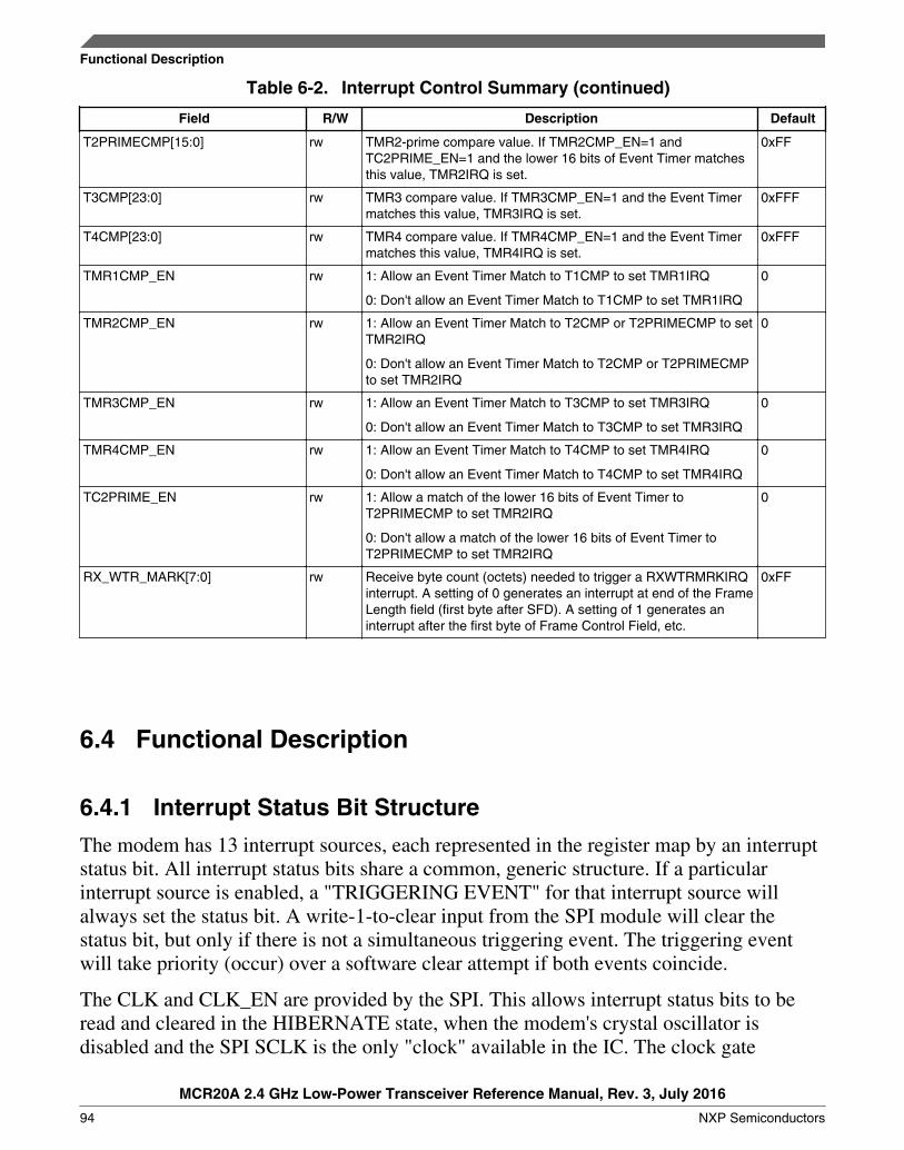
Table 6-2. Interrupt Control Summary (continued)
Field R/W Description Default
T2PRIMECMP[15:0] rw TMR2-prime compare value. If TMR2CMP_EN=1 andTC2PRIME_EN=1 and the lower 16 bits of Event Timer matchesthis value, TMR2IRQ is set.
0xFF
T3CMP[23:0] rw TMR3 compare value. If TMR3CMP_EN=1 and the Event Timermatches this value, TMR3IRQ is set.
0xFFF
T4CMP[23:0] rw TMR4 compare value. If TMR4CMP_EN=1 and the Event Timermatches this value, TMR4IRQ is set.
0xFFF
TMR1CMP_EN rw 1: Allow an Event Timer Match to T1CMP to set TMR1IRQ
0: Don't allow an Event Timer Match to T1CMP to set TMR1IRQ
0
TMR2CMP_EN rw 1: Allow an Event Timer Match to T2CMP or T2PRIMECMP to setTMR2IRQ
0: Don't allow an Event Timer Match to T2CMP or T2PRIMECMPto set TMR2IRQ
0
TMR3CMP_EN rw 1: Allow an Event Timer Match to T3CMP to set TMR3IRQ
0: Don't allow an Event Timer Match to T3CMP to set TMR3IRQ
0
TMR4CMP_EN rw 1: Allow an Event Timer Match to T4CMP to set TMR4IRQ
0: Don't allow an Event Timer Match to T4CMP to set TMR4IRQ
0
TC2PRIME_EN rw 1: Allow a match of the lower 16 bits of Event Timer toT2PRIMECMP to set TMR2IRQ
0: Don't allow a match of the lower 16 bits of Event Timer toT2PRIMECMP to set TMR2IRQ
0
RX_WTR_MARK[7:0] rw Receive byte count (octets) needed to trigger a RXWTRMRKIRQinterrupt. A setting of 0 generates an interrupt at end of the FrameLength field (first byte after SFD). A setting of 1 generates aninterrupt after the first byte of Frame Control Field, etc.
0xFF
6.4 Functional Description
6.4.1 Interrupt Status Bit Structure
The modem has 13 interrupt sources, each represented in the register map by an interruptstatus bit. All interrupt status bits share a common, generic structure. If a particularinterrupt source is enabled, a "TRIGGERING EVENT" for that interrupt source willalways set the status bit. A write-1-to-clear input from the SPI module will clear thestatus bit, but only if there is not a simultaneous triggering event. The triggering eventwill take priority (occur) over a software clear attempt if both events coincide.
The CLK and CLK_EN are provided by the SPI. This allows interrupt status bits to beread and cleared in the HIBERNATE state, when the modem's crystal oscillator isdisabled and the SPI SCLK is the only "clock" available in the IC. The clock gate
Functional Description
MCR20A 2.4 GHz Low-Power Transceiver Reference Manual, Rev. 3, July 2016
94 NXP Semiconductors
guarantees that the status bit sees a clock only when either a triggering event occurs or awrite-1-to-clear pulse arrives from the SPI. This reduces interrupt status bit powerconsumption to an absolute minimum. The common interrupt status bit structure is shownin this figure.
Figure 6-1. Common Interrupt Bit Structure
NOTEFor any modem interrupt source, if the triggering event occurs,the Interrupt Status Bit will be set regardless of the state of thecorresponding MASK bit. If any of the 13 interrupts is to beignored, software should set the corresponding MASK bit andapply the appropriate bit mask when reading the IRQSTS1,IRQSTS2, or IRQSTS3 register to mask out the unwantedstatus bit.
6.4.2 Clearing Interrupts
All interrupt status bits use a write-1-to-clear protocol. Writing a '1' to the interrupt statusbit in any one of the IRQSTS1, IRQSTS2, or IRQSTS3 registers clears the offendinginterrupt. Writing a '0' to an interrupt status bit has no effect on the bit. Interrupt statusbits are not affected by reads.
Chapter 6 Modem: Interrupts
MCR20A 2.4 GHz Low-Power Transceiver Reference Manual, Rev. 3, July 2016
NXP Semiconductors 95
6.4.3 Timer Interrupts
The modem features a 24-bit Event Timer which runs at the 802.15.4 bit rate of 250 kHz.The modem has four timer interrupts (TMR1IRQ, TMR2IRQ, TMR3IRQ, andTMR4IRQ), each with its own 24-bit compare register (T1CMP, T2CMP, T3CMP, andT4CMP) and each with its own compare enable (TMR1CMP_EN, TMR2CMP_EN,TMR3CMP_EN, and TMR4CMP_EN).
For each timer compare enable:
• If the compare enable bit is set - A match on the respective 24-bit compare value tothe Event Timer will cause the corresponding interrupt status bit to become set.
• If the compare enable is low - Event Timer matches will not cause the correspondinginterrupt status bit to become set.
In addition, a 16-bit T2PRIMECMP compare value is provided along with a compare-enable bit TC2PRIME_EN.
• When TC2PRIME_EN is set and TMR2CMP_EN is also set - A match onT2PRIMECMP with the lower 16 bits of Event Timer will cause TMR2IRQ tobecome set rather than a full 24-bit compare.
6.4.4 PLL Unlock Interrupt
The PLL_UNLOCK_IRQ status bit indicates the PLL has come out of lock during a TX,RX or CCA transceiver operation. The modems Sequence Manager will begin monitoringfor PLL unlocks only after a complete transceiver warm-up has occurred; unlocks thatoccur during warm-up will not cause a PLL unlock. A PLL unlock that occurs after thewarm-up period will cause a sequence abort.
6.4.5 Filterfail Interrupt
The modems Packet Processor performs filtering on all received packets to determinewhether the packet is intended for the device based on rules which if violated, will causea Filterfail interrupt. A Filterfail interrupt will occur during packet reception when apacket fails filtering rules. On a Filterfail interrupt, the FILTERFAIL_CODE register canbe read to ascertain more information about the nature of the filter failure.
NOTEA Filterfail interrupt is not expected to be widely used inmission modes; it has been provided primarily for debugpurposes.
Functional Description
MCR20A 2.4 GHz Low-Power Transceiver Reference Manual, Rev. 3, July 2016
96 NXP Semiconductors
NOTEIf a packet is received and First-Stage filtering fails (i.e., one ormore of bits filterfail_code[0-3] is set, the Second-Stagefilterfail_code bits, 3-9, should be ignored since the modem'spacket processor will not know where to search for PAN ID andaddress fields in the incoming byte stream for illegal addressingmodes.
This table indicates each Filterfail code bit and it respective reason the packet wasrejected.
Table 6-3. Filterfail Codes
FILTERFAIL CODE BIT REASON FOR FILTERFAIL
filterfail_code[0] Fails Stage 1 Frame Length Checking (FL < 5 or FL > MAXFRAMELENGTH)
filterfail_code[1] Fails Stage 1 Section 7.2.1.1.6 or Section 7.2.1.1.8 Checking (DST_ADDR_MODE orSRC_ADDR_MODE = 1)
filterfail_code[2] Fails Stage 1 Section 7.2.1.1.5 Checking (Illegal PAN_ID_COMPRESSION Usage)
filterfail_code[3] Fails Stage 1 Frame Version Checking
filterfail_code[4] Fails Stage 2 Auto-RxAck Checking (Illegal Ack Frame Format in Sequence TR)
filterfail_code[5] Fails Stage 2 Frame Type Checking (Incorrect Frame Filter Bit setting)
filterfail_code[6] Fails Stage 2 Frame Length Checking (Illegal Beacon, Data, or Cmd FL)
filterfail_code[7] Fails Stage 2 Addressing Mode Checking (Illegal Addressing Mode for Beacon, Data, or Cmd)
filterfail_code[8] Fails Stage 2 Sequence Number Matching (Sequence TR Only)
filterfail_code[9] Fails Stage 2 PAN ID or Address Checking (Beacon, Data, or Cmd)
6.4.6 RX Watermark Interrupt
During packet reception, a RX Watermark interrupt will occur when the number ofreceived bytes matches the contents of the RX_WTR_MARK register minus 1.
NOTEFor the purpose of defining RX_WTR_MARK, the first bytereceived is the Frame Length field (PHR). The second bytereceived is the least-significant byte of Frame Control Field,etc.
For example, to cause an RX Watermark Interrupt to occur after the 10th received byte,set RX_WTR_MARK=11.
Chapter 6 Modem: Interrupts
MCR20A 2.4 GHz Low-Power Transceiver Reference Manual, Rev. 3, July 2016
NXP Semiconductors 97
6.4.7 CCA Interrupt
The modems Clear Channel Assessment (CCA) has been completed; CCA interruptsoccur at the end of both CCA and Energy Detect (ED) measurement intervals. For TXand Slotted (beacon-enabled networks) TX modes, the CCAIRQ is asserted indicating theCCA determined the channel is busy. The result of the CCA measurement is reportedback to software in the CCA bit of the IRQSTS2 Register. The CCA bit indicates either abusy channel (1) or an idle channel (0).
6.4.8 RX Interrupt
RX interrupts occur at the end of the transceivers RX operation. An RXIRQ incombination with a SEQIRQ is considered a "Data Indication". RX interrupts are notgenerated on packets which fail FCS (CRC check) or fail packet filtering.
To receive a Data Indication (including RXIRQ) on packets which fail CRC, clear theCRC_MSK bit of the PHY_CTR2 register to 0. To inhibit packet filtering and enableData Indication on packets which would otherwise fail packet filtering rules, set thePROMISCUOUS bit of the PHY_CTRL4 register to 1.
6.4.9 TX Interrupt
TX interrupts (TX_IRQ) occur at the end of the transceivers TX operation.
6.4.10 Sequencer Interrupt
The Sequencer Interrupt (SEQIRQ), indicates that an autosequence has completed andthe Sequence Manager has returned to its idle state. A SEQIRQ will always occur at theend of an autosequence even if the autosequence terminated abnormally, such as aSoftware Abort, a TC3 Timeout or a PLL Unlock Abort.
NOTEThe ABORT_STS register can be read to determine which ofthese abnormal terminations occurred, if any (see the registerssection for more details).
The SEQIRQ always occurs whenever the Sequence Manager transitions from non-idleto idle state. When SEQIRQ occurs, software can be sure that the Sequence Manager is inits idle state and a new sequence can be programmed immediately.
Functional Description
MCR20A 2.4 GHz Low-Power Transceiver Reference Manual, Rev. 3, July 2016
98 NXP Semiconductors
6.4.11 Interrupts from Exiting Low Power Modes
The modem has two low power modes which generate an 'Wake' interrupt. A Wakeinterrupt (WAKE_IRQ) occurs from either of these two conditions:
1. Exit from RESET2. Exit from HIBERNATE
A transition out of RESET or HIBERNATE will always cause a WAKE_IRQ whenunmasked. WAKE_IRQ is the only modem interrupt whose default state is "unmasked"so the MCU can expect this interrupt without any prior programming of the device. TheMCU can interpret the WAKE_IRQ interrupt as a "Modem Ready" indication.
6.4.11.1 Exiting from RESET
The modem is put into reset and will stay in reset through the assertion of RST_B (resetbar or RESET). In the interest of lowest power, there is no external pull-up resistor oninput RST_B. As part of the MCU initialization, an internal GPIO is programmed as anoutput and then driven low to reset the modem. The RST_B input is asynchronous andneeds to be held low for only a short period. In the reset condition, the modem is totallypowered down and no clocks are available. Coming out of reset, the WAKE_IRQinterrupt status bit is set and causes an assertion on IRQ_B because WAKE_MSK is 0 bydefault. After the interrupt request is seen by the MCU, the modem is alive and ready forSPI transactions.
6.4.11.2 Exiting from HIBERNATE
The hibernate or low power mode is a specific mode where the XTAL is disabled. TheSPI is capable of operation in modem low power modes, except Reset. Going out ofhibernate mode through SPI means that the XTAL needs to be start up again, the digitalregulator forced to high power mode and a new wake up interrupt (WAKE_IRQ) isgenerated as a result.
Operation in Hibernate mode allows most modem registers and the complete PacketBuffer to be accessed in radio's lowest-power operational state thereby, enabling minimalpower consumption especially during the register-initialization phase of the IC's software.
Chapter 6 Modem: Interrupts
MCR20A 2.4 GHz Low-Power Transceiver Reference Manual, Rev. 3, July 2016
NXP Semiconductors 99
In Hibernate, the SPI operates in "asynchronous mode". To write a register, the SPImodule generates both clock and clock enable to the Register block since the crystaloscillator is disabled; for reads, no latching of read-back data takes place since theoscillator is disabled therefore, read-back data cannot change.
6.4.12 Packet Buffer Error Interrupt
A Packet Buffer Error Interrupt, PB_ERR_IRQ, indicates that a Packet Buffer UnderrunError has occurred. This condition can occur if a SPI burst read access to the PacketBuffer begins before the incoming packet has been completely received and the SPIPacket Buffer read address overtakes the RX demodulator write address.
Packet Buffer data obtained from a SPI transfer which results in a PB_ERR_IRQ hasbeen corrupted and should be discarded. However, the packet contents have not been lost;the PB_ERR_IRQ should be cleared and the SPI transfer should then be restarted.
Functional Description
MCR20A 2.4 GHz Low-Power Transceiver Reference Manual, Rev. 3, July 2016
100 NXP Semiconductors
Chapter 7Modem: Timer Information
7.1 Event Timer BlockThe modem contains an internal Event Timer block that manages system timing.
The Event Timer consists of a prescaler and a 24-bit counter which increment wheneverthe crystal clock is operating (i.e. the modem is not in Hibernate mode). Interrupts to theMCU may be generated when the "current time" of the counter matches several pre-determined values set in registers via SPI write operations. The current time is accessibleat any time via a SPI read operation as well as programmable via a SPI write operation.
The Event Timer provides the following functions:
• Timer to generate current system time
• Interrupt generation at pre-determined system times
• Abort an RX sequence at pre-determined system time
• Latches "timestamp" value during packet reception
• Initiates timer-triggered sequences
7.2 Event Timer Time BaseThe Event Timer's base clock (tmr_clk) is derived from a programmable prescaler that isclocked by the 32 MHz crystal source. The prescaler provides counter input frequenciesfrom 500 kHz down to 15.625 kHz, which sets the granularity and resolution of thecurrent time. The prescaler, and thus the Event Timer only increment when the crystaloscillator is active. The field TMR_PRESCALE[2:0] at Indirect Access Register 0x28establishes the tmr_clk frequency as shown in the following table.
MCR20A 2.4 GHz Low-Power Transceiver Reference Manual, Rev. 3, July 2016
NXP Semiconductors 101
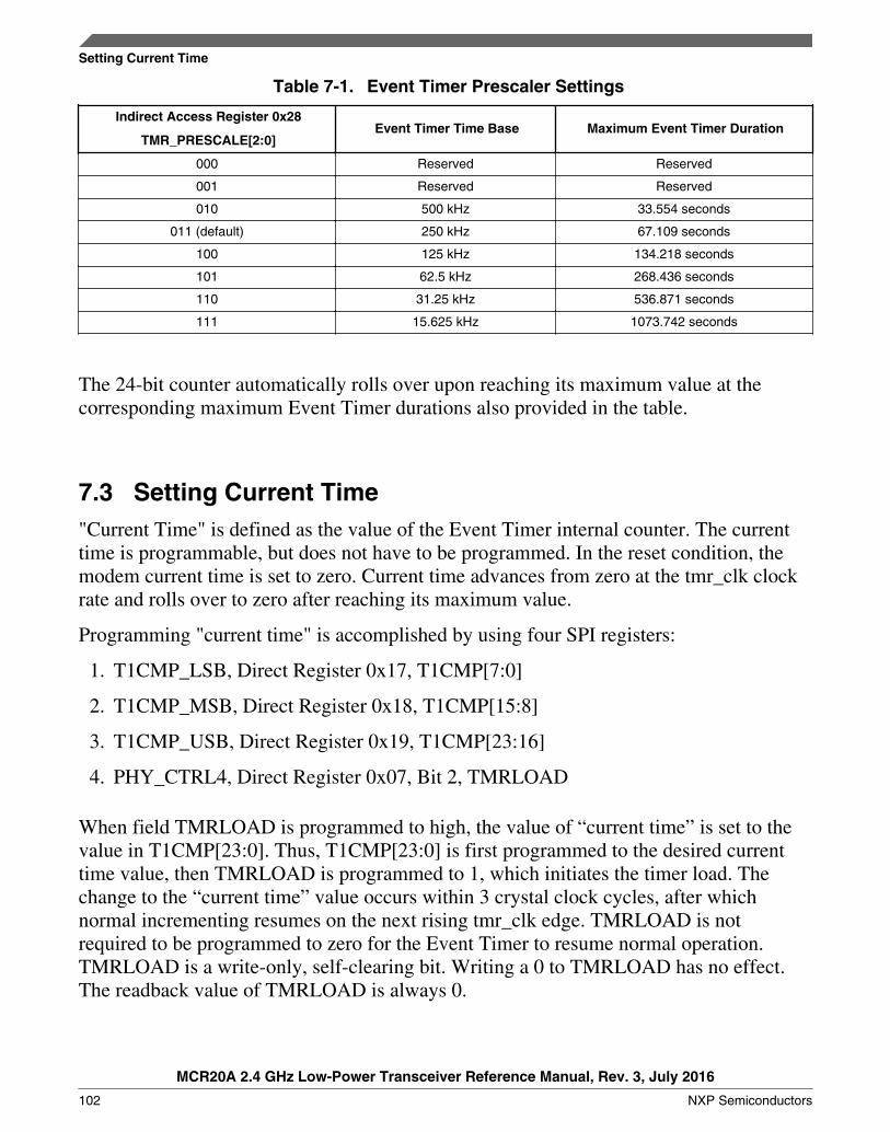
Table 7-1. Event Timer Prescaler Settings
Indirect Access Register 0x28
TMR_PRESCALE[2:0]Event Timer Time Base Maximum Event Timer Duration
000 Reserved Reserved
001 Reserved Reserved
010 500 kHz 33.554 seconds
011 (default) 250 kHz 67.109 seconds
100 125 kHz 134.218 seconds
101 62.5 kHz 268.436 seconds
110 31.25 kHz 536.871 seconds
111 15.625 kHz 1073.742 seconds
The 24-bit counter automatically rolls over upon reaching its maximum value at thecorresponding maximum Event Timer durations also provided in the table.
7.3 Setting Current Time"Current Time" is defined as the value of the Event Timer internal counter. The currenttime is programmable, but does not have to be programmed. In the reset condition, themodem current time is set to zero. Current time advances from zero at the tmr_clk clockrate and rolls over to zero after reaching its maximum value.
Programming "current time" is accomplished by using four SPI registers:
1. T1CMP_LSB, Direct Register 0x17, T1CMP[7:0]
2. T1CMP_MSB, Direct Register 0x18, T1CMP[15:8]
3. T1CMP_USB, Direct Register 0x19, T1CMP[23:16]
4. PHY_CTRL4, Direct Register 0x07, Bit 2, TMRLOAD
When field TMRLOAD is programmed to high, the value of “current time” is set to thevalue in T1CMP[23:0]. Thus, T1CMP[23:0] is first programmed to the desired currenttime value, then TMRLOAD is programmed to 1, which initiates the timer load. Thechange to the “current time” value occurs within 3 crystal clock cycles, after whichnormal incrementing resumes on the next rising tmr_clk edge. TMRLOAD is notrequired to be programmed to zero for the Event Timer to resume normal operation.TMRLOAD is a write-only, self-clearing bit. Writing a 0 to TMRLOAD has no effect.The readback value of TMRLOAD is always 0.
Setting Current Time
MCR20A 2.4 GHz Low-Power Transceiver Reference Manual, Rev. 3, July 2016
102 NXP Semiconductors
7.4 Reading Current TimeThe current value of the Event Timer can be read via the SPI by readingEVENT_TMR_LSB (Direct Register 0x0C) for EVENT_TMR[7:0],EVENT_TMR_MSB (Direct Register 0x0D) for EVENT_TMR[15:8], andEVENT_TMR_USB (Direct Register 0x0E) for EVENT_TMR[23:16].
The “current time” may be obtained using three single-byte SPI reads or a 3-byte SPIburst read (or as part of a longer burst read operation). It is important to realize that theEvent Timer may increment during these SPI read operations or between successive SPIreads if single-byte SPI reads are used. To counter this during such an access, the modemlatches the “current time” to protect the MCU from obtaining an incorrect value. The“current time” most significant 16 bits (MSB, USB) are latched when the least significant8 bits (LSB) SPI location is read. This guarantees a stable value until the MCU completesa read of all 3 bytes constituting the “current time” before it is allowed to update. If suchlatching is undesired, it can be turned off by setting theEVENT_TMR_DO_NOT_LATCH bit to 1. The EVENT_TMR_DO_NOT_LATCH bitresides in the SEQ_MGR_CTRL register (Indirect Access Register 0x3A, bit 3).
NOTE
The preferred procedure to obtain the "current time" value fromthe modem is to perform a 3-byte burst read of the "currenttime" starting at the LSB address.
7.5 Latching the TimestampThe modem has the ability generate a Timestamp, or to latch a copy of the “current time”while continuing to increment its internal counter. This timestamp value latched withinthe Event Timer corresponds to the beginning of a receive packet where the actual packetdata begins after the SFD (Start-of-Frame-Delimiter) has been received. Thetimestamp[23:0] can be accessed via SPI by reading TIMESTAMP_LSB (Direct Register0x0F) for timestamp[7:0], TIMESTAMP_MSB (Direct Register 0x10) fortimestamp[15:8], and TIMESTAMP_USB (Direct Register 0x11) for timestamp[23:16].The timestamp remains latched until another packet is received at which point thetimestamp[23:0] value is updated and re-latched.
Chapter 7 Modem: Timer Information
MCR20A 2.4 GHz Low-Power Transceiver Reference Manual, Rev. 3, July 2016
NXP Semiconductors 103
7.6 Event Timer ComparatorsThe modem incorporates four full 24-bit programmable fields that compare to the EventTimer's "current time". The intent of these compares are to enable the host to scheduleevents relative to the "current time". When a match between the "current time" and anyone of the four timer compare values occurs, a corresponding flag is sent to internalinterrupt logic. This causes the appropriate bit in the IRQSTS3 register (Direct register0x2) to be set and depending on the interrupt mask control bit, generate an interrupt eventon the IRQ_B pin.
7.6.1 Timer Compare Fields
There are four 24-bit timer compare fields and one 16-bit timer compare field:
1. T1CMP[23:0], (T1CMP_LSB, T1CMP_MSB, T1CMP_USB), Direct Address 0x17,0x18, 0x19 respectively.
2. T2CMP[23:0], (T2CMP_LSB, T2CMP_MSB, T2CMP_USB), Direct Address 0x1A,0x1B, 0x1C respectively.
3. T3CMP[23:0], (T3CMP_LSB, T3CMP_MSB, T3CMP_USB), Direct Address 0x12,0x13, 0x14 respectively.
4. T4CMP[23:0], (T4CMP_LSB, T4CMP_MSB, T4CMP_USB), Direct Address 0x1D,0x1E, 0x1F respectively.
Additionally, there is a special 16-bit timer compare field for situations where the upperbyte of EVENT_TMR is a 'don’t care' case.
1. T2PRIMECMP[15:0], (T2PRIMECMP_LSB, T2PRIMECMP_MSB), DirectAddress 0x15 and 0x16 respectively.
The TMR2IRQ status bit can be set by a match to T2CMP or T2PRIMECMP:
• If register bit TC2PRIME_EN=1 (PHY_CTRL4 register, Direct Address 0x7, bit 0),then TMR2IRQ becomes set by a match to T2PRIMECMP (16-bit compare).
• If TC2PRIME_EN=0, then TMR2IRQ becomes set by a match to T2CMP (24-bitcompare).
Event Timer Comparators
MCR20A 2.4 GHz Low-Power Transceiver Reference Manual, Rev. 3, July 2016
104 NXP Semiconductors
7.6.2 Timer Compare-Enable Bits
Each timer comparator has a enable bit that enables or disables the compare function. Toenable, write a “1” to the corresponding comparator. The default condition is the timerdisabled (reset to “0”):
1. TMR1CMP_EN, PHY_CTRL3 Register, Direct Address 0x05, bit 4
2. TMP2CMP_EN, PHY_CTRL3 Register, Direct Address 0x05, bit 5
3. TMR3CMP_EN, PHY_CTRL3 Register, Direct Address 0x05, bit 6
4. TMR4CMP_EN, PHY_CTRL3 Register, Direct Address 0x05, bit 7
If a timer comparator is enabled using its associated bit, the corresponding interrupt statusbit (TMRxIRQ) will be set by a timer compare match to its respective TxCMP register. Ifa timer comparator is disabled using its associated bit, the corresponding interrupt statusbit (TMRxIRQ) will not be set by a timer compare match to its respective TxCMPregister.
7.6.3 Timer Interrupt Status Bits
When enabled, all four fields can be continuously compared to the current value of theEvent Timer counter. When a match occurs, the following corresponding internal statusflags assert:
1. TMR1IRQ, IRQSTS3 Register, Direct Address 0x02, bit 0
2. TMR2IRQ, IRQSTS3 Register, Direct Address 0x02, bit 1
3. TMR3IRQ, IRQSTS3 Register, Direct Address 0x02, bit 2
4. TMR4IRQ, IRQSTS3 Register, Direct Address 0x02, bit 3
The four interrupt status bits are write-1-to-clear. The status bit remains set until a 1 iswritten to the bit location in the IRQSTS3 register. Writing 0 to the bit or reading the bitwill not change its state.
7.6.4 Timer Interrupt Masks
When a comparator match occurs and the internal status flag asserts, the followinginterrupt masks can enable an interrupt on the IRQ pin:
Chapter 7 Modem: Timer Information
MCR20A 2.4 GHz Low-Power Transceiver Reference Manual, Rev. 3, July 2016
NXP Semiconductors 105
1. TMR1MSK, IRQSTS3 Register, Direct Address 0x02, bit 4
2. TMR2MSK, IRQSTS3 Register, Direct Address 0x02, bit 5
3. TMR3MSK, IRQSTS3 Register, Direct Address 0x02, bit 6
4. TMR4MSK, IRQSTS3 Register, Direct Address 0x02, bit 7
If the interrupt mask is set to “1” (masked), the respective interrupt status bit, TMRxIRQ,will not cause an interrupt on the IRQ_B pin. If the interrupt mask is set to “0” (enabled),the respective interrupt status bit, TMRxIRQ, will cause an interrupt on the IRQ_B pin.Timer mask bits, TMRxMSK, have no effect on the state of the TMRxIRQ interruptstatus bits; they only allow (or prevent) the respective TMRxIRQ bit from generating aninterrupt on IRQ_B.
7.6.5 Setting Compare Values
Because the primary timer compare fields are 24-bit values, they are each shared across 3sequential SPI register addresses. The timer compare value can be changed using 3single-byte SPI writes, one 3-byte SPI burst write or as part of a longer multi-byte writeoperation.
Note
Not all bits of the timer compare value are updatedsimultaneously by the SPI. To prevent the Event Timer fromgenerating a false match to a partially updated timer comparevalue, software should clear the respective TMRxCMP_EN bitprior to changing the timer compare register TxCMP. OnceTxCMP has been updated, software can re-enable the respectiveTMRxCMP_EN bit.
7.7 Intended Event Timer UsageIt is intended that the system use the "current time" value and the timer comparefunctions of the Event Timer to schedule system events, including:
• Generating time-based interrupts
• Abort an RX operation
• Triggering transceiver operations
Intended Event Timer Usage
MCR20A 2.4 GHz Low-Power Transceiver Reference Manual, Rev. 3, July 2016
106 NXP Semiconductors
7.7.1 Generating Time-Based Interrupts
Generating time-based interrupts is accomplished by setting timer compare valuesrelative to the "current time" allowing the Event Timer counter to increment until a timercompare match is generated, and using this match to generate an interrupt to the host. Thegeneral procedure is as follows:
1. Disable the timer compare.
2. Enable the timer compare interrupt mask.
3. Read the "current time" value from event_tmr[23:0].
4. Add an offset to the "current time" value to equal the desired "future time".
5. Program the appropriate timer_compare value (TxCMP) to "future time".
6. Program the appropriate TMRxCMP_EN bit to enable the compare.
7. Allow a timer compare match to set the status register bit and generate an interrupt(see the Timer Interrupt Status Bits section). The appropriate internal status registerbit is always set upon a TxCMP match. An external interrupt is generated when thecorresponding SPI interrupt mask bit, TMRxMSK, is clear.
8. Program the appropriate TMRxCMP_EN bit to disable the compare function. If thisis not done, the compare function will continue to run and generate another interruptevery time the counter rolls over and again matches the comparator.
7.7.2 Using T3CMP to Abort an RX operation
The Event Timer provides a timer-based mechanism to automatically abort an RXoperation. The modem is put into an RX operation when XCVSEQ[2:0] (PHY_CTRL1register, Direct Address 0x03) is set to 0x01. An RX autosequence will commence andwill begin a search for preamble. Software can program, in advance, a hardware timeoutto occur such that the RX autosequence can be automatically aborted by hardware after acertain amount of time elapses without a packet being detected.
The general procedure is as follows:
1. Read the “current time” value from EVENT_TMR[23:0].
2. Add an offset to the “current time” value to equal desired “future time” to abort theRX operation.
Chapter 7 Modem: Timer Information
MCR20A 2.4 GHz Low-Power Transceiver Reference Manual, Rev. 3, July 2016
NXP Semiconductors 107
3. Program register T3CMP[23:0] to value “future time”.
4. Program TC3TMOUT, (PHY_CTRL4 Register, Direct Address 0x07, bit 6) to 1, toenable the hardware aborting of the RX operation.
5. Program XCVSEQ=1, to start the RX autosequence.
6. When “current time” equals T3CMP[23:0], the modem aborts the RX autosequenceand the Sequence Manager returns to SEQ_IDLE state. The SEQIRQ interrupt statusbit (IRQSTS1 Register, Direct Address 0, bit 0) will be set, and the TMR3IRQinterrupt status bit will also be set. The RXIRQ interrupt status bit (IRQSTS1 DirectAddress 0, bit 2) will not be set since no packet was received before the timeout.
7.7.3 Using T2CMP or T2PRIMECMP to Trigger TransceiverOperations
The Event Timer provides a timer-based mechanism to automatically launch a transceiverautosequence. Using this method, a sequence can be “scheduled” for time in the future,and the MCU can be put into a reduced power state, without the need to wake up at theappropriate time to start the autosequence.
The general procedure is as follows:
1. Read the “current time” value from EVENT_TMR[23:0].
2. Add an offset to the “current time” value to equal desired “future time” to launch theautosequence.
3. For either a 24-bit or a 16-bit compare:
• For a 24-bit compare: program register T2CMP[23:0] to value “future time”, andset TC2PRIME_EN=0.
• For a 16-bit compare: program register T2PRIMECMP[15:0] to value “futuretime”, and set TC2PRIME_EN=1.
4. Set TMRTRIGEN=1 and program the desired autosequence into XCVSEQ[2:0].Both TMRTRIGEN and XCVSEQ fields reside in the PHY_CTRL1 register (DirectAddress 0x03).
5. When “current time” equals T2CMP[23:0] (for a 24-bit compare), orT2PRIMECMP[15:0] (for a 16-bit compare), the modem will launch the scheduledautosequence in accordance with the XCVSEQ[2:0] field. The TMR2IRQ interruptstatus bit will become set.
Intended Event Timer Usage
MCR20A 2.4 GHz Low-Power Transceiver Reference Manual, Rev. 3, July 2016
108 NXP Semiconductors

6. The MCU can wake up at this point (if TMR2MSK=0), or can elect to continue inlow-power mode until the autosequence completes, at which time SEQIRQ willbecome set. If SEQMSK=0, then SEQIRQ will interrupt the MCU at the completionof the transceiver operation.
Chapter 7 Modem: Timer Information
MCR20A 2.4 GHz Low-Power Transceiver Reference Manual, Rev. 3, July 2016
NXP Semiconductors 109

Intended Event Timer Usage
MCR20A 2.4 GHz Low-Power Transceiver Reference Manual, Rev. 3, July 2016
110 NXP Semiconductors
Chapter 8Modem SPI Interface
8.1 Modem SPI OverviewThe modem's SPI interface allows an MCU to communicate with the modem's register setand Packet Buffer. The modem's SPI is a slave-only interface; the MCU must driveR_SSEL_B, R_SCLK and R_MOSI. Write and read access to both Direct and Indirectregisters is supported, and transfer length can be single-byte, or bursts of unlimitedlength. Write and read access to the Packet buffer can also be single-byte, or a burst modeof unlimited length. The modem's SPI interface is asynchronous to the rest of the IC. Norelationship between R_SCLK and the modem's internal oscillator is assumed. And norelationship between R_SCLK and the CLK_OUT pin is assumed. All synchronization ofthe SPI interface to the modem IC takes place inside the SPI module, alleviating theburden on other block designers to provide this synchronization internal to their modules.SPI synchronization takes place in both directions: SPI-to-IC (register writes), and IC-to-SPI (register reads). The SPI is capable of operation in all modem Power Modes, exceptReset. Operation in Hibernate mode allows most modem registers, and the completePacket Buffer, to be accessed in the modem's lowest-power operational state, enablingminimal power consumption, especially during the register-initialization phase of the IC.The SPI design features a compact, single-byte control word, reducing SPI access latencyto a minimum. Most SPI access types require only a single-byte control word, with theaddress embedded in the control word. During control word transfer (the first byte of anySPI access), the contents of the IRQSTS1 register (the modem's highest-priority statusregister) are are always shifted out, so that the MCU gets access to IRQSTS1, with theminimum possible latency, on every SPI access.
8.2 Modem SPI Basic OperationThe modem operates as a SPI slave only. The microcontroller supplies the interface clockand acts as SPI master.
MCR20A 2.4 GHz Low-Power Transceiver Reference Manual, Rev. 3, July 2016
NXP Semiconductors 111
SPI Pin Definition
8.2.1.1 Radio Select SEL (R_SSEL_B)
The MCU Master SPI selects and activates the modem's Slave SPI by assertingR_SSEL_B (low).
8.2.1.2 Radio SPI Clock (R_SCLK)
The MCU Master SPI provides a serial bit clock to the modem's Slave SPI on R_SCLK.
8.2.1.3 Radio MOSI - Master Data Out Slave Data In (R_MOSI)
The MCU Master SPI transmits Control, Address and Write data to the modem's SPISlave on R_MOSI.
8.2.1.4 Radio MISO - Master Data In, Slave Data Out (R_MISO)
The modem's Slave SPI transmits readback data to the MCU Master SPI on R_MISO.
8.2.1.4.1 Setting R_MISO Off Impedance
MISO_HIZ_EN - Determines the output state of the modem's R_MISO output whenR_SSEL_B is deasserted (high).
1: R_MISO output is tristated (default)
0: R_MISO output is driven low by the SPI slave
8.2.1.4.2 R_MISO Pull-up Requirement
Because the modem tri states its R_MISO output when a SPI transfer is not in progress(R_SSEL_B deasserted), a pull-up is required to ensure that the SPI Master does not see afloating MISO input.
In a configuration consisting of only a single Master (MCU) and single Slave (themodem), this pull-up can be an internal pull-up on the MCU's MISO input. Moreover,after initialization, the modem's MISO_HIZ_EN bit can be cleared (enabling the modemto drive R_MISO at all times), and the MCU pull-up can be disabled.
8.2.1
SPI Pin Definition
MCR20A 2.4 GHz Low-Power Transceiver Reference Manual, Rev. 3, July 2016
112 NXP Semiconductors
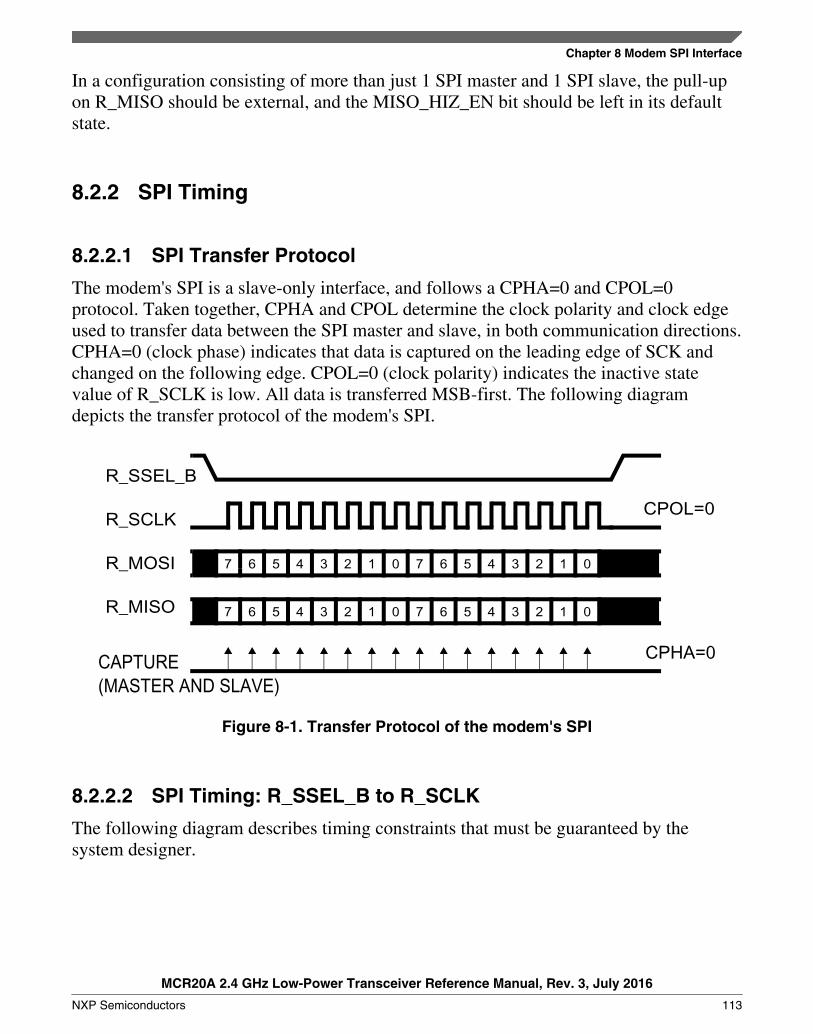
In a configuration consisting of more than just 1 SPI master and 1 SPI slave, the pull-upon R_MISO should be external, and the MISO_HIZ_EN bit should be left in its defaultstate.
SPI Timing
8.2.2.1 SPI Transfer Protocol
The modem's SPI is a slave-only interface, and follows a CPHA=0 and CPOL=0protocol. Taken together, CPHA and CPOL determine the clock polarity and clock edgeused to transfer data between the SPI master and slave, in both communication directions.CPHA=0 (clock phase) indicates that data is captured on the leading edge of SCK andchanged on the following edge. CPOL=0 (clock polarity) indicates the inactive statevalue of R_SCLK is low. All data is transferred MSB-first. The following diagramdepicts the transfer protocol of the modem's SPI.
R_SSEL_B
R_SCLK
R_MOSI
R_MISO
CAPTURE(MASTER AND SLAVE)
CPOL=0
7
7 6 5 4 3 2 1 0 7 6 5 4 3 2 1 0
6 5 4 3 2 1 0 7 6 5 4 3 2 1 0
CPHA=0
Figure 8-1. Transfer Protocol of the modem's SPI
8.2.2.2 SPI Timing: R_SSEL_B to R_SCLK
The following diagram describes timing constraints that must be guaranteed by thesystem designer.
8.2.2
Chapter 8 Modem SPI Interface
MCR20A 2.4 GHz Low-Power Transceiver Reference Manual, Rev. 3, July 2016
NXP Semiconductors 113
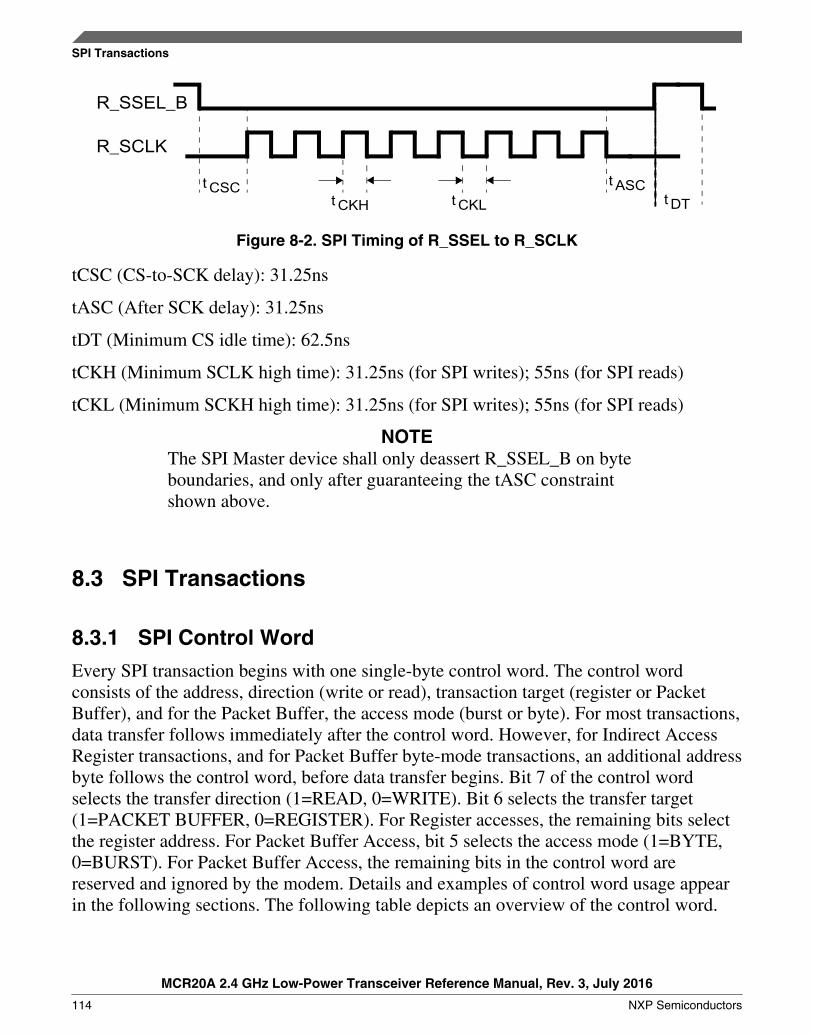
R_SSEL_B
R_SCLK
t CSC t ASCt DTt CKLt CKH
Figure 8-2. SPI Timing of R_SSEL to R_SCLK
tCSC (CS-to-SCK delay): 31.25ns
tASC (After SCK delay): 31.25ns
tDT (Minimum CS idle time): 62.5ns
tCKH (Minimum SCLK high time): 31.25ns (for SPI writes); 55ns (for SPI reads)
tCKL (Minimum SCKH high time): 31.25ns (for SPI writes); 55ns (for SPI reads)
NOTEThe SPI Master device shall only deassert R_SSEL_B on byteboundaries, and only after guaranteeing the tASC constraintshown above.
SPI Transactions
8.3.1 SPI Control Word
Every SPI transaction begins with one single-byte control word. The control wordconsists of the address, direction (write or read), transaction target (register or PacketBuffer), and for the Packet Buffer, the access mode (burst or byte). For most transactions,data transfer follows immediately after the control word. However, for Indirect AccessRegister transactions, and for Packet Buffer byte-mode transactions, an additional addressbyte follows the control word, before data transfer begins. Bit 7 of the control wordselects the transfer direction (1=READ, 0=WRITE). Bit 6 selects the transfer target(1=PACKET BUFFER, 0=REGISTER). For Register accesses, the remaining bits selectthe register address. For Packet Buffer Access, bit 5 selects the access mode (1=BYTE,0=BURST). For Packet Buffer Access, the remaining bits in the control word arereserved and ignored by the modem. Details and examples of control word usage appearin the following sections. The following table depicts an overview of the control word.
8.3
SPI Transactions
MCR20A 2.4 GHz Low-Power Transceiver Reference Manual, Rev. 3, July 2016
114 NXP Semiconductors
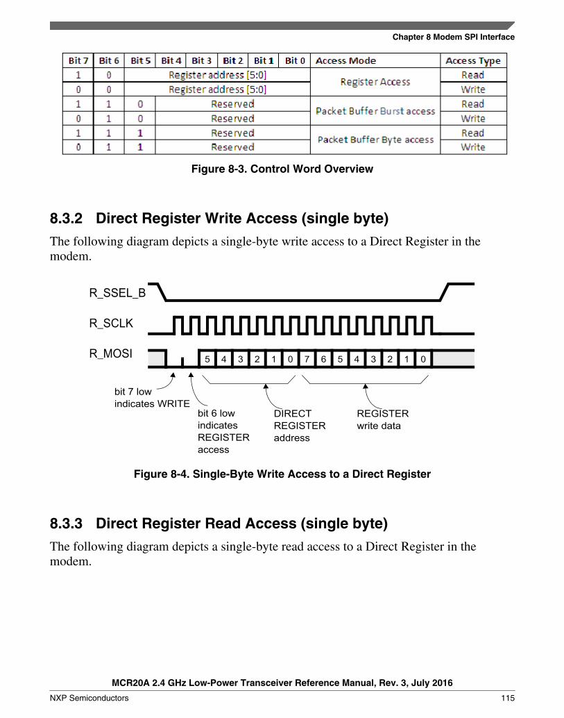
Figure 8-3. Control Word Overview
8.3.2 Direct Register Write Access (single byte)
The following diagram depicts a single-byte write access to a Direct Register in themodem.
R_SSEL_B
R_SCLK
R_MOSI 5 4 3 2 1 0 7 6 5 4 3 2 1 0
bit 7 lowindicates WRITE
bit 6 lowindicatesREGISTERaccess
DIRECTREGISTERaddress
REGISTERwrite data
Figure 8-4. Single-Byte Write Access to a Direct Register
8.3.3 Direct Register Read Access (single byte)
The following diagram depicts a single-byte read access to a Direct Register in themodem.
Chapter 8 Modem SPI Interface
MCR20A 2.4 GHz Low-Power Transceiver Reference Manual, Rev. 3, July 2016
NXP Semiconductors 115
R_SSEL_B
R_SCLK
R_MOSI
R_MISO
5 4 3 2 1 0
bit 7 highindicatesREAD DIRECT
REGISTERaddress
REGISTERread data
7 6 5 4 3 2 1 0
bit 6 highindicatesREGISTERaccess
Figure 8-5. Single-Byte read Access to a Direct Register
8.3.4 Direct Register Write Access (multi byte)
The following diagram depicts a multi-byte write access to Direct Register space in themodem.
R_SSEL_B
R_SCLK
R_MOSI 5 4 3 2 1 0 7 6 5 4 3 2 1 0
bit 7 lowindicates WRITE
bit 6 lowindicatesREGISTERaccess
DIRECTREGISTERaddress “N”
REGISTER “N”write data
7 6 5 4 3 2 1 0
REGISTER “N+1”write data
Figure 8-6. Multi-Byte Write Access to a Direct Register Space
8.3.5 Direct Register Read Access (multi byte)
The following diagram depicts a multi-byte read access to Direct Register space in themodem.
SPI Transactions
MCR20A 2.4 GHz Low-Power Transceiver Reference Manual, Rev. 3, July 2016
116 NXP Semiconductors
R_SSEL_B
R_SCLK
R_MOSI
R_MISO
5 4 3 2 1 0
bit 7 highindicates READ DIRECT
REGISTERaddress
REGISTER “N”read data
7 6 5 4 3 2 1 0 7 6 5 4 3 2 1 0
REGISTER “N+1”read data
bit 6 lowindicatesREGISTERaccess
Figure 8-7. Multi-Byte Read Access to a Direct Register Space
8.3.6 Indirect Register Write Access (multi byte)
The following diagram depicts a multi-byte write access to Indirect Register space in themodem.
R_SSEL_B
R_SCLK
R_MOSI 7 6 5 4 3 2 1 0
bit 7 lowindicates WRITE bit 6 low
indicatesREGISTERaccess
IAR INDEXREGISTER(address 0x3E)
IAR REGISTER “N”address
7 6 5 4 3 2 1 0
IAR REGISTER “N”write data
111 011
IAR REGISTER “N+1”write data
Figure 8-8. Multi-Byte Write Access to an Indirect Register Space
NOTEMulti-byte SPI transactions to an Indirect Address space are notpermitted in Hibernate state. Use single-byte transactions only.
Chapter 8 Modem SPI Interface
MCR20A 2.4 GHz Low-Power Transceiver Reference Manual, Rev. 3, July 2016
NXP Semiconductors 117
8.3.7 Indirect Register Read Access (multi byte)
The following diagram depicts a multi-byte read access to Indirect Register space in themodem.
R_SSEL_B
R_SCLK
R_MOSI
R_MISO
1 1 1 1 01
bit 7 highindicates READ
IAR INDEXREGISTER(address 0x3E)
IAR REGISTER “N”address
7 6 5 4 3 2 1 0
7 6 5 4 3 2 1 0
IAR REGISTER “N”read data
IAR REGISTER “N+1”read data
bit 6 lowindicatesREGISTERaccess
Figure 8-9. Multi-Byte Read Access to an Indirect Register Space
NOTEMulti-byte SPI transactions to Indirect Address space are notpermitted in Hibernate state. Use single-byte transactions only.
8.3.8 Synchronous and Asynchronous Operating Modes
The SPI module is designed to be fully operational in all modem power states, exceptreset. Operation in the Hibernate state means the modem's crystal oscillator is disabled.Most modem registers, direct and indirect, can be accessed, both read and write, duringHibernateIn all non-Hibernate states, the SPI operates in "synchronous mode"; to write aregister, the SPI module generates a clock enable to the Register block, where the enableis used to gate the 32MHz oscillator to each individual register; for reads, the readbackdata is registered using the 32MHz clock at the end of the SPI address phase, so thatreadback data cannot change during shift-out on R_MISO. In Hibernate, the SPI operatesin "asynchronous mode"; to write a register, the SPI module generates both clock andclock enable to the Register block (because the crystal oscillator is disabled); for reads,no latching of readback data takes place, since the oscillator is disabled, readback datacannot change.
SPI Transactions
MCR20A 2.4 GHz Low-Power Transceiver Reference Manual, Rev. 3, July 2016
118 NXP Semiconductors
The SPI module automatically determines its operating state, based on the xtal_readysignal from the crystal oscillator. This signal is captured by the SPI module during theSPI address phase, during the first R_SCLK period. If it is high, the SPI operates insynchronous mode (as described above) for the duration of the SPI transaction. Ifxtal_ready is captured low, the SPI operates in asynchronous mode (as described above)for the duration of the SPI transaction. The transaction ends when R_SSEL_B isdeasserted.
Transitions on xtal_ready are triggered by a SPI write access to the PWR_MODESregister. A SPI write to clear the XTALEN bit of the PWR_MODES register will causean immediate high-to-low transition of xtal_ready; this transition occurs at the end of theSPI transfer, after the last data bit is shifted in on R_MOSI. No further registers can bewritten during this transfer, even if the transaction is multi-byte, because thePWR_MODES registers is at the end of Direct Address space. A SPI write to set theXTALEN bit of PWR_MODES register will cause a delayed low-to-high transition onxtal_ready, because there is a finite crystal warm-up time. The SPI module will continueto operate in asynchronous mode, until a new SPI transaction starts with xtal_readyasserted.
8.3.9 Shifting Out IRQSTS1 During Control Word
During each SPI transaction, while the control word is being shifted in on R_MOSI (SPIaddress phase), the SPI module always shifts out the contents of Direct Register 0"IRQSTS1" on R_MISO. The IRQSTS1 register is the highest-priority register in themodem; it contains the transceiver interrupt status bits, and must be accessed with lowlatency on any 802.15.4 interrupt. Because multiple registers must be accessed ontransceiver interrupts, Direct Register space has been designed to put the highest-priorityregisters at the beginning of address space. A single, multi-byte transfer can be performedto access all of these registers. For such interrupt-driven SPI transfers, software can takeadvantage of the automatic shifting of IRQSTS1 during the SPI address phase, byprogramming a multi-byte SPI transfer to begin at Address 1 (not Address 0), becauseAddress 0 data is provided "for free" on R_MISO during the control word phase. Thus, a7-byte SPI transfer (to read Direct Registers 0 through 6) would require only 7 x 8 = 56SPI clock periods, instead of 64 clock periods, which would be the case if Register 0 hadto be addressed explicitly during such a transaction. The following diagram depicts thelatency advantage that can be gained using this approach.
Chapter 8 Modem SPI Interface
MCR20A 2.4 GHz Low-Power Transceiver Reference Manual, Rev. 3, July 2016
NXP Semiconductors 119
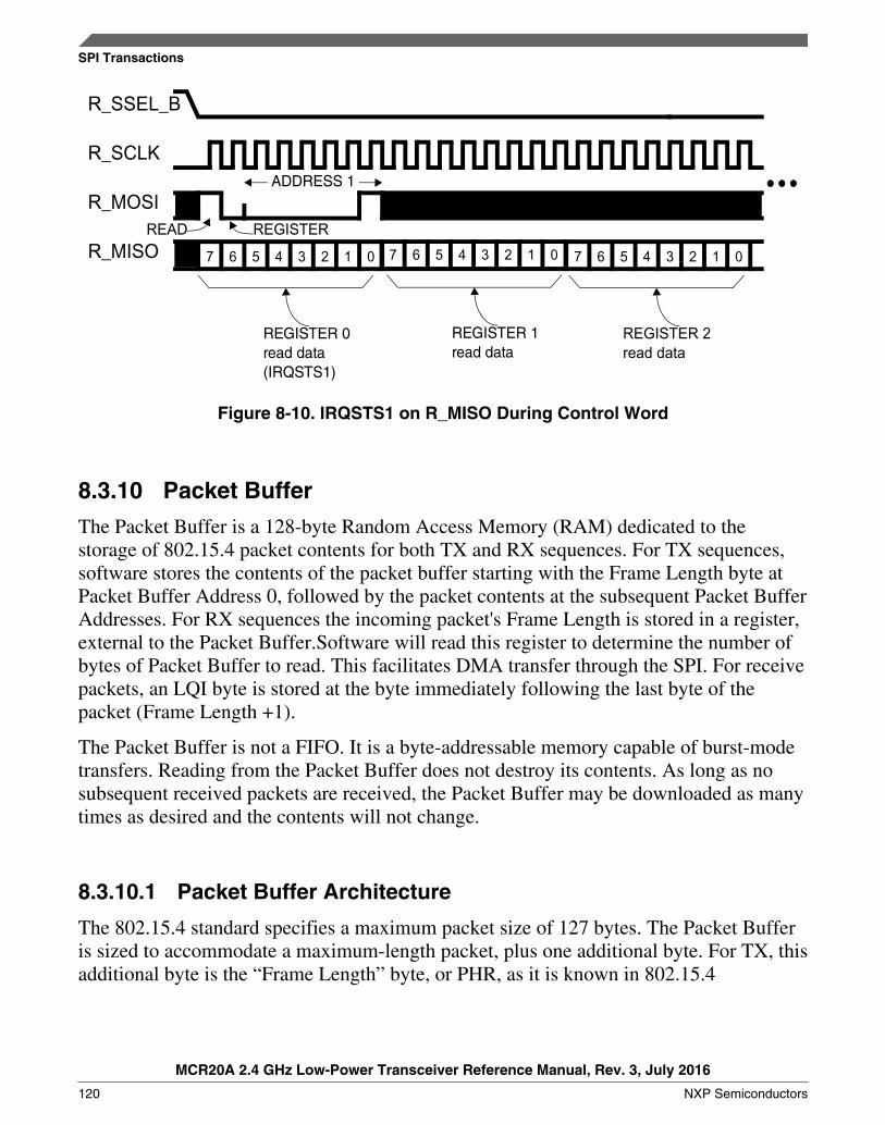
R_SSEL_B
R_SCLK
R_MOSI
R_MISOREGISTER
REGISTER 1read data
READ 7 6 5 4 3 2 1 0 7 6 5 4 3 2 1 0
REGISTER 2read data
ADDRESS 1
7 6 5 4 3 2 1 0
REGISTER 0read data(IRQSTS1)
Figure 8-10. IRQSTS1 on R_MISO During Control Word
8.3.10 Packet Buffer
The Packet Buffer is a 128-byte Random Access Memory (RAM) dedicated to thestorage of 802.15.4 packet contents for both TX and RX sequences. For TX sequences,software stores the contents of the packet buffer starting with the Frame Length byte atPacket Buffer Address 0, followed by the packet contents at the subsequent Packet BufferAddresses. For RX sequences the incoming packet's Frame Length is stored in a register,external to the Packet Buffer.Software will read this register to determine the number ofbytes of Packet Buffer to read. This facilitates DMA transfer through the SPI. For receivepackets, an LQI byte is stored at the byte immediately following the last byte of thepacket (Frame Length +1).
The Packet Buffer is not a FIFO. It is a byte-addressable memory capable of burst-modetransfers. Reading from the Packet Buffer does not destroy its contents. As long as nosubsequent received packets are received, the Packet Buffer may be downloaded as manytimes as desired and the contents will not change.
8.3.10.1 Packet Buffer Architecture
The 802.15.4 standard specifies a maximum packet size of 127 bytes. The Packet Bufferis sized to accommodate a maximum-length packet, plus one additional byte. For TX, thisadditional byte is the “Frame Length” byte, or PHR, as it is known in 802.15.4
SPI Transactions
MCR20A 2.4 GHz Low-Power Transceiver Reference Manual, Rev. 3, July 2016
120 NXP Semiconductors
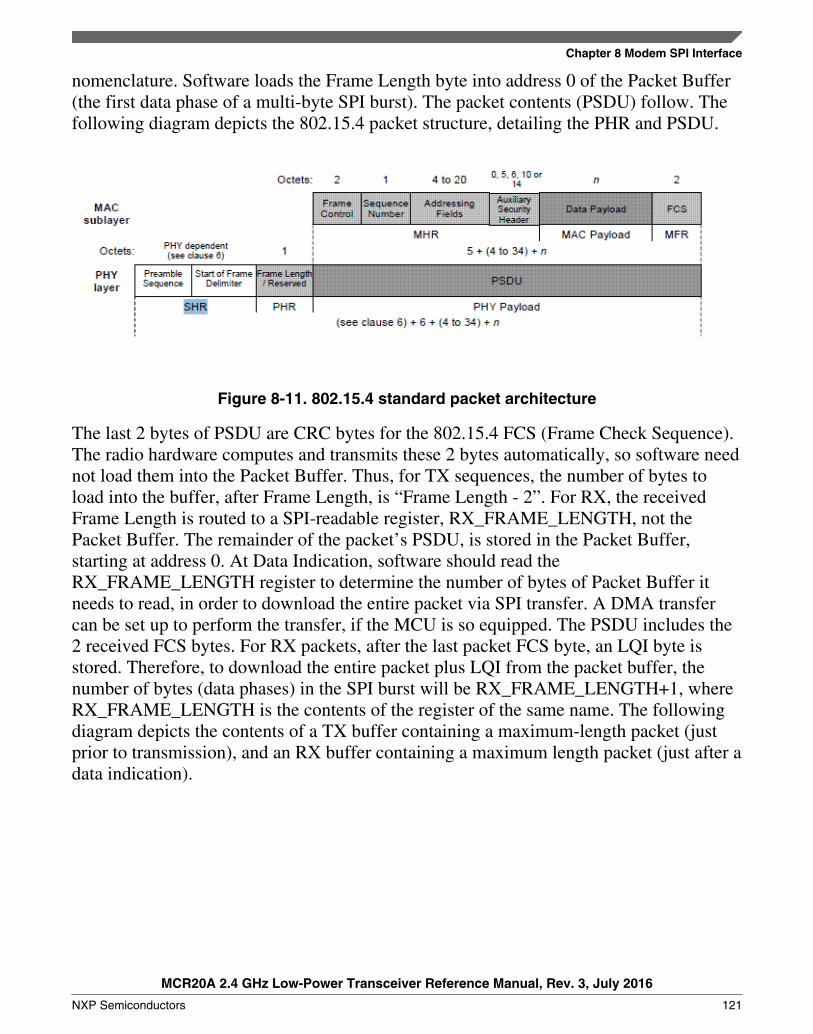
nomenclature. Software loads the Frame Length byte into address 0 of the Packet Buffer(the first data phase of a multi-byte SPI burst). The packet contents (PSDU) follow. Thefollowing diagram depicts the 802.15.4 packet structure, detailing the PHR and PSDU.
Figure 8-11. 802.15.4 standard packet architecture
The last 2 bytes of PSDU are CRC bytes for the 802.15.4 FCS (Frame Check Sequence).The radio hardware computes and transmits these 2 bytes automatically, so software neednot load them into the Packet Buffer. Thus, for TX sequences, the number of bytes toload into the buffer, after Frame Length, is “Frame Length - 2”. For RX, the receivedFrame Length is routed to a SPI-readable register, RX_FRAME_LENGTH, not thePacket Buffer. The remainder of the packet’s PSDU, is stored in the Packet Buffer,starting at address 0. At Data Indication, software should read theRX_FRAME_LENGTH register to determine the number of bytes of Packet Buffer itneeds to read, in order to download the entire packet via SPI transfer. A DMA transfercan be set up to perform the transfer, if the MCU is so equipped. The PSDU includes the2 received FCS bytes. For RX packets, after the last packet FCS byte, an LQI byte isstored. Therefore, to download the entire packet plus LQI from the packet buffer, thenumber of bytes (data phases) in the SPI burst will be RX_FRAME_LENGTH+1, whereRX_FRAME_LENGTH is the contents of the register of the same name. The followingdiagram depicts the contents of a TX buffer containing a maximum-length packet (justprior to transmission), and an RX buffer containing a maximum length packet (just after adata indication).
Chapter 8 Modem SPI Interface
MCR20A 2.4 GHz Low-Power Transceiver Reference Manual, Rev. 3, July 2016
NXP Semiconductors 121
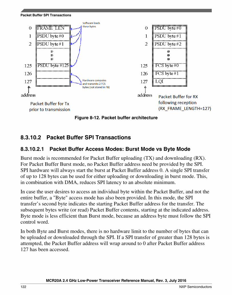
Figure 8-12. Packet buffer architecture
Packet Buffer SPI Transactions
8.3.10.2.1 Packet Buffer Access Modes: Burst Mode vs Byte Mode
Burst mode is recommended for Packet Buffer uploading (TX) and downloading (RX).For Packet Buffer Burst mode, no Packet Buffer address need be provided by the SPI.SPI hardware will always start the burst at Packet Buffer address 0. A single SPI transferof up to 128 bytes can be used for either uploading or downloading in burst mode. This,in combination with DMA, reduces SPI latency to an absolute minimum.
In case the user desires to access an individual byte within the Packet Buffer, and not theentire buffer, a "Byte" access mode has also been provided. In this mode, the SPItransfer’s second byte indicates the starting Packet Buffer address for the transfer. Thesubsequent bytes write (or read) Packet Buffer contents, starting at the indicated address.Byte mode is less efficient than Burst mode, because an address byte must follow the SPIcontrol word.
In both Byte and Burst modes, there is no hardware limit to the number of bytes that canbe uploaded or downloaded through the SPI. If a SPI transfer of greater than 128 bytes isattempted, the Packet Buffer address will wrap around to 0 after Packet Buffer address127 has been accessed.
8.3.10.2
Packet Buffer SPI Transactions
MCR20A 2.4 GHz Low-Power Transceiver Reference Manual, Rev. 3, July 2016
122 NXP Semiconductors
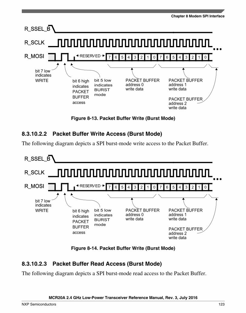
R_SSEL_B
R_SCLK
R_MOSI 7 6 5 4 3 2 1 0
bit 7 lowindicates WRITE bit 6 high
indicates PACKETBUFFERaccess
RESERVED 7 6 5 4 3 2 1 0
PACKET BUFFERaddress 0write data
PACKET BUFFERaddress 1write data
PACKET BUFFERaddress 2write data
bit 5 lowindicatesBURST mode
Figure 8-13. Packet Buffer Write (Burst Mode)
8.3.10.2.2 Packet Buffer Write Access (Burst Mode)
The following diagram depicts a SPI burst-mode write access to the Packet Buffer.
R_SSEL_B
R_SCLK
R_MOSI 7 6 5 4 3 2 1 0
bit 7 lowindicates WRITE bit 6 high
indicates PACKETBUFFERaccess
RESERVED 7 6 5 4 3 2 1 0
PACKET BUFFERaddress 0write data
PACKET BUFFERaddress 1write data
PACKET BUFFERaddress 2write data
bit 5 lowindicatesBURST mode
Figure 8-14. Packet Buffer Write (Burst Mode)
8.3.10.2.3 Packet Buffer Read Access (Burst Mode)
The following diagram depicts a SPI burst-mode read access to the Packet Buffer.
Chapter 8 Modem SPI Interface
MCR20A 2.4 GHz Low-Power Transceiver Reference Manual, Rev. 3, July 2016
NXP Semiconductors 123
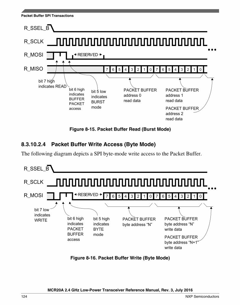
R_SSEL_B
R_SCLK
R_MOSI
bit 7 highindicates READ
R_MISO 7 6 5 4 3 2 1 0
PACKET BUFFERaddress 0read data
PACKET BUFFERaddress 2read data
PACKET BUFFERaddress 1read data
7 6 5 4 3 2 1 0
RESERVED
bit 5 lowindicatesBURSTmode
bit 6 highindicatesBUFFERPACKETaccess
Figure 8-15. Packet Buffer Read (Burst Mode)
8.3.10.2.4 Packet Buffer Write Access (Byte Mode)
The following diagram depicts a SPI byte-mode write access to the Packet Buffer.
R_SSEL_B
R_SCLK
R_MOSI 7 6 5 4 3 2 1 0
bit 7 lowindicatesWRITE PACKET BUFFER
byte address “N”
7 6 5 4 3 2 1 0
PACKET BUFFERbyte address “N”write data
PACKET BUFFERbyte address “N+1”write data
RESERVED
bit 5 highindicatesBYTEmode
bit 6 highindicatesPACKET BUFFERaccess
Figure 8-16. Packet Buffer Write (Byte Mode)
Packet Buffer SPI Transactions
MCR20A 2.4 GHz Low-Power Transceiver Reference Manual, Rev. 3, July 2016
124 NXP Semiconductors
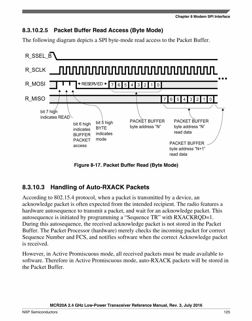
8.3.10.2.5 Packet Buffer Read Access (Byte Mode)
The following diagram depicts a SPI byte-mode read access to the Packet Buffer.
R_SSEL_B
R_SCLK
R_MOSI
bit 7 highindicates READ
R_MISO 7 6 5 4 3 2 1 0
PACKET BUFFERbyte address “N”
PACKET BUFFERbyte address “N”read data
PACKET BUFFERbyte address “N+1”read data
7 6 5 4 3 2 1 0RESERVED
bit 5 highBYTEindicatesmode
bit 6 highindicatesBUFFERPACKETaccess
Figure 8-17. Packet Buffer Read (Byte Mode)
8.3.10.3 Handling of Auto-RXACK Packets
According to 802.15.4 protocol, when a packet is transmitted by a device, anacknowledge packet is often expected from the intended recipient. The radio features ahardware autosequence to transmit a packet, and wait for an acknowledge packet. Thisautosequence is initiated by programming a “Sequence TR” with RXACKRQD=1.During this autosequence, the received acknowledge packet is not stored in the PacketBuffer. The Packet Processor (hardware) merely checks the incoming packet for correctSequence Number and FCS, and notifies software when the correct Acknowledge packetis received.
However, in Active Promiscuous mode, all received packets must be made available tosoftware. Therefore in Active Promiscuous mode, auto-RXACK packets will be stored inthe Packet Buffer.
Chapter 8 Modem SPI Interface
MCR20A 2.4 GHz Low-Power Transceiver Reference Manual, Rev. 3, July 2016
NXP Semiconductors 125
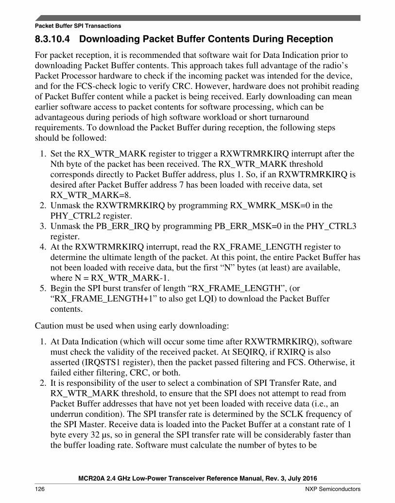
8.3.10.4 Downloading Packet Buffer Contents During Reception
For packet reception, it is recommended that software wait for Data Indication prior todownloading Packet Buffer contents. This approach takes full advantage of the radio’sPacket Processor hardware to check if the incoming packet was intended for the device,and for the FCS-check logic to verify CRC. However, hardware does not prohibit readingof Packet Buffer content while a packet is being received. Early downloading can meanearlier software access to packet contents for software processing, which can beadvantageous during periods of high software workload or short turnaroundrequirements. To download the Packet Buffer during reception, the following stepsshould be followed:
1. Set the RX_WTR_MARK register to trigger a RXWTRMRKIRQ interrupt after theNth byte of the packet has been received. The RX_WTR_MARK thresholdcorresponds directly to Packet Buffer address, plus 1. So, if an RXWTRMRKIRQ isdesired after Packet Buffer address 7 has been loaded with receive data, setRX_WTR_MARK=8.
2. Unmask the RXWTRMRKIRQ by programming RX_WMRK_MSK=0 in thePHY_CTRL2 register.
3. Unmask the PB_ERR_IRQ by programming PB_ERR_MSK=0 in the PHY_CTRL3register.
4. At the RXWTRMRKIRQ interrupt, read the RX_FRAME_LENGTH register todetermine the ultimate length of the packet. At this point, the entire Packet Buffer hasnot been loaded with receive data, but the first “N” bytes (at least) are available,where N = RX_WTR_MARK-1.
5. Begin the SPI burst transfer of length “RX_FRAME_LENGTH”, (or“RX_FRAME_LENGTH+1” to also get LQI) to download the Packet Buffercontents.
Caution must be used when using early downloading:
1. At Data Indication (which will occur some time after RXWTRMRKIRQ), softwaremust check the validity of the received packet. At SEQIRQ, if RXIRQ is alsoasserted (IRQSTS1 register), then the packet passed filtering and FCS. Otherwise, itfailed either filtering, CRC, or both.
2. It is responsibility of the user to select a combination of SPI Transfer Rate, andRX_WTR_MARK threshold, to ensure that the SPI does not attempt to read fromPacket Buffer addresses that have not yet been loaded with receive data (i.e., anunderrun condition). The SPI transfer rate is determined by the SCLK frequency ofthe SPI Master. Receive data is loaded into the Packet Buffer at a constant rate of 1byte every 32 µs, so in general the SPI transfer rate will be considerably faster thanthe buffer loading rate. Software must calculate the number of bytes to be
Packet Buffer SPI Transactions
MCR20A 2.4 GHz Low-Power Transceiver Reference Manual, Rev. 3, July 2016
126 NXP Semiconductors
downloaded (based on RX_FRAME_LENGTH), and then set the RX_WTR_MARKthreshold based on the ratio of SPI transfer rate to buffer loading rate.
If the steps above have not been followed correctly, and a Packet Buffer underrun occurs,this means the SPI read address of the Packet Buffer has overtaken the RX demodulatorwrite address. A PB_ERR_IRQ interrupt will be raised to indicate this condition. APB_ERR_IRQ is not catastrophic. The following steps should be taken to recover from aPB_ERR_IRQ:
1. Abort the SPI transfer in progress, and discard the data received so far, because theSPI transfer has been corrupted.
2. Clear the PB_ERR_IRQ by writing a ‘1’ to the PB_ERR_IRQ bit in the IRQSTS2register.
3. Restart the SPI transfer to download the Packet Buffer again. The design of thePacket Buffer ensures that read data has not been lost.
8.3.10.5 Registers Related to Packet Buffer Operation
PB_ERR_IRQ - Indicates that a Packet Buffer Underrun Error has occurred. Thiscondition can occur if a SPI burst read access to the Packet Buffer begins before theincoming packet is completely received, and the SPI PB read address overtakes the RXdemodulator write address. (See Downloading Packet Buffer Contents During Receptionfor information on how to avoid this condition, and what to do if it does occur). Softwaremust write a ‘1’ to this bit to clear the interrupt. The PB_ERR_IRQ interrupt can occuronly during SPI BURST accesses to Packet Buffer; SPI BYTE mode accesses to PacketBuffer will not trigger a PB_ERR_IRQ even if the SPI address is greater than the RXDemodulator address.
1: Packet Buffer Underrun Error has occurred since the last time this bit was cleared bysoftware
0: Packet Buffer Underrun Error has not occurred since the last time this bit was clearedby software
ACTIVE_PROMISCUOUS - Normally, received packets that are of Frame Type“Acknowledge”, received in response to a packet transmitted by the radio, are not storedin the Packet Buffer. Such packets are expected during a Sequence TR withRXACKRQD=1. In Active Promiscuous mode, software must have access to all receivepacket data, even “auto-RXACK” packets. This bit allows such packets to be stored inthe Packet Buffer.
1: Allow “auto-RXACK” packets to be stored in the Packet Buffer
0: Don’t allow “auto-RXACK” packets to be stored in the Packet Buffer (default)
Chapter 8 Modem SPI Interface
MCR20A 2.4 GHz Low-Power Transceiver Reference Manual, Rev. 3, July 2016
NXP Semiconductors 127

8.4 Configuring MCU for Proper SPI OperationThe MCU port control must be configured as follows to operate with the modem SPI:
• PTB10 should be configured as SPI1_PCS0• PTB11 should be configured as SPI1_SCK• PTB16 should be configured as SPI1_SOUT• PTB17 should be configured as SPI1_SIN. Also, the default configuration of the
modem R_MISO is that the modem tri-states this output when the R_SSEL_B is notasserted. The PTB17 pad should be configured with a pull-up or pull-down enabled.
The MCU DSPI module must also be configured for proper operation to meet the modemSPI transaction format. The following conditions must be met:
• MCU is master• Maximum baud rate is 9 MHz for reads, and 16 MHz for writes• Proper clock format must be selected, i.e., CPHA=0 and CPOL=0• SPI data must be transferred MSB first• The following modem SPI timings parameters must not be violated:
• tCSC (R_SSEL_B assertion to SCK delay) must be no less than 31.25ns• tASC (SCK to R_SSEL_B deassertion delay) must be no less than 31.25ns• tDT (R_SSEL_B deasserted idle time) must be no less than 62.5ns
The following sections describe the DSPI configuration in more detail. Refer to theMCU: Serial Peripheral Interface (SPI) chapter.
8.4.1 DSPI Mode Configuration
The following DSPI1 register settings are required to communicate correctly with themodem SPI:
• MSTR (SPI1_MCR, bit 31). MSTR =1 to configure the DSPI for master mode• PCSIS[0] (SPI1_MCR, bit 16). PCSIS[0]=1 must be set to indicate that the inactive
state of PCS0 is high• CPOL (SPI1_CTARn, bit 26) - CPOL=0 to select the correct clock polarity (active
high / inactive low)• CPHA (SPI1_CTARn, bit 25) - CPHA=0 to select the correct clock phase (data
captured on rising edge, changed on falling edge)• LSBFE (SPI1_CTARn, bit 24) - LSBFE=0 to transfer data MSB first
Configuring MCU for Proper SPI Operation
MCR20A 2.4 GHz Low-Power Transceiver Reference Manual, Rev. 3, July 2016
128 NXP Semiconductors
8.4.2 DSPI Baud Rate
The DSPI baud rate needs to be configured so that it is no more than 9MHz for modemSPI reads and 16MHz for modem SPI writes. The DSPI baud rate is determined by theMCU bus clock frequency, as well as by several programmable register bits in the DSPI.
• PBR (SPI1_CTARn, bits 17:16) - selects the baud rate prescaler value• BR (SPI1_CTARn, bits 3:0) - select the baud rate scaler• DBR (SPI1_CTARn, bit 31) - selects a double baud rate mode
As an example, assuming a 50MHz bus clock, PBR could be programmed for a divide-by-3 value, BR could be programmed for a divide-by-2 value, and DBR could beprogrammed to 0 to achieve an 8.3MHz SPI clock rate. For SPI writes, the PBR could bechanged to a divide-by-2 value to realize a 12.5MHz SPI clock rate.
If a 32MHz bus clock is used, PBR could be programmed for a divide-by-2 value, BRcould be programmed for a divide-by-2 value, and DBR could be programmed to 0 toachieve an 8MHz SPI clock rate. For SPI writes, the DBR could be changed to 1 torealize a 16MHz SPI clock rate.
Refer to the MCU: Serial Peripheral Interface (SPI) chapter for more information on baudrate.
8.4.3 DSPI Timing Control
The DSPI provides the following programmable control relating to the SPI timingparameters tCSC, tASC, and tDT:
• PCSSCK (SPI1_CTARn, bits 23:22) and CSSCK (SPI1_CTARn, bits 15:12) - thesecontrol the delay from PCS assertion to the first SCK edge, that is, tCSC
• PASC (SPI1_CTARn, bits 21:20) and ASC (SPI1_CTARn, bits 11:8) - these controlthe delay from the last SCK edge to the negation of PCS, that is, tASC
• PDT (SPI1_CTARn, bits 19:18) and DT (SPI1_CTARn, bits 7:4) - these control thedelay from the negation of PCS to the assertion of PCS for the next SPI frame, thatis, tDT
Since the maximum bus clock in the MCU is 50MHz, tCSC can be no more than 40nsregardless of programming. So PCSSCK and CSSCK can be programmed to their defaultvalues (device-by-1 and divide-by-2 respectively) to minimize this delay and still meetthe requirement that tCSC be no less than 32.5ns.
Chapter 8 Modem SPI Interface
MCR20A 2.4 GHz Low-Power Transceiver Reference Manual, Rev. 3, July 2016
NXP Semiconductors 129
Likewise, tASC can be no more than 40ns regardless of programming since the MCU busclock 50MHz limit. So PASC and ASC can also be programmed to their default values(device-by-1 and divide-by-2 respectively) to minimize this delay and still meet therequirement that tASC be no less than 32.5ns.
However, depending on the bus frequency, the PDT and DT may need to be programmedto ensure that tDT is no less than 62.5ns. If the bus clock is 32MHz or less, the defaultprogramming for PDT and DT can be used, since then tDTwill be no more than 62.5ns.However, with a 50MHz bus clock, the default programming for PDT and DT wouldcause tDT to be 40ns, which does not meet the modem requirement. Programming DT to adivide-by-4 value (instead of default divide-by-2) when the bus clock is 50MHz wouldincrease tDT to 80ns to meet the modem timing requirement.
Refer to the MCU: Serial Peripheral Interface (SPI) chapter for more information on baudrate and clock delay generation.
Configuring MCU for Proper SPI Operation
MCR20A 2.4 GHz Low-Power Transceiver Reference Manual, Rev. 3, July 2016
130 NXP Semiconductors
Chapter 9Modem: SPI Register Descriptions
9.1 IntroductionThis section provides a complete listing of all the modem registers, including registeraddress, access modes, descriptions, and references to other documents for morecomplete information.
The transceiver registers allow the MCU to communicate and control the radio as well asreceive feedback and status information. All radio registers are accessible via a SPIinterface only. No other means of accessing the transceiver registers is possible. Theregisters are divided into two categories; direct and indirect. The first 64 registers are“Direct Access”, meaning only a single SPI control word is required to identify theregister to be accessed. The remaining registers are “Indirect Access” and use a pointerregister followed by a data register as discussed following.
Indirect access registers use a pointer register and a window register for access in theindirect space. The pointer register (IAR_INDEX) and the data register (IAR_DATA)occupy the last two registers slots in Direct Space; addresses 0x3E and 0x3F respectively.Both direct- and indirect-access registers can be accessed in SPI burst mode, in which theSPI control word addresses the first register in the burst. After the first register in theburst is accessed, the hardware will auto-increment the register address so thatsubsequent sequential registers can be accessed during a single multi-byte SPItransaction. The length of the burst is not limited by hardware.
Direct access burst mode is available in all power states, including HIBERNATE.Indirect access burst mode is restricted to states during which the crystal oscillator isrunning (e.g., DOZE, IDLE, RUN); this excludes HIBERNATE state. Indirect registeraccess in HIBERNATE state is restricted to single-byte.
A few registers, which control special functions within the IC, should not be accessed inHIBERNATE state; these are identified in the “Register Description” tables later in thisdocument. However, most registers are 100% accessible in all power states, includingHIBERNATE.
MCR20A 2.4 GHz Low-Power Transceiver Reference Manual, Rev. 3, July 2016
NXP Semiconductors 131
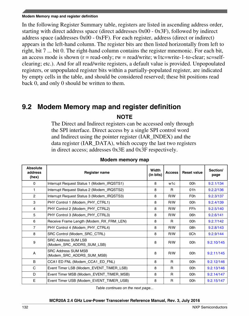
In the following Register Summary table, registers are listed in ascending address order,starting with direct address space (direct addresses 0x00 - 0x3F), followed by indirectaddress space (addresses 0x00 - 0xFF). For each register, address (direct or indirect)appears in the left-hand column. The register bits are then listed horizontally from left toright, bit 7 ... bit 0. The right-hand column contains the register mnemonic. For each bit,an access mode is shown (r = read-only; rw = read/write; w1tc=write-1-to-clear; sc=self-clearing; etc.). And for all read/write registers, a default value is provided. Unpopoulatedregisters, or unpopulated register bits within a partially-populated register, are indicatedby empty cells in the table, and should be considered reserved; these bit positions readback 0, and only 0 should be written to them.
9.2 Modem Memory map and register definitionNOTE
The Direct and Indirect registers can be accessed only throughthe SPI interface. Direct access by a single SPI control wordand Indirect using the pointer register (IAR_INDEX) and thedata register (IAR_DATA), which occupy the last two registersin direct access; addresses 0x3E and 0x3F respectively.
Modem memory map
Absoluteaddress
(hex)Register name
Width(in bits)
Access Reset valueSection/
page
0 Interrupt Request Status 1 (Modem_IRQSTS1) 8 w1c 00h 9.2.1/134
1 Interrupt Request Status 2 (Modem_IRQSTS2) 8 R 01h 9.2.2/136
2 Interrupt Request Status 3 (Modem_IRQSTS3) 8 R/W F0h 9.2.3/137
3 PHY Control 1 (Modem_PHY_CTRL1) 8 R/W 00h 9.2.4/139
4 PHY Control 2 (Modem_PHY_CTRL2) 8 R/W FFh 9.2.5/140
5 PHY Control 3 (Modem_PHY_CTRL3) 8 R/W 06h 9.2.6/141
6 Receive Frame Length (Modem_RX_FRM_LEN) 8 R 00h 9.2.7/142
7 PHY Control 4 (Modem_PHY_CTRL4) 8 R/W 08h 9.2.8/143
8 SRC Control (Modem_SRC_CTRL) 8 R/W 0Ch 9.2.9/144
9SRC Address SUM LSB(Modem_SRC_ADDRS_SUM_LSB)
8 R/W 00h 9.2.10/145
ASRC Address SUM MSB(Modem_SRC_ADDRS_SUM_MSB)
8 R/W 00h 9.2.11/145
B CCA1 ED FNL (Modem_CCA1_ED_FNL) 8 R 00h 9.2.12/146
C Event Timer LSB (Modem_EVENT_TIMER_LSB) 8 R 00h 9.2.13/146
D Event Timer MSB (Modem_EVENT_TIMER_MSB) 8 R 00h 9.2.14/147
E Event Timer USB (Modem_EVENT_TIMER_USB) 8 R 00h 9.2.15/147
Table continues on the next page...
Modem Memory map and register definition
MCR20A 2.4 GHz Low-Power Transceiver Reference Manual, Rev. 3, July 2016
132 NXP Semiconductors
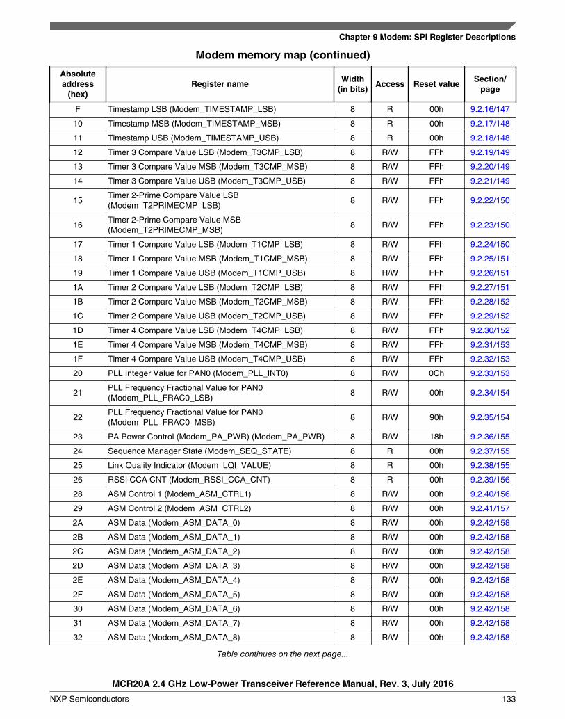
Modem memory map (continued)
Absoluteaddress
(hex)Register name
Width(in bits)
Access Reset valueSection/
page
F Timestamp LSB (Modem_TIMESTAMP_LSB) 8 R 00h 9.2.16/147
10 Timestamp MSB (Modem_TIMESTAMP_MSB) 8 R 00h 9.2.17/148
11 Timestamp USB (Modem_TIMESTAMP_USB) 8 R 00h 9.2.18/148
12 Timer 3 Compare Value LSB (Modem_T3CMP_LSB) 8 R/W FFh 9.2.19/149
13 Timer 3 Compare Value MSB (Modem_T3CMP_MSB) 8 R/W FFh 9.2.20/149
14 Timer 3 Compare Value USB (Modem_T3CMP_USB) 8 R/W FFh 9.2.21/149
15Timer 2-Prime Compare Value LSB(Modem_T2PRIMECMP_LSB)
8 R/W FFh 9.2.22/150
16Timer 2-Prime Compare Value MSB(Modem_T2PRIMECMP_MSB)
8 R/W FFh 9.2.23/150
17 Timer 1 Compare Value LSB (Modem_T1CMP_LSB) 8 R/W FFh 9.2.24/150
18 Timer 1 Compare Value MSB (Modem_T1CMP_MSB) 8 R/W FFh 9.2.25/151
19 Timer 1 Compare Value USB (Modem_T1CMP_USB) 8 R/W FFh 9.2.26/151
1A Timer 2 Compare Value LSB (Modem_T2CMP_LSB) 8 R/W FFh 9.2.27/151
1B Timer 2 Compare Value MSB (Modem_T2CMP_MSB) 8 R/W FFh 9.2.28/152
1C Timer 2 Compare Value USB (Modem_T2CMP_USB) 8 R/W FFh 9.2.29/152
1D Timer 4 Compare Value LSB (Modem_T4CMP_LSB) 8 R/W FFh 9.2.30/152
1E Timer 4 Compare Value MSB (Modem_T4CMP_MSB) 8 R/W FFh 9.2.31/153
1F Timer 4 Compare Value USB (Modem_T4CMP_USB) 8 R/W FFh 9.2.32/153
20 PLL Integer Value for PAN0 (Modem_PLL_INT0) 8 R/W 0Ch 9.2.33/153
21PLL Frequency Fractional Value for PAN0(Modem_PLL_FRAC0_LSB)
8 R/W 00h 9.2.34/154
22PLL Frequency Fractional Value for PAN0(Modem_PLL_FRAC0_MSB)
8 R/W 90h 9.2.35/154
23 PA Power Control (Modem_PA_PWR) (Modem_PA_PWR) 8 R/W 18h 9.2.36/155
24 Sequence Manager State (Modem_SEQ_STATE) 8 R 00h 9.2.37/155
25 Link Quality Indicator (Modem_LQI_VALUE) 8 R 00h 9.2.38/155
26 RSSI CCA CNT (Modem_RSSI_CCA_CNT) 8 R 00h 9.2.39/156
28 ASM Control 1 (Modem_ASM_CTRL1) 8 R/W 00h 9.2.40/156
29 ASM Control 2 (Modem_ASM_CTRL2) 8 R/W 00h 9.2.41/157
2A ASM Data (Modem_ASM_DATA_0) 8 R/W 00h 9.2.42/158
2B ASM Data (Modem_ASM_DATA_1) 8 R/W 00h 9.2.42/158
2C ASM Data (Modem_ASM_DATA_2) 8 R/W 00h 9.2.42/158
2D ASM Data (Modem_ASM_DATA_3) 8 R/W 00h 9.2.42/158
2E ASM Data (Modem_ASM_DATA_4) 8 R/W 00h 9.2.42/158
2F ASM Data (Modem_ASM_DATA_5) 8 R/W 00h 9.2.42/158
30 ASM Data (Modem_ASM_DATA_6) 8 R/W 00h 9.2.42/158
31 ASM Data (Modem_ASM_DATA_7) 8 R/W 00h 9.2.42/158
32 ASM Data (Modem_ASM_DATA_8) 8 R/W 00h 9.2.42/158
Table continues on the next page...
Chapter 9 Modem: SPI Register Descriptions
MCR20A 2.4 GHz Low-Power Transceiver Reference Manual, Rev. 3, July 2016
NXP Semiconductors 133
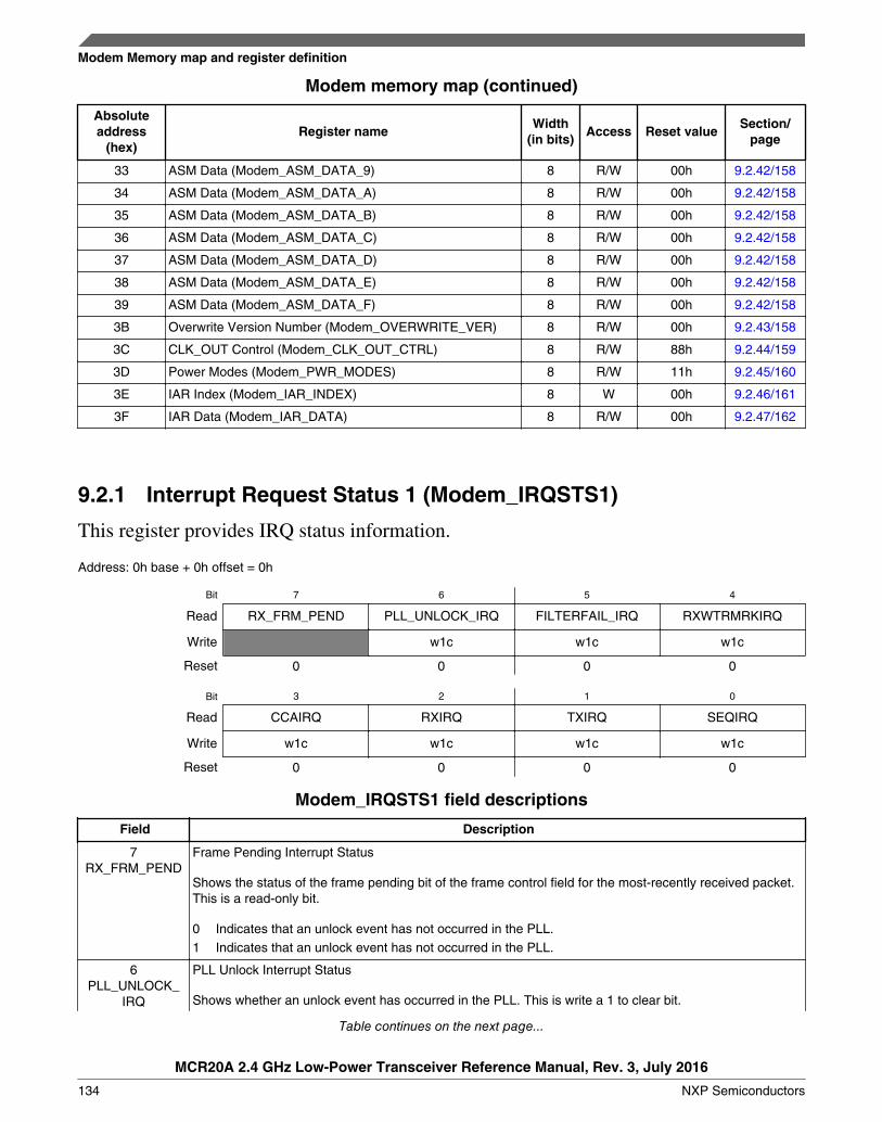
Modem memory map (continued)
Absoluteaddress
(hex)Register name
Width(in bits)
Access Reset valueSection/
page
33 ASM Data (Modem_ASM_DATA_9) 8 R/W 00h 9.2.42/158
34 ASM Data (Modem_ASM_DATA_A) 8 R/W 00h 9.2.42/158
35 ASM Data (Modem_ASM_DATA_B) 8 R/W 00h 9.2.42/158
36 ASM Data (Modem_ASM_DATA_C) 8 R/W 00h 9.2.42/158
37 ASM Data (Modem_ASM_DATA_D) 8 R/W 00h 9.2.42/158
38 ASM Data (Modem_ASM_DATA_E) 8 R/W 00h 9.2.42/158
39 ASM Data (Modem_ASM_DATA_F) 8 R/W 00h 9.2.42/158
3B Overwrite Version Number (Modem_OVERWRITE_VER) 8 R/W 00h 9.2.43/158
3C CLK_OUT Control (Modem_CLK_OUT_CTRL) 8 R/W 88h 9.2.44/159
3D Power Modes (Modem_PWR_MODES) 8 R/W 11h 9.2.45/160
3E IAR Index (Modem_IAR_INDEX) 8 W 00h 9.2.46/161
3F IAR Data (Modem_IAR_DATA) 8 R/W 00h 9.2.47/162
9.2.1 Interrupt Request Status 1 (Modem_IRQSTS1)
This register provides IRQ status information.
Address: 0h base + 0h offset = 0h
Bit 7 6 5 4
Read RX_FRM_PEND PLL_UNLOCK_IRQ FILTERFAIL_IRQ RXWTRMRKIRQ
Write w1c w1c w1c
Reset 0 0 0 0
Bit 3 2 1 0
Read CCAIRQ RXIRQ TXIRQ SEQIRQ
Write w1c w1c w1c w1c
Reset 0 0 0 0
Modem_IRQSTS1 field descriptions
Field Description
7RX_FRM_PEND
Frame Pending Interrupt Status
Shows the status of the frame pending bit of the frame control field for the most-recently received packet.This is a read-only bit.
0 Indicates that an unlock event has not occurred in the PLL.1 Indicates that an unlock event has not occurred in the PLL.
6PLL_UNLOCK_
IRQ
PLL Unlock Interrupt Status
Shows whether an unlock event has occurred in the PLL. This is write a 1 to clear bit.
Table continues on the next page...
Modem Memory map and register definition
MCR20A 2.4 GHz Low-Power Transceiver Reference Manual, Rev. 3, July 2016
134 NXP Semiconductors
Modem_IRQSTS1 field descriptions (continued)
Field Description
0 Indicates that an unlock event has not occurred in the PLL.1 Indicates that an unlock event has not occurred in the PLL.
5FILTERFAIL_IRQ
Receiver Packet Filter Fail Interrupt Status
Shows whether the most-recently received packet has been rejected due to elements within the packet.This is write a 1 to clear bit.
• If PAN0 and PAN1 occupy different channels and CURRENT_NETWORK=0, FILTERFAIL_IRQapplies to PAN0.
• If PAN0 and PAN1 occupy different channels and CURRENT_NETWORK=1, FILTERFAIL_IRQapplies to PAN1.
• If PAN0 and PAN1 occupy the same channel, FILTERFAIL_IRQ is the logical ‘AND’ of the individualPANs’ Filter Fail status.
4RXWTRMRKIRQ
Receiver Byte Count Water Mark Interrupt Status
Shows whether the number of bytes specified in the RX_WTR_MARK register has been reached. This iswrite a 1 to clear bit.
0 Indicates that the number of bytes specified in the RX_WTR_MARK register has not been reached1 Indicates that the number of bytes specified in the RX_WTR_MARK register has been reached
3CCAIRQ
Clear Channel Assessment Interrupt Status
Shows the status of a CCA operation. This is write a 1 to clear bit. See the sequence manager section fora description of the timing of this interrupt.
0 Indicates that the completion of a CCA operation has not occurred.1 Indicates that the completion of a CCA operation has occurred.
2RXIRQ
Receiver Interrupt Status
Shows the status of a receive operation. This is write a 1 to clear bit.
0 Indicates that the completion of a receive operation has not occurred.1 Indicates that the completion of a receive operation has occurred.
1TXIRQ
Transmitter Interrupt Status
Shows the status of a transmit operation. This is write a 1 to clear bit.
0 Indicates that the completion of a transmit operation has not occurred.1 Indicates that the completion of a transmit operation has occurred.
0SEQIRQ
Sequence-end Interrupt Request Status
This interrupt will assert whenever the Sequence Manager transitions from non-idle to idle state, for anyreason. This is write a 1 to clear bit.
0 Indicates that the completion of an autosequence has not occurred.1 Indicates that the completion of an autosequence has occurred.
Chapter 9 Modem: SPI Register Descriptions
MCR20A 2.4 GHz Low-Power Transceiver Reference Manual, Rev. 3, July 2016
NXP Semiconductors 135
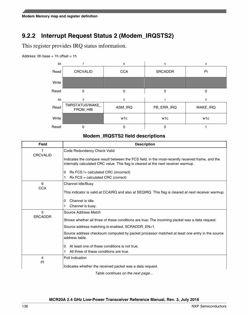
9.2.2 Interrupt Request Status 2 (Modem_IRQSTS2)
This register provides IRQ status information.
Address: 0h base + 1h offset = 1h
Bit 7 6 5 4
Read CRCVALID CCA SRCADDR PI
Write
Reset 0 0 0 0
Bit 3 2 1 0
ReadTMRSTATUS/WAKE_
FROM_HIBASM_IRQ PB_ERR_IRQ WAKE_IRQ
Write w1c w1c w1c
Reset 0 0 0 1
Modem_IRQSTS2 field descriptions
Field Description
7CRCVALID
Code Redundancy Check Valid
Indicates the compare result between the FCS field, in the most-recently received frame, and theinternally calculated CRC value. This flag is cleared at the next receiver warmup.
0 Rx FCS != calculated CRC (incorrect)1 Rx FCS = calculated CRC (correct)
6CCA
Channel Idle/Busy
This indicator is valid at CCAIRQ and also at SEQIRQ. This flag is cleared at next receiver warmup.
0 Channel is idle.1 Channel is busy.
5SRCADDR
Source Address Match
Shows whether all three of these conditions are true: The incoming packet was a data request.
Source address matching is enabled, SCRADDR_EN=1.
Source address checksum computed by packet processor matched at least one entry in the sourceaddress table.
0 At least one of these conditions is not true.1 All three of these conditions are true.
4PI
Poll Indication
Indicates whether the received packet was a data request.
Table continues on the next page...
Modem Memory map and register definition
MCR20A 2.4 GHz Low-Power Transceiver Reference Manual, Rev. 3, July 2016
136 NXP Semiconductors
Modem_IRQSTS2 field descriptions (continued)
Field Description
0 Indicates that the received packet was not a data request.1 Indicates that the received packet was a data request, regardless of whether a source address
table match occurred, or whether source address matching is enabled. (See SRCADDR_EN indirect register 0x08, MODEM_SRC_CTRL.)
3TMRSTATUS/WAKE_
FROM_HIB
Timer Status/Wake from Hibernate
This is a dual-purpose, read-only status bit. Its value is dependent on the WAKE_IRQ bit. Used toindicate either wakeup status or timer status.
0 If WAKE_IRQ=1, a 0 indicates that a wakeup from POR has occurred.
If WAKE_IRQ=0, a 0 indicates that no TMRxIRQ is asserted. See the IRQST3 register for theindividual timer interrupt status bits.
1 If WAKE_IRQ=1, a 1 indicates that a wakeup from Hibernate has occurred.
If WAKE_IRQ=0, a 1 indicates that at least one of the TMRxIRQ is asserted. See the IRQST3register for the individual timer interrupt status bits.
2ASM_IRQ
AES Interrupt Flag
A 1 indicates the completion of a AES operation completed. This is write a 1 to clear bit.
1PB_ERR_IRQ
Packet Buffer Underrun Error Interrupt Status
Shows whether a packet buffer underrun error has occurred since the last time this bit was clearedby software. This is a write 1 to clear bit. PB_ERR_IRQ will occur only when the SPI packet bufferaccess is Burst mode (not Byte mode).
0 A packet buffer underrun error has not occurred since the last time this bit was cleared bysoftware.
1 A packet buffer underrun error has occurred since the last time this bit was cleared by software.
0WAKE_IRQ
Wake Interrupt Status
Indicates that either a wake-from-POR or a wake-from-Hibernate event has occured. This is write a1 to clear bit.
0 Indicates that neither wake event has occurred.1 Indicates that one of these wake events has occurred. See the WAKE_FROM_HIB/
TMRSTATUS bit to see which type of wake has occurred.
9.2.3 Interrupt Request Status 3 (Modem_IRQSTS3)
This register provides IRQ status information.
Address: 0h base + 2h offset = 2h
Bit 7 6 5 4 3 2 1 0
ReadTMR4MSK TMR3MSK TMR2MSK TMR1MSK
TMR4IRQ TMR3IRQ TMR2IRQ TMR1IRQ
Write w1c w1c w1c w1c
Reset 1 1 1 1 0 0 0 0
Chapter 9 Modem: SPI Register Descriptions
MCR20A 2.4 GHz Low-Power Transceiver Reference Manual, Rev. 3, July 2016
NXP Semiconductors 137
Modem_IRQSTS3 field descriptions
Field Description
7TMR4MSK
Timer Comparator 4 Interrupt Mask
0 Allows interrupt when comparator matches event timer count.1 Disables interrupt generation, but allows a TMR4IRQ flag to be set.
6TMR3MSK
Timer Comparator 3 Interrupt Mask
0 Allows interrupt when comparator matches event timer count.1 Disables interrupt generation, but allows a TMR3IRQ flag to be set.
5TMR2MSK
Timer Comparator 2 Interrupt Mask
0 Allows interrupt when comparator matches event timer count.1 Disables interrupt generation, but allows a TMR2IRQ flag to be set.
4TMR1MSK
Timer Comparator 1 Interrupt Mask
0 Allows interrupt when comparator matches event timer count.1 Disables interrupt generation, but allows a TMR1IRQ flag to be set.
3TMR4IRQ
Timer Comparator 4 Interrupt Status
Indicates whether the T4CMP comparator value matched the event timer counter. This is a write 1 to clearbit.
0 Indicates that the T4CMP comparator value does not match the event timer counter.1 Indicates that the T4CMP comparator value does match the event timer counter.
2TMR3IRQ
Timer Comparator 3 Interrupt Status
Indicates whether the T1CMP comparator value matched the event timer counter. This is a write 1 to clearbit.
0 Indicates that the T3CMP comparator value does not match the event timer counter.1 Indicates that the T3CMP comparator value does match the event timer counter.
1TMR2IRQ
Timer Comparator 2 Interrupt Status
Indicates whether the T2CMP comparator value matched the event timer counter. This is a write 1 to clearbit.
0 Indicates that the T2CMP comparator value does not match the event timer counter.1 Indicates that the T2CMP comparator value does match the event timer counter.
0TMR1IRQ
Timer Comparator 1 Interrupt Status
Indicates whether the T1CMP comparator value matched the event timer counter. This is a write 1 to clearbit.
0 Indicates that the T1CMP comparator value does not match the event timer counter.1 Indicates that the T1CMP comparator value does match the event timer counter.
Modem Memory map and register definition
MCR20A 2.4 GHz Low-Power Transceiver Reference Manual, Rev. 3, July 2016
138 NXP Semiconductors
9.2.4 PHY Control 1 (Modem_PHY_CTRL1)
This register is used to control the PHY.
Address: 0h base + 3h offset = 3h
Bit 7 6 5 4 3 2 1 0
Read TMRTRIGEN
SLOTTED CCABFRTX RXACKRQD AUTOACK XCVSEQWrite
Reset 0 0 0 0 0 0 0 0
Modem_PHY_CTRL1 field descriptions
Field Description
7TMRTRIGEN
Timer 2 Trigger Enable
This control bit allows the transceivers programmed sequence to be immediate or delayed by T2CMP orT2PRIMECMP count.
0 Programmed sequence initiates immediately upon write to XCVSEQ.1 Allow timer TC2 (or TC2’) to initiate a preprogrammed sequence (see XCVSEQ register).
6SLOTTED
Slotted Mode
For beacon-enabled networks. Applies only to Sequences T, TR, and R, ignored during all othersequences. Used, in concert with CCABFRTX, to determine how many CCA measurements are requiredprior to a transmit operation. Also used during R sequence to determine whether the ensuing transmitacknowledge frame (if any) needs to be synchronized to a backoff slot boundary.
0 Non-slotted1 Slotted
5CCABFRTX
CCA Before TX
Applies only to sequences T and TR. Ignored during all other sequences.
0 No CCA required. Transmit operation begins immediately.1 At least one CCA measurement is required prior to the transmit operation (see also SLOTTED).
4RXACKRQD
Receive Acknowledge Frame Required
Applies only to Sequence TR, ignored during all other sequences.
0 An ordinary receive frame (any type of frame) follows the transmit frame.1 A receive acknowledge frame is expected to follow the transmit frame (non-acknowledge frames are
rejected).
3AUTOACK
Auto Acklowledge Enable
Applies only to sequence R and sequence TR. Ignored during other sequences.
0 The sequence manager will not follow a receive frame with a Tx Ack frame, under any condition. Theautosequence will terminate after the receive frame.
1 The sequence manager will follow a receive frame with an automatic hardware-generated Tx Ackframe, assuming other necessary conditions are met.
XCVSEQ Transceiver Sequence Selector
Table continues on the next page...
Chapter 9 Modem: SPI Register Descriptions
MCR20A 2.4 GHz Low-Power Transceiver Reference Manual, Rev. 3, July 2016
NXP Semiconductors 139
Modem_PHY_CTRL1 field descriptions (continued)
Field Description
Selects an autosequence for the sequence manager to execute. Sequence initiation can be immediate, orscheduled (see TMRTRIGEN). A write of XCVSEQ=IDLE will abort any ongoing sequence. A write ofXCVSEQ=IDLE must always be performed after a sequence is complete, and before a new sequence isprogrammed. Any write to XCVSEQ other than XCVSEQ=IDLE during an ongoing sequence, shall beignored. The mapping of XCVSEQ to sequence types is as follows:
000 Idle (sequence I)001 Receive (sequence R)010 Transmit (sequence T)011 CCA (sequence C)100 Transmit/Receive (sequence TR)101 Continuous CCA (sequence CCCA)110 Reserved111 Reserved
9.2.5 PHY Control 2 (Modem_PHY_CTRL2)
This register is used to control the PHY.
Address: 0h base + 4h offset = 4h
Bit 7 6 5 4 3 2 1 0
Read
CRC_MSKPLL_
UNLOCK_MSK
FILTERFAIL_MSK
RX_WMRK_MSK
CCAMSK RXMSK TXMSK SEQMSKWrite
Reset 1 1 1 1 1 1 1 1
Modem_PHY_CTRL2 field descriptions
Field Description
7CRC_MSK
CRC Mask
0 The sequence manager ignores CRCVALID and considers the receive operation complete after thelast octet of the frame has been received.
1 The sequence manager requires CRCVALID=1 at the end of the received frame in order for thereceive operation to complete successfully; if CRCVALID=0, sequence manager will return topreamble-detect mode after the last octet of the frame has been received.
6PLL_UNLOCK_
MSK
PLL Unlock Mask
0 Allows PLL unlock event to generate an interrupt on IRQ_B.1 A PLL unlock event will set the PLL_UNLOCK_IRQ status bit, but an interrupt is not generated on
IRQ_B.
5FILTERFAIL_
MSK
Filter Fail Mask
0 Allows packet processor filtering Failure to generate an interrupt on IRQ_B.1 A packet processor filtering failure will set the FILTERFAIL_IRQ status bit, but an interrupt is not
generated on IRQ_B.
Table continues on the next page...
Modem Memory map and register definition
MCR20A 2.4 GHz Low-Power Transceiver Reference Manual, Rev. 3, July 2016
140 NXP Semiconductors
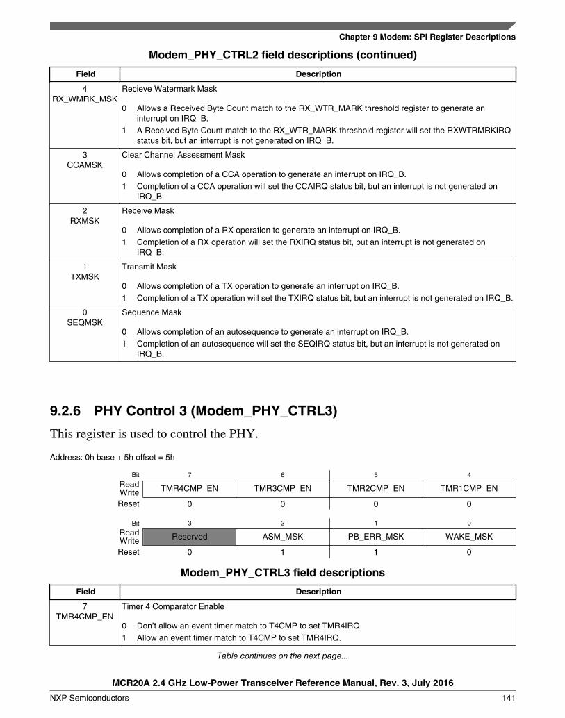
Modem_PHY_CTRL2 field descriptions (continued)
Field Description
4RX_WMRK_MSK
Recieve Watermark Mask
0 Allows a Received Byte Count match to the RX_WTR_MARK threshold register to generate aninterrupt on IRQ_B.
1 A Received Byte Count match to the RX_WTR_MARK threshold register will set the RXWTRMRKIRQstatus bit, but an interrupt is not generated on IRQ_B.
3CCAMSK
Clear Channel Assessment Mask
0 Allows completion of a CCA operation to generate an interrupt on IRQ_B.1 Completion of a CCA operation will set the CCAIRQ status bit, but an interrupt is not generated on
IRQ_B.
2RXMSK
Receive Mask
0 Allows completion of a RX operation to generate an interrupt on IRQ_B.1 Completion of a RX operation will set the RXIRQ status bit, but an interrupt is not generated on
IRQ_B.
1TXMSK
Transmit Mask
0 Allows completion of a TX operation to generate an interrupt on IRQ_B.1 Completion of a TX operation will set the TXIRQ status bit, but an interrupt is not generated on IRQ_B.
0SEQMSK
Sequence Mask
0 Allows completion of an autosequence to generate an interrupt on IRQ_B.1 Completion of an autosequence will set the SEQIRQ status bit, but an interrupt is not generated on
IRQ_B.
9.2.6 PHY Control 3 (Modem_PHY_CTRL3)
This register is used to control the PHY.
Address: 0h base + 5h offset = 5h
Bit 7 6 5 4
Read TMR4CMP_EN TMR3CMP_EN TMR2CMP_EN TMR1CMP_ENWriteReset 0 0 0 0
Bit 3 2 1 0
Read Reserved ASM_MSK PB_ERR_MSK WAKE_MSKWriteReset 0 1 1 0
Modem_PHY_CTRL3 field descriptions
Field Description
7TMR4CMP_EN
Timer 4 Comparator Enable
0 Don’t allow an event timer match to T4CMP to set TMR4IRQ.1 Allow an event timer match to T4CMP to set TMR4IRQ.
Table continues on the next page...
Chapter 9 Modem: SPI Register Descriptions
MCR20A 2.4 GHz Low-Power Transceiver Reference Manual, Rev. 3, July 2016
NXP Semiconductors 141
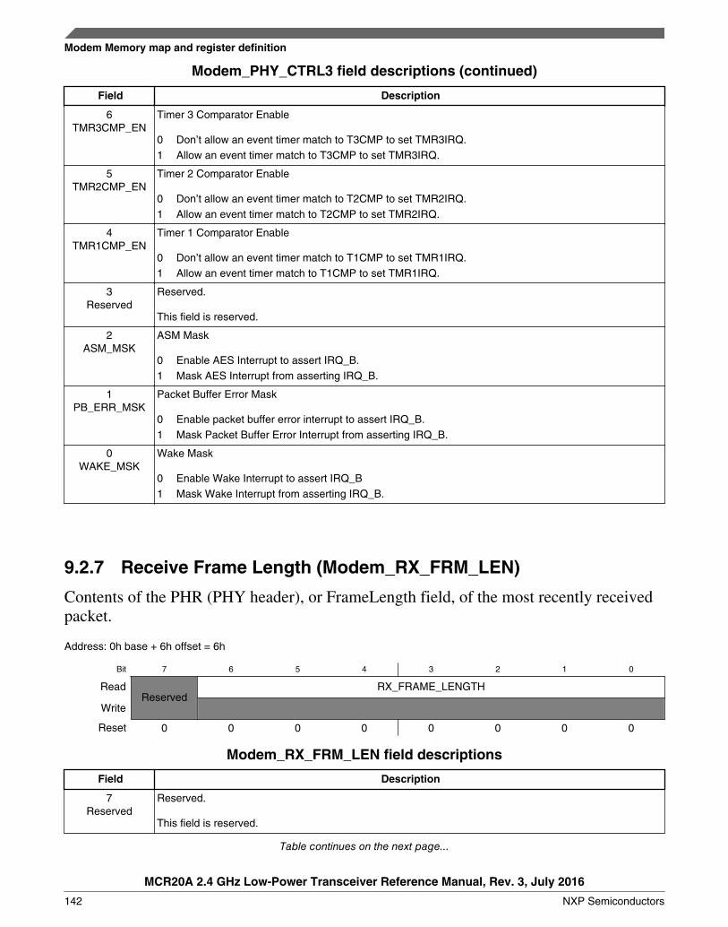
Modem_PHY_CTRL3 field descriptions (continued)
Field Description
6TMR3CMP_EN
Timer 3 Comparator Enable
0 Don’t allow an event timer match to T3CMP to set TMR3IRQ.1 Allow an event timer match to T3CMP to set TMR3IRQ.
5TMR2CMP_EN
Timer 2 Comparator Enable
0 Don’t allow an event timer match to T2CMP to set TMR2IRQ.1 Allow an event timer match to T2CMP to set TMR2IRQ.
4TMR1CMP_EN
Timer 1 Comparator Enable
0 Don’t allow an event timer match to T1CMP to set TMR1IRQ.1 Allow an event timer match to T1CMP to set TMR1IRQ.
3Reserved
Reserved.
This field is reserved.
2ASM_MSK
ASM Mask
0 Enable AES Interrupt to assert IRQ_B.1 Mask AES Interrupt from asserting IRQ_B.
1PB_ERR_MSK
Packet Buffer Error Mask
0 Enable packet buffer error interrupt to assert IRQ_B.1 Mask Packet Buffer Error Interrupt from asserting IRQ_B.
0WAKE_MSK
Wake Mask
0 Enable Wake Interrupt to assert IRQ_B1 Mask Wake Interrupt from asserting IRQ_B.
9.2.7 Receive Frame Length (Modem_RX_FRM_LEN)
Contents of the PHR (PHY header), or FrameLength field, of the most recently receivedpacket.
Address: 0h base + 6h offset = 6h
Bit 7 6 5 4 3 2 1 0
ReadReserved
RX_FRAME_LENGTH
Write
Reset 0 0 0 0 0 0 0 0
Modem_RX_FRM_LEN field descriptions
Field Description
7Reserved
Reserved.
This field is reserved.
Table continues on the next page...
Modem Memory map and register definition
MCR20A 2.4 GHz Low-Power Transceiver Reference Manual, Rev. 3, July 2016
142 NXP Semiconductors
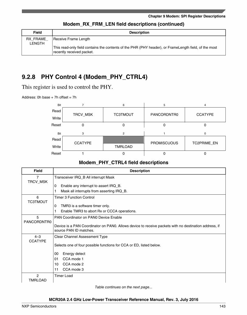
Modem_RX_FRM_LEN field descriptions (continued)
Field Description
RX_FRAME_LENGTH
Receive Frame Length
This read-only field contains the contents of the PHR (PHY header), or FrameLength field, of the mostrecently received packet.
9.2.8 PHY Control 4 (Modem_PHY_CTRL4)
This register is used to control the PHY.
Address: 0h base + 7h offset = 7h
Bit 7 6 5 4
ReadTRCV_MSK TC3TMOUT PANCORDNTR0 CCATYPE
Write
Reset 0 0 0 0
Bit 3 2 1 0
ReadCCATYPE PROMISCUOUS TC2PRIME_EN
Write TMRLOAD
Reset 1 0 0 0
Modem_PHY_CTRL4 field descriptions
Field Description
7TRCV_MSK
Transceiver IRQ_B All interrupt Mask
0 Enable any interrupt to assert IRQ_B.1 Mask all interrupts from asserting IRQ_B.
6TC3TMOUT
Timer 3 Function Control
0 TMR3 is a software timer only.1 Enable TMR3 to abort Rx or CCCA operations.
5PANCORDNTR0
PAN Coordinator on PAN0 Device Enable
Device is a PAN Coordinator on PAN0. Allows device to receive packets with no destination address, ifsource PAN ID matches.
4–3CCATYPE
Clear Channel Assessment Type
Selects one of four possible functions for CCA or ED, listed below.
00 Energy detect01 CCA mode 110 CCA mode 211 CCA mode 3
2TMRLOAD
Timer Load
Table continues on the next page...
Chapter 9 Modem: SPI Register Descriptions
MCR20A 2.4 GHz Low-Power Transceiver Reference Manual, Rev. 3, July 2016
NXP Semiconductors 143
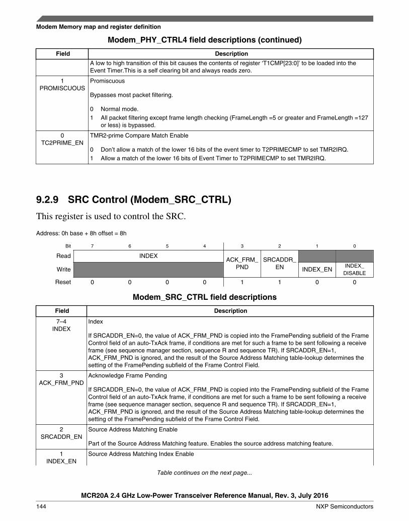
Modem_PHY_CTRL4 field descriptions (continued)
Field Description
A low to high transition of this bit causes the contents of register ‘T1CMP[23:0]’ to be loaded into theEvent Timer.This is a self clearing bit and always reads zero.
1PROMISCUOUS
Promiscuous
Bypasses most packet filtering.
0 Normal mode.1 All packet filtering except frame length checking (FrameLength =5 or greater and FrameLength =127
or less) is bypassed.
0TC2PRIME_EN
TMR2-prime Compare Match Enable
0 Don’t allow a match of the lower 16 bits of the event timer to T2PRIMECMP to set TMR2IRQ.1 Allow a match of the lower 16 bits of Event Timer to T2PRIMECMP to set TMR2IRQ.
9.2.9 SRC Control (Modem_SRC_CTRL)
This register is used to control the SRC.
Address: 0h base + 8h offset = 8h
Bit 7 6 5 4 3 2 1 0
Read INDEXACK_FRM_
PNDSRCADDR_
ENWrite INDEX_ENINDEX_
DISABLE
Reset 0 0 0 0 1 1 0 0
Modem_SRC_CTRL field descriptions
Field Description
7–4INDEX
Index
If SRCADDR_EN=0, the value of ACK_FRM_PND is copied into the FramePending subfield of the FrameControl field of an auto-TxAck frame, if conditions are met for such a frame to be sent following a receiveframe (see sequence manager section, sequence R and sequence TR). If SRCADDR_EN=1,ACK_FRM_PND is ignored, and the result of the Source Address Matching table-lookup determines thesetting of the FramePending subfield of the Frame Control Field.
3ACK_FRM_PND
Acknowledge Frame Pending
If SRCADDR_EN=0, the value of ACK_FRM_PND is copied into the FramePending subfield of the FrameControl field of an auto-TxAck frame, if conditions are met for such a frame to be sent following a receiveframe (see sequence manager section, sequence R and sequence TR). If SRCADDR_EN=1,ACK_FRM_PND is ignored, and the result of the Source Address Matching table-lookup determines thesetting of the FramePending subfield of the Frame Control Field.
2SRCADDR_EN
Source Address Matching Enable
Part of the Source Address Matching feature. Enables the source address matching feature.
1INDEX_EN
Source Address Matching Index Enable
Table continues on the next page...
Modem Memory map and register definition
MCR20A 2.4 GHz Low-Power Transceiver Reference Manual, Rev. 3, July 2016
144 NXP Semiconductors
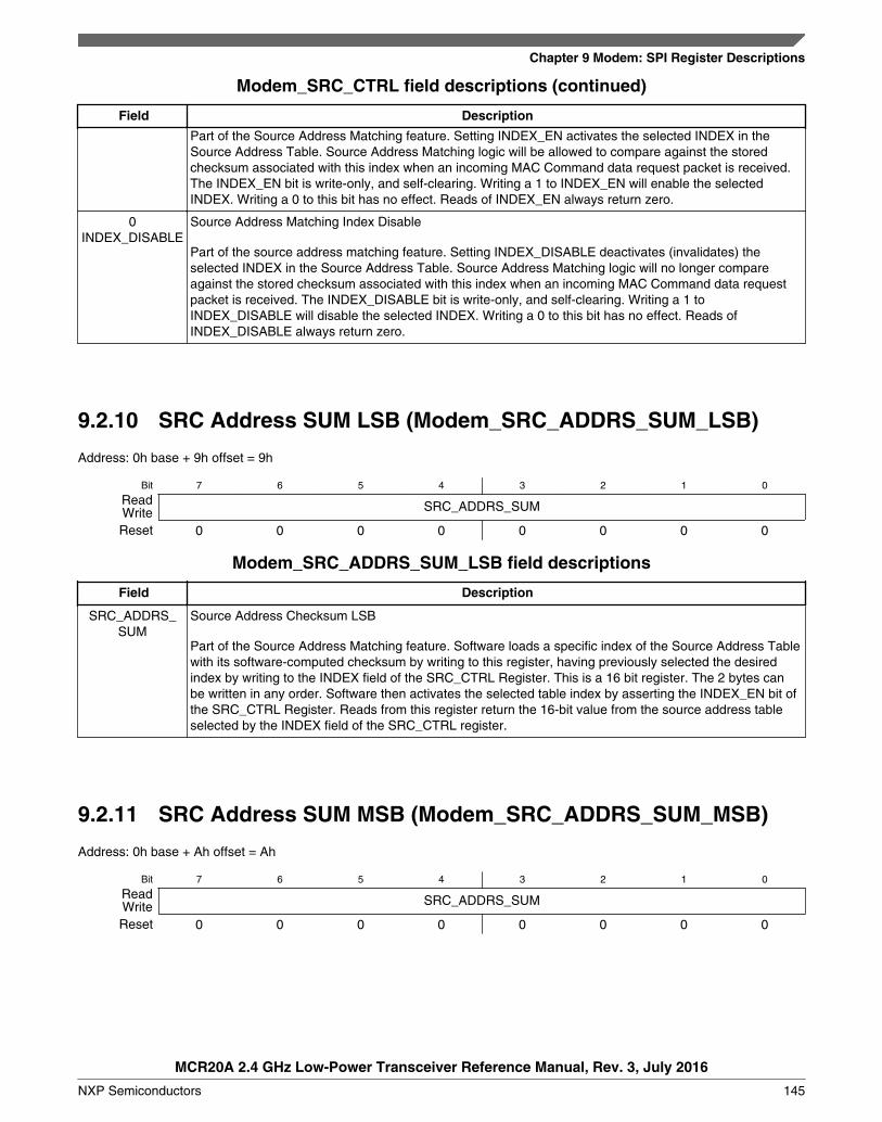
Modem_SRC_CTRL field descriptions (continued)
Field Description
Part of the Source Address Matching feature. Setting INDEX_EN activates the selected INDEX in theSource Address Table. Source Address Matching logic will be allowed to compare against the storedchecksum associated with this index when an incoming MAC Command data request packet is received.The INDEX_EN bit is write-only, and self-clearing. Writing a 1 to INDEX_EN will enable the selectedINDEX. Writing a 0 to this bit has no effect. Reads of INDEX_EN always return zero.
0INDEX_DISABLE
Source Address Matching Index Disable
Part of the source address matching feature. Setting INDEX_DISABLE deactivates (invalidates) theselected INDEX in the Source Address Table. Source Address Matching logic will no longer compareagainst the stored checksum associated with this index when an incoming MAC Command data requestpacket is received. The INDEX_DISABLE bit is write-only, and self-clearing. Writing a 1 toINDEX_DISABLE will disable the selected INDEX. Writing a 0 to this bit has no effect. Reads ofINDEX_DISABLE always return zero.
9.2.10 SRC Address SUM LSB (Modem_SRC_ADDRS_SUM_LSB)
Address: 0h base + 9h offset = 9h
Bit 7 6 5 4 3 2 1 0
Read SRC_ADDRS_SUMWriteReset 0 0 0 0 0 0 0 0
Modem_SRC_ADDRS_SUM_LSB field descriptions
Field Description
SRC_ADDRS_SUM
Source Address Checksum LSB
Part of the Source Address Matching feature. Software loads a specific index of the Source Address Tablewith its software-computed checksum by writing to this register, having previously selected the desiredindex by writing to the INDEX field of the SRC_CTRL Register. This is a 16 bit register. The 2 bytes canbe written in any order. Software then activates the selected table index by asserting the INDEX_EN bit ofthe SRC_CTRL Register. Reads from this register return the 16-bit value from the source address tableselected by the INDEX field of the SRC_CTRL register.
9.2.11 SRC Address SUM MSB (Modem_SRC_ADDRS_SUM_MSB)
Address: 0h base + Ah offset = Ah
Bit 7 6 5 4 3 2 1 0
Read SRC_ADDRS_SUMWriteReset 0 0 0 0 0 0 0 0
Chapter 9 Modem: SPI Register Descriptions
MCR20A 2.4 GHz Low-Power Transceiver Reference Manual, Rev. 3, July 2016
NXP Semiconductors 145
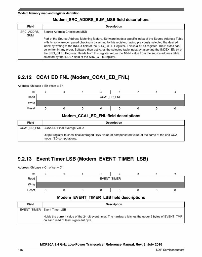
Modem_SRC_ADDRS_SUM_MSB field descriptions
Field Description
SRC_ADDRS_SUM
Source Address Checksum MSB
Part of the Source Address Matching feature. Software loads a specific index of the Source Address Tablewith its software-computed checksum by writing to this register, having previously selected the desiredindex by writing to the INDEX field of the SRC_CTRL Register. This is a 16 bit register. The 2 bytes canbe written in any order. Software then activates the selected table index by asserting the INDEX_EN bit ofthe SRC_CTRL Register. Reads from this register return the 16-bit value from the source address tableselected by the INDEX field of the SRC_CTRL register.
9.2.12 CCA1 ED FNL (Modem_CCA1_ED_FNL)
Address: 0h base + Bh offset = Bh
Bit 7 6 5 4 3 2 1 0
Read CCA1_ED_FNL
Write
Reset 0 0 0 0 0 0 0 0
Modem_CCA1_ED_FNL field descriptions
Field Description
CCA1_ED_FNL CCA1/ED Final Average Value
Output register to show final averaged RSSI value or compensated value of the same at the end CCAmode1/ED computations.
9.2.13 Event Timer LSB (Modem_EVENT_TIMER_LSB)
Address: 0h base + Ch offset = Ch
Bit 7 6 5 4 3 2 1 0
Read EVENT_TIMER
Write
Reset 0 0 0 0 0 0 0 0
Modem_EVENT_TIMER_LSB field descriptions
Field Description
EVENT_TIMER Event Timer LSB
Holds the current value of the 24-bit event timer. The hardware latches the upper 2 bytes of EVENT_TMRon each read of least signficant byte.
Modem Memory map and register definition
MCR20A 2.4 GHz Low-Power Transceiver Reference Manual, Rev. 3, July 2016
146 NXP Semiconductors
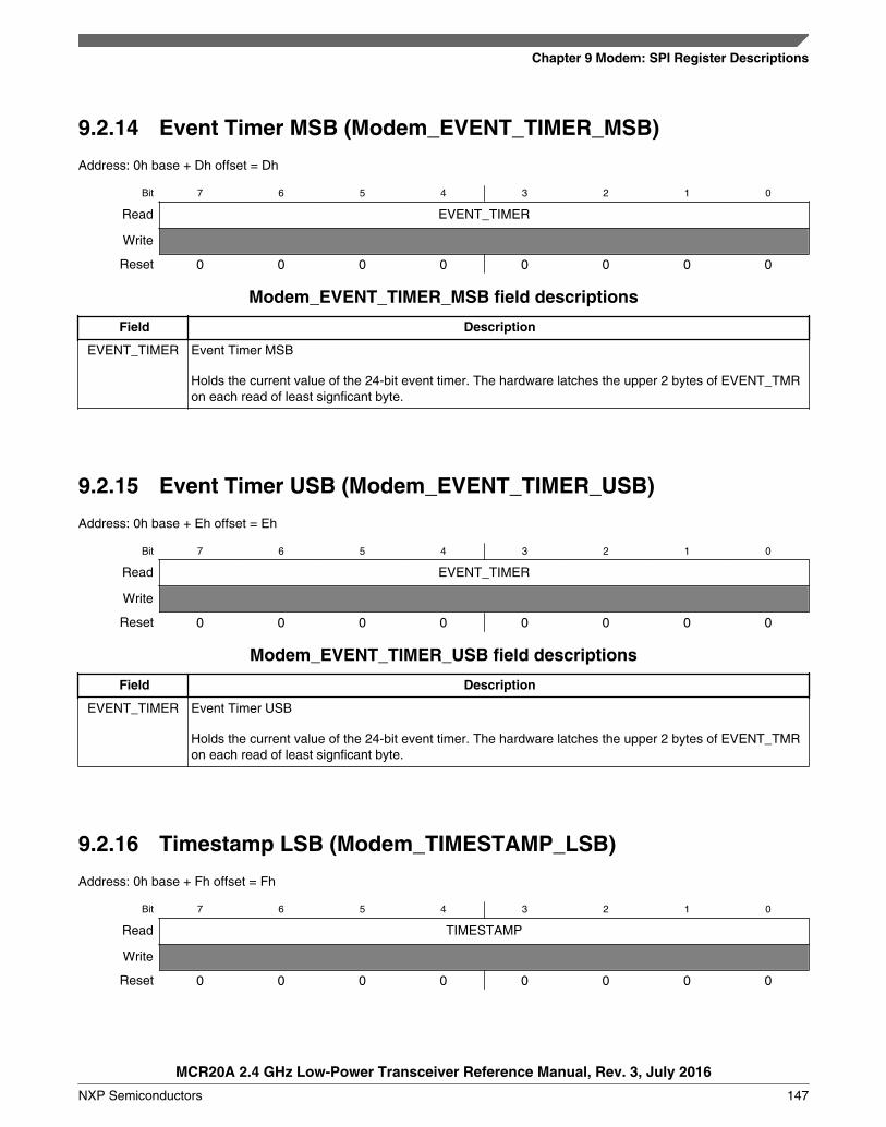
9.2.14 Event Timer MSB (Modem_EVENT_TIMER_MSB)
Address: 0h base + Dh offset = Dh
Bit 7 6 5 4 3 2 1 0
Read EVENT_TIMER
Write
Reset 0 0 0 0 0 0 0 0
Modem_EVENT_TIMER_MSB field descriptions
Field Description
EVENT_TIMER Event Timer MSB
Holds the current value of the 24-bit event timer. The hardware latches the upper 2 bytes of EVENT_TMRon each read of least signficant byte.
9.2.15 Event Timer USB (Modem_EVENT_TIMER_USB)
Address: 0h base + Eh offset = Eh
Bit 7 6 5 4 3 2 1 0
Read EVENT_TIMER
Write
Reset 0 0 0 0 0 0 0 0
Modem_EVENT_TIMER_USB field descriptions
Field Description
EVENT_TIMER Event Timer USB
Holds the current value of the 24-bit event timer. The hardware latches the upper 2 bytes of EVENT_TMRon each read of least signficant byte.
9.2.16 Timestamp LSB (Modem_TIMESTAMP_LSB)
Address: 0h base + Fh offset = Fh
Bit 7 6 5 4 3 2 1 0
Read TIMESTAMP
Write
Reset 0 0 0 0 0 0 0 0
Chapter 9 Modem: SPI Register Descriptions
MCR20A 2.4 GHz Low-Power Transceiver Reference Manual, Rev. 3, July 2016
NXP Semiconductors 147
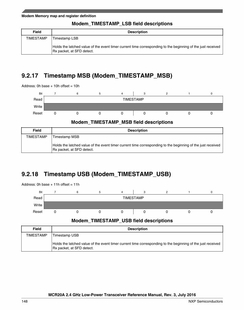
Modem_TIMESTAMP_LSB field descriptions
Field Description
TIMESTAMP Timestamp LSB
Holds the latched value of the event timer current time corresponding to the beginning of the just receivedRx packet, at SFD detect.
9.2.17 Timestamp MSB (Modem_TIMESTAMP_MSB)
Address: 0h base + 10h offset = 10h
Bit 7 6 5 4 3 2 1 0
Read TIMESTAMP
Write
Reset 0 0 0 0 0 0 0 0
Modem_TIMESTAMP_MSB field descriptions
Field Description
TIMESTAMP Timestamp MSB
Holds the latched value of the event timer current time corresponding to the beginning of the just receivedRx packet, at SFD detect.
9.2.18 Timestamp USB (Modem_TIMESTAMP_USB)
Address: 0h base + 11h offset = 11h
Bit 7 6 5 4 3 2 1 0
Read TIMESTAMP
Write
Reset 0 0 0 0 0 0 0 0
Modem_TIMESTAMP_USB field descriptions
Field Description
TIMESTAMP Timestamp USB
Holds the latched value of the event timer current time corresponding to the beginning of the just receivedRx packet, at SFD detect.
Modem Memory map and register definition
MCR20A 2.4 GHz Low-Power Transceiver Reference Manual, Rev. 3, July 2016
148 NXP Semiconductors
9.2.19 Timer 3 Compare Value LSB (Modem_T3CMP_LSB)
Address: 0h base + 12h offset = 12h
Bit 7 6 5 4 3 2 1 0
Read T3CMPWriteReset 1 1 1 1 1 1 1 1
Modem_T3CMP_LSB field descriptions
Field Description
T3CMP TMR3 Compare Value
If TMR3CMP_EN=1 and the event timer matches this value, TMR3IRQ is set.
9.2.20 Timer 3 Compare Value MSB (Modem_T3CMP_MSB)
Address: 0h base + 13h offset = 13h
Bit 7 6 5 4 3 2 1 0
Read T3CMPWriteReset 1 1 1 1 1 1 1 1
Modem_T3CMP_MSB field descriptions
Field Description
T3CMP TMR3 Compare Value
If TMR3CMP_EN=1 and the event timer matches this value, TMR3IRQ is set.
9.2.21 Timer 3 Compare Value USB (Modem_T3CMP_USB)
Address: 0h base + 14h offset = 14h
Bit 7 6 5 4 3 2 1 0
Read T3CMPWriteReset 1 1 1 1 1 1 1 1
Modem_T3CMP_USB field descriptions
Field Description
T3CMP TMR3 Compare Value
If TMR3CMP_EN=1 and the event timer matches this value, TMR3IRQ is set.
Chapter 9 Modem: SPI Register Descriptions
MCR20A 2.4 GHz Low-Power Transceiver Reference Manual, Rev. 3, July 2016
NXP Semiconductors 149
9.2.22 Timer 2-Prime Compare Value LSB(Modem_T2PRIMECMP_LSB)
Address: 0h base + 15h offset = 15h
Bit 7 6 5 4 3 2 1 0
Read T2PRIMECMPWriteReset 1 1 1 1 1 1 1 1
Modem_T2PRIMECMP_LSB field descriptions
Field Description
T2PRIMECMP TMR2-Prime Compare Value
If TMR2CMP_EN=1 and TC2PRIME_EN=1 and the lower 16 bits of the event timer matches this value,TMR2IRQ is set.
9.2.23 Timer 2-Prime Compare Value MSB(Modem_T2PRIMECMP_MSB)
Address: 0h base + 16h offset = 16h
Bit 7 6 5 4 3 2 1 0
Read T2PRIMECMPWriteReset 1 1 1 1 1 1 1 1
Modem_T2PRIMECMP_MSB field descriptions
Field Description
T2PRIMECMP TMR2-Prime Compare Value
If TMR2CMP_EN=1 and TC2PRIME_EN=1 and the lower 16 bits of the event timer matches this value,TMR2IRQ is set.
9.2.24 Timer 1 Compare Value LSB (Modem_T1CMP_LSB)
Address: 0h base + 17h offset = 17h
Bit 7 6 5 4 3 2 1 0
Read T1CMPWriteReset 1 1 1 1 1 1 1 1
Modem Memory map and register definition
MCR20A 2.4 GHz Low-Power Transceiver Reference Manual, Rev. 3, July 2016
150 NXP Semiconductors
Modem_T1CMP_LSB field descriptions
Field Description
T1CMP TMR1 Compare Value
If TMR1CMP_EN=1 and the event timer matches this value, TMR1IRQ is set.
9.2.25 Timer 1 Compare Value MSB (Modem_T1CMP_MSB)
Address: 0h base + 18h offset = 18h
Bit 7 6 5 4 3 2 1 0
Read T1CMPWriteReset 1 1 1 1 1 1 1 1
Modem_T1CMP_MSB field descriptions
Field Description
T1CMP TMR1 Compare Value
If TMR1CMP_EN=1 and the event timer matches this value, TMR1IRQ is set.
9.2.26 Timer 1 Compare Value USB (Modem_T1CMP_USB)
Address: 0h base + 19h offset = 19h
Bit 7 6 5 4 3 2 1 0
Read T1CMPWriteReset 1 1 1 1 1 1 1 1
Modem_T1CMP_USB field descriptions
Field Description
T1CMP TMR1 Compare Value
If TMR1CMP_EN=1 and the event timer matches this value, TMR1IRQ is set.
9.2.27 Timer 2 Compare Value LSB (Modem_T2CMP_LSB)
Address: 0h base + 1Ah offset = 1Ah
Bit 7 6 5 4 3 2 1 0
Read T2CMPWriteReset 1 1 1 1 1 1 1 1
Chapter 9 Modem: SPI Register Descriptions
MCR20A 2.4 GHz Low-Power Transceiver Reference Manual, Rev. 3, July 2016
NXP Semiconductors 151
Modem_T2CMP_LSB field descriptions
Field Description
T2CMP TMR2 Compare Value
If TMR2CMP_EN=1 and the event timer matches this value, TMR2IRQ is set.
9.2.28 Timer 2 Compare Value MSB (Modem_T2CMP_MSB)
Address: 0h base + 1Bh offset = 1Bh
Bit 7 6 5 4 3 2 1 0
Read T2CMPWriteReset 1 1 1 1 1 1 1 1
Modem_T2CMP_MSB field descriptions
Field Description
T2CMP TMR2 Compare Value
If TMR2CMP_EN=1 and the event timer matches this value, TMR2IRQ is set.
9.2.29 Timer 2 Compare Value USB (Modem_T2CMP_USB)
Address: 0h base + 1Ch offset = 1Ch
Bit 7 6 5 4 3 2 1 0
Read T2CMPWriteReset 1 1 1 1 1 1 1 1
Modem_T2CMP_USB field descriptions
Field Description
T2CMP TMR2 Compare Value
If TMR2CMP_EN=1 and the event timer matches this value, TMR2IRQ is set.
9.2.30 Timer 4 Compare Value LSB (Modem_T4CMP_LSB)
Address: 0h base + 1Dh offset = 1Dh
Bit 7 6 5 4 3 2 1 0
Read T4CMPWriteReset 1 1 1 1 1 1 1 1
Modem Memory map and register definition
MCR20A 2.4 GHz Low-Power Transceiver Reference Manual, Rev. 3, July 2016
152 NXP Semiconductors
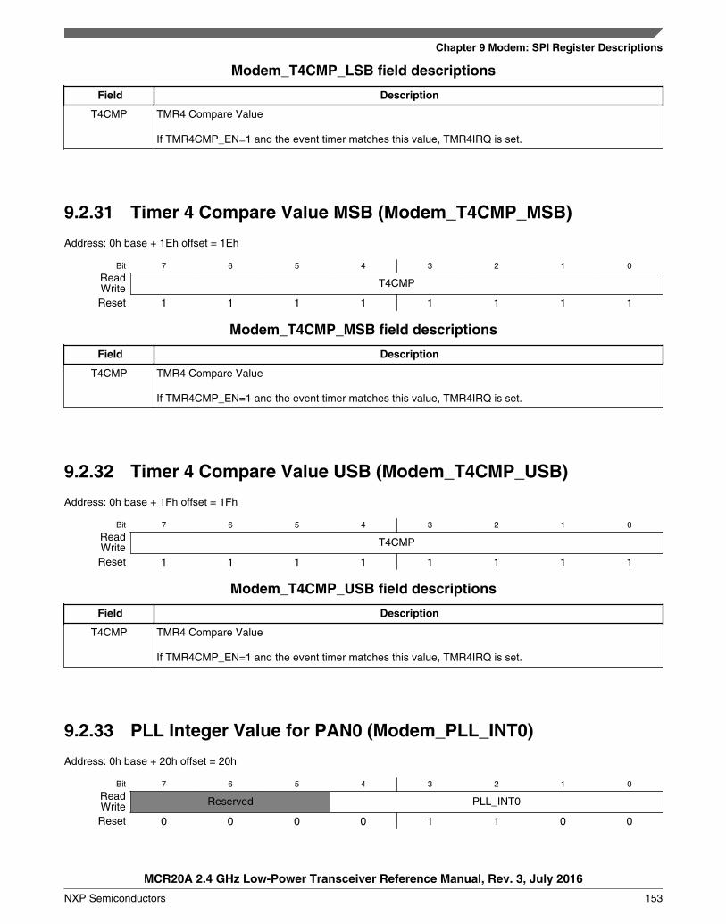
Modem_T4CMP_LSB field descriptions
Field Description
T4CMP TMR4 Compare Value
If TMR4CMP_EN=1 and the event timer matches this value, TMR4IRQ is set.
9.2.31 Timer 4 Compare Value MSB (Modem_T4CMP_MSB)
Address: 0h base + 1Eh offset = 1Eh
Bit 7 6 5 4 3 2 1 0
Read T4CMPWriteReset 1 1 1 1 1 1 1 1
Modem_T4CMP_MSB field descriptions
Field Description
T4CMP TMR4 Compare Value
If TMR4CMP_EN=1 and the event timer matches this value, TMR4IRQ is set.
9.2.32 Timer 4 Compare Value USB (Modem_T4CMP_USB)
Address: 0h base + 1Fh offset = 1Fh
Bit 7 6 5 4 3 2 1 0
Read T4CMPWriteReset 1 1 1 1 1 1 1 1
Modem_T4CMP_USB field descriptions
Field Description
T4CMP TMR4 Compare Value
If TMR4CMP_EN=1 and the event timer matches this value, TMR4IRQ is set.
9.2.33 PLL Integer Value for PAN0 (Modem_PLL_INT0)
Address: 0h base + 20h offset = 20h
Bit 7 6 5 4 3 2 1 0
Read Reserved PLL_INT0WriteReset 0 0 0 0 1 1 0 0
Chapter 9 Modem: SPI Register Descriptions
MCR20A 2.4 GHz Low-Power Transceiver Reference Manual, Rev. 3, July 2016
NXP Semiconductors 153
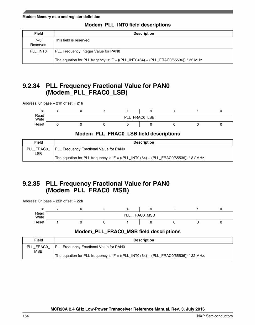
Modem_PLL_INT0 field descriptions
Field Description
7–5Reserved
This field is reserved.
PLL_INT0 PLL Frequency Integer Value for PAN0
The equation for PLL freqency is: F = ((PLL_INT0+64) + (PLL_FRAC0/65536)) * 32 MHz.
9.2.34 PLL Frequency Fractional Value for PAN0(Modem_PLL_FRAC0_LSB)
Address: 0h base + 21h offset = 21h
Bit 7 6 5 4 3 2 1 0
Read PLL_FRAC0_LSBWriteReset 0 0 0 0 0 0 0 0
Modem_PLL_FRAC0_LSB field descriptions
Field Description
PLL_FRAC0_LSB
PLL Frequency Fractional Value for PAN0
The equation for PLL frequency is: F = ((PLL_INT0+64) + (PLL_FRAC0/65536)) * 3 2MHz.
9.2.35 PLL Frequency Fractional Value for PAN0(Modem_PLL_FRAC0_MSB)
Address: 0h base + 22h offset = 22h
Bit 7 6 5 4 3 2 1 0
Read PLL_FRAC0_MSBWriteReset 1 0 0 1 0 0 0 0
Modem_PLL_FRAC0_MSB field descriptions
Field Description
PLL_FRAC0_MSB
PLL Frequency Fractional Value for PAN0
The equation for PLL frequency is: F = ((PLL_INT0+64) + (PLL_FRAC0/65536)) * 32 MHz.
Modem Memory map and register definition
MCR20A 2.4 GHz Low-Power Transceiver Reference Manual, Rev. 3, July 2016
154 NXP Semiconductors
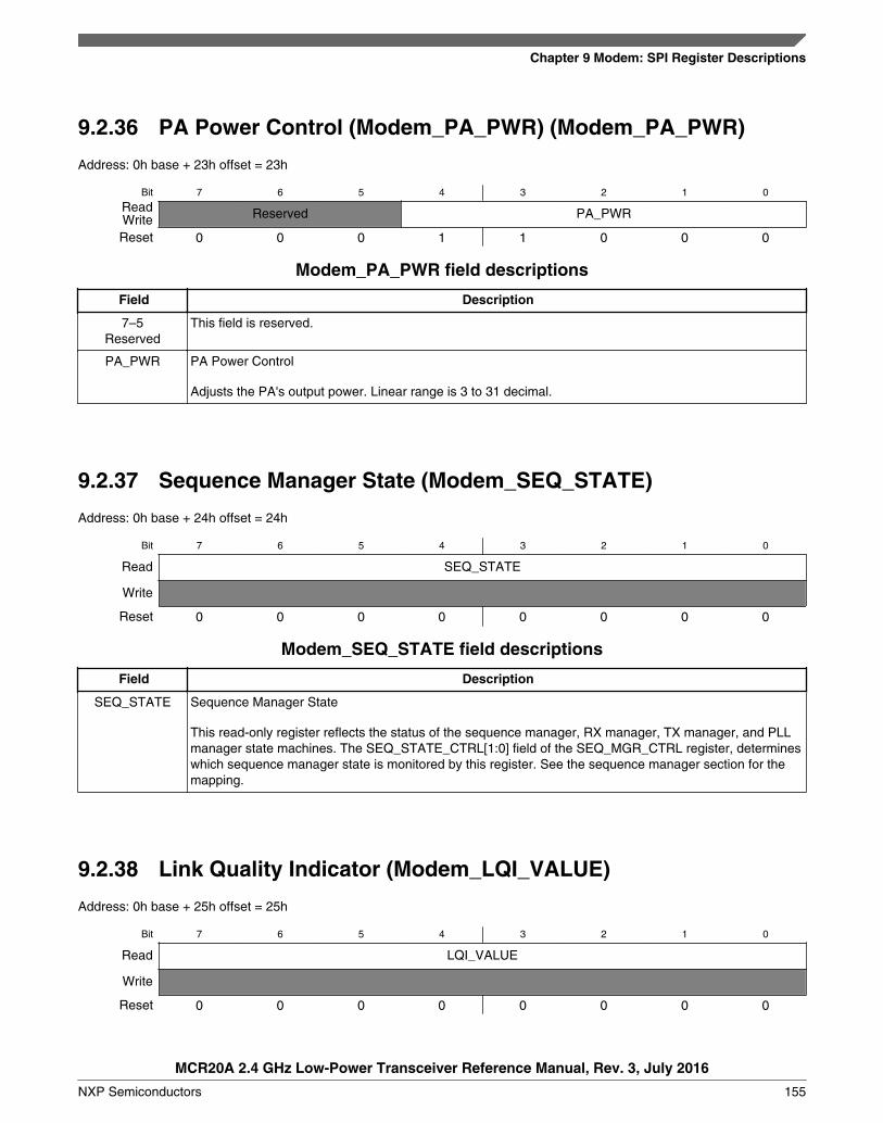
9.2.36 PA Power Control (Modem_PA_PWR) (Modem_PA_PWR)
Address: 0h base + 23h offset = 23h
Bit 7 6 5 4 3 2 1 0
Read Reserved PA_PWRWriteReset 0 0 0 1 1 0 0 0
Modem_PA_PWR field descriptions
Field Description
7–5Reserved
This field is reserved.
PA_PWR PA Power Control
Adjusts the PA's output power. Linear range is 3 to 31 decimal.
9.2.37 Sequence Manager State (Modem_SEQ_STATE)
Address: 0h base + 24h offset = 24h
Bit 7 6 5 4 3 2 1 0
Read SEQ_STATE
Write
Reset 0 0 0 0 0 0 0 0
Modem_SEQ_STATE field descriptions
Field Description
SEQ_STATE Sequence Manager State
This read-only register reflects the status of the sequence manager, RX manager, TX manager, and PLLmanager state machines. The SEQ_STATE_CTRL[1:0] field of the SEQ_MGR_CTRL register, determineswhich sequence manager state is monitored by this register. See the sequence manager section for themapping.
9.2.38 Link Quality Indicator (Modem_LQI_VALUE)
Address: 0h base + 25h offset = 25h
Bit 7 6 5 4 3 2 1 0
Read LQI_VALUE
Write
Reset 0 0 0 0 0 0 0 0
Chapter 9 Modem: SPI Register Descriptions
MCR20A 2.4 GHz Low-Power Transceiver Reference Manual, Rev. 3, July 2016
NXP Semiconductors 155
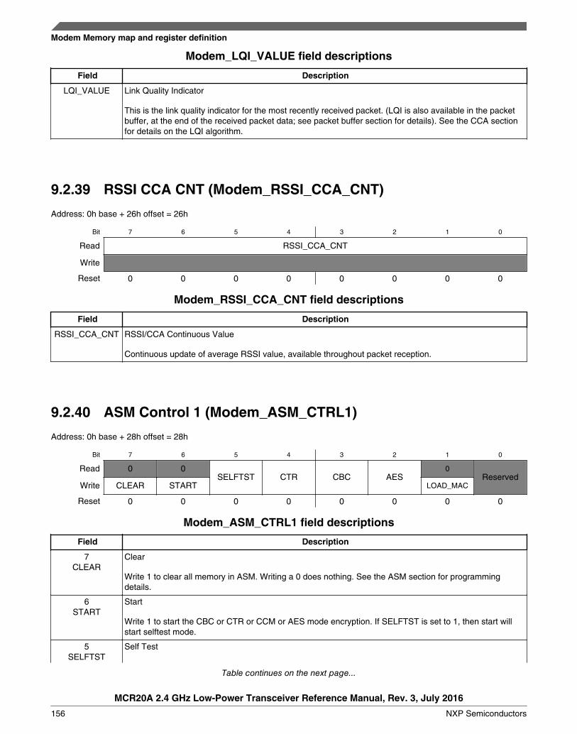
Modem_LQI_VALUE field descriptions
Field Description
LQI_VALUE Link Quality Indicator
This is the link quality indicator for the most recently received packet. (LQI is also available in the packetbuffer, at the end of the received packet data; see packet buffer section for details). See the CCA sectionfor details on the LQI algorithm.
9.2.39 RSSI CCA CNT (Modem_RSSI_CCA_CNT)
Address: 0h base + 26h offset = 26h
Bit 7 6 5 4 3 2 1 0
Read RSSI_CCA_CNT
Write
Reset 0 0 0 0 0 0 0 0
Modem_RSSI_CCA_CNT field descriptions
Field Description
RSSI_CCA_CNT RSSI/CCA Continuous Value
Continuous update of average RSSI value, available throughout packet reception.
9.2.40 ASM Control 1 (Modem_ASM_CTRL1)
Address: 0h base + 28h offset = 28h
Bit 7 6 5 4 3 2 1 0
Read 0 0SELFTST CTR CBC AES
0Reserved
Write CLEAR START LOAD_MAC
Reset 0 0 0 0 0 0 0 0
Modem_ASM_CTRL1 field descriptions
Field Description
7CLEAR
Clear
Write 1 to clear all memory in ASM. Writing a 0 does nothing. See the ASM section for programmingdetails.
6START
Start
Write 1 to start the CBC or CTR or CCM or AES mode encryption. If SELFTST is set to 1, then start willstart selftest mode.
5SELFTST
Self Test
Table continues on the next page...
Modem Memory map and register definition
MCR20A 2.4 GHz Low-Power Transceiver Reference Manual, Rev. 3, July 2016
156 NXP Semiconductors
Modem_ASM_CTRL1 field descriptions (continued)
Field Description
Write 1 to start set mode to self test (not self clearing).
0 Module not in selftest mode.1 Module in selftest mode.
4CTR
Need Name
Write 1 to put ASM into counter encryption mode.
0 Counter mode encryption will not be performed.1 Counter mode encryption will be performed.
3CBC
Need Name
Write 1 to put ASM into CBC-MAC mode.
0 CBC-MAC generation will not be performed.1 CBC-MAC generation will be performed.
2AES
Need Name
Write 1 to put ASM into AES mode.
0 AES mode encrption will not be performed.1 AES mode encrption will be performed.
1LOAD_MAC
Need Name
Write 1 to pre-load MAC with a value. Writing a 0 does nothing.
0Reserved
Reserved
This field is reserved.
9.2.41 ASM Control 2 (Modem_ASM_CTRL2)
Address: 0h base + 29h offset = 29h
Bit 7 6 5 4 3 2 1 0
ReadDATA_REG_TYPE_SELECT Reserved
LOAD_MACReserved
Write
Reset 0 0 0 0 0 0 0 0
Modem_ASM_CTRL2 field descriptions
Field Description
7–5DATA_REG_
TYPE_SELECT
Data Register Type Select
This register selects the type of data to be written to or read from the 16x8 Data register field.
000 Key: The 16 AES Data register holds the key used for encryption.001 Data: The 16 AES Data register hold the data to be encrypted or decrypted010 CTR: The 16 AES Data register hold the counter value used to encrypt the data in counter mode.
Table continues on the next page...
Chapter 9 Modem: SPI Register Descriptions
MCR20A 2.4 GHz Low-Power Transceiver Reference Manual, Rev. 3, July 2016
NXP Semiconductors 157
Modem_ASM_CTRL2 field descriptions (continued)
Field Description
011 CTR Result: The 16 AES Data register hold the counter mode encyption result100 CBC Result: The 16 AES Data register hold CBC-MAC generated results.101 MAC: The 16 AES Data register hold the starting value for CBC-MAC generation.110 AES Result: The 16 AES Data register hold the plain AES mode encryption result.111 Reserved.
4–2Reserved
Reserved
This field is reserved.
1LOAD_MAC
Test Pass
If this bit is 1 then the hardware passed the self test. If self test fails then the module is not usable and theoutputs will be set to all 0. The default state for this bit is 0. The software must initiate a self test before themodule can be used.
0Reserved
Reserved
This field is reserved.
9.2.42 ASM Data (Modem_ASM_DATAn)
Address: 0h base + 2Ah offset + (1d × i), where i=0d to 15d
Bit 7 6 5 4 3 2 1 0
Read ASM_DATAWriteReset 0 0 0 0 0 0 0 0
Modem_ASM_DATAn field descriptions
Field Description
ASM_DATA ASM Data
The 16x8 AES Data registers (128 bits) block serve as the interface between the ASM’s internal memorysegments and the external MCU. The destination or source of the data in these registers is controlledthrough the DATA_REG_TYPE_SELECT field in ASM_CTRL2. See the ASM section for programmingdetail. Register ASM_DATA_0 contains the fields ASM_DATA[7] through ASM_DATA_[0], ASM_DATA_1contains the fields ASM_DATA[15] through ASM_DATA[8].
9.2.43 Overwrite Version Number (Modem_OVERWRITE_VER)
Address: 0h base + 3Bh offset = 3Bh
Bit 7 6 5 4 3 2 1 0
Read OVERWRITE_VERWriteReset 0 0 0 0 0 0 0 0
Modem Memory map and register definition
MCR20A 2.4 GHz Low-Power Transceiver Reference Manual, Rev. 3, July 2016
158 NXP Semiconductors
Modem_OVERWRITE_VER field descriptions
Field Description
OVERWRITE_VER
Overwrite Version Number
Contains the version number of the overwrites.h file, used by stack software to write non-default valuesinto the radio’s register map.
9.2.44 CLK_OUT Control (Modem_CLK_OUT_CTRL)
This register provides control for CLK_OUT.
Address: 0h base + 3Ch offset = 3Ch
Bit 7 6 5 4
Read CLK_OUT_EXTEND CLK_OUT_HIZ CLK_OUT_SR CLK_OUT_DSWriteReset 1 0 0 0
Bit 3 2 1 0
Read CLK_OUT_EN CLK_OUT_DIVWriteReset 1 0 0 0
Modem_CLK_OUT_CTRL field descriptions
Field Description
7CLK_OUT_EXTEND
CLK_OUT Extend
Briefly extend CLK_OUT after deassertion of CLK_OUT_EN.
0 Extends CLK_OUT for 128 clock cycles after the deassertion of CLK_OUT_EN.1 Deassertion of CLK_OUT_EN immediately stops CLK_OUT.
6CLK_OUT_HIZ
CLK_OUT High Impedence Select
Selects whether CLK_OUT is placed into high-impedence mode or output mode.
0 CLK_OUT pad is in output mode (Output Buffer Enable=1, and Input Buffer Enable=0).1 Place the CLK_OUT pad in high-impedence mode (Output Buffer Enable=0, and Input Buffer
Enable=0).
5CLK_OUT_SR
CLK_OUT Slew Rate
Enables or disables slew rate limiting for CLK_OUT pad.
0 Disable slew rate limiting for CLK_OUT pad.1 Enable slew rate limiting for CLK_OUT pad.
4CLK_OUT_DS
CLK_OUT Drive Strength
Selects the drive strength for CLK_OUT.
0 Normal drive strength for CLK_OUT pad.1 High drive strength for CLK_OUT pad.
Table continues on the next page...
Chapter 9 Modem: SPI Register Descriptions
MCR20A 2.4 GHz Low-Power Transceiver Reference Manual, Rev. 3, July 2016
NXP Semiconductors 159
Modem_CLK_OUT_CTRL field descriptions (continued)
Field Description
3CLK_OUT_EN
Transmitter Interrupt Status
Shows the status of a transmit operation. This is write a 1 to clear bit.
0 CLK_OUT pad is held at 0 (assuming CLK_OUT_HIZ=0).1 CLK_OUT pad is driven with a clock whose frequency is determined by the CLK_OUT_DIV setting.
CLK_OUT_DIV CLK_OUT Divide
If programming CLK_OUT to >8 MHz, it is advisable to set CLK_OUT_DS=1. (High drive strengthCLK_OUT pad.) The CLK_OUT frequency (if CLK_OUT_EN=1), is as follows:
000 32 MHz001 16 MHz010 8 MHz011 4 MHz100 1 MHz101 250 kHz110 62.5 kHz111 32.787 kHz (32M Hz / 976)
9.2.45 Power Modes (Modem_PWR_MODES)
This register determines the power modes.
Address: 0h base + 3Dh offset = 3Dh
Bit 7 6 5 4
ReadReserved
XTAL_READYXTALEN
Write
Reset 0 0 0 1
Bit 3 2 1 0
ReadASM_CLK_EN Reserved AUTODOZE PMC_MODE
Write
Reset 0 0 0 1
Modem_PWR_MODES field descriptions
Field Description
7–6Reserved
Reserved
This field is reserved.
5XTAL_READY
XTAL Ready
Indicates whether the 32 MHz crystal oscillator has completed its warmup and is supplying clocks to thedigital core. Read-only.
Table continues on the next page...
Modem Memory map and register definition
MCR20A 2.4 GHz Low-Power Transceiver Reference Manual, Rev. 3, July 2016
160 NXP Semiconductors
Modem_PWR_MODES field descriptions (continued)
Field Description
0 The 32 MHz crystal oscillator has not completed its warmup and is supplying clocks to the digitalcore..
1 The 32 MHz crystal oscillator has completed its warmup and is supplying clocks to the digital core.
4XTALEN
CLK_OUT Slew Rate
HIBERNATE mode can be entered by setting XTALEN=0 and PMC_MODE=0. DOZE mode can beentered by setting XTALEN=1 and PMC_MODE=0. IDLE mode can be entered by setting XTALEN=1 andPMC_MODE=1. A programmed low-to-high transition on XTALEN will cause the WAKE_IRQ andWAKE_FROM_HIB status bits to become set, after the oscillator warmup has completed (see IRQSTS2register). XTALEN=1 is mandatory for all transceiver operations, including transceiver timers.
0 Disable the 32 MHz crystal oscillator.1 Enable the 32 MHz crystal oscillator.
3ASM_CLK_EN
ASM Clock Enable.
2Reserved
Reserved
This field is reserved.
1AUTODOZE
Automatic Doze Mode
Automatic Doze mode allows the PMC operating mode to be controlled automatically by the sequencemanager. In this mode, the PMC will be in high-power mode during all transceiver sequences (i.e., Runstate), and in low power mode at all other times (i.e., Doze state). If AUTODOZE=0, then PMC operatingmode is under direct software control (PMC_MODE bit)
0 Disable Automatic Doze mode.1 Enable Automatic Doze mode.
0PMC_MODE
PMC Mode
Selects whether the PMC is in high-power mode or low-power mode.
0 PMC is in low-power mode.1 PMC is in high-power mode.
9.2.46 IAR Index (Modem_IAR_INDEX)
Address: 0h base + 3Eh offset = 3Eh
Bit 7 6 5 4 3 2 1 0
Read
Write IAR_INDEX
Reset 0 0 0 0 0 0 0 0
Modem_IAR_INDEX field descriptions
Field Description
IAR_INDEX IAR Index
Chapter 9 Modem: SPI Register Descriptions
MCR20A 2.4 GHz Low-Power Transceiver Reference Manual, Rev. 3, July 2016
NXP Semiconductors 161
Modem_IAR_INDEX field descriptions (continued)
Field Description
A pointer into Indirect Access address space. During an SPI register access, when IAR_INDEX appearsas the address in the control word (first SPI byte), the following byte will be loaded into IAR_INDEX, andthe byte after that will write (or read) a byte from the indirect access register pointed to by IAR_INDEX.Hardware will automatically increment the pointer for subsequent byte accesses within the SPI bursttransfer. See the SPI chapter for more information. Indirect Access auto-incrementing is not available inHibernate state and should not be attempted; only single-access indirect register transfers are available inHibernate. Direct address auto-incrementing is available in all power states. IAR_INDEX is not affected byany soft reset bit (see SOFT_RESET register).
9.2.47 IAR Data (Modem_IAR_DATA)
Address: 0h base + 3Fh offset = 3Fh
Bit 7 6 5 4 3 2 1 0
Read IAR_DATAWriteReset 0 0 0 0 0 0 0 0
Modem_IAR_DATA field descriptions
Field Description
IAR_DATA IAR DATA
Window into Indirect Access Space. Data byte to be written (or read) to (from) this address during anIndirect Register Access will be written to (or read from) the Indirect Register pointed to by IAR_INDEX forthe first data phase of the transfer, and the Indirect Address pointer will be automatically incremented forsubsequent data phases during the SPI burst transfer. Indirect Access auto-incrementing is not availablein Hibernate state and should not be attempted. Only single-access indirect register transfers are availablein Hibernate. Direct address auto-incrementing is available in all power states. IAR_INDEX is not affectedby any soft reset bit (see SOFT_RESET register).
The read-write access of this register is determined by the read-write access of the register in IndirectAccess space to which the IAR_INDEX is pointing.
9.3 Indirect registers memory map and register definitionThe Indirect radio registers contains many bitfields for communicating with the radio.
NOTEThe Direct and Indirect registers can be accessed only throughthe SPI interface. Direct access by a single SPI control wordand Indirect using the pointer register (IAR_INDEX) and thedata register (IAR_DATA), which occupy the last two registersin direct access; addresses 0x3E and 0x3F, respectively.
Indirect registers memory map and register definition
MCR20A 2.4 GHz Low-Power Transceiver Reference Manual, Rev. 3, July 2016
162 NXP Semiconductors
Indirect_Modem memory map
Absoluteaddress
(hex)Register name
Width(in bits)
Access Reset valueSection/
page
0 Part Identification (Indirect_Modem_PART_ID) 8 R 9.3.1/165
1 XTAL 32 MHz Trim (Indirect_Modem_XTAL_TRIM) 8 R/W 77h 9.3.2/165
3MAC PAN ID for PAN0(Indirect_Modem_MACPANID0_LSB)
8 R/W FFh 9.3.3/166
4MAC PAN ID for PAN0(Indirect_Modem_MACPANID0_MSB)
8 R/W FFh 9.3.3/166
5MAC Short Address for PAN0(Indirect_Modem_MACSHORTADDRS0_LSB)
8 R/W FFh 9.3.4/166
6MAC Short Address for PAN0(Indirect_Modem_MACSHORTADDRS0_MSB)
8 R/W FFh 9.3.4/166
7MAC Long Address for PAN0(Indirect_Modem_MACLONGADDRS0_0)
8 R/W FFh 9.3.5/167
8MAC Long Address for PAN0(Indirect_Modem_MACLONGADDRS0_1)
8 R/W FFh 9.3.5/167
9MAC Long Address for PAN0(Indirect_Modem_MACLONGADDRS0_2)
8 R/W FFh 9.3.5/167
AMAC Long Address for PAN0(Indirect_Modem_MACLONGADDRS0_3)
8 R/W FFh 9.3.5/167
BMAC Long Address for PAN0(Indirect_Modem_MACLONGADDRS0_4)
8 R/W FFh 9.3.5/167
CMAC Long Address for PAN0(Indirect_Modem_MACLONGADDRS0_5)
8 R/W FFh 9.3.5/167
DMAC Long Address for PAN0(Indirect_Modem_MACLONGADDRS0_6)
8 R/W FFh 9.3.5/167
EMAC Long Address for PAN0(Indirect_Modem_MACLONGADDRS0_7)
8 R/W FFh 9.3.5/167
FReceive Frame Filter(Indirect_Modem_RX_FRAME_FILTER)
8 R/W 0Fh 9.3.6/167
10 Frequency Integer for PAN1 (Indirect_Modem_PLL_INT1) 8 R/W 1Fh 9.3.7/168
11Frequency Fractional Value for PAN1(Indirect_Modem_PLL_FRAC1_LSB)
8 R/W FFh 9.3.8/169
12Frequency Fractional Value for PAN1(Indirect_Modem_PLL_FRAC1_MSB)
8 R/W FFh 9.3.8/169
13Frequency Fractional Value for PAN1(Indirect_Modem_MACPANID1_LSB)
8 R/W FFh 9.3.9/169
14Frequency Fractional Value for PAN1(Indirect_Modem_MACPANID1_MSB)
8 R/W FFh 9.3.9/169
15MAC Short Address for PAN1(Indirect_Modem_MACSHORTADDRS1_LSB)
8 R/W FFh 9.3.10/170
16MAC Short Address for PAN1(Indirect_Modem_MACSHORTADDRS1_MSB)
8 R/W FFh 9.3.10/170
17MAC Long Address for PAN1(Indirect_Modem_MACLONGADDRS1_0)
8 R/W FFh 9.3.11/170
Table continues on the next page...
Chapter 9 Modem: SPI Register Descriptions
MCR20A 2.4 GHz Low-Power Transceiver Reference Manual, Rev. 3, July 2016
NXP Semiconductors 163
Indirect_Modem memory map (continued)
Absoluteaddress
(hex)Register name
Width(in bits)
Access Reset valueSection/
page
18MAC Long Address for PAN1(Indirect_Modem_MACLONGADDRS1_1)
8 R/W FFh 9.3.11/170
19MAC Long Address for PAN1(Indirect_Modem_MACLONGADDRS1_2)
8 R/W FFh 9.3.11/170
1AMAC Long Address for PAN1(Indirect_Modem_MACLONGADDRS1_3)
8 R/W FFh 9.3.11/170
1BMAC Long Address for PAN1(Indirect_Modem_MACLONGADDRS1_4)
8 R/W FFh 9.3.11/170
1CMAC Long Address for PAN1(Indirect_Modem_MACLONGADDRS1_5)
8 R/W FFh 9.3.11/170
1DMAC Long Address for PAN1(Indirect_Modem_MACLONGADDRS1_6)
8 R/W FFh 9.3.11/170
1EMAC Long Address for PAN1(Indirect_Modem_MACLONGADDRS1_7)
8 R/W FFh 9.3.11/170
1F Dual PAN Control (Indirect_Modem_DUAL_PAN_CTRL) 8 R/W FFh 9.3.12/171
20Channel Frequency Dwell Time(Indirect_Modem_DUAL_PAN_DWELL)
8 R/W 00h 9.3.13/172
21 Dual PAN Status (Indirect_Modem_DUAL_PAN_STS) 8 R 00h 9.3.14/172
22Clear Channel Assessment 1 Threshold(Indirect_Modem_CCA1_THRESH)
8 R/W 4Bh 9.3.15/173
23Clear Channel Assessment / ED Offset Computation(Indirect_Modem_CCA1_ED_OFFSET_COMP)
8 R/W 6Dh 9.3.16/174
24LQI Offset Computation(Indirect_Modem_LQI_OFFSET_COMP)
8 R/W 24h 9.3.17/174
25 CCA Control (Indirect_Modem_CCA_CTRL) 8 R/W 5Fh 9.3.18/174
26Clear Channel Assessment 2 Threshold Peak Compare(Indirect_Modem_CCA2_CORR_PEAKS)
8 R/W 60h 9.3.19/175
27Clear Channel Assessment 2 Threshold(Indirect_Modem_CCA2_THRESH)
8 R/W 82h 9.3.20/176
28 TMR PRESCALE (Indirect_Modem_TMR_PRESCALE) 8 R/W 03h 9.3.21/176
2A GPIO Data (Indirect_Modem_GPIO_DATA) 8 R/W 00h 9.3.22/177
2B GPIO Direction Control (Indirect_Modem_GPIO_DIR) 8 R/W 00h 9.3.23/178
2C GPIO Pullup Enable (Indirect_Modem_GPIO_PUL_EN) 8 R/W FFh 9.3.24/179
2D GPIO Pullup Select (Indirect_Modem_GPIO_SEL) 8 R/W FFh 9.3.25/181
2E GPIO Drive Strength (Indirect_Modem_GPIO_DS) 8 R/W FFh 9.3.26/182
30 Antenna Control (Indirect_Modem_ANT_PAD_CTRL) 8 R/W 08h 9.3.27/183
31Miscellaneous Pad Control(Indirect_Modem_MISC_PAD_CTRL)
8 R/W 1Ah 9.3.28/185
35 RX_BYTE_COUNT (Indirect_Modem_RX_BYTE_COUNT) 8 R 00h 9.3.29/185
36 RX_WTR_MARK (Indirect_Modem_RX_WTR_MARK) 8 R/W FFh 9.3.30/186
38 TXDELAY (Indirect_Modem_TXDELAY) 8 R/W 00h 9.3.31/186
39 ACKDELAY (Indirect_Modem_ACKDELAY) 8 R/W 3Dh 9.3.32/187
Table continues on the next page...
Indirect registers memory map and register definition
MCR20A 2.4 GHz Low-Power Transceiver Reference Manual, Rev. 3, July 2016
164 NXP Semiconductors
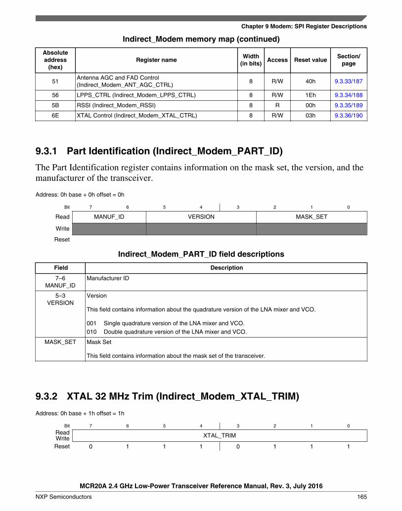
Indirect_Modem memory map (continued)
Absoluteaddress
(hex)Register name
Width(in bits)
Access Reset valueSection/
page
51Antenna AGC and FAD Control(Indirect_Modem_ANT_AGC_CTRL)
8 R/W 40h 9.3.33/187
56 LPPS_CTRL (Indirect_Modem_LPPS_CTRL) 8 R/W 1Eh 9.3.34/188
5B RSSI (Indirect_Modem_RSSI) 8 R 00h 9.3.35/189
6E XTAL Control (Indirect_Modem_XTAL_CTRL) 8 R/W 03h 9.3.36/190
9.3.1 Part Identification (Indirect_Modem_PART_ID)
The Part Identification register contains information on the mask set, the version, and themanufacturer of the transceiver.
Address: 0h base + 0h offset = 0h
Bit 7 6 5 4 3 2 1 0
Read MANUF_ID VERSION MASK_SET
Write
Reset
Indirect_Modem_PART_ID field descriptions
Field Description
7–6MANUF_ID
Manufacturer ID
5–3VERSION
Version
This field contains information about the quadrature version of the LNA mixer and VCO.
001 Single quadrature version of the LNA mixer and VCO.010 Double quadrature version of the LNA mixer and VCO.
MASK_SET Mask Set
This field contains information about the mask set of the transceiver.
9.3.2 XTAL 32 MHz Trim (Indirect_Modem_XTAL_TRIM)
Address: 0h base + 1h offset = 1h
Bit 7 6 5 4 3 2 1 0
Read XTAL_TRIMWriteReset 0 1 1 1 0 1 1 1
Chapter 9 Modem: SPI Register Descriptions
MCR20A 2.4 GHz Low-Power Transceiver Reference Manual, Rev. 3, July 2016
NXP Semiconductors 165
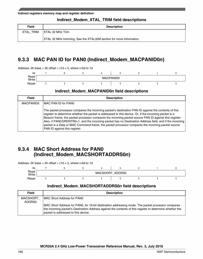
Indirect_Modem_XTAL_TRIM field descriptions
Field Description
XTAL_TRIM XTAL 32 MHz Trim
XTAL 32 MHz trimming. See the XTAL32M section for more information.
9.3.3 MAC PAN ID for PAN0 (Indirect_Modem_MACPANID0n)
Address: 0h base + 3h offset + (1d × i), where i=0d to 1d
Bit 7 6 5 4 3 2 1 0
Read MACPANID0WriteReset 1 1 1 1 1 1 1 1
Indirect_Modem_MACPANID0n field descriptions
Field Description
MACPANID0 MAC PAN ID for PAN0
The packet processor compares the incoming packet’s destination PAN ID against the contents of thisregister to determine whether the packet is addressed to this device. Or, if the incoming packet is aBeacon frame, the packet processor compares the incoming packet source PAN ID against this register.Also, if PANCORDNTR0=1, and the incoming packet has no Destination Address field, and if the incomingpacket is a Data or MAC Command frame, the packet processor compares the incoming packet sourcePAN ID against this register.
9.3.4 MAC Short Address for PAN0(Indirect_Modem_MACSHORTADDRS0n)
Address: 0h base + 5h offset + (1d × i), where i=0d to 1d
Bit 7 6 5 4 3 2 1 0
Read MACSHORT_ADDRS0WriteReset 1 1 1 1 1 1 1 1
Indirect_Modem_MACSHORTADDRS0n field descriptions
Field Description
MACSHORT_ADDRS0
MAC Short Address for PAN0
MAC Short Address for PAN0, for 16-bit destination addressing mode. The packet processor comparesthe incoming packet’s Destination Address against the contents of this register to determine whether thepacket is addressed to this device.
Indirect registers memory map and register definition
MCR20A 2.4 GHz Low-Power Transceiver Reference Manual, Rev. 3, July 2016
166 NXP Semiconductors
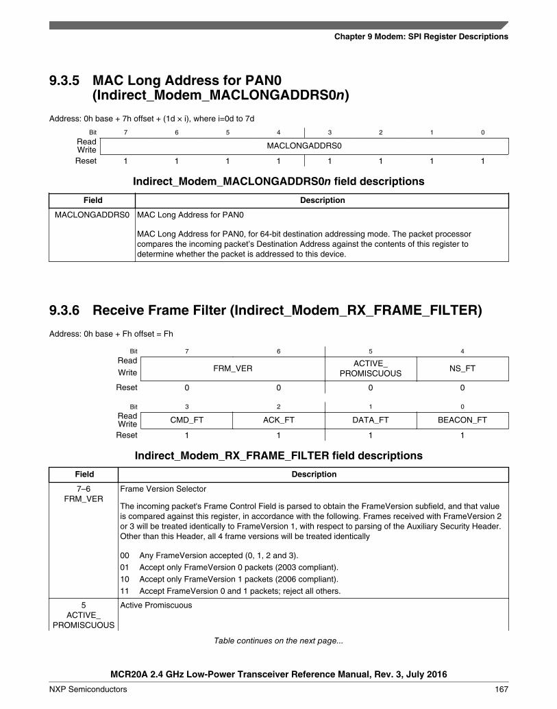
9.3.5 MAC Long Address for PAN0(Indirect_Modem_MACLONGADDRS0n)
Address: 0h base + 7h offset + (1d × i), where i=0d to 7d
Bit 7 6 5 4 3 2 1 0
Read MACLONGADDRS0WriteReset 1 1 1 1 1 1 1 1
Indirect_Modem_MACLONGADDRS0n field descriptions
Field Description
MACLONGADDRS0 MAC Long Address for PAN0
MAC Long Address for PAN0, for 64-bit destination addressing mode. The packet processorcompares the incoming packet’s Destination Address against the contents of this register todetermine whether the packet is addressed to this device.
9.3.6 Receive Frame Filter (Indirect_Modem_RX_FRAME_FILTER)
Address: 0h base + Fh offset = Fh
Bit 7 6 5 4
ReadFRM_VER
ACTIVE_PROMISCUOUS
NS_FTWrite
Reset 0 0 0 0
Bit 3 2 1 0
Read CMD_FT ACK_FT DATA_FT BEACON_FTWriteReset 1 1 1 1
Indirect_Modem_RX_FRAME_FILTER field descriptions
Field Description
7–6FRM_VER
Frame Version Selector
The incoming packet's Frame Control Field is parsed to obtain the FrameVersion subfield, and that valueis compared against this register, in accordance with the following. Frames received with FrameVersion 2or 3 will be treated identically to FrameVersion 1, with respect to parsing of the Auxiliary Security Header.Other than this Header, all 4 frame versions will be treated identically
00 Any FrameVersion accepted (0, 1, 2 and 3).01 Accept only FrameVersion 0 packets (2003 compliant).10 Accept only FrameVersion 1 packets (2006 compliant).11 Accept FrameVersion 0 and 1 packets; reject all others.
5ACTIVE_
PROMISCUOUS
Active Promiscuous
Table continues on the next page...
Chapter 9 Modem: SPI Register Descriptions
MCR20A 2.4 GHz Low-Power Transceiver Reference Manual, Rev. 3, July 2016
NXP Semiconductors 167

Indirect_Modem_RX_FRAME_FILTER field descriptions (continued)
Field Description
0 Normal operation (default).1 Provide data indication on all received packets under the same rules that apply in Promiscuous mode,
however acknowledge those packets under rules that apply in non-Promiscuous mode
4NS_FT
Not-Specified (Reserved) Frame Type
Field determines whether Not-Specified (Reserved) frame types are enabled.
0 Reject all reserved frames.1 Not-Specified (reserved) frame type enabled. No packet filtering is performed, except for frame length
checking (FrameLength is greater than or equal to 5 and FrameLength is less than or equal to 127).
3CMD_FT
MAC Command Frame Type
Field determines whether MAC Command frame types are enabled.
0 Reject all MAC Command frames.1 MAC Command frame type enabled.
2ACK_FT
Acknowledge Frame Type
Field determines whether Acknowledge frame types are enabled.
0 Reject all Acknowledge frames.1 Acknowledge frame type enabled.
1DATA_FT
Data Frame Type
Field determines whether Data frame types are enabled.
0 Reject all Data frames.1 Data frame type enabled.
0BEACON_FT
Beacon Frame Type
Field determines whether Beacon frame types are enabled.
0 Reject all Beacon frames.1 Beacon frame type enabled.
9.3.7 Frequency Integer for PAN1 (Indirect_Modem_PLL_INT1)
Address: 0h base + 10h offset = 10h
Bit 7 6 5 4 3 2 1 0
Read Reserved PLL_INT1WriteReset 0 0 0 1 1 1 1 1
Indirect_Modem_PLL_INT1 field descriptions
Field Description
7–5RESERVED
This field is reserved.
Table continues on the next page...
Indirect registers memory map and register definition
MCR20A 2.4 GHz Low-Power Transceiver Reference Manual, Rev. 3, July 2016
168 NXP Semiconductors
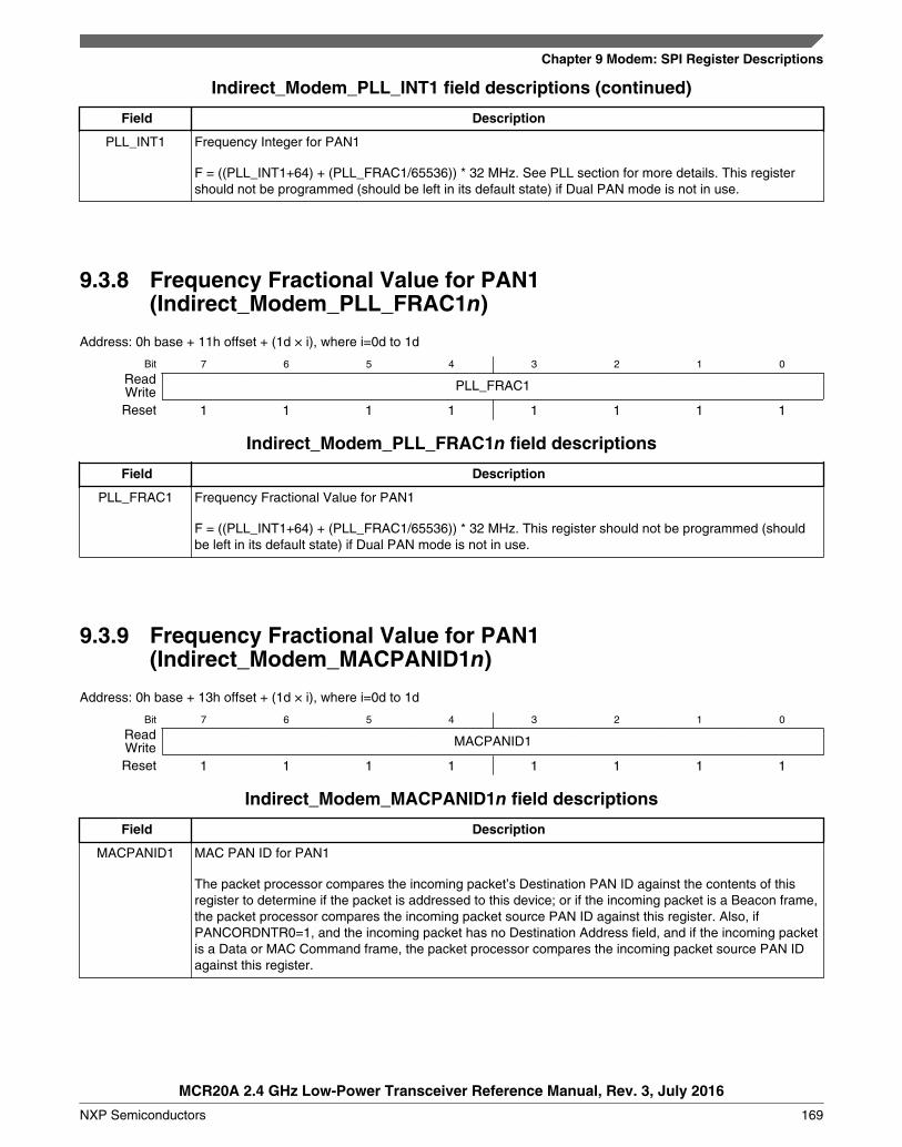
Indirect_Modem_PLL_INT1 field descriptions (continued)
Field Description
PLL_INT1 Frequency Integer for PAN1
F = ((PLL_INT1+64) + (PLL_FRAC1/65536)) * 32 MHz. See PLL section for more details. This registershould not be programmed (should be left in its default state) if Dual PAN mode is not in use.
9.3.8 Frequency Fractional Value for PAN1(Indirect_Modem_PLL_FRAC1n)
Address: 0h base + 11h offset + (1d × i), where i=0d to 1d
Bit 7 6 5 4 3 2 1 0
Read PLL_FRAC1WriteReset 1 1 1 1 1 1 1 1
Indirect_Modem_PLL_FRAC1n field descriptions
Field Description
PLL_FRAC1 Frequency Fractional Value for PAN1
F = ((PLL_INT1+64) + (PLL_FRAC1/65536)) * 32 MHz. This register should not be programmed (shouldbe left in its default state) if Dual PAN mode is not in use.
9.3.9 Frequency Fractional Value for PAN1(Indirect_Modem_MACPANID1n)
Address: 0h base + 13h offset + (1d × i), where i=0d to 1d
Bit 7 6 5 4 3 2 1 0
Read MACPANID1WriteReset 1 1 1 1 1 1 1 1
Indirect_Modem_MACPANID1n field descriptions
Field Description
MACPANID1 MAC PAN ID for PAN1
The packet processor compares the incoming packet’s Destination PAN ID against the contents of thisregister to determine if the packet is addressed to this device; or if the incoming packet is a Beacon frame,the packet processor compares the incoming packet source PAN ID against this register. Also, ifPANCORDNTR0=1, and the incoming packet has no Destination Address field, and if the incoming packetis a Data or MAC Command frame, the packet processor compares the incoming packet source PAN IDagainst this register.
Chapter 9 Modem: SPI Register Descriptions
MCR20A 2.4 GHz Low-Power Transceiver Reference Manual, Rev. 3, July 2016
NXP Semiconductors 169
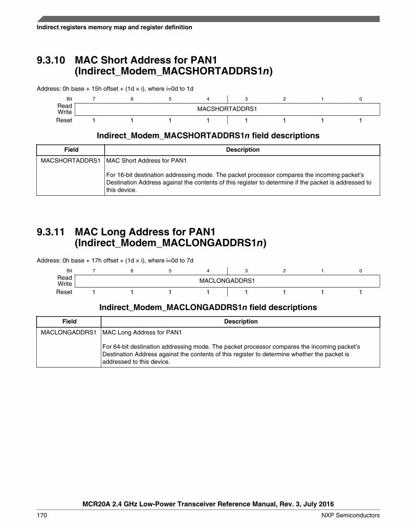
9.3.10 MAC Short Address for PAN1(Indirect_Modem_MACSHORTADDRS1n)
Address: 0h base + 15h offset + (1d × i), where i=0d to 1d
Bit 7 6 5 4 3 2 1 0
Read MACSHORTADDRS1WriteReset 1 1 1 1 1 1 1 1
Indirect_Modem_MACSHORTADDRS1n field descriptions
Field Description
MACSHORTADDRS1 MAC Short Address for PAN1
For 16-bit destination addressing mode. The packet processor compares the incoming packet’sDestination Address against the contents of this register to determine if the packet is addressed tothis device.
9.3.11 MAC Long Address for PAN1(Indirect_Modem_MACLONGADDRS1n)
Address: 0h base + 17h offset + (1d × i), where i=0d to 7d
Bit 7 6 5 4 3 2 1 0
Read MACLONGADDRS1WriteReset 1 1 1 1 1 1 1 1
Indirect_Modem_MACLONGADDRS1n field descriptions
Field Description
MACLONGADDRS1 MAC Long Address for PAN1
For 64-bit destination addressing mode. The packet processor compares the incoming packet’sDestination Address against the contents of this register to determine whether the packet isaddressed to this device.
Indirect registers memory map and register definition
MCR20A 2.4 GHz Low-Power Transceiver Reference Manual, Rev. 3, July 2016
170 NXP Semiconductors
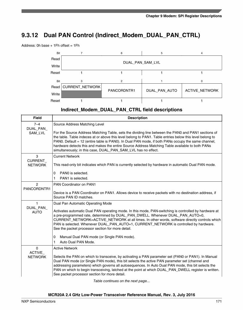
9.3.12 Dual PAN Control (Indirect_Modem_DUAL_PAN_CTRL)
Address: 0h base + 1Fh offset = 1Fh
Bit 7 6 5 4
ReadDUAL_PAN_SAM_LVL
Write
Reset 1 1 1 1
Bit 3 2 1 0
Read CURRENT_NETWORKPANCORDNTR1 DUAL_PAN_AUTO ACTIVE_NETWORK
Write
Reset 1 1 1 1
Indirect_Modem_DUAL_PAN_CTRL field descriptions
Field Description
7–4DUAL_PAN_
SAM_LVL
Source Address Matching Level
For the Source Address Matching Table, sets the dividing line between the PAN0 and PAN1 sections ofthe table. Table indeces at or above this level belong to PAN1. Table entries below this level belong toPAN0. Default = 12 (entire table is PAN0). In Dual PAN mode, if both PANs occupy the same channel,hardware detects this and makes the entire Source Address Matching Table available to both PANssimultaneously; in this case, DUAL_PAN_SAM_LVL has no effect.
3CURRENT_NETWORK
Current Network
This read-only bit indicates which PAN is currently selected by hardware in automatic Dual PAN mode.
0 PAN0 is selected.1 PAN1 is selected.
2PANCORDNTR1
PAN Coordinator on PAN1
Device is a PAN Coordinator on PAN1. Allows device to receive packets with no destination address, ifSource PAN ID matches.
1DUAL_PAN_
AUTO
Dual Pan Automatic Operating Mode
Activates automatic Dual PAN operating mode. In this mode, PAN-switching is controlled by hardware ata pre-programmed rate, determined by DUAL_PAN_DWELL. Whenever DUAL_PAN_AUTO=0,CURRENT_NETWORK=ACTIVE_NETWORK at all times. In other words, software directly controls whichPAN is selected. Whenever DUAL_PAN_AUTO=1, CURRENT_NETWORK is controlled by hardware.See the packet processor section for more detail.
0 Manual Dual PAN mode (or Single PAN mode).1 Auto Dual PAN Mode.
0ACTIVE_
NETWORK
Active Network
Selects the PAN on which to transceive, by activating a PAN parameter set (PAN0 or PAN1). In ManualDual PAN mode (or Single PAN mode), this bit selects the active PAN parameter set (channel andaddressing parameters) which governs all autosequences. In Auto Dual PAN mode, this bit selects thePAN on which to begin transceiving, latched at the point at which DUAL_PAN_DWELL register is written.See packet processor section for more detail.
Table continues on the next page...
Chapter 9 Modem: SPI Register Descriptions
MCR20A 2.4 GHz Low-Power Transceiver Reference Manual, Rev. 3, July 2016
NXP Semiconductors 171
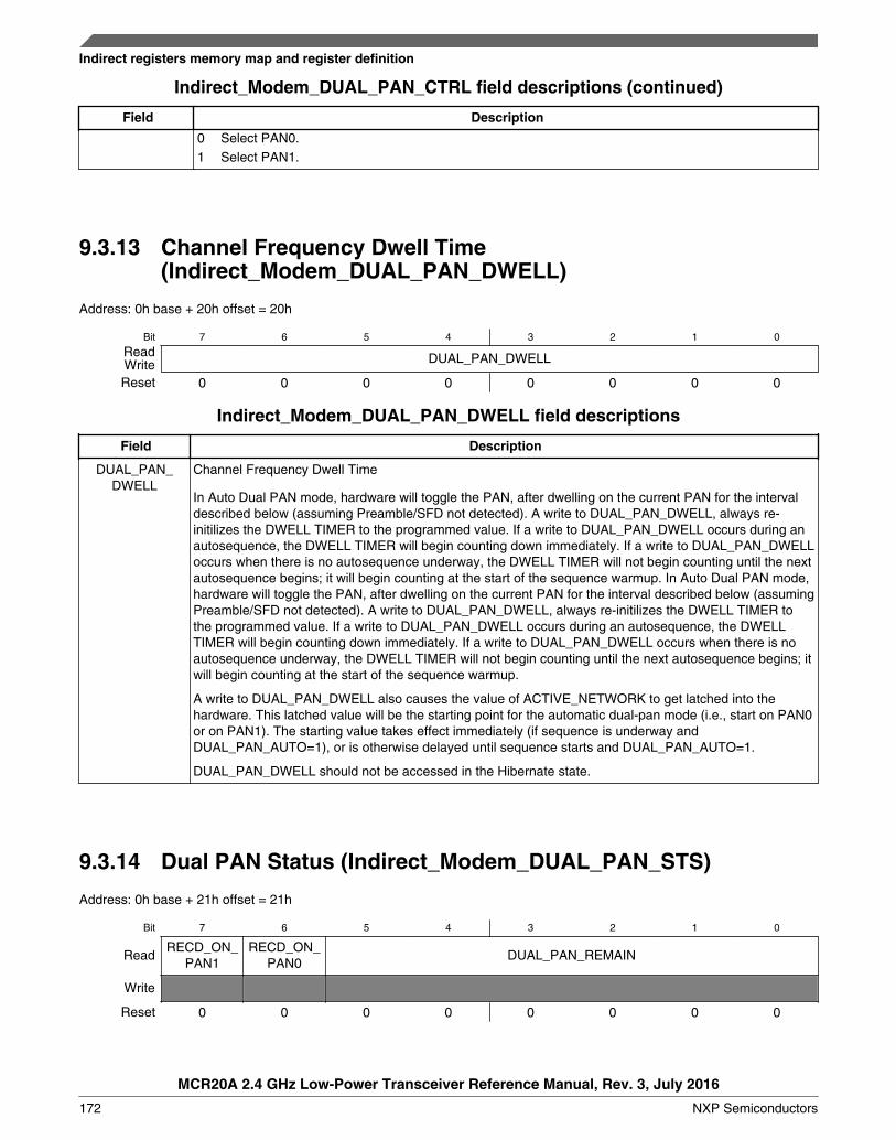
Indirect_Modem_DUAL_PAN_CTRL field descriptions (continued)
Field Description
0 Select PAN0.1 Select PAN1.
9.3.13 Channel Frequency Dwell Time(Indirect_Modem_DUAL_PAN_DWELL)
Address: 0h base + 20h offset = 20h
Bit 7 6 5 4 3 2 1 0
Read DUAL_PAN_DWELLWriteReset 0 0 0 0 0 0 0 0
Indirect_Modem_DUAL_PAN_DWELL field descriptions
Field Description
DUAL_PAN_DWELL
Channel Frequency Dwell Time
In Auto Dual PAN mode, hardware will toggle the PAN, after dwelling on the current PAN for the intervaldescribed below (assuming Preamble/SFD not detected). A write to DUAL_PAN_DWELL, always re-initilizes the DWELL TIMER to the programmed value. If a write to DUAL_PAN_DWELL occurs during anautosequence, the DWELL TIMER will begin counting down immediately. If a write to DUAL_PAN_DWELLoccurs when there is no autosequence underway, the DWELL TIMER will not begin counting until the nextautosequence begins; it will begin counting at the start of the sequence warmup. In Auto Dual PAN mode,hardware will toggle the PAN, after dwelling on the current PAN for the interval described below (assumingPreamble/SFD not detected). A write to DUAL_PAN_DWELL, always re-initilizes the DWELL TIMER tothe programmed value. If a write to DUAL_PAN_DWELL occurs during an autosequence, the DWELLTIMER will begin counting down immediately. If a write to DUAL_PAN_DWELL occurs when there is noautosequence underway, the DWELL TIMER will not begin counting until the next autosequence begins; itwill begin counting at the start of the sequence warmup.
A write to DUAL_PAN_DWELL also causes the value of ACTIVE_NETWORK to get latched into thehardware. This latched value will be the starting point for the automatic dual-pan mode (i.e., start on PAN0or on PAN1). The starting value takes effect immediately (if sequence is underway andDUAL_PAN_AUTO=1), or is otherwise delayed until sequence starts and DUAL_PAN_AUTO=1.
DUAL_PAN_DWELL should not be accessed in the Hibernate state.
9.3.14 Dual PAN Status (Indirect_Modem_DUAL_PAN_STS)
Address: 0h base + 21h offset = 21h
Bit 7 6 5 4 3 2 1 0
ReadRECD_ON_
PAN1RECD_ON_
PAN0DUAL_PAN_REMAIN
Write
Reset 0 0 0 0 0 0 0 0
Indirect registers memory map and register definition
MCR20A 2.4 GHz Low-Power Transceiver Reference Manual, Rev. 3, July 2016
172 NXP Semiconductors
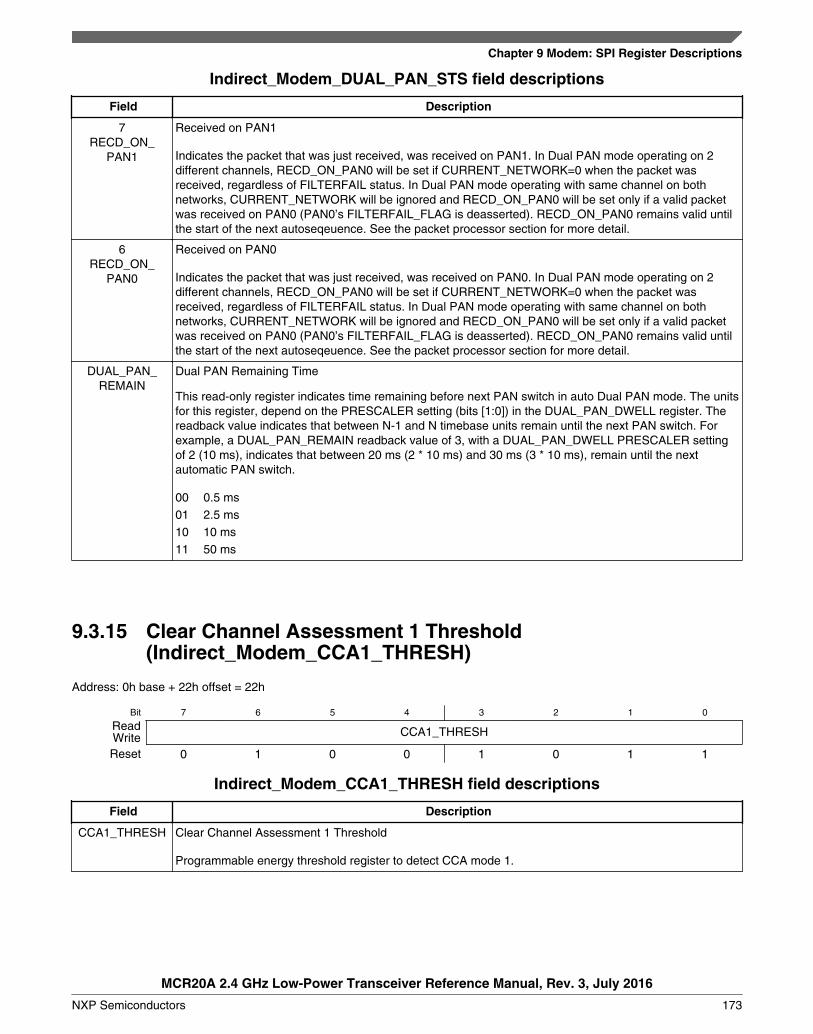
Indirect_Modem_DUAL_PAN_STS field descriptions
Field Description
7RECD_ON_
PAN1
Received on PAN1
Indicates the packet that was just received, was received on PAN1. In Dual PAN mode operating on 2different channels, RECD_ON_PAN0 will be set if CURRENT_NETWORK=0 when the packet wasreceived, regardless of FILTERFAIL status. In Dual PAN mode operating with same channel on bothnetworks, CURRENT_NETWORK will be ignored and RECD_ON_PAN0 will be set only if a valid packetwas received on PAN0 (PAN0’s FILTERFAIL_FLAG is deasserted). RECD_ON_PAN0 remains valid untilthe start of the next autoseqeuence. See the packet processor section for more detail.
6RECD_ON_
PAN0
Received on PAN0
Indicates the packet that was just received, was received on PAN0. In Dual PAN mode operating on 2different channels, RECD_ON_PAN0 will be set if CURRENT_NETWORK=0 when the packet wasreceived, regardless of FILTERFAIL status. In Dual PAN mode operating with same channel on bothnetworks, CURRENT_NETWORK will be ignored and RECD_ON_PAN0 will be set only if a valid packetwas received on PAN0 (PAN0’s FILTERFAIL_FLAG is deasserted). RECD_ON_PAN0 remains valid untilthe start of the next autoseqeuence. See the packet processor section for more detail.
DUAL_PAN_REMAIN
Dual PAN Remaining Time
This read-only register indicates time remaining before next PAN switch in auto Dual PAN mode. The unitsfor this register, depend on the PRESCALER setting (bits [1:0]) in the DUAL_PAN_DWELL register. Thereadback value indicates that between N-1 and N timebase units remain until the next PAN switch. Forexample, a DUAL_PAN_REMAIN readback value of 3, with a DUAL_PAN_DWELL PRESCALER settingof 2 (10 ms), indicates that between 20 ms (2 * 10 ms) and 30 ms (3 * 10 ms), remain until the nextautomatic PAN switch.
00 0.5 ms01 2.5 ms10 10 ms11 50 ms
9.3.15 Clear Channel Assessment 1 Threshold(Indirect_Modem_CCA1_THRESH)
Address: 0h base + 22h offset = 22h
Bit 7 6 5 4 3 2 1 0
Read CCA1_THRESHWriteReset 0 1 0 0 1 0 1 1
Indirect_Modem_CCA1_THRESH field descriptions
Field Description
CCA1_THRESH Clear Channel Assessment 1 Threshold
Programmable energy threshold register to detect CCA mode 1.
Chapter 9 Modem: SPI Register Descriptions
MCR20A 2.4 GHz Low-Power Transceiver Reference Manual, Rev. 3, July 2016
NXP Semiconductors 173
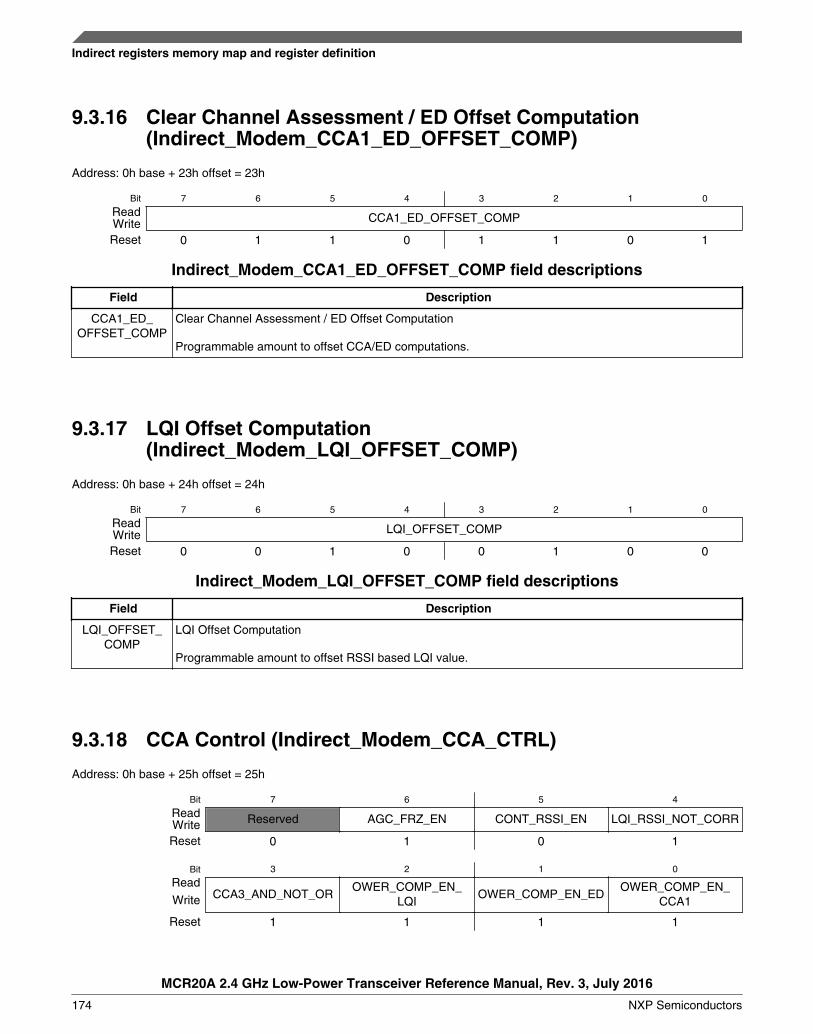
9.3.16 Clear Channel Assessment / ED Offset Computation(Indirect_Modem_CCA1_ED_OFFSET_COMP)
Address: 0h base + 23h offset = 23h
Bit 7 6 5 4 3 2 1 0
Read CCA1_ED_OFFSET_COMPWriteReset 0 1 1 0 1 1 0 1
Indirect_Modem_CCA1_ED_OFFSET_COMP field descriptions
Field Description
CCA1_ED_OFFSET_COMP
Clear Channel Assessment / ED Offset Computation
Programmable amount to offset CCA/ED computations.
9.3.17 LQI Offset Computation(Indirect_Modem_LQI_OFFSET_COMP)
Address: 0h base + 24h offset = 24h
Bit 7 6 5 4 3 2 1 0
Read LQI_OFFSET_COMPWriteReset 0 0 1 0 0 1 0 0
Indirect_Modem_LQI_OFFSET_COMP field descriptions
Field Description
LQI_OFFSET_COMP
LQI Offset Computation
Programmable amount to offset RSSI based LQI value.
9.3.18 CCA Control (Indirect_Modem_CCA_CTRL)
Address: 0h base + 25h offset = 25h
Bit 7 6 5 4
Read Reserved AGC_FRZ_EN CONT_RSSI_EN LQI_RSSI_NOT_CORRWriteReset 0 1 0 1
Bit 3 2 1 0
ReadCCA3_AND_NOT_OR
OWER_COMP_EN_LQI
OWER_COMP_EN_EDOWER_COMP_EN_
CCA1Write
Reset 1 1 1 1
Indirect registers memory map and register definition
MCR20A 2.4 GHz Low-Power Transceiver Reference Manual, Rev. 3, July 2016
174 NXP Semiconductors
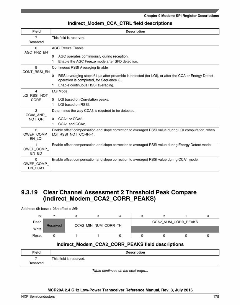
Indirect_Modem_CCA_CTRL field descriptions
Field Description
7Reserved
This field is reserved.
6AGC_FRZ_EN
AGC Freeze Enable
0 AGC operates continuously during reception.1 Enable the AGC Freeze mode after SFD detection.
5CONT_RSSI_EN
Continuous RSSI Averaging Enable
0 RSSI averaging stops 64 µs after preamble is detected (for LQI), or after the CCA or Energy Detectoperation is completed, for Sequence C.
1 Enable continuous RSSI averaging.
4LQI_RSSI_NOT_
CORR
LQI Mode
0 LQI based on Correlation peaks.1 LQI based on RSSI.
3CCA3_AND_
NOT_OR
Determines the way CCA3 is required to be detected.
0 CCA1 or CCA2.1 CCA1 and CCA2.
2OWER_COMP_
EN_LQI
Enable offset compensation and slope correction to averaged RSSI value during LQI computation, whenLQI_RSSI_NOT_CORR=1.
1OWER_COMP_
EN_ED
Enable offset compensation and slope correction to averaged RSSI value during Energy Detect mode.
0OWER_COMP_
EN_CCA1
Enable offset compensation and slope correction to averaged RSSI value during CCA1 mode.
9.3.19 Clear Channel Assessment 2 Threshold Peak Compare(Indirect_Modem_CCA2_CORR_PEAKS)
Address: 0h base + 26h offset = 26h
Bit 7 6 5 4 3 2 1 0
ReadReserved CCA2_MIN_NUM_CORR_TH
CCA2_NUM_CORR_PEAKS
Write
Reset 0 1 1 0 0 0 0 0
Indirect_Modem_CCA2_CORR_PEAKS field descriptions
Field Description
7Reserved
This field is reserved.
Table continues on the next page...
Chapter 9 Modem: SPI Register Descriptions
MCR20A 2.4 GHz Low-Power Transceiver Reference Manual, Rev. 3, July 2016
NXP Semiconductors 175
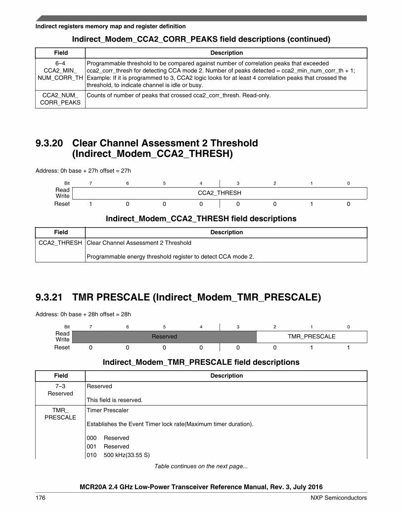
Indirect_Modem_CCA2_CORR_PEAKS field descriptions (continued)
Field Description
6–4CCA2_MIN_
NUM_CORR_TH
Programmable threshold to be compared against number of correlation peaks that exceededcca2_corr_thresh for detecting CCA mode 2. Number of peaks detected = cca2_min_num_corr_th + 1;Example: If it is programmed to 3, CCA2 logic looks for at least 4 correlation peaks that crossed thethreshold, to indicate channel is idle or busy.
CCA2_NUM_CORR_PEAKS
Counts of number of peaks that crossed cca2_corr_thresh. Read-only.
9.3.20 Clear Channel Assessment 2 Threshold(Indirect_Modem_CCA2_THRESH)
Address: 0h base + 27h offset = 27h
Bit 7 6 5 4 3 2 1 0
Read CCA2_THRESHWriteReset 1 0 0 0 0 0 1 0
Indirect_Modem_CCA2_THRESH field descriptions
Field Description
CCA2_THRESH Clear Channel Assessment 2 Threshold
Programmable energy threshold register to detect CCA mode 2.
9.3.21 TMR PRESCALE (Indirect_Modem_TMR_PRESCALE)
Address: 0h base + 28h offset = 28h
Bit 7 6 5 4 3 2 1 0
Read Reserved TMR_PRESCALEWriteReset 0 0 0 0 0 0 1 1
Indirect_Modem_TMR_PRESCALE field descriptions
Field Description
7–3Reserved
Reserved
This field is reserved.
TMR_PRESCALE
Timer Prescaler
Establishes the Event Timer lock rate(Maximum timer duration).
000 Reserved001 Reserved010 500 kHz(33.55 S)
Table continues on the next page...
Indirect registers memory map and register definition
MCR20A 2.4 GHz Low-Power Transceiver Reference Manual, Rev. 3, July 2016
176 NXP Semiconductors
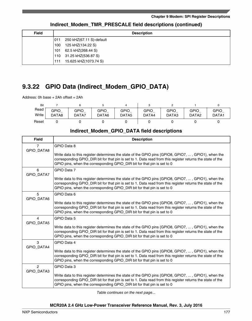
Indirect_Modem_TMR_PRESCALE field descriptions (continued)
Field Description
011 250 kHZ(67.11 S)-default100 125 kHZ(134.22 S)101 62.5 kHZ(268.44 S)110 31.25 kHZ(536.87 S)111 15.625 kHZ(1073.74 S)
9.3.22 GPIO Data (Indirect_Modem_GPIO_DATA)
Address: 0h base + 2Ah offset = 2Ah
Bit 7 6 5 4 3 2 1 0
Read GPIO_DATA8
GPIO_DATA7
GPIO_DATA6
GPIO_DATA5
GPIO_DATA4
GPIO_DATA3
GPIO_DATA2
GPIO_DATA1Write
Reset 0 0 0 0 0 0 0 0
Indirect_Modem_GPIO_DATA field descriptions
Field Description
7GPIO_DATA8
GPIO Data 8
Write data to this register determines the state of the GPIO pins {GPIO8, GPIO7, ... , GPIO1}, when thecorresponding GPIO_DIR bit for that pin is set to 1. Data read from this register returns the state of theGPIO pins, when the corresponding GPIO_DIR bit for that pin is set to 0
6GPIO_DATA7
GPIO Data 7
Write data to this register determines the state of the GPIO pins {GPIO8, GPIO7, ... , GPIO1}, when thecorresponding GPIO_DIR bit for that pin is set to 1. Data read from this register returns the state of theGPIO pins, when the corresponding GPIO_DIR bit for that pin is set to 0
5GPIO_DATA6
GPIO Data 6
Write data to this register determines the state of the GPIO pins {GPIO8, GPIO7, ... , GPIO1}, when thecorresponding GPIO_DIR bit for that pin is set to 1. Data read from this register returns the state of theGPIO pins, when the corresponding GPIO_DIR bit for that pin is set to 0
4GPIO_DATA5
GPIO Data 5
Write data to this register determines the state of the GPIO pins {GPIO8, GPIO7, ... , GPIO1}, when thecorresponding GPIO_DIR bit for that pin is set to 1. Data read from this register returns the state of theGPIO pins, when the corresponding GPIO_DIR bit for that pin is set to 0
3GPIO_DATA4
GPIO Data 4
Write data to this register determines the state of the GPIO pins {GPIO8, GPIO7, ... , GPIO1}, when thecorresponding GPIO_DIR bit for that pin is set to 1. Data read from this register returns the state of theGPIO pins, when the corresponding GPIO_DIR bit for that pin is set to 0
2GPIO_DATA3
GPIO Data 3
Write data to this register determines the state of the GPIO pins {GPIO8, GPIO7, ... , GPIO1}, when thecorresponding GPIO_DIR bit for that pin is set to 1. Data read from this register returns the state of theGPIO pins, when the corresponding GPIO_DIR bit for that pin is set to 0
Table continues on the next page...
Chapter 9 Modem: SPI Register Descriptions
MCR20A 2.4 GHz Low-Power Transceiver Reference Manual, Rev. 3, July 2016
NXP Semiconductors 177
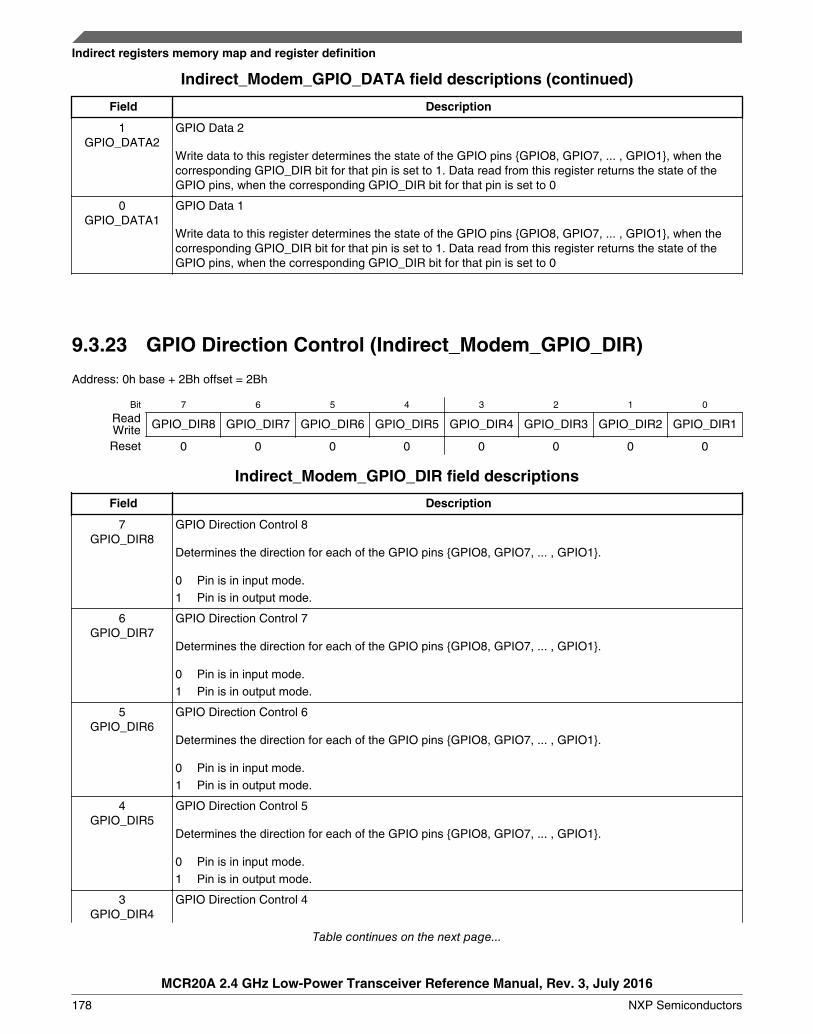
Indirect_Modem_GPIO_DATA field descriptions (continued)
Field Description
1GPIO_DATA2
GPIO Data 2
Write data to this register determines the state of the GPIO pins {GPIO8, GPIO7, ... , GPIO1}, when thecorresponding GPIO_DIR bit for that pin is set to 1. Data read from this register returns the state of theGPIO pins, when the corresponding GPIO_DIR bit for that pin is set to 0
0GPIO_DATA1
GPIO Data 1
Write data to this register determines the state of the GPIO pins {GPIO8, GPIO7, ... , GPIO1}, when thecorresponding GPIO_DIR bit for that pin is set to 1. Data read from this register returns the state of theGPIO pins, when the corresponding GPIO_DIR bit for that pin is set to 0
9.3.23 GPIO Direction Control (Indirect_Modem_GPIO_DIR)
Address: 0h base + 2Bh offset = 2Bh
Bit 7 6 5 4 3 2 1 0
Read GPIO_DIR8 GPIO_DIR7 GPIO_DIR6 GPIO_DIR5 GPIO_DIR4 GPIO_DIR3 GPIO_DIR2 GPIO_DIR1WriteReset 0 0 0 0 0 0 0 0
Indirect_Modem_GPIO_DIR field descriptions
Field Description
7GPIO_DIR8
GPIO Direction Control 8
Determines the direction for each of the GPIO pins {GPIO8, GPIO7, ... , GPIO1}.
0 Pin is in input mode.1 Pin is in output mode.
6GPIO_DIR7
GPIO Direction Control 7
Determines the direction for each of the GPIO pins {GPIO8, GPIO7, ... , GPIO1}.
0 Pin is in input mode.1 Pin is in output mode.
5GPIO_DIR6
GPIO Direction Control 6
Determines the direction for each of the GPIO pins {GPIO8, GPIO7, ... , GPIO1}.
0 Pin is in input mode.1 Pin is in output mode.
4GPIO_DIR5
GPIO Direction Control 5
Determines the direction for each of the GPIO pins {GPIO8, GPIO7, ... , GPIO1}.
0 Pin is in input mode.1 Pin is in output mode.
3GPIO_DIR4
GPIO Direction Control 4
Table continues on the next page...
Indirect registers memory map and register definition
MCR20A 2.4 GHz Low-Power Transceiver Reference Manual, Rev. 3, July 2016
178 NXP Semiconductors
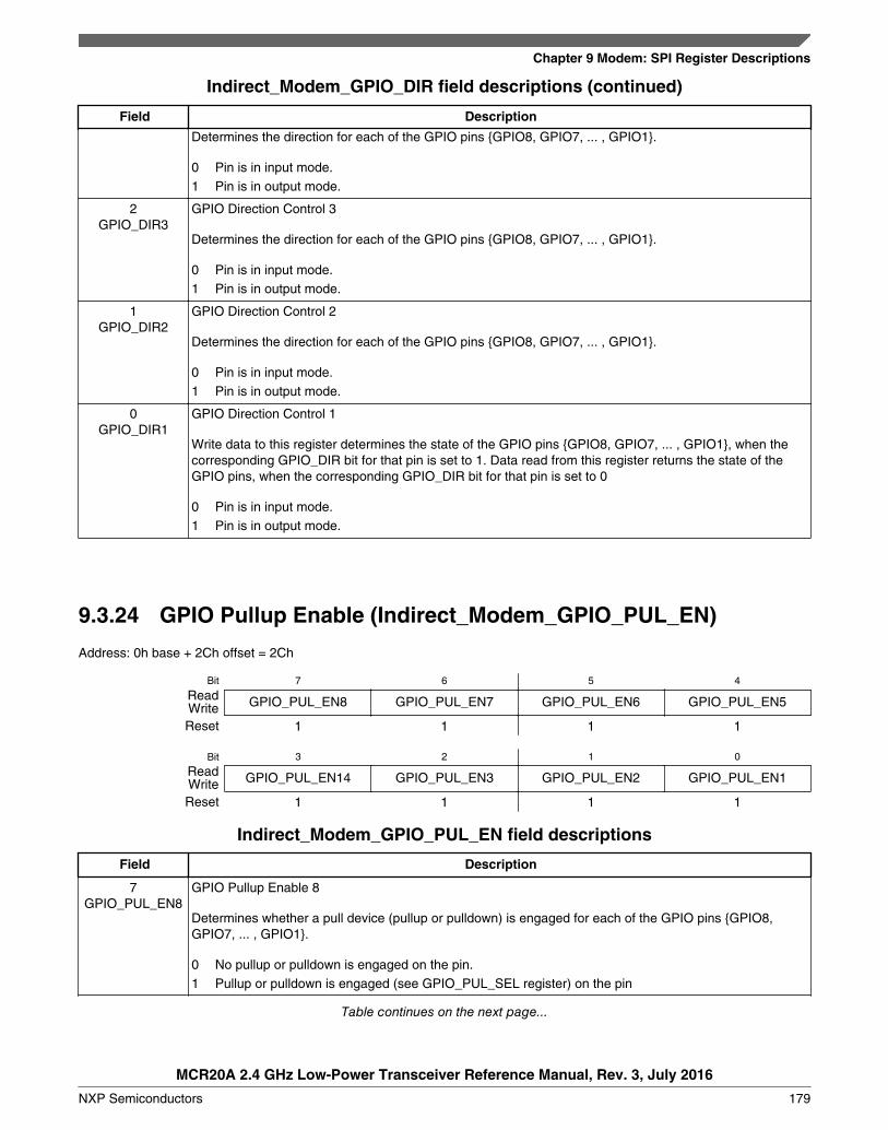
Indirect_Modem_GPIO_DIR field descriptions (continued)
Field Description
Determines the direction for each of the GPIO pins {GPIO8, GPIO7, ... , GPIO1}.
0 Pin is in input mode.1 Pin is in output mode.
2GPIO_DIR3
GPIO Direction Control 3
Determines the direction for each of the GPIO pins {GPIO8, GPIO7, ... , GPIO1}.
0 Pin is in input mode.1 Pin is in output mode.
1GPIO_DIR2
GPIO Direction Control 2
Determines the direction for each of the GPIO pins {GPIO8, GPIO7, ... , GPIO1}.
0 Pin is in input mode.1 Pin is in output mode.
0GPIO_DIR1
GPIO Direction Control 1
Write data to this register determines the state of the GPIO pins {GPIO8, GPIO7, ... , GPIO1}, when thecorresponding GPIO_DIR bit for that pin is set to 1. Data read from this register returns the state of theGPIO pins, when the corresponding GPIO_DIR bit for that pin is set to 0
0 Pin is in input mode.1 Pin is in output mode.
9.3.24 GPIO Pullup Enable (Indirect_Modem_GPIO_PUL_EN)
Address: 0h base + 2Ch offset = 2Ch
Bit 7 6 5 4
Read GPIO_PUL_EN8 GPIO_PUL_EN7 GPIO_PUL_EN6 GPIO_PUL_EN5WriteReset 1 1 1 1
Bit 3 2 1 0
Read GPIO_PUL_EN14 GPIO_PUL_EN3 GPIO_PUL_EN2 GPIO_PUL_EN1WriteReset 1 1 1 1
Indirect_Modem_GPIO_PUL_EN field descriptions
Field Description
7GPIO_PUL_EN8
GPIO Pullup Enable 8
Determines whether a pull device (pullup or pulldown) is engaged for each of the GPIO pins {GPIO8,GPIO7, ... , GPIO1}.
0 No pullup or pulldown is engaged on the pin.1 Pullup or pulldown is engaged (see GPIO_PUL_SEL register) on the pin
Table continues on the next page...
Chapter 9 Modem: SPI Register Descriptions
MCR20A 2.4 GHz Low-Power Transceiver Reference Manual, Rev. 3, July 2016
NXP Semiconductors 179

Indirect_Modem_GPIO_PUL_EN field descriptions (continued)
Field Description
6GPIO_PUL_EN7
GPIO Pullup Enable 7
Determines whether a pull device (pullup or pulldown) is engaged for each of the GPIO pins {GPIO8,GPIO7, ... , GPIO1}.
0 No pullup or pulldown is engaged on the pin.1 Pullup or pulldown is engaged (see GPIO_PUL_SEL register) on the pin
5GPIO_PUL_EN6
GPIO Pullup Enable 6
Determines whether a pull device (pullup or pulldown) is engaged for each of the GPIO pins {GPIO8,GPIO7, ... , GPIO1}.
0 No pullup or pulldown is engaged on the pin.1 Pullup or pulldown is engaged (see GPIO_PUL_SEL register) on the pin
4GPIO_PUL_EN5
GPIO Pullup Enable 5
Determines whether a pull device (pullup or pulldown) is engaged for each of the GPIO pins {GPIO8,GPIO7, ... , GPIO1}.
0 No pullup or pulldown is engaged on the pin.1 Pullup or pulldown is engaged (see GPIO_PUL_SEL register) on the pin
3GPIO_PUL_
EN14
GPIO Pullup Enable 4
Determines whether a pull device (pullup or pulldown) is engaged for each of the GPIO pins {GPIO8,GPIO7, ... , GPIO1}.
0 No pullup or pulldown is engaged on the pin.1 Pullup or pulldown is engaged (see GPIO_PUL_SEL register) on the pin
2GPIO_PUL_EN3
GPIO Pullup Enable 3
Determines whether a pull device (pullup or pulldown) is engaged for each of the GPIO pins {GPIO8,GPIO7, ... , GPIO1}.
0 No pullup or pulldown is engaged on the pin.1 Pullup or pulldown is engaged (see GPIO_PUL_SEL register) on the pin
1GPIO_PUL_EN2
GPIO Pullup Enable 2
Determines whether a pull device (pullup or pulldown) is engaged for each of the GPIO pins {GPIO8,GPIO7, ... , GPIO1}.
0 No pullup or pulldown is engaged on the pin.1 Pullup or pulldown is engaged (see GPIO_PUL_SEL register) on the pin
0GPIO_PUL_EN1
GPIO Pullup Enable 1
Determines whether a pull device (pullup or pulldown) is engaged for each of the GPIO pins {GPIO8,GPIO7, ... , GPIO1}.
0 No pullup or pulldown is engaged on the pin.1 Pullup or pulldown is engaged (see GPIO_PUL_SEL register) on the pin
Indirect registers memory map and register definition
MCR20A 2.4 GHz Low-Power Transceiver Reference Manual, Rev. 3, July 2016
180 NXP Semiconductors
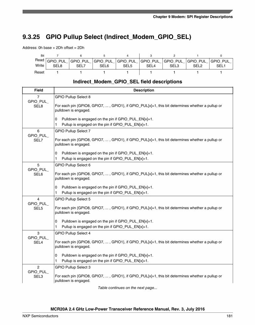
9.3.25 GPIO Pullup Select (Indirect_Modem_GPIO_SEL)
Address: 0h base + 2Dh offset = 2Dh
Bit 7 6 5 4 3 2 1 0
Read GPIO_PUL_SEL8
GPIO_PUL_SEL7
GPIO_PUL_SEL6
GPIO_PUL_SEL5
GPIO_PUL_SEL4
GPIO_PUL_SEL3
GPIO_PUL_SEL2
GPIO_PUL_SEL1Write
Reset 1 1 1 1 1 1 1 1
Indirect_Modem_GPIO_SEL field descriptions
Field Description
7GPIO_PUL_
SEL8
GPIO Pullup Select 8
For each pin {GPIO8, GPIO7, ... , GPIO1}, if GPIO_PUL[x]=1, this bit determines whether a pullup orpulldown is engaged.
0 Pulldown is engaged on the pin if GPIO_PUL_EN[x]=1.1 Pullup is engaged on the pin if GPIO_PUL_EN[x]=1.
6GPIO_PUL_
SEL7
GPIO Pullup Select 7
For each pin {GPIO8, GPIO7, ... , GPIO1}, if GPIO_PUL[x]=1, this bit determines whether a pullup orpulldown is engaged.
0 Pulldown is engaged on the pin if GPIO_PUL_EN[x]=1.1 Pullup is engaged on the pin if GPIO_PUL_EN[x]=1.
5GPIO_PUL_
SEL6
GPIO Pullup Select 6
For each pin {GPIO8, GPIO7, ... , GPIO1}, if GPIO_PUL[x]=1, this bit determines whether a pullup orpulldown is engaged.
0 Pulldown is engaged on the pin if GPIO_PUL_EN[x]=1.1 Pullup is engaged on the pin if GPIO_PUL_EN[x]=1.
4GPIO_PUL_
SEL5
GPIO Pullup Select 5
For each pin {GPIO8, GPIO7, ... , GPIO1}, if GPIO_PUL[x]=1, this bit determines whether a pullup orpulldown is engaged.
0 Pulldown is engaged on the pin if GPIO_PUL_EN[x]=1.1 Pullup is engaged on the pin if GPIO_PUL_EN[x]=1.
3GPIO_PUL_
SEL4
GPIO Pullup Select 4
For each pin {GPIO8, GPIO7, ... , GPIO1}, if GPIO_PUL[x]=1, this bit determines whether a pullup orpulldown is engaged.
0 Pulldown is engaged on the pin if GPIO_PUL_EN[x]=1.1 Pullup is engaged on the pin if GPIO_PUL_EN[x]=1.
2GPIO_PUL_
SEL3
GPIO Pullup Select 3
For each pin {GPIO8, GPIO7, ... , GPIO1}, if GPIO_PUL[x]=1, this bit determines whether a pullup orpulldown is engaged.
Table continues on the next page...
Chapter 9 Modem: SPI Register Descriptions
MCR20A 2.4 GHz Low-Power Transceiver Reference Manual, Rev. 3, July 2016
NXP Semiconductors 181
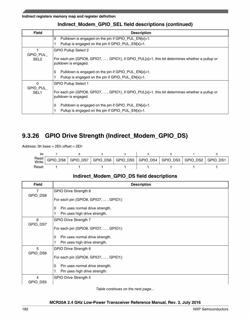
Indirect_Modem_GPIO_SEL field descriptions (continued)
Field Description
0 Pulldown is engaged on the pin if GPIO_PUL_EN[x]=1.1 Pullup is engaged on the pin if GPIO_PUL_EN[x]=1.
1GPIO_PUL_
SEL2
GPIO Pullup Select 2
For each pin {GPIO8, GPIO7, ... , GPIO1}, if GPIO_PUL[x]=1, this bit determines whether a pullup orpulldown is engaged.
0 Pulldown is engaged on the pin if GPIO_PUL_EN[x]=1.1 Pullup is engaged on the pin if GPIO_PUL_EN[x]=1.
0GPIO_PUL_
SEL1
GPIO Pullup Select 1
For each pin {GPIO8, GPIO7, ... , GPIO1}, if GPIO_PUL[x]=1, this bit determines whether a pullup orpulldown is engaged.
0 Pulldown is engaged on the pin if GPIO_PUL_EN[x]=1.1 Pullup is engaged on the pin if GPIO_PUL_EN[x]=1.
9.3.26 GPIO Drive Strength (Indirect_Modem_GPIO_DS)
Address: 0h base + 2Eh offset = 2Eh
Bit 7 6 5 4 3 2 1 0
Read GPIO_DS8 GPIO_DS7 GPIO_DS6 GPIO_DS5 GPIO_DS4 GPIO_DS3 GPIO_DS2 GPIO_DS1WriteReset 1 1 1 1 1 1 1 1
Indirect_Modem_GPIO_DS field descriptions
Field Description
7GPIO_DS8
GPIO Drive Strength 8
For each pin {GPIO8, GPIO7, ... , GPIO1}:
0 Pin uses normal drive strength.1 Pin uses high drive strength.
6GPIO_DS7
GPIO Drive Strength 7
For each pin {GPIO8, GPIO7, ... , GPIO1}:
0 Pin uses normal drive strength.1 Pin uses high drive strength.
5GPIO_DS6
GPIO Drive Strength 6
For each pin {GPIO8, GPIO7, ... , GPIO1}:
0 Pin uses normal drive strength.1 Pin uses high drive strength.
4GPIO_DS5
GPIO Drive Strength 5
Table continues on the next page...
Indirect registers memory map and register definition
MCR20A 2.4 GHz Low-Power Transceiver Reference Manual, Rev. 3, July 2016
182 NXP Semiconductors
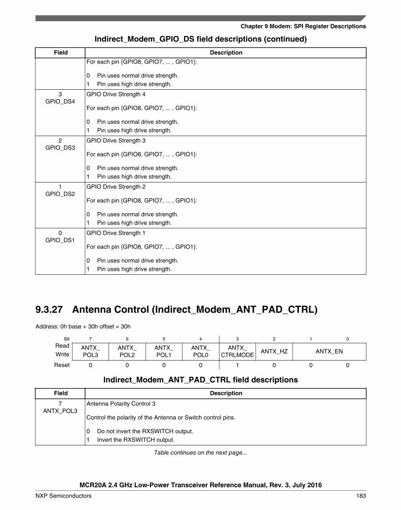
Indirect_Modem_GPIO_DS field descriptions (continued)
Field Description
For each pin {GPIO8, GPIO7, ... , GPIO1}:
0 Pin uses normal drive strength.1 Pin uses high drive strength.
3GPIO_DS4
GPIO Drive Strength 4
For each pin {GPIO8, GPIO7, ... , GPIO1}:
0 Pin uses normal drive strength.1 Pin uses high drive strength.
2GPIO_DS3
GPIO Drive Strength 3
For each pin {GPIO8, GPIO7, ... , GPIO1}:
0 Pin uses normal drive strength.1 Pin uses high drive strength.
1GPIO_DS2
GPIO Drive Strength 2
For each pin {GPIO8, GPIO7, ... , GPIO1}:
0 Pin uses normal drive strength.1 Pin uses high drive strength.
0GPIO_DS1
GPIO Drive Strength 1
For each pin {GPIO8, GPIO7, ... , GPIO1}:
0 Pin uses normal drive strength.1 Pin uses high drive strength.
9.3.27 Antenna Control (Indirect_Modem_ANT_PAD_CTRL)
Address: 0h base + 30h offset = 30h
Bit 7 6 5 4 3 2 1 0
Read ANTX_POL3
ANTX_POL2
ANTX_POL1
ANTX_POL0
ANTX_CTRLMODE
ANTX_HZ ANTX_ENWrite
Reset 0 0 0 0 1 0 0 0
Indirect_Modem_ANT_PAD_CTRL field descriptions
Field Description
7ANTX_POL3
Antenna Polarity Control 3
Control the polarity of the Antenna or Switch control pins.
0 Do not invert the RXSWITCH output.1 Invert the RXSWITCH output.
Table continues on the next page...
Chapter 9 Modem: SPI Register Descriptions
MCR20A 2.4 GHz Low-Power Transceiver Reference Manual, Rev. 3, July 2016
NXP Semiconductors 183
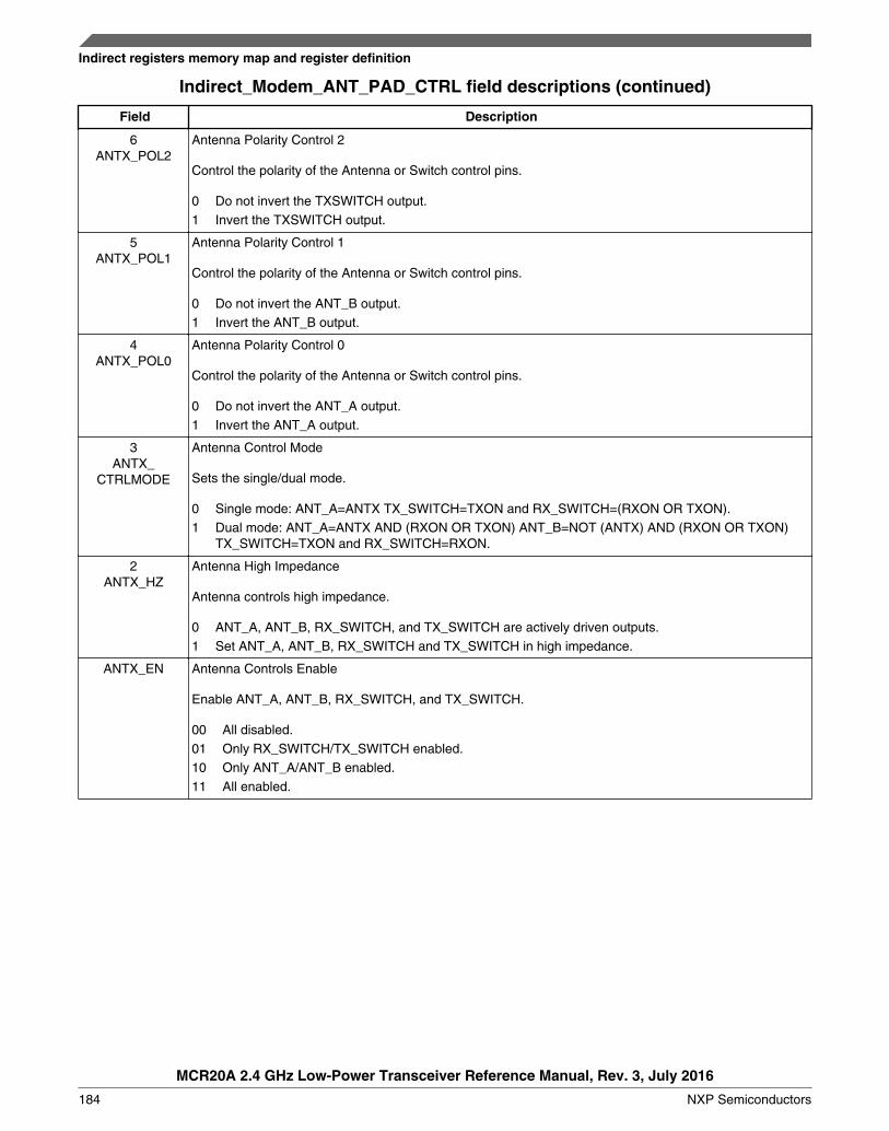
Indirect_Modem_ANT_PAD_CTRL field descriptions (continued)
Field Description
6ANTX_POL2
Antenna Polarity Control 2
Control the polarity of the Antenna or Switch control pins.
0 Do not invert the TXSWITCH output.1 Invert the TXSWITCH output.
5ANTX_POL1
Antenna Polarity Control 1
Control the polarity of the Antenna or Switch control pins.
0 Do not invert the ANT_B output.1 Invert the ANT_B output.
4ANTX_POL0
Antenna Polarity Control 0
Control the polarity of the Antenna or Switch control pins.
0 Do not invert the ANT_A output.1 Invert the ANT_A output.
3ANTX_
CTRLMODE
Antenna Control Mode
Sets the single/dual mode.
0 Single mode: ANT_A=ANTX TX_SWITCH=TXON and RX_SWITCH=(RXON OR TXON).1 Dual mode: ANT_A=ANTX AND (RXON OR TXON) ANT_B=NOT (ANTX) AND (RXON OR TXON)
TX_SWITCH=TXON and RX_SWITCH=RXON.
2ANTX_HZ
Antenna High Impedance
Antenna controls high impedance.
0 ANT_A, ANT_B, RX_SWITCH, and TX_SWITCH are actively driven outputs.1 Set ANT_A, ANT_B, RX_SWITCH and TX_SWITCH in high impedance.
ANTX_EN Antenna Controls Enable
Enable ANT_A, ANT_B, RX_SWITCH, and TX_SWITCH.
00 All disabled.01 Only RX_SWITCH/TX_SWITCH enabled.10 Only ANT_A/ANT_B enabled.11 All enabled.
Indirect registers memory map and register definition
MCR20A 2.4 GHz Low-Power Transceiver Reference Manual, Rev. 3, July 2016
184 NXP Semiconductors
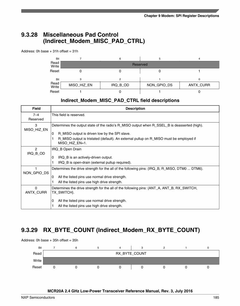
9.3.28 Miscellaneous Pad Control(Indirect_Modem_MISC_PAD_CTRL)
Address: 0h base + 31h offset = 31h
Bit 7 6 5 4
Read ReservedWriteReset 0 0 0 1
Bit 3 2 1 0
Read MISO_HIZ_EN IRQ_B_OD NON_GPIO_DS ANTX_CURRWriteReset 1 0 1 0
Indirect_Modem_MISC_PAD_CTRL field descriptions
Field Description
7–4Reserved
This field is reserved.
3MISO_HIZ_EN
Determines the output state of the radio’s R_MISO output when R_SSEL_B is deasserted (high).
0 R_MISO output is driven low by the SPI slave.1 R_MISO output is tristated (default). An external pullup on R_MISO must be employed if
MISO_HIZ_EN=1.
2IRQ_B_OD
IRQ_B Open Drain
0 IRQ_B is an actively-driven output.1 IRQ_B is open-drain (external pullup required).
1NON_GPIO_DS
Determines the drive strength for the all of the following pins: {IRQ_B, R_MISO, DTM0 ... DTM6}.
0 All the listed pins use normal drive strength.1 All the listed pins use high drive strength.
0ANTX_CURR
Determines the drive strength for the all of the following pins: {ANT_A, ANT_B, RX_SWITCH,TX_SWITCH}.
0 All the listed pins use normal drive strength.1 All the listed pins use high drive strength.
9.3.29 RX_BYTE_COUNT (Indirect_Modem_RX_BYTE_COUNT)
Address: 0h base + 35h offset = 35h
Bit 7 6 5 4 3 2 1 0
Read RX_BYTE_COUNT
Write
Reset 0 0 0 0 0 0 0 0
Chapter 9 Modem: SPI Register Descriptions
MCR20A 2.4 GHz Low-Power Transceiver Reference Manual, Rev. 3, July 2016
NXP Semiconductors 185
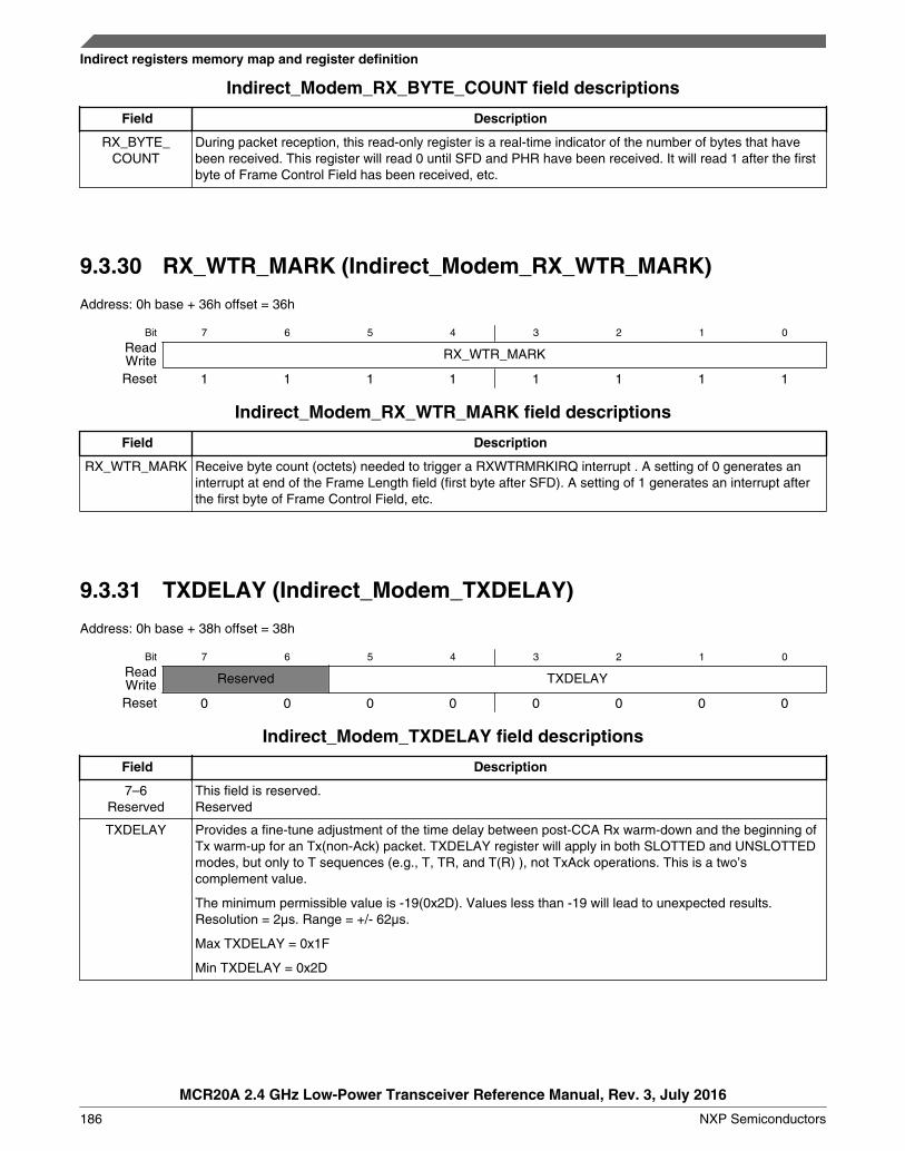
Indirect_Modem_RX_BYTE_COUNT field descriptions
Field Description
RX_BYTE_COUNT
During packet reception, this read-only register is a real-time indicator of the number of bytes that havebeen received. This register will read 0 until SFD and PHR have been received. It will read 1 after the firstbyte of Frame Control Field has been received, etc.
9.3.30 RX_WTR_MARK (Indirect_Modem_RX_WTR_MARK)
Address: 0h base + 36h offset = 36h
Bit 7 6 5 4 3 2 1 0
Read RX_WTR_MARKWriteReset 1 1 1 1 1 1 1 1
Indirect_Modem_RX_WTR_MARK field descriptions
Field Description
RX_WTR_MARK Receive byte count (octets) needed to trigger a RXWTRMRKIRQ interrupt . A setting of 0 generates aninterrupt at end of the Frame Length field (first byte after SFD). A setting of 1 generates an interrupt afterthe first byte of Frame Control Field, etc.
9.3.31 TXDELAY (Indirect_Modem_TXDELAY)
Address: 0h base + 38h offset = 38h
Bit 7 6 5 4 3 2 1 0
Read Reserved TXDELAYWriteReset 0 0 0 0 0 0 0 0
Indirect_Modem_TXDELAY field descriptions
Field Description
7–6Reserved
This field is reserved.Reserved
TXDELAY Provides a fine-tune adjustment of the time delay between post-CCA Rx warm-down and the beginning ofTx warm-up for an Tx(non-Ack) packet. TXDELAY register will apply in both SLOTTED and UNSLOTTEDmodes, but only to T sequences (e.g., T, TR, and T(R) ), not TxAck operations. This is a two’scomplement value.
The minimum permissible value is -19(0x2D). Values less than -19 will lead to unexpected results.Resolution = 2μs. Range = +/- 62μs.
Max TXDELAY = 0x1F
Min TXDELAY = 0x2D
Indirect registers memory map and register definition
MCR20A 2.4 GHz Low-Power Transceiver Reference Manual, Rev. 3, July 2016
186 NXP Semiconductors
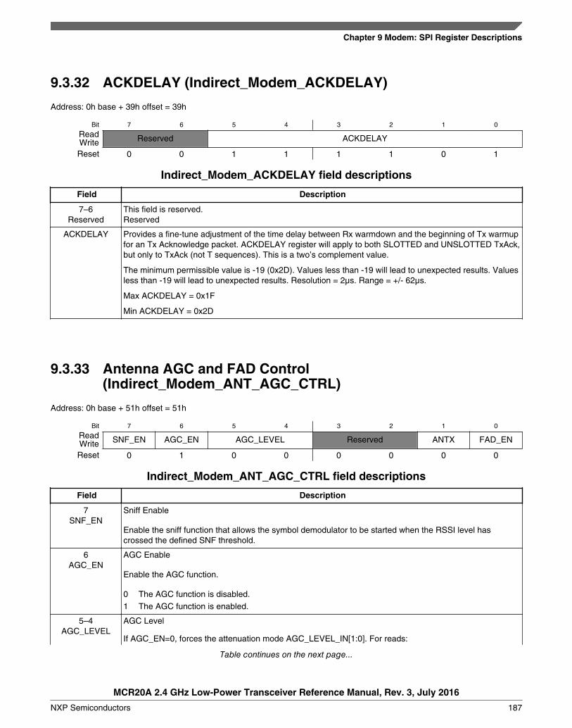
9.3.32 ACKDELAY (Indirect_Modem_ACKDELAY)
Address: 0h base + 39h offset = 39h
Bit 7 6 5 4 3 2 1 0
Read Reserved ACKDELAYWriteReset 0 0 1 1 1 1 0 1
Indirect_Modem_ACKDELAY field descriptions
Field Description
7–6Reserved
This field is reserved.Reserved
ACKDELAY Provides a fine-tune adjustment of the time delay between Rx warmdown and the beginning of Tx warmupfor an Tx Acknowledge packet. ACKDELAY register will apply to both SLOTTED and UNSLOTTED TxAck,but only to TxAck (not T sequences). This is a two’s complement value.
The minimum permissible value is -19 (0x2D). Values less than -19 will lead to unexpected results. Valuesless than -19 will lead to unexpected results. Resolution = 2μs. Range = +/- 62μs.
Max ACKDELAY = 0x1F
Min ACKDELAY = 0x2D
9.3.33 Antenna AGC and FAD Control(Indirect_Modem_ANT_AGC_CTRL)
Address: 0h base + 51h offset = 51h
Bit 7 6 5 4 3 2 1 0
Read SNF_EN AGC_EN AGC_LEVEL Reserved ANTX FAD_ENWriteReset 0 1 0 0 0 0 0 0
Indirect_Modem_ANT_AGC_CTRL field descriptions
Field Description
7SNF_EN
Sniff Enable
Enable the sniff function that allows the symbol demodulator to be started when the RSSI level hascrossed the defined SNF threshold.
6AGC_EN
AGC Enable
Enable the AGC function.
0 The AGC function is disabled.1 The AGC function is enabled.
5–4AGC_LEVEL
AGC Level
If AGC_EN=0, forces the attenuation mode AGC_LEVEL_IN[1:0]. For reads:
Table continues on the next page...
Chapter 9 Modem: SPI Register Descriptions
MCR20A 2.4 GHz Low-Power Transceiver Reference Manual, Rev. 3, July 2016
NXP Semiconductors 187
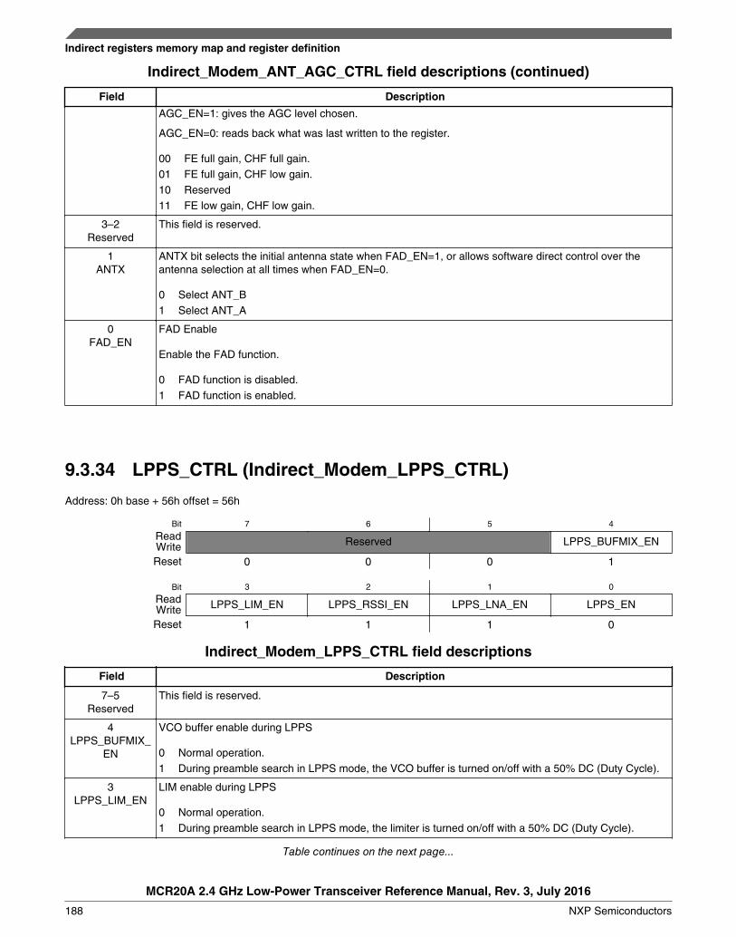
Indirect_Modem_ANT_AGC_CTRL field descriptions (continued)
Field Description
AGC_EN=1: gives the AGC level chosen.
AGC_EN=0: reads back what was last written to the register.
00 FE full gain, CHF full gain.01 FE full gain, CHF low gain.10 Reserved11 FE low gain, CHF low gain.
3–2Reserved
This field is reserved.
1ANTX
ANTX bit selects the initial antenna state when FAD_EN=1, or allows software direct control over theantenna selection at all times when FAD_EN=0.
0 Select ANT_B1 Select ANT_A
0FAD_EN
FAD Enable
Enable the FAD function.
0 FAD function is disabled.1 FAD function is enabled.
9.3.34 LPPS_CTRL (Indirect_Modem_LPPS_CTRL)
Address: 0h base + 56h offset = 56h
Bit 7 6 5 4
Read Reserved LPPS_BUFMIX_ENWriteReset 0 0 0 1
Bit 3 2 1 0
Read LPPS_LIM_EN LPPS_RSSI_EN LPPS_LNA_EN LPPS_ENWriteReset 1 1 1 0
Indirect_Modem_LPPS_CTRL field descriptions
Field Description
7–5Reserved
This field is reserved.
4LPPS_BUFMIX_
EN
VCO buffer enable during LPPS
0 Normal operation.1 During preamble search in LPPS mode, the VCO buffer is turned on/off with a 50% DC (Duty Cycle).
3LPPS_LIM_EN
LIM enable during LPPS
0 Normal operation.1 During preamble search in LPPS mode, the limiter is turned on/off with a 50% DC (Duty Cycle).
Table continues on the next page...
Indirect registers memory map and register definition
MCR20A 2.4 GHz Low-Power Transceiver Reference Manual, Rev. 3, July 2016
188 NXP Semiconductors
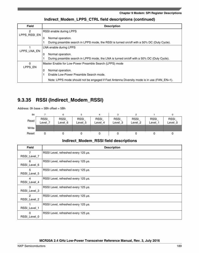
Indirect_Modem_LPPS_CTRL field descriptions (continued)
Field Description
2LPPS_RSSI_EN
RSSI enable during LPPS
0 Normal operation.1 During preamble search in LPPS mode, the RSSI is turned on/off with a 50% DC (Duty Cycle).
1LPPS_LNA_EN
LNA enable during LPPS
0 Normal operation.1 During preamble search in LPPS mode, the LNA is turned on/off with a 50% DC (Duty Cycle).
0LPPS_EN
Master Enable for Low-Power Preamble Search (LPPS) mode
0 Normal operation.1 Enable Low-Power Preamble Search mode.
Note: LPPS mode should not be engaged if Fast Antenna Diversity mode is in use (FAN_EN=1).
9.3.35 RSSI (Indirect_Modem_RSSI)
Address: 0h base + 5Bh offset = 5Bh
Bit 7 6 5 4 3 2 1 0
ReadRSSI_
Level_7RSSI_
Level_6RSSI_
Level_5RSSI_
Level_4RSSI_
Level_3RSSI_
Level_2RSSI_
Level_1RSSI_
Level_0
Write
Reset 0 0 0 0 0 0 0 0
Indirect_Modem_RSSI field descriptions
Field Description
7RSSI_Level_7
RSSI Level, refreshed every 125 µs.
6RSSI_Level_6
RSSI Level, refreshed every 125 µs.
5RSSI_Level_5
RSSI Level, refreshed every 125 µs.
4RSSI_Level_4
RSSI Level, refreshed every 125 µs.
3RSSI_Level_3
RSSI Level, refreshed every 125 µs.
2RSSI_Level_2
RSSI Level, refreshed every 125 µs.
1RSSI_Level_1
RSSI Level, refreshed every 125 µs.
0RSSI_Level_0
RSSI Level, refreshed every 125 µs.
Chapter 9 Modem: SPI Register Descriptions
MCR20A 2.4 GHz Low-Power Transceiver Reference Manual, Rev. 3, July 2016
NXP Semiconductors 189
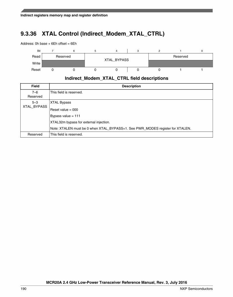
9.3.36 XTAL Control (Indirect_Modem_XTAL_CTRL)
Address: 0h base + 6Eh offset = 6Eh
Bit 7 6 5 4 3 2 1 0
Read ReservedXTAL_BYPASS
Reserved
Write
Reset 0 0 0 0 0 0 1 1
Indirect_Modem_XTAL_CTRL field descriptions
Field Description
7–6Reserved
This field is reserved.
5–3XTAL_BYPASS
XTAL Bypass
Reset value = 000
Bypass value = 111
XTAL32m bypass for external injection.
Note: XTALEN must be 0 when XTAL_BYPASS=1. See PWR_MODES register for XTALEN.
Reserved This field is reserved.
Indirect registers memory map and register definition
MCR20A 2.4 GHz Low-Power Transceiver Reference Manual, Rev. 3, July 2016
190 NXP Semiconductors

Appendix ARelease Notes for Revision 3
A.1 General changes throughout
• Updated missing reset values of Modem and Indirect Modem registers.• Added the following registers to the Indirect Modem memory map: TMR_PRESCALE, RX_BYTE_COUNT,
RX_WTR_MARK, TXDELAY, ACKDELAY.• Updated register bit map structure of XTAL Control (Indirect Modem_XTAL_CTRL) register.
MCR20A 2.4 GHz Low-Power Transceiver Reference Manual, Rev. 3, July 2016
NXP Semiconductors 191

MCR20A 2.4 GHz Low-Power Transceiver Reference Manual, Rev. 3, July 2016
192 NXP Semiconductors

How to Reach Us:
Home Page:nxp.com
Web Support:nxp.com/support
Information in this document is provided solely to enable system and softwareimplementers to use NXP products. There are no express or implied copyrightlicenses granted hereunder to design or fabricate any integrated circuits basedon the information in this document. NXP reserves the right to make changeswithout further notice to any products herein.
NXP makes no warranty, representation, or guarantee regarding the suitability ofits products for any particular purpose, nor does NXP assume any liability arisingout of the application or use of any product or circuit, and specifically disclaimsany and all liability, including without limitation consequential or incidentaldamages. “Typical” parameters that may be provided in NXP data sheets and/orspecifications can and do vary in different applications, and actual performancemay vary over time. All operating parameters, including “typicals,” must bevalidated for each customer application by customer's technical experts. NXPdoes not convey any license under its patent rights nor the rights of others. NXPsells products pursuant to standard terms and conditions of sale, which can befound at the following address: nxp.com/SalesTermsandConditions.
NXP, the NXP logo, NXP SECURE CONNECTIONS FOR A SMARTERWORLD, Freescale, the Freescale logo, and Kinetis are trademarks of NXP B.V.All other product or service names are the property of their respective owners. Allrights reserved.
© 2013 – 2016 NXP B.V.
Document Number MCR20ARMRevision 3, July 2016