buck boost) using linkswitchtm-pl lnk458kg · pdf file08-jun-11 4.5 w buck boost power supply...
TRANSCRIPT

Power Integrations
5245 Hellyer Avenue, San Jose, CA 95138 USA. Tel: +1 408 414 9200 Fax: +1 408 414 9201
www.powerint.com
Title
Reference Design Report for 4.5 W Power Factor Corrected LED Driver (Non-Isolated Buck Boost) Using LinkSwitchTM-PL LNK458KG
Specification 85 VAC – 135 VAC Input; 35 V, 130 mA Output
Application LED Driver for E17 Lamp Replacement
Author Applications Engineering Department
Document Number
RDR-271
Date June 8, 2011
Revision 1.0 Summary and Features Single-stage power factor corrected and accurate constant current (CC) output Low cost, low component count and small PCB footprint solution Highly energy efficient, >85 % at 115 VAC input Superior performance and end user experience Fast start-up time (<300 ms) – no perceptible delay Integrated protection and reliability features
Single shot no-load protection / output short-circuit protected with auto-recovery Auto-recovering thermal shutdown with large hysteresis protects both components and PCB No damage during brown-out conditions
PF >0.95 at 115 VAC Meets EN55015 conducted EMI %A THD <15% at 115 VAC Meets IEC ring wave, differential line surge and EN55015 conducted EMI No potting required up to 90 ºC internal ambient PATENT INFORMATION The products and applications illustrated herein (including transformer construction and circuits external to the products) may be covered by one or more U.S. and foreign patents, or potentially by pending U.S. and foreign patent applications assigned to Power Integrations. A complete list of Power Integrations' patents may be found at www.powerint.com. Power Integrations grants its customers a license under certain patent rights as set forth at <http://www.powerint.com/ip.htm>.

RDR-271 4.5 W Buck Boost Power Supply Using LNK458KG 08-Jun-11
Page 2 of 47
Power Integrations, Inc. Tel: +1 408 414 9200 Fax: +1 408 414 9201 www.powerint.com
Table of Contents 1 Introduction ................................................................................................................. 4 2 Power Supply Specification ........................................................................................ 7 3 Schematic ................................................................................................................... 8 4 Circuit Description ...................................................................................................... 9
4.1 Input EMI Filtering ............................................................................................... 9 4.2 Buck Boost using LinkSwitch-PL ......................................................................... 9 4.3 Output Feedback ............................................................................................... 10 4.4 Disconnected Load Protection ........................................................................... 10 4.5 Reference Design Kit ........................................................................................ 10
5 PCB Layout .............................................................................................................. 12 6 Bill of Materials ......................................................................................................... 15
6.1 Lamp Bill of Materials ........................................................................................ 15 6.2 LED Load Bill of Materials ................................................................................. 15
7 Inductor Specification ............................................................................................... 16 7.1 Electrical Diagram ............................................................................................. 16 7.2 Electrical Specifications ..................................................................................... 16 7.3 Materials ............................................................................................................ 16 7.4 Inductor Build Diagram ...................................................................................... 17 7.5 Inductor Construction ........................................................................................ 17
8 Inductor Illustration ................................................................................................... 18 9 Inductor Design Spreadsheet ................................................................................... 21 10 Performance Data ................................................................................................. 23
10.1 Active Mode Efficiency ...................................................................................... 23 10.2 Line Regulation ................................................................................................. 24 10.3 Power Factor ..................................................................................................... 25 10.4 %THD ................................................................................................................ 26 10.5 Harmonic Measurements .................................................................................. 27
11 Thermal Performance ........................................................................................... 29 11.1 Equipment Used ................................................................................................ 29 11.2 Thermal Results ................................................................................................ 30
12 Thermal Scans ...................................................................................................... 31 13 Waveforms ............................................................................................................ 32
13.1 Drain Voltage and Current, Normal Operation ................................................... 32 13.2 Drain Voltage and Current Start-up Profile ........................................................ 33 13.3 Output Voltage Start-up Profile .......................................................................... 35 13.4 Drain Voltage and Current Start-up Short Profile .............................................. 36 13.5 Line Transient Response ................................................................................... 37 13.6 Brown-out .......................................................................................................... 39 13.7 Start-up No-load ................................................................................................ 40 13.8 Line Surge Waveform ........................................................................................ 41
14 Line Surge ............................................................................................................. 42 15 Conducted EMI ..................................................................................................... 43
15.1 Equipment: ........................................................................................................ 43 15.2 EMI Test Set-up ................................................................................................ 43
08-Jun-11 4.5 W Buck Boost Power Supply Using LNK458KG
Page 3 of 47
Power Integrations Tel: +1 408 414 9200 Fax: +1 408 414 9201
www.powerint.com
16 Revision History .................................................................................................... 46 Important Note: Although this board is designed to satisfy safety requirements for non-isolated LED driver, the engineering prototype has not been agency approved. Therefore, all testing should be performed using an isolation transformer to provide the AC input to the prototype board.
RDR-271 4.5 W Buck Boost Power Supply Using LNK458KG 08-Jun-11
Page 4 of 47
Power Integrations, Inc. Tel: +1 408 414 9200 Fax: +1 408 414 9201 www.powerint.com
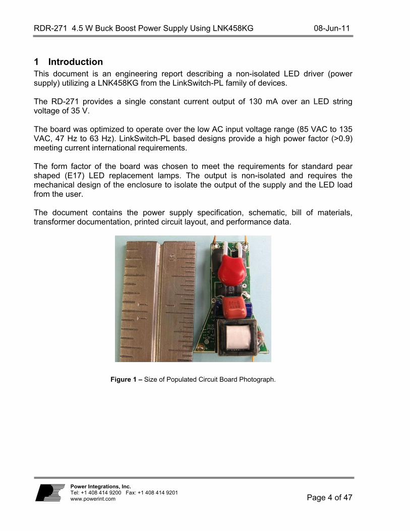
1 Introduction This document is an engineering report describing a non-isolated LED driver (power supply) utilizing a LNK458KG from the LinkSwitch-PL family of devices. The RD-271 provides a single constant current output of 130 mA over an LED string voltage of 35 V. The board was optimized to operate over the low AC input voltage range (85 VAC to 135 VAC, 47 Hz to 63 Hz). LinkSwitch-PL based designs provide a high power factor (>0.9) meeting current international requirements. The form factor of the board was chosen to meet the requirements for standard pear shaped (E17) LED replacement lamps. The output is non-isolated and requires the mechanical design of the enclosure to isolate the output of the supply and the LED load from the user. The document contains the power supply specification, schematic, bill of materials, transformer documentation, printed circuit layout, and performance data.
Figure 1 – Size of Populated Circuit Board Photograph.
08-Jun-11 4.5 W Buck Boost Power Supply Using LNK458KG
Page 5 of 47
Power Integrations Tel: +1 408 414 9200 Fax: +1 408 414 9201
www.powerint.com
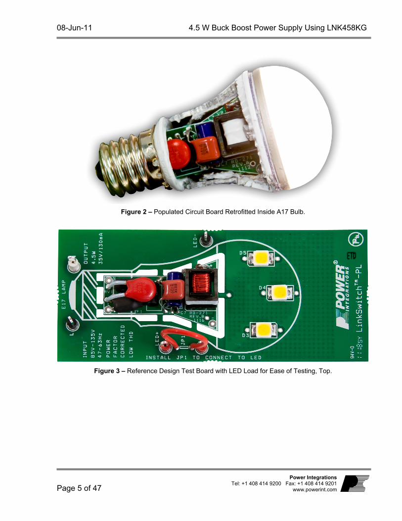
Figure 2 – Populated Circuit Board Retrofitted Inside A17 Bulb.
Figure 3 – Reference Design Test Board with LED Load for Ease of Testing, Top.
RDR-271 4.5 W Buck Boost Power Supply Using LNK458KG 08-Jun-11
Page 6 of 47
Power Integrations, Inc. Tel: +1 408 414 9200 Fax: +1 408 414 9201 www.powerint.com
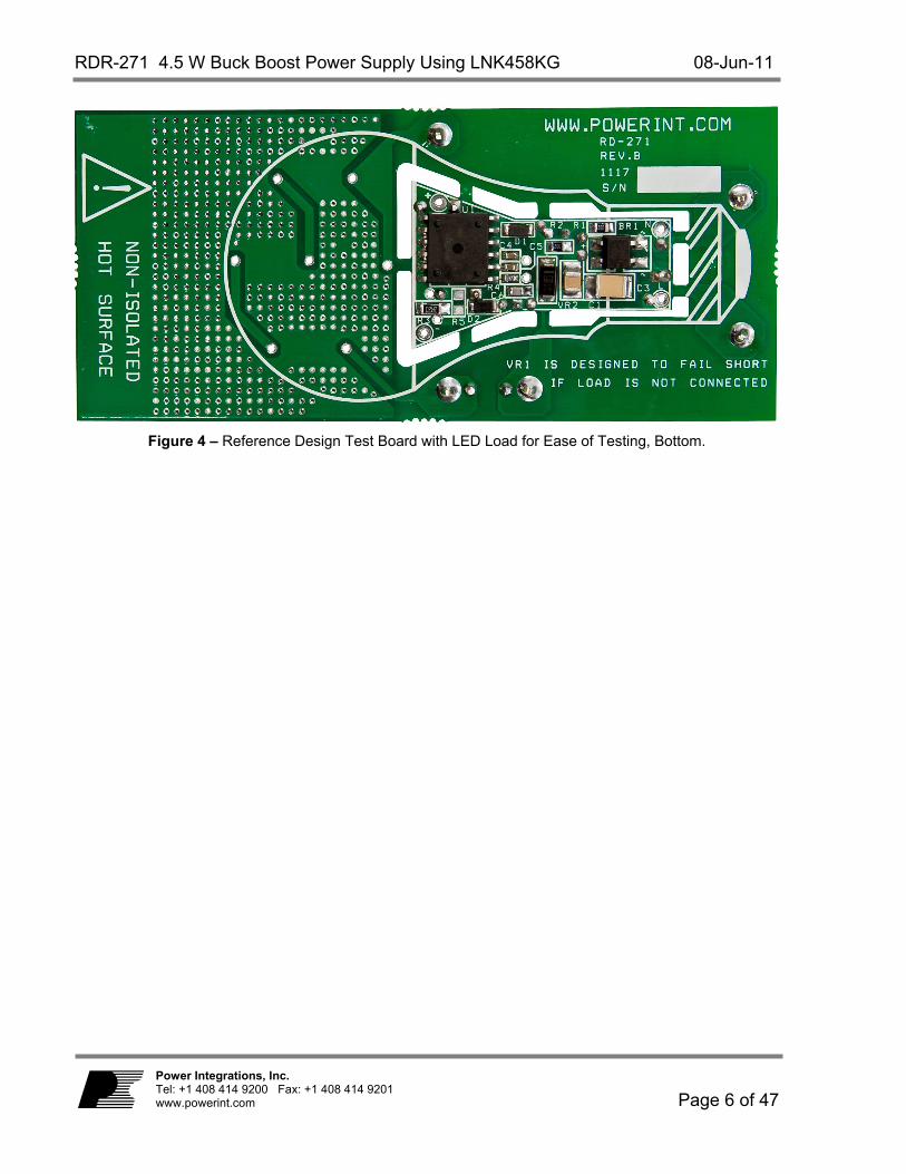
Figure 4 – Reference Design Test Board with LED Load for Ease of Testing, Bottom.
08-Jun-11 4.5 W Buck Boost Power Supply Using LNK458KG
Page 7 of 47
Power Integrations Tel: +1 408 414 9200 Fax: +1 408 414 9201
www.powerint.com
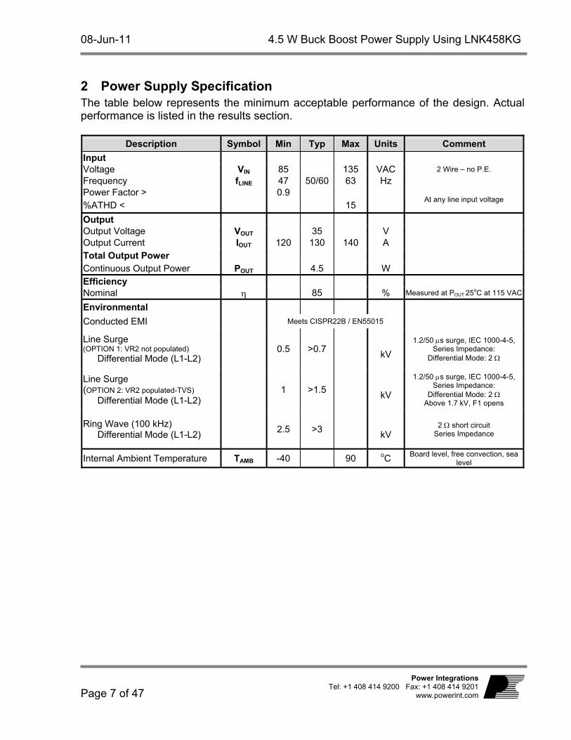
2 Power Supply Specification The table below represents the minimum acceptable performance of the design. Actual performance is listed in the results section.
Description Symbol Min Typ Max Units Comment
Input Voltage VIN 85 135 VAC 2 Wire – no P.E.
Frequency fLINE 47 50/60 63 Hz
Power Factor > 0.9 At any line input voltage
%ATHD < 15
Output
Output Voltage VOUT 35 V
Output Current IOUT 120 130 140 A
Total Output Power
Continuous Output Power POUT 4.5 W
Efficiency
Nominal 85 % Measured at POUT 25oC at 115 VAC
Environmental
Conducted EMI Meets CISPR22B / EN55015
Line Surge (OPTION 1: VR2 not populated)
Differential Mode (L1-L2) 0.5 >0.7
kV
1.2/50 s surge, IEC 1000-4-5, Series Impedance:
Differential Mode: 2
Line Surge (OPTION 2: VR2 populated-TVS)
Differential Mode (L1-L2) 1 >1.5
kV
1.2/50 s surge, IEC 1000-4-5, Series Impedance:
Differential Mode: 2 Above 1.7 kV, F1 opens
Ring Wave (100 kHz) Differential Mode (L1-L2)
2.5 >3
kV 2 short circuit
Series Impedance
Internal Ambient Temperature TAMB -40 90 oC Board level, free convection, sea level
RDR-271 4.5 W Buck Boost Power Supply Using LNK458KG 08-Jun-11
Page 8 of 47
Power Integrations, Inc. Tel: +1 408 414 9200 Fax: +1 408 414 9201 www.powerint.com
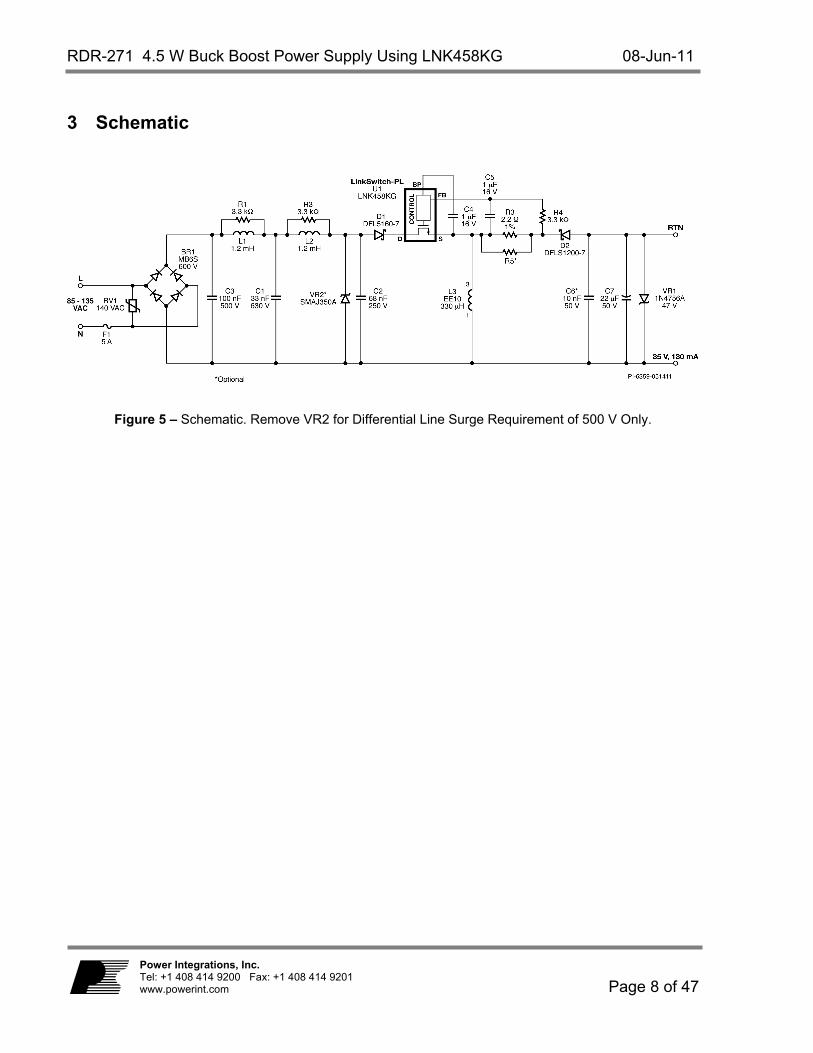
3 Schematic
Figure 5 – Schematic. Remove VR2 for Differential Line Surge Requirement of 500 V Only.
08-Jun-11 4.5 W Buck Boost Power Supply Using LNK458KG
Page 9 of 47
Power Integrations Tel: +1 408 414 9200 Fax: +1 408 414 9201
www.powerint.com
4 Circuit Description The LinkSwitch-PL (U1) is a highly integrated primary side controller intended for use in LED driver applications. The LinkSwitch-PL provides high power factor in a single-stage conversion topology while regulating the output current in a wide range of input (85 VAC -135 VAC) and output voltage variations typical in LED driver application environment. All of the control circuitry responsible for these functions plus a high-voltage power MOSFET is incorporated into the device.
4.1 Input EMI Filtering Fuse F1 provides protection against component failure. A fast 5 A rating (this being relatively high) was needed to prevent false opening during line surges. The maximum input voltage is clamped by RV1 and by VR2 (TVS) during differential line surges. Zener diode VR2 can be removed for a differential line surge requirement of ≤500 V. The AC input is full wave rectified by BR1 (vs. half wave) to achieve good power factor and THD. Capacitor C1, C2, C3 and differential choke L1 and L2 perform EMI filtering while the limited total capacitance maintains high power factor. This input 2- filter network plus the frequency jittering feature of LinkSwitch-PL allows compliance to Class B emission limits. Resistor R1 and R2 were used to damp the resonance of the EMI filter, preventing peaks in the EMI spectrum.
Inductor L1 and L2 are positioned after the bridge to avoid an imbalance in the EMI scan between line and neutral. This gives also leeway to use small high-voltage ceramic capacitors in the input filter.
Capacitor C2 is a film capacitor to achieve more than 10 dBV design margin. It may be replaced by X7R high-voltage ceramic capacitor if EMI design margin requirement is relaxed (<4 dBV margin)
4.2 Buck Boost using LinkSwitch-PL The buck boost power train is composed of U1 (power switch + control), D2 (free-wheeling diode), C6 and C7 (output capacitor), and L3 (inductor). Diode D1 was used to prevent negative voltage appearing across the drain-source of U1 especially near the zero-crossing of the input voltage. The bypass capacitor C4 provides the internal supply for the device when the power MOSFET is on.
Diode D1 and D2 are low drop diodes (Schottky) to maximize efficiency. Inductor L3 winding construction and wire gauge are optimized to minimize inter-
winding capacitance and reduces AC losses.
RDR-271 4.5 W Buck Boost Power Supply Using LNK458KG 08-Jun-11
Page 10 of 47
Power Integrations, Inc. Tel: +1 408 414 9200 Fax: +1 408 414 9201 www.powerint.com
4.3 Output Feedback The output current feedback is sensed on the voltage drop across R3 and then filtered by a low pass filter, R4 and C5, to keep the LinkSwitch-PL operating point such that the average FEEDBACK (FB) pin voltage is 290 mV steady-state.
Resistor R5 is provisioned in parallel with R3 to allow centering of the output current.
4.4 Disconnected Load Protection The system is protected by VR1 if the load is not connected in order to avoid catastrophic failure of C7 (output capacitor). Zener diode VR1 will short the output it the load is not connected; this protection is not auto-recovering. Replace VR1 if this occurs in order to reuse the LED driver. Note that at the system level the LED load is always connected. If the system will be potted or enclosed tightly, VR1 might not be required. Replace VR1 with an SCR clamp circuit it auto-recovery is required.
4.5 Reference Design Kit The reference design is mounted with LED load as a complete kit. The load is for illustration and can be operated at 25 ºC ambient maximum only. A loop wire can be used for monitoring the output current via current probe or clamp. The board can be dismantled to fit to common E17 lamps and for higher operating temperature test condition.
Want More?Use your smartphone and free software from www.neoreader.com (or any other free QR Code Reader from your smartphone’s App Store) and you will be connected to related content

08-Jun-11 4.5 W Buck Boost Power Supply Using LNK458KG
Page 11 of 47
Power Integrations Tel: +1 408 414 9200 Fax: +1 408 414 9201
www.powerint.com

RDR-271 4.5 W Buck Boost Power Supply Using LNK458KG 08-Jun-11
Page 12 of 47
Power Integrations, Inc. Tel: +1 408 414 9200 Fax: +1 408 414 9201 www.powerint.com
5 PCB Layout
Figure 6 – Top Printed Circuit Layout.
Figure 7 – Bottom Printed Circuit Layout.
08-Jun-11 4.5 W Buck Boost Power Supply Using LNK458KG
Page 13 of 47
Power Integrations Tel: +1 408 414 9200 Fax: +1 408 414 9201
www.powerint.com
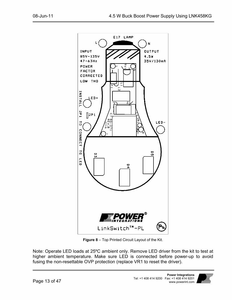
Figure 8 – Top Printed Circuit Layout of the Kit.
Note: Operate LED loads at 25ºC ambient only. Remove LED driver from the kit to test at higher ambient temperature. Make sure LED is connected before power-up to avoid fusing the non-resettable OVP protection (replace VR1 to reset the driver).
RDR-271 4.5 W Buck Boost Power Supply Using LNK458KG 08-Jun-11
Page 14 of 47
Power Integrations, Inc. Tel: +1 408 414 9200 Fax: +1 408 414 9201 www.powerint.com
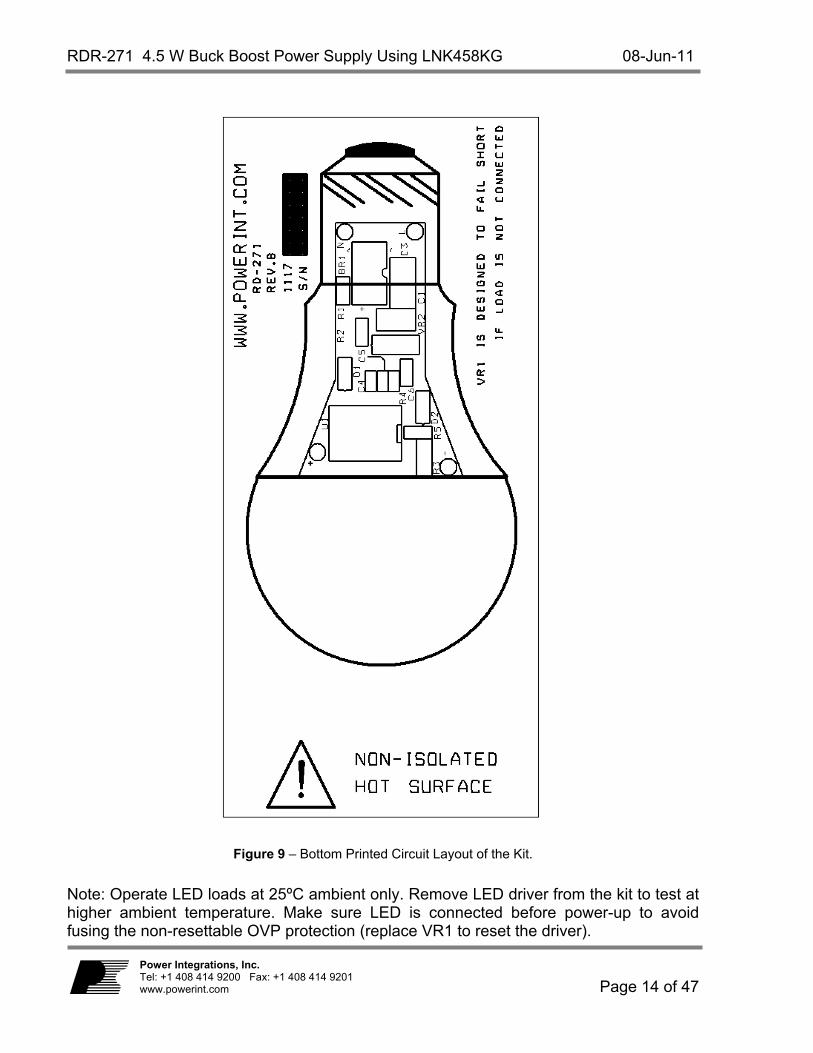
Figure 9 – Bottom Printed Circuit Layout of the Kit.
Note: Operate LED loads at 25ºC ambient only. Remove LED driver from the kit to test at higher ambient temperature. Make sure LED is connected before power-up to avoid fusing the non-resettable OVP protection (replace VR1 to reset the driver).
08-Jun-11 4.5 W Buck Boost Power Supply Using LNK458KG
Page 15 of 47
Power Integrations Tel: +1 408 414 9200 Fax: +1 408 414 9201
www.powerint.com
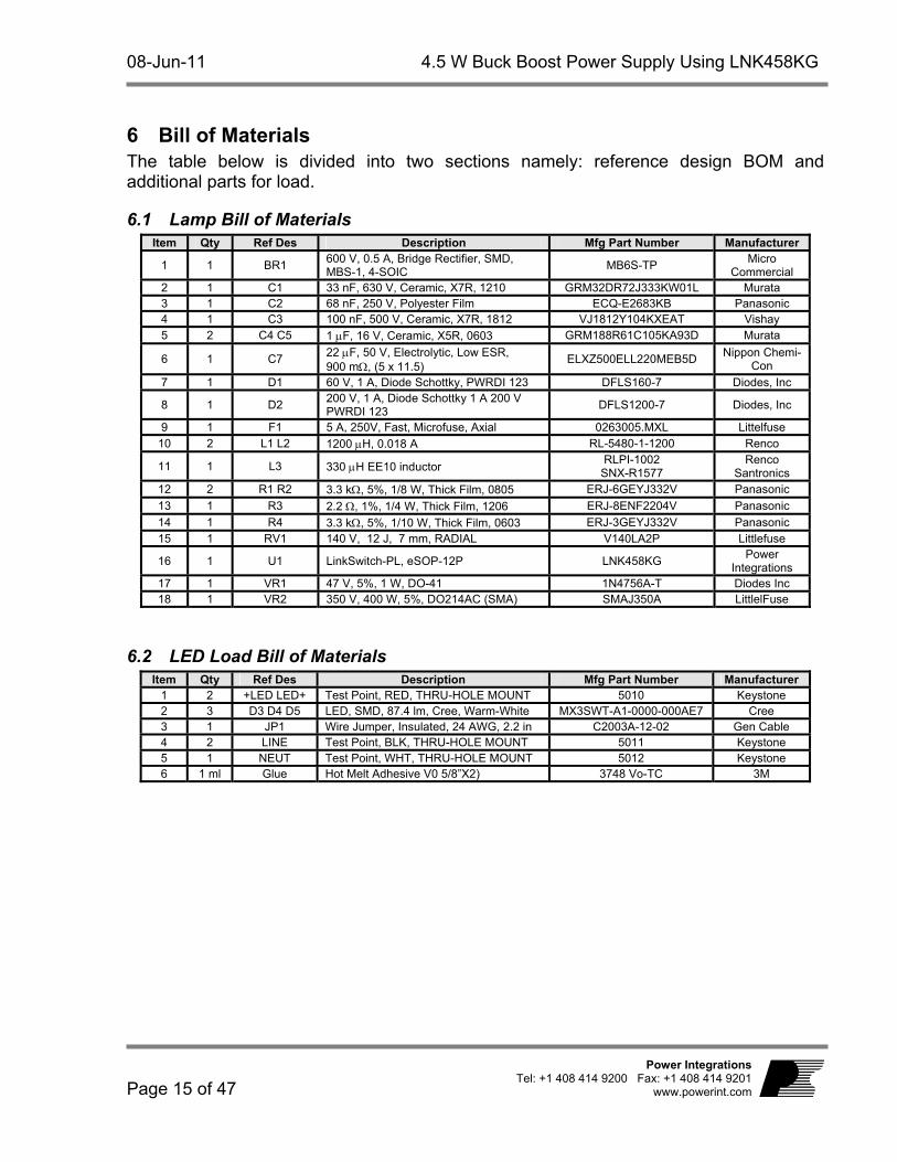
6 Bill of Materials The table below is divided into two sections namely: reference design BOM and additional parts for load.
6.1 Lamp Bill of Materials Item Qty Ref Des Description Mfg Part Number Manufacturer
1 1 BR1 600 V, 0.5 A, Bridge Rectifier, SMD, MBS-1, 4-SOIC
MB6S-TP Micro
Commercial 2 1 C1 33 nF, 630 V, Ceramic, X7R, 1210 GRM32DR72J333KW01L Murata 3 1 C2 68 nF, 250 V, Polyester Film ECQ-E2683KB Panasonic 4 1 C3 100 nF, 500 V, Ceramic, X7R, 1812 VJ1812Y104KXEAT Vishay 5 2 C4 C5 1 F, 16 V, Ceramic, X5R, 0603 GRM188R61C105KA93D Murata
6 1 C7 22 F, 50 V, Electrolytic, Low ESR, 900 m, (5 x 11.5)
ELXZ500ELL220MEB5D Nippon Chemi-
Con
7 1 D1 60 V, 1 A, Diode Schottky, PWRDI 123 DFLS160-7 Diodes, Inc
8 1 D2 200 V, 1 A, Diode Schottky 1 A 200 V PWRDI 123
DFLS1200-7 Diodes, Inc
9 1 F1 5 A, 250V, Fast, Microfuse, Axial 0263005.MXL Littelfuse 10 2 L1 L2 1200 H, 0.018 A RL-5480-1-1200 Renco
11 1 L3 330 H EE10 inductor RLPI-1002
SNX-R1577 Renco
Santronics 12 2 R1 R2 3.3 k, 5%, 1/8 W, Thick Film, 0805 ERJ-6GEYJ332V Panasonic
13 1 R3 2.2 , 1%, 1/4 W, Thick Film, 1206 ERJ-8ENF2204V Panasonic
14 1 R4 3.3 k, 5%, 1/10 W, Thick Film, 0603 ERJ-3GEYJ332V Panasonic 15 1 RV1 140 V, 12 J, 7 mm, RADIAL V140LA2P Littlefuse
16 1 U1 LinkSwitch-PL, eSOP-12P LNK458KG Power
Integrations 17 1 VR1 47 V, 5%, 1 W, DO-41 1N4756A-T Diodes Inc 18 1 VR2 350 V, 400 W, 5%, DO214AC (SMA) SMAJ350A LittlelFuse
6.2 LED Load Bill of Materials Item Qty Ref Des Description Mfg Part Number Manufacturer
1 2 +LED LED+ Test Point, RED, THRU-HOLE MOUNT 5010 Keystone 2 3 D3 D4 D5 LED, SMD, 87.4 lm, Cree, Warm-White MX3SWT-A1-0000-000AE7 Cree 3 1 JP1 Wire Jumper, Insulated, 24 AWG, 2.2 in C2003A-12-02 Gen Cable 4 2 LINE Test Point, BLK, THRU-HOLE MOUNT 5011 Keystone 5 1 NEUT Test Point, WHT, THRU-HOLE MOUNT 5012 Keystone 6 1 ml Glue Hot Melt Adhesive V0 5/8”X2) 3748 Vo-TC 3M

RDR-271 4.5 W Buck Boost Power Supply Using LNK458KG 08-Jun-11
Page 16 of 47
Power Integrations, Inc. Tel: +1 408 414 9200 Fax: +1 408 414 9201 www.powerint.com
7 Inductor Specification
7.1 Electrical Diagram
Figure 10 – Inductor Electrical Diagram.
7.2 Electrical Specifications
Primary Inductance Pins 1-3, all other windings open, measured at 100 kHz, 0.4 VRMS 330 H ±10%
7.3 Materials Item Description [1] Core: EE10/PC40
[2] Bobbin: EE10, Horizontal, 8 pins, (4/4), Taiwan Shulin Enterprise Co., Ltd. or Kunshan Fengshunhe Electronics Co., Ltd Equivalent
[3] Magnet Wire: 2 X #33 AWG [4] Loctite Super Glue Control Gel
08-Jun-11 4.5 W Buck Boost Power Supply Using LNK458KG
Page 17 of 47
Power Integrations Tel: +1 408 414 9200 Fax: +1 408 414 9201
www.powerint.com
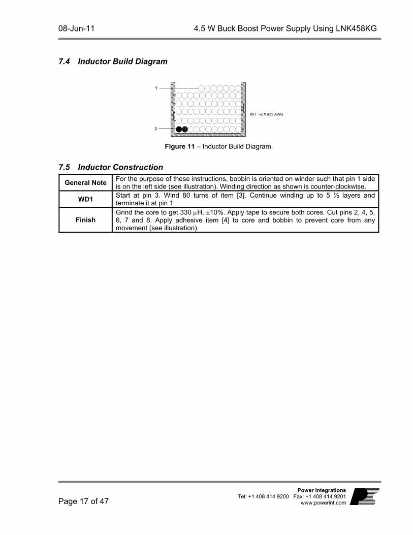
7.4 Inductor Build Diagram
3
1
80T –2 X #33 AWG
Figure 11 – Inductor Build Diagram.
7.5 Inductor Construction
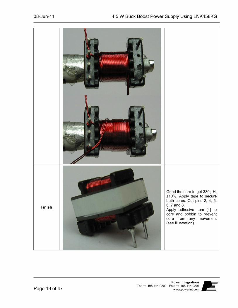
General Note For the purpose of these instructions, bobbin is oriented on winder such that pin 1 side is on the left side (see illustration). Winding direction as shown is counter-clockwise.
WD1 Start at pin 3. Wind 80 turns of item [3]. Continue winding up to 5 ½ layers and terminate it at pin 1.
Finish Grind the core to get 330 H, ±10%. Apply tape to secure both cores. Cut pins 2, 4, 5, 6, 7 and 8. Apply adhesive item [4] to core and bobbin to prevent core from any movement (see illustration).

RDR-271 4.5 W Buck Boost Power Supply Using LNK458KG 08-Jun-11
Page 18 of 47
Power Integrations, Inc. Tel: +1 408 414 9200 Fax: +1 408 414 9201 www.powerint.com
8 Inductor Illustration
Bobbin Preparation
General Note
For the purpose of these instructions, bobbin is oriented on winder such that pin 1 side is on the left side (see illustration). Winding direction as shown is counter-clockwise.
WD1
Start at pin 3. Wind 80 turns of item [3]. Continue winding up to 5 ½ layers and terminate it at pin 1.
08-Jun-11 4.5 W Buck Boost Power Supply Using LNK458KG
Page 19 of 47
Power Integrations Tel: +1 408 414 9200 Fax: +1 408 414 9201
www.powerint.com
Finish
Grind the core to get 330 H, ±10%. Apply tape to secure both cores. Cut pins 2, 4, 5, 6, 7 and 8. Apply adhesive item [4] to core and bobbin to prevent core from any movement (see illustration).
RDR-271 4.5 W Buck Boost Power Supply Using LNK458KG 08-Jun-11
Page 20 of 47
Power Integrations, Inc. Tel: +1 408 414 9200 Fax: +1 408 414 9201 www.powerint.com
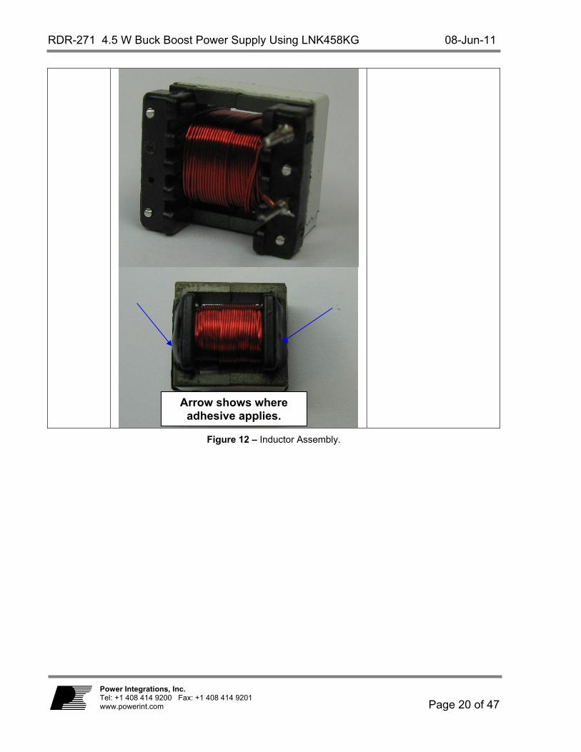
Figure 12 – Inductor Assembly.
Arrow shows where adhesive applies.

08-Jun-11 4.5 W Buck Boost Power Supply Using LNK458KG
Page 21 of 47
Power Integrations Tel: +1 408 414 9200 Fax: +1 408 414 9201
www.powerint.com
9 Inductor Design Spreadsheet Power Supply INFO OUTPUT UNIT LinkSwitch-PL Buck-boost Inductor Design Spreadsheet
VACMIN 85 85 V Minimum AC input voltage
VACNOM 115 115 V Nominal AC input voltage
VACMAX 132 132 V Maximum AC input voltage
FL 60 60 Hz Minimum line frequency
VO_MIN 30.00 30.0 V Minimum output voltage tolerance
VO_NOM 35.00 35.00 V Nominal Output Voltage
VO_MAX 38.00 38.00 V Maximum output voltage tolerance
IO 0.130 0.130 A Average output current specification
n 0.85 0.850 %/100 Total power supply efficiency
Z 0.5 Loss allocation factor
Enclosure Open Frame
Open Frame
Enclosure selections determines thermal conditions and maximum power
PO 4.55 W Total output power
VD 0.40 0.4 V Output diode forward voltage drop
LinkSwitch-PL DESIGN VARIABLES
Device LNK458 LNK458 Chosen LinkSwitch-PL Device
TON 1.67 us Expected on-time of MOSFET at low line and PO
FSW 88.9 kHz Expected switching frequency at low line and PO
Duty Cycle 14.8 % Expected operating duty cycle at low line and PO
VDRAIN 245 V Estimated worst case drain voltage at VACMAX and VO_MAX
IRMS 0.129 A Nominal RMS current through the switch
IPK 0.938 A Worst Case Peak current
ILIM_MIN 1.012 A Minimum device current limit
KDP 1.25 1.25 Ratio between off-time of switch and reset time of core at VACNOM
Device LNK458 LNK458 Chosen LinkSwitch-PL Device
LinkSwitch-PL EXTERNAL COMPONENT CALCULATIONS
RSENSE 2.231 Ohms Output current sense resistor
Standard RSENSE
2.21 Ohms Closest 1% value for RSENSE
PSENSE 37.7 mW Power dissipated by RSENSE
ENTER TRANSFORMER CORE/CONSTRUCTION VARIABLES
Core Type EE10 EE10 Core Type
Core Part Number
Custom Core Part Number (if Available)
Bobbin Part Number
Custom Bobbin Part Number (if available)
AE 12.10 12.10 mm^2 Core Effective Cross Sectional Area
LE 26.10 26.10 mm Core Effective Path Length
AL 850 850 nH/T^2 Ungapped Core Effective Inductance
BW 6.00 6 mm Bobbin Physical Winding Width
L 5 5 Number of winding layers
TRANSFORMER PRIMARY DESIGN PARAMETERS
LP 330.7 uH Primary Inductance
LP Tolerance 5.00 5 % Tolerance of Primary Inductance
N 80 80 Turns Number of Turns
RDR-271 4.5 W Buck Boost Power Supply Using LNK458KG 08-Jun-11
Page 22 of 47
Power Integrations, Inc. Tel: +1 408 414 9200 Fax: +1 408 414 9201 www.powerint.com
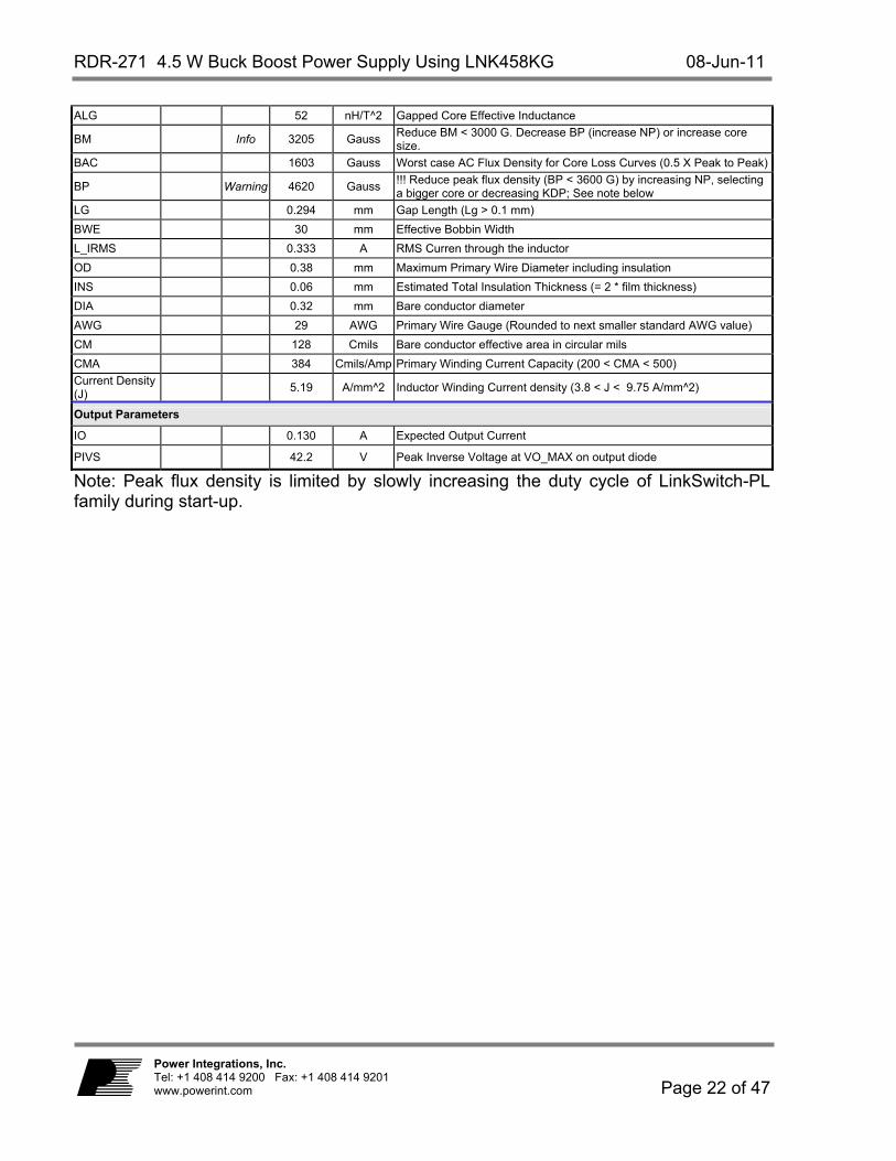
ALG 52 nH/T^2 Gapped Core Effective Inductance
BM Info 3205 Gauss Reduce BM < 3000 G. Decrease BP (increase NP) or increase core size.
BAC 1603 Gauss Worst case AC Flux Density for Core Loss Curves (0.5 X Peak to Peak)
BP Warning 4620 Gauss !!! Reduce peak flux density (BP < 3600 G) by increasing NP, selecting a bigger core or decreasing KDP; See note below
LG 0.294 mm Gap Length (Lg > 0.1 mm)
BWE 30 mm Effective Bobbin Width
L_IRMS 0.333 A RMS Curren through the inductor
OD 0.38 mm Maximum Primary Wire Diameter including insulation
INS 0.06 mm Estimated Total Insulation Thickness (= 2 * film thickness)
DIA 0.32 mm Bare conductor diameter
AWG 29 AWG Primary Wire Gauge (Rounded to next smaller standard AWG value)
CM 128 Cmils Bare conductor effective area in circular mils
CMA 384 Cmils/Amp Primary Winding Current Capacity (200 < CMA < 500)
Current Density (J)
5.19 A/mm^2 Inductor Winding Current density (3.8 < J < 9.75 A/mm^2)
Output Parameters
IO 0.130 A Expected Output Current
PIVS 42.2 V Peak Inverse Voltage at VO_MAX on output diode
Note: Peak flux density is limited by slowly increasing the duty cycle of LinkSwitch-PL family during start-up.
08-Jun-11 4.5 W Buck Boost Power Supply Using LNK458KG
Page 23 of 47
Power Integrations Tel: +1 408 414 9200 Fax: +1 408 414 9201
www.powerint.com
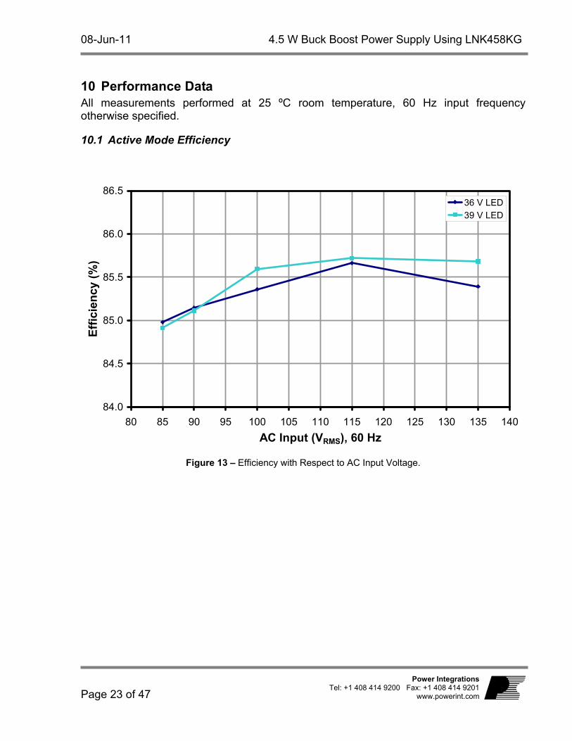
10 Performance Data All measurements performed at 25 ºC room temperature, 60 Hz input frequency otherwise specified.
10.1 Active Mode Efficiency
84.0
84.5
85.0
85.5
86.0
86.5
80 85 90 95 100 105 110 115 120 125 130 135 140
AC Input (VRMS), 60 Hz
Eff
icie
ncy
(%
)
36 V LED39 V LED
Figure 13 – Efficiency with Respect to AC Input Voltage.

RDR-271 4.5 W Buck Boost Power Supply Using LNK458KG 08-Jun-11
Page 24 of 47
Power Integrations, Inc. Tel: +1 408 414 9200 Fax: +1 408 414 9201 www.powerint.com
10.2 Line Regulation
-8
-6
-4
-2
0
2
4
6
8
VAC Input
Reg
ula
tio
n B
and
(%
)
85 - 135 VAC47 - 63 Hz
85 - 135 VAC50 Hz
115 VAC60 Hz
Figure 14 – Line Regulation, Room Temperature.
08-Jun-11 4.5 W Buck Boost Power Supply Using LNK458KG
Page 25 of 47
Power Integrations Tel: +1 408 414 9200 Fax: +1 408 414 9201
www.powerint.com
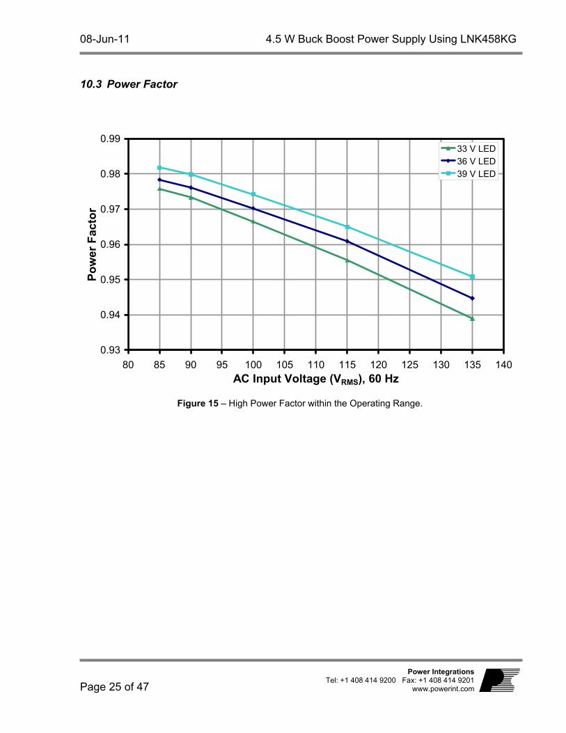
10.3 Power Factor
0.93
0.94
0.95
0.96
0.97
0.98
0.99
80 85 90 95 100 105 110 115 120 125 130 135 140AC Input Voltage (VRMS), 60 Hz
Po
wer
Fac
tor
33 V LED
36 V LED39 V LED
Figure 15 – High Power Factor within the Operating Range.
RDR-271 4.5 W Buck Boost Power Supply Using LNK458KG 08-Jun-11
Page 26 of 47
Power Integrations, Inc. Tel: +1 408 414 9200 Fax: +1 408 414 9201 www.powerint.com
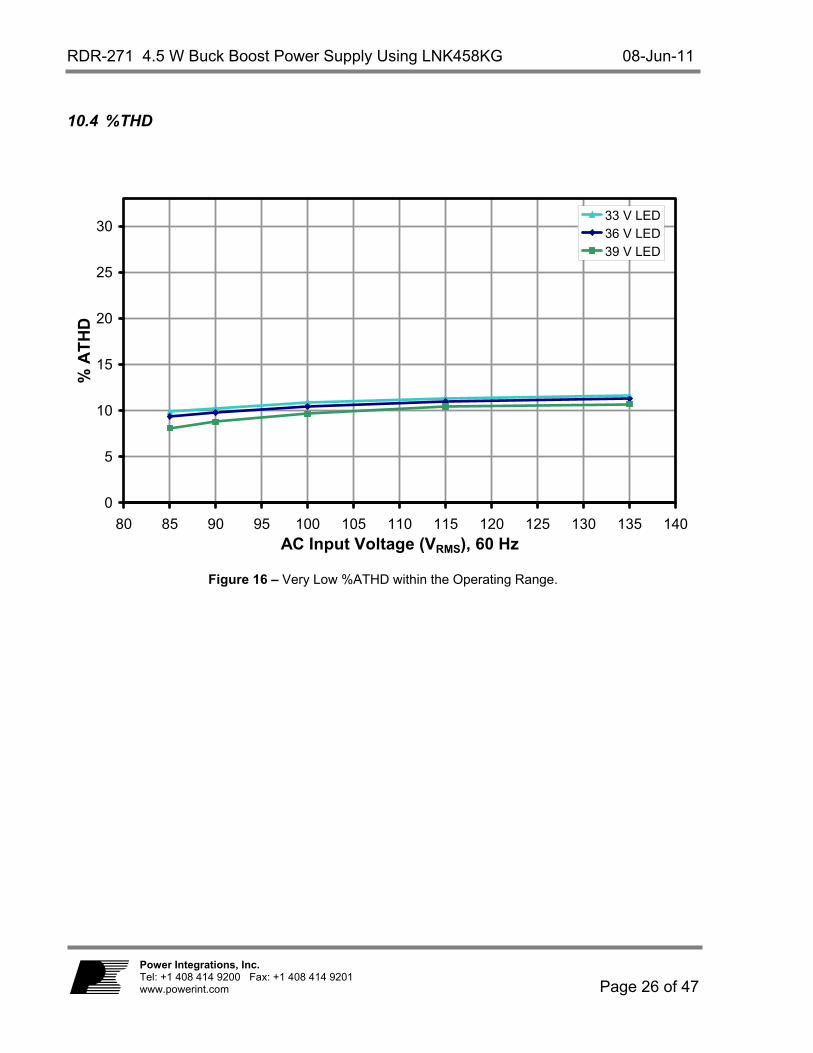
10.4 %THD
0
5
10
15
20
25
30
80 85 90 95 100 105 110 115 120 125 130 135 140AC Input Voltage (VRMS), 60 Hz
% A
TH
D
33 V LED36 V LED39 V LED
Figure 16 – Very Low %ATHD within the Operating Range.
08-Jun-11 4.5 W Buck Boost Power Supply Using LNK458KG
Page 27 of 47
Power Integrations Tel: +1 408 414 9200 Fax: +1 408 414 9201
www.powerint.com
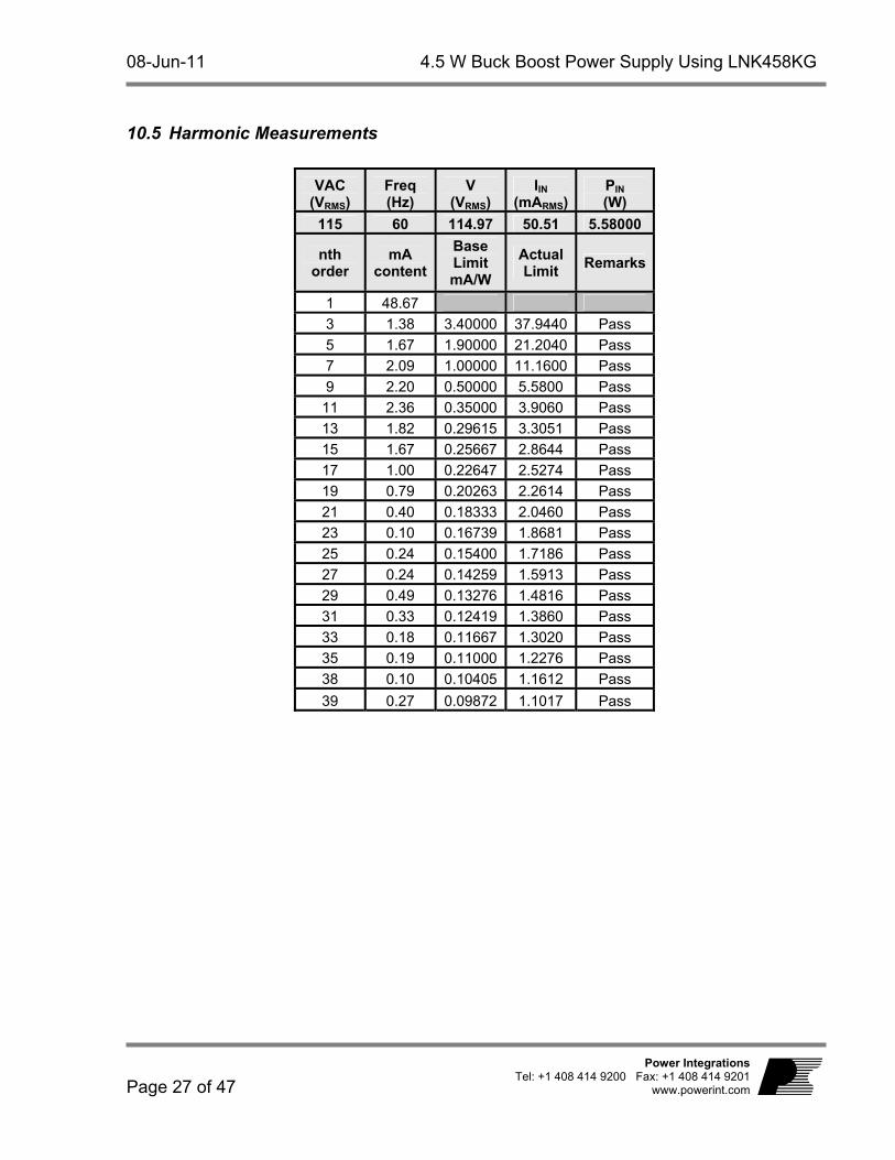
10.5 Harmonic Measurements
VAC (VRMS)
Freq (Hz)
V (VRMS)
IIN (mARMS)
PIN (W)
115 60 114.97 50.51 5.58000
nth order
mA content
Base Limit mA/W
ActualLimit
Remarks
1 48.67
3 1.38 3.40000 37.9440 Pass
5 1.67 1.90000 21.2040 Pass
7 2.09 1.00000 11.1600 Pass
9 2.20 0.50000 5.5800 Pass
11 2.36 0.35000 3.9060 Pass
13 1.82 0.29615 3.3051 Pass
15 1.67 0.25667 2.8644 Pass
17 1.00 0.22647 2.5274 Pass
19 0.79 0.20263 2.2614 Pass
21 0.40 0.18333 2.0460 Pass
23 0.10 0.16739 1.8681 Pass
25 0.24 0.15400 1.7186 Pass
27 0.24 0.14259 1.5913 Pass
29 0.49 0.13276 1.4816 Pass
31 0.33 0.12419 1.3860 Pass
33 0.18 0.11667 1.3020 Pass
35 0.19 0.11000 1.2276 Pass
38 0.10 0.10405 1.1612 Pass
39 0.27 0.09872 1.1017 Pass

RDR-271 4.5 W Buck Boost Power Supply Using LNK458KG 08-Jun-11
Page 28 of 47
Power Integrations, Inc. Tel: +1 408 414 9200 Fax: +1 408 414 9201 www.powerint.com
0
5
10
15
20
25
30
35
40
3 5 7 9 11 13 15 17 19 21 23 25 27 29 31 33 35 37 39Harmonic Order
Har
mo
nic
Co
nte
nt
LimitsMeasured
Figure 17 – Meets EN61000-3-2 Harmonics Contents Standards for <25 W Rating.
08-Jun-11 4.5 W Buck Boost Power Supply Using LNK458KG
Page 29 of 47
Power Integrations Tel: +1 408 414 9200 Fax: +1 408 414 9201
www.powerint.com
11 Thermal Performance
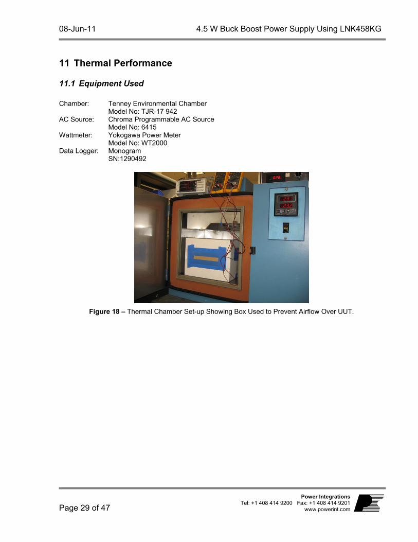
11.1 Equipment Used Chamber: Tenney Environmental Chamber Model No: TJR-17 942 AC Source: Chroma Programmable AC Source Model No: 6415 Wattmeter: Yokogawa Power Meter Model No: WT2000 Data Logger: Monogram SN:1290492
Figure 18 – Thermal Chamber Set-up Showing Box Used to Prevent Airflow Over UUT.

RDR-271 4.5 W Buck Boost Power Supply Using LNK458KG 08-Jun-11
Page 30 of 47
Power Integrations, Inc. Tel: +1 408 414 9200 Fax: +1 408 414 9201 www.powerint.com
11.2 Thermal Results Load: 36 V / 130 mA LED load. Ambient of 90 °C simulates operation inside sealed LED replacement enclosure.
Normal Operation Device Temperature (ºC)Component 85 V/50 Hz 100 V/50Hz 115V/60Hz
Normal OTP Normal OTP Normal OTP Box Internal Ambient (ºC) 90 106 90 113 90 113
Bridge (BR1) 108 120 103 125 102 125 Blocking Diode (D1) 113 125 107 130 106 129
LNK458KG (U1) 120 134 112 134 111 134 Inductor Core (L3) 116 126 108 130 105 130 Output Diode (D2) 126 138 110 132 109 132
Table 1 – Thermal Data if U1 Exposed Pad is Soldered.
Normal Operation Device Temperature (ºC)
Component 85 V/50 Hz 100 V/50Hz 115V/60Hz Normal OTP Normal OTP Normal OTP
Box Internal Ambient (ºC) 90 104 90 107 90 107 Bridge (BR1) 108 118 104 120 104 120
Blocking Diode (D1) 112 124 109 126 110 126 LNK458KG (U1) 125 133 117 135 118 135
Inductor Core (L3) 115 124 108 126 110 126 Output Diode (D2) 122 127 112 129 113 129
Table 2 – Thermal Data if U1 Exposed Pad is Unsoldered.

08-Jun-11 4.5 W Buck Boost Power Supply Using LNK458KG
Page 31 of 47
Power Integrations Tel: +1 408 414 9200 Fax: +1 408 414 9201
www.powerint.com
12 Thermal Scans The scan is conducted at ambient temperature of 25 ºC, 85 VAC / 47 Hz input and 35 V LED string load.
Figure 19 – U1 Case Temperature. Figure 20 – D2 Case Temperature.
Figure 21 – L3 Temperature. Figure 22 – BR1 Case Temperature.

RDR-271 4.5 W Buck Boost Power Supply Using LNK458KG 08-Jun-11
Page 32 of 47
Power Integrations, Inc. Tel: +1 408 414 9200 Fax: +1 408 414 9201 www.powerint.com
13 Waveforms
13.1 Drain Voltage and Current, Normal Operation
Figure 23 – 85 VAC / 47 Hz, 35 V LED String. Ch1: VDRAIN, 50 V / div. Ch2: VSOURCE, 50 V / div. Ch4: IDRAIN, 0.5 A / div. F1: VD-S, 100 V / div., 2 s / div.
Figure 24 – 85 VAC / 47 Hz, 35 V LED String. Ch1: VDRAIN, 100 V / div. Ch2: VSOURCE, 100 V / div. Ch4: IDRAIN, 0.5 A / div. F1: VD-S, 100 V / div., 2 ms / div.
Figure 25 – 100 VAC / 50 Hz, 35 V LED String. Ch1: VDRAIN, 50 V / div. Ch2: VSOURCE, 50 V / div. Ch4: IDRAIN, 0.5 A / div. F1: VD-S, 100 V / div., 2 s / div.
Figure 26 – 115 VAC / 60 Hz, 35 V LED String. Ch1: VDRAIN, 50 V / div. Ch2: VSOURCE, 50 V / div. Ch4: IDRAIN, 0.5 A / div. F1: VD-S, 100 V / div., 2 s / div.
08-Jun-11 4.5 W Buck Boost Power Supply Using LNK458KG
Page 33 of 47
Power Integrations Tel: +1 408 414 9200 Fax: +1 408 414 9201
www.powerint.com
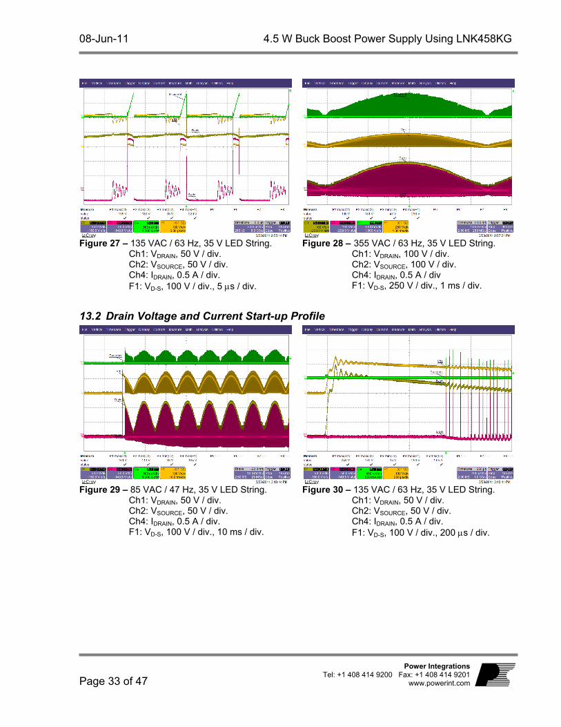
Figure 27 – 135 VAC / 63 Hz, 35 V LED String. Ch1: VDRAIN, 50 V / div. Ch2: VSOURCE, 50 V / div. Ch4: IDRAIN, 0.5 A / div. F1: VD-S, 100 V / div., 5 s / div.
Figure 28 – 355 VAC / 63 Hz, 35 V LED String. Ch1: VDRAIN, 100 V / div. Ch2: VSOURCE, 100 V / div. Ch4: IDRAIN, 0.5 A / div F1: VD-S, 250 V / div., 1 ms / div.
13.2 Drain Voltage and Current Start-up Profile
Figure 29 – 85 VAC / 47 Hz, 35 V LED String. Ch1: VDRAIN, 50 V / div. Ch2: VSOURCE, 50 V / div. Ch4: IDRAIN, 0.5 A / div. F1: VD-S, 100 V / div., 10 ms / div.
Figure 30 – 135 VAC / 63 Hz, 35 V LED String. Ch1: VDRAIN, 50 V / div. Ch2: VSOURCE, 50 V / div. Ch4: IDRAIN, 0.5 A / div. F1: VD-S, 100 V / div., 200 s / div.
RDR-271 4.5 W Buck Boost Power Supply Using LNK458KG 08-Jun-11
Page 34 of 47
Power Integrations, Inc. Tel: +1 408 414 9200 Fax: +1 408 414 9201 www.powerint.com
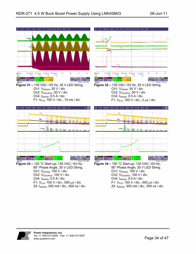
Figure 31 – 135 VAC / 63 Hz, 35 V LED String. Ch1: VDRAIN, 50 V / div. Ch2: VSOURCE, 50 V / div. Ch4: IDRAIN, 0.5 A / div. F1: VD-S, 100 V / div., 10 ms / div.
Figure 32 – 135 VAC / 63 Hz, 35 V LED String. Ch1: VDRAIN, 50 V / div. Ch2: VSOURCE, 50 V / div. Ch4: IDRAIN, 0.5 A / div. F1: VD-S, 100 V / div., 2 s / div.
Figure 33 – 125 °C Start-up; 135 VAC / 63 Hz; 85° Phase Angle, 35 V LED String. Ch1: VDRAIN, 100 V / div. Ch2: VSOURCE, 100 V / div. Ch4: IDRAIN, 0.5 A / div. F1: VD-S, 100 V / div., 500 s / div. Z4: IDRAIN, 305 mA / div.; 500 ns / div.
Figure 34 – 150 °C Start-up; 135 VAC / 63 Hz; 85° Phase Angle, 35 V LED String. Ch1: VDRAIN, 100 V / div. Ch2: VSOURCE, 100 V / div. Ch4: IDRAIN, 0.5 A / div. F1: VD-S, 100 V / div., 500 s / div. Z4: IDRAIN, 305 mA / div.; 500 ns / div.

08-Jun-11 4.5 W Buck Boost Power Supply Using LNK458KG
Page 35 of 47
Power Integrations Tel: +1 408 414 9200 Fax: +1 408 414 9201
www.powerint.com
13.3 Output Voltage Start-up Profile
Figure 35 – 85 VAC / 47 Hz, 35 V LED String. Ch1: VIN, 50 V / div. Ch2: VOUT, 10 V / div. Ch3: IIN, 50 mA / div. Ch4: IOUT, 50 mA / div., 50 ms / div.
Figure 36 – 135 VAC / 63 Hz, 35 V LED String. Ch1: VIN, 50 V / div. Ch2: VOUT, 10 V / div. Ch3: IIN, 50 m A / div. Ch4: IOUT, 50 mA / div., 50 ms / div.
RDR-271 4.5 W Buck Boost Power Supply Using LNK458KG 08-Jun-11
Page 36 of 47
Power Integrations, Inc. Tel: +1 408 414 9200 Fax: +1 408 414 9201 www.powerint.com
13.4 Drain Voltage and Current Start-up Short Profile
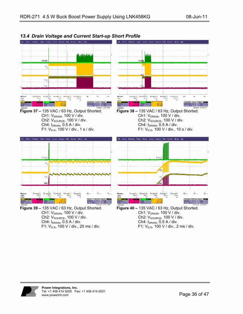
Figure 37 – 135 VAC / 63 Hz, Output Shorted. Ch1: VDRAIN, 100 V / div. Ch2: VSOURCE, 100 V / div. Ch4: IDRAIN, 0.5 A / div. F1: VD-S, 100 V / div., 1 s / div.
Figure 38 – 135 VAC / 63 Hz, Output Shorted. Ch1: VDRAIN, 100 V / div. Ch2: VSOURCE, 100 V / div. Ch4: IDRAIN, 0.5 A / div. F1: VD-S, 100 V / div., 10 s / div.
Figure 39 – 135 VAC / 63 Hz, Output Shorted. Ch1: VDRAIN, 100 V / div. Ch2: VSOURCE, 100 V / div. Ch4: IDRAIN, 0.5 A / div. F1: VD-S, 100 V / div., 20 ms / div.
Figure 40 – 135 VAC / 63 Hz, Output Shorted. Ch1: VDRAIN, 100 V / div. Ch2: VSOURCE, 100 V / div. Ch4: IDRAIN, 0.5 A / div. F1: VD-S, 100 V / div., 2 ms / div.
08-Jun-11 4.5 W Buck Boost Power Supply Using LNK458KG
Page 37 of 47
Power Integrations Tel: +1 408 414 9200 Fax: +1 408 414 9201
www.powerint.com
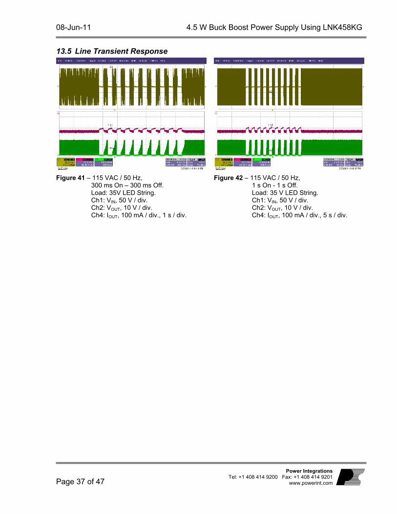
13.5 Line Transient Response
Figure 41 – 115 VAC / 50 Hz, 300 ms On – 300 ms Off. Load: 35V LED String. Ch1: VIN, 50 V / div. Ch2: VOUT, 10 V / div. Ch4: IOUT, 100 mA / div., 1 s / div.
Figure 42 – 115 VAC / 50 Hz, 1 s On - 1 s Off. Load: 35 V LED String. Ch1: VIN, 50 V / div. Ch2: VOUT, 10 V / div. Ch4: IOUT, 100 mA / div., 5 s / div.
RDR-271 4.5 W Buck Boost Power Supply Using LNK458KG 08-Jun-11
Page 38 of 47
Power Integrations, Inc. Tel: +1 408 414 9200 Fax: +1 408 414 9201 www.powerint.com
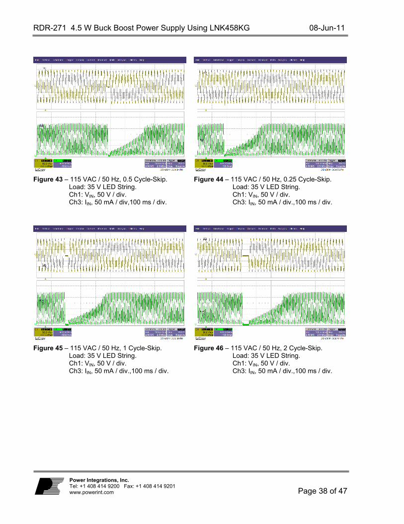
Figure 43 – 115 VAC / 50 Hz, 0.5 Cycle-Skip. Load: 35 V LED String. Ch1: VIN, 50 V / div. Ch3: IIN, 50 mA / div,100 ms / div.
Figure 44 – 115 VAC / 50 Hz, 0.25 Cycle-Skip. Load: 35 V LED String. Ch1: VIN, 50 V / div. Ch3: IIN, 50 mA / div.,100 ms / div.
Figure 45 – 115 VAC / 50 Hz, 1 Cycle-Skip. Load: 35 V LED String. Ch1: VIN, 50 V / div. Ch3: IIN, 50 mA / div.,100 ms / div.
Figure 46 – 115 VAC / 50 Hz, 2 Cycle-Skip. Load: 35 V LED String. Ch1: VIN, 50 V / div. Ch3: IIN, 50 mA / div.,100 ms / div.
08-Jun-11 4.5 W Buck Boost Power Supply Using LNK458KG
Page 39 of 47
Power Integrations Tel: +1 408 414 9200 Fax: +1 408 414 9201
www.powerint.com
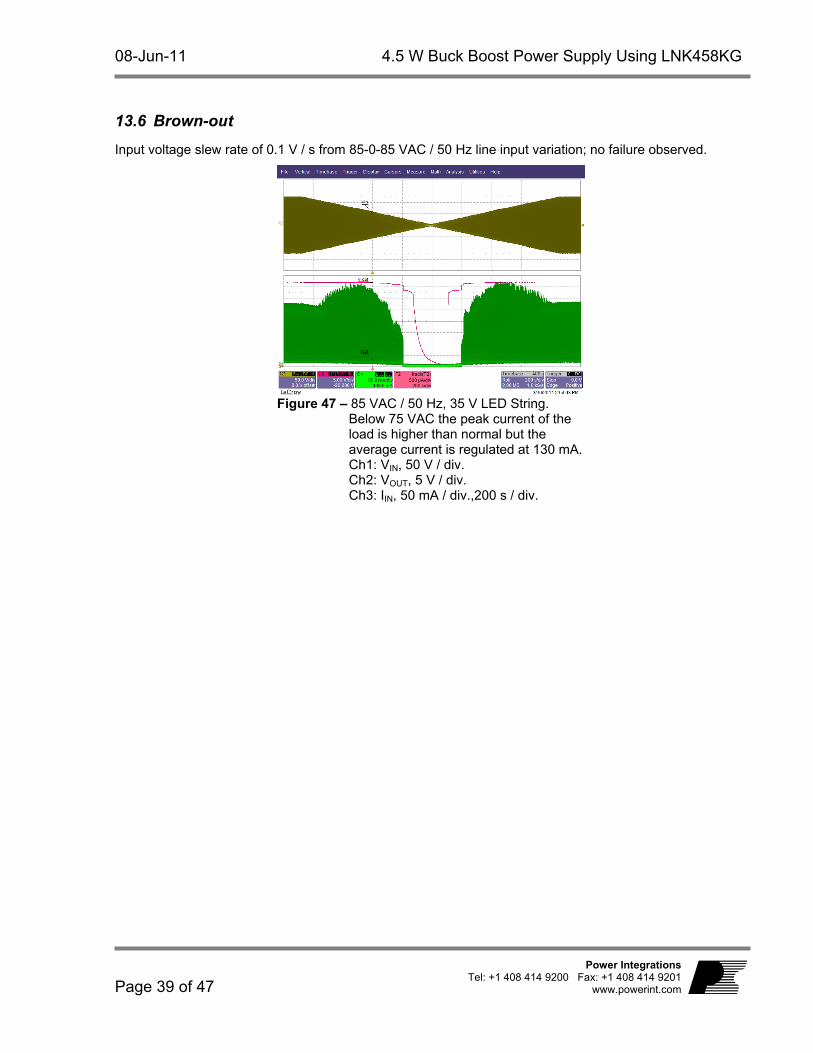
13.6 Brown-out
Input voltage slew rate of 0.1 V / s from 85-0-85 VAC / 50 Hz line input variation; no failure observed.
Figure 47 – 85 VAC / 50 Hz, 35 V LED String.
Below 75 VAC the peak current of the load is higher than normal but the average current is regulated at 130 mA. Ch1: VIN, 50 V / div. Ch2: VOUT, 5 V / div. Ch3: IIN, 50 mA / div.,200 s / div.
RDR-271 4.5 W Buck Boost Power Supply Using LNK458KG 08-Jun-11
Page 40 of 47
Power Integrations, Inc. Tel: +1 408 414 9200 Fax: +1 408 414 9201 www.powerint.com
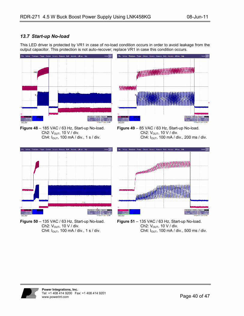
13.7 Start-up No-load
This LED driver is protected by VR1 in case of no-load condition occurs in order to avoid leakage from the output capacitor. This protection is not auto-recover; replace VR1 in case this condition occurs.
Figure 48 – 185 VAC / 63 Hz, Start-up No-load. Ch2: VOUT, 10 V / div. Ch4: IOUT, 100 mA / div., 1 s / div.
Figure 49 – 85 VAC / 63 Hz, Start-up No-load. Ch2: VOUT, 10 V / div. Ch4: IOUT, 100 mA / div., 200 ms / div.
Figure 50 – 135 VAC / 63 Hz, Start-up No-load. Ch2: VOUT, 10 V / div. Ch4: IOUT, 100 mA / div., 1 s / div.
Figure 51 – 135 VAC / 63 Hz, Start-up No-load. Ch2: VOUT, 10 V / div. Ch4: IOUT, 100 mA / div., 500 ms / div.

08-Jun-11 4.5 W Buck Boost Power Supply Using LNK458KG
Page 41 of 47
Power Integrations Tel: +1 408 414 9200 Fax: +1 408 414 9201
www.powerint.com
13.8 Line Surge Waveform
Figure 52 – 115 VAC / 60 Hz, 500 V Differential Surge. Ch1: VIN, 200 V / div. Ch2: VDRAIN, 10 V / div. Ch3: VSOURCE, 10 V / div. F1: VDS, 500 V / div., 50 s / div.
Figure 53 – 115 VAC / 60 Hz, 1 kV Differential Surge; VR2 Installed. Ch1: VIN, 200 V / div. Ch2: VDRAIN, 10 V / div. Ch3: VSOURCE, 10 V / div. F1: VDS, 500V / div., 50 s / div.

RDR-271 4.5 W Buck Boost Power Supply Using LNK458KG 08-Jun-11
Page 42 of 47
Power Integrations, Inc. Tel: +1 408 414 9200 Fax: +1 408 414 9201 www.powerint.com
14 Line Surge Input voltage was set at 115 VAC / 60 Hz. Output was loaded with 35 V LED string and operation was verified following each surge event. Differential input line 1.2 / 50 s surge testing was completed on two test unit to IEC61000-4-5.
Surge Level (V)
Input Voltage (VAC)
Injection Location
Injection Phase
(°)
Test Result (Pass/Fail)
Option 1: VR2 not installed +500 115 L to N 0 Pass -500 115 L to N 0 Pass +500 115 L to N 90 Pass -500 115 L to N 90 Pass
Option 2: VR2 installed +1200 115 L to N 0 Pass -1200 115 L to N 0 Pass +1200 115 L to N 90 Pass -1200 115 L to N 90 Pass
Differential input line ring surge testing was completed on two test unit to IEC61000-4-5.
Surge Level (V)
Input Voltage (VAC)
Injection Location
Injection Phase
(°)
Test Result (Pass/Fail)
Option 1: VR2 not installed +2500 115 L to N 0 Pass -2500 115 L to N 0 Pass +2500 115 L to N 90 Pass -2500 115 L to N 90 Pass +3000 115 L to N 0 Pass -3000 115 L to N 0 Pass +3000 115 L to N 90 Pass -3000 115 L to N 90 Pass
Unit passes under all test conditions.
08-Jun-11 4.5 W Buck Boost Power Supply Using LNK458KG
Page 43 of 47
Power Integrations Tel: +1 408 414 9200 Fax: +1 408 414 9201
www.powerint.com
15 Conducted EMI
15.1 Equipment: Receiver:
Rohde & Schwartz ESPI - Test Receiver (9 kHz – 3 GHz) Model No: ESPI3
LISN: Rohde & Schwartz Two-Line-V-Network Model No: ENV216
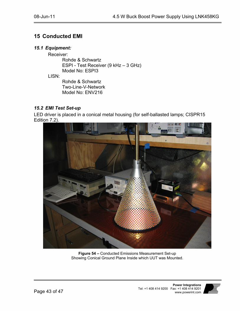
15.2 EMI Test Set-up LED driver is placed in a conical metal housing (for self-ballasted lamps; CISPR15 Edition 7.2).
Figure 54 – Conducted Emissions Measurement Set-up
Showing Conical Ground Plane Inside which UUT was Mounted.

RDR-271 4.5 W Buck Boost Power Supply Using LNK458KG 08-Jun-11
Page 44 of 47
Power Integrations, Inc. Tel: +1 408 414 9200 Fax: +1 408 414 9201 www.powerint.com
Power Integrations
SGL
TDF
6DB
9 kHz 30 MHz
dBµV dBµV
2 AVCLRWR
1 QPCLRWR
24.Mar 11 13:18
RBW 9 kHz
MT 500 ms
Att 10 dB AUTO
100 kHz 1 MHz 10 MHz
-20
-10
0
10
20
30
40
50
60
70
80
90
100
110
120
LIMIT CHECK PASS
EN55015A
EN55015Q
Figure 55 – Conducted EMI, Maximum Steady-State Load, 115 VAC, 60 Hz, and EN55015 Limits.
08-Jun-11 4.5 W Buck Boost Power Supply Using LNK458KG
Page 45 of 47
Power Integrations Tel: +1 408 414 9200 Fax: +1 408 414 9201
www.powerint.com
EDIT PEAK LIST (Final Measurement Results)
Trace1: EN55015Q
Trace2: EN55015A
Trace3: ---
TRACE FREQUENCY LEVEL dBµV DELTA LIMIT dB
2 Average 95.14984736 kHz 14.69 L1 gnd
2 Average 99.0133127137 kHz 8.86 N gnd
1 Quasi Peak 190.46019728 kHz 45.86 N gnd -18.15
2 Average 192.364799253 kHz 37.68 N gnd -16.25
1 Quasi Peak 283.569280422 kHz 42.86 N gnd -17.84
2 Average 289.269022958 kHz 36.17 N gnd -14.36
1 Quasi Peak 378.424303998 kHz 43.21 N gnd -15.09
2 Average 389.890938834 kHz 33.37 N gnd -14.69
1 Quasi Peak 881.64914842 kHz 42.69 N gnd -13.30
2 Average 881.64914842 kHz 30.42 N gnd -15.57
1 Quasi Peak 983.628047757 kHz 36.36 N gnd -19.63
1 Quasi Peak 1.17656420634 MHz 42.34 N gnd -13.65
2 Average 1.17656420634 MHz 31.30 N gnd -14.69
2 Average 1.23658080545 MHz 31.28 N gnd -14.71
1 Quasi Peak 1.27405044044 MHz 41.86 N gnd -14.13
2 Average 1.33903981723 MHz 31.57 N gnd -14.42
1 Quasi Peak 1.37961406273 MHz 36.63 N gnd -19.36
1 Quasi Peak 1.43563192593 MHz 44.42 N gnd -11.57
2 Average 1.43563192593 MHz 31.34 N gnd -14.65
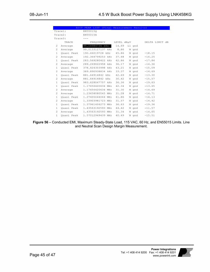
1 Quasi Peak 1.57012949439 MHz 40.49 N gnd -15.51 Figure 56 – Conducted EMI, Maximum Steady-State Load, 115 VAC, 60 Hz, and EN55015 Limits. Line
and Neutral Scan Design Margin Measurement.

RDR-271 4.5 W Buck Boost Power Supply Using LNK458KG 08-Jun-11
Page 46 of 47
Power Integrations, Inc. Tel: +1 408 414 9200 Fax: +1 408 414 9201 www.powerint.com
16 Revision History Date Author Revision Description & changes Reviewed 08-Jun-11 JDC 1.0 Initial Release Apps & Mktg

08-Jun-11 4.5 W Buck Boost Power Supply Using LNK458KG
Page 47 of 47
Power Integrations Tel: +1 408 414 9200 Fax: +1 408 414 9201
www.powerint.com
For the latest updates, visit our website: www.powerint.com Power Integrations reserves the right to make changes to its products at any time to improve reliability or manufacturability. Power Integrations does not assume any liability arising from the use of any device or circuit described herein. POWER INTEGRATIONS MAKES NO WARRANTY HEREIN AND SPECIFICALLY DISCLAIMS ALL WARRANTIES INCLUDING, WITHOUT LIMITATION, THE IMPLIED WARRANTIES OF MERCHANTABILITY, FITNESS FOR A PARTICULAR PURPOSE, AND NON-INFRINGEMENT OF THIRD PARTY RIGHTS.
PATENT INFORMATION The products and applications illustrated herein (including transformer construction and circuits external to the products) may be covered by one or more U.S. and foreign patents, or potentially by pending U.S. and foreign patent applications assigned to Power Integrations. A complete list of Power Integrations’ patents may be found at www.powerint.com. Power Integrations grants its customers a license under certain patent rights as set forth at http://www.powerint.com/ip.htm. The PI Logo, TOPSwitch, TinySwitch, LinkSwitch, DPA-Switch, PeakSwitch, CAPZero, SENZero, LinkZero, HiperPFS, HiperTFS, Qspeed, EcoSmart, Clampless, E-Shield, Filterfuse, StackFET, PI Expert and PI FACTS are trademarks of Power Integrations, Inc. Other trademarks are property of their respective companies. ©Copyright 2011 Power Integrations, Inc.
Power Integrations Worldwide Sales Support Locations
WORLD HEADQUARTERS 5245 Hellyer Avenue San Jose, CA 95138, USA. Main: +1-408-414-9200 Customer Service: Phone: +1-408-414-9665 Fax: +1-408-414-9765 e-mail: [email protected]
GERMANY Rueckertstrasse 3 D-80336, Munich Germany Phone: +49-89-5527-3911 Fax: +49-89-5527-3920 e-mail: [email protected]
JAPAN Kosei Dai-3 Building 2-12-11, Shin-Yokohama, Kohoku-ku, Yokohama-shi, Kanagawa 222-0033 Japan Phone: +81-45-471-1021 Fax: +81-45-471-3717 e-mail: [email protected]
17 TAIWAN 5F, No. 318, Nei Hu Rd., Sec. 1 Nei Hu District Taipei 114, Taiwan R.O.C. Phone: +886-2-2659-4570 Fax: +886-2-2659-4550 e-mail: [email protected]
CHINA (SHANGHAI) Rm 1601/1610, Tower 1 Kerry Everbright City No. 218 Tianmu Road West Shanghai, P.R.C. 200070 Phone: +86-021-6354-6323 Fax: +86-021-6354-6325
e-mail: [email protected]
INDIA #1, 14th Main Road Vasanthanagar Bangalore-560052 India Phone: +91-80-4113-8020 Fax: +91-80-4113-8023 e-mail: [email protected]
KOREA RM 602, 6FL Korea City Air Terminal B/D, 159-6 Samsung-Dong, Kangnam-Gu, Seoul, 135-728 Korea Phone: +82-2-2016-6610 Fax: +82-2-2016-6630 e-mail: [email protected]
EUROPE HQ 1st Floor, St. James’s House East Street, Farnham Surrey GU9 7TJ United Kingdom Phone: +44 (0) 1252-730-141 Fax: +44 (0) 1252-727-689 e-mail: [email protected]
CHINA (SHENZHEN) Rm A, B & C 4th Floor, Block C, Electronics Science and Technology Building 2070 Shennan Zhong Road Shenzhen, Guangdong, P.R.C. 518031 Phone: +86-755-8379-3243 Fax: +86-755-8379-5828 e-mail: [email protected]
ITALY Via De Amicis 2 20091 Bresso MI Italy Phone: +39-028-928-6000 Fax: +39-028-928-6009 e-mail: [email protected]
SINGAPORE 51 Newton Road, #19-01/05 Goldhill Plaza Singapore, 308900 Phone: +65-6358-2160 Fax: +65-6358-2015 e-mail: [email protected]
APPLICATIONS HOTLINE World Wide +1-408-414-9660 APPLICATIONS FAX World Wide +1-408-414-9760