book of abstracts 262 ptb seminar euv metrology · 2011-10-19 · 262nd ptb seminar euv metrology...
TRANSCRIPT

Physikalisch-Technische BundesanstaltInstitut Berlin
Book of Abstracts
262nd PTB SeminarEUV MetrologyOctober 27th - 28th, 2011Berlin
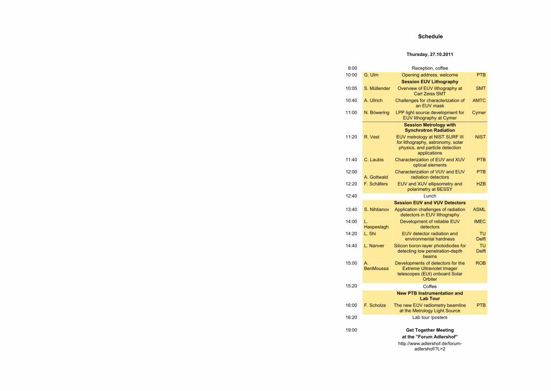
Schedule
Thursday, 27.10.2011
9:00 Reception, coffee 10:00 G. Ulm Opening address, welcome PTB
Session EUV Lithography 10:05 S. Müllender Overview of EUV lithography at
Carl Zeiss SMT SMT
10:40 A. Ullrich Challenges for characterization of an EUV mask
AMTC
11:00 N. Böwering LPP light source development for EUV lithography at Cymer
Cymer
Session Metrology with Synchrotron Radiation
11:20 R. Vest EUV metrology at NIST SURF III for lithography, astronomy, solar physics, and particle detection
applications
NIST
11:40 C. Laubis Characterization of EUV and XUV optical elements
PTB
12:00A. Gottwald
Characterization of VUV and EUV radiation detectors
PTB
12:20 F. Schäfers EUV and XUV ellipsometry and polarimetry at BESSY
HZB
12:40 Lunch Session EUV and VUV Detectors
13:40 S. Nihtianov Application challenges of radiation detectors in EUV lithography
ASML
14:00 L. Haspeslagh
Development of reliable EUV detectors
IMEC
14:20 L. Shi EUV detector radiation and environmental hardness
TU Delft
14:40 L. Nanver Silicon boron-layer photodiodes for detecting low penetration-depth
beams
TU Delft
15:00 A. BenMoussa
Developments of detectors for the Extreme Ultraviolet Imager
telescopes (EUI) onboard Solar Orbiter
ROB
15:20 Coffee New PTB Instrumentation and
Lab Tour
16:00 F. Scholze The new EUV radiometry beamline at the Metrology Light Source
PTB
16:20 Lab tour /posters
19:00 Get Together Meeting at the ”Forum Adlershof”
http://www.adlershof.de/forum-adlershof/?L=2
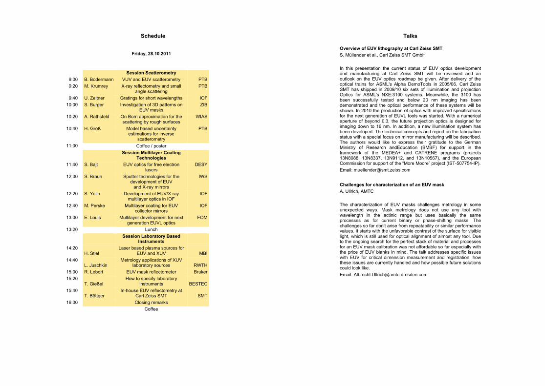
Schedule
Friday, 28.10.2011
Session Scatterometry
9:00 B. Bodermann VUV and EUV scatterometry PTB 9:20 M. Krumrey X-ray reflectometry and small
angle scattering PTB
9:40 U. Zeitner Gratings for short wavelengths IOF 10:00 S. Burger Investigation of 3D patterns on
EUV masks ZIB
10:20 A. Rathsfeld On Born approximation for the scattering by rough surfaces
WIAS
10:40 H. Groß Model based uncertainty estimations for inverse
scatterometry
PTB
11:00 Coffee / poster Session Multilayer Coating
Technologies 11:40 S. Bajt EUV optics for free electron
lasers DESY
12:00 S. Braun Sputter technologies for the development of EUV
and X-ray mirrors
IWS
12:20 S. Yulin Development of EUV/X-ray multilayer optics in IOF
IOF
12:40 M. Perske Multilayer coating for EUV collector mirrors
IOF
13:00 E. Louis Multilayer development for next generation EUVL optics
FOM
13:20 Lunch Session Laboratory Based
Instruments
14:20 H. Stiel
Laser based plasma sources for EUV and XUV MBI
14:40 L. Juschkin
Metrology applications of XUV laboratory sources RWTH
15:00 R. Lebert EUV mask reflectometer Bruker 15:20
T. Gießel How to specify laboratory
instruments BESTEC 15:40
T. Böttger In-house EUV reflectometry at
Carl Zeiss SMT SMT 16:00 Closing remarks
Coffee
Talks Overview of EUV lithography at Carl Zeiss SMTS. Müllender et al., Carl Zeiss SMT GmbH In this presentation the current status of EUV optics development and manufacturing at Carl Zeiss SMT will be reviewed and an outlook on the EUV optics roadmap be given. After delivery of the optical trains for ASML's Alpha DemoTools in 2005/06, Carl Zeiss SMT has shipped in 2009/10 six sets of illumination and projection Optics for ASML's NXE:3100 systems. Meanwhile, the 3100 has been successfully tested and below 20 nm imaging has been demonstrated and the optical performance of these systems will be shown. In 2010 the production of optics with improved specifications for the next generation of EUVL tools was started. With a numerical aperture of beyond 0.3, the future projection optics is designed for imaging down to 16 nm. In addition, a new illumination system has been developed. The technical concepts and report on the fabrication status with a special focus on mirror manufacturing will be described. The authors would like to express their gratitude to the German Ministry of Research andEducation (BMBF) for support in the framework of the MEDEA+ and CATRENE programs (projects 13N8088, 13N8337, 13N9112, and 13N10567), and the European Commission for support of the “More Moore” project (IST-507754-IP). Email: [email protected]
Challenges for characterization of an EUV mask A. Ullrich, AMTC The characterization of EUV masks challenges metrology in some unexpected ways. Mask metrology does not use any tool with wavelength in the actinic range but uses basically the same processes as for current binary or phase-shifting masks. The challenges so far don't arise from repeatability or similar performance values. It starts with the unfavorable contrast of the surface for visible light, which is still used for optical alignment of almost any tool. Due to the ongoing search for the perfect stack of material and processes for an EUV mask calibration was not affordable so far especially with the price of EUV blanks in mind. The talk addresses specific issues with EUV for critical dimension measurement and registration, how these issues are currently handled and how possible future solutions could look like. Email: [email protected]
LPP light source development for EUV lithography at Cymer N. Böwering, EUV Technology Cymer Europe Laser produced plasma (LPP) light source systems have been developed as the primary approach for EUV scanner optical imaging of circuit features of sub-22 nm critical layer patterning in support of high-throughput semiconductor lithography. The components and the development of CO2-laser based light source architecture for advanced lithography applications are described. A review is provided of development progress and productization, as well as of installation and operational status for high-volume manufacturing LPP EUV light sources at Cymer. Measurements are presented for a production system with stable tin droplet generation, efficient gas-based debris mitigation system and large 5 sr normal-incidence light collector optics. Latest results are reported on high average power testing, stable light collection, and clean transmission through intermediate focus for pilot sources, including data on dose stability and out-of band radiation at high EUV average power levels. Power scaling was demonstrated on a separate test configuration using a laser pre-pulse to optimize the plasma conditions reaching burst power levels of 160 W. The lifetime of the collector is a critical parameter for such sources. It was shown to be significantly enhanced, supporting uninterrupted operation for several weeks, by use of protective cap layers on the multilayer coating. Email: [email protected]
EUV metrology at NIST SURF III for lithography, astronomy, solar physics, and particle detection applications R. E. Vest, NIST, Gaithersburg, Maryland The National Institute of Standards and Technology (NIST) operates the Synchrotron Ultraviolet Radiation Facility (SURF III) to support a number of applications of extreme ultraviolet radiation. SURF III is a 400 MeV electron storage ring that can operate in a number of special modes optimized for radiometry and metrology. In this talk, I will describe the synchrotron radiation facility and some of the recent applications, including photoresist contamination characterization, absorption spectroscopy of BF3 for neutron detection, low-flux calibration of photomultiplier tubes, calibration of space-based instrumentation, and our transfer standard photodiode program for dissemination of the U.S. national scale of detector responsivity in the EUV. Email: [email protected]
Characterization of EUV and XUV optical elements C. Laubis, Physikalisch-Technische Bundesanstalt PTB provides measurements services using synchrotron radiation at the storage rings BESSY I and BESSY II for the characterization of multilayer mirrors and other optical elements in the EUV and soft X-ray spectral ranges for more than 25 years. The measurement capabilities evolved in parallel with the measurement challenges from industry and science. We are now able to provide polarization resolved measurements, mappings on curved mirror surfaces as well as the standard wavelength- or angle-of-incidence-scans for specimen up to 670 mm in diameter and 50 kg in weight. Apart from basic specular reflectometry we also use scatterometry to gain information on surface roughness or structures. And last not least, we regularly characterize detectors and gratings or even complete space instruments as well as for the characterization of pulsed plasma EUV sources. An overview of all these activities is given. Email: [email protected]
Characterization of VUV and EUV radiation detectors A. Gottwald, Physikalisch-Technische Bundesanstalt The characterization of radiation detectors at PTB is based on the capability to measure the detector’s spectral responsivity in absolute units. This is done by calibrations traceable to cryogenic radiometers as primary detector standards. By the use of monochromatized synchrotron radiation, PTB offers a scale of spectral responsivity between 0.1 nm to 400 nm which is realized using different types of semiconductor photodiodes. Although the uncertainties in calibration are typically well below 1 %, in particular the VUV spectral range shows larger uncertainties, mainly due to the critical performance of available standard detectors. Besides absolute calibrations, it is therefore needed that radiation detectors are characterized regarding e.g. their area uniformity, linearity, and degradation under irradiation. This is not only done for single photodetectors, but also for imaging devices like CCDs. For high-sensitive, photon-counting devices the large dynamic range of the synchrotron radiation is used, which allow the intensity to be changed by up to 11 orders of magnitude without changing the spectral distribution of the radiation. Email: [email protected]
EUV and XUV ellipsometry and polarimetry at BESSY F. Schäfers, Helmholtz-Zentrum Berlin, Institute for Nanometre Optics and Technology
Soft x-ray synchrotron radiation with variable polarisation is a sophisticated probe of the physical properties of matter. Many of the most advanced experiments take advantage of the inherently high degree of linear and/or circular polarisation of such a source which is in general an elliptical undulator. Polarimeters designed to deliver the complete polarisation state, i.e. the four Stokes parameters of a photon beam rely on a phase retarder and analyser in combination [1]. Multilayer phase retarders have been designed to be used near the 2p absorption edges of the constituting materials (Mo/Si, Cr/C, Cr/Sc, Ni/Ti, and Ni/V) [1] because of the resonant enhancement of the multilayer performance there. Thus these optical elements are monoenergetic in the range between 100 eV and 600 eV. At best they can operate at two distinctive energies (e.g. Sc 397 eV and Cr 550 eV) [2]. Newly developed W/B4C phase retarders have a working range from ~600 eV to ~1000 eV, the range of the 2p edges of Fe, Co and Ni, where most of the polarisation-sensitive magneto-optical research is carried out and which was previously not accessible for circular polarisation analysis without further modelling [3]. This self-calibrating polarimetry is in-turn capable of characterising (multilayer) optics with respect to the complex reflection coefficient, i.e. it delivers amplitudes and phase shifts for transmitting and reflecting samples. References [1] F. Schäfers et al., “A soft x-ray polarimeter using multilayer optics: Complete analysis of the polarization state of light”, Applied Optics 38, 4074-4088 (1999) [2] H. Kimura et al., “Transmission type Sc/Cr multilayer as a quarter-wave plate for near 400 eV”, Spectrosc. Relat. Phenom. 144, 1079 (2005) [3] M.A. MacDonald et al., A single W/B4C transmission multilayer for polarization analysis of soft x-rays up to 1 keV, Optics Express Vol. 17, Iss. 25, 23290–23298 (2009) Email: [email protected]
Application challenges of radiation detectors in EUV lithography S. Nihtianov, ASML The main applications of EUV photodetectors in EUV lithographic machines are in metrology modules responsible for the timely delivery of a well-defined EUV amount of energy (doze) to a specific point on the silicon wafer under exposure. These modules are: doze control, alignment and image quality control. The challenges are numerous and have different origin. Some are typical for any industrial application of detectors, others are common for all EUV litho applications, and third are application specific. In the presentation all three groups of challenges will be discussed and specific examples will be given. Most important are the application specific requirements, which in most of the cases prevent using off-the-shelf detectors and pose a broad range of problems already at design and qualification level. Typical requirements are: exotic geometry, integrated different functions on the same die, three-dimensional structures (MOEMS), very-high sensitivity to EUV irradiation, blindness to out-of-spectrum irradiation, very accurate and stable responsivity with time and exposure, extremely uniform responsivity over the active surface of the detector also when there is a multiple-layer filtering- and absorbing-stack on top of the diode surface, short response time, close to zero dark current in life time, work in vacuum and in aggressive environments, machine-lifetime reliability, etc. Although the design and the qualification challenges are not considered application challenges, they are closely related. If the detector performance cannot be guaranteed by design and cannot be measured, then we have performance uncertainty which is an application challenge. This topic will be discussed in the presentation, as well. Email: [email protected]
Development of reliable EUV detectors L. Haspeslagh, IMEC Integrated EUV photodiodes have been developed in collaboration with ASML to serve as alignment and dose sensors for their NXE series EUV scanners. The photodiode is based on the work previously published by DIMES where the shallow p-type top junction is formed using boron vapor phase deposition. To avoid oxidation and resulting charging under EUV radiation, the top surface is passivated with a thin TiN layer. Large 1cm2 bare diodes fabricated this way show uniform response to EUV and VUV radiation. Total measured non-uniformity under EUV is better than 1.5%. No significant degradation other than C deposition on the irradiated surface was detected after a total dose of 80 kJ/cm2. On the integrated sensors the diodes are covered with EUV bandpass and attenuation filters. To satisfy the specs on uniformity of the Al attenuation filters, extreme control of the deposition process is required and the film has to be stabilized in order to prevent roughening and pinhole formation during subsequent processing at higher temperature. The models available in literature for EUV absorption in Al have been refined in order to accurately predict and analyze the composition of the complex filter stacks. Uniformity of the finished diode with filterstack has been demonstrated to be better than 0.5%/mm. Email: [email protected]
EUV detector radiation and environmental hardness L. Shi, TU Delft In extreme-ultraviolet (EUV) based applications, such as next-generation EUV lithography, the detectors should offer long-term high radiation-hardness, since they will be exposed to EUV radiation exposure as high as 10 MJ/cm2, during the ten-year machine lifetime. Meanwhile, the detector surface has to be periodically exposed to aggressive gasses as a cleaning step to prevent the build-up of contaminating layers. In this talk, we report excellent EUV radiation hardness and robustness to harsh working conditions of a Si-based boron-doped ultrashallow junction photodiode (B-layer diode) fabricated by a pure boron chemical vapor deposition (CVD) technology. Experimental results show unchanged responsivity of the photodiode (within the measurement uncertainty) with radiation exposure up to 0.22 MJ/cm2. The surface cleaning tests with hydrogen radicals (H*) confirm that the performance of the detector is stable with only minor change of the characteristics. In addition, as air is not transparent for EUV photons, detectors must be operated in vacuum with no air-cooling system. An on-chip sensor system, which contains B-layer diodes and bipolar- transistor-based temperature sensors, is developed for compensating the thermal drift of the photodiode output signal when the diode is heated up by the EUV radiation. Email: [email protected]
Silicon boron-layer photodiodes for detecting low penetration-depth beams L. K. Nanver, TU Delft In this talk the technology behind PureB photodiodes used for detecting for DUV/VUV/EUV light and low-energy electrons will be described. The technology is based on the chemical-vapor deposition of pure boron layers to form the p+ region of extremely ultrashallow p+n diodes. The resulting photodiodes surpass the performance of other existing technologies on points such as internal/external quantum efficiency, dark current, degradation of responsivity. At the same time they readily lend themselves to detector integration schemes that allow low parasitic resistance and capacitance as well as the on-chip combination with other electronic elements. These properties have lead to a fast qualification for production of several of these types of detectors for industrial applications such as in advanced lithography equipment and scanning/transmission electron microscopes. Email: [email protected]
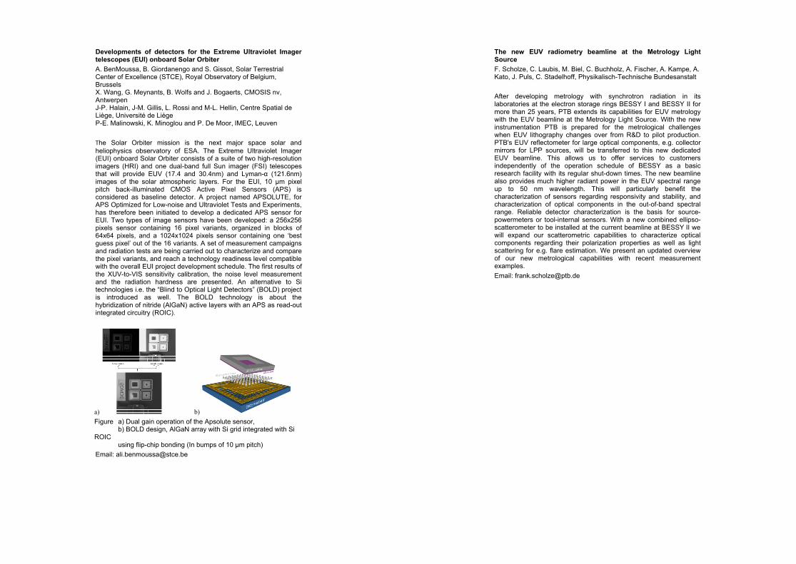
Developments of detectors for the Extreme Ultraviolet Imager telescopes (EUI) onboard Solar Orbiter A. BenMoussa, B. Giordanengo and S. Gissot, Solar Terrestrial Center of Excellence (STCE), Royal Observatory of Belgium, Brussels X. Wang, G. Meynants, B. Wolfs and J. Bogaerts, CMOSIS nv, Antwerpen J-P. Halain, J-M. Gillis, L. Rossi and M-L. Hellin, Centre Spatial de Liège, Université de Liège P-E. Malinowski, K. Minoglou and P. De Moor, IMEC, Leuven The Solar Orbiter mission is the next major space solar and heliophysics observatory of ESA. The Extreme Ultraviolet Imager (EUI) onboard Solar Orbiter consists of a suite of two high-resolution imagers (HRI) and one dual-band full Sun imager (FSI) telescopes that will provide EUV (17.4 and 30.4nm) and Lyman-α (121.6nm) images of the solar atmospheric layers. For the EUI, 10 µm pixel pitch back-illuminated CMOS Active Pixel Sensors (APS) is considered as baseline detector. A project named APSOLUTE, for APS Optimized for Low-noise and Ultraviolet Tests and Experiments, has therefore been initiated to develop a dedicated APS sensor for EUI. Two types of image sensors have been developed: a 256x256 pixels sensor containing 16 pixel variants, organized in blocks of 64x64 pixels, and a 1024x1024 pixels sensor containing one ‘best guess pixel’ out of the 16 variants. A set of measurement campaigns and radiation tests are being carried out to characterize and compare the pixel variants, and reach a technology readiness level compatible with the overall EUI project development schedule. The first results of the XUV-to-VIS sensitivity calibration, the noise level measurement and the radiation hardness are presented. An alternative to Si technologies i.e. the “Blind to Optical Light Detectors” (BOLD) project is introduced as well. The BOLD technology is about the hybridization of nitride (AlGaN) active layers with an APS as read-out integrated circuitry (ROIC).
a) b) Figure a) Dual gain operation of the Apsolute sensor, b) BOLD design, AlGaN array with Si grid integrated with Si ROIC using flip-chip bonding (In bumps of 10 µm pitch)Email: [email protected]
The new EUV radiometry beamline at the Metrology Light Source F. Scholze, C. Laubis, M. Biel, C. Buchholz, A. Fischer, A. Kampe, A. Kato, J. Puls, C. Stadelhoff, Physikalisch-Technische Bundesanstalt After developing metrology with synchrotron radiation in its laboratories at the electron storage rings BESSY I and BESSY II for more than 25 years, PTB extends its capabilities for EUV metrology with the EUV beamline at the Metrology Light Source. With the new instrumentation PTB is prepared for the metrological challenges when EUV lithography changes over from R&D to pilot production. PTB's EUV reflectometer for large optical components, e.g. collector mirrors for LPP sources, will be transferred to this new dedicated EUV beamline. This allows us to offer services to customers independently of the operation schedule of BESSY as a basic research facility with its regular shut-down times. The new beamline also provides much higher radiant power in the EUV spectral range up to 50 nm wavelength. This will particularly benefit the characterization of sensors regarding responsivity and stability, and characterization of optical components in the out-of-band spectral range. Reliable detector characterization is the basis for source-powermeters or tool-internal sensors. With a new combined ellipso-scatterometer to be installed at the current beamline at BESSY II we will expand our scatterometric capabilities to characterize optical components regarding their polarization properties as well as light scattering for e.g. flare estimation. We present an updated overview of our new metrological capabilities with recent measurement examples. Email: [email protected]
VUV and EUV scatterometry B. Bodermann, S. Bonifer, A. Kato, C. Laubis, F. Scholze, M. Wurm, Physikalisch-Technische Bundesanstalt The analysis of optical radiation scattered or diffracted at a structured surface give access to a fast and non-destructive characterisation of the structures, avoiding the constraints of imaging (microscopic) methods particularly by Abbe's diffraction limit. Thus, e. g. the widths of structures well below the optical wavelength are measurable. However, the evaluation of the measured data requires a quite complex, time- and memory-consuming mathematical treatment, the solution of the inverse diffraction problem. This in general implies periodical structures and a macroscopic interaction field. Many different methods are applied and discussed in literature, like e. g. diffractometry, reflectometry, ellipsometry and scatterometry in the actual sense, which may be summarized under the generic term "scatterometry". A short overview about the different methods and their applications will be given, including an overview of the commonly used inverse analysis methods. Some aspects concerning the potential and the limits will be discussed. Although there is no "resolution limit" in scatterometry, the application of short wavelength radiation has significant sensitivity advantages especially for the characterization of small structure details, i. e. for high spatial frequencies. Therefore, during the last years at PTB the scatterometry has been extended to the deep UV (DUV) and even to the extreme UV (EUV) spectral range. A short description of two different systems, a novel DUV hybrid scatterometer and an EUV reflectometer and scatterometer will be given. Although both systems can be used at different wavelengths they are mainly operated at wavelengths around 193 nm and 13 nm, respectively, enabling at-wavelength metrology of optical components for state of the art and future photolithography. First scatterometric measurements with these two tools of the size and shape of the cross-section profile of grating structures on a prototype EUV photomask and on a conventional 193 nm photomask will be shown and compared with each other and with electron microscopy based measurements. In general these results demonstrate the applicability both of EUV and DUV scatterometry for the characterization of different type of grating structures and show that EUV and DUV scatterometry complement each other due to their different metrological capabilities. Finally, an outlook will be given on future developments at PTB of scatterometry and ellipsometry for dimensional characterization of nanostructures. Email: [email protected]
X-ray reflectometry and small angle scattering M. Krumrey, Physikalisch-Technische Bundesanstalt X-ray reflectometry (XRR) using X-ray tubes with Cu-Kα radiation is widely used for nanolayer thickness measurements with relative uncertainties of about 1 %. By using different monochromator beamlines in the laboratory of PTB at the synchrotron radiation facility BESSY II, any X-ray wavelength from several nm down to about 0.1 nm can be selected for dimensional measurements in the nanometer range. Here, XRR is performed at wavelengths in the vicinity of an absorption edge of the chemical elements involved in order to enhance the contrast for layer systems like SiO2/Si which are difficult to resolve with Cu-Kα radiation. By using longer wavelengths of around 2 nm, even an oxide layer and a thin carbonaceous contamination layer on a strongly curved spherical surface were separated, as required for measurements at 95 mm diameter silicon spheres within the international Avogadro project for the new definition of the kilogram. For nanoparticles in suspension, small angle X-ray scattering (SAXS) is the method of choice for dimensional metrology. This ensemble technique requires intense, monochromatic X-rays of low divergence. From the scattering pattern, the particle diameter and the size distribution are obtained. Moreover, dimensional properties of nanostructured surfaces and nanoparticles on surfaces have been studied by grazing incidence SAXS (GISAXS), combining small angle scattering with the reflection geometry known from XRR. Diameters of gold nanoparticles obtained by SAXS and GISAXS are in very good agreement. Email: [email protected]
Investigation of 3D patterns on EUV masks S. Burger, L. Zschiedrich, J. Pomplun, F. Schmidt, A. Kato, C. Laubis, F. Scholze Zuse Institute Berlin, JCMwave, Physikalisch-Technische Bundesanstalt Extreme ultraviolet (EUV) lithography is expected to replace DUV photolithography for semiconductor manufacturing at the 16 nm technology node and beyond. High-throughput and high-accuracy metrology at mask and wafer level is necessary for characterization and process control. In previous works it has been shown that EUV scatterometry is a fast and robust method for characterizing lines profiles within 1D-periodic test patterns (line masks). Recently we extended our research to the characterization of 2D-periodic patterns on EUV masks (arrays of contact holes). Scatterometric measurements of these patterns have been performed using the X-ray radiometry beamline of the electron storage ring BESSY II. Rigorous simulations of the measurements have been performed using the finite-element (FEM) based Maxwell solver JCMsuite. We present experimental results and simulation results with very good agreement, allowing for parameter reconstruction. Email: [email protected]
On Born approximation for the scattering by rough surfaces T. Arnold and A. Rathsfeld, Weierstrass Institute for Applied Analysis and Stochastics, Leibniz Institute in Forschungsverbund Berlin e.V. For scatterometric measurements of EUV-lithography masks, due to short wavelengths and tiny dimensions in the mask geometries, the various impacts of roughness cannot be neglected anymore. In particular, the roughness of the interfaces in the multi-layer systems serving as mirrors can essentially affect the accuracy of the measurements. Consequently, the scattering by rough surfaces and interfaces must be analyzed. Unfortunately, mathematically strict variational models for the Maxwell system do not, yet, cover the incidence of plane waves onto rough surfaces. Therefore simplified models are of great importance, for both the analysis and the fast numerical solution. Note that, at the beginning of such an analysis, the rough surface is simply the graph of a smooth, bounded, and aperiodic function. One way to provide a simplified model is proposed by Stearns [1] and is based on the Born approximation, i.e. on the neglect of lower order terms in the Maxwell’s equations. The new equations can easily be resolved by Fourier transform methods. We will discuss mathematically strict assumptions which justify the manipulations in Stern’s approach. Under these assumptions, we will present rigorous formulas of Maxwell solutions approximating the fields scattered by the rough surface. Finally, we derive the corresponding formulas for the scattered far field. [1] D.G. Stearns, The scattering of x rays from nonideal multilayer structures, J. Appl. Physics 65 (2), 1989, pp. 491-506 Email: [email protected]
Model based uncertainty estimations for inverse scatterometry H. Gross, M. A. Henn, A. Rathsfeld* and M. Bär, Physikalisch-Technische Bundesanstalt, *Weierstrass Institute for Applied Analysis and Stochastics Impacts of model based uncertainties and sensitivity analysis for the determination of periodic surface structures from light diffraction patterns are discussed. With decreasing feature sizes of lithography masks, increasing demands on metrology techniques arise. Scatterometry as a non-imaging indirect optical method in wafer metrology is applied to periodic line structures in order to determine critical parameters like side-wall angles, heights, top and bottom widths and to estimate their associated uncertainties. In 2D, the numerical simulation of light diffraction can be realized by the finite element solution of the Helmholtz equation. The inverse problem seeks to reconstruct the surface geometry from measured diffraction patterns. Restricting the class of surface structures and the set of measurements, this inverse problem can be reformulated as a non-linear operator equation in Euclidean spaces. The operator maps the grating parameters to diffraction efficiencies or phase shifts of diffracted plane wave modes. Different iterative methods to solve this operator equation can be applied. We employ the Gauß-Newton method, i.e. we minimize the deviation of the measured data values from the calculated ones. Furthermore we employ a maximum likelihood estimation (MLE) to get access to the uncertainties of the measurement values. Clearly, the uncertainties of the reconstructed profile parameters depend on the uncertainties of the all input data and can be estimated by various methods like Monte Carlo or covariance methods, provided the latter uncertainties are known. Unfortunately, the mathematical model for the surface profile is only an approximation. Due to the large number of parameters it takes to simulate a realistic mask, some of them have been fixed in the mathematical model. Therefore, a priori knowledge about reasonable values for certain model parameters and the associated variances is needed and their impact on the reconstructed profile parameters has to be considered too. Furthermore, there are assumptions which are inherent properties of the direct model, namely that the structures are periodic over a sufficiently large area. Effects like line roughness disturbe the periodicity of the surface structure and the corresponding uncertainty contribution can become crucial. To evaluate the reconstruction algorithm under these aspects, numerical examples for extreme ultraviolet (EUV) masks irradiated with light of wavelength in the range of 13.5 nm are presented. Email: [email protected]
EUV optics for Free Electron Lasers S. Bajt, Photon Science, DESY, Hamburg Free Electron Lasers provide high intensity, coherent, femtosecond x-ray pulses. They are new tools for investigating ultrafast dynamic properties at atomic resolution. These novel x-ray sources offer new opportunities but also challenges for x-ray optical elements. At our newly established X-ray multilayer laboratory at DESY in Hamburg we are developing and fabricating multilayer-based optical elements for FEL experiments. Soft x-ray reflectometry measurements are essential to test high precision multilayer-based optics for their performance at a desired wavelength. As compared to optics used with other x-ray sources such as synchrotrons, this characterization is more critical than ever. Getting FEL beamtime is a highly competitive process and its efficient use is essential for the success of the experiment. In addition, standard alignment techniques that can be safely used with synchrotron light pose damage or even destruction to the optic exposed to the direct FEL beam. In this talk we will present few examples of x-ray optics that were used to focus, reflect and/or filter the FEL beam in different FEL experiments. Some examples, characterized at PTB beamline before and after FEL experiments, will be discussed as well. Email: [email protected]
Sputter technologies for the development of EUV and X-Ray mirrorsS. Braun, IWS Dresden, Fraunhofer Institute for material and beam technology Abstract Multilayer mirrors with high reflectance and/or good energy resolution for X-ray and EUV optical applications need both smooth interfaces and sharp transitions between the adjacent layers of the absorber and spacer materials. Sputter techniques like magnetron sputter deposition (MSD) and ion beam sputter deposition (IBSD) are promising methods for the production of high performance multilayer stacks. However, the steadily increasing requirements on run-to-run reproducibility, long-term stability and lateral uniformity of the coatings are still critical issues. In our presentation we will show the current status of sputter technologies for the deposition of EUV reflection coatings and we will show how the technology can perspectively be scaled up to larger substrate dimensions. Email: [email protected]
Development of EUV/X-Ray multilayer optics in IOF S. Yulin, V. Nesterenko, T. Feigl, N. Kaiser Fraunhofer-Institut für Angewandte Optik und Feinmechanik A demand to enhance the optical resolution, to observe ever smaller details, has pushed the search for technological innovations and improvements. Induced mainly by the production of more powerful electronic circuits with the aid of projection lithography, optics development in recent years can be characterized by the use of electromagnetic radiation with smaller wavelength. The good prospects of EUV and soft X-rays to be applied to next generation lithography systems ( = 13.5 nm), microscopy in the “water window“ ( = 2.3 - 4.4 nm), study of high-order harmonic generation (10 - 30 nm), astronomy and spectroscopy ( = 5 - 80 nm), plasma diagnostics and EUV/X-ray laser research have led to considerable progress in the optics development for this spectral range. At the Fraunhofer IOF Jena multilayer optics development cover the full spectral range from 1.0 nm to vacuum ultraviolet around 200 nm. This paper covers some theoretical considerations, material aspects, modern interface-engineered designs and techniques for controlled fabrication of Mo/Si (and La/B4C) multilayers for EUV lithography related applications, Mo/Si multilayers for high-order harmonic generation in the 20 … 30 nm spectral range, Cr/Sc and Cr/V multilayers for the water window and Sc/Si multilayers for the 42 to 50 nm wavelength range. The paper summarizes recent progress and the present knowledge in preparation and characterization of high-reflective multilayer optics for the VUV and soft X-ray range with regard to different narrowband and broadband designs, minimization of structure imperfections, enhanced thermal and radiation stability. Email: [email protected]
Multilayer coating for EUV collector mirrors M. Perske, H. Pauer, S. Yulin, M. Trost, S. Schröder, A. Duparré, T. Feigl, N. Kaiser, A. Tünnermann, Fraunhofer-Institut für Angewandte Optik und Feinmechanik Bringing EUV Lithography forward to high volume manufacturing, one of the main challenges to date is to deliver a high level of EUV power at intermediate focus. One of the most promising methods to meet the joint requirements of all leading scanner manufacturers is a high power laser produced plasma source. Ellipsoidal collector mirrors for Extreme Ultra Violet Lithography (EUVL) have to be coated with a highly reflective, laterally graded multilayer to achieve a consistently high reflectance of more than 65 % at a wavelength of (13.50 ± 0.03) nm over the entire surface. The multilayer deposition of those collectors with a diameter of 660 mm still poses one of the biggest challenges with respect to the extreme demands on quality, accuracy and lifetime. Before coating, the collector surface finish has to be characterized in terms of high spatial frequency roughness in order to verify the specified surface roughness of less than 0.2 nm (rms). In combination with multilayer scattering theories, the optical properties of the multilayer stack also allow a prediction of the possible reflectance. For these measurements a novel 3-D Arrangement for Laser BAsed Transmittance, Reflectance, and Optical Scatter MeaSurement (ALBATROSS) has been developed at Fraunhofer IOF. This paper presents technical advances in surface characterization methods by ALBATROSS and latest coating results of 5 sr collector mirrors for EUVL deposited by DC magnetron sputtering. Email: [email protected] Multilayer development for next generation EUVL optics E. Louis1, S. Müllender2, and F. Bijkerk1,3
1FOM Rijnhuizen, Nieuwegein, 2Carl Zeiss SMT AG, Oberkochen, 3 MESA+ Institute for Nano Technology, University of Twente
Multilayer coatings form a key component of EUV optical systems. The research required to develop this class of optics is ongoing for several decades already. In this presentation we will discuss the path from fundamental research on the deposition of layers of a few nm thickness only towards a fully developed process, matured to deposit optics for prototype lithography machines. Topics like multilayer deposition, smoothing of interfaces, thermal stability, interface engineering, multilayer induced stress, and lateral uniformity will be discussed and examples of multilayer coated optics that fulfill the extremely tight specifications of EUV lithography machines will be given. Furthermore, solutions to suppress parasitic longer wavelength radiation emitted by EUV sources will be discussed. Yet, while the first EUV litho tools are being shipped to semiconductor manufacturers, research on multilayers for an even shorter wavelength of 6.x nm already takes place. This means other multilayer materials and, because of its increasing importance, even more focus on issues like smooth layer growth and prevention of intermixing. Email: [email protected]
Laser based plasma sources for EUV and XUV H. Stiel2, I. Mantouvalou1,2, G. Blobel2, R. Jung2, B. Kanngießer1, H. Legall2 , J. Tümmler2, K. Witte1 1Technical University of Berlin, 2Max-Born-Institute, Berlin Laboratory for innovative X-ray technologies (BLiX) For applications in soft x-ray spectroscopy, nano-scale imaging or extreme ultraviolet (EUV) metrology there are two basic source requirements: a high spectral brightness and a high average photon flux. A high coherence is required for applications in interferometry or holography. Laser based plasma (LPP) sources are well suited as soft x-ray sources for applications described above. However, to meet both demands high brightness and high average power dedicated optimized pump laser systems are required. We present here novel compact, high average power, high spectral brightness soft xray sources based on a high repetition rate thin disk laser pump system. The first source is a plasma based x-ray laser (XRL) emitting highly monochromatic coherent EUV radiation with high peak brightness. In the second part of the talk we will discuss the performance of thin disk laser pumped plasma sources emitting incoherent soft xray radiation between 100 eV and 1200 eV. We will discuss two different LPP setups built at BLiX. Email: [email protected]
Metrology applications of XUV laboratory sources L. Juschkin, University College Dublin The use of extreme ultraviolet and soft x-ray radiation enables a variety of new optical, analytical and production procedures. Taking into account the recent progress in the development of sources and optics, XUV applications in semiconductor industry, thin-film technology, life- and material sciences are envisioned. Examples are the determination of element composition, layer thickness and surface roughness from grazing incidence reflectivity, defect identification from scattered light measurements for e.g. mask-blank inspection using EUV microscopy, and lithography to produce periodic nanostructures with high throughput. Many applications, like mapping of mask blanks for EUV lithography, require the ability to scan large surfaces for the presence of small printable defects on a nanometer scale as rapidly as possible. The distinct features of XUV light such as the short wavelength allowing for nanometer resolutions and its strong interaction with matter resulting in high elemental contrast and photochemical sensitivity make it a promising candidate for future metrology systems. Additionally time-resolved microscopy utilizing EUV light can be deployed for the investigation of dynamic behaviors of nanostructures. The talk presents the work of the EUV-Technology group at the Chair for Technology of Optical Systems at the RWTH Aachen University in the field of laboratory scaled XUV applications. E-mail: [email protected]
EUV mask reflectometer R. Lebert, A. Farahzadi, U. Wiesemann, W. Diete, Bruker Advanced Supercon GmbH There is a strong demand for standalone actinic tools for mask blank and mask metrology. We expect to deliver contributions to key issues for the infrastructure tools such as actinic reflectometer, actinic defect inspection and components like high brightness sources together with our partners. Transferring metrology from high brilliance synchrotron sources to isotropic, line emitting discharge sources is most efficient, by adapting the scheme of measurement. Applying our "polychromatic scheme" for an EUV-reflectometer developed for mask blank characterization (EUV-MBR), precision of 0.1 % in peak reflectivity and < 0.002 nm for centroid wavelengths (1 sigma) are routinely achieved on both reflective multilayer coated and absorber coated blanks with < 20 s exposure on a 100x100 µm² spot. These values are close to requirements for High volume manufacturing (HVM) of EUV-masks and is accomplished along with fully automated operation (loading, alignment and positioning) and the ability for referencing to fiducial marks and measuring on structured sites of a mask. It has been demonstrated that our discharge based "EUV-Lamp" enables EUV-MBR operation without wear or components change for > 300 million pulses, which is > 100.000 full (2000 wavelength cannels) spectra measured at different sites or > 10.000 samples measured at 9 spots and thus meets uptime demands in the > 95 % range. Email: [email protected] In-house EUV reflectometry at Carl Zeiss SMT T. Böttger, Carl Zeiss SMT Recently, a new EUV reflectometer (EUVR2), based on the research and experience on the prior laboratory reflectometer (EUVR1), has been developed for characterization of next product generation EUV mirrors at Carl Zeiss SMT. The EUVR2 is a useful part in at-wavelength metrology for coating development and production, and is capable to meet the requirements in multilayer mirror quality assurance for reflectivity, layer thickness control, and coating uniformity. It consists of a laser-produced plasma radiation source, a high resolution monochromator and a lubricant free goniometer system. The EUVR2 can handle aspherical mirrors with max. 750 mm diameter, 300 mm thickness and up to 50 kg weight. The wavelength can be varied from 10 nm to 18 nm with a spectral resolution > 750 λ/Δλ. The standard spot size on the mirror surface is Ø 0.5 mm. The incidence angle can be varied from 1° to 90° . The measured multilayer peak reflectivity and center wavelength can reproduced within 0.035% and 0.15 pm, respectively. Email: [email protected]
Posters Realization of extreme ultraviolet phase transmission gratings made from diamond filmsC. Braig, Friedrich-Schiller-Universität Jena We present experimental results on the development of true free-standing phase transmission gratings for the soft X-ray and extreme ultraviolet band. An ultra-nanocrystalline, 300 nm thin diamond film on a backside etched silicon wafer is precisely structured via electron-beam lithography to periods of 1 µm. In this way, flat and stable circular gratings of 400 µm in diameter are fabricated. Symmetric first-order net efficiencies up to 28% are obtained from measurements at the PTB synchrotron beamline within a wavelength range from 5.0 nm to 8.3 nm, whereas the 0th order is well suppressed to 1% near 6.8 nm. Higher diffraction orders up to the 3rd one contribute less than 7% in sum to the far-field pattern. Moreover, the data indicate an extraordinary high EUV quality of the chemical vapor deposited diamond film in use, in terms of its complex refractive index. Email: [email protected]
Time resolved EUV pump-probe microscopy of fs-laser induced nanostructure formation R. Freiberger, Technology of Optical Systems, RWTH Aachen We report on our efforts on setting up and building a compact extreme ultraviolet (EUV)-pump-probe microscope. Our goal is the observation of femtosecond (fs)-laser induced nanostructure formation. The unique interaction processes induced by fs-laser radiation open up new markets in laser material processing and are therefore matter of actual research. "Sub 100 nm"-structures offer vast potential benefits in photonics, biotechnology, tribological surface design, plasmonic applications and production of nanoparticles. Focused fs-laser radiation causes a local modification resulting in nanostructures of high precision and reproducibility. However the formation dynamic is not well understood. Research in this field requires high temporal and spatial resolution. A combination of fs-laser and EUV-microscope provides a tool for "in situ"-observation of the formation dynamics. As exemplary structures to be investigated, we use nanojets on thin gold films and periodic surface structures (ripples) on dielectrics. The gateable MCP detector provides a necessary time resolution (< 2ns) and, together with the high magnification zone plate, will allow the constructed EUV-pump-probe microscope to observe physical or biological processes with high spatial and temporal resolution. Email: [email protected]
Characterization of a microchannel plate imaging EUV-detector with 2 ns temporal resolution J. Hauck, Technology of Optical Systems, RWTH Aachen Research in nanoscale dynamics requires high spatial and temporal resolution detectors. We show a detector which is capable of taking photos in the EUV with 2 ns shutter time and a spatial resolution of 83 µm. It consists of a microchannel-plate photoelectron multiplier together with a phosphor screen and a CCD camera for readout. The pulsed operation voltage of the electron-multiplier gives a narrow temporal sensitivity window. The following attributes of the detector system were analyzed:
Temporal behavior is measured by femtosecond illumination with HHG radiation at different relative delays. The sensitivity curve has a width of 2 ns. Electronic timing jitter is below 150 ps.
Spatial resolution is determined by mapping a sharp shadow on the detector. Structures with a minimum pitch of 80 µm can be resolved.
Spectral sensitivity of the detector is calibrated at the PTB EUV facility at the BESSY II synchrotron. The peak sensitivity is reached between 9 nm and 15 nm wavelength.
The detector is used in a zone plate based DPP-EUV microscope which provides a spatial resolution down to 80 nm and a time resolution of 2 ns. This highly interesting combination will help to investigate a variety of short time processes in nanoscience. Email: [email protected]
EUV imaging of nanoscale defects S. Herbert, RWTH Aachen Here we present the current research in the field of nanoscale defect inspection. A proof of principle setup based on a dark-field EUV microscope has been designed and constructed. The tabletop setup consists of a gas discharge plasma source, a grazing incidence collector, a deflection mirror, a five axis sample holder, a Schwarzschild objective and a back-thinned and backside illuminated CCD camera. For characterization measurements of the setup, several test structures have been fabricated. On a multilayer mirror bump structures have been deployed and pit structures have been drilled with a focused ion beam into a multilayer mirror. These structures have been investigated with an Atomic Force Microscope for cross correlation of the results. Furthermore a simulation model of defect scattering has been developed, which is based on the diffraction of a pinhole. A comparison of experimental and simulation results will be presented. System limitations (due to detectors-, mechanics- or optics- performance) have been analyzed and will be shown. To expand the detector limitation, an alternative detector concept has been developed. Experimental results on EUV quantum efficiency of the detector will be shown. Email: [email protected]
Metrology oriented activity at BEAR N. Mahne1, A. Giglia1, S. Mukherjee2, S. Nannarone1,3 1IOM - CNR Laboratorio TASC, Trieste, 2Abdus Salam International Centre for Theoretical Physics, Trieste, 3Università di Modena e Reggio Emilia, Modena BEAR (Bending magnet for Emission Absorption and Reflectivity) is a beamline at Elettra (Trieste, Italy); its mission includes aspects ranging from basic research in field of ultra-thin films and interfaces to metrology of materials and optical devices. The apparatus works in the visible-soft-x region (3-1800 eV) with linear (S, P) or elliptical polarization and allows monitoring of beam stability and spectral purity (<1%), with a spot of 30×400 µm2 (typical) and 20mrad divergence. High degree of flexibility of the endstation permits changing of incidence angle from 0° (normal) to ~89° (grazing), and angle-resolved measurements. Samples can be prepared (cleaning, annealing, deposition, etc.) in a separate chamber. Installed measurement techniques include reflectivity, specular (energy, θ-2θ scan) and diffused (rocking, detector scan), transmittance, XMCD, fluorescence and XEOL measurements. Optical characterization can be assisted by surface science techniques: photoemission, Auger spectroscopy. A number of examples of metrology oriented studies are presented: optical constants of rare earths, mirror reflectivity, analysis of buried interfaces using standing-wave assisted photoemission and luminescence, roughness determination by diffused reflectivity, optical characterization of wide-band ML for ultra-fast spectroscopy in UV, characterization of laser damaged ML, UV filter for space applications, magnetic multilayers. Future plans include development of UV polarimetry by SR, measure UV piezo-dichroism of crystals, UV chiral absorption by proteins. A code (OPAL) is under development for simulation of optical response of anisotropic and/or magnetized media. Email: [email protected]
Diagnostics and brilliance improvement of EUV radiation at FEL FLASH and labscale sources T. Mey, Laser-Laboratorium Göttingen e.V. Hartmann sensors and caustic scans are standard tools to assess and improve beam and imaging quality over a wide range of wavelengths, including EUV and soft x-rays. A Hartmann sensor was developed within a collaboration between the Laser-Laboratorium Göttingen e.V. and HASYLAB for applications in the soft x-ray regime. The sensor was used for beam parameter determination and mirror alignment at beam lines BL1 and BL2 at FLASH, accomplishing an improved focusability of the FEL beam. However, Hartmann and caustic techniques provide no or little information on the coherence properties of the beam. Here we propose a Wigner decomposition, gained by a caustic scan of the FLASH beam, providing the global degree of coherence. Additionally, we present the latest improvements of our laser driven lab scale EUV/XUV plasma source which utilizes gases as target material. Operating such sources, the aim is to achieve preferably high mass densities of the target to attain a hot and dense plasma, i.e. a high quantum conversion efficiency. Provoking a supersonic shock in the gas jet, we locally increase the mass density leading to a smaller and brighter plasma. Email: [email protected]
The DESIRS beamline VUV Fourier Transform Spectrometer: a unique instrument for ultra-high resolution absorption spectroscopy N. de Oliveira, D. Joyeux , M. Roudjane and L. Nahon, Société Civile Synchrotron Soleil
Since 2008, the Fourier transform spectrometer (FTS) is in operation at SOLEIL on a dedicated branch of the VUV beamline DESIRS. This instrument has been developed in order to cover specifically the VUV range [8-30 eV]. So far, such a FT technique was totally absent in that range due to the difficulty in manufacturing one of the interferometer main optical component: the beamsplitter. This problem has been overcome by using a wave front division interferometer instead of the traditional wave amplitude division scheme [1]. The experiments performed on the DESIRS beamline gave unprecedented results in terms of the resolving power (close to 106) over a broad VUV spectral range, together with a high absolute spectral accuracy and a high efficiency in terms of signal to noise ratio as compared with scanning spectrometers, due to the multiplex spectral acquisition of FT spectroscopy [2]. An overview of the present and potentially future scientific application program, mainly centered on the study of small molecular systems of astrophysical interest, will be shown.References [1] N. de Oliveira et al., Rev. Sci. Instrum. 80, 043101 (2009) [2] N. de Oliveira et al., Nature Photonics 5, 149–153 (2011) Email: [email protected]
Development of super mirrors for first X-ray LMJ microscopes R. Rosch, CEA Bruyères le Châtel The Laser Mégajoule (LMJ) facility, now under construction at CEA/CESTA, will be with the National Ignition Facility (NIF) one of the world’s largest laser driven fusion facilities in operation in the 2010’s. We present here the design of the first set of diagnostics to be implemented on LMJ. This set includes three imaging diagnostics with high spatial, temporal and spectral resolution. They will give basic measurements, during all the life of the facility, such as position, structure and balance of beams, but they will also be used to diagnose implosions in indirect drive. Thus, the design requires a vulnerability approach, because components will operate in a harsh environment induced by fluxes of neutrons, gamma rays, debris and shrapnel. Grazing incidence X-ray microscopes as far as possible from the target are a good way to mitigate this environment. All microscopes include toroidal mirrors and reflect x-rays up to 10 keV using W/SiC non-periodic multilayer coatings (Super mirrors) developed in collaboration with the LCFIO. The mirrors were designed and optimized with TFCALC code. Supermirrors are dedicated to work at 0.7° grazing incidence. Metrology at synchrotron radiation facility BESSY II is presented. Email: [email protected]
MicroSys2000: Deposition of EUV reflection coatings on large area substrates D. Rost1, S. Braun2, M. Nestler1, P. Gawlitza2, M. Menzel2, M. Zeuner1 1Roth & Rau MicroSystems GmbH, Hohenstein-Ernstthal, 2Fraunhofer Institute for Material and Beam Technology (IWS), Dresden Magnetron Sputter Deposition (MSD) has been established as a coating technology for the production of EUV reflection optics. EUV reflection coatings consist of nanometer multilayers which have to fulfill demanding requirements with respect to reflectance, uniformity, reproducibility and low residual stress. Using MSD all the tight specifications can be met at the same time on large substrates. With our poster we will present a typical MSD coating machine called MicroSys2000 and the corresponding multilayer properties. The MicroSys2000 can be used for multilayer depositions on optics with diameters of up to 670 mm. The process chamber of the machine contains six planar sputter magnetrons used for the subsequent deposition of up to six different materials. The sputter sources are arranged radial-symmetrically in a hexagonal chamber. The main rotation around the center of the process chamber moves the substrates over the targets. By altering the velocity of the movement the layer thickness can be precisely controlled. Additionally, the substrate spins around its axis in order to improve the lateral uniformity of the coatings. With optimized processes excellent values for reflectance, uniformity and run-to-run reproducibility can be achieved using MicroSys2000. Email: [email protected]
Desk-top actinic imaging with nanometer spatial resolution P. Wachulak, A. Bartnik, H. Fiedorowicz, R. Jarocki, J. Kostecki, A. Szczurek, M. Szczurek, Military University of Technology, Warsaw The wavelengths in the EUV range make possible to see smaller structures and write smaller patterns. It is expected that EUV lithography (EUVL), with the use of radiation at the 13.5nm wavelength, will enable a mass production of electronic chips at the 22nm node and beyond; however, there are still several serious problems to be solved, including optics degradation, source development, photoresist resolution, and mask defects. Further improvement in defect reduction will come as actinic inspection tools (aerial image measurement system and full blank inspection) become commercially available. The lack of these compact and widely available tools is one of leading challenges for EUVL. In the paper we present the first experiments on actinic EUV imaging with nanometer resolution using a compact laser plasma source and Fresnel zone plate optic. The images of a various objects were registered with a EUV sensitive CCD camera. Using a well-established “knife-edge” tests the spatial resolution (half-pitch) of 51nm was obtained. It is the first demonstration of nanoscale actinic EUV imaging using a compact, desk-top device. Experiments on nanoimaging at shorter wavelengths of EUV and soft X-rays are under preparation. Email: [email protected]
Physikalisch-Technische BundesanstaltInstitut Berlin
Sponsored by: