euv lithography insertion - semicontaiwan.org · euv lithography insertion semicon taiwan taipei...
TRANSCRIPT

Kars Troost, PhD Senior Product Manager EUV
final
EUV Lithography
Insertion
Semicon TaiwanTaipei
Sept 3rd, 2015
Public
• EUV Insertion focus
• EUV Benefits
• Field performance
• Productivity
• Imaging, Overlay, Defectivity
• Infrastructure status
• Summary
AgendaSlide 2
Public
Slide 3
PublicEUV insertion is focusing on the 7nm node
• EUV insertion is currently focusing on the 7nm node
• Production 2018, production system shipments 2017
• Insertion will be determined by the production readiness of EUV versus
the complexity of multiple patterning
• EUV initially will replace the most difficult multiple patterning layers
• Other layers will remain allocated to immersion for the foreseeable future
• DUV and EUV will be available in parallel for many years to come
• ASML remains committed to advancing both technologies to provide the
mix that best meets customers’ performance and cost requirements
Slide 4
Public
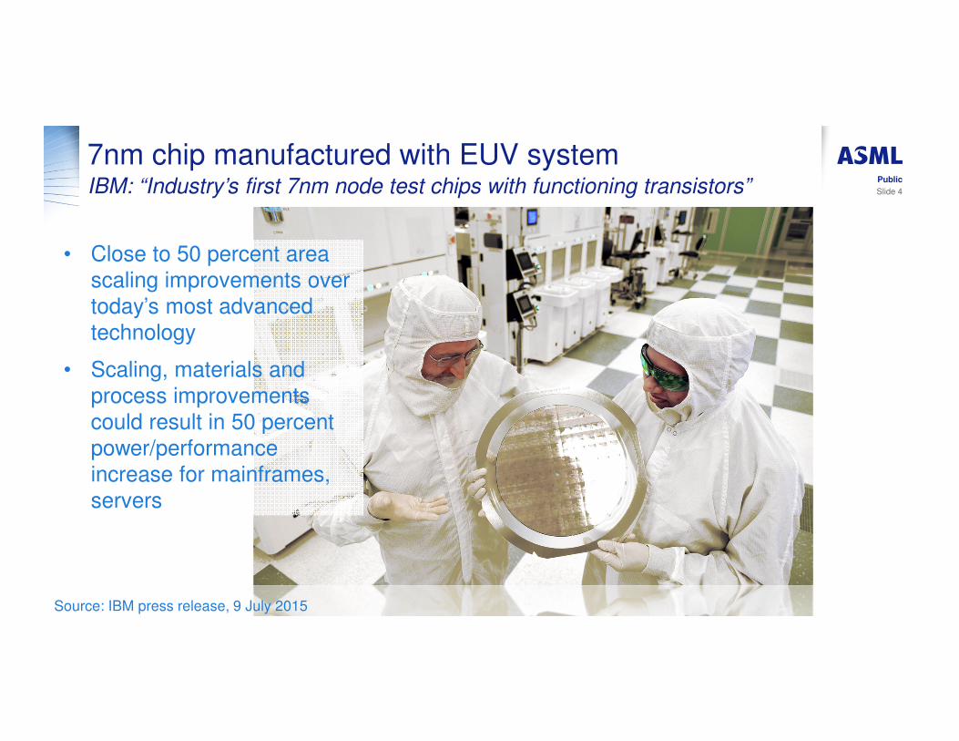
7nm chip manufactured with EUV systemIBM: “Industry’s first 7nm node test chips with functioning transistors”
• Close to 50 percent area
scaling improvements over
today’s most advanced
technology
• Scaling, materials and
process improvements
could result in 50 percent
power/performance
increase for mainframes,
servers
Source: IBM press release, 9 July 2015
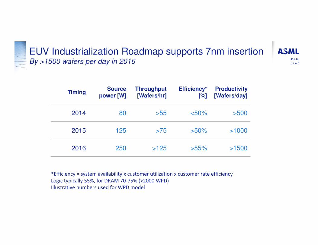
EUV Industrialization Roadmap supports 7nm insertion By >1500 wafers per day in 2016
TimingSource
power [W]Throughput [Wafers/hr]
Efficiency*[%]
Productivity [Wafers/day]
2014 80 >55 <50% >500
2015 125 >75 >50% >1000
2016 250 >125 >55% >1500
*Efficiency = system availability x customer utilization x customer rate efficiency
Logic typically 55%, for DRAM 70-75% (>2000 WPD)
Illustrative numbers used for WPD model
Public
Slide 5

Slide 6
Public
EUV reduces complexity and thus cycle time20 n
m (
Imm
ers
ion)
8xMasks
10 n
m (
Imm
ers
ion)
23xMasks7 n
m(I
mm
ers
ion)
33xMasks
7n
m(E
UV
)
9xMasks
Node # of litho steps
# OVL Metrology
# max metrology /
litho steps
20 nm
8 (Immersion)
9-11
2
10 nm23 (Immersion)
36-40
3
7 nm33 (Immersion)
59-65
4
7 nm
12
3
Layers
9 (EUV)
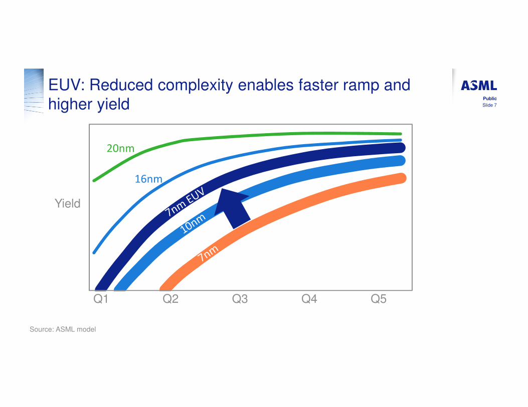
EUV: Reduced complexity enables faster ramp and
higher yield
20nm
16nm
Q1 Q2 Q3 Q4 Q5
Yield
Source: ASML model
Public
Slide 7
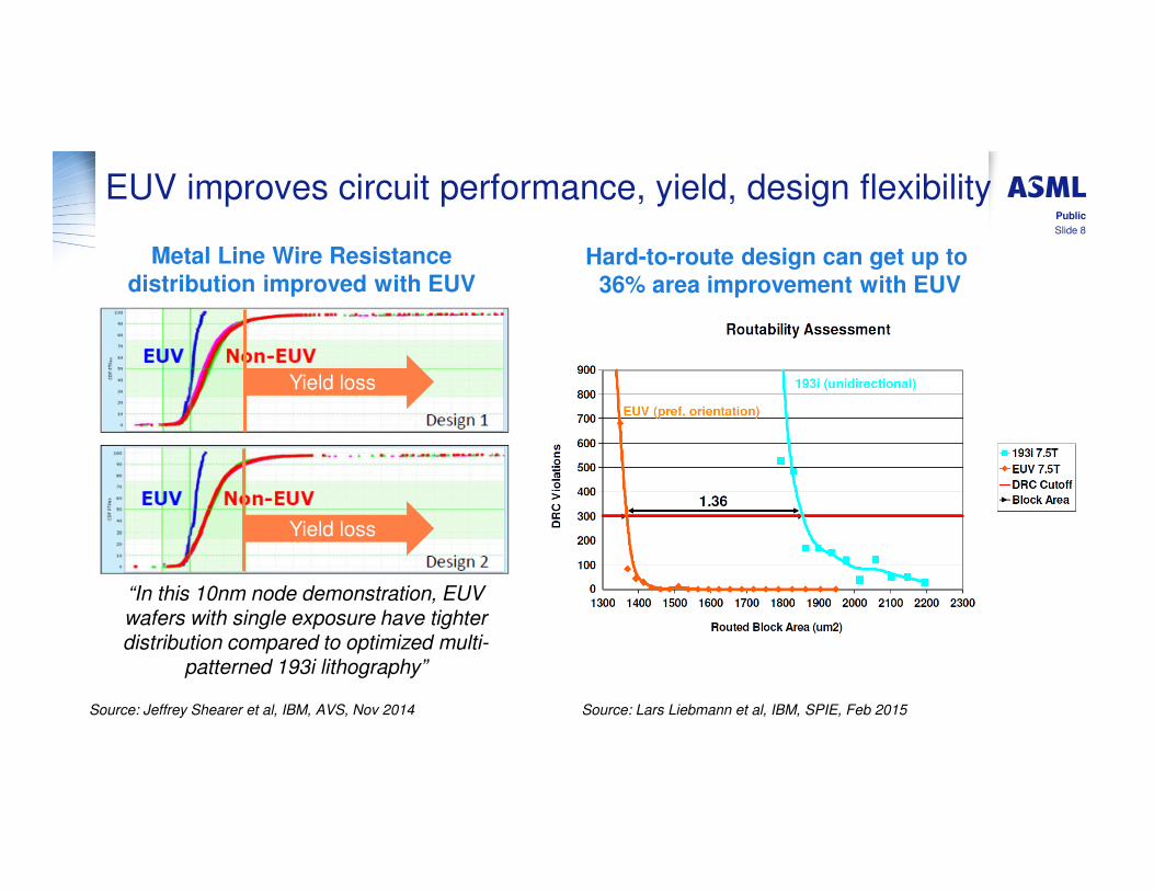
EUV improves circuit performance, yield, design flexibility
“In this 10nm node demonstration, EUV wafers with single exposure have tighter distribution compared to optimized multi-
patterned 193i lithography”
Metal Line Wire Resistance
distribution improved with EUV
Yield loss
Yield loss
Slide 8
Public
Source: Jeffrey Shearer et al, IBM, AVS, Nov 2014 Source: Lars Liebmann et al, IBM, SPIE, Feb 2015
Hard-to-route design can get up to
36% area improvement with EUV

Slide 9
Public
Moore’s Law cost reduction stays on track with EUVMultiple patterning costs reduced
Source: ASML, IC Knowledge, IMEC
Validated with external consultants
NoN = Node on NodeYoY = Year on Year
÷>40% NoN
reduction
>40% NoN
reduction
2014
2015
2004 2006 2008 2010 2012 2014 2016 2018 2020
Rela
tive C
ost per
Function
1%
10%
100%
2002 2004 2006 2008 2010 2012 2014 2016 2018 2020 2022
Total
Litho
Other patterning
TotalLithoOther
2002 2004 2006 2008 2010 2012 2014 2016 2018 2020 2022
100%
10%
1%Rela
tive C
ost per
Wafe
r
Total cost
Litho cost
Other patterning cost
10
100
2012 2013 2014 2015 2016 2017 2018 2019 2020 2021 2022
Max
. Tra
nsi
sto
r d
ensi
ty [
#/m
m^2
]
Year of HVM
Transistor density
[M#]
2012 2013 2014 2015 2016 2017 2018 2019 2020 2021 2022
Transistor density [M#]
10
100
Max. T
ran
sis
tor
den
sit
y [
#/m
m^
2]
Tra
nsis
tors
per
mm
2
>45% YoY
increase
>45% YoY
increase
g
Slide 10
Public
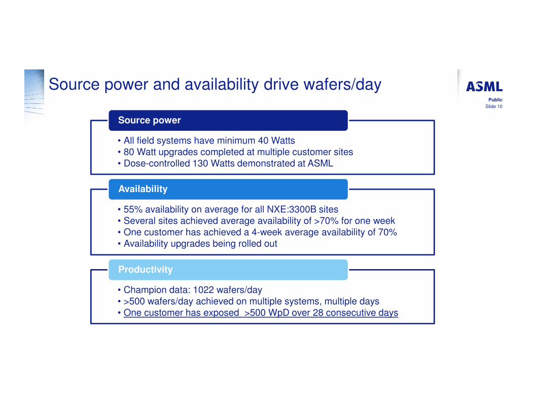
Source power and availability drive wafers/day
• All field systems have minimum 40 Watts
• 80 Watt upgrades completed at multiple customer sites
• Dose-controlled 130 Watts demonstrated at ASML
Source power
• 55% availability on average for all NXE:3300B sites
• Several sites achieved average availability of >70% for one week
• One customer has achieved a 4-week average availability of 70%
• Availability upgrades being rolled out
Availability
• Champion data: 1022 wafers/day
• >500 wafers/day achieved on multiple systems, multiple days
• One customer has exposed >500 WpD over 28 consecutive days
Productivity

Slide 11
Public
EUV power scaling: three leversCO2 power, conversion efficiency, EUV energy available for exposure
10 W
Increase
CO2 power
Increase
conversion
efficiency
Lower
dose
overhead
250 W
NXE:3100(“NOMO”)
NXE:33x0B(“MOPA-Pre-Pulse”)

15 April 2015
Slide 12
Public
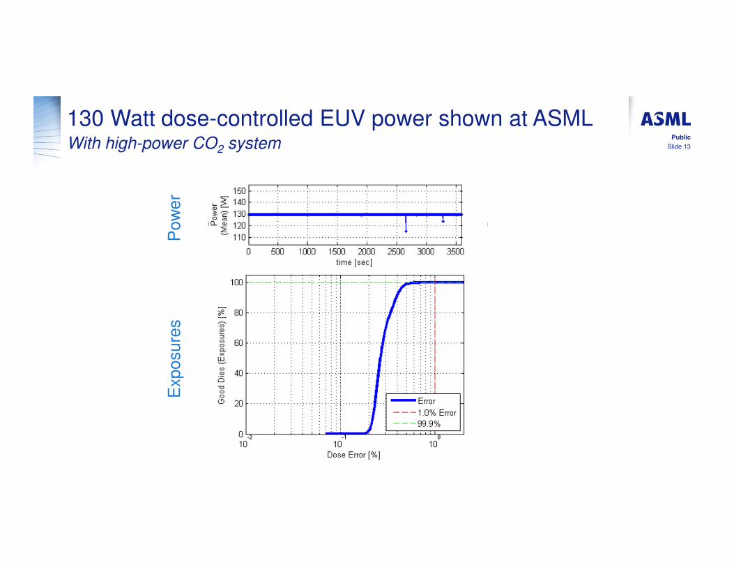
130 Watt dose-controlled EUV power shown at ASMLWith high-power CO2 system
Public
Exposure
sP
ow
er
Slide 13
Slide 14
Public
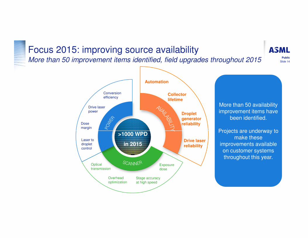
Focus 2015: improving source availabilityMore than 50 improvement items identified, field upgrades throughout 2015
Conversion
efficiency
Dose
margin
Drive laser
power
Laser to
droplet
control
Optical
transmission
Overhead
optimization
Exposure
dose
Stage accuracy
at high speed
>1000 WPD
in 2015
Automation
Collector lifetime
Droplet generator reliability
Drive laser reliability
More than 50 availability improvement items have
been identified.
Projects are underway to make these
improvements available on customer systems throughout this year.
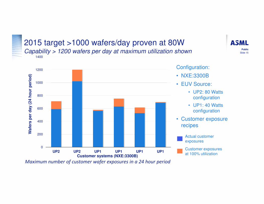
2015 target >1000 wafers/day proven at 80W Capability > 1200 wafers per day at maximum utilization shown
0
200
400
600
800
1000
1200
1400
UP2 UP2 UP1 UP1 UP1 UP1
Configuration:
• NXE:3300B
• EUV Source:
• UP2: 80 Watts configuration
• UP1: 40 Watts configuration
• Customer exposure
recipes
Actual customer
exposures
Customer exposures
at 100% utilization
Wa
fers
pe
r d
ay (
24
ho
ur
pe
rio
d)
Maximum number of customer wafer exposures in a 24 hour period
Customer systems (NXE:3300B)
Public
Slide 15

Public
Slide 16
> 500WPD in 4 consecutive weeks proven at customer Automated reticle & wafer loading. Imaging & overlay in specification
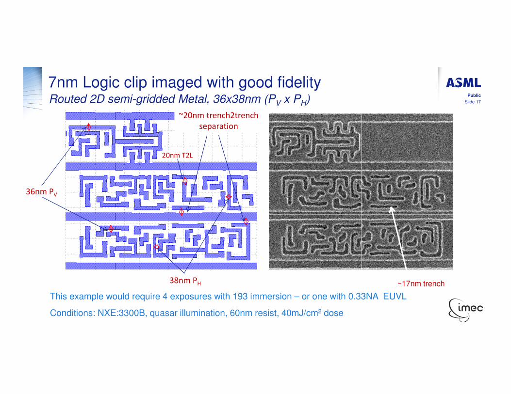
7nm Logic clip imaged with good fidelityRouted 2D semi-gridded Metal, 36x38nm (PV x PH)
36nm PV
~20nm trench2trench
separation
38nm PH
20nm T2L
~17nm trench
This example would require 4 exposures with 193 immersion – or one with 0.33NA EUVL
Conditions: NXE:3300B, quasar illumination, 60nm resist, 40mJ/cm2 dose
Public
Slide 17
Slide 18
Public
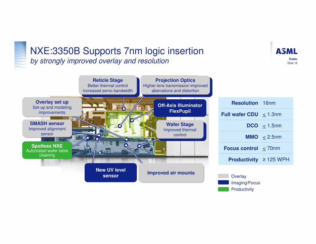
NXE:3350B Supports 7nm logic insertionby strongly improved overlay and resolution
Resolution 16nm
Full wafer CDU < 1.3nm
DCO < 1.5nm
MMO < 2.5nm
Focus control < 70nm
Productivity ≥ 125 WPH
Overlay
Imaging/Focus
Productivity
Reticle StageBetter thermal control
increased servo bandwidth
Reticle StageBetter thermal control
increased servo bandwidth
Projection OpticsHigher lens transmission improved
aberrations and distortion
Projection OpticsHigher lens transmission improved
aberrations and distortion
Off-Axis Illuminator FlexPupil
Off-Axis Illuminator FlexPupil
Overlay set upSet-up and modeling
improvements
Overlay set upSet-up and modeling
improvements
SMASH sensorImproved alignment
sensor
SMASH sensorImproved alignment
sensor
Spotless NXEAutomated wafer table
cleaning
Spotless NXEAutomated wafer table
cleaning
New UV level sensor
New UV level sensor
Wafer StageImproved thermal
control
Wafer StageImproved thermal
control
Improved air mountsImproved air mounts

Slide 19
Public
NXE:3350 Imaging meets 7nm requirements16nm dense lines and 20nm iso space: 0.6nm Full Wafer CDU, 0.4nm intra-field
16nm
dense lin
es
20nm
iso s
pace
Test item Unit Spec Actual
Imaging 16nm dense linesCDU
Intrafield at best focus nm ≤1.4 0.5
Intrafield at ±30 nm off focus nm ≤1.8 0.6
Full wafer at best focus nm ≤1.6 0.6
Test item Unit Spec Actual
Imaging 20nm isolated spacesCDU – H
Intrafield at best focus nm ≤1.1 0.4
Intrafield at ±30 nm off focus nm ≤2.5 0.7
Full wafer at best focus nm ≤1.3 0.6
Tested with new ATP – 0mm field spacing and 15x9 grid
Slide 20
Public
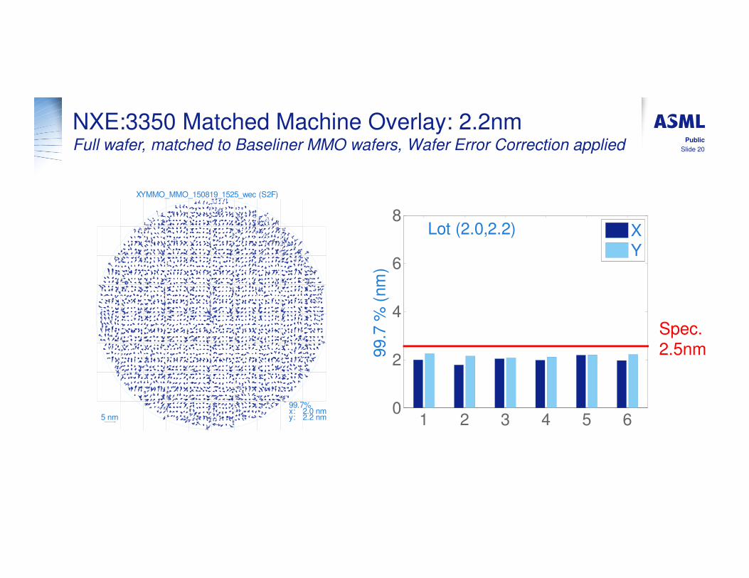
NXE:3350 Matched Machine Overlay: 2.2nm Full wafer, matched to Baseliner MMO wafers, Wafer Error Correction applied
5 nm
99.7%x: 2.0 nmy: 2.2 nm
XYMMO_MMO_150819_1525_wec (S2F)
1 2 3 4 5 60
2
4
6
8Lot (2.0,2.2)
99.7
% (
nm
)
X
Y
Spec.
2.5nm
Slide 21
Public
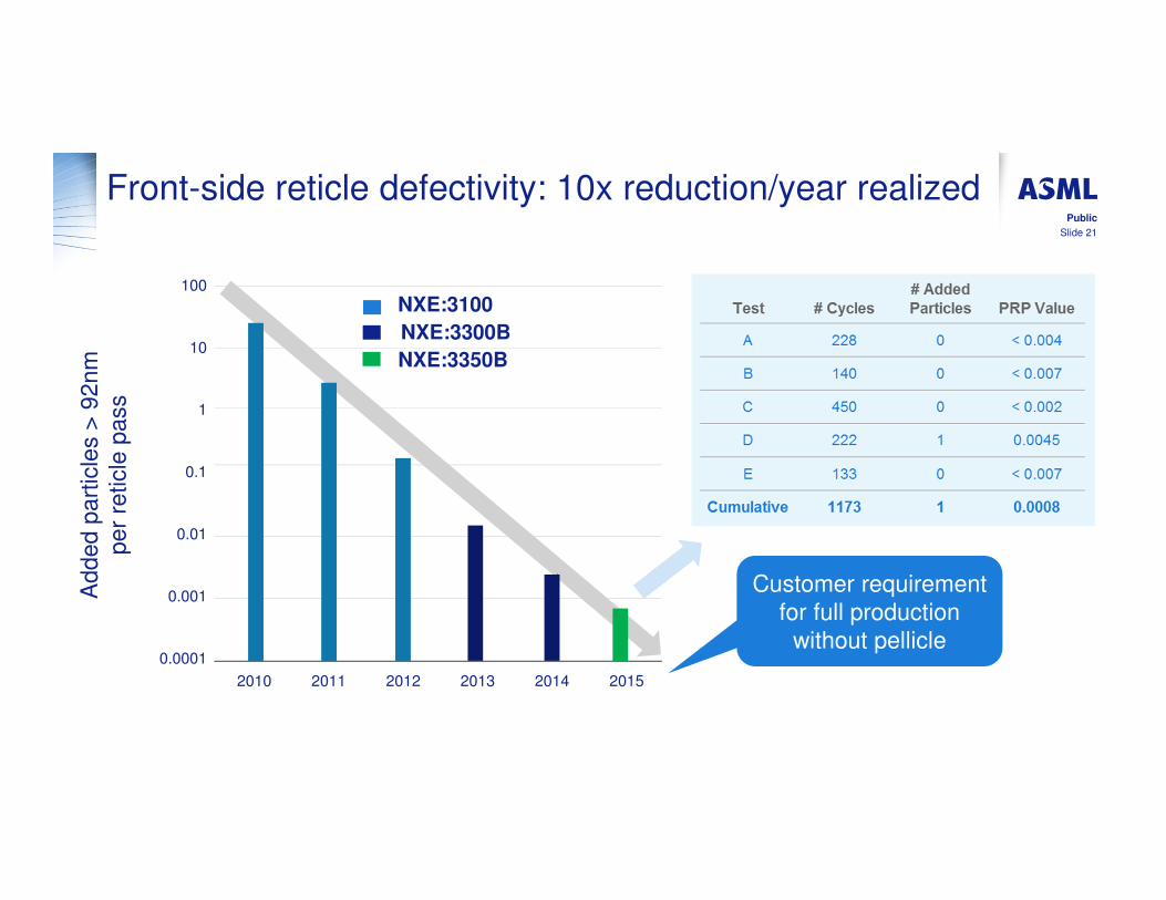
Front-side reticle defectivity: 10x reduction/year realized
Customer requirement
for full production
without pellicle
Ad
de
d p
art
icle
s >
92
nm
pe
r re
ticle
pa
ss
2010 2011 2012 2013 2014 2015
0.0001
0.001
0.01
0.1
1
10
100
NXE:3100
NXE:3300B
NXE:3350B
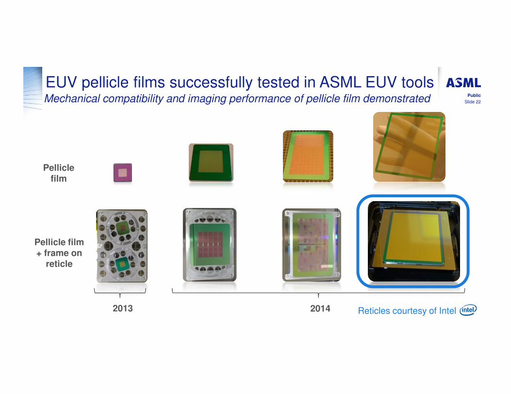
EUV pellicle films successfully tested in ASML EUV tools Mechanical compatibility and imaging performance of pellicle film demonstrated
2013 2014
Pellicle film
Pellicle film + frame on
reticle
Reticles courtesy of Intel
Slide 22
Public
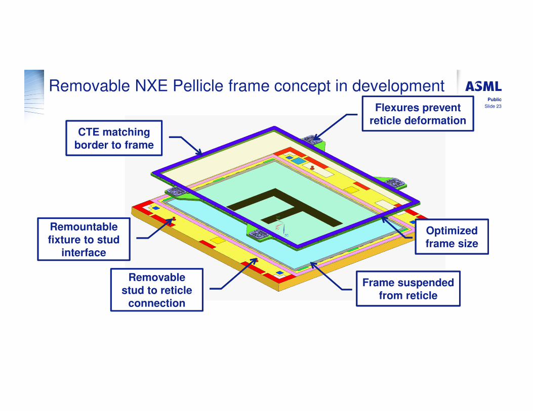
Slide 23
Public
Removable NXE Pellicle frame concept in development
Optimized
frame size
CTE matching
border to frame
Removable
stud to reticle
connection
Remountable
fixture to stud
interface
Frame suspended
from reticle
Flexures prevent
reticle deformation
Public
Slide 24
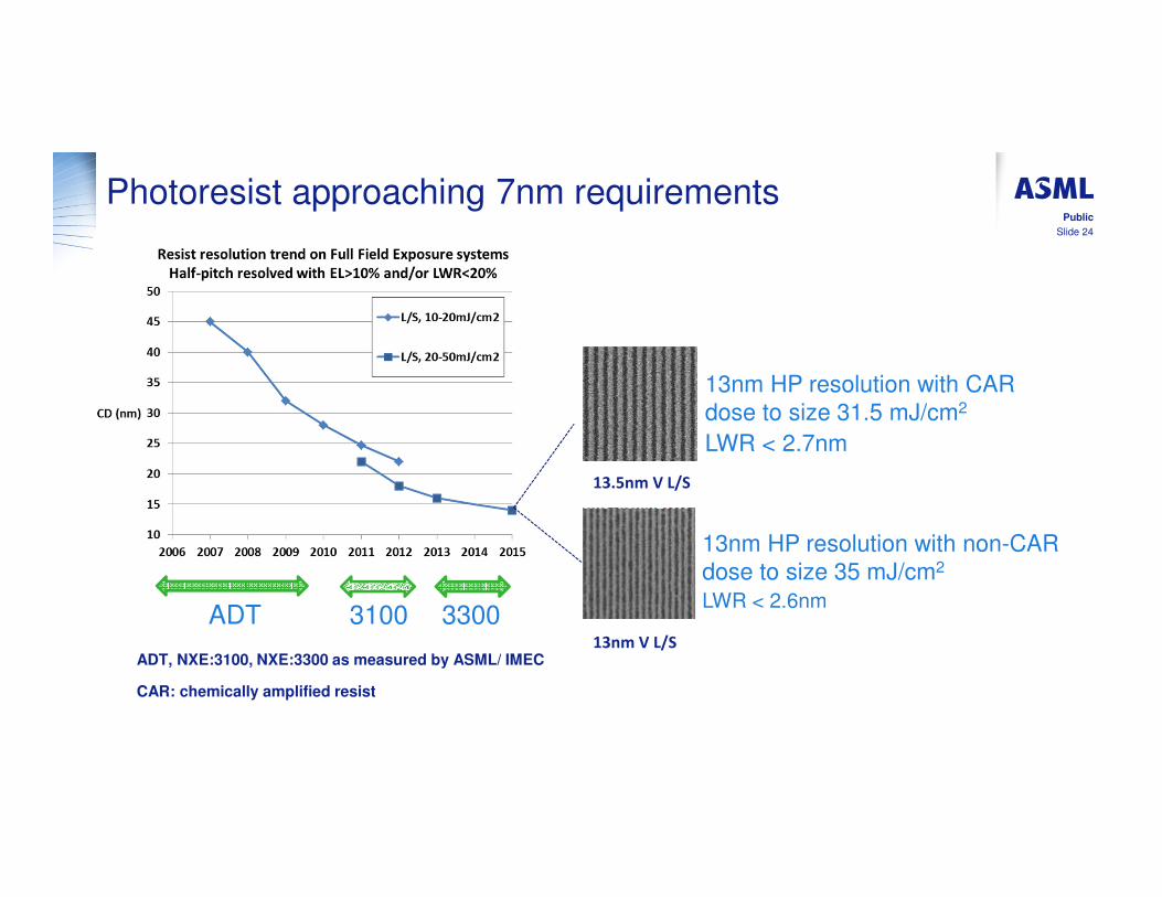
Photoresist approaching 7nm requirements
ADT, NXE:3100, NXE:3300 as measured by ASML/ IMEC
CAR: chemically amplified resist
ADT 3100 3300
13.5nm V L/S
13nm HP resolution with CAR
dose to size 31.5 mJ/cm2
LWR < 2.7nm
13nm V L/S
13nm HP resolution with non-CAR
dose to size 35 mJ/cm2
LWR < 2.6nm
Public
Slide 25
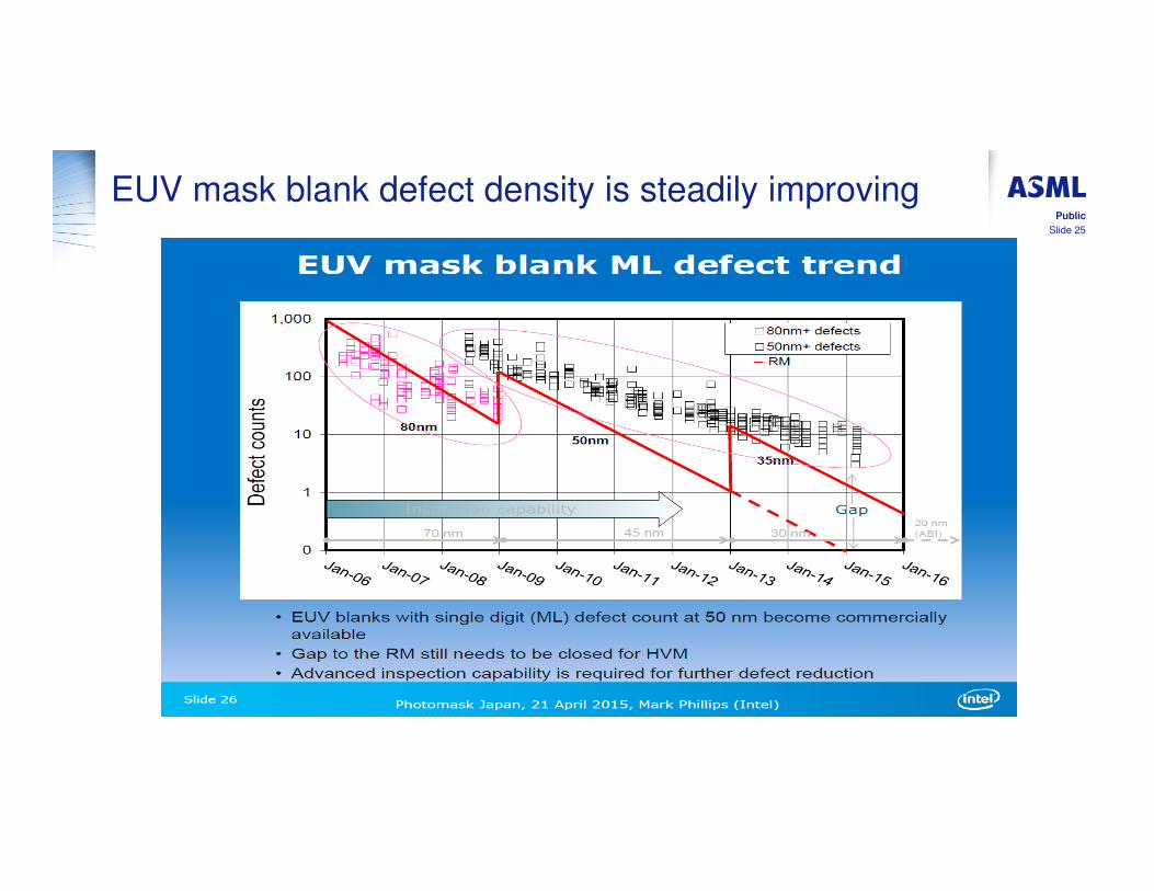
EUV mask blank defect density is steadily improving
EUV Insertion: “WHEN” not “IF”
• Customers differ in exactly “WHEN” EUV will go to volume production
• EUV insertion is focusing on the 7nm node
• Production 2018, production system shipments 2017
• EUV is making continued progress on the Wafers-per-Day roadmap
• >500WpD at multiple customers
• >500WpD over 4 consecutive weeks shown at one customer
• Roadmap in place to deliver 1500 WpD in 2016 for 7nm insertion
• Continued focus on availability to >90%
• EUV imaging & overlay meeting 7nm node requirements
• EUV infrastructure progressing towards 7nm volume production
Public
Slide 26