based on lil - uni-halle.de
TRANSCRIPT

3 TEMPLATED FABRICATION OF NANORING ARRAYS BASED ON LIL 39
3 TEMPLATED FABRICATION OF NANORING ARRAYS
BASED ON LIL
Nanorings, artificial nanoscale clusters, have recently attracted considerable attention
both theoretically and experimentally. Lithographically defined arrays of metallic or
semiconductor nanorings are particularly interesting for applications due to their unique
magnetic, [32~47] optical [48] or electrical properties.
For example, for the application in data storage devices, magnetic memory devices
based on flux-closure magnets were first introduced during the early 1950s. [49] These
non-volatile devices used macroscopic ring-shaped ferrite magnets connected in a grid
using Ni wires, and bits of information are stored by magnetizing each ring structure
clockwise or counterclockwise. The most modern version of magnetic storage is
Magnetic random access memory (MRAM). Recently, beyond elongated or bar-shaped
elements, high density MRAM devices based on ring-shaped magnetoresistive elements
have been proposed. [50] In the last three years, much attention has been drawn towards
elliptical magnetic rings [44~47] with an in-plane magnetic anisotropy. Due to the
existence of more than two stable magnetic states in an elliptical magnetic nanoring
structure, more than one bit to be stored in each element is allowed, for potential
application in novel elliptical-ring-shaped MRAM devices.
Motivated by the application potential, efforts to construct mesoscopic nanorings have
led researchers to explore and develop a variety of fabrication methods. Conventional
lithography techniques such as optical lithography and EBL are limited in spatial
resolution and writing speed, respectively. Alternatively, low-cost template-based
synthesis approaches for ring-shaped nanostructures have been developed very recently.
Nanosphere lithography [51~55] and nanoporous templates [56~59] have been employed for
the fabrication of nanoring arrays.
In case of nanosphere lithography for nanoring arrays, usually self-assembled polymeric
or silica nanospheres or nanoparticles are positioned on planar substrate. Metallic thin

3 TEMPLATED FABRICATION OF NANORING ARRAYS BASED ON LIL 40
films are subsequently deposited onto the nanospheres. Metallic nanorings are obtained
by perpendicular ion-beam bombardment and chemical removal of the nanospheres.
However, the arrangement of the thus obtained nanorings is often random, or ordered
only in small areas when self-ordering strategies are applied for the nanosphere
assembly.
Membrane structures were also utilized for the fabrication of nanoring arrays such as
porous anodic aluminium oxide (AAO) [56~58] and nanochannel glass (NCG). [59] They
are scalable and suitable for the large-area fabrication of arrays of circular-shaped
nanorings. However, the template preparation is cost- and time-consuming. Moreover,
fabrication of elliptical nanoring arrays is not possible with these templates.
As an alternative approach a templated deposition method of perfectly ordered nanoring
arrays based on LIL will be introduced in this chapter. These templates with perfectly
ordered hole array structures were fabricated by LIL exposures and structure transfer
techniques. Electrochemical deposition and atomic layer deposition (ALD) were
employed for the deposition of ring materials. In section 3.1, two novel methods for the
electrodeposition of metallic nanoring or nanowire arrays on patterned highly doped
silicon templates and sacrificial Cr layer electrode are discussed, respectively. The
nanoring arrays generated by ALD and subsequent perpendicular Ar+ sputtering are
introduced in section 3.2.
3.1 ELECTROCHEMICAL DEPOSITION OF NANORING AND
NANOWIRE ARRAYS
3.1.1 TEMPLATED ELECTROCHEMICAL DEPOSITION
Electrochemical deposition combined with resist patterning techniques provides a
powerful tool for the fabrication of micro- and nanostructures. Although in the IC
industry, one tends to avoid wet chemistry, both IC and micromachining needs are
forcing reconsideration of electrochemical deposition as a viable solution. Nowadays,
the electrochemical deposition based LIGA [60] process is a standard technique for the
fabrication of micro devices. The principle of templated electrochemical deposition
3 TEMPLATED FABRICATION OF NANORING ARRAYS BASED ON LIL 41
(ECD) [61~67] is the selective electrodeposition of metals or semiconductors on a
conductive seed layer through openings in an insulating mask. This deposition
technique is characterized by a very high fidelity to the mask.
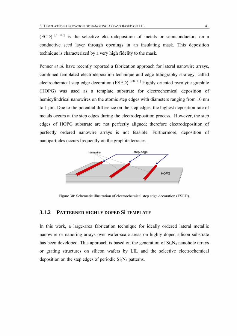
Penner et al. have recently reported a fabrication approach for lateral nanowire arrays,
combined templated electrodeposition technique and edge lithography strategy, called
electrochemical step edge decoration (ESED). [68~71] Highly oriented pyrolytic graphite
(HOPG) was used as a template substrate for electrochemical deposition of
hemicylindrical nanowires on the atomic step edges with diameters ranging from 10 nm
to 1 μm. Due to the potential difference on the step edges, the highest deposition rate of
metals occurs at the step edges during the electrodeposition process. However, the step
edges of HOPG substrate are not perfectly aligned; therefore electrodeposition of
perfectly ordered nanowire arrays is not feasible. Furthermore, deposition of
nanoparticles occurs frequently on the graphite terraces.
Figure 30: Schematic illustration of electrochemical step edge decoration (ESED).
3.1.2 PATTERNED HIGHLY DOPED Si TEMPLATE
In this work, a large-area fabrication technique for ideally ordered lateral metallic
nanowire or nanoring arrays over wafer-scale areas on highly doped silicon substrate
has been developed. This approach is based on the generation of Si3N4 nanohole arrays
or grating structures on silicon wafers by LIL and the selective electrochemical
deposition on the step edges of periodic Si3N4 patterns.

3 TEMPLATED FABRICATION OF NANORING ARRAYS BASED ON LIL 42
Figure 31: Schematic illustration of lithographically guided electrodeposition of ideally ordered metallic
nanowire or nanoring arrays on a highly doped silicon substrate. (a) LIL patterning of PR and
ARC on the substrate; (b) pattern transfer through the underlined Si3N4 and into the highly
doped silicon substrate by RIE with CHF3 gas, removal of the remaining polymer with O2
plasma, and subsequent treatment of the substrate with 5% HF solution; (c) selective
electrodeposition of metal along the step edges; (d) nanoring array deposited on the substrate
with hole patterns; (e) nanowire array deposited on line patterns.
Figure 31 (a-c) schematically illustrated the fabrication procedure. PR and ARC on
highly doped silicon (resistivity ca. 0.01-0.02 Ω-cm) wafer covered with a 35 nm thick
Si3N4 layer were first patterned by LIL into periodic lines or holes patterns. The
polymer (PR and ARC) structures generated by LIL served as etching masks for an
anisotropic RIE through the Si3N4 layer and they were also overetched into the Si
substrate. After the pattern transfer process the remaining polymer resists were removed
by O2 plasma, which also leads to the formation of silicon oxide in the opened parts.
Prior to the electrodeposition process, the sample was treated with 5% HF solution for
90 sec to remove partly the thin oxide layer at the step edges caused by native oxidation
or O2 plasma treatment. Subsequently, the silicon substrate with the Si3N4 pattern was
utilized as the working cathode for the electrochemical deposition of metals. The
insulating layer of Si3N4 on the mesas and the native oxide layer in the valleys ensured

3 TEMPLATED FABRICATION OF NANORING ARRAYS BASED ON LIL 43
that the electrochemical deposition of metal occurred exclusively on the etched
undercuts of the patterns and not everywhere on the top surface of the template. The
current density was adjusted according to the area and structure density of the
templates. In the present method, on samples with hole (Figure 31d) and line patterns
(Figure 31e), arrays of nanorings and nanowires were obtained, respectively.
With this novel approach, the thickness of the nanoring/nanowire in cross-section could
be controlled by monitoring the amount of total integrated charges involved in the
electrochemical reaction, i.e. the current density and the deposition time. The shape and
the arrangement of the nanorings/nanowires could be controlled by the LIL patterning
process. Typically, feature sizes ranging from 50 to 300 nm and nanorings with
different aspect ratios in shape can be obtained by our approach.
Figure 32: SEM images of Au nanowire array with a wire diameter of 110 nm in (a) top-view and (b)
cross-section view.
Fabrication of nanowire arrays by using substrates with lines patterns has also been
demonstrated (Figure 32). Arrays of ideally ordered metal nanowires on Si substrates of
several centimeters were realized in our experiments. In comparison with the ESED
method, in our approach the arrangement of the nanowires can be varied over a broad
range and the length of the nanowires can be extended over a whole wafer. In addition,
it is worth noting that in each groove, two parallel nanowires were deposited on both
edges. This enables us to achieve nanowire arrays with half of the periodicity of LIL-
defined pattern.

3 TEMPLATED FABRICATION OF NANORING ARRAYS BASED ON LIL 44
Figure 33: Representative SEM images of arrays of Au nanorings with different geometries. (a) Circular
ring array; (b) hexagonally arranged elliptical ring array in top view and (d) in cross-section
view; (c) elliptical ring array.
Figure 33 shows representative SEM images of Au nanoring arrays with different
feature sizes and aspect ratios in top- and cross-section views. Figure 33a shows an
array of circular-shaped rings, which have a wire thickness of 103 nm, a ring inner
diameter of 1070 nm and a 1300 nm periodicity. Figure 33b and d are top- and oblique-
views showing a hexagonal array of elliptical rings with a wire diameter of 57 nm, a
long-axis diameter of 1250 nm, a short-axis diameter of 680 nm and a center-to-center
spacing of 1330 nm. Figure 33c demonstrates elliptical rings with high aspect ratio
(11:1 in long-axis:short-axis) and a wire diameter of 189 nm.
In order to investigate the mechanisms of the selective deposition on the undercuts of
the structures, TEM specimens of the topographic profile of the sample shown in Figure
33b has been prepared and images have been taken with a Phillips CM 20 STEM. The
cross-section of the silicon substrate, the step edges and the gold nanowires can be seen
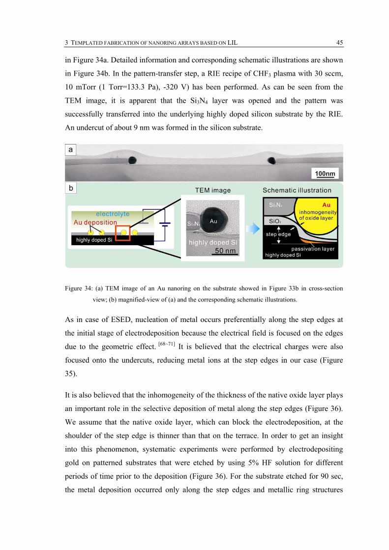
3 TEMPLATED FABRICATION OF NANORING ARRAYS BASED ON LIL 45
in Figure 34a. Detailed information and corresponding schematic illustrations are shown
in Figure 34b. In the pattern-transfer step, a RIE recipe of CHF3 plasma with 30 sccm,
10 mTorr (1 Torr=133.3 Pa), -320 V) has been performed. As can be seen from the
TEM image, it is apparent that the Si3N4 layer was opened and the pattern was
successfully transferred into the underlying highly doped silicon substrate by the RIE.
An undercut of about 9 nm was formed in the silicon substrate.
Figure 34: (a) TEM image of an Au nanoring on the substrate showed in Figure 33b in cross-section
view; (b) magnified-view of (a) and the corresponding schematic illustrations.
As in case of ESED, nucleation of metal occurs preferentially along the step edges at
the initial stage of electrodeposition because the electrical field is focused on the edges
due to the geometric effect. [68~71] It is believed that the electrical charges were also
focused onto the undercuts, reducing metal ions at the step edges in our case (Figure
35).
It is also believed that the inhomogeneity of the thickness of the native oxide layer plays
an important role in the selective deposition of metal along the step edges (Figure 36).
We assume that the native oxide layer, which can block the electrodeposition, at the
shoulder of the step edge is thinner than that on the terrace. In order to get an insight
into this phenomenon, systematic experiments were performed by electrodepositing
gold on patterned substrates that were etched by using 5% HF solution for different
periods of time prior to the deposition (Figure 36). For the substrate etched for 90 sec,
the metal deposition occurred only along the step edges and metallic ring structures

3 TEMPLATED FABRICATION OF NANORING ARRAYS BASED ON LIL 46
were successfully formed. Whereas electrodeposition on the substrate etched for 120
sec results in a high density of metallic dots on the Si valley surfaces.
Figure 35: Schematic illustration of focusing of the electric field on the overetched undercut due to
geometric effect during the electrodeposition.
Figure 36: SEM micrographs and the corresponding schematic illustrations of the effect of HF treatment
on the deposition results. (a) Successfully selective metal deposition; (b) granular gold films
on the patterned Si substrates. Before electroplating, the samples were treated with 5% HF
solution for (a) 90 sec and (b) 120 sec.
The SiO2 layer along the step edges is preferentially removed by a short HF etching

3 TEMPLATED FABRICATION OF NANORING ARRAYS BASED ON LIL 47
(<90 sec), whereas the Si valley surfaces were still covered with an oxide layer, i.e.,
only the step edges were exposed to the electrolyte and the deposition took place there
(Figure 36a). After 120 sec HF etching, the oxide layer on the valley surface was also
completely removed. As a result, a selective electroplating can not be achieved, and
metal deposition could take place on the entire surface uncovered with the Si3N4 mask
(Figure 36b). As can be seen from the insert of Figure 36b, the density of metal
deposition along the step edge is clearly higher than in the Si valley. We can deduce that
the topography of the step edges leads to a preferential nucleation during the
electrodeposition process, although the oxide layer has been completely removed. The
geometric effect produced an energetic disparity for the electrodepostion.
If we summarize the mechanism of the selective electroplating in this work (recall
Figure 34b), five major arguments could be considered to positively affect the forming
of nanoring and nanowire arrays:
The resist pattern was transferred into the conductive silicon substrate for
5~10 nm by RIE. The topographic profile induced a preferential nucleation
at the step edges;
During the removal of the polymer by RIE with O2 plasma, an amorphous
passivation layer could be generated in the valleys of the Si substrate,
which has the potential to prevent the valley surfaces from direct
electrodeposition;
The inhomogeneity of the oxide layer enables the preferential exposure of
the step edges to the electrolyte, which leads to a selective electroplating;
The strong focusing effect of the electric field at the shoulders of the step
edges during the electrodeposition results in selective reduction of metal
ions there;
The electric-field-assisted fast diffusion of metal ions towards the step
edges guides strongly the selective deposition.

3 TEMPLATED FABRICATION OF NANORING ARRAYS BASED ON LIL 48
3.1.3 DEPOSITION OF NANORINGS ON METALLIC ELECTRODES
The major difficulty of the method introduced above is that the etching of the native
SiO2 layer on a highly doped silicon substrate prior to the electrodeposition is difficult
to be precisely controlled. Therefore, a second generation of templates with a metallic
electrode contact has been developed. Figure 37 schematically illustrates the process of
this method in cross-section view. A Cr layer with a thickness of 20 nm was sputtered
on a silicon wafer with a 100 nm oxide layer prior to the resist deposition. Desired
periodic holes or grating structures were obtained by LIL exposures and subsequently
transferred through the Cr layer by RIE with Cl2 gas. The patterned Cr layer was used as
working electrode for the electrodeposition. The Cr layer was recessed in a resist and
SiO2 sandwich, which ensures that the metal deposition occurred only along the
exposed edges of Cr layer.
Figure 37: Schematic illustration of electrodeposition of nanoring arrays on sacrificial Cr layer electrode.
(a) LIL patterning of the PR and ARC deposited on the substrate; (b) pattern transfer through
the buried Cr layer; (c) electrodeposition of metal along the edges of Cr pattern.

3 TEMPLATED FABRICATION OF NANORING ARRAYS BASED ON LIL 49
Parallel to our work, Penner and his co-workers published a similar method, called
lithographically patterned nanowire electrodeposition (LPNE). [72] Nickel was chosen in
that case as sacrificial layer for the preparation of a nanoband electrode and the exposed
nickel layer was removed locally electrochemically. In our approach, Cr layer has been
employed because it is a lithographically compatible material, such as for RIE process,
and it will not affect the measurements of magnetic properties of the as-prepared
nanoring structures. In comparison to nickel, Cr is much easier to be oxidized, which
could block the electrodeposition. Therefore, a HF etching prior to the electrodeposition
was performed to remove the native CrO2 layer on the exposed working electrode.
8 μm8 μm8 μm
900 nm
10 µm
900 nm
Figure 38: SEM iamge of as-prepared elliptical Ni nanoring array, magnified view is shown as insert.
Figure 38 shows the SEM image of an as-prepared elliptical Ni nanoring array with
magnified view as insert. The elliptical rings are hexagonally arranged and have a
diameter in the long-axis of 1230 nm and in the short-axis of 400 nm, which gives an
aspect ratio of ca. 3.1 (long-axis: short-axis). The center to center distance is about 740
nm and the diameter of the deposited ring-like metal wires is below 60 nm. It is
apparent from the SEM image that this approach provides a homogenous deposition of
metals along the step edges of resist structures and therefore allows the generation of
complex structures, e.g. nanowire arrays. After the deposition of desired materials along
the step edges, the photoresist and the sacrificial Cr layer could be selective etched

3 TEMPLATED FABRICATION OF NANORING ARRAYS BASED ON LIL 50
away by RIE and chemically, respectively. Thus freestanding nanoring or nanowire
arrays could be obtained on normal silicon substrates, which will not influence the
characterization of the properties of the structures, such as magnetic, electric, optic and
thermoelectric properties, etc. Room temperature hysteresis loop measurements of the
nanoring arrays shown in Figure 38 were obtained using a SQUID (Superconducting
Quantum Interference Device)-Magnetometer. Figure 39 shows the hysteresis loops on
applying a magnetic field parallel and perpendicular to the long axis of the elliptical
rings, respectively. The long-axis was determined by optical microscopy. On applying a
magnetic field parallel to the long-axis, the collective magnetization reversal of the
array shows an easy-axis behavior, while applying a field perpendicular to the long-axis
displays a hard-axis behavior. The results indicate that the elliptical shape anisotropy
dominates the magnetization reversal of this array at room temperature.
-2000 -1000 0 1000 2000
-1,0
-0,5
0,0
0,5
1,0
M/M
1T
H [Oe]
short axis long axis
HH
Ni ellipseaspect ratio = 3.1
-2000 -1000 0 1000 2000
-1,0
-0,5
0,0
0,5
1,0
M/M
1T
H [Oe]
short axis long axis
HH
HH
Ni ellipseaspect ratio = 3.1
Figure 39: Room temperature hysteresis loop measurements on applying magnetic fields parallel and
perpendicular to the long axis of Ni elliptical ring array, respectively.
Ni0.8Fe0.2 permalloy nanoring array was also prepared with the same template. Room

3 TEMPLATED FABRICATION OF NANORING ARRAYS BASED ON LIL 51
temperature hysteresis loops on applying a magnetic field parallel and perpendicular to
the long axis of the ellipses have also been measured with a SQUID-Magnetometer.
Figure 40 shows the results of measurements of magnetic properties. Both loops display
that switching in this ring structures is a complex multistep process rather than a two
step process shown in the Ni ring array above. The slanted plateau between transitions
and the slope of the transitions suggest that the rings exhibit the vortex and onion state. [46]
-2000 -1000 0 1000 2000
-1.0
-0.5
0.0
0.5
1.0
M/M
0.2T
H [Oe]
Ni0.8Fe0.2 long axis @ RT Ni0.8Fe0.2 short axis @ RT
HH
Ni0.8Fe0.2aspect ratio = 3.1
-2000 -1000 0 1000 2000
-1.0
-0.5
0.0
0.5
1.0
M/M
0.2T
H [Oe]
Ni0.8Fe0.2 long axis @ RT Ni0.8Fe0.2 short axis @ RT
HH
HH
Ni0.8Fe0.2aspect ratio = 3.1
Figure 40: Room temperature hysteresis loop measurements on applying magnetic fields parallel and
perpendicular to the long axis of Ni0.8Fe0.2 permalloy elliptical ring array, respectively.
Adeyeye et al. have reported the spin state evolution and in-plane magnetic anisotropy
of elongated Ni0.8Fe0.2 nanorings in 2005. [47] They have fabricated permalloy elongated
nanorings by using deep UV lithography on a 4x4 mm2 area and lift-off processes. The
room temperature magnetization curve (Figure 41a) of the rings was measured using
vibrating sample magnetometer (VSM) and the hysteresis loop of a single ring was
simulated (Figure 41b). Both experimental and theoretical results display a number of

3 TEMPLATED FABRICATION OF NANORING ARRAYS BASED ON LIL 52
transitions in the magnetization states as the applied field is varied from saturation field
Hs in one direction to Hs in the other. Compared to their results, our magnetic hysteresis
loops (Figure 40) of permalloy elliptical nanoring arrays show similar complexities and
magnetic anisotropy. However, our fabrication method provides a better resolution and
flexibility.
Figure 41: Results from the Ref [47]: (a) Magnetic hysteresis loop of arrays of elongated 30-nm-thick
Ni0.8Fe0.2 rings when the applied field is along the major axis; (b) simulated hysteresis loop of a
single elongated 30-nm-thick Ni0.8Fe0.2 ring.
3 TEMPLATED FABRICATION OF NANORING ARRAYS BASED ON LIL 53
3.2 ATOMIC LAYER DEPOSITION (ALD) OF NANORING
ARRAYS
3.2.1 PRINCIPLE OF ALD
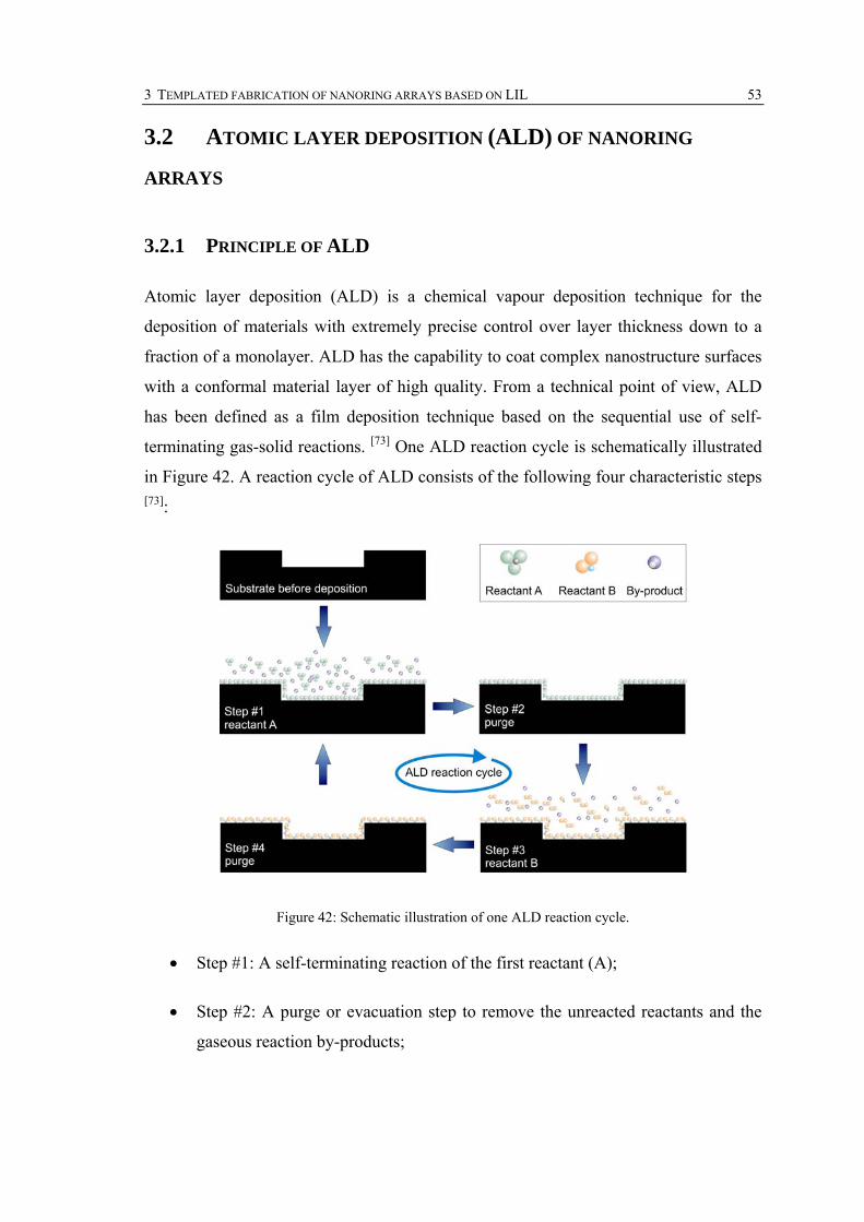
Atomic layer deposition (ALD) is a chemical vapour deposition technique for the
deposition of materials with extremely precise control over layer thickness down to a
fraction of a monolayer. ALD has the capability to coat complex nanostructure surfaces
with a conformal material layer of high quality. From a technical point of view, ALD
has been defined as a film deposition technique based on the sequential use of self-
terminating gas-solid reactions. [73] One ALD reaction cycle is schematically illustrated
in Figure 42. A reaction cycle of ALD consists of the following four characteristic steps
[73]:
Figure 42: Schematic illustration of one ALD reaction cycle.
• Step #1: A self-terminating reaction of the first reactant (A);
• Step #2: A purge or evacuation step to remove the unreacted reactants and the
gaseous reaction by-products;

3 TEMPLATED FABRICATION OF NANORING ARRAYS BASED ON LIL 54
• Step #3: A self-terminating reaction of the second reactant (B) or another
treatment to achieve the surface again for the reaction of reactant A;
• Step #4: A purge or evacuation step.
A certain amount of material is deposited on the surface by each reaction cycle. To
grow a material layer, reaction cycles are repeated until the desired thickness of material
has been deposited. Because of the surface control, extremely conformal and uniform
material coatings are obtained. In this work, TiO2 and Al2O3 deposition have been
performed for nanoring (this section) and nanochannel (section 5.3) arrays.
3.2.2 ALD OF NANORING ARRAYS
The fabrication method of nanoring arrays by template based ALD deposition and Ar+
sputtering is schematically illustrated in Figure 43. The polymer hole array generated by
LIL were transferred into the underlying 25 nm thick SiO2 layer and used as template
for the ALD of TiO2 layer at room temperature (RT). The entire topography of the
template was coated with a homogenous TiO2 layer. Subsequently, a perpendicular Ar+
bombardment was performed to remove the top- and bottom-parts of the TiO2 coating
and therefore independent TiO2 nanoring structures were obtained in the polymer holes.
Finally the polymers were removed by RIE with O2 plasma in order to achieve a free-
standing TiO2 nanoring array.
Figure 44 shows the representative SEM micrographs. A template coated with a
uniform TiO2 layer obtained by ALD at RT is presented in Figure 44a. After a
perpendicular Ar+ bombardment, a perfectly square-like arranged circular TiO2
nanoring array has been achieved. The rings have an inner diameter of 119 nm, a wall
thickness of the ring of ~34 nm, and a center-to-center spacing of 370 nm.

3 TEMPLATED FABRICATION OF NANORING ARRAYS BASED ON LIL 55
Figure 43: Schematic illustration of fabrication of nanoring arrays by template based ALD of TiO2 and Ar
sputtering. (a) Template with hole array structures was fabricated by means of LIL, and the
structures were transferred into the underlying SiO2 layer by RIE with CHF3 gas; (b) ALD of
TiO2 layer on the substrate surface at RT; (c) perpendicular Ar+ sputtering to remove the top-
and bottom-parts of the TiO2 layer; (d) release the separated TiO2 nanoring arrays from the
polymer structures by O2 plasma RIE.
Figure 44: SEM images of (a) cross-section view of a template coated with a uniform TiO2 layer and (b)
top-view of square arranged TiO2 nanoring array. A magnified view is shown as an insert, the
wall thickness of the ring is ~34 nm.
With this method, the diameter, ring-shape and arrangement could be adjusted by the
LIL process, which provides a flexible variation of such parameters. The thickness of
the wall of the rings could be precisely controlled by varying the number of ALD
cycles. However, the Ar+ bombardment is not suitable for the removal of a very thick
layer (>35 nm), otherwise the homogeneity of the surface could not be guaranteed. For
a thick ring wall or a multilayered nanoring array, repeating of the process steps from
(a) to (c) in Figure 43 is proposed. Due to the conveniences of ALD, a broad range of

3 TEMPLATED FABRICATION OF NANORING ARRAYS BASED ON LIL 56
materials can be used easily in this method. Even magnetic materials for magnetic ring
arrays, which are interesting for applications, could be deposited directly or obtained by
reducing oxides such as NiO or Fe2O3 into Ni or Fe3O4, respectively, in a hydrogen
atmosphere. In addition, ring arrays with extremely small thickness, e.g. even several
nanometer are feasible.
3.3 SUMMARY
In this chapter, LIL has been employed for the definition of locations and shapes of
nanoring arrays. By double exposures, perfectly ordered circular or elliptical structure
arrays have been fabricated in photoresist layers on a desired substrate and used as
templates. Large-area ordered metallic nanoring arrays have been obtained by
electroplating of metals along the step edges of resist structures on the templates. A
second generation of substrate has been developed with metallic electrodes. Uniform
metal deposition along the step edges of resist structures and, therefore, homogenous
nanoring arrays have been obtained. Combination of room temperature ALD of TiO2 on
the template and subsequent Ar+ bombardment provides another novel approach for the
parallel synthesis of nanoring arrays of various functional materials.