2018 vortrag ptb braunschweig - uni-halle.de
TRANSCRIPT

R. Krause-RehbergUniversität Halle, Inst. für Physik
• Some historical remarks• Techniques of Positron Annihilation• Study of Defects in Semiconductors• User-dedicated Positron Facilities in Germany (FRM-II & ELBE)
Material Science using Positron Annihilation
9.3.2018
19:49

Discovery of the Positron
• Positron was predicted in 1928 by Paul A.M. Dirac
• Discovery in 1932 in cloud chamber pictures by C.D. Anderson
first Identification of a positron in a cloud chamber 5 mm lead plate photo taken by C.D. Anderson
P.A.M. Dirac
C.D. Anderson
• Positronium as bound state of e- and e+
lightest atom was predicted (1934) and discovered (1951)
• Annihilation in matter was studied beginning in the 40s
• Positrons can be obtained by
- pair production from gamma radiation (E > 1022 keV)
- β+ decay from isotopes (mostly 22Na)
Martin-Luther-Universität Halle 19:49

Electron structure of solids can be discovered
• during annihilation: conservation laws must be fulfilled (energy, momentum)
• positron cools down to thermal energies ->
• energy of annihilating electron-positron pair ≈ energy of electron
• electron momentum distribution can directly be measured
Martin-Luther-Universität Halle 19:49

Martin-Luther-Universität Halle
• now: two-dimensional (position-sensitive) detectors
• measurement of single crystals in different directions:
• reconstruction of Fermi surface possible
2D – ACAR (Angular Correlation of Annihilation Radiation)
19:49

2D-ACAR of Copper
(Berko, 1979)
py along [010]
p zal
ong
[100
]Theory Experiment
Fermi surface of copper
Martin-Luther-Universität Halle 19:49

• 1950…1960: in addition to ACAR -> different experimental techniques were developed
• Positron lifetime spectroscopy and Doppler broadening spectroscopy
• end of 60s: lifetime is sensitive to lattice imperfections- Brandt et al. (1968): vacancies in ionic crystals- Dekhtyar et al. (1969): plastically deformed semiconductors- McKenzie et al. (1967): vacancies in thermal equilibrium in
metals
• Positrons are localized (trapped) by open-volume defects
Positrons are sensitive for Crystal Lattice Defects
Martin-Luther-Universität Halle 19:49

Vacancies in thermal Equilibrium
• Vacancy concentration in thermal equilibrium:
• in metals HF ≈ 0.5 ... 4 eV ⇒at Tm [1v] ≈ 10-4...-3 /atom
• fits well to the sensitivity range of positron annihilation
Tungsten
W p
aram
eter
Temperature (K)(Ziegler, 1979)
fit to trapping model
Martin-Luther-Universität HalleMartin-Luther-Universität Halle 19:49

The positron lifetime spectroscopy
• positron wave-function can be localized in the attractive potential of a defect
• annihilation parameters change in the localized state
• e.g. positron lifetime increases in a vacancy EB+≈ 1eV
• lifetime is measured as time difference between appearance of 1.27 (start) and 0.51 MeV (stop) quanta
• defect identification and quantification possible
22Na
19:49Martin-Luther-Universität Halle
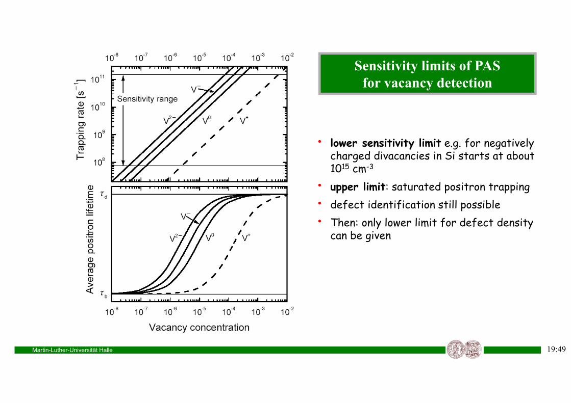
Sensitivity limits of PAS for vacancy detection
• upper limit: saturated positron trapping• defect identification still possible• Then: only lower limit for defect density
can be given
• lower sensitivity limit e.g. for negatively charged divacancies in Si starts at about 1015 cm-3
19:49Martin-Luther-Universität Halle

• in a metal: charge of a vacancy is effectively screened by free electrons• they are not available in semiconductors• thus, long-range Coulomb potential added• positrons may be attracted or repelled • trapping coefficient is function of charge state
Vacancies in a semiconductor may be charged
19:49Martin-Luther-Universität Halle

Digital positron lifetime measurement
Martin-Luther-Universität Halle 19:49Martin-Luther-Universität Halle

Screenshot of two digitized anode pulses
time difference = 2.65471 samples = 663.67 ps
19:49

Martin-Luther-Universität Halle 19:49Martin-Luther-Universität Halle

0 1 2 3 4 5
103
104
105
106
b = 218 ps
3 = 520 ps
2 = 320 ps
As–grown Cz Si Plastically deformed Si
Cou
nts
Time [ns]
Positron lifetime spectroscopy
Martin-Luther-Universität Halle
• positron lifetime spectra consist of exponential decay components
• positron trapping in open-volume defects leads to long-lived components
• longer lifetime due to lower electron density
• analysis by non-linear fitting: lifetimes iand intensities Ii
trapping rate defect concentration
trapping coefficient
positron lifetime spectrum:
(divacancies)
(vacancy clusters)(bulk)
19:49Martin-Luther-Universität Halle

Doppler Broadening Spectroscopy
19:49Martin-Luther-Universität Halle

Measurement of Doppler Broadening
electron momentum in propagation direction of 511 keV -ray leads to Doppler broadening of annihilation line
can be detected by conventional energy-dispersive Ge detectors and standard electronics
19:49Martin-Luther-Universität Halle

Line Shape Parameters
S parameter:
S = AS/A0
W parameter:
W = AW/A0
W parameter mainly determined by annihilations of core electrons (chemical information)
19:49Martin-Luther-Universität Halle

Doppler Coincidence Spectroscopy
coincident detection of second annihilation reduces background
use of a second Ge detector improves energy resolution of system
19:49Martin-Luther-Universität Halle

Doppler Coincidence Spectra
E1+E2= 2 m0 c2 =1022 keV19:49Martin-Luther-Universität Halle

• Chemical sensitivity due to electrons at high momentum (core electrons)• a single impurity atom aside a vacancy is detectable• examples: VGa-TeAs in GaAs:Te
Doppler-Coincidence-Spectroscopy in GaAs
J. Gebauer et al., Phys. Rev. B 60 (1999) 1464
19:49Martin-Luther-Universität Halle

Moderation of Positrons
• broad + positron emission spectrum
• deep implantation into solids
• not useful for study of defects in thin layers
• for defect depth profiling: moderation necessary
• monoenergetic positrons can be implanted to different depth
Mean implantation depth of un-moderated positrons from a 22-Na source (1/e) in Si: 50µm
19:49Martin-Luther-Universität Halle
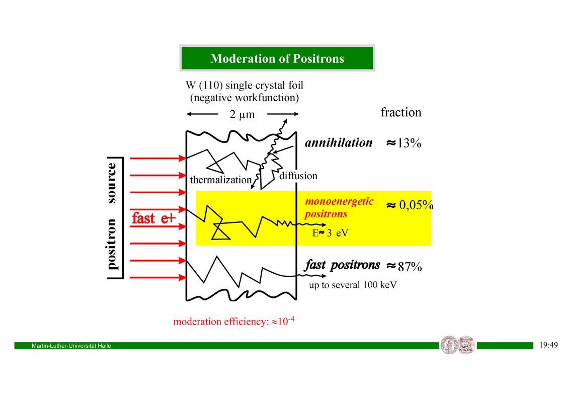
Moderation of Positrons
moderation efficiency: 10-4
19:49Martin-Luther-Universität Halle

The Positron Beam System at Halle University
• spot diameter: 4 mm• time per single Doppler measurement: 20 min• time per depth scan: 8 hours• no lifetime measurements
19:49Martin-Luther-Universität Halle

19:49

Defects in Si induced by Ion Implantation
• ion implantation is most important doping technique in planar technology• main problem: generation of defects ⇒ positron beam measurements
(Eichler et al., 1997)
19:49Martin-Luther-Universität Halle

Point defects determine properties of materials
• Point defects determine electronic and optical properties
• Point defects are generated by crystal growth, irradiation, by plastic deformation, by diffusion, …
• Metals in high radiation environment -> formation of voids -> embrittlement
without vacancies with 0.001% vacanciestransparent opaque
1 vacancy in 100000 atoms
Galliumphosphide1 cm
19:49Martin-Luther-Universität Halle

Defects in electron-irradiated Ge
(Polity et al., 1997)
Ge
e- irr. at 4K
• Electron irradiation (2 MeV @ 4K) induces Frenkel pairs (vacancy - interstitial pairs)• steep annealing stage at 200 K• at high irradiation dose: divacancies are formed (thermally more stable)
19:49Martin-Luther-Universität Halle
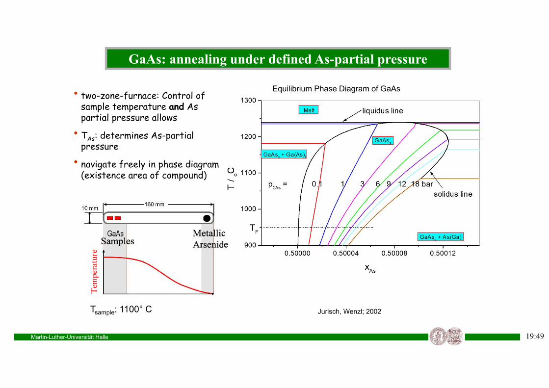
• two-zone-furnace: Control of sample temperature and As partial pressure allows
• TAs: determines As-partial pressure
• navigate freely in phase diagram (existence area of compound)
Tsample: 1100° C
GaAs: annealing under defined As-partial pressure
Jurisch, Wenzl; 2002
Equilibrium Phase Diagram of GaAs
19:49Martin-Luther-Universität Halle

0,01 0,1 1 10
1017
GaAs:Si
Linear fit
Vaca
ncy
conc
entra
tion
(cm
-3)
Arsenic pressure (bar) 0,1 1 10
1016
1017
1018
[Te] in cm-3
9x10¹⁶
4x10¹⁷
6x10¹⁸
2x10¹⁸
231
GaAs:Te
250
235
240
245
av a
t 55
0 K
(ps)
Vaca
ncy
conc
entra
tion
(cm
-3)
Arsenic pressure (bar)
SiGa-VGa TeAs-VGa
Fit: [VGa-Dopant] ~ pAsn
n = 1/4
Thermodynamic reaction:1/4 As4
gas AsAs + VGa
Mass action law:[VGa] = KVG pAs
1/4
J. Gebauer et al.,Physica B 273-274, 705 (1999)
GaAs: Annealing under defined As pressure
19:49Martin-Luther-Universität Halle

Thermodynamic reaction:AsAs VAs + 1/4As4
gas
Mass action law:[VAs] = KVAs pAs
-1/4
Fit: [V-complex] ~ pAsn
n = -1/4
undoped GaAs: As vacancy
Comparison of doped and undoped GaAs
Bondarenko et al., 2003
19:49Martin-Luther-Universität Halle

EL2 in GaAs: important Antisite Defect
• interesting feature: EL2 exhibits metastability• illumination at low temperature properties changes (e.g. no IR absorption
any more)• many structural models were discussed• Dabrowski/Scheffler and Chadi/Chang: EL2 is isolated AsGa and in metastable
state the antisite atom moves outward and leaves a VGa• Metastability is lost during warming-up to 115 K
19:49Martin-Luther-Universität Halle

EL2 in GaAs: important antisite Defect
• before annihilation, diffusing positrons can be trapped by such defects
• as a consequence: positron lifetime increases due to the reduced electron density in the vacancy
• experiment shows the existence of a Gavacancy in the metastable state of GaAs, which does not exist in stable ground state
• was prove of AsGa model of EL2
R. Krause et al.: Observation of a monovacancy in the metastable state of the EL2 defect in GaAs by positron annihilationPhys. Rev. Lett. 65 (26), 3329-32 (1990).
19:49Martin-Luther-Universität Halle

1 2 3 4 5 6 7 8 90.0
0.1
0.2
1 2 3 4 5 6 7 8 9lattice spacing in [110] direction
Hei
ght [
nm]
-2.0 V +1.4 Voccupied empty states
• Scanning tunneling microscopy at GaAs (110)- cleavages planes (by Ph. Ebert, Jülich)
• Defect complex identified as VGa-SiGa
1018 1019
1017
1018
1019
Si concentration (cm-3)
Positrons - cvac STM - [SiGa-VGa]
Def
ect c
once
ntra
tion
(cm
-3)
• Quantification Agreement
Mono-vacancies in GaAs:Si are VGa- SiGa-complexes
Identification of VGa-SiGa-Complexes in GaAs:Si
Gebauer et al., Phys. Rev. Lett. 78 (1997) 333419:49

• there are cluster configurations with a large energy gain
• „Magic Numbers“ with 6, 10 und 14 vacancies
• positron lifetime increases distinctly with cluster size
• for n > 10 saturation effect, i.e. size cannot be determined
Theoretical calculation of vacancy clusters in Si
T.E.M. Staab et al., Physica B 273-274 (1999) 501-504
19:49Martin-Luther-Universität Halle

Experiments on as-grown Silicon
19:49Martin-Luther-Universität Halle
[SiVac] 4×1015 cm-3

Experiments in 2017 on 28Silicon
19:49Martin-Luther-Universität Halle

Running DFG project: Al-Cu alloys
19:49Martin-Luther-Universität Halle
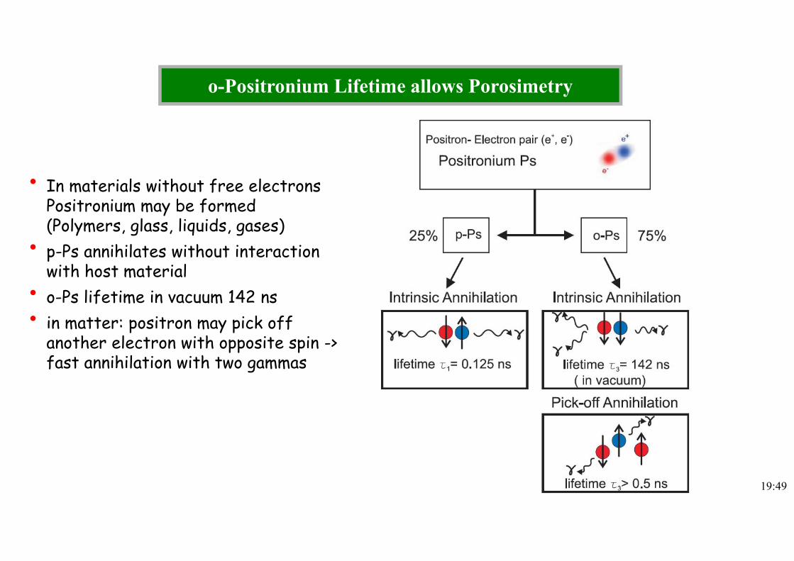
o-Positronium Lifetime allows Porosimetry
• In materials without free electrons Positronium may be formed (Polymers, glass, liquids, gases)
• p-Ps annihilates without interaction with host material
• o-Ps lifetime in vacuum 142 ns• in matter: positron may pick off
another electron with opposite spin -> fast annihilation with two gammas
19:49

Pick-off Annihilation
pick-off annihilation:• o-Ps is converted to p-Ps by capturing an
electron with anti-parallel spin• happens during collisions at walls of pore• lifetime decreases rapidly• lifetime is function of pore size 1.5 ns to 142 ns
positrons form Ps
= 1…142 ns
= 125 ps
19:49Martin-Luther-Universität Halle

o-Ps lifetime 4 versus pore size in CPG Glass
● we measured porous CPG glass in a broad pore size range
● given pore size obtained by N2-adsorption and/or mercury intrusion technique
● for T=300 K fair agreement to the RTE model
S.Thränert, Dissertation, MLU Halle 2008
RTE model
19:49Martin-Luther-Universität Halle

o-Ps lifetime 4 versus pore size in CPG Glass
● we measured porous CPG glass in a broad pore size range
● given pore size obtained by N2-adsorption and/or mercury intrusion technique
● for T=300 K fair agreement to the RTE model
● Ps can be used in closed-pore systems
S.Thränert, Dissertation, MLU Halle 2008
RTE model
19:49Martin-Luther-Universität Halle

User-dedicated intense Positron Sources in Germany
Martin-Luther-Universität Halle
• Two intense positron sources available (positrons by pair production)• NEPOMUC (NEutron induced POsitron Source MUniCh) at FRM-II
• PLEPS (monoenergetic positron lifetime system)• PAES (Positron-induced Auger Electron Spectroscopy)• CDBS (Coincidence Doppler Broadening Spectroscopy)• SCM (Scanning Positron Microscope)• user beam line
• EPOS (ELBE Positron Source) at Helmholtz Center Dresden-Rossendorf• MePS (Mono-energetic Positron Spectroscopy)• GiPS (Gamma-induced Positron Spectroscopy)• CoPS (conventional setup using 22Na sources)
• at both sites: web-based application system for beam time
19:49Martin-Luther-Universität Halle

PAES
Remoderator
Open Beamport: Ps-
CDBS
PLEPS
SR 11
Switch
SPM interface
NEPOMUC at FRM II
19:49

• ELBE -> electron LINAC (40 MeV and up to 40 kW) in HZDR Research Center Dresden-Rossendorf
• EPOS -> collaboration of Univ. Halle with HZDR
• EPOS is a combination of a positron lifetime spectrometer, Doppler coincidence, and AMOC
• User-dedicated facility
• main features: - high-intensity bunched positron beam (E+ = 0.5…30 keV)- good time resolution by using the unique primary time structure of ELBE- digital multi-detector array
EPOS = ELBE Positron Source
19:49Martin-Luther-Universität Halle

Ground map of the ELBE hall
19:49

MePS scheme
19:49Martin-Luther-Universität Halle

19:49MePS in 2018

• low-k dielectric layers shall replace SiO2 as isolation in CPU’s• higher speed possible because =RC decreases
Beam time in September 2011 First successful application: low-k Layers
19:49Martin-Luther-Universität Halle

Improvement of spectra quality
19:49Martin-Luther-Universität Halle
Si
Porous glass

Bremsstrahlung Gamma Source of ELBE (HZDR)
• Pulsed gamma source using superconductive Linac ELBE repetition frequency 26 MHz (or smaller by factor 2n) in CW mode! bunch length < 5 ps up to 20 MeV (we used 16 MeV), no activation of samples by -n processes was found average electron current 1 mA = 20 kW beam power; electron beam dump outside lab thus gamma background at target position is very low (Ge detectors with 100% efficiency)
• Ideal for GiPS ! Is now part of EPOS project – user dedicated positron source.
19:49

GiPS: Gamma-induced Positron Spectroscopy
• Positrons are generated inside the sample• Coincident measurement -> no problem with scattered gammas from sample
19:49Martin-Luther-Universität Halle
studies performed so far:- animal tissue- metals and alloys - (neutron-activated) reactor
materials- water, glycerol from 10°C to
100°C
M. Butterling, et al., Nucl. Instr. Meth. B 269 (2011) 2623
ps 10σMHz 26fµA 900I
MeV 16E
t
e
e

• total count rate in GiPS spectrum: 12x106
Example: Water at RT
• Black spectrum: conventional measurement by Kotera et al., Phys. Lett. A 345, (2005) 184
GiPS measurement
conventional spectrum
19:49Martin-Luther-Universität Halle

The GiPS setup includes 8 Detectors (4 Ge and 4 BaF2)19:49

Conclusions
• Positrons are a unique tool • for characterization of vacancy-type defects in crystalline solids• for embedded nano-particles (e.g. small precipitates)• for porosimetry (0.2 … 50 nm)
• New facilities become available for user-dedicated operation having• better time resolution and spectra quality• much higher intensity
This presentation can be found as pdf-file on our Website:http://positron.physik.uni-halle.de
19:49Martin-Luther-Universität Halle