an 539: test methodology of error detection and recovery ... · test methodology of error detection...
TRANSCRIPT
AN 539: Test Methodology of ErrorDetection and Recovery using CRC inIntel FPGA Devices
SubscribeSend Feedback
AN-539 | 2018.05.07Latest document on the web: PDF | HTML

Contents
1. Test Methodology of Error Detection and Recovery using CRC in Intel® FPGA Devices....31.1. Functional Description............................................................................................ 3
1.1.1. Configuration Error Detection...................................................................... 51.1.2. User Mode Error Detection.......................................................................... 51.1.3. Error Detection Pin.....................................................................................51.1.4. Error Message Register...............................................................................61.1.5. Error Detection Timing............................................................................... 8
1.2. Error Correction.................................................................................................... 91.3. Using the Error Detection CRC Feature..................................................................... 9
1.3.1. Error Detection using User Logic.................................................................. 91.3.2. Error Detection using an External Host........................................................12
1.4. Error Injection.....................................................................................................151.4.1. Fault Injection Register.............................................................................151.4.2. Error Injection using the EDERROR_INJECT JTAG Instruction......................... 171.4.3. Clearing Fault Injection Register.................................................................20
1.5. Document Revision History for AN 539: Test Methodology of Error Detection andRecovery using CRC in Intel FPGA Devices............................................................22
Contents
AN 539: Test Methodology of Error Detection and Recovery using CRC in Intel FPGA Devices2

1. Test Methodology of Error Detection and Recoveryusing CRC in Intel® FPGA Devices
This application note describes how to use the enhanced error detection cyclicredundancy check (CRC) feature in the Arria® II, Stratix® III, Stratix IV, Arria V,Cyclone® V, and Stratix V devices. It also describes the test methodology you can usewhen testing the capability of this feature in the supported devices. Arria V, CycloneV, and Stratix V devices also support error correction feature.
During FPGA configuration, the error detection CRC feature detects configurationbitstream corruption when the bitstream is transferred from an external device intothe FPGA. In user mode, the error detection CRC feature detects a single event upset(SEU) and determines the error type and location. In addition, Arria V, Cyclone V, andStratix V devices support internal scrubbing, an ability to correct errors detected inuser mode.
Related Information
• SEU Mitigation in Arria II Devices
• SEU Mitigation in the Cyclone III Device Family
• SEU Mitigation in Stratix III Devices
• SEU Mitigation in Stratix IV Devices
• SEU Mitigation for Arria V Devices
• SEU Mitigation for Cyclone V Devices
• SEU Mitigation for Stratix V Devices
• SEU Mitigation in Intel Cyclone 10 LP Devices
1.1. Functional Description
You can use the error detection CRC feature to detect errors in the FPGA configurationbits during configuration and user modes.
The width of the CRC field is 16 bits in Arria II, Stratix III, and Stratix IV devices; 32bits in Arria V, Cyclone V, and Stratix V devices.
AN-539 | 2018.05.07
Intel Corporation. All rights reserved. Intel, the Intel logo, Altera, Arria, Cyclone, Enpirion, MAX, Nios, Quartusand Stratix words and logos are trademarks of Intel Corporation or its subsidiaries in the U.S. and/or othercountries. Intel warrants performance of its FPGA and semiconductor products to current specifications inaccordance with Intel's standard warranty, but reserves the right to make changes to any products and servicesat any time without notice. Intel assumes no responsibility or liability arising out of the application or use of anyinformation, product, or service described herein except as expressly agreed to in writing by Intel. Intelcustomers are advised to obtain the latest version of device specifications before relying on any publishedinformation and before placing orders for products or services.*Other names and brands may be claimed as the property of others.
ISO9001:2008Registered

Figure 1. Error Detection Block DiagramFigure shows the error detection circuitry, syndrome registers, and error injection block.
1. Applicable to the Arria II, Stratix III, and Stratix IV devices only.
2. Applicable to the Arria V, Cyclone V, and Stratix V devices only.
Error DetectionState Machine
21-bit (1)/ 46-bit (2)Fault Injection Register
21-bit (1)/ 46-bit (2)JTAG Fault Injection Register
Error Injection Block
Control Signals
CRC Calculation and Error Search Engine
Readback bitstream with expected CRCincluded
Syndrome Register
16 (1)/32 (2)
CRC_ERROR
JTAG UpdateRegister
User UpdateRegister
Error Message Register
30 (1)/35 (2)
JTAG ShiftRegister
User ShiftRegister
General RoutingJTAG TDO
16 (1)/32 (2)
46 (1)/67 (2)
Register Description
Syndrome Register This register contains the CRC signature of the current frame through the error detectionverification cycle. The CRC_ERROR signal is derived from the contents in this register.
Error MessageRegister (EMR)
This register contains information about the error type, the location of the error, and the actualsyndrome. The types of errors and location reported are single- and double-adjacent bit errors.For Arria V, Cyclone V, and Stratix V devices, the types of errors and location reported aresingle-, double-, triple-, and quadruple-adjacent bit errors. The location bits for other types oferrors are not identified by the EMR. You can shift the contents of this register through theSHIFT_EDERROR_REG JTAG instruction or to the core through the core interface. See relatedinformation for more information about error message register.
JTAG Update Register This register is automatically updated with the contents of the EMR one cycle after the EMRregister content is validated. The JTAG update register includes a clock enable that must beasserted before being sampled into the JTAG shift register. This requirement ensures that theJTAG update register is not being written by the contents of the EMR at exactly the same time asthe JTAG shift register is reading its contents.
User Update Register This register is automatically updated with the contents of the EMR one cycle after the EMRregister content is validated. The user update register includes a clock enable that must beasserted before being sampled into the user shift register. This requirement ensures that the userupdate register is not being written by the contents of the EMR at exactly the same time as theuser shift register is reading its contents.
JTAG Shift Register This register is accessible by the JTAG interface and allows the contents of the JTAG updateregister to be sampled and read out by the SHIFT_EDERROR_REG JTAG instruction.
User Shift Register This register is accessible by the core logic and allows the contents of the user update register tobe sampled and read by user logic.
JTAG Fault InjectionRegister
This register is fully controlled by the EDERROR_INJECT JTAG instruction. This register holds theinformation of the error injection that you want in the bitstream.
Fault InjectionRegister
The contents of the JTAG fault injection register is loaded into this fault injection register whenthe JTAG fault injection register is being updated.
1. Test Methodology of Error Detection and Recovery using CRC in Intel® FPGA Devices
AN-539 | 2018.05.07
AN 539: Test Methodology of Error Detection and Recovery using CRC in Intel FPGA Devices4

1.1.1. Configuration Error Detection
When the Intel® Quartus® Prime software generates the configuration bitstream, italso computes a CRC value for each data frame. The number of data frames and thelength of the frames in a configuration bitstream vary in each device. Therefore, aconfiguration bitstream can contain more than one CRC values depending on thenumber of data frames in the bitstream.
When a data frame is loaded into the FPGA during configuration, the pre-computedCRC value shifts into the CRC circuitry in the FPGA. At the same time, the CRC enginein the FPGA computes the CRC value for the data frame received, and stores the CRCvalue into the configuration RAM (CRAM). The pre-computed CRC value is comparedagainst the CRC value computed by the CRC engine. If the CRC values do not match,nSTATUS is set low to flag a configuration error.
You can test the capability of the configuration error detection feature by eithermodifying the configuration bitstream or intentionally corrupting the configurationbitstream during configuration.
1.1.2. User Mode Error Detection
During user mode, the contents of a configured CRAM bit may be affected by softerrors. User mode error detection allows you to determine the type of soft error and toidentify the location of the affected bit.
After the configuration cycle is complete, the error detection feature computes theCRC value of the configured CRAM bits and compares the results with the pre-computed CRC value. If both the CRC values match, the resulting CRC signature is setto 0 to indicate that no error was detected. The error detection process continues untilthe device is reset by setting nCONFIG low.
If CRC errors occur, the resulting signature is non-zero and the CRC_ERROR pin is sethigh to flag an error. When errors occur, the search engine in the error detection statemachine identifies the error type and error location. All types of CRC errors can bedetected in a frame. The results of the search engine are stored in the EMR. You canshift out the contents of this register through the JTAG instruction or core interfacelogics. You can shift out the contents while the error detection block is running.
1.1.3. Error Detection Pin
When you enable the error detection feature, use the CRC_ERROR pin as a dedicatedoutput pin, otherwise use the CRC_ERROR pin as an user I/O pin. When you use thispin as a dedicated output pin, the active high signal on this pin indicates that the errordetection circuit has detected errors in the configured CRAM bits. When you enable theWYSIWYG function, the CRC error output is a dedicated path to the CRC_ERROR pin.You can also use this pin as an open-drain output by enabling the options using theIntel Quartus Prime software. Using this pin as an open-drain output provides voltageleveling advantages.
Note: Only use the CRC_ERROR pin during user mode error detection.
Related Information
• SEU Mitigation in Arria II Devices
1. Test Methodology of Error Detection and Recovery using CRC in Intel® FPGA Devices
AN-539 | 2018.05.07
AN 539: Test Methodology of Error Detection and Recovery using CRC in Intel FPGA Devices5

• Enabling the error detection block in Quartus II software for Cyclone III DeviceFamily
• Enabling the error detection block in Quartus II software for Stratix III Devices
• Enabling the error detection block in Quartus II software for Stratix IV Devices
• Enabling the error detection block in Intel Quartus Prime software for Arria VDevices
• Enabling the error detection block in Intel Quartus Prime software for Cyclone VDevices
• Enabling the error detection block in Intel Quartus Prime software for Stratix VDevices
• SEU Mitigation in Intel Cyclone 10 LP Devices
1.1.4. Error Message Register
The EMR contains information on the error type, the location of the error, and theactual syndrome. This register is 46 bits wide in Arria II, Stratix III, and Stratix IVdevices; 67 bits wide in Arria V, Cyclone V, and Stratix V devices. Table 2 on page 7and Table 3 on page 7 list the types of errors and locations reported. The EMR doesnot identify the location bits for other types of errors.
The location of the errors consist of the column frame number, byte location within theframe, and bit location in the byte. You can shift out the contents of the registerthrough the SHIFT_EDERROR_REG JTAG instruction or to the core through the coreinterface.
Table 1. SHIFT_EDERROR_REG JTAG Instruction
JTAG Instruction Instruction Code Description
SHIFT_EDERROR_REG 00 0001 0111 The JTAG instruction connects the EMR to the JTAG pin in theerror detection block between the TDI and TDO pins.
The contents of the EMR is updated when an error or errors occur. You must transferthe contents of the EMR out before they are overwritten by the next error message.The minimum interval time between two EMR updates is different for every device. Formore information about the minimum update interval of the EMR, see relatedinformation below.
Note: You can slow down the error detection process to have sufficient time to read out theEMR by controlling the error detection frequency.
Related Information
• Unloading the EMR using an External Host on page 13
• CRC Timing specifications for Arria II Devices
• CRC Timing specifications for Cyclone III Device Family
• CRC Timing specifications for Stratix III Devices
• CRC Timing specifications for Stratix IV Devices
• CRC Timing specifications for Arria V Devices
• CRC Timing specifications for Cyclone V Devices
• CRC Timing specifications for Stratix V Devices
1. Test Methodology of Error Detection and Recovery using CRC in Intel® FPGA Devices
AN-539 | 2018.05.07
AN 539: Test Methodology of Error Detection and Recovery using CRC in Intel FPGA Devices6

• SEU Mitigation in Intel Cyclone 10 LP Devices
1.1.4.1. EMR for Arria II, Stratix III, and Stratix IV Devices
Figure 2. EMR Contents for Arria II, Stratix III, and Stratix IV Devices
16 bits 14 bits 11 bits 3 bits 2 bits
Syndrome Frame Address Byte Location Bit Location Error Type
MSB LSB
Table 2. Error Type Represented in the EMR for Arria II, Stratix III, and Stratix IVDevices
Error Type Description
Bit 1 Bit 0
0 0 No CRC error is identified.
0 1 Location of a single error is identified.
1 0 Location of a double-adjacent bit error is identified.
1 1 There are more than two errors or two non-adjacent errors.
1.1.4.2. EMR for Arria V, Cyclone V, and Stratix V Devices
Figure 3. EMR Contents for Arria V, Cyclone V, and Stratix V Devices
32 bits 16 bits 3 bits 4 bits
Syndrome Frame Address Bit Offset Error Type
MSB LSB
10 bits 2 bits
Double Word Location
Byte Offset
Table 3. Error Type Represented in the EMR for Arria V, Cyclone V, and Stratix VDevices
Error Type Description
Bit 4 Bit 3 Bit 1 Bit 0
0 0 0 0 No CRC error is identified.
0 0 0 1 Location of a single error is identified.
0 0 1 0 Location of a double-adjacent bit error is identified.
1 1 1 1 Uncorrectable errors.
Others Invalid.
1. Test Methodology of Error Detection and Recovery using CRC in Intel® FPGA Devices
AN-539 | 2018.05.07
AN 539: Test Methodology of Error Detection and Recovery using CRC in Intel FPGA Devices7
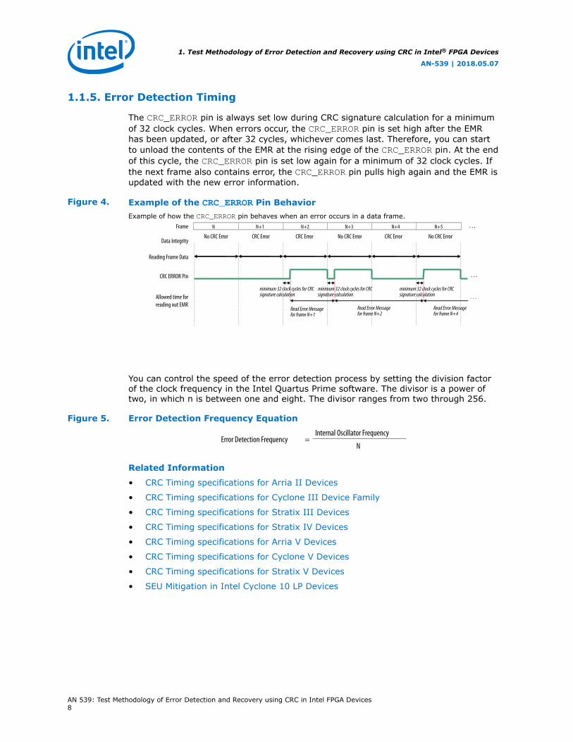
1.1.5. Error Detection Timing
The CRC_ERROR pin is always set low during CRC signature calculation for a minimumof 32 clock cycles. When errors occur, the CRC_ERROR pin is set high after the EMRhas been updated, or after 32 cycles, whichever comes last. Therefore, you can startto unload the contents of the EMR at the rising edge of the CRC_ERROR pin. At the endof this cycle, the CRC_ERROR pin is set low again for a minimum of 32 clock cycles. Ifthe next frame also contains error, the CRC_ERROR pin pulls high again and the EMR isupdated with the new error information.
Figure 4. Example of the CRC_ERROR Pin BehaviorExample of how the CRC_ERROR pin behaves when an error occurs in a data frame.
…
…
… N N+3N+1 N+2 N+4 N+5Frame
Data Integrity
Reading Frame Data
CRC ERROR Pin
Allowed time forreading out EMR
No CRC Error No CRC ErrorNo CRC ErrorCRC Error CRC Error CRC Error
minimum 32 clock cycles for CRCsignature calculation
minimum 32 clock cycles for CRCsignature calculation
minimum 32 clock cycles for CRCsignature calculation
Read Error Messagefor frame N+1
Read Error Messagefor frame N+2
Read Error Messagefor frame N+4
You can control the speed of the error detection process by setting the division factorof the clock frequency in the Intel Quartus Prime software. The divisor is a power oftwo, in which n is between one and eight. The divisor ranges from two through 256.
Figure 5. Error Detection Frequency Equation
Error Detection Frequency =Internal Oscillator Frequency
N
Related Information
• CRC Timing specifications for Arria II Devices
• CRC Timing specifications for Cyclone III Device Family
• CRC Timing specifications for Stratix III Devices
• CRC Timing specifications for Stratix IV Devices
• CRC Timing specifications for Arria V Devices
• CRC Timing specifications for Cyclone V Devices
• CRC Timing specifications for Stratix V Devices
• SEU Mitigation in Intel Cyclone 10 LP Devices
1. Test Methodology of Error Detection and Recovery using CRC in Intel® FPGA Devices
AN-539 | 2018.05.07
AN 539: Test Methodology of Error Detection and Recovery using CRC in Intel FPGA Devices8

1.2. Error Correction
In addition to error detection capability, Arria V, Cyclone V, and Stratix V devices alsosupport internal scrubbing. Internal scrubbing has the ability to internally correct softerrors. This is done on a per frame basis. Internal scrubbing corrects errors withoutthe need of reconfiguring the device. Internal scrubbing operates in user mode. Enablethe internal scrubbing feature in the Intel Quartus Prime software by turning on theEnable internal scrubbing option under the Error Detection CRC page in the Device& Pin Options dialog box.
Figure 6. Internal Scrubbing Feature
Error DetectionState Machine
32-Bit CRC Calculation andError Search Engine
Internal Scrubbing Data registers, CRC registers,and CRAM array
1.3. Using the Error Detection CRC Feature
To determine the location of the CRC errors, unload the EMR. You can shift thecontents of the EMR through the JTAG instruction or core interface.
1.3.1. Error Detection using User Logic
This section describes how to use the error detection feature through user logic with adesign example.
Related Information
• Design Example for Arria II, Stratix III, and Stratix IV Devices
• Design Example for Arria V, Cyclone V, and Stratix V Devices
1.3.1.1. Detecting CRC Errors through the CRC_ERROR Output Signal
To detect CRC errors through the CRC_ERROR output signal, use the CRC_ERRORoutput signal. Check whether a CRC error has been found in the CRC calculationbefore unloading the contents of the EMR. To do this, route the crcerror port fromthe WYSIWYG atom to the dedicated CRC_ERROR pin or any user I/O. To route thecrcerror port to a user I/O, you must insert a D flipflop (DFF) in between thecrcerror port and the user I/O.
1.3.1.2. Unloading the EMR through User Logic
To unload the EMR through user logic, establish an interface between the user logicand the error detection circuit using the WYSIWYG atom. The WYSIWYG atomprovides access to the error detection block. In addition, you must design a user logiccontrol block to control the necessary control signals to access the WYSIWYG atom.
1. Test Methodology of Error Detection and Recovery using CRC in Intel® FPGA Devices
AN-539 | 2018.05.07
AN 539: Test Methodology of Error Detection and Recovery using CRC in Intel FPGA Devices9

Figure 7. Interface Between the User Logic Control Block and the WYSIWYG Atom
SHIFTnLD
ED_CLK
CRC_Error
Regout
Clk_in
Start_write
User Logic Control Block
CRC Block WYSIWYG Atom
Note: WYSIWYG is a technique that performs optimization on the Verilog Quartus Mappingnetlist within the Intel Quartus Prime software.
1.3.1.3. Accessing the Error Detection Block through User Logic
Use the <device>_crcblock WYSIWYG component to establish the interface fromthe user logic to the error detection circuit. The <device>_crcblock primitive atomcontains the input and output ports that you must include in the atom. To access thelogic array, insert the <device>_crcblock WYSIWYG atom into your design.
You cannot use the information provided by the EMR to detect soft errors. Instead, usethe information provided by the CRC_ERROR output signal because it is not affected bysoft errors.
Figure 8. User Logic Error Detection Block DiagramFigure shows the error detection feature and the WYSIWYG atom that you must enable in your design.
Clock Di vider(1 to 256 Factor)
Pre-Comp uted CRC(Sa ved in the Option Register)
CRCComp utation
Error DetectionLogic
SRAMBits
CRC_ERROR(Sho wn in BIDIR Mode)
VCC
Logic Array
clk
shift
nld
rego
ut
crcer
ror
100 MHz or 80 MHz Internal Chip Oscillator
Note: For the Intel Quartus Prime software version 8.0 SP1 or earlier, you must enable theerror detection CRC feature in the Device & Pin Options dialog box in the Intel QuartusPrime software when you include the <device>_crcblock WYSIWYG atom in yourdesign.
1. Test Methodology of Error Detection and Recovery using CRC in Intel® FPGA Devices
AN-539 | 2018.05.07
AN 539: Test Methodology of Error Detection and Recovery using CRC in Intel FPGA Devices10

To enable the <device>_crcblock WYSIWYG atom, name the atom for each deviceaccordingly. For example, the WYSIWYG atom for the Stratix III device isstratixiii_crcblock and the Arria II device is arriaii_crcblock.
Table 4. CRC Block Input and Output PortsTable lists the input and output ports that you must include in the WYSIWYG atom.
Port Input/Output Definition
<crcblock_name> Input Unique identifier for the CRC block and represents any identifier name thatis legal for the given description language, such as the Verilog HDL, VHDL,and Altera Hardware Description Language (AHDL). This is a required field.
.clk(<clock source>) Input Designates the clock input of this cell. All operations of this cell are withrespect to the rising edge of the clock. Whether loading data into the cellor out of the cell, this always occurs on the rising edge. This is a requiredport.
.shiftnld (<shiftnldsource>)
Input • An input into the error detection block.• If shiftnld=1, the user shift register shifts the data to the regout
port at each rising edge of the clk port.• If shiftnld=0, the user shift register parallel loads the contents of
the user update register. This is a required port.• This input triggers clock enable for the user update register to de-
assert after two EDCLK cycles. After driving the ED_SHIFTNLD signallow, wait at least two EDCLK cycles before clocking the ED_CLK signal.
.crcerror (<crcerrorout destination>)
Output • Output of the cell that is synchronized to the internal oscillator of thedevice (100-MHz or 80-MHz internal oscillator) and not to the clkport. This output asserts automatically high if the error block detectsthat a SRAM bit has flipped and the internal CRC computation hasshown a difference with respect to the pre-computed value.
• Connect this signal to an output pin or a bidirectional pin. If youconnect this output signal to an output pin, you can only monitor theCRC_ERROR pin (the core logic cannot access this output). If the corelogic uses the CRC_ERROR signal to read the error detection logic,connect this signal to a BIDIR pin. The signal is fed to the coreindirectly by feeding a BIDIR pin that has its output enable port (oe)connected to VCC.
• The signal that is routed to the CRC_ERROR pin is also routed to thecore.
.regout(<outputdestination>)
Output • Output of the user shift register synchronized to the clk port, to beread by the core logic.
• This shifts one bit at each cycle and follows the LSB-first format.
Example 1. Example of the Input and Output Ports of a WYSIWYG Atom in a Stratix IIIDeviceExample shows the input and output ports of a WYSIWYG atom in a Stratix III device.
stratixiii_crcblock <crcblock_name>(.clk(<clock source>),.shiftnld(<shiftnld source>),.crcerror(<crcerror out destination>),.regout(<output destination>));defparam crc_wysiwyg_atom.oscillator_divider = 2
Note: The crc_wysiwyg_atom.oscillator_divider parameter describes the clockdivider for the error detection frequency of the <device>_crcblock WYSIWYGatom.
1. Test Methodology of Error Detection and Recovery using CRC in Intel® FPGA Devices
AN-539 | 2018.05.07
AN 539: Test Methodology of Error Detection and Recovery using CRC in Intel FPGA Devices11
Related Information
Error Detection Timing on page 8
1.3.1.4. User Logic Control Block
You define the user logic control block. A design example is provided with thisapplication note. In this design example, the user logic control block controls the inputport to the WYSIWYG atom to read out the contents of the user update register. Theuser update register is updated with the contents of the EMR. To read out the contentsof the user update register, follow these steps:
1. Drive the SHIFTnLD signal low.
2. Wait at least two ED_CLK cycles.
3. Clock Clk_in one cycle for one rising edge to load the contents of the userupdate register to the user shift register.
4. Drive the SHIFTnLD signal high.
5. Clock Clk_in 29 cycles to read out 30 bits of the error location information.
6. Clock Clk_in an additional 16 cycles to read out the syndrome of the error.
1.3.1.5. User Logic Control Block Signals
Table 5. User Logic Control Block Signals
Signal Name Input/Output
Description
clk_in Input Clock source to the user logic control block.
Start_write Input This input triggers the user logic control block to start driving the SHIFTnLD andED_CLK output signals. When this input is high, the user logic control blockstarts to run the mechanism to unload the user update register. This input isusually tied to the crcerror output port from the WYSIWYG atom because theEMR is unloaded at the rising edge of the crcerror port.
SHIFTnLD Output Output to the WYSIWYG atom. Use this signal to drive the shiftnld port of theWYSIWYG atom.
ED_CLK Output Output clock to the WYSIWYG atom. Use this clock as the clock source for theWYSIWYG atom. This clock is connected to the clk port of the WYSIWYG atom.The source of this clock comes from the clk_in input signal.
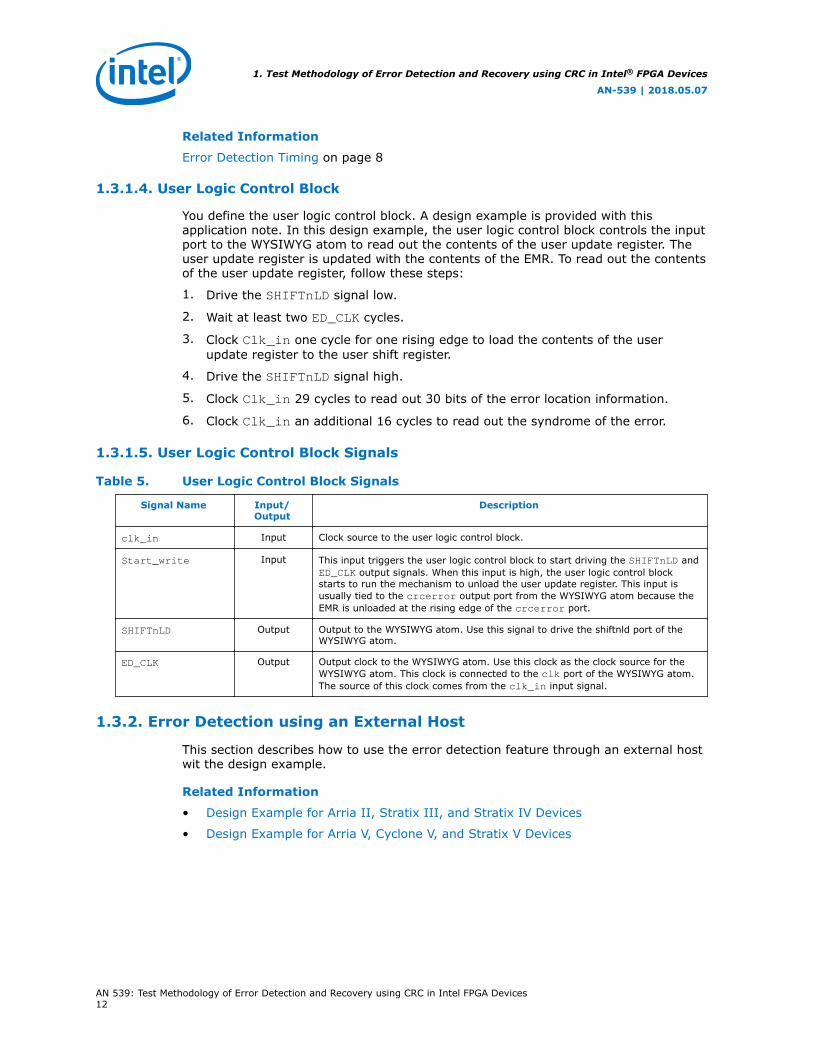
1.3.2. Error Detection using an External Host
This section describes how to use the error detection feature through an external hostwit the design example.
Related Information
• Design Example for Arria II, Stratix III, and Stratix IV Devices
• Design Example for Arria V, Cyclone V, and Stratix V Devices
1. Test Methodology of Error Detection and Recovery using CRC in Intel® FPGA Devices
AN-539 | 2018.05.07
AN 539: Test Methodology of Error Detection and Recovery using CRC in Intel FPGA Devices12

1.3.2.1. Detecting a CRC Error through the CRC_ERROR Output Signal
Before unloading the contents of the EMR, use the CRC_ERROR output signal to checkwhether a CRC error has been found throughout the CRC calculation. To do this,enable the error detection CRC feature in the Device & Pin Options dialog box in theIntel Quartus Prime software and observe the dedicated CRC_ERROR pin.
1.3.2.2. Unloading the EMR using an External Host
To unload the contents of the EMR using an external host, such as a JTAG port, usethe SHIFT_EDERROR_REG JTAG instruction. This JTAG instruction connects the EMR tothe JTAG pin in the error detection block between the TDI and TDO pins. You canexecute the instruction whenever the CRC_ERROR pin goes high.
You must unload the contents of the EMR before the register is overwritten by theinformation of the next CRC error.
The following examples show the Jam™ Standard Test and Programming Language(STAPL) Format File (.jam) used to execute the SHIFT_EDERROR_REG JTAGinstruction to unload the contents of the EMR.
Example 2. Example of .jam File to Unload the Contents of the EMR for Arria II, StratixIII, and Stratix IV Devices
ACTION UNLOAD_EMR = EXECUTE;
DATA EMR_DATA;
BOOLEAN out[46];
BOOLEAN in[46]=$3FFFFFFFFFFF;
ENDDATA;
PROCEDURE EXECUTE USES EMR_DATA;
DRSTOP IDLE;
IRSTOP IDLE;
STATE IDLE;
IRSCAN 10, $017;
WAIT IDLE, 10 CYCLES, 1 USEC, IDLE;
DRSCAN 46, in[45..0], CAPTURE out[45..0];
WAIT IDLE, 10 CYCLES, 25 USEC, IDLE;
PRINT " ";
PRINT "Data read out from the EMR Register: ", out[45], out[44], out[43], out[42], out[41], out[40], out[39], out[38], out[37], out[36], out[35], out[34], out[33], out[32], out[31], out[30]," ", out[29], out[28], out[27], out[26], out[25], out[24], out[23], out[22], out[21], out[20], out[19], out[18], out[17], out[16]," ", out[15], out[14], out[13], out[12], out[11], out[10], out[9], out[8], out[7], out[6], out[5]," ", out[4], out[3], out[2]," ", out[1], out[0];
PRINT " ";
PRINT "Syndrome:", out[45], out[44], out[43], out[42], out[41], out[40], out[39], out[38], out[37], out[36], out[35], out[34], out[33], out[32],
1. Test Methodology of Error Detection and Recovery using CRC in Intel® FPGA Devices
AN-539 | 2018.05.07
AN 539: Test Methodology of Error Detection and Recovery using CRC in Intel FPGA Devices13

out[31], out[30];
PRINT "Frame Address:", out[29], out[28], out[27], out[26], out[25], out[24], out[23], out[22], out[21], out[20], out[19], out[18], out[17], out[16];
PRINT "Byte Location:", out[15], out[14], out[13], out[12], out[11], out[10], out[9], out[8], out[7], out[6], out[5];
PRINT "Bit Location:", out[4], out[3], out[2];
PRINT "Error Type:", out[1], out[0];
STATE IDLE;
EXIT 0;
ENDPROC;
Example 3. Example of .jam File to Unload the Contents of the EMR for Arria V, CycloneV, and Stratix V Devices
ACTION UNLOAD_EMR = EXECUTE;
DATA EMR_DATA;
BOOLEAN out[67];
BOOLEAN in[67]=$7FFFFFFFFFFFFFFFF;
INTEGER i;
ENDDATA;
PROCEDURE EXECUTE USES EMR_DATA;
DRSTOP IDLE;
IRSTOP IDLE;
STATE IDLE;
IRSCAN 10, $017;
WAIT IDLE, 10 CYCLES, 1 USEC, IDLE;
DRSCAN 67, in[66..0], CAPTURE out[66..0];
WAIT IDLE, 10 CYCLES, 25 USEC, IDLE;
PRINT " ";
PRINT "Data read out from the ";
PRINT "EMR_Register ::", out[66], out[65], out[64], out[63], out[62], out[61], out[60], out[59], out[58], out[57], out[56], out[55], out[54], out[53], out[52], out[51], out[50], out[49], out[48], out[47], out[46], out[45], out[44], out[43], out[42], out[41], out[40], out[39], out[38], out[37], out[36], out[35]," ", out[34], out[33], out[32], out[31], out[30], out[29], out[28], out[27], out[26], out[25], out[24], out[23], out[22], out[21], out[20], out[19]," ", out[18], out[17], out[16], out[15], out[14], out[13], out[12], out[11], out[10], out[9]," ", out[8], out[7]," ", out[6], out[5], out[4]," ", out[3], out[2], out[1], out[0];
'PRINT " ";
PRINT "Syndrome ::", out[66], out[65], out[64], out[63], out[62], out[61], out[60], out[59], out[58], out[57], out[56], out[55], out[54], out[53], out[52], out[51], out[50], out[49], out[48], out[47], out[46], out[45], out[44], out[43], out[42], out[41], out[40], out[39], out[38], out[37],
1. Test Methodology of Error Detection and Recovery using CRC in Intel® FPGA Devices
AN-539 | 2018.05.07
AN 539: Test Methodology of Error Detection and Recovery using CRC in Intel FPGA Devices14

out[36], out[35];
PRINT "Frame Address ::", out[34], out[33], out[32], out[31], out[30], out[29], out[28], out[27], out[26], out[25], out[24], out[23], out[22], out[21], out[20], out[19];
PRINT "Double Word Location ::", out[18], out[17], out[16], out[15], out[14], out[13], out[12], out[11], out[10], out[9];
PRINT "Byte Offset ::", out[8], out[7];
PRINT "Bit Offset ::", out[6], out[5], out[4];
PRINT "Error Type ::", out[3], out[2], out[1], out[0];
STATE IDLE;
EXIT 0;
ENDPROC;
Related Information
Error Message Register on page 6
1.4. Error Injection
To test the error detection block, you can intentionally inject errors. This errorinjection methodology provides design verification and system fault tolerancecharacterization. Using the EDERROR_INJECT JTAG instruction, you can inject a singleerror, double errors, or double-adjacent errors to the configuration memory.
Table 6. EDERROR_INJECT JTAG Instruction
JTAG Instruction Instruction Code Description
EDERROR_INJECT 00 0001 0101 This instruction controls the 21-bit JTAG fault injection register thatis used for error injection.
Note: For Stratix V III devices, you can only execute the EDERROR_INJECT JTAG instructionat a 50 MHz error detection frequency. Refer related information below.
Related Information
SEU Mitigation in Stratix III Devices
1.4.1. Fault Injection Register
The EDERROR_INJECT JTAG instruction controls the contents of the JTAG faultinjection register. The register holds the information of the error that you want toinject into the configuration memory.
You can scan the location of the error or errors into the 21-bit (46-bit for Arria V,Cyclone V, and Stratix V devices) JTAG fault injection register at any time. Thecontents of the JTAG fault injection register is loaded into the fault injection registerwhen the last and first data frame is being processed. In other words, you can onlyinject the error into the first frame of the configuration data but you can monitor theerror information at any time.ister holds the information of the error that you want toinject into the configuration memory.
1. Test Methodology of Error Detection and Recovery using CRC in Intel® FPGA Devices
AN-539 | 2018.05.07
AN 539: Test Methodology of Error Detection and Recovery using CRC in Intel FPGA Devices15
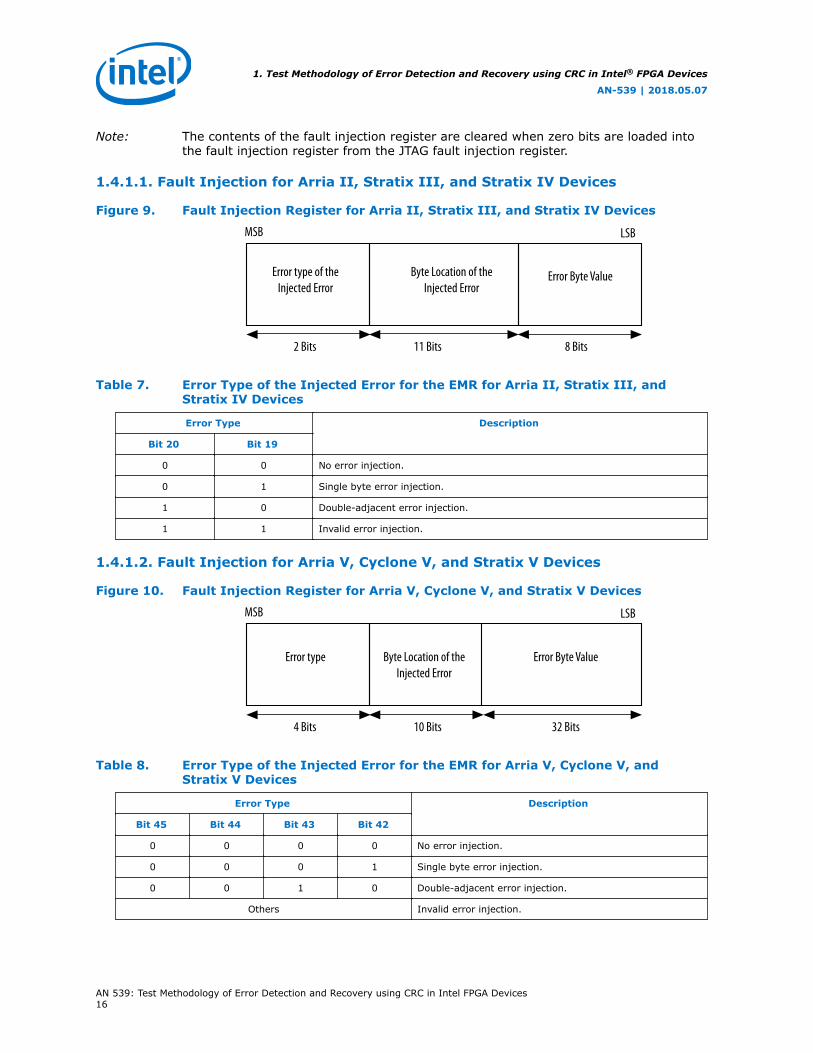
Note: The contents of the fault injection register are cleared when zero bits are loaded intothe fault injection register from the JTAG fault injection register.
1.4.1.1. Fault Injection for Arria II, Stratix III, and Stratix IV Devices
Figure 9. Fault Injection Register for Arria II, Stratix III, and Stratix IV Devices
MSB LSB
Error type of the Injected Error
Byte Location of the Injected Error
Error Byte Value
2 Bits 11 Bits 8 Bits
Table 7. Error Type of the Injected Error for the EMR for Arria II, Stratix III, andStratix IV Devices
Error Type Description
Bit 20 Bit 19
0 0 No error injection.
0 1 Single byte error injection.
1 0 Double-adjacent error injection.
1 1 Invalid error injection.
1.4.1.2. Fault Injection for Arria V, Cyclone V, and Stratix V Devices
Figure 10. Fault Injection Register for Arria V, Cyclone V, and Stratix V Devices
MSB LSB
Error type Byte Location of the Injected Error
Error Byte Value
4 Bits 10 Bits 32 Bits
Table 8. Error Type of the Injected Error for the EMR for Arria V, Cyclone V, andStratix V Devices
Error Type Description
Bit 45 Bit 44 Bit 43 Bit 42
0 0 0 0 No error injection.
0 0 0 1 Single byte error injection.
0 0 1 0 Double-adjacent error injection.
Others Invalid error injection.
1. Test Methodology of Error Detection and Recovery using CRC in Intel® FPGA Devices
AN-539 | 2018.05.07
AN 539: Test Methodology of Error Detection and Recovery using CRC in Intel FPGA Devices16

1.4.2. Error Injection using the EDERROR_INJECT JTAG Instruction
This section describes the testing process. When using a .jam file to automate thetesting process, you can test and verify the functionality of the error detection blockwithout having to reconfigure the device. Use the EDERROR_INJECT JTAG instructionto control the contents of the JTAG fault injection register to flip the readback bits of aparticular location in the first data frame as specified in the JTAG fault injectionregister.
Note: Intel recommends observing the behavior of the CRC_ERROR pin and unloading thecontents of the EMR using the recommended approaches to verify the error has beencorrectly injected.
1.4.2.1. Injecting Single-Bit Error for Arria II, Stratix III, and Stratix IV
If you want to inject a single-bit error into the 7th bit of the 5th byte in the first dataframe, you must shift in the data that contains the information of the injected errorinto the fault injection register.
The following figure shows the binary bit sequence 0 1000 0000 0100 0100 0000 isshifted into the fault injection register. Because bit 19 and bit 20 of the fault injectionregister is 01, a single-bit error is injected. The byte location of the injected error isdefined as 000 0000 0100, thus the single-bit error is injected into the 5th byte of thedata frame. The error byte location value is 0100 0000, which indicates the 7th bit ofthe 5th byte data is the specific location in which the single-bit error is injected.
Figure 11. Injecting a Single-Bit Error for Arria II, Stratix III, and Stratix IV DevicesFigure shows the error injection mechanism.
FIR register content
Correct data in first data frame
Data in first data framewith single-bit error
MSB LSB
01 000 0000 0100 0100 0000
Byte 4 Byte 3 Byte 0
Byte 4 Byte 3 Byte 0
1100 0000 1010 0000 . . .
1000 0000 1010 0000 . . .
The following example shows the .jam file that you must execute in theEDERROR_INJECT JTAG instruction to inject the single-bit error into the first dataframe for Arria II, Stratix III, and Stratix IV devices.
1. Test Methodology of Error Detection and Recovery using CRC in Intel® FPGA Devices
AN-539 | 2018.05.07
AN 539: Test Methodology of Error Detection and Recovery using CRC in Intel FPGA Devices17

Example 4. Example of .jam File to Inject Single-Bit Error for Arria II, Stratix III, andStratix IV Devices
ACTION ERROR_INJECT = EXECUTE;
DATA DEVICE_DATA;
BOOLEAN out[21];
BOOLEAN in[21] = $080440;
ENDDATA;
PROCEDURE EXECUTE USES DEVICE_DATA;
BOOLEAN X = 0;
DRSTOP IDLE;
IRSTOP IDLE;
STATE IDLE;
IRSCAN 10, $015;
WAIT IDLE, 10 CYCLES, 1 USEC, IDLE;
DRSCAN 21, in[20..0], CAPTURE out[20..0]; ‘shift out the previous content from fault injection register
WAIT IDLE, 10 CYCLES, 1 USEC, IDLE;
DRSCAN 21, in[20..0], CAPTURE out[20..0]; ‘shift out current content from fault injection register
WAIT IDLE, 10 CYCLES, 25 USEC, IDLE;
PRINT " ";
PRINT "Data read out from the FIR Register: ", out[20], out[19], " " ,out[18], out[17], out[16], out[15], out[14], out[13], out[12], out[11], out[10], out[9], out[8], " " , out[7], out[6], out[5], out[4], out[3], out[2], " ", out[1], out[0];
PRINT " ";
PRINT "Error Type:", out[20], out[19];
PRINT " ";
PRINT "Byte Location:", out[18], out[17], out[16], out[15], out[14], out[13], out[12], out[11], out[10], out[9], out[8];
PRINT " ";
PRINT "Error Byte Value:", out[7], out[6], out[5], out[4], out[3], out[2], out[1], out[0];
STATE IDLE;
EXIT 0;
ENDPROC;
1. Test Methodology of Error Detection and Recovery using CRC in Intel® FPGA Devices
AN-539 | 2018.05.07
AN 539: Test Methodology of Error Detection and Recovery using CRC in Intel FPGA Devices18

1.4.2.2. Injecting Single-Bit Error for Arria V, Stratix V, and Cyclone V Devices
If you want to inject a single-bit error into the 15th bit of the 7th byte in the first dataframe, you must shift in the data that contains the information of the injected errorinto the fault injection register.
The following figure shows the binary bit sequence 00 0100 0000 0110 0000 00000000 0000 0100 0000 0000 0000 is shifted into the fault injection register. Becausebits 45, 44, 43, and 42 of the fault injection register is 0001, a single-bit error isinjected. The byte location of the injected error is defined as 00 0000 0110, thus thesingle-bit error is injected into the 7th byte of the data frame. The error byte locationvalue is 0000 0000 0000 000 0100 0000 0000 0000, which indicates the 15th bit ofthe 7th byte data is the specific location in which the single-bit error is injected.
Figure 12. Injecting a Single-Bit Error for Arria V, Stratix V, and Cyclone V DevicesFigure shows the error injection mechanism.
FIR register content
Correct data in first data frame
Data in first data framewith single-bit error
MSB LSB
00 0100 0000 0110 0000 0000 0000 0000 0100 0000 0000 0000
Byte 6 Byte 5 Byte 0
Byte 6 Byte 5 Byte 0
1000 0100 0010 0000 1100 0000 0000 0000 1010 0101 0000...
1000 0100 0010 0000 1000 0000 0000 0000 1010 0101 0000...
The following example shows the .jam file that you must execute in theEDERROR_INJECT JTAG instruction to inject the single-bit error into the first dataframe for Arria V, Stratix V, and Cyclone V devices.
Example 5. Example of .jam File to Inject Single-Bit Error for Arria V, Stratix V, andCyclone V Devices
ACTION ERROR_INJECT = EXECUTE;
DATA DEVICE_DATA;
BOOLEAN out[46];
BOOLEAN in[46] = $040600004000;
ENDDATA;
PROCEDURE EXECUTE USES DEVICE_DATA;
BOOLEAN X = 0;
DRSTOP IDLE;
1. Test Methodology of Error Detection and Recovery using CRC in Intel® FPGA Devices
AN-539 | 2018.05.07
AN 539: Test Methodology of Error Detection and Recovery using CRC in Intel FPGA Devices19

IRSTOP IDLE;
STATE IDLE;
IRSCAN 10, $015;
WAIT IDLE, 10 CYCLES, 1 USEC, IDLE;
DRSCAN 46, in[45..0], CAPTURE out[45..0]; ‘shift out the previous content from fault injection register
WAIT IDLE, 10 CYCLES, 1 USEC, IDLE;
DRSCAN 46, in[45..0], CAPTURE out[45..0]; ‘shift out current content from fault injection register
WAIT IDLE, 10 CYCLES, 50 USEC, IDLE;
PRINT " "; PRINT "Data read out from the FIR Register: ", out[45], out[44], out[43], out[42], " ", out[41], out[40], out[39], out[38], out[37], out[36], out[35], out[34], out[33], out[32], " ", out[31], out[30], out[29], out[28], out[27], out[26], out[25], out[24], out[23], out[22], out[21], out[20], out[19], out[18], out[17], out[16], out[15], out[14], out[13], out[12], out[11], out[10], out[9], out[8], out[7], out[6], out[5], out[4], out[3], out[2], out[1], out[0];
PRINT " ";
PRINT "Error Type:", out[45], out[44], out[43], out[42];
PRINT " ";
PRINT "Byte Location:", out[41], out[40], out[39], out[38], out[37], out[36], out[35], out[34], out[33], out[32];
PRINT " ";
PRINT "Error Byte Value:", out[31], out[30], out[29], out[28], out[27], out[26], out[25], out[24], out[23], out[22], out[21], out[20], out[19], out[18], out[17], out[16], out[15], out[14], out[13], out[12], out[11], out[10], out[9], out[8], out[7], out[6], out[5], out[4], out[3], out[2], out[1], out[0];
STATE IDLE;
EXIT 0;
ENDPROC;
1.4.3. Clearing Fault Injection Register
After completing the test process, clear the contents of the fault injection register orstart a reconfiguration by pulling the nCONFIG signal low to disable the error that youinjected. To clear the contents of the fault injection register, scan all zero data into theregister.
The following example shows a .jam file used to clear the contents of the faultinjection register.
Example 6. Example of .jam File to Clear the Contents of the Fault Injection Register
ACTION ERROR_INJECT_DISABLE = EXECUTE;
DATA DEVICE_DATA;
BOOLEAN out[21];
1. Test Methodology of Error Detection and Recovery using CRC in Intel® FPGA Devices
AN-539 | 2018.05.07
AN 539: Test Methodology of Error Detection and Recovery using CRC in Intel FPGA Devices20

BOOLEAN in[21] = $000000;
ENDDATA;
PROCEDURE EXECUTE USES DEVICE_DATA;
BOOLEAN X = 0;
DRSTOP IDLE;
IRSTOP IDLE;
STATE IDLE;
IRSCAN 10, $015;
WAIT IDLE, 10 CYCLES, 1 USEC, IDLE;
DRSCAN 21, in[20..0], CAPTURE out[20..0]; ‘shift out the previous content from fault injection register
WAIT IDLE, 10 CYCLES, 1 USEC, IDLE;
DRSCAN 21, in[20..0], CAPTURE out[20..0]; ‘shift out current content from fault injection register
WAIT IDLE, 10 CYCLES, 25 USEC, IDLE;
PRINT " ";
PRINT "Data read out from the FIR Register: ", out[20], out[19]," " , out[18], out[17], out[16], out[15], out[14], out[13], out[12], out[11], out[10], out[9], out[8], " ", out[7], out[6], out[5], out[4], out[3], out[2], out[1], out[0];
PRINT " ";
PRINT "Error Type:", out[20], out[19];
PRINT " ";
PRINT "Byte Location:", out[18], out[17], out[16], out[15], out[14], out[13], out[12], out[11], out[10], out[9], out[8];
PRINT " ";
PRINT "Error Byte Value:", out[7], out[6], out[5], out[4], out[3], out[2], out[1], out[0];
STATE IDLE;
EXIT 0;
ENDPROC;
Note: Intel recommends reconfiguring the device after error detection testing andverification.
1. Test Methodology of Error Detection and Recovery using CRC in Intel® FPGA Devices
AN-539 | 2018.05.07
AN 539: Test Methodology of Error Detection and Recovery using CRC in Intel FPGA Devices21

1.5. Document Revision History for AN 539: Test Methodology ofError Detection and Recovery using CRC in Intel FPGA Devices
DocumentVersion
Changes
2018.05.07 • Rebranded to Intel.• Updated Examples:
— Example of .jam File to Inject Single-Bit Error for Arria II, Stratix III, and Stratix IV Devices— Example of .jam File to Inject Single-Bit Error for Arria V, Cyclone V, and Stratix V Devices— Example of .jam File to Clear the Contents of the Fault Injection Register
Date Version Changes
June 2017 2017.06.14 Corrected Example 5.
August 2016 2016.08.03 • Corrected Fault Injection Register sub-section title.
August 2015 2015.08.20 • Fixed editorial error in Fault Injection Register.• Fixed Related links descriptions.• Removed link to an application note for mature products, AN357.
May 2015 2015.05.04 • Updated Example of .jam File to Inject Single-Bit Error for Arria V,Cyclone V and Stratix V Devices by correcting double quotation typeand added semicolon in line 35.
• Template update.
December 2014 2014.12.15 • Updated Figure 3 on page 5.
April 2014 3.0 • Updated Table 5 on page 11 to correct the .clk(<clock source>) portoperation from falling edge to rising edge of the clock.
• Updated document to support Arria V and Cyclone V.• Updated Figure 3 on page 5.• Added Example 3 on page 16.
June 2011 2.0 • Added Figure 3, Figure 10, and Figure 12.• Added Table 4 and Table 9.• Added Example 5.• Added the “Error Correction” section.• Updated Figure 1, Figure 2, Figure 9, and Figure 11.• Updated Table 1, Table 3, and Table 8.• Updated the “Functional Description”, “Configuration Error Detection”,
“User Mode Error Detection”, “Error Message Register”, “FaultInjection Register”, and “Error Injection using the EDERROR_INJECTJTAG Instruction” sections.
• Minor text edits.
April 2009 1.1 • Updated the “Introduction”, “Error Injection using EDERROR_INJECTJTAG Instruction”, “Error Injection”, and “Error Detection Pin”sections.
• Updated Table 4 and Table 8.
December 2008 1.0 Initial release.
1. Test Methodology of Error Detection and Recovery using CRC in Intel® FPGA Devices
AN-539 | 2018.05.07
AN 539: Test Methodology of Error Detection and Recovery using CRC in Intel FPGA Devices22