a review on 3d micro-additive manufacturing technologies
TRANSCRIPT

ORIGINAL ARTICLE
A review on 3D micro-additive manufacturing technologies
Mohammad Vaezi & Hermann Seitz & Shoufeng Yang
Received: 27 June 2011 /Accepted: 30 October 2012 /Published online: 25 November 2012# Springer-Verlag London 2012
Abstract New microproducts need the utilization of a di-versity of materials and have complicated three-dimensional(3D) microstructures with high aspect ratios. To date, manymicromanufacturing processes have been developed butspecific class of such processes are applicable for fabricationof functional and true 3D microcomponents/assemblies. Theaptitude to process a broad range of materials and the abilityto fabricate functional and geometrically complicated 3Dmicrostructures provides the additive manufacturing (AM)processes some profits over traditional methods, such aslithography-based or micromachining approaches investi-gated widely in the past. In this paper, 3D micro-AM pro-cesses have been classified into three main groups,including scalable micro-AM systems, 3D direct writing,and hybrid processes, and the key processes have beenreviewed comprehensively. Principle and recent progressof each 3D micro-AM process has been described, and theadvantages and disadvantages of each process have beenpresented.
Keywords Additive manufacturing (AM) . Direct writing(DW) .Microelectromechanical systems (MEMS) . Rapidmicromanufacturing
1 Introduction
Nowadays, there is an enormous variety in microproducts,the major kinds being microelectromechanical systems(MEMS), micro-opto-electro-mechanical systems(MOEMS), and microelectronic products and micro-opticalelectronics systems (MOES) depending on the mixtures ofproduct usefulness and operation fundamentals [197]. Dueto the present tendency towards miniaturization of productsin many industries comprising medical, automotive, optics,electronics, and biotechnology sectors [4], there is a demandfor improvements in micro- and nanofabrication technolo-gies and merging them in new manufacturing platforms.
A broad range of microfabrication technologies have beendeveloped which have different applications and capabilitiesas their fundamentals are very diverse. Several classificationschemes have been suggested by researchers to categorizemicrofabrication techniques. Masuzawa [171] focused onmicromachining processes and classified them according tothe implemented machining approach. Madou [167] catego-rized the microfabrication techniques as lithographic and non-lithographic methods. Perhaps the most widespreadclassification is that of Brinksmeier et al. [24] and Brousseauet al. [26] in which micromanufacturing has been classified intwo generic technology groups: microsystem technologies(MST) and microengineering technologies (MET). MST en-compass the processes for the manufacture of MEMS andMOEMS while MET cover the processes for the productionof highly precise mechanical components, moulds, and micro-structured surfaces. An alternative classification was sug-gested by Dimov et al. [59] in which micromanufacturingtechnologies have been categorized according to their process“dimension” and material relevance.
Microfabrication technologies can also be categorizedcorrespondingly as MEMS manufacturing and non-MEMSmanufacturing [198]. MEMS manufacturing includes
M. Vaezi (*) : S. YangEngineering Materials Group, Engineering Sciences,Faculty of Engineering and the Environment,University of Southampton,Southampton SO17 1BJ, UKe-mail: [email protected]
H. SeitzFluid Technology and Microfluidics,University of Rostock,Rostock 18059, Germany
Int J Adv Manuf Technol (2013) 67:1721–1754DOI 10.1007/s00170-012-4605-2

widely methods, such as laser ablation; plating; photolithog-raphy; lithography, electroplating, and molding (LIGA—German acronym); chemical etching; etc. Non-MEMS man-ufacturing generally includes methods, such as microextru-sion, laser patterning/cutting/drilling, EDM, microinjectionmolding, microembossing, microstamping, micromechani-cal cutting, etc. [197]. Also depending on the used materials,microfabrication technologies are categorized as silicon-based and nonsilicon material microfabrication.
Many microfabrication processes have been developed upto the present, but such techniques are restricted when utilizedto new microproducts which need the employment of a diver-sity of materials and have complicated three-dimensional (3D)microstructures with high aspect ratios. Recently, there hasbeen fast improvement in micromanufacturing of 3D micro-structures utilizing different methods and materials.Manufacturing technologies for 3D microcomponents play animportant role in various areas of modern technologies in theevolvement of very functional applications such as biochips,MEMS, microfluidic devices, photonic crystals, etc. [138,144]. In MEMS technology, demand for fabricating complexmicrostructures from wide range of materials such as ceramics,metals, polymers, and semiconductor materials is observed.
MEMS technology will improve substantially if morecomplicated 3D microstructures can be created to fabricateintegrated microsensors, medical devices, or micro-opticalsystems. Especially, fabrication of 3D microcomponents/assemblies which involve moving parts is a great challengein micromechanics field. Some micromanufacturing meth-ods such as soft lithography [259], laser photoablation[178], localized electrochemical deposition [166], theLIGA process [17, 69], etc., have been developed to pro-mote the ability of the technology for more complicatedmicrostructures. The LIGA process uses masked X-ray/laserradiation to incorporate thick resist layers to fabricate highaspect ratio microparts [11]. The LIGA process is restrictedin producing 2.5D microparts and manufacture of complex3D microstructure was still a challenge. Several processeshave been examined for solving the critical problem of 3Dmicromanufacturing. In this way, the electrochemical fabri-cation (EFAB) process has been developed as an improvedLIGA process to produce complicated 3D metal micropartslayer by layer [47, 50]. Different 3D microparts can beproduced using these methods from engineering materials,but majority of the processes (except EFAB) were devel-oped for 2.5D micromanufacturing, which does not have theaptitude to produce a perfect and real 3D microparts.Multilayered photolithography [238] and deep proton writ-ing [55, 240] were results of some earlier attempts towardtrue 3D microfabrication. New approaches such as micro-additive manufacturing (micro-AM) can also be consideredto enhance capability of microfabrication technology in true3D microcomponents manufacturing area.
2 Description and classification of 3D micro-AM
Among attainable alternatives, additive manufacturing(AM) processes that are based on layer-by-layer manu-facturing are identified as an effective method to attaintrue 3D microproducts. 3D micro-AM can be classifiedinto three main groups, including: scalable AM technol-ogies which can be employed for both macro- andmicroscale, 3D direct writing (3DDW) technologieswhich have been merely developed for microscale andhybrid processes (Fig. 1).
AM technologies have been widely utilized within adecade with the purpose of producing complicated 3D com-ponents. Fabrication of 3D microparts/structures is alsowithin the reach of some specific AM technologies viaimplementation of some essential modifications andimprovements to get proper conditions for microfabrication.Scalable AM technologies, including: stereolithography(SL; which is called micro-SL (MSL) in microscale), selec-tive laser sintering (SLS; which is called microlaser sinter-ing (MLS) in microscale), 3D printing (3DP), inkjet printingprocesses, fused deposition modelling (FDM), and laminat-ed object manufacturing (LOM) are the first group of thetechnology which have been regarded as a promising ap-proach for true 3D micromanufacturing and can beemployed efficiently to fabricate complex 3D microcompo-nents/assemblies. However, this class of micro-AM systems(except MSL) still suffers by some difficulties for micro-scale manufacturing as AM technologies have been devel-oped mainly for normal-size fabrication. Some limitations ofthis group are due to its temperament and are same for bothnormal- and microsize manufacturing but some other limi-tations are for adaptation of this group for microsizemanufacturing.
The second group of 3D micro-AM processes is 3DDWtechnologies. DW technologies have been developed basi-cally for two-dimensional (2D) writing but some of DWmethods such as laser chemical vapor deposition (LCVD),focused ion beam (FIB)DW, aerosol jet process, laser-induced forward transfer (LIFT), matrix-assisted pulsed-laser direct write (MAPLE), and nozzle dispensing process-es (including precision pump and syringe-based depositionmethods) can be utilized (or have potential) to produce high-resolution 3D microstructures/components. Among DWtechnologies, 3D-LCVD and FIBDW are used more effi-ciently to produce 3D microstructures. Nozzle dispensingtechniques are currently used to produce 3D microperiodicstructures for different applications. Aerosol jet process isserved less for microfabrication of true 3D microstructures,but it has high potential for use in 3D applications. Someother DW approaches, such as LIFT and MAPLE can beused in a layer-by-layer process to build 3D structures, butthey are still under development for micro-3D applications
1722 Int J Adv Manuf Technol (2013) 67:1721–1754

and a few research works have been reported on this issue.Overall, DW technologies need more improvements to be-come more compatible with 3D microfabrication, as most ofDW methods have been developed normally for 2Dpurposes.
Hybrid processes including shape deposition modelling(SDM) and EFAB can be classified as the third group of the3D micro-additive technologies. EFAB process uses elec-trochemical deposition and subtractive planarization in alayer-by-layer process to build 3D microstructures, whileSDM process utilizes additive and subtractive processessequentially to produce 3D microstructures. Among hybridprocesses, the EFAB process has shown great applicabilityfor true 3D micromanufacturing.
This paper presents a comprehensive review on the keymicro-AM processes which are currently used effectivelyfor true 3D microfabrication. Processes such as LIFT,MAPLE, aerosol jet, and SDM are not within the scope ofthis article since they are mostly employed for 2D/2.5Dfabrication at the moment, although they have capabilityof 3D microfabrication. In the meantime, different nozzledispensing DW techniques would be discussed along withFDM process (section 3.5) as they have same workingprinciple (all are based on material extrusion), although theyhave been classified as direct writing techniques. It shouldbe noted that the definitions from Madou [167] are accom-modated in this paper for micromanufacturing. In this way,micromanufacturing applies to the manufacturing of com-ponents/products where the dimensions of at least one fea-ture are in the micron scale.
3 Scalable AM processes
3.1 Stereolithography process
SL process is the first commercial AM process developed by3D Systems Inc. and is based on layer-by-layer photosensitiveresin polymerization using ultraviolet (UV) light. MSL is anadditive 3D micromanufacturing process which was first intro-duced by Ikuta and Hirowatari [103] through developing theintegrated hardened (IH) polymer SL and the improved superIH process [104]. MSL is on the basis of conventional SL, inwhich a light source radiates UV laser beam on a surface of aUV-curable liquid photopolymer, bringing about solidificationof the photopolymer. MSL has submicron resolution for the x,y, z translational stages, laser spot has smaller diameter (a fewmicrometers) compared with classical SL, photopolymer solid-ification occurs in a very small area of the resin layer by layerand thus MSL enables to produce microparts with 1–10 μm-layer thickness. This micro-additive process is used in variousareas such as micromachines and microsensors [218], micro-fluidic systems [105], optical waveguides [188], 3D photonicband gap structures [225], fluid chips for protein synthesis[275] and bio-analysis [19, 20]. Two main MSL techniques,namely, scanning MSL and projection MSL have been devel-oped depending on the different beam delivery system.
The scanning MSL solidify the photopolymer (includingUV photoinitiator, monomer, and other additives) in a point-by-point and line-by-line style in each layer. That was whyTakagi and Nakajima [235] called this process as “vector-by-vector”MSL. Focal length of the laser should be very short to
Fig. 1 Classification of 3D micro-AM processes
Int J Adv Manuf Technol (2013) 67:1721–1754 1723

reach laser spot sizes in a few micrometers. This results introubles for scanning the laser beam. Thus, in optimized scan-ningMSL, the laser spot is focused by a dynamic lens and thenthe resin vat has been moved in x, y, and z directions formoving the laser spot instead of low-inertia galvanometricmirror (as is utilized in classical SL), which causes defocusingproblem [103]. In this way, Xu et al. [261] developed ascanning MSL system with laser light spot with a diameter of12.89 μm on the focal plane and resin layers with a thicknessof 20 μm.
In projection MSL, build time is saved significantly com-pared with the scanningMSL as whole layer of the photopoly-mer is cured once via exposure through provided mask.However, the first generation of projection MSL systems wasslow and costly since a lot of projection masks had to beproduced. In 1994, Suzumori et al. [234] proposed a SLsystem which utilized glass photo mask for exposure. The ideaof mask-based MSL was ripened by Nakamoto andYamaguchi [186]. In 2000, refrigerated MSL was utilized tocreate mask patterns via drawing an individual sol–gel trans-formable resin. To overcome the troubles included in themultiple mask process, the dynamic mask was used insteadof multiple masks. The dynamic mask was used to electroni-cally create pattern projection for exposure, with no need toreplace the mask physically for each layer. In 1997, Bertsch etal. [19, 20] proposed that liquid crystal display (LCD) can beapplied as the dynamic mask to control the expected pattern ofeach layer in the projection SL process. In LCD projectors, anarray of light valves which is fabricated from liquid crystalmaterial is applied as a projector to control the on/off of theUVlight. Using LCD projectors caused reduction of the cost andsolved the difficulties by the glass mask alignment. Monneretet al. [182] promoted the LCD-basedMSL systems and Huanget al. [98] developed a LCD-based MSL system for directmask photocuring. In 2000, a thin film transistor LCD wasutilized by Hatashi [92] as a dynamic mask to produce opticallenses. Besides, the spatial light modulator as the dynamicmask and the UV light as the light source was used to intensifythe microfeatures of the photomask image in area-formingrapid prototyping [37]. Some inherent defects of the LCDmask projection are: low switching speed (∼20 ms), large pixelsizes, low filling ratio, low optical density of the refractiveelements during the off mode, and the higher light absorptionduring the on mode [230]. Such defects (specially, large pixelsize) restricted subsequent improvement of this technique formicromanufacturing.
Bertsch’s research group [12] proposed that the digitalmicromirror device (DMD) which is embedded in DigitalLight Processing projectors can be applied as the dynamicmask in MSL process. They used a metal halide lampcombined with optical filters to select a band of visiblewavelength for the irradiation of the resin. In 2004,Stampfl et al. [222] used DMD-based MSL, in which visible
light is projected from below the resin vat to produce high-quality 3D microparts. Furthermore, UV light was utilizedby Hadipoespito et al. [89] and Cheng et al. [39] instead ofvisible light, to cure the resin. The DMD is a semiconductorchip that has been developed by Texas Instruments® forhigh-quality digital projection. It involves many (around1.5 million) micromirrors (each side at ∼13 μm) which arepositioned in a matrix and each mounted on tiny hinges andcan be individually controlled. Each micromirror stands for1 pixel in the projected pattern and can be inclined autono-mously at a small angle (±10–12°) via an electrostatic forceto reflect the light and can repositioned quickly for turningthe light on and off. As the resolution of the projected imageis related to the size and number of the mirrors, high-resolution DMDs like 2,800×2,100 has been utilized inMSL to produce finer 3D microparts. To improve achiev-able resolution, DMD-based MSL systems are supplied withenhanced resolution module (ERM), whereby for each pixelbuilt there are two exposures, shifted by half a pixel, whichhalves the native resolution of the system [28]. Figure 2shows the difference between a standard DMD-based MSLand a DMD-based MSL supplied with ERM schematically.
The Perfactory is a DMD-based micro-SL system suppliedwith ERM which has been commercialized by envisionTECGmbH, Germany. The Perfactory system can build 3D micro-parts layer by layer (layer thickness down to 15 μm) withminimum pixel size of 30 μm using ERM module. Figure 3shows microparts with different blade thicknesses which havebeen fabricated in an experimental work by the authors withthe use of the Perfactory micro-SL system. The minimumpixel size of 30 μm can be observed in Fig. 3c.
Rapid microproduct development (RMPD) technologies isanother projection MSL which have been invented and interna-tional patented bymicroTECGesellschaft fürMikrotechnologiembH and the technologies are not based on US-patented DMD.It is possible to produce many microparts fast using microTECtechnologies and also realize a higher resolution layer-by-layer(as thin as 1μm) and surface quality in the sub-nanometer rangeusing RMPD-nanoface technology [82].
RMPD writing system uses parallel laser beams, whileRMPD mask uses UV light lambs and masks. In fact, RMPDmask is combination of mask technology used in photolithog-raphy and RMPD, which allows large-area exposure of thelayers, and a considerable reduction of exposure time.
Several dynamic mask MSL systems have been developedby researchers up to now through the great ability of thismicromanufacturing technology for fabricating complicated3D microparts/components and batch fabrication of 3DMicrosystems. Considerable attempts are also being made toemploy a wide range of materials in MSL process for fabrica-tion of MEMS with individual functions. In this way, differentmaterials such as ceramics and metals as well as photocurablepolymers have been utilized efficiently in MSL process [16,
1724 Int J Adv Manuf Technol (2013) 67:1721–1754

40]. Especially, some biodegradable photocurable polymershave been utilized successfully in drug delivery systems andtissue engineering (TE) [132, 138, 144]. The process of re-search on development ofMSL process has entered a new stagein a manner that efforts have been significantly increasedtoward optimization of process and its utility in new fields.Fabrication range is limited in MSL by the field of view ofpattern generator (LCD or DMD) and the magnification of theobjective lens. Ha et al. proposed a partitioned cross-sectionmethod for expanding the fabrication range while maintainingthe fabrication resolution [88] and improving accuracy in theprojectionMSL system [190]. Zhou and Chen [278] developeda MSL system based on optimized mask video projection forimproving accuracy and resolution. An experimental devicewas set up by Narahara et al. [187] to clarify the fundamentaldynamic polymer solidification during polymerization. Basedon the dynamic characteristic of photopolymerization, a dy-namic finite element method was developed by Huang andJiang [97] for simulation of photopolymerization process inMSL process with a single line radiation of laser. A theoreticalmodel of solidification was proposed by Zissi et al. [280] andScheffer et al. [208] in which concentration of the unreactivephotoabsorber had been considered. In this way, effects of some
important parameters such as irradiation flux, photoinitiatorconcentration, and the irradiation time on the solidificationdepth were investigated and optimum width of single line laserradiation was proposed.
In MSL systems, minimum layer thickness is limited dueto viscosity and surface tension of resin. Two-photon poly-merization (2PP) process was developed by Maruo andKawata [170]) to overcome this problem. They used a modelocked titanium (Ti)–sapphire laser emitting at 770 nm forthe aims of manufacturing 3D microparts. In the 2PP pro-cess, the photoinitiator needs two photons to release a freeradical that can initiate polymerization. In this way, theresolution of photopolymerization process increase consid-erably as only near the center of the laser is the irradiancehigh enough to provide the photon density necessary toensure that two photons will strike the same photoinitiatormolecule [82]. Kawata et al. developed a MSL apparatusbased on the same principle with a 120-nm resolution usinga femtosecond laser and built a microbull with 10 μm longand 7 μm high and about the size of a red blood cell [117].Two scanning approaches are used in the 2PP process,including surface profile and raster scannings which do notneed the resin to be layered in both methods. In surface
Fig. 2 Scheme of patterngeneration in DMD-based MSLsystems; a standard and b)ERM modes [28]
Fig. 3 Microparts fabricated by Perfactory MSL system—a blade thickness of 100 μm (scale bar, 120 μm), b blade thickness of 60 μm (scale bar,100 μm), and c blade thickness of 30 μm (scale bar, 50 μm)
Int J Adv Manuf Technol (2013) 67:1721–1754 1725
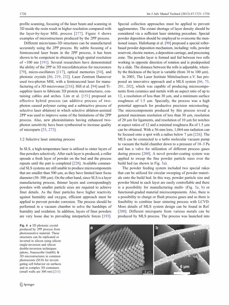
profile scanning, focusing of the laser beam and scanning in3D inside the resin result in higher resolution compared withthe layer-by-layer MSL process [277]. Figure 4 showsexamples of microstructures produced by the 2PP process.
Different micro/nano-3D structures can be manufacturedaccurately using the 2PP process. By subtle focusing of afemtosecond laser beam in the 2PP process, it has beenshown to be competent in obtaining a high spatial resolutionof ∼100 nm [191]. Several researchers have demonstratedthe ability of the 2PP in 3D microfabrication for microrotors[79], micro-oscillators [117], optical memories [54], andphotonic crystals [86, 219, 232]. Laser Zentrum Hannoverused two-photon MSL with a femtosecond laser for manu-facturing of a 3D microvenus [216]. Hill et al. [94] used Ti–sapphire lasers to fabricate 3D protein microstructures, con-taining cables and arches. Lim et al. [151] proposed aneffective hybrid process (an additive process of two-photon caused polymer curing and a subtractive process ofselective laser ablation) in which selective ablation-assisted2PP was used to improve some of the limitations of the 2PPprocess. Also, new photoinitiators having enhanced two-photon sensitivity have been synthesized to increase qualityof microparts [53, 273].
3.2 Selective laser sintering process
In SLS, a high-temperature laser is utilized to sinter layers offine powders selectively. After each layer is produced, a rollerspreads a fresh layer of powder on the bed and the processrepeats until the part is completed [228]. Available commer-cial SLS systems are still unable to produce microcomponentsthat are smaller than 500 μm, as they have limited laser focusdiameter (50–300 μm). On the other hand, since SLS is a layermanufacturing process, thinner layers and correspondinglypowders with smaller particle sizes are required to achievefiner details. As the finer particles have higher reactivityagainst humidity and oxygen, efficient approach must beapplied to prevent powder corrosion. The process should beperformed in a vacuum chamber to solve the hardships ofhumidity and oxidation. In addition, layers of finer powdersare very loose due to prevailing interparticle forces [193].
Special collection approaches must be applied to preventagglomerates. The extant shortage of layer density should beconsidered via a sufficient laser sintering procedure. Specialpowder deposition should be employed to overcome the men-tioned issues. Haferkamp et al. [90] proposed a special roller-based powder deposition mechanism, including: rolls, powderreservoir, electric motors, a deposition carriage, and processingzone. The powder layer is formed and fed between two rollsworking in opposite direction of rotation and is predepositedby a slide. The distance between the rolls is adjustable, where-by the thickness of the layer is variable (from 10 to 100 μm).
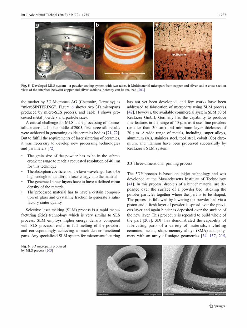
In 2003, The Laser Institute Mittelsachsen e.V. has pro-posed an innovative approach and a MLS system [66, 73,201, 202], which was capable of producing microcompo-nents from ceramics and metals with an aspect ratio of up to12, a resolution of less than 30 μm, and a minimum surfaceroughness of 1.5 μm. Specially, the process was a highpotential approach for productive precision microtooling.The microcomponents produced by this process reveal ageneral maximum resolution of less than 30 μm, resolutionof 20 μm for ligaments, and resolution of 10 μm for notchesat aspect ratios of 12 and a minimal roughness Ra of 1.5 μmcan be obtained. With a 56-mm lens, 1,064-nm radiation canbe focused onto a spot with a radius below 7 μm [226]. TheMLS can be connected to a turbo molecular vacuum pumpto vacuum the build chamber down to a pressure of 10–3 Paand has a valve for utilization of different process gasesduring process [200]. A novel powder-coating system wasapplied to sweep the fine powder particle sizes over thebuild bed (as shown in Fig. 5a).
The powder feeding system included two special rakesthat can be utilized for circular sweeping of powder materi-als onto the build bed. In this way, powder particle size andpowder blend in each layer are easily controllable and thereis a possibility for manufacturing multi- (Fig. 5a, b) orfunctional-graded material microcomponents. Also, there isa possibility to charge or flush process gases and so there isfeasibility to combine laser sintering process with LCVD.More details of MLS system design can be found in Ref.[200]. Different microparts from various metals can beproduced by MLS process. The process was launched into
Fig. 4 a 3D photonic crystalproduced by 2PP process fromphotosensitive material. Thesestructures can be replicated orinverted in silicon using siliconsingle-inversion and silicondouble-inversion techniques(photo, Nanoscribe GmbH). b3D microstructures in commonphotoresists (SU8) for investi-gating cell behavior on surfacesand in complex 3D containers(small walls are 300 nm) [211]
1726 Int J Adv Manuf Technol (2013) 67:1721–1754
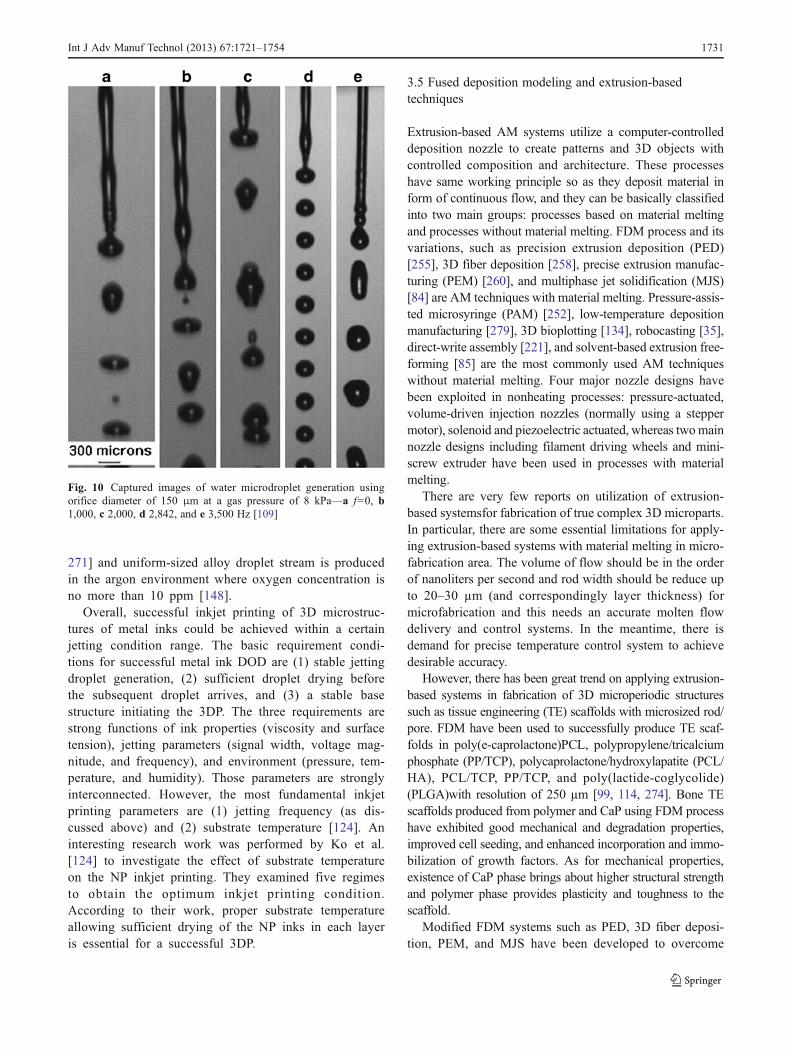
the market by 3D-Micromac AG (Chemnitz, Germany) as“microSINTERING”. Figure 6 shows two 3D micropartsproduced by micro-SLS process, and Table 1 shows pro-cessed metal powders and particle sizes.
A critical challenge for MLS is the processing of nonme-tallic materials. In the middle of 2005, first successful resultswere achieved in generating oxide ceramics bodies [71, 72].But to fulfill the requirements of laser sintering of ceramics,it was necessary to develop new processing technologiesand parameters [72]:
& The grain size of the powder has to be in the submi-crometer range to reach a requested resolution of 40 μmfor this technique
& The absorption coefficient of the laser wavelength has to behigh enough to transfer the laser energy into the material
& The generated sinter layers have to have a defined meandensity of the material
& The processed material has to have a certain composi-tion of glass and crystalline fraction to generate a satis-factory sinter quality
Selective laser melting (SLM) process is a rapid manu-facturing (RM) technology which is very similar to SLSprocess. SLM employs higher energy density comparedwith SLS process, results in full melting of the powdersand correspondingly achieving a much denser functionalparts. Any specialized SLM system for micromanufacturing
has not yet been developed, and few works have beenaddressed to fabrication of microparts using SLM process[42]. However, the available commercial system SLM 50 ofReaLizer GmbH, Germany has the capability to producefine features in the range of 40 μm, as it uses fine powders(smaller than 30 μm) and minimum layer thickness of20 μm. A wide range of metals, including: super alloys,aluminum (Al), stainless steel, tool steel, cobalt (Co) chro-mium, and titanium have been processed successfully byReaLizer’s SLM system.
3.3 Three-dimensional printing process
The 3DP process is based on inkjet technology and wasdeveloped at the Massachusetts Institute of Technology[41]. In this process, droplets of a binder material are de-posited over the surface of a powder bed, sticking thepowder particles together where the part is to be shaped.The process is followed by lowering the powder bed via apiston and a fresh layer of powder is spread over the previ-ous layer and again binder is deposited over the surface ofthe new layer. This procedure is repeated to build whole ofthe part [207]. 3DP has demonstrated the capability offabricating parts of a variety of materials, includingceramics, metals, shape-memory alloys (SMA) and poly-mers with an array of unique geometries [34, 157, 215,
Fig. 5 Developed MLS system—a powder coating system with two rakes, b Multimaterial micropart from copper and silver, and c cross-sectionview of the interface between copper and silver sections, porosity can be realized [203]
Fig. 6 3D microparts producedby MLS process [203]
Int J Adv Manuf Technol (2013) 67:1721–1754 1727

250]. 3DP allows the design and fabrication of complicatedscaffold shapes with a fully interconnected pore networkwith both a novel micro- and macroarchitecture [131].
In 3DP process, larger particles have lower surface pervolume and are simpler for spreading [156] and have largerpores results in fabrication of more homogeneous parts asbinders can immigrate better inward the powder bed [23].But like microsintering process, thinner layers and corre-spondingly powders with smaller sizes are required toachieve finer details (microscale features). Finer powdershave the potential profits of lower surface roughness, thin-ner layers, and promoted printability [206]. Also micro-3DPtechnology utilizes high-resolution piezoelectric printingheads instead of thermal printing heads (as used in normal-size 3DP) for building 3D microparts.
Digital Metal™ is a precision inkjet technology developedby Fcubic AB, Sweden for 3DP of micrometal componentswith a resolution of 20 μm and a surface finish of approxi-mately 4 μm (Ra). Digital metal technology offers uniquecapacity to rapidly produce highly complex and intricatedesigns and features for micron size metallic parts, cost-effectively in low-to-medium volumes. This process utilizes3DP and sintering process as a post-processing to producehigh-accuracy microcomponents. In this process, a specialsintering aid is spread as a binder over the powder in the areaswhich are part cross-section, in this way the area will fuse morequickly in a sintering furnace. By applying sintering aid as abinder, the part will sinter in at lower times and temperatures inthe furnace than encompassing powder that has not gottensintering aid. An important benefit of the micro-3DP processis that it is significantly a faster process compared with othermicro-additive processes and so it can be utilized for directmass production of microparts as well as microprototyping[111, 113]. In a collaborative workwith Fcubic AB, the authorshave evaluated the capability of Digital Metal 3DP process for3D thread fabrication. The result has been presented in Fig. 7.In this experimental work, the resolution of the process for thepart was 20 μm in x and y and 40 in z directions.
Also, 3DP process can be applied efficiently for directfabrication of microceramic molds. Charmeux et al. [36]investigated the manufacturability of microzirconia ceramicshells via 3DP for less expensive and a faster investmentcasting of microcomponents. Dimov et al. compared thecapabilities of the micro-3DP process to common two-stage investment casting to build metal microparts. Thiscomparative research work is concerned with the fabricationof sample microcomponents from stainless steel and Al/zinc
alloys with features in the range of 250 to 700 μm andaspect ratios up to 2.4. Corresponding to their report, micro-parts from Al and zinc alloys with features in 250 and500 μm and aspect ratio of 2.4 could be produce by 3Dprinted ceramic micromolds with accuracy around 5 and20 % of the nominal dimension, respectively.
3.4 Inkjet printing processes
Inkjet printing processes are based on inkjet technology andinclude arrangement and layer-by-layer deposition of a liquidmaterial in droplet form. Droplets of liquid materials usuallycalled fluid or ink. The material often turns into solid subse-quent to the deposition process via cooling (e.g., by crystalli-zation or vitrification), chemical changes (e.g., through thecross-linking of a polymer), or solvent evaporation. Also, otherpost-processing procedures like sintering could be included.
In inkjet printing technology, two different techniquesprevalently are utilized for droplet creation, namely, drop-on-demand (DOD) and continuous inkjet (CIJ). Generally,CIJ systems operate with fluids of lower viscosity than DODand at a higher drop velocity [96] and so DOD technique hasmore potential for 3D microfabrication. In DOD technique,ink droplets are solely delivered when they are demanded tobe printed. Thus, there is no necessity for unused liquidrecycling. The droplets of desirable material are ejected froman ink vat in reaction to an activate signal, through pressurepulse which is generated by an actuator. There are two mainkinds of actuator: thermal and piezoelectric actuators. In ther-mal DOD, a transitory bubble of vapor is created by fast andglancing heating of the ink using a small electrical heatingelement situated in the ink reservoir close to the print headnozzle. Creation of this bubble of vapor results in injection ofa jet of ink from the nozzle. The thermal DOD technique (alsocalled bubble jet) is broadly utilized in typical office printers.The piezoelectric element is the more common industrialsystem which makes a change in the internal volume of theink reservoir using an electric field to create pressure waves.The pressure waves results in ink ejection from the print headnozzle and afterward correspondingly filling again the reser-voir [96]. Vaporization of small volume of the ink results inconsequential limitations on the usable materials in the ther-mal DOD process. The materials must be comparatively vol-atile (or have a component which is volatile), while, thepiezoelectric DOD method has no such limitation. For bothmentioned methods of DOD, print heads usually includeseveral separate nozzles which are fed via a single-ink mani-fold in a participatory manner but each separately controllable.
Turning of the fine droplets into solid (phase transition) canalso be accomplished by curing of a photopolymer ink usingUV light in inkjet printing process. Two inkjet printing sys-tems, including: Eden printer by Objet Geometries and ProJetprinter by 3D Systems have been commercialized based on
Table 1 Processed metal powders and their grain sizes [73]
Materials Copper Tungsten Silver Aluminum
Particle size 10 μm 300 nm 2 μm 3 μm
1728 Int J Adv Manuf Technol (2013) 67:1721–1754

the same principle. Objet’s printers use special print headswith many individual nozzles to deposit a number of differentacrylic-based photopolymer materials with 42-μm resolutionand in 16-μm layers. Each photopolymer layer is cured by UVlight immediately as it is printed, producing fully cured mod-els. Support structures are built in a gel-like material, which isremoved by hand and water jetting [82]. ProJet printer uses thesame technique barring that support structure used with thismachine is a wax which has a much lower melting tempera-ture than the part printed and is easily melted out. This methodof “hands-free” support removal allows for highly complex3D micocomponents/assemblies and delicate applications.Figure 8 shows sample microparts with 400-μm blade thick-nesses which have been fabricated via different commerciallyavailable inkjet-based systems, including Eden 260 V, ProJetHD 3000plus, as well as Solidscape’s T76 3D printer which isa commercial piezoelectric DOD micro-AM system for print-ing of polymer inks.
As seen in Fig. 8, the blade produced via ProJet 3000 HDhas better dimensional stability and surface quality than Eden3D printer due to higher resolution (34 μm) and hands-freesupport removal. Support material between some blades can beseen in ProJet’s micropart, although it has a smoother surfacethan Eden printer. Better finishing may solve this problem. Theedges of the blades are sharper in Solidscape’s micropart, andthey have better surface quality as compared with ProJet andEden printers. Nevertheless, some extra material (not supportmaterial) can still be seen between blades in Solidscape’s
micropart. It is believed that the most important limitation ofinkjet printing systems is currently support removal for com-plex 3D microstructures. In the meantime, resolution of theprocess should be improved to expand the range ofapplications.
Other specialized piezoelectric DOD microfabrication sys-tems have been developed by MicroFab technologies, USAfor high-quality micropart fabrication. MicroFab’s DOD tech-nology has been used by many researchers to investigateeffective parameters on microdroplet generation. Figure 9shows typical experimental set up used by Ko et al. [124] inwhich build plate can move in x and y directions and metalnanoparticles (NP) droplets are observed by a CCD camera.
In such DOD experimental system, droplets are ejectedthrough voltage waveform changes (Fig. 9 inset graph). Inshort, the first rising voltage expands the glass capillary and adroplet is pushed outside the nozzle due to the falling voltage.The final rising voltage cancels some of the residual acousticoscillations that remain after drop ejection and may causesatellite droplets. The signal generator used to produce micro-droplets also triggers the CCD camera, so that the CCDcaptures images at the droplet generation frequency [124].
Viscosity, inertia, and surface tension are three mainfactors which affect the behavior of drops and liquid jets.Some dimensionless parameters such as Reynolds number(Re), Weber number (We), and Ohnesorge number (Oh) areused for describing and analyzing jetting and break-up phe-nomena in microdroplet generation. The Re is a
Fig. 7 3D microthreadsfabricated in a collaborativeresearch work using Fcubicprocess, outside M5 thread andtwo M2 inside threads
Fig. 8 Sample microparts with 400 μm blade thickness produced usingdifferent inkjet printing systems—a Solidscape’s T76, the part was madewith ∼5-μm resolution and in 12.7-μm layers; b 3D System’s ProJet HD
3000plus, the part was made in the extreme high-definition modus (34-μm resolution and 16-μm layers); and c Objet’s Eden 260 V 3D printer,the part was made with (42-μm resolution and in 16-μm layers)
Int J Adv Manuf Technol (2013) 67:1721–1754 1729

characteristic which describes the ratio between inertial andviscous forces and obtained by Re0ρdv/η, where v is fluidvelocity, η is dynamic viscosity, d is specific length (dropletdiameter), and ρ is fluid density. The We is a characteristicwhich describes the ratio between kinetic energy and surfaceenergy: i.e., between inertial and surface forces and obtainedby We0ρdv2/б, where б is surface tension. Also, the Oh is acharacteristic which describes the relative importance ofviscous and surface forces and obtained by Oh0We1/2/Re0η/(ρбd)1/2 [96]. According to research works of Wanget al. [255] and Derby and Reis [56], for Oh>1, fluid viscousdissipation results in orifice clogging and impedes ejectionof drops and also for Oh<0.1 multiple drops is produceinstead of a single well-defined drop. So, in practice, jett-ability criterion for precision DOD printing is 1>Oh>0.1and correspondingly droplet velocity should be 5–10 m/s.Table 2 shows jettability criterion for both CIJ and DODprocesses. It should be noted that for non-Newtonian fluids,other parameters such as the Weissenberg number (Wi) isused to blend the effects of viscoelasticity. The Wi value canbe obtained by Wi0Tv/d, where T is a characteristic relaxa-tion time of droplet [96, 150].
Disturbance frequency has important effect on formationsof jet and break-up [148]. The optimum disturbance frequency(fopt ) can be estimated in the following equations [109]:
fopt ¼ vj
pdjffiffiffiffiffiffiffiffiffiffiffiffiffiffiffiffiffiffiffiffiffiffiffiffiffiffi
2 1þ 3ZOhð Þp ð1Þ
vj ¼ k � v0 ð2Þ
v0 ¼ 2
3
ffiffiffiffiffiffiffiffiffiffiffiffiffiffiffiffiffiffiffiffiffiffiffiffiffiffiffiffiffiffiffiffiffi
3ΔP
pjþ 1; 024μ2
j
d20p2j
s
� 64μj
3d0pjð3Þ
Where dj is jet diameter, ΔP is gas pressure in the inkreservoir, d0 is orifice diameter, ρj is ink density, μj is jetviscosity and is jet velocity which has direct relation withorifice velocity v0. The orifice velocity as well as the jetvelocity increases with the gas pressure in the ink reservoir.
Coefficient k should be calibrated for the different nozzlesand the materials [109]. The influences of the disturbancefrequency on the droplet generation for two different fluids,namely, water and Sn63/Pb37 metallic ink were investigatedby Jiang et al. [109]. As an example, Fig. 10 shows theimages of water droplet generation which were captured bythe high-speed CCD camera.
As seen in Fig. 10b, c, e, the droplets merge with eachother to form bigger droplets due to the difference of thedroplet velocities. According to this visual experiment, thesatellite droplets and the merged droplets cause degradationof the droplet diameter accuracy. As seen in Fig. 10d, whenthe imposed disturbance frequency is selected properly, thedroplets are round with uniform sized and spaced with thesame distance [109].
Inkjet printing is used for microprinting of both me-tallic and nonmetallic (usually polymers) materials butDOD printing of metal inks needs special configurationsto control jetting process for achieving well-defineddroplets. For example, jetting process should be per-formed in a low-oxygen environment to avoid the oxi-dation of the jet and the microdroplets. Researches havedemonstrated that the molten metal in high oxygenenvironment reacts with oxygen to form a surface oxidelayer which changes the physical properties of the jetsurface and prevents the jet from disintegrating [130,
Fig. 9 Typical piezoelectricDOD printing system [124]
Table 2 Comparison of droplet parameters for standard commercialcontinuous inkjet (CIJ) and drop-on-demand (DOD) printers (takenfrom [96])
Parameters DOD CIJ
Fluid viscosity (mPas) 10–100 2–10
Droplet diameter (μm) 10–150 10–150
Droplet volume (pL) 0.5–2,000 0.5–2,000
Droplet velocity (m/s) 5–10 10–20
Reynolds No. 2–50 100–1,000
Weber No. 50–150 500–1,500
Ohnesorge No. 0.1–1 0.03–0.2
1730 Int J Adv Manuf Technol (2013) 67:1721–1754
271] and uniform-sized alloy droplet stream is producedin the argon environment where oxygen concentration isno more than 10 ppm [148].
Overall, successful inkjet printing of 3D microstruc-tures of metal inks could be achieved within a certainjetting condition range. The basic requirement condi-tions for successful metal ink DOD are (1) stable jettingdroplet generation, (2) sufficient droplet drying beforethe subsequent droplet arrives, and (3) a stable basestructure initiating the 3DP. The three requirements arestrong functions of ink properties (viscosity and surfacetension), jetting parameters (signal width, voltage mag-nitude, and frequency), and environment (pressure, tem-perature, and humidity). Those parameters are stronglyinterconnected. However, the most fundamental inkjetprinting parameters are (1) jetting frequency (as dis-cussed above) and (2) substrate temperature [124]. Aninteresting research work was performed by Ko et al.[124] to investigate the effect of substrate temperatureon the NP inkjet printing. They examined five regimesto obtain the optimum inkjet printing condition.According to their work, proper substrate temperatureallowing sufficient drying of the NP inks in each layeris essential for a successful 3DP.
3.5 Fused deposition modeling and extrusion-basedtechniques
Extrusion-based AM systems utilize a computer-controlleddeposition nozzle to create patterns and 3D objects withcontrolled composition and architecture. These processeshave same working principle so as they deposit material inform of continuous flow, and they can be basically classifiedinto two main groups: processes based on material meltingand processes without material melting. FDM process and itsvariations, such as precision extrusion deposition (PED)[255], 3D fiber deposition [258], precise extrusion manufac-turing (PEM) [260], and multiphase jet solidification (MJS)[84] are AM techniques with material melting. Pressure-assis-ted microsyringe (PAM) [252], low-temperature depositionmanufacturing [279], 3D bioplotting [134], robocasting [35],direct-write assembly [221], and solvent-based extrusion free-forming [85] are the most commonly used AM techniqueswithout material melting. Four major nozzle designs havebeen exploited in nonheating processes: pressure-actuated,volume-driven injection nozzles (normally using a steppermotor), solenoid and piezoelectric actuated, whereas twomainnozzle designs including filament driving wheels and mini-screw extruder have been used in processes with materialmelting.
There are very few reports on utilization of extrusion-based systemsfor fabrication of true complex 3D microparts.In particular, there are some essential limitations for apply-ing extrusion-based systems with material melting in micro-fabrication area. The volume of flow should be in the orderof nanoliters per second and rod width should be reduce upto 20–30 µm (and correspondingly layer thickness) formicrofabrication and this needs an accurate molten flowdelivery and control systems. In the meantime, there isdemand for precise temperature control system to achievedesirable accuracy.
However, there has been great trend on applying extrusion-based systems in fabrication of 3D microperiodic structuressuch as tissue engineering (TE) scaffolds with microsized rod/pore. FDM have been used to successfully produce TE scaf-folds in poly(e-caprolactone)PCL, polypropylene/tricalciumphosphate (PP/TCP), polycaprolactone/hydroxylapatite (PCL/HA), PCL/TCP, PP/TCP, and poly(lactide-coglycolide)(PLGA)with resolution of 250 µm [99, 114, 274]. Bone TEscaffolds produced from polymer and CaP using FDM processhave exhibited good mechanical and degradation properties,improved cell seeding, and enhanced incorporation and immo-bilization of growth factors. As for mechanical properties,existence of CaP phase brings about higher structural strengthand polymer phase provides plasticity and toughness to thescaffold.
Modified FDM systems such as PED, 3D fiber deposi-tion, PEM, and MJS have been developed to overcome
Fig. 10 Captured images of water microdroplet generation usingorifice diameter of 150 μm at a gas pressure of 8 kPa—a f00, b1,000, c 2,000, d 2,842, and e 3,500 Hz [109]
Int J Adv Manuf Technol (2013) 67:1721–1754 1731
FDM limitations in terms of feedstock shape and resolution.New configurations for melt extrusion could open up thepossibility for the use of a wider range of biomaterials,making the extrusion-based systems more versatile and re-alizable alternative manufacturing process for compositescaffold materials. Nevertheless, there was still limitationin terms of the high heat effect on raw biomaterial andresolution of the process. Thus, researchers made attemptsto develop new configurations without material melting thatcan better preserve bioactivities of scaffold materials. PAMprocess is a technique developed by Vozzi et al. [252] thatresembles FDM process without the need for heating. PAMuses a pneumatic driven microsyringe to deposit biomaterialon a substrate with resolution of 10 µm. Polymeric scaffoldswith different polymers compositions such as PCL, poly(L-lactic acid) (PLLA), PLGA, PCL/PLLA, gelatin, and algi-nate hydrogels scaffolds with three different geometries-square grids, hexagonal grids, and octagonal grids wereproduced [168, 241, 242, 251, 253]. Vozzi’s group used amodified system called piston-assisted microsyringe formicrofabrication of viscous, sol–gel, or gelled inks (e.g.,alginate solutions at different concentrations) [243].
3D bioplotting is a technique that was first developed byLanders and Mulhaupt [134] at Freiburger group to produce3D scaffolds with micron sized rods for soft tissue engineer-ing purposes, and simplifying hydrogel manufacturing. Inthis process, the material dispensing head normally movesin three dimensions, while the fabrication platform is sta-tionary. Either a filtered air pressure (pneumatic nozzle) or astepper motor (volume-driven injection nozzle) is used toplot a viscous material into a liquid (aqueous) plottingmedium with a matching density. It is possible to performeither a discontinuous dispensing of micro dots or a contin-uous dispensing of fine filaments. In comparison to otherextrusion-based SFF processes, 3D Bioplotting can processa remarkably wide variety of different biomaterials, includ-ing polymer melts, thermoset resins, polymer solutions, andpastes with high filler contents, bioactive polymers such asproteins. The plotting of biomaterials such as melts of PLA,PLGA, poly-(hydroxybutyrate-co-valeriate) biodegradablethermoplastic, PCL, and poly(butylene terephthalate-block-oligoethylene oxide), biopolymer solutions of agar and gel-atin [133], natural polymers, such as collagen, and reactivebiosystems involving fibrin formation and polyelectrolytecomplexation is possible. 3D bioplotting can process ther-mally sensitive biocomponents, and cells since heating isnot applied.
Khalil et al. [118] developed a special multinozzle bio-plotter which was capable of extruding biopolymer solu-tions and living cells for freeform construction of 3D tissuescaffolds. The deposition is not occurred into plotting mediabut is biocompatible and occurs at room temperature andlow pressures to reduce damage to cells. Ang et al. [5] set up
a special robotic bioplotting device called rapid prototypingrobot dispensing (RPBOD) for the design and fabrication ofchitosan-HA scaffolds. Furthermore, the RPBOD systemwas improved to include a new manufacture method, calleddual dispensing system as besides the pneumatic dispenser,a mechanical dispenser which was driven by a stepper motorwas set up to deposit plotting medium [133].
Variety of extrusion-based AM techniques has also beendeveloped for processing of ceramics. Robocasting is atechnique in which a computer controls the deposition ofhighly concentrated (typically 50–65 vol% ceramic powder)colloidal ceramic slurries. Solvent-based extrusion free-forming is a ceramic processing technique developed byour research group to produce bioceramic scaffolds[266–268, 270] and electromagnetic band gap materials[11]. In this process, continuous flow of materials in formof paste or particulate slurries is dispensed on to the surfaceusing a 3D motion system incorporated with the nozzle.Solvent-based extrusion freeforming is relatively simpleprocess in which phase change is based on solvent evapo-ration. Paste with high yield strength is prepared by blend-ing polymer, ceramic, and a solvent with specific ratios.Defects such as dilatancy, drying cracks and surface fracturewhich happens in water-based extrusion systems can beeliminated by appropriate adjustment of polymer content[269].
Direct-write assembly is an extrusion-based system de-veloped by Lewis et al. [221] whereby a wide range of inkscan be patterned in both planar and 3D shapes with featuresizes as fine as 250 nm. In this process, compressed air isemployed to push inks with controlled rheological proper-ties through an individual nozzle (diameter ranging from 1to 500 µm). Direct-write assembly deposits inks at roomtemperature or a proper coagulation reservoir using a con-trolled-printing speed and pressure which depend on inkrheology and nozzle diameter. A wide range of inks includ-ing colloidal suspensions and gels, nanoparticle-filled inks,polymer melts, fugitive organic inks, hydrogels, sol–gel,and polyelectrolyte inks have been processed using direct-write assembly. Lewis et al. have reached to minimumfeature sizes ranging from 250 nm for sol–gel inks and200 µm for ceramic colloidal inks. Writing of some inkssuch as polyelectrolyte inks need to be performed into areservoir-induced coagulation to enable 3D printing, where-as some other inks such as sol–gel inks can be directlyprinted in air providing excellent control over the depositionprocess (e.g., the ink flow can be started/stopped repeatedlyduring assembly).
Figure 11 depicts TE scaffolds with different rod widths,pore size, and materials have been made by the authorsusing two processes with and without material melting,namely, FDM and solvent-based extrusion freeformingtechniques.
1732 Int J Adv Manuf Technol (2013) 67:1721–1754

3.6 Laminated object manufacturing process
LOM system uses laser beam to cut out expected profilesfrom sheet, provided from an uninterrupted roll, whichcreate final-part layers. Layers stick together by applying aheat-activated plastic which is plated on one surface of thepaper and final part [123].This additive process has severallimitations (mainly resolution) for micropart fabrication andis not a potential method to be used in a true 3D micro-fabrication area. This method is currently used for fabrica-tion of ceramic structures with microscale internal cavitiesand channels favorable for microfluidic devices. Computer-Aided Manufacturing of Laminated Engineering Materials(CAM-LEM, Inc., USA) has developed special micro-LOMprocess known as CAM-LEM process. In CAM-LEM pro-cess, slices are produced by laser cutting metal tape or sheetof green ceramic. Next, the slices are stacked accurately tocreate the part. Afterward, the layers are bonded together byapplying heat and pressure. The green part is then put intofurnace to obtain sufficient strength. Five kinds of materialswith different thicknesses can be automatically utilized intoa build process. One or more of the materials may work assupport materials. Support materials enable the process tobuild overhangs and internal microvoids/microchannels.The support materials are taken away by using thermal/chemical methods. The main drawback of the process is alarge amount of shrinkage (12–18 %) due to thermal post-processing which can lead to dimensional inaccuracies [82].Layer thickness can range from 30 to 1,300 μm or more,although most common materials are between 150 and600 μm. CAM-LEM process enables the creation of high-performance microfluidic devices made from ceramic ormetal. These provide much better chemical resistance andstrength than plastic or silicon, better strength than glass,and high-temperature resistance. CAM-LEM process can beused for fabrication of microsensors, miniature diagnosticdevices, lab-on-a-chip, microreactors and heat exchangers,and microfuel cell components.
4 Key 3DDW processes
LCVD, FIBDW, and nozzle dispensing systems are the key3DDW techniques. Nozzle dispensing systems such as direct-write assembly, PAM, etc were discussed earlier in section 3.5along with FDM process. In the following section two DWprocesses, namely, LCVD and FIBDW would be described.
4.1 Laser chemical vapor deposition process
LCVD is a 3DDW process that employs laser beam toconvert gaseous reactants into thin solid layers in a selectivemanner. In LCVD process, laser beam is focused to a spot(∼1 μm in diameter) via optical microscope lens and gas-eous reactant comprising the materials to be laid down is fedinto a build chamber. The substrate is heated selectively byscanning the laser beam over it at usually 0.5–5 mm/s speedto dissociate the reactant gas selectively; consequently, athin layer of the material is set down onto the substrate. Inthis way, by repeating laser scan, expected microcomponentcan be made layer by layer. There is a possibility to fabricatemultimaterial and gradient 3D microstructures by feedingdifferent gases into the build chamber at different times orusing a blend of gases with desirable concentrations.Researchers at the Georgia Institute of Technology devel-oped a LCVD system which uses jets of gas to provide alocal gaseous atmosphere instead of feeding gaseous pre-cursor materials into the build chamber [82].
Various microparts from variety of ceramics and metalscan be produced by LCVD process using different reactantgases. Furthermore, LCVD process can be used to buildcarbon fibers and multilayered carbon structures. Duty etal. [64] deposited various materials including carbon, siliconcarbide, boron, boron nitride, and molybdenum (Mo) ontovarious substrates including graphite, grafoil, zirconia, alu-mina, tungsten, and silicon using the Georgia Tech’s LCVDsystem. In 1994, 3D aluminum oxide (Al2O3) rods of 3–20 μm diameters were fabricated by Lehmann and Stuke
Fig. 11 a Plane view of HA scaffold with rod width of 70 µmproduced by solvent-based extrusion freeforming. Bioceramic scaf-folds produced by solvent-based extrusion freeforming have the finestrod width among other extrusion-based SFF techniques such as direct-
write assembly orrobocasting. b PLA scaffold with micropores fabri-cated using screw-feed FDM system, rod width of 250 µm and air gapsare 100 µm
Int J Adv Manuf Technol (2013) 67:1721–1754 1733

using LCVD process with growth rate of up to 80 μm/s.They used a special blend of trimethylamine alane ((CH3)3N.AlH3) and oxygen as gas precursor and two orthogonalargon laser beams with 0.2–20 mW power and spot diameterof 3 μm was used instead of a single laser beam [147].Wanke et al. [256] employed the process with growth rateup to 100 μm/s to fabricate 3D photonic microparts fromAl2O3 and the technique was later employed by Stuke et al.[227], for fabrication of 3D microelectrical cages to snaremicroparticles. William et al. [257] utilized LCVD processto fabricate carbon 3D microcoils using ethylene gas pre-cursor. Figure 12 shows a sample Al2O3 3D microstructureproduced by LCVD process.
A number of factors such as laser beam diameter, energydensity, and wavelength as well as substrate thermal prop-erties influence the resolution of this process [82]. Also, thedeposition rate is contingent upon the process parameterssuch as scanning speed, gas pressure, and laser power den-sity. Increasing in gas pressure of the precursor materialsand laser power density results in linearly increase of depo-sition rate. Also, scanning speed is inversely proportional tothe deposition rate [257] and the grain size increases withdeposition thickness, as reported by Foulon and Stuke [77].Deposition thickness can be estimated by the equation of-fered by William et al. [257], for a Gaussian beam profile:
h vs; tð Þ ¼ R0rtffiffiffi
pp
ffiffiffi
pp
r þ 2 vstð ÞIn this equation, r is the laser spot radius, hðvs; tÞ is the
deposition layer thickness, R0 is the diffusion-limited axialgrowth rate, vs is the scanning speed, and t is process time.
4.2 Focused ion beam direct writing
The principle of FIBDW is similar to LCVD process barringthat FIB is employed instead of laser beam for deposition. Inthis process, a FIB generated from a liquid gallium source isscanned over a build substrate in the presence of gaseousprecursors and as a result solid materials are deposited onto
the substrate [95, 155]. As compared with LCVD, FIBDWhas lower deposition rate (normally, 0.05 μm3/s) but alsooffers higher resolution. Energy of the ion beam is usuallybetween 10 and 50 keV, with beam currents changing be-tween 1 pA and 10 nA. The minimum deposition thicknessis about 10 nm for microstructures with the minimum fea-ture size of 80 nm and aspect ratios between 5 and 10 [185].Since organometallic mixtures are utilized in FIBDW, metallayers deposited are not pure due to Ga+ ions and organicimpurity [67]. Reyntjens and Puers utilized W(CO)6 as anorganometallic precursor gas for deposition of W [205].Different microstructures have been fabricated from con-ductors, such as gold (Au), Al, copper (Cu), Mo, and Ptand insulators, such as TEOS, TMCTS/O2, and PMCPS/O2
using different gases [29, 68, 272]. FIBDW is a slow pro-cess, so it is usually employed for repair work and low-volume production [184]. In particular, this process can beused for fabrication of 3D microstructures which are utilizedfor hermetic encapsulation in microsensors [96]. It shouldbe noted that electron beam can also be utilized to induceCVD in a similar way to FIBDW and LCVD. Both electronbeam CVD and FIBDW have a better resolution thanLCVD, but electron beam CVD is a slower process ascompared with LCVD and FIBDW [21].
5 Key hybrid process
Two processes namely, EFAB and SDM are subset to thisgroup. Only EFAB process has been discussed in this sec-tion since to date SDM has not shown applicability for true3D micromanufacturing.
5.1 Electrochemical fabrication process
The EFAB is a hybrid process for volume manufacturing ofmicrodevices with features as small as 20 μm and tolerancesof ±2 μm with no assembly. EFAB process is a trademark ofMicrofabrica (formerly MEMGen Corp.) and is based onmultilayer electrodeposition and planarization of at least twometals: one structural material and one sacrificial material[48]. Figure 13 shows the EFAB process schematically.
The EFAB is a hybrid (additive/subtractive) process inwhich three-step process is used to generate each layer. Thisthree-step process is repeated to build the desired complexmicrodevices layer by layer. The three-step process in eachlayer includes: structural material electrodeposition, sacrifi-cial material electrodeposition, and planarization, respec-tively. Both materials are deposited by electroplating, andone (sacrificial material in Fig. 13) is deposited using aspecial selective electroplating process called “instant mask-ing.” The EFAB process begins by electrodeposition ofsacrificial material using instant masking. Using instant
Fig. 12 Aluminum oxide 3D microstructure produced via LCVDprocess (photo, MPI-Göttingen, Germany, taken from [81])
1734 Int J Adv Manuf Technol (2013) 67:1721–1754

masking, a negative micromold is generated by customphotolithography process in which a precise thickness ofphotoresist is exposed to the UV light selectively throughphotomask to generate a pattern. The produced micromoldis placed into an electrodeposition to deposit sacrificialmaterial (Cu). The photoresist is then chemically removedand the structural material is deposited into the area wherethe photoresist was removed. The structural material fills inthe gaps between parts on each layer. Then, both the sacri-ficial and structural materials are planarized to the samelevel, establishing the desired layer thickness (2–25 μm).All sacrificial material is etched from the wafer and removedfrom the devices. There is a possibility to achieve micro-features up to 20 μm with 2 μm accuracy and repeatabilityby the EFAB process. Limited materials have been devel-oped by Microfabrica, including: Valloy-120, a nickel–co-balt (Ni–Co) alloy that has mechanical properties that aresimilar to medical-grade stainless steel; Edura-180, an elec-troplated rhodium (platinum (Pt) group metal) formulationthat is almost as hard as ceramic and has high electricalconductivity; and biocompatible noble metal palladium.Valloy-120 is used as the primary structural material and isan electroplated, fully dense, ductile, corrosion-resistantmetal with great mechanical properties and biocompatibilityfor short time exposure to tissue. Edura-180 is usually usedwhere extreme hardness or wear resistance is required inthin walls. Noble palladium is also served where excellentbiocompatibility is required. Properties of commerciallyavailable EFAB materials compared with some commonlyused medical materials can be found in Cohen et al. [46].The EFAB process is an ideal approach for producing robust
micrometal parts, subassemblies, and 3D micromachines.This process has a wide range of applications in micro-industries, including probes for semiconductor testing,microfluidic devices, minimally invasive medical instru-ments and implants, high accuracy probes for testing mem-ory chips and microprocessors, inertial sensing devices,military fuzing, and millimeter wave components [46].Figure 14 shows two 3D microstructures/assemblies pro-duced by the EFAB process.
6 Impacts, applications, and future trends
6.1 Impacts of 3D micro-AM technologies
MEMS processes are silicon-based manufacturing processes(including bulk and surface micromachining), soft lithogra-phy, and LIGA process. In silicon bulk micromachiningprocesses, a silicon wafer (or other crystalline materials) isetched, typically anisotropically, to form structures. In sili-con surface micromachining processes, layers of polycrys-talline silicon are deposited to form structures, typically withoxides deposited as a sacrificial material. Finally, in theLIGA process, a thick polymer layer is exposed to hard X-ray radiation from a synchrotron to define apertures inwhich are then deposited a metal such as Ni or Cu. To date,silicon micromachining approaches have had great effect ongrowth and development of microproducts such as sensorsbut they still have some considerable drawbacks that areobstacles for emersion of new microproducts and havelimited silicon micromachining applicability to some
Fig. 13 The EFAB process [27]
Int J Adv Manuf Technol (2013) 67:1721–1754 1735

commonly used components such as diaphragms, cantileverbeams, etc. Moreover, silicon micromachining is an expen-sive, inflexible, high-risk, and time consuming approachwhere new microproducts need to be developed. 3Dmicro-AM technologies provide many benefits as comparedwith conventional silicon micromachining technologies.The most significant advantage of 3D micro-AM technolo-gies is the aptitude to fabricate true 3D components/struc-tures. Prior to micro-AM technologies, designers have beencompelled to take into consideration the limitations of sili-con micromachining that is intrinsically planar when design-ing MEMS/MOEMS devices. In many cases, this limitationis an obstacle to achieve optimum performance of micro-products. Hence, adding 3D capability to design can openup new application areas and solves problems that havehindered MEMS/MOEMS industry. Table 3 shows someexamples in which 3D micro-AM processes can be appliedto fulfill performance requirements that would be unobtain-able using conventional planar techniques.
Using 3D micro-AM processes, microstructures can befabricated thin where flexibility is required and thick whererigidity is required. Unwanted vibration modes can be elim-inated, proof masses can be increased in size, electrodes andshielding can be placed in optimal locations, and systemscan be designed with more degrees of freedom and greaterfunctionality [43]. Also, micro-AM processes makes possi-ble an unprecedented level of device complexity, includingthe creation of fully assembled mechanisms with multipleindependent, moving parts which can avoid the need forcostly microassembly [49].
As a consequence of what was discussed above, 3D micro-AM processes enables new types of designs previously im-possible to produce while offering cost reduction on specifictypes of microdevices. Silicon technology has still a justifica-tion for its existence and is still a preferable approach in manycases in terms of cost, time, functionality, and reliability.Silicon technology has shown its success in many differentapplications, and currently micro-AM technologies can be aneffective tool when there is complexity. In fact, choosing
silicon technology or micro-AM technology would be a de-batable issue only if microproducts have complexity. It isbelieved that micro-AM technologies need more improvementin terms of cost and reliability to broaden their fields ofapplications. Popularity of silicon inMEMS/MOEMS ismain-ly due to its mechanical properties. Silicon is a semiconductorwhich has mechanical properties similar to ceramics such ascorrosion resistance, high strength, and no plastic yielding orfatigue behavior at moderate temperatures. In particular, singlecrystal silicon is an ideal choice for resonant microsystems thatneed high-Q resonant characteristic and very long cycle life.Therefore, micro-AM technology should be able to live up tomaterial-related reliability expectation to become a standardtool in the micromanufacturing area in the future.
Choosing the right 3D micro-AM process to be used needsa comprehensive knowledge on capabilities and limitations ofeach process. A comparison of 3D micro-AM systems hasbeen presented in Table 4. Figure 15 graphically compares 3Dmicro-AM processes and various conventional micromanu-facturing methods as well as some important MEMS manu-facturing processes in terms of complexity and feature size.
As seen in Fig. 15, conventional fabrication technologiessuch as bulk micromachining and polysilicon surface micro-machining are still preferable approaches for structures withrather low intricacy. But for components with high com-plexity, micro-AM processes are more favorable. It shouldbe noted that for microproducts with very high intricacyEFAB is the best solution among micro-AM processes thatcan fulfill device assembly.
Silicon is not the ideal material for every applicationsince it is very brittle and tends to fail unexpectedly andcalamitously at high loads (e.g., shock and vibration). Forthis reason, protecting silicon from surrounding environ-ment is one of the most significant challenges in siliconmicroproduct packaging. Thus, utilization of 3D micro-AM processes for fabrication of microproducts from differ-ent robust materials which have less severe packagingrequirements can be an efficient measure to solve packagingproblems. Most of micro-AM systems are able to produce
Fig. 14 a Hybrid couplers and RF switches for millimeter-wavesystems [38]. b Different microstructures, including: a fluid injectorarchitecture, fluidic wells and channels, an array of helical inductors,
electrical resistance structures, an accelerometer with capacitive senseplate, geometries for plastic micromolding and embossing, producedfrom electroplated nickel in 24 layers using EFAB process [43]
1736 Int J Adv Manuf Technol (2013) 67:1721–1754

Table 3 MEMS component design using 3D micro-AM processes and conventional planar micromanufacturing techniques (reproduced from [43])
Design examples Description
MEMS switch: a) Design for manufacturing with conventional planar micromanufacturing approaches b) Design for manufacturing with 3D micro AMprocesses
In the conventional approach (a), a cantilever beamis suspended above the substrate, and is driven byelectrodes on the substrate to contact another electrode on the substrate to close a circuit. There isa fundamental trade-off between the drive voltage and isolation of a MEMS switch. That is, increasingthe gap between the suspended beam and the substrate improves isolation at the cost of increased drive voltage. However, this trade-off is based onthe assumption that electrodes must lie flat on the substrate (a planar assumption). With 3D micro AM technologies, there are more optimal ways toplace drive electrodes, for example by coupling the beam separately to a set of stacked electrodes (b).The design using 3D micro AM processes providesimproved isolation, reduced drive voltage, and double-throw functionality.Capacitive pressure sensor: a) Design for manufacturing with conventional planar micromanufacturing approaches b) Design for manufacturing with 3D micro AMprocesses
A silicon capacitive pressure sensor (a) is typically comprised of two micromachined and bondedsilicon wafers. The die must be protected in anexternal package. With 3D micro AM technologies(b), it is possible to fabricate a metal diaphragm pressure sensor which provides a substantiallylarger sense capacitance using stacked electrodes, as well as self-packaging and improved media compatibility.
Gap Closing Actuator:a) Design for manufacturing with conventionalplanar micromanufacturing approaches b) Design for manufacturing with 3D micro AMprocesses
Larger forces for gap closing actuators can berealized by increasing the actuator height using 3Dmicro AM processes since there is no limitation inheight of microparts.
Gap Closing Actuator:a) Design for manufacturing with conventional planar micromanufacturing approaches b) Design for manufacturing with 3D micro AMprocesses
Larger forces for gap closing actuators can berealized by increasing the number of actuatorlayers.
Int J Adv Manuf Technol (2013) 67:1721–1754 1737

microparts from a variety of metals which have many usefulproperties such as high electrical and thermal conductivity,greater fracture resistance than silicon, high reflectance,high temperature stability, and magnetic properties.Fatigue is the most significant disadvantage of metals forMEMS/MOEMS devices as compared with silicon.Nevertheless, several high-cycle resonant devices have been
produced from metals instead of silicon such as TexasInstruments’ DMD which is used in projection MSLsystems as discussed in Section 3.1. It is believed thatfatigue effect can be controlled in microsystems pro-duced from metals if microproduct is designed appro-priately for remaining cyclic operating stresses withinelastic boundaries.
Table 4 Comparison of the key micro-AM systems
Process Strengths and weaknesses Resolution(μm)
Materials References
MSL Complicated, yet well-understood and proventechnology, high-resolution, suitable forvolume production, suitable for true 3Dmicroparts, high repeatability, andlimited materials
2 Photocurable polymers; hydrogels;ceramics—PZT, alumina, andHA; and metals—WC, Co,Al, and Cu
[9, 51, 82, 139]
MLS Ability of multimaterial sintering, no supportstructure needed, suitable for true 3Dmicroparts, facilities are required to providefine powders and post-processing micropartshave porosity, and high-temperature process
30 Metals—Ag, Cu, and Al; ceramics;molybdenum; and 316Lstainless steel
[200, 203, 226]
3DP Ability of multimaterial printing, suitable forvolume production, suitable for real 3Dmicroparts, low-temperature process, nosupport structure needed, low surface-qualitymicroparts have porosity, and achievableminimum feature size limited to 200 μm
20 Metals and ceramics [111, 113]
Inkjet printingprocesses
Wide range of materials, ability of multimaterialprinting, ability of writing in 3D space, idealfor deposition of biological inks noncontacteasy material handling, sensitive process,fair repeatability, and support structure isneeded for 3D microparts
20 Liquid with viscosity of 2–10mPas (can contain small particles(CIJ)) and liquid with viscosityof 10–100 mPas (can containsmall particles (DOD))
[82, 96]
FDM Easy process, ability of multimaterial deposition,low repeatability, high operating temperatures,commonly is used for microscaffold fabrication,and limited biological materials (in order toprocess high temperature)
200 Thermoplastics [82, 258]
LOM Suitable for microceramic parts; fully densemicrostructure (>99 %); high mechanical strength;internal, hollow-shaped cavities and channels;part shrinkage after post-processing; achievableminimum feature size limited to 80 μm; andpost-processing facilities are required
50 Ceramics—alumina, silicon nitride,and zirconia and metals—316Lstainless steel
[82]
FIBDW High-resolution process, ability of nanofabrication,favorable for 3D fabrication, slow process, andsensitive process
80 Metals and insulators [82, 96]
LCVD Multimaterial is possible; high-resolution process,low-deposition rate, and high-system complexity;high-temperature deposition; and controlled-atmosphere chamber is required
1 Metals and semiconductors [82, 96]
EFAB Highly robust microparts, suitable for true 3Dmicroparts and complex mechanisms without theneed for assembly, favorable for medical devices,devices cannot be too large and have limited height(1.25 mm), and complete removal of sacrificialmaterial is difficult in some cases
20 Valloy-120 (Ni–Co alloy),Edura-180 (electroplatedRh), and palladium
[27, 46, 48]
MSL micro-stereolithography, PZT lead zirconate titanate, HA hydroxyapatite, WC tungsten carbide, Co cobalt, Al aluminum, Cu copper, MLSmicrolaser sintering, Ag silver, 3DP 3D printing, CIJ continuous inkjet, DOD drop-on-demand, FDM fused deposition modelling, LOM laminatedobject manufacturing, FIBDW focused ion beam direct writing, LCVD laser chemical vapor deposition, EFAB electrochemical fabrication, Ni–Conickel–cobalt, Rh rhodium
1738 Int J Adv Manuf Technol (2013) 67:1721–1754

Despite what were mentioned as advantages of 3D micro-AM process, there are still some aspects that should be im-proved. The layered nature of 3D micro-AM processes resultsin stair-step effect in micropart surfaces, as well as inter-layermisalignment problem in some 3D micro-AM systems. Inaddition, layer manufacturing also produces anisotropic me-chanical properties, although in most cases the anisotropy isnot significant and can be neglected. Furthermore, high pro-ductivity, easy handling, finishing, and post-processing of themicroparts should be possible for cost-effective micromanu-facturing (small series to mass production). Currently, none ofthe micro-AM processes fulfill all the requirements, and suit-able micro-AM technology should be selected for a specificapplication. On the other hand, reliability is one of the mostsignificant aspects for commercial miroproducts, and a sys-tematic reliability study on microproducts produced by 3Dmicro-AM technologies should be conducted to acquire moreknowledge on current limitations and r equirements and fur-ther improvements. Reliability-relatedmaterial properties suchas fatigue and strength are very important, and 3D micro-AMprocesses should be able to fulfill this significant feature.
6.2 Applications, challenges, and further improvements
Major challenges for 3D micro-AM are process modeling,development of new mechanisms and optimization, mergingproblems for microdevice applications, and appraisal offunctional performance of 3D microstructures. 3D micro-AM processes will play an important role and will provide anew idea in tendency of this technology by growing pro-gression in micro/nanosystems combining microfluidics,optical functions, biological, and electronics.
Some general improvements should be considered in 3Dmicro-additive processes. First of all, more advancement inlayer binding, resolution, and surface finish of produced 3Dmicrostructures would be advantageous. Also, deeper com-prehending about 3D micro-additive processes is needed todiscover and develop more quantitative relationships betweeneffective process parameters. In this way, more trustworthyprocess modeling with more accurate results will be devel-oped which cause optimization of 3D micro-additive process-es. For this aim, more quantitative information about physicalproperties of the materials used by 3D micro-AM technolo-gies should be obtained by using measurement techniques.
6.2.1 MSL process
Microstereolitographic processes have shown their efficien-cy in true 3D microfabrication area, but there is still demandfor more improvements in materials for MEMS/MOEMSindustries. To date, different components have been fabri-cated via polymerization of some advanced functional ma-terial suspensions such as liquid crystalline polymers withhigh stiffness and thermal stability [25, 247, 248]; ceramicsincluding silica, silicon nitride, alumina [16, 110, 183, 195,196, 249, 275, 276], hydroxyapatite [6, 93, 173], and leadzirconate titanate [51]; and metals including: Al, Cu [139],tungsten carbide, and Co [10, 80]. SL of ceramic or metallicmaterials needs a UV-curable suspension prepared with aprepolymer that will act as the binder material, a photo-initiator, ceramic or metallic powder, and additives [9, 62].Hydrogels composed of synthetic polymers, natural poly-mers, or combination of both natural and synthetic polymerscan be used in stereolithographic applications [75, 158,
Fig. 15 Comparison of micro-AM with conventional micro-manufacturing processes (datafor conventional microfabrica-tion processes from [44, 155,197, 199]
Int J Adv Manuf Technol (2013) 67:1721–1754 1739

213]. Fabrication of 3D cell matrix structures with micro-scale resolution has been reported by Liu and Bhatia [154]via multiple steps of micropatterned photopolymerisationprocesses.
There are several domains of applications for the MSLprocess, such as microrapid prototyping of mechanical com-ponents, medical microprobes with embedded optical andchemical sensors [13]; hearing-aid microcomponents; passivemicrofluidic components, such as microconnectors [18],microvenous valve [103], microfluidic channels [126], and3D micromixers [14, 15, 120]; and active microfluidic com-ponents such as micropumps (Fig. 16b) [1, 33, 101, 102],valves, and active micromixers by combining with piezoelec-tric actuators or SMA components [91, 106]. In addition, thereis a possibility to combine MSL process with other conven-tional silicon-based micromachining technologies. Bertsch etal. [17, 18] combined MSL with LIGA process to add capa-bilities of LIGA process (e.g., wafer-level processing andsmooth and vertical walls) to those of MSL (e.g., complextrue 3D shapes) (Fig. 16a). Takagi et al. reported fabrication ofa special microclamping tool by construction of a polymericcomponent using MSL process on top of a piezoelectricactuator [236]. SMAwires can also be inserted in microstruc-tures made by MSL process to produce advanced microactua-tors having multiple degrees of freedom [9]. Functionalmicrocomponents and sensors can be produced on siliconwafer via conventional planar micromanufacturingapproaches and then immerse into the resin bath of a MSLmachine for in situ packaging [245, 246]
2PP microfabrication has submicrometer resolution andis a suitable alternative to produce 3D photonic crystalswhich can work in the near-IR spectral range [57, 214,224]. 2PP microfabrication has the capability to build arbi-trary components and 3D photonic crystal as compared withconventional approaches [58, 78, 137, 223, 239] (Fig. 4a).Of particular interest are waveguides [122], diffractive op-tics and refractive micro-optical elements [87], and plas-monic components [204]. Maruo et al. [169] reportedfabrication of optically actuated micromechanical systemsfor cell manipulation and microfluidic systems applications.To date, different techniques for metallization of fabricatedcomponents by 2PP process from photosensitive materials
that are intrinsically dielectric have been presented [76,181]. A variety of microelectronical structures, such asmicroinductor coils can be realized using such metallizationapproaches [74]. Concerning on medical applications, 2PPcan be applied for the fabrication of medical micromechan-ical systems [231], scaffolds for TE [209], 3D microstruc-tures with nanostructured surfaces to investigate cellbehavior [211] (Fig. 4b), and biomedical devices [60]. In2011, Bastmeyer’s group attained to cultivate cells on 3Dstructures produced by 2PP process in a specific manner.The most significant achievement is that the cells are offeredsmall “holds” in the micrometer range on the scaffold, towhich they can adhere. Adhesion is possible to these holdsonly and not to the remaining structure. For the first time,cell adhesion and, hence, cell shape are influenced preciselyin three dimensions (Fig. 17) [121].
Beside the mentioned capabilities of the 2PP process, it isstill a process under research and development and is notbeing used efficiently in micromanufacturing industry forproducing real products since it is a very slow process.
It is believed that the MSL process is the most favorableAM technology for microfabrication due to high resolution,good surface quality, and no porosity. However, the mostimportant challenge for microstereolitographic processes ismaterials, as demand for fabricating complex microstruc-tures from a wide range of materials especially semiconduc-tor materials is observed. Further improvements are stillnecessary in the field of material (adjustable mechanicaland optical properties, water resistance for microfluidicdevices, and biocompatibility for medical devices) andcost-efficiency.
6.2.2 Inkjet printing processes
To date, microfabrication of polymeric true 3D microstruc-tures using inkjet printing processes has been demonstrated.The ability of inkjet printing technology to produce micro-parts from a wide range of materials including optical poly-mers, solders, thermoplastics, light-emitting polymers,organic transistor, biologically active fluids, and precursorsfor chemical synthesis has been demonstrated. Inkjet print-ing process is mainly employed for 2 and 2.5D applications
Fig. 16 a Conical axle addedby MSL on a SU-8 microgearproduced already by LIGAprocess [9]. b Micropump chip[101]
1740 Int J Adv Manuf Technol (2013) 67:1721–1754
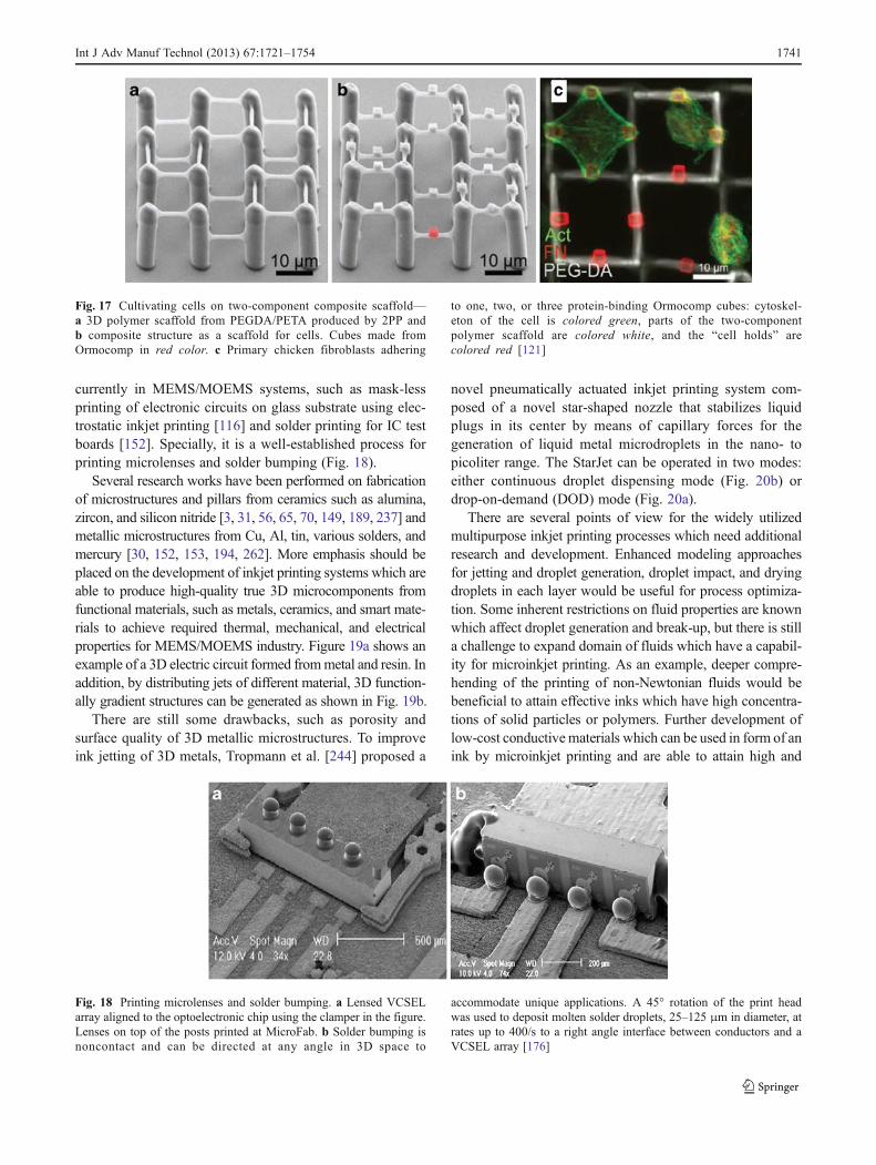
currently in MEMS/MOEMS systems, such as mask-lessprinting of electronic circuits on glass substrate using elec-trostatic inkjet printing [116] and solder printing for IC testboards [152]. Specially, it is a well-established process forprinting microlenses and solder bumping (Fig. 18).
Several research works have been performed on fabricationof microstructures and pillars from ceramics such as alumina,zircon, and silicon nitride [3, 31, 56, 65, 70, 149, 189, 237] andmetallic microstructures from Cu, Al, tin, various solders, andmercury [30, 152, 153, 194, 262]. More emphasis should beplaced on the development of inkjet printing systems which areable to produce high-quality true 3D microcomponents fromfunctional materials, such as metals, ceramics, and smart mate-rials to achieve required thermal, mechanical, and electricalproperties for MEMS/MOEMS industry. Figure 19a shows anexample of a 3D electric circuit formed frommetal and resin. Inaddition, by distributing jets of different material, 3D function-ally gradient structures can be generated as shown in Fig. 19b.
There are still some drawbacks, such as porosity andsurface quality of 3D metallic microstructures. To improveink jetting of 3D metals, Tropmann et al. [244] proposed a
novel pneumatically actuated inkjet printing system com-posed of a novel star-shaped nozzle that stabilizes liquidplugs in its center by means of capillary forces for thegeneration of liquid metal microdroplets in the nano- topicoliter range. The StarJet can be operated in two modes:either continuous droplet dispensing mode (Fig. 20b) ordrop-on-demand (DOD) mode (Fig. 20a).
There are several points of view for the widely utilizedmultipurpose inkjet printing processes which need additionalresearch and development. Enhanced modeling approachesfor jetting and droplet generation, droplet impact, and dryingdroplets in each layer would be useful for process optimiza-tion. Some inherent restrictions on fluid properties are knownwhich affect droplet generation and break-up, but there is stilla challenge to expand domain of fluids which have a capabil-ity for microinkjet printing. As an example, deeper compre-hending of the printing of non-Newtonian fluids would bebeneficial to attain effective inks which have high concentra-tions of solid particles or polymers. Further development oflow-cost conductivematerials which can be used in form of anink by microinkjet printing and are able to attain high and
Fig. 17 Cultivating cells on two-component composite scaffold—a 3D polymer scaffold from PEGDA/PETA produced by 2PP andb composite structure as a scaffold for cells. Cubes made fromOrmocomp in red color. c Primary chicken fibroblasts adhering
to one, two, or three protein-binding Ormocomp cubes: cytoskel-eton of the cell is colored green, parts of the two-componentpolymer scaffold are colored white, and the “cell holds” arecolored red [121]
Fig. 18 Printing microlenses and solder bumping. a Lensed VCSELarray aligned to the optoelectronic chip using the clamper in the figure.Lenses on top of the posts printed at MicroFab. b Solder bumping isnoncontact and can be directed at any angle in 3D space to
accommodate unique applications. A 45° rotation of the print headwas used to deposit molten solder droplets, 25–125 μm in diameter, atrates up to 400/s to a right angle interface between conductors and aVCSEL array [176]
Int J Adv Manuf Technol (2013) 67:1721–1754 1741

stable conductivity would be a great advancement in this area.Also, the applications of microinkjet printing in 3D micro-fabrication will expand with emersion of new jetting techni-ques such as electrostatic and better understanding of theprocess and utilization of efficient modeling techniques.
In the future, both the number and type of products fabri-cated using inkjet technology should increase, and the avail-ability and capabilities of inkjet-based prototyping andproduction tools should expand. Using inkjet-based methods,commercialization of products is in progress for DNA micro-arrays, color displays, electronics assembly, and photonicelements. Inkjet printing processes in combination with theprinted electronics technology makes it possible to manufac-ture real MEMS parts [125, 140, 229]. Future works may befocused on fabrication of true 3D high accuracy and improvedsurface finish part based on tailor made inks, using multi-material printing process. It is believed that using chemicallyetched able metal as support materials will be a worthwhileattempt toward improvement of fabrication of true 3D metalmicrostructures. As for ceramics, future works can be concen-trated on utilization of inkjet printing in innovative way formanufacturing various components, such as: multilayeredceramics (capacitors, sensors, and actuators), 3D electronicceramic components (high-temperature cofired ceramic andlow-temperature cofired ceramic), and conductive layers onceramic (photovoltaic components and thick film electronic).
6.2.3 3DP process
3DP process is easily adaptable to a variety of materialssystems, allowing the production of metallic/ceramic
microparts with novel compositions. This process currentlysuffers from some drawbacks such as inadequate surfacequality, minimum achievable feature size, and porosity buthas demonstrated good applicability for true 3D microfabri-cation. Both 3DP and inkjet printing processes are based onink jet technology, but 3DP takes the advantage of usingpowders as a substrate in each layer and as a result no supportmaterial is required for true 3D microfabrication. Moreover,3DP can be served in indirect routes such as ceramic molds tobuild microparts from variety of materials. There is alsopossibility to combine inkjet printing and 3DP process toproduce final microproducts. Especially inkjet printing oftailor made inks on the 3D surface produced already by 3DPprocess can open new opportunities. Figure 21 shows anexample of combination of Fcubic’s 3DP and inkjet printingprocess to produce final product. Achieved 3D electricalinterconnects is one of the most particular issues in micro-system integration. 3D electrical interconnects have alwaysbeen a challenge in electronics packaging. In this example,inkjet printing of silver (Ag) ink in 3D surface producedalready by 3DP process has been successfully demonstrated.Writing in 3D space is also persuaded by other microdeposi-tion processes such as aerosol jet process.
Further researches should be focused on increasing reso-lution of micro-3DP process and expanding range of mate-rials especially for MEMS application. The feasibility ofmanufacturing complex Ni–Ti parts by 3DP process hasalready been studied [157] and appropriate conditions forlayer deposition, printing, debinding, and sintering havebeen established. 3Dprinted Ni–Ti specimens exhibit shapememory behavior [32]. Nevertheless, further researches are
Fig. 19 a 3D electric circuitbuild from metal and resin andb a functional gradient structuremade of metal and resin [263]
Fig. 20 a A microtube with315-μm wall thickness printedby StarJet system in DODmode. The close-up view showsthe morphology of the poroussurface. b Coil-like structureprinted by StarJet system on aheated rotating substrate incontinuous mode (inset graph,top and side view of the star-shaped nozzle [136, 244]
1742 Int J Adv Manuf Technol (2013) 67:1721–1754
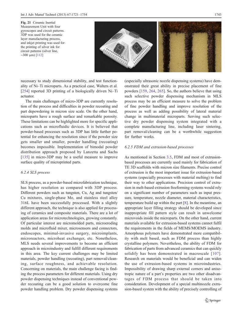
necessary to study dimensional stability, and test function-ality of Ni–Ti microparts. As a practical case, Walters et al.[254] reported 3D printing of a biologically driven Ni–Tiactuator.
The main challenges of micro-3DP are currently resolu-tion of the process and difficulties in powder recoating andpart depowdering in micron size scale. On the other hand,microparts have a rough surface and remarkable porosity.These limitations can be highlighted more for specific appli-cations such as microfluidic devices. It is believed thatpowder-based processes such as 3DP has little further po-tential for enhancing the resolution since if the powder sizegets smaller and smaller, powder handling (recoating)becomes impossible. Implementation of bimodal powderdistribution approach proposed by Lanzetta and Sachs[135] in micro-3DP may be a useful measure to improvesurface quality of microprinted parts.
6.2.4 SLS process
SLS process, as a powder-based microfabrication technique,has higher resolution as compared with 3DP process.Different powders such as tungsten, Cu, Ag and tungsten/Cu mixtures, single-phase Mo, and stainless steel alloy316L have been successfully processed. With a slightlydifferent approach, the technique is also applied for process-ing of ceramics and composite materials. There are a lot ofapplication areas for microtechnologies, growing constantly.Of particular interest are micromolded parts, microerodingmolds and microfluid mixer, microsensors and connectors,endoscopes, minimal-invasive surgery, microimplants,microreactors, microheat exchanger, etc. Nonetheless,MLS needs several improvements to become an efficientapproach in microindustry and fulfill different requirementsin this area. The key current challenges may be limitedmaterials, powder handling (recoating), part removal/clean-ing, surface roughness, and achievable resolution.Concerning on materials, the main challenge facing is find-ing the process parameters for different materials. Using drypowder dispensing techniques instead of conventional pow-der recoating can be a good solution to overcome finepowder handling problem. Dry powder dispensing systems
(especially ultrasonic nozzle dispensing systems) have dem-onstrated their great ability in precise placement of finepowders [159, 264, 265]. So, the authors believe that usingsuch selective powder dispensing mechanism in MLSprocess may be an efficient measure to solve the problemof fine powder handling and improve resolution of theprocess as well as adding possibility of lateral materialchange in multimaterial microparts. Serving such selec-tive dry powder dispensing system integrated with acomplete manufacturing line, including laser sintering,part removal/cleaning can be a worthwhile suggestionfor further works.
6.2.5 FDM and extrusion-based processes
As mentioned in Section 3.5, FDM and most of extrusion-based processes are currently used mainly for fabrication ofTE 3D scaffolds with micron size filaments. Precise controlof extrusion is the most important issue for extrusion-basedsystems (especially processes with material melting) to findtheir way to other applications. Precision control of extru-sion in melt-based extrusion freeforming systems would relyon a significant number of parameters such as input pres-sure, temperature, nozzle diameter, material characteristics,temperature build up within the part [8]. In the meantime, anappropriate layer filling strategy should be developed sinceinappropriate fill pattern style can result in unwelcomemicrovoids inside the microparts. On the other hand, currentmaterials available for extrusion-based systems cannot fulfilthe requirements in the fields of MEMS/MOEMS industry.Amorphous polymers have demonstrated more compatibil-ity with melt based, such as FDM process than highlycrystalline polymers. Nevertheless, the ability of FDM forfabrication of parts from advanced ceramics that can quicklysolidify has been demonstrated in macroscale [107].Research on materials would be beneficial and can widenthe use of extrusion-based systems in microindustries.Impossibility of drawing sharp external corners and aniso-tropic nature of a part’s properties are two other disadvan-tages of FDM process that should be taken intoconsideration. Development of a special multinozzle extru-sion-based system with the ability of precisely controlling of
Fig. 21 Ceramic InertialMeasurement Unit with fourgyroscopes and circuit patterns.3DP was used for the ceramiclayer manufacturing process,and inkjet printing was used forthe printing of silver ink forcircuit patterns (silver line,∼300 μm) [112]
Int J Adv Manuf Technol (2013) 67:1721–1754 1743

extrusion of variety of functional/composite materials wouldbe a worthwhile idea for further studies.
Recently, Schuurman et al. [212] used a hybrid bioplot-ting approach for fabrication of solid biodegradable material(polymers and ceramics) with cell-laden hydrogels thatcould combine favorable mechanical properties with cellspositioned at defined locations at high densities. Miranda etal. [179] used robocasting process to produce β-TCP scaf-folds with designed, 3D geometry and mesoscale porosityusing concentrated β-TCP inks with suitable viscoelasticproperties. The deposition was done in a nonwetting oil bathto prevent nonuniform drying during assembly. Dorj et al.[61] used robocasting process to produce a novel nanocom-posite scaffold made of chitosan and nanobioactive glass(nBG) retaining dual-pore structure. Robocasting was car-ried out under a cooled bath containing dry ice, to rapidlysolidify the scaffold as at ambient conditions, the dispensedsolution was hard to solidify. The chitosan/nBG nanocom-posite scaffolds were well constructed, with aligned macro-channelled pore structure.
Applications of the solvent-based extrusion freeformingrecently include fabrication of electromagnetic crystals[160], electromagnetic bandgap materials (EBG) [141, 161],millimetre-wave antenna [142], metamaterials [143], and car-bon scaffold for catalyst support [165]. Dielectric ceramicmaterials were used including alumina [160], quartz [162],LaO3 (Mg, 0.5 and Ti, 0.5), and TiO4 (Zr, 0.8 and Sn, 0.2)[161]. Wide range of filaments diameters from 150 [162] to500 µm [163] were used for fabrication of EBG with differentband gap. The effect of rheological properties of the paste onthe shape tolerance was investigated. When the extrudedfilament spans more than a critical distance, the filamentdeforms and leads to sagging [164]. Cylindrical woodpilestructure has been fabricated for narrow beam azimuthallyomni-directional millimeter-wave antenna [145, 146].
In recent years, researchers have focused on extendingdirect-write assembly process to biomedical applications.Using biocompatible inks, different 3D scaffolds and micro-vascular networks have been printed for tissue engineeringand cell culture. 3D HA scaffolds with 250 µm road width[175, 220], and 3D scaffolds composed of a gradient arrayof silk/HA filaments at size 200 µm were fabricated bydirect-write assembly [233]. 3D microperiodic hydrogelscaffolds composed of 1- [7] and 10-µm [217] rods wereproduced for guided cell growth by direct writing of a poly(2-hydroxyethyl methacrylate))-based ink through a gold-coated deposition micronozzle that is simultaneously photo-polymerized via UV illumination. Biocompatible silk opti-cal waveguides as fine as 5 µm was produced by direct-write assembly of a concentrated silk fibroin ink through amicronozzle into a methanol-rich coagulation reservoir[192]. Figure 22 [2] depicts some microstructures have beenproduced using advanced extrusion-based systems.
Cell-based printing techniques have also been intensivelyinvestigated in recent years and many innovativeapproaches such as organ bioprinting [180], laser writingof cells [210], bio-electrospraying [108], and biologicallaser printing [8] have surfaced to complement limitationsin scaffold-based tissue engineering. Organ bioprinting isdefined as the engineering of 3D living structures supportedby the self-assembly/organizing capabilities of cells deliv-ered through the application of AM techniques based onlaser, inkjet, or extrusion freeforming technologies [22]. Indirect bioprinting, balls or continues flows of bioinks aredeposited in well-defined topological patterns into biopaperlayers. The bioink building blocks typically have a sphericalor cylindrical shape and consist of single or multiple celltypes. In a post-processing step, the construct is transferredto a bioreactor and the bioink spheres are fused. The bio-paper, an inert and biocompatible hydrogel, can be removedafter construction in post-processing step [22]. Several ex-trusion-based systems such as 3D bioplotter described ear-lier can be served as a bioprinter, if sterile conditions can beacquired. However, it should be noted that, technologically,bioprinting using extrusion-based AM techniques is still inits infancy. Different living structures have been producedusing hydrogel structures containing viable cells, but thedesigns have been simple and isotropic, and mechanicalproperties were not satisfactory [174]. Thus, future worksin this area are mainly focused on effective utilization ofmultinozzle extrusion-based AM systems to produce livingmacro/microstructures with controlled compositions and im-proved accuracy.
6.2.6 LCVD process
LCVD system has been applied for deposition of variety ofmaterials such as carbon, silicon carbide, boron, boron ni-tride, and Mo onto various substrates including graphite,grafoil, zirconia, alumina, tungsten, and silicon [64]. Widerange of materials and complexity of microparts are themost significant advantages of LCVD process and makeLCVD a viable technology for further developments.Nevertheless, LCVD has a relatively high cost and systemcomplexity as compared with most micro-AM techniquesand is a high-temperature process. In addition, micropartsare built in a controlled-atmosphere chamber and this limitsability of LCVD process to make deposits on larger pre-existing structures [82]. LCVD is a high-resolution processbut no cost-effective production because of long buildingtime. One efficient approach is selective-area laser-deposition vapor-infiltration (SALDVI) technique in whichthe laser scans and heats the powder bed in a selectivemanner and solid material created from the gas is appliedto bind the heated powders material together [52]. SALDVIis much a faster process than LCVD, but microparts are
1744 Int J Adv Manuf Technol (2013) 67:1721–1754
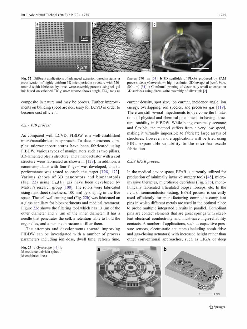
composite in nature and may be porous. Further improve-ments on building speed are necessary for LCVD in order tobecome cost efficient.
6.2.7 FIB process
As compared with LCVD, FIBDW is a well-establishedmicro/nanofabrication approach. To date, numerous com-plex micro/nanostructures have been fabricated usingFIBDW. Various types of manipulators such as two pillars,3D-lamented pleats structure, and a nanoactuator with a coilstructure were fabricated as shown in [129]. In addition, ananomanipulator with four fingers was developed, and itsperformance was tested to catch the target [128, 172].Various shapes of 3D nanorotors and bionanotools(Fig. 22) using C14H10 gas have been developed byMatsui’s research group [100]. The rotors were fabricatedusing nanosheet (thickness, 100 nm) by shaping in the freespace. The cell wall cutting tool (Fig. 22b) was fabricated ona glass capillary for bioexperiments and medical treatment.Figure 22c shows the filtering tool which has 13 μm of theouter diameter and 7 μm of the inner diameter. It has aneedle that penetrates the cell, a retention table to hold theorganelles, and a nanonet structure to filter them.
The attempts and developments toward improvingFIBDW can be investigated with a number of processparameters including ion dose, dwell time, refresh time,
current density, spot size, ion current, incidence angle, ionenergy, overlapping, ion species, and precursor gas [119].There are still several impediments to overcome the limita-tions of physical and chemical phenomena in having struc-tural stability in FIBDW. While being extremely accurateand flexible, the method suffers from a very low speed,making it virtually impossible to fabricate large arrays ofstructures. However, more applications will be tried usingFIB’s expandable capability to the micro/nanoscalefabrication.
6.2.8 EFAB process
In the medical device space, EFAB is currently utilized forproduction of minimally invasive surgery tools [45], micro-invasive therapies, microtissue debriders (Fig. 23b), mono-lithically fabricated articulated biopsy forceps, etc. In thefield of semiconductor testing, EFAB process is currentlyused efficiently for manufacturing composite-compliantpins in which different metals are used in the optimal placeto probe multiple integrated circuits in parallel. Compliantpins are contact elements that are great springs with excel-lent electrical conductivity and must-have high-reliabilitycontacts. A number of applications, such as capacitive pres-sure sensors, electrostatic actuators (including comb driveand gas-closing actuators) with increased height rather thanother conventional approaches, such as LIGA or deep
Fig. 22 Different applications of advanced extrusion-based systems: across-section of highly uniform 3D microperiodic structure with 520-nm rod width fabricated by direct-write assembly process using sol–gelink based on calcined TiO2; inset picture shows single TiO2 rods as
fine as 270 nm [63]. b 3D scaffolds of PLGA produced by PAMprocess, inset picture shows high-resolution 2D hexagonal (scale bars,500 µm) [31]. c Conformal printing of electrically small antennas on3D surfaces using direct-write assembly of silver ink [2]
Fig. 23 a Gyroscope [44]. bMicrotissue debrider (photo,Microfabrica Inc.)
Int J Adv Manuf Technol (2013) 67:1721–1754 1745

reactive ion etching, and fabrication of robust microstruc-tures (rather than brittle silicon) which are in direct contactwith the surrounding environment without any protectivepackaging have been successfully demonstrated. In addi-tion, this process can be used to create radio frequency(RF) building blocks such as fully coaxially shielded trans-mission lines, couplers, delay lines, patch antennas, andfilters. By combining such structures on a single chip usingthe EFAB process, it is possible to create sophisticated RFsystems on a chip, such as a phased array antenna [43]. Oneapplication area with considerable activity is the fabricationof very high-frequency passive components for compactmicrowave and millimeter-wave radar and communicationssystems (Fig. 14a). Figure 23a shows a gyroscope producedby EFAB process. Other possible microproducts can beactuators using hydraulics or pneumatics, valves and pumps,cams and followers, and linear and hydrostatic bearings[44].
EFAB process is a fast-growing 3D micromanufacturingtechnology. In 2010, Microfabrica introduced MICAFreeform as a second generation of EFAB process. MICAFreeform differs from EFAB in terms of materials and designrules: noble metal palladium, which is inert and offers bio- andMRI compatibility as well as radiopacity has been developedand minimum gap around a hinge can be 10 μm which was30 μm in EFAB. However, there are still some aspects thatneed to be improved. There are currently limitations for max-imum number of layers in a part (maximum of 50 layers),producing a maximum part thickness of about 1.25 mm.Moreover, release holes should be designed for completeremoval of support materials where internal channels or mul-tiple components are involved. On the other hand, stair-stepeffect makes some difficulties in some cases and the gapbetween moving parts in assemblies cannot be smaller thanminimum layer thickness. To date, the ability of EFAB toproduce microassemblies that include mechanical elementsas well as electrically active components such as capacitivesensors and electrostatic actuators has been demonstrated.Electromagnetism or shape memory-based sensing and actu-ation systems are also possible and are expected to be devel-oped in the future [44]. The feasibility of fabricating devicesusing EFAB from Ni-Ti has already been demonstrated.Moreover, there exists some limited experience with palladi-um–Co, stainless steel, Pt, Au, Ag, as well as higher strengthNi-based alloys [43]. Full-commercial development of any ofthese metals will require the investment of time and resources.Thus, future development will depend on technical require-ments and market opportunities.
6.3 Future trends
Most of the MEMS fabrication methods are adopted fromstandard IC technology. Themost commonMEMS fabrication
techniques are: bulk micromachining, surface micromachin-ing, and LIGA. These planar micromanufacturing processeshave achieved commercial success in different sectors, such asindustrial sensor (e.g., pressure sensors), inertial sensor (e.g.,accelerometers and rate gyros), and telecommunications (e.g.,compliant structures for fiber waveguide alignment, variableoptical attenuators, and cross-connect switches). However,there are still some essential limitations that have slowed theadoption and development of MEMS-based systems usingthese planar manufacturing processes [115]:
1. The structures created by these processes are inherentlylimited to 2D (e.g., inch worm and comb drive) or to“2.5D” (e.g., self-erecting mirrors) structures that can beerected from 2D structures. True 3D mechatronicsimplemented this way requires, often tricky, assemblyof multiple 2D MEMS components.
2. The nonrecurring engineering costs such as mask gen-eration are high, and this makes it difficult for emergingcompanies with comparatively small volumes to deploythe technology.
3. The delivery times are long—often 12–15 weeks—extending the “time-to-money” by stretching design,verification, and validation cycles.
4. The manufacturing processes are not truly scalable. Forinstant, extending the number of layers in surface micro-machining process from four to five layers (extendingthe height of the machine from 10 to 12 μm) could takemonths or years due to the impact of thermal cyclesduring deposition of the fifth layer on the residualstresses in layers 1–4 and the corresponding effect ofthese residual stresses on layer 5.
5. The packaging cost of these components is high.Integration of planar MEMS with optical components(fiber, array waveguides, etc.) and housing often repre-sents 80 % of the manufacturing cost of a microsystem.
3D micro-AM processes can be considered as apromising alternative to assuage the influence of theabove items and bring MEMS/MOEMS technologies asignificant step further. In addition to 3D design, thespeed of micro-AM processes provides profits to boththe microproduct development process and to manufac-turing. In particular, microsystems can be prototypedfaster and this results in lessening microproduct devel-opment time and allowing design iteration and optimi-zation. Serious design modifications can be donemidway in the product development process withoutany change to the microfabrication technology. In addi-tion, micro-AM systems can be applied directly for finalmicroproduct manufacturing. In this way, “rapid micro-manufacturing” as a new terminology in micomanufac-turing field can be more accessible using 3D micro-AMtechnologies. Micro-AM processes have shown their
1746 Int J Adv Manuf Technol (2013) 67:1721–1754

high potential for RM in microscale due to some sig-nificant aspects such as cost efficiency for individual-ized or small series production and no need to maskpreparation like conventional lithographic-based process-es, etc. Thus, particular emphasis in the future will beplaced on improving 3D micro-AM systems and inte-gration of manufacturing and the packaging/assemblingprocesses to reach the concept of rapid micromanufac-turing. MSL is currently the most favorable processamong other micro-AM technologies for this goal.MicroTEC is a recognized company with the scope of shiftingtoward rapid micromanufacturing using MSL process and hasdemonstrated interesting results in this way. MicroTEC’sRMPD technologies are currently used for rapid micromanu-facturing of serial parts (1,000–5,000 and more parallel) invariety of materials like plastic or sol–gel. MicroTEC’s unique3D-CSP technology is used to integrate, interconnect, andprotect bare dies or other microelectronic elements to get acomplete multifunctional system. No wire bonding is needed;interconnection is realized by microstructured metal layers;3D ultrahigh-density integration is possible; and cooling chan-nels can be integrated to cool hot spots [83]. 3D-CSP tech-nology in combination with RMPD makes an efficient rapidmicromanufacturing approach which is applied for manyapplications, such as life science (e.g., lab on a chip micro-fluidics), sensor technology (e.g., food control solutions),consumer electronics (e.g., very slim connectors for smartcarts), micromechanical parts for metrology tools, etc.Figure 24 shows examples of microTEC’s RMPD and 3D-CSP applications in rapid micromanufacturing of plastic partsand microsystems.
Today, markets are looking for energy efficient, fast, andflexible approaches, so conventional micromanufacturingprocesses are not efficient tools in today’s micromanufactur-ing. Prosperity in new applications will increasingly dependon understanding the strengths and weaknesses of a varietyof micro-AM fabrication approaches and using the rightfabrication technology or combination of technologies fora given set of requirements. As a consequence of what was
discussed above, it is believed that future works will bemainly concentrated on making micro-AM processes morefavorable for rapid micromanufacturing through improvingprocesses and integration of fabrication with assembling andpackaging.
7 Conclusions
Many techniques have been developed up to now to respondthe demand for high-quality 3D microcomponents used inMEMS and microengineering areas. The additive processeshave been identified as a progressive and effective 3Dmicrofabrication technology during two decade evolution.This paper presented a review on the key micro-AM pro-cesses used to build functional and true 3D microstructures.The micro-AM systems have been continuously enhancedbut more studies are still required to improve the micro-AMsystems and the quality of the 3D microstructures. Amongmicro-AM systems, MSL and EFAB processes have dem-onstrated more acceptable results in 3D microfabricationarea as compare with other discussed systems.
Acknowledgments The authors would like to thank Mr. UrbanHarrysson of Fcubic AB and Mrs. Andrea E. Reinhardt of microTECGmbH for contributions in the preparation of this paper.
References
1. Accoto D, Carrozza MC, Dario P (2000) Modelling of micro-pumps using unimorph piezoelectric actuators and ball valves. JMicromech Microeng 10:277–281
2. Adams JJ, DUOSS EB, Malkowski TF, Motala MJ, Ahn BY,Nuzzo RG, Bernhard JT, Lewis JA (2011) Conformal printing ofelectrically small antennas on three-dimensional surfaces. AdvMater 23(11)):1335–1340
3. Ainsley C, Reis N, Derby B (2002) Freeform fabrication bycontrolled droplet deposition of powder filled melts. J Mater Sci37:3155–3161
4. Alting L, Kimura F, Hansen HN, Bissacco G (2003) Microengineering. CIRP Ann Manuf Technol 52:635–657
Fig. 24 a Complete 3D-CSP-based transceiver module in smallestspace (5.2×5.2×2.2 mm3) for wireless solutions, b) 3D-coil variationswith RMPD and 3D-CSP for wireless energy supply and
communication, c high-volume-production of plastic microgears usingRMPD technology, diameters at 828 and 1,200 μm [177]
Int J Adv Manuf Technol (2013) 67:1721–1754 1747

5. Ang TH, Sultana FSA, Hutmacher DW, Wong YS, Fuh JYH, MoXM, Loh HT, Burdet E, Teoh SH (2002) Fabrication of 3D chito-san-hydroxyapatite scaffolds using a robotic dispensing system.Materials Science & Engineering C-Biomimetic andSupramolecular Systems 20:35–42
6. Arcaute K, Mann B, Wicker R (2010) Stereolithography of spa-tially controlled multi-material bioactive poly(ethylene glycol)scaffolds. Acta Biomaterialia 6:1047–1054
7. Barry RA, Shepherd RF, Hanson JN, Nuzzo RG, Wiltzius P,Lewis JA (2009) Direct-Write Assembly of 3D HydrogelScaffolds for Guided Cell Growth. Adv Mater 21:2407–2410
8. Barron, JA, Wu P, Ladouceur HD, Ringeisen BR (2004)Biological laser printing: a novel technique for creating hetero-geneous 3-dimensional cell patterns. Biomed Microdevices6:139–147
9. Bartolo PJ (2011) Stereolithography: materials, processes andapplications. Springer, London
10. Bartolo PJ, Gaspar J (2008) Metal filled resin for stereolithogra-phy metal part. CIRP Ann Manuf Technol 57:235–238
11. Becker EW, Ehrfeld W, Hagmann P, Maner A, Munchmeyer D(1986) Fabrication of microstructures with high aspect ratios andgreat structural heights by synchrotron radiation lithography,galvanoforming, and plastic moulding (LIGA process).Microelec Eng 4:35–56
12. Beluze L, Bertsch A, Renaud P (1999) Microstereolithography: anew process to build complex 3D objects. In: SPIE symposiumon design, test and microfabrication of MEMs/MOEMs, Paris,France
13. Bertsch A, Bernhard P, Vogt C, Renaud P (2000) Rapid proto-typing of small size objects. Rapid Prototyping J 6:259–266
14. Bertsch A, Heimgartner S, Cousseau P, Renaud P (2001). 3Dmicromixers—downscaling large-scale industrial static mixers.In: The 14th IEEE International Conference on Micro ElectroMechanical Systems (MEMS2001), Interlaken, Switzerland. pp.507–510
15. Bertsch A, Heimgartner S, Cousseau P, Renaud P (2001) Staticmicromixers based on large-scale industrial mixer geometry. LabChip 1:56–60
16. Bertsch A, Jiguet S, Renaud P (2004) Microfabrication of ceram-ic components by microstereolithography. J MicromechMicroeng 14:197–203
17. Bertsch A, Lorenz H, Renaud P (1998). Combining microstereo-lithography and thick resist UV lithography for 3D microfabrica-tion. In: Proceedings of the IEEE International Conference onMicro Electro Mechanical Systems (MEMS). pp. 18–23.
18. Bertsch A, Lorenz H, Renaud P (1999) 3D microfabrication bycombining microstereolithography and thick resist UV lithogra-phy. Sensor Actuator Phys 73:14–23
19. Bertsch A, Zissi S, Jezequel JY, Corbel S, Andre JC (1997)Microstereophotolithography using a liquid crystal display asdynamic mask generator. Microsyst Technol 3:42–47
20. Bertsch A, Jezequel YJ, Andre JC (1997) Study of the spatialresolution of a new 3D micro fabrication process; the microster-eolithography using a dynamic mask-generator technique. JPhotochem Photobiol Chem 107:275–282
21. Bhushan B (2007) Handbook of nanotechnology. Springer, NewYork
22. Billiet T, Vandenhaute M, Schelfhout J, Van Vlierberghe S,Dubruel P (2012) A review of trends and limitations in hydro-gel-rapid prototyping for tissue engineering. Biomaterials33:6020–6041
23. Bredt, J.F., Anderson, T.C., Russell, D.B., 2002. Three dimen-sional printing materials system. US Patent 6,416,850. US Patentand Trademark Office, Z Corporation
24. Brinksmeier E, Riemer O, Stern R (2001). Machining of preci-sion parts and microstructures. In: Proceedings of the 10th
International Conference on Precision Engineering (ICPE),Yokohama, Japan, 18–20 July. pp. 3–11
25. Broer DJ, Mol GN, Challa G (1991) In-situ photopolymerization oforiented liquid-crystalline acrylates. Makromol Chem 192:59–74
26. Brousseau EB, Dimov SS, Pham DT (2010) Some recent advan-ces in multi-material micro- and nano-manufacturing. Int J AdvManuf Technol 47:161–180
27. Butler EJ, Folk C, Cohen A, Vasilyev NV, Chen R, del Nido PJ,Dupont PE (2011). Metal MEMS tools for beating-heart tissueapproximation. In: 2011 IEEE International Conference onRobotics and Automation, Shanghai, China
28. Buyer ’s guide, envisionTEC GmbH. Available fromwww.envisiontec.de
29. Campbell AN, Tanner DM, Soden JM, Stewart DK, Doyle A,Adam E, Gibson M, Abramo M (1997). Electrical and chemicalcharacterization of FIB-deposited insulators. In: Proceedings ofthe 23 International Symposium on Testing and Failure Analysis.pp. 223–230.
30. Cao W, Miyamoto Y (2006) Freeform fabrication of aluminumparts by direct deposition of molten aluminum. J Mater ProcessTechnol 173:209–212
31. Cappi B, Özkol E, Ebert J, Telle R (2008) Direct inkjet printing ofSi3N4: characterization of ink, green bodies and microstructure. JEur Ceram Soc 28:2625–2628
32. Carreño-Morelli E, Martinerie S, Bidaux JE (2007) Three-dimensional printing of shape memory alloys. Mater Sci Forum534–536:477–480
33. Carrozza MC, Croce N, Magnani B, Dario P (1995) Apiezoelectric-driven stereolithography-fabricated micropump. JMicromech Microeng 5:177–179
34. Cawley JD (1999) Solid freeform fabrication of ceramics. CurrOpin Solid State Mater Sci 4:483–489
35. Cesarano J (1999) A review of robocasting technology. In: DimosD, Danforth SC, Cima MJ (eds) Solid Freeform and AdditiveFabrication. Materials Research Society, Warrendale
36. Charmeux JF, Minev R, Dimov S, Minev E, Su S, Harrysson U(2008). Capability study of the Fcubic direct shell process forcasting micro-components. 4M Cross Divisional Report. CardiffUniversity, Cardiff
37. Chatwin CR, Farsari M, Huang S, Heywood HI, Birch PM, YoungRCD, Richardson JD (1998) UV microstereolithography system thatuses spatial light modulator technology. Appl Optic 37:7514–7522
38. Chen RT, Brown ER, Singh RS (2004). A compact 30 GHZ lowloss balanced hybrid coupler fabricated using micromachinedintegrated coax. In: Proceedings 2004 IEEE Radio and WirelessConference, Atlanta, GA
39. Cheng YL, Lin JH, Lai JH, Ke CT, Huang YC (2005).Development of dynamic mask photolithography system. In:Proceedings of the 2005 IEEE International Conference onMechatronics, Taipei, Taiwan. pp. 467–471
40. Choi JW, Ha YM, Won MH, Choi KH, Lee SH (2005).Fabrication of 3-dimensional microstructures using dynamicimageprojection. In: Proceedings of International Conferenceon Precision Engineering and Micro/Nano Technology in Asia(ASPEN 2005), Shenzhen, China. pp. 472–476
41. Chua CK, Leong KF, Lim CS (2010) Rapid prototyping: princi-ples and applications, 3rd edn. World Scientific, Singapore
42. Clare AT, Chalker PR, Davies S, Sutcliffe CJ, Tsopanos S (2008)Selective laser melting of high aspect ratio 3D nickel–titaniumstructures two way trained for MEMS applications. Int J MechMater Des 4:181–187
43. Cohen A, (2004). Going beyond silicon MEMS with EFABTechnology. White paper. Microfabrica Inc., Burbank
44. Cohen A, (2005). EFAB Technology: unlocking the potential ofminiaturized medical devices. EVP, Technology and CTO.Microfabrica Inc., Burbank
1748 Int J Adv Manuf Technol (2013) 67:1721–1754

45. Cohen A, Chen, R (2007). Microfabricated tissue removal instru-ments for minimally-invasive procedures. In: 19th InternationalConference of the Society for Medical Innovation and Technology,Sendai, Japan
46. Cohen A, Chen R, Frodis U, Wu MT, Folk C (2010) Microscalemetal additive manufacturing of multi-component medical devi-ces. Rapid Prototyping J 16:209–215
47. Cohen A, Frodis U, Zhang G, (1998). EFAB: batch production offunctional, fully-dense metal parts with micron-scale features. In:Solid Freeform Fabrication Symposium Proceedings, TheUniversity of Texas, Austin
48. Cohen A, Kruglick E (2006) EFAB technology and applications.In: Gad-el-Hak M (ed) The MEMS handbook, vol 2nd. CRCPress, Boca Raton
49. Cohen A, Wooden S (2005). Monolithic 3-D microfabrication ofmechanisms with multiple independently-moving parts. In:Proceedings of IMECE2005: 2005 ASME InternationalMechanical Engineering Congress and Exposition, Florida.
50. Cohen A, Zhang G, Tseng F, Frodis U, Mansfeld F, Will P (1999).EFAB: rapid, low-cost desktop micromachining of high aspectratio true 3-D MEMS. In: Proceedings of the IEEE InternationalMEMS 99 Conference. pp. 244–251
51. Crivello JV (1999) The discovery and development of onium saltcationic photoinitiators. J Polymer Sci Polymer Chem 37:4241–4254
52. Crocker JE, Harrison S, Sun LLL, Marcus HL (1998) UsingSALDVI and SALD with multi-material structures. J Miner MetMater Soc 50:21–23
53. Cumpston BH, Ananthavel SP, Barlow S, Dyer DL, Ehrlich JE,Erskine LL, Heikal AA, Kuebler SM, Lee IYS, McCord-MaughonD, Qin J, Röckel H, Rumi M,Wu XL,Marder SR, Perry JW (1999)Two-photon polymerization initiators for three-dimensional opticaldata storage and microfabrication. Nature 398:51–54
54. Day D, Gu M (1999) Use of two-photon excitation for erasablere-writable three-dimensional bit optical data storage in a photo-refractive polymer. Opt Lett 24:948–950
55. Debaes C, Vervaeke M, Volckaerts B, Van Erps J, Desmet L,Ottevaere H, Vynck P, Gomez V, Hermanne A, Thienpont H(2005) Low-cost micro-optical modules for board level opticalinterconnections. IEEE LEOS Newsletter 19:12–14
56. Derby B, Reis N (2003) Inkjet printing of highly loaded partic-ulate suspensions. MRS Bull 28:815–818
57. Deubel M, Von Freymann G, Wegener M, Pereira S, Busch K,Soukoulis CM (2004) Direct laser writing of three-dimensionalphotonic-crystal templates for telecommunications. Nat Mater3:444–447
58. Deubel M, Wegener M, Linden S, Von Freymann G, John S(2006) 3D-2D-3D photonic crystal heterostructures fabricatedby direct laser writing. Optic Lett 31:805–807
59. Dimov, SS, Matthews CW, Glanfield A, Dorrington PA (2006).Roadmapping study in multi-material micro manufacture. In:Proceedings of the Second International Conference on Multi-material Micromanufacture, 4M2006, Grenoble, France, 20–22September, pp. xi–xxv
60. Doraiswamy A, Jin C, Narayan RJ, Mageswaran P, Mente P,Modi R, Auyeung R, Chrisey DB, Ovsianikov A, Chichkov B(2006) Two photon induced polymerization of organic–inorganichybrid biomaterials for microstructured medical devices. ActaBiomaterialia 2:267–275
61. Dorj B, Park JH, Kim HW (2012) Robocasting chitosan/nano-bioactive glass dual-pore structured scaffolds for bone engineer-ing. Mater Lett 73:119–122
62. Dufaud O, Corbel S (2003) Oxygen diffusion in ceramic suspen-sions for stereolithography. Chem Eng J 92:55–62
63. Duoss EB, Twardowski M, Lewis JA (2007) Sol–gel Inks forDirect-Write Assembly of Functional Oxides. Adv Mater 19(21):3485–3489
64. Duty C, Jean D, Lackey WJ (2001) Laser chemical vapor depo-sition: materials, modeling, and process control. Int Mater Rev46:271–287
65. Ebert J, Özkol E, Zeichner A, Uibel K, Weiss O, Koops U, TelleR, Fischer H (2009) Direct inkjet printing of dental prosthesesmade of zirconia. J Dent Res 88:673–676
66. Ebert R, Regenfuss P, Hartwig L, Klötzer S, Exner H, (2003). Processassembly for μm-scale SLS, reaction sintering, and CVD. In: 4thInternational Symposium on Laser Precision Microfabrication.Proceedings of SPI vol. 5063, S.183–188
67. Edinger K (2002) Focused ion beam for direct writing. In: PiqueA, Chrisey DB (eds) Direct write technologies for rapid proto-typing applications. Academic, New York, pp 347–383
68. Edinger K, Melngailis J, Orloff J (1998) Study of precursor gasesfor focused ion beam insulator deposition. J Vac Sci Tech B16:3311–3314
69. Ehrfeld W, Schmidt A (1998) Recent developments in deep X-raylithography. J Vac Sci Technol B 16:3526–34
70. Evans J, Yang S (2009) Solid freeforming and combinatorialresearch. Tsinghua Sci Technol 14(S1):94–99
71. Exner H, Horn M, Streek A, Hartwig L, Ebert R (2005) Firstresults in laser micro sintering of ceramic materials. EuropeanCongress on Advanced Materials and Processes, Prague
72. Exner H, Horn M, Streek A, Ullmann F, Hartwig L, Regenfuß P,Ebert R (2008). Laser micro sintering: a new method to generatemetal and ceramic parts of high resolution with sub-micrometerpowder. In: Virtual and physical prototyping, vol 3. Taylor &Francis, New York. pp. 3–11
73. Exner H, Regenfuss P, Hartwig L, Klötzer S, Ebert R (2003).Selective laser micro sintering with a novel process. In: 4thInternational Symposium on Laser Precision Microfabrication.Proceedings of SPI, vol. 5063, S.145–151.
74. Farrer RA, LaFratta CN, Li L, Praino J, Naughton MJ, SalehBEA, Teich MC, Fourkas JT (2006) Selective functionalization of3-D polymer microstructures. J Am Chem Soc 128:1796–1797
75. Fedorovich NE, Oudshroon MH, Geemen D, Hennink WE,Alblas J, Dhert WJA (2009) The effect of photopolymerizationon stem cells embedded in hydrogels. Biomaterials 30:344–353
76. Formanek F, Takeyasu N, Tanaka T, Chiyoda K, Ishikawa A,Kawata S (2006) Three-dimensional fabrication of metallic nano-structures over large areas by two-photon polymerization. OptExpress 14:800–809
77. Foulon F, StukeM (1993) Argon-ion laser direct-write Al depositionfrom trialkylamine alane precursors. Appl Physic A 56:283–289
78. Freymann GV, Ledermann A, Thiel M, Staude I, Essig S, BuschK, Wegener M (2010) Three-dimensional nanostructures for pho-tonics. Adv Funct Mater 20:1038–1052
79. Galajda P, Ormos P (2001) Complex micromachines producedand driven by light. Appl Phys Lett 78:249–251
80. Gaspar J, Bartolo PJ, Duarte FM (2008) Cure and rheologicalanalysis of reinforced resins for stereolithography. Mater SciForum 587–588:563–567
81. Gebhardt A (2003) Rapid prototyping. Hanser GardnerPublications, Inc., Cincinnati (originally published in German)
82. Gibson I, Rosen DW, Stucker B (2010) Additive manufacturingtechnologies. Springer, New York
83. Gotzen R, Reinhardt A (2008) High volume production by RM:challenges and solutions for small parts and MEMS. Internationalconference on additive technologies. Ptuj, Slovenia
84. Greulich M, Greul M, Pintat T (1995) Fast, functional prototypesvia multiphase jet solidification. Rapid Prototyping J 1:20–25
85. Grida I, Evans JRG (2003) Extrusion freeforming of ceramicsthrough fine nozzles. J Eur Ceram Soc 23:629–635
86. Guo R, Li Z, Jiang Z, Yuan D, Huang W, Xia A (2005) Log-pilephotonic crystal fabricated by two-photon photopolymerization. JOpt A: Pure Appl Opt 7:396–699
Int J Adv Manuf Technol (2013) 67:1721–1754 1749

87. Guo R, Xiao S, Zhai X, Li J, Xia A, Huang W (2006) Micro lensfabrication by means of femtosecond two photon polymerization.Opt Express 14:810–816
88. Ha YM, Park IB, Kim HC, Lee SH (2010) Three-dimensionalmicrostructure using partitioned cross-sections in projectionmicrostereolithography. Int J Precis Eng Manuf 11:335–340
89. Hadipoespito G, Yang Y, Choi H, Ning G, Li X, (2003). Digitalmicromirror device based microstereolithography for micro struc-tures of transparent photopolymer and nanocomposites. In:Proceedings of the 14th Solid Freeform FabricationSymposium, Austin, TX. pp. 13–24
90. Haferkamp H, Ostendorf A, Becker H, Czerner S, Stippler P(2004) Combination of Yb:YAG-disc laser and roll-based powderdeposition for the micro-laser sintering. J Mater Process Tech149:623–626
91. Hasegawa T, Nakashima K, Omatsu F, Ikuta K (2008) Multi-directional micro switching valve chip with rotary mechanism.Sensor Actuator Phys 143:390–398
92. Hatashi T (2000). Direct 3D forming using TFT LCD mask. In:Proceedings of the 8th International Conference on RapidPrototyping, Tokyo, Japan. pp. 172–177
93. Heller C, Schwentenwein M, Russmueller G, Varga F, Stampfl J,Liska R (2009) Vinyl esters: low cytotoxicity monomers for thefabrication of biocompatible 3D scaffolds by lithography basedadditivemanufacturing. J Polymer Sci Polymer Chem 47:6941–6954
94. Hill RT, Lyon JL, Allen R, Stevenson KJ, Shear JB (2005)Aqueous microfabrication of bioelectronic architectures. J AmChem Soc 127:10707–10711
95. Hoffmann P, Melngailis J, Michler J (2000). Focused ion beaminduced deposition of gold and rhodium. In: Proceedings of theMaterials Research Society Symposium, vol. 624. pp. 171–175
96. Hon KKB, Li L, Hutchings IM (2008) Direct writing technology—advances and developments. CIRP Ann Manuf Technol57:601–620
97. Huang YM, Jiang CP (2003) Numerical analysis of mask typestereolithography process using dynamic finite element method.Int J Adv Manuf Technol 21:649–655
98. Huang YM, Jeng JY, Jiang, CP, Wang JC (2001). Computersupported force analysis and layer imagine for masked rapidprototyping system. In: Proceedings of the 6th InternationalConference on Computer Supported Cooperative Work inDesign, Ontario, Canada. pp. 562–567
99. Hung-Jen Y, Ching-Shiow T, Shan-Hui H, Ching-Lin T (2009)Evaluation of chondrocyte growth in the highly porous scaffoldsmade by fused deposition manufacturing (FDM) filled with typeII collagen. Biomed Microdevices 11:615–624
100. Igaki J, Kometani R, Nakamatsu K, Kanda K, Haruyama Y,Ochiai Y (2006) Three-dimensional rotor fabrication byfocused-ion-beam chemical-vapor deposition. MicroelectronEng 83:1221–1226
101. Ikuta K, Hasegawa T, Adachi T (2001). The optimized SMAmicro-pump chip applicable to liquids and gases. In: Thansducers’01Eurosensors XV Workshop, Munich, Germany
102. Ikuta K, Hasegawa T, Adachi T, Maruo S (2000). Fluid drivechips containing multiple pumps and switching valves for bio-chemical IC family. In: 13th IEEE International Conference onMicroelectro Mechanical Systems (MEMS 2000), Miyazaki,Japan. pp. 739–744
103. Ikuta K, Hirowatari K (1993). Real three-dimensional microfabri-cation using stereolithography and metal molding. In: Proceedingsof the IEEE international Workshop on MicroelectromechanicalSystems (MEMS ‘93), Fort Lauderdale. pp. 42–47
104. Ikuta K, Maruo S, Kojoma S (1993). New microstereo lithogra-phy for freely movable 3D microstructure. In: Proceedings of theIEEE international Workshop on MicroelectromechanicalSystems (MEMS ‘93), Fort Lauderdale. pp. 290–295
105. Ikuta K, Ogata T, Tsubio M, Kojima S, (1996). Development ofmass productive microstereolithography. In: Proceedings of theIEEE international Workshop on MicroelectromechanicalSystems (MEMS), San Diego. pp. 301–305
106. Ikuta K, Sasaki Y, Maegawa H, Maruo S, (2002). Microultrasonichomogenizer chip made by hybrid microstereolithography. In:Symposium on Micrototal Analysis Systems (MicroTAS’02)Conference. Kluwer, Norwell.
107. Jafari MA, Han W, Mohammadi F (2000) A novel system forfused deposition of advanced multiple ceramics. RapidPrototyping J 6:161–175
108. Jayasinghe SN (2007) Bio-electros prays: The development of apromising tool for regenerative and therapeutic medicine.Biotechnol J 2:934–937
109. Jiang XS, Qi LH, Luo J, Huang H, Zhou JM (2010) Research onaccurate droplet generation for micro-droplet deposition manu-facture. Int J Adv Manuf Technol 49:535–541
110. Jiguet S, Bertsch A, Renaud P (2002). Microstereolithographyand ceramic composite three-dimensional parts. In: Proceedingsof the Shaping II conference, Gent, Belgium
111. Johander P, Eberhard W, Necula D, Haasl S, Jung E (2007).Three-dimensional electronics packaging and interconnection3D PACK. 4M Cross Divisional Report. Cardiff University,Cardiff. pp. 8–22.
112. Johander P, Haasl S, Persson K, Harrysson U (2007). Layermanufacturing as a generic tool for microsystem integration. In:4M2007 Conference Proceedings, Borovets, Bulgaria.
113. Johander P, Harrysson U, Kaufmann U, Ritzhaupt-Kleissl HJ,(2005). Direct manufacture of ceramic micro components withlayered manufacturing methods. In: 4M Conference, Karlsruhe,Germany
114. Kalita SJ, Bose S, Hosick HL, Bandyopadhyay A (2003)Development of controlled porosity polymer-ceramic composite scaf-folds via fused deposition modeling. Materials Science &Engineering C-Biomimetic and Supramolecular Systems 23:611–620
115. Karam RM, Casler RJ (2003). A new 3D, direct-write, sub-micron microfabrication process that achieves true optical,mechatronic and packaging integration on glass-ceramic sub-strates. White paper, Invenios, Inc
116. Kawamoto H (2007). Electronic circuit printing, 3D printing andfilm formation utilizing electrostatic inkjet technology. In:International Conference on Digital Printing Technologies andDigital Fabrication, Anchorage, Alaska. pp. 961–964
117. Kawata S, Sun HB, Tanaka T, Takada K (2001) Finer features forfunctional microdevices. Nature 412:697–698
118. Khalil S, Nam J, Sun W (2005) Multi-nozzle deposition forconstruction of 3D biopolymer tissue scaffolds. RapidPrototyping J 11:9–17
119. Kim CS, Ahn SH, Jang DY (2012) Review: developments inmicro/nanoscale fabrication by focused ion beams. Vacuum86:1014–1035
120. Kim DS, Lee IH, Kwon TH, Cho DW (2004) A barrier embeddedKenics micromixer. J Micromech Microeng 14:1294–1301
121. Klein F, Richter B, Striebel T, Franz CM, Freymann GV, WegenerM, Bastmeyer M (2011) Two-component polymer scaffolds forcontrolled three-dimensional cell culture. Adv Mater 23:1341–1345
122. Klein S, Barsella A, Leblond H, Bulou H, Fort A, Andraud C,Lemercier G, Mulatier JC, Dorkenoo K (2005) One-step wave-guide and optical circuit writing in photopolymerizable materialsprocessed by two-photon absorption. Appl Phys Lett 86:211118(1)–211118(3)
123. Klosterman DA, Chartoff RP, Osborne NR, Graves GA, LightmanA, Han GW, Bezeredi A, Rodrigues S, Pak S, Kalmanovich G,Dodin L, Tu S (1998) Direct fabrication of ceramics, CMCs byrapid prototyping. Am Ceram Soc Bull 77:69–74
1750 Int J Adv Manuf Technol (2013) 67:1721–1754

124. Ko SH, Chung J, Hotz N, NamKH, Grigoropoulos CP (2010)Metalnanoparticle direct inkjet printing for low-temperature 3D micrometal structure fabrication. JMicromechMicroeng 20:125010 (7 pp)
125. Ko SH, Pan H, Grigoropoulos CP, Luscombe CK, Fréchet J,Poulikakos D (2007) All-inkjet-printed flexible electronics fabri-cation on a polymer substrate by low-temperature high-resolutionselective laser sintering of metal nanoparticles. Nanotechnology18:345202
126. Kobayashi K, Ikuta K (2005). Development of free surfacemicrostereolithography with ultra high resolution to fabricatehybrid 3-D microdevices. In: IEEE International Symposium onMicro-nano Mechatronics and Human Schience
127. Kometani R, Funabiki R, Hoshino T, Kanda K, Haruyama Y,Kaito T (2006) Cell wall cutting tool and nano-net fabrication byFIB-CVD for subcellular operations and analysis. MicroelectronEng 83:1642–1645
128. Kometani R, Hoshino T, Kondo K, Kanda K, Haruyama Y, KaitoJ (2005) Performance of nanomanipulator fabricated on glasscapillary by focused ion-beam chemical vapor deposition. J VacSci Technol B 23:298–301
129. Kometani R, Morita T, Watanabe K, Hoshino T, Kondo K, KandaK (2004) Nanomanipulator and actuator fabrication on glasscapillary by focused-ion beam-chemical vapor deposition. J VacSci Technol B 22:257–263
130. Lai WH, Chen CC (2005) Effect of oxidation on the breakup andmonosized droplet generation of the molten metal jet. AtomizSpr15:81–102
131. Lam CXF, Mo XM, Teoh SH, Hutmacher DW (2002) Scaffolddevelopment using 3D printing with a starch-based polymer.Mater Sci Eng C 20:49–56
132. Lan PX, Lee JW, Seol YJ, Cho DW (2009) Development of 3DPPF/DEF scaffolds using micro-stereolithography and surfacemodification. J Mater Sci Mater Med 20:271–279
133. Landers R, Hübner U, Schmelzeisen R, Mülhaupt R (2002) Rapidprototyping of scaffolds derived from thermoreversible hydrogelsand tailored for applications in tissue engineering. Biomaterials23:4437–4447
134. Landers R, Mühlhaupt R (2000) Desktop manufacturing of com-plex objects, prototypes and biomedical scaffolds by means ofcomputer-assisted design combined with computer-guided 3Dplotting of polymers and reactive oligomers. Macromol MaterEng 282:17–21
135. Lanzetta M, Sachs E (2003) Improved surface finish in 3Dprinting using bimodal powder distribution. Rapid Prototyping J9:157–166
136. Lass N, Tropmann A, Ernst A, Zengerle R, Koltay P (2011).Rapid prototyping of 3d microstructures by direct printing ofliquid metal at temperatures up to 500°C using the starjet tech-nology. In: 16th Solid-State Sensors, Actuators and MicrosystemsInternational Conference (TRANSDUCERS), Beijing, China. pp.1452–1455
137. Ledermann A, Wegener M, Von Freymann G (2010)Rhombicuboctahedral three-dimensional photonic quasicrystals.Adv Mater 22:2363–2366
138. Lee JW, Lan PX, Kim B, Lim G, Cho DW (2008) Fabrication andcharacteristic analysis of a poly(propylene fumarate) scaffoldusing micro-stereolithography technology. J Biomed Mater ResB Appl Biomater 87:1–9
139. Lee JW, Lee IH, Cho DW (2006) Development of micro-stereolithography technology using metal powder. MicroelectEng 83:1253–1256
140. Lee KJ, Jun BH, Kim TH, Joung J (2006) Direct synthesis andinkjetting of silver nanocrystals toward printed electronics.Nanotechnology 17:2424–2428
141. Lee Y, Lu X, Hao Y, Yang SF, Ubic R, Evans JRG, Parini CG (2007)Rapid prototyping of ceramic millimeterwave metamaterials:
Simulations and experiments. Microw Opt Technol Lett 49(9):2090–2093
142. Lee Y, Lu, X, Hao Y, Yang SF, Ubic R, Evans JRG, Parini CG(2007) Directive millimetre-wave antenna based on freeformedwoodpile EBG structure. Electron Lett 43(4):195–196
143. Lee Y, Lu, X, Hao Y, Yang SF, Evans JRG, Parini CG (2008)Directive millimetrewave antennas using freeformed ceramicmetamaterials in planar and cylindrical forms. In: IEEE antennasand propagation society international symposium, vol. 1–9, SanDiego, CA, 5–11 Jul 2008. pp. 2242–2245
144. Lee KS, Kim RH, Yang DY, Park SH (2008) Advances in 3Dnano/microfabrication using two-photon initiated polymerization.Prog Polym Sci 33:631–681
145. Lee Y, Lu X, Hao Y, Yang SF, Evans JRG, Parini CG (2009)Low-profile directive millimeter-wave antennas using free-formed three-dimensional (3-D) electromagnetic bandgap struc-tures. IEEE Trans Antenn Propag 57(10:2893–2903
146. Lee Y, Lu X, Hao Y, Yang SF, Evans JRG, Parini CG (2010)Narrow-beam azimuthally omni-directional millimetre-wave an-tenna using freeformed cylindrical woodpile cavity. IEE ProcMicrowaves Antenn Propag 4(10):1491–1499
147. Lehmann O, Stuke M (1994) Three-dimensional laser directwriting of electrically conducting and isolating microstructures.Mater Lett 21:131–135
148. Lehua Q, Xiaoshan J, Jun L, Xianghui H, Hejun L (2010)Dominant factors of metal jet breakup in micro droplet depositionmanufacturing technique. Chin J Aeronaut 23:495–500
149. Lejeune M, Chartier T, Dossou-Yovo C, Noguera R (2009) Ink-jetprinting of ceramic micro-pillar arrays. J Eur Ceram Soc 29:905–911
150. Li R, Ashgriz N, Chandra S (2008) Droplet generation frompulsed micro jets. Exp Therm Fluid Sci 32:1679–1686
151. Lim TW, Son Y, Yang DY, Kong HJ, Lee KS (2010) Selectiveablation-assisted two-photon stereolithography for effectivenano- and microfabrication. Appl Phys A 103:1111–1116
152. Liu Q, Orme M (2001) High precision solder droplet printingtechnology and the state-of-the art. J Mater Process Technol115:271–283
153. Liu Q, Orme M (2001) On precision droplet-based net-form man-ufacturing technology. Proc IME B J Eng Manufac 215:1333–1355
154. Liu VA, Bhatia SN (2002) Three-dimensional patterning of hydro-gels containing living cells. Biomed Microdevices 4:257–266
155. Longo DM, Hull R (2000). Direct focused ion beam writing ofprintheads for pattern transfer utilizing microcontact printing. In:Proceedings of the Materials Research Society Symposium, vol.624. pp. 157–160
156. Lorenz AM, Sachs EM, Allen SM (2004). Techniques for infil-tration of a powder metal skeleton by a similar alloy with meltingpoint depressed. U.S. Patent 6,719,948. US Patent and TrademarkOffice, Massachusetts Institute of Technology.
157. Lu K, Reynolds WT (2008) 3DP process for fine mesh structureprinting. Powder Technol 187:11–18
158. Lu S, Anseth KS (1999) Photopolymerization of multilaminatedpoly(HEMA) hydrogels for controlled release. J Contr Release57:291–300
159. Lu X, Yang S, Evans JRG (2007) Dose uniformity of fine pow-ders in ultrasonic microfeeding. Powder Techn 175:63–72
160. Lu X, Lee Y, Yang SF, Hao Y, Ubic R, Evans JRG, Parini CG(2008) Fabrication of electromagnetic crystals by extrusion free-forming. Metamaterials 2(1):36–44
161. Lu X, Lee Y, Yang SF, Hao Y, Ubic R, Evans JRG, Parini CG(2009) Fabrication of millimeter-wave electromagnetic bandgapcrystals using microwave dielectric powders. J Am Ceram Soc 92(2):371–378
162. Lu X, Lee Y, Yang SF, Hao Y, Evans JRG, Parini CG (2009) Finelattice structures fabricated by extrusion freeforming: processvariables. J Mater Process Tech 209(10):4654–4661
Int J Adv Manuf Technol (2013) 67:1721–1754 1751

163. Lu X, Lee Y, Yang SF, Hao Y, Evans JRG, Parini CG (2009)Extrusion freeforming of millimeter wave electromagnetic bandgap(EBG) structures. Rapid Prototyping Journal 15(1):42–51
164. Lu X, Lee Y, Yang SF, Hao Y, Evans JRG, Parini CG (2010)Solvent-based paste extrusion solid freeforming. J Eur Ceram Soc30(1):1–10
165. Lu XS, Chen LF, Amini N, Yang SF, Evans JRG, Guo ZX (2012)Novel methods to fabricate macroporous 3D carbon scaffolds andordered surface mesopores on carbon filaments. J Porous Mat 19(5):529–536
166. Madden JD, Hunter IW (1996) Three-dimensional microfabrica-tion by localized electrochemical deposition. J MicroelectromechSyst 5:24–32
167. Madou MJ (2002) Fundamentals of microfabrication: the scienceof miniaturization, 2nd edn. CRC Press, New York
168. Mariani M, Rosatini F, Vozzi G, Previti A, Ahluwalia A (2006)Characterization of tissue-engineered scaffolds microfabricatedwith PAM. Tissue Eng 12:547–557
169. Maruo S, Ikuta K, Korogi H (2003) Submicron manipulationtools driven by light in a liquid. Appl Phys Lett 82:133–135
170. Maruo S, Kawata S (1998) Two-photon-absorbed near-infraredphotopolymerization for three-dimensional microfabrication.IEEE ASME J Microelectromech Syst 7:411–415
171. Masuzawa T (2000) State of the art of micro-machining. CIRPAnn Manuf Technol 49:473–488
172. Matsui S (2007) Focused-ion-beam deposition for 3-D nanostruc-ture fabrication. Nucl Instrum Meth B 257:758–764
173. Melchels FPW, Feijen J, Grijpma DW (2010) A review on stereo-lithography and its applications in biomedical engineering.Biomaterials 31:6121–6130
174. Melchels FPW, Domingos MAN, Klein TJ, Malda J, Bartolo PJ,Hutmacher DW (2012) Additive manufacturing of tissues andorgans. Progr Polymer Sci 37:1079–1104
175. Michna S, Wu W, Lewis JA (2005) Concentrated hydroxyapatiteinks for direct-write assembly of 3-D periodic scaffolds.Biomaterials 26:5632–5639
176. MicroFab Inc. (2012). Available from www.MicroFab.com177. microTEC (2012). Products and applications, microTEC
Gesellschaft für Mikrotechnologie mbH. Available fromwww.microtec-d.com
178. Mihailov S, Lazare S (1993) Fabrication of refractive microlensarrays by excimer laser ablation of amorphous teflon. Appl Optic32:6211–6218
179. Miranda P, Pajares A, Saiz E, Tomsia AP, Guiberteau F (2008)Mechanical properties of calcium phosphate scaffolds fabricatedby robocasting. J Biomed Mater Res A 85A:218–227
180. Mironov V, Prestwich G, Forgacs G (2007) Bioprinting livingstructures. J Mater Chem 17:2054–2060
181. Mizeikis V, Juodkazis S, Tarozaite R, Juodkazyte J, Juodkazis K,Misawa H (2007) Fabrication and properties of metalo-dielectricphotonic crystal structures for infrared spectral region. OptExpress 15:8454–8464
182. Monneret S, Loubere V, Corbel S (1999) Microstereolithographyusing dynamic mask generator and a non-coherent visible lightsource. Proc SPIE 3680:553–561
183. Monneret S, Provin C, Gall HL, Corbel S (2002) Microfabricationof freedom and articulated alumina-based components. MicrosystTechnol 8:368–374
184. Morgan JC (1998) Focused ion beam mask repair. Solid StateTech 41:61–67
185. Nagel DJ (2002) Technologies for micrometer and nanometerpattern and material transfer. In: Pique A, Chrisey DB (eds)Direct write technologies for rapid prototyping applications.Academic, New York, pp 557–701
186. Nakamoto T, Yamaguchi K, (1996). Consideration on the pro-ducing of high aspect ratio micro parts using UV sensitive
photopolymer. In: Proceedings of 7th International Symposiumon Micro Machine and Human Science, pp. 53–58.
187. Narahara H, Tanaka F, Kishinami T, Igarashi S, Saito K (1999)Reaction heat effects on initial linear shrinkage and deformationin stereolithography. Rapid Prototyping J 5:120–128
188. Neumann J, Wieking KS, Kip D (1999) Direct laser writing ofsurface reliefs in dry self-developing photopolymer films. ApplOpt 38:5418–5423
189. Noguera R, Lejeune M, Chartier T (2005) 3D fine scale ceramiccomponents formed by ink-jet prototyping process. J Eur CeramSoc 25:2055–2059
190. Park IB, Ha YM, Lee SH (2010) Cross-section segmentation forimproving the shape accuracy of microstructure array in projec-tion microstereolithography. Int J Adv Manuf Technol 46:151–161
191. Park SH, Lim TW, Yang DY, Kim RH, Lee KS (2006)Fabrication of a bunch of sub-30-nm nanofibers inside micro-channels using photopolymerization via a long exposure tech-nique. Appl Phys Lett 89:173131–173133
192. Parker ST, Domachuk P, Amsden J, Bressner J, Lewis JA, KaplanDL, Omenetto FG (2009) Biocompatible Silk Printed OpticalWaveguides. Adv Mater 21:2411–2415
193. Petsch T, Regenfuß P, Ebert R, Hartwig L, Klötzer S, Brabant TH,Exner H (2004). Industrial laser micro sintering. In: Proceedingsof the 23rd International Congress on Applications of Lasers andElectro-Optics, Erlangen, Germany. pp. 413–424
194. Priest JW, Smith C, DuBois P (1997). Liquid metal jetting forprinting metal parts. In: Solid Freeform Fabrication Symposium,Texas, USA
195. Provin C, Monneret S (2002) Complex ceramic-polymer com-posite microparts made by microstereolithography. IEEE TransElectron Packag Manuf 25:59–63
196. Provin C, Monneret S, Gall HL, Corbel S (2003) Three-dimensional ceramic microcomponents made using microstereo-lithography. Adv Mater 15:994–997
197. Qin Y (2010) Micro-manufacturing engineering and technology.Elsevier, Oxford
198. Qin Y, Brockett A, Ma Y, Razali A, Zhao J, Harrison C, Pan W,Dai X, Loziak D (2010) Micro manufacturing: research, technol-ogy outcomes and development issues. Int J Adv Manuf Technol47:821–837
199. Quinn DJ, Spearing SM, Ashby MF, Fleck NA (2006) A system-atic approach to process selection in MEMS. J MicroelectromechSyst 15:1039–1050
200. Regenfuss P, Ebert R, Exner H (2007) Laser micro sintering: aversatile instrument for the generation of microparts. LaserTechnik Journal 4:26–31
201. Regenfuss P, Hartwig L, Klötzer S, Ebert R, Brabant TH, PetschT, Exner H (2005) Industrial freeform generation of micro toolsby laser micro sintering. Rapid Prototyping J 11:18–25
202. Regenfuss P, Hartwig L, Klötzer S, Ebert R, Exner H (2003).Microparts by a novel modification of selective laser sintering. In:Rapid Prototyping and Manufacturing Conference, Chicago,USA
203. Regenfuss P, Streek A, Hartwig L, Klötzer S, Brabant TH, HornM, Ebert R, Exner H (2007) Principles of laser micro sintering.Rapid Prototyping J 13:204–212
204. Reinhardt C, Passinger S, Chichkov B, Marquart C, Radko I,Bozhevolnyi S (2006) Laser-fabricated dielectric optical com-ponents for surface plasmon polaritons. Opt Lett 31:1307–1309
205. Reyntjens S, Puers R (2001) A review of focused ion beamapplications in microsystem technology. J Micromech Microeng11:287–300
206. Sachs EM, Cima M.J, Caradonna MA, (2003). Jetting layers ofpowder and the formation of fine powder beds thereby. US Patent
1752 Int J Adv Manuf Technol (2013) 67:1721–1754

6,596,224. US Patent and Trademark Office, MassachusettsInstitute of Technology
207. Sachs EM, Haggerty JS, Cima MJ, (1993). Three-dimensionalprinting techniques. US Patent 5,204,055. US Patent andTrademark Office, Massachusetts Institute of Technology
208. Scheffer P, Bertsch A, Corbel S, Jejequel JY, Andre JC (1997)Industrial photochemistry XXIV. Relations between light fluxand polymerized depth in laser stereolithography. J PhotochemPhotobiol Chem 107:283–290
209. Schlie S, Ngezahayo A, Ovsianikov A, Fabian T, Kolb HA,Haferkamp H, Chichkov BN (2007) Three-dimensional cellgrowth on structures fabricated from ORMOCER by two-photon polymerization technique. J Biomater Appl 22:275–287
210. Schiele NR, Koppes RA, Corr DT, Ellison KS, Thompson DM,Ligon LA, Lippert TKM, Chrisey DB (2009) Laser direct writingof combinatorial libraries of idealized cellular constructs:Biomedical applications. Appl Surf Sci 255:5444–5447
211. Schuck H, Bauerfeld F, Sauer D, Harzic RL, Velten T, Riemann I,König K, (2007). Rapid prototyping of 3D micro- nanostructuresto explore cell behavior. In: 4M Conference Proceedings, Ingbert,Germany. pp. 16–23
212. Schuurman W, Khristov V, Pot MW, van Weeren PR, Dhert WJA,Malda J (2011) Bioprinting of hybrid tissue constructs withtailorable mechanical properties. Biofabrication 3:021001
213. Schuster M, Turecek C, Weigel G, Saf R, Stampfl J, Varga F,Liska R (2009) Gelatin-based photopolymers for bone replace-ment materials. J Polymer Sci Polymer Chem 47:7078–7089
214. Seet KK, Mizeikis V, Matsuo S, Juodkazis S, Misawa H (2005)Three-dimensional spiral—architecture photonic crystalsobtained by direct laser writing. Adv Mater 17:541–545
215. Seitz H, Rieder W, Leukers B, Tille C (2005) Three dimensionalprinting of porous ceramic scaffolds for bone tissue engineering. JBiomed Mater Res 74B:782–788
216. Serbin J, Chichkov BN, Houbertz R (2003) Three-dimensionalnanostructuring of hybrid materials by two-photon polymeriza-tion. Proc SPIE 5222:171–177
217. Shepherd JNH, Parker ST, Shepherd RF, Gillette MU, Lewis JA,Nuzzo RG (2011) 3D Microperiodic Hydrogel Scaffolds forRobust Neuronal Cultures. Adv Funct Mater 21:47–54
218. Shoji S, Smith N, Kawata S (1999) Photofabrication of a photoniccrystal using interference of a UV laser. Proc SPIE 3740:541–544
219. Shoji S, Sun HB, Kawata S (2003) Photofabrication of wood-pilethree-dimensional photonic crystals using four-beam interference.Appl Phys Lett 83:608–610
220. Simon JL, Michna S, Lewis JA, Rekow ED, Thompson VP,Smay JE, Yampolsky A, Parsons JR, Ricci JL (2007) In vivobone response to 3D periodic hydroxyapatite scaffolds assembledby direct ink writing. J Biomed Mater Res A 83A:747–758
221. Smay JE, Gratson GM, Shepherd RF, Cesarano J, Lewis JA(2002) Directed colloidal assembly of 3D periodic structures.Adv Mater 14:1279–1283
222. Stampfl J, Fouad H, Seidler S, Liska R, Schwager F, Woesz A,Fratzl P (2004) Fabrication and moulding of cellular materials byrapid prototyping. Int J Mater Prod Tech 21:285–96
223. Staude I, Von Freymann G, Essig S, Busch K, Wegener M (2011)Waveguides in three-dimensional photonic-bandgap materials bydirect laser writing and silicon double inversion. Optic Lett36:67–69
224. Straub M, Nguyen LH, Fazlic A, Gu M (2004) Complex-shapedthree-dimensional microstructures and photonic crystals generat-ed in a polysiloxane polymer by two-photon micro-stereo-lithography. Opt Mater 27:359–364
225. StraubM, Ventura M, GuM (2003) Multiple higher-order stop gapsin infrared polymer photonic crystals. Phys Rev Lett 91:043901
226. Streek A, Regenfus P, Ullmann F, Hartwig L, Ebert R, Exner Hm(2006). Processing of silicon carbide by laser micro sintering. In:
The Proceedings of the 17th Annual SFF Symposium. pp. 349–385.
227. Stuke M, Mueller K, Mueller T, Hagedorn R, Jaeger M, Fuhr G(2005) Laser- direct-write creation of three-dimensional orestmicrocages for contact-free trapping, handling and transfer ofsmall polarizable neutral objects in solution. Appl Physic A81:915–922
228. Subramanian K, Vail N, Barlow J, Marcus H (1995) Selectivelaser sintering of alumina with polymer binders. RapidPrototyping J 1:24–35
229. Subramanian V, Fréchet JMJ, Chang PC, Huang DC, Lee JB,Molesa SE, Murphy AR, Redinger DR, Volkman SK (2005)Progress toward development of all-printed RFID tags: materials,processes, and devices. Proc IEEE 93:1330–1338
230. Sun C, Fang N, Wu DM, Zhang X (2005) Projection micro-stereolithography using digtal micro-mirror dynamic mask.Sensor Actuator Phys l21:113–120
231. Sun H, Kawakami T, Xu Y, Ye J, Matuso S, Misawa H, Miwa M,Kaneko R (2000) Real three-dimensional microstructures fabri-cated by photopolymerization of resins through two-photon ab-sorption. Opt Lett 25:1110–1112
232. Sun HB, Matsuo S, Misawa H (1999) Three-dimensional pho-tonic crystal structures achieved with two-photon absorptionphotopolymerization of resin. Appl Phys Lett 74:786–788
233. Sun L, Parker ST, Syoji D, Wang X, Lewis JA, Kaplan DL (2012)Direct-write assembly of 3D silk/hydroxyapatite scaffolds forbone co-cultures. Advanced Healthcare Materials 1:729–735
234. Suzumori K, Koga A, Haneda R (1994) Micro fabrication of inte-grated FMAs using stereolithography. IEEE MEMS 114:136–141
235. Takagi T, Nakajima N (1993). Photoforming applied to finemachining. In: Proceedings of 4th International Symposium onMicro Machine and Human Science (MHS ‘93). pp. 173–178.
236. Takagi, T., Nakajima, N., 1994. Architecture combination bymicro photoforming process. In: 7th IEEE Workshop on MicroElectro Mechanical Systems (MEMS ‘94), Oiso, Japan. pp. 211–216
237. Tay B, Edirisinghe MJ (2001) Investigation of some phenomenaoccurring during continuous ink-jet printing of ceramics. J MaterRes 16:373–384
238. Thian SCH, Tang Y, Fuh JYH, Wong YS, Lu L, Loh HT (2006)Micro-rapid-prototyping via multi-layered photo-lithography. IntJ Adv Manuf Technol 29:1026–1032
239. Thiel M, Rill MS, Freymann GV, Wegener M (2009) Three-dimensional bi-chiral photonic crystals. Adv Mater 21:4680–4682
240. Thienpont H, Baukens V, Ottevaere H, Volckaerts B, Tuteleers P,Vynck P, Vervaeke M, Debaes C, Verschaffelt G, Hermanne A,Veretennicoff I (2001) Free-space micro-optical modules: themissing link for photonic interconnects to silicon chips. Opto-Electronics Review 9:238–247
241. Tirella A, Vozzi G, Ahluwalia A (2008) Biomimicry of PAMMicrofabricated Hydrogel Scaffold. Springfield, Soc ImagingScience & Technology
242. Tirella A, Orsini A, Vozzi G, Ahluwalia A (2009) A phasediagram for microfabrication of geometrically controlled hydro-gel scaffolds. Biofabrication, 1
243. Tirella A, De Maria C, Criscenti G, Vozzi G, Ahluwalia A (2012)The PAM(2) system: a multilevel approach for fabrication ofcomplex three-dimensional microstructures. Rapid Prototyping J18:299–307
244. Tropmann A, Lass N, Paust N, Metz T, Ziegler C, Zengerle R,Koltay P (2011) Pneumatic dispensing of nano- to picoliter drop-lets of liquid metal with the StarJet method for rapid prototypingof metal microstructures. Microfluid Nanofluid 12:75–84
245. Tse AL, Hesketh PJ, Rosen DW (2001). Stereolithography onsilicon for microfluidics and microsensor packaging. In: 4th
Int J Adv Manuf Technol (2013) 67:1721–1754 1753
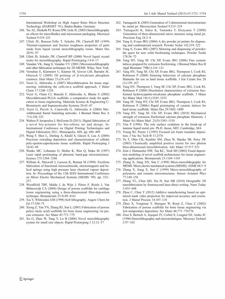
International Workshop on High Aspect Ratio Micro StructureTechnology (HARMST ‘01), Baden-Baden, Germany
246. Tse AL, Hesketh PJ, Rosen DW, Gole JL (2003) Stereolithographyon silicon for microfluidics and microsensor packaging. MicrosystTechnol 9:319–323
247. Ullett JS, Benson-Tolle T, Schultz JW, Chartoff RP (1999)Thermal-expansion and fracture toughness properties of partsmade from liquid crystal stereolithography resins. Mater Des20:91–97
248. Ullett JS, Schultz JW, Chartoff RP (2000) Novel liquid crystalresins for stereolithography. Rapid Prototyping J 6:8–17
249. Varadan VK, Jiang S, Varadan VV (2001) Microstereolithographyand other fabrication techniques for 3D MEMS. Wiley, New York
250. Vorndran E, Klammert U, Klarner M, Grover LM, Barralet JE,Gbureck U (2009) 3D printing of β-tricalcium phosphateceramics. Dent Mater 25:e18–e19
251. Vozzi G, Ahluwalia A (2007) Microfabrication for tissue engi-neering: rethinking the cells-on-a scaffold approach. J MaterChem 17:1248–1254
252. Vozzi G, Flaim CJ, Bianchi F, Ahluwalia A, Bhatia S (2002)Microfabricated PLGA scaffolds: a comparative study for appli-cation to tissue engineering. Materials Science & Engineering C-Biomimetic and Supramolecular Systems 20:43–47
253. Vozzi G, Previti A, Ciaravella G, Ahluwalia A (2004) Mic-rofabricated fractal branching networks. J Biomed Mater Res A71A:326–333
254. Walters P, Ieropoulos I, McGoran D (2011). Digital fabrication ofa novel bio-actuator for bio-robotic art and design. In:International Conference on Digital Printing Technologies andDigital Fabrication 2011, Minneapolis, MN. pp. 496–499
255. Wang F, Shor L, Darling A, Khalil S, Güceri S, Lau A (2004)Precision extruding deposition and characterization of cellularpoly-epsilon-caprolactone tissue scaffolds. Rapid Prototyping J10:42–49
256. Wanke MC, Lehmann O, Muller K, Wen Q, Stuke M (1997)Laser rapid prototyping of photonic band-gap microstructures.Science 275:1284–1286
257. William K, Maxwell J, Larsson K, Boman M (1999). Freeformfabrication of functional microsolenoids, electromagnets and he-lical springs using high pressure laser chemical vapour deposi-tion. In: Proceedings of the 12th IEEE International Conferenceon Micro Electro Mechanical Systems (MEMS ‘99). pp. 232–237.
258. Woodfield TBF, Malda J, de Wijn J, Péters F, Riesle J, VanBlitterswijk CA (2004) Design of porous scaffolds for cartilagetissue engineering using a three-dimensional fiber-depositiontechnique. Biomaterials 25:4149–4161
259. Xia Y, Whitesides GM (1998) Soft lithography. Angew Chem IntEd 37:550–75
260. Xiong Z, Yan YN, Zhang RJ, Sun L (2001) Fabrication of porouspoly(L-lactic acid) scaffolds for bone tissue engineering via pre-cise extrusion. Scr Mater 45:773–779
261. Xu G, Zhao W, Tang Y, Lu B (2006) Novel stereolithographysystem for small size objects. Rapid Prototyping J 12:12–17
262. Yamaguchi K (2003) Generation of 3-dimensional microstructureby metal jet. Microsystem Technol 9:215–219
263. Yamaguchi K, Sakai K, Yamanka T, Hirayama T (2000)Generation of three-dimensional micro structure using metal jet.Precision Eng 24:2–8
264. Yang S, Evans JRG (2004) A dry powder jet printer for dispens-ing and combinatorial research. Powder Techn 142:219–222
265. Yang S, Evans JRG (2007) Metering and dispensing of powder;the quest for new solid freeforming techniques. Powder Techn178:56–72
266. Yang HY, Yang SF, Chi XP, Evans JRG (2006) Fine ceramiclattices prepared by extrusion freeforming. J Biomed Mater Res BAppl Biomater 79B(1):116–121
267. Yang HY, Yang SF, Chi XP, Evans JRG, Thompson I, Cook RJ,Robinson P (2008) Sintering behaviour of calcium phosphatefilaments for use as hard tissue scaffolds. J Eur Ceram Soc 28(1):159–167
268. Yang HY, Thompson I, Yang SF, Chi XP, Evans JRG, Cook RJ,Robinson P (2008) Dissolution characteristics of extrusion free-formed hydroxyapatite-tricalcium phosphate scaffolds. J MaterSci Mater Med 19(11):3345–3353
269. Yang SF, Yang HY, Chi XP, Evans JRG, Thompson I, Cook RJ,Robinson P (2008c) Rapid prototyping of ceramic lattices forhard tissue scaffolds. Mater Des 29:1802–1809
270. Yang HY, Yang SF, Chi XP, Evans JRG (2010) Mechanicalstrength of extrusion freeformed calcium phosphate filaments. JMater Sci Mater Med 21(5):1503–1510
271. Yim P (1996). The role surface oxidation in the break-up oflaminar liquid metal jets. Ph.D. thesis, MIT, Cambridge, MA
272. Young RJ, Puretz J (1995) Focused ion beam insulator deposi-tion. J Vac Sci Tech B 13:2576
273. Yu T, Ober CK, Kuebler SM, Zhou W, Marder SR, Perry JW(2003) Chemically amplified positive resists for two photonthree-dimensional microfabrication. Adv Mater 15:517–521
274. Zein I, Hutmacher DW, Tan KC, Teoh SH (2002) Fused deposi-tion modeling of novel scaffold architectures for tissue engineer-ing applications. Biomaterials 23:1169–1185
275. Zhang X, Jiang XN, Sun C (1998) Micro-stereolithography forMEMS.Micro electro mechanical systems (MEMS). ASME 66:3–9
276. Zhang X, Jiang X, Sun C (1999) Micro-stereolithography ofpolymeric and ceramic microstructures. Sensor Actuator Phys77:149–156
277. Zhang YL, Chen QD, Xia H, Sun HB (2010) Designable 3Dnanofabrication by femtosecond laser direct writing. Nano Today5:435–448
278. Zhou C, Chen Y (2012) Additive manufacturing based on opti-mized mask video projection for improved accuracy and resolu-tion. J Manuf Process 14:107–118
279. Zhuo X, Yongnian Y, Shenguo W, Renji Z, Chao Z (2002)Fabrication of porous scaffolds for bone tissue engineering vialow-temperature deposition. Scr Mater 46:771–776776
280. Zissi S, Bertsch A, Jejequel JY, Corbel S, Lougnot DJ, Andre JC(1996) Stereolithography and microtechniques. Microsys Technol2:97–102
1754 Int J Adv Manuf Technol (2013) 67:1721–1754