frontiers of additive manufacturing research and...
TRANSCRIPT
Frontiers of Additive
Manufacturing Research and Education
An NSF Additive Manufacturing Workshop Report July 11 and 12,
2013
Yong Huang Ming C. Leu
March 2014

Frontiers of Additive Manufacturing Research and Education
Report of NSF Additive Manufacturing Workshop
July 11 and 12, 2013
Yong Huang
Department of Mechanical and Aerospace Engineering University of Florida Gainesville, FL 32611
Ming C. Leu
Department of Mechanical and Aerospace Engineering Missouri University of Science and Technology
Rolla, MO 65409
Published by
University of Florida Center for Manufacturing Innovation
PO Box 116250
Gainesville, FL 32611-6250 United States of America
March 2014

i
TABLE OF CONTENTS EXECUTIVE SUMMARY ii
1. INTRODUCTION 1 1.1 Background 1 1.2 Objective 2 1.3 Workshop overview 2
2. CURRENT STATE AND FUTURE POTENTIAL 3 2.1 Current state-of-the-art 3
2.1.1 Technology and research 3 2.1.1.1 Technology classification 3 2.1.1.2 Applications 6
2.1.2 University-industry collaboration and technology transfer 7 2.1.3 Education and training 8
2.1.3.1 Education and training for additive manufacturing 8 2.1.3.2 Additive manufacturing for education and training 9
2.2 Future Potential 10 2.2.1 Technology and research 10
2.2.1.1 Technology viewpoint 10 2.2.1.2 Economy and sustainability viewpoint 11
2.2.2 University-industry collaboration and technology transfer 11 2.2.3 Education and training 12
3. GAPS AND NEEDS 12 3.1 Technology and research 12
3.1.1 Materials 13 3.1.2 Design 13 3.1.3 Modeling, sensing, control, and process innovation 14 3.1.4 Characterization and certification 15 3.1.5 System integration and cyber implementation 16
3.2 University-industry collaboration and technology transfer 16 3.3 Education and training 17
4. RECOMMENDATIONS 18 4.1 Technology and research 18 4.2 University-industry collaboration and technology transfer 20 4.3 Education and training 21
4.3.1 University-community college partnership model 21 4.3.2 Teaching factory 21 4.3.3 Other education and training efforts 21
Appendix A (Organizers, discussion moderators, and invited speakers) 23 Appendix B (NSF Sponsoring Programs) 25
References Cited 26
ii
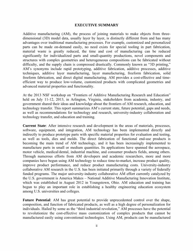
EXECUTIVE SUMMARY Additive manufacturing (AM), the process of joining materials to make objects from three-dimensional (3D) model data, usually layer by layer, is distinctly different from and has many advantages over traditional manufacturing processes. For example, customized and personalized parts can be made on-demand easily, no need exists for special tooling in part fabrication, material waste is greatly reduced, the time and cost of manufacturing can be reduced significantly for individualized parts and small-quantity productions, novel components and structures with complex geometries and heterogeneous compositions can be fabricated without difficulty, and the supply chain is compressed drastically. Commonly known as “3D printing,” AM’s synonyms include rapid prototyping, additive fabrication, additive processes, additive techniques, additive layer manufacturing, layer manufacturing, freeform fabrication, solid freeform fabrication, and direct digital manufacturing. AM provides a cost-effective and time-efficient way to produce low-volume, customized products with complicated geometries and advanced material properties and functionality. At the 2013 NSF workshop on “Frontiers of Additive Manufacturing Research and Education” held on July 11-12, 2013, in Arlington, Virginia, stakeholders from academia, industry, and government shared their ideas and knowledge about the frontiers of AM research, education, and technology transfer. This report summarizes AM’s current state, future potential, gaps and needs, as well as recommendations for technology and research, university-industry collaboration and technology transfer, and education and training. Current State: After intensive research and development in the areas of materials, processes, software, equipment, and integration, AM technology has been implemented directly and indirectly to produce prototype parts with specific material properties for evaluation and testing, as well as tools, dies and molds. The direct fabrication of functional end-use products is becoming the main trend of AM technology, and it has been increasingly implemented to manufacture parts in small or medium quantities. Its applications have spanned the aerospace, motor vehicle, medical/dental, industrial machine, and consumer products fields, among others. Through numerous efforts from AM developers and academic researchers, more and more companies have begun using AM technology to reduce time-to-market, increase product quality, improve product performance, and reduce product manufacturing costs. University-industry collaborative AM research in the U.S. has been initiated primarily through a variety of federally funded programs. The major university-industry collaborative AM effort currently catalyzed by the U.S. government is America Makes – National Additive Manufacturing Innovation Institute, which was established in August 2012 in Youngstown, Ohio. AM education and training has begun to play an important role in establishing a healthy engineering education ecosystem among U.S. universities and colleges. Future Potential: AM has great potential to provide unprecedented control over the shape, composition, and function of fabricated products, as well as a high degree of personalization for individuals. Hailed by some as the “third industrial revolution,” AM processes have the potential to revolutionize the cost-effective mass customization of complex products that cannot be manufactured easily using conventional technologies. Using AM, products can be manufactured
iii
with a broad range of sizes, materials, and functionalities. Future applications may include conformal, flexible electronics; products with embedded multi-material sensors and actuators; high-power, high-energy-density microbatteries; cellular machines; turbine blades with internal cavities; lightweight, high-strength aerospace structures with material gradients; multi-functional houses; custom medications; and even human organs, to name a few. In general, AM enables the printing of complex shapes with controllable compositions and active functions. In terms of economy and sustainability, AM offers multiple advantages over conventional manufacturing technologies, including reduced material waste and energy consumption, shortened time-to-market, just-in-time production, and fabrication of structures not possible by traditional means. From the education and training perspective, AM holds the potential to promote science, technology, engineering, and mathematics (STEM) education because it can engage a broad population – both students and adults – in both formal and informal settings. Gaps and Needs: While AM processes have advanced greatly in recent years, many challenges remain to be addressed, such as limited materials available for use in AM processes, relatively poor part accuracy caused by the stair-stepping effect, insufficient repeatability and consistency of the produced parts, and lack of in-process qualification and certification methodologies. In order to realize AM’s potential to usher in the “third industrial revolution,” the products must be fabricated rapidly, efficiently, and inexpensively while meeting all stringent functional requirements. Many research efforts are needed to expedite the transformation from rapid prototyping to additive manufacture of advanced materials that boast material flexibility, the ability to generate fine features, and high throughput. University-industry collaboration in AM must consider business opportunities. Mass customization is an AM business frontier, the key to which is the capability of 3D printing of a vast array of components from heterogeneous materials. Mass production could potentially be another business frontier. To compete with conventional mass production processes, AM technology needs to advance significantly in order to drastically reduce the cost of production, improve the performance of fabricated parts, and achieve consistency between parts. While numerous AM educational resources and training materials currently exist, no readily applicable, proven model for AM education and training is available. Recommendations: Based on the identified technology gaps and research needs, we have summarized our recommendations for AM technology and research in terms of materials, design, modeling, sensing and control, process innovation, and system integration. There is a tight coupling among material development, process development, process sensing and control, and the qualification and certification of products fabricated by AM. As in the progression of many other emerging technologies, the greatest advancements will come at the boundaries of fundamental material science, physics, biology, lasers, electronics, optics, metrology, and control. To provide the technological breakthroughs required to establish the new “certify-as-you-build” manufacturing paradigm, fundamental research and advanced development will be needed in order to handle the in situ diagnostics and control of AM processes by integrating modeling, sensing, and process control. For university-industry collaboration and technology transfer, our recommendations include incentivizing projects through federal funding, increasing federal research and development support, and increasing coordination efforts for public-private partnerships. For education and training, we recommend a university-community college

iv
partnership model with resource sharing and a teaching factory model to expose students directly to manufacturing enterprises. In addition, we recommend promoting the public awareness of AM, using the Internet to drastically increase outreach and resource sharing, and establishing publicly accessible AM facilities.
1
1. INTRODUCTION 1.1 Background
The ASTM International Committee F42 on Additive Manufacturing (AM) Technologies defines AM as the “process of joining materials to make objects from three-dimensional (3D) model data, usually layer by layer, as opposed to subtractive manufacturing methodologies [1].” Any AM process is distinctly different from traditional manufacturing processes such as machining, casting, forming, etc. Commonly known as “3D printing,” AM is a suite of computer-automated processes that fabricates physical 3D objects layer by layer from Computer-Aided Design (CAD) models using metallic, plastic, ceramic, composite, and biological materials. The many advantages of this technology over other manufacturing processes include the following: parts can be made easily on-demand for customization and personalization, no need exists for special tooling in part fabrication, material waste is greatly reduced, the time and cost of manufacturing can be reduced significantly for individualized parts and small-quantity productions, novel components and structures of complex geometries and heterogeneous compositions can be fabricated without difficulty, and the supply chain is compressed drastically. AM’s synonyms include rapid prototyping, additive fabrication, additive processes, additive techniques, additive layer manufacturing, layer manufacturing, freeform fabrication, solid freeform fabrication, and direct digital manufacturing. Since its inception in the mid-1980s, AM has evolved and blossomed into a plethora of processes, including Stereolithography (SLA), Fused Deposition Modeling (FDM), 3D Printing (3DP), Laminated Object Manufacturing (LOM), Selective Laser Sintering (SLS), Selective Laser Melting (SLM), Laser Metal Deposition (LMD), inkjet printing, and others. As AM becomes a transforming technology, its impact continues to grow in terms of the total number of fabricated parts, number of new start-up companies, funding opportunities, number of publications and patents, and public awareness. A series of previous events and reports provide a historical context of AM progress. A World Technology Evaluation Center (WTEC) study on rapid prototyping in Europe and Japan was performed in 1996 [2]. Two years later, a roadmap study on rapid prototyping sponsored by the National Center for Manufacturing Sciences was completed [3]. A second WTEC study was conducted in 2003 to assess the level of activity in Europe pertaining to additive/subtractive technologies [4]. In 2009, the National Science Foundation (NSF) and the Office of Naval Research (ONR) sponsored the Roadmap for Additive Manufacturing (RAM) Workshop; its primary objectives were to define and focus research activity in the area of AM with the intent of accelerating the technology’s commercial acceptance, to increase the impact and significance of AM research, and to articulate a roadmap for research in this field for the next 10-12 years [5]. Recent innovations in materials and processes are transforming 3D printing from rapid prototyping to rapid manufacturing. This allows manufacturing near the point of use, enabling “on-demand” manufacturing and drastically reducing inventories and wait times. This has contributed greatly to the fast growth of the AM market since its beginning in 1988. According to the 2013 Wohlers Report [6], the compound annual growth rate of worldwide revenues of all AM products and services over the past 25 years was 25.4%. The rate of growth was 27.4% over the three-year period from 2010 to 2012, reaching $2.2 billion in 2012. The unit sales of
2
industrial AM systems (unit price > $5,000) increased by 19.3% to 7,771 units in 2012, while the unit sales of 3D personal printers (unit price ≤ $5,000) increased by 46.3% to 35,508 units in the same year. The U.S. has been the world leader in terms of the number of industrial AM systems installed. AM spurs innovation because it can be used to manufacture many designs of complex geometries quickly and without difficulty. Thus, it is popularly touted as a technology that can make anything. By eliminating many constraints imposed by conventional manufacturing, AM may bring about a paradigm shift from Design for Manufacturing (DFM) to Manufacturing for Design (MFD). This paradigm shift will create increased application and market opportunities for AM. One such opportunity could be the integration of AM with 3D imaging to create 3D Fax Technology, in which the sender scans a 3D object in cross-sections and sends out the digital image in layers, and then the recipient receives the layered image and uses an AM machine to fabricate the 3D object. 1.2 Objective
The objective of the NSF workshop on “Frontiers of Additive Manufacturing Research and Education” was to provide a forum for sharing ideas and disseminating information about the frontiers of AM research, education, and technology transfer. The workshop participants discussed the current state-of-the-art and future potential of AM, analyzed the gaps between the future potential and the present reality, and identified what needs to be done in the areas of research, education, and technology transfer in order to close the gaps. An extensive research roadmap was developed at the NSF/ONR Roadmap for Additive Manufacturing (RAM) Workshop in 2009, so the present workshop was not intended to develop another roadmap; rather, the goal was to provide a forum for the workshop participants to learn about the frontiers of AM research, education, and technology transfer and to share their ideas and thoughts about these different but interconnected aspects. The workshop was attended primarily by researchers and educators interested in engaging in AM research and education, industrialists interested in the transfer of AM technology through university-industry collaboration, and administrators and decision makers who support and facilitate these activities. 1.3 Workshop overview
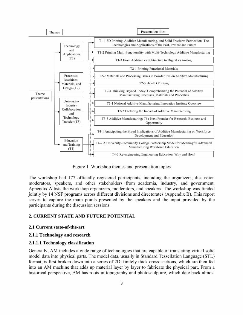
This two-day workshop was held on July 11-12, 2013, in Arlington, Virginia. It covered the following four themes: 1) technology and applications, 2) processes, machines, materials, and design, 3) university-industry collaboration and technology transfer, and 4) education and training. Each theme was organized as a half-day session consisting of three or four plenary presentations, as shown in Figure 1. Each presentation was given by an expert in a specific AM area, and each session was followed by a plenary discussion in which the participants asked questions to the speakers, shared their knowledge and ideas about AM, and discussed the gaps that must be filled through research, education, and technology transfer, as well as the actions required to close the gaps.
3
Theme presentations
Processes, Machines,
Materials, and Design (T2)
Technology and
Applications (T1)
T1-1 3D Printing, Additive Manufacturing, and Solid Freeform Fabrication: The Technologies and Applications of the Past, Present and Future
T1-2 Printing Multi-Functionality with Multi-Technology Additive Manufacturing
T2-1 Printing Functional Materials
T2-2 Materials and Processing Issues in Powder Fusion Additive Manufacturing
T2-3 Bio-3D Printing
Presentation titlesThemes
T1-3 From Additive vs Subtractive to Digital vs Analog
University-Industry
Collaboration and
Technology Transfer (T3)
T3-2 Factoring the Impact of Additive Manufacturing
T3-3 Additive Manufacturing: The Next Frontier for Research, Business and Opportunity
T3-1 National Additive Manufacturing Innovation Institute Overview
Education and Training
(T4)
T4-1 Anticipating the Broad Implications of Additive Manufacturing on Workforce Development and Education
T4-2 A University-Community College Partnership Model for Meaningful Advanced Manufacturing Workforce Education
T4-3 Re-engineering Engineering Education: Why and How!
T2-4 Thinking Beyond Today: Comprehending the Potential of Additive Manufacturing Processes, Materials and Properties
Figure 1. Workshop themes and presentation topics The workshop had 177 officially registered participants, including the organizers, discussion moderators, speakers, and other stakeholders from academia, industry, and government. Appendix A lists the workshop organizers, moderators, and speakers. The workshop was funded jointly by 14 NSF programs across different divisions and directorates (Appendix B). This report serves to capture the main points presented by the speakers and the input provided by the participants during the discussion sessions. 2. CURRENT STATE AND FUTURE POTENTIAL 2.1 Current state-of-the-art
2.1.1 Technology and research
2.1.1.1 Technology classification
Generally, AM includes a wide range of technologies that are capable of translating virtual solid model data into physical parts. The model data, usually in Standard Tessellation Language (STL) format, is first broken down into a series of 2D, finitely thick cross-sections, which are then fed into an AM machine that adds up material layer by layer to fabricate the physical part. From a historical perspective, AM has roots in topography and photosculpture, which date back almost

4
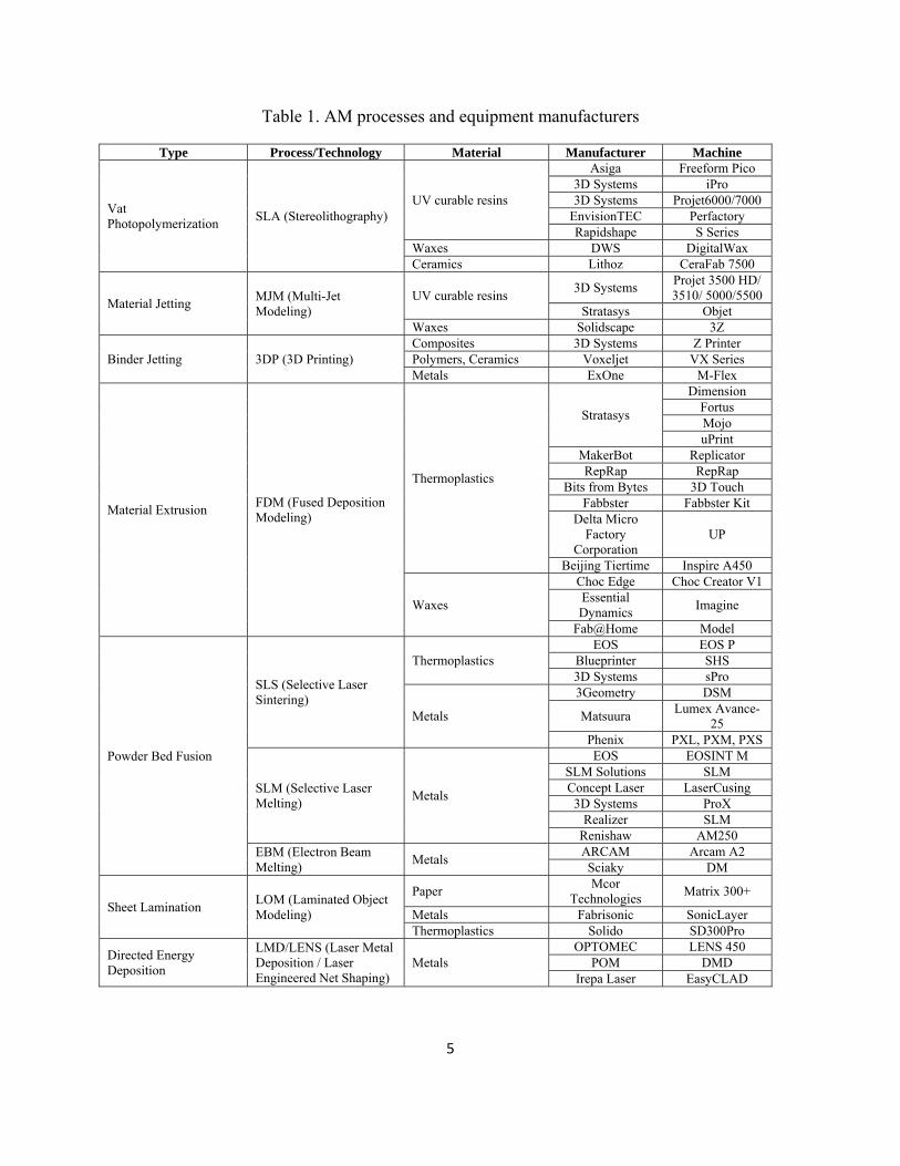
150 years; both can be viewed as manual “cut and stack” approaches to building a freeform object in a layer-wise fashion. The first successful AM process, proposed by Ciraud in 1972, was essentially a powder deposition method using an energy beam [7]. After intensive research and development in the areas of materials, processes, software, equipment, and integration, AM has been used directly and indirectly to produce prototype parts with suitable material properties for evaluation and testing, as well as to make tools, dies, and molds. Currently, the direct fabrication of functional end-use products is becoming the main trend of AM technology, and it has been increasingly implemented to manufacture parts in small or medium quantities. According to the ASTM F42 committee, AM processes are classified into seven categories [1], as listed in Table 1. These processes differ from each other in terms of the techniques used to deposit layers and the ways in which the deposited layers are bonded together. Table 1 provides information about the process variations, materials covered by each process, commercial manufacturers, and machine models for each of the seven categories. For each technology, even the same manufacturer may have different machine models that vary from each other in terms of the build envelope, fabrication speed, layer thickness, droplet diameter, range of materials, accuracy, and/or cost. There are different ways to categorize AM processes. For example, one approach is to classify them into four broad categories based on whether the starting materials exist as a liquid, filament/paste, powder, or solid sheet [8, 9]. AM processes also may be categorized based on the types of part materials, such as polymers, metals, ceramics, composites, and biological materials.
5
Table 1. AM processes and equipment manufacturers
Type Process/Technology Material Manufacturer Machine
Vat Photopolymerization
SLA (Stereolithography) UV curable resins
Asiga Freeform Pico 3D Systems iPro 3D Systems Projet6000/7000
EnvisionTEC Perfactory Rapidshape S Series
Waxes DWS DigitalWax Ceramics Lithoz CeraFab 7500
Material Jetting MJM (Multi-Jet Modeling)
UV curable resins 3D Systems
Projet 3500 HD/ 3510/ 5000/5500
Stratasys Objet Waxes Solidscape 3Z
Binder Jetting 3DP (3D Printing) Composites 3D Systems Z Printer Polymers, Ceramics Voxeljet VX Series Metals ExOne M-Flex
Material Extrusion FDM (Fused Deposition Modeling)
Thermoplastics
Stratasys
Dimension Fortus Mojo uPrint
MakerBot Replicator RepRap RepRap
Bits from Bytes 3D Touch Fabbster Fabbster Kit
Delta Micro Factory
Corporation UP
Beijing Tiertime Inspire A450
Waxes
Choc Edge Choc Creator V1 Essential Dynamics
Imagine
Fab@Home Model
Powder Bed Fusion
SLS (Selective Laser Sintering)
Thermoplastics EOS EOS P
Blueprinter SHS 3D Systems sPro
Metals
3Geometry DSM
Matsuura Lumex Avance-
25 Phenix PXL, PXM, PXS
SLM (Selective Laser Melting)
Metals
EOS EOSINT M SLM Solutions SLM Concept Laser LaserCusing 3D Systems ProX
Realizer SLM Renishaw AM250
EBM (Electron Beam Melting)
Metals ARCAM Arcam A2 Sciaky DM
Sheet Lamination LOM (Laminated Object Modeling)
Paper Mcor
Technologies Matrix 300+
Metals Fabrisonic SonicLayer Thermoplastics Solido SD300Pro
Directed Energy Deposition
LMD/LENS (Laser Metal Deposition / Laser Engineered Net Shaping)
Metals OPTOMEC LENS 450
POM DMD Irepa Laser EasyCLAD
6
2.1.1.2 Applications
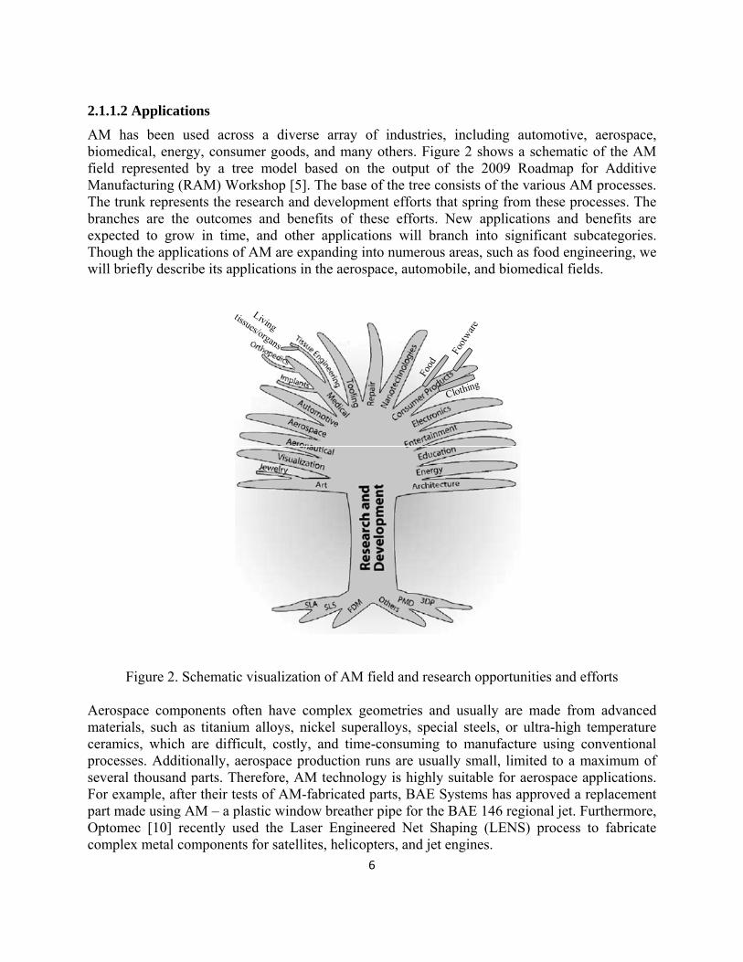
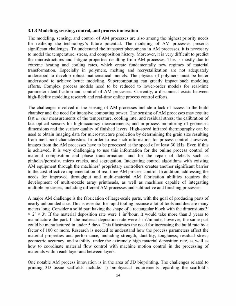
AM has been used across a diverse array of industries, including automotive, aerospace, biomedical, energy, consumer goods, and many others. Figure 2 shows a schematic of the AM field represented by a tree model based on the output of the 2009 Roadmap for Additive Manufacturing (RAM) Workshop [5]. The base of the tree consists of the various AM processes. The trunk represents the research and development efforts that spring from these processes. The branches are the outcomes and benefits of these efforts. New applications and benefits are expected to grow in time, and other applications will branch into significant subcategories. Though the applications of AM are expanding into numerous areas, such as food engineering, we will briefly describe its applications in the aerospace, automobile, and biomedical fields.
Figure 2. Schematic visualization of AM field and research opportunities and efforts
Aerospace components often have complex geometries and usually are made from advanced materials, such as titanium alloys, nickel superalloys, special steels, or ultra-high temperature ceramics, which are difficult, costly, and time-consuming to manufacture using conventional processes. Additionally, aerospace production runs are usually small, limited to a maximum of several thousand parts. Therefore, AM technology is highly suitable for aerospace applications. For example, after their tests of AM-fabricated parts, BAE Systems has approved a replacement part made using AM – a plastic window breather pipe for the BAE 146 regional jet. Furthermore, Optomec [10] recently used the Laser Engineered Net Shaping (LENS) process to fabricate complex metal components for satellites, helicopters, and jet engines.
7
In the automotive industry, AM technology has been explored as a tool in the design and development of automotive components because it can shorten the development cycle and reduce manufacturing and product costs. AM processes also have been used to make small quantities of structural and functional components, such as engine exhausts, drive shafts, gear box components, and braking systems for luxury, low-volume vehicles. Unlike passenger cars, vehicles for motorsports usually use lightweight alloys (e.g., titanium) and have highly complex structures and low production volumes. Companies and research institutes also have successfully applied AM techniques to manufacture functional components for racing vehicles. Ample AM application opportunities exist in the biomedical field for the fabrication of custom-shaped orthopedic prostheses and implants, medical devices, biological chips, tissue scaffolds, living constructs, drug-screening models, and surgical planning and training apparatuses. The year 2013 marked the 15th year of cell printing, an ambitious vision to create a developmental biology-enabled, scaffold-less technique to fabricate living tissues and organs by printing living cells [11, 12]. A typical cell printing process consists of three stages: 1) pre-processing: creating tissue- or organ-specific CAD models for each patient using CT scan data, 2) processing: using AM processes to deposit living cells into 3D biological constructs [12-14], and 3) post-processing: incubating printed tissues or organs to encourage tissue fusion and maturation. In industry, medium and large quantities of polymer-based components usually are manufactured by injection molding. It is difficult for AM to compete with injection molding in producing these components directly. However, AM processes can be used to manufacture the injection molds (called rapid tooling) to reduce the time and cost of new tool development. Similarly, metallic parts can also be casted from molds or dies made using AM technology. 2.1.2 University-industry collaboration and technology transfer
Through numerous efforts from AM developers and academic researchers, more and more companies have begun using AM technology to reduce time-to-market, increase product quality, improve product performance, and reduce product manufacturing costs. While AM processes have been widely adopted to fabricate polymeric parts, metal-based AM processes have recently emerged in industrial applications for manufacturing items such as automotive engines, aircraft assemblies, power tools, and manufacturing tools including jigs, fixtures, and drill guides [15]. Various AM processes have been introduced to the commercial market by industrial companies, including Electro Optical Systems (EOS) in Germany, Arcam in Sweden, MCP Tooling Technologies in the U.K., and Stratasys, 3D Systems, and Optomec in the U.S., among others. Collaborative university-industry research in AM in the U.S. has been initiated primarily through a variety of federally funded programs, such as the Small Business Innovation Research / Small Business Technology Transfer (SBIR/STTR) programs of most federal agencies, NSF’s Grant Opportunities for Academic Liaison with Industry (GOALI) and Industry/University Cooperative Research Centers (I/UCRC) programs, and various broad agency announcements of several federal agencies. Several non-federally funded industrial consortia also exist, such as the Center for Aerospace Manufacturing Technologies (CAMT) at the Missouri University of Science and Technology and the W. M. Keck Center for 3D Innovation at the University of Texas at El Paso. The major university-industry collaboration in AM currently supported by the
8
U.S. government is America Makes – National Additive Manufacturing Innovation Institute, which was established in August 2012 in Youngstown, Ohio. 2.1.3 Education and training
2.1.3.1 Education and training for additive manufacturing
Educating the general public about AM empowers people to build what they dream. Also, disseminating this technology to its many potential users will democratize manufacturing and spur innovation. Formal AM education has already been integrated into curricula at different levels. Educational materials on rapid prototyping have long been a part of manufacturing engineering courses at many engineering colleges, and some classical manufacturing textbooks, such as Manufacturing Processes for Engineering Materials by Kalpakjian and Schmid [16], have already included information on rapid prototyping, the precedent of AM. In addition, some AM-specific courses have been offered at both the undergraduate and graduate levels, such as the Solid Freeform Fabrication (ME 397/379M) course at the University of Texas at Austin and the Rapid Prototyping in Engineering (ME 7227) course at the Georgia Institute of Technology in Atlanta. Interestingly, community colleges have served as an excellent gateway for exposing students to AM techniques, and their courses tend to adapt to recent trends. Through the Advanced Technological Education (ATE) initiatives aimed at two-year colleges, NSF is promoting and supporting curricula through its Technician Education in Additive Manufacturing (TEAM) program. As part of this work, two ATE centers – MateEd at Edmonds Community College (Lynnwood, WA) and RapidTech at Saddleback College (Viejo, CA), which is housed at the University of California, Irvine – are pioneering the development of core competencies and curricula that can serve as models for expansion. To date, few educational institutions have developed or even have access to books, instructional guides, and other educational materials needed for courses and lab activities in AM [17]. Furthermore, the California Network for Manufacturing Innovation™, Inc. (CNMI) was established in early 2013 to create a flexible technician education framework, which draws on the experience of RapidTech to prepare the nation’s technical workforce for future technical occupations in advanced manufacturing. In addition, California launched the Advanced Manufacturing Project for Learning in Focused Innovation (AMPLiFI) program to develop technician education modules in advanced manufacturing suitable for infusion into the existing technical education coursework and to verify the efficacy of the framework through the development of support for focus-group workshops to promote open dialog regarding implementation at the community college level. AM education primarily has occurred at the level of higher education, i.e., among U.S. universities and colleges. However, one recent initiative at the secondary education level is the Defense Advanced Research Projects Agency (DARPA) Manufacturing Experimentation and Outreach (MENTOR) program, which provides 3D printers to 1,000 high schools. The MENTOR effort, part of the DARPA’s Adaptive Vehicle Make program portfolio, engages high school students in a series of collaborative, distributed manufacturing and design experiments. The overarching objective of MENTOR is to develop and motivate the next generation of system
9
designers and manufacturing innovators by exposing them to the principles of foundry-style digital manufacturing through modern prize-based design challenges. The development of a curriculum that exposes high school students to design concepts and collaboration is also part of the program. The program is still in its initial phases but is planned to be fully rolled out over the next four years. In the age of the Internet, various online resources have provided enormous complementary AM education and training to reach a much broader population [18]. The most notable of these is Makerspaces [18], community centers with tools that combine manufacturing equipment, community, and education for the purpose of enabling community members to design, prototype, and create manufactured works. Makerspaces represent the democratization of design, engineering, fabrication, and education. Though this is a fairly new phenomenon, their users already are beginning to produce projects with significant national impact. One of the Makerspace program’s goals is to find low-cost options for branching into more communities in places such as middle schools, community centers, and high schools. It is expected that such an effort will encourage the integration of online design and collaboration tools with low-cost options for physical workspaces where students and the general public alike may access educational support to gain practical, hands-on experience. Some AM-specific textbooks also have been produced by AM researchers, such as Additive Manufacturing Technologies: Rapid Prototyping to Direct Digital Manufacturing [19]. The book provides a comprehensive overview of AM technologies and descriptions of support technologies, such as software systems and post-processing approaches; discusses a wide variety of new and emerging applications, such as micro-scale AM, medical applications, direct write electronics, and direct digital manufacturing of end-use components; and introduces systematic solutions for AM process selection and design. 2.1.3.2 Additive manufacturing for education and training
In addition to education and training to learn about AM, this technology is taking an important role in establishing a healthy engineering education eco-system; in other words, AM is being used for education and training. For example, AM technologies have been widely implemented by FIRST Robotics teams because they provide a unique way to make robot parts and machines. Due to its freeform fabrication nature, AM products help students to comprehend complex, difficult-to-understand topics such as chemical and biological phenomena. For instance, the Center for BioMolecular Modeling of the Milwaukee School of Engineering (Milwaukee, WI) has applied AM to create physical models of protein and molecular structures. This creates innovative instructional materials that students can hold in their hands, thus making the molecular world real for them [20]. Human scaffolds and tissue models produced by AM can be used for surgical planning/training and drug screening modeling, respectively. Such examples demonstrate how AM can raise design education to a new level through the immediate recognition of a physical model.
10
2.2 Future Potential
2.2.1 Technology and research
2.2.1.1 Technology viewpoint
Technologically, AM provides unprecedented control over the shape, composition, and function of fabricated products, as well as a high degree of personalization for individuals. Hailed by some as the “third industrial revolution” [21], AM processes have the potential to revolutionize the cost-effective mass customization of complex products that cannot be manufactured easily using conventional technologies. Using AM, products can be manufactured with a broad range of sizes (from nanometer/micrometer scales to tens of meters), materials (metals, polymers, ceramics, composites, and biological materials), and functionalities (e.g., load-carrying brackets, energy conversion structures, and tissue-growing scaffolds). Its applications include conformal, flexible electronics; products with embedded, multi-material sensors and actuators; high-power, high-energy-density microbatteries; cellular machines; turbine blades with internal cavities; lightweight, high-strength aerospace structures with material gradients; multi-functional houses; custom medications; and even human organs, to name a few. In general, AM enables the printing of complex shapes with controllable compositions and active functions. Producing parts with functionally graded materials (FGM) can be uniquely enabled by AM. Some AM processes can deliver different materials to the building areas (usually through multiple feeding units) and have the ability to build components with FGM, which is one of the primary advantages of AM technology that cannot be realized by conventional manufacturing methods. This ability offers the flexibility to control the composition in order to provide multi-functionality (e.g., grading materials from tungsten carbide to enhance erosion resistance to cobalt for higher ductility) and to optimize the properties of the built part. One example application is a pulley that contains more carbide near the hub and rim to make it harder and more wear resistant, and less carbide in other areas to increase compliance [22]. Another example application is a missile nose cone with an ultra-high-temperature ceramic graded to a refractory metal from the cone’s outside to inside surface in order to sustain extreme external temperatures while attaching more easily to the metallic missile nose [9]. AM technology also enables printing functions through the programming of the behavior of active materials. This allows the manufactured part to function in several ways — to sense and react, to compute and behave; the ability to manufacture arbitrary active systems comprising both passive and active substructures will open the door to a new design space. In the biomedical field, AM can be used to fabricate tissue scaffolds that are biocompatible, biodegradable, and bioabsorbable as well as in vitro biological constructs with living cells and biological compounds. AM will not replace conventional manufacturing methods in the foreseeable future, especially for the high-volume production of parts with low complexity and high accuracy. However, AM may still bring revolutionary advances to the manufacturing industry through its integration with conventional manufacturing technologies. For example, laser metal deposition has been integrated with CNC machining as a hybrid process [23]. For high-volume production, AM may
11
also provide technological support, such as through the fabrication and repair of dies and molds used by other manufacturing processes, such as injection molding. 2.2.1.2 Economy and sustainability viewpoint
In terms of economy and sustainability, AM offers multiple advantages over conventional manufacturing techniques, including reduced material waste and energy consumption, shortened time-to-market, just-in-time production, and fabrication of structures not possible traditionally. In particular, adding materials layer by layer to create 3D objects greatly reduces waste materials. In traditional aerospace manufacturing, for example, titanium parts are machined down to size from large titanium blocks, which may generate up to 90% in waste material that cannot be reused readily. AM could greatly reduce such waste generation, thus reducing the energy required to produce titanium material and parts from titanium [15]. Moreover, the digital nature of AM will enable manufacturers to adapt new product designs without the additional expenses of new physical tools associated with conventional processes. 2.2.2 University-industry collaboration and technology transfer
To increase U.S. manufacturing competitiveness and regain world leadership in manufacturing, President Obama’s administration has been developing and implementing new mechanisms and making game-changing investments to better allow U.S. manufacturers to produce goods in the U.S. and sell them everywhere. The National Network for Manufacturing Innovation (NNMI), which President Obama announced in March 2012, is a major initiative to accelerate innovation and increase U.S. manufacturing competitiveness by bringing together federal agencies, industry, universities and community colleges, and state governments to invest in industrially relevant manufacturing technologies with broad applications. America Makes – National Additive Manufacturing Innovation Institute (NAMII) was created in August 2012 as the NNMI pilot institute. This successful public-private partnership has brought together many universities, research organizations, and industry partners from across the nation, with over $45 million in federal investment and an even larger amount of matching dollars from other sources. It represents a high-level partnership in manufacturing technology across industry, government, and academia. The Technology Readiness Level (TRL) / Manufacturing Readiness Level (MRL) addressed by America Makes is 4-7, which is aimed at bridging the gap in manufacturing innovation between research done by universities and government laboratories and commercialization done by the private sector. The efforts of America Makes include technology development, technology transition, workforce/educational outreach, and advanced manufacturing enterprises. America Makes had over 90 organizations across the U.S. joining as its members as of January 2014. Many government-driven AM initiatives are growing outside the United States [24]. For example, in 2013, the government of Singapore announced its plans to invest $403 million over five years in advanced manufacturing, including 3D printing; the central government of China declared its readiness to invest approximately $240 million in AM research, development, and commercialization; and the European Union and other countries in Europe have been funding more and more AM projects. The European Space Agency recently initiated a 4.5-year program entitled “Additive Manufacturing Aiming Towards Zero Waste and Efficient Production of High-Tech Metal Products.”
12
2.2.3 Education and training
AM holds great potential for promoting science, technology, engineering, and mathematics (STEM) education because it can engage a broad population – both students and adults – in both formal and informal settings. The availability of low-cost 3D printing equipment is creating the opportunity for AM-enabled, hands-on labs in primary, secondary, and postsecondary schools across the nation. These programs involve not only traditional engineering but also the biological sciences (molecular modeling), medicine (orthopedic implants and tissue engineering), fashion design (clothing, footwear, and jewelry), sports science (protective gear), law enforcement and forensics (recreation of crime scenes), archaeology (bones and artifacts), interior design (space and facilities planning), and architecture (scaled models) [17]. Also, AM presents a great opportunity to revitalize manufacturing programs at U.S. universities through a new curriculum in advanced product development. The continued reduction in the prices of desktop AM machines will create an opportunity to produce 3D printers suitable for use by children. A prototype AM machine, to be priced at around $800, is being designed by Origo, a European company. XYZprinting Inc. of Taiwan recently announced a new personal 3D printer priced at $500. Similar to the way in which a Makerspace gives adults a space to tinker and experiment with STEM concepts, a personal 3D printer at home could offer children the same opportunity to explore their ideas and to learn through hands-on experiences [17]. 3. GAPS AND NEEDS 3.1 Technology and research
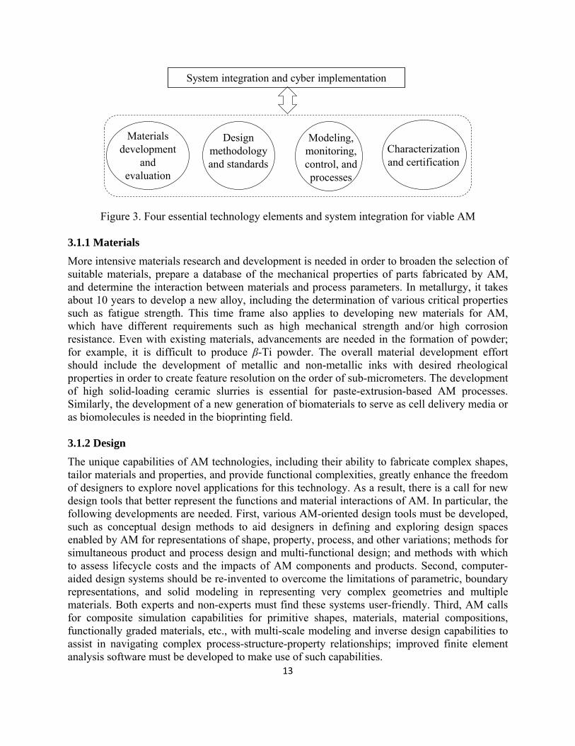
While AM techniques have progressed greatly in recent years, many challenges remain to be addressed, such as limited materials available for use in AM processes, relatively poor part accuracy caused by the stair-stepping effect, insufficient repeatability and consistency in the produced parts, and lack of qualification and certification methodologies for AM processes. In order to realize the AM-enabled “third industrial revolution,” the products must be fabricated rapidly, efficiently, and inexpensively while meeting all stringent functional requirements. Research is needed to expedite the transformation of 3D printing from rapid prototyping to the additive manufacture of advanced materials that boast material flexibility, the ability to generate fine features (< 100 microns), and high throughput. In particular, the four AM technology elements and system integration shown in Figure 3 are addressed in the following subsections in terms of gaps and needs, based on the views of the expert presenters and other workshop attendees who participated in the discussion sessions.
13
Materials development
and evaluation
System integration and cyber implementation
Design methodology and standards
Modeling, monitoring, control, and processes
Characterization and certification
Figure 3. Four essential technology elements and system integration for viable AM 3.1.1 Materials
More intensive materials research and development is needed in order to broaden the selection of suitable materials, prepare a database of the mechanical properties of parts fabricated by AM, and determine the interaction between materials and process parameters. In metallurgy, it takes about 10 years to develop a new alloy, including the determination of various critical properties such as fatigue strength. This time frame also applies to developing new materials for AM, which have different requirements such as high mechanical strength and/or high corrosion resistance. Even with existing materials, advancements are needed in the formation of powder; for example, it is difficult to produce β-Ti powder. The overall material development effort should include the development of metallic and non-metallic inks with desired rheological properties in order to create feature resolution on the order of sub-micrometers. The development of high solid-loading ceramic slurries is essential for paste-extrusion-based AM processes. Similarly, the development of a new generation of biomaterials to serve as cell delivery media or as biomolecules is needed in the bioprinting field. 3.1.2 Design
The unique capabilities of AM technologies, including their ability to fabricate complex shapes, tailor materials and properties, and provide functional complexities, greatly enhance the freedom of designers to explore novel applications for this technology. As a result, there is a call for new design tools that better represent the functions and material interactions of AM. In particular, the following developments are needed. First, various AM-oriented design tools must be developed, such as conceptual design methods to aid designers in defining and exploring design spaces enabled by AM for representations of shape, property, process, and other variations; methods for simultaneous product and process design and multi-functional design; and methods with which to assess lifecycle costs and the impacts of AM components and products. Second, computer-aided design systems should be re-invented to overcome the limitations of parametric, boundary representations, and solid modeling in representing very complex geometries and multiple materials. Both experts and non-experts must find these systems user-friendly. Third, AM calls for composite simulation capabilities for primitive shapes, materials, material compositions, functionally graded materials, etc., with multi-scale modeling and inverse design capabilities to assist in navigating complex process-structure-property relationships; improved finite element analysis software must be developed to make use of such capabilities.
14
3.1.3 Modeling, sensing, control, and process innovation
The modeling, sensing, and control of AM processes are also among the highest priority needs for realizing the technology’s future potential. The modeling of AM processes presents significant challenges. To understand the transport phenomena in AM processes, it is necessary to model the temperature, stress, and composition history. Moreover, it is very difficult to predict the microstructures and fatigue properties resulting from AM processes. This is mostly due to extreme heating and cooling rates, which create fundamentally new regimes of material transformation. Especially in polymers, melting and recrystallization are not adequately understood to develop robust mathematical models. The physics of polymers must be better understood to achieve better modeling. Supercomputing can greatly impact such modeling efforts. Complex process models need to be reduced to lower-order models for real-time parameter identification and control of AM processes. Currently, a disconnect exists between high-fidelity modeling research and real-time online process control efforts. The challenges involved in the sensing of AM processes include a lack of access to the build chamber and the need for intensive computing power. The sensing of AM processes may require fast in situ measurements of the temperature, cooling rate, and residual stress; the calibration of fast optical sensors for high-accuracy measurements; and in-process monitoring of geometric dimensions and the surface quality of finished layers. High-speed infrared thermography can be used to obtain imaging data for microstructure prediction by determining the grain size resulting from melt pool characteristics. In order to use such information for process control, however, images from the AM processes have to be processed at the speed of at least 30 kHz. Even if this is achieved, it is very challenging to use this information for the online process control of material composition and phase transformation, and for the repair of defects such as pinholes/porosity, micro cracks, and segregation. Integrating control algorithms with existing AM equipment through the machines’ proprietary controllers creates another significant barrier to the cost-effective implementation of real-time AM process control. In addition, addressing the needs for improved throughput and multi-material AM fabrication abilities requires the development of multi-nozzle array printheads, as well as machines capable of integrating multiple processes, including different AM processes and subtractive and finishing processes. A major AM challenge is the fabrication of large-scale parts, with the goal of producing parts of nearly unbounded size. This is essential for rapid tooling because a lot of tools and dies are many meters long. Consider a solid part having the shape of a rectangular block with the dimensions 3′ × 2′ × 3′. If the material deposition rate were 1 in3/hour, it would take more than 3 years to manufacture the part. If the material deposition rate were 5 in3/minute, however, the same part could be manufactured in under 5 days. This illustrates the need for increasing the build rate by a factor of 100 or more. Research is needed to understand how the process parameters affect the material properties and performance, including strength, ductility, toughness, residual stress, geometric accuracy, and stability, under the extremely high material deposition rate, as well as how to coordinate material flow control with machine motion control in the processing of materials within each layer and between layers. One notable AM process innovation is in the area of 3D bioprinting. The challenges related to printing 3D tissue scaffolds include: 1) biophysical requirements regarding the scaffold’s
15
structural integrity, strength stability, and degradation, as well as cell-specific pore, shape, size, porosity, and inter-architecture; 2) biological requirements regarding cell loading and spatial distributions, as well as cell attachment, growth, and new tissue formation; 3) mass transport considerations regarding pore topology and inter-connectivity; 4) anatomical requirements regarding anatomical compatibility and geometric fitting; and 5) manufacturability requirements regarding process ability (biomaterial availability, printing feasibility, etc.) and process effects (wrapping, distortion, structural integrity, etc.). The printing of in vitro biological constructs requires: 1) the development of a new generation of biomaterials in the form of bioink for dispensing with cells (structure as a cell delivery medium), growing with cells (support as an extracellular matrix material), and functioning with cells (perform as biomolecules); 2) developmental engineering (vs. developmental biology) to fill the biological knowledge gap; 3) the commercialization of bioprinting tools to make 3D heterogeneous structures in a viable, reliable, and reproducible manner; and 4) four-dimensional (4D) bioprinting models (embedded time into 3D bioprinting models) to include stem cells with controlled release of biochemical molecules for complex tissues, organs, cellular machines, and human-on-a-chip devices. Another notable process innovation may be digital fabrication with digital materials, as opposed to analog fabrication with analog materials, which is prevalent in existing commercial AM processes. Digital fabrication with digital materials has been advocated by Neil Gershenfeld of MIT and other researchers [25]. Like Lego, digital fabrication uses a discrete set of parts at discrete relative positions to construct a physical 3D structure. The discrete set of parts may include, for example, insulators, resistors, conductors, and semiconductors in the digital printing of electrical circuits. There exists an increasing interest on the future promise of digital fabrication [26, 27]. To develop the digital fabrication technology, research should include: 1) the design and analysis of digital materials for physical 3D voxel printing; and 2) understanding the self-assembly of complex shapes from single-stranded DNA tiles. 3.1.4 Characterization and certification
Real production environments and practices are much more rigorous than those for prototyping purposes. Certification is critical in a production environment. It includes certification of equipment, materials, and personnel; quality control; and logistics. For a manufacturing process to be adopted widely by industry, the repeatability and consistency of the manufactured parts are essential. These are required over the entire build volume and between builds for each machine, as well as across different machines of the same make. Currently, the inability of AM technology to guarantee material properties for a given process is inhibiting its wide industry adoption because many companies do not have confidence that the manufactured parts will have the mechanical properties and dimensional accuracy required to meet specific application needs. One of the main reasons for this problem is that the existing AM systems are still predominantly based on rapid prototyping machine architectures, which are surrounded by a different mentality regarding the requirements for fabricated parts. In particular, the current lack of standards results in the following scenarios [19]: material data reported by various companies are not comparable; technology users employ different process parameters to operate their equipment according to their own preferences; there is little
16
repeatability of results between the suppliers and the service bureaus; and there are few specifications that end users can reference to help ensure that a product is built as specified. 3.1.5 System integration and cyber implementation
The successful implementation of AM technologies requires an integration of interdisciplinary knowledge. For example, in the bioprinting field, understanding the interactions between materials and processes requires strong cooperation between engineers and biologists. Such cooperation will improve the understanding of interactions between cells and their environment in a structural environment. In addition to modeling biological structures in three dimensions, the fourth dimension of time must be incorporated into the models to predict the post-printing cellular behavior. Furthermore, new 3D bioprinting equipment and tools are needed for the reliable and reproducible creation of heterogeneous biological structures. The effective use of online resources has become essential, especially for small- and medium-sized enterprises. It is impossible to accomplish many manufacturing tasks without the support of suppliers or business partners; this type of support may be enabled by Makerspaces or a similar community. However, a need still exists to connect manufacturers so that they can share their resources. Cloud manufacturing, which enables the sharing of a pool of manufacturing physical resources, such as AM machines, is increasingly gaining importance and attention. However, presently, no readily applicable cyber-physical systems exist that can be used for cloud-based AM. 3.2 University-industry collaboration and technology transfer
University-industry collaboration in AM must consider potential business opportunities. Mass customization is a main business frontier for AM, and the Department of Defense (DoD) will be one of the biggest benefactors. The DoD usually does not require mass-produced items, but rather is known for producing small quantities of many items. The DoD requires the ability to respond to changing needs rapidly at a mass-production price. The key to mass customization is the capability for 3D printing of a vast array of components with heterogeneous materials. Adhesion and thermal mismatch between heterogeneous materials are major fundamental research issues and are main concerns in the 3D printing of composite materials, functionally gradient materials, 3D bioprinting, and the integration of 3D printing with printed electronics. Fundamental modeling, analysis, and simulation will be needed to address these issues. Mass production is another potential business frontier for AM. To compete with conventional mass production processes, AM technology must advance significantly in order to drastically reduce the cost of fabrication, improve the performance of fabricated parts, and achieve consistency from part to part. Fabrication speed is the key to mass production. An increase in 3D printing speeds by a factor of 100 or more would be necessary for the mass production of large parts. Also, the price of materials would need to drop substantially in order to achieve sufficient return on investment (ROI) to make AM for mass production a reality. If these requirements were realized, AM could provide a great advantage over conventional manufacturing processes because of its ability to rapidly adjust to product changes. Mass production may be achieved through high-volume cyberfacturing (cyber-enabled manufacturing), which enables products to be manufactured at geographically dispersed locations via communication and control over the
17
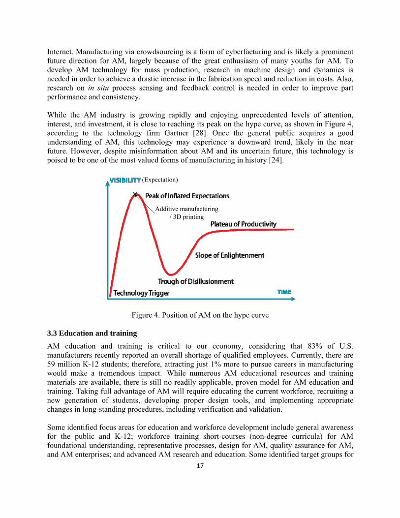
Internet. Manufacturing via crowdsourcing is a form of cyberfacturing and is likely a prominent future direction for AM, largely because of the great enthusiasm of many youths for AM. To develop AM technology for mass production, research in machine design and dynamics is needed in order to achieve a drastic increase in the fabrication speed and reduction in costs. Also, research on in situ process sensing and feedback control is needed in order to improve part performance and consistency. While the AM industry is growing rapidly and enjoying unprecedented levels of attention, interest, and investment, it is close to reaching its peak on the hype curve, as shown in Figure 4, according to the technology firm Gartner [28]. Once the general public acquires a good understanding of AM, this technology may experience a downward trend, likely in the near future. However, despite misinformation about AM and its uncertain future, this technology is poised to be one of the most valued forms of manufacturing in history [24].
(Expectation)
Additive manufacturing / 3D printing
Figure 4. Position of AM on the hype curve
3.3 Education and training
AM education and training is critical to our economy, considering that 83% of U.S. manufacturers recently reported an overall shortage of qualified employees. Currently, there are 59 million K-12 students; therefore, attracting just 1% more to pursue careers in manufacturing would make a tremendous impact. While numerous AM educational resources and training materials are available, there is still no readily applicable, proven model for AM education and training. Taking full advantage of AM will require educating the current workforce, recruiting a new generation of students, developing proper design tools, and implementing appropriate changes in long-standing procedures, including verification and validation. Some identified focus areas for education and workforce development include general awareness for the public and K-12; workforce training short-courses (non-degree curricula) for AM foundational understanding, representative processes, design for AM, quality assurance for AM, and AM enterprises; and advanced AM research and education. Some identified target groups for
18
education and workforce development include the general public; government political leaders and economic development agencies; individual entrepreneurs; and industrial practitioners, including machine operators, technicians, engineers, and business and administration members. Thus far, AM processes and multi-disciplinary teaming have been taught effectively via various curricula. However, several topics such as AM design communication, costing and enterprise-level design decisions, and AM design methodologies, require further development. In addition, education and training personnel must be fully trained, cross-trained to ensure some necessary redundancy, and certified to deliver quality AM components and products. Some key barriers exist to AM education and training. Regarding curriculum development, it is a challenge for four-year colleges to incorporate and integrate manufacturing into the existing curriculum while meeting the Accreditation Board for Engineering and Technology (ABET) requirements; community colleges are focused on relatively low-level technology, and their high-level educational tools are still largely missing, particularly for AM; and, in general, AM education and training materials are still very limited. Regarding equipment affordability, some high-end equipment may be financially out of reach for many community colleges. Regarding the perspective of students, many students are scared of failure, which limits their experimental potential. They also have trouble with clear and concise communication and therefore cannot be put in front of customers. Regarding the perspective of professors, most professors are interested in graduate students; however, 45% of jobs do not require more than a two-year college education. It is critical to train students in two-year colleges on AM machines. 4. RECOMMENDATIONS
Direct fabrication of functional end-use components and products is becoming the main trend of AM technology, and the success with which 3D structural and functional parts consisting of multiple materials and functionally graded materials are being fabricated from various metallic, plastic, ceramic, electronic, composite, and/or biological materials is increasing. However, AM will not replace conventional manufacturing methods for high-volume, low-complexity parts in the foreseeable future. Like many other manufacturing technologies, future AM technology will have more material options, better resolution, faster production, easier and more reliable operation, robust certification, cyber implementation, and lower costs. To facilitate the development and deployment of AM for the future, the following recommendations are proposed. 4.1 Technology and research
For a manufacturing process to be adopted widely by industry, it is critical to have repeatability and consistency of the manufactured parts for the entire build volume, between builds of each machine, and across different machines of the same make. AM technology must be able to guarantee material properties in order to achieve wide industry adoption. Additionally, to broaden and develop new applications, novel AM processes, such as those for bio-applications using cells, biologics, or biomaterials as building blocks and those for micro- and nano-engineering, must be investigated and developed. To achieve these goals, AM technology and its applications require significant further research and development in terms of design, materials, new processes and machines, process modeling, process control, bio-additive manufacturing, and energy and sustainability applications.
19
Based on the technology gaps and research needs discussed in the previous section, some major AM research issues and recommendations have been derived. These are related to and synergistic with the recommendations provided by the 2009 NSF AM Roadmap Workshop report that articulated a future roadmap for AM research [5]. Based on the presentations and discussions in the present workshop, our recommendations for AM technology and research are summarized as follows:
• Materials: Development of new materials for AM processes, formation and mixing of materials in desired forms (powder, ink, slurry, etc.) and with desired properties (viscosity, solids loading, etc.), and understanding of the interaction between materials and processes;
• Design: Methods and tools for simultaneous multi-functional product design and AM process design, methods and tools for assessing lifecycle costs and impacts of AM components and products, and computer-aided design tools for representing complex geometries with repetitive features (e.g., cellular structures), multiple and gradient materials, and other variations;
• Modeling: Robust physics-based mathematical models of temperature, stress, and composition history for understanding transport phenomena in AM processes (e.g., melting and recrystallization behavior in AM of polymers), prediction of microstructures and fatigue properties resulting from extreme heating and cooling rates in AM processes, multi-scale modeling for more accurate prediction of complex process-structure-property relationships, modeling of layer-to-layer bonding between homogeneous and heterogeneous materials, and reduction of complex process models to lower-order models for the purpose of real-time control of AM processes;
• Sensing and control: Fast-response sensors for detecting defects and phase transformation, fast in situ temperature and cooling rate measurements for microstructure prediction, fast in-process optical measurement of geometric dimensions and surface quality of finished layers, in-process multi-band spectroscopic analysis of AM by-products, correlation between model predictions and online measurement of health and quality of AM-fabricated components, and integrated real-time sensing and closed-loop control of AM processes;
• Process innovation: Increase in AM material deposition rate by orders of magnitude for fabrication of large-scale parts, novel bioprinting for simultaneous fulfillment of biophysical, biological, transport, anatomical, and manufacturability requirements, and digital fabrication with digital materials; and
• System integration: Integration of interdisciplinary knowledge rooted in fundamental sciences for AM system development, and cyber-enabled and cloud-based sharing of AM and other manufacturing resources.
A tight coupling exists between material development, process development, process sensing and control, and qualification and certification of products fabricated by AM. As in the progression of many other emerging technologies, the greatest advancements will come at the boundaries of fundamental material science, physics, biology, lasers, electronics, optics, metrology (e.g., computed tomography, 3D scanning, etc.), and control.
20
The production costs, manufacturing time, and part defects must be reduced drastically in order for AM to become hugely successful. The concept of “certify-as-you-build” is beginning to gain traction in industry; this robust and viable approach can cut costs, reduce waste, eliminate defects, and alleviate in situ process problems. It can be used in a variety of industrial sectors to revolutionize current manufacturing and inspection methods, overcome existing manufacturing challenges, and improve industry competitiveness. The outcome will be the elimination of waste and dramatically reduced lead times for the insertion of new products. This may result in a paradigm shift in the manufacturing industry and lead to the revival of manufacturing in the U.S. To provide the technological breakthroughs required to establish the new “certify-as-you-build” manufacturing paradigm, fundamental research (at TRL 1-2 levels) will be needed in order to handle the in situ diagnostics and control of AM processes. Integrating modeling, sensing, and process control will enable the “certify-as-you-build” vision for manufacturing processes. 4.2 University-industry collaboration and technology transfer
Although AM technology recently has experienced significant development, it still is not widely accepted by most industries. Over the next several years, it will be critical to improve the technology to the point of changing people’s mindset and gaining industry acceptance, and to broaden, develop, and identify manufacturing applications that are greatly improved due to or are only possible with AM processes. This will require a substantial increase in university-industry collaboration and technology transfer activities, for which our recommendations are as follows:
• Collaborations incentivized by federal funding programs: In order to speed up the transfer of university research results to industry, meaningful collaborations between academia and industry should be incentivized. It is recommended that NSF significantly increase its funding for university-industry collaboration, through GOALI, SBIR/STTR, PFI, I-Corps, I/UCRC, and other programs. It is also recommended that NIST not only continue but augment its Advanced Manufacturing Technology Consortia (AMTech) program to incentivize the formation and transformation of industry-led consortia by providing resources for leveraging the support of university-industry research that leads to long-term, pre-competitive technology development for the U.S. manufacturing industry.
• Increased federal research and development (R&D) support: To accelerate the development of AM technology, the U.S. government should substantially increase its R&D investments in AM. The investments should include funding from the NSF for fundamental, scientific research and from other federal agencies for mission-oriented research (e.g., DARPA funding to support AM research aimed at DoD applications). This funding increase will be a key to continued AM technology innovation, which is necessary for the U.S. manufacturing industry to remain competitive and for the DoD and other federal departments to benefit from the fruits of AM R&D efforts; and
• Increased coordination efforts for public-private partnerships: Broader coordination of nationwide research efforts in the AM field by academia, industry, and government is needed in order to leverage limited resources and new findings, as well as to minimize duplications. For example, the funding efforts of the NSF and America Makes can be coordinated in the future such that the results of the fundamental, scientific research generated from NSF funding support can be more effectively transitioned to the TRL/MRL 4-7 projects funded by America Makes.
21
4.3 Education and training
4.3.1 University-community college partnership model
AM education and workforce development is a critical area requiring serious consideration. The university-community college partnership model for advanced manufacturing workforce education could bring about a new paradigm for AM education and training. The model has been implemented successfully by the Center for Nanotechnology Education and Utilization (CNEU) and the NSF National Nanotechnology Applications and Career Knowledge (NACK) Network at the Pennsylvania State University. Using this model as the basis, our recommendation for the development of AM education and training is to build partnerships among research universities, 2‐year community and technical colleges, and 4‐year colleges/universities, leading to the creation of viable education pathways for student development through sharing of the following resources:
• Lecture and laboratory experiment sets for AM courses; • Web-accessible lectures (PowerPoint and video formats) to aid partners and other
institutions in offering AM courses; • Educator workshops on how to teach AM courses; • Web access to state‐of‐the‐art tools to enable the teaching of AM at workforce training
institutions, and assistance to instructors in those institutions in learning and using these web-accessible tools;
• Modules for use in introductory AM courses or for general public education; and • Web resources, e.g., webinars, discussion boards, etc.
4.3.2 Teaching factory
Adapting AM in the manufacturing ecosystem requires a well-trained workforce. A model by which to achieve effective AM education is the “teaching factory,” the concept of which is similar to the “teaching hospital” used by the medical profession. In the teaching factory, students are exposed directly to a manufacturing enterprise, where they design products to meet customer needs and manufacture their designed products for the market. The manufacture of these products could utilize a “certify-as-you-build” paradigm. Although capstone design courses required by the current ABET accreditation process offer some sense of real-world design, the projects are often restricted to a subset of research or engineering projects that address short-term needs for participating industrial companies. Teaching factories can eliminate these drawbacks and provide more holistic manufacturing education. Low-cost AM equipment can be used to educate students in the teaching factory, allowing them to fail and become self-reliant through hands-on experiences. It is recommended that support of AM education research and education implementation, such as the teaching factory, be included in future rounds of proposal solicitation topics by America Makes, the NSF, and other federal agencies. 4.3.3 Other education and training efforts
Partnerships between universities/colleges, K-12 schools, and the general public could provide an excellent impetus for AM education and training. Toward this end, we provide the following recommendations:

22
• Promotion of public awareness: This can be achieved by further promoting AM as an exciting technology for making almost anything and as a new tool for advanced manufacturing, as currently portrayed by the public media. One approach could be to use a display/demonstration bus to bring AM technology to the K-12 schools and some public sites (e.g., public libraries);
• Use of the Internet: The Internet can be used to better utilize available resources for outreach through web-based workshops and class demonstrations, to enable remote access of physical equipment for virtual laboratory experiences, and to bring together people from different organizations, such as America Makes, RapidTech, and SME, to develop AM curricula, including certificate programs and integrate with massive open online courses (MOOCs); and
• Establishment of publicly accessible AM facilities: An array of AM facilities could be constructed and made accessible to the public. They could be equipped to fabricate physical parts with different materials from designs submitted by the public. This would stimulate creativity and generate a broad array of design ideas through crowdsourcing, thus enabling the U.S. to continue its long history of innovation. It represents the ultimate democratization of manufacturing.
23
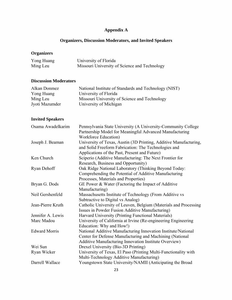
Appendix A
Organizers, Discussion Moderators, and Invited Speakers
Organizers
Yong Huang University of Florida Ming Leu Missouri University of Science and Technology
Discussion Moderators
Alkan Donmez National Institute of Standards and Technology (NIST) Yong Huang University of Florida Ming Leu Missouri University of Science and Technology Jyoti Mazumder University of Michigan
Invited Speakers
Osama Awadelkarim Pennsylvania State University (A University-Community College Partnership Model for Meaningful Advanced Manufacturing Workforce Education)
Joseph J. Beaman University of Texas, Austin (3D Printing, Additive Manufacturing, and Solid Freeform Fabrication: The Technologies and Applications of the Past, Present and Future)
Ken Church Sciperio (Additive Manufacturing: The Next Frontier for Research, Business and Opportunity)
Ryan Dehoff Oak Ridge National Laboratory (Thinking Beyond Today: Comprehending the Potential of Additive Manufacturing Processes, Materials and Properties)
Bryan G. Dods GE Power & Water (Factoring the Impact of Additive Manufacturing)
Neil Gershenfeld Massachusetts Institute of Technology (From Additive vs Subtractive to Digital vs Analog)
Jean-Pierre Kruth Catholic University of Leuven, Belgium (Materials and Processing Issues in Powder Fusion Additive Manufacturing)
Jennifer A. Lewis Harvard University (Printing Functional Materials) Marc Madou University of California at Irvine (Re-engineering Engineering
Education: Why and How!) Edward Morris National Additive Manufacturing Innovation Institute/National
Center for Defense Manufacturing and Machining (National Additive Manufacturing Innovation Institute Overview)
Wei Sun Drexel University (Bio-3D Printing) Ryan Wicker University of Texas, El Paso (Printing Multi-Functionality with
Multi-Technology Additive Manufacturing) Darrell Wallace Youngstown State University/NAMII (Anticipating the Broad

24
Implications of Additive Manufacturing on Workforce Development and Education)
25
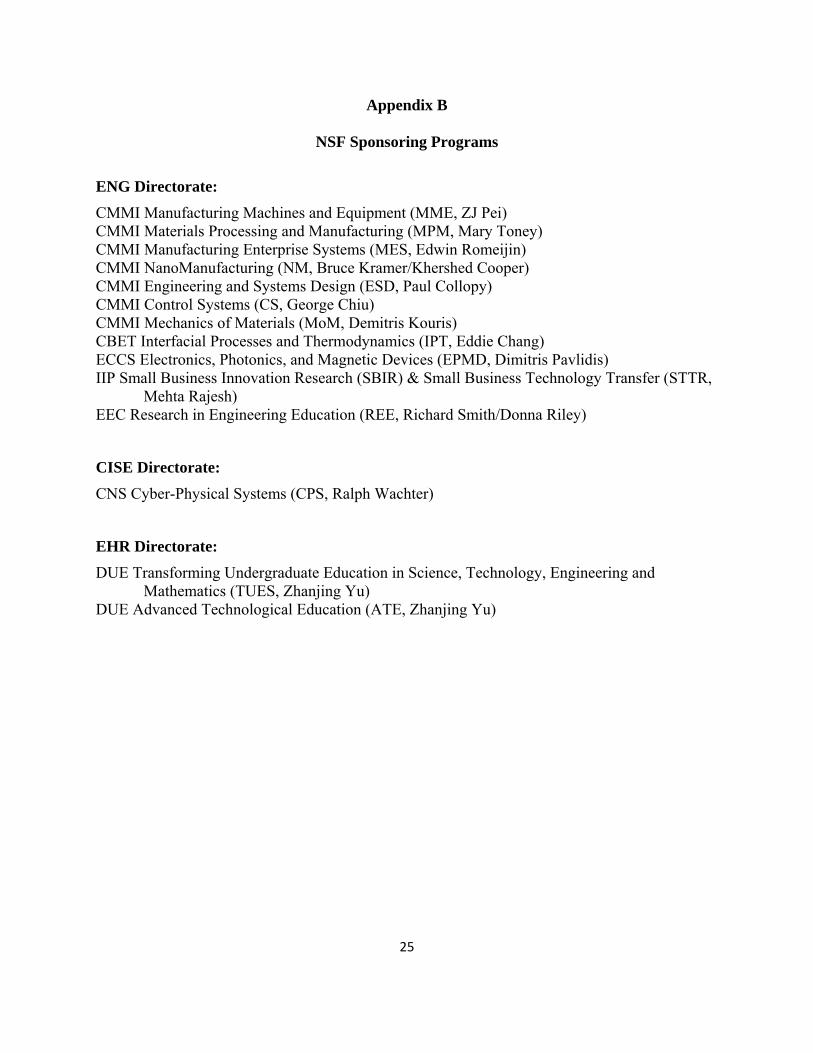
Appendix B
NSF Sponsoring Programs
ENG Directorate:
CMMI Manufacturing Machines and Equipment (MME, ZJ Pei) CMMI Materials Processing and Manufacturing (MPM, Mary Toney) CMMI Manufacturing Enterprise Systems (MES, Edwin Romeijin) CMMI NanoManufacturing (NM, Bruce Kramer/Khershed Cooper) CMMI Engineering and Systems Design (ESD, Paul Collopy) CMMI Control Systems (CS, George Chiu) CMMI Mechanics of Materials (MoM, Demitris Kouris) CBET Interfacial Processes and Thermodynamics (IPT, Eddie Chang) ECCS Electronics, Photonics, and Magnetic Devices (EPMD, Dimitris Pavlidis) IIP Small Business Innovation Research (SBIR) & Small Business Technology Transfer (STTR,
Mehta Rajesh) EEC Research in Engineering Education (REE, Richard Smith/Donna Riley)
CISE Directorate:
CNS Cyber-Physical Systems (CPS, Ralph Wachter)
EHR Directorate:
DUE Transforming Undergraduate Education in Science, Technology, Engineering and Mathematics (TUES, Zhanjing Yu)
DUE Advanced Technological Education (ATE, Zhanjing Yu)
26
References Cited
[1] ASTM International Committee F42 on Additive Manufacturing Technologies, ASTM F2792–10 Standard Terminology for Additive Manufacturing Technologies, West Conshohocken, PA, 2009.
[2] F.B. Prinz, C.L. Atwood, R.F. Aubin, J.J. Beaman, R.L. Brown, P.S. Fussell, A.J. Lightman, E. Sachs, L.E. Weiss, and M.J. Wozny, JTEC/WTEC Panel Report on Rapid Prototyping in Europe and Japan, World Technology Evaluation Center, Baltimore, 1997.
[3] National Center for Manufacturing Sciences, The Road to Manufacturing: 1998 Industrial Roadmap for the Rapid Prototyping Industry, NCMS Report 0199RE98, Ann Arbor, MI, June 30, 1998.
[4] J.J. Beaman, C. Atwood, T.L. Bergman, D.L. Bourell, S. Hollister, and D. Rosen, WTEC Panel Report on Additive/Subtractive Manufacturing Research in Europe, World Technology Evaluation Center, Baltimore, MD, 2003.
[5] D.L. Bourell, M. Leu, and D. Rosen, Roadmap for Additive Manufacturing - Identifying the Future of Freeform Processing, Univ. of Texas, Austin, TX, 2009.
[6] Wohlers Associates, Inc., Wohlers Report 2013: Additive Manufacturing and 3D Printing State of the Industry, Fort Collins, Colorado, 2013.
[7] D.L. Bourell, J.J. Beaman, M.C. Leu, and D.W. Rosen, 2009, “A Brief History of Additive Manufacturing and the 2009 Roadmap for Additive Manufacturing: Looking Back and Looking Ahead,” Proceedings of RapidTech 2009: US-TURKEY Workshop on Rapid Technologies, pp. 1-8.
[8] J.P. Kruth, M.C. Leu, and T. Nakagawa, 1998, “Progress in Additive Manufacturing and Rapid Prototyping,” CIRP Annals- Manufacturing Technology, Vol. 47(2), pp. 525–540.
[9] N. Guo and M.C. Leu, 2013, “Additive Manufacturing: Technology, Applications and Research Needs,” Front. Mech. Eng., Vol. 8(3), pp. 215–243.
[10] Optomec, http://www.optomec.com/
[11] V. Mironov, R.P. Viconti, V. Kasyanov, G. Forgacs, C.J. Drake, and R.R. Markwald, 2009, “Organ Printing: Tissue Spheroids as Building Blocks,” Biomaterials, Vol. 30(12), pp. 2164-2174.
[12] B.R. Ringeisen, R.K. Pirlo, P.K. Wu, T. Boland, Y. Huang, W. Sun, Q. Hamid, and D.B. Chrisey, 2013, “Cell and Organ Printing Turns 15: Diverse Research to Commercial Transitions,” MRS Bulletin, Vol. 38(10), pp. 834-843.
[13] B.C. Riggs, A.D. Dias, N.R. Schiele, R. Cristescu, Y. Huang, D.T. Corr, and D.B. Chrisey, 2011, “Matrix-Assisted Pulsed Laser Methods for Biofabrication,” MRS Bulletin, Vol. 36(12), pp. 1043-1050.
[14] C. Xu, W. Chai, Y. Huang, and R.R. Markwald, 2012, “Scaffold-free Inkjet Printing of Three-dimensional Zigzag Cellular Tubes,” Biotechnol. Bioeng., Vol. 109(12), pp. 3152-3160.
27
[15] NIST, Measurement Science Roadmap for Metal-Based Additive Manufacturing, Gaithersburg, MD, 2013.
[16] S. Kalpakjian and S.R. Schmid, Manufacturing Processes for Engineering Materials, 5th Ed., Prentice Hall, Upper Saddle River, NJ, 2008.
[17] J. Scott, N. Gupta, C. Weber, S. Newsome, T. Wohlers, and T. Caffrey, Additive Manufacturing: Status and Opportunities, Science and Technology Policy Institute, Washington, D.C., 2012.
[18] Makerspace, http://makerspace.com/
[19] I. Gibson, D.W. Rosen, and B. Stucker, Additive Manufacturing Technologies: Rapid Prototyping to Direct Digital Manufacturing, Springer, New York, NY, 2010.
[20] Center for BioMolecular Modeling, http://cbm.msoe.edu/
[21] The Economist, Manufacturing: The Third Industrial Revolution, London, UK, April, 2012.
[22] T.R. Jackson, H. Liu, N.M. Patrikalakis, E.M. Sachs, and M.J. Cima, 1999, “Modelling and Designing Functionally Graded Material Components for Fabrication with Local Composition Control,” Materials & Design, Vol. 20(2-3), pp. 63-75.
[23] F. Liou, K. Slattery, M. Kinsella, J. Newkirk, H.N. Chou, and R. Landers, 2007, “Applications of a Hybrid Manufacturing Process for Fabrication of Metallic Structures,” Rapid Prototyping Journal, Vol. 13(4), pp. 236-244.
[24] T. Wohlers and T. Caffrey, 2013, “Additive Manufacturing: Going Mainstream,” Manufacturing Engineering, June, pp. 67-73.
[25] G.A. Popescu, T. Mahale, and N. Gershenfeld, 2006, “Digital Material for Digital Printing,” Proceedings of Digital Fabrication 2006, Denver, Colorado, USA, pp. 55-57.
[26] J. Hiller and H. Lipson, 2010, “Tunable Digital Material Properties for 3D Voxel Printers,” Rapid Prototyping Journal, Vol. 16(4), pp. 241-247.
[27] K.C. Cheung and N. Gershenfeld, 2013, “Reversibly Assembled Cellular Composite Materials,” Science, Vol. 341, pp. 1219-1221.
[28] http://www.treehugger.com/sustainable-product-design/tech-consultancy-puts-3d-printing-peak-hype-cycle.html, accessed February, 2014.