a novel two-split capacitor array with linearity analysis ... novel two-split capacitor array with...
TRANSCRIPT
A Novel Two-Split Capacitor Array with
Linearity Analysis for High-Resolution SAR
ADCs
Yingxin Zheng, Zongmin Wang, Song Yang, Qizhang Li, and Li Xiang Beijing Microelectronics Tech. Institution (BMTI), Beijing, China
Email: [email protected]
Abstract—A novel two-split capacitor (T-SC) array
structure for Successive Approximation Register (SAR)
analog-to-digital converter (ADC) is proposed. When used
as digital –to-analog converter (DAC), this circuit reduced
the chip area by 27.7% in comparing with the conventional
Split Capacitor (SC) at resolution=14. The area reduction
effect can be more significant with the increasing resolution
of ADC. The capacitor mismatch and parasitic effects of this
proposed structure are analyzed in theory. Behavioral
simulations were performed to demonstrate the effectiveness
of this proposed structure. This simulation was only
performed for capacitor mismatch. Simulation results show
that T-SC array could achieve good binary-weighted
performance and the standard deviation of its DNL was
0.51LSB when the standard deviation of capacitor was
0.025%. Furthermore, the analysis in this paper is provided
for designers to make a tradeoff among resolution, CMOS
process, circuit structure and capacitor size in their design
of SAR ADC.
Index Terms—capacitor DAC, capacitor mismatch,
nonlinearity, SAR ADC, small area
I. INTRODUCTION
Recently, the Successive Approximation Register
(SAR) analog-to-digital converter (ADC) has attracted
more attentions again for that it features low power and
area consumption due to its simple structure and least
usage of analog circuit. Thus, it is used widely in today’s
System-on-Chip (SOC) solutions [1], [2], where requires
low power, low cost, high speed and high density. As we
all know, capacitor array DAC (CDAC) is used popularly
in SAR ADC. For a binary-weighted capacitor array, as
the resolution increases, a problem comes up: the total
number of capacitors in CDAC will has an exponential
increase. This will lead to increasing chip area, power
dissipation as well as reducing speed due to a large
charging time-constant. Obviously, it does not match case
of SOC’s requirements. To mitigate this problem, split
capacitor array is used, which can reduce total number of
capacitors. However, when the resolution is higher, this
problem still exists and cannot be ignored.
This paper presents a novel two-split capacitor (T-SC)
array structure based on conventional SC array. When
Manuscript received April 25, 2014; revised June 27, 2014.
used as digital-to-analog converter (DAC), this circuit
reduced the chip area by 27.7% in comparing with the
conventional Split Capacitor (SC) at resolution=14.
Notably, the high speed performance advantage did not
go away. The area reduction effect can be more
significant with the increasing resolution of ADC. Thus,
it can be used widely in high-speed and medium-to-high
resolution SAR ADC. Because the data of the capacitor
mismatch are usually available in statistical data, such as
standard deviation [3], it is more practical to clarify the
relationship between the standard deviation of the
capacitor mismatch and the achievable ADC accuracy. In
this paper, a statistical analysis has been made on the
effect of capacitor mismatch on the SAR ADC resolution
for these two capacitor array structure. Also, the roughly
analysis of parasitic effect is included in this paper.
II. OVERVIEW OF SAR ADC OPERATION
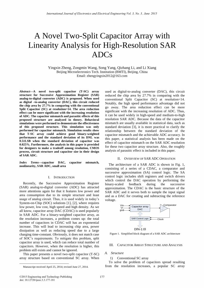
The architecture of a SAR ADC is shown in Fig. 1,
consisting of a series of a CDAC, a comparator and
successive approximation (SA) control logic. The SA
control logic includes shift registers and switch drivers
which control the DAC operation by performing the
binary-scaled feedback during the successive
approximation. The CDAC is the basic structure of the
SAR ADC and it serves both to sample the input signal
and as a DAC for creating and subtracting the reference
voltage.
Capacitor array
DAC
SAR Control Logic
VinVr
gnd
Clock
Comparator
D[N-1:0]
Figure 1. Simplified block diagram of a SAR ADC architecture
III. CAPACITOR ARRAY STRUCTURE AND ANALYSIS
A. Structure
1) Conventional SC array
To solve the problem of capacitors spread resulting
from the resolution increases, a popular SC array
©2015 Engineering and Technology Publishing 177doi: 10.12720/ijeee.3.3.177-181
International Journal of Electronics and Electrical Engineering Vol. 3, No. 3, June 2015
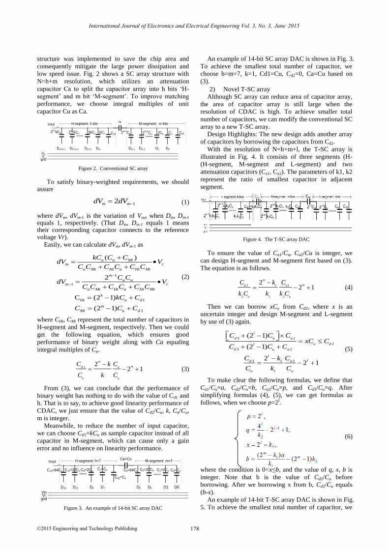
structure was implemented to save the chip area and
consequently mitigate the large power dissipation and
low speed issue. Fig. 2 shows a SC array structure with
N=h+m resolution, which utilizes an attenuation
capacitor Ca to split the capacitor array into h bits ‘H-
segment’ and m bit ‘M-segment’. To improve matching
performance, we choose integral multiples of unit
capacitor Cu as Ca.
...... ......2
h-1kCu 2
h-2kCu 2kCu kCu Cd1 2
m-1Cu 2
m-2Cu 2Cu Cu Cd2
Ca
Vout H-segment: h bits M-segment: m bits
Dm+h-1 Dm+h-2 Dm+1 Dm Dm-1 Dm-2 D1 D0
VinVr
gnd
Figure 2. Conventional SC array
To satisfy binary-weighted requirements, we should assure
12m mdV dV (1)
where dVm, dVm-1 is the variation of Vout when Dm, Dm-1 equals 1, respectively. (That Dm, Dm-1 equals 1 means their corresponding capacitor connects to the reference voltage Vr).
Easily, we can calculate dVm, dVm-1 as
1
1
Ht 1
2
( )
2
C (2 1)
(2 1)
u a Mtm r
a Mt Ht a Ht Mt
m
u am r
a Mt Ht a Ht Mt
h
u d
m
Mt u d
kC C CdV V
C C C C C C
C CdV V
C C C C C C
kC C
C C C
(2)
where CHt, CMt represent the total number of capacitors in
H-segment and M-segment, respectively. Then we could
get the following equation, which ensures good
performance of binary weight along with Ca equaling
integral multiples of Cu.
22
2 1
m
md a
u u
C Ck
C k C
(3)
From (3), we can conclude that the performance of
binary weight has nothing to do with the value of Cd1 and
h. That is to say, to achieve good linearity performance of
CDAC, we just ensure that the value of Cd2/Cu, k, Ca/Cu,
m is integer.
Meanwhile, to reduce the number of input capacitor,
we can choose Cd1=kCu as sample capacitor instead of all
capacitor in M-segment, which can cause only a gain
error and no influence on linearity performance.
...... ......C13=64Cu C12=32Cu C8=2Cu
C7=Cu
Cd1=Cu
C6=64Cu C5=32Cu C1=2Cu C0=Cu
Ca=CuVout H-segment: h=7 M-segment: m=7
D13 D12 D8 D7 D6 D5 D1 D0
VinVr
gnd
Figure 3. An example of 14-bit SC array DAC
2) Novel T-SC array
Although SC array can reduce area of capacitor array,
the area of capacitor array is still large when the
resolution of CDAC is high. To achieve smaller total
number of capacitors, we can modify the conventional SC
array to a new T-SC array.
Design Highlights: The new design adds another array
of capacitors by borrowing the capacitors from Cd2.
With the resolution of N=h+m+l, the T-SC array is
(H-segment, M-segment and L-segment) and two
attenuation capacitors (Ca1, Ca2). The parameters of k1, k2
represent the ratio of smallest capacitor in adjacent
segment.
Figure 4. The T-SC array DAC
To ensure the value of Ca1/Cu, Ca2/Cu is integer, we
can design H-segment and M-segment first based on (3).
The equation is as follows.
2 11
2 1 2
22 1
m
md a
u u
C Ck
k C k k C
(4)
Then we can borrow xCu from Cd2, where x is an
uncertain integer and design M-segment and L-segment
by use of (3) again.
3 2
2
3 2
3 21
1
(2 1)
(2 1)
2 2 1
l
d u a
u dl
d u a
l
ld a
u u
C C CxC C
C C C
C Ck
C k C
(5)
To make clear the following formulas, we define that
Ca1/Cu=a, Cd2/Cu=b, Ca2/Cu=p, and Cd3/Cu=q. After
simplifying formulas (4), (5), we can get formulas as
follows, when we choose p=2l.
(6)
©2015 Engineering and Technology Publishing 178
International Journal of Electronics and Electrical Engineering Vol. 3, No. 3, June 2015
-
illustrated in Fig. 4. It consists of three segments (H-
An example of 14-bit SC array DAC is shown in Fig. 3.
To achieve the smallest total number of capacitor, we
choose h=m=7, k=1, Cd1=Cu, Cd2=0, Ca=Cu based on
(3).
where the condition is 0<x≤b, and the value of q, x, b is
integer. Note that b is the value of Cd2/Cu before
borrowing. After we borrowing x from b, Cd2/Cu equals
(b-x).
An example of 14-bit T-SC array DAC is shown in Fig.
5. To achieve the smallest total number of capacitor, we
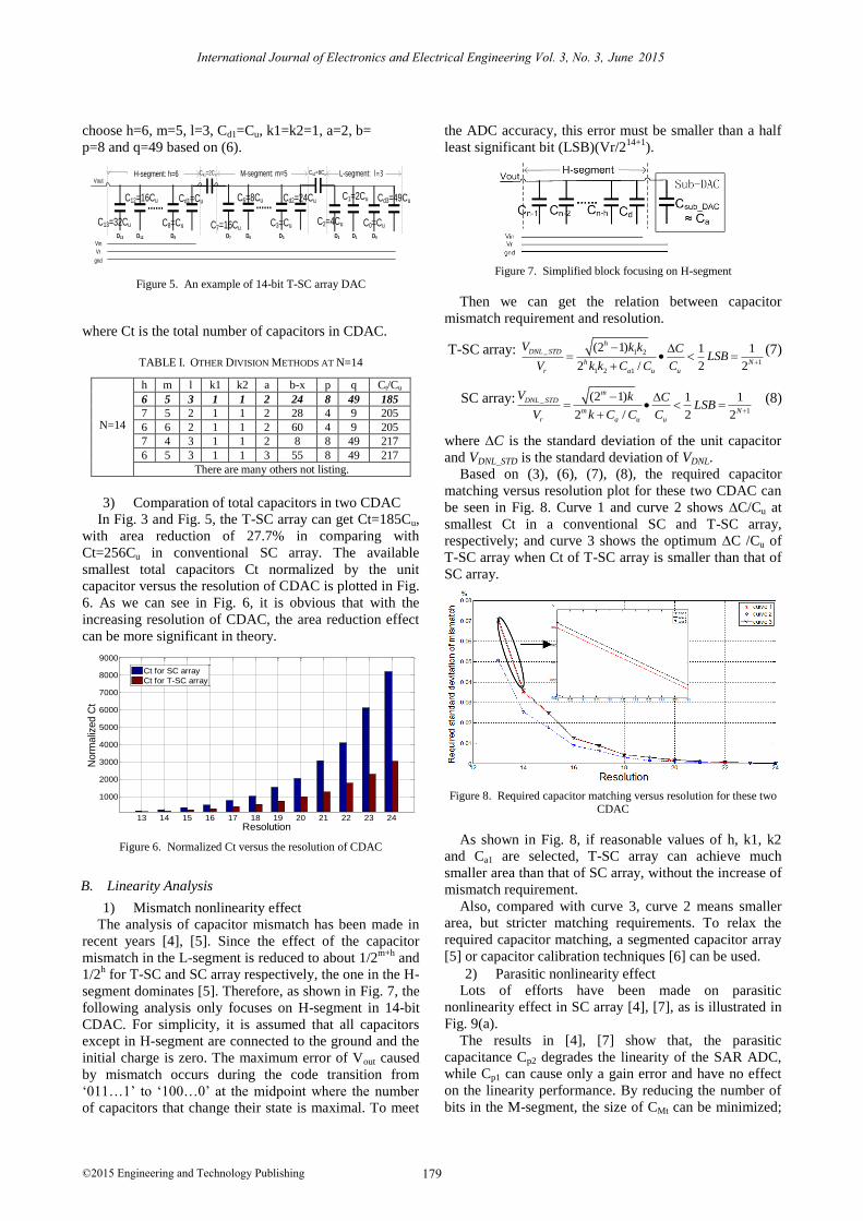
©2015 Engineering and Technology Publishing 179
International Journal of Electronics and Electrical Engineering Vol. 3, No. 3, June 2015
choose h=6, m=5, l=3, Cd1=Cu, k1=k2=1, a=2, b=
p=8 and q=49 based on (6).
......
C7=16Cu
C6=8Cu
C3=Cu
Cd2=24Cu
C2=4Cu
C1=2Cu
C0=Cu
Cd3=49Cu
Ca2=8Cu
VoutM-segment: m=5 L-segment: l=3
Vin
Vr
gnd
......
C13=32Cu
C12=16Cu
C8=Cu
Cd1=Cu
Ca1=2CuH-segment: h=6
D13 D12 D8 D7 D6 D3 D2 D1 D0
Figure 5. An example of 14-bit T-SC array DAC
where Ct is the total number of capacitors in CDAC.
TABLE I. OTHER DIVISION METHODS AT N=14
N=14
h m l k1 k2 a b-x p q Ct/Cu
6 5 3 1 1 2 24 8 49 185
7 5 2 1 1 2 28 4 9 205
6 6 2 1 1 2 60 4 9 205
7 4 3 1 1 2 8 8 49 217
6 5 3 1 1 3 55 8 49 217
There are many others not listing.
3) Comparation of total capacitors in two CDAC
In Fig. 3 and Fig. 5, the T-SC array can get Ct=185Cu,
with area reduction of 27.7% in comparing with
Ct=256Cu in conventional SC array. The available
smallest total capacitors Ct normalized by the unit
capacitor versus the resolution of CDAC is plotted in Fig.
6. As we can see in Fig. 6, it is obvious that with the
increasing resolution of CDAC, the area reduction effect
can be more significant in theory.
13 14 15 16 17 18 19 20 21 22 23 24
1000
2000
3000
4000
5000
6000
7000
8000
9000
Resolution
Norm
aliz
ed C
t
Ct for SC array
Ct for T-SC array
Figure 6. Normalized Ct versus the resolution of CDAC
B. Linearity Analysis
1) Mismatch nonlinearity effect
The analysis of capacitor mismatch has been made in
recent years [4], [5]. Since the effect of the capacitor
mismatch in the L-segment is reduced to about 1/2m+h
and
1/2h
for T-SC and SC array respectively, the one in the H-
segment dominates [5]. Therefore, as shown in Fig. 7, the
following analysis only focuses on H-segment in 14-bit
CDAC. For simplicity, it is assumed that all capacitors
except in H-segment are connected to the ground and the
initial charge is zero. The maximum error of Vout caused
by mismatch occurs during the code transition from
‘011…1’ to ‘100…0’ at the midpoint where the number
of capacitors that change their state is maximal. To meet
the ADC accuracy, this error must be smaller than a half
least significant bit (LSB)(Vr/214+1
).
Figure 7. Simplified block focusing on H-segment
Then we can get the relation between capacitor
mismatch requirement and resolution.
T-SC array: _ 1 2
1
1 2 1
(2 1) 1 1
2 / 2 2
h
DNL STD
h N
r a u u
V k k CLSB
V k k C C C
(7)
SC array: _
1
(2 1) 1 1
2 / 2 2
mDNL STD
m N
r a u u
V k CLSB
V k C C C
(8)
where ∆C is the standard deviation of the unit capacitor
and VDNL_STD is the standard deviation of VDNL.
Based on (3), (6), (7), (8), the required capacitor
matching versus resolution plot for these two CDAC can
be seen in Fig. 8. Curve 1 and curve 2 shows ∆C/Cu at
smallest Ct in a conventional SC and T-SC array,
respectively; and curve 3 shows the optimum ∆C /Cu of
T-SC array when Ct of T-SC array is smaller than that of
SC array.
Figure 8. Required capacitor matching versus resolution for these two CDAC
As shown in Fig. 8, if reasonable values of h, k1, k2
and Ca1 are selected, T-SC array can achieve much
smaller area than that of SC array, without the increase of
mismatch requirement.
Also, compared with curve 3, curve 2 means smaller
area, but stricter matching requirements. To relax the
required capacitor matching, a segmented capacitor array
[5] or capacitor calibration techniques [6] can be used.
2) Parasitic nonlinearity effect
Lots of efforts have been made on parasitic
nonlinearity effect in SC array [4], [7], as is illustrated in
Fig. 9(a).
The results in [4], [7] show that, the parasitic
capacitance Cp2 degrades the linearity of the SAR ADC,
while Cp1 can cause only a gain error and have no effect
on the linearity performance. By reducing the number of
bits in the M-segment, the size of CMt can be minimized;
©2015 Engineering and Technology Publishing 180
International Journal of Electronics and Electrical Engineering Vol. 3, No. 3, June 2015
thus the nonlinearity effect can be alleviated. But this will
enlarge the capacitor spread in H-segment.
As we all know, bottom-plate parasitic capacitance of a
capacitor is bigger than that of top-plate. Thus, using
results in [4], [7], capacitors in T-SC array can be
distributed in Fig. 9(b), which can reduce the parasitic
effect. To alleviate the parasitic effect further, the number
of bits in the L-segment and M-segment should be chosen
carefully with other parameters.
Cp2 CMt
VoutM-segment
Cp1
CaH-segment
CHt
CLt
Vout
CMtCHt
Ca2Ca1
(a)
(b)
Figure 9. Analysis of parasitic nonlinearity effect in SC and T-SC array
IV. SIMULATION RESULTS
A. Binary-Weighted Performance
To verify binary-weighted performance of T-SC array,
the example in Fig. 5 is simulated at Vr=1V from
D=‘00…01’, ‘00…10’ to ‘10…00’. As shown in Fig. 10,
the results match the theoretical analysis perfectly.
Figure10. Binary-weighted performance
B. Behavioral Simulation For Capacitor Mismatch
In Fig. 5, to ensure VDNL_STD is smaller than 1/2LSB,
the theoretical value of capacitor mismatch is ∆C /Cu
<0.025% for T-SC array.
Behavioral simulation of T-SC array in Fig. 5 is
performed to verify the previous analysis. In simulation,
it is assumed that the unit capacitor has a Gaussian
distribution with standard deviation of 0.025% (∆C /Cu
<0.025%). Fig. 11 shows the result of 3000-time Monte
Carlo runs, where the standard deviation of DNL and INL
is plotted versus input code of CDAC. As expected, the
maximum value of DNL is 0.51LSB, a little bigger than
1/2LSB.
Figure 11. The standard deviation of DNL, INL versus input code of
CDAC
V. CONCLUSION
A novel two-split capacitor array has been proposed
which can achieve area reduction effect in comparison
with SC array. Theoretical analysis of the linearity
performance was verified by comparing with the Monte-
Carlo simulation results. Furthermore, the analysis in this
paper is provided for designers to make a tradeoff among
resolution, CMOS process, and capacitor area in their
design of SAR ADC.
REFERENCES
[1] M. D. Scott, B. E. Boser, and K. S. J. Pister, “An ultralow_energy ADC for smart dust,” IEEE J. Solid-State Circuits, vol. 38, pp.
1123-1129, 2003.[2] T.-C. Huang, P.-T. Huang, S.-L. Wu, et al., “Area-Power-Efficient
11-bit SAR ADC with delay-line enhanced tuning for neural
sensing applications,” in Proc. IEEE Biomedical Circuits and Systems Conference, 2013, pp. 238-241.
[3] A. Verma and B. Razavi, “Frequency-Based measurements of
mismatches between small capacitors,” in Proc. CICC, 2006, pp. 481-484.
[4] Y. Zhu, U. Chio, H.-G. Wei, et al., “Linearity analysis on a series-split capacitor array for high-speed SAR ADCs,” in Proc.
International Midwest Symposium on Circuits and Systems, 2008,
pp. 922-925.[5] T. Wakimoto, H. Li, and K. Murase, “Statistical analysis on the
effect of capacitance mismatch in a high-resolution successive-approximation ADC,” IEEJ Trans. Electr. Electron. Eng., vol. 6,
pp. S89-S93, 2011.
[6] H. Neubauer, T. Desel, and H. Hauer, “A successive approximation A/D converter with 16bit 200kS/s in 0.6um CMOS
using selfcalibration and low power techniques,” in Proc. 8th IEEE Int. Conf. Electronics, Circuits and Systems, 2001, pp. 859-
862.
[7] S. Lei, D. Qin yuan, L. Chuangchuan, and Q. Gaoshuai, “Analysis on capacitor mismatch and parasitic capacitors effect of improved
segmented-capacitor array in SAR ADC,” in Proc. IITA, 2009, pp. 280-283.
Yingxin Zheng was born in 1990, China. He is currently pursuing the
M.S. in Microelectronics Engineering at Beijing Microelectronics Tech Institution. His research focus is in High-speed/High-resolution Analog
to Digital converter design, and he is talented in the development of
chip area reduction techniques.He joined the High-speed/High-resolution Analog to Digital Converter
design group in 2012. In just two years, his talents and work have been recognized by leaders in this field.
Zongmin Wang was born in 1973, China. He received the M.S. degree in Electrical Engineering from the Harbin Institute of Technology. He is
dedicated to the research of ADC and DAC, and currently serves as a
student advisor. Many of his work are highly praised.
Song Yang was born in 1973, China. He received his PhD degree from the Science Academy of China, Yunnan Branch, 2008’, in automation
modernization. He joined this A/D converter research group in 2008.
Upon his coming, he brought along industry insight and an upper level system view.
Qizhang Li was born in 1986, China. He received the M.S. in Analog Signal Circuits Design from Beijing Jiaotong University 12’. He joined
this High-Speed/High-Resolution A/D converter research group in 2012.
He is dedicated to the research of Analog to Digital converter design.
Li Xiang was born in 1989, China. He received his M.S.E. in Systems Engineering from the University of Pennsylvania 14’. He joined this
High-Speed/High-Resolution A/D converter research group in 2014.
©2015 Engineering and Technology Publishing 181
International Journal of Electronics and Electrical Engineering Vol. 3, No. 3, June 2015