reduced-code static linearity test of split-capacitor sar
TRANSCRIPT

HAL Id: hal-01989117https://hal.archives-ouvertes.fr/hal-01989117
Submitted on 17 Jul 2020
HAL is a multi-disciplinary open accessarchive for the deposit and dissemination of sci-entific research documents, whether they are pub-lished or not. The documents may come fromteaching and research institutions in France orabroad, or from public or private research centers.
L’archive ouverte pluridisciplinaire HAL, estdestinée au dépôt et à la diffusion de documentsscientifiques de niveau recherche, publiés ou non,émanant des établissements d’enseignement et derecherche français ou étrangers, des laboratoirespublics ou privés.
Distributed under a Creative Commons Attribution - NonCommercial| 4.0 InternationalLicense
Reduced-code static linearity test of split-capacitor SARADCs using an embedded incremental Sigma-Delta
converterR. Silveira Feitoza, Manuel J. Barragan, Daniel Dzahini, Salvador Mir
To cite this version:R. Silveira Feitoza, Manuel J. Barragan, Daniel Dzahini, Salvador Mir. Reduced-code static linearitytest of split-capacitor SAR ADCs using an embedded incremental Sigma-Delta converter. IEEETransactions on Device and Materials Reliability, Institute of Electrical and Electronics Engineers,2019, �10.1109/TDMR.2019.2891298�. �hal-01989117�

IEEE TRANSACTIONS ON DEVICE AND MATERIALS RELIABILITY, VOL. X, NO. X, MONTH 2019 1
Reduced-code static linearity test of split-capacitorSAR ADCs using an embedded incremental Σ∆
converterRenato S. Feitoza, Student Member, IEEE, Manuel J. Barragan, Member, IEEE,
Daniel Dzahini, Member, IEEE, and Salvador Mir, Member IEEE
Abstract—Reduced-code techniques for ADC static linearitytest have the potential to drastically reduce the number ofnecessary measurements for a complete static linearity char-acterization. These techniques take advantage of the repetitiveoperation of certain families of converters such as pipelines,SARs, cyclic, etc. In this paper we present a novel reduced-code technique for the static linearity test of split-capacitor SARADCs based on the on-chip generation and measurement of themajor carrier transitions of the input DAC of the converter.The proposed test method does not require a test stimulus,and we show that the necessary measurements can be easilyextracted by reconfiguring portions of the SAR into a low-resolution Incremental Σ∆ converter. The proposed techniqueis validated with both behavioral and electrical simulations of a10-bit SAR ADC in a 65 nm CMOS technology.
Index Terms—Analog-to-Digital Conversion; Design-for-Test;Static Linearity Test; Reduced-code testing.
I. INTRODUCTION
DUE to CMOS technology scaling, Successive-Approximation Register Analog-to-Digital Converters
(SAR ADCs) have paved their way back to the spotlightof both academic and industrial efforts. One of the mainreasons for that is their ability to go on sleep mode and itsoverall energy efficiency, that are crucial in several emergingapplications [1]. Additionally, since the architecture of a SARADC relies on few analog blocks in comparison to otherarchitectures, it is known to be a digital-friendly topology, andhence the advantages of scaling are leveraged very efficiently.
In that context, the split-capacitor SAR (SC-SAR) ADChas been shown to provide an even better compromise interms of area, power consumption and speed. The majorcontributor to the area of a capacitor-based SAR ADC isthe Capacitive Digital-to-Analog Converter (CDAC) that isused for approximating the analog input samples of the SARADC. Due to the fact that a split capacitor SAR uses two(or more) CDAC arrays separated by bridge capacitors ratherthan just one binary-weighted CDAC, the area occupied by thecapacitors is greatly reduced [2]. Yet, capacitor-based SARADCs are very prone to static errors, and the main sourceof these errors are the mismatches in the DAC capacitive
R. S. Feitoza, M. J. Barragan, D. Dzahini and S. Mir are with UniversiteGrenoble Alpes, CNRS, Grenoble INP, TIMA, 38000, Grenoble, France (e-mail: [email protected]).
array. Moreover, it has been shown that this issue is evenmore critical for split-capacitor SC-SAR ADCs due to theparasitic capacitances of the bridge attenuation capacitors [3].Static linearity tests are then necessary in order to assure thecorrect functionality of the converter. However, static test canbe a very demanding and costly task. Indeed, the mixed-signalsections of a complex System-on-Chip (SoC) are amongst themore critical in terms of test time [4], and to complicate thingseven more, relative test cost is increased with further tech-nology scaling. Focusing specifically on ADC/DAC testing,the paramount issues are the need of an accurate and lineartest stimulus and the huge volume of samples that have to becollected in order to perform an accurate measurement. Thestandard in industry is the histogram test method, in which thewhole set of codes available on the ADC/DAC is measured [5].This leads to a number of samples that scales exponentiallywith the resolution of the ADC/DAC. In order to average noiseeach code has to be measured a few times, which furtherincreases the total test time. The development of techniques toreduce test time is a critical task, since they enable not onlyspeeding-up and reducing test cost, but they also open the doorto enhanced reliability during the lifetime of the circuit.
In recent years, the development of the so-called reduced-code techniques have been drawing attention due to thepotential to yield large reductions in test time. They rely onthe repetitive operation of some ADC topologies, where errorsacross the ADC transfer function are caused by a reduced setof components. This allows inferring the complete transferfunction of the ADC by measuring only a carefully selectedsubset of the total set of codes, greatly reducing the global testtime. Moreover, the inherent simplification of static linearitytests provided by reduced-code techniques may open the doorto a full built-in self-test (BIST) implementation. This way,tester requirements can be relaxed and test cost may be furthercontained by moving static linearity test resources to thedevice under test itself. Furthermore, BIST techniques mayenable on-line test, self-healing, self-calibration and adaptiveoperation in safety-critical and mission-critical applications.Indeed, reliability and quality enhancement is becoming oneof the main drivers for the development of analog and mixed-signal BIST. For instance, in safety-critical applications, suchas automotive, mixed-signal BIST is even becoming a designrequirement in many integrated systems.
In this direction, the work in [6] estimates the full non-linearity characteristic of a SAR converter by measuring aCopyright c© 2019 IEEE. Personal use of this material is permitted.
However, permission to use this material for any other purposes mustbe obtained by sending a request to [email protected]
This is the author's version of an article that has been published in this journal. Changes were made to this version by the publisher prior to publication.The final version of record is available at http://dx.doi.org/10.1109/TDMR.2019.2891298
Copyright (c) 2019 IEEE. Personal use is permitted. For any other purposes, permission must be obtained from the IEEE by emailing [email protected].

IEEE TRANSACTIONS ON DEVICE AND MATERIALS RELIABILITY, VOL. X, NO. X, MONTH 2019 2
smaller set of codes through the application of a piecewiselinear ramp on the ADC input. The main problem with thatapproach is that the generation of this type of excitation maybe challenging. Another limitation is that missing codes maynot be detected. Examples of reduced-code techniques forpipeline ADCs can be found in [7] and [8], while a model-based reduced-code strategy is proposed in [9]. In [10], a bitweight extraction based on the measurement of the Major Car-rier Transitions (MCTs) of the CDAC is proposed. The MCTsare generated using a modified SAR operation and measuredusing an auxiliary CDAC for test, similarly to the approachof self-calibration proposed in [11]. However, that approach isonly convenient for sub-radix calibration applications since thevalue of the unit capacitor has to be changed, unbalancing theweights of the CDAC. This technique is also very susceptibleto the capacitor mismatch in the auxiliary CDAC.
For SC-SAR ADCs, the focus in the existing literature hasbeen more on the calibration of the capacitive mismatchesthan in characterizing the static non-linearity of the converter.In works such as [3], [12], [13], a tunable capacitor is added inparallel with the LSB array to compensate for the mismatches,but no static linearity information is explicitly extracted. In[2], a differential SC-SAR ADC is tested in such a way thatone branch is responsible for the measurement of the adjacentbranch. There, only the MSB capacitors are characterized.The main advantage of this approach is that no extra analogcircuitry is needed to perform the measurements. Similarly, in[14] one sub-array is responsible for the bit weight extractionof the other. The main disadvantage of this kind of approachis that since they require several iterative operations in orderto converge, they are relatively slower than algorithms such as[6], [10].
This manuscript is an extension of our previous work in[15]. In this manuscript we propose a novel reduced-codetechnique for the measurement of the static linearity of a split-capacitor SAR ADC through the exploration of the propertiesof the MCTs of each of its partial CDACs.
The proposed methodology does not require the applicationof a test stimulus, since we use the split-capacitor DAC arrayfor generating the set of codes of interest. The width of thesecodes are measured using an on-chip incremental Σ∆ ADC(IΣ∆) for test. In this paper we explore the trade-offs for acorrect sizing of the IΣ∆ and explore the co-design of boththe SAR ADC under test and the IΣ∆ converter by reusingthe input capacitive array during the test phase.
The rest of this manuscript is organized as follows: section IIreviews the basic concepts of SC-SAR ADCs and MCT theory,and presents the proposed static test strategy. Section IIIexplores the design trade-offs for a practical implementationof the proposed reduced-code test. In Section IV we validatethe feasibility of the proposed reduced-code static linearitytest by electrical simulation of a 10-bit SAR ADC in a 65 nmCMOS technology. Finally, section V summarizes the maincontributions of this work.
II. THEORETICAL BASIS: SC-SAR ADC OPERATION ANDMCT TESTING
A. Introduction to SC-SAR ADC operation
The SC-SAR ADC architecture is shown in Fig. 1. Itconsists of a SC-DAC, one comparator and the control logic.Its operation relies on a binary search. The SC-DAC consistsof an L-bit LSB array and an M -bit MSB array bridgedby an attenuation capacitor Catten. This attenuation capacitoris responsible for the savings obtained in area and powerconsumption with respect to a binary weighted SAR ADC.The value of Catten is chosen in a way that the equivalentcapacitance seen by the MSB array is the dummy capacitorCu, where Cu is the unit capacitance. Each capacitor isweighted as Ci = 2iCu, where i ranges from 0 to M − 1for the MSB array and from 0 to L − 1 for the LSB array.It can be shown that the value of Catten is determined byCatten = Cu
(2L
2L−1
).
The operation of the SC-SAR ADC can be described asfollows. First, the input voltage Vin is sampled through thesampling switches (Ssamp = 1) in a way that the charge inthe capacitors is given by Qi = −Ctot,iVin, where i = L forthe LSB array, i = M for the MSB array, Ctot,L = 2LCu, andCtot,M = (2M − 1)Cu. After the sampling phase, Ssamp isopened and the bottom plates of the capacitors are connected toground, in a way that VA = VX = −Vin, where VA and VX arethe top plate voltage for the LSB and MSB arrays, respectively.Then, the MSB capacitor is connected to the ADC full-scale(FS) reference voltage, Vref , starting the conversion phase, andvoltage VX changes by VX = −Vin + Vref
CM−1
Ctot,M+Ceq,LSB=
−Vin+ 12Vref , where Ceq,LSB is the equivalent capacitor seen
by the MSB array, given by the series equivalent betweenCatten and Ctot,L. The resulting voltage goes into the com-parator and if VX > 0, the MSB switch is opened and theoutput bit is set to 0. Otherwise, the corresponding outputbit is set to 1 and the MSB switch is kept closed. This isrepeated for each capacitor on the MSB array. After exercisingthe least significant capacitor of the MSB array, VX is givenby VX = −Vin + Vref
∑M−1i=0 Di
Ci
Ctot,M+Ceq,LSB, where the
MSB segment of the output binary word is DM−1...D1D0.The same process is then performed for the capacitors on theLSB array, where the scaling caused by the capacitive voltagedivider between LSB capacitors and series equivalent betweenCatten and Ctot,M yields a scaling equivalent to the classicalbinary weights.
B. Major Carrier Transitions in a capacitive DAC
By definition, the Major Carrier Transition of an N -bit DACis the transition for which the MSB first goes to a logic 1,i.e. the transition from 011...111 to 100...000. This transitionis particularly important because it is where the worst caseDNL/INL is usually found. By extension, we can also defineN MCTs in an N -bit DAC, where the i-th MCT is definedas the transition where the i-th bit first goes to 1 [16], i.e. thetransition from code 2i − 1 to code 2i.
This is the author's version of an article that has been published in this journal. Changes were made to this version by the publisher prior to publication.The final version of record is available at http://dx.doi.org/10.1109/TDMR.2019.2891298
Copyright (c) 2019 IEEE. Personal use is permitted. For any other purposes, permission must be obtained from the IEEE by emailing [email protected].

IEEE TRANSACTIONS ON DEVICE AND MATERIALS RELIABILITY, VOL. X, NO. X, MONTH 2019 3
Fig. 1. SC-SAR ADC simplified block diagram.
Neglecting the offset voltage, the output voltage VDAC ofa binary-weighted CDAC can be written as
VDAC [DN−1...D0] = DN−1WN−1 + ...+D1W1 +D0W0,(1)
where the weights Wi are determined by the CDAC capacitorratios and the input binary code is DN−1DN−2...D0. Notethat by performing only N measurements –where N is theresolution of the CDAC under measurement– it would bepossible to reconstruct its full transfer function. The mostdirect approach to achieve that is by setting Di = 1 and all theremaining bits to 0, and calculating Wi for i = 0, ..., N − 1.Alternatively, it is also possible to measure the code widthsassociated to the MCTs of the CDAC by measuring the voltagedifference Vi between codes 2i and 2i−1. Then, the values ofWi can be computed by simple manipulation of equation (1),as detailed in [16]. This alternative measurement strategy hasthe advantage that the code widths are expected to be relativelyconstant, which allows to adjust the FS of the measurementinstrument for an accurate characterization. On the other hand,the direct measurement of the weights Wi would demandmeasurements in the range from a few LSBs to half thefull scale with a precision below the LSB, which may bechallenging.
To help illustrate the measurement strategy based on mea-suring the code widths associated to the MCTs, let us considera simple 4-bit CDAC and let us focus on a given MCT, forexample the second MCT code width (i = 2). In that case,according to equation (1), VDAC [22] = VDAC [0100] = W2
and VDAC [22 − 1] = VDAC [0011] = W1 +W0, which meansthat V2 = VDAC [0100]−VDAC [0011] = W2−W1−W0. Now,considering VDAC [1100] = W3 + W2 and VDAC [1011] =W3 +W1 +W0, the difference VDAC [1100]−VDAC [1011] =W2 −W1 −W0 is also equal to V2, since the effect of W3 iscanceled. As a conclusion, after all the respective transitionsare mapped, it is possible to measure only the code widths ofthe N MCTs and extrapolate it to the full transfer curve ofthe DAC.
C. Reduced-code linearity testing of SC-SAR ADCs by mea-suring partial MCT widths
The static linearity of an ADC is usually characterized interms of its DNL, INL, offset and gain errors [5]. Since a SARADC only uses one comparator (i.e. this assumption shouldnot be valid for time interleaved SAR ADCs), it is reasonable
Measure code width,store value and reuse
Fig. 2. Reduced-code testing of SC-SAR ADC by measuring MCT codewidths.
to assume that offset and gain errors can be easily corrected.Hence, assuming that the dominant linearity error source forthis ADC topology is capacitor mismatch in the CDAC array,the ADC linearity can be inferred by measuring the codewidths associated to each MCT in the CDAC array, drasticallyreducing the total test time. It has to be noted that second-ordereffects such as dynamic offset and non-linear input capacitanceat the comparator are usually below the mismatch error in theCDAC, so they do not play a significant role in the linearityof the SAR ADC.
For instance, if we go back to the previous 4-bit CDACexample above, in a SAR ADC built with such an array thewidth of code 0011 should be the same as the width of code1011. As it is conceptually represented in Fig. 2, we onlyrequire one measurement for characterizing the widths of thesetwo codes.
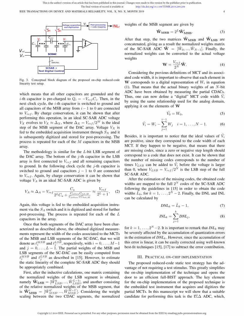
The described reduced-code strategy is the base of the workin [10], [15], where MCT-based measurements are proposedfor binary-weighted SAR ADCs. In this section we extendthis strategy to cope also with generic M × L split-capacitorarrays. The proposed test strategy is conceptually depicted inFig. 3. Firstly, the MCTs of each partial CDAC are measuredindependently. Two test switches, labelled SA and SX , havebeen added to the SC-SAR ADC under test in order to connectthe top plate of the LSB and MSB segments of the capacitor ar-ray to an embedded test instrument (conceptually representedas a voltmeter) that captures and digitizes the partial MCTs.Then, by digital post-processing of the measurement we caninfer the full static characteristic, including INL, DNL anddetection of missing codes in the SC-SAR ADC under test.It is important to note that even though the partial CDACsare being measured separately, the mismatches of the adjacentCDAC and bridge capacitor are taken into account becausetheir equivalent capacitance has influence on the linearity ofeach CDAC segment.
Let us detail the complete test strategy for a genericM×L SC-SAR ADC. Firstly we characterize the M -bit MSBsegment in the following way: initially, switches SX and SA
are opened, and the bottom of the i-th capacitor in the MSBarray is connected to Vref while all the remaining capacitorsare connected to ground. In this first phase, Ssamp = 1,
This is the author's version of an article that has been published in this journal. Changes were made to this version by the publisher prior to publication.The final version of record is available at http://dx.doi.org/10.1109/TDMR.2019.2891298
Copyright (c) 2019 IEEE. Personal use is permitted. For any other purposes, permission must be obtained from the IEEE by emailing [email protected].
IEEE TRANSACTIONS ON DEVICE AND MATERIALS RELIABILITY, VOL. X, NO. X, MONTH 2019 4
Voltage acquisitionand digitization
Post-processing+ code mapping
Fig. 3. Conceptual block diagram of the proposed on-chip reduced-codelinearity test setup.
which means that all other capacitors are grounded and thei-th capacitor is pre-charged to Qi = −VrefCi. Then, in thenext clock cycle, the i-th capacitor is switched to ground andall capacitors of the MSB array from i− 1 to 0 are connectedto Vref . By charge conservation, it can be shown that afterperforming this operation, in an ideal SC-SAR ADC voltageVX evolves to VX ≈ ∆X , where ∆X = Vref/2
M is the idealstep of the MSB segment of the DAC array. Voltage VX isfed to the embedded acquisition instrument through SX and itis subsequently digitized and stored for post-processing. Theprocess is repeated for each of the M capacitors in the MSBarray.
The methodology is similar for the L-bit LSB segment ofthe DAC array. The bottom of the j-th capacitor in the LSBarray is first connected to Vref and all remaining capacitorsto ground. In the following clock cycle the j-th capacitor isswitched to ground and capacitors j − 1 to 0 are connectedto Vref . Again, by charge conservation it can be shown thatvoltage VA in an ideal SC-SAR ADC is given by
VA ≈ ∆A = VrefCu
2LCu +CattenCtot,M
Catten+Ctot,M
≈ Vref2L + 1
, (2)
Again, this voltage is fed to the embedded acquisition instru-ment via the SA switch and it is digitized and stored for furtherpost-processing. The process is repeated for each of the Lcapacitors in the array.
Once that both segments of the DAC array have been char-acterized as described above, the obtained digitized measure-ments represent the width of the codes associated to the MCTsof the MSB and LSB segments of the SC-DAC, that we willdenote as `MSB
i and `LSBj , respectively, with i = 0, . . . ,M−1
and j = 0, . . . , L − 1. The partial weights of the MSB andLSB segments of the SC-DAC can be easily computed from`MSBi and `LSB
j as described in [15]. However, to estimatethe static linearity of the complete SC-SAR ADC they shouldbe appropriately combined.
First, after the inductive calculations, one matrix containingthe normalized weights of the LSB segment is obtained,namely WLSB = [W 0
LSB , ..., WL−1LSB ], and another consisting
of the relative normalized weights of the MSB segment, thatis W′
MSB = [W 0′
MSB , ..., WM−1′
MSB ]. Considering the weightscaling between the two CDAC segments, the normalized
weights of the MSB segment are given by
WMSB = 2LW′MSB. (3)
After that step, the two matrices WMSB and WLSB areconcatenated, giving as a result the normalized weights matrixof the SC-SAR ADC W = [W0, ..., WN−1]. Finally, thenormalized weights can be converted to the actual voltageweights
W =Vref2N
W. (4)
Considering the previous definitions of MCT and its associ-ated code width, it is important to observe that each element inW corresponds to a digital representation of Wi in equation(1). That means that the actual binary weights of an N -bitADC have been obtained by measuring the partial CDACs.Thus, one can now define a “digital” MCT code width Viby using the same relationship used for the analog domain,applying it on the elements of W
V0 = W0, (5)
Vi = Wi −i−1∑j=1
Wj i = 1, . . . , N − 1. (6)
Besides, it is important to notice that the ideal values of Viare positive, since they correspond to the code width of eachMCT. If they happen to be negative, that means that thereare missing codes, since a zero or negative step length shouldcorrespond to a code that does not exist. It can be shown thatthe number of missing codes corresponds to the number oftimes VLSB can be added to Vi before the voltage is largerthan 0, where VLSB = Vref/2
N is the LSB step of the fullSC-SAR ADC.
After the estimation of the missing codes, the obtained codewidths are mapped to the full 2N codes of the SC-SAR ADCfollowing the guidelines in [15] in order to obtain the codewidths Lk, for k = 1, . . . , 2N − 2. Finally, the DNL and INLcan be calculated by
DNLk = Lk − 1, (7)
INLk =k∑
j=1
DNLj , (8)
for k = 1, . . . , 2N−2. It is important to remark that INLk maybe severely affected by the accumulation of quantization errorsin the estimation of DNLk. However, since the accumulation ofthis error is linear, it can be easily corrected using well-knownbest-fit techniques [15], [17] to subtract the error contribution.
III. PRACTICAL ON-CHIP IMPLEMENTATION
The proposed reduced-code static test strategy has the ad-vantage of not requiring a test stimulus. This greatly simplifiesthe on-chip implementation of the technique and opens thedoor to an efficient full-BIST approach. The key elementfor the on-chip implementation of the proposed technique isthe embedded test instrument that acquires and digitizes thepartial MCTs. In this manuscript we will show that a suitablecandidate for performing this task is the IΣ∆ ADC, which,
This is the author's version of an article that has been published in this journal. Changes were made to this version by the publisher prior to publication.The final version of record is available at http://dx.doi.org/10.1109/TDMR.2019.2891298
Copyright (c) 2019 IEEE. Personal use is permitted. For any other purposes, permission must be obtained from the IEEE by emailing [email protected].

IEEE TRANSACTIONS ON DEVICE AND MATERIALS RELIABILITY, VOL. X, NO. X, MONTH 2019 5
1-bitDAC
Reset
2
Vref
Clock
Fig. 4. Conceptual block diagram of an Incremental Σ∆ ADC.
conceptually, is a mix between a dual-slope and a Σ∆ ADC[18]. This topology is suited for measuring DC voltages suchas in digital voltmeters and instrumentation and measurementapplications. On the other hand, oversampling Σ∆ ADCs aremore prone to gain and offset errors, and it has been provedthat the incremental Σ∆ modulation is inherently more robustto complex non-linear effects such as idle tone generation anddead zones [19]. In addition, well-known digital test solutionsfor Σ∆ modulators can be adapted for assuring the correctfunctionality of the added test circuitry [20], [21]. In theremainder of this section, the basic operation of an IΣ∆ ADCis explained and the design trade-offs for sizing the proposedcircuitry are explored. Moreover, we will show that we canmerge the CDAC of the SC-SAR ADC under test with theinput stage of an IΣ∆ ADC by using the same operationprinciple of a multiplying DAC (MDAC) [22], which furtherreduces the overhead and simplifies the implementation.
A. Incremental Σ∆ ADC for reduced-code testing
Fig. 4 shows a conceptual block diagram of a first-orderIΣ∆ ADC. The operation of the IΣ∆ ADC differs from aΣ∆ in which both integrator and counter are reseted at thebeginning of each conversion. Thus, for a given resolutionR, the integration of each input sample is performed for 2R
cycles. The output of the comparator is triggered every timethe integrator output crosses 0, incrementing the counter andsending a logic 1 via the feedback path to be subtracted fromthe converter input. After 2R cycles, it can be shown that [18]
Nout = 2R(
bVinb2Vref
)+ ε, (9)
where b and b2 represent the integrator input and feedbackgains, respectively, and |ε| ≤ 1. Note that since the numberof counts is acquired by a simple digital counter, this result isalready a quantized representation of the input.
Let us consider the operation of the proposed reduced-codetest technique, as depicted in Fig. 3, using a first-order IΣ∆ADC for acquiring and digitizing each MCT measurement. Itcan be shown by developing equation (9) that the digital codelength representations in LSBs of each partial CDAC are givenby
`MSBi ≈ 2M−R
b2bX
Nout,i, (10)
`LSBj ≈ (2L + 1)
2Rb2bANout,j . (11)
where bX and bA represent the input gain of the IΣ∆ ADCwhen the system is configured for measuring the MSB andLSB segments of the CDAC array, respectively. Notice thatthese input gains do not have to be equal, which, as it will beshown later in this paper may have important implications forsimplifying the implementation.
B. System-level design trade-offs
In order to provide some design guidelines for the imple-mentation of the IΣ∆ ADC in the context of the proposedreduced-code static linearity test application, this subsectionexplores the trade-offs between the accuracy in the estimationof static linearity performances and the resolution and fullscale of the IΣ∆ ADC for test. These trade-offs are exploredbased on behavioral simulations performed in Matlab. Realisticbehavioral models of the test setup in Figs. 3 and 4 have beendeveloped following the guidelines in [23].
The first relevant aspect to take into consideration is themeasurement accuracy as a function of the full-scale range ofthe IΣ∆ ADC for test. In this line, in order to simplify theinterpretation of the results, we normalized the full scale ofthe IΣ∆ for the MSB measurement configuration, FSMSB
IΣ∆ =(b2/bX)Vref to the FS of the SC-DAC (i.e., Vref ).
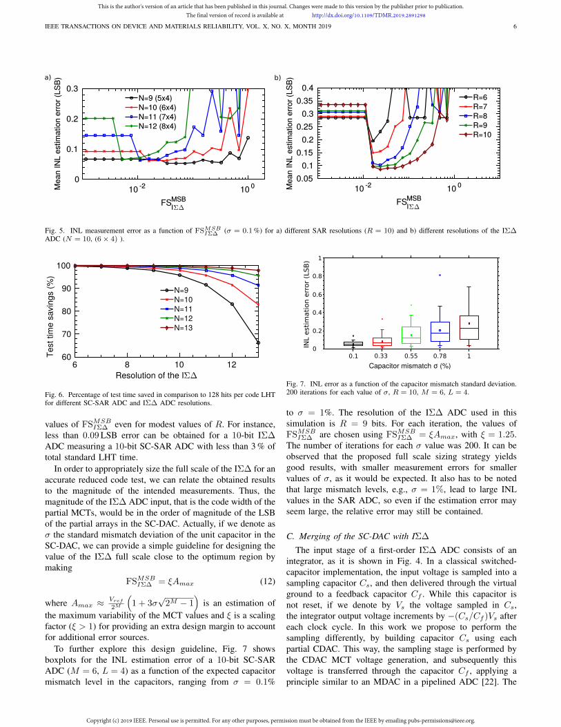
Fig. 5a plots the average INL estimation error as a functionof FSMSB
IΣ∆ using the proposed test methodology for differ-ent SAR ADC resolutions, N . The results are obtained bycalculating the average test error of 250 randomly generatedSC-SAR ADC samples with capacitor mismatch standarddeviation σ = 0.1 % and R = 10. It can be observed thatthe curve presents a zone with high measurement errors inthe lateral extremities of its horizontal axis, and a range ofsmall errors around its center. Not surprisingly, higher SC-SAR ADC resolutions yields higher estimation errors. Again,it is important to stress that each scenario demands only Nmeasurements for deriving the full INL characteristic.
On the other hand, Fig. 5b shows the INL estimation erroras a function of FSMSB
IΣ∆ for different values of the IΣ∆resolution, R. The resolution of the SC-SAR ADC is fixedto N = 10 bits (M = 6 and L = 4) for this experiment. Itcan be observed that there is an optimal range for FSMSB
IΣ∆ ,like the previous case. Nonetheless, for this case there is nosignificant dependence with R for low values of FSMSB
IΣ∆ . Thisis due to the fact that the output of the integrator saturates,which means that taking more samples does not affect theoperation of the circuit [15]. It can also be observed that inthe optimal range, the error is smaller for higher values of R.However, since the test time is given by 3N2R/fs, wherefs is the clock frequency, it is important to pay attentionto the existing trade-off between error and test time, sincethe latter increases exponentially with R. In this line, Fig. 6illustrates the total percentage of time saved in comparison tothe standard Linear Histogram Test (LHT) with 128 hits percode for different values of N . As it can be observed, highsavings in test time can be obtained. Looking at Fig. 5b, it canbe seen that relatively small errors can be obtained for some
This is the author's version of an article that has been published in this journal. Changes were made to this version by the publisher prior to publication.The final version of record is available at http://dx.doi.org/10.1109/TDMR.2019.2891298
Copyright (c) 2019 IEEE. Personal use is permitted. For any other purposes, permission must be obtained from the IEEE by emailing [email protected].
IEEE TRANSACTIONS ON DEVICE AND MATERIALS RELIABILITY, VOL. X, NO. X, MONTH 2019 6
Fig. 5. INL measurement error as a function of FSMSBIΣ∆ (σ = 0.1 %) for a) different SAR resolutions (R = 10) and b) different resolutions of the IΣ∆
ADC (N = 10, (6 × 4) ).
6 8 10 12Resolution of the I
60
70
80
90
100
Test
tim
e sa
ving
s (%
)
N=9N=10N=11N=12N=13
Fig. 6. Percentage of test time saved in comparison to 128 hits per code LHTfor different SC-SAR ADC and IΣ∆ ADC resolutions.
values of FSMSBIΣ∆ even for modest values of R. For instance,
less than 0.09 LSB error can be obtained for a 10-bit IΣ∆ADC measuring a 10-bit SC-SAR ADC with less than 3 % oftotal standard LHT time.
In order to appropriately size the full scale of the IΣ∆ for anaccurate reduced code test, we can relate the obtained resultsto the magnitude of the intended measurements. Thus, themagnitude of the IΣ∆ ADC input, that is the code width of thepartial MCTs, would be in the order of magnitude of the LSBof the partial arrays in the SC-DAC. Actually, if we denote asσ the standard mismatch deviation of the unit capacitor in theSC-DAC, we can provide a simple guideline for designing thevalue of the IΣ∆ full scale close to the optimum region bymaking
FSMSBIΣ∆ = ξAmax (12)
where Amax ≈ Vref
2M
(1 + 3σ
√2M − 1
)is an estimation of
the maximum variability of the MCT values and ξ is a scalingfactor (ξ > 1) for providing an extra design margin to accountfor additional error sources.
To further explore this design guideline, Fig. 7 showsboxplots for the INL estimation error of a 10-bit SC-SARADC (M = 6, L = 4) as a function of the expected capacitormismatch level in the capacitors, ranging from σ = 0.1%
0.1
Capacitor mismatch σ (%)0.33 0.55 0.78 1
0
0.2
0.4
0.6
0.8
1
INL
est
imati
on e
rror
(LSB
)
Fig. 7. INL error as a function of the capacitor mismatch standard deviation.200 iterations for each value of σ, R = 10, M = 6, L = 4.
to σ = 1%. The resolution of the IΣ∆ ADC used in thissimulation is R = 9 bits. For each iteration, the values ofFSMSB
IΣ∆ are chosen using FSMSBIΣ∆ = ξAmax, with ξ = 1.25.
The number of iterations for each σ value was 200. It can beobserved that the proposed full scale sizing strategy yieldsgood results, with smaller measurement errors for smallervalues of σ, as it would be expected. It also has to be notedthat large mismatch levels, e.g., σ = 1%, lead to large INLvalues in the SAR ADC, so even if the estimation error mayseem large, the relative error may still be contained.
C. Merging of the SC-DAC with IΣ∆
The input stage of a first-order IΣ∆ ADC consists of anintegrator, as it is shown in Fig. 4. In a classical switched-capacitor implementation, the input voltage is sampled into asampling capacitor Cs, and then delivered through the virtualground to a feedback capacitor Cf . While this capacitor isnot reset, if we denote by Vs the voltage sampled in Cs,the integrator output voltage increments by −(Cs/Cf )Vs aftereach clock cycle. In this work we propose to perform thesampling differently, by building capacitor Cs using eachpartial CDAC. This way, the sampling stage is performed bythe CDAC MCT voltage generation, and subsequently thisvoltage is transferred through the capacitor Cf , applying aprinciple similar to an MDAC in a pipelined ADC [22]. The
This is the author's version of an article that has been published in this journal. Changes were made to this version by the publisher prior to publication.The final version of record is available at http://dx.doi.org/10.1109/TDMR.2019.2891298
Copyright (c) 2019 IEEE. Personal use is permitted. For any other purposes, permission must be obtained from the IEEE by emailing [email protected].

IEEE TRANSACTIONS ON DEVICE AND MATERIALS RELIABILITY, VOL. X, NO. X, MONTH 2019 7
-
+
Cf
Cout,k
+
-Vi
Sk
-
+
Cf
Cout,k
Sk
+ -bkVi
Fig. 8. Conceptual operation of merging between CDAC and IΣ∆ ADC:first, MCT step length Vi is generated. Then, charge in Cout,k is transferredto Cf via Sk , integrating Vi with gain bk .
main advantages of this approach are that, first, transferringcharge in this manner eliminates the need of a high-impedancebuffer between the CDAC and the input of the IΣ∆ ADC.Second, reusing the CDAC as the sampling capacitor in theIΣ∆ significantly reduces the area overhead of the proposedsolution. Third, as it will be shown subsequently, we have theadditional advantage of scaling the FS of the IΣ∆ ADC inorder to compensate for the expected change in magnitude ofthe MCT voltages for each partial CDAC.
The proposed configuration is conceptually shown in Fig.8. Voltage Vi corresponds to the target MCT to be measured,generated as described in Section II.C. After Sk (k = A forthe LSB segment, k = X for the MSB segment) is connected,the charge stored in the CDAC is transferred to Cf in a waythat the output is incremented by ≈ −Vi×Ctot,k/Cf = bkVi,where bk = −Ctot,k/Cf is the integrator gain.
Taking into consideration the guidelines for sizing ofFSMSB
IΣ∆ derived in the previous subsection, we can size thecapacitors in the integrator. By using the definition of FSMSB
IΣ∆
together with the definition of Amax, it follows that
FSMSBIΣ∆ =
b2bX
Vref =b2Cf
Cout,MSBVref = ξAmax, (13)
where the output capacitance of the MSB array is Cout,MSB ≈2MCu, with Cu being the unitary capacitor of the array.Hence, the optimal value for the integrator feedback capacitorCf,opt can be derived
Cf,opt =ξ
b2Cu
(1 + 3σ
√2M − 1
). (14)
The value of the reference feedback capacitor, CsR,opt, is thensized as
CsR,opt = b2Cf,opt. (15)
The capacitive scaling of the proposed implementationhas the additional advantage of naturally compensating themagnitude difference between the measurements of the MSBand LSB sections of the SC-DAC. Let us consider again theproposed test strategy described in Section II.C in the viewof the proposed implementation. For the measurements ofthe MSB segment, switch SX in Fig. 3 is turned on andthe integrator input gain is given by bX ≈ 2MCu/Cf . Asdiscussed before, for an ideal SC-DAC, the voltage generatedat the node VX when generating the partial MCTs is given by∆X , as defined in the previous section. Conversely, when SA
is on for the measurement of the LSB segment of the SC-DACthe integrator input gain is given by bA ≈ (2L + 1)Cu/Cf ,
while, for an ideal SC-DAC, the voltage generated at node VAis given by ∆A, as defined in the previous section.
If we define r as the ratio between step sizes, we obtain
r =∆X
∆A≈ Vref/2
M
Vref/(2L + 1)=
2L + 1
2M, (16)
but at the same time if we compute the ratio between the inputgains of the integrator in the two configurations
bXbA
=FSLSB
IΣ∆
FSMSBIΣ∆
=Cout,MSB/Cf
Cout,LSB/Cf=
2M
2L + 1=
1
r, (17)
which shows that the FS of the IΣ∆ is scaled in a way thatnaturally compensates the change in magnitude of the expectedvalues of the partial step sizes. The proposed implementationassures that the factor by which these magnitudes change isexactly the value that guarantees that the measurement remainson the optimal range for both the MSB and LSB segments ofthe SC-DAC.
IV. RESULTS
In order to validate the feasibility and performance of theproposed on-chip reduced-code test strategy, we have designeda SC-SAR ADC together with an embedded IΣ∆ converter inSTMicroelectronics 65 nm CMOS technology, following theguidelines discussed in the previous sections. The SC-SARADC under test is a 10-bit (6 × 4) SC-SAR ADC. The unitcapacitor in the SC-DAC array has been designed as a 9 fFMOM capacitor, the circuit is biased at VDD = 1.2 V and itis clocked at fs = 60 MHz. The digital logic controlling theapproximation register and the execution of the test procedurehas been implemented using behavioral VerilogA models tospeed up simulations. Regarding the embedded first-orderIΣ∆ ADC, capacitors have been sized following the designguidelines in the previous section. The integration capacitoris sized as Cf = 11Cu, and the reference feedback capacitoris set to CsR = 4Cu. Relative to the CDAC array in theSAR ADC, these extra capacitors represent an area overheadof about 15%. The resolution of the IΣ∆ ADC has been set toR = 10 bits and the full scale has been adjusted from equation(13) to be about four times the LSB of the partial CDACs.Again, the digital counter has been modeled in VerilogA tospeed up the simulations.
In order to validate the performance of the proposedreduced-code static linearity test strategy, we use the mismatchMonte Carlo models in the Process Design Kit (PDK) of thetechnology to generate samples of the SC-SAR ADC undertest. The worst-case sample in terms of static linearity hasbeen selected and characterized using the proposed reduced-code test strategy and the standard Linearity Histogram Test(LHT) with 128 hits per code by electrical simulation. Theobtained results for DNL and INL estimations are shown inFig. 9a and b, respectively, while the estimation error, definedas the difference of the reduced-code results with respect tothe LHT results, are shown in Fig. 9c and d. As it can beobserved, the test results are very close to each other, withdifferences smaller than 0.06 LSB. With respect to the test timesavings, the proposed reduced-code static test only requires 10
This is the author's version of an article that has been published in this journal. Changes were made to this version by the publisher prior to publication.The final version of record is available at http://dx.doi.org/10.1109/TDMR.2019.2891298
Copyright (c) 2019 IEEE. Personal use is permitted. For any other purposes, permission must be obtained from the IEEE by emailing [email protected].

IEEE TRANSACTIONS ON DEVICE AND MATERIALS RELIABILITY, VOL. X, NO. X, MONTH 2019 8
a) b)
INL
(LSB
)
c)d)
0 200 400 600 800 1000Codes
-0.6-0.4-0.2
00.20.40.6
DN
L (L
SB)
Linear histogramReduced-code
0 200 400 600 800 1000 1200Codes
-0.5
-0.25
0
0.25
0.5
INL
(LSB
)
Linear histogramReduced-code
0 200 400 600 800 1000Codes
-0.05-0.03-0.010.010.030.050.070.09
DN
L es
timat
ion
erro
r (LS
B)
0 200 400 600 800 1000Codes
-0.05
0.05
INL
estim
atio
n er
ror (
LSB)
Fig. 9. Comparison between LHT and reduced-code linearity measurements for circuit implementation of SC-SAR ADC with R = 10 bits (6× 4): a) DNLmeasurements, b) INL measurements, c) DNL estimation difference, and d) INL estimation difference.
measurements, while the LHT has to traverse the complete setof codes of the ADC under test. Neglecting post-processingtime, the reduced-code strategy offers about a 98% test timereduction with respect to a 128-hit-per-code histogram test.
It is important to remark that the novel reduced-code teststrategy in this manuscript also offers test time savings withrespect to our previous work [15]. Thus, the modified SARoperation in [10], [15] required i × 2R cycles for measuringthe code width associated to the i-th MCT, while our novelstrategy requires 3×2R cycles per measurement, independentlyof the capacitor being exercised. For a 10-bit SAR ADC, thisdifference represents test time savings of about 54%.
To further validate the performance of the proposedreduced-code static test technique, another set of experimentswere performed to verify the functionality of the techniquein the presence of missing codes. In these experiments, weartificially increased the mismatch of the capacitors above thetechnological value in the PDK in order to generate missingcodes in the transfer function of the 10-bit SC-SAR ADCunder test. Results are shown in Fig. 10 where we present theDNL characteristic of the SC-SAR ADC under test zoomedaround the area of two missing codes (DNL = −1 LSB),measured both with the proposed reduced-code static teststrategy and with the standard LHT with 128 hits per code.It is clear to see that the proposed reduced-code techniqueaccurately detects the presence of the missing codes.
V. CONCLUSIONS
This work presented a novel reduced-code static linearitytest technique appropriate for Split-Capacitor SAR ADCs. Theproposed test strategy is based on the direct measurement of
500 510 520 530Codes
-1
-0.75
-0.5
-0.25
0
DN
L (L
SB)
Linear histogramReduced-code
Fig. 10. Detection of missing codes.
the code width associated to the Major Carrier Transitions ofeach of the segments of the SC-DAC of the converter undertest. The set of MCTs are directly generated with no need for atest stimulus, which simplifies the practical implementation ofthe technique. It has been shown that the complete static lin-earity characteristic of an N -bit SC-SAR ADC can be inferredwith only N measurements, which may yield significant testtime reductions in the static characterization of this system.
We have provided practical guidelines for the on-chip im-plementation of the proposed reduced-code test technique. Inthis line, it has been shown that the code width associatedto each MCT can be measured with an embedded IΣ∆ ADC.Furthermore, the design of such a converter has been discussedand we have proposed an efficient implementation that reusesthe input SC-DAC as sampling capacitor for the IΣ∆ ADC.
The feasibility and performance of the proposed reduced-code test technique have been validated with behavioral andelectrical simulations of a 10-bit (6×4) SC-SAR ADC imple-
This is the author's version of an article that has been published in this journal. Changes were made to this version by the publisher prior to publication.The final version of record is available at http://dx.doi.org/10.1109/TDMR.2019.2891298
Copyright (c) 2019 IEEE. Personal use is permitted. For any other purposes, permission must be obtained from the IEEE by emailing [email protected].

IEEE TRANSACTIONS ON DEVICE AND MATERIALS RELIABILITY, VOL. X, NO. X, MONTH 2019 9
mented in a 65 nm CMOS technology. Obtained results showthe equivalence of the proposed measurements to standardLinearity Histogram Test methods. INL and DNL estimationerrors were contained to ±0.06 LSB, while test time savingsare in the order of 98% when compared to a 128-hit-per-codehistogram.
Future work in this research will include the fabrication andexperimental validation of the proposed BIST technique andthe estimation of test quality metrics (i.e., test escapes andyield loss).
REFERENCES
[1] P. Harpe, “Ultra-low power analog-digital converters for IoT.” Enablingthe Internet of Things. Springer, Cham, January 2017. 361-383. DOI:10.1007/978-3-319-51482-6 13.
[2] J.-Y. Um, Y. Kim, E. Song, J. Sim, and H. Park, “A digital-domaincalibration of split-capacitor DAC for a differential SAR ADC withoutadditional analog circuits.” IEEE Transactions on Circuits and Systems I:Regular Papers, vol. 60, no. 11, pp. 2845-2856, November 2013. DOI:10.1109/TCSI.2013.2252475.
[3] Y. Chen, X. Zhu, H. Tamura, M. Kibune, Y. Tomita, T. Hamada, M.Yoshioka, K. Ishikawa, T. Takayama, J. Ogawa, S. Tsukamoto, T. Kuroda,“Split capacitor DAC mismatch calibration in successive approxima-tion ADC.” 2009 IEEE Custom Integrated Circuits Conference, Rome,September 2009, pp. 279-282. DOI: 10.1109/CICC.2009.5280859.
[4] F. Poehl, F. Demmerle, J. Alt and H. Obermeir, “Production test chal-lenges for highly integrated mobile phone SOCs—A case study.” 15thIEEE European Test Symposium, Praha, May 2010, pp. 17-22. DOI:10.1109/ETSYM.2010.5512786.
[5] “IEEE Standard for Terminology and Test Methods for Analog-to-DigitalConverters,” IEEE Std 1241-2010 (Revision of IEEE Std 1241-2000), pp.1–139, January 2011. DOI: 10.1109/IEEESTD.2011.5692956.
[6] S. Goyal, A. Chatterjee, M. Atia, H. Iglehart, Chung Yu Chen, B.Shenouda, N. Khouzam, H. Haggag, “Test time reduction of successiveapproximation register A/D converter by selective code measurement.”IEEE International Conference on Test, Austin, TX, November 2005, pp.8 pp.-225. DOI: 10.1109/TEST.2005.1583979.
[7] A. Laraba, H. Stratigopoulos, S. Mir and H. Naudet, “Exploiting pipelineADC properties for a reduced-code linearity test technique.” IEEE Trans-actions on Circuits and Systems I: Regular Papers, vol. 62, no. 10, pp.2391-2400, October 2015. DOI: 10.1109/TCSI.2015.2469014.
[8] E. Peralias, A. Gines, and A. Rueda. “INL systematic reduced-testtechnique for Pipeline ADCs.” 19th IEEE European Test Symposium(ETS), Paderborn, May 2014, pp. 1-6. DOI: 10.1109/ETS.2014.6847818.
[9] T. Chen, X. Jin, R. L. Geiger, and D. Chen, “User-smile: Ultrafaststimulus error removal and segmented model identification of linearityerrors for ADC built-in self-test,” IEEE Transactions on Circuits andSystems I: Regular Papers, vol. 65, no. 7, pp. 2059–2069, July 2018.DOI: 10.1109/TCSI.2017.2775632.
[10] Xuan-Lun Huang, Hung-I Chen, Jiun-Lang Huang, Chang-Yu Chen,Tseng Kuo-Tsai, Ming-Feng Huang, Yung-Fa Chou, Ding-Ming Kwai,“Testing and calibration of SAR ADCs by MCT-based bit weight extrac-tion.” IEEE 18th International Mixed-Signal, Sensors, and Systems TestWorkshop, Taipei, July 2012, pp. 1-4. DOI: 10.1109/IMS3TW.2012.11.
[11] H.-S. Lee, D. A. Hodges, and P. R. Gray. “A self-calibrating 15 bitCMOS A/D converter.” IEEE Journal of Solid-State Circuits, vol. 19,no. 6, pp. 813-819, December 1984. DOI: 10.1109/JSSC.1984.1052231.
[12] M. Yoshioka, K. Ishikawa, T. Takayama and S. Tsukamoto, “A 10-b50-MS/s 820-µ W SAR ADC With On-Chip Digital Calibration.” IEEETransactions on Biomedical Circuits and Systems, vol. 4, no. 6, pp. 410-416, December 2010. DOI: 10.1109/TBCAS.2010.2081362.
[13] A. T. Huynh, H. T. Duong, H. V. Le and E. Skafidas, “Design of a capaci-tive DAC mismatch calibrator for split SAR ADC in 65 nm CMOS.” Asia-Pacific Microwave Conference Proceedings (APMC), Seoul, November2013, pp. 503-505. DOI: 10.1109/APMC.2013.6694845.
[14] H-J. Lin, X-L. Huang, and J-L. Huang, “A mutual characterization basedSAR ADC self-testing technique.” 18th IEEE European Test Symposium(ETS), Avignon, May 2013, pp. 1-6. DOI: 10.1109/ETS.2013.6569365.
[15] R. S. Feitoza, M. J. Barragan, S. Mir and D. Dzahini, “Reduced-code static linearity test of SAR ADCs using a built-in incremental Σ∆converter.” IEEE International Symposium on On-Line Testing and RobustSystem Design (IOLTS). July 2018, pp. 1-6.
[16] G. W. Roberts, F. Taenzler, and M. Burns An introduction to mixed-signal IC test and measurement, 2nd edition. New York, Oxford Univer-sity Press, October 2011.
[17] M. Mahoney, DSP-Based Testing of Analog and Mixed-Signal Circuits.Los Alamitos, CA, USA: IEEE Computer Society Press, May 1987.
[18] J. Markus, J. Silva, and G. C. Temes, “Theory and applications ofincremental ∆Σ converters.” IEEE Transactions on Circuits and SystemsI: Regular Papers, vol. 51, no. 4, pp. 678-690, April 2004. DOI:10.1109/TCSI.2004.826202.
[19] Richard Schreier, Shanthi Pavan, Gabor C. Temes, Understanding delta-sigma data converters, second edition. John Wiley & Sons, January 2017.DOI: 10.1002/9781119258308.
[20] G. Leger and A. Rueda, “Low-Cost Digital Detection of ParametricFaults in Cascaded Σ∆ Modulators,” IEEE Transactions on Circuits andSystems I: Regular Papers, vol. 56, no. 7, pp. 1326-1338, July 2009. DOI:10.1109/TCSI.2008.2006648.
[21] M. J. Barragan, R. Alhakim, H.-G. Stratigopoulos, M. Dubois, S. Mir,H. Le Gall, N. Bhargava, A. Bal, “A Fully-Digital BIST Wrapper Basedon Ternary Test Stimuli for the Dynamic Test of a 40 nm CMOS 18-bitStereo Audio Σ∆ ADC,” IEEE Transactions on Circuits and SystemsI: Regular Papers, vol. 63, no. 11, pp. 1876-1888, Nov. 2016. DOI:10.1109/TCSI.2016.2602387.
[22] B.-S. Song, S.-H. Lee, and M. F. Tompsett, “A 10-b 15-MHz CMOSrecycling two-step A/D converter.” IEEE Journal of Solid-State Circuits,vol. 25, no. 6, pp. 1328-1338, Dec. 1990. DOI: 10.1109/4.62176.
[23] P. Malcovati, S. Brigati, F. Francesconi, F. Maloberti, P. Cusinato andA. Baschirotto, “Behavioral modeling of switched-capacitor sigma-deltamodulators.” IEEE Transactions on Circuits and Systems I: Fundamentaltheory and applications, vol. 50, no. 3, pp. 352-364, March 2003. DOI:10.1109/TCSI.2003.808892.
Renato S. Feitoza (S’16) was born in Santa Cata-rina, Brazil. He received a B.Sc. degree in electronicengineering from the Federal University of SantaCatarina (UFSC), Brazil, in 2014. His M.Sc. degreein electrical engineering was obtained from Pontifi-cal Catholic University of Rio de Janeiro (PUC-Rio)in 2016. He is now pursuing his Ph.D at Grenoble In-stitute of Technology, TIMA laboratory, France. Histhesis focus on test strategies for the developmentof novel reduced-code static linearity test of high-performance Analog-to-Digital converters (ADCs).
He also received the first place award on the student design competitionon Wireless Power Transmission held at the IEEE International MicrowaveSymposium 2017 (IMS2017) at Honolulu (HI).
Manuel J. Barragan (M’14) received a M.Sc.degree in Physics in 2003 and a PhD in Micro-electronics in 2009, both from the University ofSeville, Spain. He is currently a researcher withthe French National Research Council (CNRS) atTIMA Laboratory, France. His research is focusedon the topics of test and design for testability ofanalog, mixed-signal, and RF systems. He currentlyserves in the Technical Program Committee of theDesign, Automation, and Test in Europe (DATE)Conference, IEEE European Test Symposium, and
IEEE VLSI Test Symposium. His PhD research won a Silver Leaf Award atthe IEEE PRIME conference in 2009 and, in 2011, his work was selected forinclusion in the 20th Anniversary Compendium of Most Influential Papersfrom the IEEE Asian Test Symposium. He received the Best Special SessionAward in the 2015 IEEE VLSI Test Symposium and the Best Paper Awardin the 2018 IEEE European Test Symposium.
This is the author's version of an article that has been published in this journal. Changes were made to this version by the publisher prior to publication.The final version of record is available at http://dx.doi.org/10.1109/TDMR.2019.2891298
Copyright (c) 2019 IEEE. Personal use is permitted. For any other purposes, permission must be obtained from the IEEE by emailing [email protected].

IEEE TRANSACTIONS ON DEVICE AND MATERIALS RELIABILITY, VOL. X, NO. X, MONTH 2019 10
Daniel Dzahini graduated from the ”Ecole Centralede Lyon” in France where he defended his PhDin 1991. Then he joined the LPSC laboratory inGrenoble for the ATLAS / LARG collaboration. Heworked on low noise cold preamplifiers in CMOSand GaAs processes, and also on auto-zero low-offset amplifiers. From 2000 up to now, his researchhas been focused on state-of-the-art A/D and D/Aconverters. In 2017, he was awarded in the Frenchinnovation competition ILAB, as leader of the MAS-SAR project. In Dec 2017 he created the start-up
Xdigit, specialized in the design of ADCs for image sensors.
Salvador Mir (M’99) has an Industrial Engineering(Electrical, 1987) degree from the Polytechnic Uni-versity of Catalonia, Barcelona, Spain, and M.Sc.(1989) and Ph.D. (1993) degrees in Computer Sci-ence from the University of Manchester, UK. He isa Research Director of CNRS (Centre National dela Recherche Scientifique) at TIMA Laboratory inGrenoble, France. He is currently director of TIMAand member of the RMS (Reliable Mixed-signalSystems) Group. His research interests are in thefield of mixed-signal/RF/MEMS test.
This is the author's version of an article that has been published in this journal. Changes were made to this version by the publisher prior to publication.The final version of record is available at http://dx.doi.org/10.1109/TDMR.2019.2891298
Copyright (c) 2019 IEEE. Personal use is permitted. For any other purposes, permission must be obtained from the IEEE by emailing [email protected].