2.2mhz, 3a buck or boost converters with an integrated
TRANSCRIPT

General DescriptionThe MAX15036/MAX15037 high-frequency, DC-DC con-verters with an integrated n-channel power MOSFETprovide up to 3A of load current. The MAX15036includes an internal power MOSFET to enable thedesign of a nonsynchronous buck or boost topologypower supply. The MAX15037 is for the design of asynchronous buck topology power supply. Thesedevices operate from a 4.5V to 5.5V or 5.5V to 23Vinput voltage and offer the ability to set the switchingfrequency from 200kHz to 2.2MHz with an externalresistor. The voltage-mode architecture with a peakswitch current-limit scheme provides stable operationup to a 2.2MHz switching frequency. The MAX15036includes a clock output for driving a second DC-DCconverter 180° out-of-phase and a power-on-reset(RESET) output. The MAX15037 includes a power-goodoutput and a synchronous rectifier driver to drive anexternal low-side MOSFET in the buck converter config-uration for high efficiency.
The MAX15036/MAX15037 protect against overcurrentconditions by utilizing a peak current limit as well asovertemperature shutdown providing a very reliableand compact power source for point-of-load regulationapplications. Additional features include synchroniza-tion, internal digital soft-start, and an enable input. TheMAX15036/MAX15037 are available in a thermallyenhanced, space-saving 16-pin TQFN (5mm x 5mm)package and operate over the -40°C to +125°C tem-perature range.
ApplicationsxDSL Modem Power Supplies
Automotive Radio Power Supplies
Servers and Networks
IP Phones/WLAN Access Points
Features 4.5V to 5.5V or 5.5V to 23V Input Voltage Range Output Voltage Adjustable Down to 0.6V (Buck) or
Up to 28V (Boost) 3A Output Current Synchronous Rectifier Driver Output (MAX15037)
for Higher Efficiency Resistor-Programmable Switching Frequency
from 200kHz to 2.2MHz External Synchronization and Enable (On/Off)
Inputs Clock Output for Driving Second Converter 180°
Out-Of-Phase (MAX15036) Integrated 150mΩ High-Side n-Channel Power
MOSFET Power-On-Reset Output (MAX15036)/Power-Good
Output (MAX15037) Short-Circuit Protection (Buck)/Maximum Duty-
Cycle Limit (Boost) Thermal-Shutdown Protection Thermally Enhanced 16-Pin TQFN Package
Dissipates 2.7W
MA
X1
50
36
/MA
X1
50
37
2.2MHz, 3A Buck or Boost Converterswith an Integrated High-Side Switch
________________________________________________________________ Maxim Integrated Products 1
15
16
14
13
6
5
7
DRAI
N FB
8
DRAI
N
PGND
CKO
SOUR
CE
1 2
RESET
4
12 11 9
BST/VDD
EN
VL
V+
BYPASS
OSC
MAX15036
COM
PSG
ND
3
10
SYNC
EP*
*EXPOSED PAD.THIN QFN
5mm x 5mm
TOP VIEW
+
Pin Configurations
Ordering Information
19-4222; Rev 0; 7/08
For pricing delivery, and ordering information please contact Maxim Direct at 1-888-629-4642,or visit Maxim’s website at www.maxim-ic.com.
Pin Configurations continued at end of data sheet.
PART TEMP RANGE PIN-PACKAGE
MAX15036ATE+ -40°C to +125°C 16 TQFN-EP*
MAX15037ATE+ -40°C to +125°C 16 TQFN-EP*
Selector GuidePART CONFIGURATION FEATURES
MAX15036ATENonsynchronous
Buck or BoostRESET Output,Clock Output
MAX15037ATE Synchronous BuckPGOOD Output,Synchronous FET
Driver
+Denotes a lead-free/RoHS-compliant package.*EP = Exposed pad.

MA
X1
50
36
/MA
X1
50
37
2.2MHz, 3A Buck or Boost Converterswith an Integrated High-Side Switch
2 _______________________________________________________________________________________
ABSOLUTE MAXIMUM RATINGS
ELECTRICAL CHARACTERISTICS(V+ = VL = 5V or V+ = 5.5V to 23V, VEN = 5V, TA = TJ = -40°C to +125°C, unless otherwise noted. Circuits of Figures 5 and 6. Typicalvalues are at TA = TJ = +25°C.) (Note 2)
Stresses beyond those listed under “Absolute Maximum Ratings” may cause permanent damage to the device. These are stress ratings only, and functionaloperation of the device at these or any other conditions beyond those indicated in the operational sections of the specifications is not implied. Exposure toabsolute maximum rating conditions for extended periods may affect device reliability.
V+ to PGND............................................................-0.3V to +25VBST/VDD, DRAIN to SGND ....................................-0.3V to +30VSGND to PGND .....................................................-0.3V to +0.3VBST/VDD to SOURCE...............................................-0.3V to +6VSOURCE to SGND..................................................-0.6V to +25VSOURCE or DRAIN Maximum Peak Current...............5A for 1msVL to SGND ................-0.3V to the lower of +6V and (V+ + 0.3V)SYNC, EN, DL, CKO, OSC, COMP,
FB to SGND...............................................-0.3V to (VL + 0.3V)BYPASS, CKO, OSC, COMP, FB, EN, SYNC, RESET,
PGOOD Maximum Input Current .................................±50mARESET, PGOOD to SGND ........................................-0.3V to +6V
BYPASS to SGND..................................................-0.3V to +2.2VVL and BYPASS Short-Circuit Duration to SGND ......ContinuousContinuous Power Dissipation (TA = +70°C)
16-Pin TQFN (derate 33mW/°C above +70°C) ..........2666mWJunction-to-Case Thermal Resistance (θJC) (Note 1)
16-Pin TQFN................................................................1.7°C/WJunction-to-Ambient Thermal Resistance (θJA) (Note 1)
16-Pin TQFN.................................................................30°C/WOperating Temperature Range .........................-40°C to +125°CJunction Temperature Range ............................-65°C to +150°CStorage Temperature Range .............................-65°C to +150°CLead Temperature (soldering, 10s) .................................+300°C
Note 1: Package thermal resistances were obtained using the method described in JEDEC specification JESD51-7, using a four-layerboard. For detailed information on package thermal considerations, refer to http://www.maxim-ic.com/thermal-tutorial.
PARAMETER SYMBOL CONDITIONS MIN TYP MAX UNITS
SYSTEM SPECIFICATIONS
5.5 23.0Input Voltage Range V+
V+ = VL 4.5 5.5V
V+ Operating Supply Current IQV+ = 12V, VFB = 0.8VROSC = 10kΩ, no switching
1.8 2.5 mA
V+ Standby Supply Current ISTBY
V+ = 12V, VEN = 0V, PGOOD(MAX15037), RESET, CKO unconnected(MAX15036), ROSC = 10kΩ
1 1.4 mA
Nonsynchronous (MAX15036),fSW = 1.25MHz, V+ = 12V, IOUT = 1.5A,VOUT = 3.3V
79
Efficiency ηSynchronous (MAX15037),fSW = 300kHz, V+ = 12V, IOUT = 1.5A,VOUT = 3.3V
90
%
VL REGULATOR (VL)/BYPASS OUTPUT (BYPASS)
VL Undervoltage Lockout VUVLO VL falling 4.1 4.3 V
VL Undervoltage LockoutHysteresis
VHYST 137 mV
VL Output Voltage VL V+ = 5.5V to 23V, IVL = 0 to 40mA 5.0 5.2 5.5 V
VL Regulator Short-CircuitCurrent
IVLSHORT VIN = 5.5V 110 mA
BYPASS Output Voltage VBYPASS V+ = VL = 5.2V, IBYPASS = 0 1.98 2 2.02 V
BYPASS Load Regulation ΔVBYPASSIBYPASS steps from 0 to 50μA,V+ = VL = 5.2V
0 1.2 5 mV

MA
X1
50
36
/MA
X1
50
37
2.2MHz, 3A Buck or Boost Converterswith an Integrated High-Side Switch
_______________________________________________________________________________________ 3
ELECTRICAL CHARACTERISTICS (continued)(V+ = VL = 5V or V+ = 5.5V to 23V, VEN = 5V, TA = TJ = -40°C to +125°C, unless otherwise noted. Circuits of Figures 5 and 6. Typicalvalues are at TA = TJ = +25°C.) (Note 2)
PARAMETER SYMBOL CONDITIONS MIN TYP MAX UNITS
SOFT-START
Digital Soft-Start Period Internal 6-bit DAC 4096Clock
periods
Soft-Start Steps 64 Steps
ERROR AMPLIFIER (FB and COMP)
FB to COMP Transconductance gM 1.20 1.8 2.75 mS
FB Input Bias Current IFB 250 nA
FB Input Voltage Set Point VFB 0.591 0.600 0.609 V
COMP Sink-and-Source CurrentCapability
ICOMP 100 150 μA
INTERNAL MOSFETs
On-Resistance n-Channel PowerMOSFET
RON V+ = VL = 5.2V, ISINK = 100mA 0.150 0.302 Ω
Leakage Current ILEAKVEN = 0V, VDRAIN = 23V,SOURCE = PGND
20 μA
Minimum Output Current IOUT VOUT = 3.3V, V+ = 12V (Note 3) 3 A
Peak Current Limit ILIMIT 3.56 4.6 5.6 A
On-Resistance Internal Low-SideSwitch
RONLSW ISWITCH = 50mA, V+ = VL = 5.2V 20 40 Ω
SYNCHRONOUS RECTIFIER DRIVER (DL) (MAX15037 Only)
On-Resistance nMOS RONDLN ISINK = 10mA 1 4 ΩOn-Resistance pMOS RONDLP ISOURCE = 10mA 1.9 5 ΩPeak Sink Current IIDL_SINK 1 A
Peak Source Current IIDL_SOURCE 0.75 A
CLOCK OUTPUT (CKO) (MAX15036 Only)
Clock Output-High Level VCKOH VL = 5.2V, ISOURCE = 5mA 3.54 V
Clock Output-Low Level VCKOL VL = 5.2V, ISINK = 5mA 0.4 V
Clock Output Phase Delay WithRespect to SOURCE Waveform
CKOPHASEROSC = 10kΩ, SYNC = GND(Note 4)
115 Degrees
OSCILLATOR (OSC)/SYNCHRONIZATION (SYNC)
ROSC = 5.62kΩ 2100
ROSC = 41.2kΩ 312Switching Frequency fSW V+ = VL = 5.2V
ROSC = 10kΩ 1130 1250 1380
kHz
Minimum Controllable On-Time tON_MIN 120 ns
Maximum Duty Cycle DMAX fSW = 2.2MHz 82 87.5 %

MA
X1
50
36
/MA
X1
50
37
2.2MHz, 3A Buck or Boost Converterswith an Integrated High-Side Switch
4 _______________________________________________________________________________________
ELECTRICAL CHARACTERISTICS (continued)(V+ = VL = 5V or V+ = 5.5V to 23V, VEN = 5V, TA = TJ = -40°C to +125°C, unless otherwise noted. Circuits of Figures 5 and 6. Typicalvalues are at TA = TJ = +25°C.) (Note 2)
PARAMETER SYMBOL CONDITIONS MIN TYP MAX UNITS
SYNC Frequency Range (Note 5) 200 2200 kHz
SYNC Input to SOURCE Rising-Edge Phase Delay
SYNCPHASEROSC = 10kΩ, fSYNC = 1.2MHz(Note 6)
65 Degrees
SYNC High Threshold VSYNCH 2.0 V
SYNC Low Threshold VSYNCL 0.8 V
SYNC Input Bias Current ISYNC 250 nA
Minimum SYNC High Pulse Width tSYNC_H 100 ns
EN, RESET (MAX15036)/PGOOD (MAX15037)
VIH 2.0EN Threshold
VIL 0.8V
EN Input Bias Current IEN 250 nA
RESET Threshold VTH VFB = VOUT (Note 7) 90 92.5 95 % VOUT
PGOOD Threshold VTH VFB = VOUT (Note 7) 90 92.5 95 % VOUT
FB to RESET or FB to PGOODPropagation Delay
tFD 3 μs
RESET Active Timeout Period tRP 140 200 254 ms
RESET, PGOOD Output VoltageLow
VOL ISINK = 3mA 0.4 V
RESET, PGOOD Output LeakageCurrent
ILEAKV+ = VL = 5.2V, V R ESET orVPGOOD = 6V, VFB = 0.8V
2 μA
THERMAL SHUTDOWN
Thermal Shutdown TSHDN Temperature rising +170 °C
Thermal-Shutdown Hysteresis 25 °C
Note 2: 100% tested at TA = +25°C and TA = +125°C. Limits from TA = -40°C to +25°C are guaranteed by design.Note 3: Output current may be limited by the power dissipation of the package. See the Power Dissipation section in the Applications
Information section.Note 4: From the rising edge of the SOURCE waveform to the rising edge of the CKO waveform.Note 5: SYNC input frequency is equal to the switching frequency.Note 6: From the SYNC rising edge to SOURCE rising edge.Note 7: RESET goes high 200ms after VOUT crosses this threshold, PGOOD goes high after VOUT crosses this threshold.

MA
X1
50
36
/MA
X1
50
37
2.2MHz, 3A Buck or Boost Converterswith an Integrated High-Side Switch
_______________________________________________________________________________________ 5
MAX15036 BUCK EFFICIENCY vs. OUTPUTCURRENT (VIN = 5.5V, fSW = 2.2MHz)
MAX
1503
6 to
c01
OUTPUT CURRENT (A)
EFFI
CIEN
CY (%
)
2.01.51.00.5
10
20
30
40
50
60
70
80
90
00 3.02.5
VOUT = 2.5V
VOUT = 3.3V
MAX15036 BUCK EFFICIENCY vs. OUTPUTCURRENT (VIN = 12V, fSW = 2.2MHz)
MAX
1503
6 to
c02
OUTPUT CURRENT (A)
EFFI
CIEN
CY (%
)
10
20
30
40
60
50
70
80
0
VOUT = 2.5V
VOUT = 3.3V
2.01.51.00.50 3.02.5
MAX15036 BUCK EFFICIENCY vs. OUTPUTCURRENT (VIN = 16V, fSW = 2.2MHz)
MAX
1503
6 to
c03
OUTPUT CURRENT (A)
EFFI
CIEN
CY (%
)
10
20
30
40
50
60
70
02.01.51.00.50 3.02.5
VOUT = 2.5V
VOUT = 3.3V
MAX15037 SYNCHRONOUSEFFICIENCY vs. OUTPUT CURRENT (VIN = 12V, fSW = 330kHz, L = 15μH)
MAX
1503
6 to
c04
OUTPUT CURRENT (A)
EFFI
CIEN
CY (%
)
55
60
65
70
75
80
85
90
95
50L = TOKO DS126C2-150M
2.01.51.00.50 3.02.5
VOUT = 2.5V
VOUT = 3.3V
VOUT = 1.2V
MAX15037 SYNCHRONOUS EFFICIENCY vs. OUTPUT CURRENT (VIN = 12V, fSW = 2.2MHz, L = 4.7μH)
MAX
1503
6 to
c05
OUTPUT CURRENT (A)
EFFI
CIEN
CY (%
)
10
20
30
40
50
60
70
80
02.01.51.00.50 3.02.5
VOUT = 3.3V
MAX15037 OUTPUT VOLTAGE vs. OUTPUTCURRENT (VIN = 12V, VOUT = 3.3V, fSW = 2.2MHz)
MAX
1503
6 to
c06
OUTPUT CURRENT (A)
OUTP
UT V
OLTA
GE (V
)
3.02.51.5 2.01.00.5
3.294
3.295
3.296
3.297
3.298
3.299
3.300
3.301
3.292
3.293
0
VL OUTPUT VOLTAGEvs. SWITCHING FREQUENCY
MAX
1503
6 to
c07
SWITCHING FREQUENCY (kHz)
V L (V
)
21001600600 1100
5.155
5.160
5.165
5.170
5.180
5.175
5.185
5.190
5.150100
VIN = 23V
VIN = 5.5V
Typical Operating Characteristics(V+ = VL = 5.2V, TA = +25°C, Figures 5 and 6, unless otherwise noted.)

MA
X1
50
36
/MA
X1
50
37
2.2MHz, 3A Buck or Boost Converterswith an Integrated High-Side Switch
6 _______________________________________________________________________________________
Typical Operating Characteristics (continued)(V+ = VL = 5.2V, TA = +25°C, Figures 5 and 6, unless otherwise noted.)
MAX15037 VL DROPOUT VOLTAGEvs. SWITCHING FREQUENCY
MAX
1503
6 to
c08
SWITCHING FREQUENCY (kHz)
V L D
ROPO
UT V
OLTA
GE (V
)
21001600600 1100
0.05
0.10
0.15
0.20
0.30
0.25
0.35
0.40
0100
V+ = 5.5V
V+ = 5.25V
V+ = 5V
SWITCHING FREQUENCYvs. ROSC
MAX
1503
6 to
c09
RESISTANCE (kΩ)
FREQ
UENC
Y (k
Hz)
605040302010
1000
10,000
1000 70
SWITCHING FREQUENCYvs. TEMPERATURE
MAX
1503
6 to
c10
TEMPERATURE (°C)
FREQ
UENC
Y (k
Hz)
1106010
350
600
850
1100
1350
1600
1850
2100
2350
100-40
ROSC = 20kΩ
ROSC = 40kΩ
ROSC = 10kΩ
ROSC = 6.04kΩ
MAX15037 LINE-TRANSIENT RESPONSE(IOUT = 1A, VIN STEP = 14V TO 21V)
MAX15036 toc11
100μs/div
VIN 5V/div
0V
200mV/divVOUT
VOUT = 3.3V
MAX15037 LOAD-TRANSIENT RESPONSE (IOUT = 0.5A TO 3A)
MAX15036 toc13
20μs/div
VOUT 200mV/div
0A
1A/divIOUT
VIN = 12VVOUT = 3.3V
MAX15037 LOAD-TRANSIENT RESPONSE(IOUT = 0.2A TO 1A)
MAX15036 toc12
20μs/div
VOUT 100mV/div
0A
500mA/divIOUT
VIN = 12VVOUT = 3.3V
MAX15037 SOFT-START AND SHUTDOWN(NO LOAD)
MAX15036 toc14
1ms/div
VOUT 1V/div
0V
0V
5V/divVEN
VIN = 12V

MA
X1
50
36
/MA
X1
50
37
2.2MHz, 3A Buck or Boost Converterswith an Integrated High-Side Switch
_______________________________________________________________________________________ 7
Typical Operating Characteristics (continued)(V+ = VL = 5.2V, TA = +25°C, Figures 5 and 6, unless otherwise noted.)
MAX15037 SOFT-START AND SHUTDOWN(IOUT = 2A)
MAX15036 toc15
1ms/div
VOUT 1V/div
0V
0V
5V/divVEN
VIN = 12V
VIN STARTUP WAVEFORM(EN CONNECTED TO VL) (MAX15037)
MAX15036 toc16
1ms/div
VEN5V/div
VOUT2V/div
VPGOOD5V/div
VIN10V/div
RESET TIMEOUT(MAX15036)
MAX15036 toc17
40ms/div
10V/divVIN
VEN
VOUT
VRESET
5V/div
5V/div
2V/div
MAX15036 EXTERNALLY SYNCHRONIZED SWITCHING WAVEFORM
MAX15036 toc18
100ns/div
5V/div
5V/div
5V/div
0V
0V
0V
0V
VSYNC
VCKO
VSOURCE_MASTER
VSOURCE_SLAVE5V/div
STANDBY CURRENTvs. TEMPERATURE
MAX
1503
6 to
c19
TEMPERATURE (°C)
STAN
DBY
CURR
ENT
(mA)
100 12060 8020 400
1.45
1.50
1.55
1.60
1.40-40 -20
fSW = 2.2MHzROSC = 5.62kΩ
SWITCHING SUPPLY CURRENT (ISW)vs. TEMPERATURE
MAX
1503
6 to
c20
TEMPERATURE (°C)
SWIT
CHIN
G SU
PPLY
CUR
RENT
(mA)
10075-25 0 25 50
10
20
30
40
50
60
70
80
0-50 125
MAX15036VOUT = 3.3VIOUT = 1AfSYNC = 2.2MHz
fSYNC = 1.2MHz
fSYNC = 600kHz
fSYNC = 300kHz
MAXIMUM OUTPUT CURRENTvs. TEMPERATURE
MAX
1503
6 to
c21
TEMPERATURE (°C)
MAX
IMUM
OUT
PUT
CURR
ENT
(A)
60 11010
3.30
3.40
3.50
3.55
3.60
3.65
3.70
3.75
3.25
3.35
3.45
-40
VIN = 12VVOUT = 3.3VfSW = 1MHz

MA
X1
50
36
/MA
X1
50
37
2.2MHz, 3A Buck or Boost Converterswith an Integrated High-Side Switch
8 _______________________________________________________________________________________
Pin Description
PIN NAME FUNCTION
1, 2 DRAINInternal Power MOSFET Drain Connection. Buck converter operation—use the MOSFET as a high-side switchand connect DRAIN to the input supply. Boost converter operation (MAX15036 only)—use the MOSFET as alow-side switch and connect DRAIN to the inductor and diode junction.
3 COMPTransconductance Error Amplifier Output. Connect a compensation network from COMP to SGND or fromCOMP to FB to SGND (see the Compensation section).
4 FB Feedback Input. Connect a resistive divider from the output to FB to SGND to set the output voltage.
5 OSCSwitching Frequency Set Input. Connect a resistor ROSC from OSC to SGND to set the switching frequency.When using external synchronization, program ROSC so that (0.8 x fSYNC) ≤ fSW ≤ (1.2 x fSYNC). ROSC is stillrequired when external synchronization is used.
6 BYPASS Reference Bypass Connection. Bypass to SGND with a 0.22μF or greater ceramic capacitor.
7 V+Input Supply Voltage. V+ can range from 5.5V to 23V. Connect V+ and VL together for 4.5V to 5.5V inputoperation. Bypass V+ to SGND with a minimum of 0.1μF ceramic capacitor.
8 VLInternal Regulator Output. Bypass VL to SGND with a 4.7μF ceramic capacitor and to PGND with a 0.1μFceramic capacitor. Connect V+ to VL for 4.5V to 5.5V operation.
CKOClock Output (MAX15036 Only). CKO is an output with the same frequency as the converter’s switchingfrequency and 115° out-of-phase. CKO is used to synchronize the MAX15036 to other MAX15036/MAX15037s.
9
DLLow-Side Synchronous Rectifier Driver (MAX15037 Only). DL sources 0.7A and sinks 1A to quickly turn on andoff the external synchronous rectifier MOSFET.
10 SGND Signal Ground
11 PGNDPower Ground. Connect the rectifier diode’s anode, the input capacitor negative terminal, the output capacitornegative terminal, and VL bypass capacitor negative terminal to PGND.
12 SOURCEInternal Power MOSFET Source Connection. Buck converter operation—connect SOURCE to the switched sideof the inductor as shown in Figure 5. Boost converter operation (MAX15036 only)—connect SOURCE to PGND.
13 SYNCExternal Synchronization Input. Connect SYNC to an external logic-level clock to synchronize the MAX15036/MAX15037. Connect SYNC to SGND when not used.
RESETOpen-Drain Active-Low Reset Output (MAX15036 Only). RESET remains low while the converter’s output isbelow 92.5% of VOUT’s nominal set point. When VOUT rises above 92.5% of its nominal set point, RESET goeshigh after the reset timeout period of 200ms (typ).14
PGOODOpen-Drain Power-Good Output (MAX15037 Only). PGOOD remains low while the output is below 92.5% of itsnominal set point.
15 BST/VDD
Internal MOSFET Driver Supply Input. Buck converter operation—bootstrap flying capacitor connection.Connect BST/VDD to an external ceramic capacitor and diode (see Figure 5). Boost converter operation(MAX15036 only)—driver bypass capacitor connection. Connect a low-ESR 0.1μF ceramic capacitor fromBST/VDD to PGND.
16 ENEnable Input. A logic-low turns off the converter. A logic-high turns on the device. Connect EN to VL for analways-on application.
— EP Exposed Pad. Connect to SGND. Solder EP to SGND to enhance thermal dissipation.

MA
X1
50
36
/MA
X1
50
37
2.2MHz, 3A Buck or Boost Converterswith an Integrated High-Side Switch
_______________________________________________________________________________________ 9
LDO
OSCILLATOR
V+
DRAIN
SYNC
2V
1VQ
R
4-PULSESKIP
RSENSECURRENT-LIMIT COMPARATOR
VREF = 0.6V
0.925 x VREF
200mV
200msDELAY
VL = 5.2V
BST/VDD
VL
SOURCE
PGND
FB
COMP
RESET
Q
ADAPTIVEBBM
PWMCOMPARATOR
N2
150mΩ
20Ω
N3
gm
fSW/4
N1
CKO
OSC
BYPASS
EN DIGITALSOFT-START
VREF
MAX15036
SGND
Figure 1. MAX15036 Block Diagram

MA
X1
50
36
/MA
X1
50
37
2.2MHz, 3A Buck or Boost Converterswith an Integrated High-Side Switch
10 ______________________________________________________________________________________
LDO
OSCILLATOR
V+
DRAIN
SYNC
2V
1VQ
R
4-PULSESKIP
RSENSE
VREF = 0.6V
0.925 x VREF
200mV
VL = 5.2V
BST/VDD
VL
SOURCE
PGND
DLVL
FB
COMP
PGOOD
Q
ADAPTIVEBBM
N2
150mΩ
20Ω
N3
gm
fSW/4
N1
OSC
BYPASS
EN DIGITALSOFT-START
VREF
MAX15037
SGND
CURRENT-LIMIT COMPARATOR
PWMCOMPARATOR
Figure 2. MAX15037 Block Diagram

MA
X1
50
36
/MA
X1
50
37
2.2MHz, 3A Buck or Boost Converterswith an Integrated High-Side Switch
______________________________________________________________________________________ 11
Detailed DescriptionPWM Controller
The MAX15036/MAX15037 use a pulse-width modula-tion (PWM) voltage-mode control scheme. TheMAX15036 is a nonsynchronous converter and uses anexternal low-forward-drop Schottky diode for rectifica-tion. The MAX15037 is a synchronous converter anddrives a low-side, low-gate-charge MOSFET for higherefficiency. The controller generates the clock signalfrom an internal oscillator or the SYNC input when dri-ven by an external clock. An internal transconductanceerror amplifier produces an integrated error voltage atCOMP, providing high DC accuracy. The voltage atCOMP sets the duty cycle using a PWM comparatorand an internal 1VP-P voltage ramp. At each risingedge of the clock, the converter’s high-side n-channelMOSFET turns on and remains on until either theappropriate or maximum duty cycle is reached or themaximum current limit for the switch is detected.
In the case of the MAX15036 boost operation, theMOSFET is a low-side switch. During each on-time, theinductor current ramps up. During the second half ofthe switching cycle, the low-side switch turns off andforward biases the Schottky diode. During this time, theDRAIN voltage is clamped to 0.4V (VD) above VOUTand the inductor provides energy to the output as wellas replenishes the output capacitor charge.
MAX15036During each high-side MOSFET on-time (Figure 5), theinductor current ramps up. During the second half of theswitching cycle, the high-side MOSFET turns off and for-ward biases the Schottky rectifier (D2 in Figure 5). Duringthis time, the SOURCE voltage is clamped to 0.5V belowground. The inductor releases the stored energy as itscurrent ramps down, and provides current to the output.During the MOSFET off-time, when the Schottky rectifier isconducting, the bootstrap capacitor (C10 in Figure 5) isrecharged from the VL output. At light loads, theMAX15036 goes in to discontinuous conduction modeoperation when the inductor current completely dis-charges before the next switching cycle commences.When the MAX15036 operates in discontinuous conduc-tion, the bootstrap capacitor can become undercharged.To prevent this, an internal low-side 20Ω switch (see N3 inFigure 1) turns on, during the off-time, once every 4 clockcycles. This ensures that the negative terminal of the boot-strap capacitor is pulled to PGND often enough to allow itto fully charge to VL, ensuring the internal power switchproperly turns on. The operation of the bootstrap capaci-tor wake-up switch causes a small increase in the outputvoltage ripple at light loads. Under overload conditions,
when the inductor current exceeds the peak current limitof the internal switch, the high-side MOSFET turns offquickly and waits until the next clock cycle.
MAX15037The MAX15037 is intended for synchronous buck oper-ation only. During the high-side MOSFET on-time, theinductor current ramps up. When the MOSFET turns off,the inductor reverses polarity and forward biases theSchottky rectifier in parallel with the low-side synchro-nous MOSFET. The SOURCE voltage is clamped to0.5V below ground until the break-before-make time(tBBM) of 25ns is over. After tBBM, the synchronous rec-tifier MOSFET turns on. The inductor releases thestored energy as its current ramps down, and contin-ues providing current to the output. The bootstrapcapacitor is also recharged from the VL output whenthe MOSFET turns off. The synchronous rectifier keepsthe circuit in continuous conduction mode operationeven at light load. Under overload conditions, when theinductor current exceeds the peak current limit of theinternal switch, the high-side MOSFET turns off andwaits until the next clock cycle.
The MAX15037, with the synchronous rectifier driver out-put (DL), has an adaptive break-before-make circuit toavoid cross conduction between the internal power MOSFET and the external synchronous rectifier MOSFET.When the synchronous rectifier MOSFET is turning off, theinternal high-side power MOSFET is kept off until VDL fallsbelow 0.97V. Similarly, DL does not go high until the inter-nal power MOSFET gate voltage falls below 1.24V.
Input Voltage (V+)/Internal LinearRegulator (VL)
All internal control circuitry operates from an internally reg-ulated nominal voltage of 5.2V (VL). At higher input volt-ages (V+) of 5.5V to 23V, VL is regulated to 5.2V. At 5.5Vor below, the internal linear regulator operates in dropoutmode, where VL follows V+. Depending on the load on VL,the dropout voltage can be high enough to reduce VL tobelow the undervoltage lockout (UVLO) threshold.
For input voltages of lower than 5.5V, connect V+ andVL together. The load on VL is proportional to theswitching frequency of the converter. See the VLOutput Voltage vs. Switching Frequency graph in theTypical Operating Characteristics. For an input voltagehigher than 5.5V, use the internal regulator.
Bypass V+ to SGND with a low-ESR 0.1μF or greaterceramic capacitor placed as close as possible to theMAX15036/MAX15037. Current spikes from VL disturbthe internal circuitry powered by VL. Bypass VL with alow-ESR 0.1μF ceramic capacitor to PGND and a low-ESR 4.7μF ceramic capacitor to SGND.

MA
X1
50
36
/MA
X1
50
37 Enable
EN is an active-high input that turns the MAX15036/MAX15037 on and off. EN is a TTL-logic input with 2.0Vand 0.8V logic-high and low levels, respectively. WhenEN is asserted high, the internal digital soft-start cycleslowly ramps up the internal reference and providessome soft-start at the output. Hysteresis provides immu-nity to the glitches during logic turn-on of the converter.Large voltage variations at EN can interrupt the soft-startsequence and can cause a latch-up. Ensure that ENremains high for at least 5ms once it is asserted. ForceEN low to turn off the internal power MOSFET and causeRESET to go low (MAX15036) or cause PGOOD to golow (MAX15037). Connect EN to VL when not used.
Soft-Start/Soft-StopThe MAX15036/MAX15037 include UVLO with hystere-sis to prevent chattering during startup. The UVLO cir-cuit holds the MAX15036/MAX15037 off until V+reaches 4.5V and turns the devices off when V+ fallsbelow 4.3V. The MAX15036/MAX15037 also offer asoft-start feature that reduces surge currents andglitches on the input during turn-on. During turn-onwhen the UVLO threshold is reached or EN goes fromlow to high, the digital soft-start ramps up the reference(VBYPASS) in 64 steps. During a turn-off (by driving ENor V+ low), the reference is reduced to zero slowly. Thesoft-start and soft-stop periods (tSS) are 4096 cycles ofthe internal oscillator. To calculate the soft-start/soft-stopperiod use the following equation:
fSW is the switching frequency of the converter.
Oscillator/Synchronization (SYNC)/Clock Output (CLKOUT)
The clock frequency (or switching frequency) is gener-ated internally and is adjustable through an externalresistor connected from OSC to SGND. The relationshipbetween ROSC and fSW is:
The adjustment range for fSW is from 200kHz to2.2MHz.
Connect a logic-level clock between 200kHz to 2.2MHzat SYNC to externally synchronize the MAX15036/MAX15037’s oscillator (see Figure 8). The MAX15036/MAX15037 synchronize to the rising edge of the SYNCclock. The rising edge of the SYNC clock corresponds to
the turn-on edge of the internal n-channel power MOSFETwith a fixed propagation delay. When operating theMAX15036/MAX15037 with an external SYNC clock,ROSC must be installed. Program the internal switchingfrequency so that (0.8 x fSYNC) ≤ fSW ≤ (1.2 x fSYNC). Theminimum pulse width for fSYNC is 100ns. Connect SYNCto SGND if synchronization is not used.
The CKO output (MAX15036 only) is a logic-level clockwith the same frequency as fSW and with 115° phaseshift with respect to SYNC clock. Two MAX15036s canbe connected in a master/slave configuration for two-phase (180°) interleaved operation. The CKO output ofthe master drives the SYNC input of the slave to form adual-phase converter. To achieve the 180° out-of-phaseoperation, program the internal switching frequency ofboth converters close to each other by using the sameROSC value. When synchronizing the master-slave con-figuration using external clock, program the internalswitching frequency using ROSC close to the externalclock frequency (fSYNC) for 180° ripple phase operation(see Figure 8). Any difference in the internal switchingfrequency and fSYNC changes the phase delay. If bothmaster and slave converters use the same powersource, and share input bypass capacitors, the effec-tive switching frequency at the input is twice the switch-ing frequency of the individual converter. Higher ripplefrequency at the input capacitor means a lower RMSripple current into the capacitor.
Current LimitThe MAX15036/MAX15037 protect against output over-load and short-circuit conditions when operated in abuck configuration. An internal current-sensing stagedevelops a voltage proportional to the instantaneousswitch current. When the switch current reaches 4.6A(typ), the power MOSFET turns off and remains off untilthe next on cycle.
During a severe overload or short-circuit condition whenthe output voltage is pulled to ground, the dischargingslope of the inductor is VDS (the voltage across the syn-chronous FET), or VF (the voltage across the rectifyingdiode) divided by L. The short off-time does not allowthe current to properly ramp down in the inductor, caus-ing a dangerous current runaway and possibly destruc-tion of the device. To prevent this, the MAX15036/MAX15037 include a frequency foldback feature. Whenthe current limit is detected the frequency is reduced to1/4th of the programmed switching frequency. When theoutput voltage falls below 1/3rd of its nominal set point(VFB = 0.2V), the converter is turned off and soft-startcycle is initiated. This reduces the RMS current sourcedby the converter during the fault condition.
Rs
fOSCSW
= ×125 108 Ω /
tfSSSW
= 4096
2.2MHz, 3A Buck or Boost Converterswith an Integrated High-Side Switch
12 ______________________________________________________________________________________

At high input-to-output differential, and high switchingfrequency, the on-time drops to the order of 100ns.Even though the MAX15036/MAX15037 can control theon-time as low as 100ns, the internal current-limit circuitmay not detect the overcurrent within this time. In thatcase, the output current during the fault may exceed thecurrent limit specified in the Electrical Characteristicstable. The MAX15036/MAX15037 may still be protectedagainst the output short-circuit fault through the overtemperature shutdown. However, the output switchcurrent may be as high as 5.6A. If the minimum on-timefor a given frequency and duty cycle is less than200ns, choose the inductor with a saturation current ofgreater than 5.6A.
Power-On Reset (RESET) (MAX15036 Only)
RESET is an active-low open-drain output that goes lowwhen VOUT falls below 92.5% of its nominal set point.RESET goes high impedance when VOUT rises above92.5% of its nominal set point, the soft-start period iscomplete, and the 200ms (typ) timeout period haselapsed. Connect a pullup resistor from RESET to alogic voltage or to VL. The internal open-drain MOSFETat RESET can sink 3mA while providing a TTL-compati-ble logic-low signal. Connect RESET to SGND or leaveunconnected when not used.
Power-Good (PGOOD) (MAX15037 Only)
PGOOD is an open-drain, active-high output that goeslow when VOUT is below 92.5% of its nominal set pointand goes high impedance when VOUT goes above92.5% its nominal set point. Connect a pullup resistorfrom PGOOD to a logic voltage or to VL. PGOOD can sinkup to 3mA while still providing a TTL-compatible logic-lowoutput. Pulling EN low forces PGOOD low. ConnectPGOOD to SGND or leave unconnected when not used.
Thermal-Overload ProtectionDuring a continuous output short-circuit or overloadcondition, the die junction temperature in theMAX15036/MAX15037 can exceed its l imit. TheMAX15036/MAX15037 provide an internal thermal shut-down to turn off the device when the die temperature
reaches +170°C. A thermal sensor monitors the dietemperature and turns the device on again when thetemperature reduces by +25°C. During thermal shut-down, the internal power MOSFET shuts off, DL pulls toSGND, VL shuts down, RESET (MAX15036)/PGOOD(MAX15037) goes low, and soft-start resets.
Applications InformationSetting the Switching Frequency
The controller generates the switching frequency (fSW)through the internal oscillator or the signal at SYNC(fSYNC), when driven by an external oscillator. Theswitching frequency is equal to fSW or fSYNC.
A resistor, ROSC, from OSC to SGND sets the internaloscillator. The relationship between fSW and ROSC is:
where fSW is in Hertz, and ROSC is in ohms. For exam-ple, a 1.25MHz switching frequency is set with ROSC =10kΩ. Higher frequencies allow designs with lowerinductor values and less output capacitance.Consequently, peak currents and I2R losses are lowerat higher switching frequencies, but core losses, gate-charge currents, and switching losses increase.
Rising clock edges on SYNC are interpreted as a syn-chronization input. If the SYNC signal is lost, the internaloscillator takes control of the switching rate, returningthe switching frequency to that set by ROSC. This main-tains output regulation even with intermittent SYNC sig-nals. When using an external synchronization signal, setROSC so that (0.8 x fSYNC) ≤ fSW ≤ (1.2 x fSYNC).
Buck ConverterUse the internal n-channel power MOSFET as a high-side switch to configure the MAX15036/MAX15037 as abuck converter. In this configuration, SOURCE is con-nected to the inductor, DRAIN is connected to theinput, and BST/VDD connects to the cathode of thebootstrap diode and capacitor. Figures 5 and 6 showthe typical application circuits for MAX15036/MAX15037, respectively, in a buck configuration.
R125 10
fOSC
8
SW= ×
MA
X1
50
36
/MA
X1
50
37
2.2MHz, 3A Buck or Boost Converterswith an Integrated High-Side Switch
______________________________________________________________________________________ 13

MA
X1
50
36
/MA
X1
50
37 Effective Input Voltage Range
The MAX15036/MAX15037 can operate with input sup-plies ranging from 4.5V to 5.5V or 5.5V to 23V. Theinput voltage range (V+) can be constrained to a mini-mum by the duty-cycle limitations and to a maximum bythe on-time limitation. The minimum input voltage isdetermined by:
DMAX is the maximum duty cycle of 87.5% (typ).VDROP1 is the total drop in the inductor discharge paththat includes the diode’s forward voltage drop (or thedrop across the synchronous rectifier MOSFET), andthe drops across the series resistance of the inductorand PCB traces. VDROP2 is the total drop in the induc-tors charging path, which includes the drop across theinternal power MOSFET, and the drops across theseries resistance of the inductor and PCB traces.
The maximum input voltage can be determined by:
where tON_MIN = 100ns and fSW is the switching frequency.
Setting the Output VoltageFor 0.6V or greater output voltages, connect a resistivedivider from VOUT to FB to SGND. Select the FB toSGND resistor (R2) from 1kΩ to 10kΩ and calculate theresistor from OUT to FB (R1) by the following equation:
where VFB = 0.6V, see Figure 3.
For designs that use a Type III compensation scheme,first calculate R1 for stability requirements (see theCompensation section) then choose R2 so that:
See Figure 4.
Inductor SelectionThree key inductor parameters must be specified foroperation with the MAX15036/MAX15037: inductancevalue (L), peak inductor current (IPEAK), and inductorsaturation current (ISAT). The minimum required induc-
tance is a function of operating frequency, input-to-out-put voltage differential, and the peak-to-peak inductorcurrent (ΔIP-P). Higher ΔIP-P allows for a lower inductorvalue, while a lower ΔIP-P requires a higher inductorvalue. A lower inductor value minimizes size and cost,improves large-signal and transient response, butreduces efficiency due to higher peak currents andhigher peak-to-peak output voltage ripple for the sameoutput capacitor. On the other hand, higher inductanceincreases efficiency by reducing the ripple current.Resistive losses due to extra wire turns can exceed thebenefit gained from lower ripple current levels especial-ly when the inductance is increased without also allow-ing for larger inductor dimensions. A good compromiseis to choose ΔIP-P equal to 30% of the full load current.Use the following equation to calculate the inductance:
VIN and VOUT are typical values so that efficiency isoptimum for typical conditions. The switching frequencyis set by ROSC (see the Setting the Switching Frequencysection). The peak-to-peak inductor current, whichreflects the peak-to-peak output ripple, is worse at themaximum input voltage. See the Output CapacitorSelection section to verify that the worst-case output rip-ple is acceptable. The inductor saturation current is alsoimportant to avoid runaway current during continuousoutput short-circuit. At high input-to-output differential,and high switching frequency, the on-time drops to theorder of 100ns. Though the MAX15036/MAX15037 cancontrol the on-time as low as 100ns, the internal current-limit circuit may not detect the overcurrent within thistime. In that case, the output current during the faultmay exceed the current limit specified in the ElectricalCharacteristics table. The overtemperature shutdownprotects the MAX15036/MAX15037 against the outputshort-circuit fault. However, the output current mayreach 5.6A. Choose an inductor with a saturation currentof greater than 5.6A when the minimum on-time for agiven frequency and duty cycle is less than 200ns.
Input CapacitorsThe discontinuous input current of the buck convertercauses large input ripple current. The switching frequen-cy, peak inductor current, and the allowable peak-to-peak input voltage ripple dictate the input capacitancerequirement. Increasing the switching frequency or theinductor value lowers the peak-to-average current ratioyielding a lower input capacitance requirement.
LV (V V )V IOUT IN OUT
N SW P P= −
× × −I f Δ
RR V
V VFB
OUT FB2
1= ×−
R RVVOUT
FB1 2 1= × −
⎡
⎣⎢
⎤
⎦⎥
VV
t fIN MAXOUT
ON MIN SW_
_=
×
VV V
DV VIN MIN
OUT DROP
MAXDROP DROP_ = + + −1
2 1
2.2MHz, 3A Buck or Boost Converterswith an Integrated High-Side Switch
14 ______________________________________________________________________________________

The input ripple comprises mainly of ΔVQ (caused by thecapacitor discharge) and ΔVESR (caused by the ESR ofthe input capacitor). The total voltage ripple is the sum ofΔVQ and ΔVESR. Assume the input voltage ripple fromthe ESR and the capacitor discharge is equal to 50%each. The following equations show the ESR and capaci-tor requirement for a target voltage ripple at the input:
where
where IOUT is the output current, D is the duty cycle,and fSW is the switching frequency. Use additionalinput capacitance at lower input voltages to avoid pos-sible undershoot below the UVLO threshold duringtransient loading.
Output Capacitor SelectionThe allowable output voltage ripple and the maximumdeviation of the output voltage during step load cur-rents determine the output capacitance and its ESR.
The output ripple comprises of ΔVQ (caused by thecapacitor discharge) and ΔVESR (caused by the ESR ofthe output capacitor). Use low-ESR ceramic or alu-minum electrolytic capacitors at the output. For alu-minum electrolytic capacitors, the entire output ripple iscontributed by ΔVESR. Use the ESROUT equation to cal-culate the ESR requirement and choose the capacitoraccordingly. If using ceramic capacitors, assume thecontribution to the output ripple voltage from the ESRand the capacitor discharge to be equal. The followingequations show the output capacitance and ESRrequirement for a specified output voltage ripple.
where:
ΔIP-P is the peak-to-peak inductor current as calculatedabove and fSW is the individual converter’s switchingfrequency.
The allowable deviation of the output voltage duringfast transient loads also determines the output capaci-tance and its ESR. The output capacitor supplies thestep load current until the controller responds with agreater duty cycle. The response time (tRESPONSE)depends on the closed-loop bandwidth of the convert-er. The high switching frequency of the MAX15036/MAX15037 allows for a higher closed-loop bandwidth,thus reducing tRESPONSE and the output capacitancerequirement. The resistive drop across the outputcapacitor’s ESR and the capacitor discharge causes avoltage droop during a step load. Use a combination oflow-ESR tantalum and ceramic capacitors for bettertransient load and ripple/noise performance. Keep themaximum output voltage deviation below the tolerablelimits of the electronics being powered. When using aceramic capacitor, assume an 80% and 20% contribu-tion from the output capacitance discharge and theESR drop, respectively. Use the following equations tocalculate the required ESR and capacitance value:
where ISTEP is the load step and tRESPONSE is theresponse time of the controller. The controller responsetime depends on the control-loop bandwidth.
Boost ConverterThe MAX15036 can be configured for step-up conver-sion since the internal MOSFET can be used as a low-side switch. Use the following equations to calculatethe inductor (LMIN), input capacitor (CIN), and outputcapacitor (COUT) when using the converter in boostoperation.
ESRV
I
CI t
V
OUTESR
STEP
OUTSTEP RESPONSE
Q
=
=×
Δ
Δ
Δ
Δ Δ
IV V V
V f LV V V
P PIN OUT OUT
IN SW
OUT RIPPLE ESR Q
− =−( ) ×
× ×≅ +_
ESRVI
CI
8 V f
ESR
P-P
OUTP-P
Q SW
=
=× ×
ΔΔ
ΔΔ
ΔIV V V
V f Land
DVV
P PIN OUT OUT
IN SW
OUT
IN
− =−( ) ×
× ×
=
ESRV
II
CI D D
V f
ESR
OUTP P
INOUT
Q SW
=+⎛
⎝⎜⎞⎠⎟
=× −( )
×
−
ΔΔ
Δ
2
1
MA
X1
50
36
/MA
X1
50
37
2.2MHz, 3A Buck or Boost Converterswith an Integrated High-Side Switch
______________________________________________________________________________________ 15

MA
X1
50
36
/MA
X1
50
37 Inductor
Choose the minimum inductor value so the converterremains in continuous mode operation at minimum out-put current (IOUTMIN).
where
and IOUTMIN = 0.25 x IOUT.
The VD is the forward voltage drop of the externalSchottky diode, D is the duty cycle, and VDS is the volt-age drop across the internal switch. Select the inductorwith low DC resistance and with a saturation current (ISAT)rating higher than the peak switch current limit of 5.6A.
Input CapacitorThe input current for the boost converter is continuousand the RMS ripple current at the input is low. Calculatethe capacitor value and ESR of the input capacitorusing the following equations.
where
where VDROP is the total voltage drop across the inter-nal MOSFET plus the voltage drop across the inductorESR. ΔIP-P is the peak-to-peak inductor ripple currentas calculated above. ΔVQ is the portion of input rippledue to the capacitor discharge and ΔVESR is the contri-bution due to ESR of the capacitor.
Output CapacitorFor the boost converter, the output capacitor suppliesthe load current when the main switch is on. Therequired output capacitance is high, especially at high-er duty cycles. Also, the output capacitor ESR needs tobe low enough to minimize the voltage drop due to theESR while supporting the load current. Use the follow-ing equation to calculate the output capacitor for aspecified output ripple tolerance.
IOUT is the load current, ΔVQ is the portion of the rippledue to the capacitor discharge, and ΔVESR is the con-tribution due to the ESR of the capacitor. DMAX is themaximum duty cycle at minimum input voltage.
Power DissipationThe MAX15036/MAX15037 are available in thermallyenhanced 16-pin, 5mm x 5mm TQFN packages thatdissipate up to 2.7W at TA = +70°C. When the die tem-perature reaches +170°C, the MAX15036/MAX15037shut down (see the Thermal-Overload Protection sec-tion). The power dissipated in the device is the sum ofthe power dissipated from supply current (PQ), powerdissipated due to switching the internal power MOSFET(PSW), and the power dissipated due to the RMS cur-rent through the internal power MOSFET (PMOSFET).The total power dissipated in the package must be lim-ited so the junction temperature does not exceed itsabsolute maximum rating of +150°C at maximum ambi-ent temperature.
The power dissipated in the switch is:
PMOSFET = IRMS_MOSFET x RON
For the buck converter:
ΔIP-P is the peak-to-peak inductor current ripple.
I I DI D
RMS MOSFET OUTP P
_ ( )= × +×⎛
⎝⎜⎜
⎞
⎠⎟⎟
−22
12Δ
CI D
V fOUTOUT MAX
Q SW=
××Δ
ESRV
IESR
OUT=
Δ
ΔIV V D
L fP PIN DROP
SW− =
−( ) ××
ESRVIESR
P P=
−
ΔΔ
CI Df VINP P
SW Q=
×× ×
−ΔΔ4
DV V VV V V
OUT D IN
OUT D DS=
+ −+ −
LV D
f V IMININ
SW OUT OUTMIN=
× ×× × ×
2
2η
2.2MHz, 3A Buck or Boost Converterswith an Integrated High-Side Switch
16 ______________________________________________________________________________________

For the boost converter:
The power lost due to switching the internal powerMOSFET is:
tR and tF are the rise and fall times of the internal powerMOSFET measured at SOURCE.
The power lost due to the switching quiescent currentof the device is:
PQ = VIN x ISW (MAX15036)
The switching quiescent current (ISW) of theMAX15036/MAX15037 is dependent on switching fre-quency. See the Typical Operating Characteristics sec-tion for the value of ISW at a given frequency.
In the case of the MAX15037, the switching currentincludes the synchronous rectifier MOSFET gate-drivecurrent (ISW-DL). The ISW-DL depends on the total gatecharge (Qg-DL) of the synchronous rectifier MOSFETand the switching frequency.
PQ = VIN x (ISW + ISW-DL) (MAX15037)
ISW-DL = Qg-DL x fSW
where the Qg-DL is the total gate charge of the synchro-nous rectifier MOSFET at VGS = 5V.
The total power dissipated in the device is:
PTOTAL = PMOSFET + PSW + PQ
Calculate the temperature rise of the die using the fol-lowing equation:
TJ = TC + (PTOTAL x θJC)
θJC is the junction-to-case thermal resistance equal to1.7°C/W. TC is the temperature of the case and TJ isthe junction temperature, or die temperature. The case-to-ambient thermal resistance is dependent on howwell heat can be transferred from the PCB to the air.Solder the underside exposed pad to a large copperGND plane. If the die temperature reaches +170°C theMAX15036/MAX15037 shut down and do not restartagain until the die temperature cools by 25°C.
CompensationThe MAX15036/MAX15037 have an internal transcon-ductance error amplifier with an inverting input (FB)and output (COMP) available for external frequencycompensation. The flexibility of external compensationand high switching frequencies for the MAX15036/MAX15037 allow a wide selection of output filteringcomponents, especially the output capacitor. For cost-sensitive applications, use high-ESR aluminum elec-trolytic capacitors. For size-sensitive applications, uselow-ESR tantalum or ceramic capacitors at the output.
Before designing the compensation components, firstchoose all the passive power components that meetthe output ripple, component size, and component costrequirements. Secondly, choose the compensationcomponents to achieve the desired closed-loop band-width and phase margin. Use a simple 1-zero, 2-polepair (Type II) compensation if the output capacitor ESRzero frequency (fZESR) is below the unity-gaincrossover frequency (fC). Use a 2-zero, 2-pole (TypeIII) compensation when the fZESR is higher than fC.
Buck Converter CompensationUse procedure 1 to calculate the compensation net-work components when fZESR < fC.
Procedure 1 (see Figure 3)
Calculate the fZESR and fLC double pole:
Calculate the unity-gain crossover frequency as:
ff
CSW=20
fESR C
fL C
ZESROUT
LCOUT
=× ×
=× ×
12
1
2
π
π
PV I t t f
SWIN OUT R F SW=
× × +( ) ×4
IPK = + −II
INP PΔ2
IDC = − −II
INP PΔ2
ΔIV V D
L fP PIN DROP
SW− =
−( ) ××
IV I
VINOUT OUT
IN=
×× η
I I +I +(I ID
3RMS_MOSFET DC PK DC PKMAX2 2= × ×( ))
MA
X1
50
36
/MA
X1
50
37
2.2MHz, 3A Buck or Boost Converterswith an Integrated High-Side Switch
______________________________________________________________________________________ 17

MA
X1
50
36
/MA
X1
50
37 If fZESR is lower than fC and close to fLC, use a Type II
compensation network where RFCF provides a midbandzero (fmid,zero) and RFCCF provides a high-frequency pole.
Calculate the modulator gain (GM) at the crossover frequency.
where VOSC is the 1VP-P ramp amplitude and VFB = 0.6V.
The transconductance error amplifier gain at fC is:
GE/A = gm x RF
The total loop gain at fC should be equal to 1:
GM = GE/A = 1
or
Place a zero at or below the LC double pole:
Place a high-frequency pole at fP = 0.5 x fSW. ThereforeCCF is:
Procedure 2 (see Figure 4)
When using a low-ESR ceramic-type capacitor as theoutput capacitor, the ESR frequency is much higherthan the targeted unity-gain crossover frequency (fC).In this case, Type III compensation is recommended.Type III compensation provides a low-frequency pole(≈DC) and two pole-zero pairs. The locations of thezero and poles should be such that the phase marginpeaks at fC.
The is a good number to get approximate-ly 60° of phase margin at fC. However, it is important toplace the two zeros at or below the double pole toavoid conditional stability.
First, select the crossover frequency so that:
Calculate the LC double-pole frequency, fLC:
where:
with RF ≥ 10kΩ.
Calculate CA for a target unity crossover frequency, fC:
Place a second zero, fZ2, at 0.2 x fC or at fLC, whichev-er is lower.
C C
(2 0.5 f R C ) -1CFF
SW F F=
× × × ×π
Place a second pole (f 1
2 R Cat 1/2 the switching frequency.
P2F CF
=× ×π
)
R 1
2 CR1
AA=
× ×−
π fZ2
RA =× ×
12π f CZESR A
Place a pole f at f P ZESR ( ) .1 =× ×
12 R CA Aπ
C 2 f L C V
AC OUT OSC=
× × × ××
π V RIN F
CF = × × × 1
2 0.75 f RLC Fπ
Place a zero f1
2 R Cat 0.75 fZ
F F=
× ××
π LC
f1
2 L CLC
OUT=
× ×π
f f20
CSW≤
ff
ff
5C
Z
P
C= =
C 1
RCF =× ×π F SWf
C 1
2 RFF
=× ×π fLC
R V (ESR 2 f L)V
V V g ESRFOSC C OUT
IN m=
+ × ×× × ×
π
FB
G VIN
VOSC
ESRESR 2 fC L)
VFBVOUT
M = ×+ × ×
×( π
2.2MHz, 3A Buck or Boost Converterswith an Integrated High-Side Switch
18 ______________________________________________________________________________________

MA
X1
50
36
/MA
X1
50
37
2.2MHz, 3A Buck or Boost Converterswith an Integrated High-Side Switch
______________________________________________________________________________________ 19
VREF
VOUT
R1
COMP
R2
RF
CF
CCF
gm
Figure 3. Type II Compensation Network
VREF
VOUT
R1
COMP
CCF
RF CF
R2gm
RA
CA
Figure 4. Type III Compensation Network

MA
X1
50
36
/MA
X1
50
37 Boost Converter Compensation
The boost converter compensation gets complicateddue to the presence of a right-half-plane zero fZERO,RHP.The right-half-plane zero causes a drop in-phase whileadding positive (+1) slope to the gain curve. It is impor-tant to drop the gain significantly below unity before theRHP frequency. Use the following procedure to calculatethe compensation components. (See Figure 4.)
1) Calculate the LC double-pole frequency, fLC, andthe right half plane zero frequency.
where:
Target the unity-gain crossover frequency for:
2) Place a zero at 0.75 x fLC.
where RF ≥ 10kΩ.
3) Calculate CA for a target crossover frequency, fC:
where ωC = 2π fC.
4) Place a pole at fZERO,RHP.
5) Place the second zero at fLC.
6) Place the second pole at 1/2the switching frequency.
Improving Noise ImmunityWhen using the MAX15036/MAX15037 in noisy environ-ments, adjust the controller’s compensation to improvethe system’s noise immunity. In particular, high-fre-quency noise coupled into the feedback loop causesduty-cycle jitter. One solution is to lower the crossoverfrequency (see the Compensation section).
PCB Layout GuidelinesCareful PCB layout is critical to achieve low-switchingpower losses and clean stable operation. Use a multi-layer board whenever possible for better noise immuni-ty. Follow these guidelines for good PCB layout:
1) Solder the exposed pad to a large copper planeunder the IC. To effectively use this copper area asa heat exchanger between the PCB and the ambi-ent, expose this copper area on the top and bottom
CC
f R CCFF
SW F F=
× × × × −( . )2 0 5 1π
( )fR C
PF CF
21
2=
× ×π
Rf C
RLC A
A11
2=
× ×−
π
( )fR CZ
A2
12 1
=× ×π
Rf R CAZERO HP A
=× ×
12π ,
( )fR CP
A A1
12
=× ×π
CV D LC
R VAOSC C OUT
C F IN=
−( ) +⎡⎣
⎤⎦1 2 2ω
ω
Cf R
FLC F
=× × ×
1
2 0 75π .
( )fR C
ZF F
11
2=
× ×π
ff
CZERO RHP
≤,
5
DV
V
RV
I
IN
OUT
MINOUT
OUT MAX
= −
=
1
( )( )
fD
LC
fD R
L
LCOUT
ZERO RHPMIN
= −×
=−
×
1
2
1
2
2
π
π,( )( )
2.2MHz, 3A Buck or Boost Converterswith an Integrated High-Side Switch
20 ______________________________________________________________________________________

side of the PCB. Do not make a direct connection ofthe exposed pad copper plane to the SGND (pin 10)underneath the IC. Connect this plane and SGNDtogether at the return terminal of the V+ bypasscapacitor
2) Isolate the power components and high-currentpaths from sensitive analog circuitry.
3) Keep the high-current paths short, especially at theground terminals. This practice is essential for sta-ble, jitter-free operation.
4) Connect SGND and PGND together close to thereturn terminals of the VL and V+ high-frequencybypass capacitors near the IC. Do not connect themtogether anywhere else.
5) Keep the power traces and load connections short.This practice is essential for high efficiency. Usethick copper PCBs to enhance full-load efficiencyand power dissipation capability.
6) Ensure that the feedback connection from FB toCOUT is short and direct.
7) Route high-speed switching nodes (BST/VDD,SOURCE) away from the sensitive analog areas(BYPASS, COMP, FB, and OSC). Use internal PCBlayers for SGND as EMI shields to keep radiatednoise away from the IC, feedback dividers, and theanalog bypass capacitors.
Layout Procedure1) Place the power components (inductor, CIN, and
COUT) first, with ground terminals close to eachother. Make all these connections on the top layerwith wide, copper-filled areas (2oz copper recom-mended).
2) Group the gate-drive components (boost diodesand capacitors, and VL bypass capacitor) togethernear the controller IC.
3) Make the ground connections as follows:
a) Create a small-signal ground plane underneaththe IC.
b) Connect this plane to SGND and use this planefor the ground connection for BYPASS, COMP,FB, and OSC.
c) Connect SGND and PGND together at thereturn terminal of V+ and VL bypass capacitorsnear the IC. Make this the only connectionbetween SGND and PGND.
MA
X1
50
36
/MA
X1
50
37
2.2MHz, 3A Buck or Boost Converterswith an Integrated High-Side Switch
______________________________________________________________________________________ 21
MA
X1
50
36
/MA
X1
50
37
2.2MHz, 3A Buck or Boost Converterswith an Integrated High-Side Switch
22 ______________________________________________________________________________________
MAX
1503
6
91215
R7 15Ω
D1
VL
131416
R8 10kΩ JU
1VL
VL
R9 10kΩ
PGOO
D
SGND
SYNC
R10
10kΩ
C10
0.1μ
F
108
C94.
7μF
C80.
1μF
VL
R56.
04kΩ 1%
SGND
PGND
C70.
22μF
C60.
1μF
VIN
7 11 6 54
C3 1200
pF
R4 10kΩ
1%C4 22
pF
R375
0Ω 1% C533
0pF
R127
.4kΩ 1% R2
6.04
kΩ 1%
VIN
PGND
+C1 47
μF35
V
VIN
VOUT
C210
μF
1 2 3
EN
RESE
T
SYNC
BST/
VDD
SOUR
CE CKO
SGND
V LOSC
BYPA
SS
PGND
V+FBCOM
P
DRAI
N
DRAI
N
D2
L14.
7μH
C11
22μF
VOUT
VOUT
PGND
C12
0.1μ
F
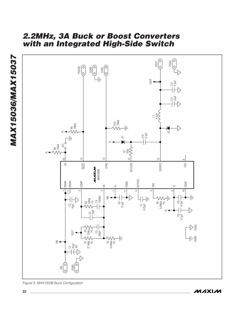
Figure 5. MAX15036 Buck Configuration

MA
X1
50
36
/MA
X1
50
37
2.2MHz, 3A Buck or Boost Converterswith an Integrated High-Side Switch
______________________________________________________________________________________ 23
MAX
1503
7
12
56
4
N1 3
R6 4.7Ω
91215
R7 15Ω
D1
VL
131416
R8 10kΩ JU
1VL
VL
R9 10kΩ
PGOO
D
SGND
SYNC
R10
10kΩ
C10
0.1μ
F
108
C94.
7μF
C80.
1μF
VL
R56.
04kΩ 1%
SGND
PGND
C70.
22μF
C60.
1μF
VIN
7 11 6 54
C3 1200
pF
R4 10kΩ
1%C4 22
pF
R375
0Ω 1% C533
0pF
R127
.4kΩ 1% R2
6.04
kΩ 1%
VIN
PGND
+C1 47
μF35
VVIN
VOUT
C210
μF
1 2 3
EN
PGOO
D
SYNC
BST/
VDD
SOUR
CE DLSG
ND
V LOSC
BYPA
SS
PGND
V+FBCOM
P
DRAI
N
DRAI
N
D2
L14.
7μH C1
122
μF
VOUT
VOUT
PGND
C12
0.1μ
F
Figure 6. MAX15037 Buck Configuration

MA
X1
50
36
/MA
X1
50
37
2.2MHz, 3A Buck or Boost Converterswith an Integrated High-Side Switch
24 ______________________________________________________________________________________
Figure 7. MAX15036 Boost Configuration
MAX15036
JU1
VL
PGOOD
SGND
VIN
VOUT
PGND
SYNC
VIN
VL
VL
R127.4kΩ
1%
R26.04kΩ
1%
R422.1kΩ
1%
R810kΩ
R56.04kΩ1%
R1010kΩ
R910kΩ
1DRAIN
2DRAIN
3COMP
7V+
6BYPASS
4FB
16EN
15BST/VDD
12SOURCE
9CKO
5OSC
13SYNC
14RESET
C100.1μF
VIN
11PGND
C60.1μF
VL
C80.1μF
8VL
10SGND
C94.7μF
SGND PGND
D2
L14.7μH
C210μF
C32200pF
R31kΩ1%C5
560pF
C1122μF
C120.1μF
C147μF
35V
VOUT
VOUT
PGND
C422pF
C70.22μF

MA
X1
50
36
/MA
X1
50
37
2.2MHz, 3A Buck or Boost Converterswith an Integrated High-Side Switch
Maxim cannot assume responsibility for use of any circuitry other than circuitry entirely embodied in a Maxim product. No circuit patent licenses areimplied. Maxim reserves the right to change the circuitry and specifications without notice at any time.
Maxim Integrated Products, 120 San Gabriel Drive, Sunnyvale, CA 94086 408-737-7600 ____________________ 25
© 2008 Maxim Integrated Products is a registered trademark of Maxim Integrated Products, Inc.
V+DRAIN
OUTPUT1
CIN
VIN
SOURCE
CLKOUT
MASTER
SYNC
SYNC
CLKOUT(MASTER)
SOURCE(MASTER)
SOURCE(SLAVE)
CLKIN
DUTY CYCLE = 50%
V+DRAIN
SOURCE
SLAVE
SYNC
OUTPUT2
SYNCPHASE
CLKOUTPHASE
Figure 8. Synchronized Converters
15
16
14
13
6
5
7
DRAI
N FB
8
DRAI
N
PGND
DLSOUR
CE
1
+
2
PGOOD
4
12 11 9
BST/VDD
EN
VL
V+
BYPASS
OSC
MAX15037
COM
PSG
ND
3
10
SYNC
THIN QFN5mm x 5mm
TOP VIEW
EP*
*EXPOSED PAD.
Pin Configurations (continued) Chip InformationPROCESS: BiCMOS
Package InformationFor the latest package outline information and land patterns, goto www.maxim-ic.com/packages.
PACKAGE TYPE PACKAGE CODE DOCUMENT NO.
16 TQFN T1655-2 21-0140