zynq phd pedre tesis
DESCRIPTION
Tesis Doctoral SoC - FPGATRANSCRIPT

Universidad de Buenos AiresFacultad de Ciencias Exactas y Naturales
Departamento de Computacion
Una nueva metodologıa paraco-diseno de sistemas embebidos
centrados en procesadorusando FPGAs
Tesis presentada para obtener el tıtulo de Doctorde la Universidad de Buenos Aires
en el area Ciencias de la Computacion
Sol Pedre
Directora: Dra. Patricia Borensztejn
Director Asistente: Dr. Elıas Todorovich
Lugar de Trabajo: Departamento de Computacion, Facultad de CienciasExactas y Narurales, Universidad de Buenos Aires.
Buenos Aires, 2013

Una nueva metodologıa para co-diseno de
sistemas embebidos centrados en procesador
usando FPGAs
Hoy en dıa, los sistemas embebidos son partes vitales de equipos de co-municaciones, sistemas de transporte, plantas de energıa, electronica de con-sumo, robotica entre muchos otros. Su amplio campo de aplicacion y lascrecientes complejidades de sus disenos torna esencial la propuesta de nuevasmetodologıas, lenguajes y herramientas. El objetivo de esta tesis doctoral escontribuir al campo del co-diseno hardware/software de sistemas embebidos.
Primero, presentamos el co-diseno de un sistema embebido de control apli-cando el flujo de diseno tradicional, que combina procesadores y circuitos in-tegrados (ICs): el desarrollo de un nuevo mini-robot llamado ExaBot. Luego,introducimos un flujo de diseno tradicional para Field Programmable Gate Ar-rays (FPGA), y lo aplicamos a un problema de sensado remoto: procesar videoinfrarrojo en tiempo real en un UAV (Unmanned Aerial Vehicle). Finalmente,de la observacion de las dificultades en experiencias anteriores, y analizandolas tendencias y tecnologıas actuales, proponemos una nueva metodologıa deco-diseno para sistemas embebidos centrados en procesador usando FPGAs.Este es un creciente y novedoso campo de los sistemas embebidos: durante2011, tanto Xilinx como Altera (los dos fabricantes mas grandes de FPGAs)lanzaron nuevas familias de chips que combinan potentes procesadores ARMcon logica programable de bajo consumo.
El objetivo de la nueva metodologıa de co-diseno es lograr soluciones embe-bidas de tiempo real, utilizando aceleracion por hardware, pero con un tiempode desarrollo similar al de proyectos de software. Para ello, combinamosmetodologıas y herramientas bien establecidas del mundo del software, comoDiseno Orientado a Objetos, UML, y programacion multi-hilos, con nuevas tec-nologıas del mundo del hardware, como herramientas semi-automaticas parasıntesis de alto nivel. La metodologıa propuesta fue aplicada a un algoritmode localizacion de multiples robots en un sistema de vision global. La solucionembebida final procesa 32 imagenes de 1600 × 1200 pıxeles por segundo, lo-grando una aceleracion de 16× con respecto a la solucion de software masoptimizada, con un 43% de incremento en area pero un 92% de ahorro deenergıa.
i

A new co-design methodology for
processor-centric embedded systems in
FPGA-based chips
Embedded systems are nowadays vital parts of communication equipment,transportation systems, power plants, consumer electronics, robotics amongmany others. Their vast field of application and the growing complexitiesof their designs turn the proposal of new methodologies, languages and toolsessential. The goal of this thesis is to make such contributions in the field ofhardware/software co-design of embedded systems.
First, we present the co-design of a control embedded system applying thetraditional flow in which processors and off-the-shelf Integrated Circuits (ICs)are combined: the development of a mini-robot called ExaBot. Secondly, weintroduce a traditional Field Programmable Gate Array design flow, and ap-ply it to a remote sensing application that processes real-time video from aninfrared camera on an UAV (Unmanned Aerial Vehicle). Finally, from theobservation of difficulties in previous experiences and analyzing current tech-nologies and trends, we propose a new co-design methodology for processor-centric embedded systems in FPGA-based chips. This is a growing and novelfield of embedded systems: during 2011, both Xilinx and Altera (the two lead-ing FPGA vendors) launched new chip families that combine powerful ARMprocessor cores with low-power programmable logic.
The goal of the proposed co-design methodology is to achieve real-timeembedded solutions, using hardware acceleration, but with development timesimilar to that of software projects. For this, well-established methodologiesand tools from the software domain, such as Object Oriented Design, UnifiedModeling Language or multithreaded programming, are combined with newtechniques from the hardware world, like semi-automatic high level synthesistools. The proposed methodology was successfully applied to a multiple robotlocalization algorithm in a global vision system. The final embedded solutionprocesses 1600× 1200 pixel images at 32 frames per second, achieving a 16×acceleration with respect to the most optimized software solution, with a 43%increase in area but a 92% energy saving.
ii

Contents
1 Introduction 2
1.1 Motivation . . . . . . . . . . . . . . . . . . . . . . . . . . . . . 2
1.2 Research goal . . . . . . . . . . . . . . . . . . . . . . . . . . . 4
1.3 Outline of the thesis . . . . . . . . . . . . . . . . . . . . . . . 4
2 Embedded systems using processors and ICs: ExaBot, a newmobile mini-robot 6
2.1 Introduction . . . . . . . . . . . . . . . . . . . . . . . . . . . . 7
2.2 Co-Design Flow . . . . . . . . . . . . . . . . . . . . . . . . . . 10
2.2.1 Goals Specification. Body, locomotion and sensors defi-nition . . . . . . . . . . . . . . . . . . . . . . . . . . . 11
2.2.2 Partition in subsystems . . . . . . . . . . . . . . . . . . 12
2.2.3 Design Refinement & Testing of each subsystem . . . . 12
2.2.4 Subsystems integration & Testing . . . . . . . . . . . . 13
2.2.5 Final mounting . . . . . . . . . . . . . . . . . . . . . . 14
2.3 Case Study: ExaBot development . . . . . . . . . . . . . . . . 14
2.3.1 Goal Definition . . . . . . . . . . . . . . . . . . . . . . 14
2.3.2 Body, sensors and locomotion definition . . . . . . . . 14
2.3.3 Partition in Subsystems . . . . . . . . . . . . . . . . . 20
2.3.4 Subsystem Refinement: Motor Control . . . . . . . . . 23
2.3.5 Subsystem Refinement: Sensor Control . . . . . . . . . 30
2.3.6 Subsystem Integration . . . . . . . . . . . . . . . . . . 36
2.3.7 Subsystem Integration: Communication . . . . . . . . 37
iii

2.3.8 Subsystem Integration: Programming . . . . . . . . . . 43
2.3.9 Subsystem Integration: Power . . . . . . . . . . . . . . 44
2.3.10 Subsystem Integration: Design and Test of the final PCB 45
2.3.11 Final Mounting . . . . . . . . . . . . . . . . . . . . . . 47
2.4 Applications . . . . . . . . . . . . . . . . . . . . . . . . . . . . 47
2.4.1 Research: Autonomous visual navigation . . . . . . . . 48
2.4.2 Outreach . . . . . . . . . . . . . . . . . . . . . . . . . . 49
2.4.3 Undergraduate Education . . . . . . . . . . . . . . . . 50
2.5 Publications . . . . . . . . . . . . . . . . . . . . . . . . . . . . 50
2.6 Conclusions . . . . . . . . . . . . . . . . . . . . . . . . . . . . 52
3 Embedded Systems using FPGAs: Real-time hotspot detec-tion 53
3.1 Introduction . . . . . . . . . . . . . . . . . . . . . . . . . . . . 54
3.1.1 What is an FPGA? . . . . . . . . . . . . . . . . . . . . 54
3.1.2 Why are FPGAs of interest? . . . . . . . . . . . . . . . 55
3.1.3 What are FPGAs used for? . . . . . . . . . . . . . . . 55
3.2 FPGA Basic Architecture . . . . . . . . . . . . . . . . . . . . 57
3.2.1 Logic Blocks . . . . . . . . . . . . . . . . . . . . . . . . 57
3.2.2 Routing Matrix & Global Signals . . . . . . . . . . . . 58
3.2.3 I/O Blocks . . . . . . . . . . . . . . . . . . . . . . . . . 59
3.2.4 Clock Resources . . . . . . . . . . . . . . . . . . . . . . 60
3.2.5 Embedded Memory . . . . . . . . . . . . . . . . . . . . 60
3.2.6 Multipliers, Adders, DPS blocks . . . . . . . . . . . . . 61
3.2.7 Advanced features . . . . . . . . . . . . . . . . . . . . 62
3.2.8 The complete picture . . . . . . . . . . . . . . . . . . . 63
3.3 Design Flows for FPGA . . . . . . . . . . . . . . . . . . . . . 63
3.3.1 Architecture Phase . . . . . . . . . . . . . . . . . . . . 64
3.3.2 Implementation Phase . . . . . . . . . . . . . . . . . . 65
3.3.3 FPGA flows comparison . . . . . . . . . . . . . . . . . 76
iv

3.4 Case Study: Real time hot spot detection using FPGA . . . . 79
3.4.1 Requirements and Specification . . . . . . . . . . . . . 80
3.4.2 Architecture . . . . . . . . . . . . . . . . . . . . . . . . 82
3.4.3 Implementation . . . . . . . . . . . . . . . . . . . . . . 89
3.4.4 Solution sizing . . . . . . . . . . . . . . . . . . . . . . . 95
3.4.5 Experiments and Results . . . . . . . . . . . . . . . . . 96
3.5 Conclusions . . . . . . . . . . . . . . . . . . . . . . . . . . . . 101
4 A new co-design methodology for processor-centric embeddedsystems in FPGAs: Vision-based multiple robot localization 103
4.1 Related Work . . . . . . . . . . . . . . . . . . . . . . . . . . . 105
4.1.1 Vision-based multiple robot localization . . . . . . . . 105
4.1.2 Co-designed FPGA solutions for image processing algo-rithms related to robotic localization . . . . . . . . . . 106
4.1.3 High level modeling and high level synthesis . . . . . . 108
4.2 Methodology . . . . . . . . . . . . . . . . . . . . . . . . . . . 110
4.2.1 OOP Design . . . . . . . . . . . . . . . . . . . . . . . . 110
4.2.2 C++ Implementation and Testing . . . . . . . . . . . . 112
4.2.3 Software Migration, optimization and HW/SW partition 113
4.2.4 Hardware translation, testing and integration . . . . . 116
4.3 Multiple Robot Localization . . . . . . . . . . . . . . . . . . . 121
4.3.1 Method overview . . . . . . . . . . . . . . . . . . . . . 121
4.3.2 Image rectification . . . . . . . . . . . . . . . . . . . . 122
4.3.3 Position estimation . . . . . . . . . . . . . . . . . . . . 123
4.3.4 Orientation calculation . . . . . . . . . . . . . . . . . . 123
4.3.5 Robot identification . . . . . . . . . . . . . . . . . . . . 124
4.4 Hardware/Software co-designed solution . . . . . . . . . . . . 124
4.4.1 OOP Design . . . . . . . . . . . . . . . . . . . . . . . . 125
4.4.2 C++ Implementation and Testing . . . . . . . . . . . . 127
4.4.3 Software Migration, optimization and HW/SW partition 128
v

4.4.4 Hardware translation, testing and integration . . . . . 131
4.5 Acceleration, area and power consumption results and analysis 137
4.5.1 Acceleration . . . . . . . . . . . . . . . . . . . . . . . . 137
4.5.2 Area . . . . . . . . . . . . . . . . . . . . . . . . . . . . 142
4.5.3 Power and Energy consumption . . . . . . . . . . . . . 142
4.5.4 Overall analysis . . . . . . . . . . . . . . . . . . . . . . 144
4.6 Conclusions . . . . . . . . . . . . . . . . . . . . . . . . . . . . 146
5 Conclusions 147
5.1 Embedded systems using processors and ICs . . . . . . . . . . 148
5.2 Embedded systems using FPGAs . . . . . . . . . . . . . . . . 148
5.3 A new co-design methodology for processor-centric embeddedsystems in FPGA-based chips . . . . . . . . . . . . . . . . . . 149
5.4 Publications . . . . . . . . . . . . . . . . . . . . . . . . . . . . 151
5.5 Future work . . . . . . . . . . . . . . . . . . . . . . . . . . . . 153
Appendices 154
Appendix A Exabot Schematics and PCB 155
vi

List of Figures
2.1 Robots for hostile environments. Space exploring rovers: a) Thesoviet Lunokhod, b) NASA’s Spirit, Sojouner and Curiosity.On Earth: c) Airduct inspection robot d) iRobot’s 510 PackBotused at Fukushima Daiichi Nuclear Power Station in Japan e)KonaBot Robot for bomb control constructed at our lab . . . 8
2.2 Service Robots: a) Roomba 790 vacuum cleaning b) KA Lawn-Bott LB1200 Spyder Lawnmower c) Genibo pet robot . . . . 8
2.3 Research Robots: a) Adept’s Pioneer 3-DX robot b)K-TeamKhepera II mini robot . . . . . . . . . . . . . . . . . . . . . . 9
2.4 Co-design flow for the ExaBot. The horizontal swimlines showthe equivalent stages from traditional general co-design flow. . 11
2.5 The Traxster mechanical kit . . . . . . . . . . . . . . . . . . . 16
2.6 Pulse Width Modulation . . . . . . . . . . . . . . . . . . . . . 24
2.7 Motor subsystem diagram . . . . . . . . . . . . . . . . . . . . 25
2.8 Proportional Integrative Derivative Control . . . . . . . . . . . 26
2.9 Sequence diagram showing the interaction of the different mod-ules to achieve the PID control . . . . . . . . . . . . . . . . . 27
2.10 Prototyping boards: a) Breadboard, b) Stripboard, c) Perf-board . . . . . . . . . . . . . . . . . . . . . . . . . . . . . . . 29
2.11 Prototype board for the Motor control with Faulhaber motorconnected. It includes a PIC18F2431, a L293 driver in the upperleft and a LM7805 in the bottom left. The other IC is a MAX232for USART. . . . . . . . . . . . . . . . . . . . . . . . . . . . . 30
2.12 Infrared range finder timing diagram. . . . . . . . . . . . . . . 31
2.13 Infrared range finder analog output voltage vs distance to re-flective object. . . . . . . . . . . . . . . . . . . . . . . . . . . . 31
2.14 Sonar Timing Diagram . . . . . . . . . . . . . . . . . . . . . . 32
vii

2.15 Sensor subsystem diagram . . . . . . . . . . . . . . . . . . . . 33
2.16 Sequence diagram showing the interaction of the different mod-ules to achieve Sonar control . . . . . . . . . . . . . . . . . . . 35
2.17 Prototype board for the Sensor control with a GP2D120 rangefinder connected. The cables for SPI communication can beseen in the right, the ones for Vcc and Gnd in the left. . . . . 36
2.18 Typical configuration of SPI bus for one master and three slaves 37
2.19 Sequence diagram showing the interactions between the differ-ent OSI layers to implement the network protocol dispatchingroutine. . . . . . . . . . . . . . . . . . . . . . . . . . . . . . . 41
2.20 State Diagram showing a typical interaction of Phisycal, Linkand Application layers to send and receive a packet . . . . . . 42
2.21 Prototype boards for communication subsystem. In this config-uration, the prototype board of the Motor Control is connectedto the PC104 through the perfboard with the CD4050B IC. . . 43
2.22 Four different configurations of the ExaBot: a) with all the sen-sors and PC104 b) with a smart phone, c) with a netbook anda 3D Minoru Camera, d) with an embedded Mini-ITX boardand a FireWire Camera . . . . . . . . . . . . . . . . . . . . . 47
2.23 Easy Robot Behavior-Based Programming Interface: a) Mainview. The upper panel shows the main control functions: left:new, open, save. center: play, new timer, new counter.right:close, b) A screen shot of the Braitenberg view. The left panelshows the robot schema and the transfer functions that canbe used (top-down: inhibitory, excitatory, broken, constant).In the center of the work canvas all the sensors are shown(top-down: 2 line-followings, 6 infrared telemeters, 1 sonar, 2bumpers). The wheels are shown on each side of the work can-vas. The programmed behavior is a simple explorer that movesaround at constant speed and can avoid obstacles . . . . . . . 49
3.1 FPGA market by end application . . . . . . . . . . . . . . . . 56
3.2 Simplified Xilinx Logic Cell (figure taken from [1]) . . . . . . . 58
3.3 Simplified Xilinx CLB, comprising 4 Slices of 2 Logic Cells each.(figure taken from [1]) . . . . . . . . . . . . . . . . . . . . . . 58
3.4 FPGA routing signal (figure taken from [2]) . . . . . . . . . . 59
3.5 I/O block . . . . . . . . . . . . . . . . . . . . . . . . . . . . . 59
viii
3.6 A simple clock tree (figure taken from [1]). . . . . . . . . . . . 60
3.7 Clock Manager (figure taken from [1]). . . . . . . . . . . . . . 61
3.8 Embedded memory block. . . . . . . . . . . . . . . . . . . . . 61
3.9 Digital Signal Processing blocks . . . . . . . . . . . . . . . . . 62
3.10 Generic FPGA architecture (figure taken from [2]) . . . . . . . 63
3.11 Activity diagram of the Implementation phase of FPGA designflow . . . . . . . . . . . . . . . . . . . . . . . . . . . . . . . . 66
3.12 VHDL and Verilog levels of abstraction . . . . . . . . . . . . . 67
3.13 Block diagram of a synchronous system (figure taken from [3]) 69
3.14 Block Diagram of a Data Path - Controller Architecture (figuretaken from [3]) . . . . . . . . . . . . . . . . . . . . . . . . . . 72
3.15 Block diagram of full testbench- DUT stands for Design UnderTest (figure taken from [4]). . . . . . . . . . . . . . . . . . . . 75
3.16 Design flow presented in Chu’s book [3] (see page 16 of the book) 77
3.17 Design flow presented in Maxfield’s book [1] (see page 159 ofthe book) . . . . . . . . . . . . . . . . . . . . . . . . . . . . . 77
3.18 Design flow presented in Kilts’s book [5] (see page 9 of the book) 78
3.19 Design flow for the Implementation stage in Cofer’s book [2](see page 121 of the book) . . . . . . . . . . . . . . . . . . . . 79
3.20 Design flow in Wolf’s book [6] (see page 414 of the book) . . . 80
3.21 Line of previous pixels stored in L. . . . . . . . . . . . . . . . 82
3.22 Hardware platform including the video digitalizer, the FPGAand Ethernet physical driver. . . . . . . . . . . . . . . . . . . 82
3.23 First view of the hierarchichal design . . . . . . . . . . . . . . 84
3.24 Camera control module architecture . . . . . . . . . . . . . . . 85
3.25 Initial Architecture for the Image Segmentation module. Theclock is the 27 Mhz digitalizer clock. Both the clock and resetsignals are distributed to all the submodules, although this isnot shown in the figure for simplicity. . . . . . . . . . . . . . . 88
3.26 Final Architecture for the Image Segmentation module. . . . . 89
3.27 Architecture of the Net Control module. . . . . . . . . . . . . 90
3.28 Line L of previous pixels implemented as a stack. . . . . . . . 91
ix

3.29 Detailed implementation of the stack L in the Raw Processingmodule, including the general middle records and the specialtop and bottom records of the stack. . . . . . . . . . . . . . . 92
3.30 HotSpot Reconstructor module. . . . . . . . . . . . . . . . . . 93
3.31 Detail of the logic for the maximum calculation in the hotSpotReconstructor Module . . . . . . . . . . . . . . . . . . . . . . 93
3.32 a hotspot image after classification in hot or cold pixels. bvisual representation of the results showing the location of thedetected hotspot (the centroid is not shown). . . . . . . . . . . 97
4.1 Lighting conditions on the SyRoTek Arena. . . . . . . . . . . . 107
4.2 Methodology overview . . . . . . . . . . . . . . . . . . . . . . 111
4.3 Activity Diagram for the software migration, optimization andHW/SW partition stage . . . . . . . . . . . . . . . . . . . . . 114
4.4 Activity Diagram for the hardware translation, testing and in-tegration stage, including the choices to use the AutoESL toolor the hand-coded two-process . . . . . . . . . . . . . . . . . . 117
4.5 SyRoTek arena and robot with dress arc. . . . . . . . . . . . . 121
4.6 Original and rectified arena image. . . . . . . . . . . . . . . . 122
4.7 Rectified image part and convolution filter response . . . . . . 123
4.8 Orientation and identification process . . . . . . . . . . . . . . 124
4.9 Structural Design . . . . . . . . . . . . . . . . . . . . . . . . . 125
4.10 Sequence Diagram for the calculation of the new position of onerobot . . . . . . . . . . . . . . . . . . . . . . . . . . . . . . . . 126
4.11 Activity Diagram showing the parallel nature of the new posi-tion and orientation calculation for each robot (two robots inthis diagram). . . . . . . . . . . . . . . . . . . . . . . . . . . 127
4.12 Profiling results for software optimizations in the PPC. . . . . 131
4.13 Profiling results for hardware acceleration . . . . . . . . . . . 134
4.14 Execution times of all solutions . . . . . . . . . . . . . . . . . 138
4.15 Acceleration of each hardware accelerated solution comparedwith software solutions . . . . . . . . . . . . . . . . . . . . . . 139
4.16 Acceleration achieved with respect to Amdahl’s theoretical max-imum . . . . . . . . . . . . . . . . . . . . . . . . . . . . . . . . 140
x

4.17 Acceleration of each additional hardware ipcore, as comparedwith the solution with only one hardware ipcore. . . . . . . . . 141
4.18 Percentage of extra slices occupied as compared with the onlysoftware solution . . . . . . . . . . . . . . . . . . . . . . . . . 143
4.19 Estimated energy consumption per frame for each solution . . 144
4.20 Estimated energy saving . . . . . . . . . . . . . . . . . . . . . 145
xi

List of Tables
2.1 Classification of the most useful sensors for mobile robot appli-cations (table taken from [7]) . . . . . . . . . . . . . . . . . . 17
2.2 Characteristics of the ExaBot sensors. NA: Not Applicable, NI:Not Informed, Rs: Resistance . . . . . . . . . . . . . . . . . . 20
2.3 Network layer packet formats. This can be extended if newsensors are added. sensor: 0x00 : three left range finders,0x01: three middle range finders, 0x02, three right range find-ers, 0x03:sonar, 0x04: line-following, 0x05: bumper . . . . . . 40
2.4 Typical and Maximum consumption rates of the main(i.e., mostconsuming) ICs and sensors to estimate the 5V battery require-ments. All measures in mA. PICs running at 40 Mhz. . . . . . 45
3.1 Raw processing output signals according to the situation. . . . 86
3.2 Code sizing . . . . . . . . . . . . . . . . . . . . . . . . . . . . 97
3.3 Area occupied by the complete solution . . . . . . . . . . . . 98
3.4 Advanced HDL Synthesis Report Macro Statistics for Raw Pro-cessing module . . . . . . . . . . . . . . . . . . . . . . . . . . 99
4.1 Profiling results for software optimizations. Times for completesolution in milliseconds. . . . . . . . . . . . . . . . . . . . . . 130
4.2 Profiling results for hardware accelerated solution. . . . . . . . 133
4.3 Profiling results with one, two, four and six hardware accelerators134
4.4 ROCCC and Two-Process comparison for vector MACC . . . 136
4.5 AutoESL and Two-Process comparison for Matrix::macc . . . 136
4.6 Area occupied by each solution. Hardware implemented usingtwo-process. . . . . . . . . . . . . . . . . . . . . . . . . . . . . 142
xii

4.7 Power and Energy consumption. Hardware implemented usingtwo-process. . . . . . . . . . . . . . . . . . . . . . . . . . . . . 144
1

Chapter 1
Introduction
1.1 Motivation
An embedded system is a system designed to perform one or few dedicatedfunctions and that is embedded into a larger device [8, 9]. Common char-acteristics include efficiency in terms of energy, cost and weight; reliabilitysince they are often components of critical systems; and the need to meet real-time constraints. Nowadays, embedded systems are vital parts of communica-tion equipment, transportation systems, power plants, consumer electronics,robotics among many others [10].
Most embedded systems include off-the-shelve ICs (Integrated Circuits) forspecific functions together with one or many processor elements, i.e., micro-controllers, microprocessors or DSPs (Digital Signal Processors). The designof systems that have software running in processors interacting with hardwaremodules is called hardware/software co-design. Already in 2004, over 90 % ofembedded systems included some kind of processor [11], and from the 9 billionprocessors manufactured in 2005, 98% was used in embedded systems [12].According to the 2012 Embedded Market Survey conducted by EEtimes andEmbedded magazines [13], 97% of the 1,700 consulted embedded engineerswere using at least one processor in their designs. This makes research in co-design methodologies and tools a key field in the embedded system domain.
However, some systems require massive data processing with real-time con-straints that cannot be met with this standard approach. Examples includedigital signal processing methods such as image, video or audio processing, andtheir applications to robotics, remote sensing, consumer electronics amongmany other fields. In these cases, solutions include the use of Field Pro-grammable Gate Arrays (FPGAs) or the design and implementation of ASICs(Application Specific Integrated Circuits). These approaches take advantage ofthe inherent parallelism of many data processing algorithms and allow to cre-
2

ate massive parallel solutions. They also allow tailored hardware acceleration,e.g., with particular memory access patterns or bit tailored multipliers/adders.ASICs provide the best solution in terms of performance, unit cost and powerconsumption. FPGAs are designed to be configured by a designer after manu-facturing— hence “field-programmable”. The ability to update the function-ality after shipping, partial re-configuration of a portion of the design, and thelower non-recurring engineering costs and shorter time-to-market comparedto an ASIC design, offer advantages for many applications. According to the2012 Embedded Market Survey, 35% of the surveyed engineers are currentlyusing FPGAs in their designs [13].
For many applications designing the entire system in FPGAs or hardwareis not the most practical solution. Even the most data intensive processingmethods frequently contain sequential sections that are easier implemented inprocessors. These hardware/software co-designed solutions try to combine thebest of both software and hardware worlds, making use of the ease of program-ming a processor while designing tailored hardware accelerator modules for themost time-consuming sections of the application. This not only accelerates theresulting system compared to the processor solution, but also allows savings inenergy. The inclusion of processor cores embedded in programmable logic hasmade FPGAs an excellent platform for these approaches. During 2011, thetwo major FPGA vendors (Xilinx and Altera) announced new chip familiesthat combine powerful ARM processor cores with low-power programmablelogic [14, 15]. While FPGA vendors have previously produced devices withon-board processors, the new families are unique in that the ARM processorsystem, rather than the programmable logic, is the center of the chip [16].This strengthens the growing trend towards co-designed processor-centric so-lutions in FPGA-based chips [17]. According to the 2012 Embedded MarketSurvey, 37 % of the engineers that do not use FPGAs in their current designsconfirmed that this trend will change their minds [13].
The novelty of this approach together with its potential in the embed-ded system world makes academic research in hardware/software co-design inFPGA-based chips an important field. The main problem to tackle is time-consuming development. The rising complexity of these applications makeit difficult for designers to model the functional intent of the system in lan-guages that are used for implementation such as C or HDLs (Hardware De-scription Languages). Moreover, the difficulty of programming FPGAs in HDLis pointed out by engineers as an important reason for not using FPGAs [13].This poses a strong need for methodologies, languages and tools that reducedevelopment time and complexity by raising the abstraction level of designand implementation [18] [19]. Advances have been made in high-level mod-eling using specific Unified Modeling Language (UML) profiles to simplifydesign. Also, much work is being done in high-level synthesis tools, whichtranslate constructs in C/C++ to HDL to simplify hardware implementation.
3

However, there is still much research needed in co-design methodologies, lan-guages and tools so that the recent combination of powerful processors withprogrammable logic can raise to its full potential.
1.2 Research goal
The goal of this thesis is to make a contribution in the field of hardware/softwareco-design of embedded systems. We expect that the developed work will helpreduce design and implementation effort in an important field of embedded sys-tems design, at a time when the growing complexities of these designs makethe need for new methodologies, languages and tools vital.
The particular research goals in this thesis are:
1. the study of traditional co-design flows using processors and off-the-shelfICs, and their application to the co-design of an embedded system withreal-time, power consumption and size requirements.
2. the study of traditional design flows using FPGAs and their applicationto the design of an embedded system that require massive data processingwith real-time constraints
3. the proposal of a new co-design methodology for a significant class ofembedded systems: processor-centric embedded systems with hardwareacceleration in FPGA-based chips. The new methodology will be focusedin reducing design and implementation effort, integrating methodologies,languages and tools from both the software and hardware domain.
1.3 Outline of the thesis
In this thesis we present designs in each of the mentioned fields of embeddedsystems and we propose a new co-design methodology for processor-centricembedded systems with hardware acceleration in FPGA-based chips.
Chapter 2 is devoted to the co-design of a control embedded system apply-ing the traditional flow in which processors and off-the-shelf ICs are combined:the development of a mini-robot called ExaBot [20]. This system has stringentreal-time, power consumption and size requirements, providing a case studyfor traditional co-design flows. The main goal for pursuing this task was toobtain a low-cost robot that could be used not only for research, but alsofor outreach activities and education. In this sense, neither the commerciallyavailable research robots nor the commercially available educational robotswere considered a suitable solution. Six ExaBot robots are currently in use
4

in the Laboratorio de Robotica y Sistemas Embebidos of the FCEN-UBA.They have been used for educational robotics activities for high school stu-dents, research experiments in mobile robotics, and education in graduate andundergraduate university courses.
In chapter 3 we introduce a traditional FPGA design flow and apply it toa remote sensing application [21]. The application processes real-time videofrom an infrared camera on an UAV (Unmanned Aerial Vehicle) in order tofind the location and spatial configuration of the hot spots present in eachframe. The proposed method successfully segments the image with a totalprocessing delay equal to the acquisition time of one pixel (that is, at videorate). The processing delay is independent of the image size. This real-timemassive data processing was possible because the algorithm was designed forparallel FPGA implementation, and it was fully implemented in programmablelogic and hardware ICs.
In chapter 4 we propose a new co-design methodology for processor-centricembedded systems with hardware acceleration in FPGA-based chips [22, 23,24]. The aim of the methodology is to achieve real-time embedded solu-tions using hardware acceleration, but with development times similar to soft-ware projects. To reduce the development time, well established methodolo-gies, techniques and languages from the software domain are applied, suchas Object-Oriented Paradigm design, Unified Modeling Language and mul-tithreaded programming. Moreover, to reduce hardware coding effort, semi-automatic C-to-HDL translation tools and methods are used and compared.As a case study, we use a robust algorithm for multiple robot localization inglobal vision systems. This algorithm integrates an e-learning robotic labo-ratory for distance education that allows students from all over the world toperform experiments with real robots in an enclosed arena. The co-designedimplementation of this algorithm following the proposed methodology showsthe usefulness of the methodology for embedded real-time massive data pro-cessing applications.
In chapter 5 conclusions and future work are outlined.
5

Chapter 2
Embedded systems usingprocessors and ICs
ExaBot, a new mobile mini-robot
Most embedded systems include off-the-shelve ICs (Integrated Circuits) forspecific functions together with one or many processor elements, i.e. micro-controllers, microprocessors or DSPs (Digital Signal Processors). The designof systems that have software running in processors interacting with hardwaremodules is called hardware/software co-design. Already in 2004, over 90 % ofembedded systems included some kind of processor [11], and from the 9 billionprocessors manufactured in 2005, 98% were used in embedded systems [12].According to the 2012 Embedded Market Survey conducted by EEtimes andEmbedded magazines [13], 97% of the 1,700 consulted embedded engineerswere using at least one processor in their designs. This makes research in co-design methodologies and tools a key field in the embedded system domain.
This chapter is devoted to the co-design of a control embedded systemapplying the traditional flow in which processors and off-the-shelve ICs arecombined: the development of a mini-robot called ExaBot [20]. This systemhas stringent real-time, power consumption and size requirements, providing achallenging case study for traditional co-design flows. The main contributionsin this chapter are:
• The adaptation of traditional co-design flows in which processors andoff-the-shelve ICs are combined to the autonomous robotics field. Theparticular co-design flow is explained and the development of the robotfollowing its different stages is shown.
• The design, construction and testing of the ExaBot robots. The maingoal for pursuing this task was to obtain a low-cost robot that could beused not only for research, but also for outreach activities and educa-
6

tion. In this sense, neither the commercially available research robotsnor the commercially available educational robots were considered a suit-able solution. Six ExaBot robots are currently in use in the Laboratoriode Robotica y Sistemas Embebidos of the FCEN-UBA. They have beenused for educational robotics activities for high school students, researchexperiments in mobile robotics, and education in graduate and under-graduate university courses.
This chapter is organized as follows: section 2.1 offers a short introductionto mobile robotics and the reasons for choosing this case study. Section 2.2presents the co-design and testing methodology followed. The developmentof each stage to construct the ExaBot is presented in section 2.3. Section 2.4comments several successful research, education and outreach activities carriedout with the ExaBot. Finally, section 2.6 shares some conclusions.
2.1 Introduction
Robotics has achieved its greatest success to date in the world of industrialmanufacturing1. Robot arms, or manipulators, comprised a US$ 5,7 billionmarket in 2010, totaling 1,035,000 units installed in factories around the world[25]. Yet, for all of their successes, these commercial robots suffer from afundamental disadvantage: lack of mobility. A fixed manipulator has a limitedrange of motion, that depends on where it is bolted down. In contrast, a mobilerobot would be able to travel throughout the manufacturing plant, flexiblyapplying its talents wherever it is most effective [26].
Mobile robots can be found in many fields. One of the most importantapplications is their use in hostile or inhospitable environments for humanbeings. For example, using mobile robots is nowadays the only viable optionof exploring other planets. From the Soviet Lunokhod 12 that landed on theMoon in November 17, 1970 to the recent Curiosity that landed on Mars, a longline of mobile robots have been developed to handle the extreme conditionsof outer space. In dangerous and inhospitable environments on Earth, suchteleoperated systems have also gained popularity (see Fig. 2.1).
Other commercial robots operate not where humans cannot go but rathershare space with humans in human environments. In 2010, about 2.2 millionservice robots for personal and domestic use were sold, for a value of US$ 538million [27]. So far, service robots for personal and domestic use are mainlyin the areas of domestic robots, which include vacuum cleaning, lawn-mowing,
1Industrial robots are defined by ISO 8373 as “An automatically controlled, repro-grammable, multipurpose manipulator programmable in three or more axes which maybe either fixed in place or mobile for use in industrial automation applications.”
2The first mobile robot which landed on any celestial body
7

(a) Lunokhod (b) NASA Rovers
(c) Air-duct Robot (d) M510 (e) KonaBot
Figure 2.1: Robots for hostile environments. Space exploring rovers: a) The sovietLunokhod, b) NASA’s Spirit, Sojouner and Curiosity. On Earth: c) Airduct in-spection robot d) iRobot’s 510 PackBot used at Fukushima Daiichi Nuclear PowerStation in Japan e) KonaBot Robot for bomb control constructed at our lab
pool cleaning, toy robots and hobby systems. Educational robots are also agrowing field, being the Lego Mindstrom the most popular kits for educationalrobotics activities [28]. For a good idea of the amount, price and availabilityof service robots see [29].
(a) Roomba (b) LawnBott (c) Genibo
Figure 2.2: Service Robots: a) Roomba 790 vacuum cleaning b) KA LawnBottLB1200 Spyder Lawnmower c) Genibo pet robot
Although mobile robots can be found in many fields as already discussed,achieving a fully autonomous robot is still a major task in robotics. The fun-damental question is: how can a mobile robot move unsupervised through real-world environments to fulfill its tasks? Research into high-level questions of
8

cognition, localization, and navigation can be performed using research robotplatforms that are tuned to the laboratory environment. Various mobile robotplatforms are available for programming, ranging in terms of size and terraincapability. The most popular research robots are those of Adept MobileR-obots and K-Team SA (see Fig. 2.3). However, many times this commercialrobots do not quite fit the necessary characteristics for particular tasks, andare difficult to adapt since they have proprietary software and hardware.
For example, Khepera [30] is a mini (around 5.5 cm) differential wheeledmobile robot that is developed and marketed by K-Team Corporation. Thebasic robot comes equipped with two drive motors and eight infrared sensorsthat can be used for sensing distance to obstacles or light intensities. It is verypopular and widely used by over 500 universities for research and education.However, Khepera robot serves only for indoor small environments and al-though several extensions can be added, it is very limited when modificationsto its sensing or programming capabilities are needed.
Another example of a well-known commercial mobile robot for research isthe Pioneer 2-DX and its successor Pioneer 3-DX [31]. They are popular plat-forms for education, exhibitions, prototyping and research projects. Theserobots are quite bigger than the Khepera (more than 10 times) and have acomputer integrated into a single Pentium-based EBX board running Linux.This processor unit is used for high-level communications and control func-tions. For locomotion, the Pioneer robots have two wheels and a sonar ring asrange sensors. They can be used for both indoor and outdoor environments.Lots of accessories such as new sensors and actuators can be purchased fromAdept MobileRobots manufacturer. Nevertheless, because of its size, Pioneerrobots need a large workspace to move around and its weight makes it unsuit-able to be transported around easily and tedious to be operated by a singlehuman.
(a) Pioneer (b) Khepera
Figure 2.3: Research Robots: a) Adept’s Pioneer 3-DX robot b)K-Team KheperaII mini robot
9

Besides the above disadvantages, the main drawback of these commercialmobile robots is their cost. For instance, a basic Pioneer robot costs approx-imately $5,000 dollars, and a basic Khepera robot costs $4,000. It is verydifficult for Latin American research labs and universities to afford these costsand hence this severely limits the possibilities of buying or upgrading theserobots, and even more for multi-robot systems. The maintenance of commer-cial robots can also be very hard for developing countries. If some componentof the robot breaks it is not easy to purchase the replacement, it could take alot of time due to shipping, and this in turn may delay planned experiments.On the other hand, although available educational robots are much cheaper,their capacities are far from enough for research activities.
Moreover, robotics is peculiar in that solutions to high-level challenges aremost meaningful only in the context of a solid understanding of the low-leveldetails of the system. Hence, and keeping in mind that there is no roboticswithout robots, for a Robotics Lab the design and development of the robotitself is a goal. Finally, in countries such as Argentina, the development oftechnology and technological proficiency is also a goal by itself.
These issues are the main motivations for developing our own low-costmobile robot: the mobile robot ExaBot. Our main goal was to obtain a low costrobot that could be used not only for research, but also for outreach activitiesand education.
In order to build a mobile robot, the basic questions of locomotion andsensing must be first addressed. For this, it is necessary to design the hardwareand software of an embedded system that can control the actuators and sensorsof the robot. In this sense, a robot is a special case of a co-designed embeddedsystem with real-time, space and power consumption restrictions.
2.2 Co-Design Flow
In this section, we present the design and testing methodology followed duringthe development of the ExaBot. This is a traditional co-design flow appliedto the particular field of autonomous robots. Although this was the adhocmethodology for this design, it can be argued that such a methodology can befollowed to obtain timely designs for other robots as well. In Fig. 2.4 the mainstages of this flow can be seen together with the general stages of traditionalco-design flows based in processors and ICs.
In the following subsections, some details of each stage is presented.
10

Inte
gra
tio
n &
Te
sti
ng
De
sig
nA
rch
ite
ctu
reR
eq
uir
em
en
ts &
Sp
ec
ific
ati
on
Robot's Goal
Specification
Body, locomotion and
sensors definition
Subsystem Partition
Design Refinement &
Testing of each
Subsystem
Subsystem Integration
& Testing
Final Mounting &
Testing
Robot Prototype done
[system ok]
[need designchanges forcorrect function]
[design ok]
[need changesin subsystempartition forcorrect design]
Figure 2.4: Co-design flow for the ExaBot. The horizontal swimlines show theequivalent stages from traditional general co-design flow.
2.2.1 Goals Specification. Body, locomotion and sen-sors definition
The first stage is to define what the robot should be able to do, that is specifywhich are the goals of the robot and which applications are targeted. Thegoals define the requirements for the robot.
These requirements have to be taken into account when defining the body,locomotion system and sensors of the robot. Some questions to answer are thefollowing: How big does the robot need to be? How much weight should it beable to carry? What type of locomotion is needed? What sensing capabilities?What processing power? Other considerations include topics like how muchreconfiguration is needed and what is the required battery autonomy.
11

To resolve this issues correctly, extensive research in perception, locomo-tion, processing units and mechanical issues is needed.
2.2.2 Partition in subsystems
In this stage, the whole system is divided in subsystems according to the ele-ments to be controlled (e.g. actuator control, sensor control, etc). A prelimi-nary evaluation of the required hardware and software is done. Some guidingquestions are: Will cpu-like processing elements like microcontrollers be used?What other ICs will be possibly needed? Which communication buses can beused? For this step, extensive research on robotic solutions to similar goals isneeded, together with reading data-sheets of possible sensors, actuators andICs.
2.2.3 Design Refinement & Testing of each subsystem
In this stage, each subsystem is refined and tested. Of course, while doing thisrefinement, it may be necessary to modify the original subsystem partition.The following things need to be taken into account for each subsystem:
• Hardware: what ICs are needed? will some processor be used? whatadhoc analog and digital circuits are needed? For each element to control(sensor or actuator) take into account their needed voltage supply andcurrent consumption (maximum, minimum and typical). This definesif a driver will be needed and will affect the battery and power stagerequirements.
• Software: what type of control is needed for each element? (e.g. open-loop or closed loop, linear or not, frequency of control, etc). Detailedinformation of these topics can be found in Chapter 1 of Chen’s book“Analog and Digital Control System Design” [32]. Particular program-ming techniques for the selected processor need to be studied.
• Prototyping : design of a prototype circuit and prototype software.
– Design prototype schematics. Test all important capabilities withcircuit subsets using perfoards, breadboars, home-made PrintedCircuit Boards (PCB). Use similar (or the same) ICs as will beused in the final board. Tools and techniques : Circuit capture pro-gram (e.g, OrCad or DipTrace), techniques to make ”‘home-made”’PCBs, soldering, cable construction.
– Program Software for this prototype board. Tools and techniques :Depend on the processor in use (e.g, MPLAB tool for MicroChipmicrocontrollers).
12

– Electrical test using particular signals and code to test paths. Func-tional Tests of the software and hardware modules. Tools and tech-niques : Debuggers (e.g, MPLAB) for some software parts; tester,oscilloscope for ”‘real-time”’ software and complete-hardware parts.
2.2.4 Subsystems integration & Testing
In this stage, the subsystems need to be integrated so that the functionalityof the complete system can be tested. This stage may require changes in thedesign and implementation of particular subsystems, hence influencing theprevious stage. Some steps in this stage are:
• Communication Protocol Refinement: Define the network protocol, packetformats, frequency, etc. If possible, communicate a couple of the proto-type boards to test preliminary integration.
• Power Subsystem: Taking into account all ICs, sensors, actuators definedfor each subsystem and the battery autonomy requirements, calculate theneeded battery and power stages.
• Design, Print and Test the complete electrical circuit:
– Design the schematic integrating the schematics for prototype boards.Extend to cover the full capabilities and the final ICs. Tools: Dip-trace or similar.
– Route the final PCB. Include physical space restrictions and allfinal footprints. Take into account all circuit design rules (e.g. pathwidth depending on current, path distance, buses routing, etc). Fordetails see chapter 12 of Horowitz’s book “The art of electronics”[33].
– Automatic and peer review checks to prevent bugs in the circuit.
– Board production.
– Electrical Test using tester, oscilloscope and particular code for pathtesting. Fix all the physical/electrical bugs possible, and if there isan unfixable bug, iterate to produce a bug free board.
• Software
– Program the final code for each subsystem separately. In eachsubsystem, program and test each capability separately and inte-grate one by one. Debug and test this code (MPLAB, oscilloscope,tester).
– Program the communication protocol. Program and test each layerseparately and integrate. Debug and Test.
– Integrate each subsystem one by one. Integration tests.
13

2.2.5 Final mounting
In this stage, all the sensors and actuators need to be mounted in the robot’sbody. This also means setting in the control board, battery, all the cables andconnect everything to get the final robot.
2.3 Case Study: ExaBot development
2.3.1 Goal Definition
The goal of the ExaBot is to have one single robotic platform that allows thefollowing:
1. Research: The research activities are focused in autonomous navigation,mainly indoors.
2. Outreach: The outreach activities are based in programming simple be-haviors in the robot (obstacle avoidance, line-following, maze-solving).
3. Undergraduate education: The existing undergraduate courses concernmostly on vision-based navigation.
4. Low cost: The robot should be low cost compared to its commercialcounterparts. We aimed at a robot that is ten times cheaper than thekhepera or the Pioneer robots.
2.3.2 Body, sensors and locomotion definition
Since the robot has a wide application spectrum (research, outreach and edu-cation) the main requirement is
Easy Reconfigurability: The robot should support many different sensors andprocessing units, and can be easily reconfigured with a particular subset of
them for a given activity.
In the next subsections, the particular choices for locomotion, body andsensors are explained. However, it is important to keep in mind that these arevery tightly coupled decisions: not any body can produce any locomotion orcarry any amount of sensors.
14

Locomotion
A mobile robot needs locomotion mechanisms that enable it to move un-bounded throughout its environment. But there are a large variety of possibleways to move, and so the selection of a robot’s approach to locomotion is animportant aspect of mobile robot design. In laboratories, there are researchrobots that can walk, jump, run, slide, skate, swim, fly, and, of course, roll.Most of these locomotion mechanisms have been inspired by their biologicalcounterparts. There is, however, one exception: the actively powered wheel isa human invention.
Biological systems succeed in moving through a wide variety of harsh envi-ronments. Therefore it can be desirable to copy their selection of locomotionmechanisms. However, replicating nature in this regard is extremely difficult.In general, legged locomotion requires higher degrees of freedom and thereforegreater mechanical and control complexity than wheeled locomotion. Wheels,in addition to being simple, are extremely well suited to flat ground. However,even when choosing wheels, there are still many options on type, number andwheel arrangement that result in particular forms of locomotion. Details onthese schemes can be found in Chapter 2 of Siegwart’s book “Introduction toAutonomous Mobile Robots” [7], together with a good overview of legged loco-motion and the introductory concept to locomotion used in this section. Moredetailed information can also be found in Chapters 7 to 11 of Braunl’s book“Embedded Robotics - Mobile Robot Design and Applications with EmbeddedSystems” [34].
Research in locomotion schemes is not one of the ExaBot´s goals. Keep-ing in mind the KISS3 principle of engineering, the simplest solution thatcan achieve the needed locomotion can be chosen. This robot will move incontrolled environments with mostly flat floors (all goals refer to indoor ap-plications). In order to fulfill navigation tasks (Goal 1), it will need to moveforward, backwards, and turn in it´s place. However, there is no need formoving sideways. The simpler solution is to use the widely known differentialdrive with two wheels that cover the whole chassis (so in-place turning can beachieved). Moreover, since in some situations a harsher environment can beencountered, it is desirable to get caterpillars instead of wheels. This locomo-tion mean can go over small obstacles and traverse softer floors, giving a smalladvantage that can come in handy when working with high school students,and also for controlled outdoors experiments.
In conclusion, the locomotion for the ExaBot will use two wheels or cater-pillars with a two-motor control to achieve differential drive.
3Keep It Simple, Silly
15

Body
The body should be rugged enough to support being handled by middle andhigh school students (Goal 2), small enough to be transported around eas-ily for those activities but also big enough to support many sensors and dif-ferent processing power (Reconfigurability Requirement), and on top of allthat, low cost (Goal 4). Moreover, from the locomotion point of view, a twowheeled/caterpillar chassis is preferred. Since research in mechanical issuesis not a goal for this robot, the simplest solution that meets the goals andrequirements is preferred. Hence, a pre-built mechanical kit was selected: theTraxster Kit [35]. This kit is light (900 gr) and medium sized (229 mm length× 203 mm wide × 76 mm height), so it is transportable and can accommodatemultiple sensors and processing units. It has two caterpillars, each connectedto a direct current motors (7,2 V and 2 Amp) with built-in quadrature encoders(see following section), accommodating the required locomotion scheme.
Figure 2.5: The Traxster mechanical kit
Sensors
One of the most important tasks of an autonomous system of any kind is to ac-quire knowledge about its environment. This is done by taking measurementsusing various sensors and then extracting meaningful information from thosemeasurements. Sensors can either be Proprioceptive or Exteroperceptive.
• Proprioceptive sensors measure values internal to the system (robot); e.g.motor speed, wheel load, robot arm joint angles, battery voltage.
• Exteroceptive sensors acquire information from the robot’s environment;e.g. distance measurements, light intensity, sound amplitude. Extero-ceptive sensor measurements are interpreted by the robot in order toextract meaningful environmental features.
Of course, the discussion about which sensors are exteroperceptive or pro-pioceptive is sometimes fuzzy.
16

General Classification Sensor or Proprio/ A/P(typical use) Sensor System ExteroTactile sensors Contact Switches EC P(detect physical contact or Optical barriers EC Acloseness; security switches) Non-contact proximity EC AWheel/motor sensors Brush encoders PC P(wheel/motor speed and Potentiometers PC Pposition) Synchros, resolvers PC A
Optical encoders PC AMagnetic encoders PC AInductive encoders PC ACapacitive encoders PC A
Heading sensors Compass EC P(orientation in relation Gyroscopes PC Pto fixed reference frame) Inclinometers EC A/PGround-based beacons GPS EC A(localization in a Optical or RF beacons EC Afixed reference frame) Ultrasonic beacons EC A
Reflective beacons EC AActive ranging Reflectivity sensors EC A(reflectivity, Ultrasonic sensor EC Atime-of-flight, and Laser rangefinder EC Ageometric triangulation) Optical triang. (1D) EC A
Structured light (2D) EC AMotion/speed sensors Doppler radar EC A(speed relative to Doppler sound EC Afixed or moving objects)Vision-based sensors CCD/CMOS camera(s) EC P(visual ranging, Visual ranging packages EC Psegmentation, Object tracking package EC Pobject recognition)
Table 2.1: Classification of the most useful sensors for mobile robot applications(table taken from [7])
Table 2.1 provides a classification of the most useful sensors for mobilerobot applications.
When choosing sensors, a criteria to compare performance is needed. Themain four performance characteristics to take into account are: range, res-olution, linearity of the transfer function and frequency (how many sensorreadings per second). Moreover, other characteristics need to be noticed forthe next steps, mainly voltage of operation; maximum, minimum and typicalconsumption; if the output signal is analog or digital. Note that there are
17

other important performance characteristics to take into account that cannotbe easily measured in a lab and depend on the environment the sensor willwork. Examples are sensitivity, cross-sensitivity, error or accuracy. The in-troductory concepts to sensors in this section are taken from Chapter 4 ofSiegwart’s book [7] and Chapter 2 of Braunl’s book [34]. Much more informa-tion about different sensors and all the definitions used in this section can befound in these books.
Exteropercetive Sensors
Goal 1 establishes that the robot will be used for research in autonomousnavigation, mainly indoors. Moreover, the low-cost goal also has to be takeninto account. From table 2.1, sensors usually used for navigation are ground-based sensors, range-finding sensors and vision-based sensors. The most com-mon ground-based sensor is GPS, but it is not suitable for indoor navigation.The other methods include costly beacons and only work in the particularplace these beacons have been set up (e.g. based on radio waves [36], multi-camera systems [37] or similar technology). Hence, no ground-based sensorswere included.
From the range-finding sensors, lasers are the most precise and reliable,however their cost exceeded by several times the intended final cost of therobot. The infrared optical triangulation range finders are cheap, short-rangepunctual sensors (less than a meter). Ultrasonic range finders are non-punctual,long range (several meters) sensors, and more expensive. Hence, the ExaBotwas given a ring of 8 Sharp GP2D120 [38] IR range finders and a DevanatechSRF05 sonar [39].
The final sensors used for navigation are vision-based sensors or cameras.Vision-based robotics is a growing field. Cameras can be very cheap and give alot of information about the environment. There is considerable research intoimage processing, trying to extract meaningful features from images to performmany high-level operations (object recognition, localization, navigation amongothers). Also, combining cameras with structured light allows to have sensorsthat provide 3D data. Hence, a camera was also included. Since cameratechnology evolves very fast, support for an USB camera was included but theexact camera was not decided. This also covers the undergraduate educationgoal (Goal 3).
Finally, Goal 2 establishes that the outreach activities are based in pro-gramming simple behaviors in the robot (obstacle avoidance, line-following,maze-solving). For these, two cheap extra sensors were included: line-followingand bumpers.
Proprioceptive Sensors
The proprioceptive sensors are not directly related to the goals of the robotbut more as a service for the control needed for those goals. The main pro-
18

prioceptive sensors were included to have a better control over the motors toachieve an accurate differential drive.
Wheel quadrature encoders (built-in in the Traxster kit motor) were in-cluded to measure the movement of the motor. An encoder is an electro-mechanical device that converts the angular position of a shaft to an analogor digital signal. Incremental encoders provide information about the motionof the shaft, that is, how many counts of encoders have passed since the lasttime the sensor was checked. Quadrature encoders provide also informationabout the direction of the rotation.
Also, an Allegro ACS712 [40] current consumption sensor for the motorsand battery voltage sensors were included. Both are analog sensors, in whichthe output voltage signal of the sensor is proportional to the current consump-tion and the battery level accordingly.
Final considerations
With these sensor choices, the design of the ExaBot covers five of theseven types of sensors mentioned in table 2.1, only missing heading sensorsand ground-based beacons. This means that the requirement for many sensorsthat can be taken off at any time is covered. To improve this even further, anew requirement arises:
Sensor Expansion Requirement: try to have exported expansion ports so thatnew sensors can be added in the future.
This is to be kept in mind when choosing microcontrollers, DSPs or micro-processors and mapping the pins to the different functions. Most of the time,the pins of these embedded controllers can have many different functions, sothe mapping can be done having as a goal to maximize the pins that are leftfree with interesting functions to export.
Table 2.2 summarizes the Exabot’s sensors together with their character-istics.
Computational power
The different goals of the ExaBot pose very different computational powerneeds. Many research activities such as vision-based algorithms are usuallycomputationally demanding, while most of outreach experiences can be donewith very simple programs. Hence, the main drive in deciding on the computa-tional power of the ExaBot was again the easy Reconfigurability Requirement.The processing power was divided in two levels: low level processing units forsensor and motor control, and a high level processing unit for more complexalgorithms. This high level processing unit was thought so it could be easilyremoved or replaced. This will be explained in detail in following sections.
19

Sensor range precision linear freq. A/DGP2D120 4-30 cm A/D conversion no 26 hz A
SRF05 1cm-4mts 3-4 cm yes 20 hz Dlinefol 1-12mm NI no NI D
bumpers 1-10mm NA no NA D3D camera NA 640x480 pixels NA 30fps Dencoders NA 624 ppsr yes NA DACS712 -20-20A 100mV/A yes 80kHz Abattery dep. on Rs A/D conversion yes NA A
Table 2.2: Characteristics of the ExaBot sensors. NA: Not Applicable, NI: NotInformed, Rs: Resistance
2.3.3 Partition in Subsystems
At this point, all the actuators, sensors and the mechanical body are estab-lished. Hence, it is the moment to think on what hardware and software willbe necessary to control them all. First, a general idea of what subsystems areneeded is presented.
From the previous section, three different subsystems can be easily iden-tified: sensor control, motor control and high-level control. In this division,proprioceptive sensors (encoders, motor consumption and battery level) shouldindeed be part of the motor control, since they are included as sensors to im-plement better motor control algorithms. This three main control subsystemscreate the requirement for at least two other subsystems: a power subsystemand a communication protocol to interconnect them.
A good way to start refining each subsystem is to think of what processingunit (if any) is appropriate for each subsystem. There are mainly three typesof CPU-based processing elements that are used in embedded systems: embed-ded microprocessors, microcontrollers and DSPs (Digital Signal Processors).Embedded microprocessors are usually used for general purpose programmingor high-level programming. They usually include hardware support for mul-tiple function calls, interrupts and for Operating Systems; pins to connect toexternal memory, and also several I/O for embedded applications. Microcon-trollers are used mainly for control in embedded systems. They include a CPU,smaller than that of a microprocessor, generally with no support for OS andlimited support for function calls and interrupts. They also include on-chipprogram and data memory, and very good and varied amount of I/Os to con-nect directly to the element to be controlled. DSPs are a special branch ofmicroprocessors tuned for Digital Signal processing, usually featuring specialSIMD (Single Instruction Multiple Data) instructions, multiple MACs (Mul-tiply and Accumulate) and floating point units integrated in the datapath.
20

These are used for processing signals that require large amount of mathemat-ical operations to be performed quickly and repeatedly over an incoming datastream (for example in audio or video processing).
For motor and sensor control, the most logical and common choice aremicrocontrollers, since the main function of these CPU-based elements is con-trol. There are thousands of different microcontroller types in the world today,made by numerous manufacturers. One of the most used is the Microchip PIC.Microchip has several PIC families: each family has many devices all sharingthe same CPU core but with different combination of peripherals and memorysizes. At the moment the microcontrollers for the ExaBot were chosen, thePIC18F was the most advance family from Microchip. The devices from thisfamily are low-cost, self-contained, 8-bit, Harvard structure, pipelined, RISC,single accumulator (the Working or W register), with fixed reset and interruptvectors. A very important feature of this family is that it is targeted to beprogrammed in C, unlike its predecessors that were largely programmed inassembler.
For the high level control, the main idea is to provide a processing unit tocontrol the whole robot in order for it to be autonomous, and with enoughprocessing power for some research related algorithms such as artificial intelli-gence or robotics vision, among others. In this case, since this processing unitwill carry general purpose programming, the most suitable CPU-based elementis an embedded processor. This processor can also provide the connection forthe camera (that is otherwise difficult to control with a microcontroller) andwi-fi connection. Having this in mind, an embedded ARM 9 PC104 of 200Mhz TS-7250 [41] was included. This embedded PC has 2 USB ports, a serialport, an Ethernet port and several General Purpose I/O. It runs Linux Kernel2.26, so that drivers to use the USBs for a webcam or a Wi-Fi key can beeasily obtained. Moreover, a full cross-compiler chain is available so it canbe easily programmed. It consumes at maximum 400 mA, quite a reasonableconsumption for a processor with those characteristics.
However suitable this embedded processor was in 2008 when the ExaBotwas first designed, it was clear that this would change in time. Hence, theExaBot was designed so the PC104 can either be present or not, and canbe easily replaced. In this manner, the processing power of the ExaBot alsofollows the Reconfigurability Requirement, and not only can change dependingon the application, but also as more powerful and smaller embedded processorsor processing units are launched into the market. As can be seen in section2.4, this particular property has come in handy. This reconfigurability posesrequirements for the communication subsystem and in the integration phase,since all hardware and communication protocols need to be ready to workwithout the PC104 or with another type of high-level control.
The power and communication subsystems do not need special CPU-based
21

elements. The power subsystem will be mostly analog power circuitry to attainthe required regulated voltages. The communication subsystem will be imple-mented in each of the communicating elements (that is, the microcontrollersand the microprocessor). This poses the need to look into the communica-tions at this moment, to see if a suitable communication protocol is availablein the selected PIC family and embedded processor. If not, the family decisionneeds to be redefined. Most of the devices from the PIC18F family include atleast two communication modules: a Synchronous Serial Port module that canimplement Inter-Integrated Circuit (I2C) or Serial Peripheral Interface (SPI)protocols, and an Universal Synchronous/Asynchronous Receiver/Transmitter(USART) module. Since in normal operation, the communication needed isbetween one master (the embedded microprocessor) and several slaves (themicrocontrollers), the most suitable protocol from these is the SPI. This busis exactly a one master-multi slave protocol, being the simplest of the threeavailable protocols that complies with the needed communication pattern. ThePC104, as many other embedded processors, include this communication pro-tocol, but it is not as widespread as the USART protocol for other type ofhigh-level processing units. Hence, following the Reconfigurability require-ment, the implementation of an USART interface needs to be also studied.This will be further discussed in the communication subsystem refinement.
The inclusion of CPU-based programmable devices in the design possesthe need for an additional subsystem: the programming subsystem. That is,all the electronics and connectors so that the microcontrollers can be easilyprogrammed even when already soldered in the final board. This is fundamen-tal for the Reconfigurability requirement: if extra sensors or other high-levelcontrolling units are to be included, the programming in the microcontrollerswill probably need updating.
In the following subsections, each subsystem is designed and tested inde-pendently, complying with the Subsystem Refinement stage. The hardwareand software needed to control the elements in each subsystem is devised. Ofcourse, these are tightly coupled decisions, so they will be discussed jointly.
Microcontroller Programming Guidelines
A key issue when programming the control of a robot is that all sensor dataand commands need to be real-time and synchronized, since the robot movesin the real world. If commands or sensing are delayed, or happen at unknownintervals, there is no way of knowing if the conditions have already changedand hence the commands are no longer useful or even harmful. Microcon-trollers have special features to accommodate this type of real-time synchro-nized control: the combination of different hardware modules for differentperipherals, interrupts and timers. For a good introduction to microcontrollerprogramming guidelines, see chapters 3 and 6 of Wilmshurst’s book “Designing
22

Embedded Systems with PIC Microcontrollers” [42].
2.3.4 Subsystem Refinement: Motor Control
The goal of this subsystem is to control the two DC (Direct Current) motors inthe ExaBot. Since the control of each motor is independent and symmetrical,the control of only one motor will be first discussed.
Hardware
A direct current motor has only two wires: Vcc and Gnd. Depending on theway they are connected, the motor moves one way or the other. Moreover,the speed of the motor depends on the Voltage supply and it´s torque onthe current. In the ExaBot, the motors need 7,2V for maximum speed andconsume 2 Amp for maximum torque. The basic control idea is to achievetwo things: run the motor in forward and backward directions and modify itsspeed.
In order to run the motor forward or backwards without having to recon-nect the cables to Vcc and GND alternatively, an H-bridge is generally used.An H bridge is an electronic circuit that enables a voltage to be applied acrossa load in either direction. However, the PIC cannot drive the motor directly:a typical PIC pin can drive up to 15 mA at 5V, and the motors consume upto 2A at 7,2V. Hence, some kind of driver is needed. In the ExaBot a L298[43] driver was included. This driver implements an H-bridge and can workwith up to 46V and drive up to 4A.
In order to modify the motor’s speed avoiding analog power circuitry PulseWidth Modulation (PWM) can be used. PWM utilizes the fact that mechan-ical systems have a certain latency. Instead of generating an analog outputsignal with a voltage proportional to the desired motor speed, it is sufficientto generate digital pulses at the full system voltage level (in this case 7,2V).These pulses are generated at a fixed frequency. By varying the pulse widthin software (see Fig. 2.6), the equivalent or effective analog motor signal ischanged, and therefore the motor speed is controlled. The motor system be-haves like an integrator of the digital input impulses over a certain time span.The quotient ton/tperiod is called the “pulse–width ratio” or “duty cycle”
To achieve this PWM control, the most simple way is to program it in somekind of CPU-like programmable device. As already stated, the PIC18F micro-controller family was chosen for both this subsystem and the sensor controlsubsystem. In this case, the chosen microcontroller of the PIC18F family musthave a PWM module. Moreover, the proprioceptive sensors that this subsys-tem must control are quadrature encoders, current sensors and battery level
23

Figure 2.6: Pulse Width Modulation
sensors. For quadrature encoders, at least two digital pins are needed for theirtwo outputs. However, as these are widely used sensors, several microcon-trollers include Quadrature Encoder Interface (QEI) modules that interpretby hardware the increment and direction of the wheel, so such a module is de-sired. Finally, current and battery sensors are both analog signals, so an ADC(analog Digital Converter) module and at least two analog pins are needed.
If one PIC is to be used to control both motors, each module needs tobe duplicated and the whole programming to control both motors have to fitin a single PIC. For simplicity reasons, and since the velocity and directioncontrol of the motors is independent from each other, one PIC was used foreach motor. From the PIC18F family, the PIC18F2431 [44] complies with allthe required modules: it has been design specifically for motor control.
At this point, all the fundamental hardware for motor control has been de-fined. However, an extra safety measure was also included in the motor control.The output voltage of the ACS712 indicating motor current consumption isalso used to implement a fault circuit in order to override all PWM output andhence stop the motors if error conditions happen. The problem arises when amotor is jammed for some reason. In that case, the motor consumes all theavailable current from the battery, and if not turned off, surely something willbe burnt. To prevent this from happening, the sensed current inputs a LM319voltage comparator [45] that is set so a 3 Amp threshold is not surpassed. Ifthat threshold is passed, the Fault pin of the PIC is driven low, and the Faultmodule overrides the PWM output by hardware, hence stopping the motor.Figure 2.7 shows a diagram of the main ICs and connections on this subsystem.
A final remark needs to be done about the battery sensor: this sensor,differently from all the others, is not an off-the-shelve item. A resistive divisorwas implemented to get the battery voltage to the 0-5V range so it could inputthe PIC directly.
For more information on DC motors and their low-level control, see chapter
24

Figure 2.7: Motor subsystem diagram
3 of Braunl’s book [34]. For a good introduction to microcontrollers, theirdifference to microprocessors and an overview of Microchip PIC families, seechapter 1 of Wilmshurst’s book [42].
Software
Motor Control
The most simple control for the velocity and direction of the motor is to usePWM. For the desired velocity, the appropriate duty is calculated by simplerule of three cross-multiplication and then set to the PWM hardware modulein the PIC18F2431. The problem with this approach is the lack of feedback:in this scheme, the actual motor speed cannot be obtained. This is important,because supplying the same analog voltage (or equivalent, the same PWMsignal) to a motor does not guarantee that the motor will run at the samespeed under all circumstances. For example, with the same PWM signal, amotor will run faster when free spinning than under load. In order to controlthe motor speed, feedback from the motor shaft encoders is needed. Feedbackcontrol is called “closed loop control”, as opposed to “open loop control” suchas PWM.
The most commonly used closed loop controller is the Proportional Inte-grative Derivative controller (PID controller). A PID controller calculates an“error” value as the difference between a measured process variable and a de-sired set-point. The controller attempts to minimize the error by adjusting theprocess control inputs. In the case of motor control, it tries to minimize thedifference of the actual motor speed from the desired motor speed by adjustingthe duty cycle (i.e., the PWM signal).
The PID controller algorithm involves three separate constant parameters,
25

and is accordingly sometimes called three-term control: the proportional, theintegral and derivative values, denoted P , I, and D. Heuristically, these valuescan be interpreted in terms of time: P depends on the present error, I onthe accumulation of past errors, and D is a prediction of future errors. Theweighted sum of these three actions is used to adjust the process via a controlelement; in the case of the control of a motor using PWM, the duty cycle (seeFig. 2.8).
Figure 2.8: Proportional Integrative Derivative Control
In this control, the Proportional, Integrative and Derivative constants Kp,Ki and Kd need to be adjusted empirically since they depend on the particularmotor to be controlled. For the ExaBot, these parameters were tuned usingthe Ziegler-Nichols method.
For a good overview on PID control including guidelines on how to adjustthe PID constants, see chapter 4 of Braunl’s book [34]. For complete detailson the control theory and mathematics behind PID, see chapter 14 of Chen’sbook [32]. PID control and Ziegler-Nichols method is also explained in chapter10 of Ogata’s book “Modern Control Engineering” [46].
The PIC hardware modules used in motor control are the PWM and theQEI, together with interrupt logic. The QEI module is configured in PositionMode and hence automatically increments- or decrements- a counter with eachhardware encoder pulse, depending of the direction of the motor. This countercan be read and reset from software. The basic four things to configure in thePWM module are: period, duty, direction and fault logic. The PWM in theExaBot is configured to have a frequency of 1,225 Khz (period of 0.81 ms),to generate an interruption once per period and have the fault logic enabled.The duty and direction are controlled by the PID and are set every periodaccording to the last speed and direction command received, and the readingsfrom the encoder counter of the QEI. In Fig. 2.9 a sequence diagram can befound with the interactions between the different modules to achieve motorcontrol.
The interrupt for the PID control is the only interrupt set at high priority.
26

Main PIDInterruptModule
PWM moduleQEI module
opt calculate pid
[control_cycle_ready == true]
loop main
par *[every 0.81 ms]:pid_isr()
pos_count= read_counter() :int
set_direction(dir)
set_dutty(dutty)
control_cycle_ready= set_control_cycle() :true
pid_calculate()
acceleration_profile()
dutty= calculate_new_dutty(pos_count,velocity_comand)
dir= calculate_new_direction(pos_count,dir_command)
control_cycle_ready= set_control_cycle() :false
Figure 2.9: Sequence diagram showing the interaction of the different modules toachieve the PID control
This is done to try to ensure that the control will be done as timely as possible.
For extra details see the PIC18F2431 data sheet [44], chapter 17 for PWMmodule and chapter 16 for QEI module.
Battery Sensor Control
The basic idea of the battery sensor is to warn the ExaBot user that thebattery is running low, and hence, the robot should be turned off and thebattery should be changed. The battery sensor is implemented with a resis-tive divisor, tuned to take the raw voltage output of the battery (i.e., beforeregulating) to a 0-5V range. Hence, the battery sensor control takes as inputan analog voltage between 0-5V, that represents the real output voltage of thebattery multiplied by a constant α given by the resistive divisor. The batterycontrol is implemented using the 10-bit analog/Digital Converter module ofthe PIC. This module works with a timer: when the timer wraps around, itlaunches an ADC conversion. The timer was configured for the maximum
27

possible period, since the battery is depleted slowly4.
Since both the resistive divisor and the ADC converter are linear, we caneasily calculate the real output voltage of the battery Vout from the 10-bitdigitalized value Vdig, knowing the maximum voltage of the battery Vmax andthe constant of the resistive divisor α using the three-cross multiplication rule:
Vmax × α −→ 210
Vout −→ Vdig
Hence, to calculate Vout, equation 2.1 can be used:
Vout =Vdig × (Vmax × α)
210(2.1)
The battery sensor subsystem checks if Vout is under a defined threshold,and if that happens, it turns on a led informing the user that the battery istoo low to continue using. For details on the ADC module, see chapter 20 ofthe PIC18F2431 data sheet [44].
Motor Consumption and Fault Control
Although all the hardware necessary for motor consumption control is in-cluded in the board, this control is not implemented in the current softwareversion. The required software for this control is similar to the one for thebattery control, since it is an analog value. However, instead of turning a ledon, it would be an extra input in motor control. How to take this informationinto account in motor control requires extra thought.
The Fault control does not require extra software: it is just a configurationof the PWM module. If it is set to take into account Fault control, when theFault pin is driven low, all the PWM outputs are driven to zero by hardware,hence stopping the motor.
Prototyping
Before integrating this subsystem into the complete system and making thefinal PCB, its most important parts need to be prototyped. Prototyping isa time consuming and expensive procedure, since it requires printing boards,buying ICs and components, soldering, building cables, etc. However, it is avital step to prevent designs erros from entering into the final circuit version
4Since the timer that works with the ADC converter is Timer5 (a 16 bit timer) and thePIC runs with a 10 Mhz clock; the maximum possible period is 216× 1
106 = 0.00655 seconds.This period is far enough for battery control.
28

that can make the board useless. Hence, it is fundamental to prototype at leastthe critical sub-circuits. In this subsystem, that means that motor controlmust be prototyped, while the battery level and motor consumption circuitscan have more relaxed testing. Apart from the already mentioned ICs andcircuits, in designing the prototype (or final) schematic the needed electronicsfor each IC to work needs to be taken into account. This information can befound in the data sheet of the IC, generally there is an application section withtypical operating circuits.
There are different techniques for prototyping, depending on the extent ofthe needed circuit. These include the use of breadboards, stripboards, perf-boards, home-made PCBs and even industrially made PCBs. A breadboard(also called protoboard) is a construction base that is solderless. Componentsare plugged into the board, so when the prototype is done, it can be dis-mounted and the board can be reused. Stripboards are characterized by a 0.1inch (2.54 mm) rectangular grid of holes, with wide parallel strips of coppercladding running in one direction all the way across one side of the board. APerfboard is also a thin, rigid sheet with holes pre-drilled at 0.1 inch intervalsacross a grid. However, instead of strips of copper, this board has round orsquare separate copper pads in each hole (see Fig. 2.10). For these prototypeboards, only Dual-In-Line (DIP) ICs can be used.
a b c
Figure 2.10: Prototyping boards: a) Breadboard, b) Stripboard, c) Perfboard
If the circuits are more complex, then home-made or industrial PCBs areneeded. For this type of prototyping circuits, the schematic needs to be cap-tured and the PCB routed. There are several proprietary and open-sourceElectronic Design Automation (EDA) tools for PCB design, varying in com-plexity, capabilities, and also cost. In this project, CadSoft’s EAGLE[47] wasused for prototype boards and Novarm’s DipTrace [48] for the final board. Thisis a mid-range Schematic Capture and PCB Layout software that although isproprietary, has a free version for designs of up to 4 layers and 500 pins. Tomanufacture a home-made PCB, a subtractive method is generally used thatremoves copper from an entirely copper-coated board, leaving copper only inthe IC footprints or paths.
29
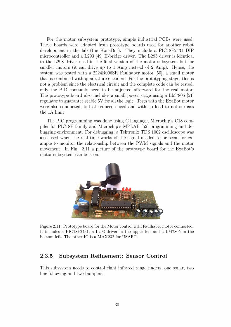
For the motor subsystem prototype, simple industrial PCBs were used.These boards were adapted from prototype boards used for another robotdevelopment in the lab (the KonaBot). They include a PIC18F2431 DIPmicrocontroller and a L293 [49] H-bridge driver. The L293 driver is identicalto the L298 driver used in the final version of the motor subsystem but forsmaller motors (it can drive up to 1 Amp instead of 2 Amp). Hence, thesystem was tested with a 2224R006SR Faulhaber motor [50], a small motorthat is combined with quadrature encoders. For the prototyping stage, this isnot a problem since the electrical circuit and the complete code can be tested,only the PID constants need to be adjusted afterward for the real motor.The prototype board also includes a small power stage using a LM7805 [51]regulator to guarantee stable 5V for all the logic. Tests with the ExaBot motorwere also conducted, but at reduced speed and with no load to not surpassthe 1A limit.
The PIC programming was done using C language, Microchip’s C18 com-piler for PIC18F family and Microchip’s MPLAB [52] programming and de-bugging environment. For debugging, a Tektronix TDS 1002 oscilloscope wasalso used when the real time works of the signal needed to be seen, for ex-ample to monitor the relationship between the PWM signals and the motormovement. In Fig. 2.11 a picture of the prototype board for the ExaBot’smotor subsystem can be seen.
Figure 2.11: Prototype board for the Motor control with Faulhaber motor connected.It includes a PIC18F2431, a L293 driver in the upper left and a LM7805 in thebottom left. The other IC is a MAX232 for USART.
2.3.5 Subsystem Refinement: Sensor Control
This subsystem needs to control eight infrared range finders, one sonar, twoline-following and two bumpers.
30

Hardware
In this subsection, the needed hardware to control each type of sensor will bedescribed.
Infrared range finders The chosen infrared range finders are the SharpGP2D120. As can be seen in the data sheet, this sensor has three pins: Vcc,Gnd and Vout. The timing diagram shows that measures are given every 38± 9.6 ms after power is supplied in the Vcc pin (see Fig. 2.12) [38].
Figure 2.12: Infrared range finder timing diagram.
The output is an analog voltage between 0 and 3.1V that is a function ofthe measured distance (see Fig. 2.13).
Figure 2.13: Infrared range finder analog output voltage vs distance to reflectiveobject.
In order to get the distance measurements, the analog output has to besensed in the middle of the output period (when the signal is stable), digital-ized and then- using the inverse of the transfer function- translated to distancein cm. The simplest way to achieve this algorithm is to program a microcon-troller, a device of the PIC18F family. The requirements for this part are that
31

the microcontroller has one timer- to trigger the range finders and sense theoutput at the appropriate time-, 8 digital pins to trigger each range finder,8 analog pins to get the output voltage of each range finder and at least oneanalog/Digital Converter (ADC) module to digitalize the analog output.
Moreover, since the typical consumption of the range finders is 45 mA andthe typical PIC pin can only drive 15 mA, the digital trigger pin cannot drivethe range finder directly. Hence, a driver is needed. A simple way to createsuch a driver is to use a transistor working as a switch. The transistor enablescurrent to go from the battery (emitter) to the range finder (collector) whenthe trigger pin (base) goes low.
Sonar The SRF05 sonar has four pins: Gnd, Vcc, Trigger Input and EchoOutput. First, a 10µs pulse to the trigger input needs to be provided to startthe measuring. When the sonar sends the ultrasonic burst, it raises the echooutput until it receives an echo from some object. The echo line is therefore apulse whose width is proportional to the distance to the object. By timing thepulse it is possible to calculate the range in centimeters: if the width of thepulse is measured in us, then dividing by 58 will give the distance in cm. Ifnothing is detected then the SRF05 will lower its echo line anyway after about30mS. The sonar can be triggered every 50 ms (i.e, 20 times per second).Figure 2.14 shows the timing diagram for the sonar.
Figure 2.14: Sonar Timing Diagram
The requirements for the microcontroller in this case are two digital pins(one for the trigger and another for the echo), a timer to produce the 10 µstrigger and some way to measure the time the echo line is up. Several PICshave a special Capture module to do exactly this, so one of such modules isrequired. In this case, the trigger and the Vcc are different lines, so althoughthe Sonar can sink up to 30 mA, these don’t need to be driven by the PICpin: they are drawn directly from the battery through the Vcc line. Hence,no extra driver is needed.
Line-following and Bumpers The two line following have three pins:
32

Vcc, Gnd and Out. The Out line has a digital one (5V) when it is seeing awhite line, and a digital zero (0V) otherwise. The bumpers have only two pins:when it is pressed, it joins both pins. Hence, they way to make it work is toconnect one of the pins to Vcc (likewise, Gnd) and the other one to the PICpin with a pull-down (likewise, pull-up). In this manner, when the bumper isnot pressed the PIC line has a digital zero and when it is pressed, the line hasa digital one.
To get a reading from this sensors, one way is to connect the out pin to aninterrupt-on-change pin in the microcontroller. As it is clear from the name ofthe pin, this hardware module in the microcontroller generates an interruptionwhen the input value changes. However, it is hard to get a microcontrollerwith 4 such pins. Another possibility is to poll the value of the pins at aregular interval. In this manner, the requirement for the microcontroller is tohave 4 digital inputs, 2 digital outputs for the trigger of the line-following (thebumpers are simply a switch so they don´t need a trigger), and a timer totrigger the polling.
The total requirements for the microcontroller (only to control the sensors)are: 8 analog pins, 16 digital pins, 2 timers, an ADC module and a Capturemodule. From the PIC18F family, the PIC18F4680 device features all this, soit is a clear candidate. This is a 44 pin microcontroller, differently from the 28pin PIC18F2431 used for motor control. Figure 2.15 shows a diagram of themain ICs and connections on this subsystem.
Figure 2.15: Sensor subsystem diagram
Software
An important feature of sensor control is that each sensor can be turned on oroff by software. There are special high-level commands so that only the sensorsthat are going to be used for the particular application are sensed. This follows
33

the Reconfigurability Requirement, enabling also important savings in energy-and hence in battery time-, always a sensible issue for an autonomous robot.
Infrared range finder Control Following the timing diagram in Fig.2.12, the output of the range finder is stable for sure between 38.3 + 9.6 + 5 =52.9ms and (38.3−9.6+0)∗2 = 57.4 ms after it has been first triggered. Hence,a timer needs to be set so that each range finder is put to A/D conversion 56 msafter it has been triggered. Since the PIC18F4680 has only one ADC module,a round-robin algorithm was implemented to capture the value of each rangefinder at a time. The timer was set to 28 ms, so that two range finders areon at all times and each range finder is ready for capture after two timerinterruptions. This yields a throughput of one new range finder value every 28ms. When the range finder is ready for capture, the ADC module starts theconversion, and interrupts the microcontroller when it finishes digitalizing thevalue. At that time, the result is stored and the range finder is turned off. Inthe current code version, the translation between the digitalized range findervalue and the distance in cm is implemented in the high-level processing unit,following the transfer function of Fig. 2.13. It is important to note that, inthe case of infrared range finders, the ability to turn off unused sensors ensuresthat the range finders that are in use are sensed more frequently.
For programming details see the PIC18F4680 data sheet [53], chapter 11 forTMR0 module, chapter 19 for the ADC module and chapter 9 for Interrupts.
Sonar Control The sonar trigger is controlled by the TMR1 timer module.This timer is first set to 100 µs to ensure the trigger line of the sonar is raisedfor that time. Then it is set to 50 ms to ensure the CCP module has captureda new echo value, and that the sonar is ready for a new trigger as specified bythe sonar data sheet.
The sonar capture is controlled by the Capture/Compare/PWM (CCP)module. This module in its Capture mode works with an associated timer,in this case TMR3. The module captures the TMR3 value and produces aninterrupt when a specified change in the capture pin occurs (for example,falling or raising edge). In this case, the capture pin of the CCP is connectedto the echo line of the sonar. Figure 2.16 presents a sequence diagram withthe interactions between the different PIC modules to achieve sonar control.For programming details see the PIC18F4680 data sheet [53], chapter 12 forTMR1, chapter 14 for TMR3 module, chapter 15 for CCP module and chapter9 for Interrupts.
Line Following and Bumper Control The Out lines of the two line-following and the two bumpers are connected to digital pins in the PIC. Thesoftware to control these sensors is simply polling: if they are on, once in everymain control cycle, each pin is polled to check the corresponding sensor value.
34

Sonar ControlInterruptModule
TMR1 CCP ModuleMain
alt
[int from TMR1]
[int from CCP]
alt
[trigger_start = true]
[else]
alt
[starting_capture]
[ending_capture]
alt
[sonar_new_result == true]
sonar_trigger()
trigger_start= :false
start_trigger()
set_timer(100us)
reset_TMR3()
stop_trigger()
set_timer(50ms)
trigger_start= :true
sonar_capture()
ini_time= read() :TMR3_captured_val
capture_timer_on_falling_edge()
end_time= read() :TMR3_captured_val
capture_timer_on_raising_edge()
sonar_new_result= set() :true
sonar_result= calculate() :end_time - ini_time
sonar_new_result= :false
Figure 2.16: Sequence diagram showing the interaction of the different modules toachieve Sonar control
Prototyping
To prototype the sensor subsystem, a simple industrial PCBs was adaptedfrom a prototype board used for a previous robot development in the lab (the
35

FenBot). This include a PIC18F248 DIP microcontroller, a similar controlleras the PIC18F4680 that includes all the necessary modules to test (CCP, ADCand timers), but it is smaller (only 28 pins) and hence simpler to route. Inthis board, the complete range finder acquisition was tested with one rangefinder (so one transistor was included), and the round-robin ring algorithmwith 3 triggers. The sonar, line-following and bumper code was also tested,as well as the SPI communication (as described in section 2.3.7). In thiscase, the prototype board did not include a power subsystem, so the 5V wereregulated externally using a Kenwood PR18-12 regulated DC power supply.As in the motor subsystem, the PIC programming was done using C language,Microchip’s C18 compiler and MPLAB environment, and the oscilloscope wasused for debugging real time signals. In Fig. 2.17 the prototype board for theExaBot’s sensor subsystem can be seen.
Figure 2.17: Prototype board for the Sensor control with a GP2D120 range finderconnected. The cables for SPI communication can be seen in the right, the ones forVcc and Gnd in the left.
2.3.6 Subsystem Integration
In the following subsections, the integration of the previous subsystems and thedevelopment and testing of the final embedded system is described followingthe methodology of subsection 2.2.4. First the three service subsystems aredescribed: Communication in subsection 2.3.7, Programming in subsection2.3.8 and Power in subsection 2.3.9. Finally, subsection 2.3.10 describes thefinal design and test of the PCB.
36

2.3.7 Subsystem Integration: Communication
In this subsection, the communication in the two main processing configura-tions is described, i.e., with or without the embedded PC104.
Hardware
The SPI bus has 4 wires: SS (Slave Select), MOSI (Master Out Slave In),MISO (Master In Slave Out) and SCLK (Slave Clock). Fig. 2.18 shows thetypical connections between one master and three slaves. The master alwaysstarts the communication, selecting the slave it wants to talk to by driving theappropriate SS pin low and generating the communication clock in the SCLKpin. The SPI bus is full-duplex: the SPI master gets one bit from the slave atthe same time it transmits one. Moreover, this is the only way a master canget information from the slave, by transmitting some data.
Figure 2.18: Typical configuration of SPI bus for one master and three slaves
Configuration with the PC104
The configuration shown in Fig. 2.18 is exactly how the PC104 (master)is connected to the three PICs (slaves). At first glance, nothing more thanthe appropriate wires between the pins are needed from the hardware point ofview. However, there are some details. One problem is that the PC104 uses3.3 V in the SPI pins, while the PIC uses 5V. This is not a big problem withthe communication from the PC104 to the PIC- since the logic 1 in almost allPIC pins is from 2.5V up, and hence 3.3V is read as a logic 15. However, it canbe a serious problem in the communication from the PICs to the PC104, sinceits pins are not prepared for higher than 3.3V voltages. Hence, a CD4050B[54] IC was included to convert the 5V of the PIC MISO lines into 3.3V.
5A “cute” detail is that just so happens that the SDI (or MOSI) pin in the PIC18F2431is one of the very few pins in which this is NOT true, so a pull-up had to be included totake the voltage slightly up for the communication to work. This was discovered after theproduction of the PCBs, so an adhoc pull up had to be added to the final board.
37
Another problem is that the SS pin of the PIC18F4680 is also the analogpin AN4. The issue is that the analog pins cannot be selected independentlyof the rest. For example, in order to use AN5, AN1-4 must be set as analogpins. Hence, overriding AN4 to be used as SS pin would mean that only AN1-3 can be used. This is not enough analog pins to control the 8 range findersand 2 line-following. To solve the problem, we used the SS pin as AN4, andconnected the slave select wire to the external interrupt pin (INT0). An extramodule and interrupt had to be configured and programmed, and hence theslave SPI code in the PIC18F4680 is different from the one in the other PICs.
Finally, the reset line of all three PICs are driven by the PC104, so that thePICs are taken out of reset after the PC104 is ready to start communication.
Configuration without the PC104
As already stated, it is desirable that the PC104 may be replaced by someother processing unit or taken away completely. This poses the need to putin all the electronics so that one of the three PICs can be the master of theSPI communication. Moreover, this PIC needs to communicate to an externalprocessing unit by a more common communication protocol, such as USART.In the PIC18F2431, the SPI pins overlap with the USART pins, so both cannotbe implemented at the same time. Hence, the PIC18F4680 takes up the masterspot in this configuration, implementing both the SPI master communicationand the USART communication.
Several jumpers need to be included to reconnect the MOSI/MISO, SlaveSelect and Reset lines. When the PIC18F4680 is a slave, its communicationoutput line is connected to the input line of the master. When it is the master,it’s output line needs to be connected to the input line of the other PICs. Theslave select and reset lines suffer a similar fate, since they need to be drivenby the PIC18F4680 instead of the PC104. For the RS232 communication,although the PIC has a module to produce the appropriate USART protocol,a MAX232 [55] driver was included to translate between the -11,+11V RS232voltage range and the PIC’s 0-5V voltage range.
Software
The developed communication protocol follows the Open System Interconnec-tion (OSI) model, implementing some of its seven layers. In the master ofthe communication, Physical, Data Link, Network and Application layers areimplemented. Since the slaves never start the communication, the networklayer is not needed and hence not implemented in the slaves.
Configuration with the PC104
Code in the SPI Master (PC104)
38

Physical layer: The SPI physical module in the PC104 implements twoindependent receive and transmit FIFOs that can be configured to hold up toeight words of 1 or 2 bytes each. It can be configured to work with interruptionsor polling. The Slave Selects are managed separately through the Digital InputOutput pins. Three DIO pins are connected to the three PIC slaves.
Link layer : The link layer packet sizes have an upper limit that is givenby the SPI physical buffers, which can hold up to eight words of 1 or 2 bytes.Since the SPI physical modules in the PICs can hold up to one byte, the SPIwords were set to 1 byte long. The packet size is of course reconfigurable. Inthe current code it is set to four bytes.
Network layer : The network protocol is implemented in the PC104 andmanages the reception and sending of packets to the three slaves. For each slaveit stores two buffers: one for received packets and another one for packets thatneed to be sent. The dispatching routine implements a round-robin algorithmthat runs every 10 ms, sending and receiving packets from each slave at a time.Figure 2.19 shows the interactions between network, link and physical layers toimplement this dispatching routine. The net layer exports read packet() andsend packet() functions that actually copy packets from/to the correspondingreception and sending buffers. The network layer packet formats can be seenin Table 2.3.
Application layer : A library is implemented to abstract the SPI and net-work communication details from a user application. For one, the libraryimplements the decoding of sensor data and encoding of commands, followingthe network layer packet format (see Table 2.3), and using the read packet()/ send packet() functions exported by the network layer. Since to receivedata from a slave the SPI master needs to send data, the library thread regu-larly sends a packet to every slave -containing commands or dummy data-to get an answer (e.g., to get the latest sensor readings). This applica-tion library, called libexabot, exports the following functions: exa initialize(),exa deinitialize(), exa set motors(), exa set sensors(), exa reset odometry(),exa receive(), exa IR distances(), exa sonar distance(). The last two func-tions implement the transformation of raw range finder and sonar measures todistance in cm as explained in subsection 2.3.5.
External communication In this configuration, communication with exter-nal PCs is done by Wi-Fi or cabled Ethernet. In both cases, the User Data-gram Protocol (UDP) was used. The preference of UDP over TCP for robotcontrol from an external PC comes from the fact TCP is connection-orientedand hence provides reliable ordered delivery of the stream of packets (evenif that means retransmitting and buffering packets). In contrast, UDP doesnot guarantee every packet is received, but sends packets as they are receivedand does not buffer or retransmit any information. As already discussed, inrobot control the timing of the commands and the return information is vi-
39

From To Information packet format
PC104 Sensor PICturn sensor on [0x01, sensor, U,U]turn sensor off [0x02, sensor, U,U]
Sensor PIC PC104 Sensor Info [sensor, val1, val2, val3]PC104 Motor PIC set velocity [0x10, vel, U,U]
Motor PIC PC104 odometry [0xf0, delta,countH, countL]
Table 2.3: Network layer packet formats. This can be extended if new sensors areadded. sensor: 0x00 : three left range finders, 0x01: three middle range finders,0x02, three right range finders, 0x03:sonar, 0x04: line-following, 0x05: bumper
tal. Receiving all commands together and late as would happen with a TCPconnection is far worse than eventually loosing some command because theUDP connection does not guarantee packet delivery. If the robot receives tencommands together, it will execute them all but in a late moment when theenvironment conditions may have already changed, making those commandsuseless or harmful. The UDP protocol is implemented using sockets, sharedmemory for the receiving and sending buffers and two threads: one for receiv-ing and a main thread that sends data back if required.
In total, three threads are running in the PC104 to complete communica-tion: one for the complete OSI stack of SPI, one for the UDP receive, and onefor the UDP send.
Code in the SPI Slaves
In the PICs, only the physical, link and application layers are implemented.In this case, the Physical SPI module has only a one-byte buffer for bothincoming and outcoming data, an hence lifts an interrupt when each byte isreceived.
Figure 2.20 shows a state machine diagram with typical interactions be-tween the different layers to implement the slave protocol. The state diagramshows the different states in the Link layer, including three of its internal vari-ables (receive and send buffers, and next byte to send). The transitions aregiven by the Physical layer interruptions when a byte is received PHY SPI ISR;and the calls from the Application layer to the two exported Link layer func-tions: SPI send packet and SPI receive packet. In any state, the applica-tion layer can call these link layer functions: when these transitions are notexplicitly drawn, the functions return false, and no transition is performed(i.e., no packet is copied from/to the link buffers).
In this state diagram, the reception starts when there is a packet to send.If there is no packet to send, then only dummy bytes are sent (depicted as D
in the diagram). Also, if a reception starts before a previous packet has beenread by the application, then the old packet is lost. That is why after receiving
40

Net Layer Link Layer Physical Layer DIOTimer
struct Slave { uchar send_buffer[MAX_PACKS*SIZE_PACK]; uchar send_count; //of packets uchar rcv_buffer[MAX_PACKS*SIZE_PACK]; uchar rcv_count; // of packets unsigned char dir_link; // DIO for the SPI Slave Sel. };
struct Net { slave slaves[SLAVES_QTY]; uchar lastSent; };
alt
[net.last_sent != None]
lastSL = net[slaves.last_sent]
loop
[phy_rcv_fifo is not empty]
alt
[nextSL != None]
loop
[copied bytes < size_packet]
Net Layer structures:
[every 10 ms]:net_admin()
deactivate(lastSL.dir_link)
DIO(last_SL.dir_link) = 1
receive_paq(lastSL.rcv_buffer)
lastSL.rcv_buffer[i]= read_byte(phy_rcv_fifo)
lastSL.rcv_count++()
nextSL= next_slave_with_packets_to_send()
activate(nextSL.dir_link)DIO(nextSL.dir_link) = 0
send_packet(nextSL.send_buffer)
send_FIFO.push(nextSL.send_buffer[i])
reorder(nextSL.send_buffer)
nextSL.send_count --()
net.last_sent = nextSL()
Figure 2.19: Sequence diagram showing the interactions between the different OSIlayers to implement the network protocol dispatching routine.
41

All empty
rcv_buffer = {D,D,D,D}snd_buffer = {D,D,D,D}byte_to_send = D
Ready to send
rcv_buffer = {D,D,D,D}snd_buffer = {b,c,d, D}byte_to_send = a
1st byte Received/Sent
rcv_buffer = {a',D,D,D}snd_buffer = {c,d,D, D}byte_to_send = b
2nd byte Received/Sent
rcv_buffer = {a',b',D,D}snd_buffer = {d,D,D, D}byte_to_send = c
3rd byte Received/Sent
rcv_buffer = {a',b',c',D}snd_buffer = {D,D,D,D}byte_to_send = d
Complete Packet
Received/Sent
rcv_buffer = {a',b',c',d'}snd_buffer = {D,D,D,D}byte_to_send = D
[PHY_SPI_isr(d')]/sent_byte = dnew_packet_rcvd =true
[SPI_receive_packet()]/return truercvd_packet={a',b',c',d'}new_packet_rcvd = false
[PHY_SPI_isr(c')]/sent_byte = c
[PHY_SPI_isr(b')]/sent_byte=b
[PHY_SPI_isr(a')]/sent_byte=a
[SPI_send_packet({a,b,c,d})]/return true
[SPI_receive_packet()]/return false
Figure 2.20: State Diagram showing a typical interaction of Phisycal, Link andApplication layers to send and receive a packet
the fourth byte of a packet, the link layer asserts the new packet rcvd flag.This flag performs the synchronization with the application layer: it is checkedin the main loop of each PIC. When it is asserted, the SPI receive packet
is called; and a new packet of data is sent using the SPI send packet.
There is one type of packet for the motor PICs, and six for the sensor PIC(see Fig. 2.3). The sensor PIC packets are sent back in turns; and only thepackets corresponding to the turned on sensors are sent back. Hence, if onlythe sonar is turned on, then all the packets from the sensor PIC include sonarvalues. Moreover, the last sensor data is sent.
Configuration without the PC104
When the PC104 is absent, the code for the SPI master is implemented inthe Sensor control PIC. This implementation follows the same link, applicationand network layer algorithms (i.e., the packet is four bytes long, the commandsare the same, and the round-robin network dispatching routine is the same).The changes reside in the physical layer- since the SPI physical module isdifferent in the PIC and in the PC104-, and in the way it is programmedIn the physical layer, the main difference is that the PIC has only one byteof physical buffer (for both reception and sending), and the PC104 has twoseparate reception and sending FIFO buffers. Since the link and networkalgorithms in the master are unchanged, the implementation in the slaves (i.e,the other two PICs) is also unchanged.
External communication In this configuration, communication with exter-nal PCs is done by cabled RS232. The Sensor PIC receives commands to turnon/off sensors and change motor speed, and redistributes those commands us-ing the SPI network. Regularly, it forms a packet with all the data from themotors and sensors, and sends that packet through the RS232 connection.
42

Prototyping
To prototype the communication subsystem, the prototype boards for thesensor and motor subsystem and the PC104 were connected. In order to testwith the PC104, a small perfboard with a DIP CD4050B and two connectorswas created to solve the 3.3V to 5V needed conversion. As in the other sub-systems, the PIC programming was done using C language, Microchip’s C18compiler and MPLAB environment, and the oscilloscope was used for debug-ging real-time signals. The PC104 was programmed in C using the availablecross-compilers. In Fig. 2.21 the connected prototype boards for the ExaBot’scommunication subsystem can be seen.
Figure 2.21: Prototype boards for communication subsystem. In this configuration,the prototype board of the Motor Control is connected to the PC104 through theperfboard with the CD4050B IC.
2.3.8 Subsystem Integration: Programming
The programming pins of each PIC are exported in a RJ45 connector. In thismanner, each of the three pics can be easily programmed in the final board.There are not many things to note about this subsystem. Since the Microchipprogrammer needs to manage the PIC resets when programming, a switch wasincluded for each PIC reset line to switch the control between the programmerand the SPI master. There is no special software for this subsystem. Theexistence of this subsystem is fundamental for the multiple code changes inthe ExaBot, due to its reconfigurable characteristics.
43

2.3.9 Subsystem Integration: Power
Once every sensor, actuator, IC and analog logic is defined, the exact require-ments for the battery and the power subsystem can be calculated. The firstconclusion from the previous sections is that there is need for two different reg-ulated voltages: 7,2V for the motors and 5V for the ICs and sensors. Hence,there are two separate batteries and power stages. The batteries used arerechargeable Lithium-Ion cells6. Each battery cell provides between 3,6V and4,2V, and its cappacity is 1,9 AmpH.
Motor power subsystem
Each motor needs regulated 7,2V and sinks a maximum of 2 Amp. To obtainthe regulated voltage, a minimum of 3 cells in series is needed. This also coversthe required current. To regulate to 7,2V for this kind of current, a LM350[56]regulator IC was used. This is a 3.0 Amp adjustable output (between 1.2Vand 33V) positive voltage regulator. Each motor has its own regulator, andthe adjustment to 7.2V is achieved with a variable resistance in the regulatorcircuit. Moreover, each motor has its own 3 Amp fuse in the event that themotor consumes more than the specified current.
Logic and sensors power subsystem
The logic and the sensors require regulated 5V. Since we are using a linearvoltage regulator, this means that the battery needs at least 2 cells in series.The amount of cells in parallel depend on the consumption of all the compo-nents. In table 2.4, typical and maximum consumption for all ICs (includingthe PC104) and sensors can be found. Initially, we built batteries with onlytwo cells (in series), since the calculated consumption was below the 1,9 AmpHcell capacity and this meant that the battery would last more than an hour.However, lately we are building batteries with 4 cells (two in parallel and twoin series), to get extra autonomy for longer experiments. A LM323 voltageregulator [57] was included. This is a 3 Amp, 5V positive voltage regulator,that is enough for the calculated consumption. A fuse was also included.
6Recently Lithium-ion polymer batteries have also been used.
44

Component typical max total typ. total max.PC104 450 450 450 450Sensor Subsys8 GP2D120 33 50 264 4001 SRF05 4 15 4 151 PIC4680 23 40 23 401 MAX232 8 10 8 10Total - - 316 465Motor Subsys2 L298 50 70 100 1402 ACS712 10 13 20 262 PIC2431 23 40 46 80Total - - 166 246Power Subsys2 LM350 3.5 10 7 201 LM323 12 20 12 20Total - - 19 40
Estimated Total 951 1201
Table 2.4: Typical and Maximum consumption rates of the main(i.e., most consum-ing) ICs and sensors to estimate the 5V battery requirements. All measures in mA.PICs running at 40 Mhz.
2.3.10 Subsystem Integration: Design and Test of thefinal PCB
Final Schematic Design
The final schematic was captured using Novram’s Diptrace, integrating theschematics for each of the subsystems and making the final changes.
An important feature in the final design is the inclusion of sensor expansionports. Although all the pins in the PIC18F4680 are used up, the two PICs thatcontrol the motors have several pins that are not used. In the final circuit, thepins needed for motor control were planned in those PICs in order to maximizethe possible applications of exported pins. In this way, the ExaBot has twoexpansion ports, each one exporting the following:
• one analog pin (to connect any analog sensor like infrared range finders,light sensors, etc)
• one CCP pin (Capture/Compare/PWM module like the one used tocontrol the sonar).
• a PWM pair (Pulse Width Modulation module, like the ones used to
45

control the motors).
• the INT0 pin (external interruption pin).
• GND and Vcc.
These expansion ports may prove a very powerful tool to add sensors and func-tionality to the ExaBot. The programming needed to control these added sen-sors can be done with the exported programming ports for each PIC18F2431
The final schematic for the complete board can be found in appendix A.This schematic has six sheets. The motor subsystem can be seen in sheetsmotor 1, motor 2 and motor flt; the sensor subsystem can be seen in sheetsensores, the communication subsystem in sheets con pc104 and sensores,the power subsystem in sheet power, and the programming subsystem in sheetcon pc104.
Final PCB routing
The complete schematic is exported to the PCB routing program and the fi-nal circuit is routed. The correct footprint for each final IC has to be used.Although there are several footprint libraries, many ICs do not have avail-able footprint so these have to be hand drawn respecting the exact packagedimensions. These can be found in the corresponding data sheet.
The space restrictions, the sensors and actuators spatial configuration needto be taken into account. Also, all the routing rules need to be followed. Someof these are: width of the path depending on the current, minimum distancebetween paths, or maximum angle in the paths. Other rules depend on thefunction of the signals, for example, all the paths that are in a bus need to haveroughly the same length so that the signals arrive approximately at the sametime (e.g., the clock and data paths in the SPI bus). Also heat dissipationneeds to be thought, for example with ground coating over unused parts ofthe board or with extra dissipation for over heating ICs (such as the voltageregulators). For details on this type of rules, see chapter 12 of [33]. The finalrouted board for the ExaBot has two layers and can be seen in appendix A.
Board production and testing
Before sending the board to production, it was peer reviewed and severalbugs were found. After production, all the ICs, resistances, transistors andcapacitors were soldered. Then, special code was programmed to electricallytest each pin of the board. In that phase, several bugs were found in thefinal circuit, luckily these bugs could be fixed and none required an additional
46

iteration of the board. However, these bugs form a list of known issues, thatneed to be fixed if a new iteration of boards is produced.
Software
The complete software has already been described in the subsystem refinementsections. At this point the complete software can be tested in the final board.For this, the code for each subsystem is tested separately, and in each subsys-tem every module is programmed and tested separately. Then, every moduleis integrated one by one testing that the previous capabilities are still valid.To program the code, Microchip’s MPLAB environment and C18 compiler wasused. For debug, apart from the PIC debugging capabilities, the Textronikoscilloscope and tester were also used.
2.3.11 Final Mounting
In the final mounting stage, the chassis was modified to mount all sensors, thefinal board and batteries. Moreover, all the cables were done. In Fig. 2.22three configurations of the final ExaBot can be seen.
(a) (b) (c) (d)
Figure 2.22: Four different configurations of the ExaBot: a) with all the sensorsand PC104 b) with a smart phone, c) with a netbook and a 3D Minoru Camera,d) with an embedded Mini-ITX board and a FireWire Camera
2.4 Applications
Different configurations of the ExaBot were used in several applications ful-filling all the goals the ExaBot was designed for. In this section we brieflycomment some of them.
47

2.4.1 Research: Autonomous visual navigation
The main research activities with the ExaBot are related to autonomous visualnavigation, both with monocular or 3D cameras.
An important work presents a new real-time image based monocular pathdetection method. It does not require camera calibration and works on semi-structured outdoor paths. The core of the method is based on segmentingimages and classifying each super-pixel to infer a contour of navigable space.To achieve real-time computation necessary for on-board execution in mo-bile robots, the image segmentation is implemented on a low-power embeddedGPU. For these experiments, the ExaBot was configured to use an embeddedMini-ITX board (AT5ION-T Deluxe) -that includes a 16 core NVIDIA GPU-as a main processing unit, and a firewire camera (model 21F04, from ImagingSource) as the only exteroperceptive sensor (see Fig. 2.22, image d). ThePC104 was taken away, and the AT5ION-T connects through RS232 to thePIC18F4680 as explained in section 2.3.7. This work was published in the pro-ceedings of the 18th Iberoamerican Congress on Pattern Recognition, CIARP2012 [58], and in the Journal of Real-Time Image Processing [59].
The same configuration of the ExaBot was used as the platform for all theexperiments in a completed PhD Thesis entitled “Vision-based mobile robotsystem for monocular navigation in indoor/outdoor environments”[60]. Thethesis proposes a hybrid method for navigation that combines the aforemen-tioned segmentation-based navigation method to follow paths, and a landmark-based navigation method to traverse open areas.
Another work presents the use of disparity maps for obstacle avoidanceusing two cameras. In this work, a common notebook or netbook is usedas a main processing unit and a cheap Minoru 3D USB webcam as the onlyexteroperceptive sensor. The notebook connects through cabled Ethernet tothe PC104, although the PC104 can be taken away if an appropriate convertorbetween USB and RS232 is provided for the notebook (see Fig. 2.22, image c).This work was published in the VII Jornadas Argentinas de Robotica, JAR2012 [61]. An extension of this work using elevation maps was presented inthe IEEE RAS Summer School on Robot Vision and Applications 2012 [62].
Two undergraduate students are doing their thesis on monocular visualodometry using as a main processing unit- and as the camera sensor- anAndroid-based smart-phone. This again presents a different configuration ofthe ExaBot (see Fig.2.22, image b). In this case, the Android cellphone con-nects through wi-fi to the on-board PC104. This is an ongoing work, the thesiswill probably be presented during April 2013.
Moreover, an undergraduate student is currently working on integrating aSICK TIM310 laser range finder to perform laser-based navigation. Finally,another student is integrating a compass sensor to perform sensor fusion with
48

the encoders and achieve a better localization estimation than pure encoder-based odometry. These works will be integrated in further autonomous navi-gation experiments.
2.4.2 Outreach
The ExaBot is also used in Educational Robotics courses, talks and visits. Ed-ucational Robotics proposes the use of robots as a teaching resource that allowsinexperienced students to approach fields other than specifically robotics. Overthe last years, Educational Robotics has grown substantially in elementary andhigh-school classrooms and also in outreach experiences to interest studentsin STEM7 undergraduate programs. A key problem is to have an adequateeasy-to-use interface between inexpert public and robots. Hence, one of thedevelopments of the lab is a new behavior-based application for programmingrobots, specially the ExaBot. Evaluation data on the application show thatover 90% of students find it easy to use. In Fig. 2.23 two snapshots of thisprogramming interface can be found.
a b
Figure 2.23: Easy Robot Behavior-Based Programming Interface: a) Main view. The upperpanel shows the main control functions: left: new, open, save. center: play, new timer, newcounter.right: close, b) A screen shot of the Braitenberg view. The left panel shows therobot schema and the transfer functions that can be used (top-down: inhibitory, excitatory,broken, constant). In the center of the work canvas all the sensors are shown (top-down: 2line-followings, 6 infrared telemeters, 1 sonar, 2 bumpers). The wheels are shown on eachside of the work canvas. The programmed behavior is a simple explorer that moves aroundat constant speed and can avoid obstacles
Robotic-centered courses and other outreach activities were designed andcarried on. In the last years, three eight-week courses, five two-days courses,more than ten one-day workshops and talks were taught to different high schoolstudents with the programming interface and several ExaBots. Also, the labparticipated in several big expositions such as ExpoUBA or INNOVAR. These
7Science, Technology, Engineering and Mathematics
49

activities are part of a comprehensive outreach program conducted by theExact and Natural Science Faculty of University of Buenos Aires, Argentina(FCEN-UBA). Statistical data show that since 2009 over 35% of new stu-dents at the FCEN-UBA had participated in some outreach activity, showinga significant impact of these activities in student enrollment at STEM-relatedcareers.
For this work, the ExaBot was configured with the PC104 as the mainprocessing unit and all the exteroperceptive sensors described in section 2.3.2:IR telemeters, sonar, bumpers and line-following (see Fig. 2.22, image a)These works resulted in one graduate thesis, and two papers: one in the 4thInternational Conference on Research and Education in Robotics [63] and amore complete one in the IEEE Transactions on Education Journal [64].
2.4.3 Undergraduate Education
The ExaBot is also used in undergraduate and graduate courses of the Departa-mento de Computacion, FCEN-UBA. In particular, it is used in the RoboticsVision course8. The course covers several topics on monocular 2D imagesand two cameras 3D images. Then, several algorithms for robot autonomousnavigation are programmed and tested using the ExaBot. This course hasbeen taught in two semesters during 2011 and 2012, and it is currently beingtaught. The ExaBot was also used in short lessons in other courses such asOrganizacion del Computador I, mainly to show microcontroller programmingguidelines.
2.5 Publications
In this section, the publications about the ExaBot and the papers using theExaBot are summarized.
We have published one journal article describing the ExaBot architecture,and also two short papers in conferences:
• 2010 A mobile mini robot architecture for research, education and pop-ularization of science, Sol Pedre, Pablo de Cristoforis, Javier Caccavelliand Andres Stoliar, Journal of Applied Computer Science Methods,Guest Editors: Jacek Zurada and Pablo Estevez, vol 2, no 1 pp 41-59,ISSN 1689-9636.
• 2009 ExaBot: a mini robot for research, education and popularization ofscience, Pablo De Cristoforis, Sol Pedre, Javier Caccavelli and Andres
8see the course webpage http://www-2.dc.uba.ar/materias/visrob/
50

Stoliar. Poster in VI Latin American Summer School in ComputationalIntelligence and Robotics - EVIC2009, Santiago, Chile, December 2009.Third price in poster contest.
• 2008 Exabot: un robot para divulgacion, docencia e investigacion, PabloDe Cristoforis, Sol Pedre y Juan Santos. Short communication in VJornadas Argentinas de Robotica – JAR08, Bahıa Blanca, Argentina,November 2008.
The ExaBot was also used as a robotic platform for experiments in twojournal papers, three conference papers and one poster:
• 2013 Real-time monocular image based path detection, Pablo de Cristoforis,Matıas Nitsche, Tomas Krajnık and Marta Mejail. Journal of Real TimeImage Processing, Springer Berlin Heidelberg, ISSN 0018-9162. In press,to appear may-june 2013.
• 2013 A Behavior-Based approach for educational robotics activities, Pablode Cristoforis, Sol Pedre, Matıas Nitsche, Thomas Fischer, Facundo Pes-sacg, Carlos Di Pietro, vol. 56, number 1, pp 61-66, IEEE Transactionson Education, ISSN 0018-9359.
• 2012 Stereo vision obstacle avoidance using disparity and elevation maps,Taihu Pire, Pablo de Cristoforis, Matıas Nitsche and Julio Jacobo Berlles,IEEE RAS Summer School on Robot Vision and Applications, Santiago,Chile. December 2012. (Poster)
• 2012 Real-Time On-Board Image Processing Using an Embedded GPUfor Monocular Vision-Based Navigation, Matıas Nitsche and Pablo deCristoforis, 18th Congress of Iberoamerican Pattern Recognition, CIARP2012, Buenos Aires, Argentina. Lecture Notes in Computer Science,Springer Berlin Heidelberg, vol 7441, pp 591-598.
• 2012 Evasion de obstaculos en tiempo real usando vision estereo, TaihuPire, VII Jornadas Argentinas de Robotica - JAR12, Olavarrıa, Ar-gentina, November 2012.
• 2011 A new programming interface for Educational Robotics, JavierCaccavelli, Sol Pedre, Pablo de Cristoforis, Andrea Katz and DiegoBendersky, 4th International Conference on Research and Education inRobotics, EUROBOT 2011. Prague, Czech Republic. Communicationsin Computer and Information Science, Springer Berlin Heidelberg, vol161, pp 68-77, ISSN 1865-0929.
51

2.6 Conclusions
In this chapter, we described the co-design of a control embedded system ap-plying the traditional flow in which processors and off-the-shelve ICs are com-bined: the development of the mini-robot ExaBot. This system has stringentreal-time, power consumption and size requirements, providing a challengingcase study.
To successfully design and build the robot prototype, the traditional co-design flow was adapted to the autonomous robotics field. The resulting flowhas six stages, starting from the robot’s goal definition, going through sub-system partition and refinement, all the way to the final mounting. All thisstages were applied to develop the robot prototype, and are described in detailin this chapter. The main goal for pursuing this task was to obtain a low-costrobot- i.e., ten times cheaper than commercially available research robots- thatcould be used not only for research, but also for outreach activities and edu-cation. In this sense, neither the commercially available research robots northe commercially available educational robots were a suitable solution.
The main requirement to achieve a low cost robot that could be used forsuch diverse fields was that the robot is highly reconfigurable. Hence, theExaBot was designed with many sensors and built-in sensor expansion ports.Also, the high level processing unit is reconfigurable. So far, the ExaBotwas used in four main configurations in our lab: with the PC104 and mostsensors for Educational Robotics activities; with a netbook/notebook and theMinoru Camera; with an embedded GPU and different cameras; and with anAndroid-based smart phone.
Six ExaBot robots are currently in use in the Laboratorio de Robotica ySistemas Embebidos of the FCEN-UBA. They have been used for educationalrobotics activities for high school students, research experiments in mobilerobotics, and education in graduate and undergraduate university courses. Inthe Educational Robotics field, robotic-centered courses and other outreachactivities were designed and carried on. In the last years, three eight-weekcourses, five two-days courses, and more than ten one-day workshops and talkswere taught to different high school students, using the ERBPI programminginterface developed in our lab and several ExaBots. The ExaBot is also used ingraduate and undergraduate courses at the Departamento de Computacion,FCEN-UBA. Finally, the ExaBot is used for research activities at our lab,mainly in vision-based autonomous navigation. It has been used to makeexperiments in one finished and two ongoing PhD thesis; and in three finishedand two ongoing graduate thesis. In this manner, the ExaBot was the platformused for experiments in two journal articles, three conference articles and oneposter.
52

Chapter 3
Embedded Systems usingFPGAs
Real-time hotspot detection
Some embedded systems require massive data processing with real-time con-straints that cannot be met with the standard microprocessor and IC approach.Examples include digital signal processing methods such as image, video or au-dio processing, and their applications to robotics, remote sensing, consumerelectronics among many other fields. In these cases, solutions based on FieldProgrammable Gate Arrays (FPGAs) or the design of particular ASICs (Ap-plication Specific Integrated Circuits) are common. These approaches takeadvantage of the inherent parallelism of many data processing algorithms andallow to create massive parallel solutions. They also allow tailored hardwareacceleration, e.g., with particular memory access patterns or bit tailored mul-tipliers/adders. ASICs provide the best solution in terms of performance,unit cost and power consumption. FPGAs are designed to be configured bya designer after manufacturing- hence “field-programmable”. The ability toupdate the functionality after shipping, partial re-configuration of a portion ofthe design, and the lower non-recurring engineering costs and shorter time-to-market compared to an ASIC design, offer advantages for many applications.According to the 2012 Embedded Market Survey, 35% of the surveyed engi-neers are currently using FPGAs in their designs [13].
In this chapter we introduce a traditional FPGA design flow and applyit to a remote sensing application that requires massive data processing withreal-time constraints [21]. The main contributions in this chapter are:
• The introduction of a traditional FPGA design flow, derived from theanalysis of design flows presented in several foundational FPGA books.A short comparison with those design flows is also presented. Also, prosand cons of this type of design flows are discussed, based on bibliograph-
53

ical research and our own experience.
• The proposal of a novel algorithm to segment real-time video from aninfrared camera on an UAV (Unmanned Aerial Vehicle) in order to findthe location and spatial configuration of hot spots present in each frame.To process each pixel, the algorithm only uses the information of the pre-vious line of pixels, enabling a parallel implementation that can processthe image as it is being acquired to meet tight real-time constraints.
• The implementation of this algorithm following the presented traditionalFPGA design flow. The FPGA solution takes the analogical output ofan IR camera, process the frames in real-time and sends the informa-tion of found hotspots in Ethernet packets. The implemented solutionsuccessfully segments the image with a total processing delay equal tothe acquisition time of one pixel (that is, at video rate). The processingdelay is independent of the image size. Sizing equations are presented,and timing, area and power results are discussed.
This chapter is organized as follows. Section 3.1 introduces FPGAs, in-cluding their field of application and importance, while section 3.2 presents adescription of FPGA basic architecture. Section 3.3 introduces the traditionalFPGA design flow. In section 3.4, this flow is applied to obtain a real-timehot spot detection using FPGA for the UAV application. Finally, discussionand conclusions are presented in section 3.5.
3.1 Introduction
The concepts of this section are mostly taken from three important books ofFPGA design: Wayne Wolf’s “FPGA-Based Design” [6], Clive Maxfield’s “TheDesign Warrior’s Guide to FPGAs” [1] and Cofer and Harding’s book “RapidSystem Prototyping with FPGAs” [2]. Other works are cited as required.
3.1.1 What is an FPGA?
Field programmable gate arrays (FPGAs) are digital integrated circuits (ICs)that contain configurable (programmable) blocks of logic along with config-urable interconnects between these blocks. Design engineers can configure(program) such devices to perform a tremendous variety of tasks. The “fieldprogrammable” portion of the FPGA’s name refers to the fact that its pro-gramming takes place “in the field” (as opposed to devices whose internalfunctionality is hardwired by the manufacturer). This may mean that FPGAsare configured in the laboratory, or it may refer to modifying the function of a
54

device resident in an electronic system that has already been deployed in theoutside world.
3.1.2 Why are FPGAs of interest?
Some embedded systems require massive data processing with real-time con-straints that cannot be met with the standard microprocessor and IC approach.In these cases, solutions based on Field Programmable Gate Arrays (FPGAs)or the design of ASICs (Application Specific Integrated Circuits) are common.
Nowadays FPGAs contain million of logic gates and can be used to imple-ment extremely large and complex functions that previously could be realizedonly using ASICs. The cost of an FPGA design is much lower than that ofan ASIC (although the ensuing ASIC components are much cheaper in largeproduction runs). At the same time, implementing design changes is much eas-ier in FPGAs, and the time-to-market for such designs is much faster. Thus,FPGAs make a lot of small, innovative design companies viable because- inaddition to their use by large system design houses- FPGAs facilitate “Fred-in-the-shed”-type operations. This means they allow individual engineers orsmall groups of engineers to realize their hardware and software concepts onan FPGA-based test platform without having to incur the enormous nonre-curring engineering (NRE) costs or purchase the expensive toolsets associatedwith ASIC designs.
These advantages are of particular interest in countries like Argentina.Nowadays, Argentina has no capabilities for manufacturing complete ASICs,and the initial cost for such designs make them prohibitively for small start-ups. FPGAs offer the possibility for national small companies to design andimplement products that are adequate for our reality, or that could even re-place imported products (given appropriate state policies). These not onlyinclude possibilities for design companies, but also for functional and formalverification start-ups that could verify those designs (and others). There arealready some companies in Argentina developing with FPGAs, such as INVAP[65]. INVAP [65].
3.1.3 What are FPGAs used for?
When they first arrived on the scene in the mid-1980s, FPGAs were largelyused to implement glue logic, medium-complexity state machines, and rela-tively limited data processing tasks. During the early 1990s, as the size andsophistication of FPGAs started to increase, their big markets at that timewere in the telecommunications and networking arenas, both of which involvedprocessing large blocks of data and moving that data around.
55

Later, toward the end of the 1990s, the use of FPGAs in consumer, auto-motive, and industrial applications underwent a very big growth. FPGAs were(and still are) often used to prototype ASIC designs or to provide a hardwareplatform on which to verify the physical implementation of new algorithms.However, their low development cost and short time-to-market made them toincreasingly find their way into final products.
By the early-2000s, high-performance FPGAs containing millions of gatesbecame available. Some of these devices feature embedded microprocessorcores, high-speed input/output (I/O) interfaces, and the like. The end result isthat today’s FPGAs can be used to implement just about anything, includingcommunications devices and software-defined radios; radar, image, and otherdigital signal processing (DSP) applications; all the way up to system-on-chip(SoC) components that contain both hardware and software elements.
FPGAs are currently growing into three major market segments: ASIC andcustom silicon, Digital Signal Processing, and physical layer communicationchips. Furthermore, FPGAs have created a new market in their own right:reconfigurable computing.
By 2010, FPGAs comprised a 4 billion dollar market, with leading appli-cations in communications and industry [66]. Fig. 3.1 shows the distributionof FPGA market by end applications [67].
Figure 3.1: FPGA market by end application
Moreover, FPGA vendors offer particular families for different end appli-cation. For example, Xilinx offer families and solutions for applications inAerospace and Defense, ASIC Prototyping, Audio, Automotive, ConsumerElectronics, Data Center and several others (See [68]).
56

3.2 FPGA Basic Architecture
FPGA devices are based on a number of common configurable structures.While there are minor and major variations in the implementation of thesestructures between manufacturers and device families, the structures are com-mon to almost all mainstream FPGA devices. The fundamental FPGA struc-tures are:
• Logic Blocks
• Routing Matrix & Global Signals
• I/O Blocks
• Clock Resources
• Memory
• Multipliers, Adders, DPS blocks.
• Advanced Features (e.g, hard embedded processors).
In following sections we briefly describe this structures. Most of the con-cepts of this section are taken from [1] and [2].
3.2.1 Logic Blocks
FPGA logic blocks may have different architectures within different families,even if they are from the same manufacturer. Each manufacturer tends to callthe lowest-level FPGA logic block by different names, e.g. logic cell (Xilinx)or logic element (Altera). A logic block will typically contain one or more N-input look-up tables (LUTs) along with one or more flip-flops, signal routingmuxes, control signals and carry logic. In the advanced FPGA families, theinternal architecture of a logic block is often quite complicated.
Each LUT element can implement any Boolean function with N or fewerinputs. A majority of the implementations of LUT architectures have fourinputs; and allow LUTs to be also used as distributed memory or shift registers.Figure 3.2 shows a simplified Xilinx Logic Cell.
In order to support higher levels of functionality, logic blocks may begrouped together by the manufacturer, forming a larger structure. Some ex-ample names for these combined logic block groups are: tile, configurable logicblock (CLB) and logic array block (LAB). Fig. 3.3 shows a simplified array ofXilinx’s CLBs.
57

Figure 3.2: Simplified Xilinx Logic Cell (figure taken from [1])
Figure 3.3: Simplified Xilinx CLB, comprising 4 Slices of 2 Logic Cells each. (figuretaken from [1])
3.2.2 Routing Matrix & Global Signals
The fundamental routing elements for an FPGA are the horizontal/verticalrouting channels and programmable routing switches. The function of thehorizontal and vertical routing channels is to provide a connection mechanismbetween routing switches. The routing switch is programmable and can pro-vide either 180- or 90-degree routing path. Figure 3.4 shows a typical routingmatrix.
Another mechanism that FPGA employs for connecting both switches andCLBs is carry chain logic. Carry chain logic is commonly used to build largeefficient structures for implementing arithmetic functions within the generallogic fabric. Most manufacturers have also implemented global low-skew rout-ing resources. These resources are typically limited in quantity and shouldbe reserved for high-performance and high-load signals. Global routing re-sources are often used for clock and control signals, which tend to be bothhigh-performance and high-fanout.
58

Figure 3.4: FPGA routing signal (figure taken from [2])
3.2.3 I/O Blocks
The ring of I/O banks surrounding the array of CLBs is used to interfacethe FPGA device to external components. I/O block (IOB) is a common termused to describe an I/O structure. An IOB includes input and output registers,control signals, muxes and clock signals. Fig. 3.5 shows a generic I/O block
Figure 3.5: I/O block
In order to interface to different types of logic, I/O Blocks are highly config-urable. Possible configurations include direction (input, output, bidirectional),data rate (SDR, DDR, SERDES), I/O standard (single-ended, differential, ref-erenced, etc.) and I/O voltage (1.2 V to 3.3 V for single-ended standards).
59

3.2.4 Clock Resources
Clock Tree
All of the synchronous elements inside an FPGA need to be driven by a clocksignal. Such a clock signal typically originates in the outside world, comesinto the FPGA via a special clock input pin, and is then routed through thedevice and connected to the appropriate elements. Fig. 3.6 shows a simpleclock tree.
Figure 3.6: A simple clock tree (figure taken from [1]).
The clock tree is implemented using the special low-skew tracks and isseparate from the general-purpose programmable interconnect. Multiple clockpins are available (unused clock pins can be employed as general-purpose I/Opins), and there are multiple clock domains (clock trees) inside the device.
Clock Managers
Instead of configuring a clock pin to connect directly into an internal clocktree, that pin can be used to drive a special hard-wired function (block) calleda clock manager that generates a number of daughter clocks (Figure 3.7).
Clock Managers are used to generate daughter clocks with frequencies thatare derived by multiplying or dividing the original signal; and/or by phase-shifting it. They are also used to correct clock signals, for example by removingjitter or correcting the skew from generated daughter clocks.
3.2.5 Embedded Memory
A lot of applications require the use of memory, so FPGAs include relativelylarge blocks of embedded RAM called e-RAM or block RAM. Depending on
60

Figure 3.7: Clock Manager (figure taken from [1]).
the architecture of the component, these blocks might be positioned aroundthe periphery of the device, scattered across the face of the chip in relativeisolation, or organized in columns. Each block of RAM can be used inde-pendently, or multiple blocks can be combined together to implement largerblocks. These blocks can be used for a variety of purposes, such as implement-ing standard single- or dual-port RAMs, first-in first-out (FIFO) functions,state machines, etc. Fig. 3.8 shows the structure of a memory block.
Figure 3.8: Embedded memory block.
3.2.6 Multipliers, Adders, DPS blocks
Some functions, like multipliers, are inherently slow if they are implementedby connecting a large number of programmable logic blocks together. Sincethese functions are required by a lot of applications, many FPGAs incorporatespecial hardwired multiplier blocks. These are typically located in close prox-imity to the embedded RAM blocks because these functions are often used inconjunction with each other.
61

Similarly, some FPGAs offer dedicated adder blocks. One operation thatis very common in DSP-type applications is called a multiply-and-accumulate(MAC). This function multiplies two numbers together and adds the result toa running total stored in an accumulator. Nowadays’ FPGA offer DSP blocksthat typically implement 18×18 bit multiplier, 48 + 48 bit adder/accumulator,pre-adders for symmetric FIR filters and that can be dynamically configuredand highly pipelined (Figure 3.9).
Figure 3.9: Digital Signal Processing blocks
3.2.7 Advanced features
As FPGA devices and architectures continue to evolve, certain advanced struc-tures will be implemented in significantly different ways by different manu-facturers. Often these advanced FPGA structures and features are targetedtoward very specialized applications and technology specialties. Examples in-clude enhanced clock features, specialized Intellectual Property (IP) cores oradvanced I/O standards and protocol support.
Of special interest to this thesis are embedded processors, as referred innext chapter. FPGAs may contain one or more embedded microprocessors.These processors may be hard or soft processors. A hard microprocessor coreis implemented as a dedicated, predefined block. As opposed to embedding amicroprocessor physically into the fabric of the chip, it is possible to configurea group of programmable logic blocks to act as a microprocessor. These arecalled soft cores.
62

3.2.8 The complete picture
Fig. 3.10 shows a generic FPGA architecture including the described struc-tures.
Figure 3.10: Generic FPGA architecture (figure taken from [2])
3.3 Design Flows for FPGA
In this section, a standard FPGA design flow is presented. The concepts of thissection are taken from these books: Cofer and Harding’s “Rapid System Proto-typing with FPGAs” [2], Chu’s “FPGA Prototyping by VHDL Examples”[3],Maxfield’s “The Design Warrior’s Guide to FPGAs” [1], Wolf’s “FPGA-BasedSystem Design” [6] and Kilts’ “Advanced FPGA Design” [5]. The equivalenceof the presented flow with the exact ones showed in those books is presentedat the end of this section. It is important to point out that this is a genericFPGA design flow, it may vary according to the particular application area.
The high-level design phases associated with FPGA design include require-ments, architecture, implementation, and verification. The following descrip-tions provide some detail on the tasks which must be completed during theprimary design phases specified:
• Requirements Phase Define and detail the required functionality, in-terfaces, performance, and design margin. Develop and maintain a de-sign requirement specification.
63

• Architecture Phase Partition design into functional blocks, allocatefunctionality, and performance requirements. Define system architectureand design hierarchy. Determine which design components will imple-ment required functionality.
• Implementation Phase Code the design using a Hardware DescriptionLanguage (HDL), and then synthesize and place and route the design tothe particular FPGA. Several simulation steps can also be performed inthis stage to test the design.
• Verification Phase The design file that defines the state of every con-figurable element within the FPGA is “downloaded” to the part. Thisprocess is also referred to as “configuration’. Using external test equip-ment and access to internal nodes, the design’s functionality and real-world performance is verified.
In the next subsections two main phases of this flow are described: theArchitecture and Implementation Phases.
3.3.1 Architecture Phase
In this phase, the general architecture of the system is designed. The keyconcept in this phase is hierarchichal design.
Hierarchical design is a standard method for dealing with complex digitaldesigns. It is commonly used in programming: a method is written not as ahuge list of primitive statements but as calls to simpler methods. Each methodbreaks down the task into smaller operations until each step is refined into amethod simple enough to be written directly. This technique is commonlyknown as divide-and-conquer- the method’s complexity is conquered byrecursively breaking it down to manageable pieces.
In digital circuits, implementing an informed subsystem partition in a hi-erarchichal manner is an important method to increase a design’s ability toabsorb change, and decrease development time and complexity. In rapid de-velopment, individual design subsystems can be developed concurrently byisolated groups of specialists. This requires the development of individualblocks designed to specific requirements, allowing independent developmentand verification. Ideally, the modules should be designed so they are highlyindependent of one another. This can isolate risks associated with functionalimplementation and allow design modules to be updated with less disruptionto the rest of the design implementation. With a modular design approach,the design integration phase can also progress more smoothly if the individualmodules’ functionality and interfaces have been correctly defined, implementedand tested.
64

At this stage is important to consider a range of potential design imple-mentation approaches. High-level and detailed FPGA system block diagramand functional level block diagrams, including appropriate interface details,are very useful. It is important to keep in mind that decisions made at thisstage might influence requirements, and also that implementation details ofthe next phase might also change architecture. It is usual that partition isdone taking into account possible implementations of the modules down theline.
Critical elements in a modular design are timing and design block inter-faces.The selection of design boundaries can have significant effects on place-ment and routing and overall compilation efficiency. The following is a list ofpartitioning considerations to keep in mind:
• Group related functional blocks, or blocks that have many signals incommon. They have the greatest effect on the place-and-route process.
• Separate portions of the design that have different design goals (per-formance, area, etc.). This allows the designer to apply appropriatesynthesis directives to specific design blocks.
• Where possible, divide groups along boundaries where signals are regis-tered. Avoid assigning a boundary across combinatorial logic, since thiscan interfere with logic optimization.
3.3.2 Implementation Phase
In this phase, each module of the architecture design is refined, implemented,synthesized and simulated in an iterative manner until the module is function-ally correct and meets all the timing and performance goals. Then, all themodules are integrated and tested. Fig. 3.11 shows the stages in this phase.
HDL Capture
The design is captured using a Hardware Description Language, special lan-guages used to describe digital circuits. The functionality of a digital circuitcan be represented at different levels of abstraction (Fig. 3.12).
The lowest level is the switch level, which describes the circuit as a netlistof transistor switches. A slightly higher level of abstraction is the gate level,which describes is as a netlist of primitive logic gates and functions. Bothswitch-level and gate-level netlists may be classed as structural representa-tions.
65

Post PAR Timing
Simulation and
Analysis
HDL Capture
Logic Synthesis
Behavioral Simulation
Synthesis Constraints
I/O, Timing and Area
Constraints
Physical Implementation
Translate
Map
Place & Route
[constraintsNOT met]
Generate Bitsream
/Program Device
Gate Level
Architecture Analysis
& Timing simulation
[no changesneeded]
[need changesfor timingclosure]
[no changesneeded]
affect
[ need changesin gate-leveldesign/ timing ]
[no changes needed]
[need changes for correct behaviour]
affect
HDL code +Testbench
Figure 3.11: Activity diagram of the Implementation phase of FPGA design flow
The next level of HDL abstraction is functional representations. This in-cludes the description of functions using Boolean equations and also RegisterTransfer Level (RTL) representations. In RTL descriptions, the clocked be-havior of the design is expressly described in terms of data transfers betweenstorage elements in sequential logic (which may be implied) and combinatoriallogic (which may represent any computing or arithmetic-logic-unit logic). RTLdescriptions are said to be technology-independent (retargetable to differentdevice families), however, the architecture implied by the description is fixed 1.
The highest level of abstraction supported by traditional HDLs is knownas behavioral, that include constructs such as processes or loops. This usu-ally does not imply specific timing. Hence, Behavioral descriptions are usuallyarchitecture-independent : several RTL circuits can implement the same be-havioral description, but with different timing, area and power implications.Synthesis to gates, from a description at this level of abstraction, requires so-phisticated tools. To influence the design implementation made by synthesistools, synthesis constraints can be applied. However, there is only so mucha synthesis tool with appropriate constraints can do: to ensure a particular
1A detail on this is that some synthesis constraints can change the final implied architec-ture, e.g., the Register balancing constraint that is used to meet design timing requirementsby moving the placement of Boolean logic functionality across register boundaries
66

synthesized architecture, HDL software changes may be needed.
As a final comment, HDLs have a dual nature: they are not only usedfor implementation but can also be used for simulation. Hence, there areconstructs in HDL which are syntactically correct but are not synthesizableinto a design that can be placed in a targeted FPGA. The two most commonlyused HDLs are Verilog and VHDL.
Figure 3.12: VHDL and Verilog levels of abstraction
HDL coding guidelines and patterns
Coding guidelines and patterns in HDL are very important because theyimpact performance. One reason for this is that, although they might be log-ically equivalent, different RTL statements can yield different architectures.Also, tools are part of the equation because different tools can also yield dif-ferent results. Hence, when coding in HDL, two things are important:
• To design the desired underlying hardware architecture for the particulartiming, area and power constraints of the module.
• To know which HDL constructs will synthesize that architecture.
This makes the discussion of how to code in HDL intrinsically related to thediscussion of how to design the underlying digital circuit to achieve the requiretiming, area and power performance. It also makes HDL coding patterns, thatare known to synthesize particular architectures, very important.
Moreover, the ability of HDL to accurately describe the desired hardwarearchitecture can make HDL code very hard to understand, debug and main-tain. To describe the concurrent nature of hardware, HDL code usually in-cludes many low-level concurrent statements that become very difficult to un-derstand when the number of concurrent statements surpasses some small
67

amount. This makes bugs very hard to find. Hence, coding guidelines andpatterns are important not only to assure the desired hardware is synthesized,but also to enable understandable code among a variety of designers, a vitalpoint in moderate-to-big designs.
Complete books are written on HDL coding guidelines and patterns, soa detailed description is clearly out of scope of this thesis. However, it isimportant to point out some ideas to get a picture of the problem the workon this thesis aims to tackle. That is, that the growing complexity of digitalcircuits make it very difficult for designers to model the functional intent of thesystem and implement it using HDL languages and traditional FPGA designflows.
In following sections, the different types of circuits and very small amountof coding guidelines are presented. This design methodology together withcoding guidelines are taken from Pong P. Chu’s book “FPGA Prototyping byVHDL Examples” [3]2. General considerations are taken from [2] and [1].
General Considerations
Inference and Instantiation
As already stated, each RTL construct in HDL code synthesize to a par-ticular hardware structure. In order to design good and optimized circuits,it is very important to know what hardware is inferred when writing a par-ticular code. Another way to determine which particular hardware will beput in the resulting digital circuit is to instantiate a particular IP core thatwraps a physically existing resource in the FPGA (for example, a DSP blockor BRAM). Inference is preferred when the objective is design flexibility ordesign portability; instantiation when seeking to take the greatest advantageof architecture specific structures and architectural features.
Procedural and Structural Coding
Procedural and structural are two general coding styles:
• Procedural Coding Style: the “behavior” of a circuit is described in se-quential, top-to-bottom code, similar to the code implemented in proce-dural languages like C. Much procedural-style code is supported for RTLsynthesis, and does not require a behavioral synthesis tool, and for thatreason this style is usually referred to as behavioral code. In order fortools to understand top-to-bottom statements, they need to be wrappedin VHDL processes or Verilog always blocks.
• Structural : the structure of the circuit is explicitly written, including in-stantiating components and specifying which signals (nets, wires) are
2Chu also has this book in Verilog flavor, see [69]
68

connected to each pin of the component. It is similar to specifyingschematic connections explicitly in text.
It is possible for users to mix structural and procedural coding styles inthe same VHDL or Verilog source file. Procedural style code is easier to read,however, structural style code is typically used for instantiating technology-specific library cells (such as I/O pads), memory cells, third-party IP blocks,and lower-levels of the hierarchy from the HDL code. Structural code is alsoused to explicitly show parallel sections.
Types of circuits
Combinatorial circuits
A combinatorial circuit is a circuit in which the output is a function ofthe input only. Combinatorial circuits are important because they are thebuilding blocks of higher-level architectures. They include logical operators,arithmetic operators such as adders or multipliers, and relational operatorssuch as comparators. Also, routing circuits made with multiplexers, such aspriority or parallel routing. Guidelines for coding this combinatorial circuitscan be found in chapter 3 of [3].
Sequential circuits
A sequential circuit is a circuit with memory, which forms the internalstate of the circuit. Unlike a combinatorial circuit, in which the output is afunction of input only, the output of a sequential circuit is a function of theinput and the internal state.
Synchronous Design is the most commonly used practice in designing asequential circuit. In this method, all storage elements are controlled (i.e.,synchronized) by a global clock signal and the data is sampled and stored atthe rising or falling edge of the clock signal. It allows designers to separate thestorage components from the circuit and greatly simplifies the developmentprocess. It also simplifies design reuse, and timing simulation, static timinganalysis and constraints.
Figure 3.13: Block diagram of a synchronous system (figure taken from [3])
69
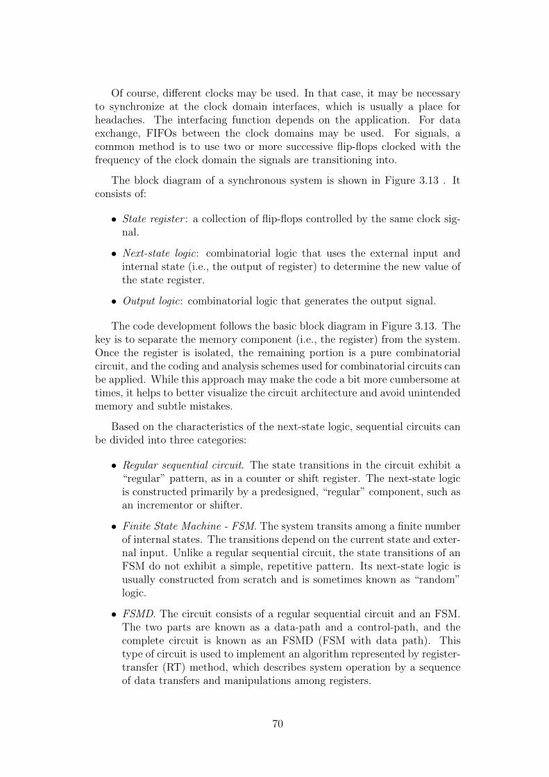
Of course, different clocks may be used. In that case, it may be necessaryto synchronize at the clock domain interfaces, which is usually a place forheadaches. The interfacing function depends on the application. For dataexchange, FIFOs between the clock domains may be used. For signals, acommon method is to use two or more successive flip-flops clocked with thefrequency of the clock domain the signals are transitioning into.
The block diagram of a synchronous system is shown in Figure 3.13 . Itconsists of:
• State register : a collection of flip-flops controlled by the same clock sig-nal.
• Next-state logic: combinatorial logic that uses the external input andinternal state (i.e., the output of register) to determine the new value ofthe state register.
• Output logic: combinatorial logic that generates the output signal.
The code development follows the basic block diagram in Figure 3.13. Thekey is to separate the memory component (i.e., the register) from the system.Once the register is isolated, the remaining portion is a pure combinatorialcircuit, and the coding and analysis schemes used for combinatorial circuits canbe applied. While this approach may make the code a bit more cumbersome attimes, it helps to better visualize the circuit architecture and avoid unintendedmemory and subtle mistakes.
Based on the characteristics of the next-state logic, sequential circuits canbe divided into three categories:
• Regular sequential circuit. The state transitions in the circuit exhibit a“regular” pattern, as in a counter or shift register. The next-state logicis constructed primarily by a predesigned, “regular” component, such asan incrementor or shifter.
• Finite State Machine - FSM. The system transits among a finite numberof internal states. The transitions depend on the current state and exter-nal input. Unlike a regular sequential circuit, the state transitions of anFSM do not exhibit a simple, repetitive pattern. Its next-state logic isusually constructed from scratch and is sometimes known as “random”logic.
• FSMD. The circuit consists of a regular sequential circuit and an FSM.The two parts are known as a data-path and a control-path, and thecomplete circuit is known as an FSMD (FSM with data path). Thistype of circuit is used to implement an algorithm represented by register-transfer (RT) method, which describes system operation by a sequenceof data transfers and manipulations among registers.
70

Sequential Circuits coding guidelines
In all the cases, the state register needs to be coded as a process. Theprocess has the clock and reset signals in the activation list, both signalsnecessary to synthesize memory.
The rest of the coding guidelines depend on the type of sequential circuit.
• Regular sequential circuits: the next-state and output logic can be codedas combinatorial circuits.
• FSMs: the next-state logic is coded as a process that has as activationsignals the previous state and the input signals. Inside the process, acase statement defines which is the next state for each current stateand inputs- i.e, it codes the FSM. The output logic is also coded asprocess that defines the output for each state. The activation signalsof this output logic process depend on the type of FSM. In Moore typemachines, the output depends only on the state and hence the activationsignal only includes the state. In the case of Mealy machines, it dependsboth on the state and the input signals; and hence both are in the process’activation list.
• FSMDs: this can be coded following the block diagram in 3.14. Oneprocess codes the state and data path registers, having clock and reset asactivation signals. Another processes codes the control path (next statelogic + control signals), having as activation signals the state registerand input signals. A third process codes the output signals. Finally, thedata path can be coded as a combinatorial circuit.
Of course, other coding patterns can be applied to code this circuits. De-tails con be found in chapter 4,5 and 6 of [3].
Optimizations
To close the HDL Capture section, a few words on optimization techniques.When talking of optimizations in FPGA design, there are several conflictinggoals:
• Performance: The logic must run at a required rate. Performance canbe measured in several ways, such as throughput and latency (usuallyconflicting among them). Clock rate is usually used as a measure ofperformance.
• Power/energy: The chip must often run within an energy or power bud-get. Energy consumption is clearly critical in battery-powered systems.
• Area: Area occupancy is usually related to the cost of the chip that willhost the design.
71

Figure 3.14: Block Diagram of a Data Path - Controller Architecture (figure takenfrom [3])
Although constraints for synthesis tools are useful to optimize designs inthese vectors, in this type of HDL coding, optimizations are mostly given bythe general architecture of the system and the designed hardware architectureof each module. There are many techniques to optimize designs in each ofthe mentioned topics. For example, pipelining is a very usual approach toincrease throughput. Resource sharing is very common for reducing area- butit usually decreases throughout. On the contrary, replicating hardware mod-ules can be used to increase throughput and decrease latency, but of course,increasing area. Although almost all FPGA design books include some sec-tion for optimizations, an excellent book on detailed optimizations techniquesis Steve Kilts’ “Advanced FPGA Design. Architecture, Implementation andOptimization” [5].
The above are usual performance goals taking into account only the designitself. However, at least two other goals must be taken into account:
• Design time: It cannot take forever to design and optimize the system.This means that actions need to be taken to reduce design and verifica-tion time.
• Design cost: Of course, design time affects costs. Another important costis tools: in FPGA design there are many very interesting tools that can
72

help with reducing design and verification time. However, many timesthis tools are prohibitively expensive3.
Logic synthesis
Logical synthesis is the process of translating an HDL language design descrip-tion into a pure RTL design description. The synthesis process occurs as asequence of stages. The first stage is the parsing of the HDL code for syntaxerrors. When the code is verified to be syntactically correct, the synthesis toolbegins the process of translating the design into an RTL description (registers,Boolean equations, clocks and interconnecting signals). The output of the syn-thesis process is a netlist file, which is used as an input to the place-and-routetools discussed in following subsection.
Physical implementation
The Physical process consists of three smaller processes: translate, map, andplace and route. The translate process merges multiple design files to a singlenetlist. The map process, which is generally known as technology mapping,maps the generic gates in the netlist to FPGAs logic cells and IOBs. Theplace and route process, which is generally known as placement and routing,derives the physical layout inside the FPGA chip. It places the cells in physicallocations and determines the routes to connect various signals. Static timinganalysis, which determines various timing parameters, such as maximal prop-agation delay and maximal clock frequency, is performed at the end of theimplementation process.
Although the process of translating code to gates is a fairly mature tech-nology; choosing the gates, their placement and interconnect routing in orderto meet the specified design timing requirements and area goals remains asignificant challenge. Hence, physical implementation is an iterative process:different placement and interconnections are tried until the timing constraintsare met, while the I/O and area constraints are followed. Of course, this maynot happen, and design changes may be needed to achieve the desired timingconstraints.
Generate and download the programming file
In this process, a configuration file is generated according to the final netlist.This file is downloaded to an FPGA device serially to configure the logic cellsand switches. The physical circuit can be verified accordingly.
3This is much worse in ASIC design.
73

Simulation and Functional Verification
Two primary methods are used for FPGA design validation: simulation andboard-level testing. Board-level testing is implemented after the design hasbeen placed and routed and is performed on the target hardware platform.Although board-level testing is an effective design test and debug approach,validating a design in the lab at the board level all at once without significantblock-level testing is only practical for small to medium designs with limitedcomplexity. Simulation plays a critical role in the FPGA design verificationprocess, especially for rapid system development efforts.
The primary benefit simulation provides is the ability to begin validationof design functionality at the earliest phases of the project, independent of theavailability of a hardware target platform. Simulation can begin before thesynthesis process and can continue throughout all the implementation phasesof the FPGA design flow until a hardware target platform becomes available.
There are three main stages of simulation. Each of these stages is relatedto the phases of implementation relative to the synthesis process. The typicalterms associated with each simulation stage are behavioral, functional andtiming. A short description of each stage is:
• Behavioral : Used to validate the behavior of the HDL code. Performedbefore the synthesis stage. May not be synthesizable to hardware.
• Functional : Used to validate that the functionality of the design blocksmeet functional design block requirements. Performed after synthesisstage. Timing analysis is based on assumed gate and routing delayssince the design has not yet been placed or routed
• Timing : Used to validate the functionality, timing and performance ofthe design. Performed after design place and route. Based on actualback-annotated timing delays and thus more accurate than functionalsimulation.
For rapid system prototyping applications, the use of behavioral simu-lation coupled with timing and board level validation is typically sufficient.Although functional simulation is not commonly used, there are cases whereit can be beneficial to implement. The main idea in simulation is to have atestbench that stimulates the design, captures the output, and compares it tothe expected outputs. HDL languages supports testbench creation to someextent. However, special languages have appeared for full-featured testbenchenvironments, such as SystemVerilog [4], and also C++ environments havebeen proposed [70].
Fig. 3.15 shows what a full-feature functional verification environmentdiagram might look like.
74

Figure 3.15: Block diagram of full testbench- DUT stands for Design Under Test(figure taken from [4]).
There are many books covering functional verification, including topicssuch as assertion driven simulation, functional coverage, random stimuli gen-eration or formal techniques. This is a vast area of FPGA-based design. Amore detailed discussion of this topics exceeds the aim of this thesis, that isfocused in the design methodology more than the functional verification ofdesigns. However, this is an area of much recent development, and a pathfor future research: the inclusion of functional verification methodologies andframeworks with the proposed co-design methodology. Some important bookscover SystemVerilog for Verification [4], Open Verification Methodology [71]or C++ based verification [70].
Constraints
Constraints are used to influence the FPGA design implementation tools in-cluding the synthesizer, and place-and-route tools. They allow the design teamto specify the design performance requirements and guide the tools towardmeeting those requirements. The implementation tools prioritize their actionsbased on the optimization levels of synthesis, specified timing, assignment ofpins, and grouping of logic provided to the tools by the design team. The fourprimary types of constraints include synthesis, I/O, timing and area/locationconstraints.
Synthesis constraints influence the details of how the synthesis of HDL codeto RTL occurs. There are a range of synthesis constraints and their context,format and use typically vary between different tools.
I/O constraints (also commonly referred to as pin assignment), are used
75

to assign a signal to a specific I/O (pin) or I/O bank. These constraints mayalso be used to specify the user-configurable I/O characteristics for individualIOB.
Timing constraints are used to specify the timing characteristics of thedesign. Timing constraints may affect all internal timing interconnections,delays through logic and LUTs and between flip-flops or registers. Timingconstraints can be either global or path-specific.
Area constraints are used to map specific circuitry to a range of resourceswithin the FPGA. Location constraints specify the location either relative toanother design element or to a specific fixed resource within the FPGA.
3.3.3 FPGA flows comparison
The concepts and ideas of the previous section where taken from several books.These books present design flows that are subsets of the presented design flowwith different names for the same phases. In this section, we shortly show thedesign flow presented in each book and compare it to the one presented in thisthesis.
For this, we will show the diagram for the design flow of each book, andmark in red the swimlines (constraints, implementation, simulation) and inblue the stages of the flow we presented in the preceding section.
The Design flow presented in Chu’s book is very similar (see Fig. 3.16).It includes constraints, implementation and simulation. It describes in detailonly the implementation stage, which is reasonable since the book is focused incoding guidelines and patterns for good design in VHDL. It is also interestingto note that the HDL Capture stage is called RTL code. This is because thedesign patterns presented in the book are mainly at the RTL level of HDL.Although it uses processes and “high-level” VHDL constructs, in the presentedpattern designs, the timing is completely defined: it is an RTL design.
The Design flow presented in Maxfield’s book is a simplified HDL basedflow (see Fig. 3.17). Since this book is mostly an overview on many aspectsof FPGA based design, there are no detailed design flows. Moreover, it isinteresting to note that here again, the HDL capture phase is called RTL.
The design flow presented in Kilts’ book includes all the stages presentedin this chapter (see Fig. 3.18). This book is focused on detailed design, codingand implementation for optimized performance. The chapters on the book areorganized following this design flow. Moreover, although the constraints arenot explicitly described in the diagram, they are an important topic on thechapters describing Synthesis Optimization and Place and Route optimization.
This design flow presented in Cofer’s book is focused in the implementation
76

Figure 3.16: Design flow presented in Chu’s book [3] (see page 16 of the book)
Figure 3.17: Design flow presented in Maxfield’s book [1] (see page 159 of the book)
77

Figure 3.18: Design flow presented in Kilts’s book [5] (see page 9 of the book)
phase (see Fig.3.19 ), although a description of each phase is provided in thebook. Moreover, although it is not represented in the diagram, the bookincludes a complete chapter on Optimizations and Constraints, and also onSimulation.
Figure 3.20 shows the design flow found in the book by Wayne Wolf. Thisis a very basic flow that does not really reflect the amount of information inthe book. Chapter 4 of the book focuses on Combinatorial circuit design, andChapter 5 on Sequential circuits including FSM. In Chapter 6 the Data-Path-Controller architecture is presented.
As can be seen, each book names things and partition stages a little differ-ent. Moreover, the focus of each book makes the flows more or less detailed
78

Figure 3.19: Design flow for the Implementation stage in Cofer’s book [2] (see page121 of the book)
in different sections of the flow. However, this comparison comes to showthat the described design flow in this section extracts the important phases inFPGA-based Design.
3.4 Case Study: Real time hot spot detection
using FPGA
In this section, we apply the aforementioned FPGA design flow to a remotesensing case study that requires on board, real time processing with low powerconsumption. As already stated, for many embedded digital signal processingapplications, today’s general purpose microprocessors are not longer able tohandle them [72]. FPGAs offer a highly parallel hardware architecture with
79

Figure 3.20: Design flow in Wolf’s book [6] (see page 414 of the book)
low power consumption that is an alternative for such digital signal processingimplementations.
3.4.1 Requirements and Specification
The problem consists on processing video captured by an IR camera on anUnmanned Aerial Vehicle (UAV) in real-time. The aim of the algorithm is toidentify fire embers (that is, hotspots) in the captured images. The locationand characteristics of the detected hotspots are then transmitted by the UAVto a firemen team fighting a forest fire. This solution was developed for anUAV System of the Department of Computer Architecture, Escola PolitecnicaSuperior de Castelldefels, Universitat Politecnica de Catalunya [73].
The UAV has a network centric architecture, in which all sensors and dif-ferent processing units are connected to an Ethernet network. It is requiredthat the FPGA solution is inserted between the IR camera and the network.It should take the analogical output of the IR camera, process the frames inreal time and return the location and spatial configuration of the found hotspots (if any) in UDP packets.
From each hotspot, the needed information is the bounding box that con-tains the complete hotspot and the hotspot’s centroid. In geometry, the cen-troid or geometric center of a two-dimensional shape X is the intersection ofall straight lines that divide X into two parts of equal moment about the line.
80

Informally, it is the “average” (arithmetic mean) of all points of X. For a finiteset of k points {p1,p2, ...,pk} where pi = (xi, yi), the centroid is given byequation 3.1.
C =
k∑i=1
pi
k=
k∑
i=1xi
kk∑
i=1yi
k
(3.1)
To calculate the enclosing square, it is sufficient to obtain the maximumand minimum X and Y of the pixels that are in the hotspot. Similarly, tocalculate the centroid, it is sufficient to calculate the amount of pixels k thatare in the hotspot, and sum of their positions in X and in Y. The division tocalculate the average can be calculated in the off-chip processor. Hence, theneeded information from each hotspot is {maxX, minX, maxY, minY, sumX, sumY,#pixels}.
The most important constraint for the solution is that the image needs tobe processed in real time, with the minimum possible delay between the acqui-sition of the last pixel and the transmission of the results. It is also desirablethat the whole application works at the slowest possible clock frequency, tominimize the FPGA’s power consumption.
Segmentation algorithm
The algorithm needs to segment the image in hot and cold regions, storingthe location and spatial configuration of the found hot regions (i.e, hotspots).There are several possible algorithms to do this. However, we are looking fora solution that groups the pixels in hotspots and updates the stored hotspot’sdata as the image is being captured (if possible). Not every algorithm can beimplemented in such a manner. In order to process the image as it is beingcaptured, the algorithm must use only the data of the pixels previous to theone that is being processed.
The IR camera’s output video is first digitalized, the temperature pixel isextracted and then classified as a hot o cold pixel (i.e, if the pixel belongs toa hotspot or not). This is done using a parametrizable threshold T. If thecurrent pixel- say pixel(m,n)- is hot, the segmentation algorithm checks theadjacent pixels. These are the neighbors of the current pixel that have alreadybeen acquired, i.e, the pixel in the same column but previous row- pixel(m-1,n)- and the one in the same row and previous column- pixel(m,n-1). For this,the algorithm uses a list L that stores to which hotspot (if any) the previousline of pixels belong to (see Fig. 3.21).
If none of the two adjacent pixels belong to hotspots, then the current pixel
81

Figure 3.21: Line of previous pixels stored in L.
is the beginning of a new hotspot. If only one belongs to a hotspot, or bothbelong to the same hotspot, then the current pixel belongs to that hotspot.Finally, if both adjacent pixels are hot but belong to different hotspots, thenthe current pixel unifies those two previously discovered hotspots. In eachstep, the information of the current pixel- pixel(m,n)- is added to line L, andthe information of the pixel in the same column but previous row- pixel(m-1,n)- is discarded, since it will not be used again. The algorithm also updatesthe stored hotspot’s data according to the situation. The algorithm’s pseudocode is shown in Listing 1
With this algorithm, there is no need for extra memory to store parts or thecomplete image, and the total processing delay is independent on the imagesize. Moreover, it allows an implementation that processes the image as it isbeing captured.
3.4.2 Architecture
In this section, architecture design for the solution is addressed. As explainedin section 3.3.1, the main concept is hierarchical design. Figure 3.22 shows thehardware platform for the design. The board is connected to the IR cameraand the Router. Besides the FPGA, it includes a SAA7113 video digitalizer[74] and an Ethernet physical driver.
Figure 3.22: Hardware platform including the video digitalizer, the FPGA andEthernet physical driver.
82

Algorithm 1 Segmentation Algorithm.
function Segment Image(pixel(m,n), line L, threshold T)if pixel(m,n) < T then
mark in the line L that pixel(m,n) does not belong to a hotspot.end ifif pixel(m,n) ≥ T then
if pixel(m-1,n) and pixel(m,n-1) do not belong to hotspots thencreate a new hotspot for pixel(m,n)mark pixel(m,n) in the line L as belonging to the new hotspot
end ifif (pixel(m-1,n) or pixel(m,n-1) ∈ hot spot x) and neither are in other
hotspot thenadd pixel(m,n) to hot spot x in the memorymark pixel(m,n) in line L as belonging to hot spot x
end ifif (pixel(m-1,n) ∈ hot spot x & pixel(m, n-1) ∈ hot spot y &
id(hot spot x) < id(hot spot y)) thenadd hot spot y data to hot spot x in the memoryadd pixel(m,n) to hot spot x in the memorymark hot spot y as invalid in the memorymark pixel(m,n) in line L as belonging to hot spot xfor each pixel in line L do
if pixel ∈ hot spot y thenmark pixel as belonging to hot spot x
end ifend for
end ifend if
end function
83

From the description of the algorithm, three top hierarchy modules areclear. One to configure the digitalizer of the IR camera and to create theraw data that the segmentation algorithm needs from the camera’s digitalizedoutput. The second one to perform the segmentation algorithm described inListing 1. And the third one to transmit the resulting hotspots in each imagethrough UDP. Fig. 3.23 shows this global view of the architecture.
Figure 3.23: First view of the hierarchichal design
At this stage, it is important to define which are the interfaces for thesemodules, and some general constraints and definitions that will affect the nextstages. The amount of design details vary, and the final design is, as alreadystated, an iterative work between architecture, implementation, testing andtiming analysis. However, this iterative process cannot be completely picturedin a few pages, hence it is important to keep in mind that some of the detailexplained in the Architecture phase was actually achieved after some iterations.
Camera module
As already stated, the camera module needs to perform two functions: to con-figure de SAA7113 digitalizer, and to create the raw data for the segmentationalgorithm from the digitalized video.
Digitalizer Configuration
The SAA7113 digitalizer is configured using a I2C bus. Through this bus,a set of internal registers of the digitalizer need to be set. Hence, this config-uration module needs to drive the I2C bus pins- including the 200 Khz clock-,the digitalizer’s chip enable and also a pin to inform that the digitalizer hasbeen configured and it is ready for use.
The chip can be configured to transmit in several video codings. In thisapplication, we use it to transmit video coded in ITU-R BT 656 YUV 4:2:2format at the standard’s clock of 27 Mhz. In this configuration, the digitalizersends the Y component coded in 8 bits in one clock, and the UV componentin another clock. Hence, it takes two clocks to transmit the information of onepixel.
Raw Generator
84

The first thing to think when architecting this submodule is: what infor-mation needs to be extracted from the YUV digitalized image data for thesegmentation algorithm to work? For one, the IR level information from thepixel to classify it as hot or cold. This information is in the Y componentof the video stream. Also, the (X,Y) position of the current pixel is needed,since the algorithm needs to calculate their maximums and minimums, andtheir sum. The (X,Y) position needs to be generated from the horizontal andvertical synchronization signals that the SAA7113 exports. Finally, a framesignal is needed to know when the frame is over and the information of a newframe starts.
A requirement of the application is that it runs at the slowest possible clockin order to consume less power. A possible solution is that the applicationruns at the digitalizer’s clock frequency, i.e. 27 Mhz. This imposes the needfor the segmentation algorithm to process each pixel as it is being acquired,that is, with a throughput of one pixel every two clocks. This restriction willimpact the design of the segmentation module further along the way. Usingthe digitalizer’s clock also simplifies the integration between the camera andthe proposed solution. Hence, the raw generator module also generates theclock signal for the rest of the application, propagating the clock signal fromthe SAA7113. It also generates a sync y signal that identifies the rising edgeof the clock at which the pixel data is changed.
It is important to note that the digitalizer and camera used is abstractedfrom the rest of the application by the Raw Generator. They can be completelychanged and the rest of the application will continue to work, provided theRaw Generator module continues to produce the same control signals; i.e,that it still produces one (X,Y) and pixel data every two clocks and correctlygenerate the frame and sync y signals.
Figure 3.24 shows the architecture of the Camera Module.
Figure 3.24: Camera control module architecture
85

Table 3.1: Raw processing output signals according to the situation.
the pixel... id1 id2 unifHS newHS..is not hot 0 0 0 0..starts new hotspot newId 0 0 1..is in hotspot with idA idA 0 0 0..unifies hotspots with idA & idB;
idA idB 1 0and idA<idB
Image Segmentation module
This module implements the segmentation algorithm. In order to partitionthis module, it is important to keep in mind that it needs to process the pixelas it is being acquired.
A way to start is to think about the memory needed: the list L of previ-ous pixels needs to be stored, and also the information of the previously foundhotspots. L is relatively small, and can be stored in flip-flops, but the hotspotswill need a BlockRAM. Since the list L needs to be read and written, and sodoes the hotspot memory, it is not possible to perform the whole processingat pixel rate (i.e, two clocks). However, the solution can be pipelined: a firststage can process the pixel using list L to determine to which hotspot it be-longs to; and a second stage can make the necessary changes to the hotspotinformation in memory. At least another module is needed: the memory mod-ule for the hotspots. A first approximation to the Image Segmentation moduledesign includes three sub-modules: Raw Processing, HotSpot Reconstructorand HotSpot Memory.
Raw processing
The Raw Processing module needs to determine if the current pixel is hotor not. If the pixel is hot, the module decides if it is the beginning of a newhotspot, if it belongs to a previously discovered hotspot or if it unifies twopreviously discovered hotspots. For this, the only stored information it needsis the list L that stores to which hotspot the previous line of pixels belong to.
In Fig. 3.25, the needed inputs and the produced outputs of this modulecan be seen. Important things to note is that the IR data from the pixel isnot propagated to the next module, since it is not needed any more. Theoutputs include two control signals: new hotspot and unify hotspot (newHSand unifyHS in the figure). It also includes two hotspot ids (id1 and id2 ).In Table 3.1, the values of these output signals according to the situation areshown.
The module needs to update the list L according to the processing results
86

and generate the corresponding output signals at pixel rate (i.e, in 2 clocks).This means the output signals from the current pixel are stable for two clocks.For this, it uses the sync y signal.
Hotspot Reconstructor and Hotspot Memory
As discussed in section 3.4.1, the information stored for each hotspot is{maxX, minX, maxY, minY, sumX, sumY, #pixels}. The Hotspot Reconstructormodule is in charge of updating the appropriate hotspot with the informationfrom the current pixel, as shown in the algorithm in Listing 1. For example,adding one to the amount of pixels, checking if the X component is biggerthan the stored maxX, etc. For this, it uses the X,Y position of the pixel andthe control signals produced by the Raw Processing module. It also has toaccess the Hotspot Memory, retrieve the corresponding hotspot(s), recalculatethe data and write the results back.
Adding the information of a new pixel to a particular hotspot or creating anew hotspot is rather straightforward. Unifying two hotspot is a little trickier.To start, two hotspots need to be accessed. Hence, the both ports of theHotspot Memory are used: one is accessed with id1 and the other with id2.The information of both hotspots and the current pixel needs to be merged.Since the stored information are maximums, minimums and sums, this is easilyperformed. For example, the equations for the X coordinate are:
maxXnew = max(maxXid1,maxXid2, X)
minXnew = min(minXid1,minXid2, X)
sumXnew = sumXid1 + sumXid2 +X
The unified hotspot data is always written to the id1 hotspot. However,the hotspot with id2 is also overwritten to state that this hotspot is no longervalid. In this manner, it will not get transmitted as a valid hotspot when theframe is completely processed.
Finally, it is important to remember that all this processing needs to beperformed at pixel rate. Luckily, pixel rate means two clock cycles. Hence,during the first clock the hotspots can be read from memory and the data canbe merged, and the results can be written during the second clock. Of course,this requires that the logic to merge the data is fast enough to be done in oneclock, but since the clock is rather slow (27Mhz) and the logic is relativelysimple, this restriction is achieved.
Fig. 3.25 shows this initial architecture for image segmentation.
Final modifications
87

Figure 3.25: Initial Architecture for the Image Segmentation module. The clock isthe 27 Mhz digitalizer clock. Both the clock and reset signals are distributed to allthe submodules, although this is not shown in the figure for simplicity.
To process one frame and not transmit the results, this architecture wouldbe sufficient. However, the application is required to process a video stream.Hence, the results of the previous frame need to be transmitted as the currentframe is processed. As both ports of the Hotspot Memory are being used,the transmission module cannot access that memory to retrieve the data fromthe previous frame. A solution is to use a double buffer: to have two hotspotmemories, one for the current frame and another for the previous frame. Forthis to work, the hotspot reconstructor needs to switch the memory it fills ineach frame. Moreover, the logic that will take out the hotspots’ informationfor transmission also needs to switch memories in each frame. Hence, wehave three new modules: an extra Hotspot Memory, the Switching Box and aHotspot Retriever for transmission. The Switching Box connects the memoriesto the appropriate modules whenever the newFrame signal becomes active.
There is another problem: the clock at which the image segmentation isdone (27 Mhz) is quite different from the UDP transmission clock (100 Mhz).Hence, there is a clock domain transition at this spot. For this, a FIFO canbe used.
The Hotspot Retriever generates all the possible Hotspots ids, accessingthe memory in an ordered manner. If the hotspot is valid, it adds the frameid (i.e, to which frame this hotspot belongs to), and puts the information inthe FIFO at the 27Mhz clock rate. It also overwrites the read hotspot inmemory with hotspot initialization values (i.e, all zeros). When the newFramesignal is asserted, the module increments the frame id and resets the hotspotid generator. The data FIFO that is filled by this module at 27 Mhz will beread by the UDP transmission module at it’s clock rate, completing the clockdomain transition.
Fig. 3.26 shows the final architecture of the image segmentation module.
88

Figure 3.26: Final Architecture for the Image Segmentation module.
Net Control module
The Net Control module has two submodules: the FIFO from where it takesthe hotspot data, and a net transmission module that communicates withthe physical Ethernet driver, and generates Ethernet, IP and UDP packetswith the hotspot information and control for a host application in a remotecomputer. Hence, this module together with the Physical Ethernet Driverimplement a simplified but complete OSI model: from the Application layerto the Physical one.
Fig. 3.27 shows the architecture of the Net Control module.
3.4.3 Implementation
In this subsection we describe the FPGA implementation, simulation and con-straints. The implementation description is focused in the Image Segmentationmodule, particularly the Raw Processing and the Hotspot Reconstructor mod-ules that are the core of the solution. For the rest of the submodules, only ashort description is provided, commenting which of the HDL capture patternsdescribed in section 3.3.2 were used.
89

Figure 3.27: Architecture of the Net Control module.
Camera Module
In this module, the Digitalizer Configuration is implemented using two FSMsequential circuits. One is an “outer loop” that transits through the severalsteps of the configuration (idle, reset, configure, etc). The other FSM performsthe I2C bus protocol, and using this protocol sends the SAA7113 registersfollowing the chip’s data-sheet to obtain the desired video coding.
The Raw Generator module is implemented with several processes thatgenerate each output signal from the digitalizer’s output. This transformationare rather straightforward.
Image Segmentation Module
Raw Processing module
The core of the Raw Processing module is the implementation of L suchas to calculate which hotspot the current pixel belongs to and update all thelist at the pixel rate. For this purpose, L is implemented as a stack: the topof the stack stores the id of the hotspot that pixel(m,n-1) belongs to, and thebottom of the stack stores the id of the hotspot pixel(m-1,n) belongs to. Thistwo special records can be accessed to obtain the hotspot ids needed in thealgorithm. The remaining records in L hold the information of the line ofpixels between pixel(m-1,n) and pixel(m,n-1), i.e, the previous line of pixels.At pixel rate, the hotspot id corresponding to the new pixel is pushed onto thestack, all the middle records are updated if necessary and moved to the nextstack position, and the bottom record (i.e, the hotspot id of pixel(m-1,n)) isdiscarded. Fig. 3.28 shows this stack implementation of L.
90

Figure 3.28: Line L of previous pixels implemented as a stack.
When a pixel unifies two previously discovered hotspots, say hot spot yand hot spot x, hot spot y is marked as invalid and all the pixels belongingto that hotspot are added to hot spot x. In that case, all records in the stackhave to be accessed, compared with the id of hot spot y and changed to theid of hot spot x (if needed) in one pixel cycle. To accomplish this, each recordof the stack has a comparator and a multiplexer. The result of comparing therecord’s id, say idA, with the id of hot spot y enables the multiplexer thateither propagates idA or the id of hot spot x to the next record as needed.The implementation of each record in list L is shown in Fig. 3.29.
L is implemented as a regular sequential circuit: at pixel rate, the data istransmitted from one record to the next as previously indicated. The pixel rateis generated using the clock and the sync y signal as an enable. The logic tocreate the output signals (unifyHS, newHS, id1, id2 ), that are also the signalsused in list L’s multiplexing logic, is completely combinatorial. At pixel rate,the ids of the top and bottom stack records together with the input signals are
91

Figure 3.29: Detailed implementation of the stack L in the Raw Processing module,including the general middle records and the special top and bottom records of thestack.
read, the combinatorial logic creates the control signals appropriate for thispixel, and when the next pixel arrives, the records in list L are updated andthe output signals are already stable. Finally, to generate a newId when apixel starts a new hotspot, a simple counter is used. Both the list L and theid generator counter are reset to zero when a new frame starts (i.e, when thenewFrame input signal is driven high).
Hotspot Reconstructor module
As already described in the architecture section, this submodule runs atclock frequency. It uses the control signals generated by the previous module,which are stable for two clock cycles. It reads the information of the hotspotsfrom memory and merges it with the pixel info during the first clock cycle,and writes the results back to the memory during the second clock cycle. Theimplementation of this module is shown in Fig. 3.30 and Fig. 3.31.
Switching Box
92

Figure 3.30: HotSpot Reconstructor module.
Figure 3.31: Detail of the logic for the maximum calculation in the hotSpot Recon-structor Module
This module is implemented as a combinatorial circuit using several multi-
93
plexers. The control signal of the multiplexer is a frame signal that is toggledevery time that the newFrame signal is asserted. This successfully switchesthe memories, reconstructor and retriever output and input signals.
Hotspot Memory
This module is implemented using a BRAM ipcore instantiation, and cre-ating a combinatorial wrapper that maps the module’s inputs and outputsto the particular BRAM ipcore interface. The instantiated ipcore is Xilinx’sLogicCore Dual-Port Block Memory Core v6.3 [75].
Hotspot Retriever
This module is implemented with an FSM. It needs to follow several stepsto retrieve the data from the Hotspot Memory and write it in the FIFO (con-trol implemented with a FSM). It also needs to transform the hotspot data,formatting it in a particular way and adding frame information.
Net Control Module
FIFO
The FIFO module is implemented by instantiating a FIFO ipcore, andcreating a combinatorial wrapper that maps the module’s inputs and outputsto the particular ipcore interface. The instantiated ipcore is Xilinx’s LogicCoreFIFO Generator v4.3 [76]. This core is actually a particular wrapper for aBRAM.
UDP packet Generator
This is implemented using several FSMs. It needs to follow several stepsto retrieve the data from the FIFO, encapsulate it in the several packet layers,and drive the Ethernet physical signals so that the driver can actually sendthe data to the Router.
To configure and access the Ethernet Physical Driver, a wrapper ipcoreprovided by Xilinx is also used. This wrapper file instantiates the full Virtex-4FX Ethernet MAC (EMAC) primitive.
Constraints, Logic Synthesis and Physical Implementation
The tool used for logic synthesis and physical implementation is the XilinxISE Webpack 10.1, with default settings for all the involved processes. As canbe seen from previous sections, the core of the design is very much tailored toa particular hardware implementation. Moreover, the desired clock frequencyis rather slow (27 Mhz). This reduces the importance of using special area ortiming constraints to aid synthesis tools, and hence the default constraints were
94

used. After synthesis and physical implementation, since the timing and arearequirements were met, there was no need to review this decision. ParticularI/O constraints were added to map the FPGA pins for the SAA7113 digitalizer,the Ethernet driver and clock signals. This constraints are the ones providedby Avnet, the manufacturer of the particular development board used.
Simulation
The basic verification tool used in this project was Behavioral Simulation.Each of the submodules described has its own HDL testbench. Some are sim-ple, and some are quite complex. The submodules were gradually integratedin the modules, and each module has its own testbench to check for correctintegration of the submodules.
In order to test the Image Segmentation module, a fake camera modulewas created that emulates the acquisition of several frames and generates theappropriate Raw Generator signals. This module uses a memory that storesthe image information. This fake module was key to simulating the completeImage Segmentation module.
3.4.4 Solution sizing
Area and Memory equations
In order to implement the high parallelism needed to achieve the proposedreal time processing of the image, much space and hardware resources of theFPGA are used. The area needed for this implementation depends only on thesize of the image and the maximum amount of hotspots that can be found ineach image. In order to make the application suitable for different IR cameras,those parameters can be easily configured.
There are two modules in the implementation that are resource consuming:the Raw Processing module and the Hotspot Memory module. Since the de-sign of these modules is tailored, equations to estimate area and Block RAMconsumption can be derived.
The Raw Processing module implements the list L that stores the hotspotid for each pixel in the previous line, as explained in subsection 3.4.3. In termsof FPGA area, the list has im width records. Each record is wide enough tostore a hotspot id, that is log(max hotspot amount) bits, and has extra logicneeded for the hotspot unifying process. The area equations is as follows:
95

area = im width× [
log(max hotspot amount)× (1FF + 1Mux) +
1comp of log(max hotspot amount) bits]
The Hotspot Memory module stores the information of each hotspot foundin the image, that is, the memory has max hotspot amount records. As alreadyexplained, each record stores the following information: maxX, minX, sumX,maxY, minY, sumY, #pixels. Moreover, there are two memory buffers. Hence,the needed Block RAM equation is as follows:
BRAM = 2×max hotspot amount× [
log(im width) + log(im width) + (2× log(im width)− 1) +
log(im height) + log(im height) + (2× log(im height)− 1) +
log(im width× im height)− 1]
From these equations, it can be seen that the amount of logic cells neededdepend linearly on the image width, while the amount of memory (BlockRAMs) depends linearly on the maximum amount of hotspots to be detectedper frame. The image height is of little importance for area calculations.With these equations, it is straightforward to calculate the size of the neededFPGA given the size of the image and a maximum for the amount of hotspotsexpected in each frame.
Code Sizing
To have an idea of the size of the project, we present in table 3.2 a listing of theamount of VHDL module files and lines of code used for the implementationof each module.
3.4.5 Experiments and Results
The testing environment consists of a PAL-N composed video camera, andan Avnet development kit with a Xilinx Virtex 4 FX12-10C-ES FPGA, aSAA7113 video digitalizer and an Ethernet physical driver. The UDP packetswith the resulting hotspots are routed to a PC in order to check the processingresults. A program in the host PC shows the results. In this experimental
96

Table 3.2: Code sizing
Module lines of code VHDL files
Implementation
Top 297 1Camera 1298 6
Image Segmentation 1573 17Net Control 1605 6
Total 4773 30
TestingTestbenches 748 7
Special Modules 344 3Total 1092 10
Total 5865 40
(a) (b)
Figure 3.32: a hotspot image after classification in hot or cold pixels. b visual rep-resentation of the results showing the location of the detected hotspot (the centroidis not shown).
setup, the threshold is set using the board’s Dip Switches. For the Ethernettransmission, the MAC and IP address are fixed, and to debug purposes, aswitch is implemented to transmit either the original image or the processedand thresholded image.
From the video camera we process and analyze 50 frames per second, cor-responding to half video images even and odd, with 512 pixels by 256 lines perframe. The solution was configured for a 256 maximum amount of hotspotsper frame. In Fig. 3.32 some results are shown.
Area
In table 3.3, area results for the complete solution and the most area consumingmodules are shown.
As all the memories were mapped into block rams, including the UDPFIFO and the configuration memory for the SAA7113, and the hardware MAC
97

Table 3.3: Area occupied by the complete solution
Complete Sol. Raw Processing Hotspot Memory—amount % amount % amount %
Slices 4972 90 4492 82 0 0Slice FF 4510 41 4109 37 0 0LUTs 8576 78 7478 68 0 0BRAMs 9 25 0 0 6 17EMAC 1 100 0 0 0 0
Ethernet included in the Virtex 4 was used, the total area of the applicationwas 90% of the FPGA slices and 25% of the Block RAMs (9 out of 36).
In particular, the occupied area of the most consuming module- RawProcessing- was 82% of the FPGA slices. The most memory consuming mod-ule (Hotspot Memory) consumed 17% of the Block Rams (6 out of 36).
This area corresponds to the size equations presented in subsection 4, and itmeans that the entire application fits in the smallest Virtex 4 FPGA availablein the market.
Area equation comparison
In this section, we briefly compare the proposed solution sizing equationswith the synthesis and physical implementation area results.
To start, it is important to note that the Raw Processing module is in factthe most area consuming module of the application. It can be seen in table3.3 that this module alone corresponds to 4109/4510 = 91% of the used FlipFlops and 7478/8576 = 87% of the used LUTs. Hence, the presented areaequation is a good measure of the area that will be needed to implement thesolution for a particular camera and hotspot amount.
Following area equation 3.2, and taking into account that in this case studyim width is 512 and max hotspot amount is 256, the estimated area for the RawProcessing module is:
area = 512× [log(256)× (1FF + 1Mux) + 1comp of log(256) bits]
= 512× [8× (1FF + 1Mux) + 1comp of 8 bits]
= 4096 FF + 4096 Mux+ 512 comp of 8 bits
In table 3.4, the Macro Statistics for module Raw Processing are shown.
It can be easily seen that the estimated area results are compatible with
98

Table 3.4: Advanced HDL Synthesis Report Macro Statistics for Raw Processingmodule
# Adders/Subtractors 18-bit adder 1# Registers 4104Flip-Flops 4104# Comparators 5148-bit comparator equal 5128-bit comparator greater 18-bit comparator less 1
both the Macro Statistics (table 3.4) and the Area consumption results (table3.3):
• Flip Flops : the equation yields that 4096 FF should be used, the MacroStatistics assigns 4104 and the area consumption after placement uses4109.
• Comparators : the equation yields 512 8-bit comparators. The MacroStatistics actually assigns 512 8-bit equal comparators, that are the onestaken into account in the equation, i.e, the ones between each register forthe id propagation logic. The other 2 comparators are used in generatingthe control signals (e.g, when a pixel unifies two hotspots, the moduleselects the hotspot with smaller id, using a less comparator).
• Multiplexers : there are no particular mentions to multiplexers in thetables.
• Adder : the adder that is in the Macro Statistics corresponds to the newIdgenerator (in case the pixel starts a new hotspot).
BRAM equation comparison
Looking at the memory requirements, equation 3.2 refers to the BRAMbits needed in the implementation of both Hotspot Memory modules. Takinginto account that in this case study im width is 512, im height is 256 andmax hotspot amount is 256, the estimated memory bits needed in both HotspotMemory modules is:
99

BRAM = 2× 256× [log(512) + log(512) + (2× log(512)− 1) +
log(256) + log(256) + (2× log(256)− 1) + log(512× 256)− 1]
= 2× 256× [9 + 9 + (2× 9− 1) + 8 + 8 + (2× 8− 1) + 17− 1]
= 2× 256× [9 + 9 + (2× 9− 1) + 8 + 8 + (2× 8− 1) + 17− 1]
= 2× 256× 82 = 41984bits
This yields a need for 41984 bits, arranged in two modules, each having256 records of 82 bits each. So, how many BRAMs are needed to arrangea module with 256 records of 82 bits? The ports in the Virtex4 BRAM canbe configured in any of three #entries×bits per entry “aspect ratio”: 16K×1,8K×2, to 512×36. For this application, the best one is 512×36, and since 82bits per entry are needed and each BRAM accommodates at most 36 bits perentry, 3 BRAMS will be needed per module. That is exactly the informedresult in the area consumption report, see table 3.3.
Both Hotspot memories use 6 BRAMs, and the complete application uses 9BRAMs. The remaining 3 BRAMs are occupied as follows: one is used for theFIFO between the Image Segmentation Module and the Net Control moduleto achieve the clock domain interface, and the other two are used to store theconfiguration for the SAA7113 and the hardware EMAC.
Power Consumption
Estimate measures of power consumption were done using Xilinx’s XPowertool. The total estimated power is 260.92 mW, taking into account both thelogic and driving the I/O of the FPGA to communicate both with the digi-talizer and physical Ethernet driver. Taking into account that the processingdelay of an image is equal to the acquisition time of one pixel, the Energy (i.e,W×s or Power×Time) can be calculated for any particular image size. In thecase of an image of 512× 256 pixels that is digitalized at a pixel clock of onepixel every two 27 Mhz clocks, this yields:
acq time = (512× 256)× 2
27Ms = 0.0097s = 9.7ms (3.2)
Hence, the estimated Energy for the processing of one frame is:
E(J) = P × time = 0.26092W × 0.0097s = 0.0025J = 2.5mJ (3.3)
100

Timing
The maximum operation clock obtained was of little over 100 Mhz, which isenough to work with the 27 Mhz clock output of the SAA7113. In the UAVapplication, the mounted IR camera is the FLIR A320, that delivers 320 pixelsby 240 lines images at a rate of 9 fps. Therefore, the results of the tests inthe laboratory experiments indicate that the solution is well suited for theUAV application. The proposed method successfully segments the image witha total processing delay equal to the acquisition time of one pixel (that is, atthe video rate). This processing delay time is independent of the image size.
3.5 Conclusions
In this chapter, FPGAs were introduced and a commonly used FPGA designflow was discussed. The presented design flow has four broad stages: Require-ments, Architecture, Implementation and Verification. The Implementationis done capturing the design with Hardware Description Languages and us-ing synthesis and physical implementation tools to translate HDL to the finalplaced and routed design in a particular FPGA chip. Although HDLs supporta Behavioral coding level, most of the design patterns found in books requirethat the designer think at RTL level, picturing the intended synthesized hard-ware while architecting the solution and capturing it in HDL. This also meansthat designers keep in mind to what hardware each HDL constructs is syn-thesized to. Constraints and synthesis tools aid designers in this task, whilepowerful simulators and verification languages aid him or her in the verificationphase.
This type of design allows to create extremely tailored, top performancedesigns that meet tight real-time constraints with low power consumption andsmall occupied area. However, it requires a lot of engineer hours from knowl-edgeable designers. It is also highly prone to error, and hard to test and verifyeven using top notch simulation tools and complex verification environments.
This design flow was applied to a case study to achieve real-time processingof an IR image for hot spot detection. The algorithm was thought for parallelimplementation, and the design was carefully tailored to achieve the real-timeconstraints. In this manner, the proposed method successfully segments theimage with a total processing delay equal to the acquisition time of one pixel(that is, at the video rate). This processing delay time is independent of theimage size. There is also no need for extra memory to store parts or thecomplete image. Since the design was clearly mapped to the implementation,FPGA area equations could be presented in order to calculate the neededFPGA size for a particular application. The synthesis area reports confirmthis equations. Finally, as the configuration and communication with the
101

camera is encapsulated in one module, the proposed solution is not tied toone specific IR camera, and may be used with several IR camera with minoradjustments.
The tailored design in this case study was necessary to achieve the tightreal-time constraint. However, it also shows the level of detail and care neededto achieve a working solution, including the development of many testbenchesand particular modules for testing. It shows the difficult, low level and time-consuming process of the traditional HDL-based design flow.
Clearly, measures to decrease design time by raising the abstraction levelof design and implementation are needed to cope with the ever increasingcomplexity of applications. This is addressed in the following chapter.
102

Chapter 4
A new co-design methodologyfor processor-centric embeddedsystems in FPGAs
Vision-based multiple robot localization
For many applications designing the entire system in FPGAs or hardware isnot the most practical solution. As discussed in the previous chapter, althoughthe traditional HDL-based design flow is usefull to generate top performancetailored designs, it comes at the cost of time-consuming, complex and error-prone development. At the same time, even the most data intensive processingmethods frequently contain sequential sections that are easier implemented inprocessors. These hardware/software co-designed solutions try to combine thebest of both software and hardware worlds, making use of the ease of pro-gramming a processor while designing tailored hardware accelerator modulesfor the most time-consuming sections of the application. This not only accel-erates the resulting system, as compared with the processor solution, but alsoallows savings in energy.
The inclusion of processor cores embedded in programmable logic has madeFPGAs an excellent platform for these approaches. During 2011, the twomajor FPGA vendors (Xilinx and Altera) announced new chip families thatcombine powerful ARM processor cores with low-power programmable logic[14, 15]. While FPGA vendors have previously produced devices with on-board processors, the new families are unique in that the ARM processor sys-tem, rather than the programmable logic, is the center of the chip [16]. Thisstrengthens the growing trend towards co-designed processor-centric solutionsin FPGA-based chips. According to the 2012 Embedded Market Survey, 37%of the engineers that do not use FPGAs in their current designs confirmedthat this trend would make them reconsider the matter [13].
103

The novelty of this approach together with its potential in the embed-ded system world makes academic research in hardware/software co-design inFPGA-based chips an important field. The main problem to tackle is time-consuming development. The rising complexity of these applications makes itdifficult for designers to model the functional intent of the system in languagesthat are used for implementation, such as C or HDLs (Hardware DescriptionLanguages). Moreover, the traditional HDL-based FPGA design flow is timeconsuming and error-prone, as discussed in the previous chapter. Engineersregard the difficulty in programming FPGAs in HDL as an important rea-son for not using FPGAs [13]. This creates a great need for methodologies,languages and tools that reduce development time and complexity by raisingthe abstraction level of design and implementation [18] [19]. Advances havebeen made in high-level modeling using specific Unified Modeling Language(UML) profiles to simplify design. Besides, much work is being done in high-level synthesis tools, which translate constructs in C/C++ to HDL to simplifyhardware implementation. However, there is still a great need for research inco-design methodologies, languages and tools, so that the recent combinationof powerful processors with programmable logic can reach its full potential.
In this chapter, we present a co-design methodology for processor-centricembedded systems with hardware acceleration using FPGAs; and apply it toa global vision algorithm for the localization of multiple robots [77] [78] [24].The main contributions in this chapter are:
• The proposal of a co-design methodology for the growing field of processor-centric embedded systems with hardware acceleration in FPGA-basedchips. The goal is to achieve real-time embedded solutions, using hard-ware acceleration, but achieving development time similar to that of soft-ware projects. To reduce the development time, well established method-ologies, techniques and languages from the software domain are applied,such as Object-Oriented Paradigm design, Unified Modelling Languageand multithreaded programming. Moreover, to reduce hardware codingeffort, semiautomatic C-to-HDL translation tools and methods are usedand compared.
• The proposal of a simple and robust algorithm for multiple robot local-ization in global vision systems. This algorithm integrates an e-learningrobotic laboratory for distance education that allows students from allover the world to perform experiments with real robots in an enclosedarena. Hence, the algorithm was specifically developed to work reliably24/7 and to detect the robot’s positions and headings even in the pres-ence of partial occlusions and varying lighting conditions expectable ina normal classroom.
• The co-designed implementation of this algorithm following the proposedmethodology. This solution processes 1600× 1200 pixel images at a rate
104

of 32 fps with an estimated energy consumption of 17mJ per frame. Itachieves a 16× acceleration and 92% energy saving comparing to themost optimized embedded software solution. This solution presents -tothe best of our knowledge- the first implementation of such an algorithmin FPGA-based hardware. It also shows the usefulness of the proposedmethodology for embedded real-time image processing applications.
This chapter is organized as follows. Section 4.1 presents related work onthe methodology proposal and global vision localization for multiple robots.Section 4.2 provides details of the proposed methodology. Section 4.3 describesthe developed algorithm for multiple robot localization, while section 4.4 de-scribes how the methodology was applied to this application to obtain an ac-celerated embedded solution. Section 4.5 presents and discusses acceleration,area and energy consumption results; finally Section 4.6 provides conclusions.
4.1 Related Work
This section discusses related work on the image processing algorithm, FPGA-based image processing solutions and the proposed methodology. Multiplerobot localization in global vision systems is discussed in Section 4.1.1; andFPGA co-designed implementations of image processing applications relatedto robot localization are dealt with in Section 4.1.2. Key parts of the pro-posed co-design methodology -high level modeling and high-level synthesis-are discussed in Section 4.1.3.
4.1.1 Vision-based multiple robot localization
The most popular localization approaches in mobile robotics are based onGPS. However, its precision is often insufficient and its signal is not availableindoors. One way to tackle the problem of GPS unavailability is to calculatea mobile robot position from its sensory measurements and an environmentmap [79]. Another solution involves installing localization infrastructure basedon radio waves [36], multicamera systems [37] or similar technology. These al-ternative global positioning systems are more useful in multirobotic systems,which require complete information of the environment for efficient coordina-tion of robot actions. Moreover, they allow the use of small robots unableto carry heavy sensory and computational equipment and are often used toprovide “ground truth” data in robotic experiments.
A typical application that requires a small-scale positioning system is theFIRA and RoboCup contests, where teams of small mobile robots compete ina soccer-like game. The robotic soccer rules require the robots to carry identi-fication marks with a specific team color. Thus, the robot dress design usually
105

comprises a team color and a combination of individual colors for distinguish-ing each robot [80, 81, 82]. Since a robotic soccer round takes five minutes, theplaying field illumination is strong, the teams can recalibrate their systems ev-ery time a goal is scored, and the robots move very fast, the visual localizationapproaches of the robotic soccer domain focus on real-time response and pre-cision rather than robustness to variable lighting conditions. For example, [83]proposes to diminish the processing time and increase accuracy by localizinga color patch surrounded by a white border directly in the raw Bayer formatimage. The localization methods used in robotic soccer have influenced designof localization systems used in path and motion planning for robots in indus-trial settings [84], in teaching activities [85], and also in experimental setupsfor multi-agent collaborative tasks, such as platoon formations [86].
Although the setup of the localization system presented in this work issimilar to the ones used in robotic soccer, its main requirement is a reliableand continuous (24/ 7) operation in lighting conditions of a normal classroom.It has to deal not only with uneven and variable illumination of the operationarea (see Fig. 4.1) but also with dynamic objects in its field of view. Therefore,the robot dresses might be partially obstructed or visually connected to someother object which would cause color segmentation approaches to fail. Inaddition, the system does not require such high framerates as in robot soccer,because the robots move ten times more slowly than a typical soccer robotof a MIROSOT league. Hence, the system presented in this work is basedon convolution rather than segmentation, because although convolution-basedapproaches are more computationally demanding, they are also more robustto realistic lighting conditions and offer good position estimation precision. Toachieve real-time operation, this convolution-based algorithm needs to processthe image at rates higher than the camera framerate. In this work, the real-time goal was to process 1600× 1200 pixel images at a rate of 30 fps.
4.1.2 Co-designed FPGA solutions for image processingalgorithms related to robotic localization
FPGAs are evolving as complex hardware/software platforms providing pow-erful embedded microprocessor cores. This enables several acceleration ap-proaches to run image and video algorithms in real-time. Modern devices forimage acquisition and visualization can benefit from these acceleration tech-niques. For this reason, much work can be found in the literature about hard-ware/software implementations on FPGA for computer vision applications.In particular, some vision algorithms that can be applied to robot localiza-tion, such as object tracking [87] or background subtraction [88], have theirco-designed FPGA solutions. Furthermore, FPGA is particularly suitable forother robotic applications too [89].
106

(a) Light stripes (b) Uneven illumination
Figure 4.1: Lighting conditions on the SyRoTek Arena.
In [87] a video object tracking application is presented. The application isbased on a Sequential Monte Carlo method that uses color segmentation and istargeted to CPU/FPGA hybrid systems. Based on a multi-threaded program-ming model, the authors have developed a framework that allows design spaceexploration with respect to the hardware/software partitioning. Additionally,the application can adaptively switch between several partitioning states dur-ing run-time by means of partial reconfiguration in order to react to changinginput data and performance requirements.
A hardware computing engine to perform background subtraction in videostreams is presented in [88]. The embedded system detects people on low-costFPGAs and is able to segment objects in sequences with resolution 768×576at 50 fps with an estimated power consumption of 5 W.
In [89] authors propose an optical flow-based algorithm that estimates andcompensates ego-motion to allow for object detection from a continuouslymoving robot. The system is implemented using a traditional HW/SW co-design approach on a Virtex-5 FPGA from Xilinx with an embedded PowerPCProcessor. This implementation can process 31 fps at a resolution of 640×480pixels.
Although the results in these three papers are competitive in flexibility,performance, and power consumption, as compared with state-of-the-art ar-ticles, in all of them the designer must design the solution and the hardwarecoprocessors in a traditional way. In our work, we propose a co-design method-ology aimed at reducing development time, and show its applicability to theacceleration of embedded image processing algorithms. Moreover, to the bestof our knowledge, our work presents the first co-designed FPGA-based solutionto the problem of multiple robot localization in global vision systems. This
107

solution points to the development of “intelligent cameras”: an embedded sys-tem including the image acquisition and processing on board so that there isno need to transfer the whole image to other computers.
4.1.3 High level modeling and high level synthesis
High level modeling and high level synthesis are two related areas that pro-pose to raise the abstraction level of design and implementation in an effortto reduce the long development times associated with increasingly complexdesigns.
UML is a widely used language for system modeling in the software domain.It is a standard language of the Object Management Group (OMG), which hasgiven rise to OMG standard UML profiles for SoCs, embedded systems and realtime systems. The most closely related are UML for SoC, SysML and MARTE.The UML for SoC profile [90] was first introduced in 2009 and mainly definesstructure diagrams through specific SoC stereotypes. SysML[91] is a generalpurpose modeling profile for systems engineering applications. It supports thespecification, analysis, design, verification and validation of a broad range ofsystems. Although it is useful for embedded system design, it also includessupport for things not specifically designed for this field, such as personnelor facilities. The UML MARTE (Modeling and Analysis of Real-Time andEmbedded Systems) [92] is the most adequate profile, adding capabilities toUML for model-driven development of Real Time and Embedded Systems(RTES). Since its standardization in November 2009, it has become the mostrecent industry standard in this field.
Based on these OMG standards, several profile extensions have been pro-posed to enable automatic code generation and/or extend modeling capabil-ities to more detailed aspects of embedded system design. For example, ex-tensions of the MARTE profile for particular sub-domains include proposalsfor partial run-time FPGA reconfigurability [93] and for dynamic power man-agement [94]. Authors of [95] propose a UML-ESL profile for cache usageanalysis. The key to these approaches is not automatic code generation, butthe extension of the modeling language to include the particular sub-domains.
To enable automatic code generation, the most common approach involvesextending the UML profiles to model SystemC or VHDL structures. In [96]a UML2.0 profile for SystemC was first proposed, and this trend continuedin several works like [97], [98] and [99]. In [100], the SysML profile is ex-tended for SystemC constructs, enabling automatic SystemC code generationfor simulation, and automatic VHDL code generation for synthesis. In allthese approaches, UML designs are just representations of SystemC models,so low-level details such as ports, modules, or SystemC data types need to bemodeled in the UML diagrams. In fact, this is what enables the automatic
108

SystemC code generation. In [101], authors propose to use a subset of theMARTE profile and generate rules to translate that subset to VHDL code.A key feature is that they use a subset of C++ as an Action Language todescribe the behavior of states in state machines. Then, that C++ code istranslated to VHDL using a high level synthesis tool.
In order to perform automatic HDL code generation, the aforementionedapproaches restrict the modeling possibilities, for example with “one class-to-one module” synthesis, or the restriction that only complete objects -and notparticular methods- can be mapped to hardware. Moreover, many SystemCor VHDL implementation details need to be modeled in the UML diagramsfor the automatic translation to work. Our approach is to model the wholesystem using standard UML2.0 in an Object Oriented manner prior to hard-ware/software partitioning. This is particularly suitable for the processor-centric approach, in which most of the final application will be running inthe processor. By modeling the whole application before hardware/softwarepartition, the implementation details related to both hardware and softwareare abstracted away. This is crucial at this stage: it is what allows engineersto perform a good, modularized OOP design. This type of design will lateron enable the engineer to use profiling tools and find precisely which OOPmethods need to be accelerated by hardware. In this way, useless translationsto hardware can be prevented. Moreover, by using standard UML2.0, manytools from the software domain that have been developed for years can beused, such as Sparx Enterprise Architect [102]. These tools support not onlyexplicit modeling of parallel algorithms, but also automatic C++ headers andcode generation from the UML diagrams. Many tailored UML profiles, al-though better suited for modeling certain aspects of particular domains, arestill behind in tool support.
Complementing the high-level modeling approaches, another area of muchdevelopment is High Level Synthesis tools. These include automatic or semi-automatic tools to translate constructs using a subset of languages like C/C+to HDL code. Examples of open-source semiautomatic tools include ROCCC[103], SPARK [104] and DWARV[105]. There are also many proprietary toolssuch as DIME-C [106], CatapultC [107] or AutoESL [108]. All of them re-quire rewriting effort on the original methods to particular coding styles andC/C++ language subset, and hardware knowledge in order to generate opti-mized HDL. Since they have specific interface definitions, hand-coded interfacemodules are required to integrate the automatic-generated modules into thecomplete system. A comparison of open-source tools can be found in [109], andan excellent study of the proprietary AutoESL tool can be found in [110]. An-other approach is to hand-code the modules, but using a clear coding method.In [111] the two-process method is proposed: a Behavioral VHDL design ap-plied on several designs made for the European Space Agency, including theLEON3 processor [112]. In [113], authors show that the method decreased
109

man-years, code lines and bugs in many important projects, and that it is wellsuited for implementing OOP methods, thereby creating short and readablecode. Although the two-process method is not a (semi)automatic tool, thecoding guidelines create a schema that could be the starting point for sucha tool. In this work, we compare three different ways to translate the C++class methods that need to be accelerated by hardware to HDL: open-sourcetool ROCCC, proprietary tool AutoESL, and the two-process VHDL codingmethod.
A key feature of the proposed methodology is the union of a good modu-larized OOP design captured in UML and implemented in C++ that makes itpossible to find precisely which methods need to be accelerated by hardware;with semi-automatic tools or guidelines to translate these C++ methods toHDL. This union reduces hardware coding effort, traditionally the most time-consuming and error-prone stage of a hardware-accelerated application.
4.2 Methodology
The proposed methodology has four broad stages: A) OOP Design; B) C++Implementation and Testing in a general purpose processor; C) Software mi-gration, optimization and hardware/software partition; and D) Translation,testing and integration of each hardware module in the final embedded plat-form (see Fig. 4.2). In this Section, the steps of each stage are described, anduseful tools are presented.
4.2.1 OOP Design
In this stage, an OOP approach and the use of UML language for modeling isproposed. As already stated, these are widely used in the software community,and many modified UML approaches for hardware specific applications exist.Hence, many software and hardware engineers are familiar with these tech-niques and at least some of the associated tools. The use of well establishedtechniques and tools is important to help reduce the design effort by raisingthe abstraction level, while not imposing the need for engineers to learn newlanguages, methods and tools.
The OOP design includes concepts such as encapsulation, inheritance, mes-saging, modularity, polymorphism, and data abstraction. In the proposed ap-proach, abstraction, encapsulation and modularity are particularly important.A modular design -in which the responsibilities of each class are clearly identi-fied, and concise methods are created- is a key part of the methodology. Thiskind of design assists the engineer in finding the exact methods that need to beaccelerated by hardware using profiling tools. This helps to reduce hardware
110

OOP Design
(Enterprise Architect
tool)
C++ Implementation
and Testing (Eclipse
IDE, gcc, gdb, valgrind
tools)
Application specification
SW migration &
optimization (Xilinx
tools: XPS, SDK, gprof,
xmd)
HW translation &
integration (Xilinx
tools: XPS, SDK, ISE,
AutoESL. ROCCC,
two-process)
Final embedded solution
[no more optimizations]
Optimized embedded code;hw/sw partition andembedded c++ testbenches
[need more optimizations]
Optimizations firsttested in generalpurpose processor
[no more modulesto integrate]
[new module tointegrate]
[code is correct]
C++ functionally correct code(golden model) and C++testbenches
[need changes forfunctionally correctcode]
Complete Design and C++automatically generated headersand/or code
Figure 4.2: Methodology overview
111

coding effort because no useless translations to hardware are done.
At this stage, the possible parallelizable sections of the algorithms can beidentified and modeled. Standard UML offers several ways to model parallelthread-like behavior. One way is to model threads in the structural designas Active classes. Active objects (instances of an active class) model theconcurrent behavior of real world objects, and can own an execution thread andinitiate control activities. Threads can also be modeled in behavioral diagrams.Activity diagrams include specific fork/join bars to illustrate thread behavior.These diagrams also include swimlines to show which objects perform theactivities modeled. Sequence diagrams also include par sections to indicatethat the interactions in those sections may be executed in parallel or in anyorder. The most appropriate diagrams to capture the intended design vary indifferent applications. Several profiles have been proposed to model designs forcluster, parallel and heterogeneous computer architectures, which are beyondthe scope of this work.
The complete design is done using Spark’s Enterprise Architect [102], acomprehensive UML analysis and design tool. This tool allows for structuraldesign - i.e, classes- and behavioral design -the description of the system be-havior by interaction sequences, state machines, activity diagrams, etc. Itautomatically generates documentation and the class skeleton in several lan-guages (C++, Java, Python, etc.). It can also generate automatic code inthese languages, provided there is enough detail in the UML diagrams. Thetool also allows reverse engineering, making it possible to reflect in the UMLdesign changes made during implementation.
The output of this stage is the Structural and Behavioral design of thesolution, and also the class skeleton with members, methods and all commentsin C++ files.
4.2.2 C++ Implementation and Testing
The second stage is coding and testing the designed solution in a generalpurpose processor. Although any programming language may be used, weprefer C++ for several reasons. It is a widely used language with full OOPsupport, allowing to port the UML design perfectly. It also has ample supportfor running in different embedded processors. Thus, the software solutiondeveloped in this stage serves not only as a reference model but also as partof the final software that will run in the embedded processor. Finally, C++,along with C and SystemC, is one of the strong contenders for the best inputlanguage for High-level synthesis tools [19]. This means that much work isbeing done on tools to automatically translate C++ constructs to HDL.
The first step is to code all the methods of the class skeleton exported from
112

the Enterprise Architect, using the behavioral design from the previous stageas a guideline. The code for some or all of the methods might be automaticallygenerated. At this stage, the POSIX Thread API is used for multithreadedprogramming. This API is the most common interface for thread program-ming, with support in virtually all OS, including embedded OS such as Linuxor Xilinx’s lightweight embedded kernel xilkernel.
Next, the testing step includes both functional and correctness tests. Cor-rectness tests assure that the available resources are correctly used -e.g, thatthe solution does not have any memory leaks. This testing stage uses thetools and resources available in a general purpose processor, making it mucheasier to obtain a functionally correct complete solution. Any changes thatmay be needed at this point to get to a functionally correct solution need tobe reflected in the UML OOP Design in the previous stage. To do this, a veryuseful capability of the Enterprise Architect and many other UML capturetools is reverse engineering, so the UML design can be captured from C++code. Tests developed at this stage can also be used for testing in the em-bedded platform later on. Functional verification against the specification canalso be done.
The tool used is the Eclipse IDE, with the GCC compiler and GDB de-bugger. The GNU valgrind is used to assess correctness in the memory usage.All of them are widely used open source tools.
The output of this stage is a correct, executable solution of the problemrunning in a general purpose processor. This software solution may be usedboth as a reference model and as part of the final software that will run inthe embedded processor, given that it uses the right language for codification,as well as widely ported libraries for OS services, such as threads or memorymanagement. This reduces the software coding effort.
4.2.3 Software Migration, optimization and HW/SWpartition
In this stage, the whole software solution must be migrated to the final em-bedded processor in a testing environment, in order to fully characterize theresources needed in the embedded platform, perform all possible software op-timizations, and decide which parts of the system need to be accelerated byhardware. See Fig. 4.3 for an Activity Diagram of the steps in this stage.
The first step is to characterize the resources needed to execute the com-plete software solution in the embedded platform. This includes an analysis ofthe amount of memory needed, the different peripherals and their interfaces,and a general measure of the processor usage. It must also be determinedwhether an embedded OS will be necessary or not.
113

Create/Modify HW
platform (XPS tool)
Create/Modify SW
platform (SDK tool)
Migrate and Test SW
(SDK and gdb tools)
Profile SW (SDK,
gprof tools)
HW/SW partittion done --Optimized and correctembedded SW
Characterize
resources needed for
embedded processor
to run complete
application
C++ Implementation andTesting
[complete new code]
[codechange]
[else]
[needchangesin SW
platform]
[else]
[needchangesin HW
platform]
[else]
[SW optimization possible]
Figure 4.3: Activity Diagram for the software migration, optimization and HW/SWpartition stage
114

The second step is to configure and generate the hardware platform to exe-cute the whole software solution in the embedded processor. The configurationof the embedded processor includes processor frequency and bus frequency, de-bugging and profiling configurations, coprocessors such as floating point units,internal memories and caches, interrupts, buses for peripherals, etc. The out-put of this step is all the necessary hardware so that the embedded processormay run, including inputs and outputs for the application, for debugging andfor profiling.
The third step is to configure the software platform in the embedded pro-cessor. This includes the choice and configuration of operating system (ifany), input/output libraries, debugging and profiling libraries and memorymap. The output of this step is a software platform configured to run thewhole software solution in the embedded platform.
The fourth step is to migrate the software solution to the embedded plat-form. The changes in the code needed for this migration depend on the embed-ded processor, needed peripherals and software platform. For a C++ solutionwith standard libraries such as malloc or pthread, most embedded operat-ing systems and processors need only slight changes in the library interfacesto communicate with peripherals and memory. The output of this step is acomplete executable software solution in the embedded platform.
The final step for this stage is to profile the software solution running in thetarget embedded processor. The profiler is useful to point out the methods thatare time-consuming, although it is important to note that it may be impossibleto profile some libraries that have not been compiled with the appropriate flagsand also that profiling does not work with multi-threaded environment. Formore reliable time measures in these settings, the internal processor’s clockor some specially included external timer may be needed. Using this profilinginformation, the most time consuming methods are pointed out.
If possible, software optimizations for the particular architecture of theembedded processor can be done (e.g. the use of fixed point arithmetics in anon-FPU processor). Method optimizations that change the precision of thealgorithms but save operations can also be studied. Taking into account thatthe tools for debugging and functional tests in a general purpose processor aremuch better than in the embedded processor, the changes are first performed inthe C++ code in the general purpose processor. This affects the previous stageof the methodology (C++ Implementation and Testing) and probably even theOOP Design stage, as shown in the alternative branch in Fig. 4.3. As can beseen in that figure, the changes in code may or may not call for modificationsin the previously generated hardware and software platforms. For example itmay require to add Block RAM memory (i.e., hardware platform change) ora new software library (i.e., software platform change). This is an iterativestage: the procedure might be repeated as long as the real-time performance
115

is not reached, and more software optimizations may be done.
Once no more software optimizations are possible, the final profiling pointsto the methods that need to be accelerated by hardware to achieve the requiredperformance. Hence, the output of this step is the final hardware/softwarepartition.
The tools for this stage depend on the embedded processor and FPGA,development boards and associated tools to be used. In this case study, theAvnet Virtex4-FX12 evaluation board was used. This board includes a Xil-inx Virtex4 FPGA with an embedded PowerPC405, so Xilinx’s EmbeddedDevelopment Kit [114] is used. This kit includes the Xilinx Platform Stu-dio (XPS) tool for hardware platform configuration and generation, and theSoftware Design Kit (SDK) used for software platform configuration and em-bedded software migration. SDK is an Eclipse-based tool that comes with aspecial GDB debugger and a special integrated GNU gprof profiler.
The output of this stage is the hardware/software partition and an opti-mized, functionally correct software solution running in the embedded proces-sor.
4.2.4 Hardware translation, testing and integration
The fourth stage is to translate the C++ methods that need to be acceler-ated by hardware to HDL, to test and integrate them into the system, byimplementing the needed interfaces in hardware and software. In Fig. 4.4 theActivity diagram of this stage can be seen.
In this work, three ways to translate the selected C++ methods to HDLare evaluated: the ROCCC tool, the AutoESL tool and the two-process codingmethod. These are shortly described in the following subsections. The entityand its interfaces are tested using simulation and testbenches, which changedepending on the tool used. The output of this step is the hardware IP corethat passes all the simulated tests.
The following step involves performing unit tests for the IP core imple-mented in the embedded platform. Hardware and software platforms neededto run these tests in the embedded processor must be generated, following thesteps mentioned in Section 4.2.3. Then, unit test cases developed in Section4.2.2 must be migrated. New test cases that take into account the particulardetails of the hardware implementation and its interaction with the embeddedprocessor must also be done. The output of this step is the tested hardwareIP core.
Finally, integration tests must be done to see if the whole system withthe added hardware module is still functionally correct. For this purpose, the
116

Manual restructuring
of C++ method code
C++ functional test
Interface definition for
each input/output
variable
Automatic RTL
generation
Functional test (with
C++ testbench)
Report analysis &
comparison to other
solutions
Create new
solution & apply
opt. directive
Synthesize &
Simulation Test
Hand code C++
method using
two-process
Synthetize
Simulation Testing
Select appropriate
interface for each
input/output variable
Hand code in VHDL
the req. interfaces for
integ. in system(*)
Synthesize and
Simulate the
complete ipcore
Generate HW & SW
platform integrating
IPCore
Generate test cases
& Test
Test complete code
using new IpCore
C++ Method to Translate to HDL
Complete HW accelerated solution
(*) Some interfaces may be automatically generated with AutoESL.
[need C code rewriting foroptimization]
[correct &optimizedsolutionselected]
[functional /optimizationchangesneeded]
[one solution selected]
[needoptimizationdirective]
[use AutoESL]
[moreoptimizationsneeded]
[use two-process]
[no more methodsto translate]
[need functionalchanges]
[C++ code ok]
[functionalchange needed]
[more methods to translate]
Figure 4.4: Activity Diagram for the hardware translation, testing and integrationstage, including the choices to use the AutoESL tool or the hand-coded two-process
117

system tests developed in Section 4.2.3 can be migrated. The output of thisstep is the tested system, including the added hardware module.
Since only part of the system is accelerated by hardware, it is important tokeep in mind the theoretical maximum expected improvement to the overallsystem. That theoretical maximum S ′max can be calculated by Amdahl’s law.This law is concerned with the speedup achievable from an improvement toa computation that affects a proportion P of that computation, where theimprovement has a speedup of S. For example, if 30% of the computationmay be the subject of a speedup, P will be 0.3; if the improvement makes theportion affected twice as fast, S will be 2. Amdahl’s law states that the overallspeedup S ′ of applying the improvement will be:
S ′ =1
(1− P ) + P/S(4.1)
The theoretical maximum S ′max can be calculated by assuming that theportion P will have a infinity speedup (S = ∞). This maximum helps toindicate when translating a part to hardware or increasing parallelism is notworth the effort, since the impact on the complete application will not be sig-nificant enough. This equation is also useful to check if the measured completeaccelerations are consistent with the measured partial accelerations.
The tools for this stage also depend on the embedded processor and FPGA.In this case study, Xilinx’s Embedded Development Kit is used for hardwareand software configuration and development. Xilinx’s ISE is used for hardwaremodules implementation, and Xilinx’s ISim simulator is used for unit simula-tion and testing. The AutoESL and ROCCC semi automatic tools are usedto generate HDL code for the C++ methods.
The output of this stage is the tested system, including the complete soft-ware and all the integrated hardware modules.
The ROCCC tool
The ROCCC compiler tool by Jacquard Computing is designed to create hard-ware accelerators from a subset of C. The hardware generated is not intendedto replace entire software applications, but instead provide an applicationspeedup by replacing critical regions in software with a dedicated hardwarecomponent. Users code hardware module in C, and then use these modules inlarger programs. ROCCC generates platform independent VHDL code fromC descriptions.
In order to run the VHDL code on a particular platform, users must createglue code that attaches the automatically generated code to the system. Thereare specific guidelines as to how to present the data to the automatically gen-
118

erated hardware module, so the glue code must follow those guidelines. Thetool implements several optimizations -loop unrolling, systolic array genera-tion, pipeline, etc- which must be configured by the user in order to achievean optimized code.
The ROCCC GUI is a plugin designed for the Eclipse IDE that workson both Linux and Mac systems. After VHDL code has been generated, themodules need to be imported to Xilinx ISE or similar in order to synthesizethe design for the target FPGA.
The ROCCC is an open-source development, so download, documentationand examples are available for free from Jacquard Computing.
The AutoESL tool
The AutoESL is a High Level Synthesis tool developed since 2006 by theAutoESL company, which was acquired by Xilinx in 2011. Xilinx has releasedthis tool and also used it as a base for the new Vivado Design Suite. AutoESLtakes as its input a C, C++ or SystemC description of functionality at ahigh level of abstraction. It then generates a device-specific Verilog or VHDLdescription of a hardware implementation.
AutoESL has several optimization directives that can be applied to a givendesign. From a given C/C++ code, different HDL solutions can be achievedusing different directives. AutoESL provides reports that compare each solu-tion in terms of timing, area and power consumption of the generated design.Although these measures are estimates, in a few minutes they enable the de-signer to see the achieved solution after applying an optimization directive,and also to compare it with other possible solutions.
The AutoESL GUI is an eclipse-based complete tool. It can be used to codeand test the C/C++ original code. Moreover, the C/C++ testbench can alsobe used to test the generated design. In order to create some optimizations (likethe use of bit-accurate variables) special C/C++ types exist and the C/C++code may need changes. The Xilinx ISE tool is integrated into AutoESL,so the design can be synthesized from within the tool. Moreover, for someinterface types, AutoESL can create automatic master or slave ports for XilinxEDK’s standard buses. This greatly simplifies the integration of the generatedmodules. However, for other types of interfaces -such as particular memoryaccess patterns or other buses- the interface modules need to be hand coded.
AutoESL is a proprietary tool, with a substantial price per license andmany years of development from both previous the company (called AutoESL)and Xilinx.
119

The two-process design method
Two-process is a structured Behavioral VHDL design method that is partic-ularly well suited for implementing OOP methods. The main goals for thisdesign method are to provide a uniform algorithm encoding, increase abstrac-tion level and improve readability and bug finding. These goals are reachedby simple means: using record types in all ports and signal declarations, usingonly two processes per entity, and high-level sequential statements to code thealgorithm.
The biggest difference between a program in VHDL and standard pro-gramming language, such as C, is that VHDL allows concurrent statementsand processes that are scheduled for execution by events rather than in theorder they are written. This reflects indeed the data-flow behavior of realhardware, but becomes difficult to understand and analyze when the numberof concurrent statements passes some threshold. On the contrary, analyzingthe behavior of programs written in sequential programming languages doesnot become a problem even if the program tends to grow. These programs areeasier to understand because there is only one thread of control, and executionis done sequentially from top to bottom.
The two-process method only uses two processes per VHDL entity: oneprocess that contains all combinational (asynchronous) logic, and one processthat contains all sequential logic (registers). Using this structure, the com-plete algorithm can be coded in sequential (non-concurrent) statements in thecombinational process while the sequential process only contains registers, i.e.,the state.
In this way, methods of classes that need to be migrated to hardware can betranslated as one VHDL entity, coding the whole algorithm using very similarsequential statements to the ones used in C++. For this stage, a correct,modular OOP design is vital, so that every method to be translated is shortand concise. The key is not having to rethink the algorithm to accommodatethe concurrent nature of hardware, but translating the algorithm from C/C++syntax to VHDL syntax in a sequential manner. This is a Behavioral level HDLcoding method, i.e. the precise RTL architecture is not defined in the code.
The two-process method has shown to greatly decrease man-years, codelines and bugs. In [113] some comparisons for ESA projects can be found,including a comparison between the ERC32 memory controller MEC (designedwith ad-hoc methods) and the whole LEON3 processor designed with the two-process method. Even though the LEON3 processor is a 100k gates designand the MEC is only 30k gates; the LEON3 took 2 man-years, 15000 codelines and had no bugs in the first silicon, while the MEC took 10 man-years,25000 code lines and had to go through 3 silicon iterations.
All these reasons make the two-process method a good choice for translat-
120

Figure 4.5: SyRoTek arena and robot with dress arc.
ing the C++ object methods to VHDL.
4.3 Multiple Robot Localization
The System for Robotic Teleeducation (SyRoTek) [115] is an e-learning plat-form for distance education of artificial intelligence, control engineering, mo-tion planning and other fields related to mobile robotics. It has been suc-cessfully used in education and research by institutions across Europe and theAmericas. The platform consists of fourteen autonomous mobile robots op-erating on a 24/7 basis in an enclosed area with dynamically reconfigurableobstacles (see Fig. 4.5). Users anywhere around the world can upload theiralgorithms to the robots, gather their sensorymotor data and analyze theirbehavior.
An important component of the platform is a visual localization system,which determines position and heading of each robot in the arena. It consists ofa dedicated PC, an overhead camera and unique identification patterns placedon the individual robots. Due to the system 24/7 operation, it is desirableto implement the localization system on an embedded device with low powerconsumption. The real-time constraint for the system is that it should be ableto process 1600× 1200 pixel images at a rate of 30 fps.
4.3.1 Method overview
The 1600×1200 gray scale image that is provided by the localization systemcamera is processed in four consecutive steps. In the first step, the image istransformed to make the arena appear as a rectangle aligned with the image
121

Figure 4.6: Original and rectified arena image.
edges. The rectified image is then convolved with a 40×40 annulus pattern,and local maxima of the convolution are found. After that, endpoints of therobot dress arcs are found to determine the robot heading. Finally, binaryidentification tags at the robot dress centers are decoded.
4.3.2 Image rectification
The purpose of this step is to remove radial and perspective distortion of thearena image, so that it appears as a rectangle aligned with the image edges(see Fig. 4.6). The radial distortion, which is caused by camera lens imperfec-tion, has been modeled by the method described in [116], and its parametershave been established by using the MATLAB calibration toolbox [117]. Theperspective transformation, which results from the camera misalignment, wasmodeled by a 3×3 projective transformation matrix. This matrix was calcu-lated from the positions of the arena corners in the undistorted and rectifiedimage by means of solving a set of linear equations.
Using the established parameters of both transformations, a look-up tablemapping pixel coordinates of the rectified and captured image was generated.The look-up table allows to perform both transformations in a single step,thus reducing the number of floating point operations per pixel of the generatedimage. Since the mapping of the pixels is not one-to-one, the brightness of eachrectified image pixel was calculated from four pixels of the captured image bybilinear interpolation.
122

Figure 4.7: Rectified image part and convolution filter response
4.3.3 Position estimation
The circular shape of the robot dress outer arc allows to decompose the robotlocalization to 2D position estimation followed by orientation calculation. Todetermine the robot position, the rectified image is convolved with an 40×40pixel annulus pattern with outer and inner diameter equal to the sizes of thedress arc (see Fig. 4.5). The response of the convolution filter is then searchedfor local maxima, which indicate robot positions in the arena (see Fig. 4.7).
Given the limited robot speed, camera resolution and fps, the convolutionof the entire image is not necessary. During standard system operation, theconvolution is performed only in a neighborhood of each robot’s position in theprevious frame. This also means that the image rectification can be performedonly in the areas where convolution is about to be calculated. Convolutionof the entire image is performed only when the system starts, resumes fromidle state, or if the robots are removed or added to the arena. The systemadministrator can also force to search robots in the entire image in the casethe tracking algorithm fails.
4.3.4 Orientation calculation
As soon as positions of the robots are known, the robot orientation is estab-lished from the dress arc. First, positions of several sampling points along thedress ring are calculated. The brightness of each point is estimated from itsneighbouring pixels by bilinear transformation, constructing a vector that con-tains the brightness of the pixels on the dress ring. The vector is normalizedand convolved with a kernel corresponding to the expected brightness gradient
123

(a) Sampled pixels (b) Convolution response
Figure 4.8: Orientation and identification process
at the endpoints of the dress arc (see Fig. 4.8).
Minimum and maximum of the convolution correspond to the positions ofthese endpoints, and therefore, orientation of the robot is computed as theaverage of the argmin and argmax of the resulting vector. To verify the angleestimation, the distance of the found minimum and maximum is compared tothe dress arc angle.
4.3.5 Robot identification
The last step establishes the robot number by decoding a binary tag in therobot dress center. Once the position and orientation of the robot is known,brightness of sixteen pixels around its center is measured (see Fig. 4.8). Aver-age brightness of each pixel group is then calculated and a threshold separatingwhite and black values is established (each identification tag has at least onewhite and one black segment). The calculated brightness are thresholded andthe sequence of the four results encodes the robot number. Since the robotsare tracked, the identification is performed only once. After that, the identifi-cation is run only to verify correctness of the localization algorithm.
4.4 Hardware/Software co-designed solution
In this section, the steps of the proposed methodology were applied to the mul-tiple robot localization problem in order to achieve the accelerated embeddedsolution.
124

4.4.1 OOP Design
In this stage, an OOP Design was made and expressed in UML diagrams.Also, parallelizable sections were identified. The overall structural design ofthe solution is shown in Fig. 4.9.
PositionCalculator
- convol_mask: Matrix<char>
+ exec(Matrix<uchar>*, Robot*) : void
+ execManyRobots(Matrix<uchar>*, Robot*, uint) : void
+ getRobotID(Matrix<uchar>*, Robot*) : void
+ newMaxPosition(int, <uint, uint>) : void
+ PositionCalculator(Matrix<char>*)
T:class
Matrix<T>
- cols: uint
- data: T*
- rows: uint
- step: uint
+ get_data_in_pos(uint, uint) : T
+ macc(Matrix<T>) : long
+ Matrix<T>(uint, uint) : void
+ set_data_in_pos(uint, uint, T) : void
+ sub_matrix(<uint, uint>, Matrix<T>*) : void
T:class
LoadableMatrix<T>
+ LoadableMatrix<T>(T*, uint, uint, uint) : void
+ macc() : void
+ sub_matrix_copy(LoadableMatrix<T>, <uint, uint>) : void
Robot
+ angle: float
+ id: uint
+ position: <uint, uint>
AngleCalculator
- filter: int*
- filter_len: uint
- max_radius: uint
- min_radius: uint
- step: uint
+ AngleCalculator(uint, uint, uint, int*) : void
+ exec(Matrix<uchar>*, Robot*) : void
Image
- _unbarrel_gxarray: float*
- _unbarrel_gyarray: float*
- _unbarrel_parray: uint*
- image_data: LoadableMatrix<uchar>
+ Image(LoadableMatrix<uchar>, uint*, float*, float*) : void
+ unbarrel_BL(<uint, uint>, LoadableMatrix<uchar>) : void
+ unbarrel_NN(<uint,uint>, LoadableMatrix<uchar>) : void
depends_on
dependson
use
use
use
Figure 4.9: Structural Design
The Robot class contains the information of each robot, i.e., position, head-ing and id. The class PositionCalculator calculates the new position of arobot. For this task, the exec method takes as parameters a Robot and aneighborhood of 50×50 pixels of the image around its position in the previousframe. By convolving the 40×40 conv mask in that image section, the newposition of the robot is found. The sizes for the convolution masks and neigh-borhood are configurable. In Fig. 4.10, a sequence diagram for the calculationof the new position of one robot can be seen. The class AngleCalculator
calculates the new heading of a robot, by sampling the arc points on the40×40 unbarreled section of the image where the robot actually is. Theidentification of the Robot is done with the method getRobotID of the classPositionCalculator.
Matrix operations are performed by a Matrix class. Since most matri-ces are sub-matrices of bigger ones (e.g., an image section is a sub-matrix ofimage), memory is only dealt with in very specific moments. The Loadable
125

-Matrix class inherits from Matrix and performs actual memory movements.Finally, the Image class depends on LoadableMatrix, as it has an instanceof that class to contain the image data. The Image class knows about im-age undistortion operation, implementing both bilinear and nearest neighborinterpolation for comparison purposes.
main
image:LoadableMatrix<T>
image_section:LoadableMatrix<T>
PosCalc:PositionCalculator
PosCalc.convol_mask:Matrix<T>
posibleRobotPos:Matrix<T>
loop find new position
[i=0...10, j=0...10]
loop to calculate the new position of the robot
alt new max
[conv_ij_res > max _conv_res]
sub_matrix_unbarell(image_section,robot[n].position)
exec(image_section, robot[n])
newMaxPosition(0, robot[n].position)
Matrix<uchar>(40, 40)
sub_matrix(<i,j>,posibleRobotPos)
macc(posibleRobotPos)
:convol_ij_res
newMaxPosition(conv_ij_res, <i,j>,)
[robot[n].position = max_convol_pos]:
Figure 4.10: Sequence Diagram for the calculation of the new position of one robot
It is important to note that there are a variety of possible structural de-signs for the solution. In the software community, much work has been done indesign pattern, starting in 1994 from the foundational book “Design Patterns:Elements of Reusable Object-Oriented Software” [118]. Evaluating which pat-terns are applicable and useful in embedded software, and which are not, is apromising and vast research area.
At this stage the possible parallel sections need to be identified. Analyzingthe algorithms allows one to see that the different stages in finding a robot’s
126

new position and orientation are not parallelizable. For the position calcu-lation, the image section the robot was in needs to be already undistorted,and then for angle calculation the robot’s new position is needed. However,the complete process for each robot is independent of any other robot, so thecomplete process can be done in parallel for each of the fourteen robots, forexample in fourteen different threads. These are shown in the activity dia-gram of Fig. 4.11, where the bars show the fork and joins, and the horizontalswimlanes show which class is responsible for each activity.
Image
PositionCalculator
AngleCalculator
Receive new frame
for each robot
undistort 50x50
image section
where the robot was
in previous frame
Calculate robot's new
position
Calculate robot's
new orientation
undistort 50x50
image section
where the robot was
in previous frame
Calculate robot's new
position
Calculate robot's
new orientation
Frameprocessed
Robot 1...N
... [robot N][robot 1]
Figure 4.11: Activity Diagram showing the parallel nature of the new position andorientation calculation for each robot (two robots in this diagram).
4.4.2 C++ Implementation and Testing
The class skeletons were automatically generated with the Enterprise Archi-tect, along with partial code for some methods. The whole system was codedusing C++ and the Eclipse IDE. For multi-threaded programming, the Posixthreads C library was used, implementing the calculation of each robot’s po-sition and orientation in a separate thread.
Unit tests were developed for the Matrix classes and also system tests witha test suite of images from the arena and the known positions and angles ofthe robots. The OpenCV library was used for image handling.
127

4.4.3 Software Migration, optimization and HW/SWpartition
An Avnet development kit including a V4-FX12 FPGA with a PowerPC405embedded processor was used. The development tools used were Xilinx’s De-sign Suite 11.2 for hardware and embedded software development, and GNUvalgrind and gprof for preliminary resource characterization.
First, the peripherals, memory and resources needed to run the softwaresolution in the embedded processor were characterized. The application needsextensive memory, since the image is a 1600×1200 grayscale image and thereare three precalculated undistortion arrays, each storing one floating point perpixel. That is close to 24 Mbytes of required memory. Hence, the on-chip fastBlockRAMs included in the FPGA were not enough, and off-chip memory,such as Flash and SDRAM, was needed. For initial tests, the images from thecamera could be loaded into this external memory, so the peripherals relatedto image capture could be -for the time being- left apart. To have an ideaof the necessary processor resources, profiling was done in a general-purposeprocessor. The execution time to process an image with 14 robots in a Core i5M480 (2 [email protected]) is 30.74 ms, including undistortion, localization andangle estimation for each robot.
Using this resource analysis, the hardware platform needed to run thesoftware solution in the embedded processor was generated. The memoriesincluded were Flash, SDRAM and Block RAMs, and they were connectedthrough an IBM PLB (Processor Local Bus) bus to the processor. The BlockRAMs were included so that small image sections that are used many times(such as the 50×50 pixel neighborhood of the robot) could be stored in theseon-chip memories. The PowerPC405 data and instruction internal caches werealso configured. For the initial testing phases, special programmable logicmodules for debugging and profiling were also added. The PowerPC405 andthe PLB bus were set at their maximum frequency (300 MHz for the PPC,100MHz for the PLB).
Next, the software platform needed to be generated. Since the solutionuses threads, an embedded operating system with thread support is needed,preferably following the POSIX API. Xilinx offers support for two possibilities:xilkernel and Linux. Xilkernel is an open source kernel shipped with EDK,which supports the core features required in a lightweight embedded kernel,with a POSIX API for thread and mutexes. The Linux distribution does notcome with EDK but it is available for compilation for the PPC405 core. Bothare suitable solutions for the application, but xilkernel offers a simpler solutionthat is enough for the requirements of this application.
However, since the target platform has only one processor with one core,the execution of all threads is sequential, and hence there is no need for multi-
128

threaded programming for the initial software optimizations. In this platform,the use of threads can only come in handy for parallel processing if more thanone hardware accelerator is included, as explained in the following subsection.Using a standalone (not OS) platform in this stage simplifies measuring exe-cution times (and debugging), and allows the use of Xilinx’s profiling tool toguide the software optimizations (since this tool only works in the standaloneplatform). Hence, for this stage, a standalone software platform was generatedfor the processor.
A version of the C++ code without threads was built and tested in thegeneral purpose processor, since that is the base for software migration inthis stage. The migration of the complete software solution to the embed-ded processor required only two minor changes. In the embedded solution,images were loaded from the Flash memory instead of using OpenCV, anddynamic memory for image sections was replaced by BlockRAMs. These in-terface changes were encapsulated in a single configuration file, so the rest ofthe code was unchanged.
Finally, the complete software solution was profiled in the embedded pro-cessor. Since Xilinx’s profiler does not measure the time completely (e.g., thetime for interrupts or some of Xilinx’s libraries), it was only used to estimatethe percentages of time spent in each method. The real overall time thatthe application takes was measured using the internal timer of the PPC, sav-ing the timestamp when execution starts and then when it ends. These timemeasurements were corroborated with oscilloscope measures.
Since the PowerPC405 has no FPU, all floating point operations were em-ulated by Xilinx’s library. Hence, software optimizations were developed forthe PowerPC’s particular architecture. Profiling results for each code versionare shown in Table 4.1, and the corresponding bar graphic can be seen in Fig.4.12.
The first column corresponds to the original code. The complete softwaresolution takes 1.6 seconds. Most of the time is spent in angle calculation,so it was the first thing to tackle. The first optimization consisted in usingpre-calculated cosine and sine masks to find the arc-points that needed to besampled for angle calculation (see second column). Also, all floating pointoperations in the angle calculation were changed to fixed point arithmetics(see third column). These changes took the total time down to 0.9 seconds,and the percentage of time spent in angle calculation down to 1.71%.
At this point image undistortion and matrix convolution took almost halfof the time each. Image undistortion could be simplified by taking the nearestneighbor to calculate the pixel in the undistorted image, instead of the bilinearinterpolation with the four closest pixels. Of course, the nearest neigbourinterpolation would decrease precision of robot position and angle estimation.
129

Table 4.1: Profiling results for software optimizations. Times for complete solutionin milliseconds.
PPC405@300 MHz Core i5orig.code cos mask fixed pt. unbarrel NN angle NI all opt.
Matrix::macc 28.56% 44.13% 51.00% 93.95% 95.46% 93.33%angleCalc::exec 44.96% 14.96% 1.71% 3.16% 1.60% 2.73%Image::unbarrel 26.48% 40.91% 47.29% 2.89% 2.94% 2.34%complete code 1630 1078 926 501 495 30.74
The impact of nearest neighbor estimation on the algorithm precision canbe estimated as follows. The nearest neighbor estimation can be modeled asa quantization noise, which adds errors up to half a pixel. It can be assumedthat this maximal noise- i.e half a pixel- does not appear more than twice perone robot dress since the distortion is not so high. Therefore, in comparisonto the bilinear transformation, the robot position estimation precision mightbe decreased by one pixel, which corresponds to an extra 3 mm (or 0.1% rela-tive to the arena dimensions) localization error. If both the arc endpoints andthe robot position estimation are affected by the noise, the angle estimationalgorithm errs by two pixels. Since the arc circumference is approximately120 pixels, the maximal introduced error is 0.1 radians (or 1.6%). To verifythe aforementioned estimations, one thousand images of the arena were takenwith robots at known positions, and the localization errors with the bilinearand nearest neighbor undistortion methods were calculated. The largest errorintroduced by the nearest neighbor interpolation was 1.59% for angle estima-tion and 3 mm for position estimation, which is in good accordance with theaforementioned calculation.
Switching to nearest neighbor interpolation caused the image undistortiontimes to fall dramatically (see fourth column). The same change was intro-duced for the brightness calculation in the angle estimation (see fifth column).The aforementioned precision loss was far outweighed by the increase in thealgorithm’s efficiency.
All these changes were first implemented and tested in the general purposeCorei5 processor, using its debugging and testing resources, and keeping thegolden reference model up to date. Migration to the PowerPC did not requirecode changes. The test suite was images with fourteen robots in the arenaloaded in the Flash memory. Results for profiling in the Corei5 processor arealso shown in this table. The fastest code was used for this test (including alloptimizations and floating point arithmetics).
The final column for the PowerPC in the profiling table shows that 95.46%of the time is spent in the Matrix::macc method. Although so far all methodscould be optimized by software taking into account the PowerPC architecture,the Matrix::macc that does the convolution could not be accelerated by soft-
130

0
200
400
600
800
1000
1200
1400
1600
1800ti
me
(m
s)
original code cos & sin masks fixed point unbarrel NN angle NI
optimizationsangleCalc::exec
Matrix::macc
Image::unbarrel
Figure 4.12: Profiling results for software optimizations in the PPC.
ware. Moreover, although slightly over 3× acceleration was achieved withsoftware optimizations, the total time was still very high, and only enabled a2 fps throughput. The only solution for decreasing this time and get closer tothe 30 fps goal was to accelerate the Matrix::macc in hardware.
This method is called 100 times in PositionCalculator::exec, whichsearches for the new position of a robot, representing almost all the time spentin position calculation. It is important to note that the modularity of theOOP design and the encapsulation of the matrix operations in a separateclass allowed the profiling to accurately point where the most time-consumingoperation was, thus preventing useless translations to hardware.
An output of this stage was the complete, correct and optimized soft-ware version running in the embedded PowerPC405 processor. The defi-nite hardware-software partition led to the translation of the Matrix::macc
method to hardware.
4.4.4 Hardware translation, testing and integration
Next, the hardware module for the Matrix::macc was implemented, includingits interface with the memory and embedded processor. Hardware and softwarechanges were introduced to integrate this hardware module in the solution. In
131

this section, we show the translation using two-process. In section 4.4.4, weshow a comparison with AutoESL and ROCCC solutions.
The first step was to decide which interfaces were best suited for the mod-ule. The macc method of a Matrix class object takes as a parameter a matrixof the same size to convolve with itself. Hence, a good solution was to connectthe hardware module to two Block RAMs, one per matrix. The PowerPC isconnected to the other port of each Block RAM so it can load the matricesdata. The convolution is performed between two 40x40 matrices, but it isknown that one of those matrices is part of a bigger one (the 50x50 imagesection). Hence, the PowerPC needs to tell the macc module in which addressof each Block RAM the matrices to be multiplied start. The size and stepof the matrixes are configurable parameters. When the convolution is done,the hardware module can send the result back to the processor. This meansthat for each convolution, there are three data exchanges: two addresses andone result. The default bus used by EDK 11 to connect peripherals is thePLB bus. This is a complex bus that is prepared for many different types ofslaves. A much simpler bus is the Device-Control Register(DCR), a bus thatcan connect many slave modules in a daisy chain manner. This bus takes upless logic and is the simplest solution that achieves the desired communicationpattern.
When Block RAM memories are added in EDK, they are wrapped in aninterface and connected automatically through a 64-bit PLB bus. This posesthe restriction that the other Block RAM port (that is, the port that is con-nected to the macc hardware module) needs to be also 64 bits wide. Hence,an interface between the Block RAM wrapper and the macc module needs tobe coded to extract the desired bytes from the 64-bit wide memory data.
Each module (the macc module, the DCR interface module, and the mem-ory interface modules) was tested separately and then integrated into a singleipcore. This ipcore was included in the hardware platform in XPS. Softwarewas changed to use this hardware accelerator instead of calculating the macc insoftware. For this purpose, the only change was to replace the Matrix::macc
method code by sending the two addresses through the DCR bus, sleeping theprocessor while waiting for the hardware module to work, and asking throughthe DCR bus for the result. The amount of time needed for the macc hardwaremodule to complete the convolution was 17µs.
The best possible complete-system performance was achieved since eachpart (hardware and software) ran at its maximum frequency. For this, a DigitalClock Manager (DCM) available in the FPGA was used and the connectionbetween the embedded processor and hardware was done in an asynchronousway, i.e, using memories and the DCR bus. Table 4.2 shows the executiontimes using one hardware macc accelerator. The measures were all takenusing the PowerPC internal timer.
132

Table 4.2: Profiling results for hardware accelerated solution.
ms %posCalc::exec 27.35 54.82angleCalc::exec 7.96 15.96Image::unbarrel 14.58 29.22complete solution 49.89 100
As can be seen from Table 4.2, with one core the reached acceleration was9.92×: the last software accelerated version took 495 ms and the hardwareaccelerated version took 49.89 ms. This factor multiplied the already achieved3× improvement through software accelerations, achieving so far almost 30×acceleration. The achieved throughput so far was 20 fps, a very good through-put but still short from the 30 fps goal. The throughput could be furtherimproved by making use of the inherent parallel sections in the algorithm,multithreaded programming and the ability to replicate the hardware macc
module.
Multithreaded programming
An analysis conducted during OOP Design indicated that the complete pro-cess of finding the new position and orientation of a robot is independent fromother robots -and hence parallelizable. When having only one processor andone hardware accelerator, this property of the algorithm cannot be exploited.However, if more hardware accelerators are added, there is a chance for paral-lelization.
As already discussed, a xilkernel platform with thread support was set upin the PowerPC; and the complete process (undistortion, position calculationand angle calculation) for one robot was placed in separate threads. Sinceeach position calculation calls the Matrix::macc method 100 times, and thatmethod sleeps waiting for the hardware to end, the processor is idle to exe-cute another thread during that time. The most usual way for multithreadingscheduling is preemptive multitasking, in which the OS decides when to switchthe thread context, using a scheduling policy. However, the time slot assignedto each thread in xilkernel scheduler is 10 ms, too large compared with the17µs each thread is sleeping while waiting for the hardware to end. Hence,cooperative multitasking needs to be used. In this approach, each thread relin-quishes control when it reaches a stopping point, using the yield() functionthat makes the next thread to continue execution. While one thread is wait-ing for one hardware convolution to end, the other thread can send a new pairof addresses to the other hardware convolution accelerator. In this way, the
133

Table 4.3: Profiling results with one, two, four and six hardware accelerators
one ipcore two ipcore four ipcore six ipcorems % ms % ms % ms %
posCalc::exec 27.35 54.82 14.66 39.55 8.13 26.44 7.62 25.18angleCalc::exec 7.96 15.96 7.83 21.12 8.04 26.15 8.06 26.64Image::unbarrel 14.58 29.22 14.58 39.33 14.58 47.41 14.58 48.18complete solution 49.89 37.07 30.75 30.26
processor and two hardware modules are working in parallel. This is achievedwith very small software code changes: just by creating the threads, using theyield function in the macc method, and joining the threads. The xilkernelhas to be set up and the hardware accelerator replicated.
Table 4.3 and Figure 4.13 show the results for profiling with one, two, fourand six hardware accelerators.
0
5
10
15
20
25
30
35
40
45
50
tim
e (
ms)
one ipcore two ipcores four ipcores six ipcores
number of ipcoresangleCalc::exec
Matrix::macc
Image::unbarrel
Figure 4.13: Profiling results for hardware acceleration
From these results, it can be seen that with four cores the solution pro-cesses 32, 5 fps, achieving the goal of 30 fps. To do so, software optimizations,hardware acceleration and parallelization using multithreaded programmingand many ipcores were needed.
134

AutoESL, ROCCC and two-process comparison
For comparison purposes, the AutoESL and ROCCC high level synthesistools were also used to synthesize the methods that needed hardware accel-eration. With the ROCCC tool only the most time consuming part of theMatrix::macc method was implemented: the multiplication and accumula-tion of two vectors, without taking into account that they were matrices. Thiswas done in this manner since the ROCCC version used did not have supportfor multidimensional arrays -this has been included in the latest version. Table4.4 presents a comparison of area, frequency and VHDL code lines betweenthe ROCCC generated code and the two-process code.
This table shows that the area requirements for the ROCCC generatedcode are around 11 times higher than the two-process implementation. Themaximum frequency obtained with the ROCCC tool is 57% of the one obtainedwith the two-process. The C code had to be rewritten in order for the ROCCCgenerator to work. Moreover, there are specific guidelines as to how to presentthe data for the hardware module to use, so all the modules to feed data needto be hand-coded in VHDL/Verilog, as the modules to connect with the PPC.
With AutoESL, the complete Matrix::macc was implemented. In orderto get a synthesizable C code, many changes had to be made. Matrix is atemplate class, since both unsigned and signed char matrices are used in theapplication (the image is unsigned char, but the convolution mask is signed).The template had to be taken away, making the translation for a particulartype. Moreover, the method had to be translated from a class method toa standalone function. Hence, the attributes of the class object (rows, cols,step, data) had to be translated to either function parameters or variables.Also, for the tool to synthesize a BRAM memory port for the matrices, thematrices could not be passed as memory addresses, but had to be passed asfixed sized arrays (40×40 for the convolution mask and 50×50 for the imagesection). Hence, an extra parameter had to be included to tell the functionat which offset of the big 50×50 matrix, the 40×40 matrix to convolve starts.After these changes were made, a first synthesizable solution was achieved,and HDL was generated.
From this solution several optimization directives can be applied, suchas bit accurate data types, correct interfaces, loop unrolling or pipelining.Data types could not be more optimized, since the 8 bit char representationis the smallest possible for this problem. From the interfaces, the code hadalready been changed to take both matrices as single-port BRAMs. For theextra offset parameter, an ap none interface was selected, so that AutoESLwould not generate any particular protocol for the variable, and later on thisnew parameter could be included in the DCR bus. The complete module hasAutoESL’s ap hs handshake protocol, which would later on need a hand-codedmodule to integrate to the DCR bus interface. Taking as a guide the already
135

ROCCC Two-ProcessSlices 652 59Slice FF 779 107LUTs 1099 112BRAMs 2 0GCLKs 4 1DSP48s 1 1Latency 3200 1600Freq (Mhz) 125.98 216.29lines of code 1467 170
Table 4.4: ROCCC and Two-Process comparison for vector MACC
AutoESL Two-processFirst code Opt. code
Slices 71 95 144Slice FF 73 89 128LUTs 104 125 214BRAMs 0 0 0DSP48s 1 1 1Latency 4882 1606 1606Freq (Mhz) 167 144 166
Table 4.5: AutoESL and Two-Process comparison for Matrix::macc
hand-coded design, a pipeline optimization to the inner loop was applied.With these optimizations, the AutoESL design achieved the two-process designthroughput.
Table 4.5 provides a comparison between the first AutoESL synthetizablesolution, the solution after optimization and two-process solution. Althoughcomparative reports previous to actual synthesis are provided, the results inthis table are the ones provided after Xilinx’s ISE implementation from theautomatically generated VHDL source.
It is very interesting to see that the optimized version of the automaticcode achieves a smaller solution with the same throughput- and similar max-imum operating frequency- as the two-process hand-coded version. It is truethat the two-process is focused on code clarity and size more than area opti-mization, and that the optimization directives used in AutoESL were inspiredin the hand-coded design. However, these results are very good for an auto-mated tool like AutoESL. They are also consistent with the reported resultsin a BDTI Benchmark that implemented a wireless communications DQPSKreceiver with the AutoESL tool and compared it with hand-coded design [110].
To include this solution into the complete system, all the interface modules
136

need to be hand-coded. The DCR bus interface is not one of the supportedbuses in this AutoESL version, so a hand-coded interface module between theDCR bus and the ap hs handshake interface is needed. Since in XPS theBRAMs are automatically included in a 64-bit wrapper and the module takesin 8 bit data, a memory interface also needs to be handcoded.
4.5 Acceleration, area and power consump-
tion results and analysis
In this section, an analysis of the acceleration, power and area results is pre-sented. All the results in this section use the hardware cores generated withthe two-process method.
4.5.1 Acceleration
Overall Acceleration
This section analyzes the overall acceleration based on software optimization,hardware acceleration and parallelization with many ipcores and multithread-ing programming. Figure 4.14 shows the execution times of each differentsolution, and Fig. 4.15 shows the overall acceleration of each solution over theoriginal code and the most optimized software version.
From these figures, it can be seen that software optimizations account forapproximately 3×, hardware acceleration for almost 10×, and parallelizationusing multithreading and hardware replication for another 1.6×. It is inter-esting to note that, while hardware acceleration yields the most speedup, itis traditionally the most time-consuming step. Software optimization, as wellas multithreaded programming, are achieved with smaller software changes.This also shows the importance of research in high level synthesis area thatseeks to reduce the time spent in a step that has the potential of providingvast acceleration.
Theoretical maximum
The maximum theoretical acceleration is an important analysis, bound byAmdahl’s law, as described in Section 4.2.4. It demonstrates how close eachsolution is to the most optimized possible, and helps the designer decide whenit is not worth doing any more work , because the maximum possible acceler-ation achievable from further optimizations is too low, as compared with theextra work required. Since Amdahl’s law applies to parallelization, it makes
137

1630
1078
926
501 495
49,89 37,07 30,75 30,26
0
200
400
600
800
1000
1200
1400
1600
1800
orig code cos & sin
mask
fixed pt unbarrel
NN
angle NI one ipcore two
ipcores
four
ipcores
six
ipcores
solution version
tim
e (
ms
)
Figure 4.14: Execution times of all solutions
sense to apply it only from the most optimized software version, and analizethe effect of hardware acceleration and parallelization with many ipcores andmultithreading programming.
As can be seen from the profiling information of the most optimized code,the portion P that can be accelerated, i.e., the Matrix::macc, is 0.9546. As-suming an infinite speedup of that portion, Amdahl’s law yields:
S ′max = limS→+∞
1
(1− P ) + P/S
=1
(1− 0.9546) + 0= 22
With one core, the acceleration reached 9.92× ( Fig. 4.15). That is 45%of the theoretical maximum, so it seems reasonable to try to improve it. Aninteresting point is that in that solution, acceleration is not really obtained byparallelization in the sense of Amdahl’s law, i.e., multicore parallelization, butby changing the implementation platform from software to hardware. Whenadding parallelization in the multicore sense, with four cores and multithreadedprogramming, the acceleration goes up to 16.1×, which is 73% of the theoret-ical maximum. Figure 4.16 shows the percentage of the theoretical maximum
138

13,29
32,67
43,97
53,01 53,87
1 1
9,92
13,3516,10 16,36
0
10
20
30
40
50
60
original code all opt code one ipcore two ipcore four ipcore six ipcore
only software with hardware acceleration
Solution
Ac
ce
lera
tio
n
over orig. code over all opt code
Figure 4.15: Acceleration of each hardware accelerated solution compared with soft-ware solutions
achieved by adding each hardware ipcore, and compares it with the most op-timized software solution.
Theoretical maximum for acceleration using only parallelization withmany ipcores and multithreading programming
Figure 4.17 shows the acceleration obtained with each new hardware ipcore,and compares with the solution with only one hardware ipcore. This Figuretakes into account only Position Calculation, which is the section of the algo-rithm where parallelization was really done, and also the acceleration of thecomplete solution.
As already discussed, the addition of one core amounts to 10× acceleration.The addition of four cores and multithreading programming amounts to anextra 1.6×. Although this extra 1.6× is what allows the solution to get to the30 fps performance goal, it seems small as compared with the 10× original gainobtained by adding hardware acceleration. An interesting analysis involvesusing Amdahl’s law to check which theoretical maximum is achievable by theparallelization step, that is, by comparing each ipcore added to the solutionthat already has software optimizations and hardware acceleration with oneipcore.
139

45,10%
60,70%
73,17% 74,36%
0,00%
10,00%
20,00%
30,00%
40,00%
50,00%
60,00%
70,00%
80,00%
one ipcore two ipcore four ipcore six ipcore
Solution
% a
ch
iev
ed
of
the
oric
al
ma
x.
Figure 4.16: Acceleration achieved with respect to Amdahl’s theoretical maximum
The portion P that can be accelerated by parallelization, i.e., the Matrix::macc,is 0.5482 (see Table 4.2). Of course, it is lower than in the most optimized soft-ware solution, since it already includes the acceleration provided by hardwareimplementation. Assuming an infinite speedup of that portion, Amdahl’s lawyields:
S ′max = limS→+∞
1
(1− P ) + P/S
=1
(1− 0.5482) + 0= 2.21
Therefore, even though 1.6× seems small, it amounts to (1.6/2.21) ∗ 100 =72, 4% of the theoretical maximum acceleration that Amdahl’s law yields.
The analysis with Amdahl’s law can help decide when the possible achiev-able acceleration is not worth the effort of adding a new ipcore. However, inthis problem there is a way of obtaining another interesting measure: what isthe theoretical maximum amount of hardware maccs that can be added andstill provide some acceleration? The answer to this question is related to thesoftware overhead to manage an extra ipcore. For example, if the time spentin the yield function was exactly half the 17 µs that the hardware moduletakes, then it would not be worth adding more than one hardware accelera-
140

1
1,87
3,36
3,59
1
1,35
1,62 1,65
0
1
2
3
4
one ipcore two ipcore four ipcore six ipcore
number of ipcores
Ac
ce
lera
tio
n
position calculation complete solution
Figure 4.17: Acceleration of each additional hardware ipcore, as compared with thesolution with only one hardware ipcore.
tor. With two accelerators, the processor would not be able to feed data intoboth of them on time: one would always be idle. Hence, the answer lies inthe relationship between the time taken by the yield function and the reallyparallel activity, in this case, the hardware macc. Although it is not possibleto measure the exact time the yield takes by itself, an approximation wasmeasured in a system that has only two threads and only yields among them,resulting in 1.9µs. This means that approximate 8.9 yields can be theoreticallyexecuted while a hardware macc is working, so that at most 7 or 8 hardwaremaccs can be included. This is a rough upper limit, but it still means, forexample, that the position of the fourteen robots in the arena would not beable to be processed completely in parallel under this setting. The processor,which is the one executing the whole control of the application, will be thebottleneck.
After four cores, no acceleration is obtained by adding a new core (seeFig.4.17). That means that five threads are running: one for the main ap-plication and one for each ipcore. This is less than the calculated theoreticalmaximum of 7 cores, but still reasonable since this system has more threadsand each thread does more than just yield, and, therefore, uses more processortime -which is now the bottleneck of the system.
Another important thing to note in Figure 4.17 is that when adding a
141

Table 4.6: Area occupied by each solution. Hardware implemented using two-process.
only PPC(sw) 1 ipcore 2 ipcore 4 ipcore 6 ipcoreamount % amount % amount % amount % amount %
Slices 3530 64 3882 70 4245 77 5037 92 5443 99Slice FF 4136 37 4379 40 5054 46 6408 58 7763 70LUTs 3690 33 4236 38 5083 46 6871 62 8665 79BRAMs 13 36 13 36 17 47 25 70 33 91DSP48 0 0 1 3 2 6 4 12 6 18PowerPC 1 100 1 100 1 100 1 100 1 100
second core, the obtained acceleration for the Position Calculation is not 2but 1.87. This is expected, since there is a software overhead for adding acore: the overhead involved in creating an extra thread and all the yieldinglogic between the threads, and in joining the threads after processing In thecase of four cores, the difference between the theoretical speedup of 4 and theobtained one of 3.36 is bigger. From four cores on, there is no accelerationgain. From these results it is likely that the exact point at which the processorbecomes 100% busy is around four cores.
4.5.2 Area
The area occupied by each solution can be seen in Table 4.6. It should be notedthat there are extensive area requirements just to get the PowerPC embeddedprocessor and the necessary memories to run the software solution. Figure4.18 shows the percentage of extra slices required for each solution.
An interesting fact to note is the impressive routing effort of Xilinx’s tools,which achieve a working design that occupies 99% of the slices in the FPGA. Itis also important to notice not only the occupied slices, but also each category,to get a clearer idea of the occupancy of the FPGA. The routing tool at thebegining leaves more slices with less occupation, and it then not only occupiesmore slices, but also more things in each slice.
4.5.3 Power and Energy consumption
Table 4.7 presents an estimation of power and energy consumption obtainedby using Xilinx’s Xpower. This analysis only includes the consumption of theFPGA core: the external load and the I/O consumption are not considered.Since these are estimations, perhaps the most significant number is the saving
142

0
9,97
20,25
42,69
54,19
0
10
20
30
40
50
60
only PPC (only soft) one ipcore two ipcore four ipcore six ipcoreSolution
% o
f E
xtr
a S
lic
es
Figure 4.18: Percentage of extra slices occupied as compared with the only softwaresolution
of energy shown in the last column.
Figure 4.19 shows the estimated energy consumption per frame, and Fig-ure 4.20 presents the estimated energy saving. The energy saving is expressedin the same way as the acceleration is portrayed in the previous figures,i.e.,in terms of how many times less energy each solution consumes. Of course,this shows the obvious correlation between acceleration and energy consump-tion: although adding new ipcores makes the power consumption higher, sincethe acceleration obtained is very important, the energy consumption is signif-icantly reduced. However, when the time acceleration is smaller (e.g., from2 to 4 ipcores) or almost zero (e.g., from 4 to 6 cores), the energy saving isnot so big, or is even smaller than in previous solutions. This is because theacceleration gain is not enough to counteract the increase in power consump-tion. Hence, taking into account only energy consumption, adding more than2 ipcores does not make much sense.
Finally, 92% energy saving with four ipcores, as compared with the softwaresolution, or in other words, the possibility to process one frame consuming13× less energy, entails a very important result that advocates for hardwareacceleration and parallelization in FPGA based chips.
143

Table 4.7: Power and Energy consumption. Hardware implemented using two-process.
Design I(mA) P (mW) T (ms) E (mJ) Saveopt. code 377 453 495 224 0%1 ipcore 394 473 49,89 24 89%2 ipcore 422 506 37,07 19 92%4 ipcore 460 552 30,75 17 92%6 ipcore 506 607 30,26 18 92%
224,10
23,6218,76 16,98 18,36
0
50
100
150
200
250
only PPC (only soft) one ipcore two ipcore four ipcore six ipcore
Solution
En
erg
y (
uJ
)
Figure 4.19: Estimated energy consumption per frame for each solution
4.5.4 Overall analysis
A relevant question about acceleration, area and energy consumption resultswould be: which is the solution that best balances all these measures? Dataindicates that the solution with 2 ipcores seems more appropiate. This solutionachieves almost 27 fps, a 13, 15× acceleration from the most optimized codesolution, 92% energy saving, and with only 20% area increase. The one-coresolution only achieves 20 fps with 89% energy saving and 10% area increase.The four-core solution achieves 32 fps, but with almost no extra energy savingand doubling the area increase to 40% as compared with the two-core solution.The six-core solution, on the other hand, offers almost no acceleration with
144

9,5
11,9
13,2
12,2
1,00
2
4
6
8
10
12
14
only PPC (only soft) one ipcore two ipcore four ipcore six ipcore
Solution
So
luti
on
co
ns
um
es
x t
ime
s le
ss
Figure 4.20: Estimated energy saving
an extra energy and area penalty. Hence, it seems reasonable to point thetwo-core solution as a good balance between acceleration, energy consumptionand area.
However, the design target was to process 30 fps, and the two-core solu-tion falls 3 fps -i.e. 10%- short of this performance goal. Hence, the four-coresolution is the most suitable. Using four cores, the final hardware acceleratedsolution processes over 32 fps of 1600× 1200 pixel images, thereby achieving areal-time embedded solution to the problem. The acceleration from the origi-nal solution to the final software optimized and hardware accelerated solutionis 53×, while the acceleration from the optimized software solution is 16×.The XC4VFX12 FPGA -which is the smallest Virtex4 FPGA- is 92% occu-pied, as compared with the original 64% for only software solution. On theother hand, the use of four cores represents an estimated 92% energy savingfrom the software solution, that is, 13× less energy consumption to processeach frame. This embedded solution takes 30.7 ms to process an image, whilethe most optimized software solution in a Corei5 (2 [email protected]) takes30.4 ms. This means that the embedded solution achieved by following theproposed methodology runs with a comparable speed as to the method imple-mentation on an up-to-date general purpose processor, but is smaller, cheaper,and demands less power and energy.
145

4.6 Conclusions
In this chapter, we proposed a methodology to achieve real-time embeddedsolutions using hardware acceleration, but with development times similar tosoftware projects. This methodology applies to the growing field of processor-centric embedded systems with hardware acceleration in FPGA-based chips.The methodology is applied to a novel algorithm for multiple robot localizationin global vision systems, demonstrating its usefulness for embedded real-timeimage processing applications.
The methodology helps to reduce design effort by raising the abstractionlevel while not imposing the need for engineers to learn new languages andtools. Taking advantage of the processor centric approach, the whole systemis designed using well established high level modeling techniques, languagesand tools from the software domain. In other words, it is an OOP designapproach expressed in UML and implemented in C++ using multithreadedprogramming. The methodology also helps to reduce software coding effortsince the C++ implementation provides not only a golden reference model,but may also be used as part of the final embedded software. Hardware cod-ing, traditionally the most time-consuming and error-prone stage of hardware-accelerated applications, is simplified. The key to reducing hardware codingeffort is to join a good OOP design implemented in C++, which allows engi-neers to precisely find the methods that need to be accelerated by hardware,with automatic tools or guidelines to translate the selected C++ methods toHDL.
A simple and robust algorithm for multiple robot localization in global vi-sion systems is also presented. The algorithm was specifically developed towork reliably 24/7 and to detect the robot’s positions and headings even inthe presence of partial occlusions and varying lighting conditions. To achievea real-time embedded solution able to process over 30 fps, we applied themethodology, and performed software optimizations, used hardware accelera-tion, and extracted parallelism by including multiple ipcores in a multithreadedprogramming environment. The final embedded solution processes 1600×1200pixel images at 32 fps, uses four hardware acceleration cores, occupies 92% ofthe XC4VFX12 FPGA and consumes approximately 17mJ of energy per frame.This represents a 16× acceleration with respect to the most optimized softwaresolution, with a 43% increase in area but a 92% energy saving.
146
Chapter 5
Conclusions
The overall goal of this thesis was to contribute to the field of hardware/softwareco-design of embedded systems. We proposed a new co-design methodologythat reduces design and implementation effort in an important field of em-bedded systems design- processor-centric embedded systems in FPGA-basedchips-, at a time when the growing complexities of these designs make the needfor new methodologies, languages and tools vital. Processor-centric embeddedsystems in FPGA-based chips is a growing and novel field of embedded sys-tems: during 2011, both Xilinx and Altera launched new chip families thatcombine powerful ARM processor cores with low-power programmable logic.
To achieve the overall goal, we proposed three particular goals:
1. the study of traditional co-design flows using processors and off-the-shelve ICs, and their application to the co-design of an embedded systemwith real-time, power consumption and size requirements.
2. the study of traditional design flows using FPGAs and their applica-tion to the design of an embedded system that requires massive dataprocessing with real-time constraints
3. the proposal of a new co-design methodology for a significant class ofembedded systems: processor-centric embedded systems with hardwareacceleration in FPGA-based chips. The new methodology should be fo-cused in reducing design and implementation effort, integrating method-ologies, languages and tools from both the software and hardware do-main.
The main contributions in each of these goals are discussed in the followingthree sections.
147

5.1 Embedded systems using processors and
ICs
We devoted chapter 2 to this goal. We described the co-design of a controlembedded system applying the traditional flow in which processors and ICsare combined: the development of the mini-robot ExaBot. This system hasstringent real-time, power consumption and size requirements, providing achallenging case study.
The main contributions regarding this goal are:
• The adaptation of traditional co-design flows in which processors andoff-the-shelve ICs are combined, to the autonomous robotics field. Theparticular co-design flow is explained and the development of the robotfollowing its different stages is shown.
• The design, construction and testing of the ExaBot robots. The maingoal for pursuing this task was to obtain a low-cost robot that could beused not only for research, but also for outreach activities and education.In this sense, neither the commercially available research robots nor thecommercially available educational robots were a suitable solution. SixExaBot robots are currently in use in the Laboratorio de Robotica ySistemas Embebidos of the FCEN-UBA. They have been used for edu-cational robotics activities for high school students, research experimentsin mobile robotics, and education in graduate and undergraduate uni-versity courses.
5.2 Embedded systems using FPGAs
Chapter 3 is devoted to the study of traditional design flows using FPGAs.Some embedded systems require massive data processing with real-time con-straints that cannot be met with the standard microprocessor and IC approach.In these cases, solutions based on FPGAs are common. These approaches takeadvantage of the inherent parallelism of many data processing algorithms andallow to create massive parallel solutions. Nowadays, around 35% of the em-bedded engineers use FPGAs in their designs, which makes this an importantfield in embedded system design.
The main contributions regarding this goal are:
• The introduction of a traditional FPGA design flow, derived from theanalysis of design flows presented in several foundational FPGA books.A short comparison among those design flows is also presented.
148

• The application of this HDL-based design flow to achieve real-time pro-cessing of an IR image for hot spot detection. The novel image seg-mentation algorithm was thought for parallel implementation, and itsdesign was carefully tailored to achieve the real-time constraints. In thismanner, the achieved embedded solution successfully segments the im-age with a total processing delay equal to the acquisition time of onepixel (i.e., at video rate). This processing delay time is independent ofthe image size. There is also no need for extra memory to store partsor the complete image. Sizing equations are presented, and timing, areaand power consumption parameters are discussed.
From bibliographical research and our own experience- shown in that chap-ter -, we discussed pros and cons of this HDL-based design flow. For one, thistype of flow allows to create extremely tailored, top performance designs thatmeet tight real-time constraints with low power consumption and small oc-cupied area. However, it requires a lot of man power from knowledgeabledesigners. It is also highly prone to error, and hard to test and verify even us-ing top notch simulation tools and complex verification environments. Clearly,measures to decrease design time by raising the abstraction level of design andimplementation are needed to cope with the ever increasing complexity ofapplications. This is addressed in the next goal.
5.3 A new co-design methodology for processor-
centric embedded systems in FPGA-based
chips
Chapter 4 is devoted to the proposal of a new co-design methodology in FPGA-based chips. Hardware/software co-designed solutions try to combine the bestof both software and hardware worlds, making use of the ease of programminga processor while designing tailored hardware accelerator modules for the mosttime-consuming sections of the application. The inclusion of processor coresembedded in programmable logic has made FPGAs an excellent platform forthese approaches. During 2011, both Xilinx and Altera (the two major FPGAvendors) launched new chip families that combine powerful ARM processorcores with low-power programmable logic. According to the 2012 EmbeddedMarket Survey, 37 % of the engineers that do not use FPGAs in their currentdesigns confirmed that this trend will change their minds.
The novelty of this approach together with its potential in the embed-ded system world makes academic research in hardware/software co-design inFPGA-based chips an important field. The main problem to tackle in thesedesigns is time-consuming and complex development. The rising complexity
149

of applications makes it difficult for designers to model the functional intent ofthe system in languages that are used for implementation, such as C or HDLs.Moreover, although the traditional HDL-based design flow is useful to gener-ate top performance tailored designs, it comes at the cost of time-consuming,complex and error-prone development. Although advances have been madein high-level modeling and high-level synthesis, there is still a great need forco-design methodologies, languages and tools, so that the recent combinationof powerful processors with programmable logic can reach its full potential.
The main contributions regarding this goal are:
• The proposal of a co-design methodology for the growing field of processor-centric embedded systems with hardware acceleration in FPGA-basedchips. The goal is to achieve real-time embedded solutions, using hard-ware acceleration, but achieving development time similar to that ofsoftware projects. The methodology’s main advantages are:
– It helps to reduce design effort by raising the abstraction level whilenot imposing the need for engineers to learn new languages andtools. Taking advantage of the processor centric approach, thewhole system is designed using well established high level mod-eling techniques, languages and tools from the software domain. Inother words, it is an OOP design approach expressed in UML andimplemented in C++ using multithreaded programming.
– The methodology also helps to reduce software coding effort sincethe C++ implementation provides not only a golden reference model,but may also be used as part of the final embedded software.
– Hardware coding, traditionally the most time-consuming and error-prone stage of hardware-accelerated applications, is simplified. Thekey to reducing hardware coding effort is to join a good OOP de-sign implemented in C++, which allows engineers to precisely findthe methods that need to be accelerated by hardware, with semi-automatic tools or guidelines to translate the selected C++ meth-ods to HDL.
• The proposal of a simple and robust algorithm for multiple robot localiza-tion in global vision systems. The algorithm was specifically developedto work reliably 24/7 and to detect the robot’s positions and headingseven in the presence of partial occlusions and varying lighting conditions.
• The co-designed implementation of this algorithm to achieve a real-timeembedded solution able to process over 30 fps. For this, we applied themethodology, and performed software optimizations, used hardware ac-celeration, and extracted parallelism by including multiple ipcores in amultithreaded programming environment. The final embedded solution
150

processes 1600 × 1200 pixel images at 32 fps, uses four hardware ac-celeration cores, occupies 92% of the XC4VFX12 FPGA and consumesapproximately 17µJ of energy per frame. This represents a 16× acceler-ation with respect to the most optimized software solution, with a 43%increase in area but a 92% energy saving. This case study shows theusefulness of the proposed methodology for embedded real-time imageprocessing applications.
5.4 Publications
During the course of this work, we have published 11 conference papers and 3journal articles.
Journal Articles:
• 2013 Accelerating embedded image processing for real time: a case study,Sol Pedre, Tomas Krajnık, Elıas Todorovich and Patricia Borensztejn.Journal of Real Time Image Processing, Springer-Verlag Berlin Heidel-berg, ISSN 0018-9162. in press. JCR 2011 IF 1.020
• 2013 A Behavior-Based approach for educational robotics activities, Pablode Cristoforis, Sol Pedre, Matias Nitsche, Thomas Fischer, Facundo Pes-sacg, Carlos Di Pietro, IEEE Transactions on Education, vol 56, no 1,pp 61-66, ISSN 0018-9359. JCR 2011 IF 1.021
• 2010 A mobile mini robot architecture for research, education and pop-ularization of science, Sol Pedre, Pablo de Cristoforis, Javier Caccavelliand Andres Stoliar, Journal of Applied Computer Science Methods, vol2, no 1, pp 41-59, ISSN 1689-9636.
Conference Full Papers:
• 2012 Hardware/Software co-design for real-time embedded image process-ing: a case study, Sol Pedre, Tomas Krajnık, Elıas Todorovich andPatricia Borensztejn. Progress in Pattern Recognition, Image Analy-sis and Applications, 17th Iberoamerican Congress on Pattern Recogni-tion, CIARP 2012, Buenos Aires, Argentina, Septiembre 2012. LectureNotes in Computer Science (LNCS), Springer-Verlag Berlin Heidelberg,vol 7441, pp 621-628, ISSN 0302-9743.
• 2012 A co-design methodology for processor-centric embedded systemswith hardware acceleration using FPGA, Sol Pedre, Tomas Krajnık, ElıasTodorovich and Patricia Borensztejn. VIII IEEE Southern ProgrammableLogic Conference – SPL 2012, Bento Goncalvez, Brazil,20 al 23 de Marzo2012,pp 7-14, ISBN 978-1-4673-0185-5, Published in IEEEXplore.
151

• 2012 A simple visual navigation system for an UAV,Tomas Krajnık, Ma-tias Nistche, Sol Pedre, Libor Preucil and Marta Mejail, 9th IEEE In-ternational Multi-Conference on Systems, Signals and Devices – SSD12,Chemnitz, Germnay, March 20-23 , 2012, pp 1-6. ISBN: 978-3-9814766-1-3. Published in IEEEXplore.
• 2011 A new programming interface for Educational Robotics, Javier Cac-cavelli, Sol Pedre, Pablo de Cristoforis, Andrea Katz and Diego Bender-sky, 4th International Conference on Research and Education in Robotics,EUROBOT 2011. Prague, Czech Republic, June 2011. Communicationsin Computer and Information Science (CCIS), Springer-Verlag BerlinHeidelberg, vol 161, pp 68-77, ISSN 1865-0929.
• 2009 Real Time Hot Spot Detection using FPGA, Sol Pedre, AndresStoliar and Patricia Borensztejn. Progress in Pattern Recognition, Im-age Analysis and Applications, 14th Iberoamerican Congress on PatternRecognition, CIARP 2009, Guadalajara, Mexico, November 2009. Lec-ture Notes in Computer Science (LNCS) 5856, Springer-Verlag BerlinHeidelberg, pp 595-602, ISSN 0302-9743.
• 2009 Decision Support System for Hot Spot Detection, Esther Salami,Sol Pedre, Patricia Borensztejn, Cristina Barrado, Andres Stoliar andEnric Pastor, Intelligent Environments 2009, Proceedings of the 5th In-ternational Conference on Intelligent Environments, Barcelona, Spain,2009. ISBN: 978-1-60750-034-6. IOS Press, pp 277-284.
Conference Short Papers:
• 2011 Layered Testbench for Assertion-Based Verification, Jose Mosquera,Sol Pedre and Patricia Borensztejn. VII IEEE Southern ProgrammableLogic Conference – SPL 2011, Designer Forum, Cordoba, Argentina, 13-15 April 2011.
• 2010 Derivation of PBKFD2 keys using FPGA, Sol Pedre, Andres Sto-liar and Patricia Borensztejn. VI IEEE Southern Programmable LogicConference – SPL 2010, Designer Forum, Ipojuca, Porto Gallinas Beach,March 24-26 2010.
• 2010 Audio sobre ethernet: implementacion utilizando FPGA, Jose Mos-quera, Andres Stoliar, Sol Pedre, Maximiliano Sacco and Patricia Boren-sztejn. VI IEEE Southern Programmable Logic Conference – SPL 2010,Designer Forum, Ipojuca, Porto Gallinas Beach, March 24-26 2010.
• 2009 ExaBot: a mini robot for research, education and popularization ofscience, Pablo De Cristoforis, Sol Pedre, Javier Caccavelli and AndresStoliar. VI Latin American Summer School in Computational Intelli-gence and Robotics - EVIC2009, Santiago, Chile, December 2009.
152
• 2008 Exabot: un robot para divulgacion, docencia e investigacion, PabloDe Cristoforis, Sol Pedre and Juan Santos. V Jornadas Argentinas deRobotica – JAR08, Bahıa Blanca, Argentina, November 2008.
5.5 Future work
There are several paths to follow the work of this thesis. One important aspectto develop is the union of functional verification methodologies and frameworkswith the proposed co-design methodology, both from the software domain asfrom the hardware domain. As discussed in section 3.3.2, there are severalworks in the field of functional verification of FPGA-based designs, includ-ing topics such as assertion driven simulation, functional coverage, randomstimuli generation or formal techniques. Some important books cover Sys-temVerilog for Verification [4], Open Verification Methodology [71] or C++based verification [70]. This is a vast area of FPGA-based design, that hasseen much development in recent years. Studying these methodologies, andmerging them with software functional verifications techniques to achieve acomprehensive co-design functional verification framework to include in theproposed co-design methodology, is a challenging and interesting path to con-tinue.
Another path to continue is to apply the methodology to further case stud-ies. Here, it would be particularly interesting to choose case studies that coverseveral fields of embedded systems, to show that the methodology is usefulfor a wide range of applications. In this sense, an interesting study is “TheLandscape of Parallel Computing Research: A View from Berkeley” [119],a study conducted during two years by eleven specialists of several areas ofcomputer science led by David Patterson. In this study, the authors proposea list of 13 “dwarfs”, patterns of computation and communication that arethe core of any application. They propose that new computer architecturesare tested with sample algorithms of these dwarfs, instead of using traditionalbenchmarks that are biased to already established architectures. From these13 dwarfs, 8 have applications in the embedded system domain. For example,the proposed localization algorithm is an example of the Dense Linear Algebradwarf. These dwarfs provide a good guide to choose further case studies, andbe able to state that the proposed methodology is useful for the core of mostembedded system applications. Moreover, these case studies would provide thechance to further test the AutoESL high level synthesis tool, or it’s new ver-sion, the Vivado Design Suite, that are clearly very promising tools. Finally,these implementations could be done using Xilinx’s new Zynq-7000 platform,which combines a powerful ARM with low power programmable logic, to havea taste of what these new platforms can achieve.
153

Appendices
154

Appendix A
Exabot Schematics and PCB
155

156

157

158

159

MC
LR
MC
LR
MC
LR
160

3+ 3-
2+2-
161

162

163

Bibliography
[1] C. Maxfield, The Design Warrior’s Guide to FPGAs. Elsevier, 2004.
[2] R. Cofer and B. Harding, Rapid System Prototyping with FPGAs. El-sevier, 2006.
[3] P. P. Chu, FPGA prototyping by VHDL Examples. Wiley, 2008.
[4] C. Spears, SystemVerilog for Verification, 2nd ed. Springer, 2008.
[5] S. Kilts, Advanced FPGA Design. Architecture, Implementation and Op-timization. John Wiley & Sons, 2007.
[6] W. Wolf, FPGA-Based System Design. Prentice Hall, 2004.
[7] R. Siegwart and I. R. Nourbakhsh, Introduction to Autonomous MobileRobots, 1st ed. MIT Press, 2004.
[8] T. Noergaard, Embedded System Architecture - A Comprehensive Guidefor Engineers and Programmers. Elsevier, 2005.
[9] S. Heath, Embedded Systems Design. Newnes Publishers, 2003.
[10] P. Marwedel, Embedded Systems Design. Springer, 2006.
[11] A. Jerraya and W. Wolf, “Hardware/software interface codesign for em-bedded systems,” Computer, vol. 38, no. 2, pp. 63–69, Feb. 2005.
[12] J. Ganssle and M. Barr. (2011, Oct.) Embedded Systems Glossary. [On-line]. Available: http://www.netrino.com/Embedded-Systems/Glossary
[13] D. U. E. Blanza and C. U. E. Holland, “Embedded MarketSurvey,” EETimes and Embedded.com, p. 84, 2012. [Online].Available: http://seminar2.techonline.com/∼additionalresources/esdapr2012/ubme embeddedmarket2012 full.pdf
[14] Altera. (2011, Oct.) Altera Introduces SoC FPGAs: IntegratingARM Processor System and FPGA into 28-nm Single-Chip Solution.[Online]. Available: http://www.altera.com/corporate/news room/releases/2011/products/nr-soc-fpga.html
164
[15] Xilinx. (2011) Xilinx Introduces Zynq-7000 Family, Industry’sFirst Extensible Processing Platform. [Online]. Available: http://press.xilinx.com/index.php?s=34135&item=18
[16] M. Santarini, “Zynq-7000 EPP sets stage for new era of innovations,”Xcell Journal, vol. 75, pp. 8–13, May 2011.
[17] Reinaldo Bergamaschi et al., “The State of ESL Design [Roundtable],”IEEE Design & Test of Computers, vol. 25, no. 6, pp. 510–519, 2008.
[18] B. Bailey, G. Martin, and A. Piziali, ESL Design and Verification: Aprescription for Electronic System-Level Methodology. Morgan Kauf-mann, 2007.
[19] B. Bailey and G. Martin, ESL Models and their Application ElectronicSystem Level Design and Verification in Practice. Springer, 2010.
[20] S. Pedre, P. de Cristoforis, J. Caccavelli, and A. Stoliar, “A mobile minirobot architecture for research, education and popularization of science,”Applied Computer Science Methods, vol. 2, no. 1, pp. 41–59, Feb. 2010.
[21] S. Pedre, A. Stoliar, and P. Borensztejn, “Real Time Hot Spot Detec-tion Using FPGA,” in Progress in Pattern Recognition, Image Analysis,Computer Vision, and Applications, ser. Lecture Notes in Computer Sci-ence, E. Bayro-Corrochano and J.-O. Eklundh, Eds. Springer BerlinHeidelberg, 2009, vol. 5856, pp. 595–602.
[22] S. Pedre, T. Krajnik, E. Todorovich, and P. Borensztejn, “A co-designmethodology for processor-centric embedded systems with hardwareacceleration using FPGA,” in 2012 VIII IEEE Southern Conferenceon Programmable Logic (SPL), L. Agostini, E. Boemo, C. Zeferino,M. Glesner, and L. Rosa, Eds. IEEE, march 2012, pp. 1–8.
[23] S. Pedre, T. Krajnık, E. Todorovich, and P. Borensztejn, “Hard-ware/Software Co-design for Real Time Embedded Image Processing: ACase Study,” in Progress in Pattern Recognition, Image Analysis, Com-puter Vision, and Applications, ser. Lecture Notes in Computer Science,L. Alvarez, M. Mejail, L. Gomez, and J. Jacobo, Eds. Springer BerlinHeidelberg, 2012, vol. 7441, pp. 599–606.
[24] S. Pedre, T. Krajnık, E. Todorovich, and P. Borensztejn, “Acceleratingembedded image processing for real time: a case study,” Journal of RealTime Image Processing, 2013, to appear.
[25] IFR. (2012, Aug.) International Federation of Robotics - IndustrialRobots Statistics 2011. [Online]. Available: http://www.ifr.org/industrial-robots/statistics/
165

[26] R. Siegwart and I. R. Nourbakhsh, Introduction to Autonomous MobileRobots - Chapter 1: Introduction, 1st ed. MIT Press, 2004.
[27] IFR. (2012, Aug.) International Federation of Robotics - Service RobotsStatistics 2011. [Online]. Available: http://www.ifr.org/service-robots/statistics/
[28] F. B. V. Benitti, “Exploring the educational potential of robotics inschools: A systematic review,” Computers & Education, vol. 58, no. 3,pp. 978–988, Apr. 2012. [Online]. Available: http://linkinghub.elsevier.com/retrieve/pii/S0360131511002508
[29] (2012, Aug.) RobotShop. [Online]. Available: http://www.robotshop.com/
[30] K-team corporation. (2013) Khepera, Khepera II and Khepera III.[Online]. Available: www.k-team.com
[31] Adept Mobile Robotics. (2013) Pioneer 2-DX and 3-DX. [Online].Available: robots.mobilerobots.com
[32] C.-T. Chen, Analog and Digital Control System Design - Transfer Func-tion, State Space, and Algebraic Methods. Sounders College Publishing,2006.
[33] P. Horowitz and W. Hill, The art of electronics, 2nd ed. CambridgeUniversity Press, 1989.
[34] T. Braunl, Embedded Robotics - Mobile Robot Design and Applicationswith Embedded Systems, 2nd ed. Springer-Verlag, 2006.
[35] RoboticsConnections. (2012, Aug.) Traxster Kit. [Online]. Available:http://www.roboticsconnection.com/p-15-traxster-robot-kit.aspx
[36] P. Steggles and S. Gschwind, “The ubisense smart space platform,” inThird International Conference on Pervasive Computing, 2005.
[37] N. Michael, D. Mellinger, Q. Lindsey, and V. Kumar, “ The GRASPmultiple micro UAV testbed ,” IEEE Robotics and Automation Maga-zine, 2010.
[38] “General Purpose Type Distance Measuring Sensors - GP2D120 Datasheet,” Sharp, p. 10, may 2006. [Online]. Available: www.sharpsma.com/webfm send/1205
[39] Devanatech. (2012, Aug.) SRF05 Ultrasonic Ranger documentation.[Online]. Available: http://www.robot-electronics.co.uk/htm/srf05tech.htm
166

[40] “ACS712 Fully Integrated, Hall-Effect-Based Linear Current Sen-sor IC with 2.1 kVRMS Voltage Isolation and a Low-Resistance Current Conductor Data Sheet,” Allegro Microsys-tems Inc., p. 15, aug 2012, revised bla. [Online]. Avail-able: http://www.allegromicro.com/Products/Current-Sensor-ICs/Zero-To-Fifty-Amp-Integrated-Conductor-Sensor-ICs/ACS712.aspx
[41] “TS-7250 Data Sheet,” Embedded ARM, p. x, revised xxxx. [Online].Available: www.embeddedarm.com/epc/ts7250-spec-h.html
[42] T. Wilmshurst, Designing Embedded Systems with PIC Microcontrollers.Principles and Applications. Elsevier, 2007.
[43] “L298 Dual Full Bridge Driver Data Sheet,” STMicroelectronics,p. 13, revised 2000. [Online]. Available: www.st.com/internet/analog/product/63147.jsp
[44] “PIC18F2331/2431/4331/4431 Data Sheet - 28/40/44-Pin EnhancedFlash Microcontrollers with nanoWatt Technology, High-PerformancePWM and A/D,” Microchip, p. 392, sep 2010. [Online]. Available: www.microchip.com/wwwproducts/Devices.aspx?dDocName=en010271
[45] “LM319 Dual Comparator Data Sheet,” Fairchild Semiconductor, p. 8,revised 2012. [Online]. Available: http://www.fairchildsemi.com/ds/LM/LM319.pdf
[46] K. Ogata, Modern Control Engineering, 4th ed. Pearson Prentice Hall,2003.
[47] Cadsoft. (2012, Aug.) Eagle. [Online]. Available: www.cadsoftusa.com
[48] Novarm. (2012, Aug.) DipTrace. [Online]. Available: www.diptrace.com
[49] “L293 Datasheet - Push-Pull four channel driver withdiodes,” ST Microelectronics, p. 7, july 2003. [Online].Available: www.st.com/st-web-ui/static/active/en/resource/technical/document/datasheet/CD00000059.pdf
[50] “DC Micromotors - Series 2224...SR Data Sheet,” Faulhaber, p. 2,revised 2012. [Online]. Available: www.faulhaber.com/uploadpk/EN 2224 SR DFF.pdf
[51] “LM78XX/LM78XXA Data sheet - 3-Terminal 1A Positive VoltageRegulator,” Fairchild semiconductors, p. 28, August 2012. [Online].Available: www.fairchildsemi.com/ds/LM/LM7805.pdf
[52] Microchip. (2012, Aug.) MPLAB Integrated Development En-vironment. [Online]. Available: www.microchip.com/stellent/idcplg?IdcService=SS GET PAGE&nodeId=1406&dDocName=en019469&part=SW007002
167

[53] “PIC18F2585/2680/4585/4680 Data Sheet - 28/40/44-Pin EnhancedFlash Microcontrollers with ECAN Technology, 10-Bit A/D andnanoWatt Technology,” Microchip, p. 482, oct 2009. [On-line]. Available: http://www.microchip.com/wwwproducts/Devices.aspx?dDocName=en010305
[54] “CD4049UB, CD4050B Data Sheet - CMOS Hex Buffer/Converters,”Texas Instruments, p. 38, August 1998, revised May 2004. [Online].Available: www.ti.com/lit/ds/symlink/cd4050b.pdf
[55] “MAX232, MAX232I Data Sheet - Dual EIA-232 Drivers/Receivers,”Texas Instruments, p. 18, February 1989, revised March 2004. [Online].Available: www.ti.com/lit/ds/symlink/max232.pdf
[56] “LM350 3.0 A, Adjustable Output, Positive Voltage RegulatorData Sheet,” ON Semiconductor, p. 10, August 2006, revision4. [Online]. Available: http://www.onsemi.com/pub link/Collateral/LM350-D.PDF
[57] “LM323 Three-terminal 3 A adjustable voltage regulators DataSheet,” STMicroelectronics, p. 15, February 2008, revision 4. [Online].Available: www.st.com/st-web-ui/static/active/en/resource/technical/document/datasheet/CD00000466.pdf
[58] M. A. Nitsche and P. Cristoforis, “Real-Time On-Board Image Process-ing Using an Embedded GPU for Monocular Vision-Based Navigation,”in Progress in Pattern Recognition, Image Analysis, Computer Vision,and Applications, ser. Lecture Notes in Computer Science, L. Alvarez,M. Mejail, L. Gomez, and J. Jacobo, Eds. Springer Berlin Heidelberg,2012, vol. 7441, pp. 591–598.
[59] P. De Cristoforis, M. Nitsche, T. Krajnık, and M. Mejail, “Real-timemonocular image based path detection,” Journal of Real Time ImageProcessing, 2013, to appear.
[60] P. De Cristoforis, “Vision-based mobile robot system for monocular nav-igation in indoor/outdoor environments,” Ph.D. dissertation, Facultadde Ciencias Exactas y Naturales, Universidad de Buenos Aires, 2013.
[61] T. Pire, “Evasion de obstaculos en tiempo real usando vision estereo,”in VII Jornadas Argentinas de Robotica, Nov. 2012.
[62] T. Pire, P. de Cristoforis, M. Nitsche, and J. J. Berlles, “Stereo visionobstacle avoidance using disparity and elevation maps,” in IEEE RASSummer School on Robot Vision and Applications, 2012.
[63] J. Caccavelli, S. Pedre, P. de Cristoforis, A. Katz, and D. Bendersky,“A New Programming Interface for Educational Robotics,” in Research
168

and Education in Robotics - EUROBOT 2011, ser. Communications inComputer and Information Science, D. Obdrzalek and A. Gottscheber,Eds. Springer Berlin Heidelberg, 2011, vol. 161, pp. 68–77.
[64] P. De Cristoforis, S. Pedre, M. Nitsche, T. Fischer, F. Pessacg, andC. Di Pietro, “A Behavior-Based Approach for Educational RoboticsActivities,” IEEE Transactions on Education, vol. 56, no. 1, pp. 61–66,2013.
[65] INVAP. (2012) INVAP. [Online]. Available: www.invap.com.ar
[66] M. Heimlicher and M. Oberholzer. (2010) FPGATechnology and Industry Experience. [Online]. Avail-able: http://www.enclustra.com/assets/files/download/ETH FPGATechnology and Industry Experience 100526.pdf
[67] P. Dillien. (2010) An Overview of FPGA Market Dynamics.[Online]. Available: http://www.soccentral.com/results.asp?CatID=488&EntryID=30730
[68] Xilinx. (2012) Field Programmable Gate Array.[Online]. Available: http://www.xilinx.com/training/fpga/fpga-field-programmable-gate-array.htm
[69] P. P. Chu, FPGA Prototyping by Verilog Examples. John Wiley & Sons,2008.
[70] M. Mintz and R. Ekendahl, Hardware Verification with C++: A Prac-titioner’s Handbook. Springer, 2006.
[71] C. D. Systems, Open Verification Methodology User Guide. CadenceDesign Systems, 2010.
[72] W. J. Dally, J. Balfour, D. Black-Shaffer, J. Chen, R. C. Harting,V. Parikh, J. Park, and D. Sheffield, “Efficient Embedded Computing,”Computer, vol. 41, no. 7, pp. 27–32, Jul. 2008. [Online]. Available: http://ieeexplore.ieee.org/lpdocs/epic03/wrapper.htm?arnumber=4563875
[73] E. Salami, S. Pedre, P. Borensztejn, C. Barrado, A. Stoliar, and E. Pas-tor, “Decision Support System for Hot Spot Detection,” in Proceedingsof the 5th International Conference on Intelligent Environments, ser.IE’09. IOS Press, 2009, pp. 277–284.
[74] “SAA7113H - 9-bit video input processor Data sheet,” Philips, p. 81, jul1999. [Online]. Available: http://www.datasheetcatalog.org/datasheet/philips/SAA7113H 1.pdf
169

[75] “Dual-Port Block Memory Core v6.3,” Xilinx, p. 20, Aug 2005.[Online]. Available: http://www.xilinx.com/support/documentation/ip documentation/dp block mem.pdf
[76] “FIFO Generator v4.3,” Xilinx, p. 19, March 2008. [Online].Available: http://www.xilinx.com/products/intellectual-property/FIFO Generator.htm
[77] S. Pedre, T. Krajnık, E. Todorovich, and P. Borensztejn, “A co-designmethodology for processor-centric embedded systems with hardware ac-celeration using FPGA,” in IEEE 8th Southern Programmable LogicConference. Brazil: IEEE, 2012, pp. 7–14.
[78] S. Pedre, T. Krajnık, E. Todorovich, and P. Borensztejn, “Hard-ware/Software Co-design for Real Time Embedded Image Processing:A Case Study,” in CIARP, 2012, pp. 599–606.
[79] S. Thrun, W. Burgard, and D. Fox, Probabilistic Robotics (IntelligentRobotics and Autonomous Agents). The MIT Press, September 2005.[Online]. Available: http://www.amazon.ca/exec/obidos/redirect?tag=citeulike09-20&path=ASIN/0262201623
[80] J. Bruce and M. Veloso, “Fast and accurate vision-based pattern detec-tion and identification,” in IEEE International Conference on Roboticsand Automation - ICRA. IEEE, sept. 2003, pp. 1277 – 1282.
[81] G. Klancar, M. Kristan, S. Kovacic, and O. Orqueda, “Robust and effi-cient vision system for group of cooperating mobile robots with applica-tion to soccer robots,” ISA Transactions, vol. 43, no. 3, pp. 329 – 342,2004.
[82] N. Gunay and E. Dadios, “A robust and accurate color-based globalvision recognition of highly dynamic objects in real time,” in 8th AsianControl Conference (ASCC). IEEE, may 2011, pp. 90 –95.
[83] M. Brezak, I. Petrovic, and E. Ivanjko, “Robust and accurate globalvision system for real time tracking of multiple mobile robots,” Roboticsand Autonomous Systems, vol. 56, no. 3, pp. 213–230, Mar. 2008.
[84] R. Rao, C. Taylor, and V. Kumar, “Experiments in Robot Controlfrom Uncalibrated Overhead Imagery,” in Experimental Robotics IX,ser. Springer Tracts in Advanced Robotics, J. Ang, MarceloH. andO. Khatib, Eds. Springer Berlin Heidelberg, 2006, vol. 21, pp. 491–500.
[85] O. Keskin and E. Uyar, “A framework for multi robot guidance con-trol,” in Holonic and Multi-Agent Systems for Manufacturing, ser. Lec-ture Notes in Computer Science. Springer Berlin Heidelberg, 2009, vol.5696, pp. 315–323.
170

[86] G. Klancar, D. Matko, and S. Blazic, “Wheeled mobile robots controlin a linear platoon,” Journal of Intelligent and Robotic Systems, vol. 54,pp. 709–731, 2009.
[87] M. Happe, E. Lubbers, and M. Platzner, “A self-adaptive heterogeneousmulti-core architecture for embedded real-time video object tracking,”Journal of Real-Time Image Processing, pp. 1–16, 2011.
[88] R. Rodriguez-Gomez, E. Fernandez-Sanchez, J. Diaz, and E. Ros, “Code-book hardware implementation on FPGA for background subtraction,”Journal of Real-Time Image Processing, pp. 1–15, 2012.
[89] J. Paul, A. Laika, C. Claus, W. Stechele, A. El Sayed Auf, and E. Maehle,“Real-time motion detection based on SW/HW-codesign for walking res-cue robots,” Journal of Real-Time Image Processing, pp. 1–16, 2012.
[90] OMG. (2006) UML Profile for System on a Chip (SoC) Version 1.0.1 -formal/06-08-01. [Online]. Available: www.omg.org/spec/SoCP/1.0.1/
[91] ——. (2010) Systems Modeling Language (SysML) Version 1.2 -formal/2010-06-01. [Online]. Available: www.omg.org/spec/SysML/1.2/
[92] ——. (2011, June) UML Profile for MARTE: Modeling and Analysisof Real-Time Embedded Systems Version 1.1 - formal/2011-06-02.[Online]. Available: www.omg.org/spec/MARTE/1.1/
[93] I. R. Quadri, A. Gamatie, P. Boulet, S. Meftali, and J.-L. Dekeyser,“Expressing embedded systems configurations at high abstraction levelswith UML MARTE profile: Advantages, limitations and alternatives,”Journal of Systems Architecture, vol. 58, no. 5, pp. 178 – 194, 2012.
[94] T. Arpinen, E. Salminen, T. D. Hamalainen, and M. Hannikainen,“MARTE profile extension for modeling dynamic power managementof embedded systems,” Journal of Systems Architecture, vol. 58, no. 5,pp. 209 – 219, 2012.
[95] A.G. Silva-Filho et al., “An ESL Approach for Energy ConsumptionAnalysis of Cache Memories in SoC Platforms,” International Journalof Reconfigurable Computing, vol. 2011, pp. 1–12, 2011.
[96] E. Riccobene, P. Scandurra, A. Rosti, and S. Bocchio, “A SoCDesign Methodology Involving a UML 2.0 Profile for SystemC,”in Proceedings of the conference on Design, Automation and Testin Europe - Volume 2, ser. DATE ’05. Washington, DC, USA:IEEE Computer Society, 2005, pp. 704–709. [Online]. Available:http://dx.doi.org/10.1109/DATE.2005.37
171

[97] ——, “A model-driven design environment for embedded systems,” inProceedings of the 43rd annual Design Automation Conference. NewYork, NY, USA: ACM, 2006, pp. 915–918.
[98] W. Mueller, A. Rosti, S. Bocchio, E. Riccobene, P. Scandurra, W. De-haene, Y. Vanderperren, and L. Ku, “UML for ESL Design - Basic Prin-ciples, Tools, and Applications,” in IEEE/ACM Int. Conf. on ComputerAided Design, Nov. 2006, pp. 73–80.
[99] E. Riccobene and P. Scandurra, “Weaving executability into UML classmodels at PIM level,” in First European Workshop on Behaviour Mod-elling in Model Driven Architecture (BM-MDA). Enschede, The Nether-lands: CTIT Workshop Proceedings Series, 2009, pp. 10–28.
[100] F. Mischkalla, D. He, and W. Mueller, “Closing the gap between UML-based modeling, simulation and synthesis of combined HW/SW sys-tems,” in Design, Automation Test in Europe Conference Exhibition(DATE), 2010, march 2010, pp. 1201 –1206.
[101] J. Vidal, F. de Lamotte, G. Gogniat, P. Soulard, and J.-P.Diguet, “A co-design approach for embedded system modelingand code generation with UML and MARTE,” in Proceedings ofthe Conference on Design, Automation and Test in Europe, ser.DATE ’09. 3001 Leuven, Belgium, Belgium: European Designand Automation Association, 2009, pp. 226–231. [Online]. Available:http://dl.acm.org/citation.cfm?id=1874620.1874674
[102] Sparx Systems, “Visual Modelling Platform,” Oct. 2011. [Online].Available: http://www.sparxsystems.com/products/ea/
[103] Jacquard, “ROCCC 2.0,” Oct. 2011. [Online]. Available: www.jacquardcomputing.com/roccc/
[104] S. Gupta, N. Dutt, R. Gupta, and A. Nicolau, “SPARK: A High-LevelSynthesis Framework For Applying Parallelizing Compiler Transforma-tions,” in 16th Intl. Conf. on VLSI Design. IEEE, 2003, pp. 461–467.
[105] Y. Yankova, G. Kuzmanov, K. Bertels, G. Gaydadjiev, Y. Lu, and S. Vas-siliadis, “DWARV : Delftworkbench automated reconfigurable VHDLgenerator,” in Intl Conf on Field Programmable Logic and Applications.IEEE, 2007, pp. 697–701.
[106] Nallatech, “DIME-C,” Oct. 2011. [Online]. Available: www.nallatech.com/Development-Tools/dime-c.html
[107] Mentor-Graphics, “CatapultC,” Oct. 2011. [Online]. Available: www.mentor.com/esl/catapult/overview
172
[108] Xilinx. (2012, Nov.) Vivado Desing Suite. [Online]. Available:http://www.xilinx.com/products/design-tools/vivado/index.htm
[109] Virginia et al., “An empirical comparison of ANSI-C to VHDL compil-ers : SPARK, RORCC and DWARV,” in Anual Workshop on CircuitsSystems and Signal Processing ProRISC, 2007, pp. 388–394.
[110] B. D. Technology, “The AutoESL AutoPilot High-Level Synthesis Tool,”Tech. Rep., 2010.
[111] J. Gaisler, “A structured VHDL design method,” in Fault-tolerantMicroprocessors for Space Applications. Gaisler Research, 2004, pp.41–50. [Online]. Available: http://www.gaisler.com/doc/vhdl2proc.pdf
[112] ESA, “European Space Agency VHDL - www.esa.int,” Oct.2011. [Online]. Available: http://www.esa.int/TEC/Microelectronics/SEMS7EV681F 0.html
[113] J. Gaisler. (2011, Oct.) A structured VHDL Design Method. [Online].Available: http://www.gaisler.com/doc/structdes.pdf
[114] Xilinx. (2011, Oct.) Platform Studio and the Embedded DevelopmentKit (EDK). [Online]. Available: http://www.xilinx.com/tools/platform.htm
[115] M. Kulich, J. Chudoba, K. Kosnar, T. Krajnik, J. Faigl, and L. Preucil,“SyRoTek-Distance Teaching of Mobile Robotics,” IEEE Transactionson Education, vol. 56, no. 1, pp. 18 –23, feb. 2013.
[116] Z. Zhang, “Flexible camera calibration by viewing a plane from unknownorientations,” in Computer Vision, 1999. The Proceedings of the SeventhIEEE International Conference on, vol. 1, 1999, pp. 666 –673 vol.1.
[117] J. Y. Bouguet, “Camera calibration toolbox for Matlab,” 2008. [Online].Available: http://www.vision.caltech.edu/bouguetj/calib doc/.
[118] E. Gamma, R. Helm, R. Johnson, and J. Vlissides, Design patterns: ele-ments of reusable object-oriented software. Boston, MA, USA: Addison-Wesley Longman Publishing Co., Inc., 1995.
[119] K. Asanovic, R. Bodik, B. C. Catanzaro, J. J. Gebis, P. Husbands,K. Keutzer, D. A. Patterson, W. L. Plishker, J. Shalf, S. WebbWilliams, and K. A. Yelick, “The Landscape of Parallel ComputingResearch : A View from Berkeley,” University of California at Berkeley,Tech. Rep., 2006. [Online]. Available: www.eecs.berkeley.edu/Pubs/TechRpts/2006/EECS-2006-183.html
173