building zynq accelerators with vivado high level … · building zynq accelerators with vivado...
TRANSCRIPT

© Copyright 2013 Xilinx .
Stephen Neuendorffer and Fernando Martinez-Vallina FPGA 2013 Tutorial - Feb 11, 2013
Building Zynq Accelerators with Vivado High Level Synthesis
© Copyright 2013 Xilinx .
Motivation for Zynq and HLS (5 min) Zynq Overview (45 min) HLS training (the condensed version) (1.5 hours) Zynq Systems with HLS (45 min)
Page 2
Schedule

© Copyright 2013 Xilinx .
Motivation
ASICs *are* being displaced by programmable platforms – Packaging, verification costs dominate – FPGA/ASSP process advantage over commodity ASIC process – Full-/semi-custom design vs. standard cell ASIC
Lots of competing programmable platforms –CPU+GPGPU –CPU+DSP+hard accelerators (e.g. OMAP, Davinci, etc.) –Multicore – FPGAs
From FPGAs to “All Programmable Devices” – ‘Small' devices are very capable with increasing integration – 'Big‘ devices are getting REALLY big.
Page 3

© Copyright 2013 Xilinx .
Xilinx Technology Evolution
Page 4
Programmable Logic Devices Enables Programmable “Logic”
All Programmable Devices Enables Programmable “Systems Integration”

© Copyright 2013 Xilinx .
Complete ARM®-based Processing System – Dual ARM Cortex™-A9 MPCore™, processor centric – Integrated memory controllers & peripherals – Fully autonomous to the Programmable Logic
Tightly Integrated Programmable Logic – Used to extend Processing System – High performance ARM AXI interfaces – Scalable density and performance
Flexible Array of I/O – Wide range of external multi-standard I/O – High performance integrated serial transceivers – Analog-to-Digital Converter inputs
Zynq-7000 Family Highlights
7 Series Programmable
Logic
Common Peripherals
Custom
Peripherals
Common Accelerators
Custom Accelerators
Common Peripherals
Processing System
Memory Interfaces
ARM®
Dual Cortex-A9 MPCore™ System
Page 5

© Copyright 2013 Xilinx .
Page 6
Zynq-7000 AP SoC Applications Mapping
10X

© Copyright 2013 Xilinx .
Zynq-7000 Embedded Processing Platform
Processor core complex – Two ARM® Cortex™-A9 with NEON™
extensions – Floating Point support – Up to 1 GHz operation – L2 Cache – 512KB Unified – On-Chip Memory of 256KB – Integrated Memory Controllers – Run full Linux
State-of-the-art programmable logic – 28K-235K logic cells – High bandwidth AMBA interconnect – ACP port - cache coherency for
additional soft processors
Page 7
How to Leverage the Compute Power of the Fabric?
1-2 Gops
10-1000+ Gops

© Copyright 2013 Xilinx .
Systems in FPGA: 3 independent pieces
Interface IP blocks (HDMI, Memory Controller) – Everything within 1 or 2 cycles of IO, "glue logic" – Timing accurate – Structural RTL + constraints, Spice, IBIS models
Core IP (microblaze, NOC) –Cycle accurate – Structural or synthesizable RTL
Application-specific IP –Differentiation/added value –High level throughput/latency constraints – Synthesizable RTL or Algorithmic spec
Page 8

© Copyright 2013 Xilinx .
High Level Synthesis
Generating Application-Specific IP from Algorithmic C specification – Focus on Macro-architecture exploration… leave microarchitecture to tool
A few key problems – Extracting lots of paralleliism • Statically scheduled Instruction-level parallelism (in loops) • Dynamically controlled task-level parallelism (between loops)
– Analyzing pointer aliases • Most arrays map into BRAM, rather than global address space
–Understanding performance • Good timing models for FPGA synthesis • Interval/Latency analysis
Page 9

© Copyright 2013 Xilinx .
All Programmable SOC Approach
SW Spec HW Spec
Requirements
Verify Iterate Verify Iterate
Page 10

© Copyright 2013 Xilinx .
Vivado High-Level Synthesis
SW Spec HW Spec
Requirements
Verify Iterate
Accelerates Algorithmic C to Co-Processing Accelerator Integration
Verify Iterate
Page 11

© Copyright 2013 Xilinx .
Zynq Overview
Page 12

© Copyright 2013 Xilinx .
AMBA Open Standard Interconnect High bandwidth interconnect
between Processing System and Programmable Logic
ACP port for enhanced hardware acceleration and cache coherency for additional soft processors
Page 13
Complete ARM-based Processing System
Integrated Memory Mapped Peripherals 2x USB 2.0 (OTG) w/DMA 2x Tri-mode Gigabit Ethernet w/DMA 2x SD/SDIO w/DMA 2x UART, 2x CAN 2.0B, 2x I2C, 2x SPI, 32b GPIO
Processor Core Complex Dual ARM Cortex-A9 MPCore with NEON™ extensions
Single / Double Precision Floating Point support
Up to 1 GHz operation
High BW Memory Internal – L1 Cache – 32KB/32KB (per Core) – L2 Cache – 512KB Unified
On-Chip Memory of 256KB Integrated Memory Controllers
(DDR3, DDR2, LPDDR2, 2xQSPI, NOR, NAND Flash)
Processing System Ready to Program

© Copyright 2013 Xilinx .
On-Chip Memory (OCM) – Dual-ported 256KB – Low-latency CPU access – Accessible by DMAs, Programmable
Logic, etc.
Powerful Application Processor at Heart The Application Processor Unit (APU)
MIO
NEON™/ FPU Engine
Cortex™-A9 MPCore™ 32/32 KB I/D Caches
NEON™/ FPU Engine
Cortex™-A9 MPCore™ 32/32 KB I/D Caches
512KB L2 Cache Snoop Control Unit 256 KB OCM
Interrupt Controller, Timers, DMA, Debug, etc.
Dual ARM Cortex-A9 MPCore with NEON extensions – Up to 1 GHz operation (7030 & 7045) – Multi-issue (up to 4), Out-of-order,
Speculative – Separate 32KB Instruction and Data Caches
with Parity
Snoop Control Unit – L1 Cache Snoop Control
• Snoop filtering monitors cache traffic • Accelerator Coherency Port
Level 2 Cache and Controller – Shared 512 KB Cache with parity – Lockable
Page 14

© Copyright 2013 Xilinx .
DDR controller – DDR3 @ up to DDR1333 – DDR2 @ up to DDR800 – LPDDR2 @ up to DDR800 – 16 bit or 32 bit wide; ECC on 16 bit – 73 dedicated DDR pins
Non-volatile memory (processor boot and FPGA configuration) – NAND flash Controller (8 or 16 bit w/ ECC) – NOR flash/SRAM Controller (8 bit) – Quad SPI (QSPI) Controller
Processing System External Memories Built-in Controllers and dedicated DDR Pins
Page 15

© Copyright 2013 Xilinx .
Multi-stage boot process – Stage 0: Runs from ROM • loads FSBL from boot device to OCM
– Stage 1 (FSBL): Runs from OCM • loads Uboot from boot device to DDRx memory • Initiates PS boot and PL configuration
– Stage 2 (e.g. Uboot): runs from DDR • loads Linux kernel, initial ramdisk, and device tree from any location • May access FPGA
–OS boot (e.g. Linux): runs from DDR
Supports ‘secure boot’ chain of trust
Page 16
Zynq OS Boot process

© Copyright 2013 Xilinx .
Typical boot image (contents of BOOT.BIN) Typical SD card contents
Page 17
Typical Linux Boot from SD card
the_ROM_image: { [bootloader]zynq_fsbl.elf system.bit u-boot.elf }
zynq> ls devicetree.dtb BOOT.bin ramdisk8M.image.gz uImage

© Copyright 2013 Xilinx .
Two USB 2.0 OTG/Device/Host Two Tri- Mode GigE (10/100/1000) Two SD/SDIO interfaces Two CAN 2.0B, SPI , I2C , UART Four GPIO 32bit Blocks Multiplexed Input/Output (MIO) – Multiplexed output of peripheral and static memories – Two I/O Banks: each selectable - 1.8V, 2.5V or 3.3V
Extended MIO – Enables use of Select IO with PS peripherals – FPGA must be configured before using EMIO
connections – EMIO connections use FPGA routing
Comprehensive set of Built-in Peripherals Enabling a wide set of IO functions
2x GigE with DMA
2x USB with DMA
2x SD/SDIO with DMA
I/O MUX
2x SPI
2x I2C
2x CAN
2x UART
GPIO
Extended MIO
54
Static Memory Controllers
Page 18

© Copyright 2013 Xilinx .
Multiplexed I/O (MIO) Pinout
1
- 1 2
© Copyright 2013 Xilinx .
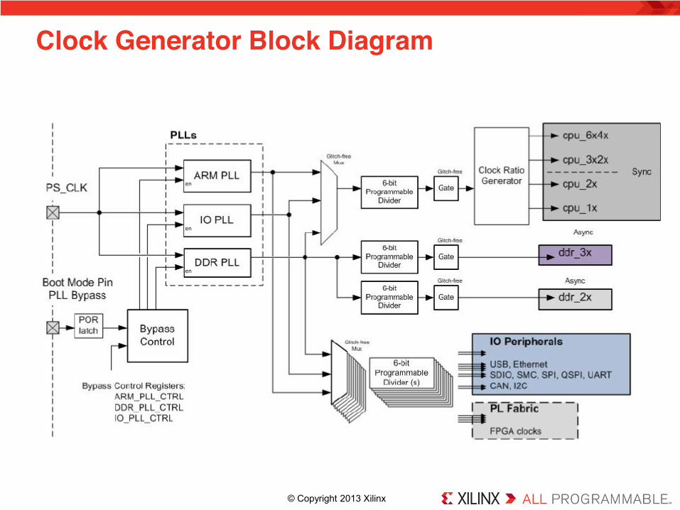
Clock Generator Block Diagram 1
- 2 0
© Copyright 2013 Xilinx .
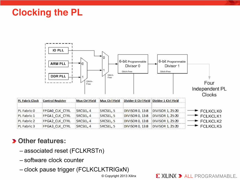
Clocking the PL
1
- 2 3
Other features: – associated reset (FCLKRSTn) – software clock counter – clock pause trigger (FCLKCLKTRIGxN)

© Copyright 2013 Xilinx .
16 peripheral interrupts from PL to PS –Used for accelerators and peripherals in PL
4 processor-specific interrupts from PL to PS 28 interrupts from PS peripherals to PL – PS peripherals can be serviced from Microblaze in fabric
Page 22
Interrupts

© Copyright 2013 Xilinx .
Interface Features SimilarTo MemoryMap/Full Traditional address/data burst
(single address,multiple data) PLBv46,PCI
Streaming Dataonly,burst LocalLink/DSP interfaces/FIFO/FSL
Lite Traditional address/data—no burst (single address,multiple data)
PLBv46single OPB
1
- 5
AXI is Part of AMBA: Advanced Microcontroller Bus Architecture

© Copyright 2013 Xilinx .
AXI Interface: Streaming
1
- 1 8
AXI Streams are fully handshaked –Data is transferred when source
asserts VALID and destination asserts READY
‘Information’ includes DATA and other side channel signals – STRB – KEEP – LAST – ID –DEST –USER
Most of these are optional
Inserting Wait States
Always Ready
Same Cycle Acknowledge

© Copyright 2013 Xilinx .
AXI Interface: AXI4
AXI4 READ AXI4 Write
1
- 2 4
Memory mapped interfaces consist of 5 streams – Read Address – Read Data – Write Address – Write Data – Write Acknowledge
Burst length limited to 256 Data width limited to 256 bits for Xilinx IP AXI Lite is a subset – no bursts – 32 bit data width only

© Copyright 2013 Xilinx .
AXI Interconnect IP in PS
Uses AXI4 Memory Mapped Interfaces – Automatic width conversion – Automatic AXI3/AXI4 Lite
protocol conversion – Automatic clock-domain
crossing
Configurable sparse crossbar or shared bus Optional buffering fifos Optional timing isolation registers
Page 26

© Copyright 2013 Xilinx .
Centralized arbitration with parallel data – Arbitration optimized for 3+ data beats per burst
Buffering allows address pipelining –However, Masters and Slaves have practical limits on pipelining –Described using Master ISSUING and Slave ACCEPTANCE parameters – Arbitration uses these parameters to limit head-of-line blocking
Page 27
AXI Interconnect IP Details

© Copyright 2013 Xilinx .
RA
DD
R
RD
ATA
WA
DD
R
WD
ATA
WR
ESP
Page 28
AXI based accelerators
HLS accelerators will combine lots of AXI interfaces
AXI4 Master
AXI4 Lite Slave
RA
DD
R
RD
ATA
WA
DD
R
WD
ATA
WR
ESP
AXI4 Stream AXI4 Stream

© Copyright 2013 Xilinx .
HP – 4 x 64 bit Slave interfaces • Optimized for high bandwidth
access from PL to external memory
GP – 2 x 32 bit Slave interfaces • Optimized for access from PL to
PS peripherals
– 2 x 32 bit Master interfaces • Optimized for access from
processors to PL registers
ACP – 1 x 64 bit Slave interface • Optimized for access from PL to
processor caches
Zynq AXI Interfaces
GP
ACP
HP

© Copyright 2013 Xilinx .
GP ports are designed for maximum flexibility Allow register access from PS to PL or PL to PS Good for Synchronization Prefer ACP or HP port for data transport
Page 30
GP Port Summary

© Copyright 2013 Xilinx .
HP ports are designed for maximum bandwidth access to external memory and OCM When combined can saturate external memory and OCM bandwidth –HP Ports : 4 * 64 bits * 150 MHz * 2 = 9.6 GByte/sec – external DDR: 1 * 32 bits * 1066 MHz * 2 = 4.3 GByte/sec –OCM : 64 bits * 222 MHz * 2 = 3.5 GByte/sec
Optimized for large burst lengths and many outstanding transactions Large data buffers to amortize access latency Efficient upsizing/downsizing for 32 bit accesses
Page 31
HP Port Summary

© Copyright 2013 Xilinx .
ACP allows limited support for Hardware Coherency – Allows a PL accelerator to access cache of the Cortex-A9 processors – PL has access to through the same path as CPUs • including caches, OCM, DDR, and peripherals
– Access is low latency (assuming data is in processor cache) • no switches in path
ACP does not allow full coherency – PL is not notified of changes in processor caches (different from ACE) – Use “event bus” or register write of PL register for synchronization
ACP is compromise between bandwidth and latency –Optimized for cache line length transfers – Low latency for L1/L2 hits –Minimal buffering to hide external memory latency –One shared 64 bit interface, limit of 8 masters
ACP Port Summary

© Copyright 2013 Xilinx .
Must access complete cache lines (32 bytes) – LENGTH = 3 (i.e. 4 data beats) – SIZE = 3 (i.e. transfer 8 bytes per data beat) – STRB = 0xFF (i.e. all data will be read/written) – Proper address alignment • Incremental burst with 32 byte alignment • Wrapped burst with 8 byte alignment
USER[0] = 1 and CACHE[0] = 1 to hit in cache
http://infocenter.arm.com/help/index.jsp?topic=/com.arm.doc.ddi0407f/BABCDDIA.html
Page 33
ACP Details

© Copyright 2013 Xilinx .
Programmable Logic
Common Peripherals
Zynq Processing
System
Memory Interfaces
ARM®
Dual Cortex-A9 MPCore™ System
Accelerator Architecture (With Bus Slave)
AXI4 interconnect
Pro: Simple System Architecture Con: Limited communication bandwidth
HDMI Output
Acc. 2 GP0 HP0
Acc. 1

© Copyright 2013 Xilinx .
Bus Slave Accelerator Communication
Write to Accelerator – processor writes to uncached
memory location
Read from Accelerator – processor reads from
uncached memory location
Page 35

© Copyright 2013 Xilinx .
Programmable Logic
Common Peripherals
Zynq Processing
System
Memory Interfaces
ARM®
Dual Cortex-A9 MPCore™ System
Architecture (With DMA)
AXI_DMA AXI_DMA
Pro: High Bandwidth Communication Con: Complicated System Architecture, High Latency
HDMI Output
GP0 HP0
HP1
Acc. 1 Acc. 2
AXI4 interconnect
AXI4 interconnect
© Copyright 2013 Xilinx .
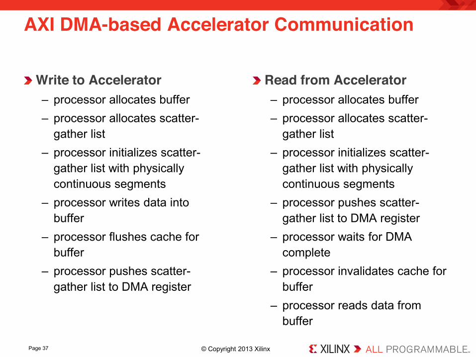
AXI DMA-based Accelerator Communication
Write to Accelerator – processor allocates buffer – processor allocates scatter-
gather list – processor initializes scatter-
gather list with physically continuous segments
– processor writes data into buffer
– processor flushes cache for buffer
– processor pushes scatter-gather list to DMA register
Read from Accelerator – processor allocates buffer – processor allocates scatter-
gather list – processor initializes scatter-
gather list with physically continuous segments
– processor pushes scatter-gather list to DMA register
– processor waits for DMA complete
– processor invalidates cache for buffer
– processor reads data from buffer
Page 37

© Copyright 2013 Xilinx .
Architecture (With Coherent DMA)
Pro: Low latency, high-bandwidth communication Con: Complicated system architecture, Limited to data that fits in caches
Programmable Logic
Common Peripherals
Zynq Processing
System
Memory Interfaces
ARM®
Dual Cortex-A9 MPCore™ System
AXI_DMA AXI_DMA
AXI4 interconnect HDMI Output
GP0 HP0
ACP
Acc. 1 Acc. 2
AXI4 interconnect
© Copyright 2013 Xilinx .
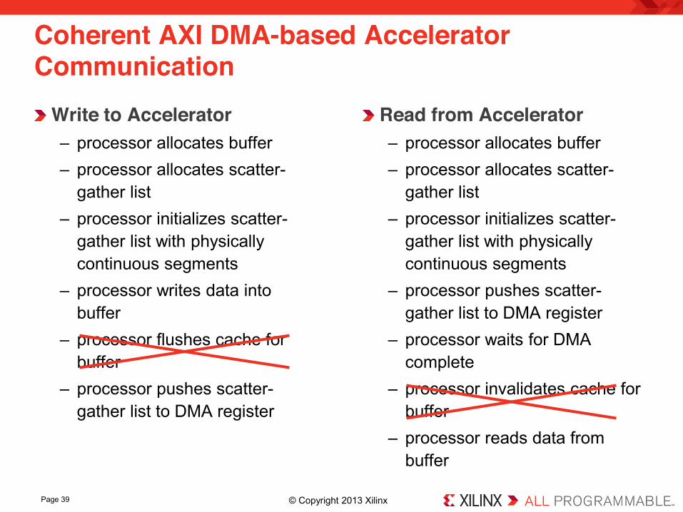
Coherent AXI DMA-based Accelerator Communication
Write to Accelerator – processor allocates buffer – processor allocates scatter-
gather list – processor initializes scatter-
gather list with physically continuous segments
– processor writes data into buffer
– processor flushes cache for buffer
– processor pushes scatter-gather list to DMA register
Read from Accelerator – processor allocates buffer – processor allocates scatter-
gather list – processor initializes scatter-
gather list with physically continuous segments
– processor pushes scatter-gather list to DMA register
– processor waits for DMA complete
– processor invalidates cache for buffer
– processor reads data from buffer
Page 39

© Copyright 2013 Xilinx .
How Does HLS Work?
Page 40

© Copyright 2013 Xilinx .
Overview of HLS HLS Coding and Design Capture Default Behaviors Performance Optimization Area Optimization Interface Definition
Page 41
How Does HLS Work?

© Copyright 2013 Xilinx .
Overview of HLS
Page 42

© Copyright 2013 Xilinx .
Page 43
HLS Premise: 1 C Code – Multiple HW Implementations

© Copyright 2013 Xilinx .
Functions – Functions define hierarchy and control regions
Function Parameters: –Define the RTL I/O Ports
Types: –Data types define bitwidth requirements –HLS optimizes bitwidth except for function
parameters
Loops: –Define iterative execution regions that can share HW
resources
Arrays: –Main way of defining memory and data storage
Operators: – Implementations optimized for performance – Automatically shared where possible to reduce area Page 44
Attributes of a Program for Synthesis

© Copyright 2013 Xilinx .
Page 45
Control Defined by a Program

© Copyright 2013 Xilinx .
Page 46
Combining Control and Operations

© Copyright 2013 Xilinx .
Page 47
Optimizing and Sizing Program Operations

© Copyright 2013 Xilinx .
Functions are by default converted into RTL modules Functions define hierarchy in RTL Functions at the same hierarchical level can be shared like any operator to reduce resource consumption – Performance requirements control the level possible sharing
Page 48
Program Functions and RTL Modules

© Copyright 2013 Xilinx .
Function parameters define data I/O ports and default protocols – Pointers → AXI4-Master interface – Scalars → AXI4-Lite interface or raw wires – Arrays → AXI4-Lite or AXI4 stream interface
Protocol in generated HW are controlled through user directives
Page 49
Completing a Design – I/O Port Creation

© Copyright 2013 Xilinx .
HLS Coding and Design Capture
Page 50

© Copyright 2013 Xilinx .
A complete C validation and verification environment – Vivado HLS supports complete bit-accurate validation of the C model – Vivado HLS provides a productive C-RTL co-simulation verification solution
Vivado HLS supports C, C++, and SystemC – Functions can be written in any version of C –Wide support for coding constructs in all three variants of C
Modeling with bit accuracy – Supports arbitrary precision types for all input languages – Allows the exact bit widths to be modeled and synthesized
Floating-point support – Support for the use of float and double in the code
Pointers and streaming-based applications
Page 51
Vivado HLS Development Environment

© Copyright 2013 Xilinx .
Two steps to verifying the design — Pre-synthesis: C validation
— Post-synthesis: RTL verification
C validation — Fast and free verification on any
Operating System
— Prove algorithm correctness before RTL generation
RTL Verification — RTL Co-Simulation against the
original program testbench
Page 52
Vivado HLS Tiered Verification Flow

© Copyright 2013 Xilinx .
Data Types – Forward declared data types –Recursive type definitions
Pointers –General casting between user defined data types – Pointers to dynamically allocated memory regions
System Calls –Dynamic memory allocation – must be replaced with static allocation – Standard I/O and file I/O – automatically ignored by the compiler – System calls • i.e. time(), sleep()
Recursive functions that are not compile time bounded STL lib calls –Not supported due to dynamic memory allocation –Have compile time unbounded recursion
Page 53
Coding Restrictions

© Copyright 2013 Xilinx .
C and C++ standard types are supported but limit the hardware – 8-bit, 16-bit, 32-bit boundaries
Real hardware implementations use a wide range of bitdwidths – Tailored to reduce hardware resources –Minimum precision to keep algorithm correctness
HLS provides bit-accurate types in C and C++ – SystemC and HLS types supported to simulate hardware datapaths in
C/C++
Page 54
Arbitrary Precision Types

© Copyright 2013 Xilinx .
Code using native C types Code using HLS types – Software model matches hardware implementation –C++ types can be compiled with both gcc and Visual Studio
Page 55
Algorithm Modeling with Arbitrary Types

© Copyright 2013 Xilinx .
Default Behavior
Page 56

© Copyright 2013 Xilinx .
HLS begins by extracting a functional model of a C expression
Page 57
Datapath Synthesis
+ * a
x
b + c
y
int a,b,c,x;
int y = a*x + b + c

© Copyright 2013 Xilinx .
HLS accounts for target frequency and device characteristics to determine minimum required pipelining Circuit will close timing but is not yet the optimal implementation
Page 58
Datapath Synthesis - Pipelining
a
y b
c
x
+ * +
int a,b,c,x;
int y = a*x + b + c

© Copyright 2013 Xilinx .
Automatic expression balancing for latency reduction Automatic restructuring to optimize use of FPGA fabric resources
Page 59
Datapath Synthesis - Optimization
b
y x
c
+ *
+
int a,b,c,x;
int y = a*x + b + c
a

© Copyright 2013 Xilinx .
Restructuring from previous stage leads to optimized implementations using DSP48
Page 60
Datapath Synthesis – Predictable Implementation
b
a
y x
c
+ *
+
DSP48
int a,b,c,x;
int y = a*x + b + c

© Copyright 2013 Xilinx .
After a datapath is generated, loop control logic is added
Page 61
Datapath and Loops
x y
control logic
start done
b
c
+ * +
int a,b,c,x,y;
for(int i = 0; i < 20; i++) {
x = get(); y = a*x + b + c; send(y);
}

© Copyright 2013 Xilinx .
C arrays can be implemented as BRAMs or LUT-RAMs Default implementation depends on the depth and bitsize of the original C array
Page 62
Defining Loop I/O with Arrays
in BRAM out
BRAM
i i
a x y
control logic
start done
b
c
+ * +
int a,b,c,x,y;
for(int i = 0; i < 20; i++) {
x = in[i]; y = a*x + b + c; out[i] = y;
}

© Copyright 2013 Xilinx .
Function parameters become system level interfaces after HLS synthesis
Page 63
Completing the Design – Interface Synthesis
in BRAM out
BRAM
i i
a x y
start done
b
c
AXI4-lite adapter logic
control logic
+ * +
f(int in[20], int out[20]) {
int a,b,c,x,y;
for(int i = 0; i < 20; i++) {
x = in[i]; y = a*x + b + c; out[i] = y;
}
}

© Copyright 2013 Xilinx .
Arrays and Pointers
Performance Optimization
Page 64

© Copyright 2013 Xilinx .
Arrays are the basic construct to express memory to HLS Default number of memory ports defined by –Number of usages in the algorithm – Target throughput
HLS default memory model assumes 2-port BRAMs Arrays can be reshaped and partitioned to remove bottlenecks –Changes to array layout do not require changes to the original code
Page 65
Arrays and Memory Bottlenecks

© Copyright 2013 Xilinx .
Examples: C array and RTL implementation
Page 66
Array Optimization - Dimensions

© Copyright 2013 Xilinx .
Partitioning splits arrays into independent memory banks in RTL Arrays can be partitioned on any dimension –Multi-dimension arrays can be partitioned multiple times –Dimension 0 applies a partitioning command to all dimensions
Page 67
Array Optimization - Partitioning
© Copyright 2013 Xilinx .
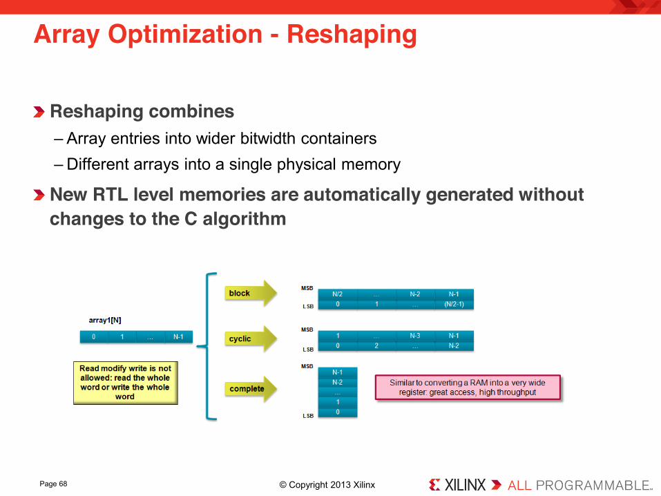
Reshaping combines – Array entries into wider bitwidth containers –Different arrays into a single physical memory
New RTL level memories are automatically generated without changes to the C algorithm
Page 68
Array Optimization - Reshaping

© Copyright 2013 Xilinx .
Structs can contain any mix of arrays and scalar values Structs are automatically partitioned into individual elements – Each struct variable becomes a separate port or data bus – Independent control logic for each struct member
Page 69
Array Optimization – Structs

© Copyright 2013 Xilinx .
Data packing creates a single wide bus for all struct members Bus Structure – First element in the struct becomes the LSB – Last element in the struct becomes the MSB – Arrays are partitioned completely
Page 70
Array Optimization – Structs and Data Packing

© Copyright 2013 Xilinx .
Example array initialization – Implies coeff is initialized at the start of each function call – Every function call has an overhead in writing the contents of the coeff
BRAM
Using static keyword moves initialization to bitstream – Values of coeff are part of the FPGA configuration bitstream –No function initialization overhead
Page 71
Array Optimization - Initialization

© Copyright 2013 Xilinx .
Standard mode – Each access results in a bus transaction –Read and write operations can be mapped into a single transaction
Burst mode –Uses the C memcpy method –Requires a local array inside the HLS block • Stores data for the burst write transaction • Stores data from the burs read transaction
Page 72
Pointer Optimization – Access Mode

© Copyright 2013 Xilinx .
Page 73
Pointer Optimization – Multiple Access

© Copyright 2013 Xilinx .
Loops
Performance Optimization
Page 74

© Copyright 2013 Xilinx .
Only perfect and semi-perfect loops are automatically optimized Perfect loops –Computation expressed only in the inner most loop –No initializations between loop statements – Loop bounds are constant
Semi-perfect loops –Computation expressed only in the inner most loop –No initializations between loop statements – Loop bounds can be variable
Other types of loops –User needs to convert the loop into
perfect or semi-perfect loop
Page 75
Loops - Classification

© Copyright 2013 Xilinx .
Each loop iteration runs in the same HW state Each loop iteration runs on the same HW resources
Page 76
Loop Default Behavior

© Copyright 2013 Xilinx .
Loops enforce a minimum execution latency Incrementing the loop counter always consumes 1 clock cycle Regardless of loop body, example will always take at least 4 clock cycles
Page 77
Loops and Latency

© Copyright 2013 Xilinx .
Page 78
Loops – Unrolling to Reduce Latency

© Copyright 2013 Xilinx .
HLS can unroll any loop by a factor Example shows unrolling by a factor of 2 – If N is not known, HLS inserts an exit
check to maintain algorithm correctness
– If N is known and fully divisible by the unrolling factor • Exit check is removed
Page 79
Loops – Partial Unrolling

© Copyright 2013 Xilinx .
Perfect and semi-perfect loops are automatically flattened – Flattening eliminates state transitions between loop hierarchy levels – A loop state transition (counter increment) takes 1 clock cycle
Automatic flattening can be turned off
Page 80
Loops - Flattening

© Copyright 2013 Xilinx .
Loop merging reduces control regions in the generated RTL Does not require code changes as long as – All loops have either constant or variable bounds but not both – Loop body code always generates the same result regardless of how many
times it is run • i.e A = B is always the same - A = A + 1 depends on the loop iteration count
Page 81
Loops - Merging

© Copyright 2013 Xilinx .
Loop merging eliminates redundant computation –Reduces latency –Reduces resources
Code implemented in RTL by HLS after merging
Page 82
Loops – Merging Example

© Copyright 2013 Xilinx .
Loops - Pipelining
Loop iterations run sequentially Throughput = 3 clock cycles Latency – 3 cycles per iteration – 6 cycles for entire loop
Loop iterations run in parallel Throughput = 1 clock cycle Latency – 3 cycles per iteration – 4 cycles for entire loop
Page 83

© Copyright 2013 Xilinx .
The number of clock cycles between start of new loop body.
II=1: one loop body per clock cycle – a ‘fully pipelined’ datapath for the loop body
II=2: one loop body every 2 clock cycles – Allows for resource sharing of operators.
Page 84
Loops - Initiation Interval (II)

© Copyright 2013 Xilinx .
II is expressed by the PIPELINE directive –Default value for PIPELINE = 1
Can be applied to any level of a loop hierarchy – Forces unrolling of any loop below the location of PIPELINE directive – Increases parallelism and resources in a generated implementation – Should be applied at a level that matches the input data rate of the design
Page 85
Loops – Hierarchy and II

© Copyright 2013 Xilinx .
Loop feedback is expressed as a dependence between iteration j to iteration j+1 Type of dependence can limit pipelining If a dependence limits pipelining, HLS automatically relaxes the constraint User requested II = 1 HLS generates II = 2 design due to dependence
Page 86
Loops – II and Feedback

© Copyright 2013 Xilinx .
HLS can instantiate all required resources to satisfy an II target within the boundaries of a generated module External ports can cause resource contention and are not automatically replicated – This type of contention can only be resolved by the user
Memory m is a top level port –HLS assumes only 1 port is available to function foo –Multiple read operations push II from 1 to 2
Page 87
Loops – II and Resource Contention

© Copyright 2013 Xilinx .
HLS pipelines by default stall if the next input is not available – For a loop, the next iteration doesn’t start if the input data is not ready – Stall affects all iterations currently being processed
Default stall can be avoided with the flush option – Flushing the pipeline allows iterations to finish execution regardless of the
state of the next iteration
Page 88
Loops – Pipeline Behavior

© Copyright 2013 Xilinx .
Dataflow is the parallel execution of multiple loops within a function Loops to run in parallel communicate through arrays Arrays are changed to FIFOs to allow concurrent execution of Loop_1 and Loop_2
Page 89
Loops - Dataflow

© Copyright 2013 Xilinx .
Functions
Performance Optimization
Page 90

© Copyright 2013 Xilinx .
For designs with multiple functions Default scheduling Functions can also be dataflowed like in the case of loops
Page 91
Functions

© Copyright 2013 Xilinx .
Area Optimization
Page 92

© Copyright 2013 Xilinx .
Page 93
Functions and RTL Hierarchy

© Copyright 2013 Xilinx .
Page 94
Function Inlining

© Copyright 2013 Xilinx .
Page 95
Function Inlining and Allocation

© Copyright 2013 Xilinx .
Combine multiple C arrays into 1 deeper memory Default is to concatenate arrays one after the other –User can introduce an offset to account for a system address map if the
combined memories are top level ports
Page 96
Array Mapping - Horizontal

© Copyright 2013 Xilinx .
Combine multiple C arrays into 1 wider memory Arrays use the same ordering as structs for packing – First array represents the LSB bits of the wider memory
Page 97
Array Mapping - Vertical

© Copyright 2013 Xilinx .
Interface Definition
Page 98

© Copyright 2013 Xilinx .
Clock –One clock per C/C++ design –Multiple clocks possible for SystemC designs
Reset – Applies to FSM and variables initialized in the C
algorithm
Clock Enable –Optional port –One clock enable per design – Attached to all modules within an HLS generated
design
Page 99
Default Ports

© Copyright 2013 Xilinx .
Function parameters –Data ports for RTL I/O
Function return – 1 per HLS design – Valid at the end of the C function call
Pointers –Can be implemented as both input and output – Transformed into separate ports for each
direction
Page 100
Function Parameters

© Copyright 2013 Xilinx .
RAM ports –Default port for an array – Assumes only 1 port connected to the HLS block – Automatic generation of address and data ports
FIFO ports – Example of streaming I/O – Assumes array is accessed in sequential order
Page 101
Function Parameters - Arrays

© Copyright 2013 Xilinx .
By default all HLS generated designs have a master control interface ap_start – Starts the RTL module, same as starting a
function call in C
ap_idle –RTL module is idle
ap_done –RTL module completed a function call – The data in the ap_return port is valid
ap_ready (not shown) –Only generated for designs with top level function
pipelining – Allows a processor to launch a new function call Page 102
Block-Level Protocol

© Copyright 2013 Xilinx .
Port I/O protocol – Selected by the user to integrate the HLS
generated block into a larger design –Control the sequencing of data on a per
interface basis
Allows mapping to AXI and HLS provided protocols – Interface synthesis in C and C++ designs
User can define their own interface protocol – SystemC designs natively express all port
interfaces
Page 103
I/O Data Transfer Protocols

© Copyright 2013 Xilinx .
Page 104
Connecting to Standard Buses

© Copyright 2013 Xilinx .
Let’s try it out!
Page 105
16x16 Matrix Multiply

© Copyright 2013 Xilinx .
Pick good places to pipeline. –#pragma HLS pipeline
Partition memories if needed. –#pragma HLS ARRAY_PARTITION variable=? complete dim=?
Watch for recurrences –Might need to rewrite code or pick a different algorithm
Use reduced-bitwidth operations. –ap_int<>, ap_uint<>, ap_fixed<>
Page 106
Basic AutoESL training in one slide

© Copyright 2013 Xilinx .
Page 107
Basic Matrix Multiply
void mm(int in_a[A_ROWS][A_COLS], int in_b[A_COLS][B_COLS], int out_c[A_ROWS][B_COLS]) { // matrix multiplication of a A*B matrix a_row_loop: for (int i = 0; i < A_ROWS; i++) { b_col_loop: for (int j = 0; j < B_COLS; j++) { int sum_mult = 0; a_col_loop: for (int k = 0; k < A_COLS; k++) { sum_mult += in_a[i][k] * in_b[k][j]; } out_c[i][j] = sum_mult; } } }
DSP48s: 3 Latency: 25121 clocks

© Copyright 2013 Xilinx .
Page 108
Pipelined Matrix Multiply
void mm_pipelined(int in_a[A_ROWS][A_COLS], int in_b[A_COLS][B_COLS], int out_c[A_ROWS][B_COLS]) { int sum_mult; // matrix multiplication of a A*B matrix a_row_loop: for (int i = 0; i < A_ROWS; i++) { b_col_loop: for (int j = 0; j < B_COLS; j++) { sum_mult = 0; a_col_loop: for (int k = 0; k < A_COLS; k++) { #pragma HLS pipeline sum_mult += in_a[i][k] * in_b[k][j]; } out_c[i][j] = sum_mult; } } }
DSP48s: 3 Latency: 6154 clocks Loop II: 1

© Copyright 2013 Xilinx .
void mm_parallel_dot_product(int in_a[A_ROWS][A_COLS], int in_b[A_COLS][B_COLS], int out_c[A_ROWS][B_COLS]) { #pragma HLS ARRAY_PARTITION DIM=2 VARIABLE=in_a complete #pragma HLS ARRAY_PARTITION DIM=1 VARIABLE=in_b complete int sum_mult; // matrix multiplication of a A*B matrix a_row_loop: for (int i = 0; i < A_ROWS; i++) { b_col_loop: for (int j = 0; j < B_COLS; j++) { #pragma HLS pipeline sum_mult = 0; a_col_loop: for (int k = 0; k < A_COLS; k++) { sum_mult += in_a[i][k] * in_b[k][j]; } out_c[i][j] = sum_mult; } } }
Page 109
Parallel Dot-Product Matrix Multiply
DSP48s: 48 Latency: 263 clocks Loop II: 1

© Copyright 2013 Xilinx .
void mm_pipelined_float(float in_a[A_ROWS][A_COLS], float in_b[A_COLS][B_COLS], float out_c[A_ROWS][B_COLS]) { float sum_mult; // matrix multiplication of a A*B matrix a_row_loop: for (int i = 0; i < A_ROWS; i++) { b_col_loop: for (int j = 0; j < B_COLS; j++) { sum_mult = 0.0; a_col_loop: for (int k = 0; k < A_COLS; k++) { #pragma HLS pipeline sum_mult += in_a[i][k] * in_b[k][j]; } out_c[i][j] = sum_mult; } } }
Page 110
Pipelined Floating Point Matrix Multiply
DSP48s: 1 Latency: 18453 clocks Loop II: 4

© Copyright 2013 Xilinx .
void mm_pipelined_float_interchanged(float in_a[A_ROWS][A_COLS], float in_b[A_COLS][B_COLS], float out_c[A_ROWS][B_COLS]) { float sum_mult[B_COLS]; // matrix multiplication of a A*B matrix a_row_loop: for (int i = 0; i < A_ROWS; i++) { a_col_loop: for (int k = 0; k < A_COLS; k++) { b_col_loop: for (int j = 0; j < B_COLS; j++) { #pragma HLS pipeline float last = (k==0) ? 0.0 : sum_mult[j]; float result = last + in_a[i][k] * in_b[k][j]; sum_mult[j] = result; if(k == (A_COLS-1)) out_c[i][j] = result; } } } }
Page 111
Pipelined Floating Point Matrix Multiply
DSP48s: 1 BRAM: 1 Latency: 4105 clocks Loop II: 1

© Copyright 2013 Xilinx .
#include <ap_int.h> void mm_18_parallel_dot_product(ap_int<18> in_a[A_ROWS][A_COLS], ap_int<18> in_b[A_COLS][B_COLS], ap_int<18> out_c[A_ROWS][B_COLS]) { #pragma HLS ARRAY_PARTITION DIM=2 VARIABLE=in_a complete #pragma HLS ARRAY_PARTITION DIM=1 VARIABLE=in_b complete ap_int<18> sum_mult; // matrix multiplication of a A*B matrix a_row_loop: for (int i = 0; i < A_ROWS; i++) { b_col_loop: for (int j = 0; j < B_COLS; j++) { #pragma HLS pipeline sum_mult = 0; a_col_loop: for (int k = 0; k < A_COLS; k++) { sum_mult += in_a[i][k] * in_b[k][j]; } out_c[i][j] = sum_mult; } } }
Page 112
18-bit Parallel Dot-Product Matrix Multiply
DSP48s: 16 Latency: 260 clocks Loop II: 1

© Copyright 2013 Xilinx .
Zynq Accelerated Applications
Page 113

© Copyright 2013 Xilinx .
X-Ray Tomography Scanning
256 x 367
sinoSize = 256*sqrt(2)
256
256
sinoNum = angles =
256
Video

© Copyright 2013 Xilinx .
Backprojection Algorithm structure
256 x 367
256 x 184
D1.1 D1.1 D1.1 128x93
D1.1 D1.1 D1.1 128x93
D1.1 D1.1 D1.1 128x93
D1.1 D1.1 D1.1 128x93 Back propagation
(base case) Partitioning
(recursive case 1) Angular Downsampling
(recursive case 2)
256 x 184
256 x 184
256 x 184
D1.1 D1.1 D1.1 64x47
D1.1 D1.1 D1.1 64x47
D1.1 D1.1 D1.1 64x47
D1.1 D1.1 D1.1 64x47
D1.1 D1.1 D1.1 64x47
D1.1 D1.1 D1.1 64x47
D1.1 D1.1 D1.1 64x47
D1.1 D1.1 D1.1 64x47
D1.1 D1.1 D1.1 64x47
D1.1 D1.1 D1.1 64x47
D1.1 D1.1 D1.1 64x47
D1.1 D1.1 D1.1 64x47
D1.1 D1.1 D1.1 64x47
D1.1 D1.1 D1.1 64x47
D1.1 D1.1 D1.1 64x47
D1.1 D1.1 D1.1 64x47

© Copyright 2013 Xilinx .
Total dataset will not easily fit in blockram or cache – 256x367x32bit = 275 KByte –Recursive case 1 is 2x input size –Recursive case 2 is same as input size
Downsampling reduces overall operations – Each downsampling stage reduces operations by factor 2.
Partitioning and Downsampling improves memory locality –Output data sets are smaller
Partitioning and Downsampling partitions data sets –Output data sets can be processed in parallel
Application characteristics

© Copyright 2013 Xilinx .
Open Source Linux-based Application –Compiles directly on ARM/Zynq – Single-precision floating point
Lots of things that are not synthesizable –Memory allocation – File I/O –Recursion
Backprojection Application

© Copyright 2013 Xilinx .
}
Code Structure
bp(sino,size, tau,img) if(size < limit) { direct(sino, size, tau, img); // Base case } else foreach quadrant { newSino = allocSino(newSinoSize, newNumSino); if(condition) { // With downsampling newSinoForNextIter(newSino, sino, newSinoSize); } else { // No downsampling newSinoForNextIter2(newSino, sino, newSinoSize); } subImage = getTile(img, quadrant); bp(newSino, newSize, tau, subImage); // Recursion case freeSino(newSino); }

© Copyright 2013 Xilinx .
Pointers must point to statically allocated structures Pointers to pointers must be inlined
Code Structure: HLS limitations
typedef struct{ int size; myFloat **pixel; //[size][size] } image; typedef struct{ int num; // number of angles int size; // length of each filtered sinograms myFloat T; myFloat **sino; //[size][size]; myFloat *sine; //[size]; myFloat *cosine; //[size]; } sinograms;

© Copyright 2013 Xilinx .
Two functions with HLS-generated accelerators – ap_newSinoForNextIter • Decomposes a sinogram into smaller sinogram tiles, with angular downsampling
– ap_direct • Computes result for a tile of the output image from a sinogram tile.
Most code runs on ARM –Memory allocation – File I/O – Sinogram Decomposition without angular downsampling
Pipelined Coherent DMA –Use good tile processing order for data locality
Page 120
Acceleration Approach
© Copyright 2013 Xilinx .
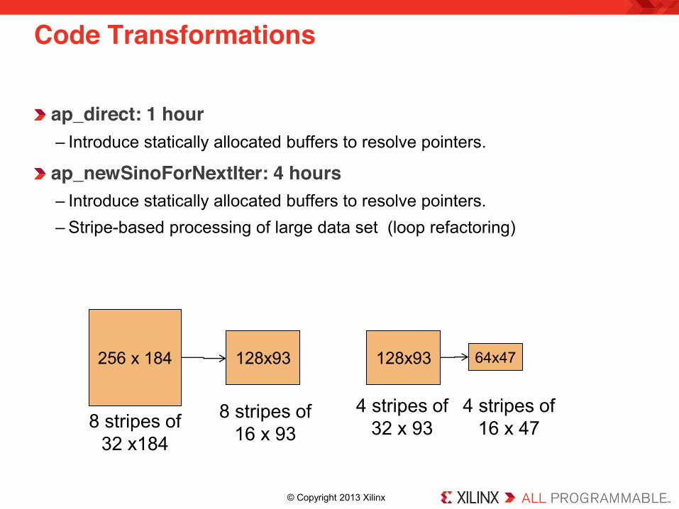
ap_direct: 1 hour – Introduce statically allocated buffers to resolve pointers.
ap_newSinoForNextIter: 4 hours – Introduce statically allocated buffers to resolve pointers. – Stripe-based processing of large data set (loop refactoring)
Code Transformations
256 x 184 128x93 64x47 128x93
8 stripes of 32 x184
4 stripes of 32 x 93
8 stripes of 16 x 93
4 stripes of 16 x 47

© Copyright 2013 Xilinx .
Architecture (With Coherent DMA)
Programmable Logic
Common Peripherals
Zynq Processing
System
Memory Interfaces
ARM®
Dual Cortex-A9 MPCore™ System
AXI_DMA AXI_DMA
AXI4 interconnect HDMI Output
GP0 HP0
ACP
Acc. 1 Acc. 2
AXI4 interconnect

© Copyright 2013 Xilinx .
Board + video
Page 123
Left side of the screen: SW running, ~ 1.5 fps
Right side of the screen: SW+ HW running, ~ 10 fps
HMDI Out
© Copyright 2013 Xilinx .
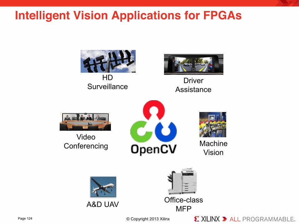
Intelligent Vision Applications for FPGAs
Machine Vision
Office-class MFP
Video Conferencing
Driver Assistance
HD Surveillance
A&D UAV
Page 124

© Copyright 2013 Xilinx .
Lane Detection – Algorithm Overview
Lane Detection – Analyze a video frame to detect road lane markings
Page 125
Lane Detection
RGB to Gray Conversion
Image Histogram
Equalization Edge
Detection Hough
Transform
Lane Detection

© Copyright 2013 Xilinx .
Total dataset will not easily fit in blockram or cache – 1920x1080x32 bit = ~8 MB
Predictable access patterns and algorithms with high spatial locality – line buffers and frame buffers
Applications are heterogeneous – Pixel processing (good for FPGA) – Frame-level processing (good for processor)
Application characteristics

© Copyright 2013 Xilinx .
Pixel processing accelerators with deep dataflow pipelines – Video Function library corresponding to OpenCV functions – Extract features from pixels
Frame rate processing runs on ARM –UI – Feature matching –Decision Making
Pipelined High performance DMA for video Features through general purpose interfaces
Page 127
Acceleration Approach

© Copyright 2013 Xilinx .
One image input, one image output – Processed by chain of functions sequentially
OpenCV Code
Image Read (OpenCV)
OpenCV function chain
Image Write (OpenCV)
… IplImage* src=cvLoadImage("test_1080p.bmp"); IplImage* dst=cvCreateImage(cvGetSize(src), src->depth, src->nChannels); cvSobel(src, dst, 1, 0); cvSubS(dst, cvScalar(100,100,100), src); cvScale(src, dst, 2, 0); cvErode(dst, src); cvDilate(src, dst); cvSaveImage("result_1080p.bmp", dst); cvReleaseImage(&src); cvReleaseImage(&dst); …
test_opencv.cpp
Page 128
© Copyright 2013 Xilinx .
Page 129
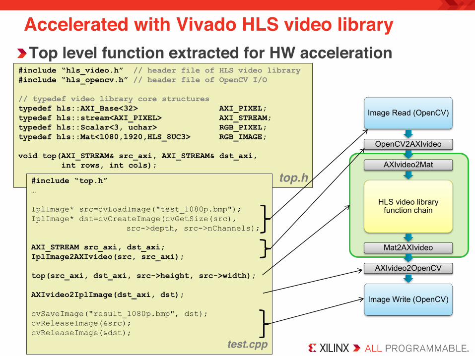
Accelerated with Vivado HLS video library Top level function extracted for HW acceleration
#include “hls_video.h” // header file of HLS video library #include “hls_opencv.h” // header file of OpenCV I/O // typedef video library core structures typedef hls::AXI_Base<32> AXI_PIXEL; typedef hls::stream<AXI_PIXEL> AXI_STREAM; typedef hls::Scalar<3, uchar> RGB_PIXEL; typedef hls::Mat<1080,1920,HLS_8UC3> RGB_IMAGE; void top(AXI_STREAM& src_axi, AXI_STREAM& dst_axi, int rows, int cols);
top.h
Image Read (OpenCV)
OpenCV2AXIvideo
AXIvideo2Mat
HLS video library function chain
Mat2AXIvideo
AXIvideo2OpenCV
Image Write (OpenCV)
#include “top.h” … IplImage* src=cvLoadImage("test_1080p.bmp"); IplImage* dst=cvCreateImage(cvGetSize(src), src->depth, src->nChannels); AXI_STREAM src_axi, dst_axi; IplImage2AXIvideo(src, src_axi); top(src_axi, dst_axi, src->height, src->width); AXIvideo2IplImage(dst_axi, dst); cvSaveImage("result_1080p.bmp", dst); cvReleaseImage(&src); cvReleaseImage(&dst);
test.cpp

© Copyright 2013 Xilinx .
#include “top.h” #include “ap_interfaces.h” void top(AXI_STREAM& src_axi, AXI_STREAM& dst_axi, int rows, int cols){ //Create AXI streaming interfaces for the core #pragma HLS RESOURCE core=AXIS variable=src_axi metadata="-bus_bundle INPUT_STREAM" #pragma HLS RESOURCE core=AXIS variable=dst_axi metadata="-bus_bundle OUTPUT_STREAM" #pragma HLS RESOURCE core=AXI_SLAVE variable=rows metadata="-bus_bundle CONTROL_BUS" #pragma HLS RESOURCE core=AXI_SLAVE variable=cols metadata="-bus_bundle CONTROL_BUS" #pragma HLS RESOURCE core=AXI_SLAVE variable=return metadata="-bus_bundle CONTROL_BUS" RGB_IMAGE img[6]; RGB_PIXEL pix(100,100,100); #pragma HLS dataflow hls::AXIvideo2Mat(src_axi, img[0]); hls::Sobel(img[0], img[1], 1, 0); hls::SubS(img[1], pix, img[2]); hls::Scale(img[2], img[3], 2, 0); hls::Erode(img[3], img[4]); hls::Dilate(img[4], img[5]); hls::Mat2AXIvideo(img[5], dst_axi); }
test.cpp
Accelerated with Vivado HLS video library
HW Synthesizable Block for FPGA acceleration – Consists of video library function and interfaces – Replace OpenCV function with similar function in hls namespace
Image Read (OpenCV)
OpenCV2AXIvideo
AXIvideo2Mat
HLS video library function chain
Mat2AXIvideo
AXIvideo2OpenCV
Image Write (OpenCV)
Page 130

© Copyright 2013 Xilinx .
2012.4 Beta: Video Library Function List
OpenCV I/O cvMat2hlsMat IplImage2hlsMat CvMat2hlsMat
OpenCV I/O hlsMat2cvMat hlsMat2IplImage hlsMat2CvMat
interfaces hls::AXIvideo2Mat interfaces hls::Mat2AXIvideo openCV basic function hls::Filter2D openCV basic function hls::Erode openCV basic function hls::Dilate openCV basic function hls::Min openCV basic function hls::Max openCV basic function hls::MinS openCV basic function hls::MaxS openCV basic function hls::Mul openCV basic function hls::Zero openCV basic function hls::Avg
openCV basic function hls::AbsDiff openCV basic function hls::CmpS openCV basic function hls::Cmp openCV basic function hls::And openCV basic function hls::Not openCV basic function hls::AddS openCV basic function hls::AddWeighted openCV basic function hls::Mean openCV basic function hls::SubRS openCV basic function hls::SubS openCV basic function hls::Sum openCV basic function hls::Reduce openCV basic function hls::Scale
For function signatures and descriptions, please refer to: – Synthesizable functions in hls_video.h – Interface functions in hls_opencv.h
Page 131

© Copyright 2013 Xilinx .
Page 132
Accelerator Architecture
Acc

© Copyright 2013 Xilinx .
Cost and power reduction by integrated solution Performance increase by exploiting the massive compute power of multi-core processors and programmable logic
LTE Radio Digital Front End: Digital Pre-Distortion
Page 133

© Copyright 2013 Xilinx .
Digital Pre-Distortion Functionality
Page 134
DPD negates PA non-linearity – PAs consume massive static power
– DPD improves PA efficiency by ~35-40%
Increase number of coefficients (K) – Better linearization, higher complexity
Estimate pre-distorter coefficients (A):
= Z A
x U(y)
(Nx1) (NxK)
(Kx1)
UHZ = UHUA W = VA
V-1W = A
LS Estimator
SW + Accelerators
HW
Coefficients (A)
VW
Alignment
Cholesky
PA Pre-Distorter
x z y0
y

© Copyright 2013 Xilinx .
Application characteristics
Page 135
Complex bare metal program – Multiple loop nests, with no
obvious bottleneck – Fixed and floating point – Complex numbers
Use software profiling – Focus on VW functionality
Initial Target: K = 64 – Look for speedup with minimal
hardware usage
More Speedup -> increase K
AlignmentVWCholesky
97%
3% 0%
x86 2GHz
Zynq 800MHz
Original 0.66s 1.20s
Target Update Time: 300ms (faster is better)

© Copyright 2013 Xilinx .
Code Structure
Page 136
for (int i = 0; i < NumCoeffs; ++i) { #pragma HLS pipeline II=2 W[i].real += (INT64)u[i].real*tx.real + (INT64)u[i].imag*tx.imag; W[i].imag += (INT64)u[i].real*tx.imag - (INT64)u[i].imag*tx.real; }
create_clock –period 5 set_part xc7z020clg484-2
Multipliers: 2 Adders: 2
© Copyright 2013 Xilinx .
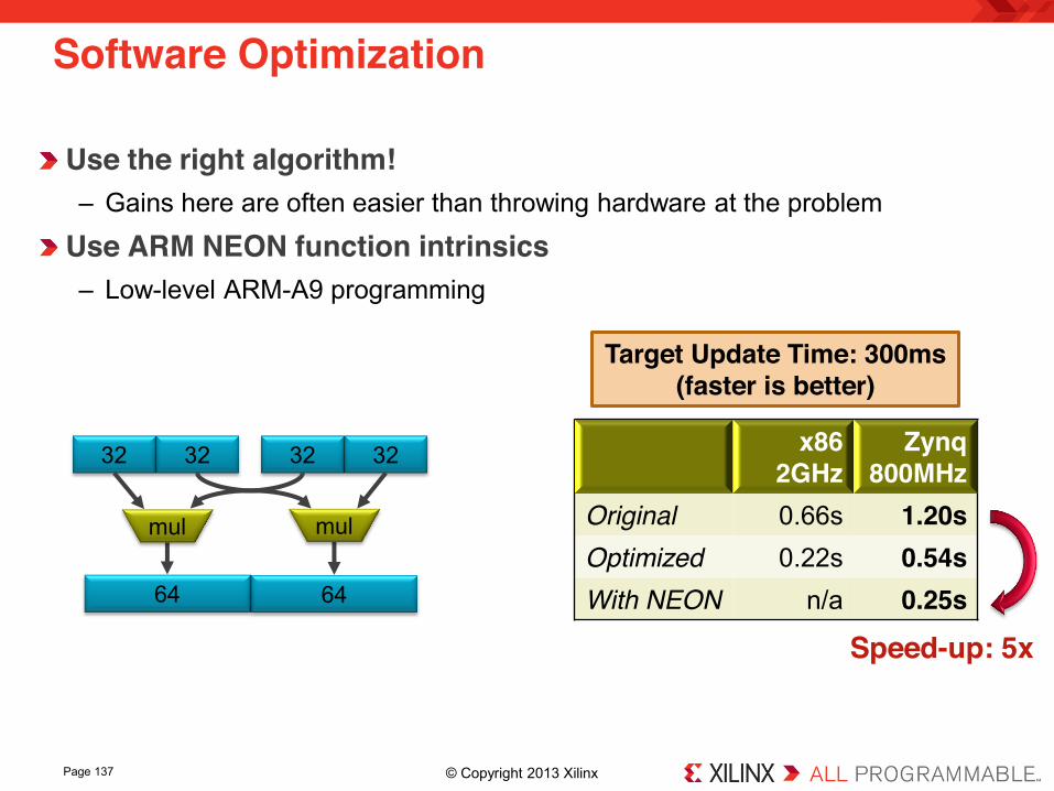
Software Optimization
Page 137
Use the right algorithm! – Gains here are often easier than throwing hardware at the problem
Use ARM NEON function intrinsics – Low-level ARM-A9 programming
x86 2GHz
Zynq 800MHz
Original 0.66s 1.20s Optimized 0.22s 0.54s With NEON n/a 0.25s
Target Update Time: 300ms (faster is better)
32 32 32 32
64 64
mul mul
Speed-up: 5x

© Copyright 2013 Xilinx .
Using NEON Instructions
Page 138
W[i].real += (INT64)uRow[i].real*sample.real + (INT64)uRow[i].imag*sample.imag;
// load operands int32x2_t tr = vdup_n_s32(sample.real); int32x2_t ti = vdup_n_s32(sample.imag); int32x2x2_t u = vld2_s32((int32_t *)(uRow+i)); int64x2_t w = vld1q_s64((int64_t *)(W+i)); // do parallel computation w = vmlal_s32(w,u.val[0],tr); w = vmlal_s32(w,u.val[1],ti); // store result vst1q_s64((int64_t *)(W+i),w);

© Copyright 2013 Xilinx .
Neon intrinsics are OK, but HLS can do better –with minimal code modification
Pick right partitioning between processor code and accelerator – Focus on efficient use of generated
hardware – Tradeoff overall time and resources • time = sw + communication + hw • resources = communication + hw
Efficient memory-mapped IO with fifo –DMA resources not justified
Page 139
Acceleration Approach
Run time
SW Comm.
HW
SW Comm.
HW
SW Comm.
HW

© Copyright 2013 Xilinx .
Programmable Logic
Common Peripherals
Zynq Processing
System
Memory Interfaces
ARM®
Dual Cortex-A9 MPCore™ System
AXI FIFO Architecture
VW Accelerator
GP0 AXI_FIFO
AXI4 interconnect
FF LUT
AXI Infrastructure ~300 ~300
Accelerator 2552 2605

© Copyright 2013 Xilinx .
0
250
500
750
1000
1250
Original Optimized NEON PL Accelerator
Cholesky
VW
Alignment
Digital Pre-Distortion on Zynq from C/C++
70x speed-up for VW
Page 141
Upd
ate
Tim
e (m
s)
3% ZC7020
Significant speed-up for existing designs OR: use speedup to solve bigger problems in same amount of time
© Copyright 2013 Xilinx .
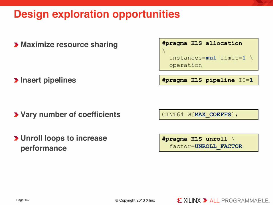
Design exploration opportunities
Maximize resource sharing Insert pipelines
Vary number of coefficients Unroll loops to increase performance
Page 142
#pragma HLS allocation \ instances=mul limit=1 \ operation
#pragma HLS pipeline II=1
#pragma HLS unroll \ factor=UNROLL_FACTOR
CINT64 W[MAX_COEFFS];

© Copyright 2013 Xilinx .
Accelerator Results
212
63 41 32 108 25 19 14
050
100150200250
NEON Unroll=1 Unroll=2 Unroll=4
Zynq
Not-OptimizedAlgorithmOptimizedalgorithm
(ms)
0 19 19 31 0 16 28 52 0
20
40
60
0
2000
4000
6000
NEON Unroll=1 Unroll=2 Unroll=4
Zynq Zynq
BRAMDSPFFLUT
Zynq & ARM
Zynq & ARM
VW Update Time
VW Accelerator Resources
64 Coefficients

© Copyright 2013 Xilinx .
Conclusion
Go forth and build!
Many thanks to: – Jan Langer – Baris Ozgul – Juanjo Noguera – Kees Vissers – Thomas Li – Devin Wang – Vinay Singh – Duncan Mackay – Dan Isaacs – And many others
Page 144