xcseries expansions with special functions
TRANSCRIPT

XC series expansions with special functions Operate Manual
Thinget Electronic Co., Ltd.

Catalog
Ⅰ 、 MODULE’S INFORMATION ....................................................................................................................... 3
Ⅱ 、 PID FUNCTION ............................................................................................................................................. 2
Ⅲ 、 ANALOG INPUT MODULE (XC-E8AD) .................................................................................................. 3
Ⅳ 、 ANALOG INPUT/OUTPUT MODULE XC-E4AD2DA ........................................................................ 12
Ⅴ 、 ANALOG OUTPUT MODULE XC-E4DA ............................................................................................... 19
Ⅵ 、 PT100 TEMPERATURE PID CONTROL MODULE XC-E6PT-P ...................................................... 24
Ⅶ 、 K TYPE THERMOCOUPLE TEMPERATURE PID CONTROL MODULE XC-E6TC-P ............ 30
VIII 、 XC-E3AD4PT2DA ................................................................................................................................. 36
ANALOG INPUT MODULE XC-E4AD .......................................................................................................... 46

Ⅰ、Module’s information
1、Basic Characteristic
XC series PLC have not only strong functions of logic dispose 、data operation、high speed disposing
etc. but also functions of A/D 、D/A convert、PID adjustment;With using expansions of analog input
module、analog output module、 temperature control module etc, XC series PLC are widely used in the
control system of temperature、flow、liquid level、pressure.
2、Module’s Name
The detailed information is the following:Model Function
XC-E8AD 8 channels analog input (14bit);4 channels current input, 4 channels voltage input XC-E4AD2DA 4 channels analog input (14bit); 2 channels analog output (12bit) ; current 、 voltage
selectable XC-E4DA 4 channels analog output (12bit);current、voltage selectableXC-E6PT-P -150 ~350℃ ℃,6 channels Pt100 temperature sampling, 0.1 degree precision, include PID
operationXC-E6TC-P 0 ~1000℃ ℃, 6 channels K type thermocouple temperature sampling module, 0.1 degree
precision, include PID operation
3、Exterior Size

4、General Specification
Operating Environment No Canker gas Ambient Temperature 0 ~60℃ ℃
Store Temperature -20~70℃Ambient Humidity 5~95%
Store Humidity 5~95%Installation Can be fixed with M3 screws or directly installed on orbit of
DIN46277(width: 35mm) Size 63mm×102mm×73.3mm
5、Items to note when using Please confirm the specification, choose suitable module
When carry on processing the screws or layout project, please protect the scraps falling into the modules
Before connecting, please confirm again module’s specification and connected device
When connecting, please check if the connection is fastness, cable breaking off will cause data incorrect,
short circuit and other fault! Installation, layout should only be carried after cutting all power.
Ⅱ、PID Function
1、Brief introduction of PID function
Among XC series PLC special modules, digital input module (A/D module) and temperature control
modules both have PID control function. It is widely used and flexible. When using, only four parameters
(Kp、 Ki、 Kd and Diff) should be set.
2、Parameter’s usage
Usage of four parameters: Proportion parameter(Kp)、Integral parameter(Ki)、Differential
parameter(Kd)、Control proportion band(Diff)Kp—parameter P is proportion parameter, mainly reflect system’s wrap. When wrap occurs, carry on control to
decrease this wrap. Ki—parameter I is integral parameter, mainly used to eliminate whisht difference, improving system’s no
difference degree.
Kd-- parameter D is differential parameter, mainly used to control signal’s changing trend, decrease system’s
shake.
Diff—Control bound means in the assigned bound, carry on PID control, out the bound, do not carry on PID
control.
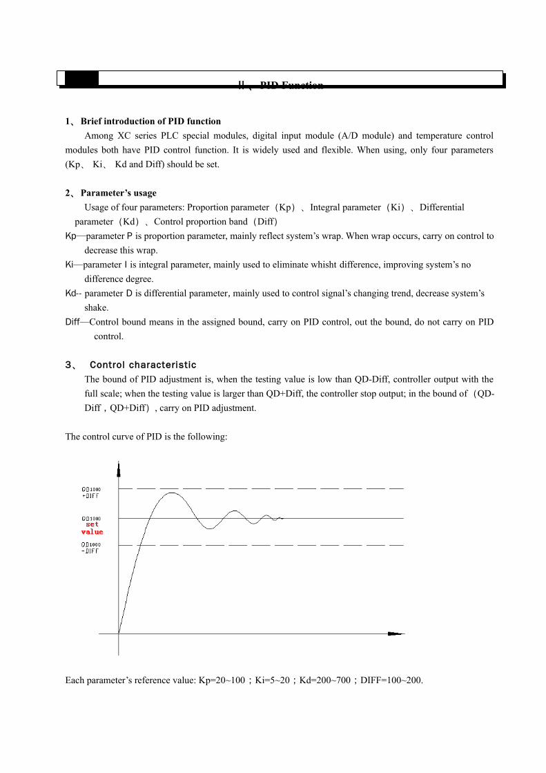
3、 Control characteristic The bound of PID adjustment is, when the testing value is low than QD-Diff, controller output with the
full scale; when the testing value is larger than QD+Diff, the controller stop output; in the bound of(QD-
Diff,QD+Diff), carry on PID adjustment.
The control curve of PID is the following:
Each parameter’s reference value: Kp=20~100;Ki=5~20;Kd=200~700;DIFF=100~200.

Ⅲ、Analog input module (XC-E8AD)
1.Specification
Specialty: 14 bits high precision analog input
8 channels analog input : The first
four channels current input
(0~20mA 、 4~20 mA two kinds) ;The left 4 channels voltage input
(0~5V、0~10V two kinds)
As special function module of XC, 7
models could be connected at most.
With PID adjustment function
Items Current input(0CH~3CH) Voltage input(4CH~7CH)Analog input bound DC0~20mA、4~20mA DC0~5V、0~10V
Max input bound 0~40mA ±18V
Digital output bound 14 bits binary data PID control value 0~4095Distinguish Ratio 1/16383(14Bit)
Integrate Precision 0.8%Convert speed 15ms per channel
Power used by analog DC24V±10%,100mAInstall format Can be fixed with M3 screws or directly installed on orbit of DIN46277 (width:
35mm)Size 63mm×102mm×73.3mm

2.Input ID assignment
XC series analog module doesn’t engross I/O units, the converted data is directly transferred into PLC
register. Channels’ correspond PLC register ID is:
Input、output ID list
Register’s ID of expansion 1:
Channel AD signal PID output value
PID start/stop control bit
The set value PID Parameters: Kp, Ki, Kd, control bound Diff, dead bound “Death”
0CH ID100 ID108 Y100 QD100 Kp:QD108
Ki:QD109
Kd:QD110
Diff:QD111
Death:QD112
1CH ID101 ID109 Y101 QD1012CH ID102 ID110 Y102 QD1023CH ID103 ID111 Y103 QD1034CH ID104 ID112 Y104 QD1045CH ID105 ID113 Y105 QD105
6CH ID106 ID114 Y106 QD1067CH ID107 ID115 Y107 QD107
Register’s ID of expansion 2:
Channel AD signal PID output value
PID start/stop control bit
The set value PID parameters:Kp, Ki, Kd, control bound Diff, dead bound “Death”
0CH ID200 ID208 Y200 QD200 Kp:QD208
Ki:QD209
Kd:QD210
Diff:QD211
Death:QD212
1CH ID201 ID209 Y201 QD2012CH ID202 ID210 Y202 QD2023CH ID203 ID211 Y203 QD2034CH ID204 ID212 Y204 QD2045CH ID205 ID213 Y205 QD205
6CH ID206 ID214 Y206 QD2067CH ID207 ID215 Y207 QD207
Register’s ID of expansion 3:
Channel AD signal PID output value
PID start/stop control bit
The set value PID parameters:Kp, Ki, Kd, control bound Diff, dead bound “Death”
0CH ID300 ID308 Y300 QD300 Kp:QD308
Ki:QD309
Kd:QD310
Diff:QD311
Death:QD312
1CH ID301 ID309 Y301 QD3012CH ID302 ID310 Y302 QD3023CH ID303 ID311 Y303 QD3034CH ID304 ID312 Y304 QD3045CH ID305 ID313 Y305 QD305
6CH ID306 ID314 Y306 QD3067CH ID307 ID315 Y307 QD307
Register’s ID of expansion 4:

Channel AD signal PID output value
PID start/stop control bit
The set value PID parameters:Kp, Ki, Kd, control bound Diff, dead bound “Death”
0CH ID400 ID408 Y400 QD400 Kp:QD408
Ki:QD409
Kd:QD410
Diff:QD411
Death:QD412
1CH ID401 ID409 Y401 QD4012CH ID402 ID410 Y402 QD4023CH ID403 ID411 Y403 QD4034CH ID404 ID412 Y404 QD4045CH ID405 ID413 Y405 QD405
6CH ID406 ID414 Y406 QD4067CH ID407 ID415 Y407 QD407
Register’s ID of expansion 5:
Channel AD signal PID output value
PID start/stop control bit
The set value PID parameters:Kp, Ki, Kd, control bound Diff, dead bound “Death”
0CH ID500 ID508 Y500 QD500 Kp:QD508
Ki:QD509
Kd:QD510
Diff:QD511
Death:QD512
1CH ID501 ID509 Y501 QD5012CH ID502 ID510 Y502 QD5023CH ID503 ID511 Y503 QD5034CH ID504 ID512 Y504 QD5045CH ID505 ID513 Y505 QD505
6CH ID506 ID514 Y506 QD5067CH ID507 ID515 Y507 QD507
Register’s ID of expansion 6:
Channel AD signal PID output value
PID start/stop control bit
The set value PID parameters :Kp、Ki、Kd、control bound Diff 、 dead bound “Death”
0CH ID600 ID608 Y600 QD600 Kp:QD608
Ki:QD609
Kd:QD510
Diff:QD611
Death:QD512
1CH ID601 ID609 Y601 QD6012CH ID602 ID610 Y602 QD6023CH ID603 ID611 Y603 QD6034CH ID604 ID612 Y604 QD6045CH ID605 ID613 Y605 QD605
6CH ID606 ID614 Y606 QD6067CH ID607 ID615 Y607 QD607
Register’s ID of expansion 7:
Channel AD signal PID output value
PID start/stop control bit
The set value PID parameters:Kp, Ki, Kd, control bound Diff, dead bound “Death”
0CH ID700 ID708 Y700 QD700 Kp:QD708
Ki:QD709
Kd:QD710
1CH ID701 ID709 Y701 QD7012CH ID702 ID710 Y702 QD7023CH ID703 ID711 Y703 QD7034CH ID704 ID712 Y704 QD704

Diff:QD711
Death:QD712
5CH ID705 ID713 Y705 QD705
6CH ID706 ID714 Y706 QD7067CH ID707 ID715 Y707 QD707
Description:Start signal(Y):when Y is 0, close PID control, when be 1 , start PID control
Parameter P:Proportion parameter, mainly reflex system’s difference, carry on control as soon as
difference occurs to improve the system’s no difference degree.
Parameter I:Integral parameter. Mainly used to remove whisht, improve the system’s no difference
degree. Parameter D:Differential parameter, mainly used to control signal’s changing trend,minish system’s
shake. Control bound Diff:In the assigned bound, carry on PID control. Beyond the bound, no PID control.
Dead area Death:When the current PID control value compares with the preceding PID control value. If
the difference between them is less than the set dead bound’s value, the module will
abnegate the current PID control value, send the preceding PID control value to the
PLC main unit.
Each parameter’s reference value:Kp=20~100;Ki=5~20;Kd=200~700;DIFF=100~200
3.Setting of working mode
1)Expansion’s 0CH~3CH channels have two modes to select: current 0~20mA、4~20mA , 4CH~7CH
channels have two modes to select, voltage 0~5V 、0~10V. Set via special FLASH data register FC inside
PLC. See the following table:
Module Channel’s ID 0CH~3CH 4CH~7CH
1# module FD8250 FD82512# module FD8258 FD82593# module FD8266 FD82674# module FD8274 FD82755# module FD8282 FD82836# module FD8290 FD82917# module FD8298 FD8299
Note:As showed in the preceding table, each register set 4 channels’ mode, each register has 16 bits. From
low bit to high bit, every 4 bits separately set 4 channels’ mode.
Each bit’s definition is showed in the following table:
The following, we take module 1 as example to describe the setting format:
Register FD8250:
Take 1# module as example:FD8250 H O O O O
0CH1CH2CH3CH
FD8251 H O O O O4CH5CH6CH7CH

Register FD8251:
E.g. : 1 ) Set module 1’s No. 3 、 No.2 、 No.1 、 No.0 channel’s working mode separately as
0~20mA、4~20mA、0~20mA、4~20mA, filters are all 1/2 filter, data in FD8250 is 0101H
2 ) Set module 1’s No. 7 、 No.6 、 No.5 、 No.4 channel’s working mode separately as
0~10V、0~5V、0~10V、0~5V, all the four channels don’t filter, data in FD8251 is 4545H
4.Exterior connection
About exterior connection, you should note the following two items:
When connect+24V power outside, please use the 24V power on PLC main unit to avoid interfere.
To avoid interfere, please use the shield cable and single point grounding with the shield layer.
Layout chart:
Channel 1 Channel 0Bit7 Bit6 Bit5 Bit4 Bit3 Bit2 Bit1 Bit0
00: 1/2 filter01: not filter10: 1/3 filter 11: 1/4 filter
- 0:0~20mA1:4~20mA
00: 1/2 filter01: not filter 10: 1/3 filter11: 1/4 filter
- 0:0~20mA1:4~20mA
- -
Channel 3 Channel 2
Bit15 Bit14 Bit13 Bit12 Bit11 Bit10 Bit9 Bit8
00: 1/2 filter 01: not filter 10: 1/3 filter 11: 1/4 filter
- 0:0~20mA1:4~20mA
00: 1/2 filter01: not filter10: 1/3 filter11: 1/4 filter
- 0:0~20mA1:4~20mA
- -
Channel 5 Channel 4Bit7 Bit6 Bit5 Bit4 Bit3 Bit2 Bit1 Bit0
00: 1/2 filter01: not filter10: 1/3 filter11: 1/4 filter
- 0:0~10V1:0~5V
00: 1/2 filter 01: not filter 10: 1/3 filter 11: 1/4 filter
- 0:0~10V1:0~5V
- -
Channel 7 Channel 6
Bit15 Bit14 Bit13 Bit12 Bit11 Bit10 Bit9 Bit8
00: 1/2 filter01: not filter 10: 1/3 filter11: 1/4 filter
- 0:0~10V1:0~5V
00: 1/2 filter01: not filter10: 1/3 filter11: 1/4 filter
- 0:0~10V1:0~5V
- -

5.Analog/digital convert chart
The relationship between input analog and converted digital quantity is showed in the following chart:
Current mode of Channel 0~Channel 3:
0~20mA analog input 4~20mA analog input

Voltage mode of Channel 4~Channel 7:
0~5V analog input 0~10V analog input
6.Programming
E.g. 1)Real time read unit 1 XC-E8AD module’s 8 channels’ data

MOV ID100 D0
END
M8000
MOV ID101 D1
MOV ID102 D2
MOV ID103 D3
MOV ID104 D4
MOV ID105 D5
MOV ID106 D6
MOV ID107 D7
E.g.2)Application of PID control in AD modules
The following, we take channel 0 of XC-E8AD as the example:
Write channel 0’s data in to data register D0
Write channel 1’s data in to data register D1
Write channel 2’s data in to data register D2
Write channel 3’s data in to data register D3
Write channel 5’s data in to data register D5
Write channel 4’s data in to data register D4
Write channel 7’s data in to data register D7
Write channel 6’s data in to data register D6

MOV ID100 D10
MOV ID108 D1000
M8000
MOV K30 QD108
MOV K10 QD109
MOV K300 QD110
MOV K100 QD111
MOV K200 QD112
MOV QD100D4000
END
Y100M8000
Write channel 0’s data into data register D10
Channel 0’s set value is register D4000
Set proportion coefficient Kp as 30
Set proportion coefficient Ki as 10
Set proportion coefficient Kd as 300
Set adjustment bound Diff as 100
Set control dead area as 200
Write channel 0’s PID value into register D1000
PID start/stop signal
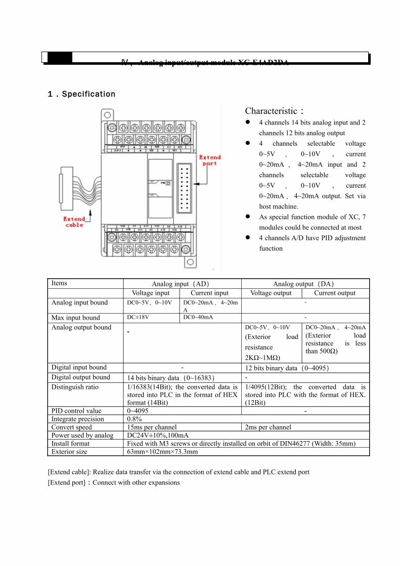
Ⅳ、Analog input/output module XC-E4AD2DA
1.Specification
Characteristic: 4 channels 14 bits analog input and 2
channels 12 bits analog output
4 channels selectable voltage
0~5V 、 0~10V , current
0~20mA 、 4~20mA input and 2
channels selectable voltage
0~5V 、 0~10V , current
0~20mA 、 4~20mA output. Set via
host machine.
As special function module of XC, 7
modules could be connected at most
4 channels A/D have PID adjustment
function
Items Analog input(AD) Analog output(DA)Voltage input Current input Voltage output Current output
Analog input bound DC0~5V、0~10V DC0~20mA 、4~20mA
-
Max input bound DC±18V DC0~40mA -
Analog output bound -
DC0~5V、0~10V
(Exterior load
resistance
2KΩ~1MΩ)
DC0~20mA 、 4~20mA (Exterior load resistance is less than 500Ω)
Digital input bound - 12 bits binary data(0~4095)Digital output bound 14 bits binary data(0~16383) -
Distinguish ratio 1/16383(14Bit); the converted data is stored into PLC in the format of HEX format (14Bit)
1/4095(12Bit); the converted data is stored into PLC with the format of HEX. (12Bit)
PID control value 0~4095 -Integrate precision 0.8%Convert speed 15ms per channel 2ms per channel Power used by analog DC24V±10%,100mAInstall format Fixed with M3 screws or directly installed on orbit of DIN46277 (Width: 35mm) Exterior size 63mm×102mm×73.3mm
[Extend cable]: Realize data transfer via the connection of extend cable and PLC extend port
[Extend port]:Connect with other expansions

2.The assignment of input/output ID
XC series analog modules do not engross I/O units, the converted data is directly transferred into PLC
register, analog output is also directly offered by PLC register.
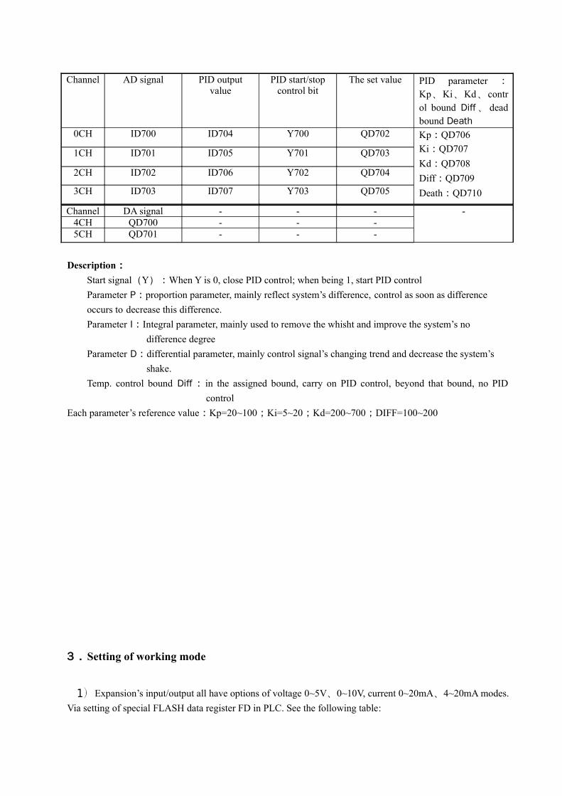
Register’s ID of expansion 1:
Channel AD signal PID output value
PID start/stop control bit
The set value PID parameter : Kp, Ki, Kd, control bound Diff, dead bound Death
0CH ID100 ID104 Y100 QD102 Kp:QD106
Ki:QD107
Kd:QD108
Diff:QD109
Death:QD110
1CH ID101 ID105 Y101 QD103
2CH ID102 ID106 Y102 QD104
3CH ID103 ID107 Y103 QD105
Channel DA signal - - - -4CH QD100 - - -5CH QD101 - - -
Register’s ID of expansion 2:
Channel AD PID output value
PID start/stop control bit
The set value PID parameter : Kp, Ki, Kd, control bound Diff, dead bound Death
0CH ID200 ID204 Y200 QD202 Kp:QD206
Ki:QD207
Kd:QD208
Diff:QD209
Death:QD210
1CH ID201 ID205 Y201 QD203
2CH ID202 ID206 Y202 QD204
3CH ID203 ID207 Y203 QD205
Channel DA signal - - - -4CH QD200 - - -5CH QD201 - - -
Register’s ID of expansion 3:Channel AD signal PID output
valuePID start/stop
control bitThe set value PID parameter : Kp,
Ki, Kd, control bound Diff, dead bound Death
0CH ID300 ID304 Y300 QD302 Kp:QD306
Ki:QD307
Kd:QD308
Diff:QD309
Death:QD310
1CH ID301 ID305 Y301 QD303
2CH ID302 ID306 Y302 QD304
3CH ID303 ID307 Y303 QD305
Channel DA signal - - - -4CH QD300 - - -5CH QD301 - - -

Register’s ID of expansion 4:Channel AD signal PID output
valuePID start/stop
control bitThe set value PID parameter : Kp,
Ki, Kd, control bound Diff, dead bound Death
0CH ID400 ID404 Y400 QD402 Kp:QD406
Ki:QD407
Kd:QD408
Diff:QD409
Death:QD410
1CH ID401 ID405 Y401 QD403
2CH ID402 ID406 Y402 QD404
3CH ID403 ID407 Y403 QD405
Channel DA signal - - - -4CH QD400 - - -5CH QD401 - - -
Register’s ID of expansion 5:Channel AD signal PID output
valuePID start/stop
control bitThe set value PID parameter :
Kp、Ki、Kd、control bound Diff 、 dead bound Death
0CH ID500 ID504 Y500 QD502 Kp:QD506
Ki:QD507
Kd:QD508
Diff:QD509
Death:QD510
1CH ID501 ID505 Y501 QD503
2CH ID502 ID506 Y502 QD504
3CH ID503 ID507 Y503 QD505
Channel DA signal - - - -4CH QD500 - - -5CH QD501 - - -
Register’s ID of expansion 6:Channel AD signal PID output
valuePID start/stop
control bitThe set value PID parameter :
Kp、Ki、Kd、control bound Diff 、 dead bound Death
0CH ID600 ID604 Y600 QD602 Kp:QD606
Ki:QD607
Kd:QD608
Diff:QD609
Death:QD610
1CH ID601 ID605 Y601 QD603
2CH ID602 ID606 Y602 QD604
3CH ID603 ID607 Y603 QD605
Channel DA signal - - - -4CH QD600 - - -5CH QD601 - - -
Register’s ID of expansion 7:
Channel AD signal PID output value
PID start/stop control bit
The set value PID parameter :Kp、Ki、Kd、control bound Diff 、 dead bound Death
0CH ID700 ID704 Y700 QD702 Kp:QD706
Ki:QD707
Kd:QD708
Diff:QD709
Death:QD710
1CH ID701 ID705 Y701 QD703
2CH ID702 ID706 Y702 QD704
3CH ID703 ID707 Y703 QD705
Channel DA signal - - - -4CH QD700 - - -5CH QD701 - - -
Description:Start signal(Y):When Y is 0, close PID control; when being 1, start PID control
Parameter P:proportion parameter, mainly reflect system’s difference, control as soon as difference
occurs to decrease this difference. Parameter I:Integral parameter, mainly used to remove the whisht and improve the system’s no
difference degree Parameter D:differential parameter, mainly control signal’s changing trend and decrease the system’s
shake. Temp. control bound Diff : in the assigned bound, carry on PID control, beyond that bound, no PID
control
Each parameter’s reference value:Kp=20~100;Ki=5~20;Kd=200~700;DIFF=100~200
3.Setting of working mode
1)Expansion’s input/output all have options of voltage 0~5V、0~10V, current 0~20mA、4~20mA modes.
Via setting of special FLASH data register FD in PLC. See the following table:

Module Channel’s ID0CH~3CH 4CH~5CH
1# expansion
FD8250 FD8251 low byte
2# expansion
FD8258 FD8259 low byte
3# expansion
FD8266 FD8267 low byte
4# expansion
FD8274 FD8275 low byte
5# expansion
FD8282 FD8283 low byte
6# expansion
FD8290 FD8291 low byte
7# expansion
FD8298 FD8299 low byte
Note:As shown in the preceding table, every register set 4 channels mode, each register has 16 bits, from low
to high, every 4 bits set separately 4 channels mode.
Each channel’s working mode is assigned by correspond register’s 4 bits. Each bit’s definition is showed in the
following table:
The following, we take module 1 as example to show how to set:
Register FD8250:
Register FD8251 low byte:
Channel 1 Channel 0Bit7 Bit6 Bit5 Bit4 Bit3 Bit2 Bit1 Bit0
00: 1/2 filter01: not filter10: 1/3 filter11: 1/4 filter
0: voltage input
0:0~10V1:0~5V
00: 1/2 filter01: not filter10: 1/3 filter11: 1/4 filter
0: voltage input
0:0~10V1:0~5V
1: current input
0:0~20mA1:4~20mA
1: current input
0:0~20mA1:4~20mA
Channel 3 Channel 2
Bit15 Bit14 Bit13 Bit12 Bit11 Bit10 Bit9 Bit8
00: 1/2 filter01: not filter10: 1/3 filter11: 1/4 filter
0: voltage input
0:0~10V1:0~5V
00: 1/2 filter01: not filter10: 1/3 filter11: 1/4 filter
0: voltage input
0:0~10V1:0~5V
1: current input
0:0~20mA1:4~20mA
1: current input
0:0~20mA1:4~20mA
Channel 5 Channel 4Bit7 Bit6 Bit5 Bit4 Bit3 Bit2 Bit1 Bit0
00: 1/2 filter01: not filter10: 1/3 filter11: 1/4 filter
0: voltage input
0:0~10V1:0~5V
00: 1/2 filter01: not filter10: 1/3 filter 11: 1/4 filter
0: voltage input
0:0~10V1:0~5V
1: current input
0:0~20mA1:4~20mA
1: current input
0:0~20mA1:4~20mA
Take 1# expansion as example :FD8250 H O O O O
0CH1CH2CH3CH
FD8251 H O O O O4CH5CH

E,g.: 1 ) If set working mode 0~20mA 、4~20mA 、0~10V、0~5V of module 1’s channel 3 、 channel
2、channel 1、channel 0, filters are all 1/2 filter, value in FD8250 is 2301H
4.Exterior connection
When carry on exterior connection, please note the following two items:
When connect+24V power outside, please choose 24V power on PLC main unit to avoid interfere.
To avoid interfere, please use shield cable and single point grounding with the shield layer.
Module’s 0~20mA or 4~20mA output need 24V power from outside, according to the analog output
register QD’s value, the module adjusts the loop circuit’s current, but the module itself doesn’t produce
current.
5.Analog digital convert chart
The relationship between input analog and converted digital is showed in the following chart:
0~5V analog input 0~10V analog input
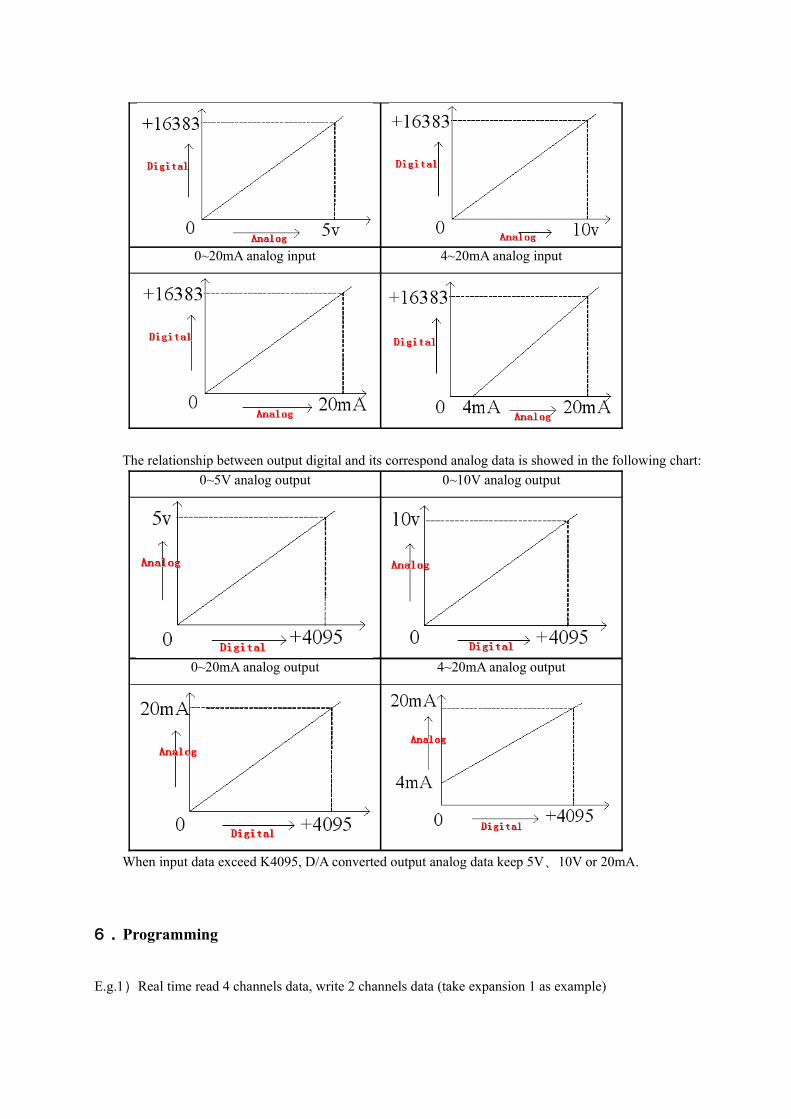
0~20mA analog input 4~20mA analog input
The relationship between output digital and its correspond analog data is showed in the following chart:
0~5V analog output 0~10V analog output
0~20mA analog output 4~20mA analog output
When input data exceed K4095, D/A converted output analog data keep 5V、10V or 20mA.
6.Programming
E.g.1)Real time read 4 channels data, write 2 channels data (take expansion 1 as example)

MOV ID100 D0
END
M8000
MOV ID101 D1
MOV ID102 D2
MOV ID103 D3
MOV D10 QD100
MOV D11 QD101
E.g.2)Applied method of PID (take expansion 1’s channel 0 as example)
MOV ID100 D10
MOV ID104 D1000
M8000
MOV K30 QD106
MOV K10 QD107
MOV K300 QD118
MOV K100 QD119
MOV K200 QD110
MOV QD100D4000
END
Y100M8000
Ⅴ、Analog output module XC-E4DA
Write channel 0’s data into data register D0
Write channel 1’s data into data register D1
Write channel 2’s data into data register D2
Write channel 3’s data into data register D3
Write data into data register D10 and give channel 4
Write data into data register D10 and give channel 5
Write channel 0’s data into data register D10
Channel 0’s set value is register D4000
Set proportion coefficient Kp as 30
Set proportion coefficient Ki as 10
Set proportion coefficient Kd as 300
Set adjustment bound Diff as 100
Set control dead area as 200
Write channel 0’s PID output value into register D1000
PID start signal

1、Specification
Characteristic: 12 bits high precision analog output
4 channels selectable voltage
0~5V 、 0~10V , current 0~20mA 、 4~20mA output
As special function module of XC, 7
modules could be connected
Items Voltage output Current outputAnalog output bound DC0~5V、0~10V DC0~20mA、4~20mADigital output bound 12 bits binary data Distinguish Ratio 1/4096(12Bit); the converted data is stored into PLC with the format of HEX Integrate precision 0.8%Convert speed 2ms per channel Insulate format DC/DC convert, optical coupling insulation Power for analog using DC24V±10%,100mAInstall format Can be fixed with M3 screws or directly installed on orbit of DIN46277 (width:
35mm)Exterior size 63mm×102mm×73.3mm
[Extend cable]:Realize data transfer via connecting of extend cable and PLC extend port
[Extend port]:Connect with other expansions
2.Assignment of Output ID

XC series analog module does not engross I/O units, the converted data is directly transferred into PLC
register. The output channel’s correspond PLC register ID is:
Output ID list
Channel No.1 unit No.2 unit No.3 unit No.4 unit No.5 unit No.6 unit No.7 unit0CH QD100 QD200 QD300 QD400 QD500 QD600 QD7001CH QD101 QD201 QD301 QD401 QD501 QD601 QD7012CH QD102 QD202 QD302 QD402 QD502 QD602 QD7023CH QD103 QD203 QD303 QD403 QD503 QD603 QD703
3.Setting of working mode
1 ) Each expansions’ input/output have the choice of voltage 0~5V 、 0~10V , current
0~20mA、4~20mA modes. Via the setting of special FLASH data register FD inside PLC, see the following
table:
Module Channel’s ID 0CH~3CH
1# module D8250 2# module D82583# module D82664# module D82745# module D82826# module D82907# module D8298
Each channel’s working mode is assigned by the correspond register’s 4 bits. Each bit’s definition is listed in
the following table:
Take module 1 as the example:
Register FD8250:
4.Exterior connection
Channel 1 Channel 0Bit7 Bit6 Bit5 Bit4 Bit3 Bit2 Bit1 Bit0
- 0:Voltage input
0:0~10V1:0~5V
- 0: Voltage input
0:0~10V1:0~5V
1:current input
0:0~20mA1:4~20mA
1:Current input
0:0~20mA1:4~20mA
Channel 3 Channel 2
Bit15 Bit14 Bit13 Bit12 Bit11 Bit10 Bit9 Bit8
- 0: Voltage input
0:0~10V1:0~5V
- 0: Voltage input
0:0~10V1:0~5V
1: current input
0:0~20mA1:4~20mA
1: current input
0:0~20mA1:4~20mA
Take expansion1 as the example:FD8250 H O O O O
0CH1CH2CH3CH

When carry on exterior connection, please note the following two items:
When connect+24V power outside, please choose 24V power on PLC main unit to avoid interfere.
To avoid interfere, please use shield cable and single point grounding with the shield layer.
Module’s 0~20mA or 4~20mA output need 24V power from outside, according to the analog output
register QD’s value, the module adjusts the loop circuit’s current, but the module itself doesn’t produce
current.

5.Analog digital convert chart
The relationship between PLC’s output digital and its correspond analog data is showed in the following
chart:
0~5V analog output 0~10V analog output
0~20mA analog output 4~20mA analog output
When the output data exceed K4095, D/A converted output analog data keep 5V、10V or 20mA
6.Programming
Real time write data into 4 channels
MOV D10 QD100
END
M8000
MOV D11 QD101
MOV D12 QD102
MOV D13 QD103
Write data into data register D10 and give channel 0
Write data into data register D11 and give channel 1
Write data into data register D13 and give channel 3
Write data into data register D12 and give channel 2

Ⅵ、Pt100 temperature PID control module XC-E6PT-P
1.Specification
Characteristic:
Platinum thermo-resistance input, Pt100
6 channels input, 6 channels output
2 groups PID parameters (every 3
channels has a group of PID parameter)
1mA lasting current output, not affected
by the exterior environment
Distinguish ratio is 0.1℃
As special function module of XC, 7
modules could be connected
Item ContentAnalog input signal Pt100 platinum thermo-resistance Temperature testing bound
-100 ~350℃ ℃
Digital output bound -1000~3500,16 bits with sign bit, binary Control precision ±0.5℃Distinguish ratio 0.1℃Integrate precision ±0.8%(relative to the max value)Convert speed 100ms×6 channelsAnalog using power DC24V±10%,50mAInstall format Fixed with M3 screws or directly installed on orbit of DIN46277 (Width: 35mm)Exterior size 63mm×102mm×73.3mm
[Extend cable]:Realize data transfer via the connection of extend cable and PLC extend port.
[Extend port]: Connect with other expansions
Note:1、Without signal input, the channel’s data is 3500
2、According to the actual requirement, connect with Pt100 platinum thermo-resistance

2.Assignment of input definition ID
XC series analog modules don’t engross I/O units, the converted data is directly transferred into PLC
register, channel’s correspond PLC register’s ID is:
Table of input definition ID:
Channel 1#module 2#module 3#module 4#module 5#module 6#module 7#module0CH ID100 ID200 ID300 ID400 ID500 ID600 ID7001CH ID101 ID201 ID301 ID401 ID501 ID601 ID7012CH ID102 ID202 ID302 ID402 ID502 ID602 ID7023CH ID103 ID203 ID303 ID403 ID503 ID603 ID7034CH ID104 ID204 ID304 ID404 ID504 ID604 ID7045CH ID105 ID205 ID305 ID405 ID505 ID605 ID705
Table of output definition ID:
Channel 1#module 2#module
3#module
4#module
5#module
6#module
7#module
0CH set temperature
QD100 QD200 QD300 QD400 QD500 QD600 QD700
1CH set temperature
QD101 QD201 QD301 QD401 QD501 QD601 QD701
2CH set temperature
QD102 QD202 QD302 QD402 QD502 QD602 QD702
3CH set temperature
QD103 QD203 QD303 QD403 QD503 QD603 QD703
4CH set temperature
QD104 QD204 QD304 QD404 QD504 QD604 QD704
5CH set temperature
QD105 QD205 QD305 QD405 QD505 QD605 QD705
First 3 channels P parameter
QD106 QD206 QD306 QD406 QD506 QD606 QD706
First 3 channels I parameter
QD107 QD207 QD307 QD407 QD507 QD607 QD707
First 3 channels D parameter
QD108 QD208 QD308 QD408 QD508 QD608 QD708
First 3 channels temperature control bound
QD109 QD209 QD309 QD409 QD509 QD609 QD709
Last 3 channels P parameter
QD110 QD210 QD310 QD410 QD510 QD610 QD710
Last 3 channels I parameter
QD111 QD211 QD311 QD411 QD511 QD611 QD711
Last 3 channels D parameter
QD112 QD212 QD312 QD412 QD512 QD612 QD712
Last 3 QD113 QD213 QD313 QD413 QD513 QD613 QD713

channels temperature control bound
Description:Start signal(Y):When Y is 0, close PID control; when being 1, start PID control
Parameter P:proportion parameter, mainly reflect system’s difference, control as soon as difference
occurs to decrease this difference. Parameter I:Integral parameter, mainly used to remove the whisht and improve the system’s no
difference degree Parameter D:differential parameter, mainly control signal’s changing trend and decrease the system’s
shake. Temp. control bound Diff : in the assigned bound, carry on PID control, beyond that bound, no PID
control
Each parameter’s reference value:Kp=20~100;Ki=5~20;Kd=200~700;DIFF=100~200
3.Setting of input filter
1)Every input of expansion has option of filter, set via special FLASH data register FD in PLC.
Seethe following chart:
Module channel’s ID0CH~3CH 4CH~5CH
1#module FD8250 FD8251low byte2# module FD8258 FD8259 low byte3# module FD8266 FD8267 low byte4# module FD8274 FD8275 low byte5# module FD8282 FD8283 low byte6# module FD8290 FD8291 low byte7# module FD8298 FD8299 low byte
Each channel’s filter mode is assigned via correspond register’s 4 bits! Each bit’s definition is showed in the
following table:
Take module 1 as the example:
Register FD8250:
Take 1# module as example:FD8250 H O O O O
0CH1CH2CH3CH
FD8251 H O O O O4CH5CH

Register FD8251:
When leave the factory, the defaulted value is 0, the initial filter format is 1/2 filter.
4.Exterior connection
About outside layout, you should note the following two items:
When carry on+24V power, please use 24V power on PLC main unit to avoid interfere.
To avoid interfere, please take shield measure with the signal cable.
Input connection:
Channel 2 Channel 1Bit7 Bit6 Bit5 Bit4 Bit3 Bit2 Bit1 Bit0
00:1/2 filter01:not filter10:1/3 filter11:1/4 filter
- - 00:1/2 filter01:not filter10:1/3 filter11:1/4 filter
- -
- - - -
Channel 4 Channel 3
Bit15 Bit14 Bit13 Bit12 Bit11 Bit10 Bit9 Bit8
00:1/2 filter01:not filter10:1/3 filter11:1/4 filter
- - 00:1/2 filter01:not filter10:1/3 filter11:1/4 filter
- -
- - - -
Channel 5 Channel 4Bit7 Bit6 Bit5 Bit4 Bit3 Bit2 Bit1 Bit0
00:1/4 filter01:不 filter 10:1/2 filter11:1/3 filter
- - 00:1/4 filter01:不 filter10:1/2 filter11:1/3 filter
- -
- - - -

A0C0 C1
A1C2
A2 A3C3
A4C4
A5C5
Y0COM0
Y2Y5COM2
Y1 Y4Y3COM1
Y
AI
PWR
543210
Output terminals
Transistor output terminals, please choose DC5V~30V flat power.
Circuit insulation
Between PLC’s interior circuit and output transistor, use optical insulation. Each public module is also
separate.
Response time
The time from PLC drive (or cut) optical coupling device to transistor ON/OFF, no more than 0.2ms.
Output current
Each point has electricity 0.8A, but to avoid temperature rising, please use as every 4 points 1.2A or
every 8 points 2.0A
Open circuit leak current
Below 0.1mA
The output circuit is the following:
Take channel 0 and channel 1 as the example:

6.Programming
Program with the first channel
K800MOV QD100
K500MOV QD108
K5MOV QD107
K30MOV QD106
M8000
FEND
K150MOV QD109
Y100M0
Set channel 0’s set value as 800 (80 degrees)
Set channel 0’s proportion coefficient Kp as 30
Start/stop channel 0
Set channel 0’s proportion coefficient Ki as 5
Set channel 0’s proportion coefficient Kd as 500
Set channel 0’s proportion band Diff as 150(enter PID operation at 650)

Ⅶ、K type thermocouple temperature PID control module XC-E6TC-P
1.Specification
Characteristic:
Thermocouple K type analog input used
by temperature sensor
6 channels input, 6 channels output
2 groups PID parameters (one group
PID parameters every 3 channels)
Hide cold-terminal compensate circuit
inside
Distinguish precision is 0.1℃
As special function module of XC , 7
modules could be connected at most
Items ContentAnalog input signal K type thermocouple Temperature testing bound 0 ~1000℃ ℃Digital output bound 0~10000,16 bits with sign bit, binary Control precision ±0.5℃Distinguish ratio 0.1℃Integrate precision ±0.8% (compare with the max value)Convert speed 100ms×6 channelsPower for analog using DC24V±10%,50mAInstall format Fixed with M3 screws or directly installed on orbit of DIN46277 (Width:
35mm)Exterior size 63mm×102mm×73.3mm
[Extend cable]:Realize data transfer via the connection of extend cable and PLC extend port
[Extend port]: Connect with other expansion
Note:1、If no signal input, the channel’s data is 0
2、According to the actual requirement, connect with K type thermocouple

2.Assignment of input ID
XC series analog modules don’t engross I/O units, the converted data is directly transferred into PLC
register, channel’s correspond PLC register’s ID is:
Input ID list
Channel 1# Expansion
2# Expansion
3# Expansion
4# Expansion
5# Expansion
6# Expansion
7# Expansion
0CH ID100 ID200 ID300 ID400 ID500 ID600 ID7001CH ID101 ID201 ID301 ID401 ID501 ID601 ID7012CH ID102 ID202 ID302 ID402 ID502 ID602 ID7023CH ID103 ID203 ID303 ID403 ID503 ID603 ID7034CH ID104 ID204 ID304 ID404 ID504 ID604 ID7045CH ID105 ID205 ID305 ID405 ID505 ID605 ID705
Output ID list
Channel’s ID and parameter
1# Expansion
2# Expansion
3# Expansion
4# Expansion
5# Expansion
6# Expansion
7# Expansion
0CH set temperature
QD100 QD200 QD300 QD400 QD500 QD600 QD700
1CH set temperature
QD101 QD201 QD301 QD401 QD501 QD601 QD701
2CH set temperature
QD102 QD202 QD302 QD402 QD502 QD602 QD702
3CH set temperature
QD103 QD203 QD303 QD403 QD503 QD603 QD703
4CH set temperature
QD104 QD204 QD304 QD404 QD504 QD604 QD704
5CH set temperature
QD105 QD205 QD305 QD405 QD505 QD605 QD705
First 3 channels P para.
QD106 QD206 QD306 QD406 QD506 QD606 QD706
First 3 channels I para.
QD107 QD207 QD307 QD407 QD507 QD607 QD707
First 3 channels D para.
QD108 QD208 QD308 QD408 QD508 QD608 QD708
First 3 channels temp. control bound
QD109 QD209 QD309 QD409 QD509 QD609 QD709
Last 3 channels P para.
QD110 QD210 QD310 QD410 QD510 QD610 QD710
Last 3 channels I para.
QD111 QD211 QD311 QD411 QD511 QD611 QD711
Last 3 channels D para.
QD112 QD212 QD312 QD412 QD512 QD612 QD712

Last 3 channels temp. control bound
QD113 QD213 QD313 QD413 QD513 QD613 QD713
Description:Start signal(Y):When Y is 0, close PID control; when being 1, start PID control
Parameter P:proportion parameter, mainly reflect system’s difference, control as soon as difference
occurs to decrease this difference. Parameter I:Integral parameter, mainly used to remove the whisht and improve the system’s no
difference degree Parameter D:differential parameter, mainly control signal’s changing trend and decrease the system’s
shake. Temp. control bound Diff : in the assigned bound, carry on PID control, beyond that bound, no PID
control
Each parameter’s reference value:Kp=20~100;Ki=5~20;Kd=200~700;DIFF=100~200
3.Input filter setting
Every input of expansions has filter option, set via special FLASH data register FD inside PLC. See the
following chart:
Module Channel’s ID 0CH~3CH 4CH~5CH
1# module FD8250 FD8251 Low byte 2# module FD8258 FD8259 Low byte3# module FD8266 FD8267 Low byte4# module FD8274 FD8275 Low byte5# module FD8282 FD8283 Low byte6# module FD8290 FD8291 Low byte7# module FD8298 FD8299 Low byte
Each channel’s filter mode is assigned by correspond register’s 4 bits. Each bit’s definition is showed in the
following table:
Take module 1 as example
Register FD8250:
Take 1# module as example :FD8250 H O O O O
0CH1CH2CH3CH
FD8251 H O O O O4CH5CH

Register FD8251:
When leave the factory, their defaulted value is 0, i.e. the initial filter format is 1/4 filter
4.Exterior connection
About the exterior connection, you should pay attention to the following two items:
When connect with+24V power outside, please use the 24V power on PLC main unit to avoid interfere
To avoid interfere, shield measure is necessary for the signal cables
Input method:
Channel 1 Channel 0Bit7 Bit6 Bit5 Bit4 Bit3 Bit2 Bit1 Bit0
00:1/4 filter01:not filter10:1/2 filter11:1/3 filter
- - 00:1/4 filter01:not filter10:1/2 filter11:1/3 filter
- -
- - - -
Channel 3 Channel 2
Bit15 Bit14 Bit13 Bit12 Bit11 Bit10 Bit9 Bit8
00:1/4 filter 01:not filter10:1/2 filter11:1/3 filter
- - 00:1/4 filter 01:not filter10:1/2 filter11:1/3 filter
- -
- - - -
Channel 5 Channel 4Bit7 Bit6 Bit5 Bit4 Bit3 Bit2 Bit1 Bit0
00:1/4 filter01:not filter10:1/2 filter11:1/3 filter
- - 00:1/4 filter01:not filter10:1/2 filter11:1/3 filter
- -
- - - -

0 1 2 34 5
PWR
AI
Y
TC5-TC5+
TC0-TC0+ TC2+
TC1- TC2- TC3- TC4-TC4+TC3+TC1+
COM1 Y3Y4Y1
COM2 Y5Y2
COM0Y0
Output terminal
For transistor output terminals, flat please use power of DC5V~30V.
Circuit insulation
Between PLC interior circuit and output transistor, carry on optical insulation with optical coupling
device. Each public modules are separate.
Response time
The time form PLC drive (or cut) optical coupling circuit to transistor’s ON/OFF, no more than 0.2ms
Output circuit
Each point’s current 0.8A. But to restrict the increase of temperature,, please use in the condition of
every 4 points 1.2A or every 8 points 2.0A
Open circuit leak current
Below 0.1mA.
The output circuit is the following:
Take channel 0 and channel 1 as the example:

6.Program
Program with the first channel
K800MOV QD100
K500MOV QD108
K5MOV QD107
K30MOV QD106
M8000
FEND
K150MOV QD109
Y100M0
Set channel 0’s value as 800 (80 degrees)
Set channel 0’s proportion coefficient Kp as 30
Start / stop channel 0
Set channel 0’s proportion coefficient Ki as 5
Set channel 0’s proportion coefficient Kd as 500
Set channel 0’s proportion band Diff as 150(At 650, carry on PID operation)

VIII、XC-E3AD4PT2DA
1.Specifications
Specilities: 3 channels 14 bits current input 、 4
channels PT100 temperature input and 2
channels 12 bits voltage output
3 channels current 0~20mA 、 4~20mA
input (selectable) and 2 channels voltage
0~5V、0~10V output (selectable), set via
the software
Pt resistor input (PT100)
3 channels A/D and 4 channels PT input,
with PID adjustment function
ITEMSAnalog Current Input
(AD)Temperature Input (PT) Analog Voltage Output
(DA)Analog Input DC0~20mA、4~20mA PT100 -
Temperature Testing Bound
- -100~350℃ -
Maximum Output Bound
DC0~40mA - -
Analog Output Bound - -
DC0~5V、0~10V
External load resistor
(2KΩ~1MΩ)Digital Input Bound
- - 12 bits binary (0~4095)
Digital Output Bound
14 bits binary (0~16383) -1000~3500 -
Distinguish 1/16383(14Bit); the converted data is stored into PLC(14Bit) in the form of Hex.
0.1℃ 1/4095(12Bit); the converted data is stored into PLC(12Bit) in the form of Hex.
PID Output Value 0~K4095 -General Precision
0.8% ±0.5℃ 0.8%
Convert Speed 20ms per channel 3ms per channelPower Supply for Analog Using
DC24V±10%,100mA
Installation Fix with M3 screws or install on DIN46277 (Width: 35mm) leader directly Dimension 63mm×102mm×73.3mm
[Extend Cable]: Via the connection of the extend cable and PLC’s extend port, realize data transfer
[Extend Port]: Connect with other expansions

2. Input/Output Definition
XC series analog modules do not engross I/O units, the converted value is sent to PLC register
directly. Analog output is also offered by PLC register.
The first expansion’s register definition: Channel AD Signal PID Output
Value PID start/stop
bitThe Set Value PID : Kp, Ki, Kd,
Diff, Death0CH ID100 ID107 Y100 QD102 Kp-------
Ki-------
Kd-------
Diff------
Death----
QD109 QD110 QD111QD112
QD113
1CH ID101 ID108 Y101 QD103
2CH ID102 ID109 Y102 QD104
Channel PT Signal PID Output Value
PID start/stop bit
The Set Value
3CH ID103 ID110 Y103 QD105
4CH ID104 ID111 Y104 QD106
5CH ID105 ID112 Y105 QD107
6CH ID106 ID113 Y106 QD108
Channel DA Signal - - - -0CH QD100 - - -1CH QD101 - - -
The second expansion’s register definition:Channel AD Signal PID Output
Value PID start/stop
bitThe Set Value PID : Kp, Ki, Kd,
Diff, Death0CH ID200 ID207 Y200 QD202 Kp-------
Ki-------
Kd-------
Diff------
Death----
QD209 QD210 QD211QD212
QD213
1CH ID201 ID208 Y201 QD203
2CH ID202 ID209 Y202 QD204
Channel PT Signal PID Output Value
PID start/stop bit
The Set Value
3CH ID203 ID210 Y203 QD205
4CH ID204 ID211 Y204 QD206
5CH ID205 ID212 Y205 QD207
6CH ID206 ID213 Y206 QD208
Channel DA Signal - - - -0CH QD200 - - -1CH QD201 - - -
The third expansion’s register definition:

Channel AD Signal PID Output Value
PID start/stop bit
The Set Value PID : Kp, Ki, Kd, Diff,Death
0CH ID300 ID307 Y300 QD302 Kp-------Ki-------
Kd-------
Diff------
Death----
QD309 QD310 QD311QD312
QD313
1CH ID301 ID308 Y301 QD303
2CH ID302 ID309 Y302 QD304
Channel PT Signal PID Output Value
PID start/stop bit
The Set Value
3CH ID303 ID310 Y303 QD305
4CH ID304 ID311 Y304 QD306
5CH ID305 ID312 Y305 QD307
6CH ID306 ID313 Y306 QD308
Channel DA Signal - - - -0CH QD300 - - -1CH QD301 - - -
The fourth expansion’s register definition:Channel AD Signal PID Output
Value PID start/stop
bitThe Set Value PID : Kp, Ki, Kd,
Diff, Death0CH ID400 ID407 Y400 QD402 Kp-------
Ki-------
Kd-------
Diff------
Death----
QD409 QD410 QD411QD412
QD413
1CH ID401 ID408 Y401 QD403
2CH ID402 ID409 Y402 QD404
Channel PT Signal PID Output Value
PID start/stop bit
The Set Value
3CH ID403 ID410 Y403 QD405
4CH ID404 ID411 Y404 QD406
5CH ID405 ID412 Y405 QD407
6CH ID406 ID413 Y406 QD408
Channel DA Signal - - - -0CH QD400 - - -1CH QD401 - - -
The fifth expansion’s register definition:Channel AD Signal PID Output
Value PID start/stop
bitThe Set Value PID : Kp, Ki, Kd,
Diff,Death0CH ID500 ID507 Y500 QD502 Kp-------
Ki-------
Kd-------
Diff------
Death----
QD509 QD510 QD511QD512
QD513
1CH ID501 ID508 Y501 QD503
2CH ID502 ID509 Y502 QD504
Channel PT Signal PID Output Value
PID start/stop bit
The Set Value
3CH ID503 ID510 Y503 QD505
4CH ID504 ID511 Y504 QD506

5CH ID505 ID512 Y505 QD507
6CH ID506 ID513 Y506 QD508
Channel DA Signal - - - -0CH QD500 - - -1CH QD501 - - -
The sixth expansion’s register definition:Channel AD Signal PID Output
Value PID start/stop
bitThe Set Value PID : Kp, Ki, Kd,
Diff,Death0CH ID600 ID607 Y600 QD602 Kp-------
Ki-------
Kd-------
Diff------
Death----
QD609 QD610 QD611QD612
QD613
1CH ID601 ID608 Y601 QD603
2CH ID602 ID609 Y602 QD604
Channel PT Signal PID Output Value
PID start/stop bit
The Set Value
3CH ID603 ID610 Y603 QD605
4CH ID604 ID611 Y604 QD606
5CH ID605 ID612 Y605 QD607
6CH ID606 ID613 Y606 QD608
Channel DA Signal - - - -0CH QD600 - - -1CH QD601 - - -
The seventh expansion’s register definition:Channel AD Signal PID Output
Value PID start/stop
bitThe Set Value PID : Kp, Ki, Kd,
Diff, Death0CH ID700 ID707 Y700 QD702 Kp-------
Ki-------
Kd-------
Diff------
Death----
QD709 QD710 QD711QD712
QD713
1CH ID701 ID708 Y701 QD703
2CH ID702 ID709 Y702 QD704
Channel PT Signal PID Output Value
PID start/stop bit
The Set Value
3CH ID703 ID710 Y703 QD705
4CH ID704 ID711 Y704 QD706
5CH ID705 ID712 Y705 QD707
6CH ID706 ID713 Y706 QD708
Channel DA Signal - - - -0CH QD700 - - -1CH QD701 - - -
Description:Start signal (Y): when Y is 0, close PID control, when be 1 , start PID control
Parameter P:Proportion parameter, mainly reflex system’s difference, carry on control as soon

as difference occurs to improve the system’s no difference degree.
Parameter I:Integral parameter. Mainly used to remove whisht, improve the system’s no
difference degree.
Parameter D:Differential parameter, mainly used to control signal’s changing trend,minish
system’s shake.
Control bound Diff: In the assigned bound, carry on PID control. Beyond the bound, no PID
control.
Dead area Death:When the current PID control value compares with the preceding PID control
value. If the difference between them is less than the set dead bound’s value,
the module will abnegate the current PID control value, send the preceding
PID control value to the PLC main unit.
Each parameter’s reference value:Kp=20~100;Ki=5~20;Kd=200~700;DIFF=100~200
3.Working Mode Setting
1)Expansion’s input/output mode can be set via special FLASH data register FD inside PLC.
Module Register’s ID
1# Module FD8250 、FD8251、FD8252 2# Module FD8258、FD8259、FD8260 3# Module FD8266、FD8267、FD82684# Module FD8274、FD8275、FD82765# Module FD8282、FD8283、FD82846# Module FD8290、FD8291、FD82927# Module FD8298、FD8299、FD8270
Each bit’s definition is showed in the following table:
The following, we take module 1 as the example to show how to set:
Take 1# module as the example: FD8250 H O O O O
0CH ( AD )
1CH ( AD )
2CH ( AD )
3CH ( PT )FD8251 H O O O O
4CH ( PT )
5CH ( PT )
6CH ( PT )
0CH ( DA )
FD8252 H O O O O
1CH ( DA )
Note : As showed in the preceding table, each register set 4 channels’ mode, each register has 16 bits. From low bit to high bit, every 4 bits separately set 4 channels’ mode.

Register FD8250:
Low byte of register FD8251::
Low byte of register FD8252:
4.External Connection
Please note the following two items about external connection:
When connect with external +24V power supply, please use 24V power supply on PLC main unit to
avoid intefere
To avoid intefere, please use shield cable, and single-point grounding with the shield layer.
Input CH 1 (AD) Input CH 0(AD)Bit7 Bit6 Bit5 Bit4 Bit3 Bit2 Bit1 Bit0
00: 1/2 filter01: not filter10: 1/3 filter11: 1/4 filter
- 0:0~20mA1:4~20mA
00: 1/2 filter01: not filter10: 1/3 filter11: 1/4 filter
- 0:0~20mA1:4~20mA
Input CH 3(PT) Input CH 2(AD)Bit15 Bit14 Bit13 Bit12 Bit11 Bit10 Bit9 Bit8
00: 1/2 filter01: not filter10: 1/3 filter11: 1/4 filter
- 00: 1/2 filter01: not filter10: 1/3 filter11: 1/4 filter
- 0:0~20mA1:4~20mA
Input CH 5(PT) Input CH 4(PT)Bit7 Bit6 Bit5 Bit4 Bit3 Bit2 Bit1 Bit0
00: 1/2 filter01: not filter10: 1/3 filter11: 1/4 filter
- 00: 1/2 filter01: not filter10: 1/3 filter11: 1/4 filter
-
Output CH 0(DA) Input CH 6(PT)Bit15 Bit14 Bit13 Bit12 Bit11 Bit10 Bit9 Bit8
- 0 :0~10V1 :0~5V
00: 1/2 filter01: not filter10: 1/3 filter11: 1/4 filter
-
- Output CH 1(PT)Bit7 Bit6 Bit5 Bit4 Bit3 Bit2 Bit1 Bit0
- - - - - 0 :0~10V1 :0~5V

Module’s 0~20mA or 4~20mA output should be offered 24V power supply from outside. According to the
QD value, adjust the circuit’s current. The module itself doesn’t generate current.
0V24V+ AI0+AI0- AI1+AI1- AI2+AI2- VO0+VO0- VO1+VO1-
C0AI 0
C1 C3VO1AI 2
C2 C4VO0AI 1
B3C3
A0B0 C1
C0 B1 A2 C2A3B2A1
PWR
A
A
PT100 PT10
0 PT100
PT100
5.Analog/Digital convert Diagram
The relationship of the input analog quantity and the converted digital quantity is shown below:
0~20mA analog input 4~20mA analog input
The relationship of the output digital quantity and its correspond analog quantity is shown below:

0~5V analog output 0~10V analog output
When the output value is larger than K4095, D/A converted analog value will remain 5V、10V.
The output specialty of PT100 is shown below:
PT100 Input
6.Program
E.g. 1)Real time read data from 7 channels, write data to 2 channels (take module 1 as the example)

MOV ID100 D0
END
M8000
MOV ID101 D1
MOV ID102 D2
MOV ID103 D3
MOV D10 QD100
MOV D11 QD101
MOV ID104 D4
MOV ID105 D5
MOV ID106 D6
E.g.2) Application of PID (Take CH0 of module 1 as the example)
Write AD value in CH0 to data register D0
Write AD value in CH1 to data register D1
Write AD value in CH2 to data register D2
Write temperature value in CH3 to data register D3
Output value in register D10 to CH0
Output value in register D11to CH0
Write temperature value in CH4 to data register D4
Write temperature value in CH5 to data register D5
Write temperature value in CH6 to data register D6
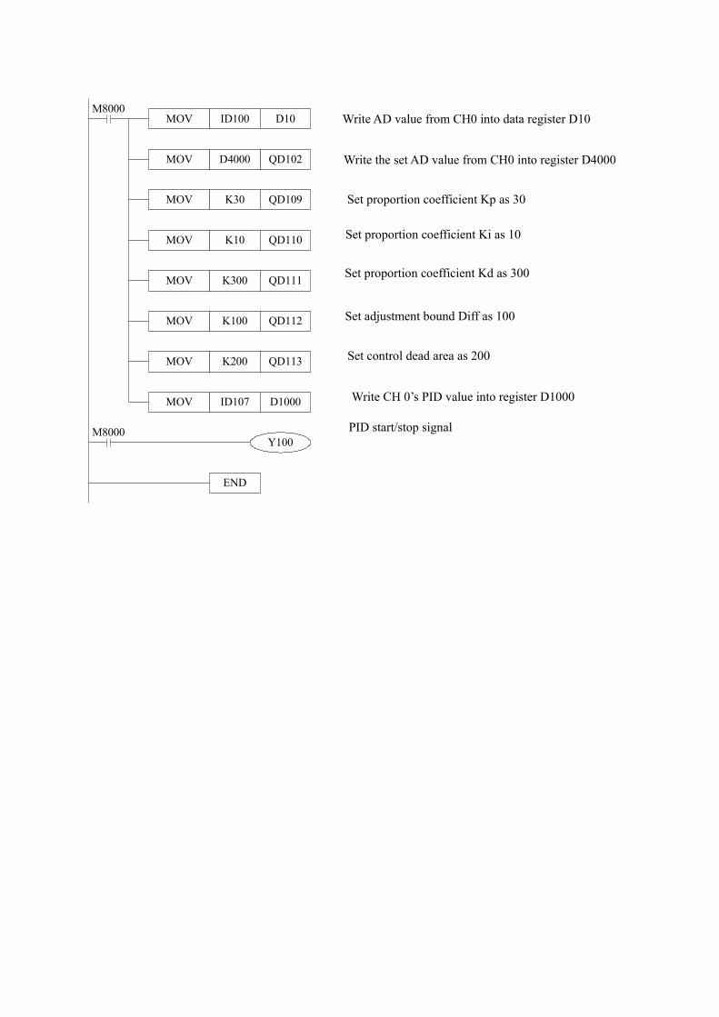
MOV ID100 D10
MOV ID107 D1000
M8000
MOV K30 QD109
MOV K10 QD110
MOV K300 QD111
MOV K100 QD112
MOV K200 QD113
MOV QD102D4000
END
Y100M8000
Write AD value from CH0 into data register D10
Write the set AD value from CH0 into register D4000
Set proportion coefficient Kp as 30
Set proportion coefficient Ki as 10
Set proportion coefficient Kd as 300
Set adjustment bound Diff as 100
Set control dead area as 200
Write CH 0’s PID value into register D1000
PID start/stop signal
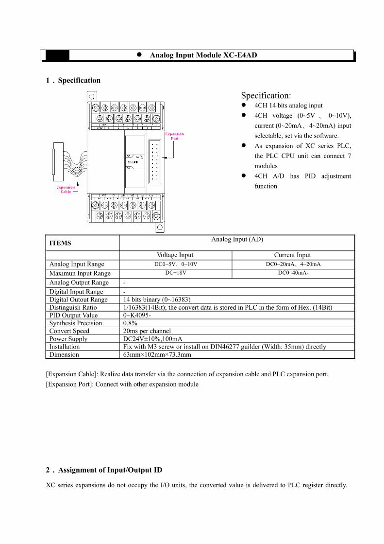
Analog Input Module XC-E4AD
1.Specification
Specification: 4CH 14 bits analog input
4CH voltage (0~5V 、 0~10V),
current (0~20mA、4~20mA) input
selectable, set via the software.
As expansion of XC series PLC,
the PLC CPU unit can connect 7
modules
4CH A/D has PID adjustment
function
ITEMSAnalog Input (AD)
Voltage Input Current Input Analog Input Range DC0~5V、0~10V DC0~20mA、4~20mA
Maximun Input Range DC±18V DC0~40mA-
Analog Output Range -Digital Input Range -Digital Outout Range 14 bits binary (0~16383)Distinguish Ratio 1/16383(14Bit); the convert data is stored in PLC in the form of Hex. (14Bit)PID Output Value 0~K4095-Synthesis Precision 0.8%Convert Speed 20ms per channel Power Supply DC24V±10%,100mAInstallation Fix with M3 screw or install on DIN46277 guilder (Width: 35mm) directly Dimension 63mm×102mm×73.3mm
[Expansion Cable]: Realize data transfer via the connection of expansion cable and PLC expansion port.
[Expansion Port]: Connect with other expansion module
2.Assignment of Input/Output ID
XC series expansions do not occupy the I/O units, the converted value is delivered to PLC register directly.

Analog output is also offered by PLC register.
Register ID of expansion 1:
Channel AD Signal PID Output Value
PID Start/Stop Control Bit
The Set Value PID Parameters: Kp, Ki, Kd, Control Range Diff, Dead Range “Death”
0CH ID100 ID104 Y100 QD102 Kp-------Ki-------
Kd-------
Diff------
Death----
QD106 QD107 QD108QD109
QD110
1CH ID101 ID105 Y101 QD103
2CH ID102 ID106 Y102 QD104
3CH ID103 ID107 Y103 QD105
Register ID of expansion 2:
Channel AD Signal PID Output Value
PID Start/Stop Control Bit
The Set Value PID Parameters: Kp, Ki, Kd, Control Range Diff, Dead Range “Death”
0CH ID200 ID204 Y200 QD202 Kp-------Ki-------
Kd-------
Diff------
Death----
QD206 QD207 QD208QD209
QD210
1CH ID201 ID205 Y201 QD203
2CH ID202 ID206 Y202 QD204
3CH ID203 ID207 Y203 QD205
Register ID of expansion 3:
Channel AD Signal PID Output Value
PID Start/Stop Control Bit
The Set Value PID Parameters: Kp, Ki, Kd, Control Range Diff, Dead Range “Death”
0CH ID300 ID304 Y300 QD302 Kp-------Ki-------
Kd-------
Diff------
Death----
QD306 QD307 QD308QD309
QD310
1CH ID301 ID305 Y301 QD303
2CH ID302 ID306 Y302 QD304
3CH ID303 ID307 Y303 QD305
Register ID of expansion 4:
Channel AD Signal PID Output Value
PID Start/Stop Control Bit
The Set Value PID Parameters: Kp, Ki, Kd, Control Range Diff, Dead Range “Death”
0CH ID400 ID404 Y400 QD402 Kp-------Ki-------
Kd-------
Diff------
Death----
QD406 QD407 QD408QD409
QD410
1CH ID401 ID405 Y401 QD403
2CH ID402 ID406 Y402 QD404
3CH ID403 ID407 Y403 QD405
Register ID of expansion 5:
Channel AD Signal PID Output Value
PID Start/Stop Control Bit
The Set Value PID Parameters: Kp, Ki, Kd, Control Range Diff, Dead Range “Death”
0CH ID500 ID504 Y500 QD502 Kp-------Ki-------
Kd-------
Diff------
Death----
QD506 QD507 QD508QD509
QD510
1CH ID501 ID505 Y501 QD503
2CH ID502 ID506 Y502 QD504
3CH ID503 ID507 Y503 QD505
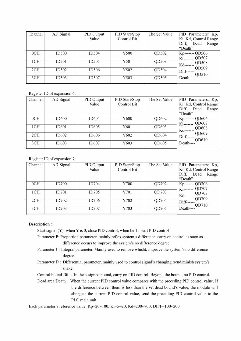
Register ID of expansion 6:
Channel AD Signal PID Output Value
PID Start/Stop Control Bit
The Set Value PID Parameters: Kp, Ki, Kd, Control Range Diff, Dead Range “Death”
0CH ID600 ID604 Y600 QD602 Kp-------Ki-------
Kd-------
Diff------
Death----
QD606 QD607 QD608QD609
QD610
1CH ID601 ID605 Y601 QD603
2CH ID602 ID606 Y602 QD604
3CH ID603 ID607 Y603 QD605
Register ID of expansion 7:
Channel AD Signal PID Output Value
PID Start/Stop Control Bit
The Set Value PID Parameters: Kp, Ki, Kd, Control Range Diff, Dead Range “Death”
0CH ID700 ID704 Y700 QD702 Kp-------Ki-------
Kd-------
Diff------
Death----
QD706 QD707 QD708QD709
QD710
1CH ID701 ID705 Y701 QD703
2CH ID702 ID706 Y702 QD704
3CH ID703 ID707 Y703 QD705
Description:Start signal (Y): when Y is 0, close PID control, when be 1 , start PID control
Parameter P: Proportion parameter, mainly reflex system’s difference, carry on control as soon as
difference occurs to improve the system’s no difference degree.
Parameter I:Integral parameter. Mainly used to remove whisht, improve the system’s no difference
degree. Parameter D:Differential parameter, mainly used to control signal’s changing trend,minish system’s
shake. Control bound Diff:In the assigned bound, carry on PID control. Beyond the bound, no PID control.
Dead area Death:When the current PID control value compares with the preceding PID control value. If
the difference between them is less than the set dead bound’s value, the module will
abnegate the current PID control value, send the preceding PID control value to the
PLC main unit.
Each parameter’s reference value: Kp=20~100; Ki=5~20; Kd=200~700; DIFF=100~200
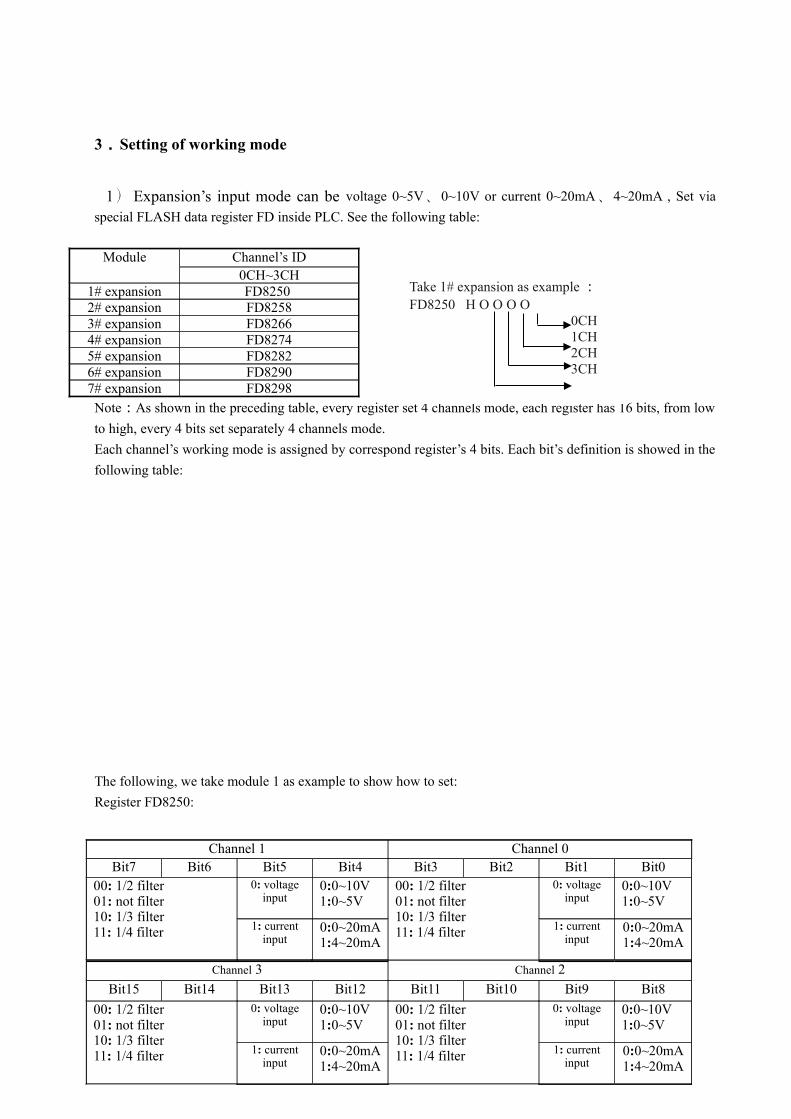
3.Setting of working mode
1)Expansion’s input mode can be voltage 0~5V、0~10V or current 0~20mA 、4~20mA , Set via
special FLASH data register FD inside PLC. See the following table:
Module Channel’s ID0CH~3CH
1# expansion FD8250 2# expansion FD82583# expansion FD82664# expansion FD82745# expansion FD82826# expansion FD82907# expansion FD8298
Note:As shown in the preceding table, every register set 4 channels mode, each register has 16 bits, from low
to high, every 4 bits set separately 4 channels mode.
Each channel’s working mode is assigned by correspond register’s 4 bits. Each bit’s definition is showed in the
following table:
The following, we take module 1 as example to show how to set:
Register FD8250:
Channel 1 Channel 0Bit7 Bit6 Bit5 Bit4 Bit3 Bit2 Bit1 Bit0
00: 1/2 filter01: not filter10: 1/3 filter11: 1/4 filter
0: voltage input
0:0~10V1:0~5V
00: 1/2 filter01: not filter10: 1/3 filter11: 1/4 filter
0: voltage input
0:0~10V1:0~5V
1: current input
0:0~20mA1:4~20mA
1: current input
0:0~20mA1:4~20mA
Channel 3 Channel 2
Bit15 Bit14 Bit13 Bit12 Bit11 Bit10 Bit9 Bit8
00: 1/2 filter01: not filter10: 1/3 filter11: 1/4 filter
0: voltage input
0:0~10V1:0~5V
00: 1/2 filter01: not filter10: 1/3 filter11: 1/4 filter
0: voltage input
0:0~10V1:0~5V
1: current input
0:0~20mA1:4~20mA
1: current input
0:0~20mA1:4~20mA
Take 1# expansion as example :FD8250 H O O O O
0CH1CH2CH3CH

E.g. : 1) If set working mode 0~20mA 、 4~20mA 、 0~10V 、 0~5V of module 1’s channel 3 、 channel
2、channel 1、channel 0, filters are all 1/2 filter, value in FD8250 is 2301H
4.Exterior connection
When carry on external connection, please note the following two items:
When connect+24V power outside, please choose 24V power on PLC main unit to avoid interfere.
To avoid interfere, please use shield cable and single point grounding with the shield layer.
5.Analog digital convert chart
The relationship between input analog and converted digital is showed in the following chart:
0~5V analog input 0~10V analog input
0~20mA analog input 4~20mA analog input

6.Programming
E.g.1 Real time read the 4 channels data, write 2 channels data (take expansion 1 as example)
MOV ID100 D0
END
M8000
MOV ID101 D1
MOV ID102 D2
MOV ID103 D3
MOV D10 QD100
MOV D11 QD101
E.g.2 Applied method of PID (take expansion 1’s channel 0 as example)
0 D0
1 D1
输入第 2 通道的数据写入数据寄存器 D2Write data from CH3 into data register D3
数据寄存器 D10 写入数据给输出第 0 通道
Output data in register D11 to CH1.

MOV ID100 D10
MOV ID104 D1000
M8000
MOV K30 QD106
MOV K10 QD107
MOV K300 QD118
MOV K100 QD119
MOV K200 QD110
MOV QD100D4000
END
Y100M8000
Write channel 0’s data into data register D10
Channel 0’s set value is register D4000
Set proportion coefficient Kp as 30
Set proportion coefficient Ki as 10
Set proportion coefficient Kd as 300
Set adjustment bound Diff as 100
Set control dead area as 200
Write channel 0’s PID output value into register D1000
PID start signal

VIII 、XC-E3AD4PT2DAVIII 、XC-E3AD4PT2DA
1.Specifications
Specilities: 3 channels 14 bits current input 、 4
channels PT100 temperature input and 2
channels 12 bits voltage output
3 channels current 0~20mA 、 4~20mA
input (selectable) and 2 channels voltage
0~5V、0~10V output (selectable), set via
the software
Pt resistor input (PT100)
3 channels A/D and 4 channels PT input,
with PID adjustment function
ITEMSAnalog Current Input
(AD)Temperature Input (PT) Analog Voltage Output
(DA)Analog Input DC0~20mA、4~20mA PT100 -
Temperature Testing Bound
- -100~350℃ -
Maximum Output Bound
DC0~40mA - -
Analog Output Bound - -
DC0~5V、0~10V
External load resistor
(2KΩ~1MΩ)Digital Input Bound
- - 12 bits binary (0~4095)
Digital Output Bound
14 bits binary (0~16383) -1000~3500 -
Distinguish 1/16383(14Bit); the converted data is stored into PLC(14Bit) in the form of Hex.
0.1℃ 1/4095(12Bit); the converted data is stored into PLC(12Bit) in the form of Hex.
PID Output Value 0~K4095 -General Precision
0.8% ±0.5℃ 0.8%
Convert Speed 20ms per channel 3ms per channelPower Supply for Analog Using
DC24V±10%,100mA
Installation Fix with M3 screws or install on DIN46277 (Width: 35mm) leader directly Dimension 63mm×102mm×73.3mm
[Extend Cable]: Via the connection of the extend cable and PLC’s extend port, realize data transfer
[Extend Port]: Connect with other expansions
2. Input/Output Definition
XC series analog modules do not engross I/O units, the converted value is sent to PLC register
directly. Analog output is also offered by PLC register.
The first expansion’s register definition: Channel AD Signal PID Output
Value PID start/stop
bitThe Set Value PID : Kp, Ki, Kd,
Diff, Death0CH ID100 ID107 Y100 QD102 Kp-------
Ki-------
Kd-------
Diff------
Death----
QD109 QD110 QD111QD112
QD113
1CH ID101 ID108 Y101 QD103
2CH ID102 ID109 Y102 QD104
Channel PT Signal PID Output Value
PID start/stop bit
The Set Value
3CH ID103 ID110 Y103 QD105
4CH ID104 ID111 Y104 QD106
5CH ID105 ID112 Y105 QD107
6CH ID106 ID113 Y106 QD108
Channel DA Signal - - - -0CH QD100 - - -1CH QD101 - - -
The second expansion’s register definition:Channel AD Signal PID Output
Value PID start/stop
bitThe Set Value PID : Kp, Ki, Kd,
Diff, Death0CH ID200 ID207 Y200 QD202 Kp-------
Ki-------
Kd-------
Diff------
Death----
QD209 QD210 QD211QD212
QD213
1CH ID201 ID208 Y201 QD203
2CH ID202 ID209 Y202 QD204
Channel PT Signal PID Output Value
PID start/stop bit
The Set Value
3CH ID203 ID210 Y203 QD205
4CH ID204 ID211 Y204 QD206
5CH ID205 ID212 Y205 QD207
6CH ID206 ID213 Y206 QD208
Channel DA Signal - - - -0CH QD200 - - -1CH QD201 - - -
The third expansion’s register definition:
Channel AD Signal PID Output Value
PID start/stop bit
The Set Value PID : Kp, Ki, Kd, Diff, Death
0CH ID300 ID307 Y300 QD302 Kp-------Ki-------
Kd-------
Diff------
Death----
QD309 QD310 QD311QD312
QD313
1CH ID301 ID308 Y301 QD303
2CH ID302 ID309 Y302 QD304
Channel PT Signal PID Output Value
PID start/stop bit
The Set Value
3CH ID303 ID310 Y303 QD305
4CH ID304 ID311 Y304 QD306
5CH ID305 ID312 Y305 QD307
6CH ID306 ID313 Y306 QD308
Channel DA Signal - - - -0CH QD300 - - -1CH QD301 - - -
The fourth expansion’s register definition:Channel AD Signal PID Output
Value PID start/stop
bitThe Set Value PID : Kp, Ki, Kd,
Diff, Death0CH ID400 ID407 Y400 QD402 Kp-------
Ki-------
Kd-------
Diff------
Death----
QD409 QD410 QD411QD412
QD413
1CH ID401 ID408 Y401 QD403
2CH ID402 ID409 Y402 QD404
Channel PT Signal PID Output Value
PID start/stop bit
The Set Value
3CH ID403 ID410 Y403 QD405
4CH ID404 ID411 Y404 QD406
5CH ID405 ID412 Y405 QD407
6CH ID406 ID413 Y406 QD408
Channel DA Signal - - - -0CH QD400 - - -1CH QD401 - - -
The fifth expansion’s register definition:Channel AD Signal PID Output
Value PID start/stop
bitThe Set Value PID : Kp, Ki, Kd,
Diff, Death0CH ID500 ID507 Y500 QD502 Kp-------
Ki-------
Kd-------
Diff------
Death----
QD509 QD510 QD511QD512
QD513
1CH ID501 ID508 Y501 QD503
2CH ID502 ID509 Y502 QD504
Channel PT Signal PID Output Value
PID start/stop bit
The Set Value
3CH ID503 ID510 Y503 QD505
4CH ID504 ID511 Y504 QD506

5CH ID505 ID512 Y505 QD507
6CH ID506 ID513 Y506 QD508
Channel DA Signal - - - -0CH QD500 - - -1CH QD501 - - -
The sixth expansion’s register definition:Channel AD Signal PID Output
Value PID start/stop
bitThe Set Value PID : Kp, Ki, Kd,
Diff, Death0CH ID600 ID607 Y600 QD602 Kp-------
Ki-------
Kd-------
Diff------
Death----
QD609 QD610 QD611QD612
QD613
1CH ID601 ID608 Y601 QD603
2CH ID602 ID609 Y602 QD604
Channel PT Signal PID Output Value
PID start/stop bit
The Set Value
3CH ID603 ID610 Y603 QD605
4CH ID604 ID611 Y604 QD606
5CH ID605 ID612 Y605 QD607
6CH ID606 ID613 Y606 QD608
Channel DA Signal - - - -0CH QD600 - - -1CH QD601 - - -
The seventh expansion’s register definition:Channel AD Signal PID Output
Value PID start/stop
bitThe Set Value PID : Kp, Ki, Kd,
Diff, Death0CH ID700 ID707 Y700 QD702 Kp-------
Ki-------
Kd-------
Diff------
Death----
QD709 QD710 QD711QD712
QD713
1CH ID701 ID708 Y701 QD703
2CH ID702 ID709 Y702 QD704
Channel PT Signal PID Output Value
PID start/stop bit
The Set Value
3CH ID703 ID710 Y703 QD705
4CH ID704 ID711 Y704 QD706
5CH ID705 ID712 Y705 QD707
6CH ID706 ID713 Y706 QD708
Channel DA Signal - - - -0CH QD700 - - -1CH QD701 - - -
Description:Start signal (Y): when Y is 0, close PID control, when be 1 , start PID control
Parameter P:Proportion parameter, mainly reflex system’s difference, carry on control as soon
as difference occurs to improve the system’s no difference degree.
Parameter I:Integral parameter. Mainly used to remove whisht, improve the system’s no
difference degree.
Parameter D:Differential parameter, mainly used to control signal’s changing trend,minish
system’s shake.
Control bound Diff: In the assigned bound, carry on PID control. Beyond the bound, no PID
control.
Dead area Death:When the current PID control value compares with the preceding PID control
value. If the difference between them is less than the set dead bound’s value,
the module will abnegate the current PID control value, send the preceding
PID control value to the PLC main unit.
Each parameter’s reference value:Kp=20~100;Ki=5~20;Kd=200~700;DIFF=100~200
3.Working Mode Setting
1)Expansion’s input/output mode can be set via special FLASH data register FD inside PLC.
Module Register’s ID
1# Module FD8250 、FD8251、FD8252 2# Module FD8258、FD8259、FD8260 3# Module FD8266、FD8267、FD82684# Module FD8274、FD8275、FD82765# Module FD8282、FD8283、FD82846# Module FD8290、FD8291、FD82927# Module FD8298、FD8299、FD8270
Each bit’s definition is showed in the following table:
The following, we take module 1 as the example to show how to set:
Take 1# module as the example: FD8250 H O O O O
0CH ( AD )
1CH ( AD )
2CH ( AD )
3CH ( PT )FD8251 H O O O O
4CH ( PT )
5CH ( PT )
6CH ( PT )
0CH ( DA )
FD8252 H O O O O
1CH ( DA )
Note : As showed in the preceding table, each register set 4 channels’ mode, each register has 16 bits. From low bit to high bit, every 4 bits separately set 4 channels’ mode.

Register FD8250:
Low byte of register FD8251::
Low byte of register FD8252:
4.External Connection
Please note the following two items about external connection:
When connect with external +24V power supply, please use 24V power supply on PLC main unit to
avoid intefere
To avoid intefere, please use shield cable, and single-point grounding with the shield layer.
Input CH 1 (AD) Input CH 0(AD)Bit7 Bit6 Bit5 Bit4 Bit3 Bit2 Bit1 Bit0
00: 1/2 filter01: not filter10: 1/3 filter11: 1/4 filter
- 0:0~20mA1:4~20mA
00: 1/2 filter01: not filter10: 1/3 filter11: 1/4 filter
- 0:0~20mA1:4~20mA
Input CH 3(PT) Input CH 2(AD)Bit15 Bit14 Bit13 Bit12 Bit11 Bit10 Bit9 Bit8
00: 1/2 filter01: not filter10: 1/3 filter11: 1/4 filter
- 00: 1/2 filter01: not filter10: 1/3 filter11: 1/4 filter
- 0:0~20mA1:4~20mA
Input CH 5(PT) Input CH 4(PT)Bit7 Bit6 Bit5 Bit4 Bit3 Bit2 Bit1 Bit0
00: 1/2 filter01: not filter10: 1/3 filter11: 1/4 filter
- 00: 1/2 filter01: not filter10: 1/3 filter11: 1/4 filter
-
Output CH 0(DA) Input CH 6(PT)Bit15 Bit14 Bit13 Bit12 Bit11 Bit10 Bit9 Bit8
- 0 :0~10V1 :0~5V
00: 1/2 filter01: not filter10: 1/3 filter11: 1/4 filter
-
- Output CH 1(PT)Bit7 Bit6 Bit5 Bit4 Bit3 Bit2 Bit1 Bit0
- - - - - 0 :0~10V1 :0~5V

Module’s 0~20mA or 4~20mA output should be offered 24V power supply from outside. According to the
QD value, adjust the circuit’s current. The module itself doesn’t generate current.
0V24V+ AI0+AI0- AI1+AI1- AI2+AI2- VO0+VO0- VO1+VO1-
C0AI 0
C1 C3VO1AI 2
C2 C4VO0AI 1
B3C3
A0B0 C1
C0 B1 A2 C2A3B2A1
PWR
A
A
PT100 PT10
0 PT100
PT100
5.Analog/Digital convert Diagram
The relationship of the input analog quantity and the converted digital quantity is shown below:
0~20mA analog input 4~20mA analog input
The relationship of the output digital quantity and its correspond analog quantity is shown below:
0~5V analog output 0~10V analog output
When the output value is larger than K4095, D/A converted analog value will remain 5V、10V.
The output specialty of PT100 is shown below:
PT100 Input

6.Program
E.g. 1)Real time read data from 7 channels, write data to 2 channels (take module 1 as the example)
MOV ID100 D0
END
M8000
MOV ID101 D1
MOV ID102 D2
MOV ID103 D3
MOV D10 QD100
MOV D11 QD101
MOV ID104 D4
MOV ID105 D5
MOV ID106 D6
Write AD value in CH0 to data register D0
Write AD value in CH1 to data register D1
Write AD value in CH2 to data register D2
Write temperature value in CH3 to data register D3
Output value in register D10 to CH0
Output value in register D11to CH0
Write temperature value in CH4 to data register D4
Write temperature value in CH5 to data register D5
Write temperature value in CH6 to data register D6

E.g.2) Application of PID (Take CH0 of module 1 as the example)
MOV ID100 D10
MOV ID107 D1000
M8000
MOV K30 QD109
MOV K10 QD110
MOV K300 QD111
MOV K100 QD112
MOV K200 QD113
MOV QD102D4000
END
Y100M8000
\
Write AD value from CH0 into data register D10
Write the set AD value from CH0 into register D4000
Set proportion coefficient Kp as 30
Set proportion coefficient Ki as 10
Set proportion coefficient Kd as 300
Set adjustment bound Diff as 100
Set control dead area as 200
Write CH 0’s PID value into register D1000
PID start/stop signal

IX 、XC-E2DAIX 、XC-E2DA
1. Specifications Characteristic:● 12 bits high precision analog
input.
● 2 channels selectable voltage
0 to 5V, 0 to 10 V, currents
are 0 to 20mA, 4 to 20 mA
output (selectable)
● As special function module
of XC series, 7 modules
could be connected at most
Items Voltage output Current outputAnalog input DC 0 to 5V, 0 to 10V DC0 to 20mA, 4 to
20mADigital output 12 bits 2HDistinguish 1/4096(12 bit); the cover data is stored into
PLC in the form of HexGeneral precision 0.8%Convert speed 3ms per channelIsolation DC/AC convert, optical-coupling isolatePower supply for analog using DC24V±10%,100mAInstallation Fix with M3 screws or install on DIN46277
(width: 35) leader directlyDimension 63mm×102mm×73.3mm[extend cable]:via the connection of the extend cable and PLC’s extend port, realize data transfer.
[extend port]: connect with other expansions.
2. The assignment of input/output IDFC series analog modules don’t engross I/O units, the converted value is sent to PLC register directly.
Analog output is also offered by PLC register.
Register’s ID of expansion 1:Channel 1 unit 2 unit 3 unit 4 unit 5 unit 6 unit 7 unit0CH QD100 QD200 QD300 QD400 QD500 QD600 QD7001CH QD101 QD201 QD301 QD401 QD501 QD601 QD701
3.Setting of working module
1) Expansion module input/output voltage is 0 to 5V, 0 to 10V, current is 0 to 20mA, 4 to 20mA module
selectable, via PLC internal special FLASH registers FD setting. Such as follows:

Modules Channels No.0CH to 1CH
1#modules D82502#modules D82543#modules D82584#modules D82625#modules D82646#modules D82687#modules D8272Note: As show in the preceding table, each register set 2 channels’ mode, each register has 16 bits, from low
bit to high bit, every 4 bits set 2 channels’ mode.
Take the first module as an example:
Register FD8250:Channel 1 Channel 0
Bit7 Bit6 Bit5 Bit4 Bit3 Bit2 Bit1 Bit0- 0:voltage
output0:0 to 10V
1:0 to 5V
- 0:voltage output
1:current output
0:0 to 20mA1:4 to
20mA
1:current output
3. External connectionWhen carry on exterior connection, please note the following two items:
● When connect with external +24V power supply, please use 24V power supply on PLC main unit to avoid
intefere.
● To avoid intefere, please use shield cable, and single-point grounding with the shield layer.
● Module’s 0 to20 mA or 4 to 20mA output should be offered 24V power supply from outside. According to
the OD value. Adjust the circuit’s current. The module itself doesn’t generate current.
Take 1# module as a example:FD8250 H 0 0 0 0
0CH
1CH

4. Analog/Digital convert DiagramThe relationship of the input analog quantity and the converted digital quantity is shown below.
When the output value is larger than K4095, D?A converted analog value will remain 5V, 10V or 20mA.
6. Program eg.1) Real time write data to 2 channels

Write register D10’s value into specification channel 0
Write register D11’s value into specification channel 1

Thinget Electronic Co., Ltd.
4th Floor Building 7,Orignality Industry
park, Liyuan Development Zone, Wuxi
City, Jiangsu Province 214072
Tel: (510)85134136
Fax: (510)85111290