what about switched capacitor...
TRANSCRIPT

What About Switched Capacitor Converters?
Grad Students: Michael Seeman, Vincent Ng, andHanh-Phuc
Le
Profs. Seth Sanders and Elad
AlonEECS Department, UC Berkeley

Switched Capacitor Power Converters
•
Only switches and capacitors •
Simple low freq model as an ideal transformer with Thevenin
impedance–
neglects freq dependent loss and leakage–
Would model leakage, dynamic losses with shunt imped.
•
Using no inductors has advantages:–
Simplified full integration potential–
Works well over a wide power range•
Single mode, can adjust clock rate•
No minimum load–
No inductive switching losses•
Open-loop loadline
regulation:–
Output impedance has R-C characteristic, with R naturally designed to meet efficiency spec

Why Not S-C ?
•
Difficult regulation?•
Not suited for high current/power?
•
Lots of difficult gate drive details?•
Interconnect difficulty for many caps?
•
Voltage rating of CMOS processes?•
Magnetic-based ckts
= higher performance?

SC Analysis: Simplest Example
•
Slow Switching Limit (SSL):–
Impulsive currents (charge transfers)–
Resistance negligible (assume R = 0)–
This (SSL) impedance is the switching loss!•
Fast Switching Limit (FSL):–
Constant current through switches–
Model capacitors as voltage sources (C → ∞)
vCfqfi swsw Δ=Δ=
vR
i Δ=1
41
)( OUTIN VVv −=Δ
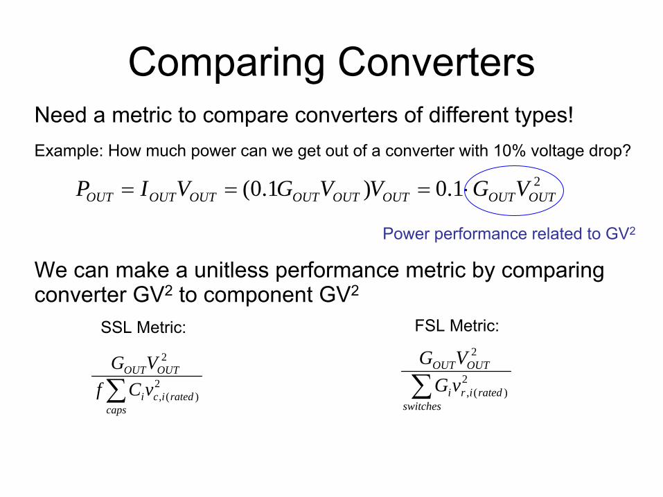
Comparing ConvertersNeed a metric to compare converters of different types!Example: How much power can we get out of a converter with 10% voltage drop?
21.0)1.0( OUTOUTOUTOUTOUTOUTOUTOUT VGVVGVIP ⋅===
Power performance related to GV2
We can make a unitless
performance metric by comparing converter GV2
to component GV2
SSL Metric: FSL Metric:
∑caps
ratedici
OUTOUT
vCfVG
2)(,
2
∑switches
ratediri
OUTOUT
vGVG
2)(,
2

Analysis via Charge Multipliers
phasesboth flow, chargeoutput phase , capin flow charge
,jia j
ic =
phasesboth flow, chargeoutput on when ,switch in flow charge
,ia ir =
Phase 1:
Phase 2:
211 =ca
21
1, =ra
21
3, −=ra
212 −=ca
21
2, =ra
21
4, −=ra
Capacitor Charge Multiplier:
Switch Charge Multiplier:

Output Impedance ~ Power Loss M. Seeman, S. Sanders, IEEE T-PELS, March 2008
•
An SC converter’s power loss is the sum of component energy (power) losses:
•
The converter’s output impedance can be determined in terms of just the charge multiplier components:
2OUTSSL
capacitorsiiswSSL iRvqfP =ΔΔ= ∑ ( )∑=
switchesswiiFSL fqRP 22
21
∑=capacitors swi
icSSL fC
aR
2, )( 2
, )(2 ∑=switches
iriFSL aRR
7

Output Impedance and OptimizationTellegen’s
theorem and energy conservation used to find ROUT
:
∑∈
=capacitorsi i
ic
swOUT C
af
R21
, )(1 ∑∈
=switchesi
iriOUT aRR 2, )(2SSL: FSL:
Minimize output impedance while keeping component cost constant:
)(,
,*
ratedic
ici v
aC ∝
2
)(,,*
21
⎟⎟⎠
⎞⎜⎜⎝
⎛= ∑
capacitorsratedicic
swTOTSSL va
fER
)(,
,*
ratedir
iri v
aG ∝
2
)(,,* 2
⎟⎠
⎞⎜⎝
⎛= ∑
switchesratedirir
TOTFSL va
AR
∑=capacitors
ratediciTOT vCE 2)(,2
1
∑=switches
ratediriTOT vGA 2)(,
Cost constraint Optimizedcomponents
Optimized output impedance
In the optimal case:Capacitor voltage ripple and switch voltage drop are proportional to rated voltageOutput impedance proportional to the square of the sum of the component V-A products

Comparison with Magnetic Designs
Switch sizes optimized for a given conversion ratio n for all converters
Boost or Buck converter
Transformer-bridge converter
Ladder-type switched-
cap converter

•Performance compared with switch GV2 metric:
•Magnetic components modeled with zero conduction loss, and no switching loss impact
Switch Utilization –
Conduction Loss Comparison
Ideal transformer ckt: 1/32
Boost/buck
Ladder/Dickson∑ 2
)(,
2
ratediri
OUTOUT
vGVG

D.H. Wolaver, PhD dissertation,MIT,1969 proves fundamental thms
on dc-dc conv.:
•
Switches (resistors):
•
Ladder/Dickson are optimal
•
Reactive Elements:
Okactivedck
k PG
Giv 1−≥− ∑
−∈( ) ( ) Okk
activeackkk P
GGiivv 1−
≥−•−− ∑−∈
Oreactivek
kk PG
Giv 121 −
≥∑∈
OLk
kkCk
kk PG
Gf
IqV 11 −≥+∑∑
∈∈
λMeaning for 2-phase ckts:
G = voltage or current gain

Utilization of Reactive Elements:•For boost or buck, derate
inductor by 1000x relative to cap
due to practical energy density, assert that S-C examples exhibit 2% voltage drop relative to mag
ckts

The Submicron Opportunity
•
Rate device by ratio:–
Essentially an Ft type parameter for a power switch reflecting power gain, exposes opportunity in scaling
•
Suggests that we should look for opportunities to build our ckts
with scaled CMOS based devices,
but:–
Low voltage rating per device
–
Inadequate metal/interconnect for high current?
22gss CVVG

Regulation Considerations•
Open-Loop Loadline
Regulation
–
Droop matching resistive output impedance effective for loadline
VR type reg.
•
Tap Changing for Line Regulation –
Feedforward•
Multi-mode Operation for Apps like Voltage Scaling
Dominant First Order Dynamics
Simulation Example: 8-phase 2-to-1 converter

Example 1 –
Point-of-Load:12V-to-1.5V Dickson Circuit
15
V.W. Ng, A 98% peak efficiency 1.5A 12V-to-1.5V Switched Capacitor dc-dc converter in 0.18 um CMOS technology, Master Thesis Report, EECS Dept, UC Berkeley, Dec. 2007.
Illustrates “tap-changing”
technique for line regulation.

Layout in Triple-Well 0.18 um CMOS
16

Design vs. Performance

POL Design 2: Flip Chip Packaging Scheme

Cost and PCB Area Comparison

Ex. 2 -
Ultra-low-power Conversion in PicoCube
Wireless Sensor Node
Shaker
15mahNiMH 1.0 - 1.4v
2.0 – 2.8v
chargepump
radio PA power enable analog switch
0.65v1.0vRadio digital power(GPIO pin)
MSP430uC
SPI serial IF
Wakeup
JTAG external IF
TPMSSensor
powerswitches
SPI VDD
Tx VDD
SPI serial IF
Tx datalevel
shifters
Interface
radio
RF
SPI pwr on/off
PA pwr on/off
SPI serial IF
Tx data
Sensor/Digital
shunt regulator
linearregulator
PicoCubePower IC
Reduced Quiescent Power
Smaller Size
Greater Efficiency
PicoCube: A 1cm3 Sensor Node Powered by Harvested Energy, 2008 DAC/ISSCC
Student Design Contest

PicoCube
Power Management Chip Block Diagram
SynchronousRectifier
0.7V (3:2) Converter
VoltageReference
CurrentReference
2.1V (1:2) Converter
LinearRegulators
Feedback
Battery
Shaker
Radio
MicrocontrollerSensors
Analog/Control Circuits Power Circuits
Seeman, Sanders, Rabaey, “An Ultra-Low-Power Power Management IC for Wireless Sensor Nodes,”
CICC 2007.

PicoCube Converter Topology
Linear Regulators (LDOs) further regulate and reduce ripple on outputs
PicoRadio
Level shifters
Microcontroller + sensors
3:2 converter1:2 converter

Hysteretic Feedback
•
Regulates output voltage–
On/off clocking control
–
Thermostat-type control
–
Improves efficiency by reducing fsw
for small loads
1 MΩ
1 MΩ2 kΩ
270 Ω
Converter leaves regulation for only large loads
10 kΩ 1 MΩ

Converter Performance
Regulation is effective at controlling output voltage and increasing efficiency at low power levels!
Regulated
Unregulated Regulated
Unregulated
VDD
= 1.144V

Ex. 3: Microprocessor SC Converter
•
A power density of 1 W/mm2
is achievable in 65nm process.•
A tiled design improves output ripple and ESR performance•
Creates a scalable IP platform•
Ideal for microprocessor supplies:–
Ultra-fast transient response–
Package I/O at higher voltage/lower current–
Independent core voltage control
Core1
P1a
P1d
P1cP1b Core
2
P2a
P2d
P2cP2b
Core4
P4a
P4d
P4cP4b Core
5
P5a
P5d
P5cP5b
Core3
P3a
P3d
P3cP3b
Core6
P6a
P6d
P6cP6b
Core7
P7a
P7d
P7cP7b Core
8
P8a
P8d
P8cP8b Core
9
P9a
P9d
P9cP9b

Design Optimization Example: 0.4 W/sq.mm
•
Representative 0.13um tech
•
2.4-to-1.2V Conversion•
1 sq mm M-I-M cap (2 nF)•
Losses –
SSL (main caps)–
FSL (conduction)–
Gate cap–
Cap Bottom plate–
Junction cap

Switched Cap Take-Aways
•
Theoretical performance exceeds magnetic-based converters, and this is being realized in research
•
Very simple low power operation –
reduce clk•
Integration convenient for v. low power app’s to v. high current app’s
•
Moderate (high) voltage capability by stacking devices – triple-well, SOI
•
Regulation challenges –
nominal fixed ratio, but can operate with multiple Taps
•
Further on-chip integration via aggressive clk
scaling

•
Tap Changing for Line Regulation – Feedforward
•
Multi-mode Operation for Apps like Voltage Scaling

Conduction Loss Comparison M. Seeman, S. Sanders, IEEE T-PELS, March 2008
∑ 2)(,
2
ratediri
OUTOUT
vGVG
•Performance compared with switch GV2
metric:
•Since converters are bi-
directional, graph applies equally to step-down converters
•Magnetic components modeled with zero conduction loss, and no switching loss impact