vol. 2, issue 2, february 2014 design of different ... of different demultiplexers for wavelength...
TRANSCRIPT

ISSN(Online): 2320-9801 ISSN (Print): 2320-9798
International Journal of Innovative Research in Computer and Communication Engineering
(An ISO 3297: 2007 Certified Organization)
Vol. 2, Issue 2, February 2014
Copyright to IJIRCCE www.ijircce.com 3001
Design of Different Demultiplexers for Wavelength Division Multiplexing Systems
Based On Photonic Crystal Waveguide Dinesh Bhatia1, Nikhil Deep Gupta2
Assistant Professor, Department of Electronics and Communication Engineering, Poornima Institute of Engineering & Technology, Jaipur, India1
Research Scholar, Department of Electronics and Communication Engineering, Malaviya National Institute of Technology (MNIT), Jaipur, India2
ABSTRACT: Waveguides made up of photonic crystals have some unique properties such as air core guidance with band gap effect, effective refractive index guidance etc. These unique properties have their direct dependence on the degree of freedom associated with photonic crystals. This degree of freedom allows us to use these waveguides as de-multiplexers by creating defects within the waveguides. The work is concerned about the design and simulation of different de-multiplexers based on photonic crystal waveguide by creating different types of defects within the waveguide.
Keywords: Photonic Crystal, demultiplexer, filter, channel spacing, quality factor, crosstalk
I. INTRODUCTION Photonic crystal is a periodic arrangement of different refractive index materials and this arrangement can be one, two or three dimensional known as 1D, 2D or 3D photonic crystal respectively [1]. Defect in these crystals create a gap of frequency band and photons which have the frequency within this forbidden gap are not allowed to pass through the crystal structure and hence this property of photonic crystal allows us to guide the light along the defect efficiently in photonic communication [2-7]. Light in dielectric medium travels much faster than electrons in metal and this gives the optical communication the ability to transmit data at a very high speed. Apart from that significant bandwidth is offered by the dielectric material as compared to its electrical counterpart, making the high bit rate data transmission possible. As far as energy loss is concern, the optical communication outclasses the electrical communication on this point as well, because of less interaction of light particle as compare to electrons [8].
State of the art integrated circuits have very high density integration and the IC manufacturing companies have a big challenge ahead to further enhance the performance of ICs. Increment in number of transistors results in the increment in heat dissipation and consequently vulnerability of the ICs. The speed of these electronic circuits can be increased at the cost of complexity and reliability. Use of photonic crystals in optical communication has revolutionized the communication totally by providing much faster computing, massive parallel processing, and a new step in digital age [9, 10].
Wavelength division multiplexing is the key component in modern optical communication systems. In this article, a novel concept for a wavelength demultiplexer is proposed and investigated. It utilizes the filtering properties of photonic crystal structure and based on a shift of the cutoff frequency of the photonic band gap mode in a planar photonic crystal waveguide. The rest of this article is organized as follows. Section 2 concentrates on numerical modeling techniques of photonic crystal design. Section 3 concentrates on the modeling and simulation results of different photonic crystal de-multiplexers for wavelength division multiplexing systems. Finally, some conclusions are drawn in Section 4.

ISSN(Online): 2320-9801 ISSN (Print): 2320-9798
International Journal of Innovative Research in Computer and Communication Engineering
(An ISO 3297: 2007 Certified Organization)
Vol. 2, Issue 2, February 2014
Copyright to IJIRCCE www.ijircce.com 3002
II. NUMERICAL MODELING TECHNIQUES There are various numerical modeling techniques for the modeling of photonic devices such as Beam Propagation Method, Finite-Element Method, Finite-Difference Time-Domain (FDTD) Method, Finite-Volume Time-Domain Method, Finite Integration Technique, Multi-resolution Time-Domain Method, Plane Wave Expansion (PWE) Method, etc. However, only few techniques have shown great popularity in the area of research like FDTD and PWE method [11]. In this research work OptiFDTD, design tool of Optiwave Systems Inc., has been used, which utilizes the concept of finite-difference time-domain (FDTD) algorithm. A. PLANE WAVE EXPANSION (PWE) Method In this research work the location and size of the band gap are calculated by Plane wave expansion method. For calculating band structure the plane wave expansion method uses an eigen formulation of the Maxwell's equations. Hence solved for the eigen frequencies for every propagation direction of the wave vectors. The solution directly provides the dispersion diagram.
The Maxwell equation in a transparent, source free, time-invariant, and non-magnetic medium can be represented by the following equation: ∇ ×
∈( ⃗)∇ × 퐻⃗(푟⃗) = 퐻⃗(푟⃗) (1)
where ∈ (푟⃗) is the dielectric function dependent on space vector, c is velocity of light in vacuum, and 퐻⃗(푟⃗) is the optical magnetic field vector of a certain frequency 휔 which has the dependency on time given by 푒 . This equation is sometimes referred as master equation [12], and represents a Hermitian eigen-problem, which would not be applicable if this wave equation would have been derived in terms of the electric field. According to the Bloch theorem the infinite periodicity causes the magnetic field to take the form [11]:
퐻⃗(푟⃗) = 푒 ⃗ ⃗ ℎ⃗(푟⃗) (2) where ℎ⃗(푟⃗) = ℎ⃗ 푟⃗ + 푅⃗ for all combinations of lattice vectors. Thus, master equation in operator form will be represented by following equation:
(∇ + 푖푘)⃗ ×∈( ⃗)
∇ + 푖푘⃗ × ℎ⃗ = ℎ⃗ (3) This represents the fundamental equation, which should be solved. By solving the magnetic field employing simple plane waves in a finite domain, this fundamental equation turns into a finite problem. To solve the final discretized problem different approaches can be explored, e.g. Block-iterative frequency-domain methods [13] and Simple plane wave implementation for photonic crystal [14]. The dispersion relationship between the modes frequencies and the wave vector 푘⃗ is given by the solution of discretized problem, which is also known as band diagram.
III. SIMULATION AND RESULTS The proposed wavelength de-multiplexers are designed by using wavelength-selective filtering property of photonic crystal structures. These proposed wavelength demultiplexers are designed and optimized by finite difference time domain (FDTD) method and the band gap of proposed demultiplexers are calculated by using plane wave expansion (PWE) method. A. Design of filter We have designed 2-D Photonic Crystal of square lattice with identical rods. The refractive index of rods is 3.47 (Si rods) and the radius of rods are taken as 0.18a (where ‘a’ is lattice constant). Optical filters are the basis of proposed wavelength demultiplexers. Some point defects are created in the photonic crystal structure to generate these optical filters.
ISSN(Online): 2320-9801 ISSN (Print): 2320-9798
International Journal of Innovative Research in Computer and Communication Engineering
(An ISO 3297: 2007 Certified Organization)
Vol. 2, Issue 2, February 2014
Copyright to IJIRCCE www.ijircce.com 3003
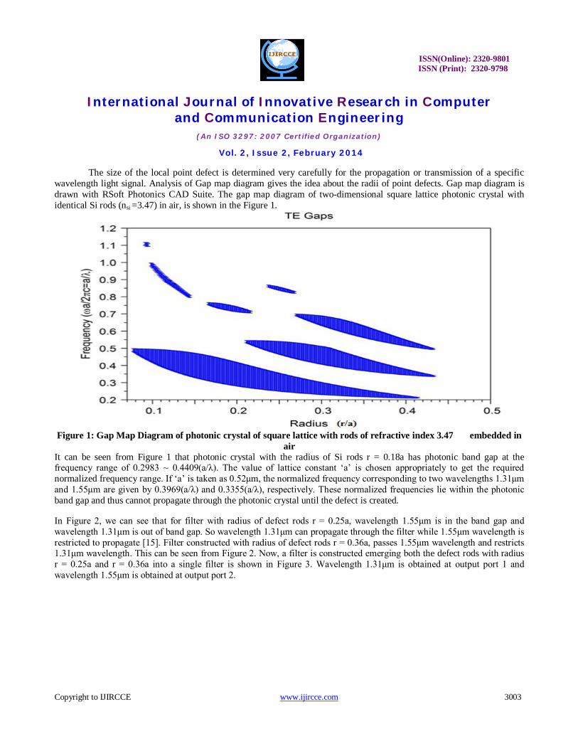
The size of the local point defect is determined very carefully for the propagation or transmission of a specific wavelength light signal. Analysis of Gap map diagram gives the idea about the radii of point defects. Gap map diagram is drawn with RSoft Photonics CAD Suite. The gap map diagram of two-dimensional square lattice photonic crystal with identical Si rods (nsi =3.47) in air, is shown in the Figure 1.
Figure 1: Gap Map Diagram of photonic crystal of square lattice with rods of refractive index 3.47 embedded in
air It can be seen from Figure 1 that photonic crystal with the radius of Si rods r = 0.18a has photonic band gap at the frequency range of 0.2983 ~ 0.4409(a/λ). The value of lattice constant ‘a’ is chosen appropriately to get the required normalized frequency range. If ‘a’ is taken as 0.52μm, the normalized frequency corresponding to two wavelengths 1.31μm and 1.55μm are given by 0.3969(a/λ) and 0.3355(a/λ), respectively. These normalized frequencies lie within the photonic band gap and thus cannot propagate through the photonic crystal until the defect is created.
In Figure 2, we can see that for filter with radius of defect rods r = 0.25a, wavelength 1.55μm is in the band gap and wavelength 1.31μm is out of band gap. So wavelength 1.31μm can propagate through the filter while 1.55μm wavelength is restricted to propagate [15]. Filter constructed with radius of defect rods r = 0.36a, passes 1.55μm wavelength and restricts 1.31μm wavelength. This can be seen from Figure 2. Now, a filter is constructed emerging both the defect rods with radius r = 0.25a and r = 0.36a into a single filter is shown in Figure 3. Wavelength 1.31μm is obtained at output port 1 and wavelength 1.55μm is obtained at output port 2.

ISSN(Online): 2320-9801 ISSN (Print): 2320-9798
International Journal of Innovative Research in Computer and Communication Engineering
(An ISO 3297: 2007 Certified Organization)
Vol. 2, Issue 2, February 2014
Copyright to IJIRCCE www.ijircce.com 3004
Figure 2: r=0.25a and 0.36a are radius of defect rods lying in the band gap corresponding to wavelength 1.31μm and 1.55μm for desired filter.
Figure 3: Filter for wavelength 1.31μm and 1.55μm

ISSN(Online): 2320-9801 ISSN (Print): 2320-9798
International Journal of Innovative Research in Computer and Communication Engineering
(An ISO 3297: 2007 Certified Organization)
Vol. 2, Issue 2, February 2014
Copyright to IJIRCCE www.ijircce.com 3005
(a) (b)
Figure 4(a): Power measured at output port 1(blue) and output port 2(red) for input wavelength 1.31μm.
Figure 4(b): Power measured at output port 1(blue) and output port 2(red) for input wavelength 1.55μm.
Figure 5: Band gap corresponding to photonic crystal structure for different radius of rods
Figure 4 (a) and (b) shows the power at output port 1 and 2 respectively for the input power 1. In the Gap Map shown in Figure 5 we can see that at radius r1 the frequency λ1’ is out of gap map. So it will
propagate through the photonic crystal structure of r1 radius of rods. At radius r1 frequency λ2’ and λ3’ is in the Gap Map. So these frequency will not propagate through the Photonic crystal structure with radius of rods r1.Now decreasing the radius of rods to r2, frequency λ2’ and λ1’ are out of Gap map. So these frequency will propagate through the photonic crystal of rods having radius r2.Again at lowest radius r3, frequency λ3’, λ2’ and λ1’ are out of Gap map. So these frequencies will propagate through Photonic crystal structure of radius r3.
The dispersion curves of photonic crystal (r = 0.18a) for different radius of defect were calculated by plane wave expansion method and are shown in Figure 6.

ISSN(Online): 2320-9801 ISSN (Print): 2320-9798
International Journal of Innovative Research in Computer and Communication Engineering
(An ISO 3297: 2007 Certified Organization)
Vol. 2, Issue 2, February 2014
Copyright to IJIRCCE www.ijircce.com 3006
Figure 6: Dispersion curve for various defect rod radii
We can observe that by reducing the radius of defect rods, modes move towards higher frequencies. So for radius of defect rod r=0.16a, wavelength λ1 will propagate through the filter. As we decrease the size of defect rod from 0.16a to 0.14a, wavelength λ1 and λ2 both will propagate through the filter. For the filter with defect rod radius r=0.12a, wavelength λ1, λ2, λ3 will propagate through filter as shown in Figure 7 [16, 17].
Figure 7: Defects with decreasing radius of rods
ISSN(Online): 2320-9801 ISSN (Print): 2320-9798
International Journal of Innovative Research in Computer and Communication Engineering
(An ISO 3297: 2007 Certified Organization)
Vol. 2, Issue 2, February 2014
Copyright to IJIRCCE www.ijircce.com 3007
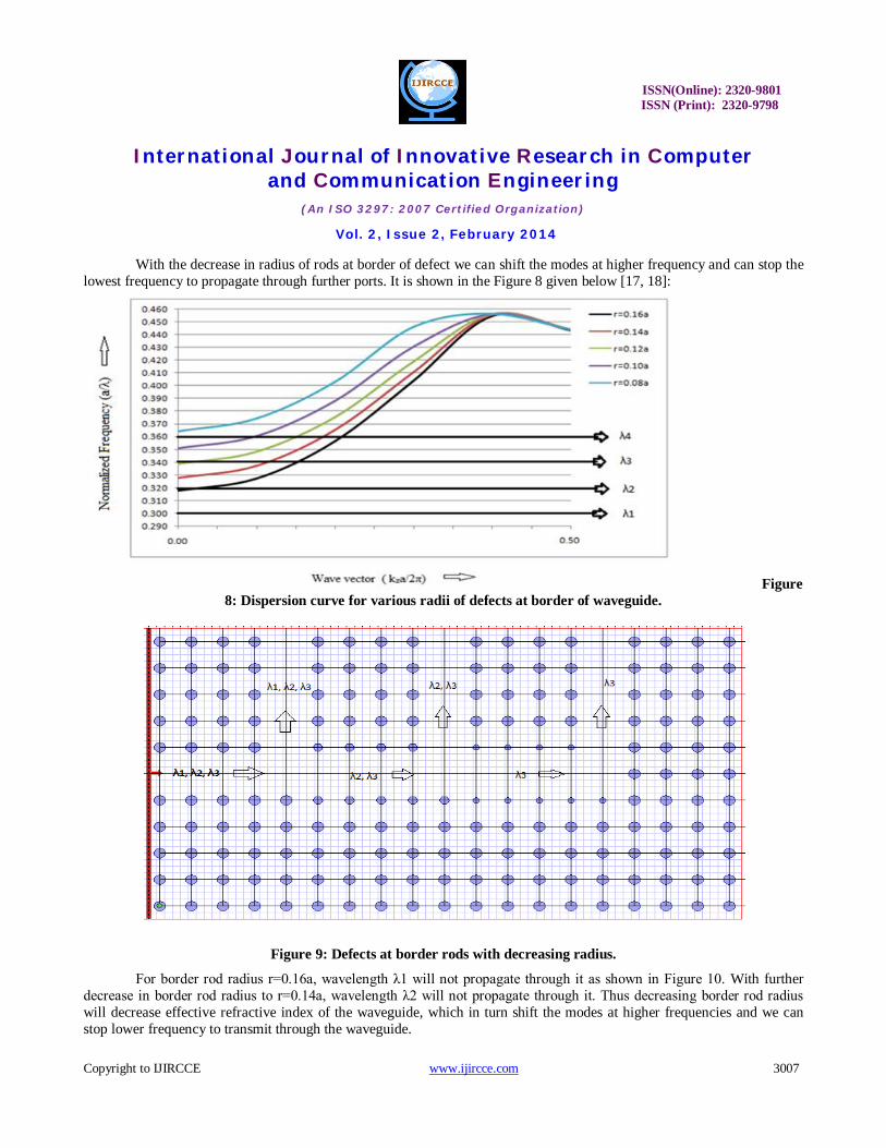
With the decrease in radius of rods at border of defect we can shift the modes at higher frequency and can stop the lowest frequency to propagate through further ports. It is shown in the Figure 8 given below [17, 18]:
Figure 8: Dispersion curve for various radii of defects at border of waveguide.
Figure 9: Defects at border rods with decreasing radius.
For border rod radius r=0.16a, wavelength λ1 will not propagate through it as shown in Figure 10. With further decrease in border rod radius to r=0.14a, wavelength λ2 will not propagate through it. Thus decreasing border rod radius will decrease effective refractive index of the waveguide, which in turn shift the modes at higher frequencies and we can stop lower frequency to transmit through the waveguide.

ISSN(Online): 2320-9801 ISSN (Print): 2320-9798
International Journal of Innovative Research in Computer and Communication Engineering
(An ISO 3297: 2007 Certified Organization)
Vol. 2, Issue 2, February 2014
Copyright to IJIRCCE www.ijircce.com 3008
Figure 10: Filter with specific wavelength at different output ports.
If we decrease the diameter of the border rods, the lower edge of the transmission band shifts to higher frequency as the amount of higher refractive index material is decreased in the waveguide. This effect can be used to prevent the propagation of a narrow wavelength range near the low-frequency transmission edge by decreasing the size of the border rods in consecutive sections along the photonic crystal waveguide. The restricted narrow wavelength band finds its guiding path along nearly placed waveguide and can be collected in that waveguide. Thus, a wavelength channel is demultiplexed to the adjacent photonic crystal waveguide from the incident signal. In this way we can design a multichannel optical demultiplexer by modifying border rods in consecutive sections which block some specific wavelength band and that can be collected at nearly placed waveguides. B. Design of de-multiplexer for three different optical windows wavelength We have proposed demultiplexer for wavelength corresponding to three different optical windows. Three wavelengths 1.31, 1.55 and 1.625μm are considered which correspond to second, third and fourth optical window respectively [19]. The proposed 2-D Photonic Crystal structure consists of square lattice with identical rods. The refractive index of rods is 3.47 (Si rods) and the radius of rods are taken as 0.18a (where ‘a’ is lattice constant).
It is seen from Figure 11 that photonic crystal with the radius of r = 0.18a has a band gap in frequency range (ω/2πc) = 0.573679 to 0.847886, 1.41463 to 1.457 for TE mode. Thus, if the lattice constant ‘a’ is taken as 0.52μm, the first PBG is at the normalized frequency range of 0.2983 ~ 0.4409(a/λ). For a=0.52μm, three wavelengths 1.31μm, 1.55μm and 1.625μm correspond to the normalized frequency 0.3969(a/λ), 0.3355(a/λ) and 0.32(a/λ) respectively, and as these frequencies lying in the PBG, thus cannot propagate through the photonic crystal until the defect is created in the structure. Three Gaussian input planes are used to launch the frequency corresponding to wavelength 1.31μm, 1.55μm and 1.625μm simultaneously at input port.
Radius of defect rod corresponding to output port 1, 2 and 3 are taken r1=0.07176μm (0.138a), r2=0.1872μm (0.36a), r3=0.13μm (0.25a) respectively. Demultiplexer is designed to receive wavelength 1.625μm, 1.55μm, 1.31μm at output port 1, 2 and 3 respectively. Radius of defect rods at output port 1 is taken after optimization of radius with the help of gap map diagram (Figure 1) and FDTD simulations such that it should propagate wavelength 1.625μm and prohibit the propagation of wavelength 1.55 and 1.31μm through it. Radius of the border rods of single line defect waveguide is

ISSN(Online): 2320-9801 ISSN (Print): 2320-9798
International Journal of Innovative Research in Computer and Communication Engineering
(An ISO 3297: 2007 Certified Organization)
Vol. 2, Issue 2, February 2014
Copyright to IJIRCCE www.ijircce.com 3009
decreased in section (black box) shown in the Figure 12 to prohibit transmission of wavelength 1.625μm from this section. Radius of border rods in black box section is taken as 0.0728μm (r=0.14a).
Figure 11: Band Gap for TE mode
Figure 12: De-multiplexer for wavelength 1.625μm, 1.55μm and 1.31μm

ISSN(Online): 2320-9801 ISSN (Print): 2320-9798
International Journal of Innovative Research in Computer and Communication Engineering
(An ISO 3297: 2007 Certified Organization)
Vol. 2, Issue 2, February 2014
Copyright to IJIRCCE www.ijircce.com 3010
Figure 13: Normalized Power measured at output port 1 (blue), output port 2 (red) and output port 3 (green).
Observation points (green dot) are placed at output port 1, 2 and 3 to observe the power received from the source. Power measured at output ports 1, 2 and 3 after simulation by Opti-FDTD (Finite differential time domain) is normalized with respect to the maximum power received at the corresponding port and is shown in Figure 13.
Quality factor Q=λ0/ΔλFWHM, with λ0 is the center wavelength and ΔλFWHM is the full wavelength width at half maximum, is the important parameter in wavelength division multiplexer which gives the resolution of wavelength selectivity. For wavelength selective applications high quality factor is required [20]. Table 1 gives the quality factor of every channel.
Channel λ0 (μm) Δλ (μm) Q 1 1.53 1.5269-1.533=0.0061 250.8196 2 1.55 1.5467-1.5528=0.0061 254.0983 3 1.57 1.5672-1.573=0.0058 270.6896
Table 1: Simulation results of wavelength division demultiplexer
Another important parameter in designing wavelength division demultiplexer is Crosstalk which is unwanted leakage or bleed of a signal from one or more channels to other channels within a device. Lower value of crosstalk is always desired [20, 21]. In Table 2 crosstalk is named as Xtij, which i and j vary from 1 to 3. Xtij shows the effect of crosstalk of output j in ith output ( i and j indices are row and column in Table 2 respectability). For example Xt12 shows the amount of crosstalk of Output 2 in Output 1.
Channel 1 (in dB) 2 (in dB) 3 (in dB) 1 ---- -10.46 -15.41 2 -6.48 ---- -9.813 3 -11.31 -9.65 ----
Table 2: Crosstalk amounts (Xtij) of the proposed structure (dB)
ISSN(Online): 2320-9801 ISSN (Print): 2320-9798
International Journal of Innovative Research in Computer and Communication Engineering
(An ISO 3297: 2007 Certified Organization)
Vol. 2, Issue 2, February 2014
Copyright to IJIRCCE www.ijircce.com 3011
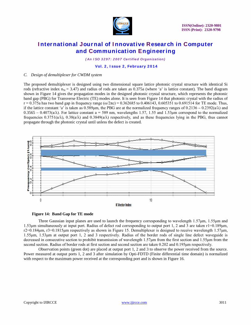
C. Design of demultiplexer for CWDM system The proposed demultiplexer is designed using two dimensional square lattice photonic crystal structure with identical Si rods (refractive index nSi = 3.47) and radius of rods are taken as 0.375a (where ‘a’ is lattice constant). The band diagram shown in Figure 14 gives the propagation modes in the designed photonic crystal structure, which represents the photonic band gap (PBG) for Transverse Electric (TE) modes alone. It is seen from Figure 14 that photonic crystal with the radius of r = 0.375a has two band gap in frequency range (ω/2πc) = 0.362685 to 0.406143, 0.605351 to 0.691514 for TE mode. Thus, if the lattice constant ‘a’ is taken as 0.589μm, the PBG are at the normalized frequency ranges of 0.2136 – 0.2392(a/λ) and 0.3565 – 0.4073(a/λ). For lattice constant a = 589 nm, wavelengths 1.57, 1.55 and 1.53μm correspond to the normalized frequencies 0.3751(a/λ), 0.38(a/λ) and 0.3849(a/λ) respectively, and as these frequencies lying in the PBG, thus cannot propagate through the photonic crystal until unless the defect is created.
Figure 14: Band Gap for TE mode
Three Gaussian input planes are used to launch the frequency corresponding to wavelength 1.57μm, 1.55μm and 1.53μm simultaneously at input port. Radius of defect rod corresponding to output port 1, 2 and 3 are taken r1=0.189μm, r2=0.184μm, r3=0.1815μm respectively as shown in Figure 15. Demultiplexer is designed to receive wavelength 1.57μm, 1.55μm, 1.53μm at output port 1, 2 and 3 respectively. Radius of the border rods of single line defect waveguide is decreased in consecutive section to prohibit transmission of wavelength 1.57μm from the first section and 1.55μm from the second section. Radius of border rods at first section and second section are taken 0.202 and 0.195μm respectively.
Observation points (green dot) are placed at output port 1, 2 and 3 to observe the power received from the source. Power measured at output ports 1, 2 and 3 after simulation by Opti-FDTD (Finite differential time domain) is normalized with respect to the maximum power received at the corresponding port and is shown in Figure 16.

ISSN(Online): 2320-9801 ISSN (Print): 2320-9798
International Journal of Innovative Research in Computer and Communication Engineering
(An ISO 3297: 2007 Certified Organization)
Vol. 2, Issue 2, February 2014
Copyright to IJIRCCE www.ijircce.com 3012
Figure 15: Demultiplexer for CWDM system
Figure 16: Normalized Power measured at output port 1 (blue), output port 2 (red) and output port 3 (green).
ISSN(Online): 2320-9801 ISSN (Print): 2320-9798
International Journal of Innovative Research in Computer and Communication Engineering
(An ISO 3297: 2007 Certified Organization)
Vol. 2, Issue 2, February 2014
Copyright to IJIRCCE www.ijircce.com 3013
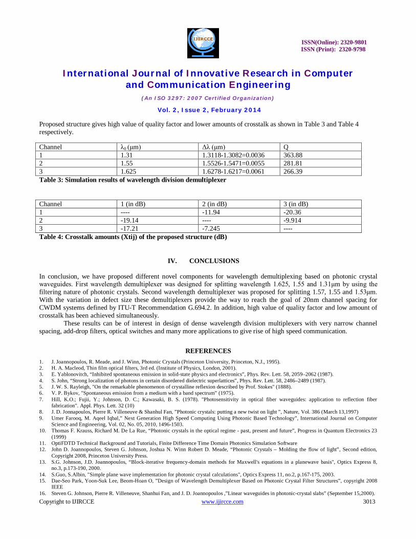
Proposed structure gives high value of quality factor and lower amounts of crosstalk as shown in Table 3 and Table 4 respectively.
Channel λ0 (μm) Δλ (μm) Q 1 1.31 1.3118-1.3082=0.0036 363.88 2 1.55 1.5526-1.5471=0.0055 281.81 3 1.625 1.6278-1.6217=0.0061 266.39 Table 3: Simulation results of wavelength division demultiplexer
Channel 1 (in dB) 2 (in dB) 3 (in dB) 1 ---- -11.94 -20.36 2 -19.14 ---- -9.914 3 -17.21 -7.245 ---- Table 4: Crosstalk amounts (Xtij) of the proposed structure (dB)
IV. CONCLUSIONS In conclusion, we have proposed different novel components for wavelength demultiplexing based on photonic crystal waveguides. First wavelength demultiplexer was designed for splitting wavelength 1.625, 1.55 and 1.31μm by using the filtering nature of photonic crystals. Second wavelength demultiplexer was proposed for splitting 1.57, 1.55 and 1.53μm. With the variation in defect size these demultiplexers provide the way to reach the goal of 20nm channel spacing for CWDM systems defined by ITU-T Recommendation G.694.2. In addition, high value of quality factor and low amount of crosstalk has been achieved simultaneously.
These results can be of interest in design of dense wavelength division multiplexers with very narrow channel spacing, add-drop filters, optical switches and many more applications to give rise of high speed communication.
REFERENCES 1. J. Joannopoulos, R. Meade, and J. Winn, Photonic Crystals (Princeton University, Princeton, N.J., 1995). 2. H. A. Macleod, Thin film optical filters, 3rd ed. (Institute of Physics, London, 2001). 3. E. Yablonovitch, “Inhibited spontaneous emission in solid-state physics and electronics”, Phys. Rev. Lett. 58, 2059–2062 (1987). 4. S. John, “Strong localization of photons in certain disordered dielectric superlattices”, Phys. Rev. Lett. 58, 2486–2489 (1987). 5. J. W. S. Rayleigh, "On the remarkable phenomenon of crystalline reflexion described by Prof. Stokes" (1888). 6. V. P. Bykov, "Spontaneous emission from a medium with a band spectrum” (1975). 7. Hill, K.O.; Fujii, Y.; Johnson, D. C.; Kawasaki, B. S. (1978). "Photosensitivity in optical fiber waveguides: application to reflection fiber
fabrication". Appl. Phys. Lett. 32 (10) 8. J. D. Jonnapoulos, Pierre R. Villeneuve & Shanhul Fan, ”Photonic crystals: putting a new twist on light ”, Nature, Vol. 386 (March 13,1997) 9. Umer Farooq, M. Aqeel Iqbal,” Next Generation High Speed Computing Using Photonic Based Technology”, International Journal on Computer
Science and Engineering, Vol. 02, No. 05, 2010, 1496-1503. 10. Thomas F. Krauss, Richard M. De La Rue, “Photonic crystals in the optical regime - past, present and future”, Progress in Quantum Electronics 23
(1999) 11. OptiFDTD Technical Background and Tutorials, Finite Difference Time Domain Photonics Simulation Software 12. John D. Joannopoulos, Steven G. Johnson, Joshua N. Winn Robert D. Meade, “Photonic Crystals – Molding the flow of light”, Second edition,
Copyright 2008, Princeton University Press. 13. S.G. Johnson, J.D. Joannopoulos, “Block-iterative frequency-domain methods for Maxwell's equations in a planewave basis", Optics Express 8,
no.3, p.173-190, 2000. 14. S.Guo, S.Albin, "Simple plane wave implementation for photonic crystal calculations", Optics Express 11, no.2, p.167-175, 2003. 15. Dae-Seo Park, Yoon-Suk Lee, Beom-Hoan O, ”Design of Wavelength Demultiplexer Based on Photonic Crystal Filter Structures”, copyright 2008
IEEE 16. Steven G. Johnson, Pierre R. Villeneuve, Shanhui Fan, and J. D. Joannopoulos ,”Linear waveguides in photonic-crystal slabs” (September 15,2000).

ISSN(Online): 2320-9801 ISSN (Print): 2320-9798
International Journal of Innovative Research in Computer and Communication Engineering
(An ISO 3297: 2007 Certified Organization)
Vol. 2, Issue 2, February 2014
Copyright to IJIRCCE www.ijircce.com 3014
17. Marko Loncar, Jelena Vuckovic and Axel Scherer,” Methods for controlling positions of guided modes of photonic-crystal waveguides” (September 2001).
18. Tapio Niemi, Lars Hagedorn Frandsen, Kristian Knak Hede,” Wavelength-Division Demultiplexing Using Photonic Crystal Waveguides”, IEEE PHOTONICS TECHNOLOGY LETTERS, VOL. 18, NO. 1, JANUARY 1, 2006.
19. Technical University of Lodz, Laboratory of Laser Molecular Spectroscopy, 93-590 Lodz, Wroblewskiego 15 str, Poland,” FUNDAMENTALS OF OPTICAL FIBER TRANSMISSION”.
20. A. Rostami, H. R. Habibiyan, F. Nazari, A. Bahrami and H. Alipour. A Novel Proposal for DWDM Demultiplexer Design Using resonance cavity in Photonic Crystal Structure. Asia Communications and Photonics (ACP) Conference, Shanghai 2009.
21. Kevin Lenglé, Mathilde Gay, Laurent Bramerie, Jean Claude Simon, Sylvain Combrié, Gaëlle Lehoucq, Alfredo de Rossi, Stefania Malaguti, Gaetano Bellanca, and Stefano Trillo,” Wavelength Division Demultiplexing and Crosstalk Assessment of a Photonic Crystal Filter”, IEEE PHOTONICS TECHNOLOGY LETTERS, VOL. 24, NO. 23, DECEMBER 1, 2012