vibrating mesh nebulizer reference...
TRANSCRIPT

AN2265Vibrating Mesh Nebulizer Reference Design
OVERVIEWIn medicine, a nebulizer is a drug delivery device thatbreaks up medical solutions into small aerosol droplets and deliver them directly to the patient’s airways for respiratory therapy. Medical nebulizers are commonly used for the treatment of COPD, asthma, cystic fibrosis and other respiratory diseases.
This application note demonstrates an implementation of driving a piezo mesh disk in a vibrating mesh nebu-lizer demo. The demo system features a Microchip 8-bit microcontroller-based piezo mesh disk driver board and a nebulizer plastic housing.
BASICS OF AEROSOL DRUG DELIVERYAccording to the American Association for Respiratory Care (AARC), the delivery of aerosolized medication directly to the airways is a mainstay in the emergency
treatment and long-term management of chronic obstructive pulmonary disease (COPD), asthma, and other chronic lung diseases in both the adult and pediatric populations.
It has several significant advantages over systemic drug delivery, including higher efficiency for selective treatment of pulmonary conditions, rapid treatment for bronchoconstriction, reduced incidence of side effects, and relative ease of self-administration by patients.
There are three common types of aerosol generators used for inhaled drug delivery:
• Small-volume nebulizer (SVN)
• Pressurized metered-dose inhaler (pMDI)
• Dry-powder inhaler (DPI)
In the SVN category, there are three main types of nebulizers:
• Pneumatic jet nebulizers
• Ultrasonic nebulizers
• Vibrating mesh nebulizers
FIGURE 1: BLOCK DIAGRAM FOR THE NEBULIZER DEMO
PIC16F1713
CLC
NCO
ADC
First Boost Stage (10‐20V)
Piezo Output Stage (30‐60V, 90‐150 KHz Sine Wave)
Piezo Mesh Disk
MCP2221USB‐to‐UART Converter
USB
CMP2
DAC1
CMP1
+
‐
‐
+
PWM3
PWM4
OPA2+
‐
3 Cell AAA Batteries
I/Os
EUSART
Button
LEDs
Output Current
Output Voltage
Boost Current
VDD
Boost Voltage
DAC2
Boost Gate
Output Frequency
OPA1+
‐
R
R R
R.
.
.
.
.
Authors: Bill HawkinsZhang FengMicrochip Technology Incorporated
2016-2017 Microchip Technology Inc. DS00002265B-page 1

VIBRATING MESH NEBULIZER REFERENCE DESIGN
VIBRATING MESH TECHNOLOGY
A significant innovation made in the nebulizer market is vibrating mesh technology. Basically, a vibrating mesh nebulizer is composed of a liquid reservoir with a piezo mesh disk mounted on one side of it, and a piezo mesh driver circuit board with batteries. The piezo mesh disk consists of a stainless steel plate that has been perfo-rated with thousands of precision-formed, laser-drilled holes, and surrounded by a piezoelectric material.
The piezoelectric material will vibrate at a very high rate of speed when it is driven by an analog signal of spe-cific voltage, frequency, and waveform that is gener-ated by the driver board. As a result of rapid vibration, solution is drawn through the holes to form droplets of consistent size that are delivered at a low velocity to be be inhaled directly into the lungs.
The vibrating mesh nebulizers offer many advantages when compared to other types of inhalers.
• Nebulize a variety of drugs
• Combine medications, as well as control dosage
• High efficiency with minimal residual medication volume
• Ease of use for all ages
• Portable, low-power, battery-operated
• Very quiet during operation
• Can be used at home, clinic, hospital or during travel.
NEBULIZER DEMO SYSTEM
The Microchip’s nebulizer demo system contains a PIC16F1713 8-bit microcontroller based piezo mesh disk driver board and a plastic housing for the nebu-lizer. The housing has a liquid reservoir and a piezo mesh element.
One of the challenges of designing a vibrating mesh nebulizer is to generate an adequate and reliable ana-log driving signal, as required to drive a corresponding piezo mesh disk. The piezo mesh disk requires a high voltage waveform at a specific resonant frequency.
The optimum frequency may vary device-to-device due to manufacturing tolerances. The following table shows typical characteristics:
TABLE 1: TYPICAL CHARACTERISTICS OF ANALOG DRIVING SIGNAL
Frequency 117 kHz ±5 kHz
Voltage 45Vp-p
Power <2W
The following sections of this application note describe how to use the rich peripherals of the PIC16F1713 MCU, and some discrete analog components to build a high performance, low power and low cost piezo mesh disk driver board. Use the following links to go to a spe-cific location in this application note.
Nebulizer Features
Boost Stage
Output Stage
Communications
Power
Nebulizer Software
Debug Warning
Detailed Software Operation
Initialization
Enabling/Disabling Output
State Machine
INIT State
SWEEP State
RUN State
STOP State
INDICATE State
SLEEP State
Interrupts
Circuit Description
Boost Circuitry
Output Circuitry
Summary
NEBULIZER FEATURES
Figure 1 shows a block diagram of the nebulizer demo. All of the logic and control is handled within the PIC16F1713 MCU. The power circuitry consists of two functions, a boost stage to generate a higher voltage from the batteries, and an output stage which produces the sine wave to drive the piezo mesh.
Figure 2 illustrates the principle of the vibrating mesh technology.
DS00002265B-page 2 2016-2017 Microchip Technology Inc.

VIBRATING MESH NEBULIZER REFERENCE DESIGN
FIGURE 2: VIBRATING MESH NEBULIZER
Vibrating Piezo Mesh Disk
Liquid is drawn through the holes to produce droplets of consistent size
Cross-section of a hole in the piezo mesh disk
The result is a fine-particle, low-velocity aerosol that is optimum for central and deep lung deposition.
Vibrating Piezo Mesh Disk Assembly
Reservoir of Medicated Solution
2016-2017 Microchip Technology Inc. DS00002265B-page 3
VIBRATING MESH NEBULIZER REFERENCE DESIGN
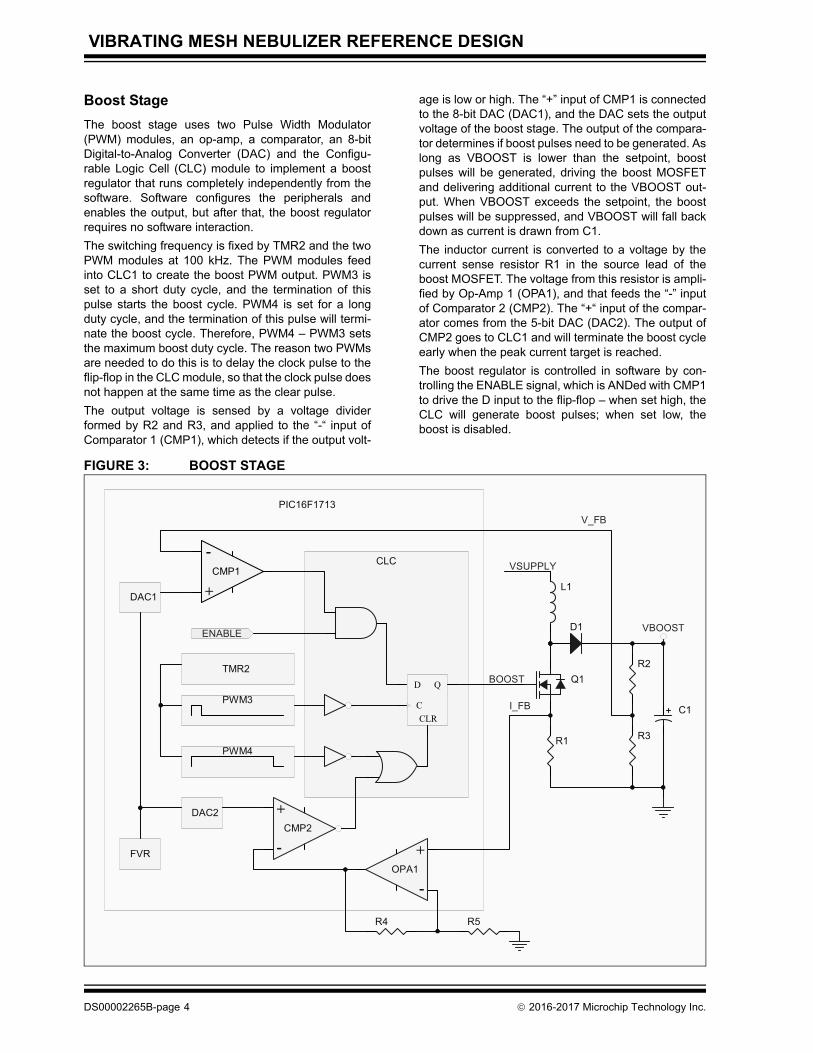
Boost Stage
The boost stage uses two Pulse Width Modulator (PWM) modules, an op-amp, a comparator, an 8-bit Digital-to-Analog Converter (DAC) and the Configu-rable Logic Cell (CLC) module to implement a boost regulator that runs completely independently from the software. Software configures the peripherals and enables the output, but after that, the boost regulator requires no software interaction.
The switching frequency is fixed by TMR2 and the two PWM modules at 100 kHz. The PWM modules feed into CLC1 to create the boost PWM output. PWM3 is set to a short duty cycle, and the termination of this pulse starts the boost cycle. PWM4 is set for a long duty cycle, and the termination of this pulse will termi-nate the boost cycle. Therefore, PWM4 – PWM3 sets the maximum boost duty cycle. The reason two PWMs are needed to do this is to delay the clock pulse to the flip-flop in the CLC module, so that the clock pulse does not happen at the same time as the clear pulse.
The output voltage is sensed by a voltage divider formed by R2 and R3, and applied to the “-“ input of Comparator 1 (CMP1), which detects if the output volt-
age is low or high. The “+” input of CMP1 is connected to the 8-bit DAC (DAC1), and the DAC sets the output voltage of the boost stage. The output of the compara-tor determines if boost pulses need to be generated. As long as VBOOST is lower than the setpoint, boost pulses will be generated, driving the boost MOSFET and delivering additional current to the VBOOST out-put. When VBOOST exceeds the setpoint, the boost pulses will be suppressed, and VBOOST will fall back down as current is drawn from C1.
The inductor current is converted to a voltage by the current sense resistor R1 in the source lead of the boost MOSFET. The voltage from this resistor is ampli-fied by Op-Amp 1 (OPA1), and that feeds the “-” input of Comparator 2 (CMP2). The “+“ input of the compar-ator comes from the 5-bit DAC (DAC2). The output of CMP2 goes to CLC1 and will terminate the boost cycle early when the peak current target is reached.
The boost regulator is controlled in software by con-trolling the ENABLE signal, which is ANDed with CMP1 to drive the D input to the flip-flop – when set high, the CLC will generate boost pulses; when set low, the boost is disabled.
FIGURE 3: BOOST STAGE
L1
R1
R2
R3
D1
C1
PIC16F1713
PWM4
DAC2
ENABLE
CLC
C
D Q
CLR
TMR2
FVR
+
-CMP1
+
-
CMP2
PWM3
VBOOST
BOOST
I_FB
V_FB
DAC1
+
-
OPA1
R4 R5
VSUPPLY
Q1
+
-
-
-
+
+
DS00002265B-page 4 2016-2017 Microchip Technology Inc.

VIBRATING MESH NEBULIZER REFERENCE DESIGN
Output Stage
The output stage provides the high-voltage sine wave drive signal for the piezo mesh disk. It is a boost topol-ogy as well, so it does provide gain over the bulk volt-age from the boost stage. The output MOSFET is driven by the Numerically Controlled Oscillator (NCO), which provides a variable frequency with a fixed 50% duty cycle. The fine adjustment range of the NCO allows the output stage to be tuned to the particular piezo device attached to the nebulizer.
Because the output stage is a boost topology, the piezo mesh disk can be driven both high and low with a single MOSFET. The MOSFET will pull the piezo low, and when MOSFET is turned OFF, inductor L2 becomes a current source that drives the piezo high. Inductor L3 converts what would be a sharp falling edge when the MOSFET turns ON into sine wave as it forms a reso-nant circuit with C4 and the piezo mesh disk. C3 is a DC blocking cap that keeps the voltage on the piezo symmetrical and prevents the DC voltage on VBOOST from affecting the piezo when you are not driving the output.
Additionally, there are circuits that monitor the current and peak voltage in the output stage and are used to determine the peak operating frequency to tune the output frequency to the piezo mesh disk.
FIGURE 4: OUTPUT STAGE
L2 L3
Q2
R6
C3
C4D2
R9
R10
R11
C5
PIEZO
VBOOST
PIC16F1713
NCO
+
-
OPA2
ADC
R7 R8
OUTPUT
VPK
IOUT+
-
2016-2017 Microchip Technology Inc. DS00002265B-page 5

VIBRATING MESH NEBULIZER REFERENCE DESIGN
Communications
A Windows GUI will be provided to monitor and control the nebulizer demo board. To allow the PIC16F1713 MCU to connect to a USB port on the PC, an MCP2221 USB-to-UART bridge chip is used with the serial port on the MCU.
Power
The nebulizer demo board can be powered by several power sources.
The board has clips to hold three AAA batteries. It can also be powered by the USB port. Jumper J1 selects between the two sources.
There is also a connector for an external power supply. This connector is in parallel with the batteries, so remove the batteries if you plan to use this input.
FIGURE 5: POWER SUPPLY CIRCUITRY
���
��
�������
����
��
��
��������������� ����
������������
���������
����� ����
There is a P-Channel MOSFET used for reverse polar-ity protection, since it is possible to insert the batteries backwards.
There is a second P-Channel MOSFET used to enable VSUPPLY, which provides power to the boost and out-put stages – since those are both boost topologies, there is no “off” state with those stages. This MOSFET allows the output to be disconnected from the power supply.
The PICkit 3 connector has a VDD connection, and can be used to power the PIC16F16F1713 MCU for soft-ware development that does not involve driving the piezo mesh disk. The circuitry to drive the disk requires more power than the PICkit 3 can source, so don’t attempt to drive the mesh without batteries or the USB connection. During development, it is a good idea to run from the USB power instead of batteries because the USB power is current limited, while the batteries have enough energy to damage the circuitry if not driven properly.
DS00002265B-page 6 2016-2017 Microchip Technology Inc.

VIBRATING MESH NEBULIZER REFERENCE DESIGN
Nebulizer Software
The nebulizer software uses several of the peripherals on the PIC16F1713 MCU. While you could go through the data sheet and write the code to initialize and con-trol these peripherals by reading the descriptions and register definitions, there is an easier way. The MPLAB® Code Configurator (MCC) allows you to select options and set up peripherals in a GUI environ-ment, and then it will generate the required code for the peripherals.
Refer to Appendix C: MCC Peripheral Setup for the MCC peripheral setup.
DEBUG WARNING
When debugging software, use the USB port or another current limited source to power the board. Since the boost and output stages free-run, there is no safe place in software where you can set a breakpoint and know that the outputs are off. If you run from bat-teries and the MCU stops with one of these MOSFETs On, then the batteries will provide enough current to damage the board.
The reason this is an issue is that the default action of MPLAB X IDE Integrated Development Environment is to freeze peripherals when the program hits a break-point or it is stopped in the debugger. When the periph-erals are frozen, the outputs lock in their current state. It is a good idea to go into the Project Properties and under the debugger options, uncheck the “Freeze Peripherals” box. If you do this, breakpoints will not be destructive, but the boost and output stages will con-tinue to run. If you are currently driving the piezo mesh disk when the breakpoint is hit, it will continue to run, and you will have to restart the code that is running to turn the output off.
FIGURE 6: DEBUG OPTIONS – FREEZE PERIPHERALS
2016-2017 Microchip Technology Inc. DS00002265B-page 7

VIBRATING MESH NEBULIZER REFERENCE DESIGN
DETAILED SOFTWARE OPERATION
Initialization
By using MCC, the initialization of the MCU is reduced to calling the function SYSTEM_Initialize(). This takes care of initializing all of the peripherals to the con-figurations defined in the MCC selections described In Appendix C: MCC Peripheral Setup. Then there are a few lines to put some application variables and flags into initial states.
Enabling/Disabling Output
When the system goes from inactive to active mode (or active to inactive mode), there are two outputs that must be controlled.
The first is the output of the CLC, which is used for the gate drive in the boost stage. Recall that the CLC is a D-Flip Flop that sets and clears the gate drive signal, based on PWM modules and Comparator 1, which monitors the switch current in the boost circuit.
There are multiple ways to control this output:
1. There is an enable signal for the CLC that could be manipulated.
2. The Peripheral Pin Select could be used to control the mapping of the signal to the output pin.
3. The PWM3 could be disabled or set to a 0x000 duty cycle.
However, a clean way to control that output is to control the value on the D input of the Flip Flop. This would make sure that there are no truncated cycles, and that shutdown and restart will keep the same timebase.
The D input comes from Gate 2 in the CLC. In the MCC setup, set Gate 2 with no inputs, so it is an OR gate with all inputs equal to 0. This means that the D input is also at 0, so when PWM3 clocks the Flip-Flop, the gate drive output stays low. To turn it on, connect the C1OUT signal to the D input of the Flip-Flop. Do this by setting the LC1D2G2T bit. To make this clean in the code, use a macro to implement the bit handling as shown in the following examples.
EXAMPLE 1:
To enable/disable the output stage, use the enable bit (N1EN) in the NCO1CON register. Again, use macros to make this clean in the code.
EXAMPLE 2:
#define BOOST_ON CLC1GLS1 = 8 // LC1D2G2T = 1#define BOOST_OFF CLC GLS1 = 0 // LC1D2G2T = 0
#define OUTPUT_ON NCO1CONbits.N1EN = 1#define OUTPUT_OFF CO1CONbits.N1EN = 0
DS00002265B-page 8 2016-2017 Microchip Technology Inc.

VIBRATING MESH NEBULIZER REFERENCE DESIGN
State Machine
The nebulizer demo software is implemented as a state machine. The state machine is easy to document and understand, and breaks the application down into smaller pieces that are easily coded. The limited inter-action between states also makes development and debugging simpler. Medical device software needs to go through verification and validation, and the correla-tion between the state machine documents and the software source code simplifies that process.
The nebulizer state machine uses the following states:
• INIT – sets up the I/O and peripherals to imple-ment the BOOST and OUTPUT stages
• SWEEP – determines the run frequency for the piezo mesh
• RUN – monitors the battery and pushbutton to determine when to shut down
• STOP – turns off the BOOST and OUTPUT stages, and puts the peripherals in a low power state
• INDICATE – shows on the LEDs why the device stopped
• SLEEP – sets the PIC16F1713 MCU to wake up on a button press, and enters sleep mode
Figure 7 shows the state machine diagram with the transitions between states.
FIGURE 7: STATE DIAGRAM
STOP
INIT
INDICATE
SLEEP
RUN
SWEEP
START
Flash TimerExpired
Button Press(Low Battery)
Button Press(Good Battery)
Output PowerReady
PeakDetected
Peak NotDetected
Button Press,Timeout, orLow Battery
2016-2017 Microchip Technology Inc. DS00002265B-page 9

VIBRATING MESH NEBULIZER REFERENCE DESIGN
Figure 8 shows a flowchart of the Nebulizer State Machine. This code is a loop that manages a timebase for the nebulizer, then executes the current state. If no valid state is determined, then it is forced into the STOP state.
FIGURE 8: NEBULIZER SOFTWARE FLOWCHART - STATE MACHINE
Start
Initialize ChipInitialize Application
State ==SWEEP?
Yes
Yes
Yes
Yes
Yes
No
No
No
No
No
Yes
No
State ==RUN?
State ==STOP?
State ==SLEEP?
State ==INIT?
To INIT State
FromINITState
ToSWEEP
State
FromSWEEP
State
To RUN State
FromRUNState
State ==INDICATE?
ToSTOPState
FromSTOPState
ToINDICATE
State
FromINDICATE
State
ToSLEEPState
FromSLEEPState
Maintain Timebase
Set Indication to None
State = STOP
DS00002265B-page 10 2016-2017 Microchip Technology Inc.

VIBRATING MESH NEBULIZER REFERENCE DESIGN
INIT State
Figure 9 shows a flowchart of the INIT state. This state starts up the BOOST stage and implements a delay to allow the boost voltage to ramp up and stabilize. After the BOOST is ready, the OUTPUT is enabled, and then the program advances to the SWEEP state.
FIGURE 9: NEBULIZER SOFTWARE FLOWCHART – INIT STATE
Enable FVR
Set Freq to Sweep Base Value
Enable BOOST
State = SWEEP
FromState
Machine
Returnto State Machine
Enable VSUPPLY
Setup Comparator DACs
Waiting for Boost Delay?
Boost Delay Finished?
Enable OUTPUT Set Boost Delay
Yes
Yes
No
No
Set Max Treatment Timer
2016-2017 Microchip Technology Inc. DS00002265B-page 11

VIBRATING MESH NEBULIZER REFERENCE DESIGN
SWEEP State
Coming out of the INIT state, the NCO is initialized to the lower limit of the frequency sweep. On each pass through the loop, the NCO Increment registers are set to the next value so that the frequency sweeps upward to the highest frequency.
FIGURE 10: NEBULIZER SOFTWARE FLOWCHART - SWEEP STATE
FromState
Machine
Returnto State Machine
IsFreq>Sweep
Hi Freq?
Read Output Current
Trend =Falling?
Current >Local Max Current?
Set Peak Detected
Current >Local Min Current?
Local Max = CurrentLocal Min = Current
Save Local Max and Freq
Local Min = Current Local Max = Current
PeakDetected?
Increase Freq by Step Size
Set Freq to Saved Value
State = RUN
Current <Local Max -
Offset?
Current >Local Min +
Offset?
Trend = RisingTrend = Falling
YesYes
Yes Yes
YesYes
Yes
No
No
No No
No No
No
Set Indication to Long Alternate Flash
State = STOP
DS00002265B-page 12 2016-2017 Microchip Technology Inc.

VIBRATING MESH NEBULIZER REFERENCE DESIGN
At each frequency, the output current is sampled. When the piezo mesh approaches resonance, the cur-rent will rise. If the piezo mesh is installed and operat-ing properly, a peak between the low and high frequencies of the SWEEP will be detected, and cur-rent will be lower on either side of that peak. The peak may not be the maximum point – the output current may actually be higher at the start or end of the SWEEP than the resonant frequency.
So, at every frequency in the SWEEP, sample the out-put current, and look at the history of the waveform. The value may either be decreasing or increasing. Look for the current to be decreasing, followed by an increasing period, and then another decreasing period. The frequency that gives the highest value during the increasing period is saved, then when the following decreasing period is detected, that frequency is logged as the maximum point. If the output current ramps up towards the end of the SWEEP, it will not be accepted as a new peak frequency, since a decreasing period will not be detected.
After the SWEEP completes, the frequency from the maximum point is loaded into the NCO and the SWEEP is terminated, and the output continues to run at that frequency until the nebulizer is turned off. For the pur-poses of the following graphs, the frequency sweeps through the entire range before committing to a run fre-quency, but it could just as easily start running as soon as the peak is detected.
The following graphs show the output current as the signal sweeps from 90 to 150 kHz. The TP7 signal on the bottom of the graph is high, between 100-150 kHz. The sweep between 90-100 kHz is not evaluated so that the output is stable and the feedback has settled before looking at the output current. This prevents any transients related to the BOOST or OUTPUT stages starting up from affecting the sweep evaluation.
Figure 11 shows the output current signal with a piezo mesh that operates at 117 kHz. You can see the peak of the piezo mesh is plainly visible, although the local maximum there is well below the final scan frequency.
FIGURE 11: OUTPUT CURRENT OVER FREQUENCY SWEEP – 117 KHZ PIEZO MESH
2016-2017 Microchip Technology Inc. DS00002265B-page 13

VIBRATING MESH NEBULIZER REFERENCE DESIGN
Figure 12 shows the same sweep with a piezo mesh that operates at 135 kHz. You can see the peak has moved, but it is still easily noticeable. In this case, there is a double peak. The frequency the algorithm locks onto will depend on how deep the dip is between the peaks, and whether one peak is higher than the other one. The piezo mesh manufacturer has designed the piezo to have this response to widen the acceptable operating frequency range. For that reason, it operates equally well at either of these frequencies, so which peak the software settles on does not really matter.
FIGURE 12: OUTPUT CURRENT OVER FREQUENCY SWEEP - 135 KHZ PIEZO MESH
DS00002265B-page 14 2016-2017 Microchip Technology Inc.
VIBRATING MESH NEBULIZER REFERENCE DESIGN
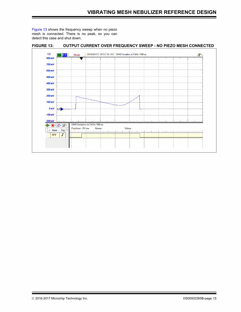
Figure 13 shows the frequency sweep when no piezo mesh is connected. There is no peak, so you can detect this case and shut down.
FIGURE 13: OUTPUT CURRENT OVER FREQUENCY SWEEP - NO PIEZO MESH CONNECTED
2016-2017 Microchip Technology Inc. DS00002265B-page 15

VIBRATING MESH NEBULIZER REFERENCE DESIGN
RUN State
While the nebulizer is in the RUN state, the system con-tinues operation at the same frequency setting. During this time, some conditions are monitored that might indicate a reason to shut down the nebulizer.
The following conditions are monitored:
1. Battery voltage – the battery is continually mon-itored during this time. The LED is updated, based on the battery voltage. A green LED indi-cates that the battery voltage is OK. When the voltage falls to a low battery level, the LED is turned to red. If the battery voltage continues to fall to the critical level, the system goes to the STOP State, then the INDICATE state flashes the red LED for 3 seconds to give the user suffi-cient time to see the indication and realize why the nebulizer was turned off.
2. Maximum treatment time counter – if the output is active for 10 minutes, the nebulizer is shut down automatically. This is to prevent continu-ous operation that would drain the batteries if the nebulizer is activated inadvertently, or the user walks away from it while it is running.
3. Button – the user can shut the nebulizer off at any time. The button is debounced, and the shutdown occurs when the button is released, so that it does not immediately start again when the user actually intends to turn it off.
DS00002265B-page 16 2016-2017 Microchip Technology Inc.

VIBRATING MESH NEBULIZER REFERENCE DESIGN
FIGURE 14: NEBULIZER SOFTWARE FLOWCHART - RUN STATEFromState
Machine
Returnto State Machine
Read Battery Voltage
Update Boost Duty Cycle by Battery
Voltage
Is Battery <3.5v?
Red LED OffGreen LED On
Red LED OnGreen LED Off
Is Button Pressed? Flag Button Press
Set 20ms Timer
Button Press Timer Expired?
Is Button Released?
Is Battery <2.9v?
MaxTreatment
TimerExpired?
Set Indication to None
Set Indication to Long Green Flash
Set Indication to Long Red Flash
State = STOP
Yes
Yes
Yes
Yes
Yes Yes
NoNo
No
No
No
No
FromState
Machine
Returnto State Machine
Read Battery Voltage
Update Boost Duty Cycle by Battery
Voltage
Is Battery <3.5v?
Red LED OffGreen LED On
Red LED OnGreen LED Off
Is Button Pressed? Flag Button Press
Set 20ms Timer
Button Press Timer Expired?
Is Button Released?
Is Battery <2.9v?
MaxTreatment
TimerExpired?
Set Indication to None
Set Indication to Long Green Flash
Set Indication to Long Red Flash
State = STOP
Yes
Yes
Yes
Yes
Yes Yes
NoNo
No
No
No
No
2016-2017 Microchip Technology Inc. DS00002265B-page 17

VIBRATING MESH NEBULIZER REFERENCE DESIGN
STOP State
When the nebulizer enters the STOP state, the supply voltage is shut off and the CLC and NCO outputs are driven low by using the macros described in Example 1 and Example 2. In preparation for low power sleep, the DACs and voltage reference (FVR) are turned off, and the program transitions to the INDICATE state.
FIGURE 15: NEBULIZER SOFTWARE FLOWCHART - STOP STATEFromState
Machine
Returnto State Machine
Disable BOOST
Disable OUTPUT
Disable VSUPPLY
Disable Comparator DACs
Disable FVR
State = INDICATE
FromState
Machine
Returnto State Machine
Disable BOOST
Disable OUTPUT
Disable VSUPPLY
Disable Comparator DACs
Disable FVR
State = INDICATE
DS00002265B-page 18 2016-2017 Microchip Technology Inc.
VIBRATING MESH NEBULIZER REFERENCE DESIGN
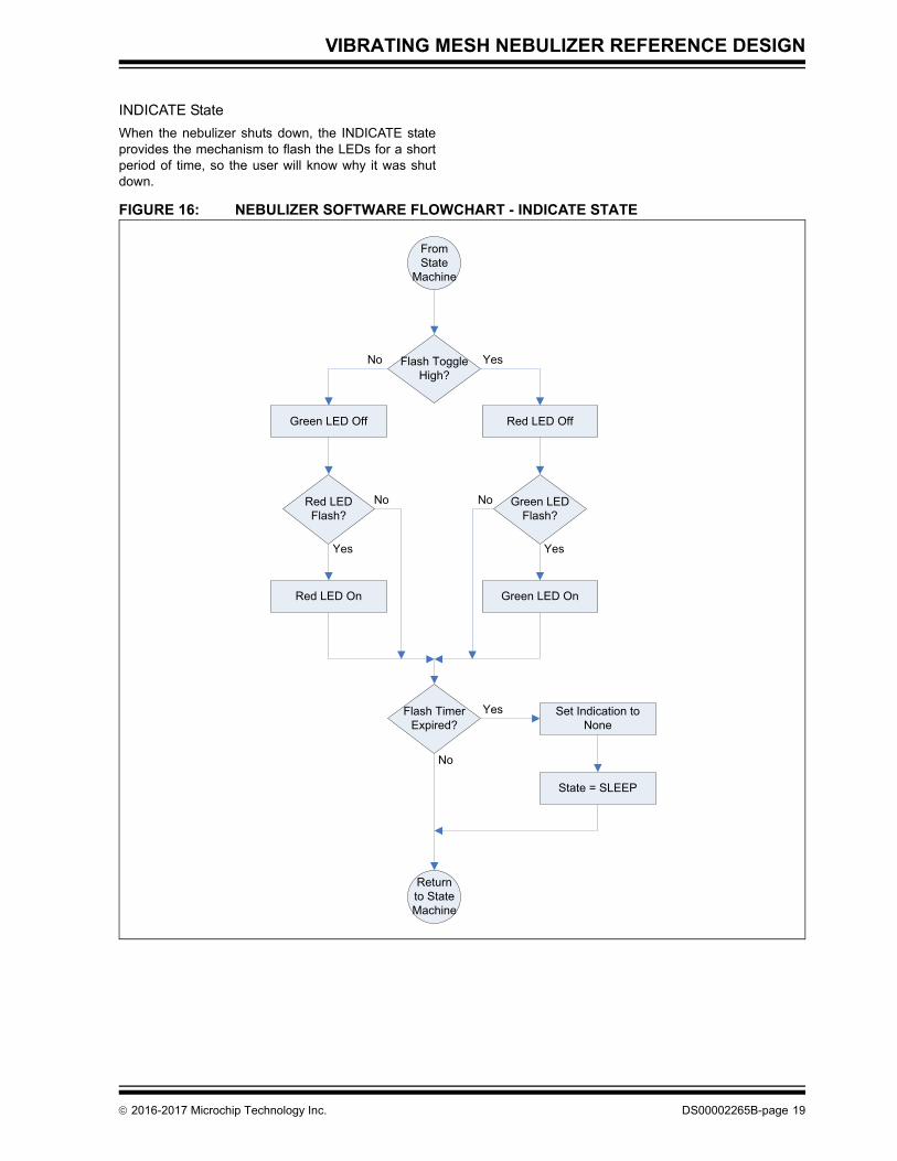
INDICATE State
When the nebulizer shuts down, the INDICATE state provides the mechanism to flash the LEDs for a short period of time, so the user will know why it was shut down.
FIGURE 16: NEBULIZER SOFTWARE FLOWCHART - INDICATE STATE
FromState
Machine
Returnto State Machine
Flash Toggle High?
Green LED Off Red LED Off
Red LED Flash?
Green LED Flash?
Green LED OnRed LED On
Flash Timer Expired?
Set Indication to None
State = SLEEP
Yes
YesYes
Yes
No
NoNo
No
2016-2017 Microchip Technology Inc. DS00002265B-page 19

VIBRATING MESH NEBULIZER REFERENCE DESIGN
SLEEP State
When the program enters the SLEEP state, it should already be in low power condition. The chip will be con-figured to wake on a button press, but if the button is still pressed, then that would present a problem. For this reason, there is a check to make sure that the but-ton is released first. If it is still pressed, the code will keep looping until the button is released, and then the MCU will be put in Sleep mode.
When the MCU wakes up, it is likely because of a but-ton press. But it is possible that some other event might have awakened the part.
To be sure, the button is tested – if it is not pressed, then the SLEEP state will be re-entered and the MCU will be put back into Sleep mode.
If the button is pressed, the program will wait for it to be released before proceeding. Then, the battery voltage is checked to make sure that it is in a valid range. If it is too low, the program goes to the INDICATE state and flashes the red LED. As long as the battery voltage is OK, the program transitions to the INIT state and the nebulizer starts up.
FIGURE 17: NEBULIZER SOFTWARE FLOWCHART - SLEEP STATE
FromState
Machine
Returnto State Machine
Set Chip to Wake Up on Button Press
Enter Sleep Mode
Is Button Pressed?
Is Button Released?
State = INIT State = INDICATE
Is Battery <2.9v?
Set Indication to Short Red Flash
Delay 20ms
Yes
Yes
Yes
No
No
No
Is Button Pressed?
Yes
No
DS00002265B-page 20 2016-2017 Microchip Technology Inc.

VIBRATING MESH NEBULIZER REFERENCE DESIGN
INTERRUPTS
The MCC has inserted interrupt routines to handle USART communications. These are the only interrupt routines that should get called. The Interrupt-On-Change that is used to wake the device from sleep should not go to the interrupt handler, because the chip is configured to simply wake up on the interrupt. How-ever, if the interrupt handler does get called as a result of Interrupt-On-Change, then the interrupt will continue to be re-entered unless there is code in the handler to clear the Interrupt-On-Change status. To address that possibility, a handler has been included that clears the interrupt condition.
2016-2017 Microchip Technology Inc. DS00002265B-page 21

VIBRATING MESH NEBULIZER REFERENCE DESIGN
Circuit Description
BOOST CIRCUITRY
Figure 18 shows the boost circuitry. Looking from VDD, there is a P-Channel MOSFET, Q1, that effectively dis-connects the power from the BOOST and OUTPUT stages. This is important because both stages are boost topology.
FIGURE 18: BOOST STAGE CIRCUITRY
���������
���
����������
��
���������
��
��� ���
���� ���!����
"#
$���%
$�%&! $
���
�������
��
���'(�
���� ��!
"�
���� ���!����
"�
�)*������%�����%�#
��
���� ������!
"�
���
$�%&+ $
��#�������
�#
$�%&��$
���� ����
"�
���
�����
�,� ������!
"�
��������
��
�
��
+�(�(������
�������
��
��,�����
�,
�������������
%�- $���%
%�-
!$���%
%�-
$�%&�.
%�-
$�%&! $
�, ������!
"��
���
��,�����
���
%�-
$�%&+ $
!��
A boost circuit will pass the input voltage straight through to the output, so the battery is constantly con-nected to the load if there is no switch to interrupt it. Q1 is driven directly from an output pin on the MCU, so before the BOOST stage is started, the BST_ENB out-put should be brought low. C1 and C2 provide a low impedance source for the BOOST stage to help com-pensate for Q1’s Rdson.
The BOOST stage is designed for a Vi from 2.9-5.5v, and a Vo of up to 20v at 100 kHz.
Q2 is the boost transistor. Since you want to run down to 2.9v, it is very important that this be a low gate threshold MOSFET. The gate voltage at 2.9v is not just 2.9v minus a voltage drop on the output pin – there is also a voltage drop caused by R9, the current sense resistor. This voltage drop further reduces the gate drive voltage, and if the Q2 is not chosen carefully, it will turn off when the inductor current starts ramping up. The transistor utilized here is RJP020N06 (ROHM Semiconductor), which has a max VGS threshold of 1.5v.
The BOOST stage works in hysteretic mode. When the boost voltage is lower than the threshold, gate pulses are generated for the BOOST stage.
When boost voltage rises above the threshold, no pulses are generated and the voltage decays as current is drawn from the output.
DS00002265B-page 22 2016-2017 Microchip Technology Inc.

VIBRATING MESH NEBULIZER REFERENCE DESIGN
The boost stage can work in the following modes:
• Continuous mode
• Discontinuous mode
If you design for maximum load, anything else will cause the BOOST stage to fall into Discontinuousmode, so it will probably operate in Discontinuousmode most of the time.
In Discontinuous mode, the inductor current falls to zero before the end of the switching cycle. Just think of it as a period that is longer than necessary. As the load current increases, the length of time the inductor cur-rent is zero decreases until it transitions to Continuousmode. At that point, the voltage gain is at its minimum and independent of load current; so, this is the limit of the Boost stage.
For Continuous mode, the duty cycle of a boost converter is given by:
D = 1 – (Vi/Vo)
For the boundary case of minimum Vi (2.9v) and maximum Vo (20v), this would give:
D = 1 – (2.9/20) = 0.855, or 85.5%
At maximum Vi (5.5v) this would give:
D = 1 – (5.5/20) = 0.725, or 72.5%
The software helps control peak current by adjusting the duty cycle to the Continuous mode duty cycle for the measured battery voltage and desired output volt-age. Pick an inductor value to keep it in Discontinuous mode, and then it will generate the boost voltage fast enough to skip cycles with the hysteretic controller. Additionally, the current limit will shut down the duty cycle early, if necessary, to prevent inductor saturation.
FIGURE 19: BOOST STAGE WAVEFORMS
2016-2017 Microchip Technology Inc. DS00002265B-page 23

VIBRATING MESH NEBULIZER REFERENCE DESIGN
OUTPUT CIRCUITRY
The output circuitry is essentially a series LC circuit,with a few special features. The piezo mesh assembly is the ultimate output element, and it is commonly capacitive. The particular piezo being targeted has a nominal resonant frequency of 117 kHz and a capaci-tance of 1.65 nF. Since it is off of the board and the rest of the circuit is a boost topology, there is also a capac-itor (C7) on the board, in parallel with the piezo. The capacitor is about 3x the value of the piezo so that the circuit operation is not significantly affected if the piezo mesh gets disconnected. C5 is a DC blocking capaci-tor, which needs to have a much greater value than the load of C7 and the piezo mesh so that it does not restrict the transfer of energy to the piezo mesh.
FIGURE 20: OUTPUT STAGE CIRCUITRY
+�(�(������%��
��
���������
���
��,�����
���
�� ������!
"��
������
�*%&+ $
���
����'(�
���� ���!����
"�
��, ���!����
",
���
��� ������
���
���������
��#
����������
���
�*%&! $
������
� ���!����
"��
���
��������
����'(�
�������������������������
�������
���
%�-
�/%&�.
%�-
���
%�- !*���
%�- �/%&+ $
����������
���
��
$�$0�'0�
��
���
*+�1�
��������������������
!$���%
DS00002265B-page 24 2016-2017 Microchip Technology Inc.

VIBRATING MESH NEBULIZER REFERENCE DESIGN
To get a good sine wave at the piezo, the resonant fre-quency of the LC circuit should be close to the physical resonant frequency of the piezo. The resonant frequency of an LC circuit is given by:
f = 1/(2 π)( √LC)
Solving for L, you get:
L = 1/(2 πf)2CL = 1/(2 π(117000Hz))2(4.7nF + 1.65nF) = 291µH
So, estimating 300 µH, divide that over L2 and L3 for 150 µH each. There will be some distortion in the wave-form since there are different inductances in the charge and discharge path, but it is a reasonable balance to drive the piezo with a single MOSFET and to boost the output voltage over VBOOST.
R18 measures the current in the output stage. As the circuit approaches resonance, the current will rise. Use this signal during the frequency sweep to detect the optimum output frequency, as described in the software section.
D2, R12, R13, R19 and C12 form a peak voltage detec-tor to monitor the output voltage at the piezo. (At the moment, this is being used for development purposes, it may not be necessary for production use.)
FIGURE 21: OUTPUT STAGE WAVEFORMS
2016-2017 Microchip Technology Inc. DS00002265B-page 25

VIBRATING MESH NEBULIZER REFERENCE DESIGN
SUMMARY
The vibrating mesh nebulizer is an aerosol drug deliv-ery device for respiratory therapy. It can be used by adults or children in the home, at a clinic or hospital, or during travel. This reference design is essentially aproduction-ready, single-chip solution that offers high performance, low-power and low-cost functionalities for the vibrating mesh nebulizer design.
REVISION HISTORY
Revision B (January 2017)
On page 5, two corrections were made in the second paragraph. C3 was replaced with C4, and C2 was replaced with C3.
DS00002265B-page 26 2016-2017 Microchip Technology Inc.

VIBRATING MESH NEBULIZER REFERENCE DESIGN
APPENDIX A: NEBULIZER DEMONSTRATION PICTURE
FIGURE 22: NEBULIZER EVALUATION BOARD
2016-2017 Microchip Technology Inc. DS00002265B-page 27

VIBRATING MESH NEBULIZER REFERENCE DESIGN
APPENDIX B: SCHEMATICSFIGURE 23: NEBULIZER EVALUATION BOARD SCHEMATICS
SMA
SS14
D1
IRLM
L010
0SO
T23Q
4
GN
D
221K
1% 0603
R5
15K
1% 0603
R8
GN
D
GN
D
2.2u
F10
0V12
06
C9
1.8
1206
1%R18
0.1u
F06
03
C11 G
ND
BST
_VFB
BO
OST
OPT
_IFB
BST
_VFB
GN
D
4.7K
0603
R16
10nF
0603
50V
C13
GN
DG
ND
OPT
_IFB
GN
D
150u
HL2
0.1u
F10
0V08
05
C5
4.7n
F20
0V08
05
C7
GN
D
GN
D
FREQ
100
0603
R4
270
0603
R17
270
0603
R20
22uH
L1
10uF
25V
C2
1 2 3 4 5 6
P1
0.1u
F10
0V08
05
C8
RJP
020N
06T1
00SO
T89
Q2
1500
pF06
0350
V
C6
GN
D
BST
_IFB
0.33
1206
1%R9
10 0603
R14
43
21
S1 SW T
act 6
x6
GN
D
0603
1AF1
GN
D
GN
D
RE3
/MC
LR/V
PP1
RA
0/A
N0/
C12
IN0-
/CLC
IN0
2R
A1/
AN
1/C
12IN
1-/O
PA1O
UT/
CLC
IN1
3
RA
2/A
N2/
C12
IN0+
/VR
EF-/D
AC
1OU
T14
RA
3/A
N3/
C1I
N1+
/VR
EF+
5
RA
4/O
PA1I
N+/
T0C
KI
6
RA
5/A
N4/
OPA
1IN
-/DA
C2O
UT1
/SS
7
VSS
8
RA
7/O
SC1/
CLK
IN9
RA
6/O
SC2/
CLK
OU
T10
RC
0/SO
SO/T
1CK
I/11
RC
1/SO
SI/C
CP2
12
RC
2/A
N14
/CC
P113
RC
3/A
N15
/SC
K/S
CL
14
RB
7/D
AC
12O
UT2
/CLC
IN3/
ICSP
DA
T28
RB
6/C
LCIN
2/IC
SPC
LK27
RB
5/A
N13
/T1G
26R
B4/
AN
1125
RB
3/A
N9/
C12
IN2-
/OPA
2IN
+24
RB
2/A
N8/
OPA
2IN
-23
RB
1/A
N10
/C12
IN3-
/OPA
2OU
T22
RB
0/A
N12
/C2I
N1+
/ZC
D/C
OG
1IN
/INT
21
VD
D20
VSS
19
RC
7/A
N19
/RX
/DT
18R
C6/
AN
18/T
X/C
K17
RC
5/A
N17
16R
C4/
AN
16/S
DI/S
DA
15
PIC
16F1
713-
I/SO
U1
47K
0603
R22
47K
0603
R24
MC
LR
PGC
PGD
MC
LR
PGC
PGD
BST
_IFB
BO
OST
OP2
OU
TO
P2-
FREQ
10K
1% 0603
R19
360K
1% 0603
R13
OPT
_VFB
OPT
_VFB
BST
_EN
B
(BST
_VLI
M)
0.1u
F06
03
C1
GN
D
ICSP
(BST
_ILI
M)
LED
_RED
LED
_GR
N
VD
D1
GP0
2
GP1
3
RST
4
UA
RT
RX
5
UA
RT
TX6
GP2
7G
P38
SDA
9SC
L10
VU
SB11
D-
12D
+13
VSS
14M
CP2
221
U2
0.1u
F06
03
C14
GN
DG
ND
0.1u
F06
03
C15
GN
D
USB
_TX
USB
_TX
USB
_RX
USB
_RX
USB
_RST
USB
_RST
USB
_SSP
ND
USB
_SSP
ND
USB
_CFG
USB
_CFG
USB
_D+
USB
_D+
USB
_D-
USB
_D-
0.1u
F06
0350
V
C4
GN
D
1500
pF06
0350
V
C16
GN
D
SWIT
CH
3x A
AA B
atte
ries
Batte
ry /
USB
Prog
/Deb
ug
Star
t/Sto
pU
ART/
USB
Brid
ge
Boos
t
Test
pnt
TP5
1K 0603
R6
10K
0603
R1
GN
D
OP2
-
OP2
OU
T
Op-
amp
Gai
n N
etwo
rks
Out
put C
urre
nt
Out
put
LED
_RED
LED
_GR
N
Test
pnt
TP7
1nF
100V
0805
C12
GN
D
1N41
48D
2
150u
HL3
Peak
Out
put V
olta
ge S
ense
0603
50V
DN
PC
3
0603
DN
PR
3
3
12
IRLM
L640
2Q
1
10K
0603
R2
4.7K
0603
R7
Out
put E
nabl
e
Powe
r-O
n Re
set
Test
pnt
BO
OST
Test
pnt
VB
OO
ST
Test
pnt
OU
T_SW
Test
pnt
FREQ
Test
pnt
GP1
Test
pnt
SCL
Test
pnt
GP3
Test
pnt
SDA
Test
pnt
GN
D1
Test
pnt
GN
D2
Test
pnt
BST
_SW
Test
pnt
BST
_VFB
Test
pnt
VPE
AK
Test
pnt
OU
T_IF
B
Test
pnt
OP2
OU
T
3
12
IRLM
L640
2Q
3
1K 0603
R10
GN
DRe
vers
e Po
larit
yPr
otec
tion
Sele
ctio
n
123
J3
ID4
VB
US
1
GN
D5
D-
2
D+
3
0
USB
2.0
MIN
I-B
FEM
ALE
J4
B3
AA
AB
2A
AA
B1
AA
A
110K
1% 0603
R12
2512
DN
PR
11 0603
100V
DN
PC
10
GN
D
47pF
0603
50V
C18
GN
D
Test
pnt
TP20
1 2
B2B
-EH
-A
J1
GN
D
PIEZ
O
DN
P
D3
4.7K
0603
R25
Test
pnt
BST
_IFB
Curr
ent V
olta
ge S
ense
12
TER
MIN
AL
1x2
J5G
ND
Exte
rnal
Pwr
4.7K
0603
R15
OP1
-
OP1
-
OP1
OU
T
OP1
OU
T
Test
pnt
OP1
OU
T
47K
0603
R23
GN
D47K
0603
R26
Boos
t Cur
rent
21 4
3
GR
EE
N
RE
D
RED
, GR
EEN
LD1
Test
pnt
GN
D3
DS00002265B-page 28 2016-2017 Microchip Technology Inc.

VIBRATING MESH NEBULIZER REFERENCE DESIGN
APPENDIX C: MCC PERIPHERAL SETUP
MCC is an MPLAB X IDE plug-in. It is downloaded when you get MPLAB X IDE, but it does need to be installed as a plug-in. For more details on MCC and installing it into MPLAB X IDE, click this link:
http://www.microchip.com/mcc
System
The first module in MCC to set up is the System mod-ule. This resource sets up the clock, and several other peripherals depend on the clock setting.
Figure 24 illustrates how to set up the clock to use the internal oscillator and to run at 16 MHz. The reason for setting the clock to this value is to get the best resolu-tion for the PWMs and NCO. Potentially, the clock speed could be reduced to save power and the resolu-tion in the PWMs and NCO may still be sufficient. But,the amount of power used by the MCU compared to the power used by the piezo mesh disk is very small, so theresulting power savings would be small, as well.
Configuration bits are also set up in this window by expanding the CONFIG1 and CONFIG2 entries. They are collapsed in this view just to save the space in the image, but you can look through the source code and see the settings there.
FIGURE 24: MCC SYSTEM SETTINGS
2016-2017 Microchip Technology Inc. DS00002265B-page 29

VIBRATING MESH NEBULIZER REFERENCE DESIGN
Timer0
Timer0 is used for timing for the LED and maximum treatment time. Set it up with a 1:256 prescaler and the internal timer, FOSC/4. Since you are running at 16 MHz, FOSC/4 is 4 MHz, and the prescaler reduces that down to 15.625 kHz. The timer is 8 bit, so a further reduction by 256 results in a frequency of 61 Hz (16.384 ms period).
FIGURE 25: TIMER0 SETTINGS
Timer2
Timer2 is the period timer for the PWM modules, so it should be set up before the PWMs. Since you want to run the Boost stage at about 100 kHz, set up Timer2 to overflow as close to 100 kHz as possible.100 kHz equals a period of 10 µs, so that is the target.
The first step is to click the Enable Timer box to tellMCC to start Timer2 after initialization. If you change the Prescaler setting, you can see the range for the Timer Period adjusts accordingly. At this point, type 10 µs into the Timer Period box. Then, when you click in any other box, MCC will show the value that is clos-est to what you specified. Since it can use 10 µsexactly, the value shows 10.0 µs for the Timer Period.
FIGURE 26: TIMER2 SETTINGS
DS00002265B-page 30 2016-2017 Microchip Technology Inc.

VIBRATING MESH NEBULIZER REFERENCE DESIGN
PWM
Next, set up PWM3 and PWM4, which are used for the BOOST stage.
For PWM3, start by checking the Enable PWM box. Choose Timer2 as the timer associated with this PWM. Set a fairly short period as the active period. PWM3 is essentially a forced dead time in the boost output.
It is important that there is enough time in this dead time to allow the current sense input to decay, and OPA1 and CMP1 to propagate that value through. Oth-erwise, the boost cycle may be terminated early from the current feedback of the last cycle. As a starting point, choose 10% here. Based on circuit performance you can increase or decrease this value.
FIGURE 27: PWM3 SETTINGS
PWM4 sets the maximum duty cycle for the boost stage. This should be set to a high value, but less than 100%. While running, this value may be updated by the software, based on the battery voltage, to pick an optimized duty cycle for the BOOST stage.
Click the Enable PWM box, and select Timer2 as the associated timer. Set the Duty Cycle to 99%, so that you have a high setting that is under 100%.
You may notice that both of the PWM modules are showing an error: “The PWM pin is not available.” This is because an output pin has not been assigned to these modules.
That is not a problem, because you are using these sig-nals internally as inputs to the CLC, so there is no rea-son to connect them to output pins. You can safely ignore this error.
FIGURE 28: PWM4 SETTINGS
2016-2017 Microchip Technology Inc. DS00002265B-page 31

VIBRATING MESH NEBULIZER REFERENCE DESIGN
FVR
The Fixed Voltage Reference (FVR) is used as a refer-ence for the DAC and the ADC modules. The MCU is powered directly from batteries, so VDD will vary as the batteries age. For this reason, using VDD as a refer-ence would not give the expected results.
The FVR buffers can multiply the 1.024v reference by 1, 2, or 3, giving 1.024v, 2.048v, or 4.096v. You want the nebulizer to operate down to a 2.9v input from the bat-teries (0.96v from each battery), so the 4.096v option is not achievable.
Therefore, choose 2x to feed the DAC and ADC with 2.048v, which should be stable across the entire VDD range from the batteries.
FIGURE 29: FVR SETTINGS
DS00002265B-page 32 2016-2017 Microchip Technology Inc.

VIBRATING MESH NEBULIZER REFERENCE DESIGN
DACs
DAC1 is used to set the output voltage limit for the BOOST stage. Use MCC to enable the DAC, set the positive reference to the FVR, and the negative reference to VSS.
Optionally, you can also enable the output of this volt-age on the DAC1OUT1 pin. This pin is available as a test point on the Nebulizer Evaluation Board.
FIGURE 30: DAC1 SETTINGS
DAC2 is used to set the current limit for the BOOSTstage. Enable the DAC with the FVR for the positive reference, and VSS for the negative reference.
FIGURE 31: DAC2 SETTINGS
2016-2017 Microchip Technology Inc. DS00002265B-page 33

VIBRATING MESH NEBULIZER REFERENCE DESIGN
Op-Amps
OPA1 is used to amplify the BOOST stage current sense. The current sense resistor needs to be very low resistance, because any voltage across this resistor subtracts from the gate drive voltage.
The amplified value from OPA1 gives more resolution for the comparator CMP2 to monitor peak current. Enable OPA1, select High Gain Bandwidth Power, OPA1IN, and leave Unity Gain Configuration unchecked, since the gain will be set by external resis-tors.
FIGURE 32: OPA1 SETTINGS
OPA2 is used to amplify the output stage current sense. Use MCC to enable OPA2, select the High Gain Band-width Power setting, and set the positive input MUX to use the OPA2IN+ pin.
Do not click the Unity Gain Configuration box, so that you can set the gain with resistor values.
FIGURE 33: OPA2 SETTINGS
DS00002265B-page 34 2016-2017 Microchip Technology Inc.

VIBRATING MESH NEBULIZER REFERENCE DESIGN
Comparators
CMP1 compares the VBoost output voltage to the reference voltage selected by DAC1.
The following options should be set for the comparator:
• click the box to enable the comparator
• enable the Zero Latency filter to prevent the com-parator output from oscillating
• set up the input MUXs to use the CIN1+ and CIN1- pins
FIGURE 34: CMP1 SETTINGS
CMP2 is used to check for the BOOST stage current hitting the target value, and terminating the duty cycle when that happens.
Click the boxes to enable the comparator and the Zero Latency filter. Set up the input MUXs to use the DAC2 and CIN0- pins, and set the output polarity to inverted.
FIGURE 35: CMP2 SETTINGS
2016-2017 Microchip Technology Inc. DS00002265B-page 35
VIBRATING MESH NEBULIZER REFERENCE DESIGN
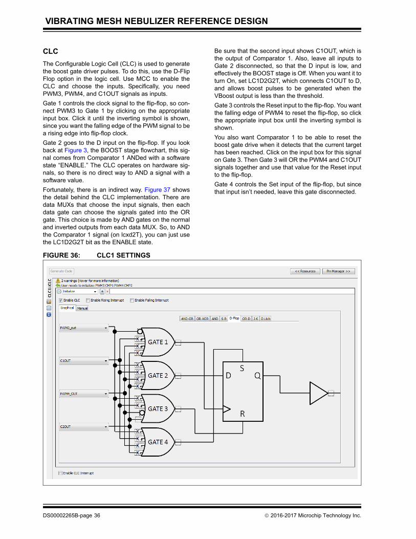
CLC
The Configurable Logic Cell (CLC) is used to generate the boost gate driver pulses. To do this, use the D-Flip Flop option in the logic cell. Use MCC to enable the CLC and choose the inputs. Specifically, you need PWM3, PWM4, and C1OUT signals as inputs.
Gate 1 controls the clock signal to the flip-flop, so con-nect PWM3 to Gate 1 by clicking on the appropriate input box. Click it until the inverting symbol is shown, since you want the falling edge of the PWM signal to be a rising edge into flip-flop clock.
Gate 2 goes to the D input on the flip-flop. If you look back at Figure 3, the BOOST stage flowchart, this sig-nal comes from Comparator 1 ANDed with a software state “ENABLE.” The CLC operates on hardware sig-nals, so there is no direct way to AND a signal with a software value.
Fortunately, there is an indirect way. Figure 37 shows the detail behind the CLC implementation. There are data MUXs that choose the input signals, then each data gate can choose the signals gated into the OR gate. This choice is made by AND gates on the normal and inverted outputs from each data MUX. So, to AND the Comparator 1 signal (on lcxd2T), you can just use the LC1D2G2T bit as the ENABLE state.
Be sure that the second input shows C1OUT, which is the output of Comparator 1. Also, leave all inputs to Gate 2 disconnected, so that the D input is low, and effectively the BOOST stage is Off. When you want it to turn On, set LC1D2G2T, which connects C1OUT to D, and allows boost pulses to be generated when the VBoost output is less than the threshold.
Gate 3 controls the Reset input to the flip-flop. You want the falling edge of PWM4 to reset the flip-flop, so click the appropriate input box until the inverting symbol is shown.
You also want Comparator 1 to be able to reset the boost gate drive when it detects that the current target has been reached. Click on the input box for this signal on Gate 3. Then Gate 3 will OR the PWM4 and C1OUT signals together and use that value for the Reset input to the flip-flop.
Gate 4 controls the Set input of the flip-flop, but since that input isn’t needed, leave this gate disconnected.
FIGURE 36: CLC1 SETTINGS
DS00002265B-page 36 2016-2017 Microchip Technology Inc.

VIBRATING MESH NEBULIZER REFERENCE DESIGN
FIGURE 37: CLC DETAILS
2016-2017 Microchip Technology Inc. DS00002265B-page 37

VIBRATING MESH NEBULIZER REFERENCE DESIGN
NCO
The NCO generates the output frequency for the piezo. Do not enable the NCO here, the software will enable and disable the NCO to turn the output drive on and off. Choose the HFINTOSC_16MHz option as the clock.source. That is the highest frequency clock available, and it will give the best resolution.
The piezo mesh assembly has a nominal operating fre-quency of 117 kHz. So, that is the value specified here for the NCO Output Frequency. However, this value gets overwritten in software during the frequency sweep. So, whatever you put here is actually irrelevant.
FIGURE 38: NCO1 SETTINGS
DS00002265B-page 38 2016-2017 Microchip Technology Inc.

VIBRATING MESH NEBULIZER REFERENCE DESIGN
ADC
The ADC is used to read the output current, output volt-age, and battery voltage. Enable the ADC, and set the clock that is used to determine the sampling rate. If you pick a value that results in a timing violation, it will show you an error here. The FOSC/16 is chosen here, which results in a sampling rate around 87 kHz.
Since the nebulizer circuitry operates directly from the battery, if the ADC reference is set to VDD, the value from the ADC will vary over the battery voltage range for the same voltage being read. This won’t show use-ful information, because it is difficult to know what the readings mean. To fix this, set the positive voltage to the FVR. Recall from the FVR setup that the ADC ref-erence value is 2.048v. The only precaution is to make sure that you do not have input voltages above that 2.048v level.
You can also use the pin manager tool to select inputs to read with the ADC. You can see here that RB4 is selected, which is the Output Voltage Feedback input. Click the Custom Name field if you want to change the name to something meaningful. Here, the signal has been renamed to OPT_VFB. This name will be used when setting up the ADC to read that value.
Notice that the Output Current Feedback input has not been added. This comes through OPA2, and because OPA2OUT is selected in the pin manager, MCC does not allow it to be chosen here for an ADC channel, as well. The MCU, however, can handle that configuration. So, that will have to set up in the software.
FIGURE 39: ADC1 INITIAL SETTINGS
2016-2017 Microchip Technology Inc. DS00002265B-page 39

VIBRATING MESH NEBULIZER REFERENCE DESIGN
For reading the battery voltage, a voltage divider on VDD could have been used to get the voltage under 2.048v. Then, another pin could have been used to read that through the ADC. But that would draw addi-tional current from the battery just to sense the voltage. There is an alternative.
Reconfigure the ADC to use VDD as the reference, then read the FVR, and use that value to calculate VDD. Remembering that the ADC produces a value based on the reference voltage:
Step = Reference/1023ADC = Vin / Step = Vin / (Reference/1023) = 1023 Vin / Reference
With VDD as the reference, Vin is the FVR, at 2.048v. That gives:
ADC = (1023 x 2.048v) / VDD
Since ADC is known, but VDD is not, solve for VDD:
VDD = (1023 x 2.048v) / ADC
You could reconfigure the ADC in software when you need to figure the battery voltage, but you can also use MCC and make an alternate configuration. Click the “+” next to the Initialize box, and a new configuration is cre-ated. Rename it “BatterySense”, then change the Positive Vref to VDD.
So, call ADC_BatterySense() before converting the battery voltage, and ADC_Initialize() before converting other ADC inputs.
FIGURE 40: AD1 BATTERY SETTINGS
DS00002265B-page 40 2016-2017 Microchip Technology Inc.
VIBRATING MESH NEBULIZER REFERENCE DESIGN
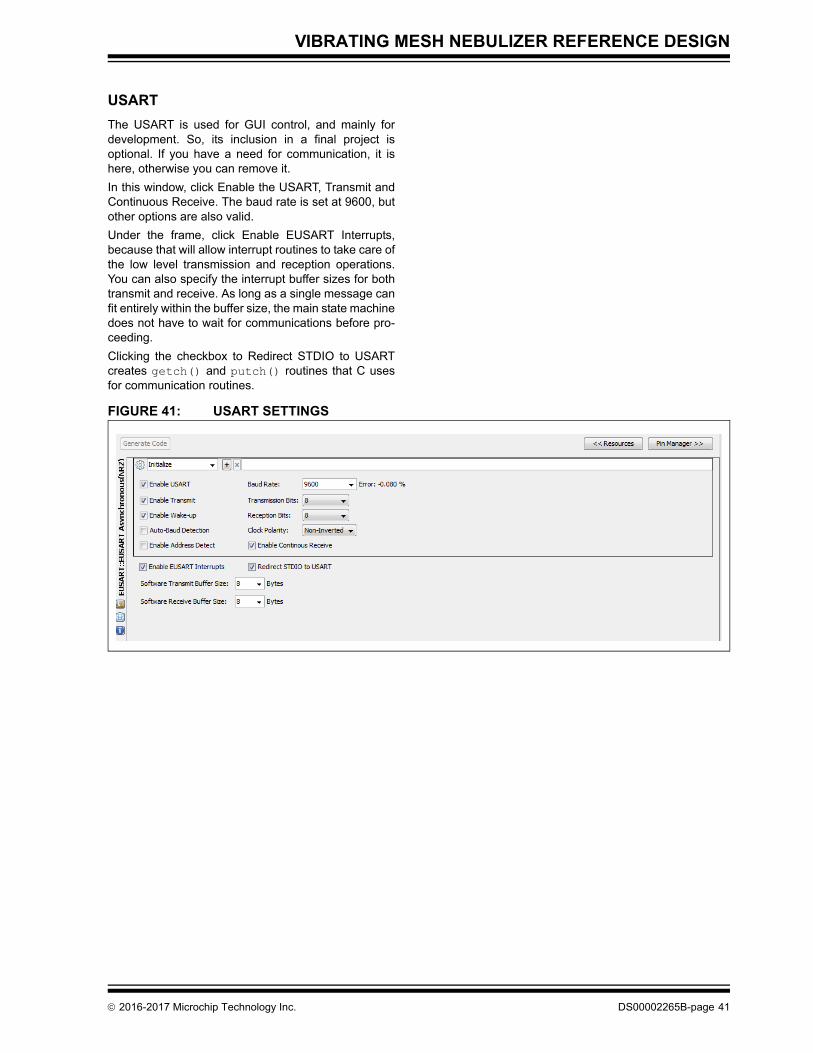
USART
The USART is used for GUI control, and mainly for development. So, its inclusion in a final project is optional. If you have a need for communication, it is here, otherwise you can remove it.
In this window, click Enable the USART, Transmit and Continuous Receive. The baud rate is set at 9600, but other options are also valid.
Under the frame, click Enable EUSART Interrupts, because that will allow interrupt routines to take care of the low level transmission and reception operations. You can also specify the interrupt buffer sizes for both transmit and receive. As long as a single message can fit entirely within the buffer size, the main state machine does not have to wait for communications before pro-ceeding.
Clicking the checkbox to Redirect STDIO to USART creates getch() and putch() routines that C uses for communication routines.
FIGURE 41: USART SETTINGS
2016-2017 Microchip Technology Inc. DS00002265B-page 41

VIBRATING MESH NEBULIZER REFERENCE DESIGN
Interrupt Manager
The interrupt manager is only used for USART commu-nications. You can change the order of the interrupts, but the USART handling is fast enough that it shouldnot make a difference, either way.
There is also a checkbox for Preemptive interrupt rou-tine. If it is checked, only one interrupt is serviced on each pass through the handler. If it is unchecked, then all interrupts active at the time the handler is called will be serviced before returning from the interrupt. Again, since the UART interrupt handler is very short, there will not be much of a difference, either way.
FIGURE 42: INTERRUPT MANAGER SETTINGS
DS00002265B-page 42 2016-2017 Microchip Technology Inc.

VIBRATING MESH NEBULIZER REFERENCE DESIGN
GPIO
The remaining pins are used for simple input or output. MCC allows you to select pins, give them a descriptive name, and set up available parameters for the pins – input/output, whether outputs start high or low, pull-ups for inputs, and Interrupt-On-Change settings.
FIGURE 43: GPIO SETTINGS
The pin manager shows a graphical representation of the chip and the pins assigned:
FIGURE 44: GRAPHICAL PIN MANAGER
2016-2017 Microchip Technology Inc. DS00002265B-page 43

VIBRATING MESH NEBULIZER REFERENCE DESIGN
APPENDIX D: LAYOUT
FIGURE 45: NEBULIZER EVAL BOARD LAYOUT – TOP LAYER
FIGURE 46: NEBULIZER EVAL BOARD LAYOUT – BOTTOM LAYER
DS00002265B-page 44 2016-2017 Microchip Technology Inc.

VIBRATING MESH NEBULIZER REFERENCE DESIGN
FIGURE 47: NEBULIZER EVAL BOARD LAYOUT – RENDERING
2016-2017 Microchip Technology Inc. DS00002265B-page 45

VIB
RA
TIN
G M
ES
H N
EB
UL
IZE
R R
EF
ER
EN
CE
DE
SIG
N
DS
00002265B
-page 46
2016-2017 M
icrochip Technolo
gy Inc.
Fo
otp
rin
t
Val
ue
Vo
lta
ge
2 AAA
0.1 µF 50V
10 µF 25V
DNP 50V
0.1 µF 100V
1500 pF 50V
4.7 nF 200V
2.2 µF 100V
DNP 100V
1 nF 100V
10 nF 50V
47 pF 50V
SS14 40V
1N4148
DNP
1A
ST_B2B-EH-A B2B-EH-A
HDR-2.54 Male 1x3
A_HIR_UX60-MB-5ST USB 2.0 MINI-B FEMALE
2_TH_RA_PHO_1725656 TERMINAL 1x2 63V
22µH
APPENDIX E: BILL OF MATERIALS (BOM)
The following table shows the BOM for the nebulizer evaluation board.
TABLE E: NEBULIZER EVALUATION BOARD BOM
Qu
anti
ty
Dig
ike
y®
De
sig
na
tor
Co
mm
en
t
De
scri
pti
on
6 BK-82-ND B1, B2, B3 AAA Battery Holder AAA BAT_HOLDER_AAA_BK-8
5 1276-1936-1-NDC1, C4,
C11, C14, C15
Cap - Ceramic Capacitor 1608[0603]
1 490-5523-1-ND C2 Cap - Electrolytic Polarized Capacitor (Radial) C0805
1 C3 Cap - Ceramic Capacitor 1608[0603]
2 1276-2923-1-ND C5, C8 Cap - Ceramic Capacitor 6-0805_L
2 1276-1960-1-ND C6, C16 Cap - Ceramic Capacitor 1608[0603]
1 399-11942-1-ND C7 Cap - Ceramic Capacitor 6-0805_L
1 490-7209-1-ND C9 Cap - Ceramic Capacitor C1206
1 C10 Cap - Ceramic Capacitor 1608[0603]
1 1276-1169-1-ND C12 Cap - Ceramic Capacitor 6-0805_L
1 1276-1009-1-ND C13 Cap - Ceramic Capacitor 1608[0603]
1 1276-2296-1-ND C18 Cap - Ceramic Capacitor 1608[0603]
1 SS14E-TPMSCT-ND D1 Schottky Schottky Diode SMA
1 1N4148WTPMSCT-ND D2 Diode Single SOD-123
1 D3 Diode Single SOD-123
1 0603SFV100F/32-2CT-ND F1 1A Fuse J1-0603
1 455-1611-ND J1 Header 1x2 HDR_M_2.5_1X2_S_TH_J
1 SAM1035-03-ND J3 Header 1x3 HDR_M_2.54_1x3
1 H2959CT-ND J4 CON USB 2.0 Mini_Micro Connector USB Mini CON_USB-B_Mini_SMD_R
1 277-1273-ND J5 Header 1x2 CON_TERMINAL_2.54_1x
1 SRN6045-220MCT-ND L1 Bourns, Inc. 33uH, 1.4A Inductor SRN6045

2016
-2017 Microchip T
echnology Inc.
DS
00002265B
-page 47
VIB
RA
TIN
G M
ES
H N
EB
UL
IZE
R R
EF
ER
EN
CE
DE
SIG
N
2 150 µH
1 RED, GREEN
1
2 IRLML6402
1 RJP020N06T100 60V
1 IRLML0100 100V
3 10K
1 DNP
1 100
1 221K
2 1K
4 4.7K
1 15K
1 0.33
1 DNP
1 110K
1 360K
1 10
2 270
1 1.8
4 47K
1 FSM4JSMA
1 PIC16F1713-I/SO
1 MCP2221
TA
Val
ue
Vo
ltag
e
SDR0603-151KLCT-ND L2, L3 Bourns, Inc. 150 µH, 320ma Inductor SRN6045
754-1093-1-ND LD1 LED DUAL 4 pin LED LED_DUAL_SMD_2x1.25 mm
952-2372-ND P1 Header 6 Header, 6-Pin HDR1X6
IRLML6402PBFCT-ND Q1, Q3 Transistor MOS-P GSD Transistor MOS SOT-23-3
RJP020N06T100CT-ND Q2 RJP020N06T100 N-Channel MOSFET SOT89N
IRLML0100TRPBFCT-ND Q4 IRLML0100 N-Channel MOSFET SOT-23_N_MAT
RMCF0603FT10K0CT-NDR1, R2,
R19Resistor Resistor J1-0603
R3 Resistor Resistor J1-0603
RMCF0603JT100RCT-ND R4 Resistor Resistor J1-0603
RMCF0603FT221KCT-ND R5 Resistor Resistor J1-0603
RMCF0603JT1K00CT-ND R6, R10 Resistor Resistor J1-0603
RMCF0603FT4K70CT-ND R7, R15, R16, R25 Resistor Resistor J1-0603
RMCF0603FT15K0CT-ND R8 Resistor Resistor J1-0603
A109657CT-ND R9 Resistor - 1/2W Resistor RESC1206(3216)_M
R11 Resistor Resistor - 3W RESC2512(6432)_M
RMCF0603FT110KCT-ND R12 Resistor Resistor J1-0603
RMCF0603FT360KCT-ND R13 Resistor Resistor J1-0603
RMCF0603JT10R0CT-ND R14 Resistor Resistor J1-0603
RMCF0603JT270RCT-ND R17, R20 Resistor Resistor J1-0603
RL16R1.8FCT-ND R18 Resistor - 1/2W Resistor RESC1206(3216)_M
RMCF0603FT47K0CT-ND R22,
R23, R24, R26
Resistor Resistor J1-0603
450-1129-ND *** S1 SW Tact 6x6Tactile Switch, SPST; Thru-Hole; Vertical
SW_PB_6x6 SM
PIC16F1713-I/SO-ND U1 PIC16(L)F1713_6 SOIC-28_SSOP-28_SPDIP-28 PIC16F1713 SOIC-28
MCP2221-I/ST-ND U2 MCP2221 SOIC-14_TSSOP-14_PDIP-14 TSSOP-14
BLE E: NEBULIZER EVALUATION BOARD BOM (CONTINUED)
Qu
anti
ty
Dig
ike
y®
De
sig
na
tor
Co
mm
en
t
De
sc
rip
tio
n
Fo
otp
rin
t

VIBRATING MESH NEBULIZER REFERENCE DESIGN
APPENDIX F: WARNINGS, RESTRICTIONS AND DISCLAIMER
This demo is intended solely for evaluation and devel-opment purposes. It is NOT intended for medical, diag-nostic or treatment use. Use of Microchip devices in life support and/or safety applications is entirely at the buyer's risk, and the buyer agrees to defend, indemnify and hold harmless Microchip from any and all dam-ages, claims, suits, or expenses resulting from such use.
APPENDIX G: REFERENCES
Microchip. PIC16(L)F1713/6 Cost Effective 8-Bit Intelligent Analog Flash Microcontrollers data sheet (DS40001726)
American Association for Respiratory Care.D. Gardenhire, A. Arzu, D. Hess, T. Myers. (2013)A Guide to Aerosol Delivery Devices for Respiratory Therapists, 3rd Edition.
DS00002265B-page 48 2016-2017 Microchip Technology Inc.

Note the following details of the code protection feature on Microchip devices:
• Microchip products meet the specification contained in their particular Microchip Data Sheet.
• Microchip believes that its family of products is one of the most secure families of its kind on the market today, when used in the intended manner and under normal conditions.
• There are dishonest and possibly illegal methods used to breach the code protection feature. All of these methods, to our knowledge, require using the Microchip products in a manner outside the operating specifications contained in Microchip’s Data Sheets. Most likely, the person doing so is engaged in theft of intellectual property.
• Microchip is willing to work with the customer who is concerned about the integrity of their code.
• Neither Microchip nor any other semiconductor manufacturer can guarantee the security of their code. Code protection does not mean that we are guaranteeing the product as “unbreakable.”
Code protection is constantly evolving. We at Microchip are committed to continuously improving the code protection features of our products. Attempts to break Microchip’s code protection feature may be a violation of the Digital Millennium Copyright Act. If such acts allow unauthorized access to your software or other copyrighted work, you may have a right to sue for relief under that Act.
Information contained in this publication regarding device applications and the like is provided only for your convenience and may be superseded by updates. It is your responsibility to ensure that your application meets with your specifications. MICROCHIP MAKES NO REPRESENTATIONS OR WARRANTIES OF ANY KIND WHETHER EXPRESS OR IMPLIED, WRITTEN OR ORAL, STATUTORY OR OTHERWISE, RELATED TO THE INFORMATION, INCLUDING BUT NOT LIMITED TO ITS CONDITION, QUALITY, PERFORMANCE, MERCHANTABILITY OR FITNESS FOR PURPOSE. Microchip disclaims all liability arising from this information and its use. Use of Microchip devices in life support and/or safety applications is entirely at the buyer’s risk, and the buyer agrees to defend, indemnify and hold harmless Microchip from any and all damages, claims, suits, or expenses resulting from such use. No licenses are conveyed, implicitly or otherwise, under any Microchip intellectual property rights unless otherwise stated.
2016-2017 Microchip Technology Inc.
Microchip received ISO/TS-16949:2009 certification for its worldwide headquarters, design and wafer fabrication facilities in Chandler and Tempe, Arizona; Gresham, Oregon and design centers in California and India. The Company’s quality system processes and procedures are for its PIC® MCUs and dsPIC® DSCs, KEELOQ® code hopping devices, Serial EEPROMs, microperipherals, nonvolatile memory and analog products. In addition, Microchip’s quality system for the design and manufacture of development systems is ISO 9001:2000 certified.
QUALITYMANAGEMENTSYSTEMCERTIFIEDBYDNV
== ISO/TS16949==
Trademarks
The Microchip name and logo, the Microchip logo, AnyRate, AVR, AVR logo, AVR Freaks, BeaconThings, BitCloud, CryptoMemory, CryptoRF, dsPIC, FlashFlex, flexPWR, Heldo, JukeBlox, KEELOQ, KEELOQ logo, Kleer, LANCheck, LINK MD, maXStylus, maXTouch, MediaLB, megaAVR, MOST, MOST logo, MPLAB, OptoLyzer, PIC, picoPower, PICSTART, PIC32 logo, Prochip Designer, QTouch, RightTouch, SAM-BA, SpyNIC, SST, SST Logo, SuperFlash, tinyAVR, UNI/O, and XMEGA are registered trademarks of Microchip Technology Incorporated in the U.S.A. and other countries.
ClockWorks, The Embedded Control Solutions Company, EtherSynch, Hyper Speed Control, HyperLight Load, IntelliMOS, mTouch, Precision Edge, and Quiet-Wire are registered trademarks of Microchip Technology Incorporated in the U.S.A.
Adjacent Key Suppression, AKS, Analog-for-the-Digital Age, Any Capacitor, AnyIn, AnyOut, BodyCom, chipKIT, chipKIT logo, CodeGuard, CryptoAuthentication, CryptoCompanion, CryptoController, dsPICDEM, dsPICDEM.net, Dynamic Average Matching, DAM, ECAN, EtherGREEN, In-Circuit Serial Programming, ICSP, Inter-Chip Connectivity, JitterBlocker, KleerNet, KleerNet logo, Mindi, MiWi, motorBench, MPASM, MPF, MPLAB Certified logo, MPLIB, MPLINK, MultiTRAK, NetDetach, Omniscient Code Generation, PICDEM, PICDEM.net, PICkit, PICtail, PureSilicon, QMatrix, RightTouch logo, REAL ICE, Ripple Blocker, SAM-ICE, Serial Quad I/O, SMART-I.S., SQI, SuperSwitcher, SuperSwitcher II, Total Endurance, TSHARC, USBCheck, VariSense, ViewSpan, WiperLock, Wireless DNA, and ZENA are trademarks of Microchip Technology Incorporated in the U.S.A. and other countries.
SQTP is a service mark of Microchip Technology Incorporated in the U.S.A.
Silicon Storage Technology is a registered trademark of Microchip Technology Inc. in other countries.
GestIC is a registered trademark of Microchip Technology Germany II GmbH & Co. KG, a subsidiary of Microchip Technology Inc., in other countries.
All other trademarks mentioned herein are property of their respective companies.
© 2016-2017, Microchip Technology Incorporated, All Rights Reserved.
ISBN: 978-1-5224-1295-3
DS00002265B-page 49

DS00002265B-page 50 2016-2017 Microchip Technology Inc.
AMERICASCorporate Office2355 West Chandler Blvd.Chandler, AZ 85224-6199Tel: 480-792-7200 Fax: 480-792-7277Technical Support: http://www.microchip.com/supportWeb Address: www.microchip.com
AtlantaDuluth, GA Tel: 678-957-9614 Fax: 678-957-1455
Austin, TXTel: 512-257-3370
BostonWestborough, MA Tel: 774-760-0087 Fax: 774-760-0088
ChicagoItasca, IL Tel: 630-285-0071 Fax: 630-285-0075
DallasAddison, TX Tel: 972-818-7423 Fax: 972-818-2924
DetroitNovi, MI Tel: 248-848-4000
Houston, TX Tel: 281-894-5983
IndianapolisNoblesville, IN Tel: 317-773-8323Fax: 317-773-5453Tel: 317-536-2380
Los AngelesMission Viejo, CA Tel: 949-462-9523Fax: 949-462-9608Tel: 951-273-7800
Raleigh, NC Tel: 919-844-7510
New York, NY Tel: 631-435-6000
San Jose, CA Tel: 408-735-9110Tel: 408-436-4270
Canada - TorontoTel: 905-695-1980 Fax: 905-695-2078
ASIA/PACIFICAsia Pacific OfficeSuites 3707-14, 37th FloorTower 6, The GatewayHarbour City, Kowloon
Hong KongTel: 852-2943-5100Fax: 852-2401-3431
Australia - SydneyTel: 61-2-9868-6733Fax: 61-2-9868-6755
China - BeijingTel: 86-10-8569-7000 Fax: 86-10-8528-2104
China - ChengduTel: 86-28-8665-5511Fax: 86-28-8665-7889
China - ChongqingTel: 86-23-8980-9588Fax: 86-23-8980-9500
China - DongguanTel: 86-769-8702-9880
China - GuangzhouTel: 86-20-8755-8029
China - HangzhouTel: 86-571-8792-8115 Fax: 86-571-8792-8116
China - Hong Kong SARTel: 852-2943-5100 Fax: 852-2401-3431
China - NanjingTel: 86-25-8473-2460Fax: 86-25-8473-2470
China - QingdaoTel: 86-532-8502-7355Fax: 86-532-8502-7205
China - ShanghaiTel: 86-21-3326-8000 Fax: 86-21-3326-8021
China - ShenyangTel: 86-24-2334-2829Fax: 86-24-2334-2393
China - ShenzhenTel: 86-755-8864-2200 Fax: 86-755-8203-1760
China - WuhanTel: 86-27-5980-5300Fax: 86-27-5980-5118
China - XianTel: 86-29-8833-7252Fax: 86-29-8833-7256
ASIA/PACIFICChina - XiamenTel: 86-592-2388138 Fax: 86-592-2388130
China - ZhuhaiTel: 86-756-3210040 Fax: 86-756-3210049
India - BangaloreTel: 91-80-3090-4444 Fax: 91-80-3090-4123
India - New DelhiTel: 91-11-4160-8631Fax: 91-11-4160-8632
India - PuneTel: 91-20-3019-1500
Japan - OsakaTel: 81-6-6152-7160 Fax: 81-6-6152-9310
Japan - TokyoTel: 81-3-6880- 3770 Fax: 81-3-6880-3771
Korea - DaeguTel: 82-53-744-4301Fax: 82-53-744-4302
Korea - SeoulTel: 82-2-554-7200Fax: 82-2-558-5932 or 82-2-558-5934
Malaysia - Kuala LumpurTel: 60-3-6201-9857Fax: 60-3-6201-9859
Malaysia - PenangTel: 60-4-227-8870Fax: 60-4-227-4068
Philippines - ManilaTel: 63-2-634-9065Fax: 63-2-634-9069
SingaporeTel: 65-6334-8870Fax: 65-6334-8850
Taiwan - Hsin ChuTel: 886-3-5778-366Fax: 886-3-5770-955
Taiwan - KaohsiungTel: 886-7-213-7830
Taiwan - TaipeiTel: 886-2-2508-8600 Fax: 886-2-2508-0102
Thailand - BangkokTel: 66-2-694-1351Fax: 66-2-694-1350
EUROPEAustria - WelsTel: 43-7242-2244-39Fax: 43-7242-2244-393
Denmark - CopenhagenTel: 45-4450-2828 Fax: 45-4485-2829
Finland - EspooTel: 358-9-4520-820
France - ParisTel: 33-1-69-53-63-20 Fax: 33-1-69-30-90-79
France - Saint CloudTel: 33-1-30-60-70-00
Germany - GarchingTel: 49-8931-9700Germany - HaanTel: 49-2129-3766400
Germany - HeilbronnTel: 49-7131-67-3636
Germany - KarlsruheTel: 49-721-625370
Germany - MunichTel: 49-89-627-144-0 Fax: 49-89-627-144-44
Germany - RosenheimTel: 49-8031-354-560
Israel - Ra’anana Tel: 972-9-744-7705
Italy - Milan Tel: 39-0331-742611 Fax: 39-0331-466781
Italy - PadovaTel: 39-049-7625286
Netherlands - DrunenTel: 31-416-690399 Fax: 31-416-690340
Norway - TrondheimTel: 47-7289-7561
Poland - WarsawTel: 48-22-3325737
Romania - BucharestTel: 40-21-407-87-50
Spain - MadridTel: 34-91-708-08-90Fax: 34-91-708-08-91
Sweden - GothenbergTel: 46-31-704-60-40
Sweden - StockholmTel: 46-8-5090-4654
UK - WokinghamTel: 44-118-921-5800Fax: 44-118-921-5820
Worldwide Sales and Service
11/07/16