vhdl expert system hardware synthesis
TRANSCRIPT

VLSI Design1994, Vol. 1, No. 2, pp. 113-126Reprints available directly from the publisherPhotocopying permitted by license only
(C) 1994 Gordon and Breach Science Publishers S.A.Printed in the United States of America
A VHDL Based Expert System for HardwareSynthesis
SAJJAN G. SHIVAComputer Science Department, University of Alabama in Huntsville, Huntsville, Alabama
JUDIT U. JONESRockwell International, 555 Discovery Drive, Huntsville, Alabama
(Received May 9, 1989, Revised October 16, 1989)
This paper describes an expert system for Hardware Synthesis. Details of the target digital system are input tothe expert system using Very High Speed Integrated Circuit Hardware Description Language (VHDL). TheVHDL representation is first translated to a knowledge representation scheme known as a ’hologram’ which is acombination of rule, frame and semantic network representation schemes. The hologram representation of thetarget system is then input to the inference engine, which matches the target system to the Knowledge Basecomponents and selects an appropriate set for implementation, and connects them creating a digital circuit. Somedesign examples are described. The expert system approach results in designs very close to designs from a humandesigner. In its present form, the system does not perform a design space exploration for alternate designs, butexpects the designer to alter the VHDL representation, after observing the results from previous design cycles.
Key Words: Expert system; Automatic synthesis; VHDL; Knowledge representation; Hardware synthesis
ue to the complexity of very large scale inte-grated circuits, the design phase of a new prod-
uct could take several years of work by design teams.Yet, the time from the conception of a new productto its appearance on the market has to be kept to aminimum to bring new products to market ahead ofcompetition. Design aids such as wire routers, com-puter aided design systems, simulation programs,and hardware synthesizers have been developed tomake the design time shorter. Overviews of hard-ware synthesis can be found in [1, 2].
In 1978 the Department of Defense initiated theVery High Speed Integrated Circuit (VHSIC) Pro-gram, to aid in the production of military integratedcircuits. VHDL was developed to help create an in-tegrated design environment, taking the designerthrough all phases of development, testing, and eval-uation. VHDL also facilitated the communication ofdesign requirements between the government andcontractors, since operations performed by an inte-
Send all Correspondence to: Dr. Sajjan G. Shiva, Computer Sci-ence Department, University of Alabama in Huntsville, Hunts-ville, Alabama 35899, (205) 895-6160
grated circuit (IC) could be described precisely inVHDL. VHDL became the U.S. Government stan-dard hardware description language in 1987 [3-5].
In hardware synthesis tools such as VHDL DesignSystem [6] by IBM and the MIMOLA synthesis sys-tem [7] with a VHDL front end tool [8], the highlevel behavioral VHDL description is first translatedinto a register transfer (RT) level representation,which is then translated into hardware.The IBM VHDL Design System is similar to the
VHDL design environment described in the nextSection. Before synthesis the VHDL structure is"flattened" by the Simplifier. The Synthesizer firstcreates a technology independent block structuredlogic model which is composed of latch elements,combinatorial elements and predefined components(given by component instantiations). Then the designis converted into a technology dependent logicmodel, which is used to create test patterns, place-ment, wiring, chip masks or printed circuit boards.The MIMOLA system was developed for the de-
sign of processors. The VHDL front end tool createsa process graph from the behavioral VHDL repre-sentation. This process graph is optimized using com-
113

114 SAJJAN G. SHIVA and JUDIT U. JONES
piler optimization techniques to parallelize sequen-tial representations. The VHDL front end tooldecomposes and optimizes (globally) the VHDL be-havioral representation and serves as an interfacebetween VHDL and the MIMOLA hardware de-scription language. The MIMOLA system developsthe hardware and the microcode, and performs de-sign analysis. The input to the synthesis system is aMIMOLA algorithm and a set of constraints. Thealgorithm and the constraints are user modifiable todevelop several versions of the hardware designed.The input is transformed into intermediate files, thenthe algorithmic programs are mapped to RT-behav-ior level programs. Up to three different versionscan be generated depending on variable bindings.This is followed by the decomposition of complexstatements with the help of some heuristics, with anattention paid to common subexpressions. This isfollowed by statement scheduling to maximize par-allelization (for microinstructions), register assign-ment, module selection (arithmetic modules), gen-erating interconnections and control.VHDL has also been utilized in the automated
design of control structures. The Control SynthesisSystem in [9] designs a Finite State Automaton Con-troller from a VHDL instruction set and a microar-chitecture. This controller is then translated into aphysical implementation by commercially availableCAD tools such as Datapath Compiler by VTItools.Research in the area of developing an expert sys-
tem which would function as a design tool in theVHDL design environment has been done at theUniversity of Alabama in Huntsville (UAH) byGreen [2, 10], Klon [11], and Jones [12]. Green de-signed the University of Alabama Hardware ExpertSynthesis System (UHESS) which serves as a designconsultant in the selection of VHSIC ICs. Klon in-vestigated the issues concerning interfacing UHESSto VHDL. He extended Green’s knowledge baserepresentation scheme to accommodate the moduleand signal concepts of VHDL and named it a hol-ogram. Jones extended the hologram representationand investigated the process of taking a completecircuit design from its VHDL representation and syn-thesizing it to a finished circuit design. A finishedcircuit design contains modules (which correspondto existing hardware functions) and their intercon-nections. This paper describes the current form ofthe hardware synthesizer.
OVERVIEW OF THE EXPERT SYSTEM
VHDLSOURCE
PROFILER I-
USER
VHDLSOURCE
ANALYZER
lASTAST [ DESIGN
LIBR/Y
1SIMULATOR
HARDWARESYNTHESIZER
OTHER TOOLS
FIGURE VHDL Design Environment.
library, the profiler, the simulator, and other designand analysis tools.To develop new hardware in the VHDL design
environment, first a VHDL source code descriptionis developed. The VHDL source code specifies theperformance requirements of the target hardwaresystem. It can be at one or more levels of a systemdesign hierarchy such as system level, componentlevel, logic level, gate level, or below. The VHDLanalyzer translates the source code into an inter-mediate form known as the abstract syntax tree(AST) which is incorporated into the design library.Based on user instructions, the profiler generates anAST representation which reflects the correct con-figuration (i.e., entities with the correct revisions areselected). The output of the profiler is incorporatedinto the design library and presented to the hardwaresynthesizer tool. The hardware synthesizer then pro-duces a circuit design.
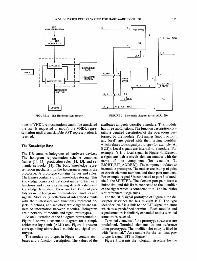
Figure 2 shows the block diagram of the hardwaresynthesizer. The hardware synthesizer has three ma-jor components: the AST to Inference Engine Input(IEI) translator, the inference engine and the knowl-edge base (KB). Top level details of these compo-nents are described in this section. Subsequent sec-tions will provide further details.
AST to IEI Translator
Figure 1 shows the VHDL design environment [13]consisting of the analyzer (a compiler), the design
The hardware synthesizer first translates the ASTrepresentation to the IEI representation. When por-
A VHDL BASED EXPERT SYSTEM FOR HARDWARE SYNTHESIS 115
USER
ASTREPRESENTATION
ASTto IEI
T,RANSLATOR
SYNTHESIZER
INFERENCEENGINE
KNOWLEDGEBASE
(HOLOGRAMLIBRARY)
S
COMP
A/8
SHIFTER
X2
CLK I 1
4
TWOSCOMP
4
2 X
,IICLK
4
Y/8 2
5 MA. MAX 1
-5 MA. MAX
8 C
EIGHT BITADDER
Xl
FIGURE 2 The Hardware Synthesizer. FIGURE 3 Schematic diagram for an ALU. [10]
tions of VHDL representations cannot be translatedthe user is requested to modify the VHDL repre-sentation until a translatable AST representation isreached.
The Knowledge Base
The KB contains holograms of hardware devices.The hologram representation scheme combinesframes [14, 15], production rules [14, 15], and se-mantic networks [14]. The basic knowledge repre-sentation mechanism in the hologram scheme is theprototype. A prototype contains frames and rules.The frames contain slots for knowledge storage. Thisknowledge consists of data pertaining to hardwarefunctions and rules establishing default values andknowledge heuristics. There are two kinds of pro-totypes in the hologram representation: modules andsignals. Modules (a collection of integrated circuitswith their interfaces and functions) represent ob-jects, functions, and activities; while Signals are car-riers of information between modules. Hologramsare a network of module and signal prototypes.As an illustration of the hologram representation,
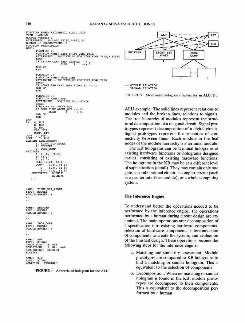
Figure 3 shows a schematic diagram for a simplearithmetic logic unit (ALU) and Figure 4 presentscorresponding abbreviated module and signal pro-totypes.The module prototypes in Figure 4 contain attri-
butes and a function description. The values of the
attributes uniquely describe a module. This modulehas three subfunctions. The function description con-tains a detailed description of the operations per-formed by the module. Port names (input, output,and local) are paired with their typing identifierwhich relates to its signal prototype (for example (A,BUS)). Local signals are internal to a module. Forexample, Y is a local signal in Figure 4. Elementassignments pair a circuit element number with thename of the component (for example (1,EIGHT_BIT_ADDER)). The component relates toits module prototype. The netlists are listings of pairsof circuit element numbers and their port numbers.For example, signal S is connected to port 3 of mod-ule 2, the SHIFTER. The element port pairs form a
linked list, and this list is connected to the identifierof the signal which is connected to it. The heuristicsslot references usage rules.For the BUS signal prototype of Figure 4 the de-
scriptor describes the bus as eight BIT. The typeidentifier itself is a link to the BIT signal structurewhich is a predefined terminal. Each module andsignal structure is similarly expanded until a terminalstructure is reached.
Terminal elements of the prototype structures arepredefined. Terminal elements do not referenceother prototypes. The modifier slot entry is filled inwith "terminal." An example for the terminal pro-totype is signal BIT in Figure 4.
Figure 5 presents the hologram structure for the
116 SAJJAN G. SHIVA and JUDIT U. JONES
FUNCTION NAME: ARITHMETIC LOGIC UNITTYPE MODULEMODULE NUMBER: 0ATTRIBUTES ALU,ADD,SHIFT,8-BIT,LSNUMBER OF SUBFUNCTIONS:FUNCTION DESCRIPTION:BEGIN
FUNCTION i:FUNCTION NAME: LEFT SHIFT ZERO FILLATTRIBUTES POSITIQE EN,OSITYVE EDGE TRIG,3 STATEBEGINIF (S AND CLK) THEN LSZF(A) --> C
ELSE --> CEND IFEND
FUNCTION 2:FUNCTION NAME: TWOS COMPATTRIBUTES POSITIVE EN,POSITIVE EDGE TRIGBEGINIF (COMP AND CLK) THEN TCOMP(B) --> YEND IFEND
FUNCTION 3:FUNCTION NAME: ADDATTRIBUTES POSITIVE EN,3 STATEBEGINADD(A,Y) --> ADDER OUTIF COMP THEN ADDER OUT --> C
ELSE --> CEND IFEND
ENDIN: A, BUS
B, BUSS, BITCLK, BITCOMP, BIT
OUT: C, BUSLOCAL: Y, BUSELEMENT ASSIGNMENTS:
i, EIGHT BIT ADDER2, SHIFTER3, TWOS COMP
NETLISTS:A; (i,i), (2,2)B; (3,2)S; (2,3)CLK; (2,1), (3,1)COMP; (1,4), (3,3)
c; (1,3), (2,4)Y; (1,2), (3,4)
HEURISTICS: RULE071RULE076
NAME: EIGHT BIT ADDERTYPE: MODULEMODULE NUMBER:
NAME: SHIFTERTYPE: MODULEMODULE NUMBER: 2
NAME: TWOS COMPTYPE: MODULEMODULE NUMBER:
NAME: BUSTYPE: SIGNALDESCRIPTOR: 8, BITCONDITIONS: 5, MA., MAXHEURISTICS: RULE062RULE065
NAME: BITTYPE: SIGNALMODIFIER: TERMINAL
FIGURE 4 Abbreviated hologram for the ALU
/" _-1"-- ----/’-5 ’USl/
SHZFTER EIGHT BIT TWOS
MODULE RELATIONSIGNAL RELATION
FIGURE 5 Abbreviated hologram structure for an ALU. [10]
ALU example. The solid lines represent relations tomodules and the broken lines, relations to signals.The tree hierarchy of modules represent the struc-tural decomposition of a diagonal circuit. Signal pro-totypes represent decomposition of a digital circuit.Signal prototypes represent the semantics of con-nectivity between them. Each module in the leafnodes of the module hierarchy is a terminal module.The KB holograms can be terminal holograms of
existing hardware functions or holograms designedearlier, consisting of existing hardware functions.The holograms in the KB may be at a different levelof sophistication (detail). They may contain only onegate, a combinational circuit, a complex circuit (suchas a printer interface module), or a whole computingsystem.
The Inference Engine
To understand better the operations needed to beperformed by the inference engine, the operationsperformed by a human during circuit design are ex-amined. The main operations are" decomposition ofa specification into existing hardware components,selection of hardware components, interconnectionof components to create the system, and evaluationof the finished design. These operations become thefollowing steps for the inference engine:
a. Matching and similarity assessment: Moduleprototypes are compared to KB holograms tofind a matching or similar hologram. This isequivalent to the selection of components.
b. Decomposition: When no matching or similarhologram is found in the KB, module proto-types are decomposed to their components.This is equivalent to the decomposition per-formed by a human.

A VHDL BASED EXPERT SYSTEM FOR HARDWARE SYNTHESIS 117
c. Name Unification: This process identifies cor-responding signal names in modules and se-lected KB holograms when the name and num-ber of ports do not match. This will help withthe connection of components when knowl-edge is necessary.
d. Evaluation of the design: The aggregate phys-ical properties of the system designed are com-puted and compared with the specification.This is equivalent to the evaluation performedby a human.
The inference engine has two major blocks: theanalyzer and the synthesizer.The analyzer decomposes the IEI, creating, as a
result, a tree hierarchy of modules which are alsoconnected by signals (i.e., the target hologram). Atthe leaf nodes of this tree, the modules are hologramsfound in the KB.Given the IEI, the analyzer begins to search the
KB for similar holograms. Attributes of the IEI mod-ule and the attributes of the root modules of KBholograms are compared, and similarity is evaluated.The outcome of this search could be: a matchinghologram found, a similar hologram found, or a sim-ilar hologram does not exist. In each case the actionsto be taken are as follows:
a. When a matching hologram is found, its prop-erties will be copied into the module aftersome name unifications. If the matching KBhologram has submodules, its subtree is cop-ied also into the module.
b. When a similar hologram is found, the defi-ciencies of the selected hologram will be ana-lyzed, corrected if possible, and components(submodules) are generated (i.e., the moduleis decomposed). Correcting the deficiencies isattempted by using heuristics. For example ifthe selected module has less BITs than theBIT-attribute indicates, then submodules aregenerated which collectively have at least asmany BITs as are needed. If correcting thedeficiencies is not possible, then the hologramwill be rejected, and the case of no similarhologram will be considered.
c. When a similar hologram does not exist, themodule is decomposed to its submodules, ifthe function description of the IEI module hascomponents. If the decomposition is not pos-sible, then the help of the designer is re-quested.
The details of the similarity evaluation process areprovided in the section (Similarity Assessment).
When the module is decomposed, each newly createdsubmodule is subject to the above process. This pro-cess could yield new submodules, which are in turnsubjected to the procedure described above. Thisprocess will continue until all submodules generatedare processed, and each leaf node corresponds to amatching KB hologram. The phase just described isthe requirement decomposition phase.The synthesizer evaluates the new design, based
on the physical properties of the terminal holograms.Here, physical properties of children nodes are syn-thesized to become the physical parameters of theparent node. This process begins at the leaf nodesand propagates actual design constraints upward inthe tree until the root module of the target hologramis reached. These actual design constraints refer topropagation delays, power supply requirements,compatibility of signal drivers and receivers, etc. Thephysical properties of the new design are comparedto the requirements contained in the IEI .module.The difficulty lies in the fact that the design uses
nonmonotonic reasoning. The correctness of designassumptions can be verified only by exploring all con-sequences of assumptions. Assumptions are the at-tribute evaluating KB heuristics, and heuristics whichdetermine what action to take to improve similarity.The incorrect assumptions must be pinpointed andother design assumptions substituted. If the new de-sign does not meet all the requirements of the IEImodule, additional requirements are given by theuser (by altering the VHDL representation), and thedesign process is repeated. This phase of the designmay be aided by a design tool facilitating overallsystem planning described in [16].
KNOWLEDGE REPRESENTATION
In this section first the reasons for the selection ofthe knowledge representation scheme are given, fol-lowed by the detailed description of the knowledgerepresentation.Three popular knowledge representation schemes
are: production rules, frames and semantic nets.For the representation of modules and signals pro-
duction rules alone are not suited to represent het-erogeneous knowledge grouped together. The prob-lem is the awkward acquisition of knowledgepertaining to a particular device, since productionrules are unordered. Frames are good devices togroup together heterogeneous knowledge, but theycan not easily express special knowledge about theuse of the frame. The prototype representation com-bines the advantages of both these representations.

118 SAJJAN G. SHIVA and JUDIT U. JONES
Comparison of two semantic nets is slow, since thewhole network has to be traversed. But new mean-ings are easily created. Pure prototype representa-tion does not facilitate the easy creation of newmeanings; but comparison is easy, since only the rootmodules and signals need to be compared.The hologram representation used by the synthesis
system holds advantages over pure prototype or puresemantic network representation and provides mech-anisms for both the dynamic creation of new mean-ings and easy comparison.The attributes of the module prototypes represent
the properties of objects in a very compact form.During similarity assessment, attributes of the rootmodule of KB holograms or the absence of attributesis evaluated according to heuristic rules. The use ofattributes is beneficial because of three reasons.First, KB search would take a considerable amountof time if each field of the root modules of KB hol-ograms were compared to each field of a module (tobe matched) when a similar hologram is searchedfor. Comparing and evaluating only the attributes ofthese objects speeds up the similarity assessment pro-cess. Second, differences between KB holograms anda module are efficiently determined by the sum ofthe attribute differences. Without the attributes, ana-lyzing the differences would take considerable searchtime, knowledge, and storage requirement. Third,optimization for different design options is facilitatedby the use of attributes.There are several requirements for which a digital
design could be optimized. For example: number ofcomponents, cost, speed, size, heat generated, longlife, mass production, etc. To optimize a design toany of these requirements or any combination ofthem requires a different approach. Accommodatingdifferent design criteria is facilitated with the use ofattributes, since only the attribute evaluation heu-ristics need to be changed. The drawbacks of the useof attributes are that they have to be derived fromthe VHDL representation, and they require storage.For easy automatic decomposition and name uni-
fication, the function description of module proto-types should be in a special form. This special formshould allow: (a) decomposition, (b) name unifica-tion, and (c) should contain knowledge of existingcomponents.To develop this special function description, con-
sider the functioning of a digital circuit. Here, theinputs are transformed to intermediate signals by afunction and these intermediate signals are trans-formed to the next level of intermediate signals byanother function, and so on until the output signalsare generated. Consider the analogy between these
functions and primitives of a language. Then a lan-guage comes to mind whose primitives are the func-tions of actual hardware devices, the Actual DevicePrimitives (ADPs). The ADPs are statements in theActual Device Language (ADL). If the function de-scription of a module can be expressed in this lan-guage, the hardware design is done in theory (at ahigh level), because it does not take into consider-ation lower level design constraints (such as propa-gation delay, power supply requirements, etc.). Eachleaf node in the design tree is an ADP, and eachintermediate node is an aggregate of ADPs havingas many subfunctions as there are submodules.Therefore, each function definition at a higher levelis expressed as a number of subfunctions where thesubfunctions have subfunctions and so on. ADP ex-amples are described in the section (The Actual De-vice Language).With the use of ADL in the decomposition or anal-
ysis phase, when no matching (or similar) hologramis found in the KB, the module is simply decomposedsuch that for each subfunction a submodule is allo-cated. From the function description allocated tosubmodules, and from the input and output signalsof a module, the input and output signals of thesubmodules can be determined. The local signals ofthe module are derived also from the same data. Theinteractions between the allocated submodules arespecified by the local signals. The allocated sub-modules then become independent modules and allsignals connected to them including local signals areconsidered as inputs or outputs.With the use of ADL, name unification can also
be accomplished. For name unification, there needsto be a way to identify which names correspond toeach other in the root module of a KB hologram anda module. Simple positional correspondence couldbe used in port lists (if there is a convention for portordering) if the number of ports and their functionsmatch. The situation here could be different when asimilar KB hologram is selected, since the numberof ports and/or their functions may not match. Sinceeach module has a function description generatedfrom ADPs, the two functions can be compared andnames falling in the same position textually unified.Therefore, a priori knowledge of the signals belong-ing to a hologram finally selected are not necessary.For automatic hardware synthesis, two approaches
could be used. One is that the hardware synthesizerdevelops all alternatives with a nondeterministic de-sign approach; the other is that the hardware device(HD) constraints are taken into consideration earlyon in the design. Here HD stands for existing hard-ware functions. It is easily seen that the nondeter-

A VHDL BASED EXPERT SYSTEM FOR HARDWARE SYNTHESIS 119
ministic design approach would take many iterations,and it would provide design alternatives, many ofwhich are not realizable or are very inefficient. Withthe use of ADL, the nondeterministic design ap-proach is avoided. Therefore, the second approachmust be used; some HD constraints have to be takeninto consideration at the design specification (VHDLcode generation) phase. To enforce these con-straints, VHDL representations of non-existing HDsare discovered at the VHDL to ADL translation pro-cess. These non-existing HDs then are modified bythe designer. This is equivalent to the idea that thepurely top down design methodology can not beused, since this would be the nondeterministic ap-proach. A combination of top down and bottom upmethodologies is needed.ADL saves time, since effort is not expended on
the design of circuits which will turn out to be un-realizable. When a circuit design is expressed inADL, the knowledge of available components is im-plied.The above discussion shows that the way the spec-
ification is written in VHDL has a very large effecton the design implementation.
Similarity Assessment
Figure 6 shows the entity-relationship diagram of theKB. The relationship between a module to bematched and a KB hologram is the similarity. Eachmodule prototype has function attribute (key attri-bute) which will place it into an HD class (adder,Arithmetic Logic Unit (ALU), processor...). Therest of the attributes are divided into two classes: theprimary attributes which are associated with the func-tioning of the HD, and the secondary attributeswhich express the physical properties of the HD. Forexample, for an adder the primary attributes wouldbe: number of BITs, full/half, output type, etc., andsecondary attributes would be: propagation delay,fanin, fanout, power supply needed, etc.
CLASS PRIMARY SECONDARY CLASS PRIMARY SECONDARYATTRIBUTES ATTRIBUTES ATTRIBUTES ATTRIBUTES
LEGEND - Entity
Relationship
Entity-attribute connection
FIGURE 6 The entity-relationship model.
The reason for partitioning the attributes into twoclasses is that at the decomposition phase, we aretrying to find an HD which performs the operationsneeded. This is a heuristic, and it expresses the pref-erence for functionally correct HDs, since this wouldgive the most efficient design. If for some reason thefunctionally correct KB hologram does not meetphysical requirements, then either another solutionis tried, or another hologram is added to the alreadyselected KB hologram. For example, if the selectedKB hologram can not drive the inputs of HDs con-nected to it, a buffer is added (provided this is moreefficient than a different approach would be).At similarity, computational modules are com-
pared to KB holograms with the same key attributes.First, the primary attributes are processed. Based onthe value ot the attribute of the KB hologram, thevalue of the same type of attribute of the module,and the associated KB heuristic, a score is generated.(These heuristics are different from the heuristicrules contained in the hologram which were de-scribed in the previous section.) The scores of theprimary attributes of the root module of the holo-gram are added together, and a set of holograms withthe highest score is selected for further processing.For this set, the secondary attributes are processed.The sum of the secondary attribute scores is gener-ated and added to the sum of primary scores for eachhologram in this set. The hologram with the highestcomposite score is selected. The similarity attributeof the selected hologram is generated, comparing itsscore to the maximum attainable score.As an example, Figure 7 shows the selection pro-
cess using attributes and scores. Here we want toselect a 16-BIT full adder. After the processing ofthe primary attributes, the device families 7483 and74283 are selected. After the processing of the sec-ondary attributes, the device 74LS283 is selected.The maximum attainable score is 8, because thereare 8 attributes to match. The similarity attributecomputed is 6.15 8.ADPs express the general operations of the HD;
therefore, properties of HDs which are not givenexplicitly in the function description are describedwith attributes. For example, clock information(such as positive edge triggered), output information(such as open collector) and some general electricalcharacteristics (such as series designation i.e., S, LS,H) for Transistor-Transistor Logic (TTL) devices.
The Knowledge Base
The data model for the KB is a hyper-semantic datamodel. The uniform handling of knowledge and datais necessary to ensure flexibility of design. Knowl-

120 SAJJAN G. SHIVA and JUDIT U. JONES
ATTRIB-UTE TOMATCH ATTRIBUTES
FULL FULL16 BIT NUMBER
NO OF COMPEXTRA FUNC
8O
ATTR SCORE
FULL0.06
SINGLGATED 0.8
82
ATTR SCORE
FULL2 0.12SINGL
83,283
ATTR SCORE
FULL4 0,25SINGL
SUM 1.86 2.12 2.25
Now devices 83 and 283 are in the set.
NAND-GATE: number of BITsnumber of devices in a packagenumber of inputsoutput type
ADDER: number of BITsnumber of devices in a packageadder type (binary, BCD...)full or halfenable typeoutput typeextra function
ATTRIB-UTE TOMATCH ATTRIBUTES
LS SERIESFAN IN
i0 FAN OUT1.5 COST
SN74LS83A
ATTR SCORE
LS
5 0.91.6 0.9
SN7283A
ATTR SCORE
0.9
5 0.91.7 0.8
SN74LS283
ATTR SCORE
LS
5 0.91.4
SUM 6.05 5.85 6.15
MAXIMUM ATTAINABLE SCORESIMILARITY ATTRIBUTE 6.15/8
FIGURE 7 Device selection example.
ALU: number of BITsnumber of functionsllst of functions (complement, add multiply...)enable typeoutput type
PROCESSOR: number of BITsnumber of instructionsllst of instructionsnumber of arythmetic operationslist of the arythmetic operationstype of architecturenumber of address fieldsnumber of addressing typeslist of addressing typesnumber of registers
edge encompasses the implicit and explicit restric-tions based upon objects, operations, and relation-ships along with general and specific heuristics andinference procedures. For example, there are restric-tions on the availability of a device in certain speedcategories. Capturing these knowledge semantics isan important aspect of KB systems.
This approach to KB management provides muchgreater flexibility than the approaches which placethe knowledge in a separate application program, orin a separate KB. The hyper-semantic data modelprovides for large data bases, a unified representa-tionof knowledge and data, and mechanisms whichallow abstract data typing.
Figure 8 shows the set of attributes for selecteddevice classes. Each entity class has a restricted at-tribute set associated with it. This set is large enoughthat devices can be unique. Within the set of attri-butes for each class, each attribute has a restricteddomain which is the set of values the attribute cancontain. For example the off-the-shelf AND-gateswill have only 2, 3, or 4-inputs. Typing of the attri-butes is enforced (i.e. attributes can take only valueswhich are in the domain of the attribute). For eachclass of entities, each attribute is associated with aset of heuristics; from this set a designated one willbe used at the evaluation of the similarity of theattribute.
Figure 9 presents an abbreviated knowledge/dataschema for the KB. This figure shows the entity classof .combinational circuits. The subclass ALU is aninstance of the class combinational circuits. The spe-cific ALU is an instance of the subclass ALU. The
FIGURE 8 Sample attribute sets of selected device classes.
ENTITYCLASS
(COMBINATIONALCIRCUITS)
"is an instance o
I"is constr ENTITYSET ,,,i -on""-"is an instance of"l "Is_a"
"is_par
ATTRIBUTE ATTRIBUTE ATTRIBUTE(BIT) (LOG_LSHIFT) (PROP_DEL)
"i s constr on"
HUR ATTR
is_constr_on
cURRENT
FIGURE 9 Abbreviated knowledge/data schema.

A VHDL BASED EXPERT SYSTEM FOR HARDWARE SYNTHESIS 121
specific ALU may also be a member of the set ofholograms which are selected for secondary attributescore processing. The specific ALU is described byan aggregate of attributes. These attributes belongto the attribute set valid for the subclass ALU. Theschema also shows the set of heuristics associatedwith an attribute, from which the currently selectedheuristic is used.The KB will continuously change as new designs
are incorporated, and new hardware functions be-come available. The attribute domains will expand,and so will the heuristics that evaluate them. Evenwhen the attributes and heuristics change, the deviceselection process will continue the same way as isdescribed in the section (Similarity Assessment).
The Actual Device Language
ADPs describe the transformation between the in-puts and outputs of an HD. ADPs are expressed withBoolean equations, if-then-else statements and pro-cedures. The ADPs also contain the signal identifiersof all ports to facilitate name unification.ADL is not executed, however descriptions of
HDs should be semantically correct and complete.It is important to contain all operations explicitly toallow for future expansion of the KB.
Figure 10 shows the ADPs for some combinationalcircuits: a buffer, a 5-input NOR-gate, and a 1-BITfull adder. Figure 11 presents ADPs for some se-
BEGININPUT --> OUTPUTEND
(a) buffer
BEGINNOT(AI+A2+A3+A4+A5) --> B1END
(b) 5-input NOR-gate
BEGINNOT C+/-n*NOT A-*B + NOT Cin*A*NOT B +
+ Cin*A*B +’ Cin*NOT A’NOT B --> S
A*B + Cin*B + Cin*A --> CoutEND
(c) I-BIT full adder
FIGURE 10 Sample ADPs for combinational circuits.
BEGINIF CLR THEN L --> Q
ELSE IF (CLK AND (GI+G2)) THEN ST --> QELSE IF (CLK AND NOT(GI+G2)) THEN D --> ST --> QELSE ST --> QEND IF
END IFIF (NOT OUTCONTROLI AND NOT OUTCONTROL2) THEN Q --> OUTPUT
ELSE --> OUTPUTEND IFEND
(a) bus buffer register
BEGINIF NOT SELECT THEN IF READ THEN STORE(ADDR) --> DATA
ELSE IF WRITE THEN DATA --> STORE(ADDR)END IF
ELSE --> DATAEND IFEND
(b) RAM
BEGINIF (WSEL AND CLK) THEN INPUT1 --> STORE --> OUTPUTELSE IF (NOT WSEL AND CLK)THEN INPUT2 --> STORE --> OUTPUTELSE STORE --> OUTPUTEND IFEND
(c) 2-to-I multiplexer with storage
FIGURE 11 ADPs for a bus buffer register, a RAM, and a 2-to-1 multiplexer with storage.
quential circuits" a bus buffer register, a 2-to-1 mul-tiplexer with storage, and a random access memory(RAM). In Figure 11 stored values in latches or reg-isters have a special notation. In the ADP of Figurell(a) the previously stored value is denoted as beingin the variable STORE. In Figure ll(b) a notationis added to express that STORE now has more thanone location.
Figure ll(c) is an example of an HD having a clockinput. This component has a clock input which isnegative edge triggered; this fact is not contained inthe ADP. However, the attribute NEGATIVE-EDGE-TRIGGERED will be included in the list ofattributes for the module. In this figure, INPUT1,INPUT2, and OUTPUT imply 4-BIT buses, this in-formation can be found in the type information forthese signals, which is in the input, output, and localsignal lists of the module.When the hologram for Figure ll(c) is selected,
the signal names in the ADP are unified with thesignal names in the module. The module signalnames take the place of WSEL, CLK, INPUT1,INPUT2, and OUTPUT signal names.
Procedures are used to describe more complexHDs: For example, expressing the operations of aUniversal Asynchronous Receiver Transmitter(UART) in ADL is more involved. Figure 12(a)shows the internal block diagram of a UART. Thefunctioning of this UART is partially given. DATA

122 SAJJAN G. SHIVA and JUDIT U. JONES
LOAD
DATA
SEROUT
OUTCLOCK
ICLR
READ
SERIN
INTOUT
INTIN
(a) Internal block diagram.
BEGIN
F LOAD THEN (DATA --> OUTREG AND INTOUT --> H)END IFL --> SEROUTFOR I TO 0 DO
OUTREG(I) --> SEROUTH --> SEROUT
END
(b) Abbreviated ADP
FIGURE 12 UART internal block diagram and ADP.
scriptions, can be found in [11]. Here it will be shownthat the attributes and the function description canbe also generated from the VHDL representation.Since an analyzer (compiler) is not available to gen-erate the AST, the attributes and the function de-scription will be generated from the VHDL repre-sentation itself.As described in the section (OVERVIEW OF
THE EXPERT SYSTEM), the hologram is a net-work of modules and signals. The IEI representationcontains the root module and signals of the targethologram. This root module is named the ’specifi-cation module’, since it contains all specification forthe target hologram. The element assignment, net-list, and local slots of the specification module areempty, since until matching with KB holograms it isnot known how a module is going to be decomposed.The signals contain type information, which will beneeded in the HD recognition and hardware designprocesses.
The Function Description Generation
Figure 13 shows the function description of the spec-ification module development process. The FunctionRepresentation Structure Generator (FRSG) trans-
input values are loaded into the output registerOUTREG at the rising edge of the control inputLOAD. After that, the contents of the OUTREGare transmitted to the SEROUT serially, startingfrom the highest BIT. The duration of the serial BITtime is controlled by the internal clock. When theoutput shifting process is complete, the interrupt out-put INTOUT is set low. Figure 12(b) shows a partialactual device primitive for the UART.The actual device primitives combine to generate
the function description of an intermediate module,as it is shown in the function description of Fig-ure 4.As a summary, ADPs have all the signal names to
facilitate name unification and ADL is not executed.The function description of a module, together withattributes, local rules, local heuristics, and data re-garding physical characteristics gives complete in-formation for KB hologram selection and use.
VHDL VHDLsource repnesentation
representation of HDs
FUNCTIONREPRESENTATION
STRUCTUREGENERATOR(FRSG)
SCANNER
functiontree
FUNCTIONREPRESENTATION
ANDATTRIBUTEGENERATOR(FRAG)
VHDL ofan HD
ADP,attributes
LEXICALANALYZERGENERATOR
variablesconstants
lexicalanalyzer
RECOGNIZER
VHDL TO IEI TRANSLATION
The details of the VHDL to the hologram represen-tation translation, without attributes and function de-
functionrepresentation
tree
FIGURE 13 The function description of the specification mod-ule generation process.

A VHDL BASED EXPERT SYSTEM FOR HARDWARE SYNTHESIS 123
forms the VHDL representation to the function tree.In VHDL, hardware systems are described in termsof components and interconnections between them.Hence the hardware design has a tree structure inwhich the components at the leaf nodes are behav-iorally defined. The function tree corresponds to thetree structure of the VHDL representation.
This function tree is given to the Function Rep-resentation and Attribute Generator (FRAG) whichtransforms it to the function representation tree. TheFRAG traverses the function tree and calls therecognizer for each leaf node. The recognizer, giventhe VHDL representation of an HD, recognizes theHD and its attributes, assembles the ADP and at-tributes, and presents them to the FRAG. TheFRAG replaces the VHDL representation of the HDwith the ADP and attributes. When all leaf nodesare translated, the function representation tree iscomplete. A pointer is placed in the function de-scription slot of the specification module, whichpoints to the tree just generated.The scanner builds a table containing variables and
their types, and constants with their values, and givesthis table as an input to the recognizer. The scannerassembles this table from the declarations of theVHDL representation.The set of HDs which have to be recognized will
change frequently, each time a new design is incor-porated in the KB. A lexical analyzer generator isincluded in the function description generation pro-cess to facilitate the incorporation of new designs.The lexical analyzer generator, given the VHDL rep-resentation of HDs (regular expressions), will gen-erate a lexical analyzer which in turn will recognizeHDs. This lexical analyzer is a major module in therecognizer. Examples of lexical analyzer generatorsare described in [17, 18].
entity MULTIPLEXER isgeneric SERIES STYP; FANIN, FANOUT REALport (WS,CLK in BIT;
Ii,I2 in WORD;Q out WORD);
end MULTIPLEXER;
architecture BEHAVIOR of MULTIPLEXER isprocess(CLK)
beginif CLK ’0’ and NOT CLK’STABLE then
if WS ’i’ thenQ <= Ii
elseQ <= I2
end ifend i f
end processend BEHAVIOR;
FIGURE 14 VHDL representation for a 2-to-1 multiplexer withstorage.
The RecognizerAs the most unique part of the AST to IEI translationthe recognizer is described in greater detail. As wasdescribed earlier the recognizer translates the VHDLrepresentation of an HD into the ADP representa-tion and attribute set. The recognizer first recognizesthe HD; second, it accesses the HD’s ADP and thegiven attributes; third, it generates the actual signalnames for the ADP from the VHDL representation;fourth, it generates the derived attributes; fifth, itreturns the ADP and the attributes as the output.
The HD Recognition
Figures 14 and 15 show VHDL representations ofHDs, a 2-to-1 multiplexer with storage, and a D-latch respectively. In Figure 14, when the signal CLK(clock) makes a positive transition, depending on thestate of the signal WS (word select), signals I1 or 12are latched into the multiplexer’s storage. The con-tent of the multiplexer’s storage is presented on theoutput signal Q. In Figure 15, when signal EN (en-able) is high signal D (data) is latched into storage,and when the signal EN is low, the content of thelatch does not change. The content of the latch ispresented on the output as signal Q.The VHDL representations of HDs are regular
expressions, since a Deterministic Finite Automaton(DFA) can be built which accepts them [19]. Figure16 shows the DFA which accepts the VHDL rep-resentation of the 2-to-1 multiplexer. This automa-ton, upon receiving an input symbol advances to anext state. The input symbol is a token of VHDL.Identifiers are replaced with the appropriate wordssuch as signal, variable, or constant to make the rec-ognition general. This automaton is a Moore ma-chine, because the final state indicates a particularHD recognized. Here HD-5 was recognized. Figure
entity D-LATCH isgeneric (SERIES:STYP;FANIN,FANOUT:REAL),port (D,EN in BIT;
Q,Q out BIT);end D-LATCH;
architecture BEHAVIOR of D-LATCH isprocess (EN)
beginif EN ’i’ then
Q <= D;Q <= D
end ifend process
end BEHAVIOR;
FIGURE 15 VHDL representation for a D-latch.

124 SAJJAN G. SHIVA and JUDIT U. JONES
theo slgnalo signal
FIGURE 16 The DFA which accepts the VHDL representationof the 2-to-1 multiplexer.
17 illustrates the DFA which accepts the VHDL rep-resentation of HD-3, the D-latch.
The ADP and Attributes Generation
Once an HD is recognized, it is given an HD-num-ber. The HD-number serves as an index into theADP Table. The ADP table contains the followinginformation for each HD-number:
a. The general ADP: in which the word "signal"stands for actual signal names. Figures 16 and17 illustrate general ADPs.
b. A pointer to a procedure which translates thegeneral ADP to a particular ADP. (That iseach "signal" is replaced with an actual signalname.)
c. Given attributes" These are attributes whichare not derived from the VHDL representa-tion. For example, the attribute which placesthe HD in an HD class
d. A pointer to a procedure which derives therest of the attributes.
The above are different for each HD.
if signal Boolean
end if
FIGURE 17 The DFA which accepts the VHDL representationof the D-latch.
The program which translates the ADP from itsgeneral to its particular form relies on positionalplacement of signal names in the VHDL represen-tation. The order of the signal names in the VHDLrepresentation is known along with the informationas to which actual signal name replaces which "sig-nal" in the ADP.The attributes are either given in the ADP table
or derived from the VHDL representation. As ex-amples, let us follow the generation of the attributesfor the 2-to-1 multiplexer and the D-latch.
Figure 18 presents the attribute set for the 2-to-1multiplexer and the D-latch. In the ADP table, someof the attributes of these HDs are given. For ex-ample, for the multiplexer, the attributes 2-TO-I-MULTIPLEXER, and CLK are given; and for theD-latch the attribute, D-LATCH is given.The program, which derives attributes from the
VHDL representation, examines each segment in theVHDL representation. For the 2-to-1 multiplexer(Figure 14), the attribute NEGATIVE-EDGE is de-rived from the fact that in the VHDL representation,the segment "CLK ’O’ and NOT CLK’STABLE"means the clock just made a negative transition.Therefore, the multiplexer is negative edge trig-gered. So if the ’O’ can be found in this phrase inthe VHDL representation, the attribute NEGA-TIVE-EDGE is added to the attribute set. The 16-BIT attribute is derived from the fact that the typeof signals I1, 12, and Q are 16-BIT BIT-vectors. Theattribute TOTEM-POLE is also derived, since noresolution function is implied, and hence the outputshould be the standard totem-pole output. Other at-tributes such as SERIES, FANIN, and FANOUTare derived from the generic list of VHDL compo-nent instantiation. Default values are used if theyare not specified. In the generic list LS, FANIN-1,FANOUT-10 were specified.The attribute POSITIVE-ENABLE for the D-
latch (Figure 15) is derived from the VHDL repre-sentation, since the enable EN should be ’1’ whenthe device is enabled, which means an active highenable. The attributes 16-BIT, TOTEM-POLE, LS,
key attribute: 2-TO-I-MULTIPLEXERprimary attributes: CLK, NEGATIVE-EDGE, 16-BITsecondary attributes: TOTEM-POLE, LS, FANIN-I, FANOUT-10
a. Attribute set for a 2-to-I multiplexer.
key attribute: D-LATCHprimary attributes: POSITIVE-ENABLE, 16-BITsecondary attributes: TOTEM-POLE, LS, FANIN-1, FANOUT-5
b. Attribute set for a D-latch.
FIGURE 18 Attribute set for a 2-to-1 multiplexer and a D-latch.

A VHDL BASED EXPERT SYSTEMEOR HARDWARE SYNTHESIS 125
FANIN-1, and FANOUT-5 are derived the sameway as for the multiplexer.Each VHDL representation is examined for ad-
ditional knowledge; and if the additional knowledgeis present, then the ADP is to be modified accord-ingly. For example, if one of the inputs is a constant(not a signal) to facilitate the design of this hardware,the ADP for this situation is modified. In the ADPthe input signal name is replaced with the word "con-stant" plus the identifier of the constant. Other ex-amples are knowledge of connecting signals to per-form a function such as left shift, right shift, anddealing with partial buses.
IMPLEMENTATION ANDPERFORMANCE
The VHDL Version 7.0 [3] was used and its trans-lation to the hologram representation without attri-butes and function description is described in [11].A subset of VHDL necessary for the design of theexample problems was implemented. The details ofthe rest of the implementation of the hardware syn-thesizer can be found in [12]. The implementationof the hardware synthesizer was not exhaustive, butmerely a prototype to identify issues which come upduring hardware synthesis, and which are applica-tions of the newly developed approach. In the VHDLto hologram translation presently the designer ishelped by identifying the part of the VHDL repre-sentation that failed. As a later extension the de-signer could be provided with an explanation of whyHDs and library modules were considered and re-jected. In the initial hardware synthesizer 12 HDswere recognized, 26 KB holograms were imple-mented, and three test cases were designed.A 16-BIT adder, a 16-BIT 6 operation ALU, and
the bus structure of A Simple Computer (ASC) [20]were designed, modified, and evaluated. The designfor the ALU contains 5 modules and 4 ICs. Thedesign for the ALU contains 37 modules and 16 ICs.The design for the 3-bus structure of ASC contains170 modules, and 70 ICs. Modifications of the de-signs demonstrated that existing designs from an ear-lier design cycle can be modified easily.The designs produced by the hardware synthesizer
are no different from the designs which would havebeen developed by a human designer. The reasonfor that is: first, some of the knowledge (the oper-ations needed) was given in the VHDL representa-tion; second, the knowledge necessary to design thetest cases efficiently was available at the translationto the IEI process and in the inference engine.
CONCLUSIONS
The hardware synthesizer accomplishes severaltasks: (a) recognizes HDs, (b) selects hologramsfrom the KB, and (c) connects the components togenerate a digital circuit.HD recognition becomes particularly important
when the KB contains a large number of similar com-ponents, since selecting and connecting HDs, whendone manually, is a very time consuming and errorprone process.The limitation of the initial hardware synthesizer
is that the designer’s help is needed in the VHDLrepresentation to hardware circuit translation. First,the designer’s help is needed in the VHDL to IEItranslation process when VHDL representations cannot be translated to existing hardware devices. Sec-ond, when the design does not meet requirements,the VHDL representation must be modified by thedesigner by adding additional constraints. Therefore,it is not completely automatic.When extensions fulfilling the above functions are
incorporated into the hardware synthesizer, the de-sign of a digital circuit will proceed automaticallyalthough the design may take several iterations.
Acknowledgment
The authors acknowledge the contributions of Ronald Green andPeter Klon to the initial phases of this research.
References
[1] S.G. Shiva, "Automatic Hardware Synthesis," Proceedingsof the IEEE, Vol. 71, No. 1, January 1983, pp. 76-78.
[2] C.R. Green, Development of an Expert Hardware Synthe-sis System, Doctoral Dissertation, University of Alabamain Huntsville, AL. December 1985.
[3] VHDL Language Reference Manual, Version 7.0, IR-MD-045, Intermetrics, Bethesda, MD. January 1985.
[4] VHDLTutorial for IEEE Standard 1076 VHDL, CAD Lan-guage Systems, Inc., Rockville, MD., May 1987.
[5] S.G. Shiva, and P.F. Klon, "The VHSIC Hardware De-scription Language", VLSI Design, June 1985, pp. 86-106.
[6] L.F. Saunders, "The IBM VHDL Design System", Pro-ceedings of the 24th ACM/IEEE Design Automation Con-ference, 1987, pp. 484-490.
[7] P. Marwedel, "A New Synthesis Algorithm for theMIMOLA Software System", Proceedings of the 23rdACM/IEEE Design Automation Conference, 1986, pp.271-277.
[8] J. Bhasker, "Process-Graph Analyzer: A Front End Toolfor VHDL Behavioural Synthesis", Software-Practice andExperience, May 1988, pp. 469-483.
[9] K.R. Muralidhar, and H.N. Mahabala, "Synthesis of a Con-trol Unit from Instruction Set Specification in .VHDL En-vironment," VLSI Design ’91 Digest of Papers 4th CSI/IEEE International Symposium on VLSI Design, January1991, pp. 200-205.

126 SAJJAN G. SHIVA and JUDIT U. JONES
[10] C.R. Green, and S.G. Shiva, "PECOSmAn Expert Hard-ware Synthesis System", Proceedings of the Fifth Interna-tional Workshop on Expert Systems and their Applications,Avignon, France, May 1985, pp. 1295-1320.
[11] P.E Klon, On Interfacing HDL to Knowledge Bases, Doc-toral Dissertation, University of Alabama in Huntsville,AL. May 1986.
[12] J.U. Jones, Representation and Matching of Knowledge forthe Design of Digital Systems, Doctoral Dissertation, Uni-versity of Alabama in Huntsville, AL. March 1989.
[13] VHDL Support Environment Systems Specification, IR-MD-024-1, Intermetrics, Bethesda, MD. July 1984.
[14] P.H. Winston, Artificial Intelligence, Reading: Addison-Wesley, 1984.
[15] F. Hayes-Roth, D.A. Waterman, and D.B. Lenat, BuildingExpert Systems, Reading: Addison-Wesley, 1983.
[16] A.M. Dewey, and S.W. Director, Principles of VLSI SystemPlanning: A Framework for Conceptual Design, Boston/Dordrecht/London: Kluwer Academic Publishers, 1990.
[17] W.L. Johnson, J.H. Porter, S.I. Ackley, and D.T. Ross,"Automatic Generation of Efficient Lexical Analyzers Us-ing Finite State Techniques," Communication of the ACM,December 1968, pp. 805-813.
[18] M.E. Lesk, "LEX--a Lexical Analyzer Generator," CSTR39, Murray Hill: Bell Laboratories, 1975.
[19] J.E. Hopcroft, and J.D. Ullman, Introduction to Automata
Theory, Languages, and Computation, Reading: Addison-Wesley, 1979.
[20] S.G. Shiva, Computer Design and Architecture, Boston:Little, Brown and Company, 1985.
Biographies
SAJJAN G. SHIVA is a Professor of Computer Science at theUniversity of Alabama in Huntsville. He has conducted researchin the areas of Hardware Description Languages and AutomaticSynthesis under contracts from NASA, U.S. Army Research Of-fice and Strategic Defense Command. He has authored two books:Computer Design and Architecture and Introduction to LogicDesign, published by Harper Collins. His other areas of interestare in computer modeling and performance evaluation, distrib-uted processing and software engineering in which he is a con-sultant to industry and government.
JUDIT UDVARHELYI JONES received MS in electrical engi-neering from the Technical University of Budapest, Hungary, andMS and PhD in computer science from the University of Alabamain Huntsville. She has 10 years of experience in electronic circuitdesign. She currently works for the Space Transportation Divisionof Rockwell International in Huntsville researching integratedhealth management systems. Her current interests include expertsystems, languages, computer architecture.

International Journal of
AerospaceEngineeringHindawi Publishing Corporationhttp://www.hindawi.com Volume 2010
RoboticsJournal of
Hindawi Publishing Corporationhttp://www.hindawi.com Volume 2014
Hindawi Publishing Corporationhttp://www.hindawi.com Volume 2014
Active and Passive Electronic Components
Control Scienceand Engineering
Journal of
Hindawi Publishing Corporationhttp://www.hindawi.com Volume 2014
International Journal of
RotatingMachinery
Hindawi Publishing Corporationhttp://www.hindawi.com Volume 2014
Hindawi Publishing Corporation http://www.hindawi.com
Journal ofEngineeringVolume 2014
Submit your manuscripts athttp://www.hindawi.com
VLSI Design
Hindawi Publishing Corporationhttp://www.hindawi.com Volume 2014
Hindawi Publishing Corporationhttp://www.hindawi.com Volume 2014
Shock and Vibration
Hindawi Publishing Corporationhttp://www.hindawi.com Volume 2014
Civil EngineeringAdvances in
Acoustics and VibrationAdvances in
Hindawi Publishing Corporationhttp://www.hindawi.com Volume 2014
Hindawi Publishing Corporationhttp://www.hindawi.com Volume 2014
Electrical and Computer Engineering
Journal of
Advances inOptoElectronics
Hindawi Publishing Corporation http://www.hindawi.com
Volume 2014
The Scientific World JournalHindawi Publishing Corporation http://www.hindawi.com Volume 2014
SensorsJournal of
Hindawi Publishing Corporationhttp://www.hindawi.com Volume 2014
Modelling & Simulation in EngineeringHindawi Publishing Corporation http://www.hindawi.com Volume 2014
Hindawi Publishing Corporationhttp://www.hindawi.com Volume 2014
Chemical EngineeringInternational Journal of Antennas and
Propagation
International Journal of
Hindawi Publishing Corporationhttp://www.hindawi.com Volume 2014
Hindawi Publishing Corporationhttp://www.hindawi.com Volume 2014
Navigation and Observation
International Journal of
Hindawi Publishing Corporationhttp://www.hindawi.com Volume 2014
DistributedSensor Networks
International Journal of