verilog nonblocking assignments with delays, myths &...
TRANSCRIPT
Verilog Nonblocking Assignments With Delays,Myths & Mysteries
Clifford E. Cummings
Sunburst Design, Inc.
ABSTRACT
There is a common misconception that coding sequential logic with nonblocking assignments doesnot simulate correctly unless a #1 delay is added to the right hand side of the nonblockingassignment operator. This is not true. This paper will explain how delays and nonblockingassignments impact the Verilog event queue. This paper will also detail both good and badreasons for adding delays to nonblocking assignments and include guidelines for good RTLcoding styles that permit mixed RTL and gate-level simulation.
SNUG-2002Boston, MA
Voted Best Paper2nd Place
SNUG Boston 2002 Verilog Nonblocking AssignmentsRev 1.4 With Delays, Myths & Mysteries
2
1.0 Introduction
In his book Writing Testbenches[7], Functional Verification of HDL Models, Janick Bergeronclaims that VHDL and Verilog both have the same area under the learning curve[8]. Due to themisinformation that has been spread through numerous Verilog books and training courses, I amafraid Bergeron may be right.
When Verilog is taught correctly, I believe the area under the Verilog learning curve is muchsmaller and Verilog simulations run much faster than comparable VHDL simulations.
This paper details functionality and important guidelines related to nonblocking assignments andnonblocking assignments with delays. Before discussing nonblocking assignment functionality andrecommendations, a quick review of the definition of nonblocking assignments is in order:
A nonblocking assignment is a Verilog procedural assignment that uses the "<=" operator insideof a procedural block. It is illegal to use a nonblocking assignment in a continuous assignmentstatement or in a net declaration.
A nonblocking assignment can be viewed as a 2-step assignment. At the beginning of a simulationtime step, the right-hand-side (RHS) of the nonblocking assignment is (1) evaluated and at theend of the nonblocking assignment the left-hand-side (LHS) variable is (2) updated. Anonblocking assignment does not "block" other assignments from being executed between theevaluation and update steps of a nonblocking assignment; hence, the name "nonblocking."
Despite complaints from commercial document spell-checking software, nonblocking is spelledwithout a hyphen, as noted in both IEEE Verilog Standards[4][5] and the pending IEEE VerilogSynthesis Standard[6].
SNUG Boston 2002 Verilog Nonblocking AssignmentsRev 1.4 With Delays, Myths & Mysteries
3
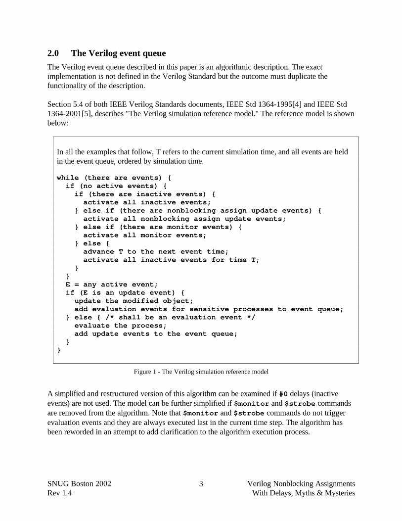
2.0 The Verilog event queue
The Verilog event queue described in this paper is an algorithmic description. The exactimplementation is not defined in the Verilog Standard but the outcome must duplicate thefunctionality of the description.
Section 5.4 of both IEEE Verilog Standards documents, IEEE Std 1364-1995[4] and IEEE Std1364-2001[5], describes "The Verilog simulation reference model." The reference model is shownbelow:
In all the examples that follow, T refers to the current simulation time, and all events are heldin the event queue, ordered by simulation time.
while (there are events) { if (no active events) { if (there are inactive events) { activate all inactive events; } else if (there are nonblocking assign update events) { activate all nonblocking assign update events; } else if (there are monitor events) { activate all monitor events; } else { advance T to the next event time; activate all inactive events for time T; } } E = any active event; if (E is an update event) { update the modified object; add evaluation events for sensitive processes to event queue; } else { /* shall be an evaluation event */ evaluate the process; add update events to the event queue; }}
Figure 1 - The Verilog simulation reference model
A simplified and restructured version of this algorithm can be examined if #0 delays (inactiveevents) are not used. The model can be further simplified if $monitor and $strobe commandsare removed from the algorithm. Note that $monitor and $strobe commands do not triggerevaluation events and they are always executed last in the current time step. The algorithm hasbeen reworded in an attempt to add clarification to the algorithm execution process.
SNUG Boston 2002 Verilog Nonblocking AssignmentsRev 1.4 With Delays, Myths & Mysteries
4
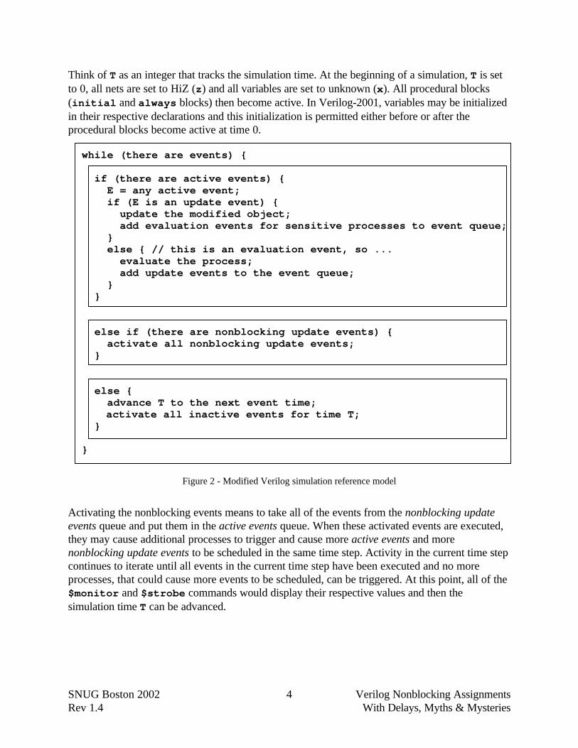
Think of T as an integer that tracks the simulation time. At the beginning of a simulation, T is setto 0, all nets are set to HiZ (z) and all variables are set to unknown (x). All procedural blocks(initial and always blocks) then become active. In Verilog-2001, variables may be initializedin their respective declarations and this initialization is permitted either before or after theprocedural blocks become active at time 0.
while (there are events) {
if (there are active events) { E = any active event; if (E is an update event) { update the modified object; add evaluation events for sensitive processes to event queue; } else { // this is an evaluation event, so ... evaluate the process; add update events to the event queue; } }
else if (there are nonblocking update events) { activate all nonblocking update events; }
else { advance T to the next event time;
activate all inactive events for time T; }
}
Figure 2 - Modified Verilog simulation reference model
Activating the nonblocking events means to take all of the events from the nonblocking updateevents queue and put them in the active events queue. When these activated events are executed,they may cause additional processes to trigger and cause more active events and morenonblocking update events to be scheduled in the same time step. Activity in the current time stepcontinues to iterate until all events in the current time step have been executed and no moreprocesses, that could cause more events to be scheduled, can be triggered. At this point, all of the$monitor and $strobe commands would display their respective values and then thesimulation time T can be advanced.
SNUG Boston 2002 Verilog Nonblocking AssignmentsRev 1.4 With Delays, Myths & Mysteries
5
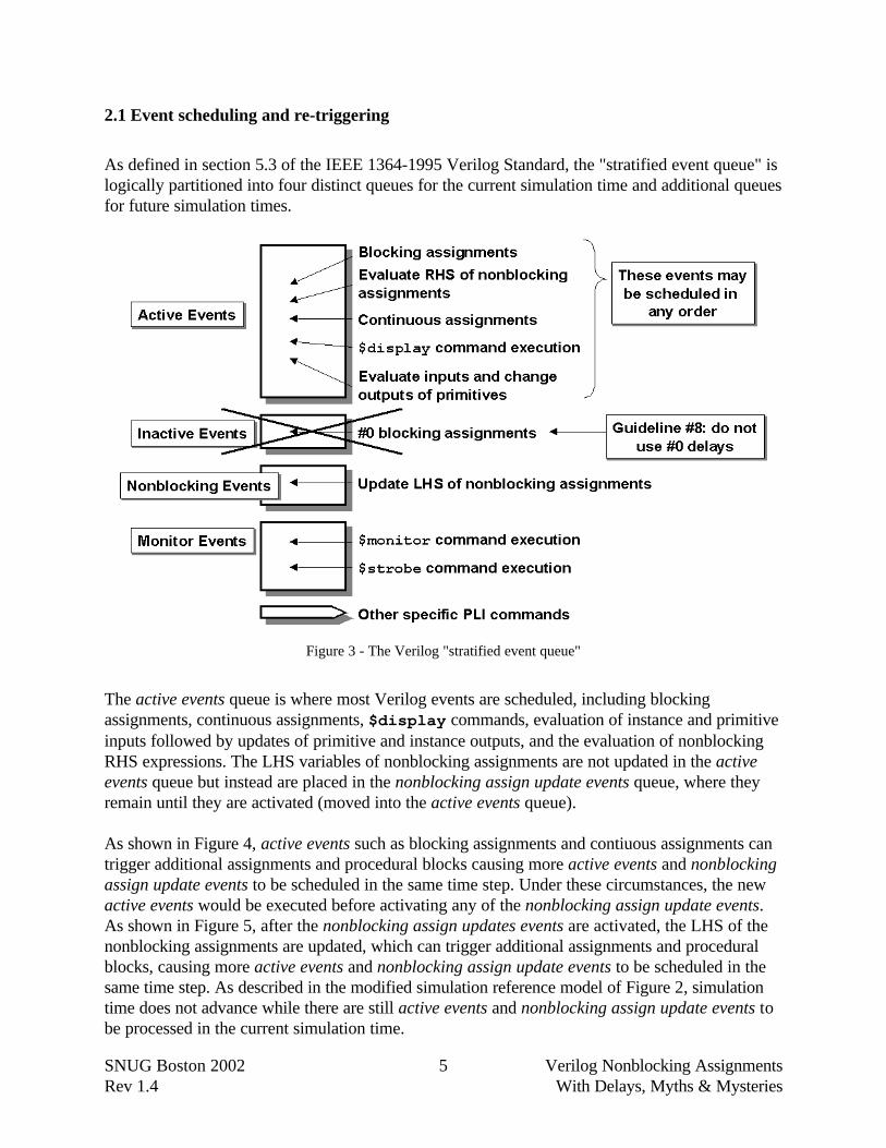
2.1 Event scheduling and re-triggering
As defined in section 5.3 of the IEEE 1364-1995 Verilog Standard, the "stratified event queue" islogically partitioned into four distinct queues for the current simulation time and additional queuesfor future simulation times.
Figure 3 - The Verilog "stratified event queue"
The active events queue is where most Verilog events are scheduled, including blockingassignments, continuous assignments, $display commands, evaluation of instance and primitiveinputs followed by updates of primitive and instance outputs, and the evaluation of nonblockingRHS expressions. The LHS variables of nonblocking assignments are not updated in the activeevents queue but instead are placed in the nonblocking assign update events queue, where theyremain until they are activated (moved into the active events queue).
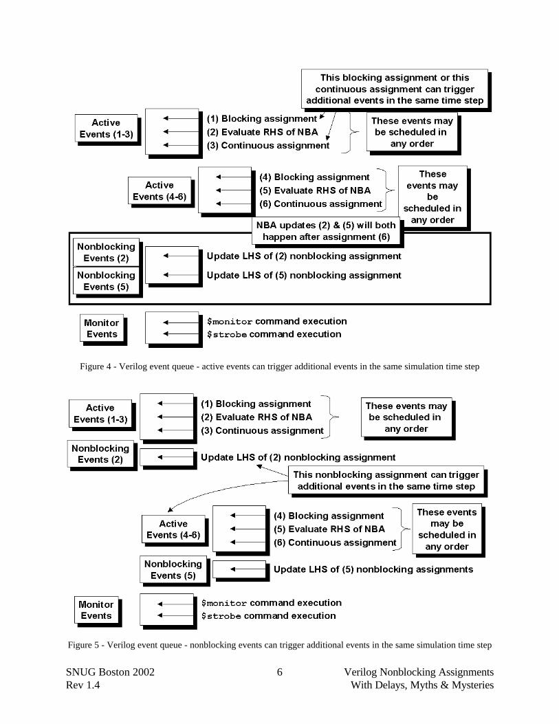
As shown in Figure 4, active events such as blocking assignments and contiuous assignments cantrigger additional assignments and procedural blocks causing more active events and nonblockingassign update events to be scheduled in the same time step. Under these circumstances, the newactive events would be executed before activating any of the nonblocking assign update events.As shown in Figure 5, after the nonblocking assign updates events are activated, the LHS of thenonblocking assignments are updated, which can trigger additional assignments and proceduralblocks, causing more active events and nonblocking assign update events to be scheduled in thesame time step. As described in the modified simulation reference model of Figure 2, simulationtime does not advance while there are still active events and nonblocking assign update events tobe processed in the current simulation time.
SNUG Boston 2002 Verilog Nonblocking AssignmentsRev 1.4 With Delays, Myths & Mysteries
6
Figure 4 - Verilog event queue - active events can trigger additional events in the same simulation time step
Figure 5 - Verilog event queue - nonblocking events can trigger additional events in the same simulation time step
SNUG Boston 2002 Verilog Nonblocking AssignmentsRev 1.4 With Delays, Myths & Mysteries
7
3.0 Review of Important Coding Guidelines with Nonblocking Assignments
In my SNUG2000 San Jose conference paper[2], I mentioned eight important guidelines to followwhen modeling synthesizable logic. For review purposes, the guidelines are included here:
Guideline #1: When modeling sequential logic, use nonblocking assignments.Guideline #2: When modeling latches, use nonblocking assignments.Guideline #3: When modeling combinational logic with an always block, use blocking
assignments.Guideline #4: When modeling both sequential and combinational logic within the same always
block, use nonblocking assignments.Guideline #5: Do not mix blocking and nonblocking assignments in the same always block.Guideline #6: Do not make assignments to the same variable from more than one always block.Guideline #7: Use $strobe to display values that have been assigned using nonblocking
assignments.Guideline #8: Do not make assignments using #0 delays.
Guidelines #1-#4 are now generally recognized to be good and safe coding styles for RTL coding.Guideline #5 has been debated and will be further addressed and justified in section 10.0.Violating guideline #6 will typically yield bizarre mismatches between pre-synthesis and post-synthesis simulations and frequently neither the pre-synthesis nor post-synthesis simulations willbe functionally accurate. Guideline #7 explains how to display the value of an assignment madewith a nonblocking assignment in the same time step as the nonblocking assignment. Guideline #8basically warns that a #0 assignment causes events to be scheduled in an unnecessary intermediateevent queue with often confusing results. In general a #0 assignment is not necessary and shouldnever be used.
Exceptions to these guidelines can be safely implemented, but I would ask myself the followingthree questions when considering exceptions to the recommended coding styles:
1. Does the exception coding style significantly improve simulation performance more than anequivalent coding style that follows the above guidelines? Does it make the simulationsignificantly faster?
2. Does the exception make RTL or verification coding significantly easier to understand than anequivalent coding style that follows the above guidelines? Does it make the code moreunderstandable?
3. Does the exception significantly facilitate RTL or verification coding more than an equivalentcoding style that follows the above guidelines? Does it make the coding effort much easier?
Much faster? More understandable? Easier to code? If not, then the exception is generally notworth making.
SNUG Boston 2002 Verilog Nonblocking AssignmentsRev 1.4 With Delays, Myths & Mysteries
8
Section 10.0 will address these questions with respect to Guideline #5, the guideline from this listthat is most frequently challenged in public forums.
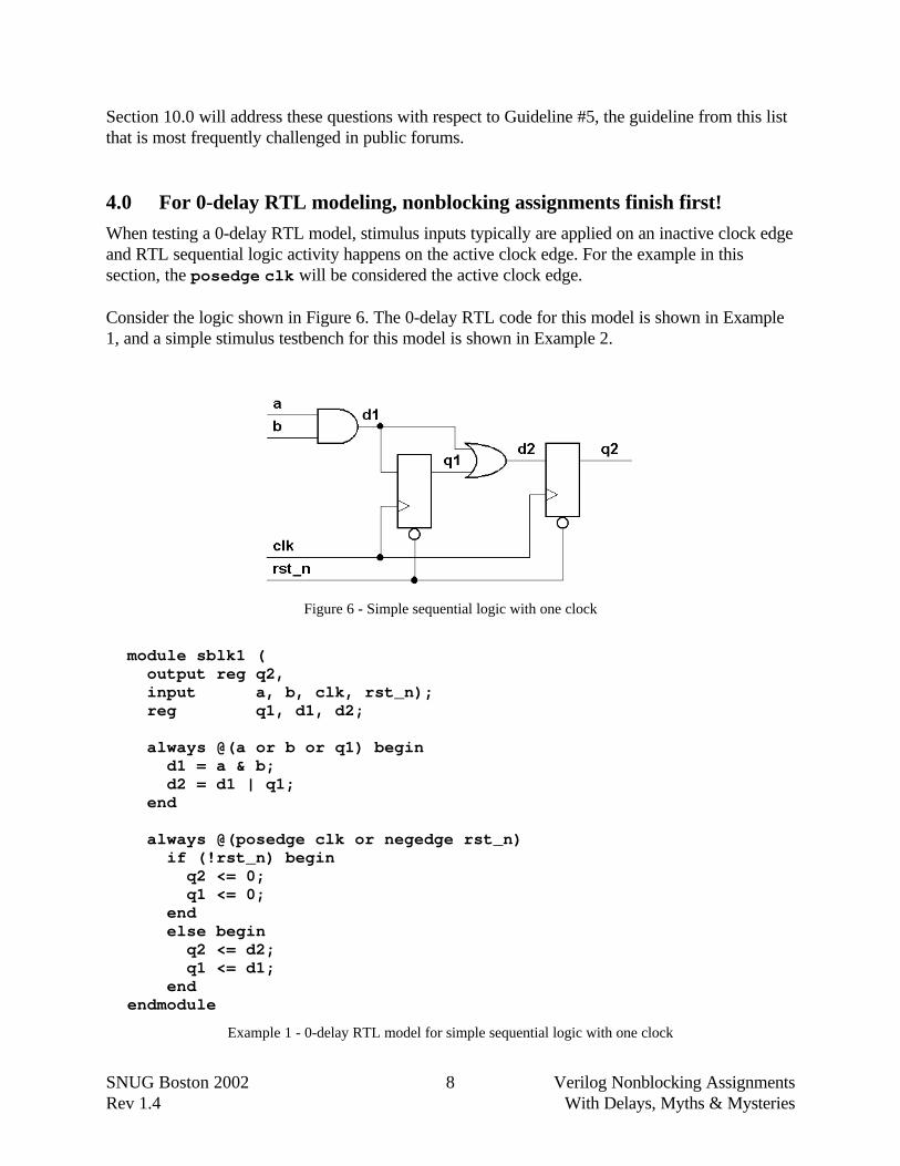
4.0 For 0-delay RTL modeling, nonblocking assignments finish first!
When testing a 0-delay RTL model, stimulus inputs typically are applied on an inactive clock edgeand RTL sequential logic activity happens on the active clock edge. For the example in thissection, the posedge clk will be considered the active clock edge.
Consider the logic shown in Figure 6. The 0-delay RTL code for this model is shown in Example1, and a simple stimulus testbench for this model is shown in Example 2.
Figure 6 - Simple sequential logic with one clock
module sblk1 ( output reg q2, input a, b, clk, rst_n); reg q1, d1, d2;
always @(a or b or q1) begin d1 = a & b; d2 = d1 | q1; end
always @(posedge clk or negedge rst_n) if (!rst_n) begin q2 <= 0; q1 <= 0; end else begin q2 <= d2; q1 <= d1; endendmodule
Example 1 - 0-delay RTL model for simple sequential logic with one clock
SNUG Boston 2002 Verilog Nonblocking AssignmentsRev 1.4 With Delays, Myths & Mysteries
9
module tb; reg a, b, clk, rst_n;
initial begin // clock oscillator clk = 0; forever #10 clk = ~clk; end
sblk1 u1 (.q2(q2), .a(a), .b(b), .clk(clk), .rst_n(rst_n));
initial begin // stimulus a = 0; b = 0; rst_n <= 0; @(posedge clk); @(negedge clk) rst_n = 1; a = 1; b = 1; @(negedge clk) a = 0; @(negedge clk) b = 0; @(negedge clk) $finish; endendmodule
Example 2 - Simple testbench to apply stimulus to the 0-delay RTL model for simple sequential logic
The testbench has a free-running clock oscillator with the clk initialized to 0 for the first half-cycle and the initial block sets initial values for both the a and b inputs and then resets thecircuit until one cycle into the simulation (the first official negedge clk). On the first officialnegedge clk, the reset is removed and the primary inputs to the model, a and b, are bothchanged to 1's. On the next two negedge clks, first the a-input and then the b-input aresuccessively changed to 0's. One negedge clk later the simulation is stopped with a $finishcommand.
From this simple sequence of stimulus inputs, we can see interesting aspects of how stimulus andRTL events are scheduled in the Verilog event queue.
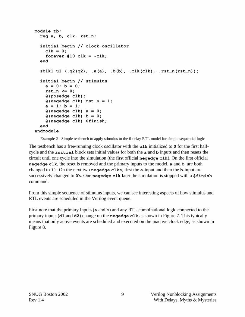
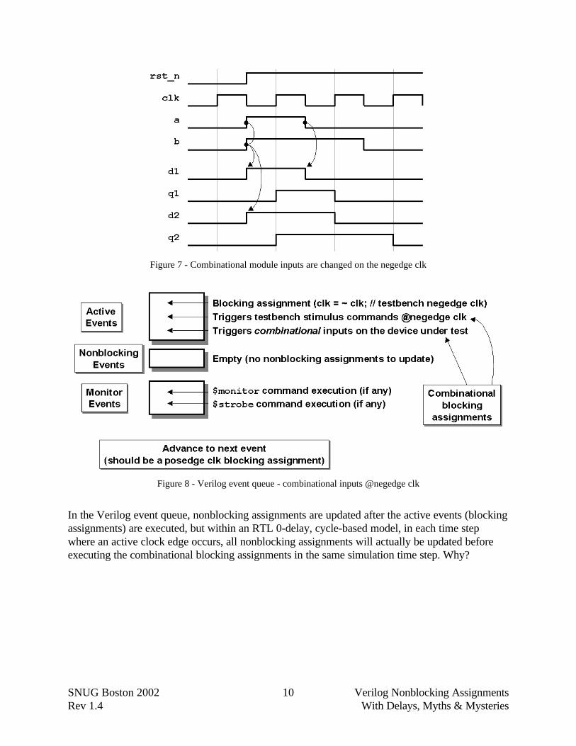
First note that the primary inputs (a and b) and any RTL combinational logic connected to theprimary inputs (d1 and d2) change on the negedge clk as shown in Figure 7. This typicallymeans that only active events are scheduled and executed on the inactive clock edge, as shown inFigure 8.
SNUG Boston 2002 Verilog Nonblocking AssignmentsRev 1.4 With Delays, Myths & Mysteries
10
Figure 7 - Combinational module inputs are changed on the negedge clk
Figure 8 - Verilog event queue - combinational inputs @negedge clk
In the Verilog event queue, nonblocking assignments are updated after the active events (blockingassignments) are executed, but within an RTL 0-delay, cycle-based model, in each time stepwhere an active clock edge occurs, all nonblocking assignments will actually be updated beforeexecuting the combinational blocking assignments in the same simulation time step. Why?
SNUG Boston 2002 Verilog Nonblocking AssignmentsRev 1.4 With Delays, Myths & Mysteries
11
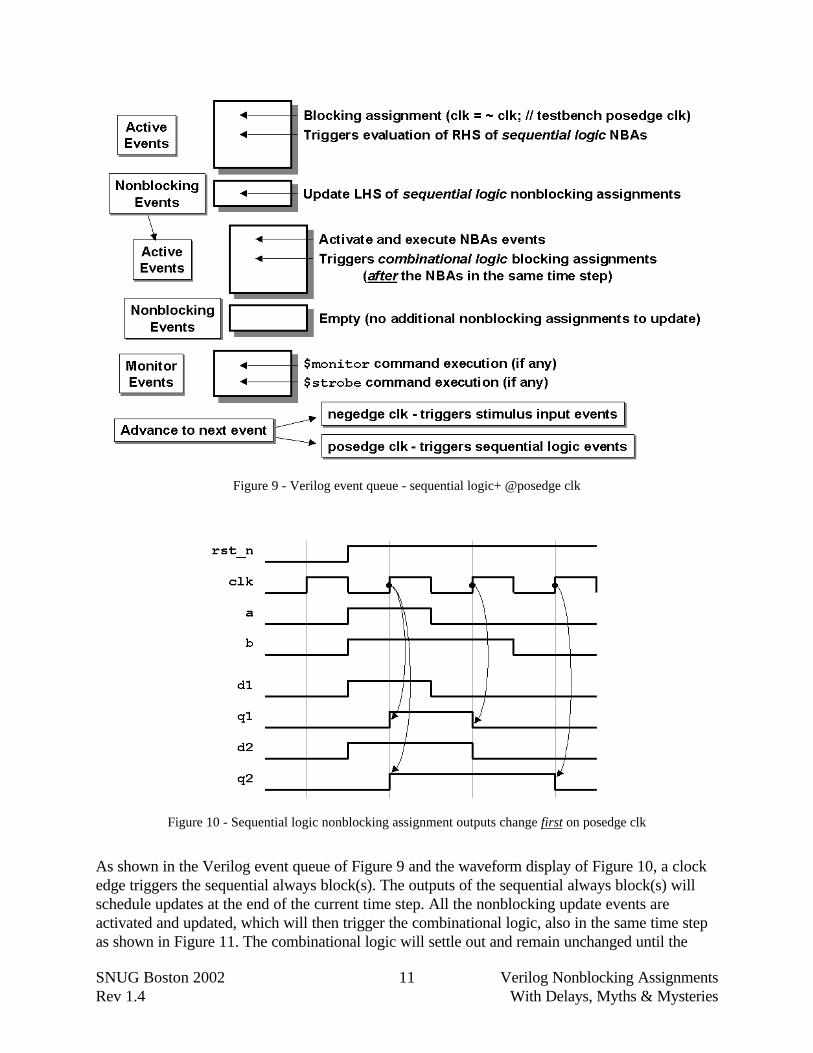
Figure 9 - Verilog event queue - sequential logic+ @posedge clk
Figure 10 - Sequential logic nonblocking assignment outputs change first on posedge clk
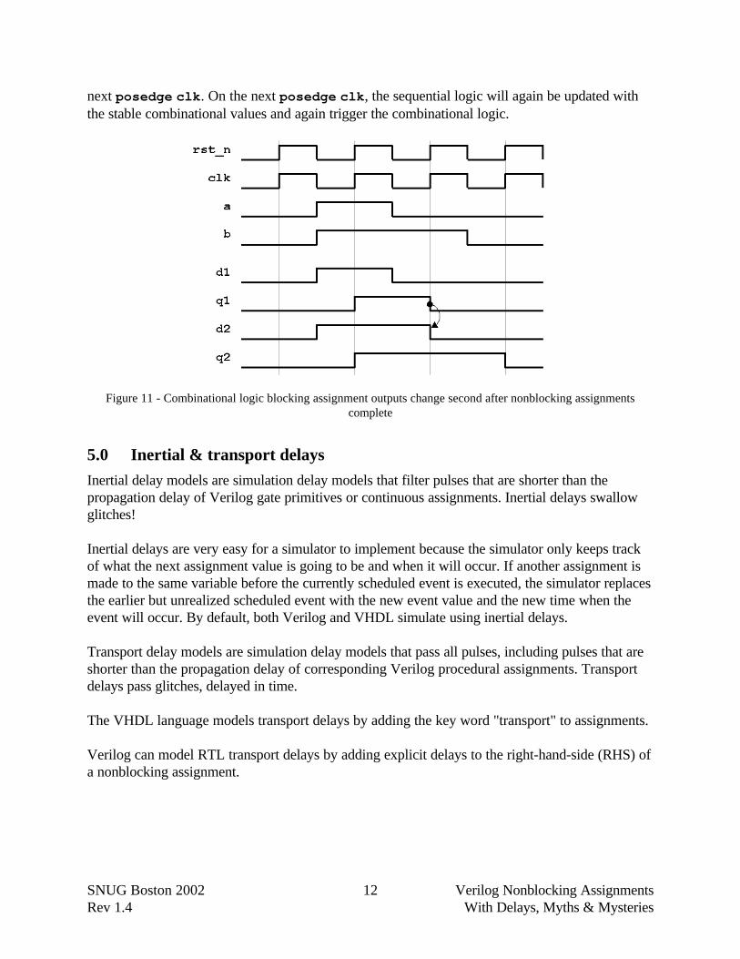
As shown in the Verilog event queue of Figure 9 and the waveform display of Figure 10, a clockedge triggers the sequential always block(s). The outputs of the sequential always block(s) willschedule updates at the end of the current time step. All the nonblocking update events areactivated and updated, which will then trigger the combinational logic, also in the same time stepas shown in Figure 11. The combinational logic will settle out and remain unchanged until the
SNUG Boston 2002 Verilog Nonblocking AssignmentsRev 1.4 With Delays, Myths & Mysteries
12
next posedge clk. On the next posedge clk, the sequential logic will again be updated withthe stable combinational values and again trigger the combinational logic.
Figure 11 - Combinational logic blocking assignment outputs change second after nonblocking assignmentscomplete
5.0 Inertial & transport delays
Inertial delay models are simulation delay models that filter pulses that are shorter than thepropagation delay of Verilog gate primitives or continuous assignments. Inertial delays swallowglitches!
Inertial delays are very easy for a simulator to implement because the simulator only keeps trackof what the next assignment value is going to be and when it will occur. If another assignment ismade to the same variable before the currently scheduled event is executed, the simulator replacesthe earlier but unrealized scheduled event with the new event value and the new time when theevent will occur. By default, both Verilog and VHDL simulate using inertial delays.
Transport delay models are simulation delay models that pass all pulses, including pulses that areshorter than the propagation delay of corresponding Verilog procedural assignments. Transportdelays pass glitches, delayed in time.
The VHDL language models transport delays by adding the key word "transport" to assignments.
Verilog can model RTL transport delays by adding explicit delays to the right-hand-side (RHS) ofa nonblocking assignment.
SNUG Boston 2002 Verilog Nonblocking AssignmentsRev 1.4 With Delays, Myths & Mysteries
13
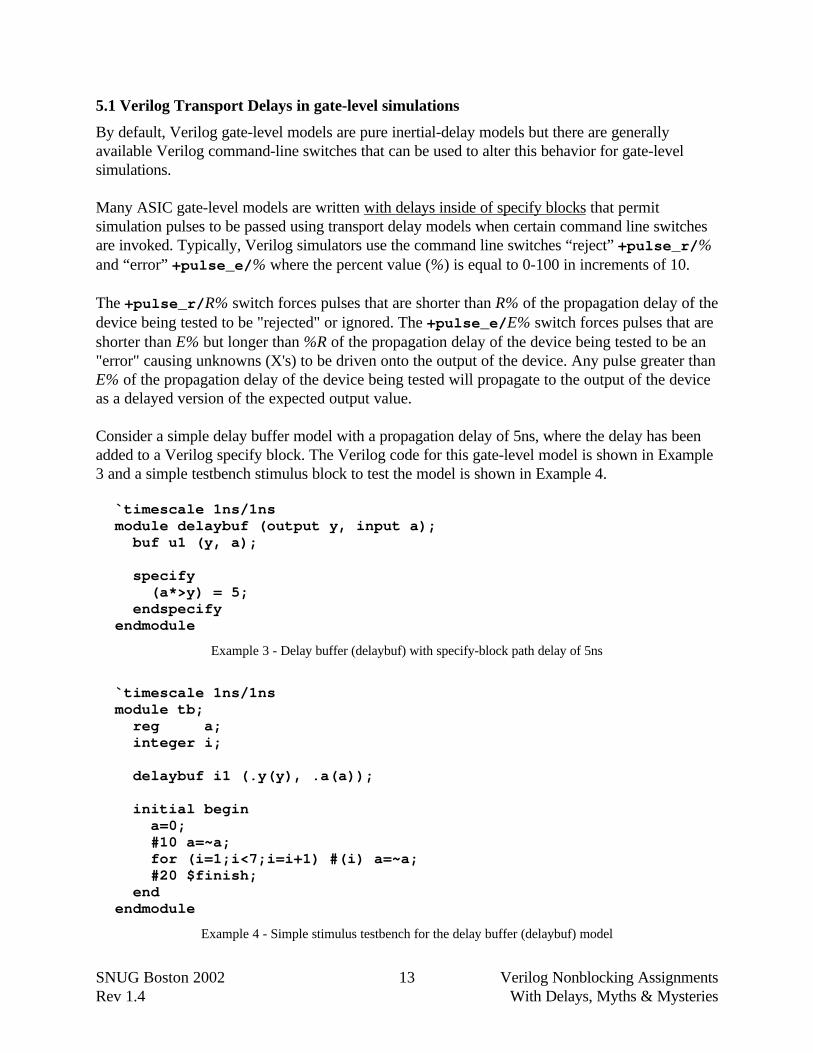
5.1 Verilog Transport Delays in gate-level simulations
By default, Verilog gate-level models are pure inertial-delay models but there are generallyavailable Verilog command-line switches that can be used to alter this behavior for gate-levelsimulations.
Many ASIC gate-level models are written with delays inside of specify blocks that permitsimulation pulses to be passed using transport delay models when certain command line switchesare invoked. Typically, Verilog simulators use the command line switches “reject” +pulse_r/%and “error” +pulse_e/% where the percent value (%) is equal to 0-100 in increments of 10.
The +pulse_r/R% switch forces pulses that are shorter than R% of the propagation delay of thedevice being tested to be "rejected" or ignored. The +pulse_e/E% switch forces pulses that areshorter than E% but longer than %R of the propagation delay of the device being tested to be an"error" causing unknowns (X's) to be driven onto the output of the device. Any pulse greater thanE% of the propagation delay of the device being tested will propagate to the output of the deviceas a delayed version of the expected output value.
Consider a simple delay buffer model with a propagation delay of 5ns, where the delay has beenadded to a Verilog specify block. The Verilog code for this gate-level model is shown in Example3 and a simple testbench stimulus block to test the model is shown in Example 4.
`timescale 1ns/1nsmodule delaybuf (output y, input a); buf u1 (y, a);
specify (a*>y) = 5; endspecifyendmodule
Example 3 - Delay buffer (delaybuf) with specify-block path delay of 5ns
`timescale 1ns/1nsmodule tb; reg a; integer i;
delaybuf i1 (.y(y), .a(a));
initial begin a=0; #10 a=~a; for (i=1;i<7;i=i+1) #(i) a=~a; #20 $finish; endendmodule
Example 4 - Simple stimulus testbench for the delay buffer (delaybuf) model
SNUG Boston 2002 Verilog Nonblocking AssignmentsRev 1.4 With Delays, Myths & Mysteries
14
For this delaybuf model, the default will be a pure inertial delay-mode simulation and all inputpulses less than 5ns in width will be filtered or ignored.
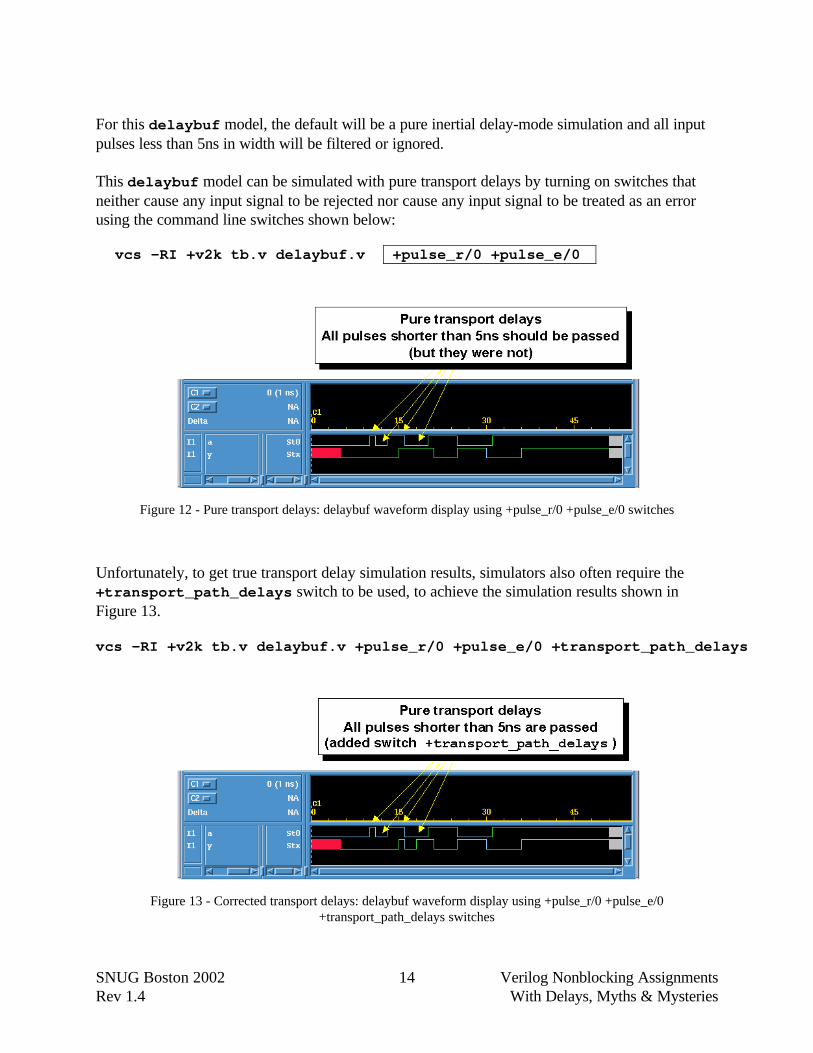
This delaybuf model can be simulated with pure transport delays by turning on switches thatneither cause any input signal to be rejected nor cause any input signal to be treated as an errorusing the command line switches shown below:
vcs -RI +v2k tb.v delaybuf.v +pulse_r/0 +pulse_e/0
Figure 12 - Pure transport delays: delaybuf waveform display using +pulse_r/0 +pulse_e/0 switches
Unfortunately, to get true transport delay simulation results, simulators also often require the+transport_path_delays switch to be used, to achieve the simulation results shown inFigure 13.
vcs -RI +v2k tb.v delaybuf.v +pulse_r/0 +pulse_e/0 +transport_path_delays
Figure 13 - Corrected transport delays: delaybuf waveform display using +pulse_r/0 +pulse_e/0+transport_path_delays switches
SNUG Boston 2002 Verilog Nonblocking AssignmentsRev 1.4 With Delays, Myths & Mysteries
15
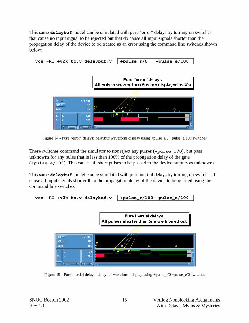
This same delaybuf model can be simulated with pure "error" delays by turning on switchesthat cause no input signal to be rejected but that do cause all input signals shorter than thepropagation delay of the device to be treated as an error using the command line switches shownbelow:
vcs -RI +v2k tb.v delaybuf.v +pulse_r/0 +pulse_e/100
Figure 14 - Pure "error" delays: delaybuf waveform display using +pulse_r/0 +pulse_e/100 switches
These switches command the simulator to not reject any pulses (+pulse_r/0), but passunknowns for any pulse that is less than 100% of the propagation delay of the gate(+pulse_e/100). This causes all short pulses to be passed to the device outputs as unknowns.
This same delaybuf model can be simulated with pure inertial delays by turning on switches thatcause all input signals shorter than the propagation delay of the device to be ignored using thecommand line switches:
vcs -RI +v2k tb.v delaybuf.v +pulse_r/100 +pulse_e/100
Figure 15 - Pure inertial delays: delaybuf waveform display using +pulse_r/0 +pulse_e/0 switches
SNUG Boston 2002 Verilog Nonblocking AssignmentsRev 1.4 With Delays, Myths & Mysteries
16
The first switch commands the simulator to reject any input pulse shorter than 100% of thepropagation delay of the device (+pulse_r/100). Since the percentage of the "error" switchmatches the percentage of the "reject" switch, this forces the simulator to not pass unknowns tothe outputs of the device. This is a pure inertial delay model style.
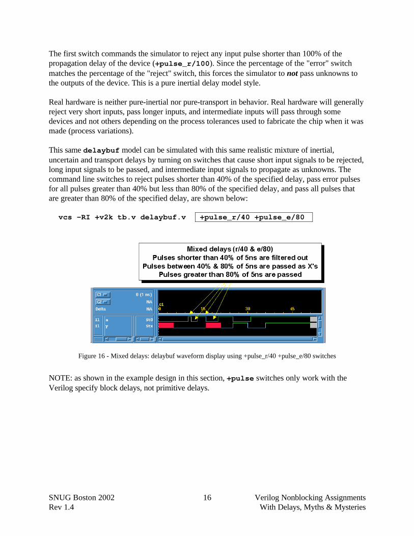
Real hardware is neither pure-inertial nor pure-transport in behavior. Real hardware will generallyreject very short inputs, pass longer inputs, and intermediate inputs will pass through somedevices and not others depending on the process tolerances used to fabricate the chip when it wasmade (process variations).
This same delaybuf model can be simulated with this same realistic mixture of inertial,uncertain and transport delays by turning on switches that cause short input signals to be rejected,long input signals to be passed, and intermediate input signals to propagate as unknowns. Thecommand line switches to reject pulses shorter than 40% of the specified delay, pass error pulsesfor all pulses greater than 40% but less than 80% of the specified delay, and pass all pulses thatare greater than 80% of the specified delay, are shown below:
vcs -RI +v2k tb.v delaybuf.v +pulse_r/40 +pulse_e/80
Figure 16 - Mixed delays: delaybuf waveform display using +pulse_r/40 +pulse_e/80 switches
NOTE: as shown in the example design in this section, +pulse switches only work with theVerilog specify block delays, not primitive delays.
SNUG Boston 2002 Verilog Nonblocking AssignmentsRev 1.4 With Delays, Myths & Mysteries
17
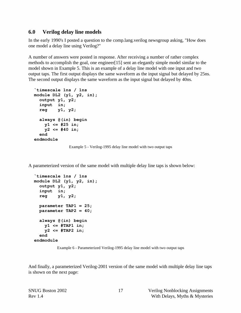
6.0 Verilog delay line models
In the early 1990's I posted a question to the comp.lang.verilog newsgroup asking, "How doesone model a delay line using Verilog?"
A number of answers were posted in response. After receiving a number of rather complexmethods to accomplish the goal, one engineer[15] sent an elegantly simple model similar to themodel shown in Example 5. This is an example of a delay line model with one input and twooutput taps. The first output displays the same waveform as the input signal but delayed by 25ns.The second output displays the same waveform as the input signal but delayed by 40ns.
`timescale 1ns / 1nsmodule DL2 (y1, y2, in); output y1, y2; input in; reg y1, y2;
always @(in) begin y1 <= #25 in; y2 <= #40 in; endendmodule
Example 5 - Verilog-1995 delay line model with two output taps
A parameterized version of the same model with multiple delay line taps is shown below:
`timescale 1ns / 1nsmodule DL2 (y1, y2, in); output y1, y2; input in; reg y1, y2;
parameter TAP1 = 25; parameter TAP2 = 40;
always @(in) begin y1 <= #TAP1 in; y2 <= #TAP2 in; endendmodule
Example 6 - Parameterized Verilog-1995 delay line model with two output taps
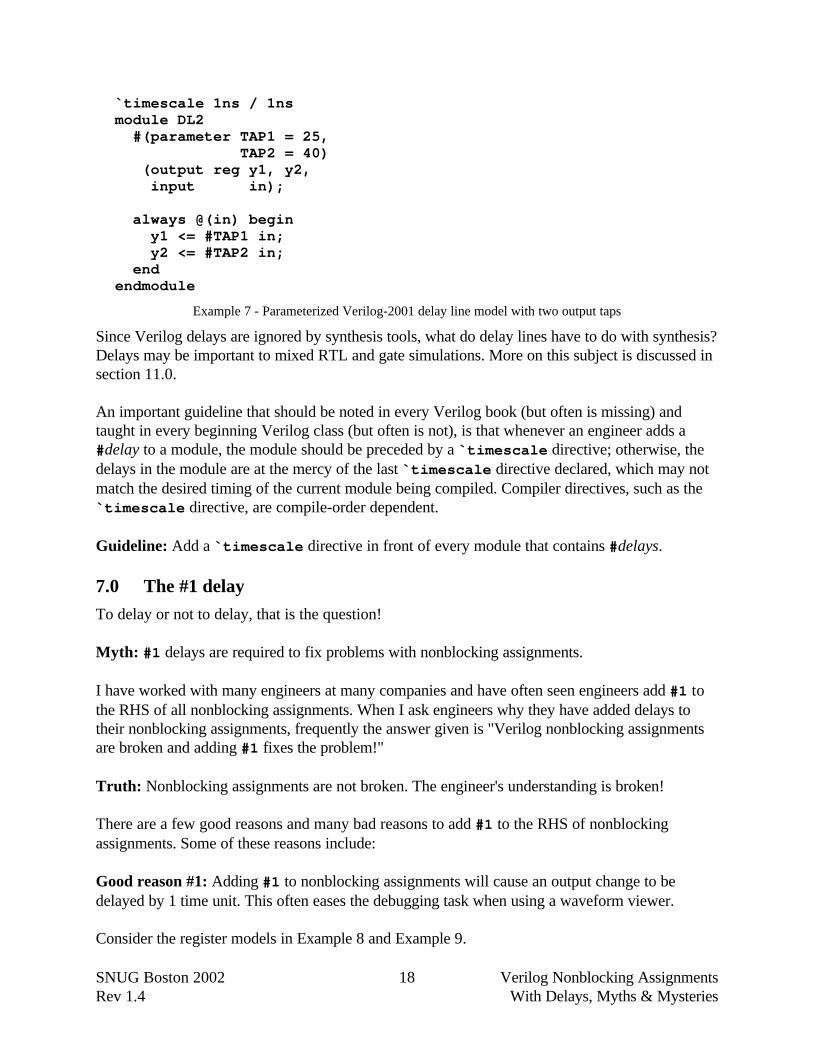
And finally, a parameterized Verilog-2001 version of the same model with multiple delay line tapsis shown on the next page:
SNUG Boston 2002 Verilog Nonblocking AssignmentsRev 1.4 With Delays, Myths & Mysteries
18
`timescale 1ns / 1nsmodule DL2 #(parameter TAP1 = 25, TAP2 = 40) (output reg y1, y2, input in);
always @(in) begin y1 <= #TAP1 in; y2 <= #TAP2 in; endendmodule
Example 7 - Parameterized Verilog-2001 delay line model with two output taps
Since Verilog delays are ignored by synthesis tools, what do delay lines have to do with synthesis?Delays may be important to mixed RTL and gate simulations. More on this subject is discussed insection 11.0.
An important guideline that should be noted in every Verilog book (but often is missing) andtaught in every beginning Verilog class (but often is not), is that whenever an engineer adds a#delay to a module, the module should be preceded by a `timescale directive; otherwise, thedelays in the module are at the mercy of the last `timescale directive declared, which may notmatch the desired timing of the current module being compiled. Compiler directives, such as the`timescale directive, are compile-order dependent.
Guideline: Add a `timescale directive in front of every module that contains #delays.
7.0 The #1 delay
To delay or not to delay, that is the question!
Myth: #1 delays are required to fix problems with nonblocking assignments.
I have worked with many engineers at many companies and have often seen engineers add #1 tothe RHS of all nonblocking assignments. When I ask engineers why they have added delays totheir nonblocking assignments, frequently the answer given is "Verilog nonblocking assignmentsare broken and adding #1 fixes the problem!"
Truth: Nonblocking assignments are not broken. The engineer's understanding is broken!
There are a few good reasons and many bad reasons to add #1 to the RHS of nonblockingassignments. Some of these reasons include:
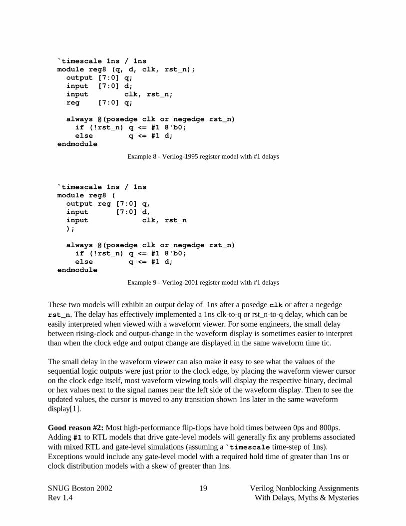
Good reason #1: Adding #1 to nonblocking assignments will cause an output change to bedelayed by 1 time unit. This often eases the debugging task when using a waveform viewer.
Consider the register models in Example 8 and Example 9.
SNUG Boston 2002 Verilog Nonblocking AssignmentsRev 1.4 With Delays, Myths & Mysteries
19
`timescale 1ns / 1nsmodule reg8 (q, d, clk, rst_n); output [7:0] q; input [7:0] d; input clk, rst_n; reg [7:0] q;
always @(posedge clk or negedge rst_n) if (!rst_n) q <= #1 8'b0; else q <= #1 d;endmodule
Example 8 - Verilog-1995 register model with #1 delays
`timescale 1ns / 1nsmodule reg8 ( output reg [7:0] q, input [7:0] d, input clk, rst_n );
always @(posedge clk or negedge rst_n) if (!rst_n) q <= #1 8'b0; else q <= #1 d;endmodule
Example 9 - Verilog-2001 register model with #1 delays
These two models will exhibit an output delay of 1ns after a posedge clk or after a negedgerst_n. The delay has effectively implemented a 1ns clk-to-q or rst_n-to-q delay, which can beeasily interpreted when viewed with a waveform viewer. For some engineers, the small delaybetween rising-clock and output-change in the waveform display is sometimes easier to interpretthan when the clock edge and output change are displayed in the same waveform time tic.
The small delay in the waveform viewer can also make it easy to see what the values of thesequential logic outputs were just prior to the clock edge, by placing the waveform viewer cursoron the clock edge itself, most waveform viewing tools will display the respective binary, decimalor hex values next to the signal names near the left side of the waveform display. Then to see theupdated values, the cursor is moved to any transition shown 1ns later in the same waveformdisplay[1].
Good reason #2: Most high-performance flip-flops have hold times between 0ps and 800ps.Adding #1 to RTL models that drive gate-level models will generally fix any problems associatedwith mixed RTL and gate-level simulations (assuming a `timescale time-step of 1ns).Exceptions would include any gate-level model with a required hold time of greater than 1ns orclock distribution models with a skew of greater than 1ns.
SNUG Boston 2002 Verilog Nonblocking AssignmentsRev 1.4 With Delays, Myths & Mysteries
20
Bad reason #1: "Verilog nonblocking assignments are broken!" WRONG! Nonblockingassignments work fine, even without RHS #1 delays. If you add delays to the RHS ofnonblocking assignments without knowing the correct reason for adding the delays, at some pointyou will likely run into problems with mixed RTL and gate-level simulations where the gate-levelmodel has hold time delays in excess of 1ns, or the clock distribution network has a skew ofgreater than 1ns, and the simulation will fail.
Bad reason #2: VCS has built-in optimizations for high-speed cycle-based simulation and somecycle-based simulators, like VCS, slow down significantly when #1 delays are added to the RHSof nonblocking assignments.
8.0 VCS simulation benchmarks using #1 delays
If you could dramatically improve the performance of your simulator by making one small RTL-coding change to your designs, would you be interested?
What is the impact to VCS simulation performance by adding #1 delays to the RHS nonblockingassignments?
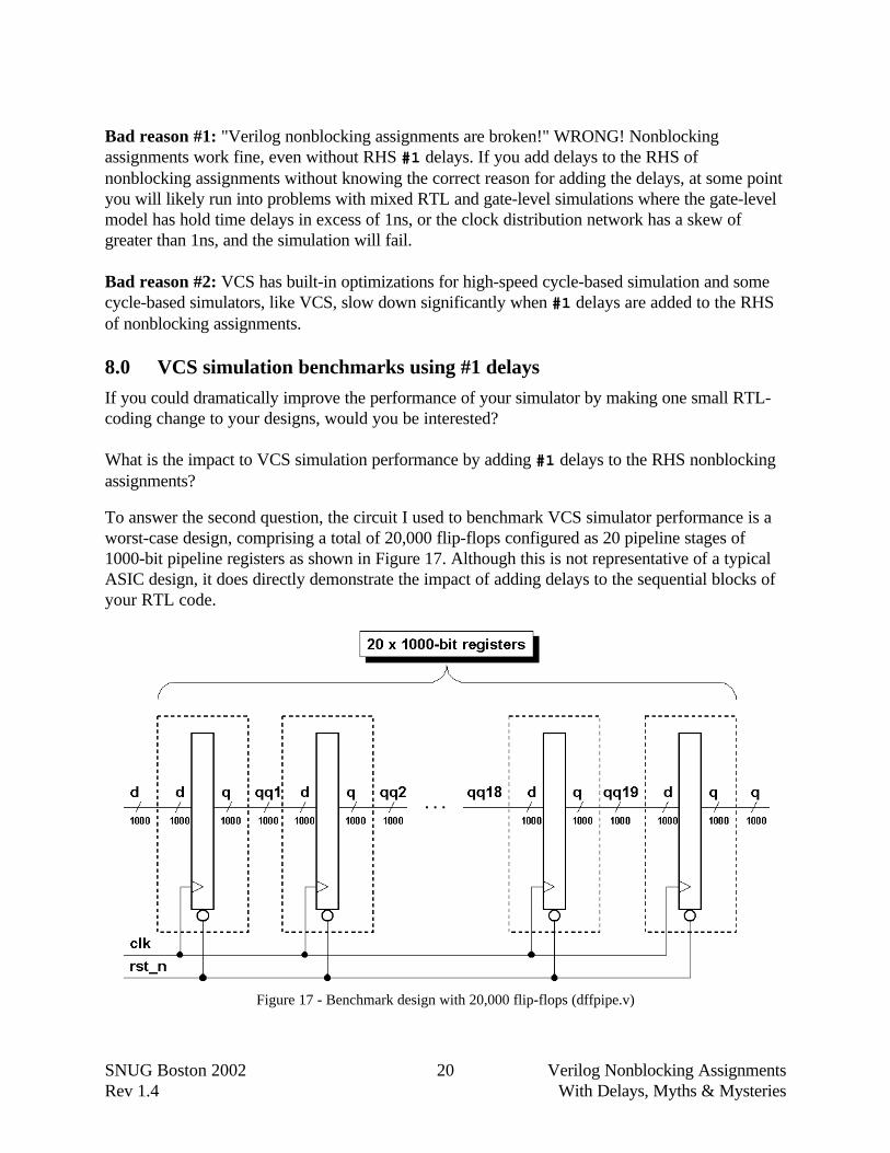
To answer the second question, the circuit I used to benchmark VCS simulator performance is aworst-case design, comprising a total of 20,000 flip-flops configured as 20 pipeline stages of1000-bit pipeline registers as shown in Figure 17. Although this is not representative of a typicalASIC design, it does directly demonstrate the impact of adding delays to the sequential blocks ofyour RTL code.
Figure 17 - Benchmark design with 20,000 flip-flops (dffpipe.v)
SNUG Boston 2002 Verilog Nonblocking AssignmentsRev 1.4 With Delays, Myths & Mysteries
21
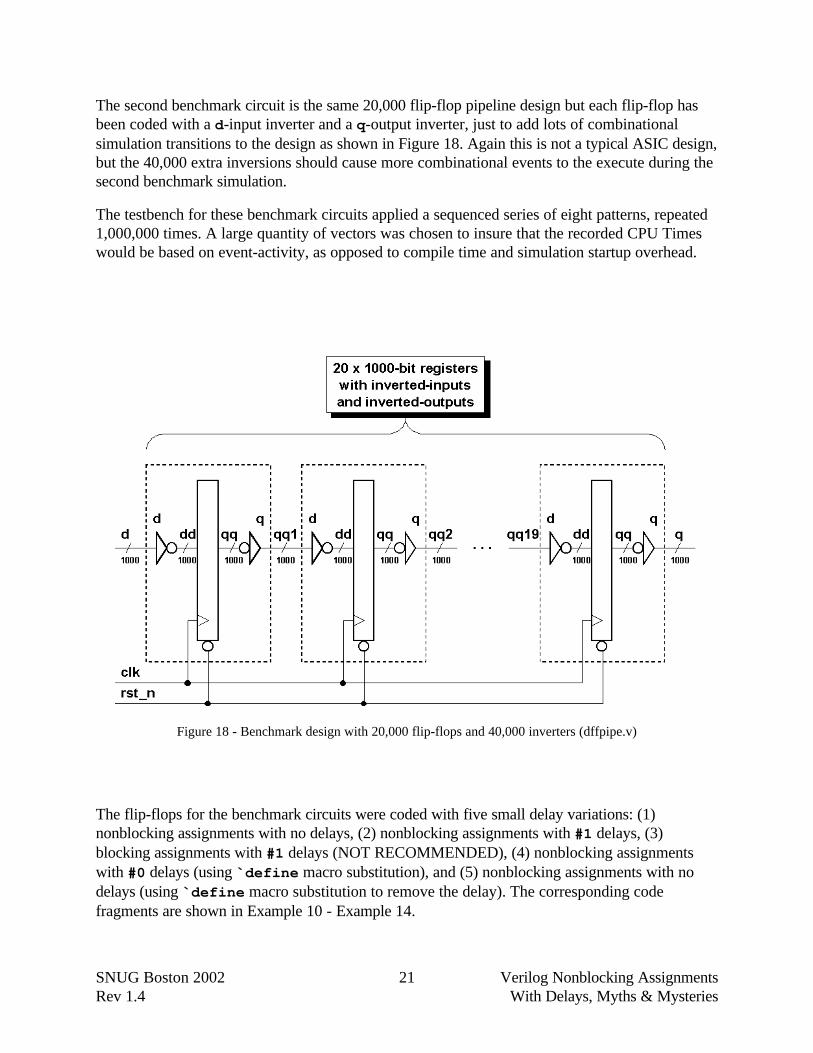
The second benchmark circuit is the same 20,000 flip-flop pipeline design but each flip-flop hasbeen coded with a d-input inverter and a q-output inverter, just to add lots of combinationalsimulation transitions to the design as shown in Figure 18. Again this is not a typical ASIC design,but the 40,000 extra inversions should cause more combinational events to the execute during thesecond benchmark simulation.
The testbench for these benchmark circuits applied a sequenced series of eight patterns, repeated1,000,000 times. A large quantity of vectors was chosen to insure that the recorded CPU Timeswould be based on event-activity, as opposed to compile time and simulation startup overhead.
Figure 18 - Benchmark design with 20,000 flip-flops and 40,000 inverters (dffpipe.v)
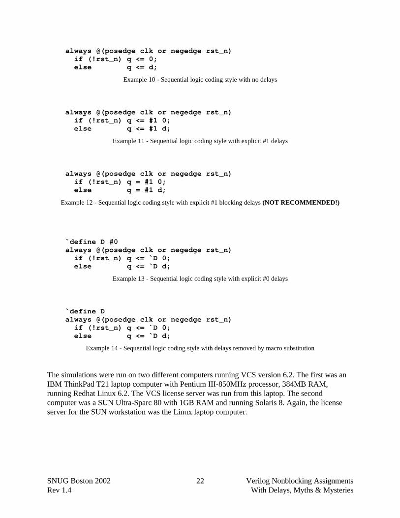
The flip-flops for the benchmark circuits were coded with five small delay variations: (1)nonblocking assignments with no delays, (2) nonblocking assignments with #1 delays, (3)blocking assignments with #1 delays (NOT RECOMMENDED), (4) nonblocking assignmentswith #0 delays (using `define macro substitution), and (5) nonblocking assignments with nodelays (using `define macro substitution to remove the delay). The corresponding codefragments are shown in Example 10 - Example 14.
SNUG Boston 2002 Verilog Nonblocking AssignmentsRev 1.4 With Delays, Myths & Mysteries
22
always @(posedge clk or negedge rst_n) if (!rst_n) q <= 0; else q <= d;
Example 10 - Sequential logic coding style with no delays
always @(posedge clk or negedge rst_n) if (!rst_n) q <= #1 0; else q <= #1 d;
Example 11 - Sequential logic coding style with explicit #1 delays
always @(posedge clk or negedge rst_n) if (!rst_n) q = #1 0; else q = #1 d;
Example 12 - Sequential logic coding style with explicit #1 blocking delays (NOT RECOMMENDED!)
`define D #0 always @(posedge clk or negedge rst_n) if (!rst_n) q <= `D 0; else q <= `D d;
Example 13 - Sequential logic coding style with explicit #0 delays
`define D always @(posedge clk or negedge rst_n) if (!rst_n) q <= `D 0; else q <= `D d;
Example 14 - Sequential logic coding style with delays removed by macro substitution
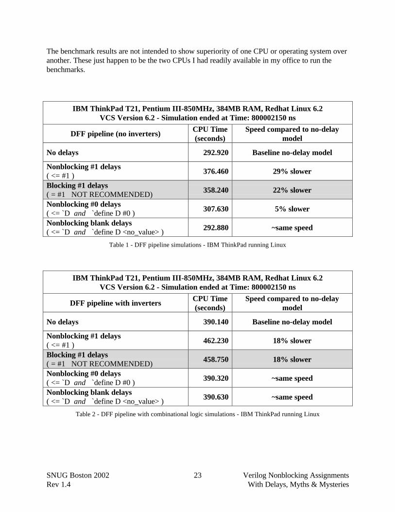
The simulations were run on two different computers running VCS version 6.2. The first was anIBM ThinkPad T21 laptop computer with Pentium III-850MHz processor, 384MB RAM,running Redhat Linux 6.2. The VCS license server was run from this laptop. The secondcomputer was a SUN Ultra-Sparc 80 with 1GB RAM and running Solaris 8. Again, the licenseserver for the SUN workstation was the Linux laptop computer.
SNUG Boston 2002 Verilog Nonblocking AssignmentsRev 1.4 With Delays, Myths & Mysteries
23
The benchmark results are not intended to show superiority of one CPU or operating system overanother. These just happen to be the two CPUs I had readily available in my office to run thebenchmarks.
IBM ThinkPad T21, Pentium III-850MHz, 384MB RAM, Redhat Linux 6.2VCS Version 6.2 - Simulation ended at Time: 800002150 ns
DFF pipeline (no inverters)CPU Time(seconds)
Speed compared to no-delaymodel
No delays 292.920 Baseline no-delay model
Nonblocking #1 delays( <= #1 )
376.460 29% slower
Blocking #1 delays( = #1 NOT RECOMMENDED)
358.240 22% slower
Nonblocking #0 delays( <= `D and `define D #0 )
307.630 5% slower
Nonblocking blank delays( <= `D and `define D <no_value> )
292.880 ~same speed
Table 1 - DFF pipeline simulations - IBM ThinkPad running Linux
IBM ThinkPad T21, Pentium III-850MHz, 384MB RAM, Redhat Linux 6.2VCS Version 6.2 - Simulation ended at Time: 800002150 ns
DFF pipeline with invertersCPU Time(seconds)
Speed compared to no-delaymodel
No delays 390.140 Baseline no-delay model
Nonblocking #1 delays( <= #1 )
462.230 18% slower
Blocking #1 delays( = #1 NOT RECOMMENDED)
458.750 18% slower
Nonblocking #0 delays( <= `D and `define D #0 )
390.320 ~same speed
Nonblocking blank delays( <= `D and `define D <no_value> )
390.630 ~same speed
Table 2 - DFF pipeline with combinational logic simulations - IBM ThinkPad running Linux
SNUG Boston 2002 Verilog Nonblocking AssignmentsRev 1.4 With Delays, Myths & Mysteries
24
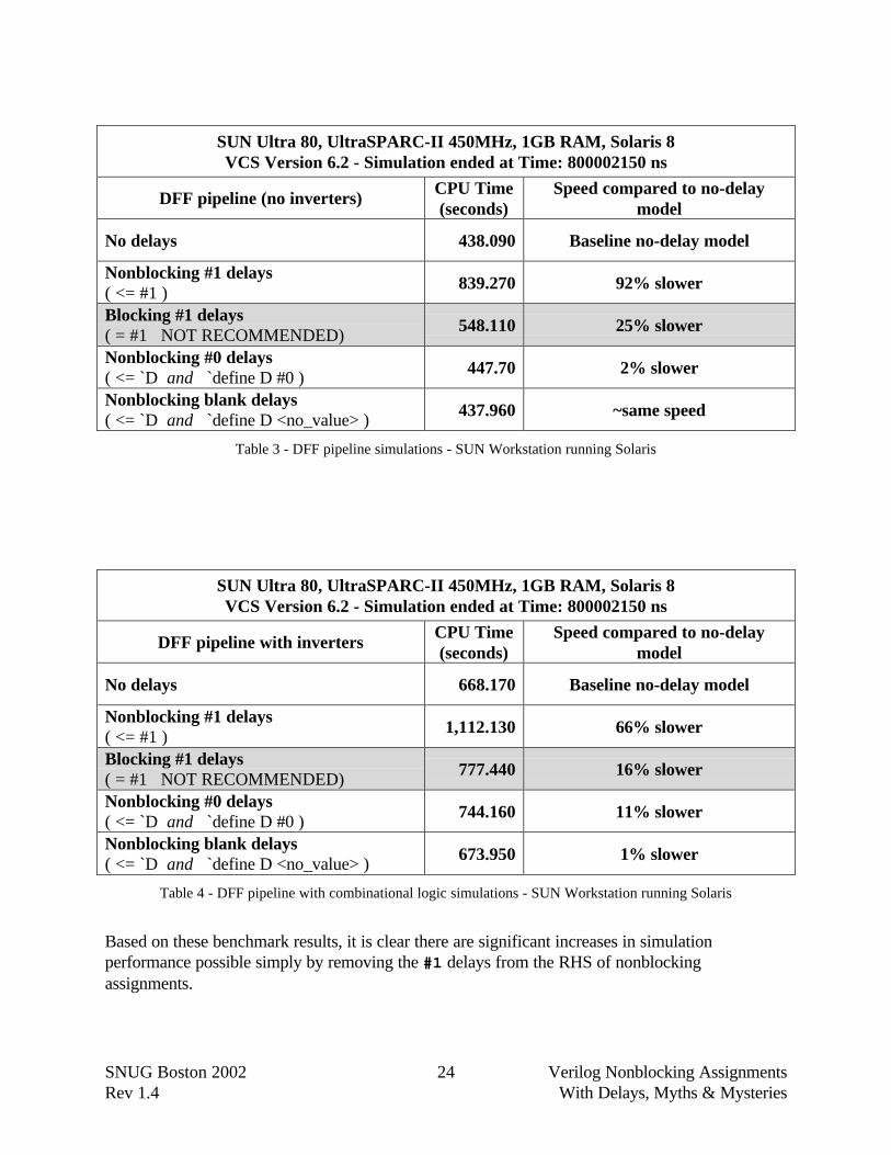
SUN Ultra 80, UltraSPARC-II 450MHz, 1GB RAM, Solaris 8VCS Version 6.2 - Simulation ended at Time: 800002150 ns
DFF pipeline (no inverters)CPU Time(seconds)
Speed compared to no-delaymodel
No delays 438.090 Baseline no-delay model
Nonblocking #1 delays( <= #1 )
839.270 92% slower
Blocking #1 delays( = #1 NOT RECOMMENDED)
548.110 25% slower
Nonblocking #0 delays( <= `D and `define D #0 )
447.70 2% slower
Nonblocking blank delays( <= `D and `define D <no_value> )
437.960 ~same speed
Table 3 - DFF pipeline simulations - SUN Workstation running Solaris
SUN Ultra 80, UltraSPARC-II 450MHz, 1GB RAM, Solaris 8VCS Version 6.2 - Simulation ended at Time: 800002150 ns
DFF pipeline with invertersCPU Time(seconds)
Speed compared to no-delaymodel
No delays 668.170 Baseline no-delay model
Nonblocking #1 delays( <= #1 )
1,112.130 66% slower
Blocking #1 delays( = #1 NOT RECOMMENDED)
777.440 16% slower
Nonblocking #0 delays( <= `D and `define D #0 )
744.160 11% slower
Nonblocking blank delays( <= `D and `define D <no_value> )
673.950 1% slower
Table 4 - DFF pipeline with combinational logic simulations - SUN Workstation running Solaris
Based on these benchmark results, it is clear there are significant increases in simulationperformance possible simply by removing the #1 delays from the RHS of nonblockingassignments.
SNUG Boston 2002 Verilog Nonblocking AssignmentsRev 1.4 With Delays, Myths & Mysteries
25
8.1 Conditionally compiled #1 delays
For engineers interested in retaining the #1 delays for debugging purposes, I recommend that the#1 delays be added to all designs using a common macro definition as shown in Example 15, andcode all sequential logic using `D values on the RHS of nonblocking assignments as shown inExample 16. `D was chosen because "D" stands for delay and it is also very short (half as manycharacters as typing `DLY).
// To enable <= #1 (NonBlocking Delays), simulate with the// following command: +define+NBD// Default is to simulate with the higher performance no-delay`ifdef NBD `define D #1`else `define D`endif
Example 15 - Macro definitions for no-delay and explicit #1-delay simulations
// Typical sequential logic coding stylealways @(posedge clk or negedge rst_n) if (!rst_n) q <= `D 0; else q <= `D d;
Example 16 - Typical sequential logic coding style
Using the code from Example 15 and Example 16 with the command line switch +define+NBD(NBD: NonBlocking Delays) would make all properly coded sequential logic behave equivalent tothe code shown in Example 17, with added #1 delays and degraded simulation performance.
// With +define+NBD - the equivalent code is:// *** slower simulations ***always @(posedge clk or negedge rst_n) if (!rst_n) q <= #1 0; else q <= #1 d;
Example 17 - Equivalent sequential logic coding style after #1 macro substitution
Using the code from Example 15 and Example 16 without the command line switch+define+NBD would make all properly coded sequential logic behave equivalent to the codeshown in Example 18, with no delays and significantly increased simulation performance.
// With NO +define+NBD - the equivalent code is:// *** faster simulations ***always @(posedge clk or negedge rst_n) if (!rst_n) q <= 0; else q <= d;
Example 18 - Equivalent sequential logic coding style after no-delay macro substitution
SNUG Boston 2002 Verilog Nonblocking AssignmentsRev 1.4 With Delays, Myths & Mysteries
26
NOTE: After sharing this benchmark information with Mark Warren, Technical Director of theVerification Group at Synopsys, Mark wanted me to note that VCS simulations of a typicaldesign could experience a 0%-200% increase in simulation performance with a 30%-50% increasebeing typical, as opposed to the 18%-92% increase reported with the contrived benchmarkcircuits in this section[12].
The ratio of combinational logic to sequential logic in an actual ASIC design and the possibleinclusion of PLI code could indeed mean that the percentage improvement in simulationperformance would in all likelihood be closer to the 30%-50% figure. However, it is interesting toobserve the tremendous difference in simulator performance related to adding #1 delays to thenonblocking assignments.
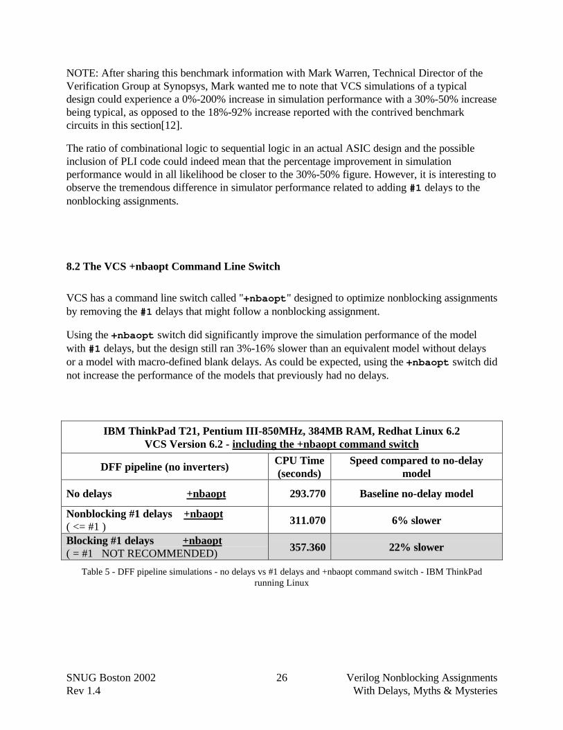
8.2 The VCS +nbaopt Command Line Switch
VCS has a command line switch called "+nbaopt" designed to optimize nonblocking assignmentsby removing the #1 delays that might follow a nonblocking assignment.
Using the +nbaopt switch did significantly improve the simulation performance of the modelwith #1 delays, but the design still ran 3%-16% slower than an equivalent model without delaysor a model with macro-defined blank delays. As could be expected, using the +nbaopt switch didnot increase the performance of the models that previously had no delays.
IBM ThinkPad T21, Pentium III-850MHz, 384MB RAM, Redhat Linux 6.2VCS Version 6.2 - including the +nbaopt command switch
DFF pipeline (no inverters)CPU Time(seconds)
Speed compared to no-delaymodel
No delays +nbaopt 293.770 Baseline no-delay model
Nonblocking #1 delays +nbaopt( <= #1 )
311.070 6% slower
Blocking #1 delays +nbaopt( = #1 NOT RECOMMENDED)
357.360 22% slower
Table 5 - DFF pipeline simulations - no delays vs #1 delays and +nbaopt command switch - IBM ThinkPadrunning Linux
SNUG Boston 2002 Verilog Nonblocking AssignmentsRev 1.4 With Delays, Myths & Mysteries
27
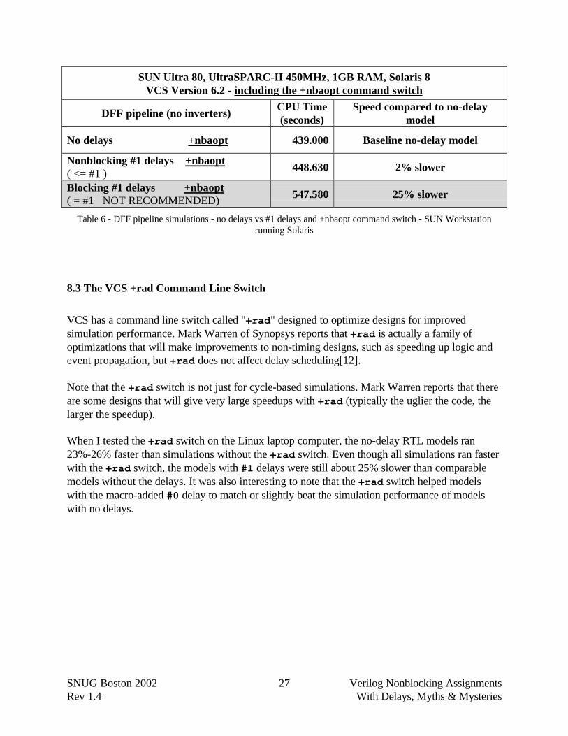
SUN Ultra 80, UltraSPARC-II 450MHz, 1GB RAM, Solaris 8VCS Version 6.2 - including the +nbaopt command switch
DFF pipeline (no inverters)CPU Time(seconds)
Speed compared to no-delaymodel
No delays +nbaopt 439.000 Baseline no-delay model
Nonblocking #1 delays +nbaopt( <= #1 )
448.630 2% slower
Blocking #1 delays +nbaopt( = #1 NOT RECOMMENDED)
547.580 25% slower
Table 6 - DFF pipeline simulations - no delays vs #1 delays and +nbaopt command switch - SUN Workstationrunning Solaris
8.3 The VCS +rad Command Line Switch
VCS has a command line switch called "+rad" designed to optimize designs for improvedsimulation performance. Mark Warren of Synopsys reports that +rad is actually a family ofoptimizations that will make improvements to non-timing designs, such as speeding up logic andevent propagation, but +rad does not affect delay scheduling[12].
Note that the +rad switch is not just for cycle-based simulations. Mark Warren reports that thereare some designs that will give very large speedups with +rad (typically the uglier the code, thelarger the speedup).
When I tested the +rad switch on the Linux laptop computer, the no-delay RTL models ran23%-26% faster than simulations without the +rad switch. Even though all simulations ran fasterwith the +rad switch, the models with #1 delays were still about 25% slower than comparablemodels without the delays. It was also interesting to note that the +rad switch helped modelswith the macro-added #0 delay to match or slightly beat the simulation performance of modelswith no delays.
SNUG Boston 2002 Verilog Nonblocking AssignmentsRev 1.4 With Delays, Myths & Mysteries
28
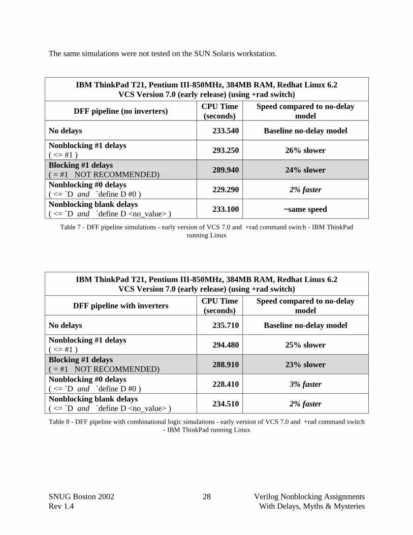
The same simulations were not tested on the SUN Solaris workstation.
IBM ThinkPad T21, Pentium III-850MHz, 384MB RAM, Redhat Linux 6.2VCS Version 7.0 (early release) (using +rad switch)
DFF pipeline (no inverters)CPU Time(seconds)
Speed compared to no-delaymodel
No delays 233.540 Baseline no-delay model
Nonblocking #1 delays( <= #1 )
293.250 26% slower
Blocking #1 delays( = #1 NOT RECOMMENDED)
289.940 24% slower
Nonblocking #0 delays( <= `D and `define D #0 )
229.290 2% faster
Nonblocking blank delays( <= `D and `define D <no_value> )
233.100 ~same speed
Table 7 - DFF pipeline simulations - early version of VCS 7.0 and +rad command switch - IBM ThinkPadrunning Linux
IBM ThinkPad T21, Pentium III-850MHz, 384MB RAM, Redhat Linux 6.2VCS Version 7.0 (early release) (using +rad switch)
DFF pipeline with invertersCPU Time(seconds)
Speed compared to no-delaymodel
No delays 235.710 Baseline no-delay model
Nonblocking #1 delays( <= #1 )
294.480 25% slower
Blocking #1 delays( = #1 NOT RECOMMENDED)
288.910 23% slower
Nonblocking #0 delays( <= `D and `define D #0 )
228.410 3% faster
Nonblocking blank delays( <= `D and `define D <no_value> )
234.510 2% faster
Table 8 - DFF pipeline with combinational logic simulations - early version of VCS 7.0 and +rad command switch- IBM ThinkPad running Linux
SNUG Boston 2002 Verilog Nonblocking AssignmentsRev 1.4 With Delays, Myths & Mysteries
29
9.0 Multiple common clocks and race conditions?
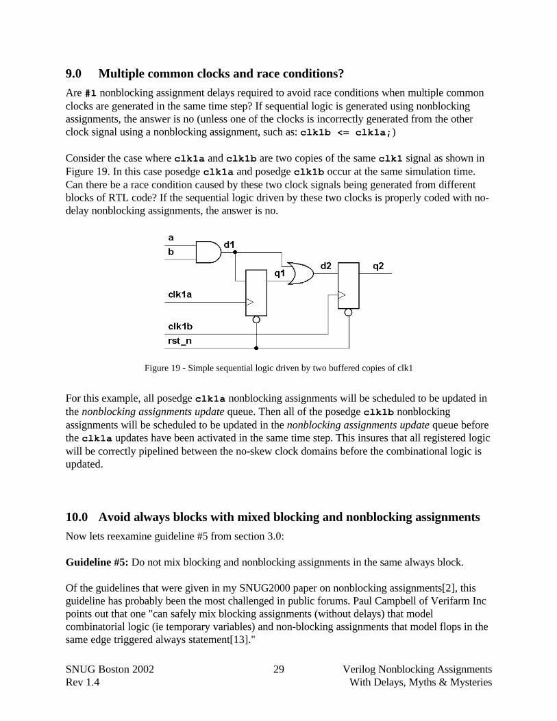
Are #1 nonblocking assignment delays required to avoid race conditions when multiple commonclocks are generated in the same time step? If sequential logic is generated using nonblockingassignments, the answer is no (unless one of the clocks is incorrectly generated from the otherclock signal using a nonblocking assignment, such as: clk1b <= clk1a;)
Consider the case where clk1a and clk1b are two copies of the same clk1 signal as shown inFigure 19. In this case posedge clk1a and posedge clk1b occur at the same simulation time.Can there be a race condition caused by these two clock signals being generated from differentblocks of RTL code? If the sequential logic driven by these two clocks is properly coded with no-delay nonblocking assignments, the answer is no.
Figure 19 - Simple sequential logic driven by two buffered copies of clk1
For this example, all posedge clk1a nonblocking assignments will be scheduled to be updated inthe nonblocking assignments update queue. Then all of the posedge clk1b nonblockingassignments will be scheduled to be updated in the nonblocking assignments update queue beforethe clk1a updates have been activated in the same time step. This insures that all registered logicwill be correctly pipelined between the no-skew clock domains before the combinational logic isupdated.
10.0 Avoid always blocks with mixed blocking and nonblocking assignments
Now lets reexamine guideline #5 from section 3.0:
Guideline #5: Do not mix blocking and nonblocking assignments in the same always block.
Of the guidelines that were given in my SNUG2000 paper on nonblocking assignments[2], thisguideline has probably been the most challenged in public forums. Paul Campbell of Verifarm Incpoints out that one "can safely mix blocking assignments (without delays) that modelcombinatorial logic (ie temporary variables) and non-blocking assignments that model flops in thesame edge triggered always statement[13]."
SNUG Boston 2002 Verilog Nonblocking AssignmentsRev 1.4 With Delays, Myths & Mysteries
30
Paul is of course correct, but the coding style has its disadvantages, including:
1. It can be confusing to understand the event scheduling in this always block.2. One might forget that only one nonblocking assignment should be used and that the
nonblocking assignment should be listed last.3. In a zero delay model, inputs and their resultant flip-flop outputs will change on the same
clock edge yielding a confusing simulation waveform display.
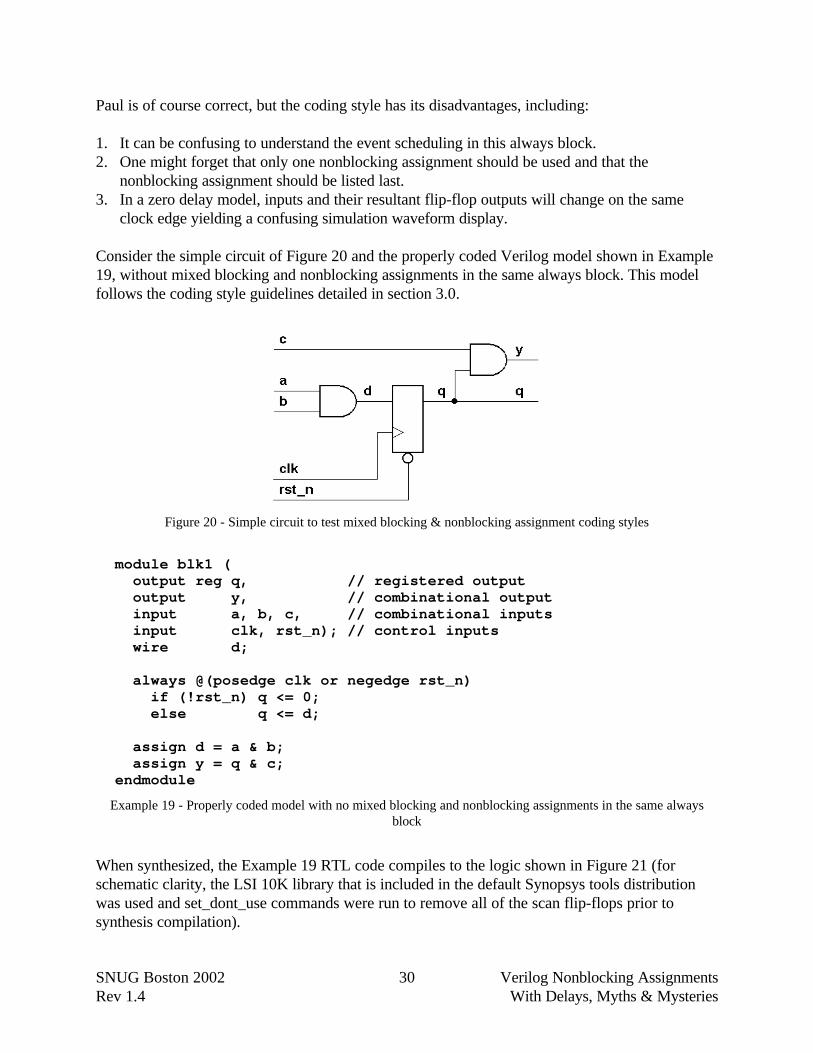
Consider the simple circuit of Figure 20 and the properly coded Verilog model shown in Example19, without mixed blocking and nonblocking assignments in the same always block. This modelfollows the coding style guidelines detailed in section 3.0.
Figure 20 - Simple circuit to test mixed blocking & nonblocking assignment coding styles
module blk1 ( output reg q, // registered output output y, // combinational output input a, b, c, // combinational inputs input clk, rst_n); // control inputs wire d;
always @(posedge clk or negedge rst_n) if (!rst_n) q <= 0; else q <= d;
assign d = a & b; assign y = q & c;endmodule
Example 19 - Properly coded model with no mixed blocking and nonblocking assignments in the same alwaysblock
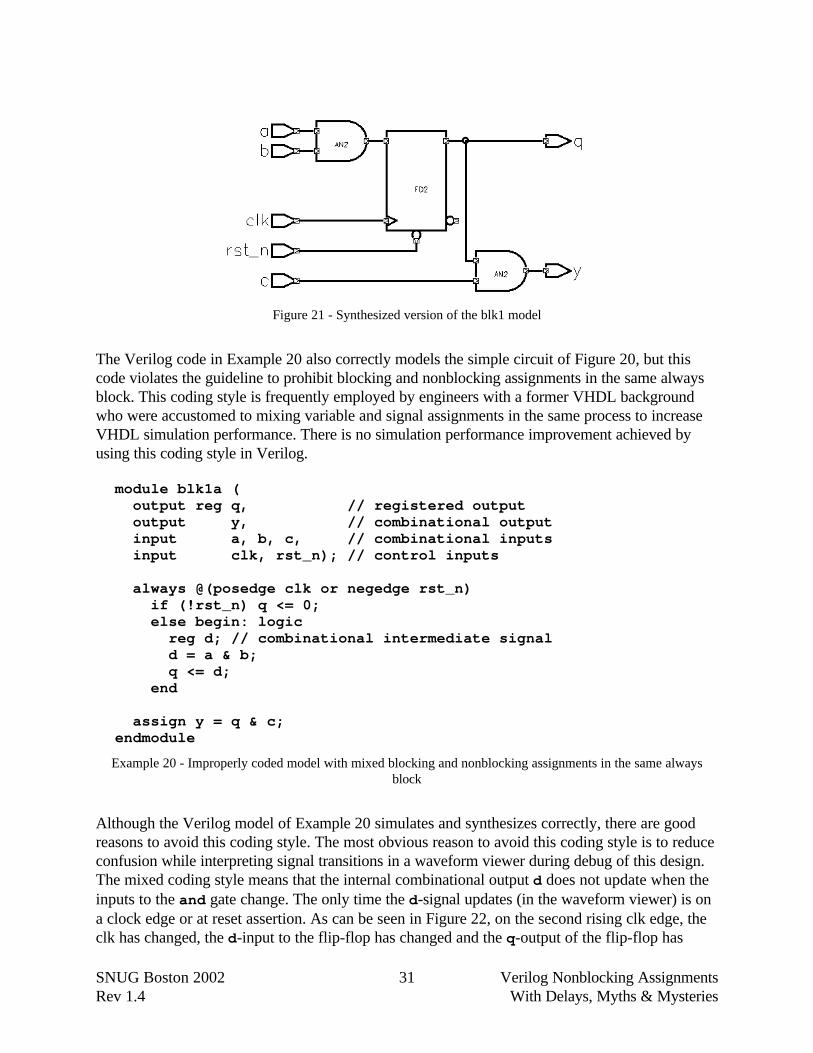
When synthesized, the Example 19 RTL code compiles to the logic shown in Figure 21 (forschematic clarity, the LSI 10K library that is included in the default Synopsys tools distributionwas used and set_dont_use commands were run to remove all of the scan flip-flops prior tosynthesis compilation).
SNUG Boston 2002 Verilog Nonblocking AssignmentsRev 1.4 With Delays, Myths & Mysteries
31
Figure 21 - Synthesized version of the blk1 model
The Verilog code in Example 20 also correctly models the simple circuit of Figure 20, but thiscode violates the guideline to prohibit blocking and nonblocking assignments in the same alwaysblock. This coding style is frequently employed by engineers with a former VHDL backgroundwho were accustomed to mixing variable and signal assignments in the same process to increaseVHDL simulation performance. There is no simulation performance improvement achieved byusing this coding style in Verilog.
module blk1a ( output reg q, // registered output output y, // combinational output input a, b, c, // combinational inputs input clk, rst_n); // control inputs
always @(posedge clk or negedge rst_n) if (!rst_n) q <= 0; else begin: logic reg d; // combinational intermediate signal d = a & b; q <= d; end
assign y = q & c;endmodule
Example 20 - Improperly coded model with mixed blocking and nonblocking assignments in the same alwaysblock
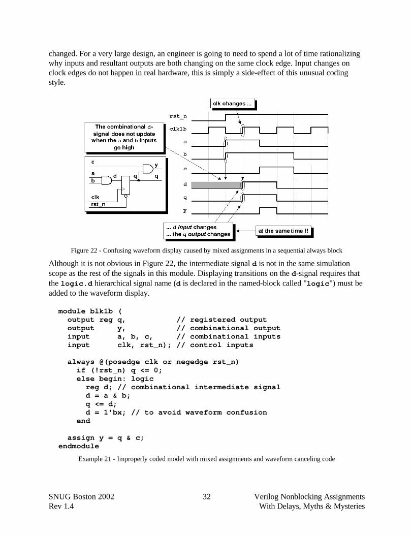
Although the Verilog model of Example 20 simulates and synthesizes correctly, there are goodreasons to avoid this coding style. The most obvious reason to avoid this coding style is to reduceconfusion while interpreting signal transitions in a waveform viewer during debug of this design.The mixed coding style means that the internal combinational output d does not update when theinputs to the and gate change. The only time the d-signal updates (in the waveform viewer) is ona clock edge or at reset assertion. As can be seen in Figure 22, on the second rising clk edge, theclk has changed, the d-input to the flip-flop has changed and the q-output of the flip-flop has
SNUG Boston 2002 Verilog Nonblocking AssignmentsRev 1.4 With Delays, Myths & Mysteries
32
changed. For a very large design, an engineer is going to need to spend a lot of time rationalizingwhy inputs and resultant outputs are both changing on the same clock edge. Input changes onclock edges do not happen in real hardware, this is simply a side-effect of this unusual codingstyle.
Figure 22 - Confusing waveform display caused by mixed assignments in a sequential always block
Although it is not obvious in Figure 22, the intermediate signal d is not in the same simulationscope as the rest of the signals in this module. Displaying transitions on the d-signal requires thatthe logic.d hierarchical signal name (d is declared in the named-block called "logic") must beadded to the waveform display.
module blk1b ( output reg q, // registered output output y, // combinational output input a, b, c, // combinational inputs input clk, rst_n); // control inputs
always @(posedge clk or negedge rst_n) if (!rst_n) q <= 0; else begin: logic reg d; // combinational intermediate signal d = a & b; q <= d; d = 1'bx; // to avoid waveform confusion end
assign y = q & c;endmodule
Example 21 - Improperly coded model with mixed assignments and waveform canceling code
SNUG Boston 2002 Verilog Nonblocking AssignmentsRev 1.4 With Delays, Myths & Mysteries
33
I have been told of one engineer who codes with a mixed assignment style that includes assigningX's to all of the intermediate local signals after making the nonblocking assignment, just to makesure nobody can display the intermediate signals in a waveform display and become confused! Thehighly unusual coding style is shown in Example 21. In this coding style, the intermediate signalsare displayed as unknowns for the entire simulation, even though they took on momentary valuesto update the appropriate sequential logic. This seems like a lot of trouble just to use the mixedcoding style.
Upon examination, I believe the coding style of mixing blocking and nonblocking assignments inthe same always block will not simulate any faster, is not quite as understandable (requires abetter understanding of Verilog event scheduling) and is no easier to code (more opportunities toincorrectly mix blocking and nonblocking assignments and quite confusing in a simulationwaveform display). Even though the mixed style can work, I consider the mixed style to be moreerror prone for coding and for waveform interpretation. Since the coding style offers no distinctadvantage over other recommended coding styles, I stand by the guideline to not mix blockingand nonblocking assignments in the same always block.
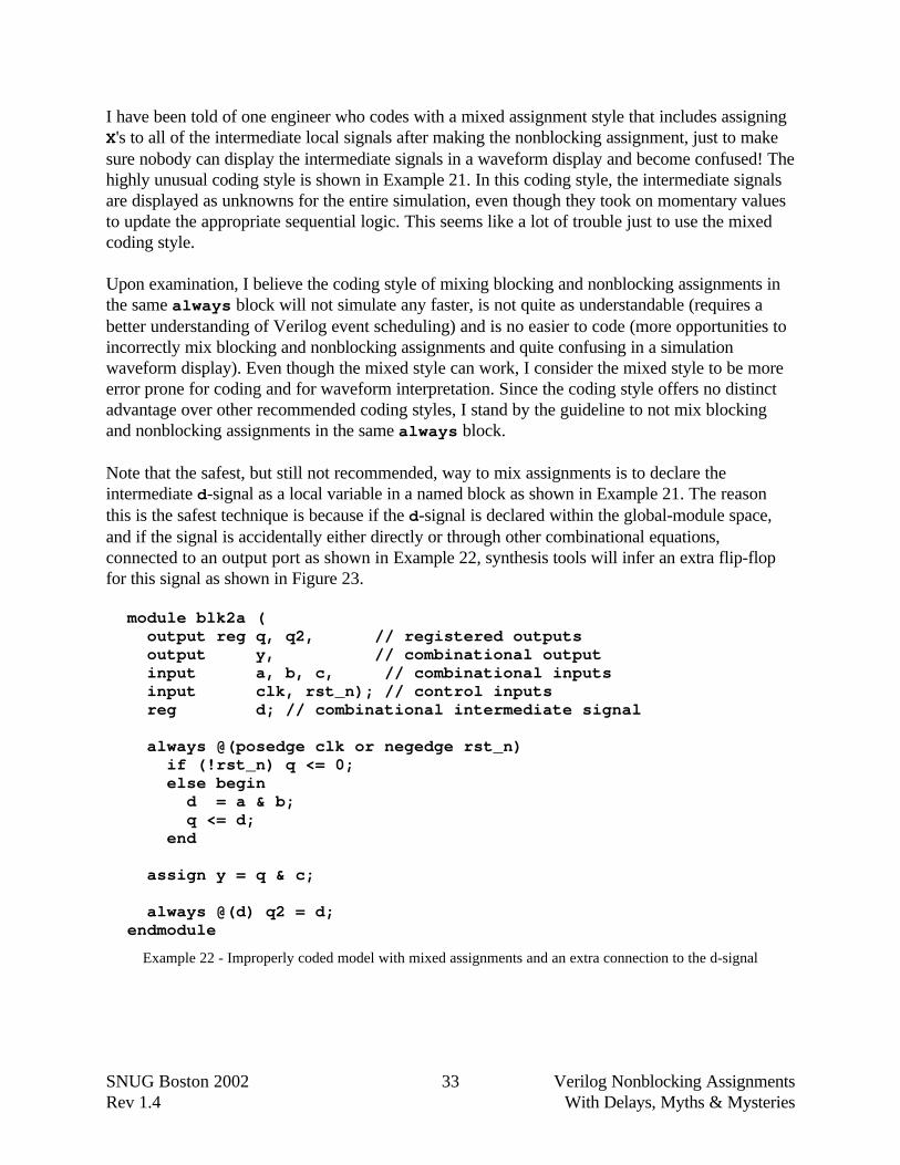
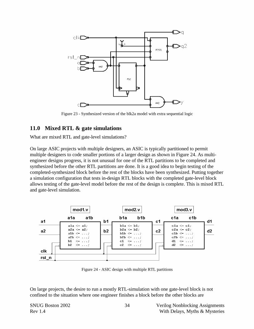
Note that the safest, but still not recommended, way to mix assignments is to declare theintermediate d-signal as a local variable in a named block as shown in Example 21. The reasonthis is the safest technique is because if the d-signal is declared within the global-module space,and if the signal is accidentally either directly or through other combinational equations,connected to an output port as shown in Example 22, synthesis tools will infer an extra flip-flopfor this signal as shown in Figure 23.
module blk2a ( output reg q, q2, // registered outputs output y, // combinational output input a, b, c, // combinational inputs input clk, rst_n); // control inputs reg d; // combinational intermediate signal
always @(posedge clk or negedge rst_n) if (!rst_n) q <= 0; else begin d = a & b; q <= d; end
assign y = q & c;
always @(d) q2 = d;endmodule
Example 22 - Improperly coded model with mixed assignments and an extra connection to the d-signal
SNUG Boston 2002 Verilog Nonblocking AssignmentsRev 1.4 With Delays, Myths & Mysteries
34
Figure 23 - Synthesized version of the blk2a model with extra sequential logic
11.0 Mixed RTL & gate simulations
What are mixed RTL and gate-level simulations?
On large ASIC projects with multiple designers, an ASIC is typically partitioned to permitmultiple designers to code smaller portions of a larger design as shown in Figure 24. As multi-engineer designs progress, it is not unusual for one of the RTL partitions to be completed andsynthesized before the other RTL partitions are done. It is a good idea to begin testing of thecompleted-synthesized block before the rest of the blocks have been synthesized. Putting togethera simulation configuration that tests in-design RTL blocks with the completed gate-level blockallows testing of the gate-level model before the rest of the design is complete. This is mixed RTLand gate-level simulation.
Figure 24 - ASIC design with multiple RTL partitions
On large projects, the desire to run a mostly RTL-simulation with one gate-level block is notconfined to the situation where one engineer finishes a block before the other blocks are
SNUG Boston 2002 Verilog Nonblocking AssignmentsRev 1.4 With Delays, Myths & Mysteries
35
synthesized; indeed, mixed simulations are often run to test a gate-level block in isolation fromother gate-level blocks in a design. This helps to narrow the focus of any potential debuggingeffort and also, because RTL models generally simulate much faster than equivalent gate-levelmodels, using fewer gate-level models will generally improve simulation efficiency.
The question is, are there any problems related to mixed RTL and gate-level simulation?
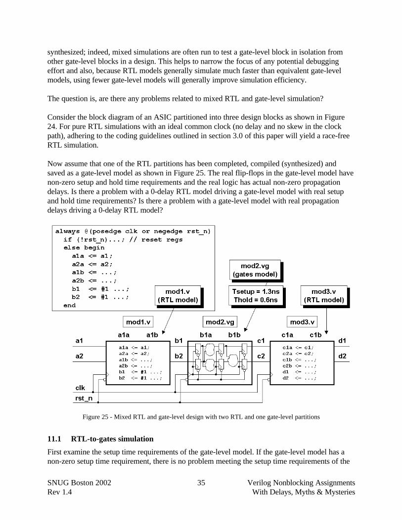
Consider the block diagram of an ASIC partitioned into three design blocks as shown in Figure24. For pure RTL simulations with an ideal common clock (no delay and no skew in the clockpath), adhering to the coding guidelines outlined in section 3.0 of this paper will yield a race-freeRTL simulation.
Now assume that one of the RTL partitions has been completed, compiled (synthesized) andsaved as a gate-level model as shown in Figure 25. The real flip-flops in the gate-level model havenon-zero setup and hold time requirements and the real logic has actual non-zero propagationdelays. Is there a problem with a 0-delay RTL model driving a gate-level model with real setupand hold time requirements? Is there a problem with a gate-level model with real propagationdelays driving a 0-delay RTL model?
Figure 25 - Mixed RTL and gate-level design with two RTL and one gate-level partitions
11.1 RTL-to-gates simulation
First examine the setup time requirements of the gate-level model. If the gate-level model has anon-zero setup time requirement, there is no problem meeting the setup time requirements of the
SNUG Boston 2002 Verilog Nonblocking AssignmentsRev 1.4 With Delays, Myths & Mysteries
36
model when driven by a 0-delay RTL model. As soon as there is a rising clock edge, the RTLmodel immediately changes the outputs that are being driven to the gate-level model so theoutputs are available for a full clock cycle before they must be clocked into the gate-level model.Conclusion: RTL-to-gates: no setup time problems.
Second, examine the hold time requirements of the gate-level model. If the gate-level model has anon-zero hold time requirement, there is a problem meeting the hold time requirements of themodel when driven by a 0-delay RTL model. Again, as soon as there is a rising clock edge, theRTL model immediately changes the outputs that are being driven to the gate-level model, but thegate-level model expected the old data value to be held to meet the hold time requirements of thegate-level model. The RTL model changed the gate-level inputs in zero-time, violating the holdtime requirement of the gate-level model.Conclusion: RTL-to-gates: there are hold time problems.
How can we fix the RTL-to-gates hold time problem? First, recognize that hold times for mostcontemporary high-performance ASIC and FPGA families are generally less than 1ns (typicalnumbers are 0ns to 0.8ns). By adding #1 delays to the outputs of the RTL model, the RTL modelwill hold the pre-clock output values for 1ns, effectively creating a clk-to-q delay that will meetmost ASIC and FPGA hold time requirements.
Will #1 RTL delays fix all RTL-to-gates hold time problems? No. If the gate-level model has holdtimes that are greater than 1ns, the #1 RTL delays will be insufficient to meet the required holdtimes. One common example of a model that may have hold time requirements that exceed 1ns isan instantiated RAM model. It is not unusual for RAM models and other instantiated devices tohave input hold times that are greater than 1ns. For these instantiated models, and indeed for anyinterface between modules, an engineer needs to document the hold time requirements for allinputs and specially note any input hold time that is greater than 1ns. RTL models that driveinputs with longer hold time requirements will need to increase the #1 delays to exceed the holdtime delays of the more critical inputs. Adding a #2 to specific RTL outputs will insure that thoseoutputs will hold their old values for 2ns after a posedge clk.
Since most device hold times are less than 1ns, an engineer who has heretofore ignorantly added#1 delays to all nonblocking assignments, has been lucky and has been able to do mixed RTL andgate-level simulation unaware that potential hold time problems could have caused simulationfailures.
Note that the nonblocking assignment with #1 delay is really the same idea as the delay linemodels of section 6.0 with very short transport delays.
11.2 Gates-to-RTL simulation
When investigating gates-to-RTL simulations, first note that the RTL model being driven by agate-level model has no setup or hold time requirements.
Are there any setup time problems involved in doing a gates-to-RTL simulation? After an activeclock edge, as long as the propagation of data from the gates model to the RTL model happens
SNUG Boston 2002 Verilog Nonblocking AssignmentsRev 1.4 With Delays, Myths & Mysteries
37
within one clock period, there is no setup time violation problem. If the propagation time of thedata from the gates model to the RTL model exceeds one clock period, there is a real designproblem (design does not meet timing) that must be fixed, and not a simulation problem.Conclusion: gates-to-RTL: no simulation-related setup time problems.
Are there any hold time problems involved in doing a gates-to-RTL simulation? After an activeclock edge, even an ultra fast gate-level design has some propagation delay and since the RTLmodel has no hold time requirement, there will be no hold time violation problems in thesimulation.Conclusion: gates-to-RTL: no hold time problems.
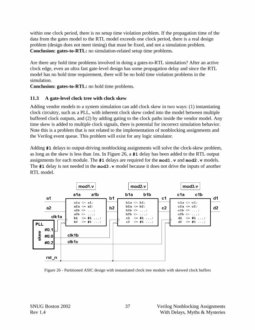
11.3 A gate-level clock tree with clock skew
Adding vendor models to a system simulation can add clock skew in two ways: (1) instantiatingclock circuitry, such as a PLL, with inherent clock skew coded into the model between multiplebuffered clock outputs, and (2) by adding gating to the clock paths inside the vendor model. Anytime skew is added to multiple clock signals, there is potential for incorrect simulation behavior.Note this is a problem that is not related to the implementation of nonblocking assignments andthe Verilog event queue. This problem will exist for any logic simulator.
Adding #1 delays to output-driving nonblocking assignments will solve the clock-skew problem,as long as the skew is less than 1ns. In Figure 26, a #1 delay has been added to the RTL outputassignments for each module. The #1 delays are required for the mod1.v and mod2.v models.The #1 delay is not needed in the mod3.v model because it does not drive the inputs of anotherRTL model.
Figure 26 - Partitioned ASIC design with instantiated clock tree module with skewed clock buffers
SNUG Boston 2002 Verilog Nonblocking AssignmentsRev 1.4 With Delays, Myths & Mysteries
38
11.4 Vendor models with clock skew
If a vendor provides a Verilog model, either as a behavioral model with delays or as a gate-levelmodel with delays, the vendor may have introduced gating or skew into the clock path that couldcause mixed RTL and vendor-model simulations to fail.
Just as was the case with the instantiated clock-tree module with skewed clock buffers of section11.3, as long as the clock-gating or clock-path delays are shorter than 1ns, the mixed-modelsimulation problem can be fixed by making sure that the outputs of the RTL model that drives thevendor model has been coded using nonblocking assignments with #1 delays. If the clock-gatingor clock path delays exceed 1ns, it follows that the driving RTL model will require nonblockingassignment delays to match the longest clock-path delay.
Regardless of the implemented simulation solution, frequent nasty complaints and vicious legalthreats should be sent to any vendor that does not provide the ability to enable ideal, non-gatedclock nets inside their models, or in the case of vendors that provide clock-tree circuitry, such asPLL models, the ability to disable all clock skew between multiply driven clock sources.
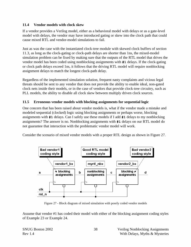
11.5 Erroneous vendor models with blocking assignments for sequential logic
One concern that has been raised about vendor models is, what if the vendor made a mistake andmodeled sequential (clocked) logic using blocking assignments or perhaps worse, blockingassignments with #1 delays. Can I safely use these models if I add #1 delays to my nonblockingassignments? The answer is no. Nonblocking assignments with #1 delays on our RTL model donot guarantee that interaction with the problematic vendor model will work.
Consider the scenario of mixed vendor models with a proper RTL design as shown in Figure 27.
Figure 27 - Block diagram of mixed simulation with poorly coded vendor models
Assume that vendor #1 has coded their model with either of the blocking assignment coding stylesof Example 23 or Example 24.
SNUG Boston 2002 Verilog Nonblocking AssignmentsRev 1.4 With Delays, Myths & Mysteries
39
module vendor1_b0 ( output reg b, input a, clk, rst_n);
always @(posedge clk or negedge rst_n) if (!rst_n) b = 0; else b = a;endmodule
Example 23 - Bad vendor #1 model - blocking assignments with no delays
`timescale 1ns / 1nsmodule vendor1_b1 ( output reg b, input a, clk, rst_n);
always @(posedge clk or negedge rst_n) if (!rst_n) b = #1 0; else b = #1 a;endmodule
Example 24 - Bad vendor #1 model - blocking assignments with #1 delays
Further assume that our RTL design has been properly coded with one of the nonblockingassignment coding styles shown in Example 25 or Example 26.
module myrtl_nb0 ( output reg c, input b, clk, rst_n);
always @(posedge clk or negedge rst_n) if (!rst_n) c <= 0; else c <= b;endmodule
Example 25 - Good RTL model - nonblocking assignments with no delays
`timescale 1ns / 1nsmodule myrtl_nb1 ( output reg c, input b, clk, rst_n);
always @(posedge clk or negedge rst_n) if (!rst_n) c <= #1 0; else c <= #1 b;endmodule
Example 26 - Good RTL model - nonblocking assignments with #1 delays
SNUG Boston 2002 Verilog Nonblocking AssignmentsRev 1.4 With Delays, Myths & Mysteries
40
And finally assume that vendor #2 has coded their model with either of the blocking assignmentcoding styles of Example 27 or Example 28.
module vendor2_b0 ( output reg d, input c, clk, rst_n);
always @(posedge clk or negedge rst_n) if (!rst_n) d = 0; else d = c;endmodule
Example 27 - Bad vendor #2 model - blocking assignments with no delays
`timescale 1ns / 1nsmodule vendor2_b1 ( output reg d, input c, clk, rst_n);
always @(posedge clk or negedge rst_n) if (!rst_n) d = #1 0; else d = #1 c;endmodule
Example 28 - Bad vendor #2 model - blocking assignments with #1 delays
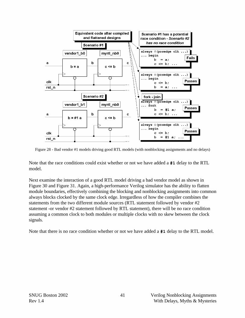
First examine the interaction of a bad vendor model driving the good RTL model. A high-performance Verilog simulator, like VCS, has the ability to flatten module boundaries, effectivelycombining the blocking and nonblocking assignments into common always blocks clocked by thesame clock edge. Depending on how the compiler combines the statements from the two differentmodule sources (vendor #1 statement followed by RTL statement -or- RTL statement followedby vendor #1 statement), there may or may not exist a simulation race condition as shown inFigure 28 and Figure 29.
SNUG Boston 2002 Verilog Nonblocking AssignmentsRev 1.4 With Delays, Myths & Mysteries
41
Figure 28 - Bad vendor #1 models driving good RTL models (with nonblocking assignments and no delays)
Note that the race conditions could exist whether or not we have added a #1 delay to the RTLmodel.
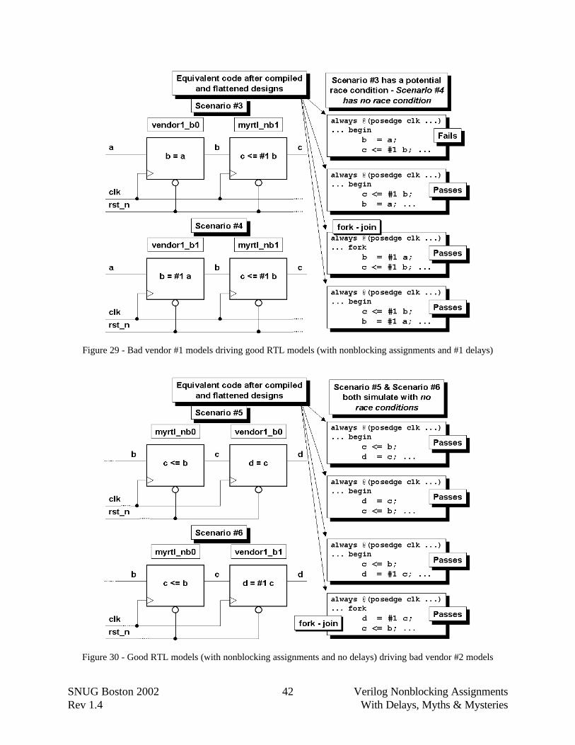
Next examine the interaction of a good RTL model driving a bad vendor model as shown inFigure 30 and Figure 31. Again, a high-performance Verilog simulator has the ability to flattenmodule boundaries, effectively combining the blocking and nonblocking assignments into commonalways blocks clocked by the same clock edge. Irregardless of how the compiler combines thestatements from the two different module sources (RTL statement followed by vendor #2statement -or vendor #2 statement followed by RTL statement), there will be no race conditionassuming a common clock to both modules or multiple clocks with no skew between the clocksignals.
Note that there is no race condition whether or not we have added a #1 delay to the RTL model.
SNUG Boston 2002 Verilog Nonblocking AssignmentsRev 1.4 With Delays, Myths & Mysteries
42
Figure 29 - Bad vendor #1 models driving good RTL models (with nonblocking assignments and #1 delays)
Figure 30 - Good RTL models (with nonblocking assignments and no delays) driving bad vendor #2 models
SNUG Boston 2002 Verilog Nonblocking AssignmentsRev 1.4 With Delays, Myths & Mysteries
43
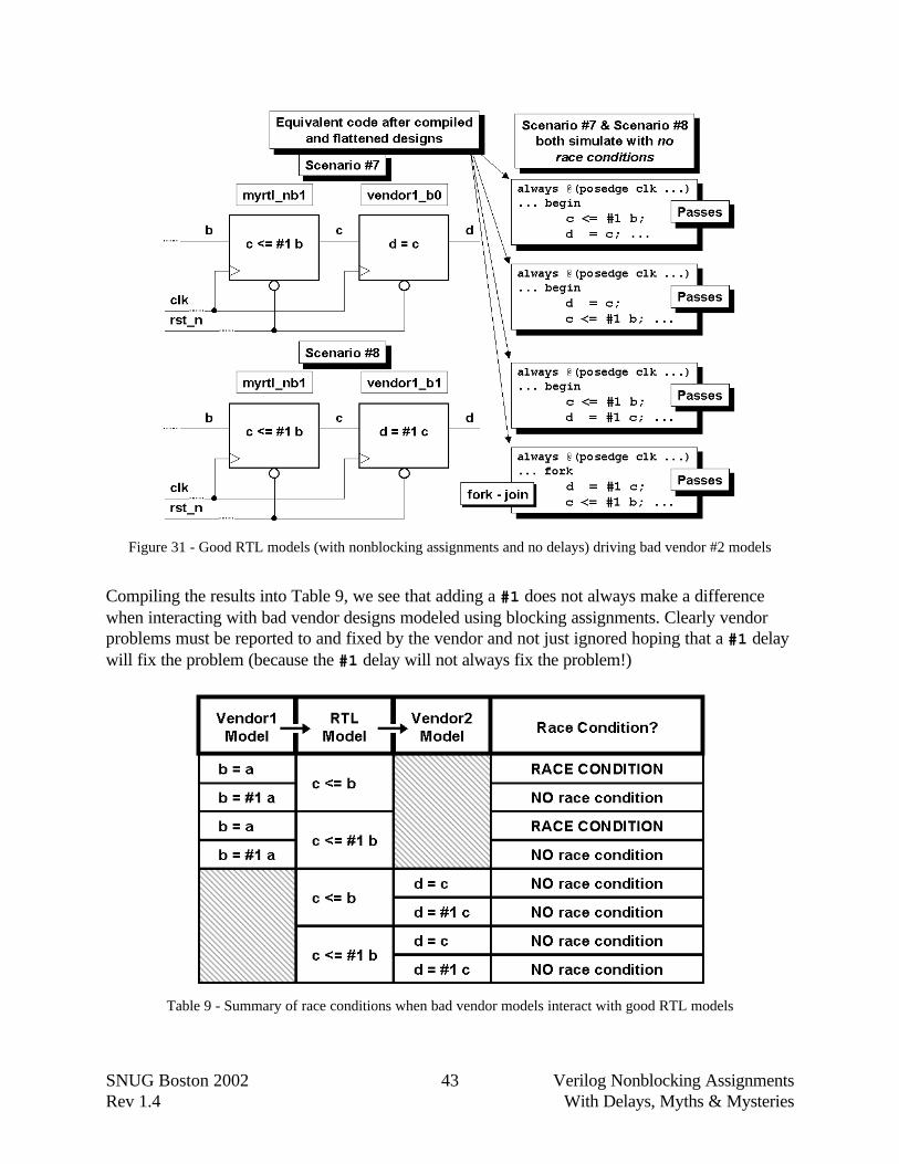
Figure 31 - Good RTL models (with nonblocking assignments and no delays) driving bad vendor #2 models
Compiling the results into Table 9, we see that adding a #1 does not always make a differencewhen interacting with bad vendor designs modeled using blocking assignments. Clearly vendorproblems must be reported to and fixed by the vendor and not just ignored hoping that a #1 delaywill fix the problem (because the #1 delay will not always fix the problem!)
Table 9 - Summary of race conditions when bad vendor models interact with good RTL models
SNUG Boston 2002 Verilog Nonblocking AssignmentsRev 1.4 With Delays, Myths & Mysteries
44
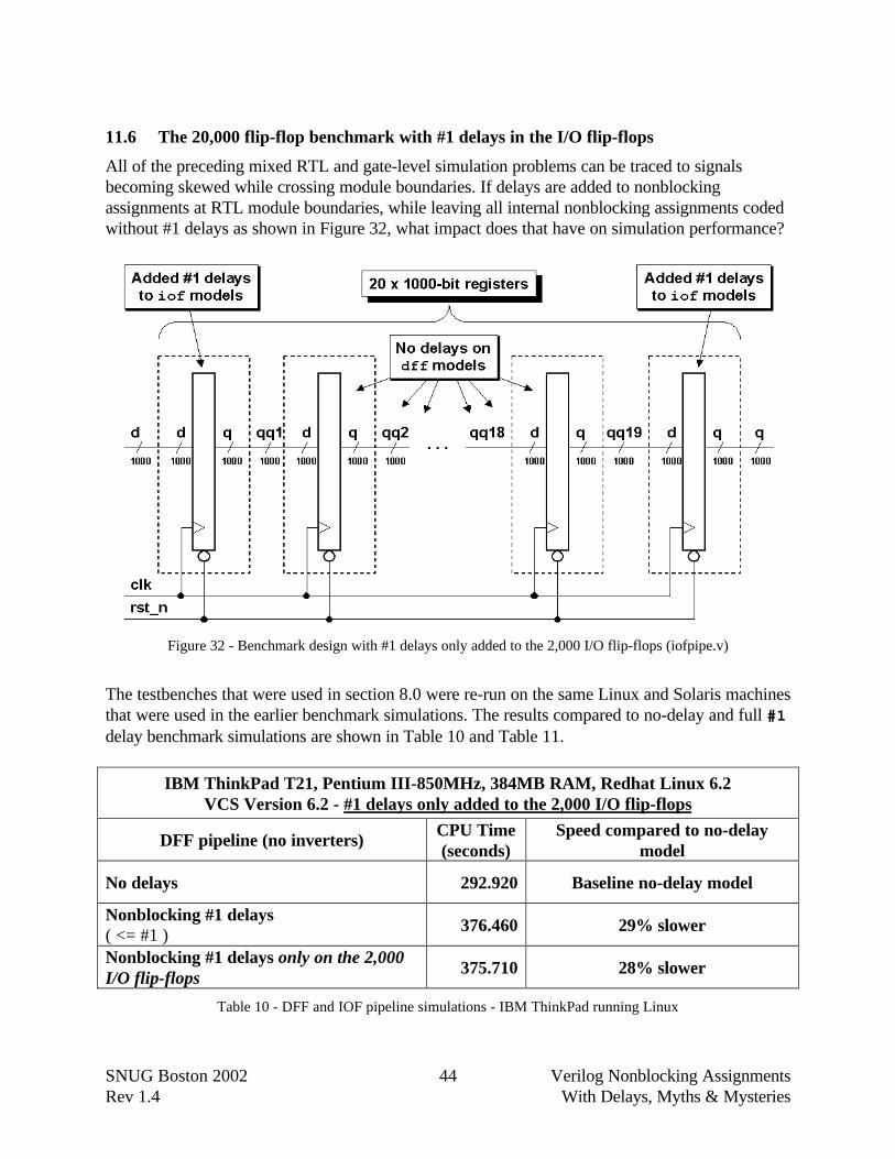
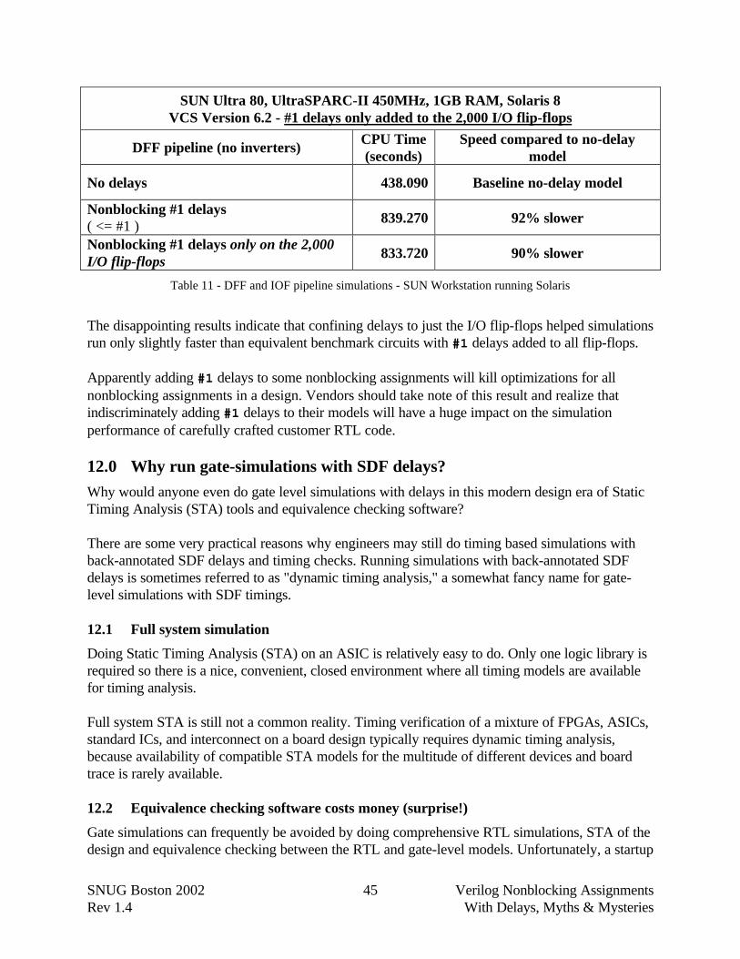
11.6 The 20,000 flip-flop benchmark with #1 delays in the I/O flip-flops
All of the preceding mixed RTL and gate-level simulation problems can be traced to signalsbecoming skewed while crossing module boundaries. If delays are added to nonblockingassignments at RTL module boundaries, while leaving all internal nonblocking assignments codedwithout #1 delays as shown in Figure 32, what impact does that have on simulation performance?
Figure 32 - Benchmark design with #1 delays only added to the 2,000 I/O flip-flops (iofpipe.v)
The testbenches that were used in section 8.0 were re-run on the same Linux and Solaris machinesthat were used in the earlier benchmark simulations. The results compared to no-delay and full #1delay benchmark simulations are shown in Table 10 and Table 11.
IBM ThinkPad T21, Pentium III-850MHz, 384MB RAM, Redhat Linux 6.2VCS Version 6.2 - #1 delays only added to the 2,000 I/O flip-flops
DFF pipeline (no inverters)CPU Time(seconds)
Speed compared to no-delaymodel
No delays 292.920 Baseline no-delay model
Nonblocking #1 delays( <= #1 )
376.460 29% slower
Nonblocking #1 delays only on the 2,000I/O flip-flops
375.710 28% slower
Table 10 - DFF and IOF pipeline simulations - IBM ThinkPad running Linux
SNUG Boston 2002 Verilog Nonblocking AssignmentsRev 1.4 With Delays, Myths & Mysteries
45
SUN Ultra 80, UltraSPARC-II 450MHz, 1GB RAM, Solaris 8VCS Version 6.2 - #1 delays only added to the 2,000 I/O flip-flops
DFF pipeline (no inverters)CPU Time(seconds)
Speed compared to no-delaymodel
No delays 438.090 Baseline no-delay model
Nonblocking #1 delays( <= #1 )
839.270 92% slower
Nonblocking #1 delays only on the 2,000I/O flip-flops
833.720 90% slower
Table 11 - DFF and IOF pipeline simulations - SUN Workstation running Solaris
The disappointing results indicate that confining delays to just the I/O flip-flops helped simulationsrun only slightly faster than equivalent benchmark circuits with #1 delays added to all flip-flops.
Apparently adding #1 delays to some nonblocking assignments will kill optimizations for allnonblocking assignments in a design. Vendors should take note of this result and realize thatindiscriminately adding #1 delays to their models will have a huge impact on the simulationperformance of carefully crafted customer RTL code.
12.0 Why run gate-simulations with SDF delays?
Why would anyone even do gate level simulations with delays in this modern design era of StaticTiming Analysis (STA) tools and equivalence checking software?
There are some very practical reasons why engineers may still do timing based simulations withback-annotated SDF delays and timing checks. Running simulations with back-annotated SDFdelays is sometimes referred to as "dynamic timing analysis," a somewhat fancy name for gate-level simulations with SDF timings.
12.1 Full system simulation
Doing Static Timing Analysis (STA) on an ASIC is relatively easy to do. Only one logic library isrequired so there is a nice, convenient, closed environment where all timing models are availablefor timing analysis.
Full system STA is still not a common reality. Timing verification of a mixture of FPGAs, ASICs,standard ICs, and interconnect on a board design typically requires dynamic timing analysis,because availability of compatible STA models for the multitude of different devices and boardtrace is rarely available.
12.2 Equivalence checking software costs money (surprise!)
Gate simulations can frequently be avoided by doing comprehensive RTL simulations, STA of thedesign and equivalence checking between the RTL and gate-level models. Unfortunately, a startup
SNUG Boston 2002 Verilog Nonblocking AssignmentsRev 1.4 With Delays, Myths & Mysteries
46
or other companies on a tight budget frequently will only have the resources to buy a simulatorand a synthesis tool, such as DesignCompiler. DesignCompiler gives the ability to transform anRTL design into gates and to perform static timing analysis on the design, but in the absence of anequivalency-checking tool, gate-level simulations must be run to verify that the gate-level designmatches the pre-synthesis RTL design.
The second-tier funded design team usually acquires a faster and more comprehensive STA toolin the form of PrimeTime. The third-tier funded company may have the resources to buy anequivalence checking tool such as Formality. Some of the third-tier companies may choosePhysical Compiler before choosing formal verification tools. By the way, all of these companiesalso needed a Verilog simulator (and they're not free either!)
Does that mean that first-tier and second-tier design teams should acknowledge their financial-backing inadequacies and just give up? Obviously, not.
Good methodologies and good coding practices can often minimize the problems that would beidentified by more advanced tools. Companies with limited resources will need to plan carefullyand judiciously partition a design to increase the probability of success so that when the final gate-simulations with SDF timing are performed, the probability of passing all of the simulationvalidation suites will be high; thereby reducing the likelihood that multiple, slow gate-level-simulations with SDF delays will be required.
As a side-note, the upper-tier design teams still may choose tools to accelerate the rapiddeployment of verification environments like VERA or e-Specman before choosing to purchaseequivalence checking tools. So many tools ... so little money!
12.3 Final regression with SDF delays to verify STA and equivalence checked models
An interesting fact is that it still may be useful to run that final gate-simulation with SDF timing toverify that the STA-checked and equivalence-checked design is correct.
A few years ago, one SNUG attendee (identity unknown) reported that out of ten ASIC designshe had worked on, SDF-delay gate-simulations revealed problems not reported by STA tools onnine of the ten designs.
I am not personally aware of the types of problems that are revealed by gate-level simulations thatare not caught by STA and equivalence checking tools. If anyone knows of actual problemscaught by gate-simulations that were missed by STA and equivalence checking tools, please emailyour experiences to [email protected]. I hope to track and publish commonproblems that were found by gate-level simulations, not detected by other tools. Over time, thistracking list may be used to improve other tools.
SNUG Boston 2002 Verilog Nonblocking AssignmentsRev 1.4 With Delays, Myths & Mysteries
47
13.0 Testbench techniques for cycle-based friendly simulation
There are a few simple tricks that can help engineers test their cycle-based RTL designs and avoidcommon Verilog race conditions. Some of these tricks are detailed in this section.
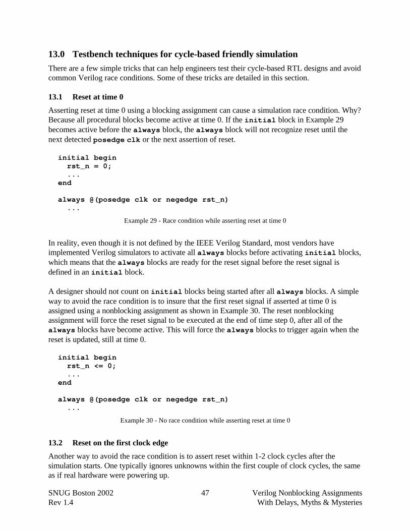
13.1 Reset at time 0
Asserting reset at time 0 using a blocking assignment can cause a simulation race condition. Why?Because all procedural blocks become active at time 0. If the initial block in Example 29becomes active before the always block, the always block will not recognize reset until thenext detected posedge clk or the next assertion of reset.
initial begin rst_n = 0; ...end
always @(posedge clk or negedge rst_n) ...
Example 29 - Race condition while asserting reset at time 0
In reality, even though it is not defined by the IEEE Verilog Standard, most vendors haveimplemented Verilog simulators to activate all always blocks before activating initial blocks,which means that the always blocks are ready for the reset signal before the reset signal isdefined in an initial block.
A designer should not count on initial blocks being started after all always blocks. A simpleway to avoid the race condition is to insure that the first reset signal if asserted at time 0 isassigned using a nonblocking assignment as shown in Example 30. The reset nonblockingassignment will force the reset signal to be executed at the end of time step 0, after all of thealways blocks have become active. This will force the always blocks to trigger again when thereset is updated, still at time 0.
initial begin rst_n <= 0; ...end
always @(posedge clk or negedge rst_n) ...
Example 30 - No race condition while asserting reset at time 0
13.2 Reset on the first clock edge
Another way to avoid the race condition is to assert reset within 1-2 clock cycles after thesimulation starts. One typically ignores unknowns within the first couple of clock cycles, the sameas if real hardware were powering up.
SNUG Boston 2002 Verilog Nonblocking AssignmentsRev 1.4 With Delays, Myths & Mysteries
48
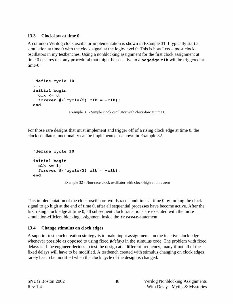
13.3 Clock-low at time 0
A common Verilog clock oscillator implementation is shown in Example 31. I typically start asimulation at time 0 with the clock signal at the logic-level 0. This is how I code most clockoscillators in my testbenches. Using a nonblocking assignment for the first clock assignment attime 0 ensures that any procedural that might be sensitive to a negedge clk will be triggered attime-0.
`define cycle 10...initial begin clk <= 0; forever #(`cycle/2) clk = ~clk);end
Example 31 - Simple clock oscillator with clock-low at time 0
For those rare designs that must implement and trigger off of a rising clock edge at time 0, theclock oscillator functionality can be implemented as shown in Example 32.
`define cycle 10...initial begin clk <= 1; forever #(`cycle/2) clk = ~clk);end
Example 32 - Non-race clock oscillator with clock-high at time zero
This implementation of the clock oscillator avoids race conditions at time 0 by forcing the clocksignal to go high at the end of time 0, after all sequential processes have become active. After thefirst rising clock edge at time 0, all subsequent clock transitions are executed with the moresimulation-efficient blocking assignment inside the forever-statement.
13.4 Change stimulus on clock edges
A superior testbench creation strategy is to make input assignments on the inactive clock edgewhenever possible as opposed to using fixed #delays in the stimulus code. The problem with fixeddelays is if the engineer decides to test the design at a different frequency, many if not all of thefixed delays will have to be modified. A testbench created with stimulus changing on clock edgesrarely has to be modified when the clock cycle of the design is changed.

SNUG Boston 2002 Verilog Nonblocking AssignmentsRev 1.4 With Delays, Myths & Mysteries
49
14.0 Problems with the Bergeron race-avoidance guidelines
Janick Bergeron has written a fine book on writing testbenches, but I find myself in strongdisagreement with some of the guidelines he shares in his book. Bergeron gives the following four"Guidelines for Avoiding Race Conditions:[10]"
1. If a register is declared outside of the always or initial block, assign to it using a nonblockingassignment. Reserve the blocking assignment for registers local to the block.
2. Assign to a register from a single always or initial block.3. Use continuous assignments to drive inout pins only. Do not use them to model internal
conbinational functions. Prefer sequential code instead.4. Do not assign any value at time 0.
Of these guidelines, I disagree with guidelines 1, 3 and 4, and I believe guideline 2 is understated.
With reference to Bergeron guideline #1: As detailed in section 10.0, I see no compelling reasonto mix blocking and nonblocking assignments in the same always block. I do not believe thisguideline makes simulations significantly faster, the coding style more understandable (in fact Ibelieve this coding style requires a more in-depth understanding of the Verilog event queue tounderstand why this works) and adherence to this guideline does not make the functionality easierto code. Note the internally declared variable is visible to simulation waveforms at a lower level ofhierarchy, which reduces design observability. Even if the declaration is moved outside of thealways block, the waveform display will show both input and resultant output signals changing onthe same waveform clock edge (very confusing).
With reference to Bergeron guideline #2: I largely agree with this guideline but I would extend itto say:Cummings Guideline #6: Do not make assignments to the same variable from more than onealways block (or from the perspective of a testbench, from more than one initial block).
With reference to Bergeron guideline #3: Most simple combinational logic is more easily andmuch more concisely coded using continuous assignments. I typically code a combinationalalways block when I want to use for-loops, case statements or explicit if-else statements. Isometimes code a large combinational always block to show the grouping of a set of closely-coupled equations. I do not believe the Bergeron guideline makes simulations significantly faster,the coding style more understandable or the functionality easier to code (in fact, a combinationalalways block frequently has additional declaration overhead and a more verboseimplementation).
With reference to Bergeron guideline #4: The apparent intent is to avoid race conditions that canoccur at time 0. As shown in section 13.0 this can be easily avoided by making the first resetassignment using a nonblocking assignment and/or making the first clock assignment using anonblocking assignment. I see no reason to leave simulation signals undefined at time 0.
SNUG Boston 2002 Verilog Nonblocking AssignmentsRev 1.4 With Delays, Myths & Mysteries
50
15.0 Conclusions and Recommendations
Bergeron makes the observation that he had "yet to see a single testbench that simulates withidentical results on Verilog-XL and VCS[9]." I believe Bergeron is following the wrongguidelines.
When following the guidelines presented in this paper, except when there have been simulatorbugs, I have yet to see a testbench simulate differently between any two major Verilog simulators.
Adding a #1 delay to the RHS of nonblocking assignments can provide some utility, but it alsohas a significant performance cost during the highest performance Verilog simulations. Althoughthe +nbaopt compiler switch described in section 8.2 can improve the performance ofnonblocking assignments with #1 delays, the switch still does not cause #1-delay coded models toachieve quite the same simulation performance as no-delay models.
If an engineer insists on using #1 delays with nonblocking assignments, it would be best to addthe delay as a `D macro definition as described in section 8.1 to still permit simulations withoutdelays that can run up to 100% faster than simulations with #1 delays.
Based on the above observations, I still prefer the simplicity of coding nonblocking assignmentswith no delays. If delays are later required for mixed RTL and gates simulations, I can add therequired nonblocking assignment delays to the outputs of my models (the only place where it isreally required for correct simulation) or I can quickly open my design files and globally substitute/<=/<= `D/ and add the conditional `D macro definition (basically I am lazy and can fix mixedsimulation race problems very easily if necessary). Yes I know that the global substitution willalso introduce syntax errors in the few places where I have used the less-than-or-equal-tooperator (<=) but those are easily detected and corrected syntax errors when the design isrecompiled.
The alternate and equally valid strategy is to add conditional `D macro definitions right from thestart of a project to all RTL models. This strategy will help avoid 90%+ of the potential mixedsimulation problems that might occur in the future. It is also an easy coding guideline to imposeon the less-Verilog-educated masses. Keep in mind that a #1 delay is not always enough to fix allmixed simulation problems.
Using either of the above techniques, it would still be wise to execute a "grep "<= #1" *.v"command to find inefficient assignments that will seriously impact simulator performance. If youare using an operating system that does not support the grep command, you probably havingbigger problems to worry about than simple #1 delay usage!
Vendors must consider the many ways that their IP may be used in simulations with ideal RTLVerilog code. Vendor IP should be modeled either with ideal clock signals (no logic or skewdelays in the clock paths) or permit the selection of an ideal clock signal to facilitate mixed RTLand gate-level simulations. I recommend that an ideal clock network be selectable by either
SNUG Boston 2002 Verilog Nonblocking AssignmentsRev 1.4 With Delays, Myths & Mysteries
51
making the macro definition, `define IDEAL_CLOCK or by turning on the command line macrodefinition +define+IDEAL_CLOCK which is equivalent to the RTL macro definition.
Engineers must understand why delays might be added to nonblocking assignments tocomprehend that a #1 delay may not always be sufficient to fix mixed RTL and gate-levelsimulations. If the clock skew is greater than 1ns or if a gate-level model has an input hold-timerequirement of greater than 1ns, the ignorantly applied #1 delays will not fix the simulationproblem and much unnecessary cussing will ensue! ☺
15.1 Recommended VCS enhancement: +nba1 command switch
Engineers could avoid coding most nonblocking assignment #1 delays if VCS and other leadingsimulator-vendors would implement a +nba1 command line switch to automatically add #1delays to all no-delay nonblocking assignments in sequential always blocks.
The +nba1 switch could assist engineers to easily detect simulation problems related to deficientvendor models, skewed clock delays or mixed RTL and gate-level simulations. This switch wouldprove a valuable debugging tool in large, mixed, system simulation environments.
16.0 Acknowledgements
My thanks to Leah Clark of Cypress Semiconductor and Steve Golson of Trilobyte Systems forreviewing and providing valuable feedback about this paper. And my thanks to Mark Warren,Technical Director of the Verification Technology Group at Synopsys for answering questionsand offering suggestions related to cycle-based simulation and simulation acceleration using VCS.
17.0 References
[1] Adam Krolnik, personal communication.
[2] Clifford E. Cummings, "Nonblocking Assignments in Verilog Synthesis, Coding Styles ThatKill!," SNUG (Synopsys Users Group) 2000 User Papers, section-MC1 (1st paper), March2000. Also available at www.sunburst-design.com/papers
[3] Clifford Cummings, "Correct Methods For Adding Delays To Verilog Behavioral Models,"International HDL Conference 1999 Proceedings, pp. 23-29, April 1999. Also available atwww.sunburst-design.com/papers
[4] IEEE Standard Hardware Description Language Based on the Verilog HardwareDescription Language, IEEE Computer Society, IEEE, New York, NY, IEEE Std 1364-1995
[5] IEEE Standard Verilog Hardware Description Language, IEEE Computer Society, IEEE,New York, NY, IEEE Std 1364-2001.
[6] IEEE P1364.1/D2.1 Draft Standard for Verilog Register Transfer Level Synthesis,http://www.eda.org/vlog-synth/drafts.html
[7] Janick Bergeron, Writing Testbenches, Functional Verification of HDL Models, KluwerAcademic Publishers, 2000.
SNUG Boston 2002 Verilog Nonblocking AssignmentsRev 1.4 With Delays, Myths & Mysteries
52
[8] Janick Bergeron, Writing Testbenches, Functional Verification of HDL Models, KluwerAcademic Publishers, 2000, pg. xxi. (Verilog learning curve)
[9] Janick Bergeron, Writing Testbenches, Functional Verification of HDL Models, KluwerAcademic Publishers, 2000, pg. 140. (Verilog portability exaggeration)
[10] Janick Bergeron, Writing Testbenches, Functional Verification of HDL Models, KluwerAcademic Publishers, 2000, pg. 147. (flawed race avoidance guidelines)
[11] Lionel Bening, and Harry Foster, Principles of Verifiable RTL Design, Second Edition,Kluwer Academic Publishers, 2001
[12] Mark Warren, Technical Director, Verification Technology Group, Synopsys. Personalcommunication.
[13] Paul Campbell, "A note on Verilog® assignments," VeriFarm Inc web site. Downloadedfrom www.verifarm.com/assign.shtml
[14] Steve Golson, personal communication.
[15] Steven Leung, "Subject: Re: How does one do a delay-line model in Verilog," posting oncomp.lang.verilog, 1993-02-12 (found on web site groups.google.com)
Author & Contact Information
Cliff Cummings, President of Sunburst Design, Inc., is an independent EDA consultant and trainerwith 21 years of ASIC, FPGA and system design experience and 11 years of Verilog, synthesisand methodology training experience.
Mr. Cummings has co-authored five Verilog and SystemVerilog books: the 1995 and 2001 IEEEVerilog Standards, the 2002 IEEE Verilog RTL Synthesis Standard and the 2002 AccelleraSystemVerilog Standard. Mr. Cummings is the only Verilog trainer to co-develop all five of thesestandards.
Mr. Cummings holds a BSEE from Brigham Young University and an MSEE from Oregon StateUniversity.
Information about expert Verilog and SystemVerilog training courses offered by Cliff Cummingsof Sunburst Design is available on the www.sunburst-design.com web site.
Email address: [email protected] updated version of this paper can be downloaded from the web site:
www.sunburst-design.com/papers (Data accurate as of May 9th, 2003)
Revision 1.1 (September 2002) - What Changed?
Figure 4 at the end of section 2.1 was replaced with Figure 4 and Figure 5 to show different re-triggered event scheduling caused by blocking assignments or continuous assignments (Figure 4)
SNUG Boston 2002 Verilog Nonblocking AssignmentsRev 1.4 With Delays, Myths & Mysteries
53
and re-triggered event scheduling caused by nonblocking assignments (Figure 5). The two figuresshow different ways that events can be re-triggered in the same simulation time step.
Revision 1.2 (October 2002) - What Changed?
The delay model of Example 5 was corrected to show both y1 and y2 outputs. The PDF was alsocorrected to fix formatting problems that existed on page 5.
Revision 1.3 (December 2002) - What Changed?
Figure 28, Figure 29, Figure 30, Figure 31 and Table 9 were all corrected for the case where ablocking assignment with RHS delay precedes a second assignment. In every case, the behavior isequivalent to making the assignments using fork-join. A RHS #1 delay on a blockingassignment between begin-end delays execution of the second assignment until #1 after the firstassignment has been executed. The correct behavior is to allow the second assignment to startexecution concurrently with the first assignment; hence, the need for the fork-join to replacethe begin-end in these examples. This also means there are fewer race conditions than reportedin earlier versions of this paper, so the table also had to be updated.
Added reference [3] to the references section.
There is actually another good reason to NOT use delays after blocking assignments as shown inExample 24. If rst_n is asserted 0.5 ns after the posedge clk and if the posedge clk isgoing to drive a 1 to the b output, the reset will not be detected until the next posedge clk.
My 1999 HDLCON paper[3] went into detail about adding delays to behavioral models. Oneimportant guideline from that paper was to never put delays on the RHS of blocking assignmentsbecause events can be missed. If you use sequential reset, you can probably get away with addingthe RHS delay, but this is a bad habit to develop and some day you are going to use it wrong andthe debug effort will be painful. It is better not to use this coding style.
Revision 1.4 (May 2003) - What Changed?
All references to "potential race condition" were changed to "race condition" since the potentialfor a race condition really means that a race condition exists in the coding style.
The initial clock assignment in Example 31 was changed from a blocking assignment to anonblocking assignment to ensure that all procedural blocks that might be sensitive to a negedgeclk will be guaranteed to trigger at time-0 with no race condition.
Minor typographical errors were corrected and the author & contact information was alsoupdated.