variability and reliability analysis of cnfet technology ...the percentage of m-cnts is not enough...
TRANSCRIPT

Variability and Reliability Analysis of CNFET
Technology: Impact of Manufacturing Imperfections
Carmen G. Almudever, Antonio Rubio
Department of Electronic Engineering, UPC Barcelona Tech, Barcelona, Spain
Abstract
Carbon nanotube field-effect transistors (CNFETs) are promising candidates
to substitute silicon transistors. Boasting extraordinary electronic properties,
CNFETs exhibit characteristics rivaling those of state-of-the-art Si-based
metal-oxide-semiconductor field-effect transistors (MOSFETs). However, as
any technology that is in development, CNFET fabrication process still have
some imperfections that results in carbon nanotube variations, which can
have a severe impact on the devices’ performance and jeopardize their relia-
bility (in this work the term reliability means time-zero failure due to manu-
facturing variations). This paper presents a study of the effects on transistors
of the main CNFET manufacturing imperfections, including the presence of
metallic carbon nanotubes (m-CNTs), imperfect m-CNT removal processes,
chirality drift, CNT doping variations in the source/drain extension regions,
and density fluctuations due to non-uniform inter-CNT spacing.
Keywords: Carbon nanotubes (CNTs), carbon nanotube field-effect
transistors (CNFETs), CNFET manufacturing imperfections, CNFET
Email addresses: carmen.garcia.almudever@upc (Carmen G. Almudever),[email protected] (Antonio Rubio)
Preprint submitted to Microelectronics Reliability August 30, 2014
“NOTICE: this is the author’s version of a work that was accepted for publication in MICROELECTRONICS RELIABILITYChanges resulting from the publishing process, such as peer review, editing, corrections, structural formatting, and other quality control mechanisms may not be reflected in this document. Changes may have been made to this work since it was submitted for publication. A definitive version was subsequently published in MICROELECTRONICS RELIABILITY Volume 55, Issue 2, February 2015, Pages 358–366 DOI http://dx.doi.org/10.1016/j.microrel.2014.11.011

variability and reliability
1. Introduction
The aggressive scaling down of the physical dimensions of metal-oxide-
semiconductor field-effect transistors (MOSFETs)has required the introduc-
tion of a wide variety of innovative factors to ensure that they are still prop-
erly manufactured. However, with each new generation of MOSFETs, and
the resulting shrinking of the devices’ dimensions to an atomistic scale, the
manufacturing challenges have become more difficult, and statistical variabil-
ity has emerged as a key issue [1]. According to the International Technol-
ogy Roadmap for Semiconductors (ITRS) [2], intensive research is needed to
continue this process and to develop new devices and methods to steer the
technology improvements in other directions.
In recent years, carbon nanotubes (CNTs) have been attracting consid-
erable attention in the field of nanotechnology. They are considered to be a
promising substitute for silicon because of their small size, unusual geometry
(1D structure), and extraordinary electronic properties, including excellent
carrier mobility and quasi-ballistic transport [3], [4].
Carbon nanotube field-effect transistors (CNFETs) could be potential
substitutes for MOSFETs [5], [6]. “Ideal” CNFETs (meaning all CNTs in
the transistor are semiconducting, have the same diameter, and are aligned
and well-positioned) are predicted to be 5x faster than silicon CMOS, while
consuming the same power [7]. However, CNFETs are also affected by man-
ufacturing variability [8], [9], and several significant challenges must be over-
come before these benefits can be achieved. Certain CNFET manufacturing
2

imperfections, such as CNT diameter and doping variations, mispositioned
and misaligned CNTs, the presence of metallic CNTs (m-CNTs), and CNT
density variations, can affect CNFET performance and reliability and must
be addressed. Note that in this work the term reliability refers to failures in
CNFETs because of CNT variations that results from manufacturing imper-
fections (time-zero failures).
In [10] how CNFET manufacturing variations (including CNT diameter
and doping variations, the presence of m-CNTs, and the imperfections of m-
CNT removal processes) affect the radio frequency performance of CNFET
devices and circuits was analyzed. The effects of CNT count variations (CNT
density variations + perfect removal of m-CNTs) on CNFET devices and
digital circuits were studied in our previous publication [11] and in [12],
respectively. In this paper, we will analyze the impact of these and all the
other CNFET manufacturing challenges mentioned above on multi-channel
CNFET variability and reliability in different m-CNT removal scenarios. To
this end, the rest of the paper is organized as follows: Section II reviews
the main imperfections inherent in the CNFET manufacturing process as
well as the main challenges for achieving high-performance CNFETs, Section
III describes the CNFET model and variability analysis methodology using
Monte Carlo simulations, Section IV discusses a CNFET variability study,
Section V presents an analytical CNFET failure model , and Section VI
presents the conclusions.
3
2. Manufacturing imperfections in CNFETs and challenges
As any technology that is in development, CNFET manufacturing process
still have some imperfections, including:
• The alignment and positioning of the CNTs during the CNT growth
process: CNTs grown on quartz substrates can yield nearly perfectly
linear (> 99.9%) aligned arrays of CNTs [13], but there remains a
non-negligible fraction of mispositioned CNTs that can interfere with
the logic functionality. Nevertheless, CNFET circuits immune to such
mispositioned CNTs have been developed [14].
• CNT diameter variations: Chirality is responsible for the CNT diam-
eter. Since the band-gap of CNTs is strongly dependent on diameter,
accurate control of the diameter is essential to the performance of CN-
FETs. Diameter variations cause fluctuations in the CNFET’s thresh-
old voltage and drive current. Typical CNT growth techniques produce
CNTs with diameters ranging from 0.5 to 3nm, but the standard devi-
ation of the CNT diameter can often be controlled within 10% of the
mean diameter [13].
• CNT doping variations: These variations refers to the variations of
the doping concentration in the source/drain extension regions of a
CNFET. It is worth noting that CNFETs, specially n-type CNFETs,
need to be doped to give the transistor its polarity.
• CNT density variations [15], [11]: These variations are due to the
non-uniform spacing between CNTs (non-uniform pitch) during CNT
4

growth, resulting in variations in the number of CNTs in the transis-
tor (CNT count variations). Not only do they cause large variations
in CNFET performance, but they also lead to a significant probability
of complete failure in cases where there are no CNTs present in the
CNFET (opens).
• The presence of metallic CNTs among semiconducting CNTs (s-CNTs):
Metallic CNTs should not be used to make CNFETs because their high
conductivity makes it impossible to control the current with the gate,
thereby causing source-to-drain shorts in the CNFET. In a typical CNT
synthesis process, 1/3 of CNTs are metallic and 2/3 are semiconduct-
ing. In order to reduce the proportion of m-CNTs, different processing
options can be used. One option is to grow predominantly s-CNTs.
Enhanced CNT growth methods can be used to achieve a percentage
of s-CNTs between 90% and 96% [18], [19]. Another alternative is to
separate the m-CNTs from the s-CNTs after the CNT growth to ob-
tain mostly s-CNTs. In this regard, a considerable reduction in the
percentage of m-CNTs (to 1%-5% m-CNTs) has also been achieved
with CNT self-sorting techniques [20]. However, this improvement in
the percentage of m-CNTs is not enough for very-large-scale integration
(VLSI) digital circuits. For high-performance logic applications, which
would require billions of transistors, the impurity concentration of m-
CNTs would need to be less than 0.0001%. A third processing option
is thus to remove the m-CNTs after the CNT growth. Existing tech-
niques for m-CNT removal include single-device electrical breakdown
(SDB) [21], gas-phase and chemical-reaction-based removal techniques
5
[22], and VLSI-compatible metallic-CNT removal (VMR) [23]. SDB re-
moves ∼ 100% of m-CNTs, but it is not VLSI-compatible. Gas-phase
chemical-reaction-based removal techniques are highly compatible with
VLSI semiconductor processing, but m-CNT removal depends on CNT
diameters, and a narrow CNT diameter distribution is required. Fi-
nally, VMR is VLSI-compatible but can impose area penalties. Fur-
thermore, non of all these m-CNT removal techniques is perfect; some
m-CNTs still survive after m-CNT removal, while a non-negligible frac-
tion (typically, 10%-40%) of the s-CNTs can accidentally be eliminated
during the process. As a result, the number of CNTs in the transistor
decreases, thereby increasing the likelihood of failure (opens). A novel
and promising approach for m-CNT removal called thermocapillary-
resist was recently presented in [24]. This technique has been used
to achieve the highly selective of m-CNTs from the full length of an
aligned array of CNTs on a chip without damaging the s-CNTs. How-
ever, it must be improved before it can be used with very high CNT
densities.
It should be noted that all of the above CNT imperfections are typical of
the CVD method. Another approach is to use solution-processed CNTs [25].
With this method, the CNTs are first suspended in solution, and then sepa-
rated, assembled, and deposited onto substrates for device fabrication. This
process offers unique processing advantages over the CVD method, includ-
ing the capabilities of separating nanotubes by electronic type (with s-CNT
purity of over 99%) and depositing them onto various substrates in the form
of ultradensely aligned arrays at low temperature. However, long-channel
6

CNFETs that use solution-processed CNTs generally show inferior device
performance due to the presence of a higher number of structural defects.
In addition, the realization of high-performance CNFETs requires ad-
vances in the following areas:
• Increased CNT density: The most used method for growing CNTs is
chemical vapor deposition (CVD). CNT arrays are grown on a quartz
wafer. They are then transferred onto a target substrate (e.g., a silicon
wafer) for circuit fabrication. The average CNT density obtained today
with this technique is in the range of 1-10 CNTs/µm. Multiple-growth
or multiple-transfer techniques [16], [17] can increase the CNT density
up to 45-55 CNTs/µm. However, that is still significantly lower than
the CNT density required for logic circuits, i.e., 250 CNTs/µm. This
notwithstanding, higher CNT densities (more than 500 CNTs/µm) can
be obtained using other methods such as the Langmuir–Schaefer tech-
nique [26].
• Controlling the CNT doping process: Digital circuits require n-type
and p-type CNFETs. High-performance p-type CNFETs have been
developed using high-work-function metal contacts, but the develop-
ment of n-type CNFETs that are stable in ambient air remains a chal-
lenge. However, recent studies have demonstrated functional n-type
CNFETs using low-work-function metal contacts [27] and ALD-based
electrostatic doping [28].
• Achieving low metal-to-CNT contact resistance: The lowest theoreti-
cally achievable contact resistance is 6.5kΩ, the quantum limit. How-
7

ever, this resistance is hard to achieve because of the poor wetting
properties of metal to CNTs and the presence of Schottky barriers
(SBs) between the CNT and the metal due to band misalignment. So-
lutions include the use of graphitic carbon interfacial layers to increase
the contact area between the metal and the CNT [29] and the selection
of a proper work-function metal contact [30] to reduce the SB.
For CNFET digital logic applications, multi-channel CNFETs are re-
quired. In these devices, the main sources of variability and failure are the
presence of m-CNTs and CNT count variations due to density fluctuations
and m-CNTs that are subsequently removed. They are followed by variations
in diameter, doping and alignment. The latter factors have a minor impact
on circuit performance because of statistical averaging. Thus, many papers
have been published recently related to the functional yield of CNFET cir-
cuits in the presence of metallic CNTs and CNT density and count variations
[15], [31]-[33].
3. Impact of CNFET manufacturing imperfections on transistor
performance
In this section, we present a methodology of analysis based on a MATLAB
script to study the effect that the main CNFET manufacturing imperfections
have on CNFET characteristics and transistor parameters when different m-
CNT removal techniques are considered.
3.1. Nominal CNFET device
In our study we use the CNFET compact model developed by Stanford
University [34]-[36]. It is a MOSFET-like CNFET that uses a top-gate struc-
8

ture. It consists of N perfectly aligned and positioned s-CNTs whose section
under the gate is intrinsic and whose source/drain extension regions are n-
or p-doped (p-type or n-type transistors). We consider as nominal a CNFET
that is composed by 7 CNTs. The chirality of the CNTs is (19,0), giving
them a diameter of ∼1.5nm. The inter-CNT spacing, or pitch, is 4nm which
translates to a density of 250 CNTs/µm (taking into account the inter-CNT
electrostatic charge screening effect [37]). The length of the gate, source and
drain (Lch, Lss, Ldd) is 16nm. The width of the gate is 28nm (Wgate). We
considered ohmic metal contacts (as with high CNT doping of ∼ 0.8% and
similar metal and CNT work functions, ΦC=ΦM=4.5 eV, the SB resistance
could be suppressed to a low value of < 1KΩ).
An n-type 7-tube CNFET was simulated using the Stanford CNFET
model. The key transistor parameters were: ION = 57.89µA, ION/IOFF =
1×10⁶ and VTH = 0.29V . The ON current (ION) and ON-OFF current ratio
(ION/IOFF ) were extracted from I-V characteristics. ION is the current when
VDS=VGS=0.9V, and IOFF is the current when VDS= 0.9 V and VGS=0 V.
The threshold voltage (VTH) was obtained using the well-known expression
[36]
VTH =Eg2q
=
√3
3
aVπeDCNT
(1)
where a = 2.49A is the carbon-to-carbon-atom distance, Vπ = 3.033eV is the
carbon π − π bond energy in the tight bonding model, e is the unit electron
charge, and DCNT is the CNT diameter (DCNT = (√
3/a0)√n2 +m2 + nm).
It is worth noting that this CNFET model does not include variability
aspects. In other words, it can only be used to simulate transistors with one
9

or more semiconducting tubes with the same diameter, doping and inter-CNT
spacing.
3.2. Procedure for analyzing CNFET manufacturing variability
A methodology of analysis based on a MATLAB script was used to an-
alyze the variability of transistor characteristics and parameters due to the
following CNFET manufacturing imperfections: (i) variation in CNT di-
ameter; (ii) variation in CNT density due to non-uniform spacing between
parallel CNTs in multi-channel CNFETs; (iii) the presence of m-CNTs in the
transistor; and (iv) variations in CNT doping. The study did not consider
mispositioned CNTs because CNFET circuits have been developed that are
immune to them and we assumed ohmic CNT-metal contacts.
The CNFET variability methodology is suitable for different scenarios:
(i) no m-CNT removal; (ii) non-ideal m-CNT removal processes in which
some s-CNTs are removed and all or nearly all m-CNTs are removed; and
(iii) ideal m-CNT removal techniques that remove all m-CNTs but leave all
s-CNTs intact. Figure 1 and Table 1 show the MATLAB script structure
and the distributions of the variable parameters, respectively.
In the CNFET sample extraction stage, in step 1 the number of CNTs
(N) in the transistor is obtained for given gate width (Wgate) and pitch dis-
tribution (P ). The proportion of m-CNTs and s-CNTs is then established
using a given probability that a CNT is metallic (pm) and for given diameter
(D) and doping (Dop) distributions (step 2). In step 3, the final number
of CNTs is determined (n) for a given a probability of an m-CNT (pmR) or
s-CNT (psR) being removed. The pitch of the remaining CNTs is then recal-
culated. Hence, the result of the CNFET sample extraction stage is a sample
10

P1 P2 P3 P4 P5
Wgate
P1+P2 P3
CNFET sample extraction
The number of CNTs per transistor is determined by the pitch distribution
m-CNT
P6 P1 P2 P3 P4 P5 P6
s-CNTedge
P5+P6P4
s-CNTmiddle m-CNT
The diameter, doping, and proportions of m-CNTs and s-CNTs are established
The m-CNT removal process is applied
CNFET sample simulation
The Stanford CNFET model was used for the IDS characteristic generation of each CNT component
s-CNTmiddle m-CNTs-CNTedgeIDS IDS IDS
VDS VDS VDS
s-CNT
Sample CNT variations for each CNFET
Sample CNT variations for each CNFET
IDS
VDS
Variability simulation
Parameters extraction
MATLAB plot of I-V curves and transistor
parameters calculation
Results Analysis
IterationsMC analysis
CNFET sample analysisSummation of the N components for I-V curves generation and transistor parameters calculation
STEP 1 STEP 2 STEP 3
Figure 1: Monte Carlo process simulation using our MATLAB script.
Table 1: Distributions used in Fig. 1 and sections 4 and 5
Distribution Ref.
CNT diameter (D) Normal: µdia = 1.5nm, σdia = 0.16nm [13]
Pitch (P) Chi2: µpicth = 4nm, σpitch = 0.16nm [15]
S/D doping level (Dop) Normal: µdop = 1%, σdop = 0.1% [7]
m-CNT probability (pm) Uniform: 0%-33% [7]
m-CNT removal prob. (pmR) Uniform: 99.99%-100% [22], [23]
s-CNT prob. (psR) Uniform: 10%-40% [22], [23]
11

of n-tube CNFET, with a mixture of m-CNTs and s-CNTs with different di-
ameters, different S/D doping levels, and different inter-CNT spacing.
In the CNFET sample simulation and CNFET sample analysis phases,
the I-V characteristics of the n-tube CNFET sample were obtained. This
was done through the summation of the n IDS current components (each
CNT forming the CNFET) obtained with the Stanford CNFET model, tak-
ing into account the charge screening effects and the tube’s position in the
transistor (edge or middle) (Fig. 1). Note that for CNFET with multiple
parallel CNTs and an inter-CNT pitch smaller than 20nm, the CNT-to-CNT
screening affects both the gate-to-channel electrostatic capacitance and the
drive current. The current delivered by each m-CNT was calculated based
on equations presented in [34] and [35].
3.3. Simulation results
Using the procedure described in the previous section, we performed
10000 Monte Carlo (MC) simulations for a multi-channel CNFET with an
average of N=7 CNTs (Wgate = 28nm, µpitch = 4nm) for the following three
cases of m-CNT removal:
1. No m-CNT removal (pmR = psR = 0%).
2. Non-ideal m-CNT removal technique: all m-CNTs and some s-CNTs
are removed (pmR = 100% and psR = 10%−40%) or just a small portion
of the m-CNTs survives (pmR = 99.99% and psR = 10%− 40%).
3. Ideal m-CNT removal technique (pmR = 100% and psR = 0%).
Moreover, for each m-CNT removal scenario, we considered four different
m-CNT probabilities: pm = 33% (typical CNT growth methods) and pm =
12

10%, pm = 5%, and pm = 1% (enhanced CNT synthesis methods and self-
sorting techniques).
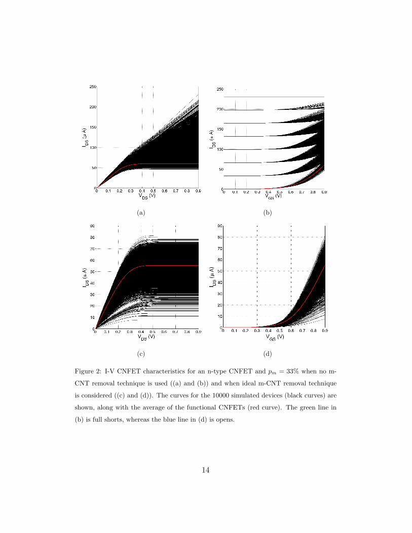
The current characteristics (IDS − VDS and IDS − VGS) for m-CNT elim-
ination scenarios 1) and 3) and for the worst case of m-CNT probability
(pm = 33%) are shown in Fig. 2. The I-V curves for m-CNT removal case
2) are not shown because they are similar to those for 1). The results of this
simulation will be analyzed in the following sections.
Probit plots of ION and IOFF when m-CNTs are not removed and when
an ideal m-CNT removal process is considered are depicted in Fig. 3. These
plots complement the I-V current characteristics showed in the previous Fig-
ure and the data shown in Table 2.
4. Variability analysis
Based on the IDS − VGS current distributions obtained with the CNFET
manufacturing variability methodology presented in Section III.C, and taking
into account only the functional transistors when an ideal m-CNT removal
technique is applied (i.e., ignoring opens), we calculated the mean (µ) and
standard deviation (σ) for several key transistor parameters: ION , ION/IOFF
and VTH (Table 2).
With regard to the behavior of µ and σ vs. pm, it can be seen that in the
case of ION , the mean increases slightly as pm decreases, whereas the STD
decreases. For ION/IOFF , both the mean and the STD decrease slightly as
pm decreases. Finally, VTH remains almost constant for all four pm as in this
study we considered it to be affected only by diameter variations. However,
in terms of variability, the ION and ION/IOFF parameters are highly affected
13
(a) (b)
(c) (d)
Figure 2: I-V CNFET characteristics for an n-type CNFET and pm = 33% when no m-
CNT removal technique is used ((a) and (b)) and when ideal m-CNT removal technique
is considered ((c) and (d)). The curves for the 10000 simulated devices (black curves) are
shown, along with the average of the functional CNFETs (red curve). The green line in
(b) is full shorts, whereas the blue line in (d) is opens.
14

(a) (b)
(c) (d)
Figure 3: Probit plots of ION and IOFF when no m-CNT removal technique is used and
for pm = 33% ((a) and (b)) and when ideal m-CNT removal technique is considered and
for four different pms ((c) and (d)).
by CNT count variations, yielding variability values (3σ/µ) between 46.98%
and 185.67% (pm = 33%) and 24.89% and 96.81% (pm = 1%), respectively.
15

Table 2: Mean and STD when ideal m-CNT removal technique is applied (only functional
transistors)
pm = 33% pm = 10% pm = 5% pm = 1%
µ σ µ σ µ σ µ σ
ION (µA) 55.47 8.78 59.75 5.69 60.06 5.24 60.14 4.99
ION/IOFF (×105) 12.7 7.86 9.25 3.37 8.60 2.81 8.15 2.63
VTH (V) 0.26 0.02 0.26 0.02 0.26 0.01 0.25 0.01
Threshold voltage presented a more moderate fluctuation of about 12%.
It is worth noting that in the case considered (ideal m-CNT removal
method, pmR = 100%), it is possible to achieve a very high ION/IOFF in the
order of 105-106. However, the presence of m-CNTs severely degrades it. As
shown in [31], the ION/IOFF ratio of a CNFET composed of a mixture of
s-CNTs and m-CNTs can be calculated as:
IONIOFF
=NsIs,on +NmImNsIs,off +NmIm
(2)
where Ns and Nm are the number of s-CNTs and m-CNTs, respectively;
Is,on and Is,off are the ON and OFF currents of an s-CNT as defined in
Section III.A above; and Im is the current delivered by an m-CNT when
VDS = 0.9V , and it is the same for both the ON and OFF states.
When the CNFET circuit level is considered (for multiple transistors),
the most adequate parameter is the ratio of the mean values of ION and
IOFF :
16

µ(ION)
µ(IOFF )=
µ(Ns)µ(Is,on) + µ(Nm)µ(Im)
µ(Ns)µ(Is,off ) + µ(Nm)µ(Im)(3)
where
µ(Ns)
µ(Nm)=
ps(1− psR)
pm(1− pmR)(4)
when an m-CNT removal process is applied.
Using these equations and the mean of the ON and OFF currents obtained
through the 10000 MC simulations, Fig. 4 illustrates how the presence of m-
CNTs in the transistors affects the average ION/IOFF ratio for the four pm
probabilities assumed and for different psR. It should be observed that the
average ratio improves as pm and psR decrease and pmR increases as expected.
It should likewise be noted that this ratio remains almost constant once pmR
approaches 100%. Moreover, it is in the range of 105 − 106 (inset in Fig. 4)
and fluctuates slightly as the pm changes, as seen in Table 2.
5. Statistical reliability analysis
The main causes of failure in CNFETs are the presence of m-CNTs in
the transistor and CNT count variations due to density fluctuations and the
application of m-CNT removal processes. An open occurs when there is no
CNT bridging the source and drain contacts; a short is caused by the presence
of one or more m-CNTs in the transistor.
Many previous publications have presented analytical models to evaluate
the impact of CNT density and count variations and of m-CNTs on CNFET
devices and circuits. In [32], a compact model for the probability of failure
in CNFETs is presented that includes m-CNTs and density variations based
17

Figure 4: Average ION/IOFF ratio vs. probability of m-CNT survival. (Inset) Zoom when
1− pmR is between 10−7 and 10−10.
on a binomial probability distribution. In [15], a probabilistic framework
for modeling the CNT count distribution in a CNFET of a given width is
developed and used to estimate the CNT count yield of a CNFET when an
ideal m-CNT removal process is applied. That model thus takes only open
defects into account.
As an extension of these two previous analytical models, a CNFET fail-
ure model is derived and presented in this section. CNFET failure model
proposed in [32] considers both open and short defects that are due to CNT
density variations (“void CNFET”) and the presence of m-CNTs, respec-
18
tively. That is, m-CNTs are not removed (pmR=0 and psR = 0). CNFET
failure model presented in [15] only considers open defects that are due to
CNT density variations and the application of a m-CNT removal process in
which all m-CNTs are eliminated and maybe also some s-CNTs are removed
(pmR=1 and psR = 0 or psR 6= 0). Our model does not consider CNT den-
sity variations (a uniform CNT density is assumed) but it is accurate when
m-CNTs are not removed (pmR=0 and psR = 0) as well as and ideal (pmR=1
and psR = 0) or non-ideal m-CNT removal (pmR=1 or pmR < 1 and psR = 0
or psR 6= 0) process is applied.
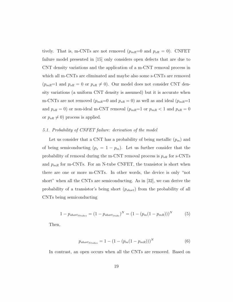
5.1. Probability of CNFET failure: derivation of the model
Let us consider that a CNT has a probability of being metallic (pm) and
of being semiconducting (ps = 1 − pm). Let us further consider that the
probability of removal during the m-CNT removal process is psR for s-CNTs
and pmR for m-CNTs. For an N-tube CNFET, the transistor is short when
there are one or more m-CNTs. In other words, the device is only “not
short” when all the CNTs are semiconducting. As in [32], we can derive the
probability of a transistor’s being short (pshort) from the probability of all
CNTs being semiconducting
1− pshortNtubes= (1− pshort1tube)N = (1− (pm(1− pmR)))N (5)
Then,
pshortNtubes= 1− (1− (pm(1− pmR)))N (6)
In contrast, an open occurs when all the CNTs are removed. Based on
19

[15], the probability of an open for an N-tube CNFET can be calculated as
popenNtubes= (pmpmR + pspsR)N (7)
Therefore, the overall probability of failure of a single N-tube CNFET is
given by
pf = pshortNtubes+ popenNtubes
(8)
It should be noted that the reliability of CNFETs at the circuit level
was studied in [38]. That study derives the probability of failure of a chip
consisting of M transistors (i) when the M CNFETs are independent of each
other (uncorrelated) and (ii) when some of the M CNFETs are correlated,
that is, when they share the CNTs. If CNFETs are perfectly correlated, a
circuit’s probability of failure can be reduced.
Using Eq. 8, Figure 5 shows the probability of CNFET failure versus the
average number of CNTs in the channel for the three m-CNT removal cases
and for different pm.
When m-CNTs are not eliminated, the probability of failure is the prob-
ability of a short. Note that it is quite high for all four m-CNT probabilities
and that it increases as N and pm increase (Fig. 5a) -i.e. the probability of
failure for pm = 33% rises above 0.9 when the average number of CNTs is
more than 7. As noted, m-CNTs are thus the main cause of CNFET failure
and so different options to deal with this “m-CNT problem” and decrease
this high probability of short have been proposed. These include: 1) self-
sorting m-CNT techniques [20], 2) selective etching of m-CNTs [22], [24],
3) electrical burning of m-CNTs [21], and 3) metallic-CNT-tolerant design
methodology (ACCNT) [39]. Shorts are also illustrated in Fig. 2(b). The
20

(a) (b)
(c) (d)
Figure 5: Probability of CNFET failure vs. average CNTs: (a) when no m-CNTs are
removed; (b) when an ideal m-CNT removal process is considered; and (c) and (d) when
a non-ideal m-CNT removal process is applied for pmR = 100% and pmR = 99.99%,
respectively.
21

black curves representing a very high IOFF (∼ 10−6A) are shorts when one or
more CNTs are metallic, while the green lines are shorts when all 7 CNTs are
metallic. We have called these situations partial − short and full − short,
respectively. A percentage of shorts as high as 94% can be obtained for the
worst pm case considered.
In contrast, in the case of an ideal m-CNT removal process, the pf is the
probability of an open. As shown in Fig. 5b, it is much lower than in the
previous case and it exhibits the opposite behavior; it decreases as N becomes
bigger. These opens can also be observed in Fig. 2(d) and they account for
0.07% of the samples.
When a non-ideal m-CNT removal technique is applied, two different
behaviors can be observed. If we consider that all m-CNTs and some s-
CNTs are removed (pmR = 100% and psR = 10% − 40%), pf is once again
the probability of an open, as shown in Fig. 5c. This is similar to Fig. 5b, but
presents higher values. In contrast, if a small portion of the m-CNTs survives
(pmR = 99.99% and psR = 10% − 40%), the probability of CNFET failure
is the sum of popen and pshort and it behaves strangely (Fig. 5d), declining
sharply at the outset, before gradually rising back up. This is because at first
the probability of an open is the dominant component, but, as the average
number of CNTs increases, the probability of a short becomes dominant. It
should moreover be noted that the probabilities of failure are different for a
single pm for the two psR considered when N is small, but that they become
identical as of a given value of N - i.e. for large N the probability of CNFET
failure is dominated by the probability of short and it is independent of psR.
Finally, it is worth noting that there is an optimum average number of CNTs
22

to minimize the probability of failure in this last case.
6. Conclusion
This paper presents a complete reliability and variability study of carbon
nanotube technology in the presence of CNFET manufacturing imperfec-
tions, giving a realistic view of the challenges these devices face today and
evaluating the impact of these manufacturing issues on CNFET performance.
First, we introduced a methodology to analyze the main sources of vari-
ability in the CNFET manufacturing process, such as CNT diameter, doping
and density fluctuations, and the presence of metallic CNTs. This method,
which is based on a MATLAB script and the Stanford CNFET HSPICE
model, is able to simulate heterogeneous (non-ideal) transistors, that is, CN-
FETs with different numbers of tubes that have different diameters, are not
uniformly spaced, have different source/drain doping levels, and, most im-
portantly, are made up not only of semiconducting CNTs but also metallic
ones, this latter factor being one of the biggest challenges in CNFET tech-
nology today. We performed 10000 Monte Carlo simulations for an n-type
CNFET (N=7), considering different m-CNT removal scenarios and m-CNT
probabilities (pm): (i) when no removal technique is used; (ii) when an ideal
removal method is considered; and (iii) when a non-ideal m-CNT removal
process is applied.
Furthermore, a model for analyzing CNFET failures was derived. The
model takes into account both opens and shorts and is accurate for different
m-CNT removal scenarios.
From the point of view of reliability, the presence of m-CNTs and varia-
23

tions in the CNT count are the main causes of failure. Metallic CNTs must
be eliminated because they result in shorts. In 1-tube CNFETs, there is a
1% probability of a short with just a 1% probability of m-CNTs; this prob-
ability grows higher in multi-channel CNFETs. Different m-CNT removal
techniques are used to reduce the probability of a CNFET short, but their
use increases the variations in CNT count; in other words, by reducing the
average number of CNTs in the transistor, they increase the probability of
an open. If a non-ideal m-CNT removal process is used, some s-CNTs are
eliminated and a small percentage of m-CNTs survives; there is a unique
optimum average number of CNTs. It should be noted that for the best
case considered (pm = 1%, pmR = 99.99%, and psR = 10%), the minimum
probability of CNFET failure was in the order of 10−4, which is very high for
VLSI systems. If an ideal m-CNT removal process could be used, between 5
and 20 CNTs would be required to ensure a pf = 10−10 and, thus, a yield of
∼ 100%.
From the point of view of variability, when an ideal m-CNT removal
process was considered, ION and ION/IOFF parameters were highly affected
by count variations, yielding variability values (3σ/µ) of 47.49% and 185.67%,
respectively, for the worst-case (pm = 33%) scenario. Threshold voltage
showed a more moderate fluctuation of about 12% and remained almost
constant for all pm cases. It should be pointed out that CNFETs in which all
m-CNTs are removed have a high ION/IOFF ratio of ∼ 106, but the presence
of m-CNTs in the transistor severely degrades it.
Today, great efforts are being made to improve CNFET device processing
and to optimize CNFET circuit design techniques. Only in this way can
24

CNT technology become one of the most viable options for minimum-size
transistors of less than 7nm, which are expected to be produced by the early
2020s.
Acknowledgments
This research was partially funded by the Spanish Ministry of Economy
and Competitiveness (MINECO) under the project TEC2008-01856, with
additional funding from the ERDF and the EU TRAMS (248789) project.
The research group is considered a consolidated group by the MINECO and
the Catalan government.
References
[1] G. Roy, A. Brown, F. Adamu-Lema, S. Roy, and A. Asenov, “Simula-
tion Study of Individual and Combined Sources of Intrinsic Parameter
Fluctuations in Conventional Nano-MOSFETs,” IEEE Trans. Electron
Devices, vol. 53, no. 12, pp. 3063–3070, Dec. 2006.
[2] (2011) The ITRS website. [Online]. Available: http://www.itrs.net/
[3] T. Durkop, S.A. Getty, E. Cobas, and M.S.. Fuhrer, “Extraordinary
mobility in semiconducting carbon nanotubes,” Nano Lett., vol. 4, no. 1,
pp. 35–39, 2004.
[4] A. Javey, J. Guo, Q. Wang, M. Lundstrom, and H. Dai, “Ballistic carbon
nanotube field-effect transistors,” Nature, vol. 424, no. 6949, pp. 654–
657, 2003.
25

[5] A.D. Franklin, M. Luisier, S.-J. Han, G. Tulevski, C.M. Breslin,
L. Gignac, M.S. Lundstrom, and W. Haensch,“Sub-10 nm Carbon Nan-
otube Transistor,” Nano Lett., vol. 12, no. 2, pp. 758–762, Jan. 2012.
[6] L. Ding, S. Liang, T. Pei, Z. Zhang, S. Wang, W. Zhou, J. Liu, and
L.M Peng, “Carbon nanotube based ultra-low voltage integrated cir-
cuits: Scaling down to 0.4V,” App. Phys. Lett., vol. 100, no. 26, pp.
263116–263116-5, Jun. 2012.
[7] N. Patil, J. Deng, S. Mitra, and H.-S.P. Wong, “Circuit-Level Per-
formance Benchmarking and Scalability Analysis of Carbon Nanotube
Transistor Circuits,” IEEE Trans. Nanotechnol., vol. 8, no. 1, pp. 37–45,
2009.
[8] C.G. Almudever, and A. Rubio, “Carbon nanotube growth process-
related variability in CNFETs,” in Proc. IEEE Conf. Nanotechnol.,
2011, pp. 1084–1087.
[9] A. Raychowdhury, V.K. De, J. Kurtin, S.Y. Borkar, K. Roy, and A. Ke-
shavarzi, “Variation Tolerance in a Multichannel Carbon-Nanotube
Transistor for High-Speed Digital Circuits,” IEEE Trans. Electron De-
vices, vol. 56, no. 3, pp. 383–392, 2009.
[10] G.M. Landauer, and J.L. Gonzalez, “Radio-Frequency Performance of
Carbon Nanotube-Based Devices and Circuits Considering Noise and
Process Variation,” IEEE Trans. on Nanotech., vol. 13, no. 2, pp. 228–
237, 2014.
26

[11] C.G. Almudever, and A. Rubio, “Variability and Reliability Analysis of
CNFET in the Presence of Carbon Nanotube Density Fluctuations,” in
Conf. Mixed Des. Integr. Circuits Syst., 2012, pp. 124–129.
[12] J. Zhang, N. Patil, H.-S.P. Wong, and S. Mitra, “Overcoming carbon
nanotube variations through co-optimized technology and circuit de-
sign,” in Proc. Int. Electron Dev. Meeting, Dec. 2011, pp. 4.6.1–4.6.4.
[13] N. Patil, A. Lin, E.R. Myers, K. Ryu, A. Badmaev, C. Zhou, H.-
S.P. Wong, and S. Mitra,“Wafer-scale growth and transfer of aligned
single-walled carbon nanotubes,” IEEE Trans. Nanotechnol.,vol. 8,
no. 4, pp. 498–504, Jul. 2009.
[14] N. Patil, A. Lin, E.R. Myers, H.-S.P. Wong, and S. Mitra, “Inte-
grated Wafer-scale Growth and Transfer of Directional Carbon Nan-
otubes and Misaligned- Carbon-Nanotube-Immune Logic Structures,”
in Proc. Symp. VLSI Tech., 2008, pp. 205–206.
[15] J. Zhang, N.P. Patil, A. Hazeghi, H.-S.P. Wong and S. Mitra, “Char-
acterization and Design of Logic Circuits in the Presence of Carbon
Nanotube Density Variations,” IEEE Trans. on Comput-Aided Des.
Integr. Circuits Syst.,vol. 30, no. 8, pp. 1103–1113, 2011.
[16] S.W. Wong, T. Banks, and J.-A. Rogers, “Improved density in aligned
arrays of single-walled carbon nanotubes by sequential chemical vapor
deposition on quartz,” Advanced Mat.,vol. 22, no. 45, pp. 1826–1830,
2010.
27

[17] M.M. Shulaker, H. Wei, N. Patil, J. Provine, H.-Y. Chen, H.-S.P. Wong,
and S. Mitra, “Linear Increases in Carbon Nanotube Density Through
Multiple Transfer Technique,” Nano Lett.,vol. 11, no. 5, pp. 1881–1886,
2011.
[18] L. Qu, D. Feng, and L. Dai, “Preferential Syntheses of Semiconducting
Vertically Aligned Single-Walled Carbon Nanotubes for Direct Use in
FETs,” Nano Lett., vol. 8, no. 9, pp. 2682–2687, 2008.
[19] T. Mizutani, H. Ohnaka, Y. Okigawa, S. Kishimoto, and Y. Ohno, “A
study of preferential growth of carbon nanotubes with semiconducting
behavior grown by plasma-enhanced chemical vapor deposition,” Jour-
nal of Applied Phys., vol. 106, no. 7, pp. 073705–073705-5, Oct. 2009.
[20] M. LeMieux et. al, “Self-sorted, aligned nanotube networks for thin-film
transistors,” Science, vol. 321, no. 5885, pp. 101–104, 2008.
[21] P. Collins, S. Arnold, and P. Avouris, “Engineering carbon nanotubes
and nanotube circuits using electrical breakdown,” Science, vol. 292, pp.
706–709, 2001.
[22] G. Zhang, P. Qi, X. Wang, Y. Lu, X. Li, R. Tu, S. Bangsaruntip,
D. Mann, L. Zhang, and H. Dai,“Selective etching of metallic carbon
nanotubes by gas-phase reaction,” Science, vol. 314, no. 5801, pp. 974–
977, Nov. 2006.
[23] H. Wei, N. Patil, J. Zhang, A. Lin, H.-Y. Chen, H.S. Wong, and S. Mi-
tra, “Efficient Metallic Carbon Nanotube Removal Readily Scalable to
28
Wafer-Level VLSI CNFET Circuits,” in Proc. Symp. VLSI Tech., Jun.
2010, pp. 273–238.
[24] .H. Jin et al., “Using nanoscale thermocapillary flows to create arrays
of purely semiconducting single-walled carbon nanotubes,” Nature Nan-
otech., vol. 8, pp. 347–355, Apr. 2013.
[25] Q. Cao, S.-J. Han, G.S. Tulevski, A.D. Franklin, and W. Haen-
sch,“Evaluation of Field-Effect Mobility and Contact Resistance of Tran-
sistors That Use Solution-Processed Single-Walled Carbon Nanotubes,”
ACS Nano, vol. 6, no. 7, pp. 6471–6477, Jun. 2012.
[26] Q. Cao, S.-J. Han, G.S. Tulevski, Y Zu, D.D. Lu, and W. Haen-
sch,“Arrays of single-walled carbon nanotubes with full surface coverage
for high-performance electronics,” Nature Nanotech., vol. 8, pp. 180–186,
Jan. 2013.
[27] D. Shahrjerdi, A.D. Franklin, S. Oida, J.A. Ott, G.S. Tulevski, and
W. Haensch,“High-Performance Air-Stable n-Type Carbon Nanotube
Transistors with Erbium Contacts,” ACS Nano, vol. 7, no. 9, pp. 8303–
8308, Sept. 2013.
[28] H. Wei, H.-Y. Chen, L. Liyanage, H.S. Wong, and S. Mitra, “Air-Stable
Technique for Fabricating n-Type Carbon Nanotube FETs,” in Proc.
Int. Electron Dev. Meeting, Dec. 2011, pp. 23.2.1–23.2.4.
[29] Y. Chai, A. Hazeghi, T. Kuniharu, H.-Y. Chen, P.C.H. Chan, A. Javey,
and H.-S.P. Wong, “Low-Resistance Electrical Contact to Carbon Nan-
29

otubes With Graphitic Interfacial Layer,” IEEE Trans. on Elect. De-
vices, vol. 59, pp. 12–19, 2012.
[30] Z. Chen, J. Appenzeller, J. Knoch, Y.-Ming. Lin and P. Avouris, “The
role of metal-nanotube contact in the performance of carbon nanotube
field-effect transistors,” Nano Lett., vol. 5, no. 7, pp. 1497–1502, Jun.
2005.
[31] J. Zhang, N. Patil, and S. Mitra, “Probabilistic analysis and design of
metallic-carbon-nanotube-tolerant digital logic circuits,” IEEE Trans.
Comput.-Aided Des. Inter. Circuits Syst., vol. 28, no. 9, pp. 1307–1320,
2009.
[32] P. Zarkesh-Ha, and A.A. Shahi,“Stochastic analysis and design guide-
lines for CNFETs in gigascale integrated systems,” IEEE Trans. Elec-
tron Devices, vol. 58, no. 2, pp. 530–539, 2011.
[33] B. Ghavami, M. Raji, H. Pedram, and M. Pedram,“Statistical Func-
tional Yield Estimation and Enhancement of CNFET-Based VLSI Cir-
cuits,” IEEE Trans. on VLSI Systems, no. 99, pp. 1–14, 2012.
[34] J. Deng, and H.-S. Wong, “A Compact SPICE Model for Carbon-
Nanotube Field-Effect Transistors Including Nonidealities and Its Ap-
plicationPart I: Model of the Intrinsic Channel Region,” IEEE Trans.
Electron Devices, vol. 54, no. 12, pp. 3186–3194, 2007.
[35] J. Deng, and H.-S. Wong, “A compact spice model for carbon-nanotube
field-effect transistors including nonidealities and its application part II:
30

Full device model and circuit performance benchmarking,” IEEE Trans.
Electron Devices, vol. 54, no. 12, pp. 3195 –3205, 2007.
[36] (2008) The Stanford University CNFET model website. [Online]. Avail-
able: http://nano.stanford.edu/model.php?id=23
[37] J. Deng, and H.-S. Wong, “Modeling and analysis of planar gate ca-
pacitance for 1-D FET with multiple cylindrical conducting channels,”
IEEE Trans. Electron Devices, vol. 54, no. 9, pp. 2377–2385, 2007.
[38] J. Zhang, S. Bobba, N. Patil, A. Lin, H.-S. Wong, G. De Micheli,
and S. Mitra “Carbon Nanotube Correlation: Promising Opportunity
for CNFET Circuit Yield Enhancement,” in Proc. Design Automation
Conf., Jun. 2010, pp. 889–892.
[39] A. Lin, N. Patil, ,H. Wei, S. Mitra, and H.-S. Wong, “ACCNT:
A Metallic- CNT-Tolerant Design Methodology for Carbon Nanotube
VLSI: Analyses and Design Guidelines,” IEEE Trans. Electron Devices,
vol. 57, no. 9, pp. 2284–2295, 2010.
31