understand' elf - americanradiohistory.coms law-voltage-dropper circuit-power in the...
TRANSCRIPT

UNDERSTAND'
ELF

No. 1553$15.95
UNDERSTANDING
ELECTRONICS2ND EDITION
BY R. H. WARRING
TAB TAB BOOKS Inc.BLUE RIDGE SUMMIT, PA 17214

Other TAB Books by the Author
No. 1142 84 Practical IC Projects You Can BuildNo. 1493 Electronic Components Handbook for Circuit DesignersNo. 1593 Understanding Digital ElectronicsNo. 1673 Robots and RobotologyNo. 1853 Logic Made Easy
SECOND EDITION
THIRD PRINTING
Copyright © 1984 by TAB BOOKS Inc.
Printed in the United States of America
Reproduction or publication of the content in any manner, without expresspermission of the publisher, is prohibited. No liability is assumed with respectto the use of the information herein.
Understanding Electronics was originally published in 1978.Printed by permission of Lutterworth Press.
Copyright © 1984, 1978 by R. H. Warring
Library of Congress Cataloging in Pubiication Data
Warring, R. H. (Ronald Horace), 1920-1984Understanding electronics.
Includes index.1. Electronics-Amateurs' manuals. I. Title.
TK9965.W39 1984 621.38 83-24112ISBN 0-8306-0253-4ISBN 0-8306-0153-8 (pbk.)
Contents
Preface to Second Edition
Introduction
vi
vii
List of Working Circuits to Build and/or Experiment With ix
1 Units, Abbreviations, and Symbols
2 Dc and Ac
3 Basic Circuits and Circuit LawsOhm's Law-Voltage-Dropper Circuit-Power in the Circuit-Shunt Circuits-Ammeter into Voltmeter-Dividers-Basic AcCircuits-Power Factor
4 ResistorsColor Code-Power Rating-Voltage Rating-Wire-woundResistors-Variable Resistors-Circuit Rules for Resistors
5 CapacitorsFixed Capacitors-Nonpolarized Capacitor Types-ElectrolyticCapacitors-Variable Capacitors-Basic Circuit Rules forCapacitors
6 Capacitor and RC CircuitsTime Constant-Capacitors in Ac Circuits-Simple Coupling-Filter Circuits-Low-pass Filters-High-pass Filters
1
5
10
21
30
37

7 Coils and Inductances 46Resonant Circuits-Tuned Circuits-Series-resonant Circuits-Radio Frequency Chokes
8 Transformers 54Transformers as Power Supplies-Transformers as CouplingDevices-Autotransformers
9 SemiconductorsTransistors-Practical Diodes-Basic Transistor Circuits-Transistor Construction-Field-effect Transistors
59
10 Neon Lamps, LEDs and Liquid Crystals 71LEDs-Liquid Crystal
11 Other Components 78The Diode Family-The Phototransistor-Solar Cells-Rec-tifiers-Thermistors and Sensistors
12 TubesDiodes-Triodes and Tetrodes-Pentodes-The Cathode-rayTube
13 Integrated CircuitsMonolithic and Hybrid ICs-MSI and LSI-Op Amps-DigitalSystems Cs-Analog and Digital Computers
21 Printed CircuitsPlanning the Circuit Drawing-Final Drawing-Etching-Mounting and Soldering-Simplified Printed Circuit Construction .
22 RadioDetection-FM Detector-Amplifier Stages-Output Stage-The Superhet
23 Television
24 Microprocessors
25 BatteriesDry Batteries (Primary Batteries)-Alkaline-manganese Cells-Mercury Cells-Silver-oxide Cells-Secondary Batteries-General Battery Rules
143
149
159
164
168
26 Power Supplies and Chargers 181
88 Battery Chargers-Dc Input Chargers
27 High -voltage Power Supplies 185Filters-Output Voltage-Voltage Stabilization-Bias Volt -
93 ages-Voltage Dividers-Voltage Multipliers-Variable-voltageSupplies-Stabilized Tube Heater Supplies-Transistor PowerSupplies
14 IC Arrays 101
15 Transistor Characteristics 105DC Parameters-Input Characteristics-Transfer Charac-teristics-Output Characteristics-Current Amplification -DcCurrent Gain-Manufacturer's Specifications
16 Basic Guide to Selecting TransistorsPro -Electron Coding-Identifying Transistors by Shape
17 AmplifiersBasic Amplifier Circuits
18 OscillatorsResonant -frequency Oscillators-Practical LC Oscillators-Crystal-controlled Oscillators-Phase-shift Oscillators-BridgeOscillators
112
115
124
19 Circuit Diagrams 131
20 Circuit Construction 137Pinboard Construction-Skeleton Assembly-Bonded Mount-ing-Bus-bar Assembly-Tagboard Assembly-Pegboard Con-struction
Index 196

Preface to Second Edition
Understanding Electronics was originally written as a basic guide for homebuilders of electronic circuits with a particular emphasis on components,how they work, and how they go together to make complete circuits. Theaim was to make circuit diagrams more understandable and also set downthe "facts and figures" to undertake original circuit design, or to designsimple basic circuits from scratch.
Judging by reader response, it has succeeded in this and has also raisedmany further queries and problems. The second edition has been expandedto cover these and other subjects, to increase both the scope and usefulnessof the book. At the same time the opportunity has been taken to revise andupdate as necessary all the original material retained.
In particular, the not -so -expert electronic hobbyist should find the newChapters 15 and 16-Transistor Characteristics and a Basic Guide toSelecting Transistors-especially helpful and worth studying in some de-tail. There are also new chapters on amplifiers and oscillators, againexpanding the coverage of the original book, and more information onpower supplies, particularly those designed for high -voltage applications.And, for good measure, a chapter introducing the subject of microproces-sors has been included together with a considerable number of new illus-trations and circuit diagrams.
vi
Introduction
If you find electronics difficult to understand-then you are among the vastmajority! One good reason for this is that you cannot "see" how electroniccircuits work-only switch them on and hope that they do work. So homeconstruction of electronic circuits may seem something of a gamble, nothelped by the fact that the "plans" are usually in the form of theoreticalcircuit diagrams with components designated by symbols instead of theirphysical shape and size, and quite probably in nothing like the arrangementthey will appear on a practical working circuit.
Take heart at this point! In at least nine cases out of ten, if a circuit builtto a published plan does not work, it will be for one of two simple reasons:either poorly made connections or wrong connections. The only mysteryabout that is that it happens-even to experts.
The study of electronic circuits is a study of electronic components andhow they behave when connected together in various ways. This book setsout to explain just that, in simple easy -to -understand fashion, without anydifficult mathematical calculations or theoretical explanations -what theyare, what they look like, what they do, and what sort of circuits they areused in. A basic groundwork in the practical side of simple electronics-andthe subject can be quite simple. And to make the subject more realistic,there are fifty-one suggested working circuits to build, or experiment with.
There is still the question of how to read and understand circuitdrawings, and turn them into practical working circuits, so separate chap-ters are devoted to these two particular subjects. There is also a chapter onprinted -circuit construction.
Since most simple electronic circuits are battery powered, the subjectof different battery types and their performances is also covered in some
vii
detail. Also included are circuits for building a battery charger, either tooperate off the mains or from a car battery.
Understanding Electronics should be an excellent starter for anyonewanting to take up practical electronics as a hobby interest-and an idealreference to back up, and make it easier to understand, the types andconstruction of more elaborate circuits described in rather more advancedbooks, monthly journals, and so on. It should prove invaluable as a source ofinformation which has been left out of other electronic books on the author'sassumption that "everyone should know that." In fact, such books are oftendescribed as "too technical" or "too advanced." So this present book shouldfill that particular gap.
viii
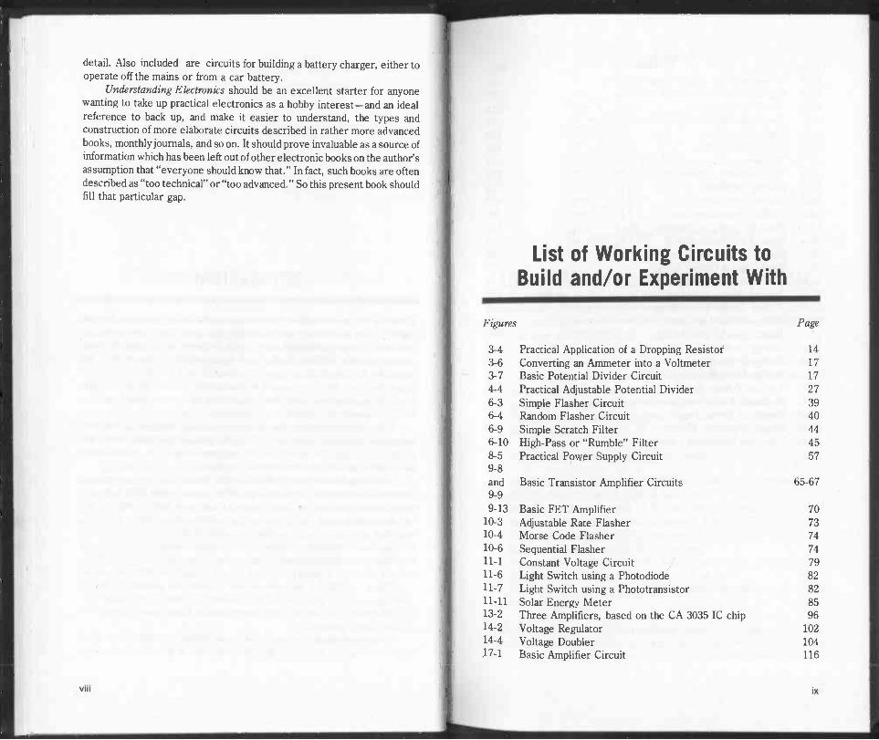
List of Working Circuits toBuild and/or Experiment With
Figures Page
3-4 Practical Application of a Dropping Resistor 14
3-6 Converting an Ammeter into a Voltmeter 173-7 Basic Potential Divider Circuit 174-4 Practical Adjustable Potential Divider 276-3 Simple Flasher Circuit 396-4 Random Flasher Circuit 406-9 Simple Scratch Filter 446-10 High -Pass or "Rumble" Filter 458-5 Practical Power Supply Circuit 579-8and Basic Transistor Amplifier Circuits 65-679-99-13 Basic FET Amplifier 70
10-3 Adjustable Rate Flasher 7310-4 Morse Code Flasher 7410-6 Sequential Flasher 7411-1 Constant Voltage Circuit 7911-6 Light Switch using a Photodiode 8211-7 Light Switch using a Phototransistor 8211-11 Solar Energy Meter 8513-2 Three Amplifiers, based on the CA 3035 IC chip 9614-2 Voltage Regulator 10214-4 Voltage Doubler 10417-1 Basic Amplifier Circuit 116
ix

Figures Page17-2 Crystal set with Single -Stage Amplifier 116
17-3 Crystal set with Two -Stage Amplifier 117
17-6 Two -Stage Amplifier 119
17-7 Two -Stage Amplifier with Volume Control 120
17-8 Class -A Amplifier 120
17-9 Push -Pull Amplifier 121
17-10 Transformer -Coupled Push -Pull Amplifier 122
18-3 Self -Oscillating Oscillator 126
18-5 Hartley Oscillator 127
18-6 Colpitts Oscillator 127
18-8 1 -MHz Crystal Oscillator 128
18-11 Basic LC Oscillator Circuit 130
22-4 Basic AM detector Circuit 153
22-5 Basic FM detector Circuit 153
22-7 Basic Class A Output Circuit 155
22-8 Basic Class B Output Circuit 156
26-1 Battery charger with stabilized output (mains operated) 182
26-4 Battery charger for working off a 12 -volt battery 184
27-6 Voltage Stabilizing Circuit with Zener Diodes 190
27-7 Stabilization by Bias Voltage 190
27-8 Voltage Divider 191
27-9 Voltage Multiplier 191
27-10 Voltage Multiplier using Diodes 192
27-11 Variable -Voltage Supply 192
27-12 Stabilized Heater Supply 193
27-13 Transistor Power Supply 193
27-14 Simple Regulation Circuit 194
27-15 Low -Loss Stabilizing Circuit 194
x
Chapter 1
Units, Abbreviations, and SymbolsIn electronics there are seven basic units to measure quantities which
define what is going on in a circuit. These are (together with the lettersymbols used as abbreviations):
Volts (V)-a measure of the potential, cmf (electromotive force), orvoltage in a circuit. For practical purposes, potential difference, emfand voltage all really mean the same thing.Amps (A)-a measure of the current flowing in a circuit.Watts (W)-a measure of the power developed by the flow of currentthrough a circuit.
The other four refer to the effect of components in the circuit, viz:
Ohms (fl)-a measure of the resistance or individual resistances in acircuit when the current flow is direct (dc).Impedance (Z)-a measure of the effective resistance or individual
resistances in a circuit when the current flow is alternating (ac).Farads (F) -a measure of the capacitor present in a circuit or producedby individual components, i.e., capacitors.Henrys (H)-a measure of the inductance present in a circuit orproduced by individual components such as coils.Reactance (X)-the combined effect of inductance and capacitance inan ac circuit.
Capital letters are also used as abbreviations for voltage and current.Strictly speaking E (foremf) is the correct symbol for a voltage source, withV (for volts) in other parts of the circuit. Vs can be used instead of E for a
1

source voltage. The capital letter I is used for current. In some circuitslowercase letters are used to indicate voltages and currents flowing indifferent parts of a circuit, e.g., v and i, respectively. These may have areference annotation attached, particularly in the case of transistor circuits,e.g., ve, describing emitter voltage.
The relationship between units is explained in Chapter 3. There arealso various other units employed in electronics, the use and meaning ofwhich will be made clear in appropriate chapters.
In practical circuits, numerical values of these units may be very large,or very small. Resistance values, for example, may run to millions of ohms.Capacitor values may be in millionths or even million -millionths of a farad.To avoid writing out such values in full, prefixes are used to designate thenumber associated with the particular value involved. Again the symbolrather than the full prefix is normally used:
mega (M)-meaning times 1,000,000kilo (k)-meaning times 1,000milli (m)-meaning divided by 1,000 (or 1/1,000th)mkro(µ)-meaning divided by 1,000,000 (or 1/1, 000,000th)nano (n)-meaning divided by 1,000,000,000 (or 1/1, 000,000,000th)pica (p)-meaning divided by 1,000,000,000,000 (or
1/1, 000, 000, 000, 000)
For example, instead of writing out 22,000,000 ohms in full, this would beshown as 22 Mohms, or, more usually 22 Mfl, using symbols both for theprefix and basic unit. Similarly a capacitor value of 0.000,000,000,220farads would be shown as 220 picaF, or, more usually 220 pF.
The multipliers (M and k) are most commonly associated with values ofresistors, and also for specifying radio frequencies. The lowest divisor (m) ismost usually associated with the values of current typical of transistorcircuits, etc. It is also used to specify most practical values of inductances.The larger divisors (12, n and p) are most commonly associated withcapacitor values.
Single capital letter abbreviations are also used for components. Themain ones are:
C -for capacitorsD -for diodes (also sometimes CR)L -for coilsR -for resistors
These are all standard and universally accepted abbreviations. With othercomponents this is not always the case. Thus transistors may be designedT, TR, Tr, VT or even Q on circuits originating from different sources. Theuse of TR, Tr, or Q is preferred, leaving the letter T as the abbreviation fortransformers. Note the abbreviation FET (or fet) is used for a field-effecttransistor in text although it may be "Q" in diagrams.
2
In practical circuits, more than one of the same type of components arenormally used. Individual components of the same type are then designated
by numbers (usually reading from left to right across the circuit) associated
with the component symbol (Fig. 1-1) (see also Chapter 3). Thus resistorswould be designated R1, R2, R3; capacitors Cl, C2, C3, . . . and so on.
There is no correct or specific sequence in which such numbers areallocated. They are there only to identify a particular component.
or --i-VSAAr---fixed value resistor
-II- -A-- -0i-capacitor electrolytic
capacitor
-10 OS /- -14-coil diode
- or -Vy4--variable resistor (potentiometer)
variable trimmer
capacitor capacitor
loudspeaker earth battery
Fig. 1-1. Symbols for basic circuit components. Other symbols are given in later
chapters.
Here are some other general abbreviations which are widely used,although again they may be shown in various different ways-capital let-
ters, or lowercase letters in upright or italic, with or without periods. Thusthe abbreviation of alternating current may appear in five different ways:
AC a.c. a.c. ac ac
The general preference is that all such abbreviations should be in lower-case without periods, and so the following abbreviations are shown that
way:
ac -alternating currentof-audio frequencyagc -automatic gain controlam*-amplitude modulated (or amplitude modulation)dc-direct currenteht -extra high tensionfm*-frequency modulated (or frequency modulation)hf -high frequencyht -high tensionic -integrated circuitsif-intermediate frequency (also i-f)if-low frequency
3

rf- radio frequencyuhf -ultra high frequencyvhf-very high frequency
*There is a good reason for retaining capital letters for these abbreviationsas AM and FM radios are widely quoted in this way.
4
Chapter 2
Dc and Ac
A basic direct current (dc) circuit is simple enough to understand. A source
of electrical force (such as a battery) is connected via wires to variouscomponents with a return path to the source. Current then circulatesthrough the circuit in a particular direction. Figure 2-1 shows a veryelementary circuit of this type where a battery is connected to a dc electricmotor and is compared with a similar closed loop hydraulic motor in a
simple recirculating system.It is obvious what happens in the hydraulic circuit. The pump is a
source of pressurized water which impinges on the vanes of the hydraulicmotor to drive it. There is a flow of water around the system. At the sametime there will be some loss of pressure energy due to friction of the waterflowing through the pipes and the motor. This is the resistance in thecircuit. But most of the pressure energy delivered by the pump is convertedinto power by the hydraulic motor.
In the electrical circuit counterpart, the battery is a source of electricalpressure (which in simple terms we designate voltage). This forces anelectrical current to flow through the circuit, opposed by the resistanceoffered by the wiring and the electric motor coils. Again, most of theoriginal electrical energy in the battery is converted into power by theelectric motor. Provided the battery voltage does not change, a constantvalue of an -rent will flow through the circuit always in the same direction,and the electric motor will continue to run at a constant speed.
Conventionally, dc current flow is regarded as being from "positive" to"negative" of a battery or any other dc source (such as a dynamo). It is astream flow, just like the water flow in the hydraulic circuit, but the streamIs actually composed of sub -atomic particles or electrons. Unfortunately,after convention had established the "positive to negative" flow definition,
5

electrical pressureelectricmotor
battery resistance
electrical circuit
resistance
hydraulic circuit
Fig. 2-1. An electrical circuit is similar to a hydraulic circuit.
it was found that this electron stream flow was actually from negative toPositive. This does not matter for most practical purposes, but for anunderstanding of how transistors and other solid-state devices work it isnecessary to appreciate this "reverse" working.
"Positive" always seems stronger than "negative," so it is difficult tothink of current as flowing other than from positive to negative. We canrelate this to electrons flowing from negative to positive by thinking ofelectrons as particles of negative electricity. Being "weaker" (negative),they represent a "reverse flow," setting up conditions for a positive flow ofcurrent-from positive to negative. Otherwise, simply forget the differenceand work on the practical fact that + and - are only terms of convenienceused to ensure that components in a circuit which have positive andnegative sides are connected up correctly. This applies mainly to batteries,transistors, diodes, and electrolytic capacitors.
All materials are composed of atoms in which there is a stable balanceof positive and negative charges (except in the atoms of radioactive ele-ments). The application of an electrical pressure will cause electrons to bedisplaced from the atom, leaving it with an effective positive charge. It isthen in a state to attract any stray electrons. Since there is electricalpressure present, this means that there will be a movement of electronsalong the chain of atoms comprising the wiring and component(s) in thecomplete return circuit. It is this movement that constitutes the electriccurrent flowing through the circuit, the strength of the current beingdependent on the number of electrons passing any particular point in thecircuit in a given time. Break the circuit and the pressure is broken, socurrent flow ceases. So, in fact, the analogy with a hydraulic circuit is notreally valid in this instance (the hydraulic pump will still deliver waterunder pressure if its circuit is broken until it has emptied the fluid in thecircuit between the break and the pump).
Atoms of materials like metals will give up electrons readily whensubject to electrical pressure, and so make good conductors of electricity.Atoms of most non-metals, including plastics, are reluctant to give upelectrons even under high electrical pressure, and so are essentially non -
6
conductors. If extremely resistant to giving up atoms, they are classified as
insulators.Summarizing, then, a dc circuit when connected or switched on pro-
vides a constant flow of current in one direction through the circuit as in Fig.
2-2, unless something changes in the circuit (e.g., source voltage changes,
or a circuit resistance value alters). The value of this current is determined
by the source voltage and the total resistance in the circuit (see Chapter 3).
Current flow is also regarded as positive (or positive current).
constant flow
switchon
time switchoff
Fig. 2-2. Direct current flow with constant circuit resistance.
In the case of an ac circuit, the source of electrical pressure continuallyreverses in a periodic manner. This means that current flows through thecircuit first in one direction (positive) and then the other (negative). In
other words, a simple graph of current flow with time will look like Fig. 2-3.The swing from maximum positive to maximum negative is known as theamplitude of the ac current. Also one complete period from zero tomaximum positive, back to zero, down to maximum negative and back tozero again is known as a cycle. These cycles may occur at varying rates from
a few times a second to millions of times a second and define the frequency of
81
switchon
11 4- one cycletime
Fig. 2-3. Alternating current flow is in "cycles" of positive and negative current.
7

the ac current, frequency being equal to the number of cycles per second. Inthe case of the domestic mains supply (in Britain), for example, the fre-quency is 50 cycles -per -second, or 60 cycles -per -second in the U.S. But"cycles -per -second" is an obsolete term. It is now called hertz (abbreviatedHz). Thus standard mains frequency is 50 or 60 Hz.
Apart from the fact that ac is continually swinging from positive tonegative current flow, the other difference compared with dc is that theactual current value present is also changing all the time. It does, however,have an "average" value which can be defined in various ways. The usualone is the Root Mean Square (or rms), which is equal to 0.7071 times themaximum cycle values for sine wave ac such as normally generated by analternator, Fig. 2-4. Alternating current may, however, be generated withother types of waveform.
Fig. 2-4. Peak and Root Mean Square (rms) values of amplitude defined andcompared.
Another characteristic of ac is that both the voltage and current arecontinually changing in similar cycles. Only rarely, however, will thevoltage and current both attain maximum and zero values at exactly thesame time. In other words the current (waveform) curve is displacedrelative to the voltage (waveform) curve, Fig. 2-5. This displacement isknown as a phase difference. It is normally expressed in terms of the ratio ofthe actual displacement to a full cycle length on the zero line, multiplied by360 (since a full cycle represents 360 degrees of ac working). This is calledthe phase angle. Usually the current will "peak" after the voltage (i.e., bedisplaced to the right of the diagram), whereupon the current is said to belagging and the phase angle is referred to as angle of lag.
The use of the term "angle" can be a bit confusing at first. It is really amatter of mathematical convenience, useful in more complicated calcula-tions involving vector diagrams. For a general understanding of ac it isbetter to think of angle as meaning a particular "number point" on a linelength representing one full cycle divided into 360 divisions. Thus a phaseangle of 30 degrees can be understood as a point 30/360ths along that line.
8
voltage currente"'\
current legging by 1 cycle or 90 degrees
one complete cycle - 360 degrees
Fig. 2-5. Current usually "lags" behind voltage in an alternating current circuit.
Phase difference (phase angle) can be an important factor in the designand working of many alternating current circuits because when a current
"lags" (or "leads") the voltage, the timing aspects of a circuit are affected.

Chapter 3
Basic Circuits and Circuit LawsAs noted in Chapter 2, the current which flows in a simple dc circuit isdependent on the applied voltage and the resistance in the circuit. Voltagecan be measured directly by a voltmeter placed across the battery (or dcsource) terminals; and current by an ammeter connected in series in thecircuit, as in Fig. 3-1. This diagram also shows the circuit components insymbolic form (in the case of a resistor this can be drawn as a plain rectangleor a zig-zag line).
OHM'S LAW
The relationship between voltage (E), current (I) and resistance (R) isgiven by Ohm's law:
In plain language:
amps -
I = -R
voltsresistance in ohms
or the formula can be rewritten:
volts = amps x ohms
voltsohms =
amps
10
ammeter
resistor
battery
voltmeter
alternative symbols
Fig. 3-1. Basic dc circuit drawn in two ways, with meters for measuring current
and voltage indicated.
This is one of the most basic and most useful laws of electronics and isequally applicable to ac circuits which are purely resistive (i.e., do not haveadditional "resistance" effects produced by the current being alternatingrather than steady).
Ohm's law makes it possible to calculate (and thus design) the perfor-mance of a simple dc circuit. For example, suppose we need a current of 200milliamps (mA) to flow in a particular circuit to be powered by a 6 -voltbattery. Using Ohm's law, the corresponding circuit resistance required togive this current can easily be worked out:
volts 6ohms =amps 0.200
= 30 ohms.
Components are connected by wires, but the resistance of wiring is smallenough to be negligible. Thus in a simple de circuit it is the effective total ofall the resistor values and other components which offer resistance. Justwhat this total value is depends on how the various resistors which may bepresent are connected-see Chapter 4.
In some cases it is easy to calculate the resistance of a typical load. Forexample, a flashlight bulb is usually rated by volts and the current it draws.Ohm's law can then be used to find its nominal resistance. For example, if abulb is rated at 6 volts and 50 mA, from Ohm's law:
Resistance = 6- 120 ohms.0.05
There is just one snag to this method of estimating load resistance. Withfilament bulbs, for example, the specified current drawn refers to the bulbin "working' conditions with the filament heated up. Its actual resistanceinitially when the filament is cold can be considerably lower, drawing morecurrent through the bulb. This may, or may not, be a disadvantage in a
11

particular circuit. Also, there are other types of load, like dc electricmotors, where the effective resistance varies considerably with the speedat which the motor is running. Initially, such a motor will have a very lowresistance, its effective resistance then increasing with speed.
Two other basic relationships also apply in a simple dc circuit:1. The current value will be the same through every part of the circuit,
unless a part of the circuit involves parallel -connected paths.Thus, in a circuit (A) of Fig. 3-2, all the resistors in the circuit are
connected in series so that the same current will flow through each resistor.
E
RI R2
constant current value
R5 R4
R3
0 Resistors In series 0 Resistors in parallel
Fig. 3-2. Current has the same value through all resistors connected in series;but is different through each resistor connected in parallel.
In circuit (B) of Fig. 3-2, the resistors are connected in parallel. In thiscase each resistor represents a separate path for the current and the valueof current flowing through each "leg" will depend on the value of thatresistor. These current values can be calculated from Ohm's law:
through resistor 1, current =
through resistor 2, current
through resistor 3, current
E
R1
E
R2
E
R3
The current flowing through the wiring part of the circuit will be the sum ofthese three currents, i.e.,
E E E or E 1 1 1
R1 + R2 + R3 R1 + R2 + R3
2. The voltage throughout a simple dc circuit is not constant but willsuffer a "drop" across each resistor. This can be illustrated by the
12
circuit shown in Fig. 3-3, where the voltages across the individualresistors are calculated (or measured with a voltmeter) as V1, V2and V3. The total resistance in the circuit is R1 + R2 + R3.
tRI
R3
R2
L -oFig. 3-3. Resistors drop voltage in a dc circuit.
The current (which will be the same throughout the circuit) is given by:
I=R1 + R2 + R3
We then have the conditions:
V1, measured across R1 = current x resistance= 1 x R1
V2, measured across R2 = 1 x R2V3, measured across R3 = 1 x R3
Each of these voltages will be less than E.
Comparison with a hydraulic circuit again (see Chapter 2) can helpunderstand how a resistor works as a "voltage dropper." In a hydrauliccircuit, pressure is analogous to voltage in an electronic circuit. Theequivalent to a resistor is some device restricting fluid flow-say a partiallyclosed valve. Flow through this resistor will produce a pressure drop.Similarly, the flow of electricity through a resistor will produce a voltagedrop.
VOLTAGE -DROPPER CIRCUIT
The above is now reworked as a practical example. To power a 6 -voltelectrical appliance (say a 6 -volt transistor radio) from a 12 -volt battery. Inthis case, the appliance is considered as a resistance load. To "drop" thevoltage from 12 to 6 across this load, a dropper resistor, R, is required inthe circuit shown in Fig. 3-4. It remains to calculate a suitable value for this"dropping" resistor, but to do this it is necessary to know the effectiveresistance of the load. (If this is not known it can be measured with anohmmeter.) Suppose it is 100 ohms.
13

load requires6 volts
iivolts
I
31 1" C--1
resistor to"drop" 6 volts
Fig. 3-4. Practical application of a dropping resistor.
Using Ohm's law again, if this load is to have 6 volts applied across it,and its resistance is 100 ohms, the current required to flow through thecircuit is:
1 = L100
= 0.06 amps (60 milliamps)
This same current will flow through the rest of the circuit. This, consider-ing the circuit from the 12 volt end:
total resistance required - 0.06= 200 ohms.
12
The load already contributed 100 ohms, so the value of dropping resistorrequired must be 200 - 100 = 100 ohms. A further calculation will showthe voltage drop across this resistor will be:
V = 0.06 x 100= 6 volts.
This particular example also demonstrates another simple rule concerningdropping resistors. If the voltage is to be halved, then the value of thedropping resistor required is the same as that of the load.
POWER IN THE CIRCUIT
The power developed in a circuit by virtue of the electrical pressure(volts) and resulting current flow (amps) is given by the product of thesetwo values, and measured in watts. Thus:
power = watts = volts x amps
This same definition applies both to dc and ac circuits.
14
Power is used up in producing a useful result in making the circuit"work" (whether this be operating a radio, driving an electric motor,heating an electric element, etc.). But all components which have resis-
tance absorb a certain amount of power which is "waste" power normallydissipated in the form of heat. No practical device can work without someresistance in the circuit, and thus some power loss is inevitable. Moreimportant, the heating effect must not be so great that the component isdamaged. Thus components normally have a power rating which should not
be exceeded. In specific cases, even when operating within their powerrating, provision may have to be made to conduct heat away from thecomponent-as in the case of "heatsinks" used with power transistors.
Referring to the example of the dropping resistor, this definitelywastes power to the tune of 6 (volts) x 0.06 (amps) = 0.36 watts. To be on
the safe side, therefore, the resistor chosen would need to have a power
rating of at least Y2 watt, and would also have to be placed in a positionwhere it receives adequate ventilation to prevent heat build-up in the
surrounding air.The majority of transistor circuits work on low voltages, with low
current values, and so components with quite moderate power ratings areusually adequate. Circuits carrying higher voltages and currents demand
the use of components with correspondingly higher power ratings, andoften need even more attention to ventilation. Thus, the actual value of acomponent is only part of its specification. Its power rating can be equally
important.Note that since V = IR, power can also be calculated as:
watts = (current)2 x Resistance
=12 R
This is often a more convenient formula for calculating power in a particularpart of a circuit.
SHUNT CIRCUITS
A shunt circuit is used to "drop" a current flowing through a particularcomponent. It normally comprises two resistances in parallel, one resis-tance being the component resistance and the other the shunt resistance.The appropriate value of the shunt resistance is again calculated directlyfrom Ohm's law.
A typical example of the use of a shunt resistance is to adapt anammeter movement to measure different current ranges (as in a multime-ter). In this case the "load" resistance is that of the coil of the ammeter,which is initially designed to give a full-scale deflection with a particularcurrent flowing through it (call this Ii). The instrument cannot measure anyhigher current than II since this would simply tend to carry the pointer pastits full deflection, and very likely cause damage. Thus, the meter isdesigned to handle the lowest current range required, and a shunt resistor
15

(or a series of shunt resistors) added which can be switched into the metercircuit to extend the range. Figure 3-5 shows this arrangement with just oneshunt resistor connected for switching into the circuit.
If the shunt resistor is to extend the ammeter range to a highercurrent, I,, giving full-scale deflection, then the required value of the shuntresistor follows from:
1. Current which has to flow through shunt is 12-1i. This means that acurrent greater than II will never flow through the meter movement(unless the actual current applied to the meter exceeds 12).
2. Voltage drops across the meter = Ii x Rm (where R. is theresistance of the meter).
3. Shunt resistance required is therefore:
voltage drop across instrument
current flow through shunt
I x Rm
12 -Ii
Again, there is a simple rule to follow if the current range of the meter is tobe doubled. In this case the shunt resistance required is the same as that ofthe meter.
simple ammeter
Meter resistance(RM)
12
switch toextend range
shunt resistor
Fig. 3-5. Extending the range of a milliammeter.
AMMETER INTO VOLTMETER
An ammeter, which is an instrument used for measuring current, canalso be made to measure volts by connecting a resistor in series with themeter-Fig. 3-6. This, in fact, is another example of a voltage dropper.Again, if the maximum meter current for full-scale deflection is II, the totalresistance which must be in circuit is:
total R = vi
16
where V is the voltage range it is desired to measure.The value of the series resistor required is this total resistance less the
resistance of the meter (the latter may be negligible in comparison with thevalue of series resistor required and its likely tolerance-see Chapter 4).
Again, several series resistors may be used, switched into the circuitindividually to provide different voltage -measuring ranges on the metermovement, as shown in the right hand diagram of Fig. 3-6.
ammeter movement
resistor
simple voltmetervoltmeter with five ranges
Fig. 3-6. Converting an ammeter into a voltmeter.
DIVIDERS
A voltage divider is yet another example of the practical application ofa "voltage dropper." The basic circuit is shown in Fig. 3-7, and since thecurrent flow through R1 and R2 is the same, the following voltage valuesapply:
V1 = source voltage (e.g., battery voltage)
V2 = V1 x RI
\T3 - VI x R2RI + R2
(Note:R1 +1 R2
is the current flowing through R1 and R2).
voltagesource
Fig. 3-7. Basic potential divider circuit.
A
c
'dropped'
voltageoutput
17

It follows that by suitable selection of values for R1 and R2, virtuallyany lower voltage than V1 can be tapped from points A and B, or B and C (orboth). It also has the advantage that it is not necessary to know the loadresistance before suitable "dropper" resistances can be calculated. It couldthus be a more practical alternative for the example described in Fig. 3-4,but connection to a load will, of course, result in a further drop in voltage.
If the resistance of the load is known, then there is no particularproblem with a fixed resistor voltage divider. Calculate the value of R2(Fig. 3-7) on the basis of no load resistance, then subtract the actual value ofthe load resistance from this to arrive at the required value for R2. (In thecomplete tapped circuit, R2 and the load resistance will effectively be inseries.)
BASIC AC CIRCUITS
As explained in Chapter 2, the voltage and current flow both alternatein ac circuits, with the possibility of one leading or lagging the other. Also,it was intimated that the effective resistance offered by resistance compo-nents may be modified (usually increased) by reactive effects. Theseeffects become increasingly marked as the frequency of the ac increases, andat radio frequencies are more pronounced than pure resistance.
It is possible to obtain an ac circuit which is purely resistive, particu-larly at lower frequencies, in which case Ohm's law is equally valid for suchcircuits as it is for dc circuits. Ohm's law can also be applied to ac circuits inwhich reactive effects are present, but in slightly modified form. Thesereactive effects are described specifically as reactance and impedance.
Reactance is the circuit loading effect produced by capacitors andinductances (coils). It is measured in ohms and designated by the symbol X.Its actual value is dependent both on the component value and the frequencyof the ac.
In the case of capacitors, capacitive reactance (usually designatedXc)
is given by:
(X,), =1
2nfC
where f is the ac frequency in Hz, C is the capacitance in farads, and 7T =3.1412.
In the case of inductances, inductive reactance (usually designated XL) isgiven by:
XL= 27rfL
where L is the inductance in henrys
If the ac circuit contains only reactance (i.e., does not have any
18
separateresistance), then X takes the place of resistance (R) in the Ohm's
law formula:
I=X
In practice, reactance present is also usually associated with resistance,the resulting combination representing the impedance (Z) of the circuit.
If reactance and resistance are in series:
z= R2 _E_)(2
If reactance and resistance are in parallel:
Z= /R2 +X2RX
Again, impedance (Z) takes the place of resistance in the Ohm's lawformula:
_T
These are the basic formulas for ac circuit calculations.
POWER FACTOR
Power factor is something specific to ac circuits, although it is only theresistance in such circuits that actually consume power. This power con-sumed can be calculated as the product of the square of the current flowingthrough the resistance and the value of the resistance, i.e., I2R watts. Theapparent power in the circuit is the product of ac voltage and current,correctly specified as volt -amps.
The ratio of the power consumed to the apparent power is called thePower factor, usually expressed as a percentage. If the circuit is purelyresistive, then the power factor will be 100 percent (since all the apparentPower is consumed in the resistance). Reactance does not consume power,so in a purely reactive circuit the power factor is zero. When a circuitcontains both resistance and impedance (i.e., reactance), then the powerfactor will always be less than 100 percent, its value depending on theresistance present.
Dc and Ac in the Same Circuit
It is quite possible to have both dc and ac flowing in the same circuit. Infact, this is the principle on which most radio and similar circuits work. The
19

dc is the basic source of electrical supply, on which various ac currents aresuperimposed. The one essential difference is that dc can only flow througha continuous circuit, whereas ac can pass through components such ascapacitors which present a "break" in the circuit to dc. These effects can beused to advantage to "isolate" stages in a circuit.
In the type of circuit shown in Fig. 3-8, for example, an input compris-ing a mixture of dc and ac is applied to the left-hand side of the circuit. If onlythe ac component of the signal is required, the dc content can be blocked bya capacitor (C1). Meantime, the next part of the circuit which has to dealwith that signal is powered by dc from the source supply (say a battery),probably via resistors R1 and R2 acting as dividers to get the voltagescorrect for that stage (other stages may need different working dc voltages,all coming from the same source). The output signal from this stage thenconsists of a mixture of dc and ac. If only the ac content is wanted for passingto the next stage, a capacitor (C2) is again used as a block for dc.
dc
Fig. 3-8. Diagrammatic representation of flow of ac and dc in a circuit.
20
Chapter 4
ResistorsResistors, as their name implies, are designed to provide some desirable,or necessary, amount of resistance to current flow in a circuit. They can alsobe used to "drop" voltages, as explained in Chapter 3. As such, they are themain elements used in circuit design to arrive at the desired current flowsand voltages which work the circuit. Resistors do not generate electricalenergy, but merely absorb it, which is dissipated in the form of heat. Theperformance of a resistor is not affected by frequency, so it behaves in thesame way in both dc and ac circuits. (There are exceptions, as noted later.)
Resistors are specified by (a) resistance value in ohms; (b) toleranceas a percentage of the nominal value; and (c) power rating in watts. Theyare also categorized by the type of construction.
COLOR CODE
Resistance value and tolerance is normally indicated by a color codeconsisting of four colored rings, starting at, or close to, one end; see Fig.4-1. These are read as follows:
1st ring gives first digit2nd ring gives second digit3rd ring gives number of zeros to put after first two digits.
The fourth colored ring gives the tolerance:
silver -10% tolerance either side of the nominal valuegold -5% tolerance either side of the nominal valuered -2% tolerance either side of the nominal valuebrown -1% tolerance either side of the nominal value
21

Table 4-1. Universally adopted color coding.
1 2 3gives first gives second gives numberfigure of figure of of zeros to
resistance resistance put after firstColor value value two figures
Black 0 0 NoneBrown 1 0Red 2 2 00Orange 3 3 000Yellow 4 4 0000Green 5 5 00000Blue 6 6 000000Violet 7 7 0000000Grey 8 8 00000000White 9 9 000000000
Example: resistor color code read as brown, blue, orange.
Brownvalue read as 1
i.e., 16,000 II or 16 Id) (kilohms).
Blue6
Orange000
Absence of a fourth ring implies a tolerance of 20%.Certain types of modern resistors of larger physical size may have
letters and numbers marked on the body instead of colored rings. With thiscoding, the numbers indicate the numerical value and the following letterthe multiplier, where:
E = x 1K = x 1,000 (or kilohms)
x 1,000,000 (or megohms)
A second letter then gives the tolerance:
M = 20% tolerance either side of the nominal valueK = 10% tolerance either side of the nominal value
let digit 2nd digit multiplier
tolerance
Fig. 4-1. Standard resistor color code marking.
22
j = 5% tolerance either side of the nominal valueH = 2.5% tolerance either side of the nominal valueG = 2% tolerance either side of the nominal valueF = 1% tolerance either side of the nominal value
The actual range of (nominal) resistance values to which resistors are made
is based on steps which give an approximately constant percentage change inresistance from one value to the next -not simple arithmetical steps like 1,
2, 3, etc. These are based on the preferred numbers:
1, 1.2, 1.5, 1.8, 2.2, 2.7, 3.3, 3.9, 4.7, 5.6, 6.8, 8.2, 10, 12, 15, 18, etc.
Thus, for example, a typical range of resistor values would be:
10, 12, 15, 18, 22, 27, 33, 39, 47, 56, 68, 82, and 100 ohms;
120, 150, 180, 220, 270, 330, 390, 470, 560, 680 and 820 ohms;
1, 1.2, 1.5, 1.8, 2.2, 2.7, 3.3, 4.7, 5.6, 6.8, and 8.2 kilohms;
10, 12, etc., kilohms;1, 1.2, etc., megohms.
As regards tolerances, as a general rule, resistors with a 10 percenttolerance are suitable for average circuit use. The actual resistance valueof, say, a 1 kilohm resistor would then be anything between 900 and 1,000
ohms. For more critical work, such as radio circuits, resistors with a 5percent tolerance would be preferred. Closer tolerances are not normallyrequired, except for very critical circuits.
POWER RATING
The physical size (or shape) of a resistor provides no clue to itsresistance value, but can be a rough guide to its power rating. Physical sizes(Fig. 4-2) range from about 4mm long by 1mm diameter up to about 50mmlong and 6mm or more diameter. The former would probably have a powerrating of 1/20th watt and the latter possibly 10 watts. More specifically,however, the power rating is related to type as well as size. A general rulewhich does apply to power rating, however, is that while this figurenominally represents a safe maximum which the resistor can toleratewithout damage, it is usually best to operate a resistor well below its powerrating -say at 50 percent rating -particularly if components are crowdedon a circuit, or the circuit is enclosed in a case with little or no ventilation.
VOLTAGE RATING
Maximum operating voltage may also be specified for resistors, butsince this is usually of the order of 250 volts or more, this parameter is notImportant when choosing resistors for battery circuits. Resistors used onmains circuits must, however, have a suitable voltage rating.
23

--I1111=111C: )11111111.1..
; )11111mmomm.
Fig. 4-2. Examples of modem resistor outlines (actual size).
Types of Construction
Resistor types classified by construction are:
1. Carbon (also called carbon -composition, molded -carbon, and car-bon rod). These are in the form of a small rod molded from carbon and abinder, with wire connections at each end. The rod is usually protected witha paper or ceramic sleeve, or a lacquer coating. These are the mostcommon(and cheapest) type of resistor, generally available in values from 10 ohmsto 22 megohms. Standard types are usually available in V8, Y4, 1/2, 1, and 2watt ratings.
It is a general characteristic of carbon resistors that their value re-mains stable at normal temperatures, but above 60° C their resistanceincreases rapidly with increasing temperature.
2. Carbon -film Resistors (also known as high -stability carbon re-sistors). These are manufactured by depositing a thin film of carbon on asmall ceramic rod. The rod is fitted with metal end caps, to which wire leadsare attached. The body of the resistor is usually protected by a varnish,paint or silicone resin coating, but some types may be encased in a ceramic,plastic or glass outer coating.
Carbon -film resistors are little affected by temperature changes (theirstability is usually better than 1 percent) and are also characterized by lownoise. They are available in sub -miniature sizes (1/20 and 1/10 watt powerrating), and in larger sizes up to 1 watt power rating. They are a preferredtype for radio circuits, particularly as they have excellent high -frequencycharacteristics.
3. Metal -film Resistors. These are made by depositing a metallicfilm (usually nickel -chromium) on a glass or ceramic rod. A helical track isthen cut in the film to produce the required resistance value. Metallic endcaps are then fitted, carrying the wire leads, and the body protected by alacquer, paint, or plastic coating. Stability characteristics are similar to
24
those of carbon -film resistors, but they are more expensive. They are
generallyproduced in miniature sizes with power ratings from 1/10 watt
upwards.
4. Metal-oxide Film Resistors. Construction is similar to that of a
metal -film resistor except that the coating used is a metallic oxide (usually
tin oxide),subsequently covered with a heat -resistant coating. This type of
resistor is virtually proof against accidental overheating (e.g., when mak-
ing solderedconnections) and is also not affected by damp. Stability is very
high (better than 1 percent), and the power ratings are high for their
physical size.
5. Metal -glaze Resistors. In this type, the resistive film deposited
on the rod is a cermet (metal -ceramic), otherwise, construction is similar to
metal -film resistors.Film -resistors may also be classified as thick -film or thin-film. As a
general rule, individual resistors of this type are thick -film. Thick -filmresistors are also made in groups on a small substrate and encapsulated in
integrated circuit "chips." Thin-film resistors are made in a similar way,
but on a considerably smaller scale for use in the manufacture of integrated
circuits.
Effect of Age
All resistors can be expected to undergo a change in resistance with
age. This is most marked in the case of carbon -composition resistors wherethe change may be as much as 20 percent in a year or so. In the case of
carbon -film and metallic -film resistors, the change is seldom likely to be
more than a few percent.
Effect of High Frequencies
The general effect of increasing frequency in ac circuits is to decrease
the apparent value of the resistor, and the higher the resistor value the
greater this change is likely to be. This effect is most marked with carbon -
composition and wire -round resistors (see below). Carbon -film and metal -
film resistors all have stable high -frequency characteristics.
WIRE -WOUND RESISTORS
Wire -round resistors are made by wrapping a length of resistance wirearound a ceramic coil. The whole is then covered with a protective coating
or film. The specific advantages offered by wire resistors are that a wide
range of values can be produced (typically from 1 ohm to 300 kilohms) withPower ratings from 1 to 50 watts (or up to 225 watts in "power" types), with
tolerances as close as 1 percent. They also have excellent stability and low
noise. Their disadvantages are that they are most costly and also unsuitable
for use in ac circuits carrying high frequencies because their effective value
25

changes. Physically, they need be no bigger than film -type resistors for thesame power rating.
VARIABLE RESISTORS
Variable resistors consist of a resistive track swept by a wiper arm.The position of the wiper arm determines the length of track in circuit, andthus the actual resistance present. The track may be circular (usually a 270°arc) or in a straight line, circular types being the more common. Both typesare known as potentiometers or pots.
The resistive element may be wire -wound, carbon -composition,carbon -film, or metallic -film. The former type is known as a wire -woundpotentiometer. Carbon -track potentiometers are the cheapest (with thesame limitations as carbon -composition resistors), but are available onlywith moderate power ratings, e.g., J/4 watt for low resistance values,reducing with higher resistance values. Wire -wound potentiometers usu-ally have higher power ratings and are also available in lower resistancevalues than carbon -track potentiometers. Tolerances are usually of theorder of 10 percent of 20 percent, but may be much closer with precisionpotentiometers.
Connections should be obvious from Fig. 4-3. Thus, with connectionsto end 1 of the track and the wiper, length 1 to C of the resistive track is inthe circuit. Actual circuit resistance can thus be varied by moving the wipertowards 3 (increasing resistance), or towards 1 (decreasing resistance).
The change in resistance can occurproportionally to the actual length oftrack involved; or logarithmetically, where there is a logarithmic increase inresistance with wiper movement uncovering more track (similar to the"steps" adopted for standard resistor values). The former is known as alinear potentiometer and the latter a log potentiometer. Potentiometers canalso have characteristics between the two. Note that "linear" in thisdescription has quite a different meaning to a linear physical shape ofpotentiometer. To avoid confusion it is best to refer to the latter as aslide -type potentiometer.
There is also a class of variable resistors intended to be adjusted to aparticular resistance setting and then left undisturbed. These are known as
2
wiper(turned by knob) rcsi stance track
3 42
I '3
I
tAiy4s,3
2
Fig. 4-3. Potentiometer shown in schematic form (left). Corresponding terminalpositions are shown on the symbols (right).
26
presetpotentiometers (alternatively, preset pots or just presets). They are
small in size and more limited in maximum resistance value -typically from
100 ohms to 1 megohm. They are usually designed for adjustment by a
screwdriver applied to the central screw, or sometimes by a knurled disc
attached to the central spindle, carrying the wiper. The latter type are
known as edge presets, and similar types, with a (maximum) resistance of 5
k ohms may be used as volume controls on miniature transistor radios.
Potentiometers are used specifically in a circuit where it is necessary
to be able to adjust resistance. A typical example is the volume control in aradio circuit. In this case the potentiometer may be designed so that at one
end of the track the wiper runs right off the track to break the circuit. Thus
the volume control can also be connected up to work as an on -off switch,
using this extra facility provided.Another practical example is the replacement of fixed resistors in a
voltage divider by a single potentiometer to make the circuit variable in
performance. Thus, the circuit previously described in Fig. 3-7 (Chapter 3)
always gives a predetermined voltage at the tapping points (provided thesupply voltage remains constant). Replacing resistors R1 and R2 with apotentiometer, as shown in Fig. 4-4, with the tapping point taken from one
end of the potentiometer and the wiper, will give a tapped voltage which is
fully variable from the full supply voltage down to zero, depending on the
position of the wiper.In practice, in a variable -voltage circuit of this type, it may be neces-
sary to leave a fixed resistor in series with the potentiometer to limit thecurrent being drawn in the event that the potentiometer has been adjustedto zero resistance and the tapped circuit is broken or switched off with theoriginal supply still connected. Without the fixed resistor, the supply would
then be shorted. The value of a fixed resistor would be calculated to limitthe current drawn in such a case to a safe level.
do
voltagesource
current limiting resistor
potentiometer
variable
outputvoltage
Fig. 4-4. A practical adjustable potential divider.
With a fixed resistor in series with the potentiometer, of course, themaximum voltage that can be "tapped" from the potentiometer is equal tothe supply voltage less the voltage dropped by the fixed resistor.
The main thing to watch in such a circuit is that the power rating of the
27

or remembered as:
total resistance =
RI
R2
product of resistor valuessum of resistor values
R3
Fig. 4-7. Resistors in parallel.
1 1 1
total resistance R1 R2 R3
potentiometer is adequate to accommodate the voltage and current drain inthe tapped circuit. But, it has one further advantage over a fixed resistorpotential divider: When a load is added to the tapped circuit, this will addresistance in that circuit, causing a further voltage drop. Unless this isallowed for in calculating the values for the fixed resistors in a potentialdivider, this will mean that the load receives less than the design voltage.With a potentiometer replacing the two fixed resistors, its position can beadjusted to bring the load voltage back to the required figure (Fig. 4-5). Thisconsiderably simplifies the design of a potential divider where the loadresistance is known only approximately, or not at all.
dcvoltagesource
I
loadresistance
Fig. 4-5. The potentiometer can be adjusted to give required voltage across theload.
CIRCUIT RULES FOR RESISTORS
In the case of resistances connected in series (Fig. 4-6), the totalresistance in circuit will be the sum of the various resistor values, i.e.,
total resistance = R1 + R2 + R3 +
RI R2 R3 R4
total resistance RI + R2 + R3 + R4
Fig. 4-6. Resistors in series.
In the case of resistors connected in parallel (Fig. 4-7), the total effectiveresistance is given by:
=1 1 14_
14_
R RI -FT
where R is the total resistance.
In the case of two dissimilar resistors:
R = R1 R2
121 + R2
28 29

Chapter 5
CapacitorsA capacitor is basically a device which stores an electric charge. Physically,it consists of two metal plates or electrodes separated by an insulatingmaterial or dielectric. Application of a dc voltage across the capacitor willproduce a deficiency of electrons on the positive plate and excess ofelectrons on the negative plate-Fig. 5-1. This differential accumulation ofelectrons represents an electric charge, which builds up a certain level(depending on the voltage) and then remains at that level.
As far as dc is concerned, the insulator acts as a blocking device forcurrent flow (although there will be a certain transient charging currentwhich stops as soon as the capacitor is fully charged). In the case of ac beingapplied to the capacitor the charge built up during one half cycle becomesreversed on the second half of the cycle, so that effectively the capacitorconducts current through it as if the dielectric did not exist. Thus as far as acis concerned, a capacitor is a coupling device.
There are scarcely any electronic circuits carrying ac which do notincorporate one or more capacitors, either for coupling or shaping theoverall frequency response of the network. In the lattercase, a capacitor isassociated with a resistor to form an RC combination (see Chapter 6). Thecharge/discharge phenomenon associated with capacitors may also be usedin other types of circuits (e.g. , the photographic electronic flash is operatedby the charge and subsequent discharge of a capacitor triggered at theappropriate moment).
Like resistors, capacitors may be designed to have fixed values or bevariable in capacity. Fixed capacitors are the main building blocks of a
circuit (together with resistors). Variable capacitors are mainly used foradjusting tuned circuits.
30
plate
-/insulating material or dielectric
plate
+11
Fig. 5-1. Illustrating how a capacitor builds up a charge when connected to a dc
voltage, blocking current flow.
FIXED CAPACITORS
Fixed capacitors fall into two main categories: non -polarized
capacitors, and polarized or electrolytic capacitors. The main thing which
determines the type of capacitor is the dielectric material used.
Non -polarized capacitors consist, basically, of metallic foil interleaves
with sheets of solid dielectric material, or equivalent construction. The
important thing is that the dielectric is ready made before assembly. As a
consequence, it does not matter which plate is made positive or negative.
The capacitor will work in just the same way, whichever way it is connected
in a circuit, hence the description "non -polarized." This is obviously con-
venient, but this form of construction does limit the amount of capacitance
which can be accommodated in a single package of reasonable physical size.
Up to about 0.1 microfarads, the package can be made quite small, but for
capacitance values much above 1 microfarad, the physical size of a non -
polarized capacitor tends to become excessively large in comparison with
other components likely to be used in the same circuit.
This limitation does not apply in the case of an electrolytic capacitor.
Here, initial construction consists of two electrodes separated by a thin film
of electrolyte. As a final stage of manufacture, a voltage is applied across the
electrodes which has the effect of producing a very thin film of non-
conducting metallic oxide on the surface of one plate to form the dielectric.
The fact that capacitance of a capacitor increases the thinner the dielectric
is made means that very much higher capacitances can be produced in
smaller physical sizes. The only disadvantage is that an electrolyticcapacitor made in this way will have a polarity corresponding to the original
polarity with which the dielectric was formed, this correct polarity being
marked on the body of the capacitor. If connected the wrong way in a circuit,
the reversed polarity can destroy the dielectric film and permanently ruin
the capacitor.There is also one other characteristic which applies to an electrolytic
capacitor. A certain amount of "unused" electrolyte will remain after its
initial forming. This will act as a conductor and can make the capacitor quite
31

"leaky" as far as dc is concerned. This may or may not be acceptable inparticular circuits.
NONPOLARIZED CAPACITOR TYPES
Various types of construction are used for nonpolarized capacitors,most of which are easily identified by the shape of the capacitor-see Fig.5-2. There is no need to go into detail about the actual constructions. Theirspecific characteristics are important, though, as these can determine thebest type to use for a particular application.
1. Paper dielectric capacitors, generally recognizable by their tubularform, are the lest expensive but generally bulky, value for value,compared with more modern types. Their other main limitation isthat they are not suitable for use at frequencies much above 1 MHz,which virtually restricts their application to audio circuits. Theyare generally available in values from 0.05 µF up to 1 or 2µF, withworking voltages from 200 to 1,000 volts. Plastic -impregnatedpaper dielectric capacitors may have much higher workingvoltages.
2. Ceramic capacitors are now widely used in miniaturized audio and rfcircuits. They are relatively inexpensive and are available in a widerange of values from 1 pF to 1 µF with high working voltages, andalso characterized by high leakage resistance. They are producedin both discs and tubular shapes and as metallized ceramic plates.
3. Silver -mica capacitors are more expensive than ceramic capacitorsbut have excellent high -frequency response and much smallertolerances, so are generally regarded as superior for critical appli-cations. They can be made with very high working voltages.
A-ceramic discB-ceramic plateC-silvered micaD- polystyreneE- po lycarbon ate
Fig. 5-2. Examples of modern capacitors.
F-tantalum beadG-electrolytic (polarized)H-non-polarized electrolyticJ-plug-in type (Siemens)
4. Polystyrene capacitors are made from metallic foil interleaved with
polystyrene film, usually with a fused polystyrene enclosure toensure high insulation resistance. They are noted for their lowlosses at high frequencies (i.e., low inductance and low seriesresistance), good stability and reliability. Values may range from10 pF to 100,000 pF, but working voltage generally falls substan-tially with increasing capacitance (e.g., as low as 60 volts for a
'100, 000 pF polystyrene capacitor).5. Polycarbonate capacitors are usually produced in the form of rectan-
gular slabs with wire end connections designed to plug into aprinted circuit board. They offer high values (up to 1µF) in verysmall sizes, with the characteristics of low losses and low induc-tance. Like polystyrene capacitors, working voltages become more
restricted with increasing value.6. Polyester film capacitors are also designed for use with printed
circuit boards, with values from 0.01 µF up to 2.2 µF. Value forvalue they are generally larger in physical size than polycarbonatecapacitors. Their low inherent inductance makes them particularlysuitable for coupling and decoupling applications.
Values of polyester film capacitors are indicated by a color code
consisting of five color bands, see Fig. 5-3.
7. Mylar film capacitors can be regarded as a general-purpose film
type, usually available in values from 0.001 µF up to 0.22µF, witha working voltage up to 100 volts dc.
ELECTROLYTIC CAPACITORS
The original material used for electrolytic capacitors was aluminium
foil, together with a paste electrolyte, wound into a tubular form with an
aluminum outer cover, characterized by "dimpled" rings at one or both
ends. The modern form of aluminum electrolytic capacitor is based onetched -foil construction, enabling higher capacitance values to be achieved
1st digit2nd digitmultipliertolerancevoltage rating
black+ or - 20%white + or - 10%
red 250v dcgold 400v dc
Fig. 5-3. Color code for polyester capacitors.
in smaller can sizes. Values available from 1µF up to 4,700 µF (oreven larger, if required). Working voltages are generally low, but mayrange from 10 volts up to 250 or 500 volts dc, depending on value and
32 33

construction. A single lead emerges from each end, but single -ended typesare also available (both leads emerging from one end), and can -types withrigid leads in one end for plugging into a socket. Single -ended types arepreferred for mounting on printed -circuit boards.
The other main type of electrolytic is the tantalum capacitor. This isproduced both in cylindrical configuration with axial leads, or in tantalum -bead configuration. Both (and the latter type particularly) can offer veryhigh capacitance values in small physical sizes, within the range 0.1 to 100µF. Voltage ratings are generally low; from 35 volts down to less than 10 ,
volts dc.All electrolytic capacitors normally have their value marked on the
body or case, together with a polarity marking (+ indicating the positivelead). Tantalum -bead capacitors, however, are sometimes color codedinstead of marked with values. This color coding is shown in Fig. 5-4, whileother codes which may be found on other types of non -polarized capacitorsare given in Fig. 5-5.
1st ring
1.__color
2nd ring - spot3rd ring
Capacitance in NF 3rd Ring dcWorkingVoltage
1st 2nd Spot PolarityCOLOR Ring Ring and Multiplier Color VoltageBlack - 0 x 1.00 White 3Brown 1 1 x 10 Yellow 6.3Red 2 2 Black 10Orange 3 3 Green 16Yellow 4 4 Grey 25Green 5 5 Pink 35Blue 6 6Violet 7 7
Grey 8 8 x 0.01White 9 9 x0.10
Fig. 5-4. Color code for tantalum bead capacitors.
Tolerance of Fixed Capacitors
As a general rule, only silver -mica capacitors are made to closetolerances (plus or minus 1 percent is usual). The tolerance on other typesof capacitors is usually between 10 and 20 percent and may be even higher(as much as 50 percent) in the case of aluminum foil electrolytics. Becauseof the wide tolerances normal with electrolytics, choice of actual value isseldom critical.
VARIABLE CAPACITORS
Variable capacitors are based on interleaved sets of metal plates, one
34
1st digit 2nd digit
Tuttiplier tolerance
1st digit 2nd digit
multiplier
voltagerange
tolerance
2nd digit
1st digit
multipliei
2nd digit
1st digit
temp coeff tolerance
tolerance
1st digit 2nd digit multiplier
II I
Fig. 5-5. Other coding systems used on capacitors.
set being fixed and the other movable. The plates are separated by adielectric which may be air or a solid dielectric. Movement of one set of
plates alters the effective area of the plates, and thus the value of capaci-
tance present.There is also a general distinction between tuning capacitors used for
frequent adjustment (e.g., to tune a radio receiver to a particular station)and trimmer capacitors used for initial adjustment of a tuned circuit. Tuningcapacitors are larger, more robust in construction and generally of air -
dielectric type. Trimmer capacitors are usually based on a mica or film
dielectric with a smaller number of plates, capacitance being adjusted byturning a central screw to vary the pressure between plates and mica.Because they are smaller in size, however, a trimmer capacitor maysometimes be used as a tuning capacitor on a sub -miniature radio circuit,although special miniature tuning capacitors are made, designed to mount
directly on a printed -circuit board.In the case of tuning capacitors, the shape of the vanes determines the
manner in which capacitance changes with spindle movement. These
characteristics usually fall under one of the following descriptions:
1. Linear-where each degree of spindle rotation produces an equalchange in capacitance. This is the most usual type chosen for radio
receivers.2. Logarithmic-where each degree of spindle movement produes a
constant percentage change in frequency of a tuned circuit.
3. Even frequency-where each degree of spindle movement pro-duces an equal change in frequency in a tuned circuit.
4. Square law -where the change in capacitance is proportional tothe square of the angle of spindle movement.
35

BASIC CIRCUIT RULES FOR CAPACITORS
The rules for total capacitance of capacitors in series and in parallel is'opposite to that for resistors. For capacitors connected in series (Fig. 5-6),the total effective capacitance (C) is given by:
I = . . . .
C Cl C2 C3
or, in the case of two dissimilar capacitors
In words,
C = C1.C2Cl + C2
total capacitance - product of capacitancessum of capacitances
ClC2 C3
total capacitance Li 1 1
Cl C2 C3
Fig. 5-6. Capacitors in series.
For capacitors connected in parallel (Fig. 5-7):
C = Cl + C2 + C3 +
total capacitance = CI + C2 +C3
C3
Fig. 5-7. Capacitors in parallel.
This capacitance effect, of course, is only apparent in an ac circuit. In a dccircuit a capacitor simply builds up a charge without passing current. In apractical ac circuit, a capacitor also exhibits reactance (see Chapter 2), andbecause of its construction, may also exhibit a certain amount of inductance(see Chapter 7).
Chapter 6
Capacitor and RC Circuits
One of the principal uses of a capacitor is as a coupling device capable ofpassing ac but acting as a block to dc. In any practical circuit, there will be
some resistance connected in series with the capacitor (e.g., the resistiveload of the circuit being coupled), This resistance limits the current flow
and leads to a certain delay between the application of a voltage to the
capacitor and the build-up of charge on the capacitor equivalent to thatvoltage. It is this "charge voltage" which blocks the passage of dc. At the
same time, the combination of resistance with capacitance, generally ab-
breviated to RC, will act as a filter capable of passing ac frequencies,depending on the charge -discharge time of the capacitor, or the time
constant of the RC combination.
TIME CONSTANT
The formula for calculating the time (T) is quite simple;
T = RC
where T = time constant in secondsR = resistance in megohmsC = capacitance in microfarads
(It can be noted that the same numerical value for T is given if R is in ohmsand C in farads, but megohms and microfarads are usually much moreconvenient units.)
The time constant is actually the time for the voltage across thecapacitor in an RC combination to reach 63 percent of the applied voltage
36 37

(this 63 percent figure being chosen as a mathematical convenience). Thevoltage across the capacitor will go on building up to almost (but neverquite) 100 percent of the applied voltage, as shown in Fig. 6-1.
The time -constant factor refers to the duration of time in terms of thetime factor, e.g., at 1 (which is the time factor of the RC combination) 63percent full voltage has been built up, in a time equal to 2 x the timeconstant, 80 percent full voltage; and so on. After a time constant of 5 thefull (almost 100 percent) voltage will have been built up across thecapacitor.
The discharge characteristics of a capacitor take place in essentiallythe inverse manner, e.g., after a period of time equal to the time constan
100
80
60
40
20
0
charge
63%
0 1 2 3 4
time constant factor
5
discharge
37%
0 1 2 3 4
time constant factor
5
Fig. 6-1. Percentage voltage across capacitor related to time when beingcharged (left) and discharged (right).
the voltage across the capacitor will have dropped 100 - 63 = 37 percent ofthe full voltage and so on.
In theory, at least, a capacitor will never charge up to full appliedvoltage; nor will it fully discharge. In practice, full charge, or completedischarge, can be considered as being achieved in a period of time equal tofive time constants. Thus, in the the circuit identified with Fig. 6-2, closingswitch 1 will produce a "full" charge on the capacitor in 5 x time constantseconds. If switch 1 is now opened, the capacitor will then remain in acondition of storing a voltage equivalent to the original applied voltage,holding this charge indefinitely if there is no internal leakage. In practice, itwill very slowly lose its charge, as no practical capacitor is perfect, but forsome considerable time it will remain effectively as a potential source of"full -charge" voltage. If the capacitor is part of a high -voltage circuit, forexample, it is readily capable of giving an electric shock if touched for sometime after the circuit has been switched off.
To complete the cycle of charge -discharge as shown in the seconddiagram of Fig. 6-1, switch 2 is closed, when the capacitor dischargesthrough the associated resistance, taking a finite amount of time to com-plete its discharge.
38
100%
switches resistor
I2 3 4 5
time constant factor
100%
0 1 2 3 4 5
time constant factor
Fig. 6-2. Closing switch 1 allows capacitor to charge right up in a time equal to 5time constants. It then takes a similar period to discharge fully through a loadresistor when switch 2 is closed.
Figure 6-3 shows a very simple circuit working on this principle. It
consists of a resistor (R) and capacitor (C) connected in series to a source of
dc voltage. As a visual indication of the working of the circuit, a neon lamp is
connected in parallel with the capacitor. The lamp represents virtually an
open circuit until its threshold voltage is applied, when it immediately
conducts current like a low resistance and glows (see Chapter 10 for more
about neons). The voltage source for this current must therefore be above
that of the neon turn -on voltage.
R 5 megohms
60-901 ALF
.1
volts dc
neon
lamp
Fig. 6-3. Simple neon flasher circuit (note the symbol for a neon lamp). Thevalues of the resistor (R) and capacitor (C) determine the flashing rate.
When this circuit is switched on, the capacitor starts to build up a
charge at a rate depending on the time constant of R and C. The lamp is fed
by voltage developed across the capacitor. Once this reaches the turn -on
voltage of the lamp, the lamp will switch on and cause the capacitor to
discharge through the neon gas, causing it to glow. Once the capacitor hasdischarged, no more current flows through the lamp and so it switches off
again until the capacitor has built up another charge equivalent to the
turn -on voltage, when it will discharge through the lamp, and soon. In other
words the neon lamp will flash at a rate determined by the time constant of R
and C.
39

is:Using the component values shown, the time constant for the circuit
T = 5 (megohms) x 0.1 (microfarads)= 0.5 seconds.
This is not necessarily the actual flashing rate of the circuit. It may take aperiod of more than one time constant (or less) for the capacitor voltage tobuild up to the neon turn-on voltage-more if the turn-on voltage is greaterthan 63 percent of the supply voltage; less if the turn-on voltage is less than63 percent of the supply voltage.
It also follows that the flashing rate can be altered by altering the valueof R or C, either by substituting different values calculated to give adifferent time constant; or with a parallel -connected resistor or capacitor.Connecting a similar value resistor in parallel with R, for example, woulddouble the flashing rate (since paralleling similar resistor values halves thetotal resistance). Connecting a similar value capacitor in parallel with Cwould halve the flashing rate.
This type of circuit is known as a relaxation oscillator. Using a variableresistor for R it could be adjusted for a specific flashing rate. It can also beextended in the form of a novelty lighting system by connecting a series ofRC circuits, each with a neon lamp in cascade, each RC combination have adifferent time constant-Fig. 6-4. This will produce random flashing of theneons in the complete circuit.
I rnegohm
Fig. 6-4. Random "cascade" flasher circuit. Any number of lamps can be con-nected in this way and will flash in random order.
CAPACITORS IN AC CIRCUITS
As far as ac is concerned, the fact that the applied voltage is alternatingmeans that during one half cycle the capacitor is effectively being chargedand discharged with one direction of voltage; and during the second half ofthe ac cycle, charged and discharged with opposite direction of voltage.Thus, in effect, ac voltages pass through the capacitor, restricted only bysuch limitations as may be applied by the RC time constant which deter -
40
mines what proportion of the applied voltage is built up and dischargedthrough the capacitor. At the same time, the capacitor will offer a certain
opposition to the passage of ac through reactance (see Chapter 3), although
this does not actually consume power. Its main influence is on frequency
response of RC circuits.
SIMPLE COUPLING
Coupling one stage of a radio receiver to the next stage via a capacitoris common design practice. Although the capacitance is apparently used onits own, it is associated with an effective series resistance represented bythe "load" of the stage being fed-Fig. 6-5. This, together with thecapacitor, forms an RC combination which will have a particular timeconstant. It is important that this time constant matches the requirementsof the ac signal frequency being passed from one stage to the other.
ac signalgenerated
stage I
ac + dc outoutput ac Input
IIcouplingcapacitor
t I
stage 2
effective resistance
Fig. 6-5. Basic function of a coupling capacitor is to pass ac signals and block dcsignals. It will also pass undulating dc signals.
In the case of AM radio stage, the maximum of signal likely to bepresent is 10 kHz. The "cycle" time of such a signal is 1/10,000 = 0.1milliseconds. However, to pass this frequency each cycle represents twocharge/discharge functions as far as the coupling capacitor is concerned,one positive and one negative. Thus the time period for a single charge/discharge function is 0.05 milliseconds.
The RC time constant necessary to accommodate this working needsto be this value to pass 63 percent of the applied ac voltage-and preferablyrather less to pass more than 63 percent of the applied voltage.
These figures can give a clue as to the optimum value of couplingcapacitor to use. For example, the typical input resistance of a low powertransistor is of the order of 1, 000 ohms. The time constant of a matching RCcoupling would be 0.05 milliseconds (see above), giving the requirements:
0.05 x 10 = 1,000 x Cor C = 0.05 x 10⁻⁹farads
= 0.50 pF (or preferably rather less, since this would ensuremore than 63 percent voltage passed).
In practice, a much higher capacitance value would normally be used;even as high as 1µF or more. This will usually give better results, at the
41

expense of efficiency of ac (in this case rf) transmission. (An apparentcontradiction, but it happens to work out that way because the load isreactive rather than purely resistive.) What simple calculation does reallyshow is that capacitive coupling becomes increasingly less efficient withincreasing frequency of ac signal when associated with practical values ofcapacitors used for coupling duties.
FILTER CIRCUITS
A basic RC combination used as a filter circuit is shown in Fig. 6-6.From the input side, this represents a resistor in series with a capacitivereactance, with a voltage drop across each component. If the reactance ofthe capacitor (Xc) is much greater than R, most of the input voltage appearsacross the capacitor and thus the output voltage approaches the inputvoltage in value. Reactance is inversely proportional to frequency, how-ever, and so with increasing frequency the reactance of the capacitordecreases, and so will the output voltage (an increasing proportion of theinput voltage being dropped by the resistor).
vin
ftFig. 6-6. Basic filter circuit. It will block ac frequencies higher than the cut-offfrequency of the combination of R and C.
As far as effective passage of ac is concerned, there is a criticalfrequency at which the reactance component becomes so degraded in valuethat such a circuit starts to become blocking rather than conductive, i.e.,the ratio of volts oui/volts. starts to fall rapidly. This is shown in simplifieddiagrammatic form in Fig. 6-7. The critical point, knownas the roll -off pointor cut-off frequency (f) is given by:
f _ 1
27T RC
where R is in ohmsC is in farads71- = 3.1416
But RC, as noted previously, is equal to the time constant of the RCcombination. Hence:
42
= 1
277- T
where T is the time constant, in seconds.
I.0
3e-
0.707
0
"60.25
0.5
0.35
0.18
0.125
0.09
c/100 fc/10frequency
0 dB
3dB
6dB
9dB
I2dB
I5dB
I8dB
-21dB
10x fc
22
0
Fig. 6-7. Simplified diagram of how the ratio of volts;,,/ volts out drops rapidly asthe cut-off frequency of a filter is exceeded. All signals below the cut-off fre-quency are passed without attenuation.
The performance of such a filter is defined by its cut-off frequency andthe rate at which the voltsm/voltsout ratio falls above the cut-off frequency.The latter is normally quoted as -(so many) dB per octave (or eachdoubling of frequency)-see Fig. 6-8 which shows the relationship betweendB and voltsin /voltsout ratio, and also the true form of the frequency re-sponse curve.
LOW-PASS FILTERS
Circuits of this type are called low-pass filters because they pass acsignals below the cut-off frequency with little or no loss or attenuation ofsignal strength. With signals above the cut-off frequency, there is increas-ing attenuation. Suitable component values are readily calculated. Forexample, a typical scratch filter associated with a record player or amplifierwould be designed to attenuate frequencies above, say, 10 kHz-Fig. 6-9.This value represents the cut-off frequency required, i.e., Any combinationof R (in ohms) and C (in farads) giving this product value could be used.
HIGH-PASS FILTERS
High-pass filters work the other way around. They attenuate frequen-
43

0
-15
-21
.414%
\1dB
roll -off pointor \idB cut off frequency
......N.A.9dB
2dB
dB
1dB
dB
fc/100 fc/10frequency
c 10x fc
Fig. 6-8. The actual "roll -off point on the frequency response curve of a filter isnot sharply defined. The cut-off frequency is really a nomina figure and generallytaken as the frequency at which there is a 3 decibel loss or a volts in/ volts
outratio
of 0.707. This is equivalent to a 50 percent loss of power.
resistor (R)p I 0
capacitor (C)
0Low-pass filter
Fig. 6-9. Simple scratch filter circuit. Any combination of component valuesgiving a product of RC = 1600 will work.
cies below the cut-off frequency, but pass frequencies at and above thecut-off frequency with no attenuation. To achieve this mode of working, thetwo components in the circuit are interchanged-Fig. 6-10.
This type of filter is again commonly associated with record playercircuits, incorporated to eliminate low -frequency noise or "rumble" whichmay be present. The design cut-off frequency must be low enough not tointerfere with bass response, and so the value chosen is usually of the orderof 15 to 20 Hz. Exactly the same formula is used to determine the cut-offfrequency, hence, using a design value of 20 Hz:
20 - 1
2Tr RC
RC = 125
capacitor (C)
resistor (R)
High-pass filter
Fig. 6-10. (Right) high-pass or "rumble" filters cut off low frequencies but pass
high frequencies.A typical value for the product RC in this case would be 125.
Again, any combination of R (in ohms) and C (in farads) giving a product of
125 would work.In practical circuits, such filters are normally inserted in the
preamplifier stage, or in the amplifier immediately in front of the tone -
control circuit. For Hi-Fi systems, the type of filter circuits used areconsiderably more complicated than the ones described.
44 45

Chapter 7
Coils and InductancesThe flow of electric current through any conductor has the effect ofgenerating a magnetic field. This creation of magnetic energy represents apower loss during the time that field is being created, which is measurablein terms of a "voltage drop" or back emf. This is quite different (andadditional) to the voltage drop produced by the resistance of the conductor,and disappears once stable conditions have been reached. Thus, in a dccircuit, the back emf tends to prevent the current rising rapidly when thecircuit is switched on. Once a constant magnetic field has been established,the back emf disappears since no further energy is being extracted from thecircuit and transferred to the magnetic field.
In the case of an ac circuit, the current is continually changing, creatinga back emf which is also changing at a similar rate. The value of the back emfis dependent both on the rate of change of current (frequency) and to a factordependent on the form of the conductor which governs its inductance.Inductance is thus another form of resistance to ac, generated in addition tothe pure resistance.
Every conductor has inductance when carrying ac, although in the caseof straight wires this is usually negligible (except at very high frequencies).If the wire is wound in the form of a coil, however, its inductance is greatlyincreased. If the coil is fitted with an iron core, then its inductance will beeven higher for the same number of turns and coil size.
With the ac flowing through the coil, the "resistive" condition estab-lished is not as drastic as may appear at first sight. The polarity of the backemf is always such as to oppose any change in current. Thus while thecurrent is increasing, work is being done against the back emf by storingenergy in the magnetic field. On the next part of the current cycle when thecurrent is falling, the stored energy in the magnetic field returns to the
circuit, thus tending to keep the current flowing, see Fig. 7-1. An induc-
tance, in fact, may be a very good conductor of ac, especially when com-bined with a capacitor in a tuned circuit (see later). On the other hand, it maybe designed to work as a "resistive" component or choke.
The inductance of a single -layer coil, wound with space be-
tween adjacent turns can be calculated from the formula:
R2 N2L=
9R + 10L
where L is the inductance in microhenrysR is the radius of the coil in inchesN is the number of turnsL is the length of the coil in inches.
do0_0 op
I. - back emfinitially opposing beck emf
assisting
opposing yback emf
switch on switch ontime time --11s.
Fig. 7-1. Back emf induced in a dc circuit on switching on exists onlymomentarily.In an ac circuit the back emf is continually changing.
Written as a solution for the number of turns required to produce a giveninductance with R and L predetermined:
N = (9R + 10L) x LR2
This formula applies regardless of the actual diameter of the wire used (alsoit does not matter whether bare wire or insulated wire is used), providedthe coil diameter is very much larger than the wire diameter. For practicalsizes of wires used for coil winding, this means a minimum coil diameter ofat least 1 inch (25mm).
For smaller diameter coils, the wire size will have an increasingmodifying effect on the actual inductance, and even the length of leads at the
ends of the coil can upset the calculation. Thus such coils are normallydesigned on empirical lines (i.e., based on a specified number of turns of a
given size of wire known to produce a given inductance when wound on a
specific form diameter).47

In practice, small coils are normally wound on a form intended to takean iron core. The position of this core is adjustable, relative to the wound,coil, by screwing in or out. Thus the actual value of inductance can bevaried, for tuning purposes-Fig. 7-2 (left).
Fig. 7-2. Coil form (left) and pot cores (right).
Alternatively a pot core may he used where the coil is wound on a formor bobbin, subsequently enclosed in an iron housing. Provided the specificinductance of the pot core is known (it is usually specified by the manufac-turer), the number of turns (A) to be used for the winding can be calculatedwith good accuracy from the formula:
N
=AtJ-17where L is the inductance required, and AL is the quoted specific inductanceof the pot core in the same units as L.
Practical values of inductance used in electronic circuits may range frommicrohenrys (in medium and high frequency circuits) to millihenrys (in lowfrequency circuits), up to several henrys for chokes in power supplycircuits. Normally, an inductance will be wound from the largest diameterenameled wire it is convenient to use (and still get the required number ofturns on the form or bobbin), because this will minimize ohmic resistanceand thus improve the efficiency or Q -factor of the coil.
RESONANT CIRCUITS
A coil (inductance) and a capacitor connected in series across an acsupply has the very important characteristic that it is possible for thereactive effect of one to cancel out the reactive effects of the other. Thus inthe "demonstration" circuit shown in Fig. 7-3, L is the inductance, and Cthe capacitor connected across a source of ac, the frequency of which can bevaried. A resistor (R) is shown in series with L and C, as an inevitable partof a practical circuit.
If the ac supply is adjusted to a low frequency, the capacitive reactance
48
DC
coil (L)
theoretical circuit practical equivalent
Fig. 7-3. Components which make a resonant circuit.
will be very much larger than R, and the inductive reactance will be much
lower than R (and thus also very much lower than the capacitive reactance).See Chapter 3 for the formulas for capacitive and inductive reactance, andhow these values are dependent on frequency.
If the ac supply is adjusted to a high frequency the opposite conditionswill apply-inductive reactance much larger than R, and capacitive reac-tance lower than R and L. Somewhere between these two extremes therewill be an ac frequency at which the reactances of the capacitance andinductance will be equal, and this is the really interesting point. Wheninductive reactance (XL) equals capacitive reactance (Xc), the voltagedrops across these two components will be equal but 180 degrees out ofPhase. This means the two voltage drops will cancel each other out, with theresult that only R is effective as total resistance to current flow. In otherwords, maximum current will flow through the circuit, determined only bythe value of R and the applied ac voltage.
Working under these conditions, the circuit is said to be reso-nant. Obviously, resonance will occur only at a specific frequency, which isthus called the resonant frequency. Its value is given by the simple formula:
f= 1-=
tar LC
where f = resonant frequency in HzL = inductance in henrysC = capacitance in farads.
A more convenient formula to use is:
106f=2/TV LC
49

where f = resonant frequency in kilohertz (kHz)L = inductance in microhenrys ((LH)C = capacitance in pico farads (pF) .
Note that the formula for resonant frequency is not affected by anyresistance (R) in the circuit. The presence of resistance does, however,affect the Quality factor or Q of the circuit. This is a measure of how sharply'the circuit can be tuned to resonance, the higher the value of Q the better, inthis respect. The actual value of Q is given by:
Q= X
R
where X is the reactance in ohms of either the inductance or capacitance atthe resonant frequency (they are both the same, so it does not matter whichone is taken) and R is the value of the series resistance in ohms.
The practical resonant circuit (or tuned circuit) is based on just twocomponents-an inductance and a capacitor. Some resistance is alwayspresent, however. At low to moderately high frequencies, most of thisresistance will come from the wire from which the coil is wound. At verymuch higher frequencies, the majority of the resistance may come from thefrequency energy loss in the capacitor.
TUNED CIRCUITS
The combination of an inductance and capacitance in series is thestandard form of tuned circuit used in almost every radio receiver. It isdrawn as shown in Fig. 7-4. At first, this would appear to show the coil andcapacitor in parallel connection. However, the effective circuit is the"loop," which means that the coil and capacitor are effectively in series.
To make the circuit tunable over a range of resonant frequencies,either component can be a variable type. The usual choice for antennacircuits is to make the capacitor variable. In practice, the coil may also have
theoretical circuit practical equivalent
Fig. 7-4. Theoretically, only a capacitor and inductance are involved in a reson-ant circuit. In practice, some resistance is always present as well.
50
variable characteristics. It is usually wound on a sleeve fitted on a ferrite
rod, and capable of being moved up and down the rod, providing a means of
varying the effective inductance. Once an optimum position has been found
for the coil, it is cemented to the rod. In other words, the "variable"characteristics of the coil are used only for initial adjustment. After that, all
adjustment of resonant frequency, or tuning, is done by the variable
capacitor.To assist in selecting suitable component values, the resonant fre-
quency formula can be rewritten:
LC - 1012
47,2
where L is inmicrohenrys,C is in picofarads, and f is the frequency inkHz .
Maximum values of variable capacitor used are normally 300 pF or 500 pF.The working formula for calculating a matching inductance value is:
L(microhenrys) - 1012
47T2e C
As an example, suppose the tuned circuit is to be designed to cover themedium waveband, or frequencies from 500 to 1,600 kHz; and a 500 pFtuning capacitor is to be used. It follows from the resonant frequencyformula that maximum capacitance will correspond to the lowest resonantfrequency (with a fixed inductance), which in this case is 500 kHz. Insertingthese values in the working formula:
1012L(microhenrys) =
471-2 x (500)2 x 500
= 200
Now check the resonant frequency when the capacitor is turned to itsminimum value (which will probably be about 50 pF, associated with thisvalue of inductance:
f 1012
477-2 LC
= I47,-2 x 200 x 50
1012 = 1 ,600 kHz
This shows that a 50-500 pF variable capacitor will "tune" the circuit from1500 kHz (the highest frequency), down to 500 kHz satisfactorily. In other
51

words, it covers the whole of the medium wave broadcast band.If the final results achieved in the circuit do not provide quite the
coverage required, for example, a station near one end of the band is notpicked up, then there is still the possibility of "shifting" the frequencycoverage in one direction or the other by adjusting the inductance (i.e.,sliding the coil up or down the ferrite rod).
There are other types of tuned circuits which normally require adjust-ment only when initially setting up. These normally employ a "tunable"inductance (e.g., a coil wound on a form with an adjustable powdered -ironcore). Such circuits may also be tuned by a trimmer capacitor; or both atrimmer capacitor and tunable inductance. The latter combination providesdouble tuning.
SERIES -RESONANT CIRCUITS
Another arrangement of the coil-capacitor combination is to connectthem in series, Fig. 7-5. This produces a series -resonant circuit wherein thereactances of the coil and capacitor are again equal but opposite. Thedifference is that it presents a low impedance at the terminals of the circuit(top and bottom). This low impedance has the effect of shunting the acfrequency of resonance out of the circuit. Frequencies other than theresonant one are not affected by the tuned circuit, as the off -resonanceimpedance is undisturbed.
A common use for this type of circuit is to remove, or reduce inamplitude, any unwanted signals, while allowing all others to pass. Apopular application of the series -resonant circuit is in the antenna orrf-amplifier stages of receivers, where it is often called a "wave -trap." Itcan also be used quite effectively in transmitter power -amplifier stages totrap unwanted multiples (harmonics) of the fundamental frequency of oper-ation.
RADIO -FREQUENCY CHOKES
A radio frequency choke (rfc) is a coil or inductance so designed that ithas a relatively low ohmic resistance but a very high reactance at radio
Fig. 7-5. A series -resonant circuit.The impedance across the terminalsof the circuit is very low at the fre-quency of resonance; at the connec-tion between the capacitor and in-ductor, the impedance is very high.The capacitor is usually the variableelement in this arrangement.
T
frequencies. It can thus pass dc but will block high frequency ac when the
two are present in the same circuit-Fig. 7-6. In other words, it reallyworks the opposite to a capacitor as a circuit element in this respect.
Fig. 7-6. Typical appearance of chokes wound on a ferrite core.
The characteristics of any rfc will vary with frequency. At high fre-quencies it will have characteristics similar to that of a parallel -resonantcircuit; and at low frequencies characteristics similar to that of a series -resonant circuit. At intermediate frequencies, it will have intermediatecharacteristics. The actual characteristics are relatively unimportant whenan rfc is used for series feed because the rf voltage across the choke isnegligible. If used for parallel feed (where the choke is shunted across atank circuit), it must have sufficiently high impedance at the lowest fre-quencies and no series -resonance characteristics at the higher frequenciesin order to reduce power absorption to a suitable level. Otherwise, therewill be a danger of the choke being overloaded and burned out.
Chokes designed to maintain at least a critical value of inductance overthe likely range of current likely to flow through them are called swingingchokes. They are used as input filters on power supplies to reduce "ripple,"or residual ac content. Chokes designed specifically for smoothing ripple,and having a substantially constant inductance, independent of changes incurrent, are known as smoothing chokes.
52 53

Chapter 8
TransformersA transformer consists of two coils so positioned that they have mutualinductance. This magnetic "coupling" effect can be further enhanced bywinding the two coils on a common iron core, see Fig. 8-1. The coil which isconnected to the source of supply is called the primary (winding), and theother coil is called the secondary (winding). In order to transfer electricalenergy from primary to secondary, the magnetic field must be continuallychanging, i.e., the supply must be ac.
One of the most useful characteristics of a transformer is its ability toprovide step-down (or step-up) of ac voltages. The step-down (or step-up)ratio will be proportional to the number of turns in each coil:
V = n /n x Vs s p
where V = secondary voltagen = number of turns on secondaryn = number of turns on primaryV = primary voltage.
The currents flowing in the primary and secondary follow a similar relation-ship, but in opposite ratio:
I = n /n x Ispspwhere I = secondary current
I = primary current.
In other words, a step-down in voltage produces a step-up in current, anvice versa.
54
iron core
diagrammatic form
ac output ac input ac output
primary secondary
symbolic form
Fig. 8-1. The simple iron -cored transformer.
In practice, there will always be some losses due to the resistance of
the coils and energy lost in hysteresis and eddy currents in the core (in the
case of an iron -cored transformer), and also from reactance caused by a leak
of inductance from both coils. Thus, the power which can be taken from the
secondary is always less than the power put into the primary, the ratio of
the two powers being a measure of the efficiency of the transformer.
Typically, efficiency may range from 60 percent upwards, but is notnecessarily constant. A transformer is usually designed to have itsmaximum efficiency at its rated power output. Its actual efficiency figurewill decrease if the output is higher or lower. This loss of power appears in
the form of heat. Thus, overloading a transformer can both reduce its
efficiency and increase the heating effect. Operating at reduced output has
no harmful effect, except for reducing efficiency because the actual power
loss (and thus heating effect) is lowered.
TRANSFORMERS AS POWER SUPPLIES
By selecting a suitable turns ratio, a transformer can be used directly
to convert an ac supply voltage into a lower (or higher) ac output voltage at
efficiencies which may be as high as 90 percent, Fig. 8-2. There are also
applications where a 1:1 turns ratio transformer is used, providing the same
ac output voltage as the ac input voltage, where it is desirable to"isolate"
the supply from the output circuit. All transformers do, of course, providephysical separation of input and output circuits, but the degree of isolation
Sc In
Step-down transformer Step-up transformer
rig 8-2. Step-down and step-up transformers defined. In practice, transformersare often drawn in symbolic form with both coils of the same length, regardless ofactual turns ratio.
55

safety is very much dependent on the actual construction of thetrans_former.
The more usual power -supply application of a transformer is tostep_down an ac voltage into some lower dc voltage output. The transformer will
only provide voltage conversion. Additional components are needed in theoutput circuit to transform the converted ac voltage into a dc voltage. ,rig
Two basic circuits for doing this are shown in Fig. 8-3. The first usesa
single diode and provides half -wave rectification, passing one half of each accycle as dc and suppressing the other half cycle. The purpose of thecapacitor is to maintain the dc voltage output as far as possible by discharg.ing on each "suppressed" half cycle, and for this a large value capacitor isrequired. Although a very simple circuit, it has the inherent disadvantage ofgenerating high peak voltages and currents, especially if a high current isdrawn from the output. Also, the dc output is far from smooth. It will have a"ripple" at the ac frequency.
240 voltsac
Fig. 8-3. Half -wave rectification of ac.
choke
Much can be done to smooth the output by adding an inductance orchoke and a second capacitor, as shown in the second diagram. These twocomponents work as a filter (see also Chapter 6). The design of the chokehas to be specially matched to the requirements, offering low resistance todc without becoming saturated, which could reduce its inductance. Inparticular circuits the inductance may be a swinging choke, when it ispossible to eliminate the reservoir capacitor Cl.
The first diagram of Fig. 8-4 shows a simple full -wave rectifier circuitadded to the transformer (the secondary of which must be center tapped).For the same secondary voltage as the half -wave rectifier, the dc outputvoltage is now halved, but the current which can be drawn for a givenrectifier rating is doubled. The reservoir capacitor charges and dischargesalternately. This will produce a smoother dc supply, but ripple will still bepresent and in this case is equal to twice the ac frequency.
The more usual form of full-wave rectifier is the bridge circuit, shownin the second diagram of Fig. 8-4. This gives approximately the sameno-load voltage as a half -wave rectifier with the advantage of full -waverectification and better smoothing.
A practical circuit of this type is shown in Fig. 8-5. A single high valelectrolytic capacitor is used for smoothing. Additional smoothing betweestages fed from such a power supply may be provided by a resistor
56
Fig. 8-4.Full -wave rectification of ac.
associated with a decoupling capacitor (like Fig. 8-3). The resistor value
can also be chosen to drop a specific amount of voltage if the previous
stage(s) do not require the full power -supply output voltage.
TRANSFORMERS AS COUPLING DEVICES
Transformers are very useful coupling elements for ac circuits. As
well as providing coupling they can step-up a voltage or current, and even
more important for impedance matching. By choosing the proper turns ratio,
the impedance of a fixed load can be transformed to any desired higher or
lower impedance, within practical limits. This can be a particularly impor-
tant requirement when coupling transistor radio stages.For impedance matching, the following relationship applies:
N
Ns
alternative symbolsfor bridge rectifier
Fig. 8-5. Practical power -supply circuit. A high value capacitor is used. The four
diodes are bought as a single component called a bridge rectifier.
where Z is the impedance of the transformer looking into
the primary terminalsZs is the impedance of the load connected to the sec-
ondary of the transformer
57

For impedance matching, it is therefore necessary to design the primary toprovide the required ; and select the turns ratio to satisfy the equation.
AUTOTRANSFORMERS
An autotransformer is a one -winding coil with an intermediate tappingpoint. The full length of the coil (usually) forms the primary, and the lengthof coil between the tapping point and one end of the coil serves as thesecondary, Fig. 8-6. It works on exactly the same principle as a conven-tional transformer, with the voltage developed across the output propor-tional to the turns ratio of this length of coil to the full length of coil.
SC
Input
secondary
etc common
output winding
0
Fig. 8-6. The autotransformer is a single full-length coil with a tapping point.
Chapter 9
Semiconductors
Resistors, capacitors and inductances are known as passive components.
Devices which produce changes in circuit conditions by reacting to applied
signals are known as active components. The majority of active components
used in modern electronic circuits are semiconductors, or more correctly
put, devices based on semiconductor materials.Put very simply, a semiconductor
material is one which can be given a
predominance of mobile negative charges or electrons, or positive charges
or "holes." Current can flow through the material from the movement of
both electrons and holes. This is quite different from the behavior of a
normal conductor, where current flow is the result of electrons through the
material (see Chapter 1).Semiconductor properties can be given to a strictly limited number of
materials by "doping" with minute traces of impurities. The two main
semiconductor materials are germanium and silicon (both non-metals or
"semi metals"). Doping can produce a material with either a predominance
of Positive charges (holes) resulting in a P -type material; or with a pre-
dominance of Negative charges (electrons), known as an N -type material.
This does not become particularly significant until a single crystal (or
germanium or silicon) is treated with both a P -type dope and an N -type
dope. In this case, two separate regions are formed-a P -region and an N -
region. Since these regions have oppositecharges there will be a tendency
for electrons to migrate from the N -zone to the P -zone, and holes to migrate
from the P -zone into the N -zone. The effect will be a cancellation of charges
in the region of the junction of the P- and N -zones, forming what is called a
depletion layer, Fig. 9-1. This layer, which contains no free electrons or
holes, will then act as a barrier between the P -zone and the N -zone,
preventing any further migration of either electrons or holes. In effect, the
59

forward bias
barrier ' thi ckened ,'
no current flow
reverse bias
Fig. 9-2. The two modes in which a diode can be worked.
N
PNP transistor NPN transistor
Fig. 9-3. Construction of a PNP and a NPN transistor, shown in simple diagram-
matic form.
the substitution of a transistor for a diode as the detector in a simple radio.
It will work just as well as a diode because it is working as a diode in this
case.The diode circuit can be given forward or reversebias. Connected with
forward bias, as in the first diagram of Fig. 9-4, drawn for the PNP
transistor, current will flow from P to the bottom N. If a second voltage is
applied to the top and bottom sections of the transistor, with the same
polarity applied to the bottom, the electrons already flowing through the
alternative symbols
\\41164.base
collector
emitter
Fig. 9-4. Bias and supply connections to a PNP transistor shown diagrammati-cally (left) and in symbol form (right).
61
P -dope
N -dope
depletionlayer
Fig. 9-1. Four stages in the construction of a semiconductor diode, shown insimple diagrammatic form.
barrier or depletion layer sets up a potential difference between theregions and the device remains in a stable state until an external voltageapplied to it.
Figure 9-2 shows what happens when an external voltage is applied tothe device. In the first diagram, the + voltage is connected to the P -zone.Provided this voltage is sufficiently high to overcome the potential differ-ence setup in the construction of the device (which may be only a few tenthsof a volt( it will repel holes in the P-zone towards the N -zone, and attractelectrons in the N -zone into the P -zone. Effectively, the barrier or depletionlayer will disappear and current will flow through the device. Voltageapplied this way is known as forward bias.
If the external voltage is applied the other way, as in the seconddiagram, the opposite effect is created, i.e., the thickness of the depletionlayer will increase, thus building up a higher potential in the device,opposing the external voltage. The back voltage developed will be equal tothat of the applied voltage, so no current will flow through the device.Voltage applied this way is known as negative bias.
The device just described is a semiconductor diode. It has the basiccharacteristic of acting as a conductor when connected to an externalvoltage one way (forward bias), and as an insulator when connected theother way (reverse bias).
Diode characteristics will be described in some detail later on, buthaving established the electronic picture of a diode, the same principles canbe applied to explain the working of a transistor.
TRANSISTORS
Basically, a transistor is two diodes placed back-to-back with a com-mon middle layer, the middle layer in this case being much thinner than theother two. Two configurations are obviously possible, PNP or NPN (Fig.9-3). These descriptions are used to describe the two basic types oftransistors. Because a transistor contains elements with two differentpolarities (i.e., P- and N -zones), it is referred to as a bipolar device, orbipolar transistor.
A transistor has three elements, and tooperate in a working circuit it isconnected with two external voltages or polarities. One external voltage isworking effectively as a diode. A transistor will, in fact, work as a diode byusing just this connection and forgetting about the top half. An example is
60

bottom N section will promote a flow of current through the transistorbottom -to -top.
By controlling the degree of doping in the different layers of thetransistor during manufacture, this ability to conduct current through thesecond circuit through the resistor can be very marked. Effectively, whenthe bottom half is forward biased, the bottom section acts as a generoussource of free electrons (and because it emits electrons it is called theemitter). These are collected readily by the top half, which is consequentlycalled the collector, but the actual amount of current which flows throughthis particular circuit is controlled by the bias applied at the center layer,which is called the base.
Effectively, therefore, there are two separate working circuits when a
transistor is working with correctly connected polarities, Fig. 9-5. Onethe loop formed by the bias voltage supply encompassing the emitter andbase. This is called the base circuit or input circuit. The second is theformed by the collector voltage supply and all three elements of thetransistor. This is called the collector circuit or output circuit. (Note: thisdescription applies only when the emitter connection is common to bothcircuits-known as common emitter configuration. This is the most widelyused way of connecting transistors, but there are, of course, two otheralternative configurations-common base and common collector. But thesame principles apply in the working of the transistor in each case).
The particular advantage offered by this circuit is that a relativelysmall base current can control and instigate a very much larger collectorcurrent (or, more correctly, a small input power is capable of producing a
much larger output power). In other words, the transistor works as anamplifier.
input circuit output circuit
Fig. 9-5. The two separate circuits involved in working a transistor. Direction ofcurrent flow is for a PNP transistor.
With this mode of working, the base -emitter circuit is the input side,and the emitter through base to collector circuit is the output side. Althoughthese have a common path through base and emitter, the two circuits areeffectively separated by the fact that, as far as polarity of the base circuit isconcerned, the base and upper half of the transistor are connected as a
reversebiased diode. Hence there is no current flow from the basic circuit
into the collector circuit.For the circuit to work, of course, polarities of both the base and
collectorcircuits have to be correct (forward bias applied to the base
circuit,and the collector supply connected so that the polarity of the
commonelement (the emitter) is the same from both voltage sources). This
also meansthat the polarity of the voltages must be correct for the type of
transistor.In the case of a PNP transistor, as described, the emitter
voltage must be positive. It follows that both the base and collector are
negativelyconnected with respect to the emitter. The symbol for PNP
transistor has an arrow on the emitter indicating the direction of current
flow, i.e., always towards the base. (P for positive, with a PNP transis-
tor).In the case of an NPN transistor, exactly the same working principles
apply but the polarities of both supplies are reversed, Fig. 9-6. That is to
say, the emitter is always made negative relative to base and collector (N
for negative in the case of an NPN transistor). This is also inferred by the
reverse direction of the arrow on the emitter in the symbol for an NPN
transistor, i.e., current flow away from the base.
b
e
alternative symbols
Fig. 9-6. Bias and supply connections to an NPN transistor, shown diagram-matically (left) and in symbolic form (right).
PRACTICAL DIODES
The typical appearance of a semiconductor diode is shown in Fig. 9-7.
The cathode end is usually marked by a red dot or color band, or a + sign,
and also usually with a type number consisting of one or more letters
followed by figures. This identifies the diode by manufacturer and specificmodel. Specific type numbers are usually quoted for specific circuit de-
signs, but many circuits are fairly noncritical as regards the type of diode
used.Diodes may also be described in more general terms by the crystal
material (germanium or silicon), and by construction. Here, choice can be
more important. Germanium diodes start conducting at lower voltagesthan
63

silicon diodes (about 0.2 to 0.3 volts, as compared with 0.6 volts), but t-to have higher leakage currents when reverse biased, this leakage curreincreasing fairly substantial with increasing temperature. Thus, the ge,manium diode is inherently less efficient as a rectifier than a silicon diespecially if reverse bias current is high enough to produce appreciabheating effect. On the other hand, a germanium diode is preferred tosilicon diode where very low operating voltages are involvedstarts to conduct at a lower forward voltage.
The construction of a diode governs both its current -carrycapabilities when conducting, and its capacitance effect. The largerjunction area of a diode, the higher the current it can pass withooverheating-this characteristic being desirable in high -power rectifiefor example. On the other hand, increasing the junction area increasesreadiness with which a diode will pass ac due to inherent capacitan.effects. To reduce this effect to a minimum, a diode can be made fromsingle doped crystal (usually N -type), on which the point of a piece of sprinwire rests. The end of this wire is given opposite doping (P -type). Thi
diodes-4=0--GEM-
symbol
1.7
voltsreverse bias
a volts -0forward bias
forward voltage neededto overcome "barrier"
Fig. 9-7. Working characteristics of a typical semiconductor diode.
reduces the junction area to a minimum, such as a diode being known as apoint -contact type. It is a favored type for use in circuits carrying highfrequency ac signals, an,: for this reason is sometimes called a signal diode.
The typical characteristics of a diode are also shown in simple graphi-cal form in Fig. 9-7. Bias is represented by the voltage applied to thepositive side, specifically referred to as anode voltage. Current flowingthrough the diode is referred to as anode current.
With forward bias (positive voltage applied to the anode end of thediode), there will be at first no anode current until the inherent barriervoltage has been overcome (0.3 volts for a germanium diode ; 0.6 volts forsilicon diode-regardless of the construction of either type). Any furtherincrease in anode voltage will then produce a steep rise of anode current.practice, it is necessary to limit this current with a resistor or equivale
64
resistiveload in the circuit to prevent the diode being overheated and the
junctiondestroyed.
With reverse bias (negative voltage applied to the anode end of the
diode), the only current flowing will be a very small leakage current of the
order of microamps only, and normally quite negligible. This leakage
current does not increase appreciably with rise in (negative) anode voltage,
once it has reached its saturation value.
It will be appreciated that a diode will work in both a dc and an ac
circuit. In a dc circuit, it will conduct current if connected with forward bias.
If connected the opposite way, it will act as a stop for current flow. An
example of this type of use is where a diode is included in a dc circuit-say
the output side of a dc power supply-to eliminate any possibility of reverse
polarity voltage surges occurring which could damage transistors in the
same circuit (see Fig. 26-1).In an ac circuit a diode will "chop" the applied ac, passing half cycles
which are positive with respect to the + end of the diode, and stopping
those half cycles which are negative with respect to + end of the diode. This
is rectifier action, widely used in transforming an ac supply into a dc output.
The same action is required of a detector in a radio circuit. Here the current
applied to the diode is a mixture of dc and ac. The diode detector transforms
this mixed input signal into a varying dc output, the variations following the
form of the ac content of the signal.
BASIC TRANSISTOR CIRCUITS
The transistor in common -emitter configuration works as an amplifier,
as previously explained. It needs two separate supply voltages-one forbias and the other for the collector-but these do not necessarily have to
come from separate batteries. They can be provided by a single supply
(battery) taken to the common connection (the emitter) and the collector,
and tapping the collector side to apply the necessary forward bias voltage to
the base, dropped through a bias resistor.A basic amplifier circuit then looks like Fig. 9-8. To make the circuit do
useful work, the collector current has to be fed through an output load, such
RI
input
output
PNP transistor NPN transistor
Fig. 9-8. Simple current bias circuits for transistor working.
65

as a load resistor. These two diagrams also show clearly input and output asseparate entities, and can clarify the point about amplification. The powerderived in the output is far greater than that put into the input.
This very simple method of supplying both collector and bias voltagesfrom a single source is known as current biasing. It needs only one resistor,and it works. The resistor value is chosen to give a base -emitter voltage ofthe order of 0.1 to 0.2 volts for germanium transistors ; and about 0.6 to 0.7for silicon transistors. It is not as stable as it should be for many circuits,however, particularly if a germanium transistor is used. Thus voltage biasis often preferred-Fig. 9-9.
With voltage bias, two resistors (R1 and R2) are used to work as a
divider. A resistor (R3) is also added in the emitter line to provide emitterfeedback automatically, to control the bias voltage under varying workingconditions. This latter resistor is also usually paralleled with a capacitor toprovide further stabilization (but this may be omitted with silicon transis-tors).
Determination of suitable component values is now more complicatedsince three resistors are involved. The actual base voltage can be calcu-lated from the following formula:
base voltage - R2x supply voltage(R1 + R2)
The emitter voltage will be equal to this less the voltage between base andemitter (across the transistor). In most cases, a voltage drop of 1 volt in thecase of germanium transistors and 3 volts with silicon transistors is thedesign aim. The emitter resistor (R3) also needs to be quite large so thatthere will be minimal changes in emitter current with any variation insupply voltage. This can cause a little re -thinking about suitable values forR1 and R2, for the voltage developed across R3 must be very much greaterthan the voltage developed by the base current across the source resistanceformed by the parallel combination of R1 and R2.
TRANSISTOR CONSTRUCTION
The original transistors were made from germanium crystals withpoint -contact construction. Later types, with considerably improved per-formance, are of alloy junction or alloy -diffusion construction. Silicontransistors are usually made by the planar process (silicon planar process).Their characteristics can be further improved by adopting a modified planarprocess described as epitaxial, basically involving a preliminary process offorming an oriented layer (epitaxial layer) of lightly doped silicon over thesilicon substrate. The transistor elements are subsequently formed withinthe layer rather than within the silicon substrate itself (as in the normalplanar process). Epitaxial silicon planar transistors have superior charac-teristics for high frequency applications, notable in rf and i-f circuits forsuperhet radios.
66
PNP transistor
Fig. 9-9. Voltage bias circuits for transistor working.
NPN transistor
Germanium and Silicon Transistors
Just like diodes, transistors are made from either germanium or silicon
crystals. Germanium transistors have low voltage losses but their charac-teristics are more liable to vary with temperature, so that the spread ofcharacteristics under which they work in a circuit can be quite wide. Theyare also limited to a maximum working temperature of about 100° C.
Silicon transistors are generally more stable and can operate at tem-peratures up to 150° C or more. They have lower leakage losses and highervoltage ratings, and are generally far better suited for use in high frequency
circuits.
The Shape of Transistors
Transistors come in all sorts of shapes and sizes. However, the only
TOI
1173
3award
b
TO18
.110 L.
.100RL
ISOILLL
RC5CCASt TO
COURCTOR
121
,I
COLLECTOR
0-IM
I
0.4161en.
4/Ssa.COLLECTOR to CARL
105
1ASO Re.
712-C
11
.312
I MomTelem
130TO8
F ---t-- 324maa- Mom
304 250 I.-I"
MAY SOLATC0.011coroacreo To -tom t
=301:1111111311MCIIIM111 111101111M1111M1111.01
1092
aC
3
b
1098
1.1 -330
CCU/CiteTO CASE
.180
....I.I MS I.-
Fig. 9-10. Some common transistor outlines (diagrams bydimensions in inches).
Electrovalue, all
67

problem where a specified type of transistor is to be used is correidentifying the three leads. The position of these can be identifiedreference to Fig. 9-10. The most common lead configuration is in line, wi -
a circular case, when the leads follow in logical order-collector, b. -emitter, with the collector lead being more widely spaced from the mid,(base) lead than the emitter lead, looking at the bottom of the transist,from where the leads emerge. This does not apply when the case is p.circular with a flat on one side. Here the three leads are equi-spaced .
with the flat side to the left (and looking at the bottom), the lead arran:ment may be bce, cbe, or ebc.
Power transistors are more readily identified by their elongated bottorn with two mounting holes. In this case there will only be two leads-emitter and base-and these will normally be marked. The collector *:connected internally to the can, and so connection to the collector is via oof the mounting bolts or bottom of the can.
FIELD-EFFECT TRANSISTORS
The Field -Effect Transistor(or FET) is really a different type of semi-conductor device to a bipolar transistor, with characteristics more like avacuum tube than a bipolar transistor. Its correct definition is a unipolartransistor. The way in which it works can be understood by presenting it inelectronic picture form as in Fig. 9-11, where it can be seen that it consistsof a channel of either P -type or N -type semiconductor material with a collaror gate of opposite type material at the center. This forms a semiconductorjunction at this point. One end of the channel is called the source, and theother end the drain.
channelsymbol
N -channel FET
drain
.
channel
sourceP -channel FET
symbol
symbol forinsulated gate
FET
Fig. 9-11. Construction of field-effect transistors shown in simple diagrammaticform, together with appropriate symbols for FETs.
An FET is connected in a similar manner to a bipolar transistor, with abias voltage applied between gate and source, and a supply voltage appliedacross the center of the channel (i.e., between source and drain).The source is thus the common connection between the two circuits.Compared with a bipolar transistor, however, the bias voltage is reversed.
68
That is, the N -gate material of a P -channel FET is biased with positive
and the P -gate material of an N -channel FET is biased with
vtgi:olgnt:atgitevte;he
source, which is reponsible for the characteristically high inputvoltage, Fig. 9-12. This puts the two system voltages in opposi-
resistanceof FETs.
The effect of this reverse bias is to form an enlarged depletion layer in
themiddle of the channel, producing a
"pinching" effect on the flow of
electronsthrough the channel and consequently on the current flow in the
source -to-drain circuit. If enough bias voltage is applied, the depletion
layerfills the whole gate ("shuts the gate"), causing pinch off, when the
source -to-drain current falls to zero (in practice nearly to zero, for there
will still be some leakage). With no bias applied to the gate, the gate is wide
open and so maximum current flows.
In effect, then, the amount of reverse bias applied to the gate governs
how much of the gate is effectively open for current flow. A relatively small
change in gate voltage can produce a large change in source-to -drain
current, and so the device works as an amplifier. In this respect, a P -
channel FET works very much like a PNP transistor, and an N -channel
FET as an NPN transistor. Its main advantage is that it can be made just as
compact in size, but can carry much more power. In this respect-and the
fact that it has a high input resistance, whereas a bipolar transistor has a low
input resistance-it is more like a tube in characteristics than a bipolar
transistor. It also has other advantages over a bipolar transistor, notably a
much lower inherent "Noise," making it a more favorable choice for an
amplifier in a high -quality radio current.
The type of field-effect transistor described is correctly called a
junction field-effect transistor, or JFET. There are other types produced by
modifying the construction. The insulated -gate field-effect transistor, or
IGFET is self-explanatory. The IGFET has even higher input resistance
(because the gate is insulated from the channel), and is also more flexible in
application since either "reverse"or "forward" polarity canbe applied to the
N -channel FET P -channel FET
Fig. 9-12. Basic bias requirements for field-effect transistors.
gate for bias. FETs, of either type, can also be made with two gates. In this
case the first gate becomes the signal gate (to which the input signal is
applied) and the second gate becomes the control gate, with similar working
to a pentode tube (see Chapter 12).FETs are also classified by the mode in which they work. A JFET
69

works in the depletion mode, i.e., control of the extent of the depletilayer, and thus the "gate opening" being by the application of a bias voltato the gate. An IGFET can work in this mode, or with opposite bias polariin which case the effect is to produce an increasing "gate opening," wienhanced (increased) source -to -drain current. This is called the enhancment mode.
An FET designed specifically to work in the enhancement mode has nochannel to start with, only a gate. Application of a gate voltage causes achannel to be formed.
The basic circuit of an FET amplifier is very simple, Fig. 9-13 (withpolarity drawn for a P -channel FET). Instead of applying a definite negativebias to the gate, a high value resistor (R1) is used to maintain the gate atsubstantially zero voltage. The value of resistor R2 is then selected toadjust the potential of the source to the required amount positive to the gate.The effect is then the same as if negative bias were applied direct to thegate. This arrangement will also be self -compensating with variations insource -to -drain current. The third resistor, R3, is a load resistor for theFET to set the design operating current. Capacitor Cl acts as a conductivepath to remove signal currents from the source.
Both junction -type (WET) and insulated gate (IGFET) field-effecttransistors are widely used, the latter having the wider application, par-ticularly in integrated circuits. The metal -oxide semiconductor FET, gen-erally referred to as a MOSFET, can be designed to work in either mode,
i nput
RI R2
I
R3
di
rioutput
suPP I y
voltage
Fig. 9-13. Basic FET amplifier circuit. Performance is generally superior to that oa bipolar transistor amplifier.
i.e., as a depletion MOSFET, or enhancement MOSFET. The formerusually an N -channel device and the latter a P -channel device. P-channeMOSFETS working in the enhancement mode are by far the more popular,mainly because they are easy to produce. In fact, an N -channel MOSFETcan be made smaller for the same duty, and has faster switchingcapabilities, and so really is to be preferred for LSI MOS systems (see also
Chapter 13).
Chapter 10
Neon Lamps, LEDs, and Liquid Crystals
The neon lamp is a glow lamp consisting of a glass envelope fitted with two
separated electrodes and filled with an inert gas (neon or argon). If con-
nected to a low voltage, the resistance is so high that the neon provides
virtually an open circuit, but, if the voltage is increased, there comes a point
where the gas ionizes and becomes highly conductive, as well as giving off a
glowing light located on the negative electrode. If the gas is neon, the glow
is orange in color. Argon is sometimes used as the gas, in which case the
glow is blue.The characteristic performance of a neon lamp is shown in Fig. 10-1.
The voltage at which the neon starts to glow is called the initial breakdown
voltage. Once this has been reached and the bulb triggered into "firing"
(glowing), the voltage drop across the lamp will remain virtually constant
regardless of any increase in current in the circuit. At the same time, the
area of glow will increase with increasing current, up to the point where the
entire surface of the negative electrode is covered by glow. Any further
increase in current will then push the neon into an arc condition, where the
glow changes to a blue-white point of light on the negative electrode and
results in rapid destruction of the lamp.
To operate a neon lamp successfully, therefore, it is necessary to have
enough voltage for the neon to "fire," and, after that, enough resistance in
the circuit to limit the current to that which will ensure that the lamp
remains operating in the normal glow region. Because the resistance of the
neon itself is very low after firing, this requires the use of a resistor in
series with the lamp, known as a ballast resistor. Typically the firing, or
breakdown, voltage may be anythingfrom about 60 to 100 volts (or in some
cases even higher). The continuous current rating is quite low, usually
between 0.1 and 10 milliamps. The series resistor value is chosen accord -
7071

glass bulb
constantvoltage
electrodes
breakdown voltage
14_normal glow
range
I
I
abnormal
- arc;
current
Fig. 10-1. Typical neon lamp construction and characteristic performance. Aneon lamp only works in a dc circuit.
ingly, related to the voltage of the supply to which the neon will beconnected. In the case of neon lamps to be operated off a 250 volt (mains)supply, a 220 k -ohm resistor is normally adequate, see Fig. 10-2. Withsome commercial lamps, the resistor may actually be built into the body ofthe assembly.
Lacking any specific information on this subject, it can be assumed thata neon lamp will have no resistance whenglowing, but will drop 80 volts. Asuitable value for a ballast resistor can be calculated on this basis related tothe actual voltage of the supply to be used, and assuming a "safe" current of,say 0.2 milliamps, for example.
For 250 -volt supply, resistor has to drop 250 - 80 = 170 volts.Current through resistor and neon (in series) is to be 0.2 mA. Therefore:
Resistance = volts
amps
170
0.2 x 1/1000
= 850 k ohms, or say 1 megohm.
This should be playing safe with most commercial lamps. If the glow is notvery bright, the value of the ballast resistor can be decreased to operatelamp farther along the normal glow region. However, the resistance shouldnever be decreased so much that the whole of the negative electrode iscovered by glow as this will indicate that the lamp is becoming overloadedand approaching the arc condition.
Another point about the strength of the glow light is that it willnormally appear brighter in light than in dark. In fact, in complete darknessthe glow may be erratic and/or require a higher breakdown voltage to startit. Some lamps have a minute trace of radioactive gas added to the inert gas
72
4
ballast resistor
220k
230-250volts de
7agar
80 volts
Fig. 10-2. In a practical circuit, a neon lamp is always connected in series with a
ballast resistor to limit current flow.
to stimulate ionization, then this particular effect will not be noticeable.
Because of the constant -voltage characteristics of a neon lamp under
normal glow conditions, it can be used as a voltage stabilizing device. Thus,
in the circuit shown in Fig. 10-2, the output tapped from each side of the
lamp will be a source of constant voltage as long as the lamp remainsworking in the normal glow region. This voltage will be the same as the
nominal breakdown voltage of the lamp.The use of a neon lamp as a flasher in a relaxation oscillator circuit has
already been described (Fig. 6-3, Chapter 6). A variation on this is shown in
Fig. 10-3, using a 1 megohm potentiometer as the ballast resistor and two
45 -volt or four 221/2 -volt dry batteries as the source of supply. The poten-
tiometer is adjusted until the lamp lights. The control is then turned the
other way until the lamp just goes out. Leaving the potentiometer in this
position, the lamp should then flash at regular intervals determined by the
value of the capacitor.
miniatureneon
III megohm 90 volt
battery
8
Fig. 10-3. Adjustable rate flasher circuit.
An adaption of this circuit is shown in Fig. 10-4, where the circuit isswitched by a Morse key. Phones can be connected across the point shownto listen into the Morse signals, which are also visible as a flashing light. Anordinary bulb would work just as well as a visible indicator (and with a much
lower voltage required), but in this case the signals would only be heard asclicks. With the neon circuit, the actual oscillation of the relaxation oscil-lator is heard. The time constant of the circuit is governed by the value ofthe capacitor and the setting of the ballast potentiometer.
A further extension of the use of a neon lamp as an oscillator in arelaxation oscillator circuit is shown in Fig. 10-5. This is a true signalgenerator circuit, the output of which should be audible in headphones oreven a small loudspeaker, with the tone adjustable by the potentiometer.
73

I megohm
phonesconnect
here
II- 60-90 volts
Fig. 10-4. Morse code flasher circuit.
I megohm
ItI
tneon
switch
I- 90 volts-- li
key
1II-
0.1f(F
0 . 005" F
i
500 ohms
phones orspeakerhere
Fig. 10-5. Simple tone generator based on an NE -2 miniature neon lamp.
Neon flashers can be made to work in random fashion (again seeChapter 6), or sequentially. A circuit for a sequential flasher is shown inFig. 10-6. More stages can be added to this circuit, if desired, taking theconnection of C3 to the last stage.
C3
CI , C2 and C3 are all0.5/t F
Fig. 10-6. Sequential flasher using NE -2 miniature neon lamps (or equivalent).
Finally, an astable multivibrator circuit is shown in Fig. 10-7, using twolamps. These will flash on and off in sequence at a rate determined by R1and R2 (which should be equal in value) and C1.
As a general guide to flasher timing, increasing the value of the ballast
74
resistor or the capacitor in the relaxation oscillator circuit will slow the rate
of flashing;and vice versa. To preserve the life of a typical lamp, however,
the valueof ballast resistor used should not be less than about 100 k ohms;
arid best results in simple relaxation oscillator circuits will usually be
achieved by keeping the capacitor value below 1 microfarad.
Fig. 10-7. Astable multivibrator circuit, each neon flashing in turn.
LEDs
LED is short for Light -Emitting Diode. This is essentially a twoelement semiconductor device where the energy produced by conduction in
a specific direction is radiated as light, the intensity of light being governed
by the current flowing through the diode. In these respects, they aresomewhat similar to neon lamps, but they light at very much lower forward
voltages (typically 1.6 to 2 volts) and can generally draw higher forwardcurrents without burning out (typically 20 mA). Originally the color of light
emitted by LEDs was red, but now orange, yellow and green LEDs are also
available.Again like neon lamps, an LED is invariably associated with a ballast
resistor in series to limit the voltage applied to the LED and the current
flowing through it. The value of resistor required is:
R=Vs -Vf
If
where Vs = dc supply voltage
Vf = rated forward voltage of the LED
If = rated forward current of the LED at specified for-
ward voltage.
Thus, for operating off, say, a 6 -volt supply, a typical value for the ballast
resistor would be (6 - 2)/20 x 10-3 = 200 ohms.In the case of an ac supply, a diode is connected in inverse parallel with
the LED and the resistor value required is one half that given by the aboveformula, see also Fig. 10-8.
75

i---,I
barestresistor
+ supplyvoltage
15(
LED
forward volts
VF
-- or commonearth line
Fig. 10-8. LEDs are connected with a ballast resistor in series to drop the supplyvoltage to the required forward voltage. Note the symbol for an LED (lightemitting diode).
LEDs are very familiar in the form of groups, or LED displays, such as incalculators, digital instruments, etc. The most common form is a seven -
segment display and associated point, see Fig. 10-9. Such a display can light
up numerals from 0 to 9, depending on the individual segments energized,with or without the decimal point lighted. Each segment (or point) is, ofcourse, an individual LED.
Specific advantages of LEDs are that they require only low voltages,are fast switching and can be produced in very small sizes, if required. The
most widely used seven -segment displays, for example, give figures which
are 0.3 in. or 0.5 in. high. Power consumption is relatively low, but an
8 -digit seven -segment display could have a maximum power consumptionin excess of 2 watts (e.g., 8 x 7 x 20 mA at 2 volts).
This can place restrictions on their applications to displays powered byminiature batteries, as in digital watches. To provide a reasonable batterylife, the display is normally left in open circuit and only switched on for the
short period when it is required to read the display.
one side of eachLED segment has common connection(may be + side or- side). Not all pinsmay be comected
seven-segment LED
decimal point LED
Fig. 10-9. Typical LED display, as used in calculators, etc. The eight LEDs areinternally connected to a common cathode or common anode pin.
LIQUID CRYSTAL
The liquid crystal overcomes this particular power limitation since itcan be activated by very much lower power (actually a tiny amount of heat,
which can be produced by an equally tiny amount of electrical energy). Also,the display can be made much larger while still working at microscopicpower levels, so that it can be left on all the time. The liquid crystal has itsdisadvantages, however. It is far less bright than an LED display, and also
76
suffers from dark effect (like a neon lamp in this respect). Thus to be legible
in dim light, the liquid crystal display needs to be illuminated by a separate
light course.Liquid crystal displays operate with low voltage and low current.
Current drain can be as little as 1 microamp (1 µA) per segment. A later
development, the field-effect liquid crystal, can work on even lower volt-
ages drawing microscopic currents (of the order of 300 nA), again making
them an attractive choice for battery -powered displays. The field-effect
liquid crystal also has better contrast, giving a black image on a light
background.

Chapter 11
Other ComponentsSeparate descriptions of the other types of components likely to be met inelectronic circuits are given in this chapter for ease of reference. Many arevariations on standard components previously described, but with differenworking characteristics. The diode family, for example, is particularlynumerous.
THE DIODE FAMILY
Diodes are used in a wide variety of applications. See Chapter 9 forinformation on general purpose diodes.
Zener Diodes
The Zener diode is a special type of silicon junction diode which has theparticular characteristic that, when reversed bias voltage is applied andincreased, there comes a point where the diode suddenly acts as a conduc-tor rather than an insulator. The point at which this occurs is called thebreakdown voltage (or Zener point), which, once reached, remains constant,even if the negative bias voltage is increased. In other words, once nega-tively biased to, or beyond, the breakdown voltage, the voltage drop acrossthe diode remains constant at its breakdown voltage value, regardless ofthe actual current flowing through the diode.
This important characteristic makes Zener diodes particularly usefulas a source of constant dc voltage, or stabilizing a supply voltage, using thetype of connection shown in Fig. 11-1. A series resistor (R) is necessary tolimit the amount of current flowing through the diode, otherwise it could beburned out. Regardless of the value of the input volts, the voltage droppedacross the Zener diode will remain constant, so any variations in the input
78
reverse volts u
forwardvolts
reverseworkingsupplyvolts Zener
diodeconstantvoltage
voltage tapped across zener diodeequals zener breakdown voltage
Fig. 11-1. A Zener diode, working with reverse bias, breaks down at a specific
reverse voltage.Connected as shown, it can be used as a source of constant
voltage supply. Note the symbol for a Zener diode.
voltage will not affect the output voltage tapped from across the Zener
diode. This voltage will be the breakdown voltage of the diode, which may
range from about 2.7 volts up to 100 volts or more, depending on the
construction of the Zener diode. If the input voltage falls below the break-
down voltage, of course, theZener diode will stop conducting and break the
circuit.Performance of a Zener diode as a voltage-stabilizing device is limited
only by the power rating, which may be quite low-under 500 mW for the
small Zener diodes, but up to 5 watts or more in larger sizes. Its stability
will also be affected by the heating effect of the actual current flowing
through it, causing a shift in the breakdown voltage, so the nominallyconstant voltage can vary with working temperature. If this is likely to be
troublesome (the type of Zener diode used has a fairly high temperature
coefficient of resistance), then connecting two similar diodes in series can
greatly improve the temperature coefficient. Also, the power rating will be
increased.
Varicap DiodesAnother special type of diode is the Varicap or varactor. These behave
as capacitors with a high Q (see Chapter 6) when biased in the reverse
direction, the actual capacitance value being dependent on the bias voltage
applied. Typical applications are the automatic control of tuned circuits,
"electronic tuning," adjusting capacity in the circuit, and thus resonant
frequency, in response to changes in signal voltage; automatic frequency
control of local oscillator circuits in superhets and TV circuits; and also as
Fig. 11-2. Alternative symbols for a Varicap.
79

frequency doublers and multipliers. Symbols for a Varicap are shown in Fig.11-2.
The tunnel diode is another type with special characteristics, unlikethat of any other semiconductor device. It is constructed like an ordinarydiode but the crystal is more heavily doped, resulting in an extremely thinbarrier (potential layer). As a consequence, electrons can tunnel throughthis barrier.
This makes the tunnel diode a good conductor with both forward andreverse voltage. Behavior, however, is quite extraordinary when the for-ward voltage is increased, see Fig. 11-3. Forward current at first rises withincreasing forward voltage until it reaches a peak value. With increasingforward voltage, current then drops, to reach a minimum, or valley, value.After that it rises again with further increase in forward voltage. Workedthe region from peak voltage to valley voltage, the tunnel diodenegative resistance characteristics. Another interesting feature is that anyforward current value between peak and valley value is obtainable threetimes (at three different forward voltages).
reverse volts peak valley
forward volts --le-
Fig. 11-3. Symbols (left) and characteristic performance"peak" to "valley" it exhibits negative resistance.
Tunnel diodes have a particular applicationswitching, with a particular application to pulse anddigital computers.
of a tunnel diode. From
for very high speeddigital circuitry, e.g.,
Schottky Diode
The Schottky diode is a metal semiconductor diode, formed by inte-grated circuit techniques and generally incorporated in ICs as a "clamp"between base and emitter of a transistor to prevent saturation. Voltagedrop across such a diode is less than that of a conventional semiconductordiode for the same forward current. Otherwise, its characteristics aresimilar to that of a germanium diode. A typical circuit employing a Schottkydiode is shown in Fig. 11-4.
symbol forSchottky transistor
Fig. 11-4. Typical circuit for a Schottky diode (left) and the equivalent single
component, a Schottky transistor (right).
For such circuits (i.e., using a Schottky diode as a clamping device
associated with a transistor) diode and transistor may be produced at the
same time in processing the transistor. This combination device is called a
Schottky transistor (see also Fig. 11-4).
Photodiodes
It is a general characteristic of semiconductor diodes that if they are
reversed biased and the junction is illuminated, the reverse current flow
will vary in proportion to the amount of light. This effect is utilized in the
photodiode which has a clear window through which light can fall on one side
of the crystal and across the junction of the P- and N -zones.
In effect, such a diode will work in a circuit as a variable resistance, the
amount of resistance offered by the diode being dependent on the amount of
light falling on the diode. In the dark, the photodiode will have normal
reverse working characteristics, i.e., provide almost infinitely high resis-
tance with no current flow. At increasing levels of illumination, resistance
will become proportionately reduced, thus allowing increasing current to
flow through the diode. The actual amount of current is proportionate to the
illumination only, provided there is sufficient reverse voltage. In other
words, once past the "knee" of the curve (Fig. 11-5), the diode current at
any level of illumination will not increase substantially with increasing
reverse voltage.
symbol
reverse volts ---110-
Fig. 11-5. Symbol (left); and characteristic performanceof a photodiode.
8081

Photodiodes are extremely useful for working as light -operatedswitches, a simple circuit being shown in Fig. 11-6. They have a fairly highswitching speed, so they can also be used as counters, counting
each,,interruption of a beam of light as a pulse of current.
There are two other types of light-sensitive diodes - the photovoltaicdiode and the light emitting diode (or LED). The photovoltaic diode gener-ates voltage when illuminated by light, the resulting current produced in anassociated circuit being proportional to the intensity of the light. Thisproperty is utilized in the construction of light meters. The amount ofcurrent produced by a photodiode can be very small, and so some amplifica-tion of the current may be introduced in such a circuit. Special types ofphotodiodes are known as photocells and are generally more suitable for useas practical light meters.
The light-emitting diode works the opposite way round to a photodiode.emitting light when a current is passed through it. Light -emitting diodesare described in Chapter 10.
signal circuit
resistor battery relay
Fig. 11-6. Photodiode used as a "light" switch. The rise in current when the diodeis illuminated makes the relay pull in completing an external circuit through the';relay contacts.
THE PHOTOTRANSISTOR
The phototransistor is much more sensitive than the photodiode to,changes in level of illumination, thus making a better "switching" device
T
20 k potentiometer
Fig. 11-7. Practical "light switch" circuit using a phototransistor. The relay shouldbe of sensitive type and adjusted to pull in at about 2 milliamps. The potentiome-ter is a sensitivity control. A diode connected across the relay will improve theworking of this circuit.
where fairly small changes in level of illumination are present and must be
detected. It works both as a photoconductive device and an amplifier of the
current generated by incident light. A simple circuit employing a photo -transistor is shown in Fig. 11-7.
A phototransistor and a light -emitting diode (see Chapter 10) may be
combined in a single envelope, such a device being known as an opto-isolator. In this case, the LED provides the source of illumination to which
the phototransistor reacts. It can be used in two working modes-either as
a photodiode (Fig. 11-8) with the emitter of the transistor part left discon-
nected, or as a phototransistor, see Fig. 11-9. In both cases, working isgoverned by the current flowing through the LED section.
photovoltaic cell
photocell
amplifier
Fig. 11-8. Basic photovoltaic diode circuit (note symbol for photovoltaic diode).
Shown on right is symbol for a photocell.
RI input
output
Fig. 11-9. Opto-isolator (combined LED and phototransistor), working as aphotodiode (left); and phototransistor (right).
SOLAR CELLS
The photodiode is a photovoltaic cell. That is to say, light falling on its
Junction produces a voltage. This voltage measured on open circuit (e.g.,with a very -high -resistance voltmeter connected across the cell),is known as the photovoltaic potential of the cell. In this respect it is like a dry
battery. Connected to an external load, the cell voltage will fall to some
lower value dependent on the resistance in the circuit (see Chapter 18).Photovoltaic cells will develop a potential when illuminated by any
83

source of light. The photovoltaic potential will depend on the constructionof the cell, but for any given cell, will be proportional to the intensity of thelight.
The solar cell is a photovoltaic cell (silicon photodiode) torespond to sunlight. Typically, it is a small wafer about V4 in. (6. 5inn)square, coated with varnish to protect the junction. In average sunligh(about 3,000 lumens per sq. ft.). its photovoltaic potential is of the ordero500 mV. Connected to a 100 -ohm load, it will generate an output current about 3 mA.
To get higher voltages and currents from a solar battery, a number ocells have to be used connected in series -parallel. Series connection givescell voltage equal to the sum of the individual cell voltages. Parallelconnection gives a current equal to the sum of the individual cell currents.
Suppose, for example, the solar battery was intended to operate acircuit requiring a nominal 2 volts and give a current of 15 milliamps througha 100 ohm load. From the voltage consideration, number of cells2 divided by 500 mV ( voltage per cell) = 4 cells.
From current considerations, number of cells required =15 divided by3 (current per cell) = 15 cells.
The solar battery required would thus have to consist of five rows eachof four cells, each row consisting of four cells connected in series, and eachrow being connected together in parallel, Fig. 11-10.
symbol forsolar cell
Fig. 11-10. Connections for a 2 -volt solar battery to give a current of 15 milliampsthrough a 100 ohm load.
A single solar cell can be used to measure solar power, or rather thestrength of sunlight at any time. The cell is simply mounted on a suitablepanel, sensitive side (negative side) facing outwards, and the two cell leadsconnected to a 0-10 milliammeter, Fig. 11-11A. Directed towards the sun,the meter will then give a reading representative of the strength of thesunlight. To measure maximum or peak radiation, point the cell directlytowards the sun. To use the instrument as a device for plotting solarenergy, called a radiometer, the panel should be pointed due south and tiltedupwards at an angle approximately 10 degrees more than the local latitude.Readings are then taken at intervals throughout the day, indicating how ,
much solar energy the panel is receiving.
84
If the meter readings are very low, add a shunt resistor across the
meter (shown in broken lines) in Fig. 11-11B. This needs to be a very low
value (1 or 2 ohms only). Find a suitable value by trial and error to give near
maximum meter reading in the brightest summer sunlight.
0
arrange at an angle of10 degrees more thanlocal latitude
SOUTH
mi I I iammeter
0
Fig. 11-11. Aligning a photocell to measure solar energy (left). The circuit on the
right is a complete solar energy meter, the meter used being a 0-50 milliamp
type.
RECTIFIERS
The conventional diode is a rectifier, its maximum forward current
capabilities being determined mainly by its junction area. For signal rectifi-
cation, point contact diodes are usually preferred (see Chapter 9), which
may limit maximum forward current to 30 to 50 mA, depending on type.
Where higher powers are required, larger rectifier diodes can be used, with
maximum current ratings up to several amps.In the case of power supplies (see Chapter 26), four diodes in bridge
configuration are normally used for full -wave rectification. Physically, this
does not mean that four separate diodes have to be connected up, see Fig.
8-5. Bridge rectifiers are available as integral units. The average voltage
output from such a bridge is 0.9 times the root -mean -square voltage
developed across the secondary of the transformer, less the voltage drop
across the rectifier itself.Metal plate rectifiers are still used for high -voltage applications. Each
plate is essentially a diode, with a number of plates stacked in series or
series -parallel to accommodate the voltage and power loading required.
Exactly the same principle can be extended to semiconductor diodes.
Selenium rectifiers, which were originally widely used for voltages up to
about 100 rms have now been virtually replaced by silicon diodes.
Silicon controlled rectifiers or SCRs (also known as thyristors) are
silicon diodes with an additional electrode called a gate. If a bias voltage is
applied to the gate to keep it at or near the same potential as the cathode of
the diode, the thyristor behaves as if working with reverse voltage with
85

both directions of applied voltage, so only a small leakage current will flow,frIf the gate is biased to be more positive than the cathode, the thyristorbehaves as a normal diode. In other words, the gate can be used to turn therectifier on (by positive bias on the gate), thus enabling forward current tobe controlled (e.g., preventing forward current flowing over any required;portion of a half cycle).
A triac is a further variation on this principle, providing bidirectional,control. It is virtually a double -ended thyristor which can be triggered
with either positive or negative gate pulses.Structurally, an SCR is a four -layer diode, with connections to the
inner layers. The terminal connected to the P-region nearest the cathode isthe cathode gate, and the terminal connected to the N -region nearest theanode the anode gate, see Fig. 11-12. Both gates are brought out in a triac.Only the cathode gate is brought out in a thyristor. Both devices areessentially ac switches, the thyristor being effective only on one half of anac voltage, and the triac being effective on both halves.
cathode gate
anode
cathode
Thyri stor
Fig. 11-12. Symbols for thyristor and SCR.
SCR or TRIAC
THERMISTORS AND SENSISTORS
A thermistor is a device designed specifically to exploit the charac-teristic of many semiconductor materials to show marked reduction inresistance with increasing temperature. This is the opposite effect ex-hibited by most metal conductors where resistance increases with in-creasing temperature.
The obvious value of a thermistor is to "balance" the effect of changesin temperature on component characteristics in a particular circuit, i.e.,work as a compensating device by automatic adjustment of its resistance,down (or up), as working temperatures rise or fall and resistances of othercomponents rise or fall. Compensation for temperature changes ofas muchas 100° C are possible with thermistors- a typical application being shownin Fig. 11-13. Here, the thermistor is used to stabilize the working values ofthe resistors in an audio amplifier circuit.
Another use for a thermistor is to eliminate current surges when acircuit is switched on "from cold." Certain circuits may tend to offerrelatively low resistance when first switched on, which could produce a
86
Fig. 11-13. Practical circuit incorporating a thermistor to counteract fluctuations
in value of other resistors in the circuit due to heating effects or temperature
changes.
damaging surge of high current. A thermistor in the supply line with a
relatively high "cold" resistance limits the initial peak current surge, its
resistance value then dropping appreciably as it warms up so that the
voltage dropped across the thermistor under normal working conditions is
negligible.Thermistors are made in the form of rods, looking rather like a carbon
rod, sintered from mixtures of metallic oxides. They are not made from the
usual semiconductor materials (germanium and silicon) since the charac-
teristics of a thermistor made from these materials would be too sensitive
to impurities.Sensistors are similar devices working in the reverse mode, i.e., their
resistance increases with temperature, and vice versa. They thus behave
like metallic conductors, although they are made from heavily doped
semiconductor material.
87

Chapter 12
TubesTubes (vacuum -tubes) are distinctly old-fashioned in these days of transis-tors and other semiconductor devices, yet they are still widely used incommercial circuits, especially where high power levels are involved.
The basic form of a tube is an evacuated glass envelope containing twoelectrodes-a cathode and anode. The cathode is heated, causing electronsto be emitted which are attracted by the anode, thus causing current to flowthrough the tube in the basic circuit shown in Fig. 12-1 (first diagram).
The original form of heating was by a separate low -voltage supply to awire filament forming the cathode. The later form is a cathode in the form ofa tube with a separate heater element passing through it. This is known asan indirectly heated cathode, particular advantages being that there is novoltage drop across the cathode (and thus electron emission is moreuniform), and also the heating filament can be connected to a separate acsupply, if necessary, rather than requiring a separate dc supply. Otherwise,the working of the tube is identical. Both require a filament supply and aseparate high voltage supply.
DIODES%,1
The simplest form of tube shown in Fig. 12-1 is called a diode, because ',111
it has two internal elements. Its working characteristics are that when thecathode is heated, application of voltage across the anode and cathode willcause a current to flow, the current value increasing with anode voltage upto the saturation point, Fig. 12-2.
Current can only flow in one direction (i.e., positive connected toanode, when current will flow from anode to cathode in the oppositedirection to electron flow (see Chapter 2). If the direction of HT is re -
88
Fig. 12-1. Diode vacuum tubes with directly heated filament (left); and indirectly
heated filament (right).
811000 108d
anode volts
Fig. 12-2. Typical diode characteristics (left). To do useful work, the anode
current must flow through a load resistor.
versed, then the value will not conduct. In other words, a diode works as a
rectifier in this case.Note that in this "working" circuit a load resistor is included in the
circuit. Without any external load in circuit, all the power input to a tube
would be used up in heating the anode. To do useful work, a tube must work
with a load of some kind or another, so that power is developed in the load.
To work efficiently, most of the input power must do useful work in the
load, rather than in heating the anode. Thus the voltage drop across the load
should be much higher than the voltage drop across the valve.
TRIODES AND TETRODES
If a third element, known as agrid, is inserted between the cathode and
anode, a negative bias voltage can be applied to this to control the working of
the tube and thus the anode current. Such a tube is known as a triode, a basic
circuit for which is shown in Fig. 12-3, together with characteristic perfor-
mance curves. The advantage of this mode of working is that a small change
in bias voltage (or voltage applied to the grid) is just as effective as a large
change in anode voltage in bringing about a change in anode current.
89

grid volts
Fig. 12-3. A triode is a three -element tube. Anode current is controlled by the grid"bias" voltage.
The triode is a particularly versatile type of tube which can readily bemade to work as an amplifier, or an oscillator (an oscillator is really only anamplifier working with excessive feedback producing self -sustained oscil-lation). It does, however, have certain limitations which may be disadvan-tageous in certain circuits. One is that the inherent capacitance generatedbetween the anode and grid can materially affect the performance of anamplifier circuit where the presence of this capacitance is aggravated bywhat is called "Miller effect." To overcome this particular limitation, apositively biased second grid, called a screen grid can be inserted betweenthe grid and anode. In effect this acts as an electrostatic shield to preventcapacitive coupling between the grid and anode. Such a four -element tube isknown as a tetrode, see Fig. 12-4A.
Even the tetrode is not without its faults. The cure for one limitation(interelectrode capacitance) has produced another fault. The screen gridtends to attract secondary emission electrons bouncing off the anode becauseit has a positive bias, whereas in the triode the only grid present isnegatively biased and tends to repel secondary -emission electrons straightback to the anode.
PENTODES
To overcome this effect in a tetrode, a fifth element is added, called
anode
suppressor gridscreen grid
control grid
cathode
Fig. 12-4. Tetrode (left) and pentode (right) tubes, shown in simple diagrammaticform.
suppressor grid,inserted between the screen grid and the anode (Fig.
12-4B). This acts as a shield to prevent secondary emission electrons being
attracted by the screen grid. A five -element valve of this type is called a
pentode.
THE CATHODE-RAY TUBE
The cathode-ray tube has the same number of elements as a triode
(heated cathode, anode, and grid) but works in an entirely different manner.
Instead of electrons emitted by the cathode flowing to the anode, they are
ejected in the form of a narrow stream to impinge on the far end of the tube,
which is coated with a luminescent material or phosphor, so producing a
point of light. This point of light can be stationary or moving, its direction
after emission from the far end of the tube being influenced by the magnetic
field created by two additional sets of electrodes or plates, positioned at
right angles, Fig. 12-5. This plates are designated X and Y. Voltage applied
to the X plate displaces the light spot in a horizontal direction; voltage
applied to the Y plates displace the light spot in a vertical direction. See
Chapter 23 for a more detailed description of the working of a cathode-ray
tube.)
"Y" plateselectron gun
cathode "x" plates
anode
anode
screen
Fig. 12-5. Simplified diagram of a cathode-ray tube.
A cathode-ray tube can be used as a voltmeter, with the advantage that
it puts no load on the circuit being measured. Cathode and anode are
connected to a separate supply, the voltage to be measured being connected
to the Y plates. A dc voltage will displace the spot a proportional distance
above (or below) the center line of the tube. If the voltage applied is ac, the
light spot will travel up and down at the frequency of the supply, which will
usually be too fast for the spot to be identified as such, so it will show a trace
of light in the form of a vertical line, Fig. 12-6. The length of this line is
proportional to the peak -to -peak voltage of the ac.
The more usual application of the cathode-ray tube is in an oscillo-
scope, where a voltage which is increasing at a steady rate is applied to the
X plates. If another varying voltage is then applied to the Y plates, the spot
will "draw" a time graph of this voltage, or a picture of the waveform of that
voltage. The X plate varying voltage supply is usually arranged so that once
91

Fig. 12-6. Simple display of do voltage (left) and ac voltage (right) on a cathode-ray tube. The vertical displacement is a measure of the value of the voltageconcerned.
the spot has swept the width of the screen it returns to the start and repeatsthe picture over and over again.
The rate of repetition is determined by the time base of the X platecircuit, this being one of the most important features in oscilloscope designin order to achieve a steady trace at the required frequency. Separate"shift" controls are also usually provided for both X and Y deflection so thatthe starting point of the light spot can be set at any point on the screen.Amplifier circuits are also essential in order to be able to adjust the strengthinput signals applied to the Y plates, and also the X plates if these are also tobe fed with an input signal instead of the time base. With these refinements(and others) the cathode-ray oscilloscope is one of the most useful tools anelectronics engineer can have.
92
Chapter 13
Integrated Circuits
An integrated circuit, or IC, consists of a single -crystal "chip" of silicon on
which has been formed resistors, capacitors,diodes, and transistors (as
required) to make a complete circuit with all necessary interconnections;
the whole lot in micro-miniature form, see Fig. 13-1. The cost of an IC chip
is surprisingly low, considering how complicated it can be. This is due to
the large quantities processed at a time. A 1 -inch square wafer, for
example, may be divided into 400 individual IC chips, each containing up to
50 or more separate components. As many as 10 wafers may be pro-
cessed at the same time, yielding 4000 ICs containing the equivalent of
nearly a quarter of a million components!Apart from the convenience of having a complete
circuit in such a small
size, ICs are very reliable because all components are fabricated simul-
taneously and there are no soldered joints.
Diodes and transistors in an IC chip are formed by exactly the same
process used for producing individual diodes and transistors, but in very
much reduced physical size. (Diode and transistor fabrication is explained
in some detail in a companion volume by the author, Building and Designing
Transistor Radios, a Beginners Guide.) Integratedresistors are much
simpler. They can be a very tiny area of sheet material produced by
diffusion in the crystal, or thin film (a millionth of an inch thick) deposited on
the silicon layer. Practical resistor ranges which can be achieved are 10
ohms to 50 kilohms, depending on the actual construction, in an area too
tiny to see with the naked eye.Capacitors are a little more difficult. They can either be based on a
diode -type formulation (diffused junction capacitor) oragain be based on
thin-film construction (MOS capacitor). Typical capacitor values achieved
are 0.2 pF per thousandth of an inch area. Usual maximum values are 400 pF
93

for diffused junction capacitors, and 800 pF for MOS capacitors.Inductances are another story. They cannot-as yet-be produced
satisfactorily on silicon substrates using semi -conductor or thin-film
techniques. Hence, if a circuit specifically needs an inductance in it, the
corresponding IC chip is produced without it and an individual inductance is
connected externally to the IC.
This, in fact, is common practice in the application of many ICs. The IC
is not absolutely complete. It contains the bulk of the components, but the
final circuit is completed by connecting up additional components exter-
nally. It is also usually designed as a multi -purpose circuit with a number of
alternative connection points giving access to different parts of the circuit,
so that when used with external components, connection can be made to
appropriate points to produce a whole variety of different working circuits.
MONOLITHIC AND HYBRID ICS
Integrated circuits built into a single crystal are known as monolithic
ICs, with the characteristic of incorporating all necessary interconnections.
The problem of electrical isolation of individual components is solved by
the processing technique used.In another type of construction, individual components, or complete
circuits, are attached to the same substrate but physically separated.Interconnections are then made by bonded wires. This type of construction
is known as a hybrid circuit.
MSI AND LSI
MSI stands for medium -scale integration; and LSI for large-scale
integration, referring to the component density achieved. The figure of 50
components per chip has already been mentioned as typical of conventional
IC construction. These fall into the category of MSI chips, defined as having
a component density of more than 12 but not more than 100 components per
chip. LSI chips have a much higher component density-as many as 1,000
components per chip.This is largely due to the considerable saving in component sizes
Possible using thin-film techniques instead of diffusion techniques, par-
ticularly in the case of transistors. For example, an MOS transistor can be
one tenth the size of a diffused bipolar transistor for the same duty. Hence
many more components can be packed into the same size of IC chip.
OP AMPS
The operational amplifier or op amp is a type of IC used as the basic
building block for numerous analog circuits and systems-amplifiers, com-puters, filters, voltage -to -current or current -to -voltage converters, mod-
ulators, comparators, waveform generators, etc. It is a typical, almost
complete circuit, used in conjunction with a few external components to
complete the actual circuit required. Three typical circuits using a simple
op amp "chip" are shown in Fig. 13-2.
95

---"..\11111111111.1.11111Plw---
0
Fig. 13-2. Three amplifiers based on the CA 3035 IC, all giving a gain of about100. All externals capacitors are 10 1.4F.
A. Input resistance 2 k ohmsB. Input resistance 670 ohmsC. Input resistance 50 k ohmsD. Enlarged physical drawing of CA 3035. It looks like a typical transistor, but with10 loads (pins). The LA 3035 'chip' actually incorporates three separate amplifierstages with the equivalent of 10 transistors, 15 resistors and 1 diode. Note howthe three different circuits have different connection points into the actual ICcircuits.
DIGITAL SYSTEMS ICS
Digital systems work in discrete "steps," or virtually by "counting" interms of binary numbers. Basically, this calls for the use of logic elementsor gates, together with a "memory" unit capable of storing binary numbers,generally called aflip-fiop. Thus, a digital system is constructed from gatesand flip-flops. Integrated circuits capable of performing the functions ofbinary addition, counting, decoding, multiplexing (date selection), memoryand register, digital -to -analog conversion, and analog -to -digital con-version, are the basic building blocks for digital systems.
These give rise to a considerable number of different logic families,which are difficult to understand without a knowledge of logic itself. Most ofthem are NAND gates because all logic functions (except memory) can beperformed by this type of gate, the function of NAND being explained verysimply with reference to Fig. 13-3. A and B are two separate inputs to the
96
AOInputs
BO
NANO
getsY
Fig. 13-3. The NAND gate shown in simple diagrammatic form.
gate, and Y is the output. There will be an output if there is input at either A
or B, but not when there is input simultaneously at A and B-NOT A AND
B (NOT -AND is simplified to NAND).
The same principle applies with more than two inputs. Further, the
NAND gate is easily modified to form any of the other logic functions by
negation or inversion, modifying the response. These functions are (still
restricting description to two inputs):
AND-output when A and B input signals are both present
OR-output when input A or B is present
(This is different to a NAND gate, for with no input at A or B there is no
output, but with a NAND gate there is output.)
NOR-NOT-OR
Pursuing the subject of logic could fill the rest of the chapter, or even the
whole book, so we will get back to digital integrated circuits.Digital logic ICs are produced in various different "families," iden-
tified by letters. These letters are an abbreviation of the configuration of
the gate circuit employed. The main families are:
TTL (transistor -transistor logic)-the most popular family with a
capability for performing a large number of functions. A TTL is a NAND
gate.DTL (diode -transistor logic)-another major family, and again a
NAND gate. Its number of functions are more limited.
RTL (resistor-transistor-logic)-a NOR gate which occupies min-
imum space.DCTL (direct -coupled -transistor logic)-a NOR gate similar to an
RTL, but without the base resistors.ECL (emitter -coupled logic)-and OR or NAND gate.MOS (metal -oxide -semiconductor logic). Also called a MOSFET
since it uses field-effect transistors. These chips are of LSI construction,
with a very high component density. Some 5,000 MOS devices can be
accommodated in a chip about 0.15 in. cube. A MOS is a NAND gate.
Regardless of the family used, the basic AND, OR, NAND and NOR
gates are combined in one integrated chip of the same family in various
97

combinations of gates and flip-flops to perform specific circuit functions.These functions may or may not be compatible with other families (e.g.,TTL functions are compatible with DTL). Also there may be direct equiva_lents of the complete chip in different families (e.g., TTL, DTL andCMOS). Family development continues and more and more functions arecontinually appearing, performed by yet more and more ICs appearing onthe market.
ANALOG AND DIGITAL COMPUTERS
There are two broad classes of computers-analog and digital. Analogcomputers work in terms of voltages proportional to numerical data. Digitalcomputers work in steps, or binary logic.
A very elementary form of analog computer is shown in Fig. 13-4,comprising two input potentiometers and an adjust potentiometer. Theadjust potentiometer is used to set the meter reading to full scale deflectionwhen both the input potentiometers are set to zero resistance. Movementof input potentiometer A will then produce a voltage drop in the circuit,shown by a reduction in the meter reading. This reduction will be propor-tional to the potentiometer movement. The same will happen if poten-tiometer B is adjusted. It is thus possible to calibrate the meter to indicatethe position of either potentiometer A or potentiometer B setting.
Jai battery this potentiometer is used
4, potentiometer Ami II 'ammeter
I 1--tpotentiometer B
I
for initial setting up only
Fig. 13-4. Elementary analog computer based on two potentiometers.
It follows that movement of potentiometer A (or B) can be "read" onthe meter. If both potentiometers are set to mid -position, the adjustpotentiometer can be used to set the meter needle in mid position. Thescale can then be calibrated to read + values to one side-produced bymoving either potentiometer to, say, the right, and-values to the otherside-produced by moving either potentiometer to the left. Movement ofeither potentiometer will thus feed in a + or - signal, indicated by themeter. It follows that the circuit will, in fact, perform analog addition andsubtraction of numerical values fed into it by movement of potentiometers Aand B in appropriate directions and by calibrated amounts of movement.The circuit also demonstrates one other major characteristic of an analog ' l'
computer. The information it can accept, and gives in "read out," is $r
98
infinitely variable. Its accuracy does, however, depend on the signal volt-
ages introduced remaining exactly proportional to the quantities they repre-
sent. In practical analog computer circuits, feedback circuits are used to
maintain this exact proportionality.The basic component used in analog computers is an IC (normally
represented by a triangular symbol). In the normal mode, it is an opera-
tional adder (summing amplifier), Fig. 13-5, adding the inputs (and taking
account of their sign). Factoring can be introduced by adding resistor R1, or
direct multiplication or division by connection through a potential divider.
Other mathematical processes can also be performed by the op amp-
differentiation by replacing R1 with a capacitor, and integration by replacing
R2 with a capacitor. The op amp is therefore a most versatile mathematical
device, especially associated with other op amps and related circuits. It can
also be connected in the inverted mode to change the mathematical sign of
an input.
R2
RI
in- -operational adder
Fig. 13-5. Operational adder (left) and operational integrator (right).
The digital computer works in a much simpler way-and at first sight
one which is much more limiting (although in fact this is not true). It works
basically with bistable circuits which are either "on" or "off," and so all
mathematical functions are performed in terms of binary numbers. Binary
numbers are quite cumbersome when written out, e.g.,
0 is 0 in binary notation1 is 1
2 is 10 ("one oh," not ten)3 is 11 ("one one," not eleven)4 is 1003 is 101
already the binary number is getting quite lengthy, and by the time it has
reached 100,
capacitor
100 is 1100100 in binary notation.
operational integrator
99

Not the sort of numbers to use for mental arithmetic, and when it comes tomultiplication and division, multiplication is performed by repeated addi-tion, and division by repeated subtraction.
But the system has one enormous advantage, as far as com_puter working is concerned. The "reading" of information is dependent onlyon whether a signal is present (on) or not (off). It does not depend on thestrength of the signal at all, provided it is not weaker than a certain minimumnecessary to trip the bistable circuit. Thus it should be-and is-a verymuch more precise system than an analog one.
The fact that it is apparently cumbersome does not matter at all forcomputers. The speed at which a bistable circuit can work is so fast that theactual number of individual binary digits, or "bits," which the computer hasto process is largely immaterial. And all the operations can be performed bylogic gates connected in logic circuits to cover exactly the functions re-quired.
Another great advantage of digital circuits is that the basic informationis simple on -off information which can readily be stored in a memory circuit,to be called back into the circuit at any point required. Storage can be donein magnetic cores (literally nothing more than tiny magnetic coils mounted atthe crossing points on a grid of horizontal and vertical wires). A "bit" can bestored at any point in the memory, or recalled from the memory, bysignaling that particular grid reference.
Magnetic core memories have the advantage of being cheap, compactand reliable. Once the stored information has been recalled, however, itlost from the memory (although some magnetic cores do have a facility toretain memory). For permanent storage, or where memory may be re-quired in sequence, magnetic tape is used.
Today, solid-state memories are normally preferred to corememories, the main reason being that they are less expensive. Also theyare, generally more reliable. Solid-state memories do have one basicdisadvantage, though, they are volatile, meaning that if they lose power thememory content is also lost. This is typical of a RAM (random-accessmemory).
There are various ways in which this limitation can be overcome, suchas preprogramming, or "burning -in," information which cannot be erased.An example of this is the PROM (programmable read-only memory). Also,there are erasable PROMS, and reprogrammable ROMs.
Equally, for additional memory storage, a disk ("floppy disk") is oftenpreferred to tape. The reason in this case is the quicker access to a givenpoint in the memory. This can be located directly in the case of a disk. Witha tape, the actual position required on the tape has to be found by forward/backward search along the length of the tape.
100
Chapter 14
IC Arrays
IC chips can be divided broadly into two main categories-complete cir-
cuits or subcircuits with internal connections, and arrays. The latterconsist
of a number of individual components connected only to the external pins of
the IC chips, or, in some cases, two (or possibly more) internally connected
components together with individual components. For example, Darlington
pairs of transistors included in an array would be connected within the chip.
An example of a simple IC array is shown in Fig. 14-1. It consists of
three transistors (two interconnected), two types of diodes, and a Zener
diode.Circuits are commonly designed around IC arrays, in this case, a
voltage regulator using two of the transistors, the SCR diode, and the Zener
diode. This circuit design is shown in Fig. 14-2. The components to be
utilized which are contained in the IC are enclosed in the dashed outline,
TR1, TR2, D2 and D3. The other components in the chip (Dl and TR3) are
not required. Resistors R1, R2, R3, and R4 and a capacitor C, are all
discrete components connected externally.Figure 14-3 shows this circuit redrawn as a physical diagram, relating
the connection of external components to the chip. Pins in this diagram are
shown in the actual physical order they appear on the integrated circuit. For
ease of reading, pins are shown numbered and enclosed in circles rather
than numbered tags. On circuit drawings, pin numbers may be shown
circled or not. For clarity, the integrated circuit is drawn much larger in
proportion to the external components.Note that the arrangement of the leads does not necessarily follow the
schematic diagram (Fig. 14-1) where the pins are in random order to clarify
connections to internal components. The actual pin arrangement on ICs
follows a logical order reading around the chip. Schematic diagrams may or
101

11 14
101
substrate3 4 12 13
Fig. 14-1. CA3097E IC array (schematic).
15 16
may not follow in the same order (usually not). Connections for completingthe circuit of Fig. 14-3 are:
Leads 1, 2, and 3 are ignored as D1 is not used.Lead 4 connects one side of the Zener diode to the common groundline.
Lead 5 to Lead 13, connects the Zener diode to the correct side of theSCR (diode).Leads 11 and 12 connect together (as the SCR is worked as a simplediode in this circuit, and the gate connection is not required).
Now to pick up the transistor connections; The base of TR1 (15)connects to the external resistor R1, and the collector lead (14) to the otherside of R1, which is also the input point for the circuit. The emitter lead (16)connects to output.
TR2 and TR3 in the chip are interconnected, but only one of these transis-tors is required. Connecting lead (6) to (9) shorts out TR2, which is not
V.
0transistor TR1
R2
R1
C1
ID2
transistor
TR2
Didiode
Zenerdiode
Fig. 14-2. Voltage -regulator circuit using CA3097E array.
102
R3
R4
Vout0
0
wanted.Connecting the emitter lead (8) of TR3 to 11-12 (already joined),
the collector lead (9) to (6), and the base lead (7) to the center tap of the
external potentiometerR3 connects TR3 into the circuit.
It only remains for the external componentconnections to be com-
pleted.These are:
R2 to lead (14) and lead (12).Capacitor C to lead (6) and ground point.
Lead (10) on the IC is also the
substrate or ground point of the IC, so should also be connected to the
common ground line.
One end of the potentiometer R3 to the top (output) line.
The other end of the potentiometer to R4.
The other end of R4 to the bottom common ground line.
It will be appreciated from this circuit, and a study of others, that the
number of components in an array may not be used in a particular circuit, but
the cost of the single IC can often be less than that of the equivalent
transistors or diodes ordered separately andused individually to complete
the same circuit. A circuit using the IC will also be more compact and
generally easier to construct.
A little study sometimes shows where further savings are possible.
Figure 14-4 for example, shows a voltage doubler circuit for a 1 -kHz
square -wave input signal, based on a CA3096E IC array which contains 5
transistors. Only three of these transistors are used in this particular
circuit, leaving two "spare."The circuit calls for two diodes, Dl and D2 (as well as three resistors
and two capacitors), to be added as discrete components. Transistors can
also be worked as diodes (by neglecting the collector lead), and so the
functions of Dl and D2 could be performed by the two "spare" transistors in
the array (thus using up all its components).Alternatively, since the current needs a square wave input signal, the
two "spare" transistors could be used in a multivibrator circuit to provide
R1
Fig. 14-3. Complete voltage -regulator circuit with wiring connections.
103

3 6
TR2 TR3
4 8
input
10. 1
TR4_411 T25_411integratedcircuit
CA 3600
7 11 12 14 15
diode 01 diode D2
24 voltssupply
- VO
Fig. 14-4. Schematic diagram of CA3600 array (top) and voltage -doubler circuit(bottom).
this input, in this case using discrete components for D1 and D2. Sincediodes are cheaper than transistors, this is a more economic way of using allthe components in the original array.
The fact that popular ICs are quite cheap means that is seldomworthwhile going to elaborate methods of trying to use all the componentsavailable in an array, unless such utilization is fairly obvious, as above.Using only part of an array can still show savings over the purchase ofindividual components for many circuits.Component values for Fig. 14-4 are:
R1 = 10 ohmsR2 = 1 k -ohmCl = 2.5 /IFC2 = 2.5 µFDiodes D1 an D2.
Chapter 15
Transistor Characteristics
A transistor is a three -electrode device, the connections being to base
(designated B or b), emitter (designated E or e), and collector (designated C
or c). Invariably (except when a transistor is being used as a diode), one
electrode is common to both input and output circuits-usually the emitter
(common emitter), or sometimes the base (common base). The common -
collector configuration is little used.
DC PARAMETERS
The four main parameters governing the dc performance of a transistor
are:
input voltage input current output voltage output current
Capital letters are used to designate average voltages and currents, and
lowercase letters to designate instantaneous volumes of voltage or current:
V for average voltages, v for instantaneous voltages
I for average currents, i for instantaneous currents
For example: VB, Vc, Ve means averagevalues of base, collector, and
emitter currents respectively, and vb, v,, ve meansinstantaneous values of
base, collector, and emitter current, respectively. IB, IC, 1emeans average
105

values of base, collector, and emitter currents, respectively, and ib,means instantaneous values of base, collector, and emitter currents re.spectively.
Where instantaneous total values of voltage or current are referred to,a capital subscript is used, with a lowercase letter designating voltage orcurrent. Thus vB, vc, vE mean instantaneous total values of base, collectorand emitter voltage respectively, or iB, ic, iE mean instantaneous totalvalues of base, collector and emitter current respectively.
It is also necessary to define the electrodes between which thesevoltages or currents apply. This is done by using the appropriate let-ters in the subscript:
VBEV
be
v3V E
V,CE
ceV
vCEBC
Vbc
VBC
= average base -emitter voltage= instantaneous base -emitter voltage= instantaneous total base emitter voltage= average collector -emitter voltage= instantaneous collector -emitter voltage= instantaneous total collector -emitter voltage= average base -collector voltage= instantaneous base -collector voltage= instantaneous total base -collector voltage
Logically, these should conform to the voltage direction (positive to nega-tive), depending on whether the transistor is a PNP or NPN type, as in thefollowing order:
PNP transistor = EB, BC, BE (or eb, bc, be)NPN transistor = BE, CB, EB (or be, cb, eb)
INPUT CHARACTERISTICS
The input characteristics of a transistor show the variation of inputcurrent with input voltage. In the common -emitter configuration, input is tothe base, and base current (Ib) is plotted against the base voltage measuredbetween the base and emitter (Vbe ). In the common -base configuration,input is to the emitter, so the input characteristics show the variation ofemitter current (Ie) against emitter voltage measured between emitter andbase (Vb).
These relationships are given graphically in Fig. 15-1. The inputresistance in each case is the reciprocal of the slope of the curve and istherefore low. Because the input characteristics are non-linear (shown by acurve rather than a straight line), input resistance is not constant butdepends on the current at which it is measured. Because of the non-linearcharacteristics of the input, a transistor is normally current biased anddriven from a current rather than a voltage source. This is provided by usingan effective source resistance which is large in comparison with the input
106
100
a so
E60
40a
20
00.15
Note - each value ofcollector voltage willhave a different curve
Input resistance at anypoint equals base voltagedivided by base current
4
0.20 0.25 0.30Base voltage
0.35 0.40
Fig. 15-1. Typical transistor input characteristics.
resistance. If this resistance (or, correctly speaking, impedance) is not high
enough to swamp the varying resistance (impedance) of the transistor
under drive, there will be considerable distortion of the input signal.
TRANSFER CHARACTERISTICS
Transfer characteristics of a transistor are normally given as a plot of
collector current against base current, Fig. 15-2. Ideally, this should be a
12 121 1 I I
Note: each collector I1 1
Note: each collector
10 voltagea different
value willcurve
have_ 10 ,voltagehave
valuea different
willcurve
8 8
6 6
4 4
2 2
0.0.2 0.4
Base voltageSmall germanium transistor
Fig. 15-2. Typical transistor transfer characteristics.
00 0 2 0.4 0.6 0.8
Base voltageSmall silicon transistor
107

straight line. Any departure from a linear (straight line) relationship impliesnon-linear distortion of the output signal.
OUTPUT CHARACTERISTICS
Output characteristic curves of a transistor show what is effectivelyswitch -on voltage (or knee voltage as it is called), above which a larchange in collector voltage produces only a small change in collectocurrent. Since resistance is again the reciprocal of the slope of this I/Vcurve, it follows that output resistance of a transistor is characteristicallyhigh. The value of the collector current, and to some extent the slope of thcurve, also depends on the base current. Separate curves are thus plottefor (constant) base currents, see Fig. 15-3. Again, note that a constant basecurrent is only obtained with a high source resistance in the base circuit.Also, any non -linearity in the transfer characteristics of the transistorshows up on the input characteristics as uneven spacing of the curves foequal increments in input current.
CURRENT AMPLIFICATION
A transistor is generally used as a current amplifier. Here, the basecurrent controls the current in the emitter -collector circuit, although it mayonly be a small percentage of the emitter current. Current can be added inthe usual way. Thus, emitter current equals collector current plus base
10
8a
E 6
70'
60-
40
30-.
10111"
Base current -microamps
0 2 4 6 8 10
Collector voltsSmall germanium transistor
10
Aso
100
e/gr50e current -microamps
4 8 12 16 20
Collector volts,Small silicon transistor
Fig. 15-3. Typical transistor output characteristics.
108
current; or, alternatively, base current equals emitter current minus col-
lector current.In expressing the characteristics of the transistor, collector current
divided by emitter current is designated a, and collector current divided by
base current is designated al, Knowing either a or a', it is possible to find
the currents at the other electrodes since
a = al/(1 + a')and al = a/(1 - a)
Actual values of a and al can vary with frequency and current for the same
transistor. Straightforward, simple, analysis of transistor characteristics is
based on low signal currents at zero frequency, i.e., small changes in direct
current.To make this clear, the symbols ao and aol are sometimes used, the
subscript "o" indicating zero frequency.The current amplification factor in common-emitter configuration
(input to the base) is given by al (or aol). It is largely independent ofcollector voltage, but is usually measured at some constant collector
voltage. Specifically, the value of al is directly related to the slope of the
I /I curve, or the transfer characteristics. It is also called the small -signal
graain of the transistor. Actual values may range from as low as 10 up to
several hundreds.In the common -base configuration, with input to emitter, the current
amplification factor is designated a (or a.) and is equivalent to the slope of
the I/I curve. In this case, I is always a little less than I , so the value of a
is always less than unity; typically of the order of 0.98.
DC CURRENT GAINSpecifically, this is the ratio of 1./11, in common -emitter configuration
and is generally referred to as /3 (strictly speaking /3') or li, the latter
normally being the parameter quoted by manufacturers. /3 and-hFE are not
identical, and both vary with collector current. The quoted hFE value is
therefore normally associated with a specific collector current. Commonly
available transistors may have values of hFE varying from about 10 to 560 at
collector currents ranging from 1 mA to 30 A. Here are some examples:
Low and medium power germanium transistors; typical hFE range 30
- 200 at collector currents from 1 mA to 300 mA.
Small signal high frequency germanium transistors; typical hFE
range 30-100 at collector currents from 1 mA to 10 mA.
Germanium power transistors; typical hFE range 40-150 at collector
currents from 500 mA to 1A.
Small signal silicon transistors; typical fFE range 50-500 at collector cur-
rents from 0.1 mA to 50 mA.
109

Medium power low frequency silicon transistors; typical hFE r90-200 at collector currents from 10 mA to 150 mA.
High power low frequency silicon transistors; typical hFE ran25-100 at collector currents from 150 mA to 5 A.
Small signal high frequency silicon transistors; typical hFE ran40-100 and collector currents from 1 mA to 25 mA.
MANUFACTURER'S SPECIFICATIONS
Manufacturers' normally provide curves showing the static (dc),characteristics of industrial transistors for both common emitter and corn,mon base configurations, together with other characteristic values as apropriate. Summarized transistor data in catalogs or data sheets shoutgive at least the following:
VCEO (max) = maximum collector to emittervoltage on open current.
VCB0 (max) = maximum collector to basevoltage on open current.
VEBO (max) = maximum emitter to basevoltage on open current.
Ic(max) = maximum collector current.
Pt (max) or Ptot (max) = maximum total power dissipa-tion.
dc current gain (usually quotedas a typical figure at a specificcollector current).
To assist selection, such listings may be arranged in groups of (roughly)similar types, on the lines given previously. It is even more helpful whethe design application is also shown for each transistor type, such asgeneral purpose, switching, audio amp, etc. The following is a useful
classification and guide:
Germanium Transistors
small, medium -current, switching and general purpose. medium -current switching, low power output.
small, medium -current amplifiers.
af amplifiers, low power output.
complementary pairs.
high power output (power transistor).
Silicon Transistors
af amplifiers, small signal, general purpose.
af amplifiers, low level, low noise.
small -signal amplifiers. rf amplifiers and oscillators.
medium-current switching, low power output.
high frequency, medium powers.
general-purpose switching.
power transistors.
Any reference to "power" grouping is largely arbitrary since there is no
universal agreement on the range of power levels (referring to the
maximum power rating of the particular transistor). Thus, low power may
generally be taken to cover 100-250 mW, but such a grouping may include
transistors with power ratings up to 1 watt. Similarly, medium power
implies a possible power range of 250 mW to 1 W (but may extend up to 5
watts). Any transistor with a power rating of greater than 5 watts is
classified as a power transistor. Information about selecting transistors for
characteristics is given in the next chapter.

Chapter 16
Basic Guide to Selecting TransistorsTransistors are specified by code letters and/or numbers, which is only amanufacturer's coding. Published circuit designs normally specify a par-ticular type of transistor, all the associated component values-such asresistors-then being determined with respect to the characteristics of theparticular transistor specified. No problem there. Simply use the specifiedtransistor-unless, as can happen, you find that it is unobtainable.
In that case, there are basically three options. The first is to use anequivalent transistor, of different manufacture or type number, which hasthe same characteristics. For this you need a history of transistor equiva-lents from which to select an alternative. There are books available whichgive such equivalent listings, or, your local hobby shop, or parts distributorshould be able to help.
Equivalents given in such listings are seldom exact equivalents. Theyare more likely to be near -equivalent with sufficiently close characteristicsto be used in "basic" circuits where component values are not too critical.Simple radio circuits are an example. In many cases with elementarycircuits, almost any type of transistor of the same basic type (germanium orsilicon), or better still, the same functional group, will work.
Information on functional grouping is harder to come by.ers group their products in this way, but suppliers usually only list theirstocks by type number, which is not very helpful without manufacturers'catalogs to check on the functional group to which a particular transistorconforms. When you can find transistor types listed under functionalgroups, keep this material on file. It can be an invaluable guide in selectingtransistors for a particular job.
112
FRO -ELECTRON CODING
From the start of production of transistors, manufacturers adopted
their own individual form of coding, such as a letter identifying the man-
ufacturer or general class of the group (functional group), with a number
designating the particular design or development. Several attempts have
been made to find a "universal" code, the most acceptable of which is
probably Pro-Electron coding. This consists of a two letter code followed
by a serial number. The first letter indicates the semiconductor material:
A = germaniumB = variable -capacitance diodes
C = af transistor (excluding power types)
D = af power transistorF = rf transistor (excluding power types)
L = rf power transistorS = switching transistor (excluding power types)
V = power type switching transistorY = rectifier diodeZ = zener diode
The serial number following the letter code consists of three figures if the
device is intended for consumerapplications, such as radio receivers, audio
amplifiers, television receivers, etc. A serial number consisting of a single
letter followed by two figures indicates the device is intendedfor industrial
or specialized applications.If you find transistors described by this code, then you should have no
trouble in deciding to which functional group they belong.
The third option, if you cannot obtain a transistor specified for a
particular circuit (or where the transistor type is not specified at all), is first
to identify to which functional group it belongs. If it is used in an audio -
frequency amplifier, for example, it could be germanium group, or silicon.
Decide which group logically applies.Then choose an available tran-
sistor which belongs in this group and for which the characteristics are
available (from the manufacturers data sheet). Then, recalculate the com-
ponent values required around the characteristics of the chosen transistor.
Do not assume it will be a "near -equivalent" to the one used in the original
circuit. It may be anything but (especially if the original one specified was a
germanium transistor, for example, and you decide to use a silicon transis-
tor as being in the same functional group).
IDENTIFYING TRANSISTORS BY SHAPE
While transistors are made in thousands of different types, the number
of shapes in which they are produced is more limited and more or less
standardized in a simple code-TO (Transistor Outline) followed by a
number.
113

TOl is the original transistor shape-a cylindrical "can" with the threeleads emerging in triangular pattern from the bottom. Looking at thebottom, the upper lead in the "triangle" is the base, the one to the right(marked by a color spot) the collector and the one to the left the emitter. Thecollector lead may also be more widely spaced from the base lead than is theemitter lead.
In other TO shapes, the three leads may emerge in similar triangularpattern (but not necessarily with the same positions for base, collector, andemitter), or in -line. Just to confuse the issue, there are also sub -types of thesame TO number shapes with different lead designations. The TO92, forexample, has three leads emerging in line parallel to a flat side, or anotherwise circular "can," reading 1,2,3 from top to bottom, with the flatside to the right (looking at the bottom).
To complicate things further, some transistors may have only twoemerging leads (the third connected to the case internally), and sometransistor outline shapes are found with more than three leads emergingfrom the base. These, in fact, are integrated circuits (ICs), packaged in thesame outline shape as a transistor. More complex ICs are packaged in quitedifferent form.
Power transistors are easily identified by shape. They are metal casedwith an elongated bottom and two mounting holes. In this case, there willonly be two leads-the emitter and base-and these will normally bemarked. The collector is connected internally to the can, and so connectionto the collector is via one of the mounting bolts or bottom of the can.
Examples of transistor outline shapes together with typical dimen-sions and lead identification are given in Fig. 9-10.
114
Chapter 17
AmplifiersAn amplifier can be definied as a device, or circuit, providing multiplication
of a signal, i.e., an output signal greater than the input signal.
It is a characteristic of a transistor that it works as an amplifier of
signals. In the most widely used mode of connection of transistors for such
duties, with input and output circuits both connected to the emitter
(common -emitter mode), the degree of amplification or current gain is
called the "beta" (/3) of the transistor. This is given as liFE (or static forward
current ratio) in transistor characteristics data.
BASIC AMPLIFIER CIRCUITS
A basic transistor amplifier circuit is very simple-and is identical for
a PNP or NPN transistor, except for the battery polarity, see Fig. 17-1.
Virtually any low -power of transistor can be used in this circuit. The bias
resistor (R) must have a value providing a collector current not exceeding
the maximum specified rating for the transistor used, the actual current
flowing in the collector circuit also being influenced by the voltage of the
battery.Knowing the transistor characteristics, a suitable value for R in Fig.
17-1 can be calculated as follows:
R = gain x battery voltagecollector current
battery voltage= hFE x
115

BIASRESISTORR
INPUT
OUTPUTLOAD
p -n -p TRANSISTOR
Fig. 17-1. Basic amplifier circuit.
BIASRESISTORR
INPUT
OUTPUTLOAD
n -p -n TRANSISTOR
where I is equal to, or preferably less than, the specification figure for Imax. Example: A small signal transistor has the values of I max = 250 mA,c
and h_ = 30 to 90. Taking the maximum gain, and 175 mA as a "safe"working figure for the collector current:
R = 90 x -90.175
= 4,630 a
A suitable (preferred -value) resistor would thus be 4.7 k.Figure 17-2 shows the complete circuit for an elementary of amplifier
of this type, coupled to the "front end" of a basic crystal set. The detector(output) is coupled to the amplifier via capacitor C2, a suitable value forwhich would be 10 /IF or higher (20, 25, 30, 40, or 50 µF): Capacitor Cl(0.001µF) may not be necessary. The output load in the collector circuit is
formed by high -impedance phones.Note that the polarity of the battery used to power this circuit is
VCOUPLINGCAPACITOR
410
JCRYSTAL SET -/FRONT END'
Fig. 17-2. Crystal set with one stage of amplification.
116
LOAD'RESISTOR
Fig. 17-3. Crystal set with two stages of amplification. Component values
matching 0071, 0072 or near equivalent for TR1 and TR2:
R1, 6.8 or 10 kR2, 4.7 kR3, 22 k
Battery voltage 6 to 9 V.
C1, 0.001 ILFC2, 8 or 10 iLFC3, 8 or 10 µF
important as far as the transistor connections is concerned and also because
of the connections to the diode and C2 (which will normally need to be an
electrolytic type to provide the high-capacitance value required). With an
NPN transistor, the battery polarity would be reversed, as would be the
diode and electrolytic -capacitor connections.The same type of circuit can be used to provide additional amplifica-
tion, if required, simply by adding another amplifier stage (Fig. 17-3). The
second amplifier stage can be identical to the first, or based on a higher -
power transistor taking the output present and providing even greatergain.
The load in the output (collector) of the first amplifier stage is provided by a
resistor (R2) (which should be about the same value as the phone resis-
tance, 3.3 to 4.7 k ). The two stages are coupled by a capacitor (C3). Value
of R3 depends on the second transistor used, and may be anything from 130
to 1 k ohm. Capacitors C2 and C3 can be 10µF or larger.
A more compact two -stage amplifier circuit is shown in Fig. 17-4. This
may prove capable of operating a small loudspeaker direct, although the
current drain will be quite high.Alternatively, three or four stages of amplification using low -power
transistors, following a basic "front end" crystal set, should provide enough
power to drive a small loudspeaker at the final output, through a suitable
step-down transformer to provide an impedance match.Simple amplifier circuits of this type have the important limitation that
performance of the transistor(s) will tend to vary with temperature. There
Is also the possibility of "thermal runaway" developing, which can destroy
the transistors, because, as the external temperature increases the collec-
tor current also tends to increase, which in turn causes a further increase in
117

junction temperature. The effect is cumulative and goes from bad to worse,even to the point of ruining the transistor completely. It is possible toovercome this trouble by arranging for the circuit to be self -biasing or dcstabilized so that a constant collector current is provided, regardless oftransistor type or temperature variations. In other words, the workingpoint of the collector circuit is stabilized.
A further advantage of a stabilized circuit is that it makes the perfor-mance of the amplifier less dependent on the characteristics of individualtransistors, which can differ appreciably even for the same type,Capacitor -coupling between stages should be used, since this makes eachstage independent, rather than inter -dependent.
To achieve this, the original bias resistor is split into two separatevalues, R1 and R2 (see Fig. 17-5). A further bias resistor (R3) is applieddirectly to the emitter, in parallel with a capacitor (C) to act as a by-pass forof currents.
A receiver design incorporating two stages of amplification withstabilized circuits, following a conventional front end is shown in Fig. 17-6.This, in fact, is about as far as it is practical to go with such a basic circuitbecause, although additional complete stages will provide more gain andgreater final output power, any deficiency in the circuit will also beaggravated-notably lack of sensitivity and selectivity in the front end.
The amplifier stages also provide a convenient point to insert a volumecontrol into the receiver circuit. This takes the form of a potentiometerwhich can replace one of the bias resistors, or be placed in series with the
R2
Ri
TR1
TR2
Fig. 17-4. Amplifier for loudspeaker output. Components:
TR1, 0C44TR2, AD140
C, 8 or 10 AFLoudspeaker, 80 12
118
R1, 6.8 kR2, 33 k
INPUT
R1
R2 R3
-711I I OUTPUT1 I LOAD
TR
Fig. 17-5. Transistor amplifier stage with stabilized bias. Typical values for
low/medium-power transistors:
R1, 22 kR2, 10 kR3, 1 k
flow of the current after the first stage of amplification, Fig. 17-7. This will
introduce minimum distortion over the volume control range.
C, 8 or 10 p.,F
Amplifier Output Stages
Single transistor outputs work in "Class -A" operation, which means
that the values of bias and signal voltage applied to the transistor ensure
that collector current always flows. Figure 17-8 shows a basic Class -A
output circuit incorporatingtransformer coupling to a loudspeaker.
VIC
Fig. 17-6. Two -stage amplifier circuit.
119

RI
INPUTCI
R3
R2 R4
TR
R5
C2
VR1
R6
Fig. 17-7. Two -stage amplifier with volume control.
;11I OUTPUT
I I LOAD
21,
TR
R7 1 C 3
A more economic way of producing satisfactory output power is to usea single transistor driver working a complementary pair of transistors (anNPN and a PNP selected with matched characteristics) in push-pull config-uration. The output power obtained from a pair of transistors in push-pull isconsiderably more than double the power obtained from a single transistorof the same type.
With "Class B" operation, the transistors are biased to nearly cut-off,so that only a marginal current flows under "quiet" conditions. Push-pulloutputs may, however, also be designed for "Class -AB" operation, withrather higher current drains.
Basically, distortion is lowest with Class -A operation, while Class -Boperation provides the lowest current drain but introduces the possibility ofcrossover distortion being present. This can be overcome by applying a
SPEAKER
*-1
V
Fig. 17-8. Basic Class -A amplifier circuit.
120
slightforward bias to each transistor. Class -AB offers a compromise be -
Two types of basic push-pull outputcircuits are shown in Figs. 17-9tween the two.
arid 17-10, one with direct coupling and the other using transformer cou-
pling,both interstage (between driver and push-pull input) and to
voltage step-up.
the
loudspeaker.The coupling transformer can provide
An
outputtransformer, on the other hand, is invariably a step-down type to
adjust the loudspeaker impedance to the required output impedance. Both
types of circuits have their advantages and disadvantages, although for
simpler receivers, all -transistor circuits are usually preferred.
Much also depends on the requirements of the receiver. To operate a
small loudspeakersuccessfully, an audio power output of 5 mA or better is
required (higher still for larger speakers,of course). At the other extreme,
about 10 µA represents, for most people, the threshold of audibility in
high -impedance phones; and 0.1 mA is a normal minimum for comfortable
listening and ready identification of sounds in headphones. For easy listen-
ing with high-impedance phones, an audio output power of up to 0.5 mA is
R4
Fig. 17-9. Push-pull amplifier. Components:
TR1, BC109TR2, AC1281 Complementary
pairTR3, AC176Loudspeaker, 3 11 or 8
R1, 68R2, 1R3, 1R4, 1 kR5, 1 kC1, 5µFC2, 250 /IFC3, 50 p.,F
9 VOLTS
121

CIINPUT
Fig. 17-10. Push-pull amplifier with transformer coupling. TR1 is the driver; TR2,TR3, AD140 or AD149. Typical component values:
R1, R2 to match TR1 (depending on type used)R3, 1 k C2, 50 µFR4, 100 C3, 50 µF or 80 µFR5, 4.7 k T1, coupling transformerR6, 10 T2, output transformer
desirable. Higher signal levels will tend to "swamp" headphones but can, ofcourse, be reduced by a volume control. Typical characteristics of head-phones, earpieces, and loudspeakers are:
Headphones
High -impedance type, dc resistance 2,000-4,000 ohms, typical im-pedance 10,000 ohms (at 1 kHz).Low -impedance types, (i) dc resistance 15 ohms, typical im-pedance 80 ohms (at 1 kHz); (ii) dc resistance 80 ohms, typicalimpedance 120 ohms (at 1 kHz).
Earpieces
High -impedance types, (i) dc resistance 2,000 ohms, typical im-pedance 15 ohms (at 1 kHz); (ii) dc resistance 14 ohms, typicalimpedance 60 ohms (at 1 kHz); (iii) dc resistance 60 ohms, typicalimpedance 250 ohms (at 1 kHz).
OUTPUT
Uz
owO 6
STEP-DOWN TRANSFORMER
LOW -IMPEDANCELOUDSPEAKER
LOW- IMPEDANCELOAD
Fig. 17-11. Using an output transformer to balance the load.
Loudspeakers
Typical dc resistance 3 ohms, typical impedance 8-16 ohms.
It will be obvious from a study of these figures that low -impedance phones,
a low -impedance earpiece, or a loudspeakerwill be a mismatch for coupling
to an output requiring a high-impedance load (as in the case of most of the
simple all -transistor output circuits).To employ low -impedance phones, earpiece, or a loudspeaker with an
output requiring a high-impedance load, a matching step-down transformer
(output transformer) must be used. The primary of the transformer then
provides the required output load, indirectly coupled to the secondary to
which is connected the low -impedance phones or speaker, Fig. 17-11. The
turns ratio required from the transformer is easily calculated as:
ioutput load impedance required in ohms
( phone or speaker impedance in ohms
Some typical transformer ratios and their suitability for matching are:
Ratio
41:1
Listeningdevice
Speaker
Equivalent outputload impedance ohms
29,000
35:1 4 -ohm earpiece 20, 000
30:1 Speaker10, 000
18:1 14 -ohm earpiece 20,000
14:1 15 -ohm earpiece 20,000
9:1 60 -ohm earpiece 20,000
5:1 80 -ohm headphones 20,000
123

Chapter 18
OscillatorsAn oscillator can be described in simple terms as an alternating currentgenerator. Where only low frequencies are required, as in mains electricityfor example, rotating machines offer a straightforward solution and can alsooperate at high power levels. In electronic circuits where very much higherac frequencies are required, these are provided by oscillator circuits. Theyfall broadly into three types: resonant -frequency oscillators, crystal-
controlled oscillators, and phase -shift oscillators.
RESONANT -FREQUENCY OSCILLATORS
Resonant -frequency oscillator circuits are based on the particularproperty of an inductance (L) and an associated capacitance (C) to exhibitresonance whereby the current flowing in the circuit will oscillate frompositive to negative in a sinusoidal manner at a frequency determined onlyby the values of L and C. The demonstration circuit shown in Fig. 18-1illustrates the basic mode of working such a circuit.
In the initial state, with the switch in position, there is a steady currentflowing through the coil but with no appreciable voltage, and so thecapacitor remains uncharged. Movement of the switch to position 2 puts alarge negative bias on the gate of the FET so that the drain current is cut off.The resultant collapse of magnetic flux in the coil opposes the charge, sothat current continues to flow into the capacitor, charging it up. Voltageacross the capacitor can only increase at the expense of decreasing current,however, so a point is reached where the current falls to zero and thevoltage is a maximum.
At this point, the capacitor starts to discharge, generating a current inthe reverse direction, and with falling voltage. This continues until thevoltage has dropped to zero, corresponding to maximum reverse current.
CapacitorC
Fig. 18-1.Demonstration circuit for LC oscillator.
The whole of the energy stored in the LC circuit is now returned to L but
with reverse polarity. Consequently, the voltage starts to increase in a
negative direction, with the current decreasing, ending up with the
capacitor charged in the reverse direction (maximum negative voltage)
when the current again reaches zero. The circuit now starts to rse again in a
positive direction with falling negative voltage to complete a full cycle of
oscillation, as shown in Fig. 18-2. The cycle of operation is repeated over
and over again at a frequency given by
1
2 ir x VLC
Theoretically, at least, with an ideal inductance and an ideal capacitor,
both having no electrical resistance, the original store of energy is ex-
changed indefinitely, i.e., oscillation will continue indefinitely in a sinusoi-
dal manner with no further energy fed into the circuit (the original source of
battery energy is switched off once the switch is moved from position 1 to
position 2). In a practical circuit, however, there will be some resistance
present, which will produce a gradual decay or damping of the amplitude of
the oscillators (i.e., reduction in maximum voltage and current values).
The degree of damping present is dependent on the ratio of reactance
to resistance in the LC circuit, or Q, as it is termed. The lower the value of
Q, the greater the damping present.If the Q is as low as 1:2, the circuit is
Switch operated
Time
Fig. 18 2. Cycle of operation of LC oscillator.125

Inductively coupled coil
Fig. 18-3. Self -oscillating oscillator circuit.
critically damped and will not oscillate at all. In other words, if conditionsare right for the LC circuit to start oscillating, this will be damped outcompletely in the first cycle. Equally, the higher the Q, the greater thelength of time oscillation will continue. However, in a practical oscillatorcircuit, some energy must be supplied to the circuit to keep it oscillating,i.e., to replace the energy dissipated in the resistance present in thecircuit. Also, this supply of energy needs to be provided automatically in apractical circuit. Figure 18-3 shows how the original demonstration circuitcan be modified to provide just this.
Here, the small coil inductively coupled to L generates a voltageexactly synchronized with the sinusoidal voltage generated in the LCcircuit. The value of this voltage will depend on the number of turns in thesmall coil and how closely it is coupled to L-both being adjustable featuresin design. The induced voltage can, however, work with or against thevoltage in the LC circuit. In other words, it will only work if the coil isconnected one way. If the coupling is close, and the coil is connected theright way, such a circuit can be self -oscillating started up by randomelectron movements.
PRACTICAL LC OSCILLATORS
The basic requirements for a practical resonant -frequency or LCoscillator are thus an oscillatory circuit (L and C), associated with somemeans of maintaining oscillation (usually some form of amplifier such as a
0 Basic Hartley oscillator
Fig. 18-4. Two basic oscillator circuits.
126
0 Basic Colpitts oscillator
Biasresistors
Transistor
Fig. 18-5. Practical Hartley -oscillator circuit.
transistor, FET, or op -amp). Two basic methods of doing this, using a
transistor as the maintaining amplifier are shown in Fig. 18-4. In the first
(A), the LC circuit is tapped on the inductive side. This is the basis of the
Hartley oscillator. In the second (B), the LC circuit is tapped on the
capacitive side. This is the basis of the Colpitts oscillator. Practical circuits
for these two important types of oscillators are shown in Figs. 18-5 and
18-6, respectively.
CRYSTAL -CONTROLLED OSCILLATORS
A quartz crystal with electrodes planted on opposite faces, is the
electrical equivalent of an inductance (L), resistance (R), and capacitance
(C1) in series, with a much larger capacitance (C2) across them, see Fig.
18-7. It is, in fact, a complete LC circuit with a specific resonant frequency
which may range from a few kHz to several MHz, depending on the crystal
type, size, how it is cut and how it is mounted. It also has the characteristic
of a high Q with good stability, making it a most useful device to base an
oscillator circuit around. It is also a more or less standard choice for a fixed
frequency oscillator.A whole variety of such circuits are possible. A basic configuration is
shown in Fig. 18-8 where the active device is an FET. It should be noted
Biasresistors
Fig. 18-6. Practical Colpitts-oscillator circuit.
127

Equivalent electrical circuitFig. 18-7. Electrical circuit equivalent of a crystal.
that, although a tuned circuit (LC combination) is included, the oscillatorfrequency is determined essentially by the resonant frequency of thecrystal and not by the rest of the circuit. The tuning of the LC circuit can infact, be relatively broad around this frequency, the crystal providingstabilized oscillator at a specific frequency.
The frequency of a crystal -controlled oscillator can be adjusted withinvery narrow limits (usually less than 5 parts in 10,000) by means of avariable capacitor connected across it. However, since crystals are simple,inexpensive devices which can plug into a socket, a change of crystal isusually the simplest method of frequency adjustment.
It is possible to produce an oscillator on the tuned -circuit principle byemploying resistors instead of inductances. Basically, such circuits are
Fig. 18-8. 1 MHz crystal oscillator.
I -1-1i II IIN I
0 ;
Filter
OUT
0
Fig. 18-9. Phase -shift oscillator based on filter circuit.
filter networks (cascaded RC combinations), associated with an amplifier.
A three -stage RC filter circuit is needed to provide a total phase differenceof 180 degrees between current and voltage, with a small loss matched by
the gain of the amplifier. A basic circuit of this type is shown in Fig. 18-9,
using a transistor for the active element. A basic requirement for such a
circuit to work is that the input to the amplifier must be at least 11/3 times
the output in strength, where /3 is the gain of the transistor. This generally
calls for the use of a transistor with a current gain of the order of 50 or
better.A particular advantage of phase -shift oscillators is that they can readily
be varied in frequency over a wide range, using three variable capacitors,
ganged together and varied simultaneously. Their most useful working
range is from a few Hz to hundreds of kHz. At higher frequencies-in the
MHz range and above-they are generally inferior to resonant -circuit
oscillators.
BRIDGE OSCILLATORS
One other type of oscillator worth describing is the Wien -bridge
oscillator (another phase -shift type) where a balanced bridge is used as the
Fig. 18-10. Wien -bridge oscillator.
129

1
I
lc'
-0 vcc
Transistor
e oFig. 18-11. Basic resonant circuit oscillator with transistor amplifier.
feedback network, see Fig. 18-10. To work, the loop gain must equal unityand must have zero phase. This is generally given by suitable selection ofresistor values so that R2/(R1 + R2) is less than 1/2.
The frequency of operation with this type is the frequency of the
balanced bridge, or1 Note that both the two resistor values and
27r RC.
capacitor values on the left-hand side of the bridge are identical. The
frequency of the oscillator can be changed by using different values for R,or, alternatively, for a variable -frequency oscillator, the two capacitors are
replaced by ganged variable capacitors of identical value, varied simultane-
ously.The majority of oscillator circuits, however, are based on resonant
circuit or LC combinations of conventional form with a close -coupledsecond coil to promote self -oscillation. A basic circuit of this type is shown
in Fig. 18-11.
130
Chapter 19
Circuit Diagrams
A circuit diagram is a plan of a particular circuit showing all the components
and all the circuit connections. The components are represented by sym-
bols (see Chapter 1), arrangedto show all connections simply and clearly,
avoiding crossing lines as far as possible. It is a theoretical diagram since it
does not show the actual size or shape of components, nor their actual
position in a built-up circuit. So it has to be redrawn as a practical diagram or
working plan from which the circuit is actually constructed.
Certain conventions apply in drawing a (theoretical) circuit diagram,
but these are not always followed rigidly. The first is that the diagram
should read from left to right. That means whatever is input to the circuit
should start at the extreme left and be fed through the circuit from left to
right. Thus in the simple radio circuit shown in block form in Fig. 19-1 the
input is supplied by the aerial current feeding the tuned circuit, then passing
to the detector, then to the amplifier and finally the loudspeaker output.
The power supply for the circuit (say a battery) is shown on the far right of
the circuit. At first this may seem acontradiction of the rule, if one thinks of
the power supply being put intothe circuit. But it is not a true input; merely
a supply to work the circuit, and otherwise nothing to do with the circuit. So
it is depicted out of the way on the right. There is another good reason for
this. Although the supply will feed all the stages backwards in terms of
left -to -right reading, it probably will not be required to power the first
stage. Hence, it is logical to show feed from the right, stopping at the
appropriate stage.Nearly all circuits are based on a common line connection, i.e.,
components in various stages are connected to one side of the supply. This
common line is drawn at the bottom of the diagram, as shown in Fig. 19-2. It
131

tunedcircuit 1.411ml detector 4.+Em arnpl Hier
loudspeaker
power
supply
Fig. 19-1. Basic stages in a simple radio receiver.
is generally referred to as the common ground line, although it may nothave any actual connection to ground.
A similar common line can also be drawn at the top of the diagram,representing the other side of the supply. Conventionally, this top line isthe +, and the bottom or common line the -. This is not always convenientin designing transistor circuits, so this conventional polarity may be re-versed on some diagrams.
Working on this basis, and replacing the boxes with individual compo-nents, the circuit diagram then looks something like Fig. 19-3. Eachcomponent is identified by a number, or may have its actual value givenalongside. Reading the circuit is fairly straightforward-with a little prac-tice. Starting from the left, the input from the aerial is fed to L and Clforming the tuned circuit. From there, it is passed through the diodedetector to the amplifier (TR1). TR1 then feeds the final output stage(transistor TR2) driving the loudspeaker. A supply voltage is required onlyby TR1 and TR2, so the upper common line stops short at TR1 stage. Theresistors in the top half regulate the supply; and those in the bottom half(connecting to the common bottom line) establish the working point of thetransistors. Additional components (C2 and C3) are required for couplingbetween stages.
stage I stage 2 r.411.1 stage 3
0
Fig. 19-2. Stages shown with "common ground" and power supply connections.
132
stays
r-
C
L- - -
stage 2
Ii -1C 21I
1
I
_LII
stage 3
TR2
Fig. 19-3. The same stages drawn with all components and all connections
required.
Note that all connecting lines meet at right angles, and where such
connection occurs, this is further made clear by a . If a line on the diagram
has to cross another line without any connection to this line, it is simply
drawn as a crossing line, as shown in Fig. 19-5 (right).Crossing lines with a
at the point of meeting indicates that all four lines are, in fact, connected at
that point. To avoid possible confusion (or accidentallymissing out the .),
connected lines from each side of another line canbe drawn as shown in the
right hand diagram of Fig. 19-4.
Fig. 19-4. Two methods of indicating connection to a common point. That on the
right is often preferred for clarity.
So far, there should be no confusion at all in reading theoretical
diagrams, but they can become more difficult to follow when the circuit
becomes more complex or contains a large number of individual compo-
nents. One common trick -of -the -trade used to avoid too many crossing
lines (which could lead to mistakes in following a particularconnection) is to
arrow a connecting point, or separately designate a common line
connection-Fig. 19-5. Arrowing is usually applied to outputs, indicating
that this line is connected as an input to a separate stage (or evena separate
circuit). Showing a separate ground connection is common with compo-
133

2
Fig. 19-5. The capacitor (C) is connected between top and bottom lines, but maybe shown in a circuit diagram in either of these two ways. On the right are threeways of drawing crossing lines with no connection. Method 1 is the usual way.Method 2 is clearer; and method 3 clearer still.
nents connected between the top line and bottom line. It indicates clearlythat the component is to be connected to the ground line, and avoids havingto draw this line in close proximity to other components or crossing otherlines.
What is less easy to read in terms of actual connections is a circuitincorporating a single physical component which may perform two (ormore) separate functions. As a very simple example, a volume controlpotentiometer for a radio may also incorporate on -off switching. The twofunctional features of this single component may appear in quite separatedparts of the circuit, e.g., the volume control prior to an amplifier stage andthe switch function in the supply line at the far right -Fig. 19-6.
This can be even more confusing at first where a ganged tuningcapacitor, or a ganged switch is involved, its separate sections appearing indifferent parts of the circuit, although it is actually a single physical compo-nent. This is the logical-and by far the simplest-way of showing the
Fig. 19-6. In this example, a single component (the potentiometer connections)appears in two separate parts of the circuit diagram.
134
theoretical connections of the circuit, but when it comes to actual construc-
tion of the circuit, connections from two or more different parts of the
circuit have to be taken to one particular component position.
As far as possible, actual physical layout of components should follow
the same flow path positions as in the theoretical circuit diagram, adjusted
as necessary to get components into suitable positions for making connec-
tions. Exceptions must arise, particularly as noted above. Just as a
theoretical diagram is designed to present the circuit in as simple a manner
as possible with all theoretical connections clear, the working circuit must
also be planned to be as neat and simple as possible and also as logical as
possible as far as placement of components is concerned. It should be
prepared as a complete wiring diagram, when it becomes a working plan.
Almost inevitably, it will look more confused than the theoretical diagram,
with probably a fair number of crossing wires (unless planned as a printed
circuit-see Chapter 21) and leads running in various directions. Common
connecting points are still indicated by a ,but crossing leads are better
shown as definite cross-overs, as in Fig. 19-7. Then there is less risk of
wondering whether or not a has been missed at that point in preparing the
working diagram, particularly as it will be less easy to check connections on
a working diagram than on a theoretical circuit diagram.
The theoretical circuit diagram, however, remains the check refer-
ence for the working plan-and for checking the circuit when built. It may
also be the only guide available for establishing the correct way to connect a
diode or a polarized capacitor (electrolytic capacitor).Following the direc-
tion of current flow (and thus the polarity at any particular point), should be
fairly straightforward,remembering that with a + top line, the direction of
current flow will be downwards (from top line to bottom line), through
various components on such paths. If the top line is - , the flow direction is
obviously reversed. It is also easy to check the direction of current flow
through transistors by the arrow on the emitter in the transistor symbol.
Direction of current flow out of the transistor via the collector will follow in
crossing lead
working plan drawn with all components actual size
Fig. 19-7. Typical component layout drawing or workingplan. This is the same
circuit as Fig. 19-3, following the tuned circuit (which would be a ferrite rod aerial).
135

col lectorcurrent
current in
current in
P- N- P transistor
collectorcurrent
current out
current out
N -P -N transistor
Fig. 19-8. Direction of current flow through PNP and NPN transistors.
the same direction. Direction of current flow into the base of the transistorwill be opposite to that of the emitter arrow direction. Figure 19-8 shouldmake this clear.
These rules for reading the current flow through transistors shouldalso make it fairly simple to determine the current flow with horizontallyconnected components on the circuit diagram, and thus establish the cor-rect polarity for electrolytic capacitors appearing in these lines.
136
Chapter 20
Circuit Construction
One of the big problems facing most beginners is actually how to construct a
working circuit, i.e., turn a theoretical circuit diagram into a connected -up
assembly of components (with all the connections correct, of course!).
The following diagrams show six very simple and straight -forward
methods of tackling elementarycircuit construction - all capable of giving
good results with the minimum of trouble, and especially recommended for
absolute beginners at practical electronics.
PINBOARD CONSTRUCTION
Draw out the component layout for the circuit on a piece of thin ply (or
circuit diagram drawn on plyor balsawood
A
a.
ferrite rod aerial
ioLr;01diode
copper tacks
tuningcapacitor
(Cl)
C2transistor
for common lines join tacks
with bare wire
Fig. 20-1. Pinboard construction starts by drawing a working plan of the circuit on
a panel of ply or balsa. Then drive in copper tacks at each connection point.
Solder component leads to tacks, and complete circuit as necessary with any
additional wiring.137

even hard balsa sheet), using a ballpoint pen (not a lead pencil). Draw in allconnections and mark points where common connections occur with a blob(just as on circuit diagrams).
Cut out the panel to a suitable size. Drive copper tacks into each band simply solder the components in position. Complete additional cotions with plain wire, see Fig. 20-1.
SKELETON ASSEMBLY
Start again with a component drawing, this time on paper. Lay compo-nents in place, bending the leads of resistors and capacitors to completeconnections. Other connections can be complete with two lengths of 16gauge copper wire for "top" and "bottom" control lines. Solder up all theconnecting points, adding transistors last, see Fig. 20-2. Properly done,such a skeleton assembly can be quite rigid.
:07.14
I
IIAtransistor
Itinned copper wire
space for ferrite rod aerialI ,,
litu
_/C.,1142*11 11.
16 gauge tinned copper wire
Fig. 20-2. The same circuit as Fig. 20-1 tackled by just connecting componentstogether via their open leads, and using bare wire for top and bottom lines.
Atransistor 'floating'
main components glued to base
additional wiring
Fig. 20-3. Bonded mounting is similar to Fig. 20-2 but all components (excepttransistors) are glued down to a base panel. Turn up ends of leads to formconnecting points.
138
BONDED MOUNTING
This is very similar to skeleton assembly except that individual resis-
tors and capacitors are stuck down to a rigid base panel cut from plastic
sheet. Use five-minute epoxy for gluing the components in place, Fig. 20-3.
This will produce a very strong bond in a few minutes. With the main
components rigidly mounted you can then bend leads to produce the neces-
sary connections and connection points for other components (e.g., tran-
sistors).
BUS -BAR ASSEMBLY
This is a neat and more "professional" way to tackle circuit construc-
tion. The top and bottom common lines of the circuit are laid down first by
mounting two lengths of 16 gauge tinned copper wire in a sheet of plastic as
shown. This will enable most of the resistors and capacitors to be mounted
with one lead soldered in place. Complete the rest of the connections as for
skeleton assembly, see Fig. 20-4.
space fortuning capacitor
Pexolin panel
transistor
16 gauge tinned copper wire - bend ends up
under panel to hold in place
Fig. 20-4. Lay down the top and bottom lines in tinned copper wire, permanently
mounted on the panel. Shorter lengths of bare wire can be used for other
common connecting points. Complete by soldering component leads in place.
TAGBOARD ASSEMBLY
More durable, and neater, than the previous methods, this involves
mounting strips of solder tags (called tag strips at each of the main con-
necting points of the circuit layout. These tags can be riveted or bolted
through the panel. Individual components are then mounted between tags.
Any additional connections are formed by short lengths of wire between
tags, see Fig. 20-5. More time is needed to construct a proper tagboard
than with the previous methods, but complete tagboard stops are also
available with up to 36 individual tags mounted in two parallel rows.
PEGBOARD CONSTRUCTION
You can buy special terminal pillars to press into the holes in ordinary
139

transistor
tag strip
diode
individual tags
tag strip
Fig. 20-5. All the connecting points are formed by tag strips or individual tagsmounted on the panel. Solder components to appropriate tags, and completewith additional wiring as necessary.
pegboard and so set up connecting points for mounting components, Fig.20-6. These terminals have screw connecting points, so you can avoidsoldering components in place. The main disadvantage is that a fairly largepanel size is needed, even for a simple circuit, with components well spreadout. But it is an easy method of building experimental circuits.
There are various proprietary systems based on variations of thepegboard method. Veroboards are panels with rows of copper strips, eachstrip being drilled with a number of holes either 1 mm (0.04 in.) or 1.3 mm(0.052 in.) diameter. Matching pins (Veropins)can be inserted in appro-priate holes to form terminal pillars, and the copper strips cut as necessaryto separate connecting points. Special tools are used for inserting theVeropins and for cutting the copper strips. Verostrip is a similar type ofboard except that the board is narrower (11/2 in. wide) and the copper stripsrun across the board with a break down the center. Components can bemounted across or along the strips.
Numerous solderless breadboards have also been developed wherecomponent leads are simply pushed into the boards where they are held by
spring contacts. Contact points are arranged in parallel rows, with either aprearranged pattern of interconnection, or with basic busbar connections ontop and bottom rows and others in common groups. Interconnection be-
tween groups can be made by wires pushed into spare points in eachseparate group.
The advantage of such a system is that, apart from avoiding soldering,circuits can easily be modified simply by pulling out a component andplugging into a different position.
For permanent circuits, the beginner will probably find pegboardassembly the best proposition after he has gained some experience in
circuit construction - and confidence in being able to draw out componentlayouts accurately. The ultimate for all forms of compact circuit construc-tion is, however, the printed circuit. Here components are mounted di -
140
B
diodespace for ferrite rod
aerial
terminal pillars
space fortuning capacitor
Fig. 20-6. Pegboard assembly is similar to Fig. 20-5 except that the board is
predrilled to accept terminal posts. Locate these posts at suitable points to act as
common connecting points. Connect components to posts, then complete theadditional wiring as necessary. Note: all these constructional drawings show the
same circuit-a simple single -transistor radio receiver with preamplifier. Com-
ponents required are:
Ferrite rod aerial with coupling coilC1-0-500 pF tuning capacitorC2-.01 µFR1-1 megohmR2-2.2 k ohmDiode-any germanium crystal diodeTransistor-any rf transistor
The circuit works off a 9 volt battery connected to A and B (polarity dependson whether the transistor used is a PNP or NPN type). For listening, connect highimpedence phones to points X and B.
In case the aerial coil connections are not clear:
(i) The ends of the main coil connect to the two tags on the tuning capacitor (C1).(ii) One end of the coupling coil connects to the common connecting point of R1and C2(iii) The other end of the coupling coil connects to the base lead (b) of thetransistor
rectly through holes in a plastic (or glass fiber) panel on which the circuit
wiring has been reproduced by etching. This is a separate technique on its
own, but easy enough to learn-see Chapter 21.
General Rules
Connections should always be soldered, for best results. This applies
even on pegboards fitted with screw -type terminal pillars. The one excep-
tion to the rule is solderless breadboards where connections are made by
spring clips. In all cases, never rely on joints which are formed simply by
twisting wires together.Use a small electric soldering iron for making all soldered joints, and
resin -cored solder (electrical grade). Never use an acid type flux on sol-
dered joints in electrical circuits.
141

Transistors can be damaged by excessive heat. When soldering inplace to a circuit, leave the leads quite long (at least 1 in.). Grip each leadwith flat nose pliers behind the joint when soldering. The jaws of the plierswill then act as a heatsink, preventing overheating of the transistor. Onceproficient at soldering, however, this precaution should not be necessary,especially in the case of silicon transistors.
The most common reason why a particular circuit will not work isbecause one or more connections have been wrongly made. This is far morelikely to be the cause of the trouble than a faulty component. Always checkover all connections after you have made them, using the theoretical circuitdiagram as the basic reference. Also with transistor circuits, be sure to
connect the battery the right way (as shown on the circuit diagram).
Chapter 21
Printed CircuitsThe stock material for making printed circuit boards (PCBs) is copper -clad
phenolic resin laminate (SRBP) or glass -fiber laminate. For general use
these boards are single -sided (clad on one side only) and nominally 1.5mm
thick (about 1/16 in.). The procedure for making a PCB involves:
1. cutting the board to the required size and cleaning the copper
surface.2. making a drawing of the conductors required for the circuit on the
copper in a resist ink.
3. etching away uncovered copper areas in a chemical bath.
4. removing the resist ink to expose the copper conducting areas or
lands.5. drilling the copper lands ready to take the component leads.
6. degreasing and cleaning the boards as necessary to ensure that the
lands take solder readily.
PLANNING THE CIRCUIT DRAWING
Familiarity with the physical size of components to be accommodated
on the board is essential, so that holes for leads, etc, can be correctly
positioned. There are two ways in which resistors and capacitors can be
mounted-horizontally or vertically (Fig. 21-1). Horizontal mounting is
usual for resistors as this reduces lead length to a minimum. Holes are then
spaced a sufficient distance apart to allow for easy 90 -degree finger-bends
on the leads. The same consideration applied to tubular capacitors,
mounted horizontally.The physical size of capacitors, however, may be much larger than
resistors, when vertical mounting may be preferred to save space. Mount -
142143

'T.
1111111166111
Fig. 21-1. Horizontal mounting of componen s on a PC board takes up morespace, but is usually more convenient than vertical mounting (except for transis-tors).
ing holes then only need to be a little more than half the diameter of thecapacitor, matching the position of the top lead taken down the side of thecapacitor. Some capacitors have both leads emerging from the same end,especially for vertical mounting on a PCB. Spacing between holes, how-ever, should not be less than twice the thickness of the board (i.e., 1/8 in.).
Transistors need reasonably wide spacing for their leads. Exceptionsare transistor types with leads intended to plug directly into a PCB, andcertain power transistors needing special mounts. In these cases, holepositioning follows the transistor lead geometry. Integrated circuits nor-mally plug directly into matching IC sockets, the latter being mounted onthe board in holes drilled to match the pin positions.
Layout starts with a tentative design of component positions, sketch-ing in the connections required, (i.e., the areas of copper which willeventually form the conducting lands). No connections on a PCB can cross,and a certain amount of trial -and -error sketching is usually needed toachieve this requirement, altering component positions as necessary. If itseems impossible to achieve a complete circuit without crossing connec-tions, then such points can be terminated on the PC drawing on each side ofthe crossing point, and subsequently completed during assembly of thecircuit by bridging with a short length of insulated wire, just as a componentnormally acts as a bridge between adjacent conductors, Fig. 21-2.
FINAL DRAWING
Having arrived at a suitable layout, with connecting points for compo-nent leads indicated by blobs (.), a tracing can then be made of this PCBplan. Certain general rules apply in preparing the final drawing.
144
1. Conductors should not be less than 1/16 in. wide.2. Conductors should be spaced at least 1/32 in. apart.3. There should be at least 1/32 in. between a conductor and the edge
of a panel.4. Bends of junctions in conductors should be radiused or filleted, not
sharp -edged.5. Allow sufficient area of copper around a connecting point so that the
Fig. 21-2. If it is (or seems) impossible to avoid a crossing connection on a PC
board, stop the crossing lines short (left) and complete the connection with a
bridge of insulated wire soldered in place.
copper width at this point is at least twice that of the hole size
subsequently to be drilled through it, and preferably more. (Typical
hole sizes for miniature resistors, capacitors and transistors are
1/32 in.).
These points are illustrated in Fig. 21-3.
at least 1/32" Infrom odes of Panel
round offal corners
conductors at least 1/16" wide
at least 1/32"clearancebetween conductors
at least 1/16" width ofcopper around holes
Fig. 21-3. Basic recommendations for planning conductor widths and spacings
on PC boards.
It is not necessary to draw all conductors neatly and uniform in
thickness. Relatively large solid areas can be left to accommodate a number
of common connecting points, simplifying the amount of drawing neces-
sary, see Fig. 21-4. Large solid areas should, however, be avoided in any
part of a circuit carrying high current as this could cause excessive heating
of the copper, possibly making it delaminate as it expands. Thus, on a PCB
for a mains -operated circuit, for example, the maximum area of any par-
ticular copper land should not be more than about 1 square inch.
The final drawing is transferred in reverse on to the copper (hence the
use of tracing paper). This is because the circuit, as originally planned,shows the component side of the board, which is the plain side. Thus the
145
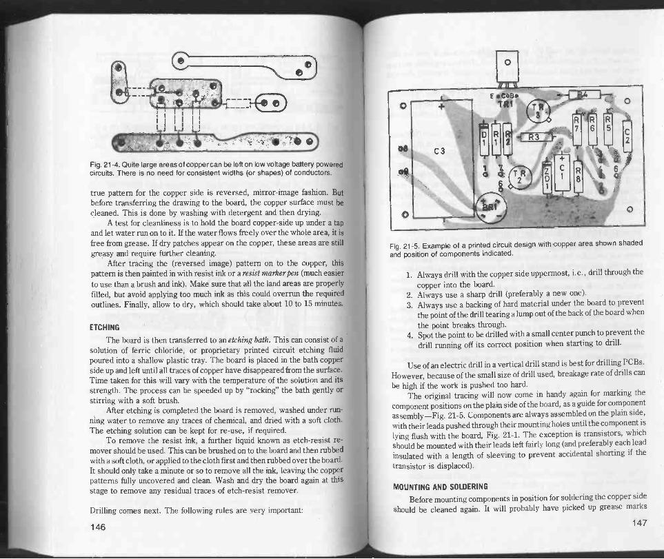
I
I
!`* 4!)
Fig. 21-4. Quite large areas of copper can be left on low voltage battery poweredcircuits. There is no need for consistent widths (or shapes) of
true pattern for the copper side is reversed, mirror -image fashion. Butbefore transferring the drawing to the board, the copper surface must becleaned. This is done by washing with detergent and then drying.
A test for cleanliness is to hold the board copper -side up under a tapand let water run on to it. If the water flows freely over the whole area, it isfree from grease. If dry patches appear on the copper, these areas are stillgreasy and require further cleaning.
After tracing the (reversed image) pattern on to the copper, thispattern is then painted in with resist ink or a resist marker pen (much easierto use than a brush and ink). Make sure that all the land areas are properlyfilled, but avoid applying too much ink as this could overrun the requiredoutlines. Finally, allow to dry, which should take about 10 to 15 minutes.
ETCHING
The board is then transferred to an etching bath. This can consist of asolution of ferric chloride, or proprietary printed circuit etching fluidpoured into a shallow plastic tray. The board is placed in the bath copperside up and left until all traces of copper have disappeared from the surface.Time taken for this will vary with the temperature of the solution and itsstrength. The process can be speeded up by "rocking" the bath gently orstirring with a soft brush.
After etching is completed the board is removed, washed under run-ning water to remove any traces of chemical, and dried with a soft cloth.The etching solution can be kept for re -use, if required.
To remove the resist ink, a further liquid known as etch -resist re-mover should be used. This can be brushed on to the board and then rubbedwith a soft cloth, or applied to the cloth first and then rubbed over the board.It should only take a minute or so to remove all the ink, leaving the copperpatterns fully uncovered and clean. Wash and dry the board again at thisstage to remove any residual traces of etch -resist remover.
Drilling comes next. The following rules are very important:
146
Fig. 21-5. Example of a printed circuit design with copper area shown shaded
and position of components indicated.
1. Always drill with the copper side uppermost, i.e., drill through the
copper into the board.2. Always use a sharp drill (preferably a new one).3. Always use a backing of hard material under the board to prevent
the point of the drill tearing a lump out of the back of the board when
the point breaks through.4. Spot the point to be drilled with a small center punch to prevent the
drill running off its correct position when starting to drill.
Use of an electric drill in a vertical drill stand is best for drilling PCBs.
However, because of the small size of drill used, breakage rate of drills can
be high if the work is pushed too hard.The original tracing will now come in handy again for marking the
component positions on the plain side of the board, as a guide for componentassembly-Fig. 21-5. Components are always assembled on the plain side,
with their leads pushed through their mounting holes until the component is
lying flush with the board, Fig. 21-1. The exception is transistors, whichshould be mounted with their leads left fairly long (and preferably each lead
insulated with a length of sleeving to prevent accidental shorting if the
transistor is displaced).
MOUNTING AND SOLDERING
Before mounting components in position for soldering the copper side
should be cleaned again. It will probably have picked up grease marks
147

through handling. An ordinary domestic powder cleaner is best for this,used wet or dry, and rubbed on with a soft cloth. The running water test canagain be used as a check for cleanliness, but if the board is wetted, dry witha cloth.
Components are normally soldered in place, one at a time, with theirfull lead length protruding. Excess length of wire is then cut off as close aspossible to the solder. Some people, however, find it easier to cut the leadsto length first, then solder.
Provided soldered joints are completed rapidly, in not more than about3 seconds, heat -damage to either the board or a component is If
the iron has to be held in contact with the lead for longer than this, thensomething is wrong with the soldering technique and heat damage couldresult, either to the component or by the lifting of the copper land on thePCB. The most likely causes of overheating are using an iron which is nothot enough or too small for the job; attempting to rework a soldered jointwhich has not taken properly; and trying to remove a lead which has beensoldered into the wrong hole.
SIMPLIFIED PRINTED CIRCUIT CONSTRUCTION
As a supplement to drawing-and for making neater straight lines-there are available rub -down transfer sheets of lines, bends, blobs forconnecting points, etc., which can be used to build up the required patternon the copper, supplemented with ink drawing where necessary. Thesetransfer symbols are resistant to etching fluid, so serve the same functionas drawn or painted lines, etc.
It is also possible to buy self-adhesive copper foil precut in the form oflines, bends, etc, similar to transfer strips, but which can be pressed downon to a plain panel to complete a printed circuit directly, without the need
for any etching treatment. Further shapes can be cut from self-adhesivecopper foil blanks. With PC boards made up in this fashion continuous
(conductor) sections can be made up from overlapping pieces, providedpositive connection is made by solder applied over the joint line.
148
Chapter 22
RadioRadio broadcasts consist of a radio frequency (rf) signal generated at a
specific frequency allocated to a particular station, on which is superim-
posed an audio frequency (aft signal.Only rf will work for transmission. The of part, which is the actual
sound content of the signal is, almost literally, carried on the back of the rf
signal, the two together forming what is called a modulated signal.
This combined signal can be produced in two different ways-amp-
litude, or up-and-down modulation, known as AM; and frequency modula-
tion (actually a very small variation in rf signal frequency about its station
frequency), known as FM.AM is the simpler technique and is widely used for long wave, medium
wave and short wave broadcasts. Broadcasting has always been referred to
in terms of wavelengths instead of signal frequency, until comparatively
recently. The relationship between wavelength and frequency is:
wavelengths (meters) - frequency, Hz
300, 000
300,000
frequency, Hz =wavelength, meters
(The figure 300,000 is the speed of light in meters/sec., which is the speed
at which radio frequency waves travel.)In the case of FM, very high transmitting
frequencies are used - and it
is generally referred to as VHF (very high frequency). Actual wavelengths
are very short, and so it is much more convenient to speak of frequency, the
usual range for FM broadcasts being 90-100 million Hertz (90-100 MHz). A
149

simple calculation will show that this means a wavelength of about 3.2 to 2.9
meters or say 3 meters.Regardless of whether the broadcast is AM or FM, though, any radio
frequency signal has the same basic requirement for receiving it. Thepresence of this signal has to be "found" and then sorted out from signalsfrom other broadcast stations. The "finding" device is the aerial, and the"sorting out" device is the tuned circuit, which together form the front end
of a radio receiver as shown in Fig. 22-1 (the extreme left-hand part of a
circuit diagram-see also Chapter 19).A tuned circuit consists, basically, of a coil and variable capacitor,
which can be adjusted to show resonance or maximum response to aparticular signal frequency applied to it. A full explanation of this behavior
is given in Chapter 7. All the broadcast signals reaching the tuned circuit
are very, very weak. Only that signal to which it is tuned is magnified by
resonance, so that it stands out at a very much higher level of signal
strength.An actual aerial wire connected to the tuned circuit may or may notbe
necessary. In the case of AM reception, the coil winding will also act as an
efficient aerial wire, if wound on a ferrite rod. This dispenses with the need
for an external aerial. The only disadvantage is that the tunedcircuit will be
directional, minimum signal strength being received when the ferrite rod is
pointing towards the transmitter sending the signal, and maximum signal
strength when the ferrite rod is at right angles to this direction. This effectis most noticeable on small radio receivers which have only moderate
amplification. To receive certain stations at good listening level, even with
maximum adjustment of volume, it may be necessary to adjust the position
of the set. Larger receivers normally have enough amplification to compen-sate for this, but the effect can still be quite noticeable. Also, it is alwaysbest to operate a receiver below maximum amplification because this
minimizes distortion of the signal.
Iaerial
coupling capacitor to minimise effectof aerial capacitance on tuned circuit
Coil
variable capacitor
tuningcapacitor
coil woundferr to rod
Fig. 22-1. A variable capacitor and coil form the usual tuned circuit. Strictlyspeaking this tunes the aerial, if an external aerial wire is used. Most AMreceivers use a ferrite rod aerial which does not require an external aerial.
150
The FM receiver does need an external aerial because a wound coil or a
ferrite rod aerial just will not work at this rf. For satisfactory results, this
external aerial also needs to be a special type, known as a dipole, which
itself is "tuned" by making its length one half of the signal wavelength. The
latter may vary from 11.5 ft. to 9.5 ft. in the 90-100 MHz FM band, so a
mean wavelength figure of about 10 feet is adopted, giving a realistic dipole
length of 5 feet.The three practical FM aerial forms are a vertical telescopic aerial
extending to 30 in. ; a horizontal wire (or rod aerial) with 30 in. "legs"; or a
folded dipole, as shown in Fig. 22-2.
5 feet
I.-
dipole aerial
5 feet
70-75 ohms impedancematching feeder cable
folded dipole 280-300 ohms impedancematching feeder cable
Fig. 22-2. FM aerials need connecting to the set via a correctly matched feeder
cable.
DETECTION
The tuned circuit is much simpler than the foregoing descriptions may
appear to imply. It is really a matter of getting the component values right,
and working with high efficiency (see also Chapter 6 and Q -factor). Design
of the tuned circuit is a little more complicated when a radio is intended to
receive more than one waveband. Even an AM receiver needs separate
aerial coils (or at least separated wings on a single ferrite rod) to cover long
wave, medium wave, and short wave. So the tuned circuit design for an AM
receiver could involve three or more tuned circuits selectable by a switch.
In the case of an FM receiver (or the tuning circuit for the FM section
of a multi -band receiver), there is really no practical form of wound aerial
coil which can be used (a theoretical coil of this type would probably require
only a part of a single turn). So the starting point is a dipole aerial. This
itself is a tuned circuit (i.e., designed to be resonant with the mean
frequency to be covered in the FM band), but its amplification of signal will
not be anything like as good as that of the coil -and -capacitor tuned circuit of
an AM receiver.To compensate for this, the FM receiver normally uses an amplifier
stage immediately following the aerial, known as a preamplifier or rf
151

amplifier (because it is an amplifier of signals at radio frequency).amplified signal is fed to the next stage of the receiver via a tuned output,.typical circuit of this type being shown in Fig. 22-3.
tuningcapacitor
Input from dipole aerial
F7outputto mixer
rf transistor
Fig. 22-3. Basic rf amplifier (or preamplifier) circuit as used in most FM receivers.
The detector stage following the tuned circuit can be extremely simple.In the case of AM, it only needs to be a diode connected to a potentiometeras its load. This potentiometer also acts as the volume control - Fig. 22-4.
The signal passed on from the tuned circuit to the detector is astrengthened version of the original modulated broadcast signal. In otherwords, it contains both af and rf. The rf part has now done its job in gettingthe signal into the tuned circuit. Now it needs to be removed, which can bedone by rectifying the signal. A diode does this job by "chopping off" onehalf of the rf signal so that the output from the diode consists of half -cycles ofrf. These half cycles have the af content of the signal still imposed, so thenext requirement is to filter out the rf part to turn the output into anundulating dc signal. These undulations follow exactly the same variationsas the af signal originally imposed on the transmitter rf signal at thetransmitting station by a microphone, or recording.
As explained in Chapter 6, a resistor and capacitor can act as a filter forany specific frequency required. Thus the diode detector is associated with
a matching load (resistance) and associated capacitor forming the requiredfilter circuit, e.g. see Fig. 22-4 - so that only varying dc is passed at outputfrom the detector stage. It is usually coupled to the next stage by acapacitor, which has the further effect of balancing the varying dc signalabout its zero line (i.e., giving it positive and negative values, rather than"all positive values").
In practice, the output load (R in Fig. 22-4) is usually a variableresistor, which component then also acts as a volume control. The fact thatthis is followed by a coupling capacitor also avoids any flow of dc through themoving contact (wiper) of this control and reduces any tendency to repro-duce "noise" by movement of this control.
The aim in selecting the detector circuit components is that the signalpassed by the diode is exactly the same as the original signal generated by
152
the studio microphone (with certain losses and possible distortions!). Fed
to a microphone working in reverse (i.e., headphones or a loudspeaker)
they would be heard as the original speech or music, etc. But the signals at
this stage are still too weak to have enough power to drive headphones or a
loudspeaker, so the next step is to amplify the af signal passed by the
detector.
rf + of signal
capacitor to filtercut residual If onsuperhets
I
0+
coupling capacitor helpsto eliminate 'noise' from volume control
IIFig. 22-4. Basic AM detector circuit.
volume control
af output
FM DETECTOR
In the case of an FM receiver, the detector is a little more complicated.
It has to detect how the frequency of the signal is varying, not its amplitude,
so it has to extract the original frequency as well as apply rectification. FM
receivers invariably work on the superhet principle, so the frequency to be
extracted is the intermediate frequency or i-f. A basic detector circuit
employs a three -winding transformer with primary and secondary tuned to
the intermediate frequency (by capacitors Cl and C2 in Fig. 22-5). The
third winding injects a voltage into the secondary circuit, each leg of which
carries a diode, D1 and D2, associated with a capacitor C3 and C4.
The working of this circuit is to detect variations in signal frequency in
pri mary
Fig. 22-5. Basic FM detector circuit.
153

r.
terms of an af output, so that the final output is exactly the same, in terms ofsignal content, as that from an AM detector. Thus it can be dealt with in thesame way. The additional components R1 and C5 shown on the diagram areto suppress unwanted signals which may be present after detection.
AMPLIFIER STAGES
A single transistor can provide amplification of signal strength up to100 times or more (see Chapter 9 for typical amplifier circuits). The mainrequirement of the amplifier following the detector is that the transistor bespecifically suitable for amplifying af (when it can act as a further block toany residual rf remaining in the input signal to the amplifier). Ideally, thereshould be no rf signal present at the input to the amplifier stage (it shouldhave been filtered out in the detector stage), since any rf voltage presentedto the amplifier stage could cause overloading.
Theoretically, at least, any amount of amplification can be produced byadding additional transistor -amplifier stages (Fig. 22-6). This does, how-ever, greatly increase the chances of distorting the signal, so there arepractical limits to the number of stages which are acceptable in simplecircuits. Much better results can be produced by more sophisticated cir-cuits, particularly the superhet (see below), where first some intermediatesignal is amplified before detection; and subsequently amplified again afterdetection.
Fig. 22-6. Adding amp ifier stages is not necessarily a good thing for amplifyingan af signal as each stage can amplify distortion produced in the previous stage.
OUTPUT STAGE
The af amplifier output (or last af amplifier stage output if more thanone stage is used) can develop enough power to drive a loudspeaker, as inFig. 22-6, although there may be some problem in matching the (amplifier)output to the (loudspeaker) input, particularly using low .to medium powertransistors which require a high impedance load to match. Most loudspeak-ers have a load impedance of only 4-16 ohms. A basic solution here is to usean output transformer to match the different load characteristics, as in22-7.
This relatively simple solution does, however, have one particularlimitation (for the more technically minded, it is called a Class A output). It
154
af signal input
impedance matching-I transformer
Ecoupling capacitor
output transistor
class A amplifier
Fig. 22-7. Basic Class A output circuit.
is relatively inefficient and so draws a high current in providing a suitable
listening level from the loudspeaker. It is satisfactory for use in car radios,
but represents too heavy a current drain for most other battery -powered
receivers.These normally use a Class B output circuit where the last amplifier
transistor drives a pair of transistors which effectively work in a push-pull
circuit operating the loudspeaker. The output power obtained is consider-
ably more than double the power available from a single transistor; also,
and output transformer is not necessary. Most modern af amplifiers for
radios end up in a push-pull output stage of this type, like the circuit shown
in Fig. 22-8.The limitations of simple radio receivers are mainly connected with
the limitation of a detector. A detector is most effective working with an rf
input voltage of 1 volt or more. Signals derived directly from an aerial
circuit are seldom more than a few millivolts in strength, and the weaker
the signal the less effectively they will be detected in any case. In other
words, the range of stations that can be picked up is limited, and no amount
of amplification after detection can make up for this limitation.
This limitation, or lack of sensitivity can be overcome by amplifying the
incoming signal before detection, so that the detector is always working
with good signal strength. This can be done by rf amplification of the aerial
signal by introducing an amplifier stage right at the beginning of the circuit
as in the FM receiver (Fig. 22-3); or by the superhet working. The latter
also improves the selectivity of a receiver, or its ability to tune in sharply to
wanted signals and reject nearby station signals.
THE SUPERHET
Having arrived at a standardized output stage, it is equally true to say
that nearly all modern radio receivers are of the superhet type, which is
considerably more complicated than the circuit traced through above. The
whole "front end" works on an entirely different principle.
155

Couplingcapacitor
decouplingcapacitor
this resistordetermines feedback
TRI
quiescentbiasresistor
TR3
decouplingcapacitor
, TR2Cglirsristor)
TR4
O+
Fig. 22-8. Basic Class B output circuit. TRI works as a preamplifier. TR2 is thedriver. TR3 and TR4 are a complementary pair of transistors, working alterna-tively in "push-pull." The two resistors shown by dashed lines may be added toimprove the stability of the circuit. These only need to be of very low value (e.g., 1
ohm).
Starting point is the tuned circuit (ferrite rod aerial) in the case of anAM receiver; or a dipole aerial feeding an rf amplifier in the case of an FMreceiver (the latter amplifying the modulated radio signal in conjunctionwith a tuned resonant circuit). In both cases the boosted tuned signal is fedto an oscillator -mixer.
This is a two -function circuit, although its duty is usually performed bya single transistor associated with a tuned oscillator circuit. This tunedcircuit is mechanically coupled to the aerial tuning in the form of a gangedcapacitor (i.e., two separate variable capacitors coupled, or "ganged" tomove together when the tuning control is adjusted), so that it "tracks" theaerial circuit tuning while remaining separated from it by a constant fre-quency. This difference is known as the intermediate frequency or i-f, and isusually 455 kHz above the aerial frequency (it can have other values incertain sets ; and can also be below rather than above the aerial frequency).
The oscillator part of the oscillator -mixer is concerned with generat-ing this fixed intermediate frequency, tracking exactly above (or below) thesignal frequency to which the aerial circuit is tuned. The two signals arecombined in the mixer part of the oscillator -mixer, which also has a fixedtuned circuit (actually the primary side of a' transformer associated with a
capacitor) which responds only to the intermediate frequency - Fig. 22-9.This i-f signal also now has the same af modulation as the original signal. Inother words, it is a duplicate of the wanted af signal, but at this stagesuperimposed on a fixed intermediate frequency.
There are a number of technical advantages to this seemingly un-necessary complication of incoming signal treatment. First, the process of
156
amp
separate amplifier stages
amp amp amp
Fig. 22-9. Front end of a superhet receiver, showing how the incoming rf plus af
signal is transformed into an af signal now imposed on a fixed intermediate
frequency (i-f). This makes amplification without distortion more simple to
achieve.
superheterodyning gives much better selectivity or rejection of unwanted
signals. Then, the signal outputfrom the mixer is at a constant frequency,
making it easy to amplify with the further possibility of eliminating any
remaining unwanted frequencies since an i-f amplifier has fixed-and virtu-
ally exact-tuning.In practice, i-f amplification is usually carried out in two stages (AM
receivers) or three stages (FM receivers). The detector then follows after
the i-f amplifier stages-Fig. 22-10. Each i-f amplifier stage consists of a
tuned transformer, adjustment of tuning being done by an iron dust core in
the transformer coil former. Once correctly adjusted, in setting up the
receiver for proper working, no further adjustment is necessary, or made.
The cores are sealed in this position.The remainder of the radio circuit follows as before -rf amplifier
stage(s) following the detector, terminating in (usually) a push-pull output
stage. But there is just one further refinement which can be added. By
feeding a proportion of the signal passed by the detector back to the first i-f
amplifier stage, automatic volume control (normally called automatic gain
control or agc) can be achieved. If the signal strength passed by the detector
starts to rise to a point where it could become distorted, then feedback via
the agc line automatically reduces the amount of signal entering at this
point, so maintaining the detector working under optimum conditions.
Agc applies only to the control of amplification of signal in the i-f
FM aerial(dipole)
rfamplifier
Liosci Iletor-mixer
AM eerie!(ferrite rod)
let ifsimplifier
AMdetector
FMdetector
Fig. 22-10. Basic design of an AM/FM receiver shown in block form. The only
common circuit is an af amplifier (usually a Class B output) following the detec-
tors.157

amplifier stages. The output or gain of the final i-f amplifier stage(s) isgoverned by a separate volume control (potentiometer), typically locatedbefore the first of amplifier stage. This potentiometer, incidentally, usuallyhas a capacitor connected in parallel with it to filter out any residual i-fwhich may have got past the detector.
158
Chapter 23
TelevisionTelevision makes special use of a cathode ray tube, which in turn has certain
characteristics in common with a vacuum tube (see Chapter 12). It has a
heater, a cathode which emits electrons, an anode to which electrons are
attracted, and a control grid. Unlike a tube, however, the electrons are
directed at the enlarged end of the tube or screen which is coated with a
Phosphor material.It is, in fact, a special type of cathode ray tube. The narrow end of the
tube acts as an electron "gun," shooting electrons past the anode section.
Electrons impinging on the screen generate more electrons which are
attracted back to the anode, equivalent in effect to each electron reaching
the screen being bounced back to the anode. Thus no electrons, and hence
no charge, actually collects on the screen. Meantime, however, each
electron reaching the screen makes the phosphor glow, which glow persists
for a short period after the electron has been "bounced back."
The brightness of the glow produced is dependent on the type of
phosphor (which also governs the color of the glow), and the strength of
bombardment of electrons. The latter is controlled by the bias voltage
applied to the grid. In other words, grid bias adjustment is the brightness
control on a TV tube, Fig. 23-1. The actual brightness is also enhanced by
an extremely thin layer of aluminum deposited over the phosphor to act
rather like an outward -facing mirror, but transparent from the other side as
far as electrons are concerned.To produce a picture from electron bombardment, two other controls
are necessary. The first is a means of deflecting the electron beam so that a
single spot can trace out a particular path covering all the variations in
picture density over the whole screen area. The second is a means of
159

cathode
grid
brightnesscontrol
anodes
focuscontrol
deflection plates
aluminizedlayer
Fig. 23-1. The TV tube and its basic controls, shown in simplified form.
focusing the electron beam into a tiny spot so that the traced picture issharp, not fuzzy.
Deflection is achieved by directing the stream of electrons through twosets of parallel coils set at right angles to each other like the X and Ydeflection plates in a simple cathode ray tube (Chapter 12). Signal voltagesapplied to the X -coils will deflect the beam sideways; signal voltagesapplied to the Y -coils will deflect the beam vertically. Combined X and Ysignals will thus direct the beam toward any spot on the screen, dependingon the resultant effect of the two signals.
Focusing, meantime, is achieved by using supplementary cylindricalanodes arranged to work as an electronic lens, with the focusing effectadjustable by varying the voltage applied to one (or more) of these anodes.These anodes come before the deflection plates, i.e., in the parallel or"gun" section of the tube rather than in the divergent section.
Electronic circuits can respond very rapidly - which is how televisioncan be made to work at all! To "paint" a picture on the screen a spot of light(produced by a focused electron beam) has to traverse the whole picturearea, zig-zag fashion, at least 30 times per second if the picture is to appearreasonably free of flicker. It does this in a number of parallel lines, usuallyrunning from left to right, with rapid "flyback" between lines, Fig. 23-2.The greater the number of lines the clearer the picture will be, i.e., thebetter the definition. The standard commonly adopted is 525 lines (perpicture). So the actual frequency at which lines appear, called the linefrequency, is 30 x 525 = 15750 per second. This line pattern is known as araster. The lines making up the raster can actually be seen if you examinethe television screen close up, or turn up the brightness control when no
160
picture is being transmitted. Only the parallel lines will be seen in the
raster. During flyback, the cathode ray tube is cut off and no lines appear on
the screen.In practice the picture is scanned 60 times per second, not 30. This is
fast enough to eliminate any trace of flicker, but using an optical "trick," the
actual picture frequency is still only 30 per second. Scanning takes place in
two stages - first the odd lines only, then the even lines. Each scan
therefore builds up only half the picture, the two halves following each
other to present the complete picture.Movement of the lines downwards is accomplished by the time base
circuit starting with the first (odd) line and restarting a line at the left two
positions down each time. This continues until the scanning has reached
525 ÷ 2 = 262% lines. The spot then flies back to the top again, starting half
way along the first even line and repeats the process to scan the 262% even
lines which make up the second half of the picture. This process is known as
interlacing. Actually a few lines get left out in this changeover process, but
this does not show up on the picture.Picture transmission and picture reception operate in reverse mode.
The television camera scans the scene to be transmitted in 525 lines at a
picture frequency of 30 per second, and turns the light spot response into
electrical signals. The number of lines has been quoted as governing
picture definition, but this is not the whole story. A scan of 525 lines gives
good picture definition from top to bottom, e.g., the picture is built up
top -to -bottom from 525 "strips." There is also the question of how many
Start
3
5
7
9
r
-r
I
4
.111.*
a.* 6
8
10
Fig. 23-2. Illustrating the formation of a raster. First the odd number lines are
scanned from left to right (solid lines) with flyback between each line (dashed
lines). Downward movement is controlled by the time base. After scanning half
the picture lines, the time base flies back to the top. All the even number lines are
then scanned, with "flyback" between each line (right hand diagram). At the end
of the last line the time base flies back to top left to start the sequence all over
again. These two diagrams superimposed would represent a complete raster.
161

individual picture elements are covered by each strip. The answer is about600 as an absolute minimum for good picture definition side -to -side, or theequivalent of 600 phosphor "dots" making up each line. The total number ofindividual "dots" or picture elements in each whole picture trace is thus315, 000. Since the picture frequency is 30 times per second, this calls for atransmitted signal frequency of 2.5 MHz.
These "intelligence" signals are broadcast like any other radio trans-mission-superimposed on a carrier wave to produce a modulated signalwhich can be picked up by a receiver and decoded on a similar principle toordinary radio reception, except that the decoder now has to handle radiofrequencies of 2.5 MHz and not of signals, so the TV receiver decoder isconsiderably more complicated than a radio receiver detector.
There is also another important difference. Carrier wave frequencieshave to be much higher than modulation frequencies for satisfactory re-sults. Hence the frequency of television picture signals is in the VHF range.It is invariably an AM broadcast with sidebands, operating within a channelwidth of 8 MHz. Either AM or FM can be used for the accompanying sound
signal, FM being standard.The fairly wide channel width or frequency spread occupied by a
television transmission does not make it susceptible to receiving spurioussignals upsetting the picture (but not the sound, which is operating in a
narrow band like any ordinary FM receiver). It also limits the number oftelevision stations that can be accommodated in the VHF band withoutinterfering with each other.
This particular consideration also makes the design of a color televi-sion system even more complicated than it need be using first -principleelectronics. For example, it would mean expanding the bandwidth to threetimes its black -and -white figure to transmit three separate pictures simul-taneously in the three primary colors. Since this is not an acceptablesolution, color information has to be contained within the 8 MHz channel
allowed for black -and -white transmissions, which becomes an extremelycomplicated subject and virtually impossible to describe in simple terms.Strangely enough, however, it does simplify ne other problem-the essen-tial requirement that a color television should also be able to receiveblack -and -white transmissions in black and white. The broadcast stationsstill have the opposite problem of ensuring that color transmissions can be
received on black -and -white sets in black -and -white!The conventional color TV tube is made with three guns, one for each
color-red, green, and blue; with each dot on the screen formed byseparate red, green, and blue phosphors arranged in a triangle. The pictureis thus scanned by a triangle of beams converging on each triangle of dots atthe same rate as in a black -and -white picture. The resulting sharpness of
the color picture depends primarily on the accuracy of convergence, and onsome tubes may vary noticeably from center to edge and/or top to bottom.This may be a limitation of that particular design of tube and associatedcircuitry, or merely a matter of convergence adjustment (which is usually
factory -set and can be quite complex). There are improvements in this
respect in the case of some modern tubes, e.g., simplifying convergence
problems by using in -line guns and color spots.
163
162

Chapter 24
MicroprocessorsThe years 1939-45 saw the development of analog and digital computingtechniques, and, towards the end of that era, the first appearance ofelectronic computers based on tubes and relays. Years 1948-50 saw digital
computers established, using tubes and-more significantly-the de-
velopment of the transistor.Ten years later (1960), printed circuit boards first appeared, and also
the first small-scale monolithic integrated circuits and hybrid integratedcircuits. Transitional computer circuits took over from tubes. Medium -
scale integrated circuits (MSI) appeared in 1965, and large scale integratedcircuits (LSI) in 1970. Throughout this period of rapid development of ICs,
aspects of digital computing were further extended, culminating in theappearance of the first micro-miniaturized computer, or microprocessor, in
1971. From that date, there has been intensive development of digital
integrated circuits in micro -miniature form through DTL to TTL to MOS-
FET and CMOS, etc. Throughout this period, the capabilities of micro-
processors have continued to be improved, with, most significant of all, a
fall in prices.Essentially, the microprocessor is a digital computer in micro -
miniaturized form, but not necessarily with the full capabilities of a conven-
tional digital computer. One of its main applications, in fact, is a Program-
mable Controller (PC) for various industrial applications. Within the last
five years or so, upwards of 60 different PC systems have appeared,designed for industrial use, as well as others with more open capabilities.Each is associated with its own peripheral devices and associated software
(i.e., programming devices).Originally, PCs were designed as one -bit processors, using discrete
164
components. Today, they are invariably based on microproces-
sors, or, in some cases, combinations of both a microprocessor and a
one -bit processor. Some of the more recently introduced types incorporate
dual -language processorsbased on bit -slice technology.
One of the most important features of a microprocessor is its size -
not its physical size, but the length of the data word it operates on and the
number of words its memory can store. Microprocessor lan-
guage is measured by the number of bit per word, a bit being a binaty
Common microprocessorword lengths are 4, 8, 12, and 16 bits. An 8 -bit
data word is by far the most common, and is given a special name-a byte.
Because there are only two possible combinations for one bit, it
follows that the total number of combinations possible in a binary word in a
given length is 2 raised to the Nth power, where N is the number of bits in a
word. Thus, for an 8-bit word, the total number of combinations is 28 - 256.
As one measure of microprocessor size is the length of its word, this
reflects on the size of the memory. The memorymust be able to store a
given number of words of this length. For example, a byte -oriented micro-
processor with a memory that can store up to 10 words will have 80 bits of
storage capacity in the memory. It is generally assumed that a 4 -bit
microprocessor is accompanied by a memory storing 4 -bit words, and a
16 -bit microprocessor with 16 -bit words of memory.
It follows, therefore, that memory size is measured by the number of
words it may store. Often, the IC which is referred to as a microprocessor
has little or no memory; the memory for the unit is contained in other ICs.
The maximum memory capacity of a PC system depends on the
addressing capability. But, in practice, the maximum expandability is
related to the maximum physical number of inputs and outputs, and also of
the complexity of control algorithms. A rule of thumb for calculating
memory requirementsis: 10-15 instructions (or commands) per one output
on the average application for sequential control, with few arithmetic,
timing, or counting functions. For applications with a more sophisticated
control algorithm, 15-20 instructions per output may be required. You have
to consider more memory space if several programs are to be stored
simultaneously, which are selectable by a manual operation mode switch,
for example, for frequently changing production at one machine. The
maximum memory capacityof PCs on the market ranges from 256 words
(one word corresponds to one instruction) to 16000 words (commonly
expressed as 16 K) and more. Memory systems are modular and expandable
from a minimum "starter set" of 1/4 k in increments of V4 k, 1 k, and 4 k.
In simple form, the microprocessor comprises three basic parts: the
central processing unit (CPU), memory, and the I/O devices. A micro-
processor always contains a CPU, and in some instances, memory as well
as an I/O device. The CPU has the ability to send (address) information to
either the memory of the I/O device (see Fig. 24-1).
Just as the memory must have an address before data may be trans -
165

Programmer 1--
r---- -1I Programmer II Downloader 1<-II
Programmable controller
Processor
Ladderelementstorage
Inputs X
Flags C
Outputs Y
Power flow
- Push down_ stack
-0-
Inputr i eld
devices
Outputfielddevices
Fig. 24-1. Block diagram of Texas 510 Programmable Controller.
ferred to or from it, so much the I/O devices. Normally, there is more thanone input or output device on a system. Therefore, the CPU must decidewhich one it wishes to transfer data with, and this is done by addressing.
To execute a particular program, the programmer may set aside acertain area of the memory for program storage. Other areas of memorymay be set aside for data storage, and these assignments may change for adifferent program. The Texas 510PC, shown in schematic form in Fig.24-1. is one of the latest types of programmers on the market, and illus-trates the position of the microprocessor within the total package whichincludes memory storage, location area, image register (IR) and push -downstack (PDS).
All entries to the sequencer are made with a plug-in programmer. Thiscan read out and modify all locations within the memory storage locationarea. When an entry is made, it is entered into and stored within thisstorage area. Timers and counters as well as series and parallel logic arecontained therein.
The processor controls the Model 510 PC memory during program-ming and execution of the user program. Logic instructions from theprogrammer are entered into the storage area (user memory). At the startof each program scan, the processor places the status of the instruction inthe register and transfers the status of the selected output to the output (Y)lines.
I/O modules are commonly available as plug-in cards or plug -on boxesin increments of 2, 4, 8, 16, and 32 lines per module. However, 8 -stagemodules and 16 -stage modules seem to be the best buy. A broad variety ofI/O cards with different signal -voltage levels are available from many
166
manufacturers. Types of I/O modules are: 5 Vdc Transistor -Transistor
Logic (TTL); 24 Vdc; 48 Vdc; 120/24 Vdc; 24 Vac; 120/24 Vac, etc.
In practical application, however, preference should be given to one stan-
dard signal voltage,thus faulty I/O modules can be replaced by a spare I/O
module of the same type.Swapping I/O cards is a fast, sure, trouble -shooting technique. Where
possible, control elements and I/O modules of the same signal type should
be used, which means inexpensive I/O modules of the same signal type
should be used, which means inexpensive stock of spare components. The
output current load per line of various output cards ranges from 0.5A to 2A,
but some PCs on the market may have a problem - namely, not all outputs
on a card can be energized simultaneouslybecause the card does not have
the current -carrying ability to energize all outputs at once. The maximum
number of inputs/outputs per system ranges from 32 for small, 128 for
medium, and up to 4096 for large systems. However, at this point, it must
be noticed that a large number of inputs/outputs, as well as corresponding
large programs, may heavily reduce the response, or cycle, time of an
application. The distributed systems concept may be more appropriate for a
large and complex application.Several larger PCs have some capabilities or options which allow
continuous process control with algorithms built-in for standard PID
(Proportional -Integral-Differential) controllers with analog inputs and out-
puts. The combination of logic control and analog loop control means that
these PCs can be used for batch or continuous processing applications;
however, they are not able to completely replace typical process -loop
controllers. Usually, loopcontrollers are built as plug-in or plug -on mod-
ules for extended PC systems. Optional available ADC (Analogue -to -
Digital Converters) accept, respectively supply signalsof 4-20 mA or
0-5/0-10 Vdc. The signal resolution is rather low. Precise measurements
are not possible at typically three -digit BCD (Binary Coded Decimal) value.
Counter and timer functions are indispensable tools of a PC system.
Nominally, up to 64 internal counters or timers are built into medium to
large-scale PCs. The time base is generated through a quartz oscillator
clock that can commonly deliver three different time standards: 0.1s, 1.0s,
and 1.0 min. Three -digit cascading up-and-downcounters and timers pro-
vide convenient tools for a wide range of applications. For fast counting
applications, such as positioning or angle -indicating transducers, separate
fast counter cards are necessary. A critical specification for using internal
counters is the counting frequency under the worst -case timing conditions,
because the actual count -rate depends very much on how the program is
structured; therefore, special attention must be paid to timing-related
problems.
167

Chapter 25
BatteriesBatteries may be divided into two main groups: primary batteries, wherethe electrochemical action is irreversible (once the battery has been dis-charged it cannot be reenergized); and secondary batteries, where the
electrochemical action is reversible and they can be charged and dischargedrepeatedly (but not indefinitely), to be used over and over again.
Primary batteries are popularly called dry batteries; and secondarybatteries are called storage batteries. These descriptions are not strictlycorrect, but they are convenient and widely accepted. In fact, all primarybatteries have some form of "wet" electrolyte (usually in the form of a pasteor jelly); and many secondary batteries may have so-called "dry" cells
(implying the use of a non -liquid electrolyte). And just to show how generalclassifications cannot always be strictly correct, some types of primary(non -rechargeable) battery systems are, in practice, rechargeable!
DRY BATTERIES (PRIMARY BATTERIES)
A battery is made up of one or more individual cells. Each cell willdevelop a specific nominal voltage, depending on the battery system. To
build a battery with a higher voltage than that given by a single cell, two ormore cells are connected in series.
The nominal cell voltage given by different "systems" is:
(i) carbon -zinc - 1.5 volts(ii) alkaline -manganese - 1.5 volts(iii) mercury - 1.35 or 1.4 volts (depending on the depolarizer
used)(iv) silver oxide - 1.5 volts(v) zinc -air (a comparatively undeveloped system as yet) - 1.2
volts
168
Choice of the best "system" is dependent on cost and utilization of the
battery. Carbon-zinc dry batteries are by far the most popular because they
are relatively cheap and readily available in a wide range of voltages and
sizes, the latter governing the capacity of the battery, or the amount of
electrical energy it can store.Typical construction of a carbon -zinc cell is shown in Fig. 25-1. Higher
voltage dry batteries may be produced by connecting two or more cells in
series in a suitable pack, or more usually, by employing layer type con-
struction, as shown in the second diagram.The two main disadvantages of standard carbon-zinc cells (or bat-
teries) are:
1. Under load (i.e., when current is being drawn from them), they are
subject to a build-up of internal resistance due to "polarization,"
which has the effect of causing the output voltage to drop. The more
rapid the rate of discharge, the more pronounced this voltage -drop
effect.
KEYA Brass CapB Manganese Dioxide
DepolarizerC Zinc Case
(Negative Plate)D Ammonium Chloride
ElectrolyteE CardwasherF Carbon Rod
(Positive Plate)
KEYA Metal Top CapB Plastic Top CoverC Carbon RodD Soft Bitumen Sub -seal
E SealF Tamping WasherG DepolarizerH Paper LiningJ Zinc CupK Paper TubeL Metal JacketM Bottom PaperN Metal Bottom Cover
Fig. 25-1. Standard carbon -zinc cell (left) and HP cell (right).
169

2. The outer zinc case (normally enclosed in a paper or plastic jacket)is continually being eaten away by chemical attack, which acceler-ates as the cell becomes more and more discharged. If the battery isleft in a flashlight, radio, battery -holder, etc, and left in a near -discharged or discharged state, the zinc casing will soon be eaten
right through, allowing corrosive electrolyte to escape.
To a large extent, this can be avoided by using leakproof constructionwhere the zinc case and cell bottom are enclosed by metal covers (usuallytinplate). Even the leakproof carbon -zinc battery can suffer casing failureand leak if left in place when discharged, however, for there is always atendency for the contents of the cell to swell and burst the casing when the
cell is in a discharged state.The high power, or HP, cell is an attempt to overcome both limitations.
It is invariably of leakproof construction and also employs a more effectivedepolarizing agent. As a result, it has a superior performance under highcurrent drains, and also increased capacity. It is also more expensive, so
Table 25-1. Standard Carbon -Zinc Batteries (up to and including 9 volts).
Type*
Size (millimetres) Recommended
Nominal Weight Length or current range
voltage (gr) diameter Width Height (mA)
U12(Penceli)0118P11HP11U28P2HP2AD4FLAG
1839
PP11126AD2B481
PP1
PPS996991
PPSPP4PPGPP7PP9PP10PP11
1.5
4.5
25 14 34545 2645
90990
34
600 67880 67
3 26
65103100113
450370450
1130
283 651100 66580 67
1500 136
38 26.851 25 4
142 369 200 46
425 66
1250 65
459 65
6
67
52 5353566
56526772
17,5
3546525252
50 20-3020-60
50 20-600-1000
10-5060 10-50
0-2000102 100-250166 100-250
100 20-60
9191
106165
10-1000-250
30-300100-250
56 5-50200 20-150102 30-300125 30-500
4850706281
22591
0-100-10
2.6-155-205-50
15-1505-50
Type numbers shown in bold are World standards. Other typesReady. See Table 25-2A and B for equivalents.
170
numbers are Ever
an HP cell is not always a "best buy." In fact, the additional cost of HP cells
is really only justified where the current drain is higher than that recom-
mended for standard carbon -zinc cells. And if positive leakproof perfor-
mance is essential, another system is better (in particular, alkaline -
manganese).Table 25-1 is a useful guide both to the nominal voltage of standard
sizes of carbon zinc batteries and their recommended operating range in
terms of current drain. Capacities cannotbe quoted for carbon -zinc dry
batteries since the capacity of a particular size and type of cell can vary
widely with different current drains, and the actual operating cycle. This
capacity-or battery life-can really only be determined by practical
experience in that particular usage.
ALKALINE -MANGANESE CELLS
Construction of a typical cylindrical alkaline -manganese cell is shown
in Fig. 25-2. They are generally available only as single (1.5 volt) cells, and
ABCD
E
F
GHJ
KL
M
KEYA Inner Steel Case
and Positive TerminalB Outer Steel CaseC Insulating DiscD Insulating SpacerE Absorbent SleeveF Electrolyte in
Absorbent MaterialG Zinc Anode CylindersH Depolarizer CylindersJ Electrolyte ImmobilizerK Sealing and
Insulating GrommetL Steel Double Plate
Negative TerminalM Battery Jacket
Fig. 25-2. Typicalconstruction of a modern alkaline -manganese cell.
in a much more restricted range of sizes (see Table 25-2). They are
considerably more costly than carbon -zinc cells, but have three main
advantages:
1. Voltage drop under load is far less pronounced.
2. They have a long, almost indefinite "shelf life" (i.e., there is
virtually no loss of capacity in storage with fresh cells, and even
with partly -discharged cells).
3. They have far more capacity for the same size compared with
carbon -zinc cells, and thus a longer battery life under similar
working conditions (size for size, about six times that of a standard
carbon -zinc cell).171
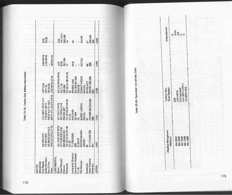
Tab
le 2
5-2A
. Car
bon
-Zin
c B
atte
ry E
quiv
alen
ts
UN
ITE
DK
ING
DO
ME
ver
Rea
dyE
xide
(D
ryde
x)R
ay -
O -
Vac
Vid
or
U2
HP
2 S
P2
T2
SP
2 H
P2
D2
RR
13 2
LP H
C2
HP
2 V
2 LP
V2
VT
12
U11
HP
11 S
P11
C11
T15
SP
11 H
P11
RR
14 1
LP C
1 H
C1
HP
11 V
11 L
PV
11 V
T13
HP
7 D
14H
P7
T5
7R R
R15
V12
HP
14 V
T14
U16
HP
16U
16 H
P16
HP
16 V
16
D23
DL3
3
CO
NT
INE
NT
AL
Ber
ecU
2 LP
U2
SP
2 P
P12
U11
SP
11 P
P13
U7
U12
PP
14 P
P15
U16
D23
Cip
el (
Maz
da)
GT
1 F
20 P
20 L
F20
MT
1 R
FM
LF
14A
C1
LF6
RF
BP
A1
PC
1D
aim
on25
3 28
9 25
0 25
125
8 25
9287
2982
9629
1 29
429
2 29
5H
elle
sens
VII
-33
VII
-34
V11
-36
VII
-24
VII
-25
V11
-26
VII
-28
VII
-38
VII
-75
1714
VII
-37
VII
-27
18Le
clan
chii
(Fra
nce)
T1
R20
R2O
SR
14 R
14S
R6
R6S
HA
6R
O3
R1
Lecl
anch
e (S
uiss
e)20
820
7 60
420
1 20
2 60
1 60
2P
. L.B
.E
2 E
4 E
7E
5E
15 E
18P
ile W
onde
rE
XP
OR
MA
RIN
BA
BIX
JU
NO
NS
ON
AT
VE
BE
RE
XT
AZ
SA
FIR
AM
IRO
ES
CA
LN
AV
AL
Sup
erpi
la60
6163
433
AC
768
67V
arta
(P
ertr
ix)
211
212
222
232
214
235
236
213
233
2442
5129
4280
239
245
249
Witt
e K
at66
766
866
666
5JA
PA
NU
M1
UM
2U
M3
UM
4U
M5
Alk
alin
e -M
anga
nese
(Mal
lory
)
Mn-
9100
Mn-
2400
Mn-
1500
Mn-
1400
Mn-
1300
Tab
le 2
5-2B
. Equ
ival
ent 1
.5 -
volt
Dry
Cel
ls.
Car
bon
-Zin
c(E
ver
Rea
dy)
D23
U16
/HP
16U
12 (
penc
ell)
U11
/SP
11/H
P11
U2/
SP
2 / H
P2
Inte
rnat
iona
l
N AA
AA
A

cc ZO
U) OD Co ex un0/ 1*". CD cu fqes us ex
?R,AgE3R§C) CD 0 CD CD CD r4 If)
1!
7 co 71. Is. CD CD13.
GS
E
C) CD CD r- r- w- e4 MCD
CID a) co in a) .t
E 2 °g3
a
Egg §§g 7112)
000000. co:2
a
z0 § § § §cccccaCCer2 2 2 2 2 2 2 2
174
With this type of battery, it is also possible to quote actual capacities,
as given in Table 25-3. They can be regarded as a direct substitute for
equivalent carbon -zinc cells where their advantages outweigh the higher
cost. They are particularly suitable for constant heavy-load (i.e., high
current drain) duties for which the carbon -zinc battery is least suited (Fig.
25-3).Standard alkaline -manganese batteries are basically primary bat-
teries. Contrary to popular belief they can be recharged at low current rates
corresponding to 1/10th of their capacity figure, e.g., a 750 mAh capacity
cell at 750/10 = 75 mA. Full charge time with such a current would be 12-14
16
14
10
S
40
I6
(4
I2
1.0
.1
6
4
\\B 11
5 /0 /5 20HOURS
25 JO
F
JS
0A B
/ 2C E
.7 4 5 d 7 8HOURS
KEYA Ordinary Carbon -zincB High -power Carbon -zincC Alkaline -manganese
F
9 /0 // /2 /J /4
D MercuryE Silver OxideF Zinc -air
Fig. 25-3. Performance of AA size cells under moderate current drawn (top) and
higher current drawn (bottom).
175

hours. There is a danger of a cell exploding if charged at too high a rate, orfor too long a time, however, unless it is a vented type. Vented alkaline-
manganese batteries are now available which are recognized as true secon-dary batteries and specified as rechargeable.
MERCURY CELLS
Mercury dry cells have an extremely high capacity for their physicalsize and weight. To take advantage of this characteristic, they are normallymade in diminutive "button" sizes, but larger cells of this type are alsoproduced, see Fig. 25-4.
Each cell develops a lower voltage than either of the two previous
1
KEYA Double TopB Plastic Sealing GrommetC Wound Zinc AnodeD Zinc Anode PelletE Electrolyte in Absorbent
2 3
F Synthetic BarrierG Inner CanH SyntheticJ Adaptor Sleeve
Fig. 25-4. Typical construction of mercury cells: 1. wound anode, 2. pellet -type,3. cylindrical type.
types described, but this voltage is largely unaffected by load (currentdrain). Thus, after a slight initial drop, a mercury cell will continue tomaintain a constant voltage until almost fully discharged, when the voltagewill drop off quite rapidly.
This can be a considerable advantage in many applications. It can alsobe a disadvantage, for there is no means of assessing how far a mercury cellhas been discharged by measuring its "on load" voltage. It simply comes tothe end of its useful life suddenly.
It also has some other minor disadvantage (apart from high cost!).There is an appreciable drop in capacity if operated at temperatures belowabout 5° C (40° F), and, at freezing point, the cell becomes more or lessinert, although it will recover again on warming up. It is also not suitable foruse in contact with copper or copper alloy, so contacts used with mercurybatteries should be nickel plated (or stainless steel).
SILVER -OXIDE CELLS
Silver -oxide cells have similar characteristics to mercury cells, with a
176
higher nominal cell voltage which remains substantially constant under
load. They also have superior low -temperaturecharacteristics, but cost is
higher than a mercury cell and availability limited.
SECONDARY BATTERIES
The familiar lead -acid battery was widely used in the early days of
radio as a low -voltage battery. The only type of rechargeable battery which
has a significant application in present-dayelectronics is the modern
nickel -cadmium battery. It is the one type of secondary battery system in
which "gassing" can be eliminated on charging, so it can be constructed in
fully sealed -cell form (although many types are, in fact, constructed with
re -sealing vents as a precaution).
K A
B
HG
Fig. 25-5. Typical nickel-cadmium button cell (top) and cylindrical cell (bottom).
C
D
KEYA Sealing WasherB Nickel WireC Positive ElectrodeD Negative ElectrodeE SeparatorF Bottom InsertG Cell CupH Contact SpringJ Cell Covbr
KEYA Resealing Safety VentB Nickel Plated Steel
Top Plate (Positive)C Positive ConnectorsD SupportE Sintered Negative
ElectrodeF Sintered Positive
ElectrodeG Negative ConnectorH SeparatorJ Nickel Plated Steel
Can (Negative)K Nylon Sealing Grommet
177

U
Oa
441
ca
E
E
UUAC
z
0
Csi
10
178
EE
:e
Ua <
Kiwis, 0 In In
r-9`c*:=F-'938
inoilf4D38R2
0 NCV.et (IWC10)0)0InNInco co Tr
c'zt gl0 0 0 0 0 0 0 0
Cr I", CO ' nnIgAgicIAASS
AcnoAAo00 CSI
s s Ft3 d? sue0 0 0 0 0 0 0
Nickel -cadmium batteries offer numerous advantages - no deterio-
ration during storage in either charged or discharged state (except that a
charged cell with suffer a loss of about 20 percent of its capacity a month);
charge/recharge cycle life of at least several hundred and possibly
thousands (depending on actual use); suitability for high discharge rates
(and high charge rates with vented cells); robustness; wide operating
temperature range (-40° C to + 60° C); and suitability for operating in
almost any environment.Disadvantages are high initial cost (which is generally recoverable in
long cycling life), and the fact that the nominal voltage per cell is only 1.2
volts. However, the discharge characteristics are substantially "flat," i.e.,
output voltage ismaintained regardless of load. To ensure a full recharge
being given, the favored technique is first to discharge the cell or battery
fully under controlled conditions and then give a full charge.Construction of a typical nickel -cadmium "button" cell is shown in Fig.
25-5. Button cells are produced with capacities ranging from about 0.1 Ah
up to 1.75 Ah-see Table 25-4. Battery packs are made up by welding
separate cells together in a stack of the required number (the whole stack
then usually being in a shrunk -fitted plastic sleeve). Larger capacities are
provided by cylindrical and rectangular nickel -cadmium cells.
Vents are fitted to all nickel -cadmium cells intended for use with high
current drains and/or high discharge rates. These vents are of the re-
sealing type so that undernormal operating conditions the cell is virtually a
sealed type.A problem with nickel -cadmium cells can be that it is virtually impos-
sible to solder connections to the cells. However, cells (and battery packs)
are produced with tags spot-welded to each end (and at individual tapping
points on a battery, if required) to which soldered connections can be made.
Without such tags, connections to a cell or battery pack would normally
have to be made via spring contacts.Specifications for nickel -cadmium batteries may quote capacities at
either the 10 -hour or 5 -hour (discharge) rate. The difference can be sig-
nificant, as the effective capacity of a given battery is dependent on dis-
charge rate-higher discharge rates resulting in a loss of capacity. Equally,
any maximum current rating for a nickel -cadmium battery can be somewhat
arbitrary. Most cells can withstand higher current drains than the specified
maximum, but continual cycling under such working conditions can sub-
stantially reduce the actual number of useful life cycles. Special nickel -
cadmium cells with sintered electrodes are designed for operation with
very high current drains.
GENERAL BATTERY RULES
1. To increase the voltage of a battery, increase the number of cells
connected in series to make up the battery. For a battery of given
voltage:
179

required battery voltageNo. of cells required =volts per cell
If the number of cells so calculated is not a whole number, use the nextwhole number up. For example:
Battery voltage required is 9 voltsCells to be used are nickel -cadmium, volts per cell 1.2.
No. of cells required = 9
1.2
= 7.5 cells
Therefore, make up the battery from 8 cells connected in series. (Theactual battery voltage will then be 8 x 1.2 = 9.6 volts. If necessary theadditional voltage can always be dropped in a circuit by using a droppingresistor).
2. To increase the capacity of a battery, connect two (or more) bat-teries of the required voltage in parallel. Two batteries connectedin parallel will halve the current drain from each battery, thusdoubling the capacity. Basically, in fact, the capacity of the originalbattery is multiplied by the number of similar batteries connectedin parallel.
180
Chapter 26
Power Supplies and Chargers
The application of a step-down transformer associated with a bridge rec-
tifier and a smoothing capacitor to provide a low voltage dc supply from an
ac mains supply has already been described in Fig. 8-5 Chapter 8. Rather
more sophisticated circuits may be used where it is desirable to ensure a
stable dc voltage, e.g., for operating anFM transistor radio from the ac
mains instead of a battery.A circuit of this type is shown in Fig. 26-1, the component values
specified giving a stabilized dc output of 6 volts from 240 ac mains. The
bridge rectifier following the transformer provides full wave rectification,
smoothed by capacitor Cl in the conventional manner.
The input to output voltage is dropped across transistor TR1. The
emitter voltage of transistor TR2 is set by the Zener diode at 2.7 volts. The
output voltage is divided by R4, R5 and when the voltage across R5 is about
3.2 volts, TR2 begins to conduct. This diverts some of the current flowing
through R1 into the base of TR1 so that TR1 starts to turn off. Thus, since
the base current, and the voltage drop across the collector -emitter junction
of TR1, is controlled by TR2, the output voltage is stopped from going any
higher than the design voltage.Conversely, if a heavy load is applied to the output it will tend to cause
a drop in output voltage and so also the voltage on the base of TR2 will tend
to fall. The effect of this is that TR2 will start to turn off, allowing more
current to flow into the base of TR1 which turns on to maintain the output
voltage.Voltage stabilization will be maintained until the output current rises
to the order of 4-500 mA. At this point, the voltage across R3 becomes
greater than the turn -on voltage of TR3, which will start to conduct. This
will tap current from the base of TR1, causing TR1 to start to turn off,
181

I ampfuso
240volts
TRIR3
Fig. 26-1. Stabilized output dc charger for working off ac mains. Components:R1 - 680 ohmsR2 - 820 ohmsR3 - 1 ohmR4 - 39 ohms for 6 volts dc output
180 ohms for 7.5 volts dc output330 ohms for 9 volts dc output
R5 - 560 ohmsC1 - 1000 pF or higher valueC2 - 10 p,FC3 - 0.01 p.,FT - 240/15 volt transformer (or 115/15 volt)BR - bridge rectifierTR1 - BD131TR2 - BC108CTR3 - BC108CZD - Zener diode BZYbbC2V7
hereby reducing the output voltage, so that the current does not rise anyfurther. In other words the circuit is automatically protected against over-load, even down to short circuit conditions. In the latter case, the voltagewill fall to almost zero, with the current still being maintained at 400-500milliamps. The capacitors C2 and C3 are not strictly necessary, but areadditional smoothing components.
The circuit can be adapted to provide a number of different dc outputvoltages, selectable by switching. To do this, resistor R4 is replaced by achain of resistors R4A, R4B, R4C, as in Fig. 26-2. The values given,together with the previous circuit component values, will provide select-able outputs of 6 volts, or 9 volts, with voltage stabilized in each case up to amaximum current drain of 400-500 milliamps.
BATTERY CHARGERS
Either a bridge rectifier circuit, or the voltage -stabilized circuit justdescribed can also be used for battery charging. In this case, smoothing isnot so important, as the presense of a certain amount of "ripple" in the dc isheld to be beneficial for charging. Normally, however, at least one smooth-ing capacitor would be desirable in the charger circuit.
TR2
TR3
Switch
7.5v0
O
9v
R5
R4A
R4B
R4C
dc
Output
Fig. 26-2. Switching circuit for altering dc output voltage.R4A - 39 ohmsR4B - 150 ohmsR4C - 150 ohms
0 -
Since it is not necessarily evident whether a charger is working or not,
an indicator lamp or ammeter is normally desirable in a charger circuit. A
lamp merely indicates that the charger is "on" and the output circuit is
working. It can be tapped directly across the circuit at any point, the
preferred form of lamp being an LED since this draws minimal current,
although a small filament bulb will do as well. An LED needs to be
associated with a ballast resistor to drop the necessary voltage at thispoint; a filament bulb does not, but a resistor is needed to work as a voltage
dropper if a 6 volt bulb is used in this circuit (see Fig. 26-3). Note that an
indicator lamp on the mains side of the transformer, or on the secondary
side between the transformer and the bridge rectifier, would not necessar-
ily confirm that the output was "working" with an output load connected.
In the case of a meter indicator, this would simply be an ammeter (or
TRI
no
6 volt4, wattbulb
Fig. 26-3. Alternative arrangements for charging indicator lamps. A bulb of
appropriate voltage could be used in one of the output leads without a dropping
resistor.
182183

diode
12 volts dcinput
4E>
R3
Fig. 26-4. Stabilized 6 volt dc charger working off 12 volt battery.Components: R1 - 680 ohms
R2 - 820 ohmsR3 - 1 ohmR4 - 39 ohmsR5 - 560 ohmsC1 - 10 /IFC2 - 0.01 /IFTR1 - BC131TR2 - BC108CTR3 - BC108CZD - Zener diode BZY88C2V7diode - IN4001 (or equivalent)
milliammeter, as appropriate) connected in series in one or another of theoutput lines.
DC INPUT CHARGERS
There is also a call for chargers which can charge low voltage batteriesdirect from another battery, such as a 12 -volt car battery. In this case, sincethe input is dc, a transformer cannot be used to set the required voltage, noris a rectifier necessary.
Figure 26-4 shows a charger circuit designed to provide a stabilized6 -volt dc output (charging voltage) from a 12 -volt input supply. Essentially,it is the same as that of Fig. 26-1 without the transformer and rectifier, but adiode is included to protect the transistors in the circuit against reversevoltages. Working of the circuit is the same as that described previously,with automatic short-circuit protection. Like the previous mains circuit,too, it can be adapted to provide a range of output voltages, using exactlythe same values for the chain of resistors as in Fig. 26-2.
184
Chapter 27
High -voltage Power Supplies
The basic method of obtaining a high-voltage supply is to step up an ac mains
supply via a transformer. At the same time, the transformer can be tapped,
or provided with separate windings, to produce any other lower or inter-
mediate voltages which may be required. Voltage step-up or step-down,
using a transformer, is possible only with an alternating-current input. The
resulting output is also ac, from which it follows that further components
will be required in a power supply to provide stepped -up or -down direct -
current voltages, such as required for the anode of a tube. Basically, this
involves rectification of the transformed voltage, with the addition of
smoothing, if necessary, to remove any remaining "ripple," in the dc
output.Voltage regulation may also be necessary, even if only aimed at
limiting the value of transient voltages which may be introduced in the
power -supply circuit. In that case, we are concerned with the peak inverse
voltages (piv) which may be introduced in the power -supply circuit, affect-
ing the loading of the components. Voltage regulation itself can be ex-
pressed as a percentage:
regulation (%) -100(E1 -E2)
E2
where El is the no-load voltage (no current flowing in the load circuit), and
E2 is the full load voltage (rated current flowing in load circuit).
Three basic rectifier circuits are shown in Fig. 27-1. A single diode
will provide half -wave rectification. Two diodes can provide full -wave
rectification, with the circuit completed through the transformer center
185

FUL1 LOAD
HALF -WAVE
LOAD
FULL WAVE
BRIDGE
Fig. 27-1. Three basic rectifier circuits.
tap. Alternatively, the bridge type circuit may be used for full -wave rectifi-cation.
Either tubes (diodes) or metal rectifiers can be used in such circuits.Metal rectifiers have the advantage that they require no heater supply, buthave to be fitted with cooling fins to dissipate the heat generated by theirrelatively high forward resistance. Tubes also get hot, and both need plentyof space within the cabinet, and good ventilation. Power supplies of thesetypes, therefore, tend to be heavy and bulky.
Silicon power diodes are generally preferred to tubes or metal rec-tifiers. They can be produced in virtually miniature size, require no heatercurrent, and have relatively low heating (and thus much higher efficiency),because of their very low forward resistance. While this latter feature ishighly desirable, it does also emphasize the potential weakness of thesilicon diode to the effect of high voltage surges developing which willdestroy the diode. This is because of the relatively low piv values suchdiodes can withstand. Unfortunately, too, it is also a characteristic of silicondiodes that they tend to fail in a shorted condition, rather than "open," sothat failure of one diode in a series could readily cause the remainder to failas well.
Series connection of silicon diodes is generally necessary to realizethe piv rating required. This is decided basically by the piv likely to bedeveloped by the rectifier circuit. In the case of a single diode circuit, thepiv across the diode will be approximately 1.4 times the ac voltage acrossthe transformer coil. The center -tap circuit will yield a piv of about 2.8times the ac voltage across each half of the transformer coil. The bridgecircuit will again yield about 1.4 times the voltage across the coil.
186
The required rating can be built up by connecting as many diodes in
series as necessary to factor their individual rating by 2, 3, 4 times, etc.,
allowing a suitable margin of safety. This, however, will only be valid if the
diodes are exactly matched in characteristics (particularly their reverse
resistance). This is unlikely in practice, and so equalizing resistors are
normally connected across each diode-Fig. 27-2. Alternatively, equaliz-ing capacitors may be used in some circuits. Both configurations, inciden-
tally, also act as transient suppressors to protect the diodes against surges
of high current. Since capacitors are more effective in this respect, resis-
tors and capacitors may be used in series across each diode as equalizing/
damping devices. Further protection may also be incorporated in the
rectifier circuit by including a fuse to open -circuit a chain of diodes in the
event of overload, or failure of one of the diodes.
One other precaution which may be necessary with silicon diodes is to
"balance" their rating against temperature. Although they do not generate
much heat themselves, their performance is temperature dependent, and
the maximum rating applies with a temperature limit. If they are to be
worked at a higher ambient temperature, derating of performance is neces-
sary. Temperatures for a maximum current rating may range from as low as
25°C to as high as 70°C, depending on type and manufacture. Derating,
typically, is of the order of 10 percent per 10°C temperature rise above the
rated temperature.
FILTERS
The output from a rectifier circuit is pulsating dc. To render this in the
form of smooth dc, filtering must be applied. While this may not be strictly
necessary for tube operation, it is absolutely necessary to eliminate (or at
least reduce) the "hum" content of the power supply applied to various
stages of a transmitter or receiver circuit.Effective smoothing of the supply is readily achieved by means of a
capacitor -input filter, which may be either single -section or two-section-Fig. 27-3. The single -section filter is generally adequate for radio
transmitters, but the two -section circuit is preferable for radio receivers.
The addition of a "bleeder" resistor is generally recommended, its purpose
being to discharge the capacitors when the power supply is not in use. The
value of the bleeder resistance should be chosen so that it draws 10 percent
or less of the rated output current of the supply. (It can be calculated
directly as 1000E/I ohms, where E is the output voltage, and I is the load
current in milliamps.)
DIODE
Fig. 27-2. Diodes with equalizing resistors.
SILICON DIODES
187

SINGLE-SECT/ON R IS BLEEDER RESISTOR TWO -SECTION
Fig. 27-3. Single- and two -section smoothing filters.
The ripple voltage remaining will be governed by the values of thecapacitors and inductance. Typical values are 8µF for the capacitors(although Cl can be reduced to 4µF in the two -section circuit), with aninductance of 20 to 30 henries. Ripple voltage will get smaller as capaci-tance and inductance are made larger. Few problems are imposed inmatching component values, and satisfactory smoothing is readily ob-tained. Capacitor -input filter circuits, however, exhibit poor voltage -regulation properties when used with varying loads.
The choke -input filter provides better voltage regulation, but lesseffective smoothing. Again, it can be single -section or two-section-Fig.27-4. The two -section circuit is generally superior as regards smoothing.Note again the use of a bleeder resistor to discharge the capacitor(s) whenthe power supply is not in use.
The first inductance can, with advantage, be of the "swinging choke"type-that is, having swinging characteristics over a range of about 5 to 20henries over the full output current range. The highest value will then applywhen there is no output load on the power supply other than the bleederresistor. The second choke should then have a constant inductance of 10 to20 henries with varying dc load currents.
With this type of circuit, it is possible to use capacitors with lowerrated voltage than those necessary for a capacitor -input filter (which have tohave a rating higher than the peak transformer voltage). However, a similarhigh -voltage rating is usually advised, as in the event of failure of thebleeder resistor the voltages would rise to these peak figures.
OUTPUT VOLTAGE
Basically, the dc output voltage is about 0.9 times the ac voltage acrossthe transformer secondary in the case of a single diode or bridge circuit; andabout 0.45 times the ac voltage across the transformer secondary in the
Fig. 27-4. Choke -input filters.
188
case of the bridge circuit. With capacitor -input filters, the secondary rmsvoltage required is thus 1/0.9 or 1.1 times the required dc output voltage,
to allow for voltage drops in the rectifier and filter circuits, and in thetransformer itself. In the case of a center -tapped circuit, this voltage must
be developed across each side of the secondary center tap.
With a choke -input filter circuit following the rectifier, the required
transformer secondary voltage can be calculated directly from:
where
E = 1.1 (E + 1(R1 + R2) + E)° 1000
E = full load rms secondary voltageE = required dc output voltage (The
open circuit voltage will usually beanything from 5 to 10 percent
higher.)Er = voltage drop in the rectifier
R1, R2 = resistance in filter chokes
VOLTAGE STABILIZATION
A basic method of obtaining voltage stabilization is by the use of a
voltage -regulating tube in series with a limiting resistor, as shown in Fig.
27-5. The initial (unregulated) voltage needs to be higher than the starting
voltage of the tube, which is usually about 30 percent higher than the
operating voltage. The value of the limiting resistor is chosen to just pass
the maximum tube current when there is no load current. With load added,
the tube can then work down to its minimum current condition. Within this
range the voltage drop of the tube is constant, thus providing a point for
tapping off a stabilized voltage. Voltage regulation better than 10 percent
can readily be achieved; and with the tubes in series, stabilization is further
improved down to about 1 percent. The use of two tubes in series also
enables two different values of regulated voltage to be tapped, one from
each tube.
REGULATED VOLTAGE
Fig. 27-5. Voltage stabilization with VR tube.
YR TUBE
HT+
189

Fig. 27-6. Stabilization by zener diodes.
Figure 27-6 shows how Zener diodes can also be used to stabilize ahigh -voltage supply obtained from a transformer. The low -voltage Zenerdiodes (Z1 and Z2) are simply connected in back-to-back configurationacross a low -voltage winding on the transformer.
BIAS VOLTAGES
Bias -supply requirements are basically a fixed voltage of the requiredvalue to set the operating point of a tube. The output should be well filtered,and capacitor -input filters are commonly preferred. A bleeder resistor iseffective as a voltage regulator since it provides a dc path from the grid tothe cathode of the tube being biased. However, to be really effective, thiswill need a low resistance value so that the current flowing through thebleeder resistor is several times the maximum grid current to be expected,which is wasteful of power.
In particular cases, therefore, it may be expedient to adopt moreefficient methods of bias -voltage stabilization. Two such stabilizing circuitsare shown in Fig. 27-7. One uses a triode as a regulator, and the other a VR
tube. The latter is only applicable where the voltage and current ratings ofthe tubes permit their application.
VOLTAGE DIVIDERS
The conventional type of voltage divider is based on the circuit shownin Fig. 27-8. Basically, it comprises a series of resistors (or a resistor with aseries of tapping points), from which voltages lower than the input voltage
SUPPLYYR TUBE
+E
+E2
4E1
Fig. 27-8. Conventional voltage divider.
can be drawn by connecting to an appropriate tap. The end resistor is
considered only as a "bleeder," carrying a bleeder current which is nor-
mally 10 percent or less of the total load current. The values of resistors
required then follow from:
R1 = EI
lb
E2 - Ellb + Il
E - E2
R2 =
R3 =lb ± + 12
Voltage regulation is very poor with voltage dividers of this type
because the voltage taken from any tap depends on the current drawn from
the tap (and will thus vary with varying load). Thus, while they are suitable
for constant -load applications, additional voltage regulation would have to
be applied for stabilization with varying loads.
VOLTAGE MULTIPLIERS
Rectifiers can also be used as voltage-multipliers, in integer factors -
a feature which can often be used to advantage. It is possible, for example,
Fig. 27-9. Voltage -multiplier circuit.
DOUBLE DIODE
2 X V
Fig. 27-7. Stabilization by bias voltage.191
190

4XV
A.C.INPUT
2XV
Fig. 27-10. Voltage -multiplier circuit using diodes.
to accept an ac input direct into a rectifier circuit, without having to employa transformer, and obtain both rectification and voltage doubling. Such acircuit is shown in Fig. 27-9. Each capacitor is charged separately to thesame dc voltage from the two diodes and then discharged in series into thesame load circuit (thus doubling dc output voltage obtained).
Figure 27-10 shows an extension of this principle, utilizing four di-odes. The output from this circuit provides both voltage doubling andvoltage quadrupling.
As with voltage dividers, voltage multipliers tend to offer poor voltageregulation, although this is less marked with silicon diodes as comparedwith diode tubes and metal rectifiers.
VARIABLE -VOLTAGE SUPPLIES
A simple type of variable -voltage supply for use with a constant -voltage power supply is shown in Fig. 27-11. This circuit eliminates seriesresistors as a source of voltage drop and, as a consequence, maintains asubstantially constant source impedance. Voltage regulation is also pro-vided, as well as voltage variation via the variable resistor, although thedegree of stabilization will deteriorate with increasing voltage output. It is,however, another example of how simple circuits can often be used toprovide solutions to particular requirements in transmitter and/or receivercircuits.
POWERSUPPLY
0 I
6Y6
Fig. 27-11. Variable voltage supply.
192
1
OUTPUT
Fig. 27-12. Stabilized heater supply.
STABILIZED TUBE HEATER SUPPLIES
The heater supply for tubes tends to be regarded as non critical, and
conveniently supplied direct from a separate low -voltage coil on the power
transformer, without rectification. As a minimum precaution, it is generally
desirable to use separate heater supplies (e.g., separate transform-
er coils) for oscillator tubes, and voltage stabilization may well be consi-
dered as a method of further improving the overall stability of the stage(s)
involved.A simple circuit which offers considerable possibilities in this respect
is shown in Fig. 27-12, employing two Zener diodes in back-to-back bridgecircuit configuration. The variable resistor acts as a trimmer to set up the
circuit, its value being about 20 percent of the total resistance value of the
lower arm of the bridge. Voltage stabilization of better than 1 percent isclaimed for this circuit, with a transformer voltage change of up to 13
percent.
TRANSISTOR POWER SUPPLIES
Transistor circuits require only low voltages and thus considerably
simplify power supply requirements, particularly as only a single voltage is
4p 6.34 DI D2
Fig. 27-13. Transistor power supply.
ZENER DIODE
0C213
124
8+
193

Cb 12.6V 12y I2V
CI C2
0
Fig. 27-14. Simple regulation circuit.
usually required. They may, however, be fed from an ac supply, in whichcase, similar requirements apply as regards rectification and smoothingfollowing the transformer. For voltage stabilization, a Zener diode isnormally employed (the Zener diode is virtually the counterpart of the VRtube in higher voltage circuits).
A typical modern transistor power supply circuit is shown in Fig.27-13. which is also notable for incorporating electronic smoothing. Thereare numerous variations on a similar theme but, in general, shunt regulationis taking preference over series regulation, as this will permit the output tobe short-circuited without damage.
A very much simpler system is shown in Fig. 27-14, which merelyuses half -wave rectification followed by smoothing, and a battery of thesame voltage as the dc output "floating" across the output. This batteryprovides extremely good stabilization and at the same time can also act as aripple filter. Capacitor C2, in fact, is not really necessary. Basically, thebattery provides an additional source of power to combat voltage dropunder load. A similar system of "floating" a battery across the output canequally well be applied to a full -wave rectifier output. Zener diode stabili-zation can also be added, if necessary, for an even. higher degree ofstabilization.
Stabilization is less readily provided across a direct battery feed to atransistor circuit since conventional methods of stabilization using Zenerdiodes and resistors almost inevitably mean a large increase in currentdrain, further loading the batteries. Various ingenious solutions have beenproposed to combat this, such as the use of current -limiting circuits (which
9V
5K
OC 71
Fig. 27-15. Simple low -loss stabilizing circuit.
194 195
also safeguard transistors against overload). Figure 27-15 shows a simplelow -loss stabilizing circuit, based around the use of a transistor as aconstant current device, which can readily be extended to two stages ifnecessary.

Index
A
Ac, 5Ac circuits. basic, 18Ammeter, 10Amp. 1Amplifier, 90Amplifier, loudspeaker, 118Amplifier, push-pull, 121Amplifier. two -stage, 119Amplifier circuits, 115Amplifier output stages. 119Amplifier stages, radio, 154Amplitude, 7Angle of lag, 8Anode, 89Anode current, 64Anode voltage, 64Audio frequency. 149Autotransformers, 58
B
Base, 62, 105Batteries, 168Batteries, carbon -zinc. 169Batteries, primary, 168Batteries. secondary, 177Battery chargers, 182Battery usage rules, 179Bias, forward, 60Bias, negative, 60Biasing, current, 66Binary digit, 165Binary logic. 98Bipolar transistor, 60Bit. 165Bonded mounting, 139Breakdown voltage, 78Bridge circuit, 56Bus -bar assembly, 139Byte, 165
196
C
Capacitors, 30Capacitors, electrolytic, 33Capacitors, fixed, 31Capacitors, nonpolarized, 32Capacitors, rules for, 36Capacitors, trimmer, 35Capacitors, tuning, 35Capacitors, variable, 34Capacitors in ac circuits. 40Carrier wave, 162Cathode-ray tube, 91, 159Cells, alkaline -manganese. 171Cells, mercury, 176Cells, nickel -cadmium, 177Cells, silver -oxide, 176Chargers, battery. 184Chargers, dc input, 184Chokes, radio -frequency. 52Chokes, smoothing, 53Chokes, swinging, 53Circuit, resonant, 48Circuit, tuned. 47Circuit construction methods, 137Circuit diagrams, 131Circuit drawings, final, 144Circuit drawings, planning, 143Circuits, series -resonant, 52Coils, 46Collector, 62, 105Color code, 21-22Colpitts oscillator, 127Components. active, 59Components, passive, 59Coupling, 41Computers, analog and digital, 98Computers, digital. 99Conductor. 6Current. 2, 5, 10Current amplification, 108Current amplification factor, 109Cycle, 7
D
Damping, 125Dc. 5Dc current gain, 109DCTL, 97Definition, 160Deflection, 160Depletion layer, 59Detection, radio frequency, 151Detector, FM, 153Detector stage, 152Dielectric, 30Diode, point -contact, 64Diode, Zener, 78Diodes, 60, 63, 78Diodes, Schottky, 80Diodes, tunnel, 80Diodes, varicap, 79Dividers, voltage, 17Divisor, 2Drain. 68DTL, 97
Earpieces. 122ECL, 97Electrical abbreviations, 1
Electrical symbols, 1Electrical units, 1Electrolyte. 31Electron, 5Emt, 1Emitter, 62, 105Epitaxial layer, 66Etching bath, 146
Farad, 1FET, 69Filament, 88Filter, low-pass, 43Filter, circuits. 42Filters. 37, 187Filters, high-pass. 43Flasher circuit, adjustable rate. 73Flasher circuit, Morse code, 74Flip-flop, 96Focusing, 160Frequency, 7, 41Frequency. cut-off, 42Full -wave rectification, 57Full -wave rectification, 56
Gate, control, 69Gate, signal, 69Germanium, 59Grid, 89
H
Half -wave rectification, 56Half -wave rectifier, 56Hartley oscillator, 127Headphones, 122Henry. 1
IC arrays, 101ICs, hybrid, 95
ICs, monolithic, 95IGFET, 69Impedance, 1, 18-19Impedance matching, 57Inductance, 18. 46Inductance, specific, 48Inductive, reactance, 18Insulator. 7Integrated circuits, 93Interlacing, 161Intermediate frequency, 156I/O cards, 167
JFET, 69
K
Kilo, 2Knee voltage. 108
Layout drawing, typical, 135LED, 71, 75LED, seven -segment, 76Light -emitting diode, 75Line frequency. 160Liquid crystal, 71, 76Load, 13Loudspeakers, 123LSI, 95LSI MOS systems, 70
M
Mega, 2Micro, 2Microprocessors, 164Mili, 2Milliammeter, extending the range of a, 16Modulated signal, 149MOS, 97MOSFET, 70MSI, 95Multiplier, 2Multivibrator, astable, 74
N
Nano, 2Negative, 6Neon flasher circuit, 39Neon lamp, 71
0
Ohm, 1Ohm's law, 10Op amps, 95Oscillator. 90Oscillator, colpitts, 127Oscillator, Hartley, 127Oscillator, 1 MHz crystal. 128Oscillator, resonant circuit, 130Oscillator. Wien -bridge. 129Oscillator -mixer, 156Oscillators, 124Oscillators, bridge. 129Oscillators, crystal -controlled, 127Oscillators. phase -shift. 128Oscillators, practical LC 126
197

Oscillators. resonant -frequency, 124Output stage, radio, 154
P
Pegboard assembly, 141Pegboard construction, 139Phase, 180 degrees out of, 49Phase angle, 8Phase difference, 8Phosphor, 159Photodiodes, 81Phototransistor. 82Photovoltaic cell, 83Photovoltiac diode, 82Photovoltiac potential, 83Pica, 2Picture frequency, 161Pinboard construction, 137Polarity, 116Positive, 6Potentiometer, linear, 26Potentiometer, log, 26Power. 14Power factor, 19Power rating, 15, 23Power supplies, 181Power supplies, high -voltage, 185Primary winding, 54Printed circuits, 143Printed circuits, soldering. 147PROM, 100
a
0 -factor, 48
R
Radio broadcasts, 149Radiometer, 84Radio receiver, basic stages of a, 132RAM, 100Raster, 160Reactance, 1, 18Reactance, capacitive, 42Rectifier, 85Rectifier action, 65Rectifiers, selenium, 85Regulation circuit, simple. 194Relaxation oscillator, 40Resistance, 5, 21Resistance, high -input, 69Resistance, negative. 80Resistor, bleeder, 187Resistor, carbon, 24Resistor, carbon -film, 24Resistor, metal -film, 24Resistor, metal -glaze, 25Resistor, metal -oxide film, 25Resistor, variable, 26Resistor, wire -wound, 25Resistors, 21Resistors, circuit rules for, 28Resistors, in parallel, 12Resistors in series, 12Resonant frequency, 49, 51Rms, 8ROM, 100RTL, 97
198
S
Saturation point, 88Screen grid, 90Secondary emission, 90Secondary winding, 54Selectivity, 157Semiconductors, 59Sensistors, 86Shunt circuits, 15Silicon, 59Skeleton assembly, 138Solar cells, 83Solderless breadboards, 140Source, 68Superhet receivers, 155Supressor grid, 91Symbols, electronic component, 3
Television, 159Tetrodes, 89-90Thermistors, 86Time constant, 37Time graph, 91Tone generator, 74Transformer, efficiency of a, 55Transformer, 54Transistor characteristics, 105Transistor circuits, basic, 65Transistor construction, 66Transistor input characteristics, 106Transistor output characteristics, 108Transistors, 60Transistors, current flow through bipolar, 136Transistors, field-effect, 2, 68Transistors, germanium, 67, 110Transistors, guide to selecting, 112Transistors, identifying, 113Transistors, npn, 61Transistors, pnp, 61Transistors, silicon, 67, 111Transistor transfer characteristics, 107Triodes, 89TTL, 97Tubes, vacuum, 88Tuned circuits, 50, 150
V
Variable -voltage supplies, 192Voltage, 1
Voltage dividers. 190Voltage -dropper circuit, 13Voltage multipliers, 191Voltage output, 188Voltage rating, 23Voltage -regulator circuit, 103Voltages, bias, 190Voltage stabilization, 189Voltage supplies, variable, 192Voltmeter, 10
wWatt. 1, 14Waveform, 91Wavelength, 149Wien -bridge oscillator. 129