ucd90320evm-783 32-rail sequencer development board · ucd90320evm-783 32-rail sequencer...
TRANSCRIPT

1SLUUBG9–July 2016Submit Documentation Feedback
Copyright © 2016, Texas Instruments Incorporated
UCD90320EVM-783 32-Rail Sequencer Development Board
SWIFT is a trademark of Texas Instruments.Microsoft, Windows are registered trademarks of Microsoft Corporation.All other trademarks are the property of their respective owners.
User's GuideSLUUBG9–July 2016
UCD90320EVM-783 32-Rail Sequencer Development Board
This user’s guide describes the UCD90320 sequencer development board (UCD90320EVM-783). The testsetup and software setup are detailed and test procedures are outlined. Also included in this documentare the schematics, and bill of materials (BOM).
Contents1 Introduction ................................................................................................................... 22 Description.................................................................................................................... 2
2.1 Typical Applications ................................................................................................ 22.2 Features.............................................................................................................. 2
3 Electrical Performance Specifications..................................................................................... 34 Schematic..................................................................................................................... 45 Test Setup................................................................................................................... 11
5.1 Test Equipment .................................................................................................... 115.2 Recommended Test Setup....................................................................................... 115.3 List of Connectors and Functions ............................................................................... 125.4 List of Test Points ................................................................................................. 17
6 Software Setup ............................................................................................................. 176.1 Fusion Digital Power Designer Software (Fusion GUI) Installation ......................................... 17
7 Test Procedure ............................................................................................................. 177.1 Voltage Monitoring Example ..................................................................................... 177.2 Rail Enable Example.............................................................................................. 187.3 Fault Log Example (Including Blackbox Log).................................................................. 187.4 Command GPO Example ........................................................................................ 187.5 GPI and Logic GPO Example ................................................................................... 187.6 Margin Example ................................................................................................... 187.7 Cascading Example............................................................................................... 18
8 EVM Assembly Drawing and PCB Layout .............................................................................. 209 Bill of Material .............................................................................................................. 28
List of Figures
1 UCD90320EVM-783......................................................................................................... 42 UCD90320EVM-783 Schematic (1 of 6).................................................................................. 53 UCD90320EVM-783 Schematic (2 of 6).................................................................................. 64 UCD90320EVM-783 Schematic (3 of 6).................................................................................. 75 UCD90320EVM-783 Schematic (4 of 6).................................................................................. 86 UCD90320EVM-783 Schematic (5 of 6).................................................................................. 97 UCD90320EVM-783 Schematic (6 of 6) ................................................................................ 108 UCD90320EVM-783 Recommended Test Setup ...................................................................... 119 Top Assembly Drawing.................................................................................................... 2010 Bottom Assembly Drawing ................................................................................................ 2011 Top Overlay ................................................................................................................. 2112 Top Solder Mask .......................................................................................................... 21

Introduction www.ti.com
2 SLUUBG9–July 2016Submit Documentation Feedback
Copyright © 2016, Texas Instruments Incorporated
UCD90320EVM-783 32-Rail Sequencer Development Board
13 Top Layer ................................................................................................................... 2214 Mid Layer 1 ................................................................................................................. 2215 Mid Layer 2 ................................................................................................................. 2316 Mid Layer 3 ................................................................................................................. 2317 Mid Layer 4 ................................................................................................................. 2418 Bottom Layer................................................................................................................ 2419 Bottom Solder Mask ....................................................................................................... 2520 Bottom Overlay ............................................................................................................. 2521 Drill Drawing ................................................................................................................ 2622 Board Dimensions.......................................................................................................... 27
List of Tables
1 UCD90320EVM-783 Electrical Performance Specifications ........................................................... 32 Connector Definitions...................................................................................................... 123 Test Points Functions...................................................................................................... 174 UCD90320EVM-783 BOM ................................................................................................ 28
1 IntroductionThe UCD90320 device is a 32-rail PMBus power sequencer and system manager. It can sequence,monitor and margin 32 voltage rails; monitor and respond to user-defined faults such as OV, UV, OC, UC,temperature, time-out, and GPI-triggered faults; provide flexible configurations such as sequence-on andsequence-off dependencies, delay time, and Boolean logic; store fault logs into nonvolatile memory; andintegrate value-added features such as watchdog, system reset, cascading and sync clock.
2 DescriptionThe UCD90320EVM-783 contains a UCD90320 device, two step-down power stages using TPS54678synchronous step-down switcher with integrated FET (SWIFT™), two TPS7A84 LDOs, a TPS73633 LDO,and a REF5030A voltage reference. Access to all of the I/O pins is provided via strip connectors forintegration into complex systems using jumper wires. The UCD90320EVM provides PMBus (powermanagement bus) communication port. Microsoft® Windows ® based host computers can monitor, control,and configure the UCD90320 device using a USB interface adapter EVM (HPA172) and TI fusion digitalpower designer graphical user interface (GUI).
2.1 Typical ApplicationsThis EVM is used in the following applications:• Industrial / ATE• Telecom / Networking equipment• Servers and storage systems• Any system requiring sequencing and monitoring of multiple power rails
2.2 FeaturesThe EVM has the following features:• Powered by single 5-V supply• Status LEDs on all digital I/O pins• Strip connector I/O access• Headers with pull-up and pull-down configurations• PMBus interface for configuration and monitoring
www.ti.com Electrical Performance Specifications
3SLUUBG9–July 2016Submit Documentation Feedback
Copyright © 2016, Texas Instruments Incorporated
UCD90320EVM-783 32-Rail Sequencer Development Board
3 Electrical Performance SpecificationsTable 1 lists the EVM electrical performance specifications.
(1) Maximum input voltage for PMBUS_CNTRL, PMBALERT#, MAR19 and MAR20 pins are V33D + 0.3 V.
Table 1. UCD90320EVM-783 Electrical Performance Specifications
Parameter Test Conditions MIN TYP MAX UnitsInput powerInput voltage range 4.5 5 5.5 VInput current All LEDs and power converters are on. No external load
current on I/O pins or power converters.166 167 169 mA
LDO and Step-down Converter for Margining Function DemonstrationOutput voltage Normal operation, not in margin mode 1.2 VOutput current Each LDO or step-down converter. 3 AAnalog InputAnalog input voltage range Use internal reference 0 - 3.3 VAnalog input voltage range Use external reference 0 - 3 VDigital inputs and outputsI/O high-level input voltage( (1)) 2.15 - 5.5 VI/O low-level input voltage 0 - 1.15 VI/O input hysteresis 0.2 - - VI/O high-level output voltage Load current (source) = –4 mA 2.4 - - VI/O low-level output voltage Load current (sink) = 4 mA - - 0.4 V

Schematic www.ti.com
4 SLUUBG9–July 2016Submit Documentation Feedback
Copyright © 2016, Texas Instruments Incorporated
UCD90320EVM-783 32-Rail Sequencer Development Board
4 SchematicFigure 1 illustrates the EVM board.
Figure 1. UCD90320EVM-783
MAR15
GND
1.65kR56
Green
D43
MAR17
GND
Green
D45
1.65kR45
MAR13
GND
1.65kR44
Green
D41
MAR16
GND
1.65kR59
Green
D44
MAR14
GND
1.65kR52
Green
D42
MAR18
GND
1.65kR53
Green
D46
MAR5
GND
1.65kR14
Green
D33
MAR3
GND
1.65kR42
Green
D31
MAR6
GND
1.65kR70
Green
D34
MAR19
MAR20
GND
1.65kR71
GND
1.65kR72
Green
D47
Green
D48
MAR7
GND
1.65kR75
Green
D35
MAR24
MAR1
GND
1.65kR114
GND
1.65kR115
Green
D52
Green
D29
MAR10
MAR4
MAR2
MAR12
GND
1.65kR118
GND
1.65kR119
GND
1.65kR109
GND
1.65kR110
Green
D38
Green
D32
Green
D30
Green
D40
MAR11
MAR23
MAR22
GND
1.65kR85
GND
1.65kR100
GND
1.65kR106
Green
D39
Green
D50
Green
D51
MAR9
MAR8
MAR21
GND
1.65kR83
GND
1.65kR94
GND
1.65kR78
Green
D49
Green
D36
Green
D37
EN22
EN23
EN24
GND
1.65kR68
GND
1.65kR65
GND
1.65kR66
Green
D79
Green
D78
Green
D77
EN15
EN16
EN20
GND
1.65kR80
GND
1.65kR79
GND
1.65kR111
Green
D27
Green
D28
Green
D81
EN17
GND
1.65kR116
Green
D84
EN2
EN7
GND
1.65kR92
Green
D19
GND
1.65kR91
Green
D14
EN11
GND
1.65kR93
Green
D23
EN21
EN19
GND
1.65kR112
GND
1.65kR113
Green
D82
Green
D80
EN18
EN13
EN10
EN6
EN4
GND
1.65kR117
GND
1.65kR120
GND
1.65kR121
GND
1.65kR122
GND
1.65kR123
Green
D25
Green
D22
Green
D18
Green
D16
Green
D83
EN3
EN5
EN9
EN14
GND
1.65kR95
GND
1.65kR96
GND
1.65kR97
GND
1.65kR98
Green
D26
Green
D21
Green
D17
Green
D15
EN1
EN8
EN12
GND
1.65kR86
GND
1.65kR87
GND
1.65kR88
Green
D24
Green
D20
Green
D13
EN1(GPIO)M9
EN10(GPIO)K8
EN11(GPIO)N7
EN12(GPIO)M7
EN13(GPIO)K7
EN14(GPIO)L7
EN15(GPIO)N4
EN16(GPIO)N3
EN17(GPIO)K3
EN18(GPIO)K4
EN19(GPIO)J4
EN2(GPIO)N9
EN20(GPIO)J2
EN21(GPIO)J3
EN22(GPIO)H4
EN23(GPIO)H3
EN24(GPIO)G4
EN3(GPIO)L10
EN4(GPIO)K10
EN5(GPIO)L9
EN6(GPIO)K9
EN7(GPIO)N8
EN8(GPIO)M8
EN9(GPIO)L8
MAR16(GPIO)B13
MAR22(GPIO)L12
MAR1(GPIO)J13
MAR10(GPIO)K5
MAR11(GPIO)M6
MAR12(GPIO)L6
MAR13(GPIO)D11
MAR14(GPIO)C12
MAR15(GPIO)A13
MAR17(GPIO)D12
MAR18(GPIO)C13
MAR19(GPIO)E12
MAR2(GPIO)L5
MAR20(GPIO)E13
MAR21(GPIO)M13
MAR23(GPIO)M5
MAR24(GPIO)J12
MAR3(GPIO)D8
MAR4(GPIO)K6
MAR5(GPIO)D4
MAR6(GPIO)E4
MAR7(GPIO)F5
MAR8(GPIO)N5
MAR9(GPIO)N6
U1A
UCD90320ZWSR
Copyright © 2016, Texas Instruments Incorporated
www.ti.com Schematic
5SLUUBG9–July 2016Submit Documentation Feedback
Copyright © 2016, Texas Instruments Incorporated
UCD90320EVM-783 32-Rail Sequencer Development Board
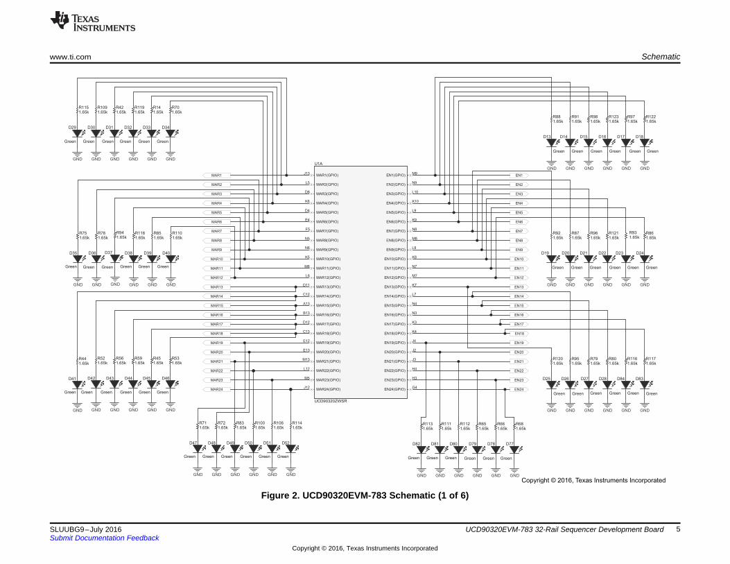
Figure 2. UCD90320EVM-783 Schematic (1 of 6)

DMON5
GND
1.65kR99
Green
D56
GPIO3
GPIO1
GPIO2
GPIO4
DMON4
GND GND GND
GND
1.65kR43
1.65kR58
1.65kR60
1.65kR51
GND
1.65kR55
Green
D57
Green
D12
Green
D11
Green
D9
Green
D10
EN29
EN30
EN31
EN28
EN27
DMON3
EN26
EN25
DMON1
DMON2
GNDGND
GNDGND
1.65kR73
1.65kR74
1.65kR76
1.65kR77
GND
1.65kR67
GND
1.65kR69
GND
1.65kR61
GND
1.65kR62
GND
1.65kR63
GND
1.65kR64
Green
D62
Green
D65
Green
D64
Green
D63
Green
D59
Green
D60
Green
D67
Green
D68
Green
D58
Green
D66
LGPO15
EN32
LGPO9
LGPO13
GND
1.65kR107
GND
1.65kR108
GND
1.65kR101
GND
1.65kR105
Green
D1
Green
D5
Green
D61
Green
D7
DMON6
DMON7
LGPO16
LGPO14
DMON8
GND
1.65kR82
GND
1.65kR84
GND
1.65kR89
GND
1.65kR90
GND
1.65kR81
Green
D8
Green
D6
Green
D53
Green
D55
Green
D54
LGPO1
LGPO4
LGPO7
LGPO6
LGPO8
LGPO2
LGPO3
LGPO5
1.65kR54
GNDGND
GND
GND
GND
GNDGND GND
1.65kR41
1.65kR57
1.65kR50
1.65kR49
1.65kR48
1.65kR47
1.65kR46
Green
D72
Green
D74
Green
D69
Green
D71
Green
D70
Green
D73
Green
D76
Green
D75
LGPO12
LGPO11
LGPO10
GND
1.65kR102
GND
1.65kR103
GND
1.65kR104
Green
D2
Green
D3
Green
D4
SYNC_CLOCK
LGPO13(GPIO)L4
DMON6(GPIO)N12
DMON7(GPIO)N11
DMON8(GPIO)M11
LGPO14(GPIO)N1
GPIO1B11
GPIO2B12
GPIO3C11
GPIO4A12
LGPO15(GPIO)M4
LGPO16(GPIO)N2
DMON1(GPIO)F4
DMON2(GPIO)F3
DMON3(GPIO)G3
DMON4(GPIO)D10
DMON5(GPIO)L11
SYNC_CLKK2
LGPO1(GPIO)C9
LGPO10(GPIO)M1
LGPO11(GPIO)M2
LGPO12(GPIO)M3
LGPO2(GPIO)B9
LGPO3(GPIO)A9
LGPO4(GPIO)C8
LGPO5(GPIO)D5
LGPO6(GPIO)C5
LGPO7(GPIO)C6
LGPO8(GPIO)C4
LGPO9(GPIO)L3
EN25(GPIO)F13
EN26(GPIO)F12
EN27(GPIO)G11
EN28(GPIO)H10
EN29(GPIO)H13
EN30(GPIO)H12
EN31(GPIO)H11
EN32(GPIO)L13
U1B
UCD90320ZWSR
Copyright © 2016, Texas Instruments Incorporated
Schematic www.ti.com
6 SLUUBG9–July 2016Submit Documentation Feedback
Copyright © 2016, Texas Instruments Incorporated
UCD90320EVM-783 32-Rail Sequencer Development Board
Figure 3. UCD90320EVM-783 Schematic (2 of 6)
VDD
GND
1.0k
R11PMBUS_ADDR0
PMBUS_ADDR1
PMBUS_ADDR2
1
2
3
J21
VDD
GND
1.0k
R121
2
3
J22
VDD
GND
1.0k
R131
2
3
J23
AMON20
AMON19
AMON17
AMON18
AMON4
AMON3
200R33
200R34
200R18
200R17
200R32
200R31
AMON2
AMON1200R15
AMON15
AMON16
AMON5
AMON7
AMON9
AMON11
AMON21
AMON23
200R23
200R25
200R35
200R37
200R29
200R30
200R19
200R21
AMON8
AMON6
AMON10
AMON12
AMON22
AMON24
200R20
200R22
200R24
200R26
200R36
200R38
AMON14
AMON13200R27
200R28
TP2 TP3 TP4 TP5 TP6 TP1
GND
0.01µFC1
GND
1µFC7 1µF
C8
VDD
GND
10µFC15
0.1µFC2
+3V0_VREF
JTAG_TCK
JTAG_TMS
JTAG_TDO
JTAG_TDI
PMB_CTRL
PMB_SCL
TP12
TP11
PMB_CTRL
PMB_SCL
PMB_SDA
TP10
PMB_ALERT
TP13
PMB_ALERT
PMBUS_ADDR2
PMBUS_ADDR1
PMBUS_ADDR0
PMB_SDA
GND
VDD
RESET
GND
4.7kR1
TP14
1 2
34
S1RESET
VDD VDDA
1µF
C4
GND
0.1µF
C9
0.01µF
C3
0.1
R3
0.1µFC22
1µFC25
1µFC26
0.1µFC24
0.1µFC21
0.01µFC20
0.01µFC19
GND
1.0
R4+3V3
0.1µFC10
1µFC12
1µFC13
1µFC14
0.1µFC11
GND
GND
GND
VDD
1000pFC5
0.1µFC23
VIN2
TEMP3
GND4
TRIM/NR5
VOUT6
U2A
REF5030AIDGKT
DNC1
NC7
DNC8
U2B
REF5030AIDGKT
200R16
AMON1E2
AMON10A5
AMON11B6
AMON12A6
AMON13C1
AMON14C2
AMON15B1
AMON16B2
AMON17G2
AMON18G1
AMON19H1
AMON2E1
AMON20H2
AMON21B7
AMON22A7
AMON23B8
AMON24A8
AMON3F2
AMON4F1
AMON5B3
AMON6A3
AMON7B4
AMON8A4
AMON9B5
VREFA-D1
VREFA+D2
U1C
UCD90320ZWSR
JTAG_TCKC10
JTAG_TDIB10
JTAG_TDOA11
JTAG_TMSA10
UNUSED-NCA2
UNUSED-DVSSG12
UNUSED-NCG13
UNUSED-DVSSK11
UNUSED-V33DK12
UNUSED-DVSSM10
UNUSED-NCM12
UNUSED-NCN10
UNUSED-DVSSN13
PMB_ALERTF11
PMB_ADDR0L2
PMB_ADDR1L1
PMB_ADDR2K1
PMB_CLKE10
PMB_CTRLE11
PMB_DATAD13
U1D
UCD90320ZWSR
AVSSC3
AVSSE3
BPCAPD6
BPCAPJ1
BPCAPJ6
BPCAPK13
DVSSA1
DVSSC7
DVSSD9
DVSSE5
DVSSF9
DVSSH5
DVSSH9
DVSSJ5
DVSSJ8
DVSSJ11
V33AD3
V33DD7
V33DE6
V33DE8
V33DE9
V33DF10
V33DJ7
V33DJ9
V33DJ10
RESETG10
DVSSE7
DVSSF6
DVSSF7
DVSSF8
DVSSG5
DVSSG6
DVSSG7
DVSSG8
DVSSG9
DVSSH6
DVSSH7
DVSSH8
U1E
UCD90320ZWSR
SH-J1
SH-J2
SH-J3
Copyright © 2016, Texas Instruments Incorporated
www.ti.com Schematic
7SLUUBG9–July 2016Submit Documentation Feedback
Copyright © 2016, Texas Instruments Incorporated
UCD90320EVM-783 32-Rail Sequencer Development Board
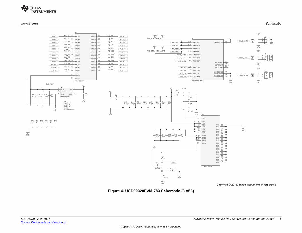
Figure 4. UCD90320EVM-783 Schematic (3 of 6)

LGPO8
LGPO9
LGPO10
LGPO11
GPIO4
LGPO13
LGPO14
LGPO15
LGPO12
LGPO1
LGPO2
LGPO3
LGPO4
LGPO5
LGPO6
LGPO7
MAR24
MAR1
MAR2
MAR3
MAR4
MAR5
MAR6
MAR7
MAR8
MAR9
MAR10
MAR11
MAR12
MAR13
MAR14
MAR15
MAR16
MAR17
MAR18
MAR19
MAR20
MAR21
MAR22
MAR23
EN24
EN1
EN2
EN3
EN4
EN5
EN6
EN7
EN8
EN9
EN10
EN11
EN12
EN13
EN14
EN15
EN16
EN17
EN18
EN19
EN20
EN21
EN22
EN23
PMBUS_ADDR0
PMBUS_ADDR1
PMBUS_ADDR2
SYNC_CLOCK
EN32
GPIO1
GPIO2
GPIO3
DMON8
EN25
EN26
EN27
EN28
EN29
EN30
EN31
DMON2
DMON3
DMON4
DMON5
DMON6
DMON7
AMON24
AMON1
AMON2
AMON3
AMON4
AMON5
AMON6
AMON7
AMON8
AMON9
AMON10
AMON11
AMON12
AMON13
AMON14
AMON15
AMON16
AMON17
AMON18
AMON19
AMON20
AMON21
AMON22
AMON23
PMB_ALERT
PMB_SDAPMB_SCL
PMB_CTRL
+3V3_USB
JTAG_TCK
JTAG_TDO
JTAG_TDI
JTAG_TMS
0.01µFC17
GND
+3V3
1µFC16
GND
Green
D86
330
R136
GND
J26
0R9
GND
10µFC27
4.7k
R39
4.7k
R40
LGPO16
DMON1
PMB_CTRLQ2
GND
Green
D85
330R133
30.1k
R135
Red
D87
NC1
A2
GND3
Y4
VCC5
U5
SN74LVC1G04DBVR
Q1
GND
330R2
30.1k
R134
PMB_ALERT
GND
4.5-5.5V
J24
GND
GND
5
4
1
2
3
6
7
8
J1
5
4
1
2
3
6
7
8
J2
5
4
1
2
3
6
7
8
J3
5
4
1
2
3
6
7
8
J4
5
4
1
2
3
6
7
8
J5
5
4
1
2
3
6
7
8
J6
5
4
1
2
3
6
7
8
J7
5
4
1
2
3
6
7
8
J8
5
4
1
2
3
6
7
8
J9
5
4
1
2
3
6
7
8
J10
5
4
1
2
3
6
7
8
J11
5
4
1
2
3
6
7
8
J14
5
4
1
2
3
6
7
8
J15
5
4
1
2
3
6
7
8
J16
1 2
3 4
5 6
7 8
9 10
11 12
13 14
J131 2
3 4
5 6
7 8
9 10
J12 Remove pin location 6
4.7k
R10
OUT1
NR3
4
GND
EN5
IN8
9
U4A
TPS73633DRBR
NC2
NC6
NC7
U4B
TPS73633DRBR
5V VIN
+3V3+3V3
+3V3
1
2
3
4
5
6
7
8 9
10
11
12
13
14
15
16
680
R5
1
2
3
4
5
6
7
8 9
10
11
12
13
14
15
16
680
R7
1
2
3
4
5
6
7
8 9
10
11
12
13
14
15
16
680
R8
1
2
3
4
5
6
7
8 9
10
11
12
13
14
15
16
680
R6
5
4
1
2
3
6
7
8
J17
5
4
1
2
3
6
7
8
J18
5
4
1
2
3
6
7
8
J19
5
4
1
2
3
6
7
8
J20
+3V3
+3V3
GND
GND
TP8
TP9
30
R161
30
R162
30
R163
30
R164
30
R165
30
R166
30
R167
30
R160
30
R169
30
R170
30
R171
30
R182
30
R183
30
R172
30
R173
30
R168
30
R175
30
R176
30
R177
30
R178
30
R179
30
R180
30
R181
30
R174
SH-J4
Copyright © 2016, Texas Instruments Incorporated
Schematic www.ti.com
8 SLUUBG9–July 2016Submit Documentation Feedback
Copyright © 2016, Texas Instruments Incorporated
UCD90320EVM-783 32-Rail Sequencer Development Board
Figure 5. UCD90320EVM-783 Schematic (4 of 6)
AGND5
BOOT13
COMP7
EN15
GND3
PH10
PAD17
PWRGD14
RT/CLK8
SS/TR9
VIN1
VSENSE6
GND4
PH11
PH12
VIN2
VIN16
U3
TPS54678RTER
0
R124
0.1µF
C28
22µFC34
22µFC35
22µFC36
22µFC37
0.1µFC32
82.5kR137
20.0kR128
10kR129
2700pFC38
DNPC6DNP
GND
500kHz
POL1_EN
GND
40.2R125
20.0kR127
22µFC29
22µFC30
22µFC31
1uH 12A
L1
0.01µFC18
J25
5V VIN
4
1
2
3
J27
+3V3
20.0kR126
POL1_PG
POL1_EN
POL1_PG
POL1_Vout
POL1_Vout
POL1_Margin
POL1_Margin10kR132
508kHz PWM
6800pFC33
AGND5
BOOT13
COMP7
EN15
GND3
PH10
PAD17
PWRGD14
RT/CLK8
SS/TR9
VIN1
VSENSE6
GND4
PH11
PH12
VIN2
VIN16
U6
TPS54678RTER
0
R138
0.1µF
C39
22µFC44
22µFC45
22µFC46
22µFC47
0.1µFC43
82.5kR147
20.0kR143
10kR144
2700pFC50
DNPC48DNP
GND
500kHz
POL2_EN
GND
40.2R140
20.0kR141
22µFC40
22µFC41
22µFC42
1uH 12A
L2
0.01µFC49
J28
5V VIN
4
1
2
3
J29
+3V3
20.0kR139
POL2_PG
POL2_EN
POL2_PG
POL2_Vout
POL2_Vout
POL2_Margin
POL2_Margin10kR142
508kHz PWM
6800pFC51
1.00k
R131
1.00k
R146
196k
R130
196k
R145
SH-J5
SH-J6
Copyright © 2016, Texas Instruments Incorporated
www.ti.com Schematic
9SLUUBG9–July 2016Submit Documentation Feedback
Copyright © 2016, Texas Instruments Incorporated
UCD90320EVM-783 32-Rail Sequencer Development Board
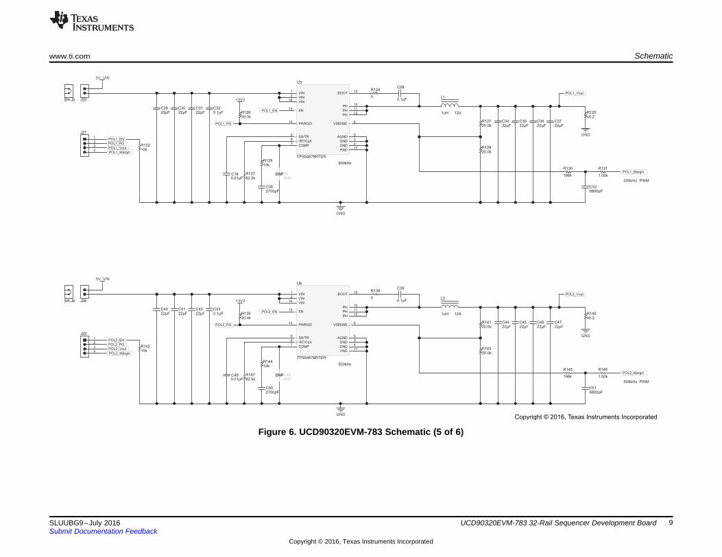
Figure 6. UCD90320EVM-783 Schematic (5 of 6)

GND
GND
GND
0.01µFC57
0.01µFC56
GND
47µFC53
10µFC54
10µFC55
GND
47µFC52
OUT1
SNS2
FB3
PG4
50 mV5
100 mV6
200 mV7
GND8
400 mV9
800 mV10
1.6 V11
BIAS12
NR/SS13
EN14
IN15
IN16
IN17
GND18
OUT19
OUT20
PAD21
U7
TPS7A8400RGRR
J30
5V VIN
4
1
2
3
J31
LDO1_PG
LDO1_EN
LDO1_Vout
LDO1_Margin
10kR149
516kHz PWM
1.00k
R152
20.0kR148
+3V3
LDO1_PG
LDO1_Margin
LDO1_Vout
LDO1_EN
12.1kR150
24.3kR153
120k
R151
0.033µFC58
GND
GND
GND
0.01µFC64
0.01µFC63
GND
47µFC60
10µFC61
10µFC62
GND
47µFC59
OUT1
SNS2
FB3
PG4
50 mV5
100 mV6
200 mV7
GND8
400 mV9
800 mV10
1.6 V11
BIAS12
NR/SS13
EN14
IN15
IN16
IN17
GND18
OUT19
OUT20
PAD21
U8
TPS7A8400RGRR
J32
5V VIN
4
1
2
3
J33
LDO2_PG
LDO2_EN
LDO2_Vout
LDO2_Margin
10kR155
516kHz PWM
1.00k
R158
20.0kR154
+3V3
LDO2_PG
LDO2_Margin
LDO2_Vout
LDO2_EN
12.1kR156
24.3kR159
120k
R157
0.033µFC65
SH-J7
SH-J8
Copyright © 2016, Texas Instruments Incorporated
Schematic www.ti.com
10 SLUUBG9–July 2016Submit Documentation Feedback
Copyright © 2016, Texas Instruments Incorporated
UCD90320EVM-783 32-Rail Sequencer Development Board
Figure 7. UCD90320EVM-783 Schematic (6 of 6)
www.ti.com Test Setup
11SLUUBG9–July 2016Submit Documentation Feedback
Copyright © 2016, Texas Instruments Incorporated
UCD90320EVM-783 32-Rail Sequencer Development Board
5 Test Setup
5.1 Test EquipmentThe following test equipment is recommended when using the EVM:
Voltage Source: One 5-volt power supply with at least 0.5A sourcing capability.Multimeters: One volt-meterOutput Load: NoneOscilloscope: OptionalFan: NoneRecommended Wire Gauge: AWG24 or thickerRecommended PC platform: Windows 7 64-bit with 8GB RAMUSB Interface Adapter EVM (USB-to-GPIO): HPA172The latest version Fusion Digital Power Designer software can be downloaded at the followinglink to the Texas Instruments website:http://focus.ti.com/docs/toolsw/folders/print/fusion_digital_power_designer.html
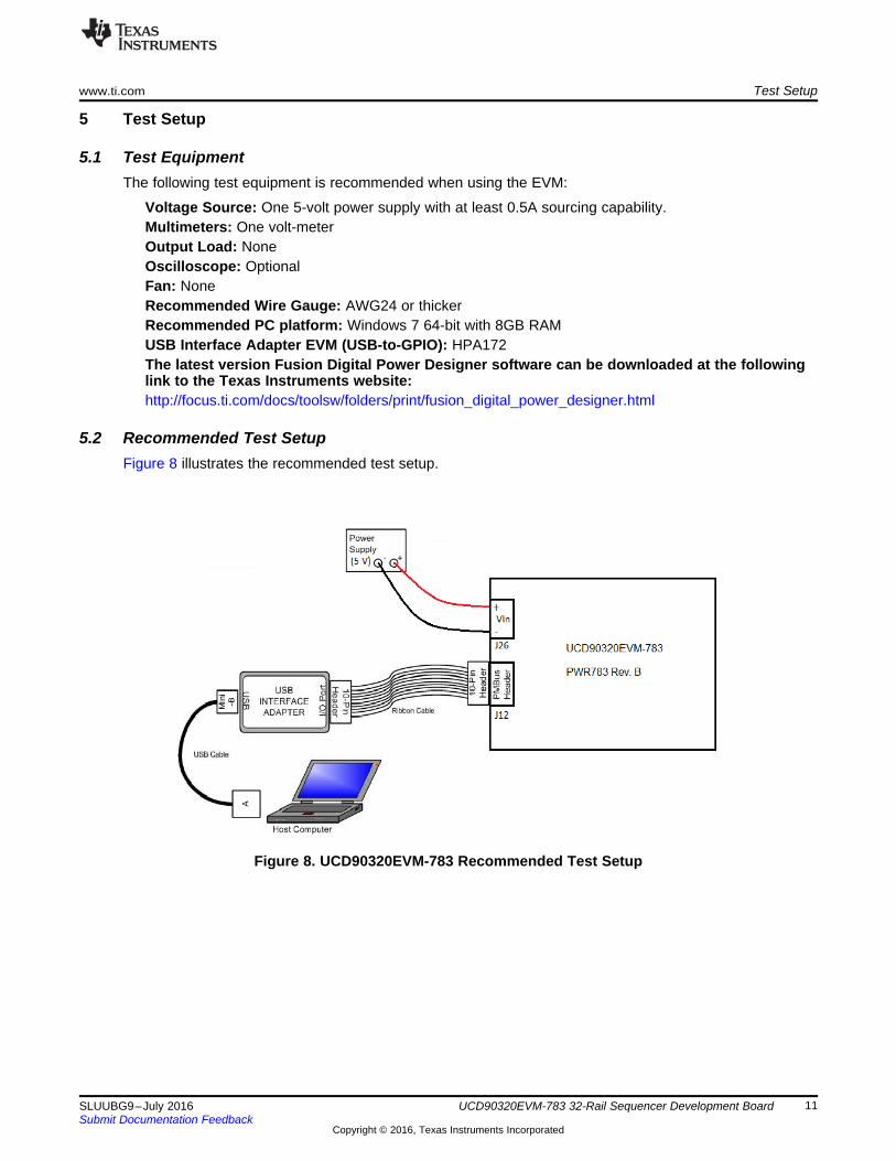
5.2 Recommended Test SetupFigure 8 illustrates the recommended test setup.
Figure 8. UCD90320EVM-783 Recommended Test Setup

Test Setup www.ti.com
12 SLUUBG9–July 2016Submit Documentation Feedback
Copyright © 2016, Texas Instruments Incorporated
UCD90320EVM-783 32-Rail Sequencer Development Board
5.3 List of Connectors and FunctionsTable 2 lists the connectors and their functions.
Table 2. Connector DefinitionsConnectors Pins Name Description
J1 1 MAR01 Margin PWM output or GPIO
2 MAR02 Margin PWM output or GPIO
3 MAR03 Margin PWM output or GPIO
4 MAR04 Margin PWM output or GPIO
5 MAR05 Margin PWM output or GPIO
6 MAR06 Margin PWM output or GPIO
7 MAR07 Margin PWM output or GPIO
8 MAR08 Margin PWM output or GPIO
J2 1 MAR09 Margin PWM output or GPIO
2 MAR10 Margin PWM output or GPIO
3 MAR11 Margin PWM output or GPIO
4 MAR12 Margin PWM output or GPIO
5 MAR13 Margin PWM output or GPIO
6 MAR14 Margin PWM output or GPIO
7 MAR15 Margin PWM output or GPIO
8 MAR16 Margin PWM output or GPIO
J3 1 MAR17 Margin PWM output or GPIO
2 MAR18 Margin PWM output or GPIO
3 MAR19 Margin PWM output or GPIO
4 MAR20 Margin PWM output or GPIO
5 MAR21 Margin PWM output or GPIO
6 MAR22 Margin PWM output or GPIO
7 MAR23 Margin PWM output or GPIO
8 MAR24 Margin PWM output or GPIO
J4 1 EN1 Rail enable output or GPIO
2 EN2 Rail enable output or GPIO
3 EN3 Rail enable output or GPIO
4 EN4 Rail enable output or GPIO
5 EN5 Rail enable output or GPIO
6 EN6 Rail enable output or GPIO
7 EN7 Rail enable output or GPIO
8 EN8 Rail enable output or GPIO
J5 1 EN9 Rail enable output or GPIO
2 EN10 Rail enable output or GPIO
3 EN11 Rail enable output or GPIO
4 EN12 Rail enable output or GPIO
5 EN13 Rail enable output or GPIO
6 EN14 Rail enable output or GPIO
7 EN15 Rail enable output or GPIO
8 EN16 Rail enable output or GPIO
J6 1 EN17 Rail enable output or GPIO
2 EN18 Rail enable output or GPIO
3 EN19 Rail enable output or GPIO
4 EN20 Rail enable output or GPIO
5 EN21 Rail enable output or GPIO
6 EN22 Rail enable output or GPIO
7 EN23 Rail enable output or GPIO
8 EN24 Rail enable output or GPIO

www.ti.com Test Setup
13SLUUBG9–July 2016Submit Documentation Feedback
Copyright © 2016, Texas Instruments Incorporated
UCD90320EVM-783 32-Rail Sequencer Development Board
Table 2. Connector Definitions (continued)Connectors Pins Name Description
J7 1 LGPO1 Logic GPO output or GPIO
2 LGPO2 Logic GPO output or GPIO
3 LGPO3 Logic GPO output or GPIO
4 LGPO4 Logic GPO output or GPIO
5 LGPO5 Logic GPO output or GPIO
6 LGPO6 Logic GPO output or GPIO
7 LGPO7 Logic GPO output or GPIO
8 LGPO8 Logic GPO output or GPIO
J8 1 LGPO9 Logic GPO output or GPIO
2 LGPO10 Logic GPO output or GPIO
3 LGPO11 Logic GPO output or GPIO
4 LGPO12 Logic GPO output or GPIO
5 LGPO13 Logic GPO output or GPIO
6 LGPO14 Logic GPO output or GPIO
7 LGPO15 Logic GPO output or GPIO
8 LGPO16 Logic GPO output or GPIO
J9 1 PMBUS_ADDR0 PMBus address pin
2 PMBUS_ADDR1 PMBus address pin
3 PMBUS_ADDR2 PMBus address pin
4 SYNC_CLOCK Sync Clock pin
5 GPIO1 General Purpose I/O
6 GPIO2 General Purpose I/O
7 GPIO3 General Purpose I/O
8 GPIO4 General Purpose I/O
J10 1 EN25 Rail enable output or GPIO
2 EN26 Rail enable output or GPIO
3 EN27 Rail enable output or GPIO
4 EN28 Rail enable output or GPIO
5 EN29 Rail enable output or GPIO
6 EN30 Rail enable output or GPIO
7 EN31 Rail enable output or GPIO
8 EN32 Rail enable output or GPIO
J11 1 DMON1 Digital monitor input or GPIO
2 DMON2 Digital monitor input or GPIO
3 DMON3 Digital monitor input or GPIO
4 DMON4 Digital monitor input or GPIO
5 DMON5 Digital monitor input or GPIO
6 DMON6 Digital monitor input or GPIO
7 DMON7 Digital monitor input or GPIO
8 DMON8 Digital monitor input or GPIO
J12 1 No connection
2 No connection
3 No connection
4 No connection
5 +3V3_USB 3.3-V power provided by USB interface adapter EVM
6 GND PMBus GND
7 PMB_CTRL PMBus CONTROL line
8 PMB_ALERT PMBus ALERT# line
9 PMB_SCL PMBus Clock
10 PMB_SDA PMBus Data
J13 1 JTAG_TMS JTAG TMS

Test Setup www.ti.com
14 SLUUBG9–July 2016Submit Documentation Feedback
Copyright © 2016, Texas Instruments Incorporated
UCD90320EVM-783 32-Rail Sequencer Development Board
Table 2. Connector Definitions (continued)Connectors Pins Name Description
2 JTAG nTRST (unused)
3 JTAG_TDI JTAG TDI
4 JTAG TDIS (unused)
5 JTAG VTRef (unused)
6 JTAG KEY
7 JTAG_TDO JTAG TDO
8 GND JTAG GND
9 JTAG RTCK (unused)
10 GND JTAG GND
11 JTAG_TCK JTAG TCK
12 GND JTAG GND
13 JTAG EMU0 (unused)
14 JTAG EMU1 (unused)
J14 1 AMON1 Analog monitor input
2 AMON2 Analog monitor input
3 AMON3 Analog monitor input
4 AMON4 Analog monitor input
5 AMON5 Analog monitor input
6 AMON6 Analog monitor input
7 AMON7 Analog monitor input
8 AMON8 Analog monitor input
J15 1 AMON9 Analog monitor input
2 AMON10 Analog monitor input
3 AMON11 Analog monitor input
4 AMON12 Analog monitor input
5 AMON13 Analog monitor input
6 AMON14 Analog monitor input
7 AMON15 Analog monitor input
8 AMON16 Analog monitor input
J16 1 AMON17 Analog monitor input
2 AMON18 Analog monitor input
3 AMON19 Analog monitor input
4 AMON20 Analog monitor input
5 AMON21 Analog monitor input
6 AMON22 Analog monitor input
7 AMON23 Analog monitor input
8 AMON24 Analog monitor input
J17 1 Pull-up signal (can be used as GPI input)
2 Pull-up signal (can be used as GPI input)
3 Pull-up signal (can be used as GPI input)
4 Pull-up signal (can be used as GPI input)
5 Pull-up signal (can be used as GPI input)
6 Pull-up signal (can be used as GPI input)
7 Pull-up signal (can be used as GPI input)
8 Pull-up signal (can be used as GPI input)
J18 1 Pull-up signal (can be used as GPI input)
2 Pull-up signal (can be used as GPI input)
3 Pull-up signal (can be used as GPI input)
4 Pull-up signal (can be used as GPI input)
5 Pull-up signal (can be used as GPI input)
6 Pull-up signal (can be used as GPI input)

www.ti.com Test Setup
15SLUUBG9–July 2016Submit Documentation Feedback
Copyright © 2016, Texas Instruments Incorporated
UCD90320EVM-783 32-Rail Sequencer Development Board
Table 2. Connector Definitions (continued)Connectors Pins Name Description
7 Pull-up signal (can be used as GPI input)
8 Pull-up signal (can be used as GPI input)
J19 1 Pull-down signal (can be used as GPI input)
2 Pull-down signal (can be used as GPI input)
3 Pull-down signal (can be used as GPI input)
4 Pull-down signal (can be used as GPI input)
5 Pull-down signal (can be used as GPI input)
6 Pull-down signal (can be used as GPI input)
7 Pull-down signal (can be used as GPI input)
8 Pull-down signal (can be used as GPI input)
J20 1 Pull-down signal (can be used as GPI input)
2 Pull-down signal (can be used as GPI input)
3 Pull-down signal (can be used as GPI input)
4 Pull-down signal (can be used as GPI input)
5 Pull-down signal (can be used as GPI input)
6 Pull-down signal (can be used as GPI input)
7 Pull-down signal (can be used as GPI input)
8 Pull-down signal (can be used as GPI input)
J21 1 VDD VDD (connect to pin 2 to pullup)
2 Floating pin connected to PMBUS_ADDR0 through 1-kΩ resistor
3 GND GND (connect to pin 2 to pulldown)
J22 1 VDD VDD (connect to pin 2 to pullup)
2 Floating pin connected to PMBUS_ADDR1 through 1-kΩ resistor
3 GND GND (connect to pin 2 to pulldown)
J23 1 VDD VDD (connect to pin 2 to pullup)
2 Floating pin connected to PMBUS_ADDR2 through 1-kΩ resistor
3 GND GND (connect to pin 2 to pulldown)
J24 1 +3V3_USB 3.3-V power provided by USB interface adapter EVM
2 +3V3 3.3-V rail to power VDD. Install a shut jumper to this connector to supply VDD from USBinterface adapter.
J25 1 5V Connected to 5-V VIN
2 VIN for POL. Connect to pin 1 to supply 5-V VIN to POL.
J26 1 5V_VIN 5-V input power positive terminal
2 GND 5-V input power negative terminal
J27 1 POL1_EN Connect this pin to an EN pin to test enable function
2 POL1_PG Connect this pin to a DMON pin to test digital monitor function
3 POL1_VOUT Connect this pin to an AMON pin to test analog monitor function
4 POL1_MAR Connect this pin to a MAR pin to test margining function
J28 1 5V Connected to 5-V VIN
2 VIN for POL. Connect to pin 1 to supply 5-V VIN to POL.
J29 1 POL2_EN Connect this pin to an EN pin to test enable function
2 POL2_PG Connect this pin to a DMON pin to test digital monitor function
3 POL2_VOUT Connect this pin to an AMON pin to test analog monitor function
4 POL2_MAR Connect this pin to a MAR pin to test margining function
J30 1 5V Connected to 5-V VIN
2 VIN for POL. Connect to pin 1 to supply 5-V VIN to POL.
J31 1 POL3_EN Connect this pin to an EN pin to test enable function
2 POL3_PG Connect this pin to a DMON pin to test digital monitor function
3 POL3_VOUT Connect this pin to an AMON pin to test analog monitor function
4 POL3_MAR Connect this pin to a MAR pin to test margining function
J32 1 5V Connected to 5-V VIN
2 VIN for POL. Connect to pin 1 to supply 5-V VIN to POL.
Test Setup www.ti.com
16 SLUUBG9–July 2016Submit Documentation Feedback
Copyright © 2016, Texas Instruments Incorporated
UCD90320EVM-783 32-Rail Sequencer Development Board
Table 2. Connector Definitions (continued)Connectors Pins Name Description
J33 1 POL4_EN Connect this pin to an EN pin to test enable function
2 POL4_PG Connect this pin to a DMON pin to test digital monitor function
3 POL4_VOUT Connect this pin to an AMON pin to test analog monitor function
4 POL4_MAR Connect this pin to a MAR pin to test margining function

www.ti.com Test Setup
17SLUUBG9–July 2016Submit Documentation Feedback
Copyright © 2016, Texas Instruments Incorporated
UCD90320EVM-783 32-Rail Sequencer Development Board
5.4 List of Test PointsTable 3 lists and describes the test points.
Table 3. Test Points Functions
TestPoints
Name Description
TP1 GND GroundTP2 GND GroundTP3 GND GroundTP4 GND GroundTP5 GND GroundTP6 GND GroundTP8 5V_VIN 5-V input power positive terminalTP9 GND GroundTP10 PMB_SDA PMBus DataTP11 PMB_CTRL PMBus CONTROL lineTP12 PMB_SCL PMBus ClockTP13 PMB_ALERT PMBus ALERT# lineTP14 RESET UCD90320 reset pin signal
6 Software SetupAccessing the configuration of the UCD90320EVM-783, control and monitoring capabilities with the FusionDigital Power Designer software tool requires a one-time software setup per host system.
6.1 Fusion Digital Power Designer Software (Fusion GUI) InstallationPlace the Fusion Digital Power Designer Software (Fusion GUI) installer executable file in a knownlocation on the host computer to be used for EVM configuration and test.
Double click the TI-Fusion-Digital-Power-Designer-2.0.xxx.exe file and proceed through the installation byaccepting the installer prompts and the license agreement. Use the Fusion GUI installer’s suggesteddefault installation locations to complete the install.
When the Fusion GUI installation reaches the finished window, uncheck the Launch application checkbox and close the window.
7 Test ProcedureThe UCD90320EVM-783_Default_Configuration.xml file is found on the TI website and is provided toallow the user to return the EVM to its originally-configured state. Open the Fusion GUI while the poweredEVM is connected to the computer with the USB interface adapter. In the Fusion GUI interface, select File→ Import Project and the Project Open Wizard window opens.
7.1 Voltage Monitoring ExampleConnect the EVM as shown in Figure 8. Connect 5-V VIN to J26. Open the Fusion Digital Power DesignerGUI by navigating to the Start → Texas Instruments Fusion Digital Power Designer → Fusion DigitalPower Designer (not the offline version which would have monitoring disabled).
All AMON and DMON pins are assigned to corresponding rails in the default configuration file. Connect awire jumper from POL1_VOUT to the AMON1 pin. Connect a wire jumper from POL1_EN to a pull-up pinin J18. The output voltage of POL1 will be displayed as Vout #1 voltage in the Fusion GUI → Monitorpage. Note that floating AMON pins give non-zero readings, which is an expected behavior.

Test Procedure www.ti.com
18 SLUUBG9–July 2016Submit Documentation Feedback
Copyright © 2016, Texas Instruments Incorporated
UCD90320EVM-783 32-Rail Sequencer Development Board
7.2 Rail Enable ExampleIn the default configuration file, all EN pins are assigned to corresponding rails, and all rails are controlledby the CONTROL pin. The pin assignments are shown in the Fusion GUI → Configure page →Hardware Configuration tab. The CONTROL pin status can be controlled in the Fusion GUI → Monitorpage. Turn on the CONTROL Line in the Monitor page. Observe that all LEDs attached to EN pins are lit.
7.3 Fault Log Example (Including Blackbox Log)In the Status page, click the Clear Faults button, the Clear Logged Faults button, and the ClearBlackbox Log button to clear all previous faults. In Configure page → Global Configuration tab →Set/Sync Device Clock window, click Set Device Clock to Local PC Time button to update device runtime clock.
With the CONTROL line being asserted, disconnect the jumper wire from the POL1_EN pin, whichdisables the POL1 output. Since the CONTROL line is asserted, and Rail #1 is previously in Power Goodcondition, the unexpected POL1 output drop will cause a VOUT UV fault. In the Status page → StatusRegisters tab, observe that the VOUT UV Fault of Rail #1 is raised. In the Logged Faults tab, observe thatthe VOUT UV Fault of Rail #1 is also raised. In the Blackbox Info tab, click the Refresh Blackbox Logbutton. Observe that all the fault information and status of all the GPI, GPO, and rails when the faultoccurred were recorded in the Blackbox Log.
7.4 Command GPO ExampleIn the default configuration file, the GPIO3-4 pins are configured as command GPO. In the Configurepage → Hardware Configuration tab, change the Command GPO states and then click the Write toHardware button. Observe the LED of the corresponding GPIO pin changes state.
7.5 GPI and Logic GPO ExampleIn the default configuration file, the GPIO1 pin is configured as GPI pin with GPI fault enabled. Each of the16 LGPO pins is configured to follow the GPI input with 960-ms time delay. The pin assignments areshown in Configure page → Hardware Configuration tab.
Connect a jumper wire from a pull-up pin in J17 or J18 to the GPI pin. Observe that the LEDs of the 16LGPO pins are lit after 960 ms. Also observe that the corresponding GPI Fault is logged in the Statuspage. Then disconnect the logic input signal from the GPI pin. Observe that the LEDs of the LGPO pinsare out after 960 ms.
7.6 Margin ExampleIn the default configuration file, all 24 analog rails are configured with the margining function. The pinassignments are shown in Configure page → Hardware Configuration tab. Connect POL1 outputvoltage (J27-POL1_VOUT) to AMON1 pin using a jumper wire. Then connect the margin input of POL1(J27-POL1_MAR) to the MAR1 pin. Also, connect the enable pin of POL1 (J27-POL1_EN) to EN1.
In Fusion GUI → Monitor page, turn on the CONTROL line. Observe that the EN1 pin’s LED is lit, andthe on-board POL is enabled. The POL’s output voltage is monitored in the Monitor page, which should beat 1.2 V. In Fusion GUI → Monitor page, click to change margin status to Low. Observe that the POLoutput voltage is regulated at Margin Low level defined in Configure page → Vout Config tab. Then clickto change margin status to High. Observe that the POL output voltage is regulated at Margin High level.
7.7 Cascading Example
7.7.1 Sync ClockSync Clock can synchronize multiple UCD90320 devices such that they respond to the same GPI eventsynchronously, and the same GPI event has the same time stamp in all synchronized UCD90320 devices.The Sync Clock I/O pin is located in J9. Implementing the Sync Clock feature requires two or moreUCD90320EVM-783 boards.

www.ti.com Test Procedure
19SLUUBG9–July 2016Submit Documentation Feedback
Copyright © 2016, Texas Instruments Incorporated
UCD90320EVM-783 32-Rail Sequencer Development Board
In Fusion GUI → Configure page → Global Configuration tab → Misc Config, configure one EVMboard as Sync Clock master, and all other boards as slaves. Connect the multiple EVM boards to thesame ground. Connect all Sync Clock pins to the same node. Observe that the synchronized UCD90320devices respond to the same GPI event synchronously.
When the Sync Clock pin is not used, configure the UCD90320 device as Sync Clock master.
7.7.2 Fault PinMultiple UCD90320 devices can be acknowledged of the same rail fault and react accordingly, even if therail is monitored by only one UCD90320 device. This is achieved with the Fault Pin feature.
In each UCD90320 device, up to 4 GPI pins can be configured as Fault Pins. Each Fault Pin is connectedto a Fault Bus. Each Fault Bus should be pulled up to 3.3 V by a 10-kΩ resistor. When there is no fault ona Fault Bus, the Fault Pins are GPI pins and listen to the Fault Bus. When a rail fault is detected by aUCD90320 device, the corresponding Fault Pin is turned into active driven low state, pulling down theFault Bus and informing all other UCD90320 devices of the corresponding fault.
In the default configuration file, the GPIO2 pin is configured as a Fault Pin. Continuing the previousexample, where CONTROL line is asserted, POL1_EN is connected to EN1, and POL1_VOUT isconnected to AMON1. Connect GPIO2 (Fault Pin) to a pull-up pin in J17 or J18. Then, disconnect thePOL1_VOUT pin from AMON1, observe that the LED of GPIO2 is out due to Rail #1 VOUT UV fault. TheFault Pin configuration is in Fusion GUI → Configure page → Global Configuration tab → Fault PinConfig. Only the faults on selected rails (pages) will trigger the Fault Pin to pulldown.
Reconnect POL1_VOUT to AMON1 so that the Fault Pin is no longer held low by the UCD90320 device.Next, disconnect GPIO2 from the pull-up signal. This simulates the condition that the Fault Bus is pulleddown by another UCD90320 device. Observe that a GPI2 fault is logged in Fusion GUI → Status page→ Logged Faults tab → Logged Faults Detail. This GPI fault can be configured to trigger rail shutdown. The fault response of each rail to GPI faults can be configured in the Fusion GUI → Configurepage → Rail Config tab → GPI Fault Responses window.
The Fault Pin feature and the Sync Clock feature can work together to achieve better synchronized faultresponse performance.
EVM Assembly Drawing and PCB Layout www.ti.com
20 SLUUBG9–July 2016Submit Documentation Feedback
Copyright © 2016, Texas Instruments Incorporated
UCD90320EVM-783 32-Rail Sequencer Development Board
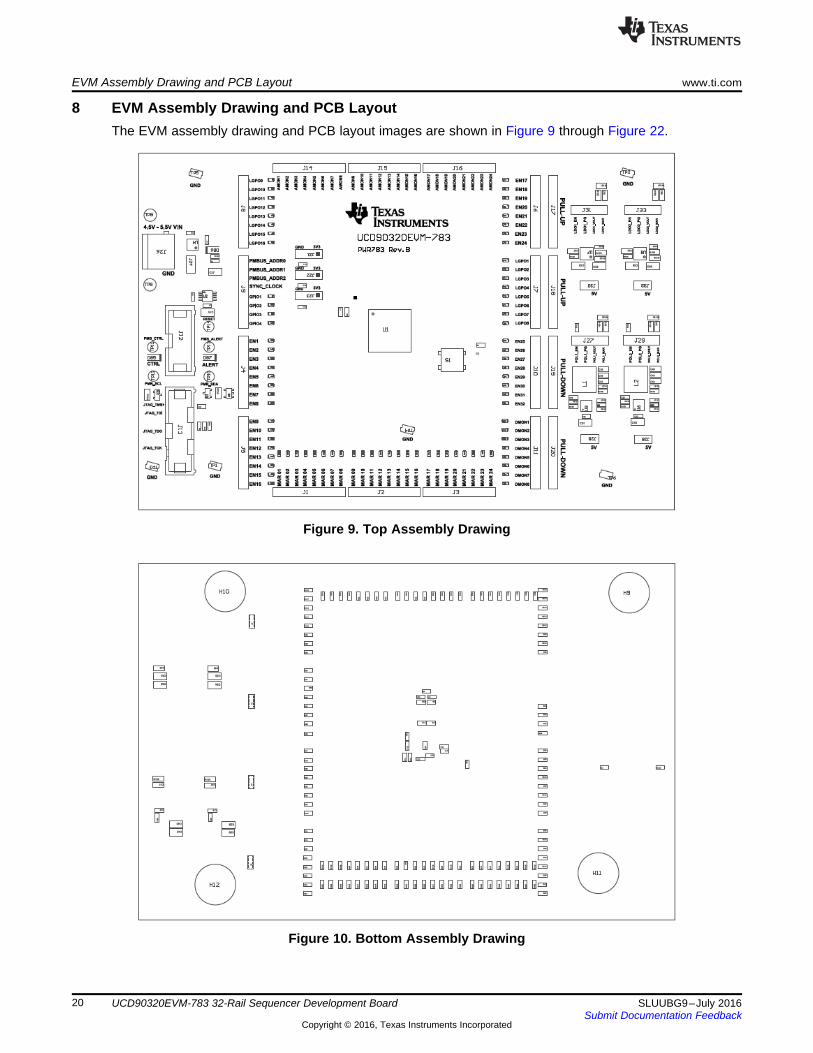
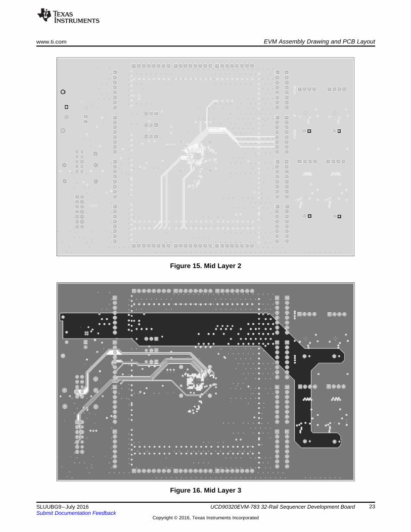
8 EVM Assembly Drawing and PCB LayoutThe EVM assembly drawing and PCB layout images are shown in Figure 9 through Figure 22.
Figure 9. Top Assembly Drawing
Figure 10. Bottom Assembly Drawing

www.ti.com EVM Assembly Drawing and PCB Layout
21SLUUBG9–July 2016Submit Documentation Feedback
Copyright © 2016, Texas Instruments Incorporated
UCD90320EVM-783 32-Rail Sequencer Development Board
Figure 11. Top Overlay
Figure 12. Top Solder Mask

EVM Assembly Drawing and PCB Layout www.ti.com
22 SLUUBG9–July 2016Submit Documentation Feedback
Copyright © 2016, Texas Instruments Incorporated
UCD90320EVM-783 32-Rail Sequencer Development Board
Figure 13. Top Layer
Figure 14. Mid Layer 1
www.ti.com EVM Assembly Drawing and PCB Layout
23SLUUBG9–July 2016Submit Documentation Feedback
Copyright © 2016, Texas Instruments Incorporated
UCD90320EVM-783 32-Rail Sequencer Development Board
Figure 15. Mid Layer 2
Figure 16. Mid Layer 3

EVM Assembly Drawing and PCB Layout www.ti.com
24 SLUUBG9–July 2016Submit Documentation Feedback
Copyright © 2016, Texas Instruments Incorporated
UCD90320EVM-783 32-Rail Sequencer Development Board
Figure 17. Mid Layer 4
Figure 18. Bottom Layer

www.ti.com EVM Assembly Drawing and PCB Layout
25SLUUBG9–July 2016Submit Documentation Feedback
Copyright © 2016, Texas Instruments Incorporated
UCD90320EVM-783 32-Rail Sequencer Development Board
Figure 19. Bottom Solder Mask
Figure 20. Bottom Overlay
EVM Assembly Drawing and PCB Layout www.ti.com
26 SLUUBG9–July 2016Submit Documentation Feedback
Copyright © 2016, Texas Instruments Incorporated
UCD90320EVM-783 32-Rail Sequencer Development Board
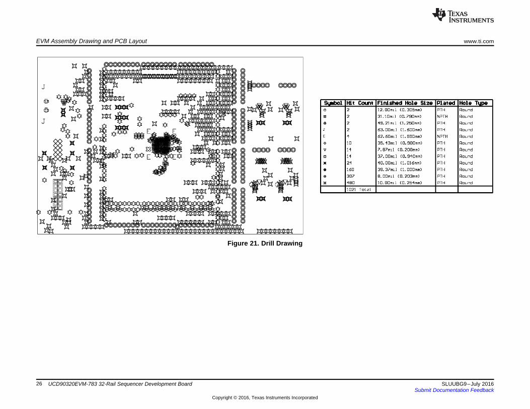
Figure 21. Drill Drawing

www.ti.com EVM Assembly Drawing and PCB Layout
27SLUUBG9–July 2016Submit Documentation Feedback
Copyright © 2016, Texas Instruments Incorporated
UCD90320EVM-783 32-Rail Sequencer Development Board
Figure 22. Board Dimensions

Bill of Material www.ti.com
28 SLUUBG9–July 2016Submit Documentation Feedback
Copyright © 2016, Texas Instruments Incorporated
UCD90320EVM-783 32-Rail Sequencer Development Board
9 Bill of MaterialTable 4 lists the EVM BOM.
Table 4. UCD90320EVM-783 BOMDesignator Qty Value Description Package Reference Part Number Manufacturer Alternate Part Number Alternate
Manufacturer
C1, C3, C18, C19, C20, C49 6 0.01uF CAP, CERM, 0.01 µF, 16 V, +/- 10%, X7R, 0402 0402 C1005X7R1C103K TDK
C2, C9, C10, C11, C21, C22,C23, C24
8 0.1uF CAP, CERM, 0.1 µF, 6.3 V, +/- 10%, X5R, 0402 0402 C1005X5R0J104K TDK
C4, C7, C8, C12, C13, C14,C16, C25, C26
9 1uF CAP, CERM, 1 µF, 25 V, +/- 10%, X5R, 0603 0603 C1608X5R1E105K080AC TDK
C5 1 1000pF CAP, CERM, 1000pF, 50V, +/-5%, X7R, 0603 0603 C0603C102J5RACTU Kemet - -
C15, C27 2 10uF CAP, CERM, 10 µF, 6.3 V, +/- 10%, X6S, 0805 0805 GRM219C80J106KE39D Murata
C17 1 0.01uF CAP, CERM, 0.01 µF, 50 V, +/- 5%, X7R, 0603 0603 C0603C103J5RACTU Kemet
C28, C32, C39, C43 4 0.1uF CAP, CERM, 0.1 µF, 16 V, +/- 10%, X5R, 0402 0402 GRM155R61C104KA88D Murata
C29, C30, C31, C40, C41, C42 6 22uF CAP, CERM, 22 µF, 6.3 V, +/- 20%, X5R, 0805 0805 GRM21BR60J226ME39L Murata
C33, C51 2 6800pF CAP, CERM, 6800 pF, 100 V, +/- 10%, X7R, 0603 0603 06031C682KAT2A AVX
C34, C35, C36, C37, C44,C45, C46, C47
8 22uF CAP, CERM, 22 µF, 6.3 V, +/- 20%, X5R, 0603 0603 C1608X5R0J226M080AC TDK
C38, C50 2 2700pF CAP, CERM, 2700 pF, 50 V, +/- 10%, X7R, 0402 0402 GRM155R71H272KA01D Murata
C52, C53, C59, C60 4 47uF CAP, CERM, 47 µF, 4 V, +/- 20%, X5R, 0805 0805 GRM219R60G476ME44D Murata
C54, C55, C61, C62 4 10uF CAP, CERM, 10 µF, 16 V, +/- 10%, X5R, 0805 0805 GRM21BR61C106KE15L Murata
C56, C57, C63, C64 4 0.01uF CAP, CERM, 0.01 µF, 50 V, +/- 10%, X7R, 0603 0603 GRM188R71H103KA01D Murata
C58, C65 2 0.033uF CAP, CERM, 0.033 µF, 50 V, +/- 5%, X7R, 0603 0603 06035C333JAT2A AVX
D1, D2, D3, D4, D5, D6, D7,D8, D9, D10, D11, D12, D13,D14, D15, D16, D17, D18,D19, D20, D21, D22, D23,D24, D25, D26, D27, D28,D29, D30, D31, D32, D33,D34, D35, D36, D37, D38,D39, D40, D41, D42, D43,D44, D45, D46, D47, D48,D49, D50, D51, D52, D53,D54, D55, D56, D57, D58,D59, D60, D61, D62, D63,D64, D65, D66, D67, D68,D69, D70, D71, D72, D73,D74, D75, D76, D77, D78,D79, D80, D81, D82, D83, D84
84 Green LED, Green, SMD 1.7x0.65x0.8mm LG L29K-G2J1-24-Z OSRAM
D85, D86 2 Green LED, Green, SMD LED_0805 LTST-C171GKT Lite-On
D87 1 Red LED, Red, SMD LED_0805 LTST-C170KRKT Lite-On
H9, H10, H11, H12 4 Bumpon, Hemisphere, 0.44 X 0.20, Clear Transparent Bumpon SJ-5303 (CLEAR) 3M
J1, J2, J3, J4, J5, J6, J7, J8,J9, J10, J11, J14, J15, J16,J17, J18, J19, J20
18 Header, 100mil, 8x1, Tin, TH Header, 8x1, 100mil,TH
PEC08SAAN Sullins ConnectorSolutions
J12 1 Header (shrouded), 100mil, 5x2, Gold, TH TH, 10-Leads, Body8.5x20mm, Pitch2.54mm
XG4C-1031 Omron ElectronicComponents
J13 1 Header (shrouded), 100mil, 7x2, Gold, TH 7x2 Header N2514-6002-RB 3M
www.ti.com Bill of Material
29SLUUBG9–July 2016Submit Documentation Feedback
Copyright © 2016, Texas Instruments Incorporated
UCD90320EVM-783 32-Rail Sequencer Development Board
Table 4. UCD90320EVM-783 BOM (continued)Designator Qty Value Description Package Reference Part Number Manufacturer Alternate Part Number Alternate
Manufacturer
J21, J22, J23 3 Header, 100mil, 3x1, Tin, TH Header, 3 PIN, 100mil,Tin
PEC03SAAN Sullins ConnectorSolutions
J24, J25, J28, J30, J32 5 Header, 100mil, 2x1, Tin, TH Header, 2 PIN, 100mil,Tin
PEC02SAAN Sullins ConnectorSolutions
J26 1 TERMINAL BLOCK 5.08MM VERT 2POS, TH TERM_BLK, 2pos,5.08mm
ED120/2DS On-Shore Technology
J27, J29, J31, J33 4 Header, 100mil, 4x1, Tin, TH Header, 4x1, 100mil,TH
PEC04SAAN Sullins ConnectorSolutions
L1, L2 2 1uH Inductor, Shielded, Ferrite, 1 µH, 12 A, 0.0072 ohm,SMD
Inductor, 7.2x4x6.5mm SRP6540-1R0M Bourns
Q1, Q2 2 60V MOSFET, N-CH, 60 V, 0.17 A, SOT-23 SOT-23 2N7002-7-F Diodes Inc. None
R1, R10, R39, R40 4 4.7k RES, 4.7 k, 5%, 0.1 W, 0603 0603 CRCW06034K70JNEA Vishay-Dale
R2, R133, R136 3 330 RES, 330, 5%, 0.1 W, 0603 0603 CRCW0603330RJNEA Vishay-Dale
R3 1 0.1 RES, 0.1, 1%, 0.1 W, 0603 0603 ERJ-3RSFR10V Panasonic
R4 1 1.0 RES, 1.0, 5%, 0.1 W, 0603 0603 CRCW06031R00JNEA Vishay-Dale
R5, R6, R7, R8 4 680 RES, 680, 5%, 0.0625 W, Resistor Array - 8x1 Resistor Array - 8x1 EXB-2HV681JV Panasonic
R9 1 0 RES, 0, 5%, 0.1 W, 0603 0603 ERJ-3GEY0R00V Panasonic
R11, R12, R13 3 1.0k RES, 1.0 k, 5%, 0.1 W, 0603 0603 RC0603JR-071KL Yageo America
R14, R41, R42, R43, R44,R45, R46, R47, R48, R49,R50, R51, R52, R53, R54,R55, R56, R57, R58, R59,R60, R61, R62, R63, R64,R65, R66, R67, R68, R69,R70, R71, R72, R73, R74,R75, R76, R77, R78, R79,R80, R81, R82, R83, R84,R85, R86, R87, R88, R89,R90, R91, R92, R93, R94,R95, R96, R97, R98, R99,R100, R101, R102, R103,R104, R105, R106, R107,R108, R109, R110, R111,R112, R113, R114, R115,R116, R117, R118, R119,R120, R121, R122, R123
84 1.65k RES, 1.65 k, 1%, 0.1 W, 0603 0603 RC0603FR-071K65L Yageo America
R15, R16, R17, R18, R19,R20, R21, R22, R23, R24,R25, R26, R27, R28, R29,R30, R31, R32, R33, R34,R35, R36, R37, R38
24 200 RES, 200, 0.1%, 0.1 W, 0603 0603 RG1608P-201-B-T5 Susumu Co Ltd
R124, R138 2 0 RES, 0, 5%, 0.063 W, 0402 0402 CRCW04020000Z0ED Vishay-Dale
R125, R140 2 40.2 RES, 40.2, 1%, 0.1 W, 0603 0603 RC0603FR-0740R2L Yageo America
R126, R127, R128, R139,R141, R143, R148, R154
8 20.0k RES, 20.0 k, 1%, 0.063 W, 0402 0402 CRCW040220K0FKED Vishay-Dale
R129, R132, R142, R144,R149, R155
6 10k RES, 10 k, 5%, 0.063 W, 0402 0402 CRCW040210K0JNED Vishay-Dale
R130, R145 2 196k RES, 196 k, 1%, 0.1 W, 0603 0603 CRCW0603196KFKEA Vishay-Dale
R131, R146, R152, R158 4 1.00k RES, 1.00 k, 1%, 0.1 W, 0603 0603 CRCW06031K00FKEA Vishay-Dale
R134, R135 2 30.1k RES, 30.1 k, 1%, 0.1 W, 0603 0603 RC0603FR-0730K1L Yageo America
Bill of Material www.ti.com
30 SLUUBG9–July 2016Submit Documentation Feedback
Copyright © 2016, Texas Instruments Incorporated
UCD90320EVM-783 32-Rail Sequencer Development Board
Table 4. UCD90320EVM-783 BOM (continued)Designator Qty Value Description Package Reference Part Number Manufacturer Alternate Part Number Alternate
Manufacturer
R137, R147 2 82.5k RES, 82.5 k, 1%, 0.063 W, 0402 0402 CRCW040282K5FKED Vishay-Dale
R150, R156 2 12.1k RES, 12.1 k, 1%, 0.1 W, 0603 0603 CRCW060312K1FKEA Vishay-Dale
R151, R157 2 120k RES, 120 k, 5%, 0.1 W, 0603 0603 CRCW0603120KJNEA Vishay-Dale
R153, R159 2 24.3k RES, 24.3 k, 1%, 0.1 W, 0603 0603 CRCW060324K3FKEA Vishay-Dale
R160, R161, R162, R163,R164, R165, R166, R167,R168, R169, R170, R171,R172, R173, R174, R175,R176, R177, R178, R179,R180, R181, R182, R183
24 30 RES, 30, 5%, 0.063 W, 0402 0402 CRCW040230R0JNED Vishay-Dale
S1 1 Switch, Tactile, SPST-NO, 1VA, 32V, SMT Switch, 6.3x5.36x6.6mm, SMT
KT11P2JM34LFS C&K Components
SH-J1, SH-J2, SH-J3, SH-J4,SH-J5, SH-J6, SH-J7, SH-J8
8 1x2 Shunt, 100mil, Gold plated, Black Shunt 969102-0000-DA 3M SNT-100-BK-G Samtec
TP1, TP2, TP3, TP4, TP5, TP6 6 SMT Test Point, Compact, SMT Testpoint_Keystone_Compact
5016 Keystone
TP8 1 Red Test Point, Multipurpose, Red, TH Red MultipurposeTestpoint
5010 Keystone
TP9 1 Black Test Point, Multipurpose, Black, TH Black MultipurposeTestpoint
5011 Keystone
TP10, TP11, TP12, TP13,TP14
5 Yellow Test Point, Miniature, Yellow, TH Yellow MiniatureTestpoint
5004 Keystone
U1 1 32-Rail PMBus Power Sequencer and SystemManager, ZWS0169A
ZWS0169A UCD90320ZWSR Texas Instruments UCD90320ZWST Texas Instruments
U2 1 Low Noise, Very Low Drift, Precision VoltageReference, -40 to 125 degC, 8-pin MSOP (DGK),Green (RoHS & no Sb/Br)
DGK0008A REF5030AIDGKT Texas Instruments Equivalent None
U3, U6 2 2.95 V to 6 V INPUT, 6 A OUTPUT, 2 MHz,SYNCHRONOUS STEP DOWN SWITCHER WITHINTEGRATED FET ( SWIFT™), RTE0016F
RTE0016F TPS54678RTER Texas Instruments TPS54678RTET Texas Instruments
U4 1 Single Output Low Noise LDO, 400 mA, Fixed 3.3 VOutput, 1.7 to 5.5 V Input, with Reverse CurrentProtection, 8-pin SON (DRB), -40 to 85 degC,Green (RoHS & no Sb/Br)
DRB0008A TPS73633DRBR Texas Instruments Equivalent None
U5 1 Single Inverter Gate, DBV0005A DBV0005A SN74LVC1G04DBVR Texas Instruments SN74LVC1G04DBVT Texas Instruments
U7, U8 2 2-A, 6-μVRMS, RF, LDO Voltage Regulator,RGR0020A
RGR0020A TPS7A8400RGRR Texas Instruments TPS7A8400RGRT Texas Instruments
C6, C48 0 DNP CAP, CERM, 22 pF, 50 V, +/- 5%, C0G/NP0, 0402 0402 GRM1555C1H220JA01D Murata
FID1, FID2, FID3, FID4, FID5,FID6
0 Fiducial mark. There is nothing to buy or mount. N/A N/A N/A
Notes: Unless otherwise noted in the Alternate Part Number and/or Alternate Manufacturer columns, all parts may be substituted with equivalents.

STANDARD TERMS AND CONDITIONS FOR EVALUATION MODULES1. Delivery: TI delivers TI evaluation boards, kits, or modules, including any accompanying demonstration software, components, or
documentation (collectively, an “EVM” or “EVMs”) to the User (“User”) in accordance with the terms and conditions set forth herein.Acceptance of the EVM is expressly subject to the following terms and conditions.1.1 EVMs are intended solely for product or software developers for use in a research and development setting to facilitate feasibility
evaluation, experimentation, or scientific analysis of TI semiconductors products. EVMs have no direct function and are notfinished products. EVMs shall not be directly or indirectly assembled as a part or subassembly in any finished product. Forclarification, any software or software tools provided with the EVM (“Software”) shall not be subject to the terms and conditionsset forth herein but rather shall be subject to the applicable terms and conditions that accompany such Software
1.2 EVMs are not intended for consumer or household use. EVMs may not be sold, sublicensed, leased, rented, loaned, assigned,or otherwise distributed for commercial purposes by Users, in whole or in part, or used in any finished product or productionsystem.
2 Limited Warranty and Related Remedies/Disclaimers:2.1 These terms and conditions do not apply to Software. The warranty, if any, for Software is covered in the applicable Software
License Agreement.2.2 TI warrants that the TI EVM will conform to TI's published specifications for ninety (90) days after the date TI delivers such EVM
to User. Notwithstanding the foregoing, TI shall not be liable for any defects that are caused by neglect, misuse or mistreatmentby an entity other than TI, including improper installation or testing, or for any EVMs that have been altered or modified in anyway by an entity other than TI. Moreover, TI shall not be liable for any defects that result from User's design, specifications orinstructions for such EVMs. Testing and other quality control techniques are used to the extent TI deems necessary or asmandated by government requirements. TI does not test all parameters of each EVM.
2.3 If any EVM fails to conform to the warranty set forth above, TI's sole liability shall be at its option to repair or replace such EVM,or credit User's account for such EVM. TI's liability under this warranty shall be limited to EVMs that are returned during thewarranty period to the address designated by TI and that are determined by TI not to conform to such warranty. If TI elects torepair or replace such EVM, TI shall have a reasonable time to repair such EVM or provide replacements. Repaired EVMs shallbe warranted for the remainder of the original warranty period. Replaced EVMs shall be warranted for a new full ninety (90) daywarranty period.
3 Regulatory Notices:3.1 United States
3.1.1 Notice applicable to EVMs not FCC-Approved:This kit is designed to allow product developers to evaluate electronic components, circuitry, or software associated with the kitto determine whether to incorporate such items in a finished product and software developers to write software applications foruse with the end product. This kit is not a finished product and when assembled may not be resold or otherwise marketed unlessall required FCC equipment authorizations are first obtained. Operation is subject to the condition that this product not causeharmful interference to licensed radio stations and that this product accept harmful interference. Unless the assembled kit isdesigned to operate under part 15, part 18 or part 95 of this chapter, the operator of the kit must operate under the authority ofan FCC license holder or must secure an experimental authorization under part 5 of this chapter.3.1.2 For EVMs annotated as FCC – FEDERAL COMMUNICATIONS COMMISSION Part 15 Compliant:
CAUTIONThis device complies with part 15 of the FCC Rules. Operation is subject to the following two conditions: (1) This device may notcause harmful interference, and (2) this device must accept any interference received, including interference that may causeundesired operation.Changes or modifications not expressly approved by the party responsible for compliance could void the user's authority tooperate the equipment.
FCC Interference Statement for Class A EVM devicesNOTE: This equipment has been tested and found to comply with the limits for a Class A digital device, pursuant to part 15 ofthe FCC Rules. These limits are designed to provide reasonable protection against harmful interference when the equipment isoperated in a commercial environment. This equipment generates, uses, and can radiate radio frequency energy and, if notinstalled and used in accordance with the instruction manual, may cause harmful interference to radio communications.Operation of this equipment in a residential area is likely to cause harmful interference in which case the user will be required tocorrect the interference at his own expense.
SPACER
SPACER
SPACER
SPACER
SPACER
SPACER
SPACER
SPACER

FCC Interference Statement for Class B EVM devicesNOTE: This equipment has been tested and found to comply with the limits for a Class B digital device, pursuant to part 15 ofthe FCC Rules. These limits are designed to provide reasonable protection against harmful interference in a residentialinstallation. This equipment generates, uses and can radiate radio frequency energy and, if not installed and used in accordancewith the instructions, may cause harmful interference to radio communications. However, there is no guarantee that interferencewill not occur in a particular installation. If this equipment does cause harmful interference to radio or television reception, whichcan be determined by turning the equipment off and on, the user is encouraged to try to correct the interference by one or moreof the following measures:
• Reorient or relocate the receiving antenna.• Increase the separation between the equipment and receiver.• Connect the equipment into an outlet on a circuit different from that to which the receiver is connected.• Consult the dealer or an experienced radio/TV technician for help.
3.2 Canada3.2.1 For EVMs issued with an Industry Canada Certificate of Conformance to RSS-210
Concerning EVMs Including Radio Transmitters:This device complies with Industry Canada license-exempt RSS standard(s). Operation is subject to the following two conditions:(1) this device may not cause interference, and (2) this device must accept any interference, including interference that maycause undesired operation of the device.
Concernant les EVMs avec appareils radio:Le présent appareil est conforme aux CNR d'Industrie Canada applicables aux appareils radio exempts de licence. L'exploitationest autorisée aux deux conditions suivantes: (1) l'appareil ne doit pas produire de brouillage, et (2) l'utilisateur de l'appareil doitaccepter tout brouillage radioélectrique subi, même si le brouillage est susceptible d'en compromettre le fonctionnement.
Concerning EVMs Including Detachable Antennas:Under Industry Canada regulations, this radio transmitter may only operate using an antenna of a type and maximum (or lesser)gain approved for the transmitter by Industry Canada. To reduce potential radio interference to other users, the antenna typeand its gain should be so chosen that the equivalent isotropically radiated power (e.i.r.p.) is not more than that necessary forsuccessful communication. This radio transmitter has been approved by Industry Canada to operate with the antenna typeslisted in the user guide with the maximum permissible gain and required antenna impedance for each antenna type indicated.Antenna types not included in this list, having a gain greater than the maximum gain indicated for that type, are strictly prohibitedfor use with this device.
Concernant les EVMs avec antennes détachablesConformément à la réglementation d'Industrie Canada, le présent émetteur radio peut fonctionner avec une antenne d'un type etd'un gain maximal (ou inférieur) approuvé pour l'émetteur par Industrie Canada. Dans le but de réduire les risques de brouillageradioélectrique à l'intention des autres utilisateurs, il faut choisir le type d'antenne et son gain de sorte que la puissance isotroperayonnée équivalente (p.i.r.e.) ne dépasse pas l'intensité nécessaire à l'établissement d'une communication satisfaisante. Leprésent émetteur radio a été approuvé par Industrie Canada pour fonctionner avec les types d'antenne énumérés dans lemanuel d’usage et ayant un gain admissible maximal et l'impédance requise pour chaque type d'antenne. Les types d'antennenon inclus dans cette liste, ou dont le gain est supérieur au gain maximal indiqué, sont strictement interdits pour l'exploitation del'émetteur
3.3 Japan3.3.1 Notice for EVMs delivered in Japan: Please see http://www.tij.co.jp/lsds/ti_ja/general/eStore/notice_01.page 日本国内に
輸入される評価用キット、ボードについては、次のところをご覧ください。http://www.tij.co.jp/lsds/ti_ja/general/eStore/notice_01.page
3.3.2 Notice for Users of EVMs Considered “Radio Frequency Products” in Japan: EVMs entering Japan may not be certifiedby TI as conforming to Technical Regulations of Radio Law of Japan.
If User uses EVMs in Japan, not certified to Technical Regulations of Radio Law of Japan, User is required by Radio Law ofJapan to follow the instructions below with respect to EVMs:1. Use EVMs in a shielded room or any other test facility as defined in the notification #173 issued by Ministry of Internal
Affairs and Communications on March 28, 2006, based on Sub-section 1.1 of Article 6 of the Ministry’s Rule forEnforcement of Radio Law of Japan,
2. Use EVMs only after User obtains the license of Test Radio Station as provided in Radio Law of Japan with respect toEVMs, or
3. Use of EVMs only after User obtains the Technical Regulations Conformity Certification as provided in Radio Law of Japanwith respect to EVMs. Also, do not transfer EVMs, unless User gives the same notice above to the transferee. Please notethat if User does not follow the instructions above, User will be subject to penalties of Radio Law of Japan.
SPACER
SPACER
SPACER
SPACER
SPACER

【無線電波を送信する製品の開発キットをお使いになる際の注意事項】 開発キットの中には技術基準適合証明を受けていないものがあります。 技術適合証明を受けていないもののご使用に際しては、電波法遵守のため、以下のいずれかの措置を取っていただく必要がありますのでご注意ください。1. 電波法施行規則第6条第1項第1号に基づく平成18年3月28日総務省告示第173号で定められた電波暗室等の試験設備でご使用
いただく。2. 実験局の免許を取得後ご使用いただく。3. 技術基準適合証明を取得後ご使用いただく。
なお、本製品は、上記の「ご使用にあたっての注意」を譲渡先、移転先に通知しない限り、譲渡、移転できないものとします。上記を遵守頂けない場合は、電波法の罰則が適用される可能性があることをご留意ください。 日本テキサス・イ
ンスツルメンツ株式会社東京都新宿区西新宿6丁目24番1号西新宿三井ビル
3.3.3 Notice for EVMs for Power Line Communication: Please see http://www.tij.co.jp/lsds/ti_ja/general/eStore/notice_02.page電力線搬送波通信についての開発キットをお使いになる際の注意事項については、次のところをご覧ください。http://www.tij.co.jp/lsds/ti_ja/general/eStore/notice_02.page
SPACER4 EVM Use Restrictions and Warnings:
4.1 EVMS ARE NOT FOR USE IN FUNCTIONAL SAFETY AND/OR SAFETY CRITICAL EVALUATIONS, INCLUDING BUT NOTLIMITED TO EVALUATIONS OF LIFE SUPPORT APPLICATIONS.
4.2 User must read and apply the user guide and other available documentation provided by TI regarding the EVM prior to handlingor using the EVM, including without limitation any warning or restriction notices. The notices contain important safety informationrelated to, for example, temperatures and voltages.
4.3 Safety-Related Warnings and Restrictions:4.3.1 User shall operate the EVM within TI’s recommended specifications and environmental considerations stated in the user
guide, other available documentation provided by TI, and any other applicable requirements and employ reasonable andcustomary safeguards. Exceeding the specified performance ratings and specifications (including but not limited to inputand output voltage, current, power, and environmental ranges) for the EVM may cause personal injury or death, orproperty damage. If there are questions concerning performance ratings and specifications, User should contact a TIfield representative prior to connecting interface electronics including input power and intended loads. Any loads appliedoutside of the specified output range may also result in unintended and/or inaccurate operation and/or possiblepermanent damage to the EVM and/or interface electronics. Please consult the EVM user guide prior to connecting anyload to the EVM output. If there is uncertainty as to the load specification, please contact a TI field representative.During normal operation, even with the inputs and outputs kept within the specified allowable ranges, some circuitcomponents may have elevated case temperatures. These components include but are not limited to linear regulators,switching transistors, pass transistors, current sense resistors, and heat sinks, which can be identified using theinformation in the associated documentation. When working with the EVM, please be aware that the EVM may becomevery warm.
4.3.2 EVMs are intended solely for use by technically qualified, professional electronics experts who are familiar with thedangers and application risks associated with handling electrical mechanical components, systems, and subsystems.User assumes all responsibility and liability for proper and safe handling and use of the EVM by User or its employees,affiliates, contractors or designees. User assumes all responsibility and liability to ensure that any interfaces (electronicand/or mechanical) between the EVM and any human body are designed with suitable isolation and means to safelylimit accessible leakage currents to minimize the risk of electrical shock hazard. User assumes all responsibility andliability for any improper or unsafe handling or use of the EVM by User or its employees, affiliates, contractors ordesignees.
4.4 User assumes all responsibility and liability to determine whether the EVM is subject to any applicable international, federal,state, or local laws and regulations related to User’s handling and use of the EVM and, if applicable, User assumes allresponsibility and liability for compliance in all respects with such laws and regulations. User assumes all responsibility andliability for proper disposal and recycling of the EVM consistent with all applicable international, federal, state, and localrequirements.
5. Accuracy of Information: To the extent TI provides information on the availability and function of EVMs, TI attempts to be as accurateas possible. However, TI does not warrant the accuracy of EVM descriptions, EVM availability or other information on its websites asaccurate, complete, reliable, current, or error-free.
SPACER
SPACER
SPACER
SPACER
SPACER
SPACER

SPACER6. Disclaimers:
6.1 EXCEPT AS SET FORTH ABOVE, EVMS AND ANY WRITTEN DESIGN MATERIALS PROVIDED WITH THE EVM (AND THEDESIGN OF THE EVM ITSELF) ARE PROVIDED "AS IS" AND "WITH ALL FAULTS." TI DISCLAIMS ALL OTHERWARRANTIES, EXPRESS OR IMPLIED, REGARDING SUCH ITEMS, INCLUDING BUT NOT LIMITED TO ANY IMPLIEDWARRANTIES OF MERCHANTABILITY OR FITNESS FOR A PARTICULAR PURPOSE OR NON-INFRINGEMENT OF ANYTHIRD PARTY PATENTS, COPYRIGHTS, TRADE SECRETS OR OTHER INTELLECTUAL PROPERTY RIGHTS.
6.2 EXCEPT FOR THE LIMITED RIGHT TO USE THE EVM SET FORTH HEREIN, NOTHING IN THESE TERMS ANDCONDITIONS SHALL BE CONSTRUED AS GRANTING OR CONFERRING ANY RIGHTS BY LICENSE, PATENT, OR ANYOTHER INDUSTRIAL OR INTELLECTUAL PROPERTY RIGHT OF TI, ITS SUPPLIERS/LICENSORS OR ANY OTHER THIRDPARTY, TO USE THE EVM IN ANY FINISHED END-USER OR READY-TO-USE FINAL PRODUCT, OR FOR ANYINVENTION, DISCOVERY OR IMPROVEMENT MADE, CONCEIVED OR ACQUIRED PRIOR TO OR AFTER DELIVERY OFTHE EVM.
7. USER'S INDEMNITY OBLIGATIONS AND REPRESENTATIONS. USER WILL DEFEND, INDEMNIFY AND HOLD TI, ITSLICENSORS AND THEIR REPRESENTATIVES HARMLESS FROM AND AGAINST ANY AND ALL CLAIMS, DAMAGES, LOSSES,EXPENSES, COSTS AND LIABILITIES (COLLECTIVELY, "CLAIMS") ARISING OUT OF OR IN CONNECTION WITH ANYHANDLING OR USE OF THE EVM THAT IS NOT IN ACCORDANCE WITH THESE TERMS AND CONDITIONS. THIS OBLIGATIONSHALL APPLY WHETHER CLAIMS ARISE UNDER STATUTE, REGULATION, OR THE LAW OF TORT, CONTRACT OR ANYOTHER LEGAL THEORY, AND EVEN IF THE EVM FAILS TO PERFORM AS DESCRIBED OR EXPECTED.
8. Limitations on Damages and Liability:8.1 General Limitations. IN NO EVENT SHALL TI BE LIABLE FOR ANY SPECIAL, COLLATERAL, INDIRECT, PUNITIVE,
INCIDENTAL, CONSEQUENTIAL, OR EXEMPLARY DAMAGES IN CONNECTION WITH OR ARISING OUT OF THESETERMS ANDCONDITIONS OR THE USE OF THE EVMS PROVIDED HEREUNDER, REGARDLESS OF WHETHER TI HASBEEN ADVISED OF THE POSSIBILITY OF SUCH DAMAGES. EXCLUDED DAMAGES INCLUDE, BUT ARE NOT LIMITEDTO, COST OF REMOVAL OR REINSTALLATION, ANCILLARY COSTS TO THE PROCUREMENT OF SUBSTITUTE GOODSOR SERVICES, RETESTING, OUTSIDE COMPUTER TIME, LABOR COSTS, LOSS OF GOODWILL, LOSS OF PROFITS,LOSS OF SAVINGS, LOSS OF USE, LOSS OF DATA, OR BUSINESS INTERRUPTION. NO CLAIM, SUIT OR ACTION SHALLBE BROUGHT AGAINST TI MORE THAN ONE YEAR AFTER THE RELATED CAUSE OF ACTION HAS OCCURRED.
8.2 Specific Limitations. IN NO EVENT SHALL TI'S AGGREGATE LIABILITY FROM ANY WARRANTY OR OTHER OBLIGATIONARISING OUT OF OR IN CONNECTION WITH THESE TERMS AND CONDITIONS, OR ANY USE OF ANY TI EVMPROVIDED HEREUNDER, EXCEED THE TOTAL AMOUNT PAID TO TI FOR THE PARTICULAR UNITS SOLD UNDERTHESE TERMS AND CONDITIONS WITH RESPECT TO WHICH LOSSES OR DAMAGES ARE CLAIMED. THE EXISTENCEOF MORE THAN ONE CLAIM AGAINST THE PARTICULAR UNITS SOLD TO USER UNDER THESE TERMS ANDCONDITIONS SHALL NOT ENLARGE OR EXTEND THIS LIMIT.
9. Return Policy. Except as otherwise provided, TI does not offer any refunds, returns, or exchanges. Furthermore, no return of EVM(s)will be accepted if the package has been opened and no return of the EVM(s) will be accepted if they are damaged or otherwise not ina resalable condition. If User feels it has been incorrectly charged for the EVM(s) it ordered or that delivery violates the applicableorder, User should contact TI. All refunds will be made in full within thirty (30) working days from the return of the components(s),excluding any postage or packaging costs.
10. Governing Law: These terms and conditions shall be governed by and interpreted in accordance with the laws of the State of Texas,without reference to conflict-of-laws principles. User agrees that non-exclusive jurisdiction for any dispute arising out of or relating tothese terms and conditions lies within courts located in the State of Texas and consents to venue in Dallas County, Texas.Notwithstanding the foregoing, any judgment may be enforced in any United States or foreign court, and TI may seek injunctive reliefin any United States or foreign court.
Mailing Address: Texas Instruments, Post Office Box 655303, Dallas, Texas 75265Copyright © 2015, Texas Instruments Incorporated
spacer

IMPORTANT NOTICE
Texas Instruments Incorporated and its subsidiaries (TI) reserve the right to make corrections, enhancements, improvements and otherchanges to its semiconductor products and services per JESD46, latest issue, and to discontinue any product or service per JESD48, latestissue. Buyers should obtain the latest relevant information before placing orders and should verify that such information is current andcomplete. All semiconductor products (also referred to herein as “components”) are sold subject to TI’s terms and conditions of salesupplied at the time of order acknowledgment.TI warrants performance of its components to the specifications applicable at the time of sale, in accordance with the warranty in TI’s termsand conditions of sale of semiconductor products. Testing and other quality control techniques are used to the extent TI deems necessaryto support this warranty. Except where mandated by applicable law, testing of all parameters of each component is not necessarilyperformed.TI assumes no liability for applications assistance or the design of Buyers’ products. Buyers are responsible for their products andapplications using TI components. To minimize the risks associated with Buyers’ products and applications, Buyers should provideadequate design and operating safeguards.TI does not warrant or represent that any license, either express or implied, is granted under any patent right, copyright, mask work right, orother intellectual property right relating to any combination, machine, or process in which TI components or services are used. Informationpublished by TI regarding third-party products or services does not constitute a license to use such products or services or a warranty orendorsement thereof. Use of such information may require a license from a third party under the patents or other intellectual property of thethird party, or a license from TI under the patents or other intellectual property of TI.Reproduction of significant portions of TI information in TI data books or data sheets is permissible only if reproduction is without alterationand is accompanied by all associated warranties, conditions, limitations, and notices. TI is not responsible or liable for such altereddocumentation. Information of third parties may be subject to additional restrictions.Resale of TI components or services with statements different from or beyond the parameters stated by TI for that component or servicevoids all express and any implied warranties for the associated TI component or service and is an unfair and deceptive business practice.TI is not responsible or liable for any such statements.Buyer acknowledges and agrees that it is solely responsible for compliance with all legal, regulatory and safety-related requirementsconcerning its products, and any use of TI components in its applications, notwithstanding any applications-related information or supportthat may be provided by TI. Buyer represents and agrees that it has all the necessary expertise to create and implement safeguards whichanticipate dangerous consequences of failures, monitor failures and their consequences, lessen the likelihood of failures that might causeharm and take appropriate remedial actions. Buyer will fully indemnify TI and its representatives against any damages arising out of the useof any TI components in safety-critical applications.In some cases, TI components may be promoted specifically to facilitate safety-related applications. With such components, TI’s goal is tohelp enable customers to design and create their own end-product solutions that meet applicable functional safety standards andrequirements. Nonetheless, such components are subject to these terms.No TI components are authorized for use in FDA Class III (or similar life-critical medical equipment) unless authorized officers of the partieshave executed a special agreement specifically governing such use.Only those TI components which TI has specifically designated as military grade or “enhanced plastic” are designed and intended for use inmilitary/aerospace applications or environments. Buyer acknowledges and agrees that any military or aerospace use of TI componentswhich have not been so designated is solely at the Buyer's risk, and that Buyer is solely responsible for compliance with all legal andregulatory requirements in connection with such use.TI has specifically designated certain components as meeting ISO/TS16949 requirements, mainly for automotive use. In any case of use ofnon-designated products, TI will not be responsible for any failure to meet ISO/TS16949.
Products ApplicationsAudio www.ti.com/audio Automotive and Transportation www.ti.com/automotiveAmplifiers amplifier.ti.com Communications and Telecom www.ti.com/communicationsData Converters dataconverter.ti.com Computers and Peripherals www.ti.com/computersDLP® Products www.dlp.com Consumer Electronics www.ti.com/consumer-appsDSP dsp.ti.com Energy and Lighting www.ti.com/energyClocks and Timers www.ti.com/clocks Industrial www.ti.com/industrialInterface interface.ti.com Medical www.ti.com/medicalLogic logic.ti.com Security www.ti.com/securityPower Mgmt power.ti.com Space, Avionics and Defense www.ti.com/space-avionics-defenseMicrocontrollers microcontroller.ti.com Video and Imaging www.ti.com/videoRFID www.ti-rfid.comOMAP Applications Processors www.ti.com/omap TI E2E Community e2e.ti.comWireless Connectivity www.ti.com/wirelessconnectivity
Mailing Address: Texas Instruments, Post Office Box 655303, Dallas, Texas 75265Copyright © 2016, Texas Instruments Incorporated