tsv reveal metrology by the tsom method
TRANSCRIPT

Accelerating the next technology revolution
Copyright ©2012 SEMATECH, Inc. SEMATECH, and the SEMATECH logo are registered servicemarks of SEMATECH, Inc. International SEMATECH Manufacturing Initiative, ISMI, Advanced Materials Research Center and AMRC are servicemarks of SEMATECH, Inc. All other servicemarks and trademarks are the property of their respective owners.
TSV Reveal Metrology by the TSOM Method March 25, 2013
Victor Vartanian1, Ravikiran Attota2, Haesung Par2, and George Orji2 1SEMATECH, 257 Fuller Road, Suite 2200, Albany, NY, 12203, USA 2Semiconductor and Dimensional Metrology Division, National Institute of Standards and Technology, Gaithersburg, MD, 20899, USA

Introduction
• Through-focus scanning optical microscopy (TSOM) [1-3] uses a conventional optical microscope to obtain dimensional information with sub-nanometer resolution by combining a series of 2D optical images, which are captured at different through-focus positions.
• TSOM transforms conventional optical microscopes into a 3D metrology tool capable of analysis of sub-nm perturbations in height, and critical dimension (CD), as well as sensitivity to sidewall angle (SWA).
• TSOM provides this sensitivity at low hardware cost and fast measurement time, which is of particular importance for high volume manufacturing.
• TSOM is applicable to through-silicon via (TSV) reveal metrology, with higher sensitivity to variation in diameter and SWA than can be achieved using conventional optical techniques.
• TSOM is being explored for possible application to through-silicon via (TSV) reveal metrology. Thus, 3D interconnect integration processes could benefit from TSOM’s nm dimensional sensitivity.
2 2013 International Conference on Frontiers of Characterization and Metrology for Nanoelectronics 3/25/2013
TSV Reveal Process
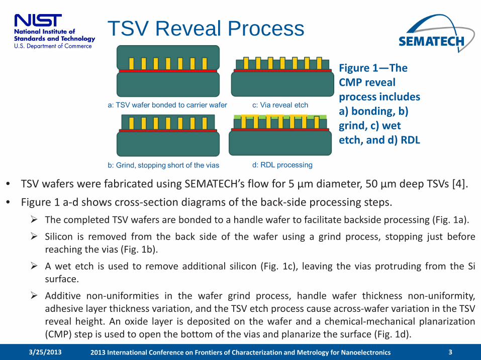
• TSV wafers were fabricated using SEMATECH’s flow for 5 µm diameter, 50 µm deep TSVs [4]. • Figure 1 a-d shows cross-section diagrams of the back-side processing steps.
The completed TSV wafers are bonded to a handle wafer to facilitate backside processing (Fig. 1a). Silicon is removed from the back side of the wafer using a grind process, stopping just before
reaching the vias (Fig. 1b). A wet etch is used to remove additional silicon (Fig. 1c), leaving the vias protruding from the Si
surface. Additive non-uniformities in the wafer grind process, handle wafer thickness non-uniformity,
adhesive layer thickness variation, and the TSV etch process cause across-wafer variation in the TSV reveal height. An oxide layer is deposited on the wafer and a chemical-mechanical planarization (CMP) step is used to open the bottom of the vias and planarize the surface (Fig. 1d).
Figure 1—The CMP reveal process includes a) bonding, b) grind, c) wet etch, and d) RDL
3 2013 International Conference on Frontiers of Characterization and Metrology for Nanoelectronics 3/25/2013
TSV Reveal Process
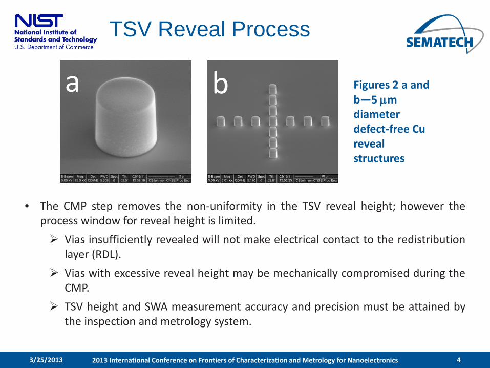
• The CMP step removes the non-uniformity in the TSV reveal height; however the process window for reveal height is limited. Vias insufficiently revealed will not make electrical contact to the redistribution
layer (RDL). Vias with excessive reveal height may be mechanically compromised during the
CMP. TSV height and SWA measurement accuracy and precision must be attained by
the inspection and metrology system.
Figures 2 a and b—5 µm diameter defect-free Cu reveal structures
a b
4 2013 International Conference on Frontiers of Characterization and Metrology for Nanoelectronics 3/25/2013
TSOM Simulations of 5 µm Diameter TSV’s
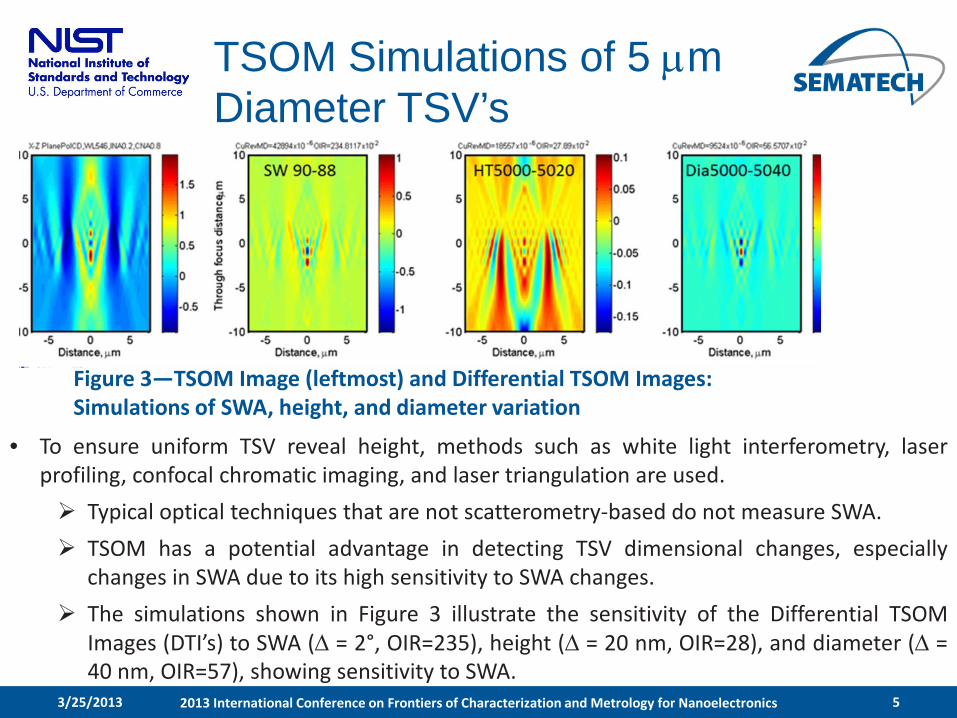
• To ensure uniform TSV reveal height, methods such as white light interferometry, laser profiling, confocal chromatic imaging, and laser triangulation are used. Typical optical techniques that are not scatterometry-based do not measure SWA. TSOM has a potential advantage in detecting TSV dimensional changes, especially
changes in SWA due to its high sensitivity to SWA changes. The simulations shown in Figure 3 illustrate the sensitivity of the Differential TSOM
Images (DTI’s) to SWA (∆ = 2°, OIR=235), height (∆ = 20 nm, OIR=28), and diameter (∆ = 40 nm, OIR=57), showing sensitivity to SWA.
5 2013 International Conference on Frontiers of Characterization and Metrology for Nanoelectronics 3/25/2013
Figure 3—TSOM Image (leftmost) and Differential TSOM Images: Simulations of SWA, height, and diameter variation

Profilometry Images of TSV’s
Figure 4—Profilometry images and heights for a 9-TSV reveal unit cell (a) and a single TSV (b). Also shown are feature anomalies.
• White light interferometry is a useful technique to obtain TSV reveal dimensions because it is high-speed, accurate, and has an adjustable depth of field.
• Profilometry measurements were averaged across a 9-TSV unit cell, as shown in Figure 4.
• Several significant feature such as a surface protuberance in the center of the TSV, edge lip, side wall roughness and recess into the Si at the bottom of the TSV are obtained by profilometry measurements.
b
6 2013 International Conference on Frontiers of Characterization and Metrology for Nanoelectronics 3/25/2013

Profilometry and TSOM Measurements of TSV’s
• TSOM was also used to image the 9-TSV unit cell in order to correlate the resulting differential TSOM images (DTI) to profilometry measurements of TSV height, diameter, and sidewall angle (SWA).
• Unit cells used to obtain DTI’s and average unit cell profilometry measurements were located in the adjacent die locations shown in Figure 5.
• Table 1 shows the average profilometry measurements for the 9-TSV reveal unit cell for left and right sidewall angle (LSW and RSW), diameter, and height in for reference die location 0,0.
Figure 5—TSV reveal die locations
Table 1—Profilometry measurements (SWA, diameter, and height averages from unit cell 0,0)
7 2013 International Conference on Frontiers of Characterization and Metrology for Nanoelectronics 3/25/2013
Experimental Profilometry and TSOM Measurements
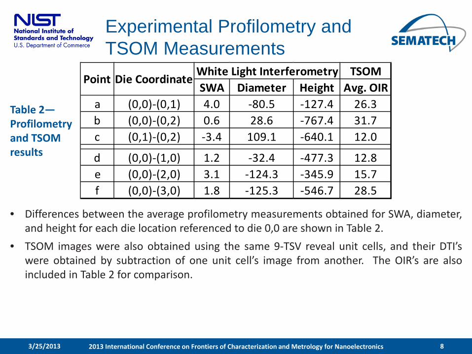
Table 2—Profilometry and TSOM results
TSOMSWA Diameter Height Avg. OIR
a (0,0)-(0,1) 4.0 -80.5 -127.4 26.3b (0,0)-(0,2) 0.6 28.6 -767.4 31.7c (0,1)-(0,2) -3.4 109.1 -640.1 12.0
d (0,0)-(1,0) 1.2 -32.4 -477.3 12.8e (0,0)-(2,0) 3.1 -124.3 -345.9 15.7f (0,0)-(3,0) 1.8 -125.3 -546.7 28.5
White Light InterferometryPoint Die Coordinate
8 2013 International Conference on Frontiers of Characterization and Metrology for Nanoelectronics 3/25/2013
• Differences between the average profilometry measurements obtained for SWA, diameter, and height for each die location referenced to die 0,0 are shown in Table 2.
• TSOM images were also obtained using the same 9-TSV reveal unit cells, and their DTI’s were obtained by subtraction of one unit cell’s image from another. The OIR’s are also included in Table 2 for comparison.
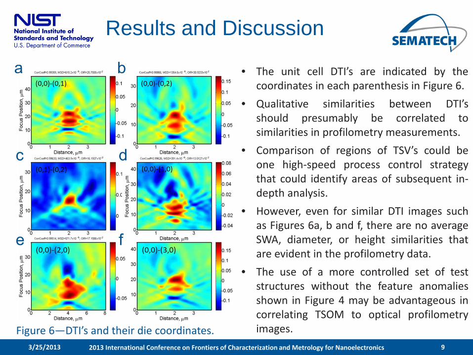
Results and Discussion
• The unit cell DTI’s are indicated by the coordinates in each parenthesis in Figure 6.
• Qualitative similarities between DTI’s should presumably be correlated to similarities in profilometry measurements.
• Comparison of regions of TSV’s could be one high-speed process control strategy that could identify areas of subsequent in-depth analysis.
• However, even for similar DTI images such as Figures 6a, b and f, there are no average SWA, diameter, or height similarities that are evident in the profilometry data.
• The use of a more controlled set of test structures without the feature anomalies shown in Figure 4 may be advantageous in correlating TSOM to optical profilometry images.
9 2013 International Conference on Frontiers of Characterization and Metrology for Nanoelectronics 3/25/2013
Figure 6—DTI’s and their die coordinates.
Summary
• TSOM has excellent sensitivity to SWA, CD, and height measurements, even at the nanometer scale, as shown by simulations of 5 µm diameter TSV structures.
• However, small feature anomalies such as those detected by profilometry make it difficult to compare profilometry measurements to TSOM DTI’s.
• These subtle features could generate strong optical interactions in the TSOM signal. • The use of a more controlled set of TSV’s may be advantageous in correlating TSOM to
optical images. • This process could be applied toward the construction of an image library that could
potentially identify dimension changes between features.
10 2013 International Conference on Frontiers of Characterization and Metrology for Nanoelectronics 3/25/2013
References
[1] Attota, R., Germer, T.A., and Silver, R.M., "Nanoscale measurements with a through-focus scanning optical microscope," Future Fab, 30, pp. 83-88, (2009). [2] Attota, R., and Silver, R.M., “Nanometrology using a through-focus scanning optical microscopy method,” Meas. Sci. Technol. 22, pp. 024002, (2011). [3] Attota R., “TSOM Method for Nanoelectronics Dimensional Metrology,” AIP Conf. Proc. 1395, pp. 57-63; 2011. [4] Olson, S.; Hummler, K., “TSV reveal etch for 3D integration,” 2011 IEEE International 3D Systems Integration Conference (3DIC), Jan. 31 2012-Feb. 2 2012.
11 2013 International Conference on Frontiers of Characterization and Metrology for Nanoelectronics 3/25/2013
Acknowledgements
The authors would like to thank John Kramar and Andras Vladar, at NIST, and Robert Edgeworth, Iqbal Ali, Craig Huffman, Steve Olson, Pete Moschak, Harry Lazier, and Elizabeth Lorenzini, at SEMATECH.
12 2013 International Conference on Frontiers of Characterization and Metrology for Nanoelectronics 3/25/2013