tools for the computer-aided design of multigigahertz
TRANSCRIPT

18 IEEE TRANSACTIONS ON APPLIED SUPERCONDUCTIVITY, VOL. 9, NO. 1, MARCH 1999
Tools for the Computer-Aided Designof Multigigahertz Superconducting
Digital CircuitsKris Gaj, Quentin P. Herr, Victor Adler, Andy Krasniewski,Fellow, IEEE, Eby G. Friedman, and Marc J. Feldman
Abstract—The realization of large integrated circuits dependsupon the application of computer-aided design (CAD) tools. Thispaper summarizes the results of a survey of CAD tools target-ing superconducting digital electronics. Five categories of tools:circuit simulators, circuit optimizers, layout tools, inductanceestimators, and logic simulators are discussed in detail. Withineach category, a comparison of several currently available CADtools is presented, and a tool which has been adapted for use ordeveloped at the University of Rochester is discussed in greaterdetail. In addition, tools for timing analysis as well as integrateddesign environments that permit the effective data interchangeamong various tools and support libraries of design modelsare discussed. Future tools for timing optimization, automatedlogic synthesis, and automated layout synthesis are shown tobe necessary for the design of superconducting circuits at thevery large scale of integration (VLSI) level of integration. Trendsregarding changes in the requirements for effective CAD toolsare discussed, and expected improvements to existing tools andfeatures of new tools currently under development are presented.
Index Terms—CAD, inductance extraction, layout, optimiza-tion, RSFQ, simulation, superconducting electronics.
I. INTRODUCTION
SUPERCONDUCTING digital electronics (SDE) comparesfavorably with all existing semiconductor technologies
when both speed and power consumption are considered [1],[2]. A major effort today in SDE focuses uponRapid SingleFlux Quantum (RSFQ)logic. Medium- to large-scale RSFQcircuits have been reported to operate with clock frequenciesabove 10 GHz, while 100-GHz RSFQ circuits should befeasible within the foreseeable future.
The complexity of semiconductor very large scale of inte-gration (VLSI) circuitry is a wonder of modern technology.Tens of millions of active transistors and additional passiveelements are systematically organized and fashioned suchthat the overall result of their individual operation providesa unified and coordinated function. This complexity is farbeyond the ability of a human mind to comprehend in all
Manuscript received April 25, 1998; revised October 30, 1998.K. Gaj is with the Department of Electrical and Computer Engineering,
George Mason University, Fairfax, VA 22030 USA.Q. P. Herr is with TRW Space & Electronics Group, D1/1039, Redondo
Beach, CA 90278 USA.V. Adler is with Sun Microsystems, Palo Alto, CA 94303 USA.A. Krasniewski is with the Institute of Telecommunications, Warsaw
University of Technology, Nowowiejska 15/19, 00-665 Warsaw, Poland.E. G. Friedman, and M. J. Feldman are with Department of Electrical
Engineering, University of Rochester, Rochester, NY 14627 USA.Publisher Item Identifier S 1051-8223(99)03354-0.
its detail. Rather, the development of semiconductor VLSIcircuits has been made possible by utilizing a large varietyof tools and methodologies which fall under the general nameof computer-aided design (CAD).The development of CADtools and design methodologies is a major research specialtyin the field of semiconductor integrated circuits.
The current situation insuperconductingdigital electronicsCAD is far less advanced. The level of integration of RSFQcircuits, although primarily limited by the relative immaturityof the process technology, is also distinctly limited by theavailable design tools. Future progress will depend on thedevelopment of more sophisticated CAD tools targeted toSDE. These tools are the subject of this paper; a companionpaper treats design methodologies for RSFQ circuits [3].
All superconducting logic schemes can be roughly classifiedas either flux-based, such as RSFQ, or voltage-state, such asMVTL. Voltage-state logic is a natural emulation of semicon-ductor technology in that data is encoded by steady voltagelevels. RSFQ logic is a new concept in which logic states“zero” and “one” are encoded using voltage pulses instead ofvoltage levels.
Conventional CAD tools used in the semiconductor industrycannot be directly applied to the design of superconductingdigital circuits. At the circuit and physical levels, the mainobstacles include a different basic active component (transistorfor semiconductor logic families versus Josephson junctionfor superconducting technology), a different basic passivecomponent (capacitor versus inductor), and different passiveand active interconnects (metal RC lines with buffers versusJosephson transmission lines and microstrips). At the logic andsystem levels the main problems include a different suite of ba-sic gates, different synchronization schemes, and significantlydifferent levels of influence of gates on each other. For SFQ-based logic, an additional problem is a different conventionfor representation of logic states.
Although certainly there are difficulties to adapting semi-conductor CAD tools for voltage-state superconducting logic,there are many more complications in adapting them forRSFQ. Several complete integrated design environments havebeen developed for superconducting voltage-state logic, forinstance [4] and [5], and there are many examples of circuitsconsisting of approximately 20 000 Josephson junctions whichhave been demonstrated [4].
The development of RSFQ logic began with the intuitivedesign of basic gates [6]–[9] and only recently has reached a
1051–8223/99$10.00 1999 IEEE

GAJ et al.: TOOLS FOR CAD MULTIGIGAHERTZ DIGITAL CIRCUITS 19
level of complexity where circuits with many tens of RSFQgates are successfully demonstrated at multigigahertz clockfrequencies [10]–[14]. The initial progress utilized tools andmethods developed specifically for RSFQ logic, which allowminimal automation. Together with the increasing complexityand growing variety of RSFQ circuits currently under develop-ment, design methods have evolved and new tools have beencreated to satisfy this need.
In the early stages of the development of RSFQ logic(1985–1992), the only tools in use were acircuit simulator(such as JSpice [15], PSCAN [16], or JSim) and a simplelayout editor (such as AutoCAD or Magic). Beginning in1993,circuit optimizers(such as MALT [17]) andinductanceestimators(such as Lmeter [18]) were introduced to increasethe yield of superconducting circuits and accelerate the designprocess, and the capabilities of circuit simulators and layouteditors were significantly enhanced. Also beginning in 1992,research on logic level simulation of RSFQ circuits wasinitiated [19]. This early research effort led to the developmentof more efficient tools for simulating RSFQ circuits at thelogic level [20].
Until very recently, tools for designing RSFQ circuits havebeen developed as separate components. These tools could notexchange data between each other and did not conform to stan-dards used by CAD vendors within the semiconductor circuitsindustry. Several groups have made an effort to develop theirown environments for the design of RSFQ circuits, based ona combination of commercially available, public-domain, andin-house developed tools [21]–[23]. Nevertheless, only a fewcoherent and integrated environments have been developed todate.
In part because of these deficiencies, the most complexRSFQ circuits are composed of roughly 2000 Josephsonjunctions and even at this scale they have required a con-siderable and tedious effort to realize [12], [24]. Furtherprogress, to higher clock rates and greater levels of integrationcomplexity, will require significantly more sophisticated CADtools. Nevertheless, the recent development of the rather small-scale circuits have prepared the way for RSFQ circuits ofdrastically ambitious performance and complexity which arenow envisioned.
In 1997, a large trial project began to explore the possibilityof building a petaflops (10 floating point operations persecond) scale supercomputer based on RSFQ logic, underthe title Hybrid Technology MultiThreading (HTMT) Archi-tecture [25], [26]. In principle, a petaflops system basedon RSFQ logic and other advanced technologies may berealizable within a ten-year time frame, far earlier than wouldbe possible assuming the evolutionary progress of classicalsemiconductor-based technologies [2], [25]. A single RSFQprocessor required for the HTMT architecture is expected tocontain several million Josephson junctions. This complexityis far beyond the ability of currently available CAD toolstargeted for developing medium-scale RSFQ circuits. Not onlymust tools for logic level simulation be adapted and enhanced,but also new tools for timing optimization, automated logicsynthesis, and automated layout synthesis will need to bedeveloped.
Current progress in the area of CAD tools for superconduct-ing digital electronics is driven by two primary issues:
• practical industrial-based projects aimed at developingmedium-scale specialized circuits for niche applications,such as analog-to-digital converters [24], [27], time-to-digital converters (timing digitizers) [28], [29], and digitalfilters [11], [12], [30];
• long range projects (such as HTMT) to apply RSFQto high performance high complexity general-purposecomputing [2], [25], [26], [31], [32].
In the first case, targeting for medium-scale applications, theexisting tools discussed in this paper offer improved accuracyand design efficiency sufficient for the majority of theseapplications. In the latter case, no tools and methodologies aresufficient to deal with the complexity of this target problem.Although currently the main obstacle on the way to the devel-opment of very large-scale superconducting digital circuits isthe immature fabrication technology, the lack of appropriatetools and methodologies may soon become a significant factorlimiting further progress, even if other technical challengeswere to be solved.
In Section II, the basic design flow for SDE circuits isreviewed. In Section III, a survey of existing tools for thedesign of superconducting digital circuits is presented. Thissurvey is followed in Section IV by a discussion of futuretools required for the development of superconducting VLSIcircuits. Trends regarding changes in design requirements,expected improvements to existing tools, and new tools underdevelopment are summarized in Section V.
II. BASIC DESIGN FLOW
A. Established Tools
The basic design flow for small- to medium-scale super-conducting digital circuits, illustrating the basic tools usedduring the design process, is shown in Fig. 1. The first stageof the design process, creating a junction-level schematicof the circuit from its functional description, has remainedunautomated and highly intuitive. After the initial structureof the circuit and values of the components are determined,the circuit is captured by theschematic editor. The schematiceditor is often integrated into a circuit simulator or layouteditor, but it can also work as a stand-alone tool or within alarger CAD environment. The netlist of the circuit is generatedautomatically by the schematic editor. The exact format ofthe netlist is determined by the requirement of the circuitsimulator. The most typical format accepted by the majorityof circuit simulators is the Spice notation [33]. For simplesuperconducting circuits, it is possible to create the netlist ofthe circuit manually and avoid the use of a schematic editor,but this process becomes cumbersome even for medium-scalecircuits.
In the next step, the designer chooses test input stimulisufficient to verify whether the circuit operates correctly. Thesestimuli can be either defined within a schematic editor asvoltage or current sources, or can be described in a textualnotation as a part of the netlist. The circuit is then simulated,

20 IEEE TRANSACTIONS ON APPLIED SUPERCONDUCTIVITY, VOL. 9, NO. 1, MARCH 1999
Fig. 1. Design flow for small- to medium-scale superconducting digitalcircuits.
verified, and modified iteratively until the correct operation forall input stimuli is obtained. In each iteration, the source offailure must be both determined and corrected. This processmay be simplified and quickened if the schematic editor andthe circuit simulator are closely integrated, and the circuitsimulator has features permitting localizing errors within acircuit.
Optimizing the circuit starts once the set of parameters forwhich the circuit operates correctly is determined. The purposeof the optimization process is to determine the optimumvalues of the parameters describing the components in thecircuits (e.g., the values of resistances, inductances, criticalcurrents, and bias currents), for which the circuit has thehighest probability to operate correctly after fabrication despitevariations in the fabrication process. Optimization is often themost time-consuming part of the design process. After theoptimization step is completed, the new parameter values areintroduced into the schematic.
The next step is to create a layout of the circuit correspond-ing to the optimized schematic. For superconducting circuits,this is done manually using alayout editor.The layout editortypically includes adesign rule checker (DRC)responsible forfinding any violations of the process design rules, such asthe minimum spacing between two layers. The DRC must becalibrated to work for a specific superconducting fabricationprocess (e.g., the Hypres, ten level, Nb/AlO /Nb trilayerprocess [34]).
Modern layout editors include a more powerful verificationtool, layout versus schematic (LVS)verification, integratedinto the layout process. The function of LVS verificationis to compare the original schematic of the circuit withthe equivalent circuit schematic extracted from the layout.In this way, electrical design errors created during layoutediting can be detected and fixed before the circuit is sentto fabrication. Electrical errors reported by LVS may also
Fig. 2. Design flow for large-scale superconducting digital circuits.
result from extracting parasitic components, such as parasiticinductances. If these parasitic inductances are meaningful, e.g.,their values are greater than some predetermined threshold,the parasitic impedances must be added to the schematic.Once these parasitic inductances are included within the circuitschematic, the figures of merit used during optimization (suchas the critical margin or expected yield of the circuit) maydegrade. These figures of merit must be recomputed, and ifthe change is meaningful, the circuit must be reoptimized,followed by modifications to the circuit layout. The entireprocedure may need to be repeated several times until nosignificant differences between the layout and the schematicare detected by the LVS checker, and the circuit is found tobe sufficiently robust against parameter variations.
B. Emerging Tools and Extensions
For more complex superconducting digital circuits the basicdesign flow used for small-scale circuits is not satisfactory.The computer time required to simulate the circuit, and thenumber of parameters which must be included in optimization,increases to the point where it is inefficient or even computa-tionally infeasible to directly scale up the small circuit designprocedure. This problem was confronted long ago in semi-conductor digital electronics. Large semiconductor circuits aredesigned at the logic level rather than at the device level. Inthis approach, the circuit is constructed using a limited setof previously developed building blocks. These blocks can bebasic logic gates or they can be larger subcomponents. Thebasic design flow for large-scale superconducting circuits isillustrated in Fig. 2. Compared to the design process for small-scale circuits, the primary difference is the replacement of acircuit simulator by a logic simulator and the replacement ofa yield optimizer by a timing optimizer.
Logic simulation for superconducting circuits can be per-formed usinglogic simulatorsdeveloped for semiconductor
GAJ et al.: TOOLS FOR CAD MULTIGIGAHERTZ DIGITAL CIRCUITS 21
electronics. For superconducting voltage state logic the useof existing logic simulators is straightforward because thesame convention is used to represent the logic states and bothtechnologies use a similar suite of basic gates. For RSFQ logic,existing logic simulators with their libraries of standard gatescannot be applied directly. The main problems are:
• the different conventions used to represent logic statesbased on pulses rather than voltage levels;
• a different suite of basic gates including clocked RSFQelementary gates instead of combinational semiconductorgates;
• the strong influence of RSFQ gates on each other thatmay affect timing parameters and thus accuracy of thesimulation.
Despite these difficulties, existing simulators have beenadapted to work with RSFQ logic. This was achieved bycreating model libraries of RSFQ gates that accurately describethe behavior of RSFQ gates and at the same time can besimulated using traditional semiconductor-based simulationtools. The most straightforward technique for creating suchmodels is the use of ahardware description language (HDL)such as Verilog HDL or VHDL [20].
To be useful for timing analysis of a large circuit, RSFQgate models must include information about timing parameters,such as the propagation delay, the hold time, and the setup time[19], [35], [36]. Values of these parameters must be foundusing circuit (junction) level simulation. This is straightfor-ward, but nevertheless, doing all of the simulations requiredto manually determine the hold time or setup time is both time-consuming and cumbersome. Therefore, either existing circuitsimulators must be extended to permit these timing parametersto be determined or specialized tools closely integrated withthe circuit simulators need to be developed to accomplish thesame purpose.
Logic simulation by itself can be used to verify the correctfunction of the circuit and to detect any gross timing errors.Nevertheless, it does not provide the designer with informationabout the optimum values of the interconnect delays withinthe circuit. To obtain these values, atiming optimizermustbe developed. This tool requires information about the circuitstructure, assumed timing scheme, circuit layout limitations,and variations of timing parameters of the basic cells tocalculate the optimum interconnect delays. To be completelygeneral, the tool would need to accept both synchronous andasynchronous timing schemes.
Versions of all of these aforementioned tools have beendeveloped but are not presently in widespread use. The primaryreason is the small number of research groups involved in thedevelopment of large-scale RSFQ circuits, while most researchgroups deal with only small-scale circuits and highly repetitivestructures. Another primary obstacle is the lack of a generallyaccepted theory regarding how best to properly model timingin RSFQ circuits.
C. Future Tools
When the complexity of superconducting circuits growsto a VLSI level, such as a million junctions on a single
chip, these emerging tools will be grossly inadequate.One primary concern is layout editing. Even for circuitswith thousands of Josephson junctions, manual editingis grueling and excessively time-consuming. For largercircuits, the time necessary for editing quickly becomesprohibitive. The only solution is to develop tools forautomated layout synthesis.Unfortunately, the existing toolsappropriate for semiconductor circuits cannot be easilyadapted because of differences in implementation andin the characteristics of interconnects between these twotechnologies.
The other area where automation will certainly becomeindispensable for VLSI circuits is logic synthesis. Currentmethods, based mainly on designer intuition, do not scalewell for larger circuits with little regularity or a large va-riety of gate types. Tools forautomated logic synthesisofsemiconductor circuits cannot be easily calibrated to RSFQlogic. The primary obstacle is that RSFQ gates are clocked, notcombinational, and that the synthesis process should includethe clock distribution network.
None of these tools have been developed to date forsuperconductors. Researchers have hardly begun to investigatethe feasibility of calibrating semiconductor CAD tools for usein automated logic and layout synthesis.
III. SURVEY OF EXISTING SDE CAD TOOLS
In this section, the results of a survey of superconductingdigital electronics design tools is presented (Tables I–VI). Fivebasic categories of existing SDE design tools, currently in useby major SDE university and industry groups worldwide, havebeen considered. Although some of the tools are specific toRSFQ logic, note that the majority of the tools can be used forother types of superconducting logic. A significantly expandedversion of this survey has been published on the World WideWeb in the form of interactive tables [37]. It is intended thatthe survey will be continued in the future and that the website will be updated as the technology evolves. The reader isencouraged to study the more detailed version of the tablesavailable on the web, updated to represent the most recentstate of SDE CAD technology.
In this paper, the features of all major existing tools ineach of the five categories of SDE CAD tools are reviewedand compared. Then, as an example, the particular toolsdeveloped, calibrated, and/or adapted for use at the Universityof Rochester are discussed in greater detail. It should beunderstood that although the Rochester group has made aneffort to select or develop the best tool in each category,the final solutions described in this article have been clearlyinfluenced by historical, economical, and educational factors,apart from purely technical considerations. No superiorityof Rochester tools over equivalent tools developed or usedby other groups is implied, and the detailed description ofthe Rochester toolset should be treated as an example ofan integrated design environment for superconducting digitalcircuits, rather than a set of recommendations for use by otherSDE groups.

22 IEEE TRANSACTIONS ON APPLIED SUPERCONDUCTIVITY, VOL. 9, NO. 1, MARCH 1999
TABLE IFEATURES OF EXISTING CIRCUIT SIMULATORS
A. Circuit Simulator
1) Survey of Existing Tools:A variety of circuit simulatorshas been either extended to work for superconducting circuitsor has been written exclusively to simulate superconductinglogic, as shown in Table I. The first group includes modifi-cations of Spice (such as Jspice3 [15], [33], WRSpice, Spice3f4, HSpice), and extensions of other circuit simulators suchas Eldo [38]. The second group includes original simula-tors, such as JSim developed at the University of Berkeley,PSCAN developed at Moscow State University [16], rewrittenand extended at SUNY Stony Brook [23], WinS written byKaplunenko, and JULIA developed by Shevchenko. Numerousproprietary modifications have been added to JSim at DERA(Defense Evaluation and Research Agency) in the UnitedKingdom.
A primary difference between these two groups of simu-lators concerns user documentation, user support, and errorhandling. Simulators written exclusively for superconductinglogic have been developed at universities for noncommercialpurposes and are currently available in the public domain. Todate, documentation for these simulators is scarce, user supportis not guaranteed, and error handling is often inadequate.
In terms of accuracy and speed, there seem to be nofundamental differences among the simulators surveyed inTable I. The accuracy offered by these tools is adequate for thedesign of digital and mixed-signal superconducting circuits.No reliable speed comparison of these simulators has beenperformed. This comparison would require the development ofa set of benchmarks and simulations performed on the sameor equivalent type of machines. An additional complication isthe different definition of parameters controlling the accuracy
of the simulators. A comparison of speed can be meaningfulonly if these parameters are set to values corresponding to thesame simulation accuracy. Default values of accuracy-relatedparameters are often different for various simulators.
One clear distinction between two groups of circuit sim-ulators is the choice of a basic internal variable. In JSim,Eldo, and all Spice-based simulators, nodal voltages are usedas basic variables; phases of Josephson junctions are derivedfrom these voltages. On the other hand, in PSCAN, JULIA,and WinS all of the superconducting circuit equations aresolved with phase as the basic variable; voltages are computedonly after completing the Newton iterations required duringthe numerical analysis. The effect of this difference on theaccuracy or speed of the simulators appears to be noncritical,but to the authors’ knowledge, this difference has not beenquantitatively assessed to date.
Additionally, some simulators, e.g., PSCAN, have a built-in microscopic (“Werthamar”) model of Josephson junctions[39], [40], [16]. This feature may be necessary to correctlymodel submicron Josephson junctions in new process tech-nologies, currently under development.
Another difference arises from the use of an internal versusan external Josephson junction model. An internal model isbuilt into the source code of the simulator, while an externalmodel is defined by the user using specialized notation andis invoked as a macro. Although both models are typicallyfunctionally equivalent, leading to the same simulation resultsand accuracy, the difference in speed can be substantial. Theuse of an external Josephson junction model (as in HSpiceand Eldo) may slow down the simulation by one or even twoorders of magnitude [41]. On the other hand, the capability

GAJ et al.: TOOLS FOR CAD MULTIGIGAHERTZ DIGITAL CIRCUITS 23
of using external models significantly simplifies the processof adapting commercial semiconductor circuit simulators foruse with superconducting logic. The reduction in simulationspeed may be further justified by additional simulation modesand by greater compatibility with the powerful capabilitiesof commercial simulators, such as Monte Carlo analysis ormixed-mode simulation.
In summary, all of the available circuit simulators appear tooffer accuracy and speed sufficient for the transient analysis ofsmall- and medium-scale superconducting circuits. The choiceof simulator may depend on:
• additional operational modes, such as Monte Carlo anal-ysis, mixed-mode simulation, or noise simulation [42],[43];
• an associated or built-in optimizer;• documentation and user support;• user interface;• operating system and hardware platform;• availability and price.
At the time of writing,JSpice3, WRSpice,andPSCANare themost widely used circuit simulators by groups involved in thedesign of medium- to large-scale RSFQ circuits. JSim is themost popular simulator among groups dealing with the designof small-scale superconducting circuits and structures.
2) University of Rochester Tools:The basic circuit simu-lator used at Rochester isJSpice3from Whiteley Research,Inc. Its primary advantages include good documentation, usersupport, low price, high speed, and large user base. Thesimulator has an internal Josephson junction model, permitstwo-dimensional (2-D) margin analysis, and has a compre-hensive script language and a user-friendly graphical userinterface. JSpice3 is fully compatible with Spice3 and thereforecan be used to simulate hybrid semiconductor–superconductorcircuits. It is also compatible with its successor WRSpice. TheRochester in-house developed tools, such as MALT for circuitoptimization and TAN for timing parameter extraction, havebeen based on JSpice3 and exploit the capabilities of its scriptlanguage. Both of these tools work without modifications withWRSpice.
B. Optimizer
1) Survey of Existing Tools:As opposed to other tools suchas simulators and layout editors, the existing circuit optimiz-ers for superconducting digital circuits have primarily beendeveloped at universities, have been written from scratch,and are either proprietary or available in the public domain.This background results from the fact that optimizing su-perconducting digital circuits, in particular RSFQ gates, issignificantly different from optimizing semiconductor gates.The most important factors that contribute to this differenceare:
• superconducting RSFQ gates are based on two-terminalJosephson junctions versus three-terminal transistors usedin semiconductor logic; this characteristic complicates thedesign of a single gate, decreases the input and outputimpedance, and increases the sensitivity of the circuit tovariations of the component parameters;
• certain parameters that are optimized such as junctionsizes, inductors, or bias currents are unique to supercon-ducting circuits;
• the fabrication process is significantly different, and pa-rameter variations are larger in currently immature su-perconducting foundries as compared to sophisticatedmultibillion dollar semiconductor fabrication facilities.
Additionally, semiconductor-based digital circuits are rarelydeveloped as purely custom circuits (exceptions includeRAM’s and microprocessors); instead, standard libraries areused to build most digital circuits. Therefore, it is typical thata designer of a semiconductor logic circuit may never usea circuit optimizer. On the contrary, RSFQ cells are customdesigned for different applications. The first attempts to usethe same basic RSFQ cells in multiple designs have onlyrecently been accomplished by several industry groups, androbust libraries of such gates have yet to be developed [28],[44]. Therefore, efficient circuit optimization remains one ofthe critical steps in the development of RSFQ circuits.
The robustness of RSFQ gates can be reliably quantifiedby circuit yield, the ratio of the number of circuits operatingcorrectly to the total number of fabricated circuits. If it isassumed that the random distribution of the parameters char-acterizing the fabrication process is close to Gaussian and thattheir standard deviations are well characterized, the yield of acircuit can be determined using a Monte Carlo analysis. Thistechnique requires simulating the circuit multiple times withall parameters chosen at random according to their respectiverandom distributions. Although this strategy for measuringcircuit robustness is clearly the most straightforward andaccurate, it is also computationally expensive.
Therefore, a simpler measure, called thecritical margin, hasbeen adapted by many groups [45]. Individual margins of aspecific parameter are defined as the difference between theupper and lower limits of the operating parameter for whichthe circuit operates correctly and the nominal value of thisparameter, while other parameters are held at their nominalvalues. The critical margin is the smallest of the individualmargins calculated for all parameters. One advantage of usingthe critical margin as a measure of circuit robustness isthat it can be efficiently computed, e.g., applying a binarysearch to each individual parameter. It provides an intuitivelydirect technique for optimizing the circuit by centering eachparameter within its operating range [45]. The assumption isthat when all parameters are centered, then the parameters areat their optimum values and the critical margin is that mostlikely to cause a circuit fault. This would in fact correspondto the maximum yield point if all the parameter effects wereindependent of each other, but this is never the case. Anotheradvantage is the possibility of experimental verification ofindividual margins for one type of parameter—the bias current.
There is no proven correlation between circuit yield andcritical margin. On the contrary, it has been shown that thereexist hypothetical circuits for which the point of optimum yieldis relatively far from the point of optimum critical margin[17]. Despite this, it is commonly believed that for practicalRSFQ circuits these measures are positively correlated, andoptimizing the circuit with respect to critical margin improves

24 IEEE TRANSACTIONS ON APPLIED SUPERCONDUCTIVITY, VOL. 9, NO. 1, MARCH 1999
TABLE IIFEATURES OF EXISTING CIRCUIT OPTIMIZERS
1The computation time increases with the number of parameters or the optimization becomes less effective (smaller improvements of the figure of merit).
circuit yield. A quantitative analysis of this relationship wouldrequire defining a set of benchmark circuits, optimizing thesebenchmark circuits using both figures of merit, and comparingthe yield of the final circuits using a Monte Carlo analysis.
Existing circuit optimizers, shown in Table II, can be di-vided into two distinct groups on the basis of the definitionof the figure of merit being optimized. One group uses thecritical margin as a figure of merit and includes COWBOY[23], rtry [46], and WinS. COWBOY is currently an integralpart of the PSCAN simulation environment [23], while rtry is astand-alone tool using JSim for simulation. The second groupincludes MALT developed at the University of Rochester [17],[47], [48], XOPT developed at the University of Ilmenau(Germany) [49], [50], and ABAK [51] developed at theUniversity of Karlsruhe (Germany). All of these tools useyield as the figure of merit being optimized. MALT employsJSpice3 or WRSpice for simulation, XOPT is based on Eldo,and ABAK works with Spice 3f4.
Optimizers using yield as a figure of merit can be furtherdivided depending on the type of optimization algorithm beingused. ABAK and XOPT use statistical algorithms such as theCenter of Gravity Method (CGM). This algorithm determinesan optimum set of nominal parameter values by:
• choosing a number of parameter sets around an initial(temporary) operating point;
• simulating the circuit for each set of parameters to deter-mine for which of these sets the circuit operates correctlyand for which it fails;
• moving the temporary operating point based on the aver-age position of the pass–fail parameter sets.
MALT and XOPT use a deterministic algorithm calledthe method of inscribed hyperspheres(or simplicial approx-
imation) developed by Director [52], [53]. The algorithmaims at inscribing the largest possible hypersphere within amultidimensional operating region of the circuit. After thealgorithm terminates, the optimum value is chosen at the centerof the inscribed hypersphere.
Heuristic algorithms are used to optimize the critical marginin COWBOY and rtry. These algorithms are highly efficientand have no clear limitations on the number of parameters. Theadvantages of the method of inscribed hyperspheres includeits speed and accuracy. The disadvantages are the limitationon the number of parameters optimized in a single programrun, and the requirement that the shape of the operatingregion be convex. These disadvantages can be easily overcomeby properly choosing the parameter sets or transforming theparameters into a logarithmic space, as described in [17] and[47].
Statistical methods, in principle, can be applied to an arbi-trary number of parameters being simultaneously optimized;nevertheless, the final result of the optimization proceduredepends strongly on this number. As a result, it is difficultto assure sufficient accuracy (and thus close to the optimumchoice of all operating parameters) and reasonable efficiencyfor a large number of parameters. For a small number ofparameters, the method of inscribed hyperspheres is clearlymore efficient. Further research, considering both optimizationspeed and post-optimization yield, is required to quantitativelycompare both methods.
The other important distinction between these various opti-mization programs, independent of the figure of merit and op-timization algorithm, is the manner of specifying thepass–failcriteria for a given circuit. Pass–fail criteria are used by theoptimizer to distinguish between correct and incorrect circuitoperation.

GAJ et al.: TOOLS FOR CAD MULTIGIGAHERTZ DIGITAL CIRCUITS 25
Two basic ways of describing pass–fail criteria are currentlyin use among available optimizers. In MALT and WinS,pass–fail criteria are generated automatically on the basis ofthe simulation results for an initially correct set of parameters.In COWBOY/PSCAN, XOPT, and ABAK, a special HDL isused to describe the correct operation of the circuit. Variouslanguages are used for this purpose: PSCAN uses a custom-designed notation called SFQHDL [54], XOPT employs asubset of VHDL called HDL-A [50], and ABAK makes useof the general purpose object-oriented programming languageC++ [51]. The exact rules for describing correct circuit be-havior vary from notation to notation. Typically, a user mustdescribe the exact order in which junctions switch within thecircuit, thereby specifying the behavior of all internal nodeswithin the circuit.
Both approaches have their advantages and disadvantages.Automatic generation of pass–fail criteria is extremely fastand convenient. On the other hand, no support is provided todetermine the correct set of parameters.
Manual specification of pass–fail criteria using HDL’s maybe cumbersome, particularly for medium to large-scale circuits.On the other hand, at least in principle, once properly preparedthis specification can be used to search for the initial set ofoperating parameters and/or support localization of errors.
Additional factors in choosing a circuit optimizer includea user-friendly interface, documentation, and user base.Presently, only two optimizers are in use by more than oneresearch group,MALT and COWBOY/PSCAN.
2) University of Rochester Tools:The MALT optimizerwas developed at the University of Rochester from 1993to 1994. Since then, MALT has been transferred to severaluniversity and industrial groups. It has also been extensivelyused within the Rochester group to design about 20 basicRSFQ cells [12], [17], [47].
A short justification of several decisions made during thedevelopment of MALT, and a short review of its features arediscussed below. MALT consists of three separate programswritten in C, where each program performs, respectively, the:
• automatic generation of pass–fail criteria (init);• one-dimensional (1-D) and 2-D operating range analysis
(marg);• optimization (opt).
The C programs constituting MALT are supported by a set ofJSpice3 scripts.
MALT was originally written to work with JSpice3 and isalso compatible with the current version of WRSpice. The coreof the optimization program (opt) can be adjusted to work withother circuit simulators.
MALT optimizes the yield of the circuit, using a determinis-tic method of inscribed hyperspheres. In the authors’ opinion,MALT offers a better tradeoff between the optimization effec-tiveness and computational efficiency than other optimizationtools currently available. MALT provides a more optimal resultthan programs based on critical margin optimization and ismore efficient than statistical methods aimed at providing anequivalent optimal solution.
Fig. 3. MALT: Generating pass–fail criteria forsynchronous circuits.Positions of checkpoints are determined on the basis of the CHECK-POINT_RATIO, which defines the relative position of each checkpointin the clock cycle.
One of the distinct features of MALT is the capability togenerate pass–fail criteria automatically on the basis of a singlesimulation of the circuit for correct operating parameters.This capability is performed by defining time windows wheneach specified junction must undergo a 2phase change.The position of these windows is determined automaticallyon the basis of the simulation results for a correct set ofoperating parameters as well as a set of numerical parametersprovided in the MALT configuration file [48]. The algorithmfor determining the positions of these checkpoints (those pointswhere the value of the phase at the output nodes is verified) isdifferent for synchronous (clocked) and asynchronous circuits.For synchronous circuits, the checkpoints are set at a givenpercentage of a clock cycle, typically close to the end ofthe cycle, as shown in Fig. 3. By applying this convention,any realistic variation in the clock-to-output delay does notinfluence the outcome of the phase comparison. For asyn-chronous circuits, the checkpoints are set a certain time intervalbefore and after the nominal position of the output pulse, asshown in Fig. 4. This procedure permits accommodating forlimited variations in the position of the output pulses. Thisconvention was later adapted in WinS, where additionally theuser of the program can interactively change the positions ofthe checkpoints relative to the output waveforms.
Two main problems have been reported by users of MALT.First, the user interface is textual and requires preparingseveral input files for each circuit. Second, the selection of thecircuit parameters subject to optimization during a particularoptimization run must be done manually and intuitively onthe basis of criticality and interrelations among the variousparameters.
To address the first problem, MALTTool, a graphical userinterface for all MALT programs is under development. Thisinterface should greatly simplify the preparation of the inputdata and the interpretation of the final results.
The second problem, however, is intrinsic to this technique.The algorithm itself limits the number of parameters capableof being simultaneously varied during the optimization toeight or at most nine. Running on an Ultra Sparc, an eight-

26 IEEE TRANSACTIONS ON APPLIED SUPERCONDUCTIVITY, VOL. 9, NO. 1, MARCH 1999
TABLE IIIFEATURES OF TOOLS FOR LAYOUT EDITING AND VERIFICATION
dimensional (8-D) optimization of a circuit containing 20junctions requires about 10 min, a nine-dimensional (9-D)optimization requires from 1 to 2 h. Even the simplest RSFQgates have more than eight or nine parameters. To cope withthis problem, several parameters at a time can be optimizedin an iterative process. This method is effective but has somelimitations. The most critical parameters must be determinedand included in each successive optimization. Otherwise, thefigure of merit will change from one optimization to thenext, and the set of parameter values will not converge tothe optimum solution. Second, concavities may exist in theoperating region, and the parameter values may not convergeto the optimum. These problems can be overcome throughthe use of optimization techniques described in [17] and[47], which provide general guidelines for choosing propersets of parameters for successive optimizations. Nevertheless,the final choice of the parameter sets is circuit specific andknowledge of the circuit operation can significantly enhancethe efficiency of the iterative optimization.
C. Layout Tools
1) Survey of Existing Tools:Most of the layout tools usedto design superconducting circuits (see Table III) arecommer-cial semiconductorCAD tools. This outcome has occurredbecause semiconductor layout tools are sufficiently generalto permit relatively easy calibration in order to accommodatedifferent types of technologies. The calibration is often re-duced to writing appropriate technology files, specific for agiven fabrication process. In addition, layout tools are amongthe most complex and time-consuming to develop, and thecurrent scope of SDE research and design effort worldwidedoes not justify development of such tools specifically forsuperconducting technology.
Price may be a decisive factor in selecting a layout tool.In particular, the high cost of the Cadence toolset, includingVirtuoso (layout editor) and Diva (layout verification), is adeterrent to small industry research groups. On the other hand,the relatively loweducationalprice together with the elaboratecapabilities of Cadence have caused this toolset to become
the most commonly used among university researchers. Thissituation is particularly disadvantageous for small companiesthat cannot afford Cadence, because they cannot anticipate thatuniversities will calibrate other less expensive tools. Lowercost alternatives to Cadence are such commercial tools as Xicand L-Edit or public domain programs such as Magic and Kic.
The basic part of each layout tool, the layout editor, isdifficult to compare. The most important feature, a user-friendly interface is often a matter of personal preference.The public domain Magic editor has the disadvantages that itonly permits Manhattan structures and it applies old-fashionedpixel-oriented (versus object) graphics. Larger and more objec-tive differences exist in the area of layout verification. Thesedifferences concern tools for
• DRC;• electrical rule checking (ERC);• LVS.
Most of the layout tools include aDRC. This capability isresponsible for reporting violations of design rules such as theminimum spacing between two layers, the minimum width of agiven layer, or the minimum overlap of one layer outside of thesecond layer. AnERCdetects problems such as power/groundshorts and unconnected floating nodes. As similar rules mustbe verified for CMOS and other semiconductor processes,superconductive-based design and electrical rules can be easilyincorporated into existing commercial semiconductor layouttools.
More difficult is the calibration of a final verificationprocess—LVS comparison. The purpose of LVS verification isto compare the original circuit schematic with the schematicextracted from the circuit layout. In the first phase, a circuitextractor identifies all devices in the layout and the connectionsbetween the devices. As a result, a netlist of the extractedcircuit is created. Optionally, values of the device parametersare calculated during extraction and included in the netlist.In the second phase, a netlist obtained from the originalschematic is automatically matched with the netlist extractedfrom the layout and differences in connectivity and parametervalues are reported.

GAJ et al.: TOOLS FOR CAD MULTIGIGAHERTZ DIGITAL CIRCUITS 27
Unmodifiedsemiconductortools can typically perform ex-traction of transistors, resistors, and capacitors, but lack thecapability to extract inductances, particularly inductances ofsuperconducting structures. As a result, special extensionshave been added to Cadence Diva at SUNY Stony Brookand the University of Rochester. Stony Brook extensionsemploy Lmeter to extract inductor values, while the Rochesterextensions use a simplified approach based on computing thenumber of squares constituting an inductor and multiplying itby an average inductance per square. The number of squaresconstituting corners, tees, and vias are adjusted according tothe scaling factors used for resistances.
LVS comparison using Xic is limited to checking for correctcircuit connectivity. An additional interface from RSFQ, Inc.permits calculating values of inductances using Lmeter. Theauthors are not aware of any other tool currently being cali-brated to permit LVS verification of superconducting circuits.As a result,Cadenceand Xic are the primary candidates forlayout tools for the design of SDE circuits, with Cadenceprimarily being used by universities and large companies andXic aimed at smaller industrial research groups.
2) University of Rochester Tools:The Cadence layout toolpackage was adapted at Rochester in 1994 due to its superiorityover the previously employed Magic and L-Edit and its rela-tively low educational price for the entire toolset. This was thebeginning of an effort to create an integrated environment forthe design of large-scale RSFQ circuits. The Cadence toolsetincludes other tools such as a library manager, schematiceditor, two logic simulators, and an interface to various circuitsimulators, thereby providing an excellent framework for anintegrated design environment.
Initially, technology files for the Hypres fabrication processwere developed to permit usingCadence Virtuosoas a layouteditor for superconducting circuits. These technology fileshave since been extended to enable DRC and ERC usingCadence Diva, based on the Hypres design rules [34]. Fi-nally, parameter extraction and LVS verification based onCadence Diva were also added and extensively tested in1996 [21].
Two features of the extraction and LVS capabilities areworth mentioning. First, the precision of the parameter ex-traction is: 1% for junction areas, 2% for shunt and biasresistors, and 10% for significant inductors. Secondly, allsignificant inductors in the physical layout must be markedbefore extraction using a special dummy layer. This addedinformation prevents extracting parasitic inductances not ap-pearing in the schematic, which would make the comparisonwith an original schematic unsuccessful. The user must specifywhich parasitic inductances to extract, and these inductancesare introduced manually into the circuit schematic. The dummylayer is also necessary due to the relative inaccuracy ofthe extraction procedure for small inductances. For typicalparasitic inductances, the extraction error may easily exceed50%. No components other than inductors require a dummylayer.
These extensions to the Cadence layout tools are availablein the public domain. Future plans include increasing theaccuracy of the inductance extraction procedure.
Fig. 4. MALT: Generating pass–fail criteria for asynchronouscircuits. Positions of checkpoints are determined on the basis ofMAX_DELAY_VARIATION, which determines the distance betweeneach checkpoint and a nominal position of an SFQ pulse at the outputof the circuit.
D. Schematic Editors
Schematic editors are usually associated with circuit simu-lators or layout tools. This function is provided at Rochesterby the Cadence Composer. Customizing this editor for RSFQlogic requires the design of a library of symbols for the basiccomponents of RSFQ circuits such as Josephson junctions,inductors, resistors, and voltage and current sources. One ofthe unique features of this schematic editor is the capability toexport and import data in Electronic Design Interchange For-mat (EDIF) [55], which is the standard textual notation usedto transfer schematics among various design environments.
E. Inductance Estimator
1) Survey of Existing Tools:There are a variety of tools forestimating the inductance of superconducting structures, asshown in Table IV. These tools include both commerciallyavailable packages, such as Maxwell and Sonnet em, as wellas public domain tools such as Fast Henry and Lmeter.
The primary distinction between these inductance estimatorsis the type of algorithm used. Three-dimensional (3-D) meth-ods are in principle more accurate, but are typically quite slow.Two-dimensional methods introduce some computational in-accuracies but are significantly faster than the 3-D methods.There also exist simple programs, such assline, based onapproximate 2-D analytical formulas [56]. These primitivetools can only be used for estimating the inductances of simplemicrostrip lines.
In 1996, a survey regarding the accuracy of existing toolsfor inductance estimation was initiated [57]. The results ofthis survey were published on the web and are summarizedin Table V. The survey solicitation letter [57] specifies thegeometry of seven common structures, which roughly complywith the Hypres design rules [34]. The results submitted byvarious researchers use ten different methods and programs.The 3-D programs, Fast Henry [58], Sonnet em [59], andMaxwell [60], are in close agreement. For microstrip lines, theresults obtained using these programs differ from each otherby no more than 1%; for three other structures, two corners

28 IEEE TRANSACTIONS ON APPLIED SUPERCONDUCTIVITY, VOL. 9, NO. 1, MARCH 1999
TABLE IVFEATURES OF EXISTING INDUCTANCE ESTIMATORS AND EXTRACTORS
and one via, the difference is no more than0.02 pH; andfor one more structure, “via with spreading,” the differencedoes not exceed 0.04 pH. The difference between these resultsis substantial for only one structure, the crossover. Thisinconsistency is possibly due to a difference in interpretingthe structure description.
Lmeter [18] provides less accurate results, including a 5%difference in the inductance of microstrip lines; less than 0.1pH difference for the corners and the via; and less than 0.2 pHdifference for “via with spreading” compared to the averageresults generated by the 3-D programs. Lmeter estimationsshould be sufficiently accurate for most applications, andthe program can be further calibrated on the basis of 3-Dsimulations or test measurements based on a broad sampleof experimental data. Several other inductance estimationprograms are described in [61]–[65].
Despite its inaccuracies,Lmeter is the most widely usedtool to estimate inductance. Its primary advantages are highspeed and the ability to accept a description of the inductancestructure in the form of a standard CIF file which is generatedby most layout editors. Most 3-D programs are much slower,and only one, Sonnet em, accepts the standard GDSII filegenerated by many layout editors. Interfaces for CadenceVirtuoso and Xic have been written to extract inductances andprovide an LVS comparison based on Lmeter.
2) University of Rochester Tools:The method used atRochester to estimate and layout inductances combines thehigh accuracy of 3-D methods with instant access [58]. FastHenry is used to precompute values of inductances for mosttypical widths and a large range of lengths of microstriplines, for three basic combinations of layers in the Hypresfabrication process. The inductances of intermediate length
microstrip lines are then found by linear interpolation. Thesame procedure is repeated for different dimensions of corners,tees, and vias. All precomputed results have been collectedin a look-up table, and a graphical user interface (GUI) toolIcalc has been developed to access this table. Icalc determinesthe dimensions of a structure corresponding to the value of aninductor as well as a value of an inductance for a particularstructure.
Icalc unlike Lmeter cannot be used to automatically extractinductance values from a geometric layout. The only automaticinductance extraction procedure currently implemented in theRochester design environment is based on calculating thenumber of squares of a structure and multiplying the numberof squares by an average inductance per square for a givencombination of layers. Because of the inaccuracy involved inthis procedure, small errors (10%) may remain unreported.
In the authors’ opinion, the designer’s errors introducedto inductances during layout editing are rare, and thereforetheir effect on a final design is less critical than that ofthe systematic errors introduced to all circuit inductors byusing a less accurate 2-D algorithm to calculate the inductordimensions.
F. Logic Simulator
1) Survey of Existing Tools:The capabilities and advan-tages of using logic level simulation in the design of largeRSFQ circuits was first identified by Krasniewski [19]. From1992 to 1993 he developed at the University of Rochestera library of RSFQ cells based on Design Works, a standardlow-cost semiconductor logic simulator. As Design Worksdoes not support behavioral models of gates in a HDL, RSFQcells are modeled using an equivalent schematic description.

GAJ et al.: TOOLS FOR CAD MULTIGIGAHERTZ DIGITAL CIRCUITS 29
TABLE VRESULTS OF THEINDUCTANCE STRUCTURE RODEO. (a) ABSOLUTE RESULTS AND (b) RELATIVE ERRORS WITH REGARD TO THE MOST LIKELY ANSWER
(a)
(b)
Fig. 5. URSULA: Equivalent schematic description of the confluence buffer composed of standard semiconductor gates.
The approach is to create a circuit consisting of classicalsemiconductor gates that would duplicate the behavior of agiven RSFQ cell, as shown in Fig. 5. The circuit consists oftwo main parts, one part responsible for implementing a logicfunction and the second part for checking for violations of
any hold and setup time constraints. A regular SFQ pulse isrepresented by a short rectangular pulse with a logic value“one.” A rectangular pulse with a logic value “unknown” isgenerated at the output when a violation of a timing constraintoccurs in the circuit, as shown in Fig. 6.

30 IEEE TRANSACTIONS ON APPLIED SUPERCONDUCTIVITY, VOL. 9, NO. 1, MARCH 1999
Fig. 6. HDL: Verilog-XL simulation of an RSFQ half-adder;sum= a � b, carry = a � b. Shaded pulses at thesumand carry output in the fourth clockcycle depict the violation of the minimum separation time between the pulses at the inputsa and b in the previous clock cycle.
(a)
(b)
Fig. 7. SIG: (a) input sequences described using simplified notation for periodical(P ), synchronous(S), and asynchronous(A) signals; (b) correspondinginput waveforms.
The system consisting of the library of RSFQ gates andDesign Works is the University of Rochester SUperconductingLogic Analyzer (URSULA) and was used successfully duringthe design of a digital filter [12]. The system was fullyfunctional and offered sufficient modeling accuracy. Its maindisadvantages include:
• difficulty in creating models for new gates;• difficulty of transferring the cell library to other logic
simulators;• limitations imposed by Design Works and the MacIntosh
operating system on the size of the simulated circuit.
A library of RSFQ cells was developed in Verilog HDL in1995 [20] and in VHDL in 1997. To the authors’ knowledge,these libraries constitute the first fully functional, accurate, andextensible solution for the logic simulation of RSFQ circuits.These models can be transferred to a variety of standardsemiconductor-based simulation environments. Both of these
Verilog and VHDL libraries are currently available in thepublic domain.
Two other groups are creating libraries of behavioral modelsof RSFQ gates. The SUNY Stony Brook group is designinga library in VHDL using Cadence Leapfrog VHDL as theprimary logic simulator. A specific feature of these models, incontrast to the Rochester models, is the use of bias-dependentdelays [66]. The University of Ilmenau group is designing alibrary in VHDL, using Powerview for logic simulation andEldo for mixed analog-digital simulation [22]. Both of theselibraries are currently under development and are at presentnot available in the public domain.
2) University of Rochester Tools:Very High Speed Inte-grated Circuit Hardware Description Language) (VHDL) andVerilog HDL are both standard HDL formats in common usetoday [67]–[70]. VHDL became the IEEE standard in 1987;Verilog in 1995. The entire top-down design process of most

GAJ et al.: TOOLS FOR CAD MULTIGIGAHERTZ DIGITAL CIRCUITS 31
(a)
(b)
(c)
Fig. 8. TAN: Phase-based definition of timing parameters: (a) operationof the AND gate in voltage domain and a voltage-based definition of theclock-to-output delay; (b) operation of the AND gate in the phase domainand a phase-based definition of the clock-to-output delay; and (c) dependenceof the phase-based delay on the choice of the phase threshold in the rangefrom � to 2�.
current large-scale and very large-scalesemiconductordigitalcircuits is based on one of these HDL formats [71]–[73].HDL’s are employed to describe the behavior and structureof the circuit at all design levels for the purpose of functionalsimulation and automated logic synthesis [74], [75].
(a)
(b)
(c)
(d)
Fig. 9. TAN: Calculating the setup time for a DRO cell using TAN: (a)definition of input sequences for CLK andD inputs using SIG notation;pulses followed by a letter “S” change their position during the search for thesetup time; pulses followed by “H” change their position during the searchfor the hold time; pulses followed by “V” change their position during bothsearches; (b) timing waveforms correspond to nominal positions of data pulses;(c) timing waveforms for the last position ofD pulses before the setup timeviolation; and (d) timing waveforms for the first position ofD pulses aftersetup time violation.
The behavioral models of RSFQ cells have been imple-mented at Rochester in both languages. Initially, Verilog HDLwas chosen due to its relative simplicity, flexibility, and wide-spread use in the semiconductor industry. The developmentof libraries in VHDL soon followed, motivated by the factthat many government sponsored projects require or prefer theuse of VHDL. Both languages are well supported within theCadence toolset;Verilog-XL can be used to simulate circuitsdescribed in Verilog, andLeapfrog-VHDL can be used tosimulate circuits composed of VHDL models. Many othersimulators support the use of one or both of these HDLformats. These tools include Veriwell used by Hypres and Eldoused at the University of Ilmenau.
The Rochester models describe the behavior of RSFQcircuits in a mannerindependent of the internal structureofan RSFQ cell. The only implementation specific information

32 IEEE TRANSACTIONS ON APPLIED SUPERCONDUCTIVITY, VOL. 9, NO. 1, MARCH 1999
included in the model are the values of the timing parameters:the delay, the hold time, the setup time, and the minimumseparation time [19], [35], [36]. These parameters can be easilychanged without understanding the details of the model. Thevalues of the timing parameters are extracted using circuitsimulation. This procedure, if performed manually using acircuit simulator, is both cumbersome and time-consuming,particularly for extracting the hold and setup times. Therefore,a special program, the timing parameter extractor, TAN, hasbeen developed at Rochester to simplify this calculation. TANis described in detail in Section III-G2 and is available in thepublic domain.
Both the Verilog and VHDL models developed at Rochesterpermit two modes of operation. In one mode, the delays andother timing parameters are set to their nominal values. In thesecond mode, the timing parameters are set to the randomvalues chosen according to a Gaussian distribution whichcorresponds to variations in the fabrication process. This modecan be used for Monte Carlo analysis of large-scale RSFQcircuits in order to verify the robustness of the timing schemeand the interconnect delays.
G. Extensions to Existing Tools Developedat the University of Rochester
Additional special purpose tools developed at Rochesterare described below. The authors are unaware of any similartools developed by other groups. The first two tools havebeen designed to extend certain features of a circuit simulator.Although these tools are aimed specifically at extending thecapabilities of JSpice3, they might be adapted to work withother circuit simulators. No other circuit simulator containssimilar options.
1) SIG: SIG is a preprocessor for JSpice3 that converts adescription of an input sequence in a custom notation into astandard Spice notation. Input signals can be defined to be oneof the following [see Fig. 7(a)]:
• periodical signals (such as a clock signal) described usinga period and an initial delay;
• synchronous signals described using a sequence of zerosand ones (such as an input to an RSFQ clocked gate);
• asynchronous signals described as a sequence of pointsin time (such as an input to an RSFQ nonclocked gate).
SIG converts each input sequence into a Spice piecewiselinear (pwl) notation with each pulse represented by a trianglewith an area integrated over time equal to the fundamental fluxof the magnetic field, as shown in Fig. 7(b). This triangularwaveform, provided at the input of a multiple-stage JTL line,generates a sequence of appropriately spaced SFQ pulses. SIGis fully compatible with MALT and TAN and generates allrelevant input files required by these programs.
2) TAN: The Timing ANalyzer (TAN) is a tool for calcu-lating the timing parameters of a basic RSFQ gate, such as thepropagation delay, the hold time, and the setup time as wellas for estimating the standard deviation of these parametersas a function of variations in the fabrication process. TANanalyzes the output from JSpice3 and replaces this output witha sequence of numbers representing the approximate positions
Fig. 10. TAN: Determining the dependence between the propagation delayand the position of the input pulse within a clock cycle for the DRO cell.
of all SFQ pulses in time. In superconducting circuits, the SFQpulse corresponds to a Josephson junction rapidly increasingits phase by . In TAN, the position of the pulse is defined asthe moment when the phase equals to . Since all of thetiming parameters depend upon the relative difference betweenthe positions of two pulses rather than the absolute position ofa single pulse, the choice of the point rather then someother specification is immaterial (see Fig. 8).
Calculating the hold and setup times for a synchronousSFQ cell requires asequenceof Spice simulations wherethe relative separation of the data pulse from the clockpulse is varied. TAN uses abinary search algorithmto dothis. The user specifies a data pulse position giving correctcircuit operation and a second data position giving incorrectcircuit operation. Then each iteration of the binary searchchooses the next position of the data pulse in the middlebetween two previously analyzed positions, and the circuit isresimulated and its function is verified. Based on this result,the respective boundary of the analyzed interval changes tothe middle position, decreasing the interval by a factor of two.After several iterations the interval becomes smaller than therequired precision of the binary search, and its middle positionis returned as a final result. Timing waveforms correspondingto two final positions of the input pulses obtained using thebinary search for the setup time of the destructive read-out(DRO) cell are shown in Fig. 9. The input test stimuli mustbe carefully chosen to represent an exhaustive test sequence.
In addition to computing nominal values of all timingparameters, TAN also permits computing the propagationdelay as a function of the position of the data pulse within theclock cycle, as shown in Fig. 10. An additional capability is
GAJ et al.: TOOLS FOR CAD MULTIGIGAHERTZ DIGITAL CIRCUITS 33
(a) (b)
(c) (d)
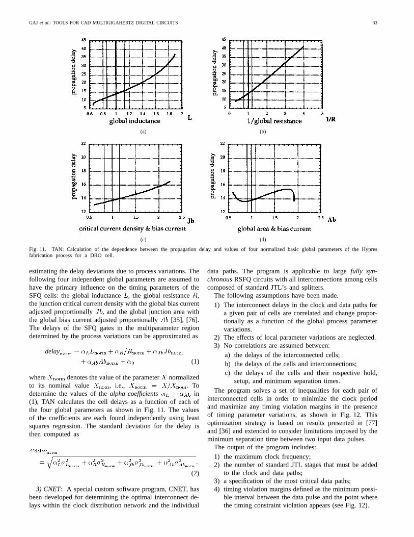
Fig. 11. TAN: Calculation of the dependence between the propagation delay and values of four normalized basic global parameters of the Hypresfabrication process for a DRO cell.
estimating the delay deviations due to process variations. Thefollowing four independent global parameters are assumed tohave the primary influence on the timing parameters of theSFQ cells: the global inductance, the global resistance ,the junction critical current density with the global bias currentadjusted proportionally , and the global junction area withthe global bias current adjusted proportionally [35], [76].The delays of the SFQ gates in the multiparameter regiondetermined by the process variations can be approximated as
delay
(1)
where denotes the value of the parameternormalizedto its nominal value , i.e., . Todetermine the values of thealpha coefficients in(1), TAN calculates the cell delays as a function of each ofthe four global parameters as shown in Fig. 11. The valuesof the coefficients are each found independently using leastsquares regression. The standard deviation for the delay isthen computed as
(2)
3) CNET: A special custom software program, CNET, hasbeen developed for determining the optimal interconnect de-lays within the clock distribution network and the individual
data paths. The program is applicable to largefully syn-chronousRSFQ circuits with all interconnections among cellscomposed of standard JTL’s and splitters.
The following assumptions have been made.
1) The interconnect delays in the clock and data paths fora given pair of cells are correlated and change propor-tionally as a function of the global process parametervariations.
2) The effects of local parameter variations are neglected.3) No correlations are assumed between:
a) the delays of the interconnected cells;b) the delays of the cells and interconnections;c) the delays of the cells and their respective hold,
setup, and minimum separation times.
The program solves a set of inequalities for each pair ofinterconnected cells in order to minimize the clock periodand maximize any timing violation margins in the presenceof timing parameter variations, as shown in Fig. 12. Thisoptimization strategy is based on results presented in [77]and [36] and extended to consider limitations imposed by theminimum separation time between two input data pulses.
The output of the program includes:
1) the maximum clock frequency;2) the number of standard JTL stages that must be added
to the clock and data paths;3) a specification of the most critical data paths;4) timing violation margins defined as the minimum possi-
ble interval between the data pulse and the point wherethe timing constraint violation appears (see Fig. 12).

34 IEEE TRANSACTIONS ON APPLIED SUPERCONDUCTIVITY, VOL. 9, NO. 1, MARCH 1999
TABLE VISURVEY OF BASIC TOOLSETS USED BY THE ACADEMIC AND INDUSTRIAL SDE RESEARCH GROUPS
Fig. 12. CNET: Definition of the timing violation margins in the presenceof variations in the fabrication process.
All outputs are obtained under the assumption that the timingparameters in the circuit remain within a 3range from theirnominal values.
H. Toolsets
Due to the increasing complexity of RSFQ circuits, it hasbecome clear that an integrated design environment is neededto assure adequate efficiency of the design process. Severalsuch environments are presented in Table VI.
The most complete integrated design environments arebased on the following tools for layout editing and circuitsimulation:
1) Cadence and Jspice3;2) Cadence and PSCAN;3) Xic and WRSpice.
The first environment has been calibrated at the Universityof Rochester and independently at TRW. The second designenvironment has been developed at SUNY Stony Brook,and the third environment has been developed by WhiteleyResearch, Inc. and adopted by Hypres, Inc. and Northrop-Grumman.
IV. FUTURE TOOLS
Existing RSFQ CAD tools permit the development of small–to medium-scale circuits but do not offer any support for thedesign of large-scale and very large-scale circuits.
The following more advanced CAD tools remain to bedeveloped.
A. Timing Optimizer
A timing optimizeris necessary to permit the interconnectdelays in the clock and the data paths of a large circuitto be optimally determined. The optimum clock schedulingprocedure is particularly complicated because active com-ponents such as Josephson Transmission Lines (JTL’s) areused to implement interconnect delays. The delays of theseinterconnects are comparable in magnitude to the delays oflogic gates. A timing optimizer must also consider a varietyof clocking schemes and clock distribution network topolo-gies developed specifically for RSFQ logic [36], [78]–[80].Additional challenges for timing in the RSFQ technologyinclude exceptionally high operating frequency and relativelylarge manufacturing induced parameter variations. The betaversion of such an optimizer, called CNET, with limitedcapabilities and applicable to synchronous circuits only, hasbeen developed at the University of Rochester and is describedin Section III-G3.
B. Automated Logic Synthesizer
An automated logic synthesizerneeds to be developedspecifically for RSFQ logic, in order to deal with the com-pletely different suite of basic gates, which does not includeelementary combinational gates (all RSFQ gates are clocked).The synthesis process would preferably include the clocksignal distribution. Additionally, the complexity of basic gates

GAJ et al.: TOOLS FOR CAD MULTIGIGAHERTZ DIGITAL CIRCUITS 35
differ in RSFQ technology; therefore, some gates may bepreferred over others, according to criteria which differ fromsemiconductor logic.
C. Automated Layout Synthesizer
The development of anautomated layout synthesizerforRSFQ logic is particularly challenging, in light of the useof active components for interconnects. Such interconnectshave large delays and occupy a significant area on the chip.Therefore, any straightforward placement and routing schemeis likely to lead to multiple violations of timing constraints. Asa result, a layout synthesizer for RSFQ logic must be integratedwith the timing optimizer, and both invoked iteratively until anear optimum solution is determined.
Without the development of these prospective tools, itis difficult to imagine further progress toward very large-scale RSFQ technology, particularly its application to generalpurpose computing.
V. TRENDS IN THE DEVELOPMENT
AND USE OF SDE CAD TOOLS
Presently, no consensus exists regarding which particularSDE CAD tool is preferable at any stage of the design process.Certain features of existing tools often complement each other.An experience with using a certain tool and the time necessaryto learn a new tool often outweigh advantages of switching toa new more advanced tool. As a result, even within the samecompany or university group, two or more tools of the samekind are used simultaneously by various designers and evenby the same person. No strong attempt to standardize toolswithin the same institution has been observed.
The use of various tools may be advantageous in terms ofexposing the designer to new experiences. However, it alsohas the disadvantage of making it more difficult to exchangedesigns when a close cooperation among designers from thesame or cooperating institutions is required. This effect may bereduced bystandardizing data formats. If the same standarddata format can be used to store the information describingthe circuit at each stage of the design process, then the datamay be more easily exported from one tool and imported toanother tool.
The following standard formats have been developed tofacilitate the exchange of data among varioussemiconductorCAD tools:
• CIF (CalTech Intermediate Form) [81], [82] and GDS II(Calma GDS II Stream Format) [82] at the layout level;
• EDIF at the schematic level [55];• Verilog HDL and VHDL at the behavioral level [67], [68].
The vast majority of existing layout tools used for the designof superconducting circuits support both CIF and GDSII.Tools for logic level simulation, adapted for RSFQ logic,such as Verilog XL, Leapfrog VHDL, Veriwell, and Eldo,also allow the transfer of behavioral models. Unfortunately,most schematic editors in use today do not support the reliableexport and import of schematics using EDIF. The authors hopethat this capability will be included in the new versions ofschematic editors.
New trends can be observed in the development of circuitsimulators. First, new types of analyzes targeted at supportingthe design of superconducting digital and mixed-signal circuitshave recently become available. These include Monte Carloanalysis, noise simulation [42], [43], error-rate simulation[83], and circuit animation [46]. Capabilities for mixed-modesimulation are being added to support the design of largedigital and mixed-signal circuits. More circuit simulators willbecome closely integrated with the timing optimizers despitethese optimizers being initially developed as stand-alone tools.
Together with the growing importance of logic simulation, ithas become necessary to extract information about the timingparameters included in the behavioral models of the gates. Inthe authors’ opinion, this function of timing analyzers (such asTAN) will need to be incorporated into the circuit simulators.
Further progress in optimization algorithms and their adap-tation to superconducting digital circuits can be expected. Itis likely that in the future, the figures of merit used duringoptimization will be extended to include both maximum circuityield and optimum timing parameters. This will allow themaximum intrinsic speed of a gate to be achieved once thegate is optimized.
Although sophisticated tools for layout editing and veri-fication of semiconductor circuits have been calibrated forsuperconducting electronics, the price limits their use to uni-versities (which benefit from substantial educational discounts)and large companies. The authors expect that inexpensivetools targeted at superconducting electronics will becomeavailable and widespread among small-sized and medium-sized companies. These tools will possess most of the featuresof their expensive counterparts, including reliable extractionof connectivity and all component values and full LVS ver-ification.
Accurate and fast inductance extractors are yet to be de-veloped. These tools need to use a standard layout viewof the circuit, either CIF or GDSII, as an input format.These tools should also combine the speed of existing 2-Dinductance extractors while providing the accuracy of existing3-D inductance estimators.
Finally, complete integrated design environments, with astraightforward design flow, supporting coherent and transfer-able design information and simplifying the use of standardcell libraries remain to be developed.
ACKNOWLEDGMENT
The authors would like to thank all participants of the SDECAD tools survey, in particular, S. Whiteley, P. Dresselhaus,D. Zinoviev, S. Polonsky, S. Kaplunenko, M. Jeffery, Z. Du,R. Koch, M. Biehl, H. Toepfer, J. Satchell, and P. Shevchenko,who shared with the authors their knowledge and experiencesregarding various tools they have developed, calibrated, orworked with. The authors appreciate the help and feedbackthey received from all participants of the working group onSDE CAD tools during the Workshop on SuperconductiveElectronics: Devices, Circuits & Systems in Winter Park,CO in September 1997. The authors are also grateful forvaluable comments to the manuscript from Prof. K. Likharev,
36 IEEE TRANSACTIONS ON APPLIED SUPERCONDUCTIVITY, VOL. 9, NO. 1, MARCH 1999
H. Toepfer, and T. Harnisch. Special thanks belong also to ourcollaborators A. Herr, N. Vukovic, D. Brock, C.-H. Cheah, B.Guan, C. Mancini, and P. Rott, who participated in the designof the Rochester SDE CAD tools, devoted their time to debugthese tools, used these tools for the first time, and gave theauthors the feedback necessary to improve the capabilities ofthe Rochester SDE design environment.
REFERENCES
[1] K. K. Likharev, “Ultrafast superconductor digital electronics: RSFQtechnology roadmap,”Czechoslovak J. Phys., Suppl. S6, vol. 46, 1996.
[2] K. K. Likharev, “Superconductors speed up computation,”Phys. World,pp. 39–43, May 1997.
[3] K. Gaj et al., “Toward a systematic design methodology for largemulti-gigahertz rapid single flux quantum circuits,”IEEE Trans. Appl.Superconduct., to be published.
[4] M. Aoyagi et al., “Chip layout design of a Josephson LSI circuit forexamining high-speed operability by using a standard cell automaticplacement and routing technique,”IEEE Trans. Appl. Superconduct.,vol. 4, pp. 169–176, Sept. 1994.
[5] M. Khalaf, S. Whiteley, and T. Van Duzer, “A computer-aided designframework for superconductor circuits,”IEEE Trans. Appl. Supercon-duct., vol. 5, pp. 3341–3344, June 1995.
[6] K. K. Likharev and V. K. Semenov, “RSFQ logic/memory family: Anew Josephson-junction technology for sub-terahertz-clock frequencydigital systems,”IEEE Trans. Appl. Superconduct., vol. 1, pp. 3–28,1991.
[7] K. K. Likharev, “Rapid single-flux-quantum logic,” inThe New Super-conductor Electronics, H. Weinstock and R. Ralston, Eds. Dordrecht:Kluwer, 1993, pp. 423–452.
[8] S. V. Polonskyet al., “New RSFQ circuits,”IEEE Trans. Appl. Super-conduct., vol. 3, pp. 2566–2577, 1993.
[9] S. V. Polonsky, V. K. Semenov, and A. F. Kirichenko, “Single flux,quantum B flip-flop and its possible applications,”IEEE Trans. Appl.Superconduct., vol. 4, pp. 9–18, 1994.
[10] V. K. Semenov, Yu. Polyakov, and D. Schneider, “Preliminary results onthe analog-to-digital converter based on RSFQ logic,” inCPEM Conf.Dig. Suppl., Braunschweig, Germany, June 1996, pp. 15–16.
[11] O. A. Mukhanov, P. D. Bradley, S. B. Kaplan, S. V. Rylov, and A. F.Kirichenko, “Design and operation of RSFQ circuits for digital signalprocessing,” inProc. 5th Int. Superconductivity Electron. Conf., Nagoya,Japan, Sept. 1995, pp. 27–30.
[12] Q. P. Herret al., “Design and low speed testing of a four-bit RSFQmultiplier-accumulator,”IEEE Trans. Appl. Superconduct., vol. 7, pp.3168–3171, 1997.
[13] O. A. Mukhanov, “RSFQ 1024-bit shift register for acquisition mem-ory,” IEEE Trans. Appl. Superconduct., vol. 3, pp. 3102–3113, Dec.1993.
[14] A. M. Herr, C. A. Mancini, N. Vukovic, M. F. Bocko, and M. J.Feldman, “High-speed operation of a 64-bit circular shift register,”IEEETrans. Appl. Superconduct., vol. 8, pp. 120–124, Sept. 1998.
[15] S. R. Whiteley, “Josephson junctions in SPICE3,”IEEE Trans. Mag.,vol. 27, no. 2, pp. 2902–2905, Mar. 1991.
[16] S. V. Polonsky, V. K. Semenov, and P. N. Shevchenko, “PSCAN:Personal superconductor circuit analyzer,”Superconduct. Sci. Technol.,vol. 4, pp. 667–670, 1991.
[17] Q. P. Herr and M. J. Feldman, “Multiparameter optimization of RSFQcircuits using the method of inscribed hyperspheres,”IEEE Trans. Appl.Superconduct., vol. 5, pp. 3337–3340, June 1995.
[18] P. I. Bunyk and S. V. Rylov, “Automated calculation of mutualinductance matrices of multilayer superconductor integrated circuits,”Ext. Abs. ISEC, p. 62, 1993.
[19] A. Krasniewski, “Logic simulation of RSFQ circuits,”IEEE Trans. Appl.Superconduct., vol. 3, pp. 33–38, Mar. 1993.
[20] K. Gaj, C.-H. Cheah, E. G. Friedman, and M. J. Feldman, “Functionalmodeling of RSFQ circuits using Verilog HDL,”IEEE Trans. Appl.Superconduct., vol. 7, pp. 3151–3154, June 1997.
[21] V. Adler, K. Gaj, D. K. Brock, C.-H. Cheah, and E. G. Friedman, “ACadence-based design environment for single flux quantum circuits,”IEEE Trans. Appl. Superconduct., vol. 7, pp. 3294–3297, June 1997.
[22] H. Toepfer, T. Harnisch, J. Kunert, S. Lange, and H. F. Uhlmann,“Formal description of the functional behavior of RSFQ logic circuits
for design and optimization purposes,”IEEE Trans. Appl. Superconduct.,vol. 7, pp. 3630–3633, June 1997.
[23] S. Polonsky, P. Shevchenko, A. Kirichenko, D. Zinoviev, and A.Rylyakov, “PSCAN’96: New software for simulation and optimizationof complex RSFQ circuits,”IEEE Trans. Appl. Superconduct., vol. 7,pp. 2685–2689, June 1997.
[24] V. K. Semenov, Y. A. Polyakov, and D. Schneider, “Implementationof oversampling analog-to-digital converter based on RSFQ logic,”Ext.Abs. ISEC, pp. 41–43, 1997.
[25] Proc. HTMT Project Meeting, Univ. Delaware, July 21, 1997.[26] Hybrid Technology Multithreaded Architecture Project Web Page. Avail-
able at http://www.cacr.caltech.edu/HTMT.[27] D. L. Miller, J. X. Przybysz, A. H. Worsham, and A. H. Miklich,
“Superconducting sigma-delta analog-to-digital converters,”Ext. Abs.ISEC, pp. 38–40, 1997.
[28] O. A. Mukhanov and S. V. Rylov, “Time-to-digital converters based onRSFQ digital counters,”IEEE Trans. Appl. Superconduct., vol. 7, pp.2669–2672, June 1997.
[29] A. F. Kirichenko, O. A. Mukhanov, and S. V. Rylov, “Superconductingtime-to-digital converters,”Ext. Abs. ISEC, pp. 34–37, 1997.
[30] V. K. Semenov, Y. A. Polyakov, and A. Ryzhikh, “Decimation filtersbased on RSFQ logic/memory cells,”Ext. Abs. ISEC, pp. 344–346, 1997.
[31] “Petaflops at SUNY stony brook,” web page. Available athttp://gamayun. physics.sunysb.edu/RSFQ/Research/PetaFLOPs.
[32] T. Sterling, P. Messina, and P. H. Smith,Enabling Technologies forPeta(FL)OPS Computing. Cambridge, MA: MIT, 1995.
[33] S. Whiteley,JSPICE3—User’s Manual.[34] Hypres Niobium Process Flow and Design Rules, Hypres, Inc., 175
Clearbrook Road, Elmsford, NY 10523 USA.[35] K. Gaj, Q. P. Herr, and M. J. Feldman, “Analysis of timing
requirements for basic RSFQ cells,” presented at theAppliedSuperconductivity Conf., Oct. 1994. Available http://www.ee.rochester.edu/users/sde/research/publications/asc94.
[36] K. Gaj, E. G. Friedman, and M. J. Feldman, “Timing of multi-gigahertzrapid single flux quantum digital circuits,”J. VLSI Signal Processing,vol. 9, pp. 247–276, 1997.
[37] K. Gaj, “Survey of SDE design tools.” Available on the web underhttp://www.ee.rochester.edu/users/sde/cad/survey.html.
[38] H. Toepfer, H. Uhlmann, M. Knoll, H. Thiele, and M. Selent, “Designtools for parameter determination and simulation of integrated Josephsonstructures,”IEEE Trans. Appl. Superconduct., vol. 5, pp. 3345–3348,1995.
[39] Odintsov, V. K. Semenov, and Zorin, “Specific problems of numericalanalysis of the Josephson junction circuits,”IEEE Trans. Mag., vol. 23,pp. 763–766, 1987.
[40] O. Mukhanov, V. K. Semenov, and K. K. Likharev, “Ultimate per-formance of the RSFQ logic circuits,”IEEE Trans. Mag., vol. 23, pp.759–762, 1987.
[41] M. Jeffery, private communication.[42] J. Satchell, “Stochastic simulation of SFQ logic,”IEEE Trans. Appl.
Superconduct., vol. 7, pp. 3315–3318, June 1997.[43] H. Toepfer, T. V. Filippov, and H. F. Uhlmann, “RSFQ cells: Transient
noise simulations,”Ext. Abs. ISEC, pp. 317–319, 1997.[44] D. K. Brock, private communication.[45] C. Hamilton and K. Gilbert, “Margins and yield in single flux quantum
logic,” IEEE Trans. Appl. Superconduct., vol. 1, pp. 157–163, Dec. 1991.[46] J. Satchell, private communication.[47] Q. P. Herr, “Bit errors and yield optimization in superconducting digital
single-flux-quantum electronics,” Ph.D. dissertation, Univ. Rochester,1997.
[48] Q. Herr and K. Gaj, MALT Reference Manual. Availablehttp://www.ee.rochester.edu/users/sde/research/software/malt/malt.refer-ence.guide.html.
[49] T. Harnisch and H. F. Uhlmann, “Application of different designcentering methods for yield optimization of cryoelectronic circuits,”Applied Superconductivity Inst. Phys. Conf., 1995, pp. 1717–1720.
[50] T. Harnisch, J. Kunert, H. Toepfer, and H. F. Uhlmann, “Designcentering methods for yield optimization of cryoelectronic circuits,”IEEE Trans. Appl. Supercond., vol. 7, pp. 3434–3437, June 1997.
[51] R. Koch and W. Benzing, “Multi-dimensional parameter optimizationfor RSFQ circuit design,”Ext. Abs. ISEC, pp. 305–307, 1997.
[52] S. Director and G. Hachtel, “The simplicial approximation approach todesign centering,”IEEE Trans. Circ. Syst., vol. 27, pp. 363–372, July1977.

GAJ et al.: TOOLS FOR CAD MULTIGIGAHERTZ DIGITAL CIRCUITS 37
[53] S. Director, W. Maly, and A. Strojwas,VLSI Design for Manufacturing:Yield Enhancement. Boston, MA: Kluwer, 1990.
[54] A. V. Rylyakov and S. V. Polonsky, “All-digital 1-bit RSFQ autocorrela-tor for radioastronomy applications: Design and experimental results,”IEEE Trans. Appl. Superconduct., Appendix, vol. 8, pp. 14–19, Mar.1998.
[55] EDIF WWW Home Page at http://www.edif.org/index.html.[56] W. H. Chang, “The inductance of a superconducting strip transmission
line,” J. Appl. Phys., vol. 50, no. 12, pp. 8129–8134, Dec. 1979.[57] M. J. Feldman, “Inductance calculation Rodeo, 1996–1997.” Available
on the web at http://www.ee.rochester.edu/users/sde/research/projects/Inductance/survey.html.
[58] B. Guan, M. J. Wengler, P. Rott, and M. J. Feldman, “Inductanceestimation for complicated superconducting thin film structures witha finite segment method,”IEEE Trans. Appl. Superconduct., vol. 7, pp.2776–2779, June 1997.
[59] A. R. Kerr, “Surface impedance of superconductors and normal con-ductors in EM simulators,”Electronics Division Internal Rep. no. 302,National Radio Astronomy Observatory, Charlottesville, VA, Feb. 19,1996.
[60] Z. Du, S. R. Whiteley, and T. Van Duzer, “Inductance calculation of3D superconducting structures,”Ext. Abs. ISEC, pp. 293–295, 1997.
[61] P. H. Xiao, E. Charbon, A. Sangiovanni-Vincentell, T. Van Duzer, andS. R. Whiteley, “INDEX: An inductor extractor for superconductingcircuits,” IEEE Trans. Appl. Superconduct., vol. 3, pp. 2629–2632, Mar.1993.
[62] G. Hildebrandt and F. H. Uhlmann, “Inductance calculation for inte-grated superconducting structures by minimizing free energy,”IEEETrans. Appl. Superconduct., vol. 5, pp. 2766–2769, June 1995.
[63] T. Nakazato and Y. Okabe, “Inductance computation of microscopicsuperconducting loop,”IEEE Trans. Appl. Superconduct., vol. 7, pp.3626–3629, June 1997.
[64] M. M. Khapaev, “Extraction of inductances of a multi-superconductortransmission line,”Superconduct. Sci. Technol., vol. 9, pp. 729–733,1996.
[65] , “Extraction of inductances of plane thin film superconductingcircuits,” Superconduct. Sci. Technol., vol. 10, pp. 389–394, 1997.
[66] P. Bunyk, A. Y. Kidiyarova-Shevchenko, and P. Litskevitch, “RSFQmicroprocessor: New design approaches,”IEEE Trans. Appl. Supercon-duct., Appendix, vol. 7, pp. 2697–2704, June 1997.
[67] Standard 1076–1993,IEEE Standard VHDL Language Reference Man-ual, IEEE, 1994.
[68] IEEE 1364 Standard,Verilog Hardware Description Language ReferenceManual (LRM).
[69] D. Perry,VHDL. New York: McGraw-Hill, 1991.[70] S. Palnitkar,Verilog HDL—A Guide to Digital Design and Synthesis.
Englewood Cliffs, NJ: Prentice-Hall, 1996.[71] A. M. Dewey, Analysis and Design of Digital Systems with VHDL.
New York: PWS, 1997.[72] J. R. Armstrong,Chip-Level Modeling with VHDL. Englewood Cliffs,
NJ: Prentice-Hall, 1989.[73] U. Golze,VLSI Chip Design with the Hardware Description Language
VERILOG. New York: Springer-Verlag, 1996.[74] D. Pellerin and D. Taylor,VHDL Made Easy! Englewood Cliffs, NJ:
Prentice Hall, 1997.[75] P. Ashenden,The VHDL Cookbook. Available at ftp://bears.ucsb.edu/
pub/VHDL/comp.lang.vhdl.[76] K. Gaj, Q. P. Herr, and M. J. Feldman, “Parameter variations and syn-
chronization of RSFQ circuits,”Applied Superconductivity Conf., Insti-tute of Physics, Bristol, U.K., 1995, Conf. Series #148, pp. 1733–1736.
[77] K. Gaj, E. G. Friedman, M. J. Feldman, and A. Krasniewski, “Aclock distribution scheme for large RSFQ circuits,”IEEE Trans. Appl.Superconduct., vol. 5, pp. 3320–3324, 1995.
[78] K. Gaj, “Timing of large RSFQ circuits,” collection of slides available athttp://www.ee.rochester.edu/users/sde/research/projects/rsfq/timing/title.html.
[79] Z. J. Deng, N. Yoshikawa, S. R. Whiteley, and T. Van Duzer, “Data-driven self-timed RSFQ digital integrated circuit and system,”IEEETrans. Appl. Superconduct., vol. 7, 1997.
[80] P. Patra, S. Polonsky, and D. Fussel, “Delay insensitive logic forRSFQ superconductor technology,”III Int. Symp. Advanced Researchin Asynchronous Circuits and Systems, 1996, pp. 42–53.
[81] C. A. Mead and L. A. Conway,Introduction to VLSI Systems. Reading,MA: Addison-Wesley, 1987, p. 115.
[82] S. M. Rubin,Computer Aids for VLSI Design. Reading, MA, Addison-Wesley, 1987, p. 275.
[83] J. Satchell, “Margins and errors in SFQ circuits,”Ext. Abs. ISEC, pp.44–46, 1997.
Kris Gaj received the M.Sc. and Ph.D. degrees inelectrical and computer engineering from WarsawUniversity of Technology, Poland, in 1988 and1992, respectively.
In 1991 he was a Visiting Scholar at SimonFraser University in Vancouver, Canada, where heworked on analysis of various BIST techniquesfor VLSI digital circuits. From 1992 to 1993, heheaded a research team at Warsaw University ofTechnology developing an implementation of theInternet standard for secure electronic mail, Privacy
Enhanced Mail. From 1994 to 1998, he was with the Department of ElectricalEngineering at the University of Rochester, where he worked on logic level de-sign, design automation and timing analysis of superconducting digital circuits.In 1998, he joined George Mason University as an Assistant Professor. Hiscurrent research interests include CAD tools, testing, cryptography, computerarithmetic, and hardware/software co-design. He is the author of the book oncodebreaking.
Quentin P. Herr received the B.S. degree in physics from Case WesternReserve University in 1992 and the M.A. degree in physics and Ph.D. degreein electrical engineering from the University of Rochester.
His research interest at Rochester focused on single-flux-quantum electron-ics, including yield optimization, design for high-speed operation, and biterror-rate measurement of digital circuits. Since 1997, he has continued thisresearch interest as a member of the Superconductor Electronics Organization,TRW, Inc., located in Redondo Beach, CA.
Victor Adler received the B.S. degree in electrical engineering and the B.A.degree in computer science from Duke University, Durham, NC, in 1992,the M.S. degree in electrical engineering from the University of Rochester,Rochester, NY, in 1993, and the Ph.D. degree in electrical engineering at theUniversity of Rochester in 1998.
He was an IBM Watson Scholar and worked preprofessionally at IBMMicroelectronics, Burlington, VT, between 1988 and 1992 in the areas of finalmodule test, packaging, circuit macro development, and standard cell design.He has been a Teaching and Research Assistant at the University of Rochestersince 1993. In 1997, he worked on clock skew scheduling at Intel Corp.In 1998, he joined Sun Microsystems. His research interests include designtechniques for high-performance CMOS and superconductive technologies.
Andy Krasniewski (M’95-SM’91–F’96) received the M.S., Ph.D., and D.S.(Doctor of Science) degrees in electronic engineering from the WarsawUniversity of Technology, Poland, in 1974, 1983, and 1989, respectively.
Since 1974 he has been with the Warsaw University of Technology,where he is currently a Professor and Associate Dean at the Faculty ofElectronics and Information Technology. From 1990 to 1992, he was a VisitingAssociate Professor at the Department of Electrical Engineering, University ofRochester, Rochester, NY. His research interests include testing and design fortestability, fault-tolerant computing, and superconducting digital electronics.
Dr. Krasniewski is a member of the ACM, and a member of the AAUP.

38 IEEE TRANSACTIONS ON APPLIED SUPERCONDUCTIVITY, VOL. 9, NO. 1, MARCH 1999
Eby G. Friedman received the B.S. degree fromLafayette College in 1979 and the M.S. and Ph.D.degrees from the University of California, Irvine,in 1981 and 1989, respectively, all in electricalengineering.
From 1979 to 1991, he was with Hughes Air-craft Company, rising to the position of Managerof the Signal Processing Design and Test Depart-ment, responsible for the design and test of high-performance digital and analog IC’s. He has beenwith the Department of Electrical and Computer
Engineering at the University of Rochester since 1991, where he is aProfessor and the Director of the High Performance VLSI/IC Design andAnalysis Laboratory. His current research and teaching interests include highperformance microelectronic design and analysis with application to high-speed portable processors and low-power wireless communications. He is theauthor of more than 100 papers and book chapters and the editor of threebooks in the fields of high-speed and low-power CMOS design techniquesand the theory and application of synchronous clock distribution networks.
Dr. Friedman is a Member of the editorial board ofAnalog IntegratedCircuits and Signal Processing, a member of the CAS BoG, and a Memberof the technical program committee of a number of conferences. He was aMember of the editorial board of the IEEE TRANSACTIONS ON CIRCUITS AND
SYSTEMS II: A NALOG AND DIGITAL SIGNAL PROCESSING, Chair of the VLSISystems and Applications CAS Technical Committee, Chair of the ElectronDevices Chapter of the IEEE Rochester Section, Chair of the VLSI trackfor ’96 and ISCAS’97, Technical Co-Chair of the 1997 IEEE InternationalWorkshop on Clock Distribution Networks, Editor of several special issuesin a variety of journals, and a recipient of the Howard Hughes Masters andDoctoral Fellowships, an IBM University Research Award, an OutstandingIEEE Chapter Chairman Award, and a University of Rochester College ofEngineering Teaching Excellence Award.
Marc J. Feldman received the Ph.D. degree inphysics from the University of California, Berkeley,in 1975.
He worked at Chalmers University, Sweden, andat the NASA/Goddard Institute for Space Studies,New York City, in the development of supercon-ducting receivers for radio astronomy observatories.He joined the faculty of Electrical Engineeringat the University of Virginia in 1985, where hedeveloped a variety of superconducting diodes forreceiver applications. He is now Senior Scientist and
Professor of Electrical Engineering at the University of Rochester. His currentresearch activities are directed toward the development of ultra-high-speedlarge-scale digital circuits using superconducting single-flux-quantum logic.