tms320c674x/omap-l1xprocessor serial ata (sata ... - ti. · pdf fileserial ata (sata)...
TRANSCRIPT

TMS320C674x/OMAP-L1x ProcessorSerial ATA (SATA) Controller
User's Guide
Literature Number: SPRUGJ8C
March 2011

2 SPRUGJ8C–March 2011Submit Documentation Feedback
© 2011, Texas Instruments Incorporated

Preface ....................................................................................................................................... 71 Introduction ........................................................................................................................ 9
1.1 Purpose of the Peripheral .............................................................................................. 9
1.2 Features Supported ................................................................................................... 10
1.3 Features Not Supported .............................................................................................. 10
1.4 Functional Block Diagram ............................................................................................. 10
1.5 Terminology Used in this Document ................................................................................ 11
1.6 Industry Standard(s) Compliance .................................................................................... 12
2 Architecture ...................................................................................................................... 132.1 Clock Control ........................................................................................................... 13
2.2 Signal Description ...................................................................................................... 14
2.3 Pin Multiplexing ........................................................................................................ 14
2.4 Interfacing to Single and Multiple Devices .......................................................................... 14
2.5 DMA ..................................................................................................................... 15
2.6 Transport Layer ........................................................................................................ 15
2.7 Link Layer ............................................................................................................... 15
2.8 Phy ....................................................................................................................... 15
2.9 Reset .................................................................................................................... 16
2.10 Initialization ............................................................................................................. 16
2.11 Interrupt Support ....................................................................................................... 17
2.12 EDMA Event Support .................................................................................................. 18
2.13 Power Management ................................................................................................... 18
3 Use Cases ........................................................................................................................ 183.1 General Utilities: Structures and Subroutines Sample Program Uses .......................................... 19
3.2 Example on Initialization and Spinning Up Device ................................................................ 32
3.3 Example of DMA Write Transfer ..................................................................................... 34
3.4 Example of DMA Read Transfer ..................................................................................... 35
4 Registers .......................................................................................................................... 364.1 HBA Capabilities Register (CAP) .................................................................................... 38
4.2 Global HBA Control Register (GHC) ................................................................................ 39
4.3 Interrupt Status Register (IS) ......................................................................................... 40
4.4 Ports Implemented Register (PI) ..................................................................................... 41
4.5 AHCI Version Register (VS) .......................................................................................... 41
4.6 Command Completion Coalescing Control Register (CCC_CTL) ............................................... 42
4.7 Command Completion Coalescing Ports Register (CCC_PORTS) ............................................. 43
4.8 BIST Active FIS Register (BISTAFR) ............................................................................... 44
4.9 BIST Control Register (BISTCR) ..................................................................................... 45
4.10 BIST FIS Count Register (BISTFCTR) .............................................................................. 47
4.11 BIST Status Register (BISTSR) ...................................................................................... 47
4.12 BIST DWORD Error Count Register (BISTDECR) ................................................................ 48
4.13 BIST DWORD Error Count Register (TIMER1MS) ................................................................ 48
4.14 Global Parameter 1 Register (GPARAM1R) ....................................................................... 49
4.15 Global Parameter 2 Register (GPARAM2R) ....................................................................... 50
3SPRUGJ8C–March 2011 Table of ContentsSubmit Documentation Feedback
© 2011, Texas Instruments Incorporated

www.ti.com
4.16 Port Parameter Register (PPARAMR) .............................................................................. 51
4.17 Test Register (TESTR) ................................................................................................ 52
4.18 Version Register (VERSIONR) ....................................................................................... 53
4.19 ID Register (IDR) ....................................................................................................... 53
4.20 Port Command List Base Address Register (P0CLB) ............................................................ 54
4.21 Port FIS Base Address Register (P0FB) ............................................................................ 54
4.22 Port Interrupt Status Register (P0IS) ................................................................................ 55
4.23 Port Interrupt Enable Register (P0IE) ............................................................................... 57
4.24 Port Command Register (P0CMD) .................................................................................. 58
4.25 Port Task File Data Register (P0TFD) .............................................................................. 61
4.26 Port Signature Register (P0SIG) ..................................................................................... 61
4.27 Port Serial ATA Status (SStatus) Register (P0SSTS) ............................................................ 62
4.28 Port Serial ATA Control (SControl) Register (P0SCTL) .......................................................... 63
4.29 Port Serial ATA Error (SError) Register (P0SERR) ............................................................... 64
4.30 Port Serial ATA Active (SActive) Register (P0SACT) ............................................................. 66
4.31 Port Command Issue Register (P0CI) .............................................................................. 66
4.32 Port Serial ATA Notification Register (P0SNTF) ................................................................... 67
4.33 Port DMA Control Register (P0DMACR) ........................................................................... 68
4.34 Port PHY Control Register (P0PHYCR) ............................................................................ 70
4.35 Port PHY Status Register (P0PHYSR) .............................................................................. 74
Appendix A Revision History ...................................................................................................... 75
4 Contents SPRUGJ8C–March 2011Submit Documentation Feedback
© 2011, Texas Instruments Incorporated

www.ti.com
List of Figures
1 SATA Subsystem Functional Block Diagram .......................................................................... 10
2 SATA Core Block Diagram ............................................................................................... 11
3 HBA Capabilities Register (CAP)........................................................................................ 38
4 Global HBA Control Register (GHC) .................................................................................... 39
5 Interrupt Status Register (IS) ............................................................................................ 40
6 Ports Implemented Register (PI) ........................................................................................ 41
7 AHCI Version Register (VS) ............................................................................................. 41
8 Command Completion Coalescing Control Register (CCC_CTL)................................................... 42
9 Command Completion Coalescing Ports Register (CCC_PORTS)................................................. 43
10 BIST Active FIS Register (BISTAFR) ................................................................................... 44
11 BIST Control Register (BISTCR) ........................................................................................ 45
12 BIST FIS Count Register (BISTFCTR) ................................................................................. 47
13 BIST Status Register (BISTSR) ......................................................................................... 47
14 BIST DWORD Error Count Register (BISTDECR).................................................................... 48
15 BIST DWORD Error Count Register (TIMER1MS) ................................................................... 48
16 Global Parameter 1 Register (GPARAM1R) ........................................................................... 49
17 Global Parameter 2 Register (GPARAM2R) ........................................................................... 50
18 Port Parameter Register (PPARAMR) .................................................................................. 51
19 Test Register (TESTR) ................................................................................................... 52
20 Version Register (VERSIONR) .......................................................................................... 53
21 ID Register (IDR) .......................................................................................................... 53
22 Port Command List Base Address Register (P0CLB) ................................................................ 54
23 Port FIS Base Address Register (P0FB) ............................................................................... 54
24 Port Interrupt Status Register (P0IS) ................................................................................... 55
25 Port Interrupt Enable Register (P0IE)................................................................................... 57
26 Port Command Register (P0CMD) ...................................................................................... 58
27 Port Task File Data Register (P0TFD).................................................................................. 61
28 Port Signature Register (P0SIG) ........................................................................................ 61
29 Port Serial ATA Status Register (P0SSTS) ............................................................................ 62
30 Port Serial ATA Control Register (P0SCTL) ........................................................................... 63
31 Port Serial ATA Error Register (P0SERR) ............................................................................. 64
32 Port Serial ATA Active Register (P0SACT) ............................................................................ 66
33 Port Serial ATA Active (SActive) Register (P0SACT) ................................................................ 66
34 Port Serial ATA Notification Register (POSNTF)...................................................................... 67
35 Port DMA Control Register (P0DMACR) ............................................................................... 68
36 Port PHY Control Register (P0PHYCR) ................................................................................ 70
37 Port PHY Status Register (P0PHYSR) ................................................................................. 74
5SPRUGJ8C–March 2011 List of FiguresSubmit Documentation Feedback
© 2011, Texas Instruments Incorporated

www.ti.com
List of Tables
1 MPY Bit Field of P0PHYCR .............................................................................................. 13
2 Signal Descriptions ........................................................................................................ 14
3 SATASS Memory Summary ............................................................................................. 36
4 SATA Controller Registers ............................................................................................... 37
5 HBA Capabilities Register (CAP) Field Descriptions ................................................................. 38
6 Global HBA Control Register (GHC) Field Descriptions.............................................................. 39
7 Interrupt Status Register (IS) Field Descriptions ...................................................................... 40
8 Ports Implemented Register (PI) Field Descriptions .................................................................. 41
9 AHCI Version Register (VS) Field Descriptions ....................................................................... 41
10 Command Completion Coalescing Control Register (CCC_CTL) Field Descriptions ............................ 42
11 Command Completion Coalescing Ports Register (CCC_PORTS) Field Description............................ 43
12 BIST Active FIS Register (BISTAFR) Field Descriptions............................................................. 44
13 BIST Control Register (BISTCR) Field Descriptions.................................................................. 45
14 BIST FIS Count Register (BISTFCTR) Field Description ............................................................ 47
15 BIST Status Register (BISTSR) Field Description .................................................................... 47
16 BIST DWORD Error Count Register (BISTDECR) Field Description............................................... 48
17 BIST DWORD Error Count Register (TIMER1MS) Field Description .............................................. 48
18 Global Parameter 1 Register (GPARAM1R) Field Descriptions..................................................... 49
19 Global Parameter 2 Register (GPARAM2R) Field Descriptions..................................................... 50
20 Port Parameter Register (PPARAMR) Field Descriptions ........................................................... 51
21 Test Register (TESTR) Field Descriptions ............................................................................. 52
22 Version Register (VERSIONR) Field Description ..................................................................... 53
23 ID Register (IDR) Field Description ..................................................................................... 53
24 Port Command List Base Address Register (P0CLB) Field Description ........................................... 54
25 Port FIS Base Address Register (P0FB) Field Description .......................................................... 54
26 Port Interrupt Status Register (P0IS) Field Descriptions ............................................................. 55
27 Port Interrupt Enable Register (P0IE) Field Descriptions ............................................................ 57
28 Port Command Register (P0CMD) Field Descriptions................................................................ 58
29 Port Task File Data Register (P0TFD) Field Descriptions ........................................................... 61
30 Port Signature Register (P0SIG) Field Description ................................................................... 61
31 Port Serial ATA Status Register (P0SSTS) Field Descriptions...................................................... 62
32 Port Serial ATA Control Register (P0SCTL) Field Descriptions..................................................... 63
33 Port Serial ATA Error Register (P0SERR) Field Descriptions ....................................................... 64
34 Port Serial ATA Active Register (P0SACT) Field Description ....................................................... 66
35 Port Serial ATA Active (SActive) Register (P0SACT) Field Description ........................................... 66
36 Port Serial ATA Notification Register (POSNTF) Field Description................................................. 67
37 Port DMA Control Register (P0DMACR) Field Description .......................................................... 68
38 Port PHY Control Register (P0PHYCR) Field Descriptions.......................................................... 70
39 Port PHY Status Register (P0PHYSR) Field Description ............................................................ 74
40 Document Revision History .............................................................................................. 75
6 List of Tables SPRUGJ8C–March 2011Submit Documentation Feedback
© 2011, Texas Instruments Incorporated

PrefaceSPRUGJ8C–March 2011
Read This First
About This Manual
This document describes the serial ATA (SATA) controller. The SATA controller is the successor of theparallel ATA/ATAPI controller that has served as the choice of the communication medium between aportable computer (PC) and a hard-disk drive for several decades.
Notational Conventions
This document uses the following conventions.
• Hexadecimal numbers are shown with the suffix h. For example, the following number is 40hexadecimal (decimal 64): 40h.
• Registers in this document are shown in figures and described in tables.
– Each register figure shows a rectangle divided into fields that represent the fields of the register.Each field is labeled with its bit name, its beginning and ending bit numbers above, and itsread/write properties below. A legend explains the notation used for the properties.
– Reserved bits in a register figure designate a bit that is used for future device expansion.
Related Documentation From Texas Instruments
The following documents describe the TMS320C674x Digital Signal Processors (DSPs) and OMAP-L1xApplications Processors. Copies of these documents are available on the Internet at www.ti.com. Tip:Enter the literature number in the search box provided at www.ti.com.
The current documentation that describes the DSP, related peripherals, and other technical collateral, isavailable in the C6000 DSP product folder at: www.ti.com/c6000.
SPRUGM5 — TMS320C6742 DSP System Reference Guide. Describes the C6742 DSP subsystem,system memory, device clocking, phase-locked loop controller (PLLC), power and sleep controller(PSC), power management, and system configuration module.
SPRUGM6 — TMS320C6746 DSP System Reference Guide. Describes the C6746 DSP subsystem,system memory, device clocking, phase-locked loop controller (PLLC), power and sleep controller(PSC), power management, and system configuration module.
SPRUGJ7 — TMS320C6748 DSP System Reference Guide. Describes the C6748 DSP subsystem,system memory, device clocking, phase-locked loop controller (PLLC), power and sleep controller(PSC), power management, and system configuration module.
SPRUGM7 — OMAP-L138 Applications Processor System Reference Guide. Describes theSystem-on-Chip (SoC) including the ARM subsystem, DSP subsystem, system memory, deviceclocking, phase-locked loop controller (PLLC), power and sleep controller (PSC), powermanagement, ARM interrupt controller (AINTC), and system configuration module.
SPRUFK9 — TMS320C674x/OMAP-L1x Processor Peripherals Overview Reference Guide. Providesan overview and briefly describes the peripherals available on the TMS320C674x Digital SignalProcessors (DSPs) and OMAP-L1x Applications Processors.
SPRUFK5 — TMS320C674x DSP Megamodule Reference Guide. Describes the TMS320C674x digitalsignal processor (DSP) megamodule. Included is a discussion on the internal direct memory access(IDMA) controller, the interrupt controller, the power-down controller, memory protection, bandwidthmanagement, and the memory and cache.
7SPRUGJ8C–March 2011 PrefaceSubmit Documentation Feedback
© 2011, Texas Instruments Incorporated

Related Documentation From Texas Instruments www.ti.com
SPRUFE8 — TMS320C674x DSP CPU and Instruction Set Reference Guide. Describes the CPUarchitecture, pipeline, instruction set, and interrupts for the TMS320C674x digital signal processors(DSPs). The C674x DSP is an enhancement of the C64x+ and C67x+ DSPs with addedfunctionality and an expanded instruction set.
SPRUG82 — TMS320C674x DSP Cache User's Guide. Explains the fundamentals of memory cachesand describes how the two-level cache-based internal memory architecture in the TMS320C674xdigital signal processor (DSP) can be efficiently used in DSP applications. Shows how to maintaincoherence with external memory, how to use DMA to reduce memory latencies, and how tooptimize your code to improve cache efficiency. The internal memory architecture in the C674xDSP is organized in a two-level hierarchy consisting of a dedicated program cache (L1P) and adedicated data cache (L1D) on the first level. Accesses by the CPU to the these first level cachescan complete without CPU pipeline stalls. If the data requested by the CPU is not contained incache, it is fetched from the next lower memory level, L2 or external memory.
8 Read This First SPRUGJ8C–March 2011Submit Documentation Feedback
© 2011, Texas Instruments Incorporated

User's GuideSPRUGJ8C–March 2011
Serial ATA (SATA) Controller
1 Introduction
During these times, the parallel ATA (PATA) interface has gone through changes to sustain the demandsof the newly emerging applications needs. However, the PATA controller reached a point where it requiredmajor changes to satisfy the upcoming applications requirements and this led to its successor, the birth ofthe SATA controller. This device has a built-in SATA controller with a single HBA port operating inAdvanced Host Controller Interface (AHCI) mode and is used to interface to data storage devices at both1.5 Gbits/second and 3.0 Gbits/second line speeds. AHCI describes a system memory structure thatcontains a generic area for control and status, and a table of entries describing a command list whereeach command list entry contains information necessary to program an SATA device, and a pointer to adescriptor table for transferring data between system memory and the device.
1.1 Purpose of the Peripheral
The SATA controller addresses the drawback of the PATA interface architecture, throughput, and protocolperspectives. PATA required 40/80 wire parallel cable with a length requirement not exceeding 18 inches.With the current hardware design, PATAs maximum transfer rate saturated to a 133 Mbytes/second oftransfer. In addition to newly added features, like Hot swapping and native command queuing, the SATAcontroller abandoned the parallel physical interface and transitioned to a serial format using two differentialpairs supporting up to 3 Mbits/second transfer rate, translating to a 300 Mbytes/second raw throughput.
With the intent on handling the previous and current role of the PATA controller and addressing the futureneeds, the SATA controller is architected with the option of operating in a Legacy mode, a mode thatbehaves similar to the PATA controller from the protocol/driver perspective, and a new AHCI mode that isdifferent from the Legacy mode allowing it to overcome the drawbacks of PATA as well as extendingPATAs capabilities. The SATA controller that is supported by this device supports AHCI mode of operationonly. AHCI is a PCI class device that acts as a data movement engine between system memory and serialATA devices. However, the AHCI controller on this device is integrated within the core chipset, a commonattribute for embedded devices. The AHCI controller supported has no support for Legacy mode ofoperation.
Communication between a device and software moves from the task file via byte-wide accesses to acommand FIS located in system memory that is fetched by the HBA. This reduces command setup timesignificantly, allowing for many more devices to be added to a single host controller. Software no longercommunicates directly to a device via the task file. In other words, all data transfers between the deviceand system memory occur through the HBA acting as a bus master to system memory. Whether thetransaction is of a DMA type or a PIO type (the use of the PIO command type is strongly discouraged andall transfers should be performed using DMA unless otherwise that a transaction is only performed via PIOcommand), the HBA fetches and stores data to memory, offloading the CPU. There is no accessible dataport. Software written for AHCI is not allowed to utilize any of the legacy mechanisms to program devices.
The SATA controller uses a less massive thinner flexible cable that can be up to 3 feet (1 meter) in lengthallowing for easier routing and better air ventilation inside a case. Its power budget is significantly reducedto 250 mV compared to the required 5V power of PATA.
Like its predecessor, the SATA controller is most commonly used by PCs and portable devices tointerface a host processor with data storage or CD/audio devices. It also has the support for hot swappingcapability. It also supports the use of a Port Multiplier to increase the number of devices that can beattached to the single HBA port.
9SPRUGJ8C–March 2011 Serial ATA (SATA) ControllerSubmit Documentation Feedback
© 2011, Texas Instruments Incorporated

R
x
T
x
Status
Synopsys SATA Core
TxFIFO
RxFIFO
*2AHB
AHB2*
PHY(SERDES)
Logic
Control
Introduction www.ti.com
1.2 Features Supported
The main features of the SATA controller are:
• Synopsis DWH Serial ATA 1.5 Gbps and 3 Gbps speeds core• Support for the AHCI controller spec 1.1• Integrated TI SERDES PHY• Integrated Rx and Tx data buffers• Supports all SATA power management features• Internal DMA engine per port• Hardware-assisted native command queuing (NCQ) for up to 32 entries• 32-bit addressing• Supports port multiplier with command-based switching• Activity LED support• Mechanical presence switch• Cold presence detect
1.3 Features Not Supported
Features not supported in this SATA controller are:
• Legacy mode of operation• Master/slave type of configuration• Far-end analog loopback• Message signaled interrupts• 64-bit addressing
1.4 Functional Block Diagram
The SATA subsystem (SATASS) is a fully contained serial ATA host with built-in DMA. It uses the AHCIstandard for communication with a SATA device. It has no support for the Legacy mode of operation.Figure 1 shows a high-level block diagram of the SATA subsystem (core and the integrated TI PHY).Figure 2 shows a high-level block diagram of the SATA core.
Figure 1. SATA Subsystem Functional Block Diagram
10 Serial ATA (SATA) Controller SPRUGJ8C–March 2011Submit Documentation Feedback
© 2011, Texas Instruments Incorporated

REGIF
PHYIF
DMAIF
PortBus
InterfaceUnit
BIUMaster
BIUSlave
PortDMA
PortRegisters
TransportLayer
LinkLayer
TxFIFO
Port Power Control Module
MasterIF
SlaveIF
PHYIF
RxFIFO
www.ti.com Introduction
Figure 2. SATA Core Block Diagram
1.5 Terminology Used in this Document
The following is a brief explanation of some terms used in this document:
Term MeaningAHCI Advanced host controller Interface (necessary for implementing newly supported
features like native command queuing). Freon device supports only this mode ofoperation, i.e., has no support for Legacy mode. It also reduces CPU/Softwareoverhead when moving data in and out of the system memory. Note that systemsoftware is responsible to ensure that queued and non-queued commands are notmixed in the command list.
ATA/ATAPI AT attachment/ATA packet interfaceCF Compact Flashdevice External SATA or ATAPI device attached to the SATA controllerDMA DMA within the ATA controller, not the processor EDMA systemDWORD DWORD is 32 bits of data.command list A memory buffer for as much as 32 commands. Each command is entered in a
command slot. This is a required feature when supporting command queuing.command slot A subset of the command list. It is the memory buffer for a single command. A total of
32 command slots exist.D2H Device to HBA. Mostly used to indicate the direction of the transmission of FIS that is
from device to the HBA (host).FIS Frame Information Structure. A frame is made of a data payload with computed CRC
and a start and end primitives.H2D HBA to device. Mostly used to indicate the direction of the transmission of FIS that is
from HBA (host) to device.HBA Host bus adapter. It is the SATA controller that implements the AHCI specification to
communicate between system memory and Serial ATA devices.Legacy mode This mode of operation makes the user access (application software or driver) to view
the SATA controller in a similar fashion as a PATA controller. This device does notsupport this mode of operation but AHCI mode of operation.
OOB Out of band. OOB signaling is used for during device detection and when recoveringfrom power states.
11SPRUGJ8C–March 2011 Serial ATA (SATA) ControllerSubmit Documentation Feedback
© 2011, Texas Instruments Incorporated

Introduction www.ti.com
Term MeaningPORT Refers to HBA port mainly, within this document. However, the PORT is also be used
to refer to a port of a PORT Multiplier.PRD Physical region descriptor. A PRD table is a data structure used by DMA engines that
comply with the ATA/ATAPI Host Adapters standard. The PRD describes memoryregions to be used as the source or destination of data during DMA transfers. A PRDtable is often referred to as a scatter/gather list.
PM Port Multiplier. A Port Multiplier allows extending an HBA port connection capability toconnect to multiple SATA devices, a maximum of 15 devices. Note that the operatingbandwidth is shared amongst all the Devices when using this type of configuration
SATA controller Serial ATA controller, also HBA.System memory The memory that is external from the SATA controller but is a memory that is
accessible by the built in SATA controller DMA or the CPU.
1.6 Industry Standard(s) Compliance
This module is compliant with the SATA revision 2.6 Gold standard and the AHCI revision 1.1specifications.
12 Serial ATA (SATA) Controller SPRUGJ8C–March 2011Submit Documentation Feedback
© 2011, Texas Instruments Incorporated

www.ti.com Architecture
2 Architecture
This section discusses the architecture of the Serial ATA Controller. The Serial ATA Controller supportsAdvanced Host Controller Interface (AHCI) operation only. It does not support the Legacy mode ofoperation. Since the controller complies with the AHCI standard (version 1.1) the details of its operation isdetailed within the AHCI version 1.1 specification. See the specification for the general behavior of theSATA Core operation. The SATA Controller supported within the Freon device has a single HBA port.
2.1 Clock Control
The SATA controller uses two internal clocks (SYSCLK2 and SYSCLK4) and one external differentialclock (REFCLKP/N) for its operation. SATA controller access to CPU and its resources is implementedthrough, SYSCLK2 (PLL0 output frequency divided by 2). SYCLK2 to the SATA controller is gated by thePSC and is required to be enabled prior to accessing the SATA controller. SYCLK4 (PLL0 outputfrequency divided by 4), is the keep alive clock and is always ON.
A high quality low jitter external differential clock is required as a source clock input for the PHY and thefrequency of the input clock should be between 75MHz and 375 MHz (depending upon the supportedmultiplier used). Maximum Jitter should not exceed 50ps pk-pk. Duty cycle must be between 40 and 60%.Nominal Rise/fall time should be 700 ps.
This input frequency requirement is dependent upon the supported PHY PLL multiplier value. The MPYfield of the port PHY control register (P0PHYCR) is programmed with the PLL multiplier value based onthe input frequency clock. Note that the PHY PLL output frequency should be exactly 1.5GHz (for both 3and 1.5 Gbits/Sec line rate) and its accuracy is very important to the operation of the SATA controller.
Table 1 shows the MPY bit field of P0PHYCR for supported PHY PLL multiplier values.
Table 1. MPY Bit Field of P0PHYCR
MPY Bit Field Value Effect
0 Reserved
1h 5×
2h 6×
3h Reserved
4h 8×
5h 10×
6h 12×
7h 12.5×
8h 15×
9h 20×
Ah 25×
Bh-Fh Reserved
13SPRUGJ8C–March 2011 Serial ATA (SATA) ControllerSubmit Documentation Feedback
© 2011, Texas Instruments Incorporated

Architecture www.ti.com
2.2 Signal Description
This device has bonded the Data lines (two sets of differential data lines) along the pins necessary fordetecting device insertion, power supply needs and powering a device. The power pins necessary topower up a cold SATA device should be handled external to the device, on the board along the signalpath connector.
Table 2. Signal Descriptions
Terminal Name Type Description
SATA_RXP Input SATA receive data (positive)
SATA_RXN Input SATA receive data (negative)
SATA_TXP Output SATA transmit data (positive)
SATA_TXN Output SATA transmit data (negative)
SATA_REFCLKP Input SATA PHY reference clock (positive)
SATA_REFCLKN Input SATA PHY reference clock (negative)
SATA_MP_SWITCH Input SATA mechanical presence switch input
SATA_CP_DET Input SATA cold presence detect input
SATA_CP_POD Output SATA cold presence power-on output
SATA_LED Output SATA LED control output
SATA_REG Output SATA PHY PLL regulator output. Requires an external 0.1 μF filter capacitor.
SATA_VDDR Power SATA PHY 1.8V internal regulator supply
SATA_VDD Power SATA PHY 1.2V logic supply
SATA_VSS Ground SATA PHY ground reference
2.3 Pin Multiplexing
Extensive pin multiplexing is used to accommodate the largest number of peripheral functions in thesmallest possible package. Pin multiplexing is controlled using a combination of hardware configuration atdevice reset and software programmable register settings. Refer to the device-specific data manual todetermine how pin multiplexing affects the SATA.
2.4 Interfacing to Single and Multiple Devices
The SATA Controller supports a single HBA port. This HBA port can be used to interface directly to asingle SATA device or to multiple SATA devices via a Port Multiplier. Note that on a multiple target setup,the available bandwidth will be shared amongst all the attached devices.
Note that Port Multipliers and Power Supplies for external SATA devices, when needed, should befurnished external to the device. However, the appropriate signals for controlling power and devicedetection are bonded and can be controlled via software.
2.4.1 Interfacing to a Single Device
If you need to interface directly to a single device, there is no need of populating a Port Multiplier. Thesoftware needs to ensure that the PMP field within the Command Header and the PM_PORT field of theFIS be cleared at all times.
If the external SATA device is not Self Powered, it is the responsibility of the System Designer to populateand furnish the right power supply needed. Consult the SATA specification for details.
2.4.2 Interfacing to Multiple Devices
Interfacing to multiple devices is similar to interfacing with a single device, except the existence of a PortMultiplier on the setup. The couple of additional tasks from the software perspective is that therequirement for the software to detect and configure the Port Multiplier prior and then after whenaccessing individual SATA devices, the software is required to populate the PMP filed of the CommandHeaders and PM_PORT field of the FISes with the Port Multiplier Port value.
14 Serial ATA (SATA) Controller SPRUGJ8C–March 2011Submit Documentation Feedback
© 2011, Texas Instruments Incorporated

www.ti.com Architecture
2.5 DMA
The HBA port contains two DMA engines: one to fetch commands from the command list and one to moveFISes in and out of system memory.
The DMA used to move FISes in and out of system memory has a port DMA control register (P0DMACR)to control the burst transfer. This DMA is used to transfer all information between system memory and theattached SATA device, as well as configuration and status FISes.
You can program the maximum burst size that is issued on the system bus independently for both readsand writes. The DMA issues transactions this size or smaller (in DWORD increments). This is used tooptimize burst size for overall system throughput efficiency. See Section 4.33 for details on valid values.Note that programming a burst size of greater than a transaction size, while not invalid, is meaninglessbecause the DMA maximizes out at transaction size.
You can also program the transaction size for both receive and transmit (see Section 4.33). Thetransaction size is the minimum amount of data that the DMA works on. For example, if there is a FIScoming from the device to the host, the DMA does not begin transferring data into system memory untilthere is at least rx_transaction_size (RXTS) data in the receive FIFO. During transmit, the DMA readsdata from system memory in tx_transaction_size (TXTS) increments to put into the transmit FIFO. Notethat transactions may be broken up into multiple bursts based on burst size, crossing of a 1K boundary, orend-of-frame.
2.6 Transport Layer
The transport layer handles all of the transport layer functions of the SATA protocol. During reception, itreceives a FIS from the Link layer via the Rx FIFO, decodes the type, and routes it to the proper locationvia the port DMA. During transmission, it transfers a FIS constructed by the port DMA to the link layer viathe Tx FIFO. It also passes link layer errors and checks for transport layer errors to pass up to the system.
The transport layer also contains the Tx and Rx FIFOs. These FIFOs are used as asynchronous databuffers between the serial domain and the bus clock domain. The size of these FIFOs affects thesubsystems ability to buffer data before flow control must be asserted. It also affects the maximumprogrammable transaction and burst sizes that can be programmed into the port DMA. The Tx FIFO sizeis 32 DWORDS (124 bytes) deep and the Rx FIFO size is 64 DWORDS (256 bytes) deep.
2.7 Link Layer
The link layer maintains the link and supports all SATA link layer functionality including:
• Out-of-band (OOB) transmit signaling• Frame negotiation and arbitration• Envelope framing/de-framing• CRC calculation (receive and transmit)• 8b/10b encoding/decoding• Flow control• Frame acknowledgment and status• Data width conversion• Data scrambling/descrambling• Primitive transmission• Primitive detection and dropping• Power management
2.8 Phy
The SATASS includes an integrated TI SERDES macro as a phy. The phy handles all of theserialization/de-serialization, symbol alignment, and Rx OOB signal detection. There is some logicbetween the Synopsis core and the SERDES for control and configuration.
15SPRUGJ8C–March 2011 Serial ATA (SATA) ControllerSubmit Documentation Feedback
© 2011, Texas Instruments Incorporated

Architecture www.ti.com
2.9 Reset
SATA peripheral reset is handled using the power and sleep controller (PSC). For detailed information onpower management procedures using the PSC, see your device-specific System Reference Guide. Othertypes of resets supported by the SATA controller are part of the AHCI specification is discussed within theAHCI specification 1.1. See the standard specification for the details on HBA reset, port rest and softwarereset.
2.10 Initialization
Proper initialization of the HBA is required after power-up to ensure proper operation of the SATAcontroller peripheral. The initialization process starts by performing a write to one-time write-only registers,this is documented as firmware initialization within the AHCI specification, where the values writtendepends on the features that the applications supports followed by software initialization. This part of theinitialization is similar to what a PC BIOS does and allows you to enable/disable some features bysoftware.
The software can then continue with a normal initialization that is required by the software and the detailsand sequence of initialization done here is also documented within the AHCI specification. In general, allresources that are required by the AHCI controller, PHY initialization, structures and memories forCommand Slots, FIS, and Data Memories are configured and the FIS DMAs is enabled. The software willthen spin-up the device and ensure that a proper Device Detection and Speed Negotiation has completedprior to enabling the Command DMA.
Note that DMA Configuration/Initialization should take place after Device Detection and SpeedNegotiation. If done earlier, the default value is used (this is the recommended setting) since RESETremoves the initialized value. The only time it is advisable to change the DMA Configuration is if you needto prioritize System Resource access. It also requires that the Command DMA is not running (P0CMD.ST= 0) when modifying the value of the DMA Configuration fields.
2.10.1 Initialization (Firmware and Software)
Software reads the HBA capabilities register (CAP), ports implemented register (PI), AHCI version register(VS), global parameter 1 register (GPARAM1R), global parameter 2 register (GPARAM2R), and the portparameter register (PPARAMR) to obtain information about the subsystems capabilities. The softwareshould then take the following steps to configure each port for operation:
1. Do all firmware capability writes.2. Setup all appropriate structures in memory as per the AHCI specification.3. Configure the PHY using the port PHY control register (P0PHYCR):
(a) Set the MPY bit field for the PLL multiply factor.(b) Set LOS = 1 (enable loss of signal detection)(c) Set ENPLL = 1 (enable the PLL)
4. Set the port command list base address register (P0CLB).5. Set the port FIS base address register (P0FB).6. Set appropriate bits in the port command register (P0CMD).7. Program the port serial ATA control register (P0SCTL).8. Wait for Device Detection and Speed Negotiation to end.9. Program the port DMA control register (P0DMACR).10. Enable the appropriate interrupts.11. Enable FIS reception in P0CMD.12. Spin-up the device(s), if necessary.
16 Serial ATA (SATA) Controller SPRUGJ8C–March 2011Submit Documentation Feedback
© 2011, Texas Instruments Incorporated

www.ti.com Architecture
2.10.2 Issuing a Command
Once the host and device are configured, perform the following steps to issue a command:
1. Create the appropriate FIS in system memory.2. Create the PRD.3. Queue the command to the command queue list (location specified by the port command list base
address register (P0CLB).
For detailed information, see the AHCI Specification Version 1.1.
2.11 Interrupt Support
The AHCI controller supports both standard interrupt sourcing, where interrupts are generated whenenabled events occur, or a different type method of generating interrupts that minimize interrupt loading byeither generating interrupts in a batch or periodically.
The interrupt handling method where interrupt loading issue is a factor is handled using CommandCompletion Coalescing method.
2.11.1 Command Completion Coalescing
Command Completion Coalescing (CCC) is a feature designed to reduce the interrupt and commandcompletion overhead in a heavily loaded system. The feature enables the number of interrupts taken percompletion to be reduced significantly, while ensuring a minimum quality of service for commandcompletions. When software specified number of commands have completed or a software specifiedtimeout has expired, an interrupt is generated by hardware to allow software to process completedcommands. the command completion coalescing ports register (CCC_PORTS) should be programmedwith 1 to indicate that the single available port, Port0, is selected.
For a detailed explanation of the CCC initialization and usage, see the AHCI Specification 1.1Section 11.6.
2.11.1.1 CCC Interrupt Based on Timer Expiration
When CCC is enabled and the desired method to receive an interrupt is based on a timer elapsecondition, then you need to communicate a resolution for a 1ms time by programming the BIST DWORDerror count register (TIMER1MS) with the VBUS cycle count derived from the VBUS clock frequencysourced to the SATA controller. For a DSP clock frequency of 300 MHz, the VBUS Clock is 150 MHz andthe 1ms cycle count is 150 MHz/1000 = 150000. This means that when the TV bit in the commandcompletion coalescing control register (CCC_CTL) is a non-zero value and the EN bit in CCC_CTL is setto 1 (CCC is enabled), it will take 15 ms or 15 × 150000 = 2,250,000 VBUS cycles for the timer to elapseand when it does, the CCC generates an interrupt. This happens periodically until disabled.
NOTE: Make sure the CC bit in the command completion coalescing control register (CCC_CTL) iscleared to 0.
2.11.1.2 CCC Interrupt Based on Completion Count
When CCC is enabled and the desired method to receive an interrupt is based on a completion count, thatis, the CC bit in the command completion coalescing control register (CCC_CTL) is programmed with anon-zero value and the CCC interrupt is enabled (EN bit in CCC_CTL is set to 1), an interrupt is sourcedfrom the SATA controller when the programmed desired number of interrupt is received.
NOTE: Make sure the TV bit in the command completion coalescing control register (CCC_CTL) iscleared to 0.
17SPRUGJ8C–March 2011 Serial ATA (SATA) ControllerSubmit Documentation Feedback
© 2011, Texas Instruments Incorporated

Use Cases www.ti.com
2.11.2 Non CCC Interrupt Configuration
For a standard interrupt handling method where every event that is enabled generates an interrupt, ishandled as follows. For more information, see the AHCI Specification.
After insuring that CCC is disabled, the EN bit in the command completion coalescing control register(CCC_CTL) is 0, in order for the SATA Core to source interrupts, the interrupt should be enabled at boththe global level (the IE bit in the global HBA control register (GHC) is 1) and at the port level by enablingthe bit fields for the desired interrupt. An enable bit at a Port level that control interrupts dispatch to theprocessor interrupt handling resource. So long as the CPU interrupt handler is configured properly, theCPU receives the interrupt when the enabled event occurs.
2.12 EDMA Event Support
The SATA controller makes use of its own built-in DMA and has no need nor utilizes the processor EDMA.
2.13 Power Management
The SATA controller can be placed in reduced power modes to conserve power during periods of no use.The main power management of the peripheral is controlled by the processor power and sleep controller(PSC). The PSC acts as a master controller for power management of all of the peripherals on theprocessor. For detailed information on power management procedures using the PSC, see yourdevice-specific System Reference Guide.
During times of the SATA peripheral use, the SATASS supports the industry standard power-down modes(both Partial and Slumber low-power modes) as provided within the SATA specification. These modesallow for power savings through powering down part of the SERDES PHY and the ability to gate off theclocks to the link layer. The Port Power Control Module is used to enter and exit these modes that mayhave the normal functional clocks gated off.
NOTE: When SATA communication is in the idle state, that is, when no disk activity takes place,the communication remains active with both the host and the device sending a logical syncprimitive and scrambled data at the speed negotiated continuously. For power sensitiveapplications, the power consumed during the disk inactivity stage might be undesirable and itmight be a desired task to place the communication interface into an electrical idle (Partial orSlumber) state until data transfer activity is needed in order to conserve power.
3 Use Cases
The following sections include some sample program snippets that can be used as a guide for softwaredevelopment. The example demonstrates one of the ways of creating the necessary structures; properlyaligned system memory resources, initialization, as well as performing basic DMA Read/Write transferusing Couple of Command Slots.
Section 3.1 contains examples in relations to System Memory resource allocations, Structures, andSubroutines used by the Initialization and Read/Write Transfer functions. The remaining sections includeexamples of basic Initialization, DMA Write transfer, and DMA Read transfer examples.
18 Serial ATA (SATA) Controller SPRUGJ8C–March 2011Submit Documentation Feedback
© 2011, Texas Instruments Incorporated

www.ti.com Use Cases
3.1 General Utilities: Structures and Subroutines Sample Program Uses/* Allocating memory for Command List. The structure pointed to by this
address range is 1K-bytes in length and must be 1K-byte aligned.Note that each command header occupies 32 bytes of memory and 32command headers require 1024 bytes of memory.
*/#pragma DATA_SECTION(CmdLists, ".L3_BUF");#pragma DATA_ALIGN(CmdLists, 1024);CmdListHeader CmdLists[32]={0};
/* Indicates the 32-bit physical address of the command table, whichcontains
the command FIS,ATAPI Command,andPRD table.
This address must be aligned to a 128-bytes of memory,*/#pragma DATA_SECTION(CmdTable, ".L3_BUF");#pragma DATA_ALIGN(CmdTable, 128);CommandTable CmdTable[LISTLENGTH];
/* Indicates the 32-bit base physical address for received FISes. Thestructure pointed to by this address range is 256 bytes in lengthand must be 256-byte aligned.
*/#pragma DATA_SECTION(RcvFis, ".L3_BUF");#pragma DATA_ALIGN(RcvFis, 256);ReceiveFis RcvFis;
#pragma DATA_SECTION(prdTableDataBuff, ".L3_BUF");unsigned char prdTableDataBuff[LISTLENGTH][PRDLENGTH][DATABUFFERLEN];
#define NUMOFPORTS (1) // Freon Supports A Single HBA Port. However it can support up to// 16 additional Ports with the use of an external Port Multiplier.// So keep this value to 1.
#define LISTLENGTH (2) // Max Command Header Per Port is 32
#define WRITE_CMD_SLOT (0) // Value used here should be <= LISTLENGTH-1#define READ_CMD_SLOT (1) // Value used here should be <= LISTLENGTH-1
// WARNING. PRDLENGTH can not be greater than 8 for this program.// See Note captured by the area when memory has been reserved for// within sata_utilities.c for Command Table "CmdTable" for// more information.
#if 1#define _MAX_DATA_TRANSFER_ // Define this in project file when needed.
#endif
#ifndef _MAX_DATA_TRANSFER_ // 512 Bytes Data Size within 2 PRD Descriptors.#define PRDLENGTH (2) // Max PRD Length is 65535 per port.#define DATABUFFERLEN (256) // DMA Data Buffer Length
#else // Max Data Size Transfer 8K Bytes within 2 PRD Descriptors#define PRDLENGTH (2) // Max PRD Length is 65535 per port.#define DATABUFFERLEN (2*4096) // DMA Data Buffer Length
#endif
#if ((PRDLENGTH > 8) | (WRITE_CMD_SLOT > LISTLENGTH-1) | (READ_CMD_SLT > LISTLENGTH-1))#error PRDLENGTH ENTRY ERROR - PROGRAM HARD CODED FOR MAX VALUE OF 8 - CMD SLOT ENTRY ERROR#endif
#define DESIRED_SPEED (GEN1) // GOASFASTASDEVICE, GEN1, GEN2#define DEVICE_LBA_ADDRESS (0x00000002) // Dev28bitLbaAddress = 28-Bit LBA Address#define WAIT_500_MILLISECONDS (50) // This should be set to 500 once the ONE_MS_VALUE isprogrammed correctly.#define WAIT_1_MILLISECOND (1)#define ONE_MS_VALUE (1) // Number of CPU Cycles needed to generate a millisecondwait time.#define DMA_BURST_LENGTH (0x9) // [0x0 - 0x9] Burst=2^(–1) i.e., 0x8=> 2^(9-1)=256#define DMA_TRANSACTION_SIZE (0x4) // [0x0 - 0xA] TransSize=2^n i.e., 0xA=> 2^10=1024
19SPRUGJ8C–March 2011 Serial ATA (SATA) ControllerSubmit Documentation Feedback
© 2011, Texas Instruments Incorporated

Use Cases www.ti.com
/////////////////////////////////////////////////////////////////////////////////////////////// Maximum of 32 commands slots per port exist where each command occupies 8 DWs (64 Bytes).// The structure 'CmdListHeader' defines a single command header definition.// The start of the first Command List &CmdListHeader[0] needs to be programmed onto P0CLB.//// Command List Base Address should be 1K Byte Aligned.
typedef struct {Uint32 CmdLen:5; //bits[4:0]Uint32 Atapi:1; //bit[5]Uint32 Write:1; //bit[6]Uint32 Prefetch:1; //bit[7]Uint32 Reset:1; //bit[8]Uint32 Bist:1; //bit[9]Uint32 Rok:1; //bit[10]Uint32 Rsv:1; //bit[11]Uint32 Pmp:4; //bits[15:12]Uint32 Prdtl:16; //bits[31:16]
}CmdListHeaderW0;
typedef struct {Uint32 PrdByteCnt; //bits[31:0]
}CmdListHeaderW1;
typedef struct {// Uint32 CmdTableAddLowRsv:7; //bit[6:0]// Uint32 CmdTableAddLow:25; //bits[31:7]
Uint32 CmdTableAddLow; //bits[31:7]}CmdListHeaderW2;
typedef struct {Uint32 CmdTableAddHigh; //bits[31:0]
}CmdListHeaderW3;
typedef struct {CmdListHeaderW0 DW0;CmdListHeaderW1 DW1;CmdListHeaderW2 DW2;CmdListHeaderW3 DW3;Uint32 DW4;Uint32 DW5;Uint32 DW6;Uint32 DW7;
} CmdListHeader;
typedef struct {Uint32 B0FisType:8;//bits[7:0]Uint32 BYTE1:8; //bits[15:8]Uint32 B2Cmd:8; //bits[23:16]Uint32 B3Feature:8;//bits[31:24]
}CmdFisWord0;
typedef struct {Uint32 B0LbaLow:8; //bits[7:0]Uint32 B1LbaMid:8; //bits[15:8]Uint32 B2LbaHigh:8;//bits[23:16]Uint32 B3Device:8; //bits[31:24]
}CmdFisWord1;
typedef struct {Uint32 B0LbaLowExp:8; //bits[7:0]Uint32 B1LbaMidExp:8; //bits[15:8]Uint32 B2LbaHighExp:8;//bits[23:16]Uint32 B3FeatureExp:8; //bits[31:24]
}CmdFisWord2;
typedef struct {Uint32 B0SecCnt:8; //bits[7:0]Uint32 B1SecCntExp:8; //bits[15:8]
20 Serial ATA (SATA) Controller SPRUGJ8C–March 2011Submit Documentation Feedback
© 2011, Texas Instruments Incorporated
www.ti.com Use Cases
Uint32 B2Rsv:8; //bits[23:16]Uint32 B3Control:8; //bits[31:24]
}CmdFisWord3;
typedef struct {Uint32 DWResv; //bits[31:0]
}CmdFisWord4;
typedef struct {CmdFisWord0 DW0;CmdFisWord1 DW1;CmdFisWord2 DW2;CmdFisWord3 DW3;CmdFisWord4 DW4;Uint32 DW5;Uint32 DW6;Uint32 DW7;Uint32 DW8;Uint32 DW9;Uint32 DW10;Uint32 DW11;Uint32 DW12;Uint32 DW13;Uint32 DW14;Uint32 DW15;
}CommandFIS;
//-----------Command FIS end ATAPI Command ------
// ATAPI Command Data Structuretypedef struct {
Uint32 ATAPI[4];}Atapi;
//-----------ATAPI Command end PRDT -------------// Physical Region Descriptor Table Data Structuretypedef struct {
Uint32 DbaLow; //bits[31:0]}DbaAddressLow;
typedef struct {Uint32 DbaHigh; //bits[31:0]
}DbaAddressHigh;
typedef struct {Uint32 DW2Reserved; //bits[31:0]
}PrdtRsv;
typedef struct {Uint32 DataBC:22; //bits[21:0]
}DataByteCnt;
typedef struct {DbaAddressLow DW0;DbaAddressHigh DW1;PrdtRsv DW2;DataByteCnt DW3;
}PRDT;//-----------PRDT end ---------------------------
//-----------Command Table Data Structure -------// Since Command Table has to be 128 bytes = 0x80 bytes aligned if supporting more// than a single Command Header, then need to make sure that the Array you are// creating for all associated Command Tables match the 128 bytes alignment.// In order to do so, the number of PRD Table length you are allocating should be// multiples of 8.typedef struct {
CommandFIS cfis;Atapi atapi;Uint32 Rsv[12];PRDT prdTable[16]; // Have forced this size to 8 in order to meet the minimum
// required size for Command Table.
21SPRUGJ8C–March 2011 Serial ATA (SATA) ControllerSubmit Documentation Feedback
© 2011, Texas Instruments Incorporated

Use Cases www.ti.com
}CommandTable;
//-----------Command Table Data Structure end ---
/////////////////////////////////////////////////////////////////////////////////////////////// Receive FIS requires the Receive FIS to be 256 byte aligned. P0FB should be programmed// with this restriction.//// RECEIVE FIS Data Structure// Members: DMA Setup FIS (DSFIS)// PIO Setup FIS (PSFIS)// D2H Register FIS (RFIS)// Set Device Bits FIS (SDBFIS)// Unknown FIS (UFIS)
//-----------DMA Setup FIS-----------------------
typedef struct {Uint32 B0FisType:8;//bits[7:0]Uint32 BYTE1:8; //bits[15:8]Uint32 B2Rsv:8; //bits[23:16]Uint32 B3Rsv:8; //bits[31:24]
}DsfisW0;
typedef struct {DsfisW0 DW0;Uint32 DW1DmaBuffLow;Uint32 DW2DmaBuffHigh;Uint32 DW3Rsv;Uint32 DW4DmaBuffOffset;Uint32 DW5DmaXfrCnt;Uint32 DW6Rsv;
}DMASetupFis;
//-----------DMA Setup FIS end PIO Setup FIS ----
typedef struct {Uint32 B0FisType:8;//bits[7:0]Uint32 BYTE1:8; //bits[15:8]Uint32 B2Status:8; //bits[23:16]Uint32 B3Errror:8;//bits[31:24]
}PioSetupDW0;
typedef struct {Uint32 B0LbaLow:8; //bits[7:0]Uint32 B1LbaMid:8; //bits[15:8]Uint32 B2LbaHigh:8;//bits[23:16]Uint32 B3Device:8; //bits[31:24]
}PioSetupDW1;
typedef struct {Uint32 B0LbaLowExp:8; //bits[7:0]Uint32 B1LbaMidExp:8; //bits[15:8]Uint32 B2LbaHighExp:8;//bits[23:16]Uint32 B3Rsv:8; //bits[31:24]
}PioSetupDW2;
typedef struct {Uint32 B0SecCnt:8; //bits[7:0]Uint32 B1SecCntExp:8; //bits[15:8]Uint32 B2Rsv:8; //bits[23:16]Uint32 B3Estatus:8; //bits[31:24]
}PioSetupDW3;
typedef struct {Uint32 HW0XferCnt:16; //bits[15:0]Uint32 HW1Rsv:16; //bits[31:16]
}PioSetupDW4;
22 Serial ATA (SATA) Controller SPRUGJ8C–March 2011Submit Documentation Feedback
© 2011, Texas Instruments Incorporated

www.ti.com Use Cases
typedef struct {PioSetupDW0 DW0;PioSetupDW1 DW1;PioSetupDW2 DW2;PioSetupDW3 DW3;PioSetupDW4 DW4;
}PIOSetupFis;
//-----------PIO Setup FIS end D2H Reg FIS-------
typedef struct {Uint32 B0FisType:8;//bits[7:0]Uint32 BYTE1:8; //bits[15:8]Uint32 B2Status:8; //bits[23:16]Uint32 B3Errror:8;//bits[31:24]
}D2HRegDW0;
typedef struct {Uint32 B0LbaLow:8; //bits[7:0]Uint32 B1LbaMid:8; //bits[15:8]Uint32 B2LbaHigh:8;//bits[23:16]Uint32 B3Device:8; //bits[31:24]
}D2HRegDW1;
typedef struct {Uint32 B0LbaLowExp:8; //bits[7:0]Uint32 B1LbaMidExp:8; //bits[15:8]Uint32 B2LbaHighExp:8;//bits[23:16]Uint32 B3Rsv:8; //bits[31:24]
}D2HRegDW2;
typedef struct {Uint32 B0SecCnt:8; //bits[7:0]Uint32 B1SecCntExp:8; //bits[15:8]Uint32 HW1Rsv:16; //bits[31:16]
}D2HRegDW3;
typedef struct {Uint32 W0Rsv; //bits[31:0]
}D2HRegDW4;
typedef struct {D2HRegDW0 DW0;D2HRegDW1 DW1;D2HRegDW2 DW2;D2HRegDW3 DW3;D2HRegDW4 DW4;
}D2HRegFis;
//-----------D2H Reg FIS end Set Device Bits FIS-// The Set Device Bit FIS definition does not contain the 2nd Word required// for Native Command Queueing. This second word is the SACTVE register and// the AHCI takes care of updating SACTIVE register at its location.
typedef struct {Uint32 B0FisType:8;//bits[7:0]Uint32 BYTE1:8; //bits[15:8]Uint32 B2Status:8; //bits[23:16]Uint32 B3Errror:8; //bits[31:24]
}SetDevBitsDW0;
typedef struct {Uint32 W1Rsv; //bits[31:0]
}SetDevBitsDW1;
typedef struct {SetDevBitsDW0 DW0;SetDevBitsDW1 DW1;
}SetDevBitsFis;
//-----------Set Device Bits FIS end Unkonwn FIS-
23SPRUGJ8C–March 2011 Serial ATA (SATA) ControllerSubmit Documentation Feedback
© 2011, Texas Instruments Incorporated

Use Cases www.ti.com
typedef struct {Uint32 UserDefined; //bits[31:0]
}UnknownDWx;
typedef struct {UnknownDWx DW[16]; // 16 Words (Max 64 Bytes allowed)
}UnknownFis;
//-----------Unkonw FIS end----------------------
//-----------Receive Register FIS Structure------
typedef struct {DMASetupFis DSFIS;Uint32 Rsv1;PIOSetupFis PSFIS;Uint32 Rsv2[3];D2HRegFis RFIS;Uint32 Rsv3;SetDevBitsFis SDBFIS;UnknownFis UFIS;
}ReceiveFis;
/
typedef struct {Uint8 cfisType;Uint8 cfisByte1;Uint8 cfisCmd;Uint8 cfisFeature;Uint8 cfisDw1SecNumLbaLow;Uint8 cfisDw1CylLowLbaMid;Uint8 cfisDw1CylHighLbahigh;Uint8 cfisDw1Dev;Uint8 cfisDw2SecNumLbaLowExp;Uint8 cfisDw2CylLowLbaMidExp;Uint8 cfisDw2CylHighLbahighExp;Uint8 cfisDw2FeatureExp;Uint8 cfisDw3SecCnt;Uint8 cfisDw3SecCntExp;Uint8 cfisDw3Ctrl;
}cmdFis;
typedef struct {Uint8 dsfisType;Uint8 dsfisByte1;Uint32 dsfisDw1DmaBuffLow;Uint32 dsfisDw2DmaBuffHigh;Uint32 dsfisDw4DmaBuffOffset;Uint32 dsfisDw5DmaXferCnt;
}dsFis;
typedef struct {Uint8 psfisType;Uint8 psfisByte1;Uint8 psfisStatus;Uint8 psfisError;Uint8 psfisDw1SecNumLbaLow;Uint8 psfisDw1CylLowLbaMid;Uint8 psfisDw1CylHighLbahigh;Uint8 psfisDw1Dev;Uint8 psfisDw3SecCnt;Uint8 psfisDw3Estatus;Uint16 psfisDw4XferCnt;
}piosFis;
typedef struct {Uint8 regfisType;Uint8 regfisByte1;
24 Serial ATA (SATA) Controller SPRUGJ8C–March 2011Submit Documentation Feedback
© 2011, Texas Instruments Incorporated

www.ti.com Use Cases
Uint8 regfisStatus;Uint8 regfisError;Uint8 regfisDw1SecNumLbaLow;Uint8 regfisDw1CylLowLbaMid;Uint8 regfisDw1CylHighLbahigh;Uint8 regfisDw1Dev;Uint8 regfisDw3SecCnt;
}regFis;
typedef struct {Uint8 sdbfisType;Uint8 sdbfisByte1;Uint8 sdbfisStatus;Uint8 sdbfisError;
}sdbFis;
typedef struct {Uint32 ufisWord[16];
}uFis;
typedef struct {Uint32 capSMPS:1;Uint32 capSSS:1;Uint32 piPi:2;Uint32 p0cmdCpd:1;Uint32 p0cmdEsp:1;Uint32 p0cmdMpsp:1;Uint32 p0cmdHpcp:1;Uint32 rsv:24;
}FirmwareCtrlFeatures;
void initMemory(Uint32 *startAddress, Uint32 length, Uint32 seedWord, Uint32 modifyVal) {Uint32 I;*startAddress++ = seedWord;for (I=0; i<length-1; I++) {
seedWord += modifyVal;*startAddress++ = seedWord;
}}
void clearCmdList(void) {//clear Host to Device (Command FIS) SpaceinitMemory((Uint32*)CmdLists, (LISTLENGTH*(sizeof(CmdListHeader)/4)), 0, 0);
}
void clearCmdTables(void) {Uint16 cmdSlot;for (cmdSlot=0; cmdSlot<LISTLENGTH; cmdSlot++) {
//Clear Command FIS and ATAPI Command Spaces for Command Header X; LISTLENGTH < X < 0initMemory((Uint32 *)&CmdTable[cmdSlot], (sizeof(CommandFIS)/4)+(sizeof(Atapi)/4), 0, 0);//Clear PRD Descriptor Locations for Command Header X; LISTLENGTH < X < 0initMemory((Uint32*)((Uint32)&CmdTable[cmdSlot]+0x80),
(sata_input_filePageSize*(sizeof(PRDT)/4)*sata_input_prdLength), 0, 0);}
}
void clearRcvFis() {//clear Receive DMA Setup FIS Space.initMemory((Uint32*)&RcvFis, (sizeof(DMASetupFis)/4), 0, 0);//clear Receive PIO Setup FIS Space.initMemory((Uint32*)((Uint32)&RcvFis+0x20), (sizeof(PIOSetupFis)/4), 0, 0);//clear Receive Device to Host (D2H) Register FIS Space.initMemory((Uint32*)((Uint32)&RcvFis+0x40), (sizeof(D2HRegFis)/4), 0, 0);//clear Set Device Bits FIS Space.initMemory((Uint32*)((Uint32)&RcvFis+0x58), (sizeof(SetDevBitsFis)/4), 0, 0);//clear Unknow FIS Space.initMemory((Uint32*)((Uint32)&RcvFis+0x60), (sizeof(UnknownFis)/4), 0, 0);
}
void clearDmaBuffers(void) {//Clear PRD Data Buffer Memory
25SPRUGJ8C–March 2011 Serial ATA (SATA) ControllerSubmit Documentation Feedback
© 2011, Texas Instruments Incorporated

Use Cases www.ti.com
initMemory((Uint32 *)prdTableDataBuff, (LISTLENGTH*PRDLENGTH*DATABUFFERLEN/4), 0, 0);}
void performFirmwareInit(void) {/* Firmware Initialization*/// Make sure you perform a Single Write in one operation of all HwInit Fields// initialization defined within a single register
sataRegs->CAP |= ((swCtrlFeatures.capSMPS << 28) |(swCtrlFeatures.capSSS << 27)
);// Configure PI[31:0]
sataRegs->PI |= (swCtrlFeatures.piPi << 0);
// Configure P0CMD[ESP,CPD,MPSP,HPCP=21,20,19,18]sataRegs->P0CMD |= ((swCtrlFeatures.p0cmdEsp << 21) |
(swCtrlFeatures.p0cmdCpd << 20) |(swCtrlFeatures.p0cmdMpsp << 19)|(swCtrlFeatures.p0cmdHpcp << 18)
);
/* Software Initialization*/// Initialize PHY and DMA Parameters (Corresponding to Gen1/2i timing)sataRegs->P0PHYCR = 0x80182048;
initBaseAddresses(); // Initialize Command List (P0CLB) and Receive FIS (P0FS)
// Configure Line Speed.setSataSpeed(DESIRED_SPEED); //GOASFASTASDEVICE=0,GEN1=1,GEN2=2
enableRcvFis(); // Enable Receive DMA
// The below are general Semaphores/Flags used and want to make sure they are initialized.// 28 Bit LBA Address of Device. 0xFFFFFFFF is used by test S/W to indicate that it is not
initializedDev28bitLbaAddress = 0xFFFFFFFF; // S/W needs to initialize this variable prior to calling
//_INT_DRIVEN_TEST_ is defined within the Project File#ifdef _INT_DRIVEN_TEST_
intHandlingMethod = USE_INT_HANDLER;#else
intHandlingMethod = USE_POLLING;#endif
}
char spinUpDeviceAndWaitForInitToComplete(void) {// Make sure that the HBA is in a Listen Mode prior to Spinning Up Device// Following Configuration is not allowed.// [P0SCTL.DET, P0CMD.SUD] = [1,1] NOT Allowed.if((sataRegs->P0SCTL & AHCI_PxSCTL_PxSSTS_DET) != 0)
sataRegs->P0SCTL &= ~(0xf << AHCI_PxSCTL_PxSSTS_DET_SHIFT);
// Clear P0SERR.DIAG.X (RWC bit field) so that the P0TFD is updated by HBA.sataRegs->P0SERR |= 0x04000000;
// Spin Up Device.sataRegs->P0CMD |= (1 << AHCI_PxCMD_SUD_SHIFT);
// Wait for Device Detection or/and Speed Negotiation to take place and finish.while ((sataRegs->P0SSTS & AHCI_PxSCTL_PxSSTS_DET) !=0x3);
// Device would send its status and and default Task file regs content (signature)// when finished with Power Up: Look for Device ready status.while ((sataRegs->P0TFD & AHCI_PxTFD_STS_BSY_DRQ_ERR) != 0);
// Make sure that the expected Device signature is received.if (sataRegs->P0SIG != AHCI_P0SIG_SIG_ATA_DEV_GOOD_STAT) // LBAhigh:LBAmid:LBAlow:SECcnt
return(1); // =0x00000101
return(0);
26 Serial ATA (SATA) Controller SPRUGJ8C–March 2011Submit Documentation Feedback
© 2011, Texas Instruments Incorporated

www.ti.com Use Cases
}
void initIntAndClearFlags(void) {// Make sure Interrupt is disabled (Disable at Port Level followed by Global Level).// Clear Interrupt at Port LevelenableDisableInt(PORTint, DISABLE, 0xFFFFFFFF); // clearInt(int type, intState, specificField)
// int type=GLOBALint or PORTint// intState=DISABLE or ENABLE// specificField=bit field to Enable or Disable// is used for the RWC feature for PORTint
// Disable interrrupt at Global LevelenableDisableInt(GLOBALint, DISABLE, 0); // clearInt(intType, intState fields2clr)
// int type=GLOBALint or PORTint// intState=DISABLE or ENABLE// fields2clr=dontcare for GLOBALint// is used for the RWC feature for PORTint
// Need to clear interrupts at Port Level followed by Global Level.// Ensure all pending Port Error and Status are cleared.clearIntOrErrorDiag(ERRORFIELDS, sataRegs->P0SERR); // Clear P0SERR Register// Ensure all pending Port Interrupts and The Single Global Interrupt are cleared.clearIntOrErrorDiag(INTFIELDS, sataRegs->P0IS); // Clear P0IS and IS Regs
}
void invokeHBAReset() {// HBA Reset will not affect the following Registers settings of PxFB and PxCLB// regs and HwInit fields of Port Registers are not affected.// To Do: Check if the Global Registers are affected. Spec mentions not affected.
// Note: COMRESET OOB will not be sent to attached Device because Freon supports// Staggered Spinup capability and P0CMD.SUD is cleared to Zero when HBA Reset// takes place. Software needs to invoke this if needed.
// Most likely user want to ensure HBA comes up in its default operation state// or has hung and is unable to idle the port when needing to perform an HBA// reset. Regardless, there is no need to attempt to idle the HBA from// runningsataRegs->GHC |= (1 << AHCI_GHC_HR_SHIFT);
// Max Spec time is 1 Second for Reset to complete.while((sataRegs->GHC & AHCI_GHC_HR) != 0) {
waitForXms(WAIT_500_MILLISECONDS);waitForXms(WAIT_500_MILLISECONDS);
}}
char placeHbaInIdle(void) {// To Place HBA In IDLE, need to make sure both DMAs (Cmd List and Rcv FIS) are not running.// Order of Disabling the DMA is important.
// Ensure that the Cmd List DMA is not running// If is running, clear ST and wait for 500ms. Then Check CR.if (sataRegs->P0CMD & AHCI_PxCMD_ST) {
sataRegs->P0CMD &= ~(1 << AHCI_PxCMD_ST_SHIFT);waitForXms(WAIT_500_MILLISECONDS);
}// Wait another 500 Milliseconds for CR to clear. This is twice more than required.if (sataRegs->P0CMD & AHCI_PxCMD_CR)
waitForXms(WAIT_500_MILLISECONDS);
// If P0CMD.CR is still set, HBA probably has hunged. No need to continue.// Need to perform HBA Reset.if (sataRegs->P0CMD & AHCI_PxCMD_CR)
return(1);
// Ensure that the Receive FIS DMA is running.// If is running, clear FRE and wait for 500ms. Then Check FR.if (sataRegs->P0CMD & AHCI_PxCMD_FRE) {
sataRegs->P0CMD &= ~(1 << AHCI_PxCMD_FRE_SHIFT);waitForXms(WAIT_500_MILLISECONDS);
}// Wait unti FR is Cleared.while (sataRegs->P0CMD & AHCI_PxCMD_FR)
waitForXms(WAIT_500_MILLISECONDS);
27SPRUGJ8C–March 2011 Serial ATA (SATA) ControllerSubmit Documentation Feedback
© 2011, Texas Instruments Incorporated

Use Cases www.ti.com
// If P0CMD.FRE is still set, HBA probably has hunged. No need to continue.// Need to perform HBA Reset.if (sataRegs->P0CMD & AHCI_PxCMD_FRE)
return(1);
return(0);}
void associateSysMem2Hba(Uint16 cmdSlot) {associtateCmdSlotWithCmdTable(cmdSlot); // Assign Sys Mem allocated for Cmd Table to Cmd
List Slot//associtatePrdsWithCmdTable(cmdSlot); // Assign PRD info to Cmd TableassocitatePrdsWithCmdTable(cmdSlot, sata_input_filePageSize);
}
void associtateCmdSlotWithCmdTable(Uint16 cmdSlot) {CmdLists[cmdSlot].DW2.CmdTableAddLow=((unsigned int)&CmdTable[cmdSlot] & 0xFFFFFF80);CmdLists[cmdSlot].DW3.CmdTableAddHigh=0x0;
}
void associtatePrdsWithCmdTable(Uint16 cmdSlot, Uint16 fSize) {Uint16 fileSIZE, prdLength;for (fileSIZE=0; fileSIZE<fSize; fileSIZE++) {
for (prdLength=0; prdLength<sata_input_prdLength; prdLength++) {// Command Header 0 PRD Descriptors 0 & 1 are Initialized.
CmdTable[cmdSlot].prdTable[(sata_input_prdLength*fileSIZE)+prdLength].DW0.DbaLow=(unsignedint)&prdTableDataBuff[cmdSlot][prdLength];
CmdTable[cmdSlot].prdTable[(sata_input_prdLength*fileSIZE)+prdLength].DW1.DbaHigh=0x0;
CmdTable[cmdSlot].prdTable[(sata_input_prdLength*fileSIZE)+prdLength].DW3.DataBC=sata_input_prd_dataBuffLen-1;
}}
}
void setSataSpeed(unsigned char iSpeed) {sataRegs->P0SCTL |= (iSpeed << AHCI_PxSCTL_PxSSTS_SPD_SHIFT);waitForXms(5); // This might not be necessary: wait a bit
}
char setupCfisEntriesForDataRdWr(CmdListHeader *CmdListNum, dataXferDir readOrWrite, xferProtocolxferType) {
// *************************************************************************************//$$$$$$$$$$$$$$$$$$$$$$$$$$$$$$$$ **** Initializing the Command Header *******// Other part of the Command List Structure, with the exception of Word 0 for the// Command Slots[0] and [1] are already initialized when invoking sata_init_and_spin_up()// function via associateMem2HBA() function.// Configure Word 0 of Command ListCmdListNum->DW0.CmdLen=5; // This is the length of H2D FIS. This might need changing
// based on the Command issued to Device. Need to Check.CmdListNum->DW0.Atapi=0; // Command is destined to HDD Like Device.CmdListNum->DW0.Prefetch=1; // Doesn't hurt prefetching so do it.
// WARNING: Do Not Prefetch if using:// => Command Queuing// => Port Multiplier
CmdListNum->DW0.Reset=0; // This is normally set to Zero unless a Soft Reset is required.CmdListNum->DW0.Bist=0; // This is for entering test mode and should be cleared for
normal operation.CmdListNum->DW0.Rok=0; // For Normal operation require to Clear this bit so P0TFD and
P0CI are modified by HBA as appropriate.// Rok should be set for S/W Reset Command.
CmdListNum->DW0.Pmp=0x0; // Used only if an external Port Multiplier is attached andselects the Port of the Port Multiplier.
//$$$$$$$$$$$$$$$$$$$$$$$$$$$$$$$$// The above DW0 fields usually would not change for Normal operation.
if (readOrWrite == DATA_DIR_WR) // The Write setting here is based on the Data FIS direction.CmdListNum->DW0.Write=1; // Write=1/0=>Write/Read;
else if (readOrWrite == DATA_DIR_RD) // The Write setting here is based on the Data FISdirection.
28 Serial ATA (SATA) Controller SPRUGJ8C–March 2011Submit Documentation Feedback
© 2011, Texas Instruments Incorporated

www.ti.com Use Cases
CmdListNum->DW0.Write=0; // Write=1/0=>Write/Read;else return(1);
// CmdListNum->DW0.Prdtl=sata_input_prdLength; // Need to update this when using DMA forData transfer.
CmdListNum->DW0.Prdtl=sata_input_filePageSize*sata_input_prdLength; // Need to update thiswhen using DMA for Data transfer.
// *************************************************************************************//$$$$$$$$$$$$$$$$$$$$$$$$$$$$$$$$ **** Initializing the Command FIS (H2D FIS) ******
// Cmd FIS is made of a 20 Bytes size FIS.// FIS Fieds are Initialized into the alloted data buffers.// Strucutre type 'cmdFis' holds 8 of the 20 bytes of the FIS. These// seven elements of the cfis are good enough for majority of command// building tasks.// If need to access other cfis members, need to access the cfis member// directly. Example of how to access the FIS Type, cfis Byte0.// CmdTable[n].cfis.DW0.B0FisType=0x27;// FIS Type is hard coded within buildCmdFis function and Reserved Locations// are also cleared to Zeros, so no need of iniitalizing this bytes is necessary here.
// Make sure the Device 28 Bit LBA Address is initialize prior to calling this function.if (Dev28bitLbaAddress == 0xFFFFFFFF)
return(1);
myCmdFis.cfisByte1 = CMDFIS_BYTE1_C_IS_CMD_UPDATE; // Bit7 of Byte1 is set forCommand Wr and Cleared for Control Wr
//myCmdFis.cfisByte1 = CMDFIS_BYTE1_C_IS_CTRL_UPDATE; // Bit7 of Byte1 is Clearedfor Command Control Wr.
if (readOrWrite == DATA_DIR_WR) {if (xferType == DMA_PROTOCOL) {
myCmdFis.cfisCmd = ATA_CMD_WRITE_DMA; // Uses 28-Bit Addressing.//myCmdFis.cfisCmd = ATA_CMD_WRITE_DMA_EXT; // Uses 48-Bit Addressing.
} else {myCmdFis.cfisCmd = ATA_CMD_WRITE_SECTOR; // PIO Write Command: Uses 28-
Bit Addressing}
}else {
if (xferType == DMA_PROTOCOL) {myCmdFis.cfisCmd = ATA_CMD_READ_DMA; // Uses 28-Bit Addressing.//myCmdFis.cfisCmd = ATA_CMD_READ_DMA_EXT; // Uses 48-Bit Addressing.
} else {if (PioCmd == ATA_CMD_IDENTIFY_DEVICE)
myCmdFis.cfisCmd = ATA_CMD_IDENTIFY_DEVICE; // PIO Read Command:Uses 28-Bit Addressing.
elsemyCmdFis.cfisCmd = ATA_CMD_READ_SECTOR; // PIO Read Command: Uses
28-Bit Addressing.}
}
myCmdFis.cfisFeature = 0x00;myCmdFis.cfisDw1SecNumLbaLow = (Uint8) Dev28bitLbaAddress;myCmdFis.cfisDw1CylLowLbaMid = (Uint8)(Dev28bitLbaAddress>>8);myCmdFis.cfisDw1CylHighLbahigh = (Uint8)(Dev28bitLbaAddress>>16);myCmdFis.cfisDw1Dev = ( DEVICE_REG_USE_LBA_ADDRESSING |
(Uint8)(Dev28bitLbaAddress>>24));
// myCmdFis.cfisDw3SecCnt = (sata_input_prdLength*sata_input_prd_dataBuffLen)/512;myCmdFis.cfisDw3SecCnt =
(sata_input_filePageSize*sata_input_prd_dataBuffLen*sata_input_prdLength)/512;myCmdFis.cfisDw3Ctrl = 0x00;
// The below require to be initialized at least once and can be ignored especially if// not using 48-Bit Addressing. If use 48-Bit Addressing, then require constant// maintenance prior to invoking a command.myCmdFis.cfisDw2SecNumLbaLowExp=0x00;myCmdFis.cfisDw2CylLowLbaMidExp=0x00;myCmdFis.cfisDw2CylHighLbahighExp=0x00;myCmdFis.cfisDw2FeatureExp=0x00;myCmdFis.cfisDw3SecCntExp=0x00;
29SPRUGJ8C–March 2011 Serial ATA (SATA) ControllerSubmit Documentation Feedback
© 2011, Texas Instruments Incorporated

Use Cases www.ti.com
// Invalidate for future use.Dev28bitLbaAddress = 0xFFFFFFFF;
return(0);}
void buildCmdFis(CommandTable *CmdSlotNum) {// +----------+----------+--------------+-----------+// DW0| FEATURE | COMMAND | c r r r port |FISTYPE 27h|// +----------+----------+--------------+-----------+// DW1| DEVICE | LBA HIGH | LBA MID | LBA LOW |// +----------+----------+--------------+-----------+// DW2|FETURESexp|LBAHIGHexp| LBAMIDexp | LBALOWexp |// +----------+----------+--------------+-----------+// DW3| CONTROL | RESERVED | SEC CNTexp | SEC CNT |// +----------+----------+--------------+-----------+// DW4| RESERVED | RESERVED | RESERVED | RESERVED |// +----------+----------+--------------+-----------+
CmdSlotNum->cfis.DW0.B0FisType=0x27;CmdSlotNum->cfis.DW0.BYTE1=myCmdFis.cfisByte1; //Make Sure the 'C' bit field
is correctly set or cleared.CmdSlotNum->cfis.DW0.B2Cmd=myCmdFis.cfisCmd;CmdSlotNum->cfis.DW0.B3Feature=myCmdFis.cfisFeature;
CmdSlotNum->cfis.DW1.B0LbaLow=myCmdFis.cfisDw1SecNumLbaLow;CmdSlotNum->cfis.DW1.B1LbaMid=myCmdFis.cfisDw1CylLowLbaMid;CmdSlotNum->cfis.DW1.B2LbaHigh=myCmdFis.cfisDw1CylHighLbahigh;CmdSlotNum->cfis.DW1.B3Device=myCmdFis.cfisDw1Dev; //Make Sure 48-Bit or 28-Bit
Addressing is indicated here.
CmdSlotNum->cfis.DW2.B0LbaLowExp=myCmdFis.cfisDw2SecNumLbaLowExp; //0x0;CmdSlotNum->cfis.DW2.B1LbaMidExp=myCmdFis.cfisDw2CylLowLbaMidExp; //0x0;CmdSlotNum->cfis.DW2.B2LbaHighExp=myCmdFis.cfisDw2CylHighLbahighExp; //0x0;CmdSlotNum->cfis.DW2.B3FeatureExp=myCmdFis.cfisDw2FeatureExp; //0x0;
CmdSlotNum->cfis.DW3.B0SecCnt=myCmdFis.cfisDw3SecCnt;CmdSlotNum->cfis.DW3.B1SecCntExp=myCmdFis.cfisDw3SecCntExp; //0x0;CmdSlotNum->cfis.DW3.B2Rsv=0x0;CmdSlotNum->cfis.DW3.B3Control=myCmdFis.cfisDw3Ctrl;
CmdSlotNum->cfis.DW4.DWResv=0x0;}
char startCmdListProcessing(void) {// Make sure that a device is present and HBA has established communications.while ((sataRegs->P0SSTS & AHCI_PxSCTL_PxSSTS_DET) !=0x3);
// Clear P0SERR.DIAG.X (RWC bit field) so that the P0TFD is updated by HBA.// Make sure it is cleared.sataRegs->P0SERR |= 0x04000000;
// Make sure the Command List is not Running.
if (sataRegs->P0CMD & AHCI_PxCMD_CR)return(1);
// Task file regs and look for Device ready status.while ((sataRegs->P0TFD & AHCI_PxTFD_STS_BSY_DRQ_ERR) != 0);
// Make sure the the Receive FIS DMA is running.if ((sataRegs->P0CMD & (AHCI_PxCMD_FRE | AHCI_PxCMD_FRE)) !=
(AHCI_PxCMD_FRE | AHCI_PxCMD_FRE))return(1);
// Enable the Cmd List DMA Engine.sataRegs->P0CMD |= AHCI_PxCMD_ST;
// Wait here a bit until the Command List DMA Engine has started to runwhile ((sataRegs->P0CMD & AHCI_PxCMD_CR) == 0)
waitForXms(1);
return(0);}
30 Serial ATA (SATA) Controller SPRUGJ8C–March 2011Submit Documentation Feedback
© 2011, Texas Instruments Incorporated

www.ti.com Use Cases
char submitCmd(Uint8 commandType, Uint8 commandSlot) {// Make sure both the Command List and Receive FIS DMAs are eanbled and running prior to// submiting commandUint16 I;if ((sataRegs->P0CMD & (AHCI_PxCMD_FRE | AHCI_PxCMD_FRE | AHCI_PxCMD_CR | AHCI_PxCMD_ST)) !=
(AHCI_PxCMD_FRE | AHCI_PxCMD_FRE | AHCI_PxCMD_CR | AHCI_PxCMD_ST))return(1);
switch (commandType) {case NON_QUEUED_CMD:
sataRegs->P0CI |= (0x1 << commandSlot);break;
case QUEUED_CMD:sataRegs->P0SACT |= (0x1 << commandSlot);sataRegs->P0CI |= (0x1 << commandSlot);break;
default:break;
}return(0);
}
void sata_intc_setup(void) {#if defined(__TMS470__)
dvSetIsr(&sataIsr, CSL_INTC_SATAINT); // SATA INTC Interrupt Event # 67: Seearm_int_index.h or Freon_ch_14_interrupt_????.pdf
#elif defined(_TMS320C6X)CSL_IntcParam vectId;CSL_Status intStat;CSL_IntcContext intcContext;CSL_IntcEventHandlerRecord EventHandler[30];CSL_IntcGlobalEnableState state;CSL_IntcHandle hIntc;CSL_IntcObj myIntcObj;CSL_IntcEventHandlerRecord myIntcEventHandlerRecord;CSL_IntcEventId SATA_GEM_EVENT_ID = (CSL_IntcEventId)CSL_INTC_SATAINT; // GEM INTC
Interrupt Event # 24: See gem_int_index.h or Freon_ch_14_interrupt_????.pdfCSL_IntcEventHandler SATA_ISR_ADDR = (CSL_IntcEventHandler)sataIsr;
CSL_intcGlobalNmiEnable();
// Enable Global InterruptsintStat = CSL_intcGlobalEnable(&state);
vectId = CSL_INTC_VECTID_4; // CPU interrupt number// Intc Module InitializationintcContext.eventhandlerRecord = EventHandler;intcContext.numEvtEntries = 10; // used to allocate isr table entriesCSL_intcInit(&intcContext);
CSL_intcInterruptEnable(vectId);
// Open a handle for the Event interrupthIntc = CSL_intcOpen (&myIntcObj, SATA_GEM_EVENT_ID, &vectId , &intStat);myIntcEventHandlerRecord.handler = (CSL_IntcEventHandler)SATA_ISR_ADDR;myIntcEventHandlerRecord.arg = NULL;CSL_intcPlugEventHandler(hIntc, &myIntcEventHandlerRecord);
#endif}
// Used by both ARM and GEM Processorsvoid sataIsr(void) {
intIsrCnt++; // Count interrupt.intIsrFlag=1;
// Ensure all pending Port Interrupts and The Single Global Interrupt are cleared.clearIntOrErrorDiag(INTFIELDS, sataRegs->P0IS); // Clear P0IS and IS Regs
}
31SPRUGJ8C–March 2011 Serial ATA (SATA) ControllerSubmit Documentation Feedback
© 2011, Texas Instruments Incorporated

Use Cases www.ti.com
3.2 Example on Initialization and Spinning Up Device//char hetero_doTest(void) {char sata_setup() {
progStatus1='F';progStatus2='F';
// Firmware HwInit Fields Configuration values.// Need to configure this prior to calling sata_init_and_spin_up();swCtrlFeatures.capSMPS=1; // Input Pin exist for external activity detection presence.swCtrlFeatures.capSSS=1; // Always set to 1 in order to avoid spin up when HBA is powered.swCtrlFeatures.piPi=1; // Freon supports a single HBA Port. This should always requires
to be set to 1.swCtrlFeatures.p0cmdEsp=0; // The state of this bit is based on the support for eSATA.
CAP.SXS setting is the Logical OR of all Ports PxCMD.ESP. If any of the PxCMD.ESP is set, theCAP.SXS will be set too.
swCtrlFeatures.p0cmdCpd=1; // Detection of Bus Power Device is supported.swCtrlFeatures.p0cmdMpsp=1; // We have bonded out a pin (input) to detect a change on a
switch or lineswCtrlFeatures.p0cmdHpcp=1; // Since ESP is mutually exclusive with HPCP (as mentioned in
spec) then HPCP should be set to 1.
if(chceckSysMemorySize())for(;;); // If program stays here, need to fix alignment issue.
// Clear all allocated System MemoryclearCmdList(); // Clear Cmd List allocated within Sys MemclearCmdTables(); // Clear Cmd Tables allocated within Sys MemclearRcvFis(); // Clear Receive FIS allocated within Sys MemclearDmaBuffers(); // Clear all DMA Buffers
// Make sure that both DMAs (Cmd List and Rcv FIS) are not running.if (placeHbaInIdle())
invokeHBAReset(); // If unable to shut one or both DMAs, Perform HBA Reset.
performFirmwareInit();
//Start the Disk Drive (spin it up)if(spinUpDeviceAndWaitForInitToComplete())
while(1); // Stay here if device signature does not match.
//DMA Settings get affected by RESETcfgDmaSetting();
initIntAndClearFlags(); // Disable CCC, Initialize 1ms Time, Clear Int and Flags
if(intHandlingMethod == USE_INT_HANDLER) { // USE_POLLING or USE_INT_HANDLER// Setup Interrupt HandlerintIsrFlag=0;sata_intc_setup(); // Configure Interrupt Handler
enableDisableInt(PORTint, ENABLE, 0xFFC000FF); // enableDisableInt(int type, intState,specificField)
// int type=GLOBALint or PORTint// intState=DISABLE or ENABLE
enableDisableInt(GLOBALint, ENABLE, 0); // enableDisableInt(int type, intState,specificField)
// int type=GLOBALint or PORTint// intState=DISABLE or ENABLE// specificField = Don't Care for
GLOBALintdebugInt=0;
} elseenableDisableInt(PORTint, ENABLE, 0xFFC000FF); // enableDisableInt(int type, intState,
specificField)// int type=GLOBALint or PORTint// intState=DISABLE or ENABLE
32 Serial ATA (SATA) Controller SPRUGJ8C–March 2011Submit Documentation Feedback
© 2011, Texas Instruments Incorporated

www.ti.com Use Cases
// Initialize Golden DatainitMemory((Uint32 *)&prdTableDataBuff[0],
(sata_input_prdLength*sata_input_prd_dataBuffLen/4), 0x12345678, 0x01010101);// Invalidate Read Data BufferinitMemory((Uint32 *)&prdTableDataBuff[1],
(sata_input_prdLength*sata_input_prd_dataBuffLen/4), 0xDEADDEAD, 0x00000000);
return(0);}
33SPRUGJ8C–March 2011 Serial ATA (SATA) ControllerSubmit Documentation Feedback
© 2011, Texas Instruments Incorporated

Use Cases www.ti.com
3.3 Example of DMA Write Transfervoid performDmaWrite(void) {// WRITE DMA/*When performing the Non-Queued Command "Write DMA" the following captures the FISes that arecommunicated between Host (HBA) and Device (SpeedBridge or SATA Drive).
HBA ==> Device H2D FIS (Command FIS that has the "Write DMA" Command within H2D.Commandfield).Device ==> HBA DMA Activate FIS (Device notifies HBA that it's ready to receive data).HBA ==> Device Data FIS (Actual Data Requested and pointed by the DMA/PRD Contents within
Command Table).Device ==> HBA D2H FIS (Completion Status from Device)
If need to capture Interrupt (just have only the Flag set) at:Global Level (IS Register), need to enable P0IE.Interrupt field.Port Level (No Enable bit needs to be set. P0IS will be set if D2H FIS DW0.Byte1.bit6 is set).
If need to generate Interrupt at:Global Level (enable interrupt by setting GHC.IE bit field and P0IE.xxx should be set to
enable particular interrupt). Port Level interrupt handling is a subset of Global Level.Port Level (So long as Global Level interrupt is not enabled, GHC.IE is set, Interrupt will
not be sent to CPU just from Port Level only).*/// Write to Disk
cmdSlot2Use=0;associateSysMem2Hba(cmdSlot2Use); // Associate Sys Memory to CmdList and PRDs to Cmd Table
//Initialize PRD Data Buffer Memory// initMemory((Uint32 *)&prdTableDataBuff[cmdSlot2Use],(sata_input_prdLength*DATABUFFERLEN/4), 0x12345678, 0x01010101);
// Configure Device 28 bit LBA Address (Start Address for Rd/Wr Transfer);Dev28bitLbaAddress = sata_input_startAddress; // 28-Bit LBA Address
// If problem exist when setuping CmdList, stay here. If not continuesetupCfisEntriesForDataRdWr(&CmdLists[cmdSlot2Use], DATA_DIR_WR, DMA_PROTOCOL); // Usage:
setupCfisEntriesForDataRdWr(CmdListHeader *, DataDir, xferProtocol)// DataDir = DATA_DIR_RD or
DATA_DIR_WR, xferProtocol = PIO/DMA_PROTOCOL// Write cfis DatabuildCmdFis(&CmdTable[cmdSlot2Use]);
//getCmdFis(&CmdTable[0]);
startCmdListProcessing(); // Stay here if unable to start processing command list.
submitCmd (NON_QUEUED_CMD, cmdSlot2Use); // Usage: CommandType (QUEUED(NON_QUEUED)_CMD,Command Slot);
if(intHandlingMethod == USE_INT_HANDLER) { // USE_POLLING or USE_INT_HANDLERwhile(intIsrFlag==0);intIsrFlag=0;
}else
while(sataRegs->IS == 0); // Stay here until an interrupt isreceived.
// If P0IS.DPS is set, A PRD with the 'I' bit set has transferred all of its data.// This bitfield might not bit set for Non-Queued DMA. Applicable for Queued DMA//while(getRegStatus((Uint32*)&sataRegs->P0IS, AHCI_P0IS_DPS) == 0); //
getRegStatus(ptr2int,field Mask)
while(getRegStatus((Uint32*)&sataRegs->P0CI, (1<<cmdSlot2Use)) == (1<<cmdSlot2Use)); //Wait Until P0CI[ChHeader] to be cleared by HBA
// Clears both P0IS and IS register. Only Clears RWC bit fields. So, it is OK for this task.clearIntOrErrorDiag(INTFIELDS, sataRegs->P0IS); // Clear P0IS Register
}
34 Serial ATA (SATA) Controller SPRUGJ8C–March 2011Submit Documentation Feedback
© 2011, Texas Instruments Incorporated
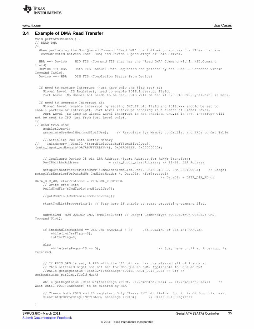
www.ti.com Use Cases
3.4 Example of DMA Read Transfervoid performDmaRead() {// READ DMA/*When performing the Non-Queued Command "Read DMA" the following captures the FISes that arecommunicated between Host (HBA) and Device (SpeedBridge or SATA Drive).
HBA ==> Device H2D FIS (Command FIS that has the "Read DMA" Command within H2D.Commandfield).Device ==> HBA Data FIS (Actual Data Requested and pointed by the DMA/PRD Contents within
Command Table).Device ==> HBA D2H FIS (Completion Status from Device)
If need to capture Interrupt (just have only the Flag set) at:Global Level (IS Register), need to enable P0IE.Interrupt field.Port Level (No Enable bit needs to be set. P0IS will be set if D2H FIS DW0.Byte1.bit6 is set).
If need to generate Interrupt at:Global Level (enable interrupt by setting GHC.IE bit field and P0IE.xxx should be set to
enable particular interrupt). Port Level interrupt handling is a subset of Global Level.Port Level (So long as Global Level interrupt is not enabled, GHC.IE is set, Interrupt will
not be sent to CPU just from Port Level only).*/// Read from Disk
cmdSlot2Use=1;associateSysMem2Hba(cmdSlot2Use); // Associate Sys Memory to CmdList and PRDs to Cmd Table
//Initialize PRD Data Buffer Memory// initMemory((Uint32 *)&prdTableDataBuff[cmdSlot2Use],(sata_input_prdLength*DATABUFFERLEN/4), 0xDEADBEEF, 0x00000000);
// Configure Device 28 bit LBA Address (Start Address for Rd/Wr Transfer);Dev28bitLbaAddress = sata_input_startAddress; // 28-Bit LBA Address
setupCfisEntriesForDataRdWr(&CmdLists[cmdSlot2Use], DATA_DIR_RD, DMA_PROTOCOL); // Usage:setupCfisEntriesForDataRdWr(CmdListHeader *, DataDir, xferProtocol)
// DataDir = DATA_DIR_RD orDATA_DIR_WR, xferProtocol = PIO/DMA_PROTOCOL
// Write cfis DatabuildCmdFis(&CmdTable[cmdSlot2Use]);
//getCmdFis(&CmdTable[cmdSlot2Use]);
startCmdListProcessing(); // Stay here if unable to start processing command list.
submitCmd (NON_QUEUED_CMD, cmdSlot2Use); // Usage: CommandType (QUEUED(NON_QUEUED)_CMD,Command Slot);
if(intHandlingMethod == USE_INT_HANDLER) { // USE_POLLING or USE_INT_HANDLERwhile(intIsrFlag==0);intIsrFlag=0;
}else
while(sataRegs->IS == 0); // Stay here until an interrupt isreceived.
// If P0IS.DPS is set, A PRD with the 'I' bit set has transferred all of its data.// This bitfield might not bit set for Non-Queued DMA. Applicable for Queued DMA//while(getRegStatus((Uint32*)&sataRegs->P0IS, AHCI_P0IS_DPS) == 0); //
getRegStatus(ptr2int,field Mask)
while(getRegStatus((Uint32*)&sataRegs->P0CI, (1<<cmdSlot2Use)) == (1<<cmdSlot2Use)); //Wait Until P0CI[ChHeader] to be cleared by HBA
// Clears both P0IS and IS register. Only Clears RWC bit fields. So, it is OK for this task.clearIntOrErrorDiag(INTFIELDS, sataRegs->P0IS); // Clear P0IS Register
}
35SPRUGJ8C–March 2011 Serial ATA (SATA) ControllerSubmit Documentation Feedback
© 2011, Texas Instruments Incorporated

Registers www.ti.com
4 Registers
Due to the support of a standard controller, that is compliant with the AHCI 1.1 specifications, thememory-map of the controller and the register descriptions matches the memory-map documented withinthe standard. For features that are not part of the standard, for example, DMA burst control or built-in selftest, the reserved locations are used to document the necessary registers required by the non-standardfeatures.
The subsystem core contains register space for global host programming and space for port programming(this device supports a single Host Port, but the AHCI specification calls for the support of multiple Hostports and the register space partitioning comes from this perspective). All registers that start below offsetaddress 100h are global and meant to apply to the entire HBA. The port control registers are the same forall ports and there are as many register banks as there are ports for hosts with multiple ports. This devicesupports only one HBA port and has a single register bank for Port 0. Table 3 shows the single bank ofregisters that are available for use.
Table 3. SATASS Memory Summary
Module Name Base Address Size
SATA Core (Global) 01E1 8000h 256 Bytes
SATA Port 0 01E1 8100h 128 Bytes
Table 4 lists the registers in the subsystem. Note that a special class of registers whose reset state islisted as W/RO (write/read only) requires a one time initialization after power-up. These registers arewritten once after a hard reset by firmware, and then remain as read-only thereafter; these registers arenot affected by software reset.
36 Serial ATA (SATA) Controller SPRUGJ8C–March 2011Submit Documentation Feedback
© 2011, Texas Instruments Incorporated

www.ti.com Registers
Table 4. SATA Controller Registers
AddressOffset Acronym Register Description Section
0 CAP HBA Capabilities Register Section 4.1
4h GHC Global HBA Control Register Section 4.2
8h IS Interrupt Status Register Section 4.3
Ch PI Ports Implemented Register Section 4.4
10h VS AHCI Version Register Section 4.5
14h CCC_CTL Command Completion Coalescing Control Register Section 4.6
18h CCC_PORTS Command Completion Coalescing Ports Register Section 4.7
A0h BISTAFR BIST Active FIS Register Section 4.8
A4h BISTCR BIST Control Register Section 4.9
A8h BISTFCTR BIST FIS Count Register Section 4.10
ACh BISTSR BIST Status Register Section 4.11
B0h BISTDECR BIST DWORD Error Count Register Section 4.12
E0h TIMER1MS BIST DWORD Error Count Register Section 4.13
E8h GPARAM1R Global Parameter 1 Register Section 4.14
ECh GPARAM2R Global Parameter 2 Register Section 4.15
F0h PPARAMR Port Parameter Register Section 4.16
F4h TESTR Test Register Section 4.17
F8h VERSIONR Version Register Section 4.18
FCh IDR ID Register Section 4.19
100h P0CLB Port Command List Base Address Register Section 4.20
108h P0FB Port FIS Base Address Register Section 4.21
110h P0IS Port Interrupt Status Register Section 4.22
114h P0IE Port Interrupt Enable Register Section 4.23
118h P0CMD Port Command Register Section 4.24
120h P0TFD Port Task File Data Register Section 4.25
124h P0SIG Port Signature Register Section 4.26
128h P0SSTS Port Serial ATA Status Register Section 4.27
12Ch P0SCTL Port Serial ATA Control Register Section 4.28
130h P0SERR Port Serial ATA Error Register Section 4.29
134h P0SACT Port Serial ATA Active Register Section 4.30
138h P0CI Port Command Issue Register Section 4.31
13Ch P0SNTF Port Serial ATA Notification Register Section 4.32
170h P0DMACR Port DMA Control Register Section 4.33
178h P0PHYCR Port PHY Control Register Section 4.34
17Ch P0PHYSR Port PHY Status Register Section 4.35
37SPRUGJ8C–March 2011 Serial ATA (SATA) ControllerSubmit Documentation Feedback
© 2011, Texas Instruments Incorporated

Registers www.ti.com
4.1 HBA Capabilities Register (CAP)
The HBA capabilities register (CAP) indicates basic capabilities of the DWC SATA AHCI to the driversoftware. The CAP is shown in Figure 3 and described in Table 5.
Figure 3. HBA Capabilities Register (CAP)31 30 29 28 27 26 25 24 23 20 19 18 17 16
S64A SNCQ SSNTF SMPS SSS SALP SAL SCLO ISS SNZO SAM SPM Rsvd
R-0 R-1 R-1 W/RO-0 W/RO-0 R-1 R-1 R-1 R-2h R-0 R-1 R-1 R-0
15 14 13 12 8 7 6 5 4 0
PMD SSC PSC NCS CCCS EMS SXS NP
R-1 R-1 R-1 R-1Fh R-1 R-0 R-0 R-0
LEGEND: R/W = Read/Write; R = Read only; W/RO: written once after hard reset by firmware, then remain as read-only;-n = value after reset
Table 5. HBA Capabilities Register (CAP) Field Descriptions
Bit Field Value Description
31 S64A 0 Indicates Support for 64-Bit Addressing. The SATASS only supports 32-bit addressing so this bit isalways 0.
30 SNCQ 1 Supports Native Command Queuing. SATASS supports SATA native command queuing by handlingDMA Setup FIS natively.
29 SSNTF 1 Supports SNotification Register. SATASS supports P0SNTF (SNotification) register and its associatedfunctionality.
28 SMPS 0 Supports Mechanical Presence Switch. This bit is set by firmware when the platform supports amechanical presence switch for hot plug operation.
27 SSS 0 Supports Staggered Spin-Up. Only writable once after power up.
26 SALP 1 Supports Aggressive Link Power Management. SATASS supports auto-generating (Port-initiated) LinkLayer requests to the PARTIAL or SLUMBER power management states when there are no commandsto process.
25 SAL 1 Supports Activity LED.
24 SCLO 1 Supports Command List Override. Supports the P0CMD.CLO bit functionality for Port Multiplier devicesenumeration.
23-20 ISS 2h Interface Speed Support. SATASS Supports 1.5 and 3 Gbps.
19 SNZO 0 Supports Non-Zero DMA Offsets. Not supported.
18 SAM 1 Supports AHCI Mode Only. SATASS supports AHCI mode only and does not support legacy, task-filebased register interface.
17 SPM 1 Supports Port Multiplier. SATASS supports command-based switching Port Multiplier on any of itsPorts.
16 Reserved 0 Reserved.
15 PMD 1 PIO Multiple DRQ Block. SATASS supports multiple DRQ block data transfers for the PIO commandprotocol.
14 SSC 1 Slumber State Capable. SATASS supports transitions to the interface SLUMBER power managementstate.
13 PSC 1 Partial State Capable. SATASS supports transitions to the interface PARTIAL power managementstate.
12-8 NCS 1Fh Number of Command Slots. SATASS supports 32 command slots per Port.
7 CCCS 1 Command Completion Coalescing Supported. SATASS supports command completion coalescing.
6 EMS 0 Enclosure Management Supported. Enclosure Management is not supported.
5 SXS 0 Supports External SATA.
4-0 NP Number of Ports. Indicates the number of Ports supported by the SATSS.
0 1 Port
38 Serial ATA (SATA) Controller SPRUGJ8C–March 2011Submit Documentation Feedback
© 2011, Texas Instruments Incorporated

www.ti.com Registers
4.2 Global HBA Control Register (GHC)
The global HBA control register (GHC) provides various global functions for the SATASS. The GHC isshown in Figure 4 and described in Table 6.
Figure 4. Global HBA Control Register (GHC)31 30 16
AE Reserved
R-1 R-0
15 2 1 0
Reserved IE HR
R-0 R/W-0 W-0
LEGEND: R/W = Read/Write; R = Read only; W = Write only; -n = value after reset
Table 6. Global HBA Control Register (GHC) Field Descriptions
Bit Field Value Description
31 AE 1 AHCI Enable. This bit is always set since SATASS supports only AHCI mode as indicated by the SAMbit in the HBA capabilities register (CAP) = 1.
30-2 Reserved 0 Reserved.
1 IE Interrupt Enable. This global bit enables interrupts from the SATASS. This field is reset on Global reset(GHC.HR = 1).
0 All interrupt sources from all the Ports are disabled (masked).
1 Interrupts are enabled and any SATASS interrupt event causes interrupt output assertion.
0 HR 0 HBA Reset. When set by the software, this bit causes an internal Global reset of the SATASS. All statemachines that relate to data transfers and queuing return to an idle state, and all the Ports arereinitialized by sending COMRESET if staggered spin-up is not supported. If staggered spin-up issupported, then it is the responsibility of the software to spin-up each Port after this reset hascompleted. The SATASS clears this bit when the reset action is done. A software write of 0 has noeffect.
39SPRUGJ8C–March 2011 Serial ATA (SATA) ControllerSubmit Documentation Feedback
© 2011, Texas Instruments Incorporated

Registers www.ti.com
4.3 Interrupt Status Register (IS)
The interrupt status register (IS) indicates which port inside of the subsystem has a pending interrupt. TheIS is shown in Figure 5 and described in Table 7.
Figure 5. Interrupt Status Register (IS)31 16
Reserved
R-0
15 2 1 0
Reserved IPS[n]
R-0 R/W1C-0
LEGEND: R/W = Read/Write; R = Read only; W1C = Write 1 to clear; -n = value after reset
Table 7. Interrupt Status Register (IS) Field Descriptions
Bit Field Value Description
31-2 Reserved 0 Reserved.
1-0 IPS[n] 0-1 Interrupt Pending Status. If a bit n is set to 1 If set, the corresponding Port has an interrupt pending.Software can use this information to determine which Ports require service after an interrupt. The bits ofthis field are set by the Ports that have interrupt events pending in the port interrupt status register(P0IS) bits and enabled by the port interrupt enable register (P0IE) bits. Set bits are cleared by thesoftware writing 1 to all bits to clear.
40 Serial ATA (SATA) Controller SPRUGJ8C–March 2011Submit Documentation Feedback
© 2011, Texas Instruments Incorporated

www.ti.com Registers
4.4 Ports Implemented Register (PI)
The ports implemented register (PI) indicates which ports are exposed by the SATASS and are availablefor software to use. It is loaded by the BIOS. For example, if the SATASS supports 8 Ports as indicated inthe CAP.NP, only Ports 1, 3, 5, and 7 could be available, while Ports 0, 2, 4, and 6 being unavailable.Note that this sub-system only has a single port so software should write a 0x1 to this bit at power-up. ThePI is shown in Figure 6 and described in Table 8.
Figure 6. Ports Implemented Register (PI)31 16
Reserved
R-0
15 2 1 0
Reserved PI[n]
R-0 W/RO-0
LEGEND: R/W = Read/Write; R = Read only; W/RO: written once after hard reset by firmware, then remain as read-only;-n = value after reset
Table 8. Ports Implemented Register (PI) Field Descriptions
Bit Field Value Description
31-2 Reserved 0 Reserved.
1-0 PI[n] 0-1 Ports Implemented. This register is bit significant. If a bit n is set to 1, the corresponding Port isavailable for software to use. If a bit n is cleared to 0, the Port is not available for software to use. Themaximum number of bits that can be set to 1 is CAP.NP + 1. At least one bit must be set to 1. Thecontents of this register are relevant to the command completion coalescing ports register(CCC_PORTS).
4.5 AHCI Version Register (VS)
The AHCI version register (VS) indicates the version of the Synopsis AHCI core embedded in theSATASS. The VS is shown in Figure 7 and described in Table 9.
Figure 7. AHCI Version Register (VS)31 16
MJR
R-1
15 0
MNR
R-100h
LEGEND: R = Read only; -n = value after reset
Table 9. AHCI Version Register (VS) Field Descriptions
Bit Field Value Description
31-16 MJR 1 Major Revision Number.
15-0 MNR 100h Minor Revision Number.
41SPRUGJ8C–March 2011 Serial ATA (SATA) ControllerSubmit Documentation Feedback
© 2011, Texas Instruments Incorporated

Registers www.ti.com
4.6 Command Completion Coalescing Control Register (CCC_CTL)
The command completion coalescing control register (CCC_CTL) is used to configure the commandcompletion coalescing (CCC) feature for the SATASS core. It is reset on Global reset. The CCC_CTL isshown in Figure 8 and described in Table 10.
Figure 8. Command Completion Coalescing Control Register (CCC_CTL)31 16
TV
R/W-1
15 8 7 3 2 1 0
CC INT Reserved EN
R/W-1 R-1 R-0 R/W-0
LEGEND: R/W = Read/Write; R = Read only; -n = value after reset
Table 10. Command Completion Coalescing Control Register (CCC_CTL) Field Descriptions
Bit Field Value Description
31-16 TV 0-FFFFh Time-out value. This bit field specifies the CCC time-out value in 1 ms intervals. Software loadsthis value prior to enabling CCC. This bit field is:
• Read/Write (R/W) when EN = 0• Read only (R) when EN = 1
A time-out value of 0 is reserved and should not be used.
15-8 CC 0-FFh Command Completions. This bit field specifies the number of command completions that arenecessary to cause a CCC interrupt. Software loads this value prior to enabling CCC. This bit fieldis:
• Read/Write (R/W) when EN = 0• Read only (R) when EN = 1
A value of 0 disables CCC interrupts being generated based on the number of commandscompleted, that is, CCC interrupts are only generated based on the timer in this case.
7-3 INT 0-1Fh Interrupt. This bit field specifies the interrupt used by the CCC feature, using the number of portsconfigured for the core. For a single Port instantiation, INT should be programmed to 1.
When a CCC interrupt occurs, the IS.IPS[INT] bit is set to 1.
2-1 Reserved 0 Reserved.
0 EN CCC feature enable. When EN = 1, software can not change the bit fields: TV and CC.
0 CCC feature is disabled and no CCC interrupts are generated.
1 CCC feature is enabled and CCC interrupts may be generated based on the time-out or commandcompletion conditions.
42 Serial ATA (SATA) Controller SPRUGJ8C–March 2011Submit Documentation Feedback
© 2011, Texas Instruments Incorporated

www.ti.com Registers
4.7 Command Completion Coalescing Ports Register (CCC_PORTS)
The command completion coalescing ports register (CCC_PORTS) specifies the Ports that are coalescedas part of the command completion coalescing (CCC) feature when CCC_CTL.EN = 1. It is reset onGlobal reset. The CCC_PORTS is shown in Figure 9 and described in Table 11.
Figure 9. Command Completion Coalescing Ports Register (CCC_PORTS)31 0
PRT[n]
R/W-0
LEGEND: R/W = Read/Write; -n = value after reset
Table 11. Command Completion Coalescing Ports Register (CCC_PORTS) Field Description
Bit Field Value Description
31-0 PRT[n] Ports. This field is bit significant. Each bit n corresponds to a particular Port, where bit 0 corresponds toPort0. Bits set to 1 must also have the corresponding bit set to 1 in the ports implemented register (PI).
0 The corresponding Port is not part of the CCC feature.
1 The corresponding Port is part of the CCC feature.
43SPRUGJ8C–March 2011 Serial ATA (SATA) ControllerSubmit Documentation Feedback
© 2011, Texas Instruments Incorporated

Registers www.ti.com
4.8 BIST Active FIS Register (BISTAFR)
The BIST active FIS register (BISTAFR) is shown in Figure 10 and described in Table 12.
Figure 10. BIST Active FIS Register (BISTAFR)31 16
Reserved
R-0
15 8 7 0
NCP PD
R-0 R-0
LEGEND: R = Read only; -n = value after reset
Table 12. BIST Active FIS Register (BISTAFR) Field Descriptions
Bit Field Value Description
31-16 Reserved 0 Reserved.
15-8 NCP 0-FFh Non-Compliant Pattern. Least significant byte of the received BIST Activate FIS second DWORD(bits [7:0]). This value defines the required pattern for the far-end transmit only modes (PD=80h orA0h). If the following reserved values are decoded, the simultaneous switching pattern istransmitted by default.
0-49h Reserved
4Ah High frequency test pattern (HFTP)
4Bh-77h Reserved
78h Mid frequency test pattern (MFTP)
79h-7Dh Reserved
7Eh Low frequency test pattern (LFTP)
7Fh Simultaneous switching outputs pattern (SSOP)
80h-8Ah Reserved
8Bh Lone Bit pattern (LBP)
8Ch-AAh Reserved
ABh Low frequency spectral component pattern (LFSCP)
ACh-B4h Reserved
B5h High transition density pattern (HTDP)
B6h-F0h Reserved
F1h Low transition density pattern (LTDP)
F2h-FFh Reserved
7-0 PD 0-FFh Pattern Definition. Indicates the pattern definition field of the received BIST Activate FIS (bits[23:16]) of the first DWORD. It is used to put the SATASS in one of the following BIST modes. Allreserved values should not be used by the device; otherwise, the FIS is negatively acknowledgedwith R_ERRp. For far-end transmit only modes, the NCP bit field contains the required datapattern.
0-7h Reserved
8h Far-end analog (if PHY supports this mode)
9h-Fh Reserved
10h Far-end retimed
11h-7Fh Reserved
80h Far-end transmit only
81h-9Fh Reserved
A0h Far-end transmit only with scrambler bypassed
A1h-FFh Reserved
44 Serial ATA (SATA) Controller SPRUGJ8C–March 2011Submit Documentation Feedback
© 2011, Texas Instruments Incorporated

www.ti.com Registers
4.9 BIST Control Register (BISTCR)
The BIST control register (BISTCR) is shown in Figure 11 and described in Table 13.
Figure 11. BIST Control Register (BISTCR)31 24
Reserved
R-0
23 19 18 17 16
Reserved TXO CNTCLR NEALB
R-0 W-0 W-0 R/W-0
15 11 10 8
Reserved LLC
R-0 R/W-7h
7 6 5 4 3 0
Reserved ERREN FLIP PV PATTERN
R-0 R/W-0 R/W-0 R/W-0 R/W-0
LEGEND: R/W = Read/Write; R = Read only; W = Write only; -n = value after reset
Table 13. BIST Control Register (BISTCR) Field Descriptions
Bit Field Value Description
31-19 Reserved 0 Reserved.
18 TXO 0 Transmit Only. This bit is used to initiate transmission of one of the non-compliant patterns defined bythe BISTCR.PATTERN value when the device is disconnected.
17 CNTCLR 0 Counter Clear. This bit clears BIST error count registers. Writing a 1 clears BISTFCTR, BISTSR, andBISTDECR registers.
16 NEALB Near-end Analog Loopback. Places the Port PHY into near-end analog loopback mode.
0 Near-end analog loopback is not requested.
1 Initiates a near-end analog loopback request. BISTCR.CP field contains the appropriate pattern. Thismode should be initiated either in the PARTIAL or SLUMBER power mode, or with the devicedisconnected from the Port PHY (Link NOCOMM state). BIST Activate FIS is not sent to the device inthis mode.
15-11 Reserved 0 Reserved.
10-8 LLC 0-7h Link Layer Control. This bit field controls the Port Link Layer functions: scrambler, descrambler, andrepeat primitive drop (RPD). In normal mode, the functions scrambler, descrambler, or RPD arechanged only during Port reset (P0SCTL.DET = 1). Note the different meanings for normal and BISTmodes of operation:
Bit 10 (RPD):
0 Repeat primitive drop function is disabled in normal mode, enabled in BIST mode.
1 Repeat primitive drop function is enabled in normal mode, disabled in BIST mode.
Bit 9 (DESCRAM):
0 Descrambler is disabled in normal mode, enabled in BIST mode.
1 Descrambler is enabled in normal mode, disabled in BIST mode.
Bit 8 (SCRAM):
0 Scrambler is disabled in normal mode, enabled in BIST mode.
1 Scrambler is enabled in normal mode, disabled in BIST mode.
The SCRAM bit is cleared (enabled) by the Port when the Port enters a responder far-end transmitBIST mode with scrambling enabled (BISTAFR.PD = 80h).
7 Reserved 0 Reserved.
6 ERREN Error Enable. Used to allow or filter (disable) PHY internal errors outside the FIS boundary to setcorresponding port serial ATA error register (P0SERR) bits.
0 Filter errors outside the FIS, allow errors inside the FIS.
1 Allow errors outside or inside the FIS.
45SPRUGJ8C–March 2011 Serial ATA (SATA) ControllerSubmit Documentation Feedback
© 2011, Texas Instruments Incorporated

Registers www.ti.com
Table 13. BIST Control Register (BISTCR) Field Descriptions (continued)
Bit Field Value Description
5 FLIP 0-1 Flip Disparity. Enables changing disparity of the current test pattern to the opposite every time its stateis changed by software.
4 PV Pattern Version. Selects either short or long version of the SSOP, HTDP, LTDP, LFSCP, and COMPpatterns.
0 Short pattern version
1 Long pattern version
3-0 PATTERN 0-Fh Defines one of the following SATA compliant patterns for far-end retimed/ far-end analog/near-endanalog initiator modes, or non-compliant patterns for transmit-only responder mode when initiated bysoftware writing to the BISTCR.TXO bit.
0 Simultaneous switching outputs pattern (SSOP)
1h High-transition density pattern
2h Low-transition density pattern
3h Low-frequency spectral component pattern (LFSCP)
4h Composite pattern (COMP)
5h Lone bit pattern (LBP)
6h Mid-frequency test pattern (MFTP)
7h High-frequency test pattern (HFTP)
8h Low-frequency test pattern (LFTP)
9h-Fh Reserved.
46 Serial ATA (SATA) Controller SPRUGJ8C–March 2011Submit Documentation Feedback
© 2011, Texas Instruments Incorporated

www.ti.com Registers
4.10 BIST FIS Count Register (BISTFCTR)
The BIST FIS count register (BISTFCTR) contains the received BIST FIS count in the loopback initiatorfar-end retimed, far-end analog and near-end analog modes. It is updated each time a new BIST FIS isreceived. It is reset by Global reset, Port reset (COMRESET) or by setting the BISTCR.CNTCLR bit. Thisregister does not roll over and freezes when the FFFF FFFFh value is reached. It takes approximately 65hours of continuous BIST operation to reach this value. The BISTFCTR is shown in Figure 12 anddescribed in Table 14.
Figure 12. BIST FIS Count Register (BISTFCTR)31 0
BISTFCTR
R/W-0
LEGEND: R/W = Read/Write; -n = value after reset
Table 14. BIST FIS Count Register (BISTFCTR) Field Description
Bit Field Value Description
31-0 BISTFCTR 0-FFFF FFFFh Received BIST FIS Count.
4.11 BIST Status Register (BISTSR)
The BIST status register (BISTSR) contains errors detected in the received BIST FIS in the loopbackinitiator far-end retimed, far-end analog and near-end analog modes. It is updated each time a new BISTFIS is received. It is reset by Global reset, Port reset (COMRESET) or by setting the BISTCR.CNTCLR bit.The BISTSR is shown in Figure 13 and described in Table 15.
Figure 13. BIST Status Register (BISTSR)31 24 23 16
Reserved BRSTERR
R-0 R-0
15 0
FRAMERR
W-0
LEGEND: R = Read only; W = Write only; -n = value after reset
Table 15. BIST Status Register (BISTSR) Field Description
Bit Field Value Description
31-24 Reserved 0 Reserved.
23-16 BRSTERR 0-FFh Burst Error. This bit field contains the burst error count. It is accumulated each time a burst errorcondition is detected: DWORD error is detected in the received frame and 1.5 seconds (27,000frames) passed since the previous burst error was detected. The BRSTERR value does not rollover and freezes at FFh. This bit field is updated if BIST_MODE = DWORD.
15-0 FRAMERR 0-FFFFh Frame Error. This bit field contains the frame error count. It is accumulated (new value is added tothe old value) each time a new BIST frame with a CRC error is received. The FRAMERR valuedoes not roll over and freezes at FFFFh.
47SPRUGJ8C–March 2011 Serial ATA (SATA) ControllerSubmit Documentation Feedback
© 2011, Texas Instruments Incorporated

Registers www.ti.com
4.12 BIST DWORD Error Count Register (BISTDECR)
The BIST DWORD error count register (BISTDECR) contains the number of DWORD errors detected inthe received BIST frame in the loopback initiator far-end retimed, far-end analog and near-end analogmodes. It is updated each time a new BIST frame is received. It is reset by Global reset, Port reset(COMRESET) or by setting the BISTCR.CNTCLR bit. This register is updated only when the parameterBIST_MODE=DWORD. The BISTDECR is shown in Figure 14 and described in Table 16.
Figure 14. BIST DWORD Error Count Register (BISTDECR)31 0
DWERR
R-0
LEGEND: R = Read only; -n = value after reset
Table 16. BIST DWORD Error Count Register (BISTDECR) Field Description
Bit Field Value Description
31-0 DWERR 0-FFFF FFFFh DWORD Error Count. This bit field contains the DWORD error count. It is accumulated (newvalue is added to the old value) each time a new BIST frame is received. The DWERR valuedoes not roll over and freezes if it exceeds FFFF F000h.
4.13 BIST DWORD Error Count Register (TIMER1MS)
The BIST DWORD error count register (TIMER1MS) is used to generate 1ms tick for the commandcompletion coalescing (CCC) logic based on the VBUS clock frequency sourced to the SATA Controller.Software must initialize this register with the required value after power up before using the CCC feature.This register is reset to 100,000d (corresponding to a VBUS Clock frequency of 100 MHz hclk) on powerup and is not affected by Global reset. The TIMER1MS is shown in Figure 15 and described in Table 17.
Figure 15. BIST DWORD Error Count Register (TIMER1MS)31 20 19 0
Reserved TIMV
R-0 R/W-186A0h
LEGEND: R/W = Read/Write; R = Read only; -n = value after reset
Table 17. BIST DWORD Error Count Register (TIMER1MS) Field Description
Bit Field Value Description
31-20 Reserved 0 Reserved.
19-0 TIMV 0-F FFFFh 1ms Timer Value. This bit field contains the cycle count of the SATA VBUS Clock Cycle generating1ms tick. This bit field is:
• Read/Write (R/W) when CCC_CTL.EN = 0• Read only (R) when CCC_CTL.EN = 1
48 Serial ATA (SATA) Controller SPRUGJ8C–March 2011Submit Documentation Feedback
© 2011, Texas Instruments Incorporated
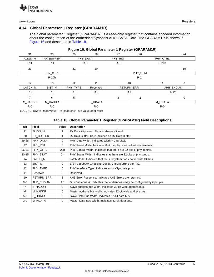
www.ti.com Registers
4.14 Global Parameter 1 Register (GPARAM1R)
The global parameter 1 register (GPARAM1R) is a read-only register that contains encoded informationabout the configuration of the embedded Synopsis AHCI SATA Core. The GPARAM1R is shown inFigure 16 and described in Table 18.
Figure 16. Global Parameter 1 Register (GPARAM1R)31 30 29 28 27 26 24
ALIGN_M RX_BUFFER PHY_DATA PHY_RST PHY_CTRL
R-1 R-1 R-0 R-0 R-20h
23 21 20 15
PHY_CTRL PHY_STAT
R-20h R-2h
14 13 12 11 10 9 8
LATCH_M BIST_M PHY_TYPE Reserved RETURN_ERR AHB_ENDIAN
R-0 R-0 R-0 R-0 R-1 R-2h
7 6 5 3 2 0
S_HADDR M_HADDR S_HDATA M_HDATA
R-0 R-0 R-0 R-0
LEGEND: R/W = Read/Write; R = Read only; -n = value after reset
Table 18. Global Parameter 1 Register (GPARAM1R) Field Descriptions
Bit Field Value Description
31 ALIGN_M 1 Rx Data Alignment. Data is always aligned.
30 RX_BUFFER 1 Rx Data Buffer. Core includes an Rx Data Buffer.
29-28 PHY_DATA 0 PHY Data Width. Indicates width = 0 (8-bits).
27 PHY_RST 0 PHY Reset Mode. Indicates that the phy reset output is active-low.
26-21 PHY_CTRL 20h PHY Control Width. Indicates that there are 32-bits of phy control.
20-15 PHY_STAT 2h PHY Status Width. Indicates that there are 32-bits of phy status.
14 LATCH_M 0 Latch Mode. Indicates that the subsystem does not include latches.
13 BIST_M 0 BIST Loopback Checking Depth. Checks errors per FIS.
12 PHY_TYPE 0 PHY Interface Type. Indicates a non-Synopsis phy.
11 Reserved 0 Reserved.
10 RETURN_ERR 1 AHB Error Response. Indicates AHB Errors are returned.
9-8 AHB_ENDIAN 2h Bus Endianness. Indicates that endianness may be configured by input pin.
7 S_HADDR 0 Slave address bus width. Indicates 32-bit wide address bus.
6 M_HADDR 0 Master address bus width. Indicates 32-bit wide address bus.
5-3 S_HDATA 0 Slave Data Bus Width. Indicates 32-bit data bus.
2-0 M_HDATA 0 Master Data Bus Width. Indicates 32-bit data bus.
49SPRUGJ8C–March 2011 Serial ATA (SATA) ControllerSubmit Documentation Feedback
© 2011, Texas Instruments Incorporated

Registers www.ti.com
4.15 Global Parameter 2 Register (GPARAM2R)
The global parameter 2 register (GPARAM2R) is a read-only register that contains encoded informationabout the configuration of the embedded Synopsis AHCI SATA Core. The GPARAM2R is shown inFigure 17 and described in Table 19.
Figure 17. Global Parameter 2 Register (GPARAM2R)31 16
Reserved
R-0
15 14 13 12 11 10 9
Reserved DEV_CP DEV_MP ENCODE_M RXOOB_CLK_M RXOOB_M TX_OOB_M
R-0 R-1 R-1 R-1 R-0 R-0 R-1
8 0
RXOOB_CLK
R-96h
LEGEND: R = Read only; -n = value after reset
Table 19. Global Parameter 2 Register (GPARAM2R) Field Descriptions
Bit Field Value Description
31-15 Reserved 0 Reserved.
14 DEV_CP 1 Cold Presence Detect. CPD is supported in SATASS.
13 DEV_MP 1 Mechanical Presence Switch. MP is supported in SATASS.
12 ENCODE_M 1 8b/10b Encoding/Decoding. Indicates 8-bit/10-bit encoding and decoding are done in the Synopsiscore.
11 RXOOB_CLK_M 0 Rx OOB Clock Mode. Indicates that the Rx OOB Functions are on the Rx Clock.
10 RX_OOB_M 0 Rx OOB Mode. Indicates that Rx Out-of-Band signals are detected in the phy.
9 TX_OOB_M 1 Tx OOB Mode. Indicates that Tx Out-of-Band signaling is done by the Synopsis Core.
8-0 RXOOB_CLK 96h Rx OOB Clock Frequency. Reflects the hexadecimal value of the RXOOB_CLK_FREQ parameter.
50 Serial ATA (SATA) Controller SPRUGJ8C–March 2011Submit Documentation Feedback
© 2011, Texas Instruments Incorporated

www.ti.com Registers
4.16 Port Parameter Register (PPARAMR)
The port parameter register (PPARAMR) is a read-only register that contains encoded information aboutthe selected Port configuration parameters settings. The Port is selected by the TESTR.PSEL field. Note,there is only one port on this sub-system. The PPARAMR is shown in Figure 18 and described inTable 20.
Figure 18. Port Parameter Register (PPARAMR)31 16
Reserved
R-0
15 10 9 8
Reserved TX_MEM_M TX_MEM_S
R-0 R-0 R-0
7 6 5 3 2 0
RX_MEM_M RX_MEM_S X_FIFO_DEPTH RX_FIFO_DEPTH
R-0 R-0 R-0 R-1
LEGEND: R = Read only; -n = value after reset
Table 20. Port Parameter Register (PPARAMR) Field Descriptions
Bit Field Value Description
31-10 Reserved 0 Reserved.
9 TX_MEM_M 0 Tx FIFO Memory Read Port Type. Indicates that the Tx FIFO memory is asynchronous read.
8 TX_MEM_S 0 Tx FIFO Memory Type. Indicates that the Tx FIFO memory is outside of the core (but still insidethe subsystem wrapper).
7 RX_MEM_M 0 Rx FIFO Memory Read Port Type. Indicates that the Rx FIFO memory is asynchronous read.
6 RX_MEM_S 0 Rx FIFO Memory Type. Indicates that the Rx FIFO memory is outside of the core (but stillinside the subsystem wrapper).
5-3 TX_FIFO_DEPTH 0 Tx FIFO Depth. Indicates that the depth of the Tx FIFO is 32 DWORDS.
2-0 RX_FIFO_DEPTH 1 Rx FIFO Depth. Indicates that the depth of the Rx FIFO is 64 DWORDS.
51SPRUGJ8C–March 2011 Serial ATA (SATA) ControllerSubmit Documentation Feedback
© 2011, Texas Instruments Incorporated

Registers www.ti.com
4.17 Test Register (TESTR)
The test register (TESTR) is used to put the SATASS slave interface into a test mode and to select a Portfor BIST operation. The TESTR is shown in Figure 19 and described in Table 21.
Figure 19. Test Register (TESTR)31 19 18 16
Reserved PSEL
R-0 R/W-0
15 0
Reserved TEST_IF
R-0 R/W-0
LEGEND: R/W = Read/Write; R = Read only; -n = value after reset
Table 21. Test Register (TESTR) Field Descriptions
Bit Field Value Description
31-19 Reserved 0 Reserved.
18-16 PSEL 0 Port Select. Selects the port for BIST operation. Note that there is only one port in this subsystem, so 0is the only valid value.
15-1 Reserved 0 Reserved.
0 TEST_IF Test Interface. Places the DWC SATA AHCI slave interface into the test mode.
0 Normal mode: the read back value of some registers is a function of the DWC SATA AHCI state anddoes not match the value written.
1 Test mode: the read back value of the registers matches the value written. Normal operation isdisabled. The following registers are accessed in this mode:
• GHC register: IE bit• BISTAFR register: NCP and PD bits become read/write• BISTCR register: LLC, ERREN, FLIP, PV, PATTERN• BISTFCTR, BISTSR, BISTDECR registers become read/write• P0CLB/CLBU, P0FB/FBU registers• P0IS register: RW1C and UFS bits become read/write• P0IE register• P0CMD register: ASP, ALPE, DLAE, ATAPI, PMA bits• P0TFD, P0SIG registers become read/write• P0SCTL register• P0SERR register: R/W1C bits become read/write bits• P0SACT, P0CI, P0SNTF registers become read/write• P0DMACR register• P0PHYCR register• P0PHYSR register becomes read/write
Notes:
Interrupt is asserted if any of the IS register bits is set after setting the corresponding P0IS and P0IEregisters and GHC.IE = 1.
CAP.SMPS/SSS, PI, P0CMD.ESP/CPD/MPSP/ HPCP register bits are W/RO (written once afterpower-on reset, then remain as read-only) type and can not be used in test mode.
Global DWC SATA AHCI reset must be issued (GHC.HR = 1) after TEST_IF bit is cleared following thetest mode operation.
52 Serial ATA (SATA) Controller SPRUGJ8C–March 2011Submit Documentation Feedback
© 2011, Texas Instruments Incorporated

www.ti.com Registers
4.18 Version Register (VERSIONR)
The version register (VERSIONR) contains the 32-bit SATASS version. The VERSIONR is shown inFigure 20 and described in Table 22.
Figure 20. Version Register (VERSIONR)31 0
VERSION
R-3133 302Ah
LEGEND: R = Read only; -n = value after reset
Table 22. Version Register (VERSIONR) Field Description
Bit Field Value Description
31-0 VERSION 3133 302Ah Version of SATASS.
4.19 ID Register (IDR)
The ID register (IDR) contains the 32-bit SATASS ID. The IDR is shown in Figure 21 and described inTable 23.
Figure 21. ID Register (IDR)31 0
ID
R-4E40 4903h
LEGEND: R = Read only; -n = value after reset
Table 23. ID Register (IDR) Field Description
Bit Field Value Description
31-0 ID 4E40 4903h ID of SATASS.
53SPRUGJ8C–March 2011 Serial ATA (SATA) ControllerSubmit Documentation Feedback
© 2011, Texas Instruments Incorporated

Registers www.ti.com
4.20 Port Command List Base Address Register (P0CLB)
The port command list base address register (P0CLB) contains the 32-bit base address of the commandlist. The P0CLB is shown in Figure 22 and described in Table 24.
Figure 22. Port Command List Base Address Register (P0CLB)31 10 9 0
CLB Reserved
R/W-0 R-0
LEGEND: R/W = Read/Write; R = Read only; -n = value after reset
Table 24. Port Command List Base Address Register (P0CLB) Field Description
Bit Field Value Description
31-10 CLB 0-3F FFFFh Command List Base Address. Indicates the 32-bit base physical address for the command list forthis port. This base is used when fetching commands to execute. The structure pointed to by thisaddress range is 1Kbyte in length. This address must be 1Kbyte-aligned as indicated by bits [9:0]being read-only.
9-0 Reserved 0 Reserved.
4.21 Port FIS Base Address Register (P0FB)
The port FIS base address register (P0FB) contains the 32-bit base address of the destination forincoming received FISes. The P0FB is shown in Figure 23 and described in Table 25.
Figure 23. Port FIS Base Address Register (P0FB)31 8 7 0
FB Reserved
R/W-0 R-0
LEGEND: R/W = Read/Write; R = Read only; -n = value after reset
Table 25. Port FIS Base Address Register (P0FB) Field Description
Bit Field Value Description
31-8 FB 0-FF FFFFh FIS Base Address. Indicates the 32-bit base physical address for received FISes. The structurepointed to by this address range is 256 bytes in length. This address must be 256 byte-aligned asindicated by bits [7:0] being read-only.
7-0 Reserved 0 Reserved.
54 Serial ATA (SATA) Controller SPRUGJ8C–March 2011Submit Documentation Feedback
© 2011, Texas Instruments Incorporated

www.ti.com Registers
4.22 Port Interrupt Status Register (P0IS)
The port interrupt status register (P0IS) is used to generate SATASS interrupts when any of the bits areset. Bits in this register are set by some internal conditions, and cleared by software writing ones in thepositions it wants to clear. This register is reset on Global reset. The P0IS is shown in Figure 24 anddescribed in Table 26.
Figure 24. Port Interrupt Status Register (P0IS)31 30 29 28 27 26 25 24 23 22 21 16
CPDS TFES HBFS HBDS IFS INFS Rsvd OFS IPMS PRCS Reserved
R/W1C-0 R/W1C-0 R/W1C-0 R/W1C-0 R/W1C-0 R/W1C-0 R-0 R/W1C-0 R/W1C-0 R-0 R-0
15 8 7 6 5 4 3 2 1 0
Reserved DMPS PCS DPS UFS SDBS DSS PSS DHRS
R-0 R/W1C-0 R-0 R/W1C-0 R-0 R/W1C-0 R/W1C-0 R/W1C-0 R/W1C-0
LEGEND: R/W = Read/Write; R = Read only; W1C = Write 1 to clear; -n = value after reset
Table 26. Port Interrupt Status Register (P0IS) Field Descriptions
Bit Field Value Description
31 CPDS 0-1 Cold Port Detect Status. This bit is set when the external input changes its state due to the insertion orremoval of a device. This bit is only valid if the port supports cold presence detection as indicated by theP0CMD.CPD bit being set to 1.
30 TFES 0-1 Task File Error Status. This bit is set whenever the P0TFD register is updated by the device and theerror bit (P0TFD.STS[0]) is set.
29 HBFS 0-1 Host Bus Fatal Error Status. This bit is set when SATASS bus master detects an ERROR responsefrom the slave.
28 HBDS 0-1 Host Bus Data Error Status. This bit is always cleared to 0.
27 IFS 0-1 Interface Fatal Error Status. This bit is set if any of the following conditions is detected:
• SYNC escape is received from the device during H2D Register or Data FIS transmission.• One or more of the following errors are detected during Data FIS transfer: Protocol
(P0SERR.ERR_P), CRC (P0SERR.DIAG_C), Handshake (P0SERR.DIAG_H), PHY Not Ready(P0SERR.ERR_C).
• Unknown FIS is received with good CRC, but the length exceeds 64 bytes.• PRD table byte count is zero.
Port DMA transitions to a fatal state until software clears P0CMD.ST bit or resets the interface by wayof Port or Global reset.
26 INFS 0-1 Interface Non-fatal Error Status. This bit is set if any of the following conditions is detected:
• One or more of the following errors are detected during non-data FIS transfer: Protocol(P0SERR.ERR_P), CRC (P0SERR.DIAG_C), Handshake (P0SERR.DIAG_H), PHY Not Ready(P0SERR.ERR_C).
• Command list underflow during read operation (DMA read) when software builds command table thathas more total bytes than the transaction given to the device.
In both cases, Port operation continues normally. If error is detected during non-data FIS transmission,this FIS is retransmitted continuously until it succeeds or software times out and resets the interface.
25 Reserved 0 Reserved.
24 OFS 0-1 Overflow Status. This bit is set if command list overflow is detected during read or write operation whensoftware builds a command table that has fewer total bytes than the transaction given to the device.
Port DMA transitions to a fatal state until software clears P0CMD.ST bit or resets the interface by wayof Port or Global reset.
23 IPMS 0-1 Incorrect Port Multiplier Status. Indicates that the HBA received a FIS from a device whose PortMultiplier field did not match what was expected.
This bit may be set during enumeration of devices on a Port Multiplier due to the normal Port Multiplierenumeration process. The software should only use the IPMS bit after enumeration is complete on thePort Multiplier.
22 PRCS 0-1 PHYReady Change Status. When set to 1, indicates the internal PHY Ready signal changed state. Thisbit reflects the state of the P0SERR.DIAG_N bit. To clear this bit, the software must clear theP0SERR.DIAG_N bit to 0.
21-8 Reserved 0 Reserved.
55SPRUGJ8C–March 2011 Serial ATA (SATA) ControllerSubmit Documentation Feedback
© 2011, Texas Instruments Incorporated

Registers www.ti.com
Table 26. Port Interrupt Status Register (P0IS) Field Descriptions (continued)
Bit Field Value Description
7 DMPS 0-1 Device Mechanical Presence Status. This bit is set when the state of SATA_MP_SWITCH input pinchanges as a result of a mechanical switch attached to this port being opened or closed. This bit is onlyvalid if both CAP.SMPS and P0CMD.MPSP are set to 1.
6 PCS Port Connect Change Status. This bit reflects the state of the P0SERR.DIAG_X bit. This bit is onlycleared when P0SERR.DIAG_X is cleared.
0 No change in Current Connect Status
1 Change in Current Connect Status
5 DPS 0-1 Descriptor Processed. A PRD with the I bit set has transferred all of its data.
Note: This is an opportunistic interrupt and should not be used to definitely indicate the end of atransfer. Two PRD interrupts could happen close in time together such that the second interrupt ismissed when the first PRD interrupt is being cleared.
4 UFS 0-1 Unknown FIS Interrupt. When set to 1, indicates that an unknown FIS was received and has beencopied into system memory. This bit is cleared to 0 by software clearing the P0SERR.DIAG_F bit to 0.
Note: The UFS bit does not directly reflect the P0SERR.DIAG_F bit. P0SERR.DIAG_F bit is setimmediately when an unknown FIS is detected, whereas the UFS bit is set when that FIS is posted tomemory. Software should wait to act on an unknown FIS until the UFS bit is set to 1 or the two bits maybecome out of sync.
3 SDBS 0-1 Set Device Bits Interrupt. A Set Device Bits FIS has been received with the I bit set and has beencopied into system memory.
2 DSS 0-1 DMA Setup FIS Interrupt. A DMA Setup FIS has been received with the I bit set and has been copiedinto system memory.
1 PSS 0-1 PIO Setup FIS Interrupt. A PIO Setup FIS has been received with the I bit set, it has been copied intosystem memory, and the data related to that FIS has been transferred.
0 DHRS 0-1 Device to Host Register FIS Interrupt. A D2H Register FIS has been received with the I bit set, and hasbeen copied into system memory.
56 Serial ATA (SATA) Controller SPRUGJ8C–March 2011Submit Documentation Feedback
© 2011, Texas Instruments Incorporated

www.ti.com Registers
4.23 Port Interrupt Enable Register (P0IE)
The port interrupt enable register (P0IE) enables and disables the reporting of the corresponding interruptto system software. When a bit is set (1), and the corresponding interrupt condition is active, then theSATASS intrq output is asserted. Interrupt sources that are disabled (0) are still reflected in the statusregisters. This register is symmetrical with the P0IS register. This register is reset on Global reset. TheP0IE is shown in Figure 25 and described in Table 27.
Figure 25. Port Interrupt Enable Register (P0IE)31 30 29 28 27 26 25 24 23 22 21 16
CPDE TFEE HBFE HBDE IFE INFE Rsvd OFE IPME PRCE Reserved
R/W-0 R/W-0 R/W-0 R/W-0 R/W-0 R/W-0 R-0 R/W-0 R/W-0 R/W-0 R-0
15 8 7 6 5 4 3 2 1 0
Reserved DMPE PCE DPE UFE SDBE DSE PSE DHRE
R-0 R/W-0 R/W-0 R/W-0 R/W-0 R/W-0 R/W-0 R/W-0 R/W-0
LEGEND: R/W = Read/Write; R = Read only; -n = value after reset
Table 27. Port Interrupt Enable Register (P0IE) Field Descriptions
Bit Field Value Description
31 CPDE 0-1 Cold Port Detect Enable. When set to 1, GHC.IE = 1, and P0IS.CPDS = 1, the intrq output is asserted.
30 TFEE 0-1 Task File Error Enable. When set to 1, GHC.IE = 1, and P0IS.HBFS = 1, the intrq output is asserted.
29 HBFE 0-1 Host Bus Fatal Error Enable. When set to 1, GHC.IE = 1, and P0IS.HBFS = 1, the interq output isasserted.
28 HBDE 0-1 Host Bus Data Error Enable. When set to 1, GHC.IE = 1, and P0IS.HBDS = 1, the intrq output isasserted.
27 IFE 0-1 Interface Fatal Error Enable. When set to 1, GHC.IE = 1, and P0IS.IFS = 1, the intrq output is asserted.
26 INFE 0-1 Interface Non-fatal Error Enable. When set to 1, GHC.IE = 1, and P0IS.INFS = 1, the intrq output isasserted.
25 Reserved 0 Reserved.
24 OFE 0-1 Overflow Enable. When set to 1, GHC.IE = 1, and P0IS.OFS = 1, the intrq output is asserted.
23 IPME 0-1 Incorrect Port Multiplier Enable. When set to 1, GHC.IE = 1, and P0IS.IPMS = 1, the intrq output isasserted.
22 PRCE 0-1 PHYReady Change Enable. When set to 1, GHC.IE = 1, and P0IS.PRCS = 1, the intrq output isasserted.
21-8 Reserved 0 Reserved.
7 DMPE 0-1 Device Mechanical Presence Enable. When set to 1, GHC.IE = 1, and P0IS.DMPS = 1, the intrq outputis asserted.
6 PCE 0-1 Port Change Interrupt Enable. When set to 1, GHC.IE = 1, and P0IS.PCS = 1, the intrq output isasserted.
5 DPE 0-1 Descriptor Processed Interrupt Enable. When set to 1, GHC.IE = 1 and P0IS.DPS = 1, the intrq outputis asserted.
4 UFE 0-1 Unknown FIS Interrupt Enable. When set to 1, GHC.IE = 1, and P0IS.UFS = 1, the intrq output isasserted.
3 SDBE 0-1 Set Device Bits FIS Interrupt Enable. When set to 1, GHC.IE = 1, and P0IS.SDBS = 1, the intrq outputis asserted.
2 DSE 0-1 DMA Setup FIS Interrupt Enable. When set to 1, GHC.IE = 1, and P0IS.PSS = 1, the intrq output isasserted.
1 PSE 0-1 PIO Setup FIS Interrupt Enable. When set to 1, GHC.IE = 1, and P0IS.PSS = 1, the intrq output isasserted.
0 DHRE 0-1 Device Host Register FIS Interrupt Enable. When set to 1, GHC.IE = 1, and P0IS.DHRS = 1, the intrqoutput is asserted.
57SPRUGJ8C–March 2011 Serial ATA (SATA) ControllerSubmit Documentation Feedback
© 2011, Texas Instruments Incorporated

Registers www.ti.com
4.24 Port Command Register (P0CMD)
The port command register (P0CMD) contains bits controlling various Port functions. All read/write bits arereset on Global reset. The P0CMD is shown in Figure 26 and described in Table 28.
Figure 26. Port Command Register (P0CMD)31 28 27 26 25 24 23 22 21 20 19 18 17 16
ICC ASP ALPE DLAE ATAPI Reserved ESP CPD MPSP HPCP PMA CPS
R/W-0 R/W-0 R/W-0 R/W-0 R/W-0 R-0 W/RO-0 W/RO-0 W/RO-0 W/RO-0 R/W-0 R-0
15 14 13 12 8 7 5 4 3 2 1 0
CR FR MPSS CCS Reserved FRE CLO POD SUD ST
R-0 R-0 R-0 R-0 R-0 R/W-0 W-0 R/W-0 W/RO-0 R/W-0
LEGEND: R/W = Read/Write; R = Read only; W = Write; W/RO: written once after hard reset by firmware, then remain as read-only;-n = value after reset
Table 28. Port Command Register (P0CMD) Field Descriptions
Bit Field Value Description
31-28 ICC 0-Fh Interface Communication Control. Controls power management states of the interface. If the Link layeris currently in the L_IDLE state, writes to this bit field causes the Port to initiate a transition to theinterface power management state requested. If the Link layer is not currently in the L_IDLE state,writes to this bit field have no effect.
When system software writes a nonreserved value other than No-Op (0), the Port performs the actionand updates this bit field back to Idle (0). If software writes to this bit field to change the state to a statethe link is already in (that is, interface is in the active state and a request is made to go to the activestate), the Port takes no action and returns this bit field to Idle. If the interface is in a low power stateand software wants to transition to a different low power state, software must first bring the link to activeand then initiate the transition to the desired low power state.
0 No-Op/ Idle: When software reads this value, it indicates the Port is ready to accept a new interfacecontrol command, although the transition to the previously selected state may not yet have occurred.
1h Active: Causes the Port to request a transition of the interface into the active state.
2h Partial: Causes the Port to request a transition of the interface to the Partial state. The SATA devicemay reject the request and the interface remains in its current state.
3h-5h Reserved
6h Slumber: Causes the Port to request a transition of the interface to the Slumber state. The SATA devicemay reject the request and the interface remains in its current state.
7h-Fh Reserved
27 ASP Aggressive Slumber/Partial.
0 When cleared to 0 and P0CMD.ALPE = 1, the Port aggressively enters the PARTIAL state when itclears the P0CI register, and the P0SACT register is cleared when it clears the P0SACT register andP0CI is cleared.
1 When set to 1 and P0CMD.ALPE = 1, the Port aggressively enters the SLUBMER state when it clearsthe P0CI register and the P0SACT register is cleared, or when it clears the P0SACT register and P0CIis cleared.
26 ALPE Aggressive Link Power Management Enable.
0 Aggressive power management state transition is disabled.
1 Port aggressively enters a lower link power state (PARTIAL or SLUMBER) based on the setting of theP0CMD.ASP bit.
25 DLAE 0-1 Drive LED on ATAPI Enable. When set to 1, P0CMD.ATAPI = 1, and commands are active, the Portasserts P0_act_led output.
24 ATAPI 0-1 Device is ATAPI. When set to 1, the connected device is an ATAPI device. This bit is used by the Portto control whether or not to assert P0_act_led output when commands are active.
23-22 Reserved 0 Reserved.
21 ESP External SATA Port. The ESP bit is mutually exclusive with the P0CMD.HPCP bit.
0 Ports signal only connector is not externally accessible.
1 Ports signal only connector is externally accessible. When set to 1, CAP.SXS is also set to 1.
58 Serial ATA (SATA) Controller SPRUGJ8C–March 2011Submit Documentation Feedback
© 2011, Texas Instruments Incorporated

www.ti.com Registers
Table 28. Port Command Register (P0CMD) Field Descriptions (continued)
Bit Field Value Description
20 CPD Cold Presence Detection.
0 Platform does not support cold presence detection on this port.
1 Platform supports cold presence detection on this port. When this bit is set to 1, P0CMD.HPCP shouldalso be set to 1.
19 MPSP Mechanical Presence Switch Attached to Port.
0 Platform does not support a mechanical presence switch on this port.
1 Platform supports a mechanical presence switch attached to this port. When this bit is set to 1,P0CMD.HPCP should also be set to 1.
18 HPCP Hot Plug.
0 Ports signal and power connectors are not externally accessible.
1 Ports signal and power connectors are externally accessible via a joint signal-power connector forblindmate device hot plug.
17 PMA Port Multiplier Attached.
Note: Software is responsible for detecting whether a Port Multiplier is present. There is no autodetection.
0 When cleared to 0 by software, indicates that a Port Multiplier is not attached to this Port.
1 When set to 1 by software, indicates that a Port Multiplier is attached to this Port.
16 CPS Cold Presence State. Reports whether a device is currently detected on this port as indicated by theP0_cp_det input state (assuming P0CMD.CPD = 1).
Note: The reset value of this port may be 1 if P0_cp_det is a 1 at reset.
0 No device is attached.
1 Device is attached.
15 CR 0-1 Command List Running. When this bit is set to 1, the command list DMA engine for this Port is running.
14 FR 0-1 FIS Receive Running. When set to 1, the FIS Receive DMA engine for this port is running. Refer to theAHCI specification for details on when this bit is set and cleared by the Port.
13 MPSS Mechanical Presence Switch State. Reports the state of a mechanical presence switch attached to thisport as indicated by the P0_mp_switch input state (assuming CAP.SMPS = 1 and P0CMD.MPSP = 1).If CAP.SMPS = 0, then this bit is cleared to 0. Software should only use this bit if both CAP.SMPS andP0CMD.MPSP are set to 1.
Note: The reset of this bit may change based on the SATA_MP_SWITCH state at reset.
0 Switch is closed.
1 Switch is open.
12-8 CCS 0-1Fh Current Command Slot. This bit field is valid when P0CMD.ST is set to 1 and is set to the command slotvalue of the command that is currently being issued by the Port. When P0CMD.ST transitions from 1 to0, this bit field is reset to 0. After P0CMD.ST transitions from 0 to 1, the highest priority slot to issuefrom next is command slot 0. After the first command has been issued, the highest priority slot to issuefrom next is P0CMD.CCS + 1. For example, after the Port has issued its first command, if CCS = 0 andP0CI is set to 3h, the next command that will be issued is from command slot 1.
7-5 Reserved 0 Reserved.
4 FRE 0-1 FIS Receive Enable. When set to 1, the Port may post received FISes into the FIS receive area pointedto by P0FB. When cleared, received FISes are not accepted by the Port, except for the first D2Hregister FIS after the initialization sequence, and no FISes are posted to the FIS receive area.
System software must not set this but until P0FB has been programmed with a valid pointer to the FISreceive area, and if software wishes to move the base, this bit must first be cleared, and software mustwait for the P0CMD.FR bit to be cleared. Refer to the Synopsis spec for important restrictions onchanging P0CMD.FRE.
3 CLO 1 Command List Override. Setting this bit to 1 causes P0TFD.STS.BSY and P0TFD.STS.DRQ to becleared to 0. This allows a software reset to be transmitted to the device regardless of whether the BSYand DRQ bits are still set in the P0TFD.STS register. This bit is cleared to 0 when P0TFD.STS.BSY andP0TFD.STS.DRQ have been cleared to 0. A write to this register with a value of 0 has no effect.
This bit should only be set to 1 immediately prior to setting P0CMD.ST bit to 1 from a previous value of0. Setting this bit to 1 at any other time is not supported and results in indeterminate behavior.
2 POD 0-1 Power On Device. This bit is read/write if cold presence detection is supported on this port as indicatedby P0CMD.CPD = 1. This bit is read-only 1 if cold presence detection is not supported andP0CMD.CPD = 0. When set, the Port asserts the P0_cp_pod output pin so that it may be used toprovide power to a cold-presence detectable port.
59SPRUGJ8C–March 2011 Serial ATA (SATA) ControllerSubmit Documentation Feedback
© 2011, Texas Instruments Incorporated

Registers www.ti.com
Table 28. Port Command Register (P0CMD) Field Descriptions (continued)
Bit Field Value Description
1 SUD 0-1 Spin-Up Device. This bit is read/write if staggered spin-up is supported as indicated by the CAP.SSS =1. This bit is read-only 1 if staggered spin-up is not supported and CAP.SSS = 0. On an edge detectfrom 0 to 1, the Port starts a COMRESET initialization sequence to the device. Clearing this bit causesno action on the interface.
Note: the SUD bit is read-only 0 on power-up until CAP.SSS bit is written with the required value.
0 ST 0-1 Start. When set to 1, the Port processes the command list. When cleared, the Port does not process thecommand list. Whenever this bit is changed from a 0 to a 1, the Port starts processing the command listat entry 0. Whenever this bit is changed from a 1 to a 0, the P0CI register is cleared by the Port upontransition into an idle state. Refer to the AHCI specification for important restrictions on when this bit canbe set to 1.
60 Serial ATA (SATA) Controller SPRUGJ8C–March 2011Submit Documentation Feedback
© 2011, Texas Instruments Incorporated

www.ti.com Registers
4.25 Port Task File Data Register (P0TFD)
The port task file data register (P0TFD) contains Error and Status registers updated every time a newRegister FIS. The P0TFD is shown in Figure 27 and described in Table 29.
Figure 27. Port Task File Data Register (P0TFD)31 16
Reserved
R-0
15 8 7 0
ERR STS
R-0 R-7Fh
LEGEND: R = Read only; -n = value after reset
Table 29. Port Task File Data Register (P0TFD) Field Descriptions
Bit Field Value Description
31-16 Reserved 0 Reserved.
15-8 ERR 0-FFh Error. Contains the latest copy of the task file error register.
7-0 STS 0-FFh Status. Contains the latest copy of the task file status register.
Note: the HBA updates the entire 8-bit field.
0 ERR – Indicates an error during the transfer
1h-2h Reserved
3h DRQ – Indicates a data transfer is requested
4h-6h Reserved
7h BSY – Indicates the interface is busy
8h-FFh Reserved
4.26 Port Signature Register (P0SIG)
The port signature register (P0SIG) contains the Device Signature information. The P0SIG is shown inFigure 28 and described in Table 30.
Figure 28. Port Signature Register (P0SIG)31 0
SIG
R-FFFF FFFFh
LEGEND: R = Read only; -n = value after reset
Table 30. Port Signature Register (P0SIG) Field Description
Bit Field Value Description
31-0 SIG 0-FFFF FFFFh Signature. Contains the signature received from a device on the first D2H Register FIS. Thisregister is updated once after a reset sequence. Reset on Global or Port reset. The bit order asis:
Bits 31-24: LBA High (Cylinder High) Register
Bits 23-16: LBA Mid (Cylinder Low) Register
Bits 15-8: LBA Low (Sector Number) Register
Bits 7-0: Sector Count Register
61SPRUGJ8C–March 2011 Serial ATA (SATA) ControllerSubmit Documentation Feedback
© 2011, Texas Instruments Incorporated

Registers www.ti.com
4.27 Port Serial ATA Status (SStatus) Register (P0SSTS)
The port serial ATA status register (P0SSTS) conveys the current state of the interface and host. The Portupdates it continuously and asynchronously. When the Port transmits a COMRESET to the device, thisregister is updated to its reset values (i.e., Global reset, Port reset, or COMINIT from the device). TheP0SSTS is shown in Figure 29 and described in Table 31.
Figure 29. Port Serial ATA Status Register (P0SSTS)31 16
Reserved
R-0
15 12 11 8 7 4 3 0
Reserved IPM SPD DET
R-0 R-0 R-0 R-0
LEGEND: R = Read only; -n = value after reset
Table 31. Port Serial ATA Status Register (P0SSTS) Field Descriptions
Bit Field Value Description
31-12 Reserved 0 Reserved.
11-8 IPM 0-Fh Interface Power Management. Indicates the current interface state.
0 Device is not present or communication is not established.
1h Interface in active state
2h Interface in Partial power management state.
3h-5h Reserved
6h Interface in Slumber power management state.
7h-Fh Reserved
7-4 SPD 0-Fh Current Interface Speed. Indicates the negotiated interface communication speed.
0 Device is not present or communication is not established.
1h Generation 1 (1.5 Gbps) negotiated
2h Generation 2 (3 Gbps) negotiated
3h-Fh Reserved
3-0 DET 0-Fh Device Detection. Indicates the interface device detection and PHY state.
0 No device detected and PHY communication is not established.
1h Device presence detected but PHY communication is not established (COMINIT is detected).
2h Reserved
3h Device presence detected and PHY communication is established (PHY Ready is detected).
4h PHY in offline mode as a result of the interface being disabled or running in BIST loopback mode.
5h-Fh Reserved
62 Serial ATA (SATA) Controller SPRUGJ8C–March 2011Submit Documentation Feedback
© 2011, Texas Instruments Incorporated

www.ti.com Registers
4.28 Port Serial ATA Control (SControl) Register (P0SCTL)
The port serial ATA control register (P0SCTL) is used by software to control SATA interface capabilities.Writes to this register result in an action being taken by the Port PHY interface. Reads from the registerreturn the last value written to it. Reset on Global reset. These bits are static and should not be changedfrequently due to the clock crossing between the Transport and Link Layers. Software must wait for atleast seven periods of the slower clock (clk_asic or vbus clock) before changing this register. The P0SCTLis shown in Figure 30 and described in Table 32.
Figure 30. Port Serial ATA Control Register (P0SCTL)31 16
Reserved
R-0
15 12 11 8 7 4 3 0
Reserved IPM SPD DET
R-0 R/W-0 R/W-0 R/W-0
LEGEND: R/W = Read/Write; R = Read only; -n = value after reset
Table 32. Port Serial ATA Control Register (P0SCTL) Field Descriptions
Bit Field Value Description
31-12 Reserved 0 Reserved.
11-8 IPM 0-Fh Interface Power Management Transitions Allowed. Indicates which power states the Port PHY interfaceis allowed to transition to. If an interface power management state is disabled, the Port does not initiatethat state and any request from the device to enter that state is rejected via PMNAKp.
0 No interface power management state restrictions.
1h Transitions to the Partial state are disabled.
2h Transitions to the Slumber state are disabled.
3h Transitions to both Partial and Slumber states are disabled.
4h-Fh Reserved
7-4 SPD 0-Fh Speed Allowed. Indicates the highest allowable speed of the Port PHy interface.
Note: When host software must change this bit field value, the host must also reset the Port (DET = 1)at the same time to ensure proper speed negotiation.
0 No speed negotiation restrictions.
1h Limit speed negotiation to Generation 1 (1.5 Gbps) communication rate.
2h Limit speed negotiation to Generation 2 (3 Gbps) communication rate.
3h-Fh Reserved
3-0 DET 0-Fh Device Detection Initialization. Controls the Ports device detection and interface initialization.
Note: This bit field may only be modified when P0CMD.ST = 0; changing this bit field while P0CMD.ST= 1 results in undefined behavior. When P0CMD.ST is set to 1, this bit field should have a value of 0.
0 No device detection or initialization action is requested.
1h Perform interface initialization sequence to establish communication. This results in the interface beingreset and communication re-initialized.
2h-3h Reserved
4h Disable the Serial ATA interface and put the Port PHY in offline mode.
5h-Fh Reserved
63SPRUGJ8C–March 2011 Serial ATA (SATA) ControllerSubmit Documentation Feedback
© 2011, Texas Instruments Incorporated

Registers www.ti.com
4.29 Port Serial ATA Error (SError) Register (P0SERR)
The port serial ATA error register (P0SERR) represents all the detected interface errors accumulatedsince the last time it was cleared. The set bits in the SError register indicate that the corresponding errorcondition became true one or more times since the last time the bit was cleared. The set bits in thisregister are explicitly cleared by a write operation to the register, Global reset, or Port reset (COMRESET).The value written to clear the set error bits should have ones encoded in the bit positions corresponding tothe bits that are to be cleared. All bits in the following table have a reset value of 0. The P0SERR is shownin Figure 31 and described in Table 33.
Figure 31. Port Serial ATA Error Register (P0SERR)31 27 26 25 24
Reserved DIAG_X DIAG_F DIAG_T
R-0 R/W1C-0 R/W1C-0 R/W1C-0
23 22 21 20 19 18 17 16
DIAG_S DIAG_H DIAG_C DIAG_D DIAG_B DIAG_W DIAG_I DIAG_N
R/W1C-0 R/W1C-0 R/W1C-0 R-0 R/W1C-0 R/W1C-0 R/W1C-0 R/W1C-0
15 12 11 10 9 8
Reserved ERR_E ERR_P ERR_C ERR_T
R-0 R/W1C-0 R/W1C-0 R/W1C-0 R/W1C-0
7 2 1 0
Reserved ERR_M ERR_I
R-0 R/W1C-0 R/W1C-0
LEGEND: R/W = Read/Write; R = Read only; W1C = Write 1 to clear; -n = value after reset
Table 33. Port Serial ATA Error Register (P0SERR) Field Descriptions
Bit Field Value Description
31-27 Reserved 0 Reserved.
26 DIAG_X 0-1 Exchanged. This bit is set to 1 when PHY COMINIT signal is detected. This bit is reflected in theP0IS.PCS bit.
25 DIAG_F 0-1 Unknown FIS Type. Indicates that one or more FISes were received by the Transport layer with goodCRC, but had a type field that was not recognized/known and the length was less than or equal to 64bytes.
Note: If the Unknown FIS length exceeds 64 bytes, the DIAG_F bit is not set and the DIAG_T bit is setinstead.
24 DIAG_T 0-1 Transport State Transition Error. Indicates that a Transport Layer protocol violation was detected.
23 DIAG_S 0-1 Link Sequence Error. Indicates that one or more Link state machine error conditions was encountered.One of the conditions that cause this bit to be set is the device doing SYNC escape during FIStransmission.
22 DIAG_H 0-1 Handshake Error. Indicates that one or more R-ERRp was received in response to frame transmission.Such errors may be the result of a CRC error detected by the device, a disparity or 8-bit/10-bit decodingerror, or other error condition leading to a negative handshake on a transmitted frame.
21 DIAG_C 0-1 CRC Error. Indicates that one ore more CRC errors were detected by the Link layer during FISreception.
20 DIAG_D 0 Disparity Error. This bit is always 0 since it is not used by the AHCI specification.
19 DIAG_B 0-1 10B to 8B Decode Error. Indicates errors were detected by 10b8b decoder.
Note: This bit is set only when an error is detected on the received FIS data word. This bit is not setwhen an error is detected on the primitive, regardless of whether it is inside or outside the FIS.
18 DIAG_W 0-1 Comm Wake. This bit is set when the PHY COMWAKE signal is detected.
17 DIAG_I 0-1 PHY Internal Error. This bit is set when the PHY detects some internal error.
Note: The TI phy does not support any errors so this bit will never be set.
16 DIAG_N 0-1 PHYReady Change. Indicates that the PHY Ready signal changed state. This bit is reflected in theP0IS.PRCS bit.
15-12 Reserved 0 Reserved.
64 Serial ATA (SATA) Controller SPRUGJ8C–March 2011Submit Documentation Feedback
© 2011, Texas Instruments Incorporated

www.ti.com Registers
Table 33. Port Serial ATA Error Register (P0SERR) Field Descriptions (continued)
Bit Field Value Description
11 ERR_E 0-1 Internal Error. This bit is set to 1 when one or more AHB bus ERROR responses are detected on themaster or the slave interfaces.
10 ERR_P 0-1 Protocol Error. This bit is set to 1 when any of the following conditions are detected:
• Transport state transition error (DIAG_T)• Link sequence error (DIAG_S)• RxFIFO overflow• Link bad end error (WTRM instead of EOF is received)
9 ERR_C 0-1 Non-recovered Persistent Communication Error. This bit is set to 1 when the PHY Ready signal isnegated due to the loss of communication with the device or problems with the interface, but not aftertransition from active to Partial or Slumber power management state.
8 ERR_T 0-1 Non-recovered Transient Data Integrity Error. This bit is set if any of the following P0SERR register bitsis set during Data FIS transfer:
• ERR_P (Protocol)• DIAG_C (CRC)• DIAG_H (Handshake)• ERR_C (PHY Ready negation)
7-2 Reserved 0 Reserved.
1 ERR_M 0-1 Recovered Communication Error. This bit is set to 1 when the PHY Ready condition is detected afterinterface initialization, but not after transition from partial or Slumber power management state to activestate.
0 ERR_I 0-1 Recovered Data Integrity. This bit is set if any of the following P0SERR register bits is set duringnon-Data FIS transfer:
• ERR_P (Protocol)• DIAG_C (CRC)• DIAG_H (Handshake)• ERR_C (PHY Ready negation)
65SPRUGJ8C–March 2011 Serial ATA (SATA) ControllerSubmit Documentation Feedback
© 2011, Texas Instruments Incorporated
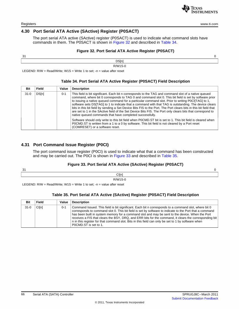
Registers www.ti.com
4.30 Port Serial ATA Active (SActive) Register (P0SACT)
The port serial ATA active (SActive) register (P0SACT) is used to indicate what command slots havecommands in them. The P0SACT is shown in Figure 32 and described in Table 34.
Figure 32. Port Serial ATA Active Register (P0SACT)31 0
DS[n]
R/W1S-0
LEGEND: R/W = Read/Write; W1S = Write 1 to set; -n = value after reset
Table 34. Port Serial ATA Active Register (P0SACT) Field Description
Bit Field Value Description
31-0 DS[n] 0-1 This field is bit significant. Each bit n corresponds to the TAG and command slot of a native queuedcommand, where bit 0 corresponds to TAG 0 and command slot 0. This bit field is set by software priorto issuing a native queued command for a particular command slot. Prior to writing P0CI[TAG] to 1,software sets DS[TAG] to 1 to indicate that a command with that TAG is outstanding. The device clearsbits in this bit field by sending a Set Device Bits FIS to the Port. The Port clears bits in this bit field thatare set to 1 in the SActive field of the Set Device Bits FIS. The Port only clears bits that correspond tonative queued commands that have completed successfully.
Software should only write to this bit field when P0CMD.ST bit is set to 1. This bit field is cleared whenP0CMD.ST is written from a 1 to a 0 by software. This bit field is not cleared by a Port reset(COMRESET) or a software reset.
4.31 Port Command Issue Register (P0CI)
The port command issue register (P0CI) is used to indicate what that a command has been constructedand may be carried out. The P0CI is shown in Figure 33 and described in Table 35.
Figure 33. Port Serial ATA Active (SActive) Register (P0SACT)31 0
CI[n]
R/W1S-0
LEGEND: R/W = Read/Write; W1S = Write 1 to set; -n = value after reset
Table 35. Port Serial ATA Active (SActive) Register (P0SACT) Field Description
Bit Field Value Description
31-0 CI[n] 0-1 Command Issued. This field is bit significant. Each bit n corresponds to a command slot, where bit 0corresponds to command slot 0. This bit field is set by software to indicate to the Port that a commandhas been built in system memory for a command slot and may be sent to the device. When the Portreceives a FIS that clears the BSY, DRQ, and ERR bits for the command, it clears the corresponding bitn in this register for that command slot. Bits in this field can only be set to 1 by software whenP0CMD.ST is set to 1.
66 Serial ATA (SATA) Controller SPRUGJ8C–March 2011Submit Documentation Feedback
© 2011, Texas Instruments Incorporated

www.ti.com Registers
4.32 Port Serial ATA Notification Register (P0SNTF)
The port serial ATA notification register (POSNTF) is used to determine if asynchronous notificationevents have occurred for directly connected devices and devices connected to a Port Multiplier. ThePOSNTF is shown in Figure 34 and described in Table 36.
Figure 34. Port Serial ATA Notification Register (POSNTF)31 16
Reserved
R-0
15 0
PMN[n]
R/W1C-0
LEGEND: R/W = Read/Write; R = Read only; W1C = Write 1 to clear; -n = value after reset
Table 36. Port Serial ATA Notification Register (POSNTF) Field Description
Bit Field Value Description
31-16 Reserved 0 Reserved.
15-0 PMN[n] 0-1 PM Notify. Indicates whether a particular device with the corresponding PM Port number issued aSet Device Bits FIS to the SATASS Port with the Notification bit set. Individual bits are cleared bysoftware writing 1s to the corresponding bit n positions. This bit field is reset on Global reset, but itis not reset by Port reset (COMRESET) or software reset.
• PM Port 0 sets bit 0• PM Port 0 sets bit 1
67SPRUGJ8C–March 2011 Serial ATA (SATA) ControllerSubmit Documentation Feedback
© 2011, Texas Instruments Incorporated

Registers www.ti.com
4.33 Port DMA Control Register (P0DMACR)
The port DMA control register (P0DMACR) contains bits for controlling the Port DMA engine. The softwarecan change the fields of this register only when P0CMD.ST=0. Power-up (system reset), Global reset, orPort reset (COMRESET) reset this register to the default value. The P0DMACR is shown in Figure 35 anddescribed in Table 37.
Figure 35. Port DMA Control Register (P0DMACR)31 16
Reserved
R-0
15 12 11 8 7 4 3 0
RXABL TXABL RXTS TXTS
R-0 R/W-0 R/W-4h R/W-4h
LEGEND: R/W = Read/Write; R = Read only; -n = value after reset
Table 37. Port DMA Control Register (P0DMACR) Field Description
Bit Field Value Description
31-16 Reserved 0 Reserved.
15-12 RXABL 0-Fh Receive Burst Limit. Allows software to limit the VBUSP master write burst size. This bit field isread/write when P0CMD.ST = 0 and read-only when P0CMD.ST = 1.
Note: SATASS master breaks the burst at 1Kbyte address boundaries regardless of the RXABL value.
0 Limit VBUSP burst size to 256 DWORDS
1h Limit VBUSP Burst size to 1 DWORD
2h Limit VBUSP Burst size to 2 DWORDs
3h Limit VBUSP Burst size to 4 DWORDs
4h Limit VBUSP Burst size to 8 DWORDs
5h Limit VBUSP Burst size to 16 DWORDs
6h Limit VBUSP Burst size to 32 DWORDs
7h Limit VBUSP Burst size to 64 DWORDs
8h Limit VBUSP Burst size to 128 DWORDs
9h-Fh Limit VBUSP burst size to 256 DWORDS
11-8 TXABL 0-Fh Transmit Burst Limit. This field allows software to limit the VBUSP master read burst size. This bit fieldis read/write when P0CMD.ST = 0 and read-only when P0CMD.ST = 1.
Note: SATASS master breaks the burst at 1Kbyte address boundaries regardless of the TXABL value.
0 Limit VBUSP burst size to 256 DWORDS
1h Limit VBUSP Burst size to 1 DWORD
2h Limit VBUSP Burst size to 2 DWORDs
3h Limit VBUSP Burst size to 4 DWORDs
4h Limit VBUSP Burst size to 8 DWORDs
5h Limit VBUSP Burst size to 16 DWORDs
6h Limit VBUSP Burst size to 32 DWORDs
7h Limit VBUSP Burst size to 64 DWORDs
8h Limit VBUSP Burst size to 128 DWORDs
9h-Fh Limit VBUSP burst size to 256 DWORDS
68 Serial ATA (SATA) Controller SPRUGJ8C–March 2011Submit Documentation Feedback
© 2011, Texas Instruments Incorporated

www.ti.com Registers
Table 37. Port DMA Control Register (P0DMACR) Field Description (continued)
Bit Field Value Description
7-4 RXTS 0-Fh Receive Transaction Size (RX_TRANSACTION_SIZE). This field defines the Port DMA transaction sizein DWORDs for receive (system bus write, device read) operation. This bit field is read/write whenP0CMD.ST = 0 and read-only when P0CMD.ST = 1. The maximum value of this bit field is determinedby the Rx FIFO Depth (P0_RXFIFO_DEPTH). If software attempts to write a value exceeding thismaximum value, the maximum value would be set instead.
0 1 DWORD
1h 2 DWORDs
2h 4 DWORDs
3h 8 DWORDs
4h 16 DWORDS (maximum value if P0_RXFIFO_DEPTH = 64)
5h 32 DWORDs
6h 64 DWORDs (maximum value if P0_RXFIFO_DEPTH = 128)
7h 128 DWORDs (maximum value if P0_RXFIFO_DEPTH = 256)
8h 256 DWORDs (maximum value if P0_RXFIFO_DEPTH = 512)
9h 512 DWORDs (maximum value if P0_RXFIFO_DEPTH = 1024)
Ah 1024 DWORDs (maximum value if P0_RXFIFO_DEPTH = 2048)
Bh-Fh Reserved
3-0 TXTS 0-Fh Transmit Transaction Size (TX_TRANSACTION_SIZE). This field defines the DMA transaction size inDWORDs for transmit (system bus read, device write) operation. This bit field is read/write whenP0CMD.ST = 0 and read-only when P0CMD.ST = 1. The maximum value of this bit field is determinedby the Tx FIFO Depth (P0_TXFIFO_DEPTH). If software attempts to write a value exceeding thismaximum value, the maximum value would be set instead.
0 1 DWORD
1h 2 DWORDs
2h 4 DWORDs
3h 8 DWORDs
4h 16 DWORDS (maximum value if P0_TXFIFO_DEPTH = 32)
5h 32 DWORDs (maximum value if P0_TXFIFO_DEPTH = 64)
6h 64 DWORDs (maximum value if P0_TXFIFO_DEPTH = 128)
7h 128 DWORDs (maximum value if P0_TXFIFO_DEPTH = 256)
8h 256 DWORDs (maximum value if P0_TXFIFO_DEPTH = 512)
9h 512 DWORDs (maximum value if P0_TXFIFO_DEPTH = 1024)
Ah 1024 DWORDs (maximum value if P0_TXFIFO_DEPTH = 2048)
Bh-Fh Reserved
69SPRUGJ8C–March 2011 Serial ATA (SATA) ControllerSubmit Documentation Feedback
© 2011, Texas Instruments Incorporated

Registers www.ti.com
4.34 Port PHY Control Register (P0PHYCR)
The port PHY control register (P0PHYCR) is used to control the PHY. These ports are configured for theWIZ6C2B2N5W0M (Maverick B2) macro. Refer to that spec for further details.
Note: This description is only valid for configuration GS60. See the corresponding P0PHYSR Registerdescription for each configuration. The P0PHYCR is shown in Figure 36 and described in Table 38.
Figure 36. Port PHY Control Register (P0PHYCR)31 30 29 26 25 24
ENPLL OVERRIDE Reserved TXDE
R/W-0 R/W-0 R-0 R/W-0
23 22 21 19 18 17 16
TXDE TXSWING TXCM TXINVPAIR RXEQ
R/W-0 R/W-0 R/W-0 R/W-0 R/W-0
15 13 12 10 9 8
RXEQ RXCDR RXTERM
R/W-0 R/W-0 R/W-0
7 6 5 4 3 0
RXINVPAIR LOS LB MPY
R/W-0 R/W-0 R/W-0 R/W-0
LEGEND: R/W = Read/Write; R = Read only; -n = value after reset
Table 38. Port PHY Control Register (P0PHYCR) Field Descriptions
Bit Field Value Description
31 ENPLL Enable Phy PLL. This must be enabled by software before initialization is started on the device.This bit should not be enabled unless the MPY field has been previously set or is being set in thesame write. Changing the MPY field while the PLL is enabled disrupts the link clocks and maydisrupt the link, requiring a port reset to fix. The PLL may be turned off while the link is in alow-power state (Partial or Slumber). If it is, then it must be re-enabled ~1us + 200 refclock cyclesbefore software attempts to remove the low power state.
CAUTION
If the PLL is disabled in a low-power state, theSATASS cannot wake up from low power based ona device request. If the device requests wakeup andthe SATASS does not respond, a port reset may berequired after software re-enables the PLL andremoves the low-power state. Caution should betaken to never disable the PLL if it is possible thatthe device will request a wake up from low power.
0 Phy PLL is disabled.
1 Phy PLL is enabled.
70 Serial ATA (SATA) Controller SPRUGJ8C–March 2011Submit Documentation Feedback
© 2011, Texas Instruments Incorporated

www.ti.com Registers
Table 38. Port PHY Control Register (P0PHYCR) Field Descriptions (continued)
Bit Field Value Description
30 OVERRIDE Override for Clock Stopping. Normally the functional clock can only be stopped if the link is put intoPartial or Slumber power mode. However, if there is no device attached (such as in a removablemedia situation) you may wish to stop the functional clocks but not be able to enter a low-powerstate. In this case, software can set the OVERRIDE bit to 1, removing the requirement for alow-power state.
CAUTION
When there is a device attached and the OVERRIDEbit is used, if the functional clock is stopped whenthe link is not in a low-power state may ruin the linkand cause undetermined behavior. A port reset orfull SATASS reset may be required to recover.
0 Normal
1 Override
29-26 Reserved 0 Reserved.
25-22 TXDE 0-Fh Transmitter De-Emphasis. Selects 1 of 16 output de-emphasis settings from 0 to 71.42%
Reduction
% dB
0 0 0
1 4.76 -0.42
2h 9.52 -0.87
3h 14.28 -1.34
4h 19.04 -1.83
5h 23.8 -2.36
6h 28.56 -2.92
7h 33.32 -3.52
8h 38.08 -4.16
9h 42.85 -4.86
Ah 47.61 -5.61
Bh 52.38 -6.44
Ch 57.14 -7.35
Dh 61.9 -8.38
Eh 66.66 -9.54
Fh 71.42 -10.87
21-19 TXSWING 0-7h Transmitter Output Swing. Selects 1 of 8 output amplitude settings between 125 and 1375 mV(dfpp).
0 125
1h 250
2h 500
3h 625
4h 750
5h 1000
6h 1250
7h 1375
18 TXCM Transmitter Common Mode. Adjusts the common mode to suit the termination at the attachedreceiver.
0 Normal Common Mode
1 Raised common mode. Common mode raised by 5% of e54.
71SPRUGJ8C–March 2011 Serial ATA (SATA) ControllerSubmit Documentation Feedback
© 2011, Texas Instruments Incorporated

Registers www.ti.com
Table 38. Port PHY Control Register (P0PHYCR) Field Descriptions (continued)
Bit Field Value Description
17 TXINVPAIR Transmitter Invert Polarity. Inverts the polarity of TXP0 and TXN
16-13 RXEQ 0-Fh Receiver Equalizer. Enables and configures the adaptive equalizer to compensate for loss in thetransmission media.
Low FrequencyGain Zero Frequency
0 Maximum —
1h Adaptive
2h-7h Reserved
8h Adaptive 365 MHz
9h Adaptive 275 MHz
Ah Adaptive 195 MHz
Bh Adaptive 140 MHz
Ch Adaptive 105 MHz
Dh Adaptive 75 MHz
Eh Adaptive 55 MHz
Fh Adaptive 50 MHz
12-10 RXCDR 0-7h Receiver Clock/data Recovery. Configures the clock/data recovery algorithm.
0 First order, threshold of 1. Phase offset tracking up to ±312 ppm. Suitable for use in asynchronoussystems with low frequency offset.
1h First order, threshold of 16. Phase offset tracking up to ±260 ppm in the presence of ..10101010..training pattern, or ±195 ppm in the presence of 27 PRBS. Suitable for use in synchronous systems.Offers superior rejection of random jitter, but is less responsive to systematic variation such assinusoidal jitter.
2h Second order, high precision, threshold of 1. Highest precision frequency offset matching butrelatively poor response to changes in frequency offset, and long lock time. Suitable for use insystems with fixed frequency offset.
3h Second order, high precision, threshold of 16. Highest precision frequency offset matching butpoorest response to changes in frequency offset, and longest lock time. Suitable for use in systemswith fixed frequency offset and low systematic variation.
4h Second order, low precision, threshold of 1. Best response to changes in frequency offset andfastest lock time, but lowest precision frequency offset matching. Suitable for use in systems withspread spectrum clocking.
5h Second order, low precision, threshold of 16. Good response to changes in frequency offset andfast lock time, but low precision frequency offset matching. Suitable for use in systems with spreadspectrum clocking.
6h First order, threshold of 1 with fast lock. Phase offset tracking up to ±1560 ppm in the presence of..10101010.. training pattern; and ±312 ppm, otherwise.
7h Second order, low precision with fast lock. As per setting 100, but with improved response tochanges in frequency offset when not close to lock.
9-8 RXTERM 0-3h Receiver Termination. Selects input termination options suitable for a variety of AC or DC coupledscenarios.
0 Common point set to VSSA. This configuration is for applications that are AC coupled at the receiveend that require a 0V common mode. Common mode termination is direct to VSSA.
1h Common point set to 0.8 VDDA. This configuration is for AC coupled systems. The transmitter has noeffect on the receiver common mode, which is set to optimize the input sensitivity of the receiver.Common mode termination is via a 50 pF capacitor to VSSA. This mode is probably not used forSATA.
2h Common point set to 0.2 VDDA. This configuration is for applications (DC coupled or AC coupled atthe transmit end) that require a low common mode. Common mode termination is via a 50 pFcapacitor to VSSA.
3h Common point floating, wide common mode range. This configuration utilizes the internal ACcoupled level shifters to support a wide common mode range, and it therefore requires DCbalanced coding. It can also be used to achieve high single ended impedance. This mode isprobably not used for SATA.
7 RXINVPAIR 0-1 Receiver Invert Polarity. Inverts the polarity of RXP0 and RXN.
72 Serial ATA (SATA) Controller SPRUGJ8C–March 2011Submit Documentation Feedback
© 2011, Texas Instruments Incorporated
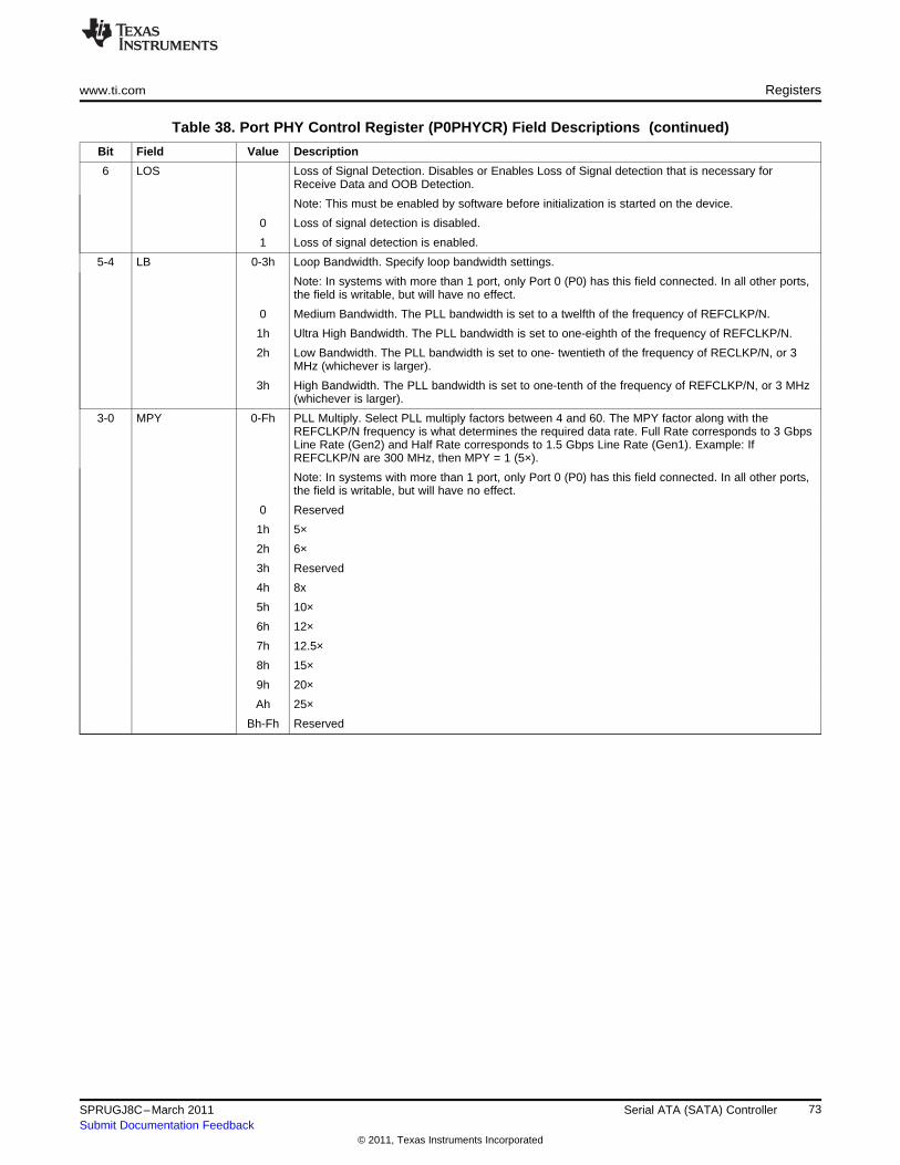
www.ti.com Registers
Table 38. Port PHY Control Register (P0PHYCR) Field Descriptions (continued)
Bit Field Value Description
6 LOS Loss of Signal Detection. Disables or Enables Loss of Signal detection that is necessary forReceive Data and OOB Detection.
Note: This must be enabled by software before initialization is started on the device.
0 Loss of signal detection is disabled.
1 Loss of signal detection is enabled.
5-4 LB 0-3h Loop Bandwidth. Specify loop bandwidth settings.
Note: In systems with more than 1 port, only Port 0 (P0) has this field connected. In all other ports,the field is writable, but will have no effect.
0 Medium Bandwidth. The PLL bandwidth is set to a twelfth of the frequency of REFCLKP/N.
1h Ultra High Bandwidth. The PLL bandwidth is set to one-eighth of the frequency of REFCLKP/N.
2h Low Bandwidth. The PLL bandwidth is set to one- twentieth of the frequency of RECLKP/N, or 3MHz (whichever is larger).
3h High Bandwidth. The PLL bandwidth is set to one-tenth of the frequency of REFCLKP/N, or 3 MHz(whichever is larger).
3-0 MPY 0-Fh PLL Multiply. Select PLL multiply factors between 4 and 60. The MPY factor along with theREFCLKP/N frequency is what determines the required data rate. Full Rate corresponds to 3 GbpsLine Rate (Gen2) and Half Rate corresponds to 1.5 Gbps Line Rate (Gen1). Example: IfREFCLKP/N are 300 MHz, then MPY = 1 (5×).
Note: In systems with more than 1 port, only Port 0 (P0) has this field connected. In all other ports,the field is writable, but will have no effect.
0 Reserved
1h 5×
2h 6×
3h Reserved
4h 8x
5h 10×
6h 12×
7h 12.5×
8h 15×
9h 20×
Ah 25×
Bh-Fh Reserved
73SPRUGJ8C–March 2011 Serial ATA (SATA) ControllerSubmit Documentation Feedback
© 2011, Texas Instruments Incorporated
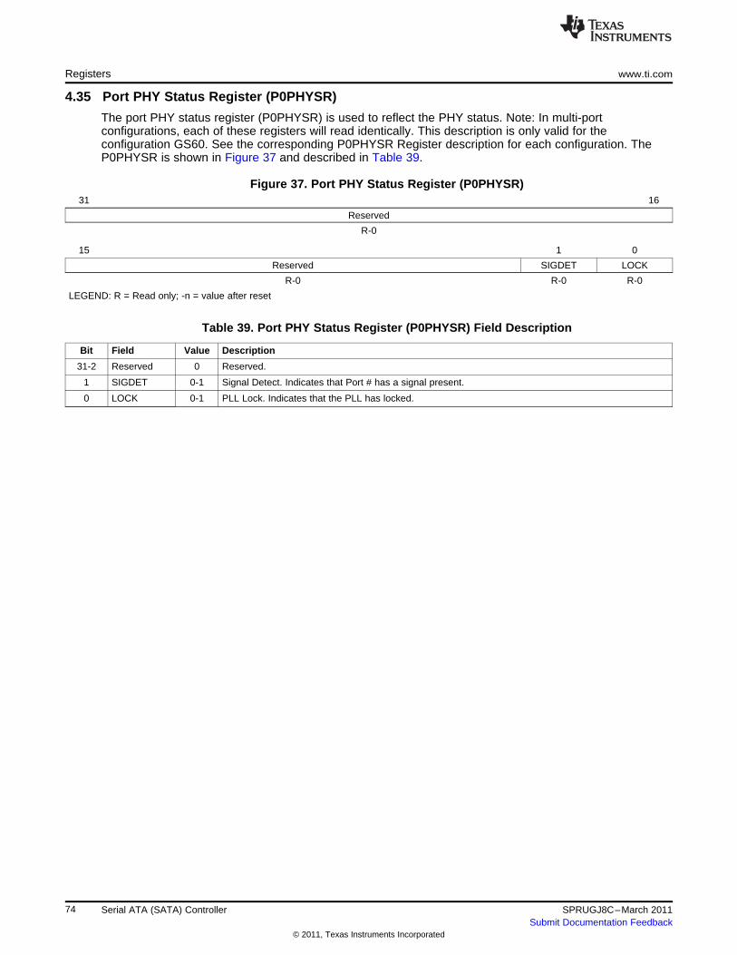
Registers www.ti.com
4.35 Port PHY Status Register (P0PHYSR)
The port PHY status register (P0PHYSR) is used to reflect the PHY status. Note: In multi-portconfigurations, each of these registers will read identically. This description is only valid for theconfiguration GS60. See the corresponding P0PHYSR Register description for each configuration. TheP0PHYSR is shown in Figure 37 and described in Table 39.
Figure 37. Port PHY Status Register (P0PHYSR)31 16
Reserved
R-0
15 1 0
Reserved SIGDET LOCK
R-0 R-0 R-0
LEGEND: R = Read only; -n = value after reset
Table 39. Port PHY Status Register (P0PHYSR) Field Description
Bit Field Value Description
31-2 Reserved 0 Reserved.
1 SIGDET 0-1 Signal Detect. Indicates that Port # has a signal present.
0 LOCK 0-1 PLL Lock. Indicates that the PLL has locked.
74 Serial ATA (SATA) Controller SPRUGJ8C–March 2011Submit Documentation Feedback
© 2011, Texas Instruments Incorporated

www.ti.com
Appendix A Revision History
Table 40 lists the changes made since the previous version of this document.
Table 40. Document Revision History
Reference Additions/Modifications/Deletions
Figure 16 Changed reset value of PHY_CTRL bit.
Table 18 Changed Value of PHY_CTRL bit.
75SPRUGJ8C–March 2011 Revision HistorySubmit Documentation Feedback
© 2011, Texas Instruments Incorporated

IMPORTANT NOTICE
Texas Instruments Incorporated and its subsidiaries (TI) reserve the right to make corrections, modifications, enhancements, improvements,and other changes to its products and services at any time and to discontinue any product or service without notice. Customers shouldobtain the latest relevant information before placing orders and should verify that such information is current and complete. All products aresold subject to TI’s terms and conditions of sale supplied at the time of order acknowledgment.
TI warrants performance of its hardware products to the specifications applicable at the time of sale in accordance with TI’s standardwarranty. Testing and other quality control techniques are used to the extent TI deems necessary to support this warranty. Except wheremandated by government requirements, testing of all parameters of each product is not necessarily performed.
TI assumes no liability for applications assistance or customer product design. Customers are responsible for their products andapplications using TI components. To minimize the risks associated with customer products and applications, customers should provideadequate design and operating safeguards.
TI does not warrant or represent that any license, either express or implied, is granted under any TI patent right, copyright, mask work right,or other TI intellectual property right relating to any combination, machine, or process in which TI products or services are used. Informationpublished by TI regarding third-party products or services does not constitute a license from TI to use such products or services or awarranty or endorsement thereof. Use of such information may require a license from a third party under the patents or other intellectualproperty of the third party, or a license from TI under the patents or other intellectual property of TI.
Reproduction of TI information in TI data books or data sheets is permissible only if reproduction is without alteration and is accompaniedby all associated warranties, conditions, limitations, and notices. Reproduction of this information with alteration is an unfair and deceptivebusiness practice. TI is not responsible or liable for such altered documentation. Information of third parties may be subject to additionalrestrictions.
Resale of TI products or services with statements different from or beyond the parameters stated by TI for that product or service voids allexpress and any implied warranties for the associated TI product or service and is an unfair and deceptive business practice. TI is notresponsible or liable for any such statements.
TI products are not authorized for use in safety-critical applications (such as life support) where a failure of the TI product would reasonablybe expected to cause severe personal injury or death, unless officers of the parties have executed an agreement specifically governingsuch use. Buyers represent that they have all necessary expertise in the safety and regulatory ramifications of their applications, andacknowledge and agree that they are solely responsible for all legal, regulatory and safety-related requirements concerning their productsand any use of TI products in such safety-critical applications, notwithstanding any applications-related information or support that may beprovided by TI. Further, Buyers must fully indemnify TI and its representatives against any damages arising out of the use of TI products insuch safety-critical applications.
TI products are neither designed nor intended for use in military/aerospace applications or environments unless the TI products arespecifically designated by TI as military-grade or "enhanced plastic." Only products designated by TI as military-grade meet militaryspecifications. Buyers acknowledge and agree that any such use of TI products which TI has not designated as military-grade is solely atthe Buyer's risk, and that they are solely responsible for compliance with all legal and regulatory requirements in connection with such use.
TI products are neither designed nor intended for use in automotive applications or environments unless the specific TI products aredesignated by TI as compliant with ISO/TS 16949 requirements. Buyers acknowledge and agree that, if they use any non-designatedproducts in automotive applications, TI will not be responsible for any failure to meet such requirements.
Following are URLs where you can obtain information on other Texas Instruments products and application solutions:
Products Applications
Audio www.ti.com/audio Communications and Telecom www.ti.com/communications
Amplifiers amplifier.ti.com Computers and Peripherals www.ti.com/computers
Data Converters dataconverter.ti.com Consumer Electronics www.ti.com/consumer-apps
DLP® Products www.dlp.com Energy and Lighting www.ti.com/energy
DSP dsp.ti.com Industrial www.ti.com/industrial
Clocks and Timers www.ti.com/clocks Medical www.ti.com/medical
Interface interface.ti.com Security www.ti.com/security
Logic logic.ti.com Space, Avionics and Defense www.ti.com/space-avionics-defense
Power Mgmt power.ti.com Transportation and www.ti.com/automotiveAutomotive
Microcontrollers microcontroller.ti.com Video and Imaging www.ti.com/video
RFID www.ti-rfid.com Wireless www.ti.com/wireless-apps
RF/IF and ZigBee® Solutions www.ti.com/lprf
TI E2E Community Home Page e2e.ti.com
Mailing Address: Texas Instruments, Post Office Box 655303, Dallas, Texas 75265Copyright © 2011, Texas Instruments Incorporated