serial ata international organization - sata-io
TRANSCRIPT
Tektronix, Inc.
SATA Test Procedures Revision 1.4 ver 1.0 1 Page 1
Serial ATA International Organization
Version 1.0 20-August-2009
Serial ATA Interoperability Program Revision 1.4 Tektronix Test Procedures for PHY, TSG and OOB Tests (Real-Time DSO measurements for Hosts and Devices) This document is provided "AS IS" and without any warranty of any kind, including, without limitation, any express or implied warranty of non-infringement, merchantability or fitness for a particular purpose. In no event shall SATA-IO or any member of SATA-IO be liable for any direct, indirect, special, exemplary, punitive, or consequential damages, including, without limitation, lost profits, even if advised of the possibility of such damages. This material is provided for reference only. The Serial ATA International Organization does not endorse the vendor equipment outlined in this document.
Tektronix, Inc.
TABLE OF CONTENTS
TABLE OF CONTENTS.........................................................................................2
INTRODUCTION ...................................................................................................8 EQUIPMENT PREPARATION ........................................................................................................ 8
PHY GENERAL REQUIREMENTS (PHY 1-4) ..................................................9 TEST PHY-01 - UNIT INTERVAL............................................................................................... 10 TEST PHY-02 - FREQUENCY LONG TERM STABILITY .............................................................. 15 TEST PHY-03 - SPREAD-SPECTRUM MODULATION FREQUENCY............................................. 20 TEST PHY-04 - SPREAD-SPECTRUM MODULATION DEVIATION.............................................. 24
PHY TRANSMITTED SIGNAL REQUIREMENTS (TSG 1-16) ....................28 TEST TSG-01 - DIFFERENTIAL OUTPUT VOLTAGE................................................................... 29 TEST TSG-02 - RISE/FALL TIME ............................................................................................. 33 TEST TSG-03 - DIFFERENTIAL SKEW...................................................................................... 36 TEST TSG-04 - AC COMMON MODE VOLTAGE ....................................................................... 40 TEST TSG-05 - RISE/FALL IMBALANCE (OBSOLETE) .............................................................. 43 TEST TSG-06 - AMPLITUDE IMBALANCE (OBSOLETE) ............................................................ 47 TEST TSG-07 - TJ AT CONNECTOR, CLOCK TO DATA, FBAUD/10 (OBSOLETE) ...................... 51 TEST TSG-08 - DJ AT CONNECTOR, CLOCK TO DATA, F /10 (OBSOLETE) ......................... 56 BAUD
TEST TSG-09 - GEN1 (1.5 GB/S) TJ AT CONNECTOR, CLOCK TO DATA, FBAUD/500 ............. 60 TEST TSG-10 - GEN1 (1.5 GB/S) DJ AT CONNECTOR, CLOCK TO DATA, F /500 ................ 65 BAUD
TEST TSG-11 - GEN2 (3GB/S) TJ AT CONNECTOR, CLOCK TO DATA, F /500..................... 69 BAUD
TEST TSG-12 - GEN2 (3GB/S) DJ AT CONNECTOR, CLOCK TO DATA, F /500 .................... 74 BAUD
TEST TSG-13 - TRANSMIT JITTER ........................................................................................... 79 TEST TSG-14: - TX MAXIMUM DIFFERENTIAL OUTPUT VOLTAGE AMPLITUDE (GEN3I) ........ 86 TEST TSG-15: - TX MINIMUM DIFFERENTIAL OUTPUT VOLTAGE AMPLITUDE (GEN3I).......... 89 TEST TSG-16 - TX AC COMMON MODE VOLTAGE (GEN3I) ................................................... 94
PHY OOB REQUIREMENTS (OOB 1-7) ..........................................................97 TEST OOB-01 – OOB SIGNAL DETECTION THRESHOLD......................................................... 98 TEST OOB-02 – UI DURING OOB SIGNALING...................................................................... 101 TEST OOB-03 – COMINIT/RESET AND COMWAKE TRANSMIT BURST LENGTH ............. 101 TEST OOB-04 – COMINIT/RESET TRANSMIT GAP LENGTH .............................................. 101 TEST OOB-05 – COMWAKE TRANSMIT GAP LENGTH........................................................ 101 TEST OOB-06 – COMWAKE GAP DETECTION WINDOWS................................................... 106 TEST OOB-07 – COMINIT GAP DETECTION WINDOWS ...................................................... 110
APPENDIX A – RESOURCE REQUIREMENTS...........................................114
APPENDIX B – TEST SETUPS.........................................................................116 TRANSMITTER DEVICE PUT TESTS USING BIST-FIS............................................................. 116 TRANSMITTER HOST PUT TESTS USING BIST-FIS ................................................................ 116 OUT-OF-BAND (OOB) DEVICE PUT TESTS USING AWG ....................................................... 117 OUT-OF-BAND (OOB) HOST PUT TESTS USING AWG........................................................... 118 FIGURE 4 TESTS USING AWG ................................................................................................ 119
SATA Test Procedures Revision 1.4 ver 1.0 2 Page 2
Tektronix, Inc.
APPENDIX C – OOB SETUP PROCEDURES................................................120
APPENDIX D – REAL-TIME DSO MEASUREMENT ACCURACY .........121
APPENDIX E – RETURN LOSS VERIFICATION PROCEDURE..............122
APPENDIX F – OOB-01 LEVEL CALIBRATION PROCEDURE FOR AWG7102 ..............................................................................................................131
APPENDIX G – CALIBRATION AND VERIFICATION OF JITTER MEASUREMENT DEVICES.............................................................................136
APPENDIX H – CONVERSION OF DBM TO DBMV...................................143
SATA Test Procedures Revision 1.4 ver 1.0 3 Page 3

Tektronix, Inc.
MODIFICATION RECORD January 16, 2006 (Version 1.0) INITIAL RELEASE, TO LOGO TF MOI GROUP
Andy Baldman: Initial Template Release
February 2, 2006 (Tektronix Version .9 - beta) INITIAL RELEASE Kees Propstra, John Calvin, Mike Martin: Phy and TSG MOI Contributions Eugene Mayevskiy: Tx/Rx Phy MOI Contributions
February 8, 2006 (Tektronix Version .91 - beta) Kees Propstra, John Calvin, Mike Martin: Phy and TSG MOI Contributions Eugene Mayevskiy: Tx/Rx Phy MOI Contributions
February 11, 2006 (Tektronix Version .92 RC) Eugene Mayevskiy: SI01-SI09 Phy MOI Contributions John Calvin: OOB1-OOB7 MOI Contributions.
February 24, 2006 (Tektronix Version .93 RC) Kees Propstra: updated Phy02, TSG01-12 Updated Appendix A Updated Appendix C: long term freq stability, rise fall and amplitude imbalance, differential skew msmt
March 1, 2006 (Tektronix Version .94 RC) Mike Martin: updated OOB Test Documentation. Minor formatting changes throughout document.
March 31, 2006 (Tektronix Version .95 RC) Mike Martin: incorporated reviewer’s feedback
April 12, 2006 (Tektronix Version .96 RC) Eugene Mayevskiy: incorporated reviewer’s feedback (group 2, 4, 6, Appendix E) Kees Propstra: incorporated reviewers’ feedback (group 1, 3, 5, Appendix A)
May 17, 2006 (Tektronix Version .97 RC) Eugene Mayevskiy, Mike Martin, Kees Propstra, John Calvin Incorporated changes to track the IW 1.0 Unified test specification as well as reviewers comments. Added Appendix F for Equivalent Time/ TDNA accuracy parameters Added Appendix G for Real Time accuracy parameters.
May 25, 2006 (Tektronix Version .98 RC-2) John Calvin
Incorporated reviewer feedback and broke document into two separate document which separate the RT centric measurements from the ET based ones
May 31, 2006 (Tektronix Version .98 RC-4) Mike Martin
Incorporated reviewer feedback from SATA Logo conference call review: PHY-02: Cleaned up corrupted text – removed bullets 1-4 and associated text. PHY-04: Corrected test name in discussion section. Corrected deviation formula to show ppm. All TSG tests: for each test that uses LBP, added directions to inspect waveform for proper disparity. TSG-02: removed reference to LFTP. Removed reference to “m” and “x” requirements. TSG-03: corrected wording on calculation to include average of the absolute values of the mean for skew1 and skew2. Removed reference to “m” and “x” requirements. OOB-1: Rewrote test to reflect latest changes in Unified Test Document. OOB-6: Corrected statement to read “upper limit”, rather than “lower limit” OOB-7: Corrected statement to read “upper limit”, rather than “lower limit” Appendix B: Corrected image corruption and duplicate images. Appendix C, Section 1: Added wording about using Scope Cursors rather than JIT3 Cursors for making long term frequency stability measurements. Appendix C, Section 9: Added more detailed information on making differential skew measurement setups.
SATA Test Procedures Revision 1.4 ver 1.0 4 Page 4
Tektronix, Inc.
July 25, 2006 (Tektronix Version .98 RC-5) Mike Martin
Incorporated reviewer feedback on Phy-02, Phy-03, Phy-04, TSG-01, TSG-02, TSG-03, and OOB-07 Broke up Appendix C, and distributed the text as “Detailed Procedure” in the appropriate test steps to improve readability. Added legal statement to cover
July 31, 2006 (Tektronix Version .98 RC-6) Mike Martin
Added Phy-02 content to show higher resolution readings.
August 03, 2006 (Tektronix Version 1.0RC) Mike Martin
No changes, just 1.0RC version number
September 18, 2006 (Tektronix Version 1.07) Mike Martin
Replaced DUT with PUT in all instances Added average measurement technique for PHY-02 and PHY-04 Added HOST changes
September 21, 2006 (Tektronix Version 1.08) Mike Martin
Rolled to 1.08 as a result of group review Minor text change to PHY-02 and PHY-04 (removed “mean” on µ line) Added Gen1 statement to Appendix D
September 30, 2006 (Tektronix Version 1.09) Mike Martin
Rolled to 1.09 as a result of group review Modified OOB tests to reflect use of AWG7102 generator
January 2. 2007 (Tektronix Revision 1.1, Version 0.91)
Mike Martin Rolled to new rev/ver numbering scheme Modified PHY-02 and PHY-04 to use period method Added Return Loss Verification Procedure
January 16. 2007 (Tektronix Revision 1.1, Version 0.92)
Mike Martin Modified TSG-06 to show explicit method for measuring mode, and 2nd bit on MFTP. Modified OOB-01, OOB-06, and OOB-07 to use 2ms record length. Modified all OOB tests to include Host procedures. Corrected cable part number 174-4944-00, and added required SW version numbers in Appendix A. Added Scope External Attenuator Setting to Return Loss Verification Procedure
January 23. 2007 (Tektronix Revision 1.1, Version 0.93) Mike Martin Modified PHY-01 to use JIT3 for enhanced test efficiency. Corrected formulas for PHY-02 and PHY-04 to get proper result polarity. Corrected wording on PHY-02 non-SSC to direct use of ref waveform for full resolution. Modified TSG-02 to use JIT3 for enhanced test efficiency. Corrected TSG-07 through TSG-10 to reflect UTD changes to test requirements. Corrected TSG-11 and TSG-12 to incorporate 2nd order PLL.
January 31. 2007 (Tektronix Revision 1.1, Version 0.94)
Mike Martin Corrected typo in TSG-09, three places where fBAUD/10 should have been fBAUD/500.
February 1. 2007 (Tektronix Revision 1.1, Version 1.0RC)
Mike Martin
SATA Test Procedures Revision 1.4 ver 1.0 5 Page 5
Tektronix, Inc.
Rolled version for release candidate.
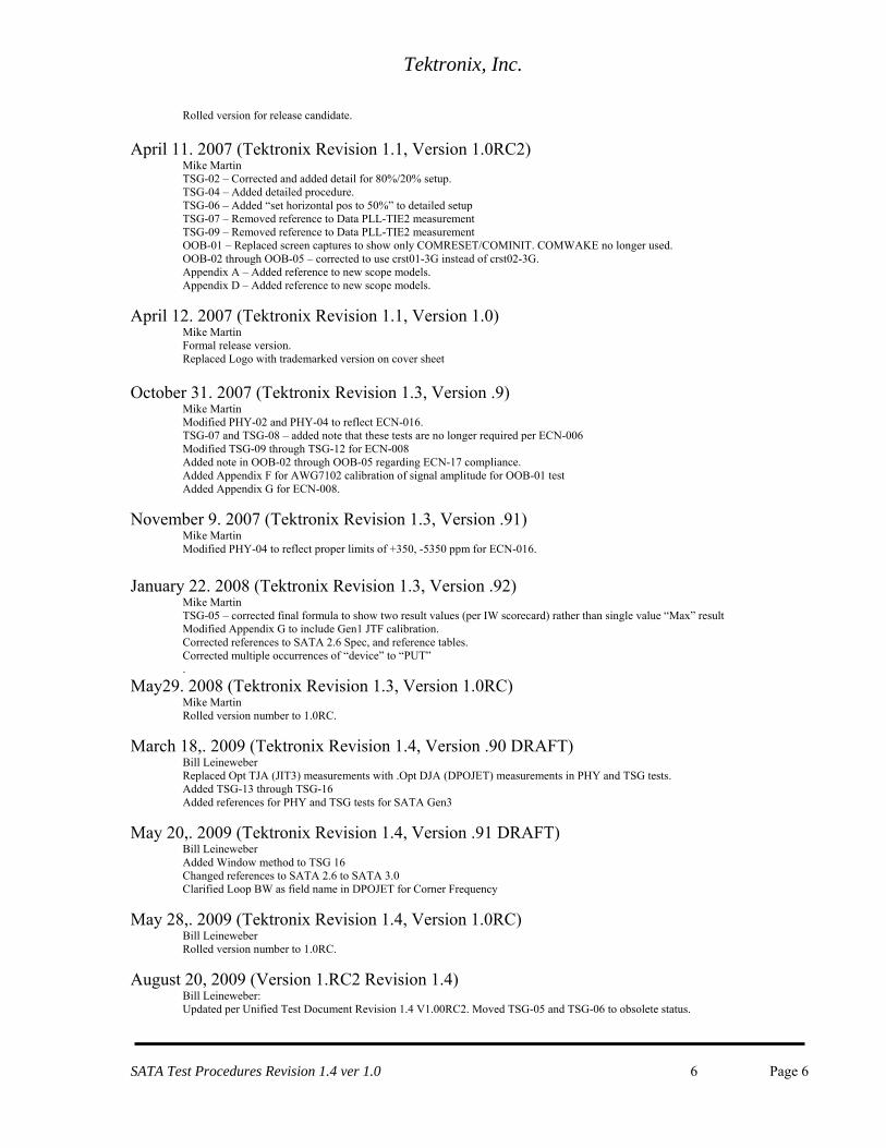
April 11. 2007 (Tektronix Revision 1.1, Version 1.0RC2)
Mike Martin TSG-02 – Corrected and added detail for 80%/20% setup. TSG-04 – Added detailed procedure. TSG-06 – Added “set horizontal pos to 50%” to detailed setup TSG-07 – Removed reference to Data PLL-TIE2 measurement TSG-09 – Removed reference to Data PLL-TIE2 measurement OOB-01 – Replaced screen captures to show only COMRESET/COMINIT. COMWAKE no longer used. OOB-02 through OOB-05 – corrected to use crst01-3G instead of crst02-3G. Appendix A – Added reference to new scope models. Appendix D – Added reference to new scope models.
April 12. 2007 (Tektronix Revision 1.1, Version 1.0) Mike Martin Formal release version. Replaced Logo with trademarked version on cover sheet
October 31. 2007 (Tektronix Revision 1.3, Version .9)
Mike Martin Modified PHY-02 and PHY-04 to reflect ECN-016. TSG-07 and TSG-08 – added note that these tests are no longer required per ECN-006 Modified TSG-09 through TSG-12 for ECN-008 Added note in OOB-02 through OOB-05 regarding ECN-17 compliance. Added Appendix F for AWG7102 calibration of signal amplitude for OOB-01 test Added Appendix G for ECN-008.
November 9. 2007 (Tektronix Revision 1.3, Version .91) Mike Martin Modified PHY-04 to reflect proper limits of +350, -5350 ppm for ECN-016.
January 22. 2008 (Tektronix Revision 1.3, Version .92)
Mike Martin TSG-05 – corrected final formula to show two result values (per IW scorecard) rather than single value “Max” result Modified Appendix G to include Gen1 JTF calibration. Corrected references to SATA 2.6 Spec, and reference tables. Corrected multiple occurrences of “device” to “PUT” .
May29. 2008 (Tektronix Revision 1.3, Version 1.0RC) Mike Martin Rolled version number to 1.0RC.
March 18,. 2009 (Tektronix Revision 1.4, Version .90 DRAFT) Bill Leineweber Replaced Opt TJA (JIT3) measurements with .Opt DJA (DPOJET) measurements in PHY and TSG tests. Added TSG-13 through TSG-16 Added references for PHY and TSG tests for SATA Gen3
May 20,. 2009 (Tektronix Revision 1.4, Version .91 DRAFT) Bill Leineweber Added Window method to TSG 16 Changed references to SATA 2.6 to SATA 3.0 Clarified Loop BW as field name in DPOJET for Corner Frequency
May 28,. 2009 (Tektronix Revision 1.4, Version 1.0RC) Bill Leineweber Rolled version number to 1.0RC.
August 20, 2009 (Version 1.RC2 Revision 1.4) Bill Leineweber: Updated per Unified Test Document Revision 1.4 V1.00RC2. Moved TSG-05 and TSG-06 to obsolete status.
SATA Test Procedures Revision 1.4 ver 1.0 6 Page 6
Tektronix, Inc.
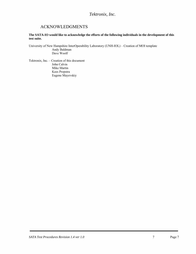
ACKNOWLEDGMENTS The SATA-IO would like to acknowledge the efforts of the following individuals in the development of this test suite. University of New Hampshire InterOperability Laboratory (UNH-IOL) – Creation of MOI template
Andy Baldman Dave Woolf
Tektronix, Inc. – Creation of this document John Calvin Mike Martin Kees Propstra Eugene Mayevskiy
SATA Test Procedures Revision 1.4 ver 1.0 7 Page 7
Tektronix, Inc.
INTRODUCTION The tests contained in this document are organized in order to simplify the identification of information related to a test, and to facilitate in the actual testing process. Tests are separated into groups, primarily in order to reduce setup time in the lab environment, however the different groups typically also tend to focus on specific aspects of device functionality. The test definitions themselves are intended to provide a high-level description of the motivation, resources, procedures, and methodologies specific to each test. Formally, each test description contains the following sections: Purpose
This document outlines precise and specific procedures required to conduct SATA IW UTD ver. 1.4 tests. This document covers the following tests which are all Tektronix Real Time DSO based. These tests can be run on either host or drive products.
Test Coverage
PHY GENERAL REQUIREMENTS (PHY 1-4) PHY TRANSMITTED SIGNAL REQUIREMENTS (TSG 1-16) PHY OOB REQUIREMENTS (OOB 1-7)
Equipment Preparation
Prior to making any measurements, the following steps must be taken to assure accurate measurements:
1. Allow a minimum of 20 minutes warm-up time for oscilloscope and AWG. 2. Run scope SPC calibration routine. It is necessary to remove all probes from the scope before running SPC. 3. If using probes, perform the probe calibration defined for the specific probes being used. 4. If using external attenuators to meet the SATA specification for Lab Load on the 50mV range of the scope, follow the procedure outlined in Appendix E. 5. Perform deskew to compensate for skew between measurement channels. Note that it is critical to select “Off” for the “Display Only” control on the Deskew setup window. This will assure that the deskew data is stored with any waveforms that are stored. 6. Refer to Appendix G to determine the appropriate JTF corner frequency for your measurement system. The Tektronix jitter and timing measurement applications use the JTF corner frequency as the ‘Loop BW’ parameter.
SATA Test Procedures Revision 1.4 ver 1.0 8 Page 8
Tektronix, Inc.
PHY GENERAL REQUIREMENTS (PHY 1-4) Overview:
This group of tests verifies the Phy General Requirements, as defined in Section 2.12 of the SATA Interoperability Unified Test Document, program revision 1.4 (which references the SATA Standard, v3.0).
SATA Test Procedures Revision 1.4 ver 1.0 9 Page 9
Tektronix, Inc.
Test PHY-01 - Unit Interval Purpose: To verify that the Unit Interval of the PUT’s transmitter is within the conformance limit. References:
[1] SATA Standard, 7.2.1, Table 7-1 – General Specifications [2] Ibid, 7.2.2.1.4 – Unit Interval [3] SATA Unified Test Document, UTD 1.4 [4] Ibid, 7.4.11 – SSC Profile
Resource Requirements: See Appendix A Discussion:
Reference [1] specifies the general PHY conformance limits for SATA PUTs. This specification includes conformance limits for the mean Unit Interval (UI). Reference [2] provides the definition of this term for the purposes of SATA testing. Reference [3] defines the measurement requirements for this test. In this test, the mean UI value measurement is based on the average of at least 100,000 observed UI’s, measured at the transmitter output. Test Setup: Connect equipment as shown in Appendix B, figure 1 or 2 as appropriate. Note that it is acceptable to use either differential or pseudo-differential (single ended plus math waveform) probes for these measurements. This test should be done with SSC ON if available. If the PUT does not support SSC, a measurement with SSC OFF is acceptable. Test Procedure: Using techniques and equipment as described in Appendix A of the SATA Pre-Test MOI, or equivalent, place the PUT in BISTFIS mode transmitting an HFTP pattern. Depending on the capability of the PUT, and the equipment available, it is acceptable to use either BIST-T or BIST-L to produce the needed test pattern. If the PUT supports disconnects, remove the SATA PRE-TEST system, and connect the SATA test fixture. Some PUTs require that the connection not be broken after BIST has been activated. In these situations, it may be necessary to use power splitters to allow simultaneous connection of the PRE-TEST system and the test equipment. Refer to Appendix A of the PRE-TEST MOI for additional details. Refer to Appendix G to use the appropriate JTF corner frequency for your measurement system. The Tektronix jitter and timing measurement applications use the JTF corner frequency as the ‘Loop BW’ parameter. Start the Jitter and Analysis (DPOJET) application on the oscilloscope by selecting it from the Analysis pull down menu. Recall the appropriate setup:
Gen1: SATA_PHY01_G1.set Gen2: SATA_PHY01_G2.set Gen3: SATA_PHY01_G3.set
See the detailed procedure which follows. This test is performed at all data rates for SATA PUTs. Test pattern(s): SATA usage model:
SATA Test Procedures Revision 1.4 ver 1.0 10 Page 10
Tektronix, Inc.
HFTP 1.5 Gbps, 3.0 Gbps (Gen1i/m and Gen2i/m respectively), and 6.0 Gbps.
Gen1: 10 us/div, 50 ps/pt (> 100,000 UI) Gen2: 4 us/div, 25 ps/pt (> 100,000 UI) Gen3: 2 us/div, 25 ps/pt (> 100,000 UI) Horizontal scale settings and Record Lengths vary between oscilloscope models, so select the settings that are closest to those specified in this procedure. Observable Results:
The mean Unit Interval value shall be between 666.4333 ps and 670.2333 ps for 1.5 Gbps PUTs, between 333.2167ps, 335.1167ps for 3.0 Gbps, and between 166.6083, 167.5583 for 6.0 Gbps PUTs.
Detailed Procedure:
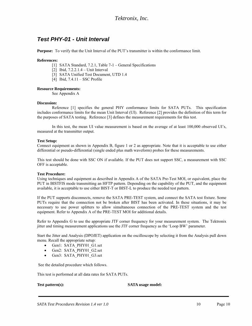
Setup oscilloscope with appropriate Vertical scale (full screen without clipping) and Horizontal scale. Horizontal resolution will vary depending on the SATA data rate and oscilloscope model. Select Math pull-down menu and establish Math1 = Ch1-Ch3. Run DPOJET by selecting ‘Jitter and Analysis’ in the oscilloscope’s pull down menu. Select Period/Freq tab and Period measurement on Math1 = Ch1-Ch3.
Click on the Right Arrow button in the Sources column. . In the Source Configuration Window, in the Source frame, verify that Math1 is the target source. Click on the “Setup…’ button in the Autoset frame of the same window. Set the Base Top Method to Min - Max
Select the Configure tab and define the following variables: Edges tab - Select Data
SATA Test Procedures Revision 1.4 ver 1.0 11 Page 11
Tektronix, Inc.
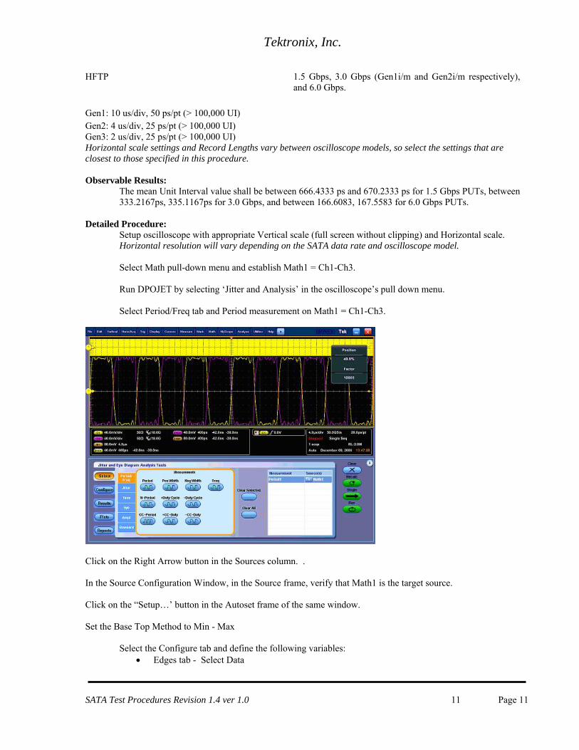
Filters tab – Select Low Pass Filter of 2nd Order, Freq (F2) = 1.98 MHz.
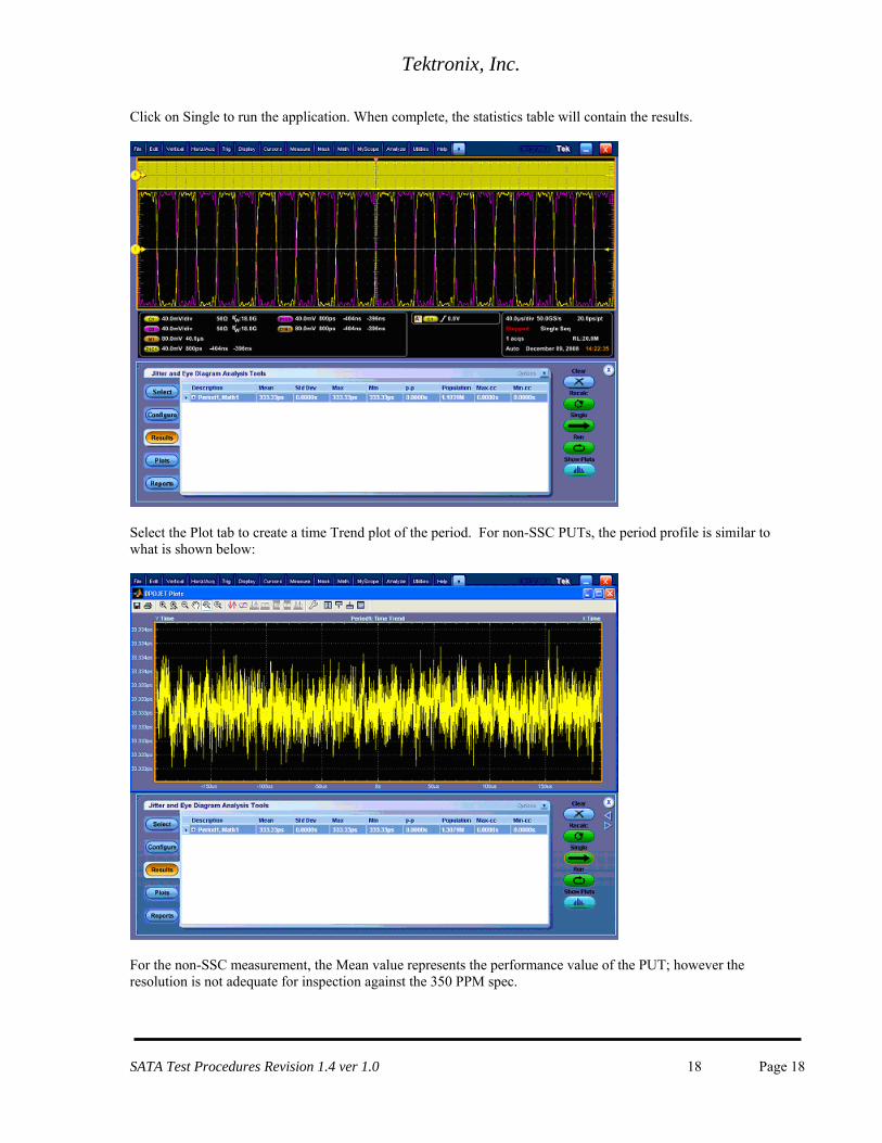
Click on Single to run the application. When complete, the statistics table will contain the results. An example of display is shown below.
Note that this measurement is rounded up from an internal representation of 9 digits. For measurements that are near the limit, it is possible to use the following procedure to view additional resolution on the measurement.
SATA Test Procedures Revision 1.4 ver 1.0 12 Page 12
Tektronix, Inc.
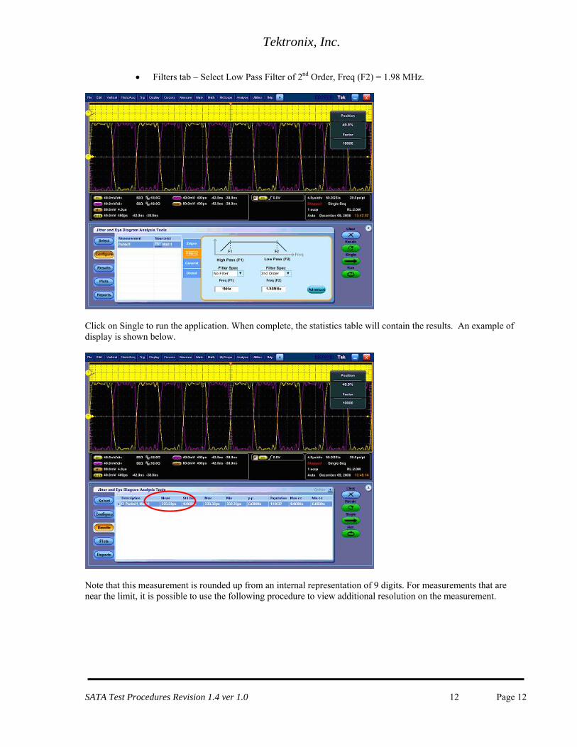
Select Plot tab to create a Time Trend plot of the period.
To get more measurement resolution, the data can be transferred to an oscilloscope Reference Waveform. Select the down arrow labeled ‘Options’ in the upper right corner of the Results window, and select “Export to Ref Waveform” from the pull-down menu. This will transfer the Period Profile data into the oscilloscope’s Ref Waveform memory.
SATA Test Procedures Revision 1.4 ver 1.0 13 Page 13
Tektronix, Inc.
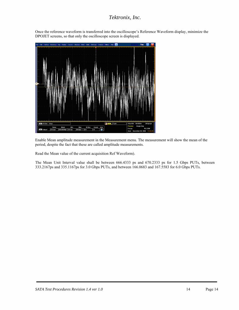
Once the reference waveform is transferred into the oscilloscope’s Reference Waveform display, minimize the DPOJET screens, so that only the oscilloscope screen is displayed.
Enable Mean amplitude measurement in the Measurement menu. The measurement will show the mean of the period, despite the fact that these are called amplitude measurements. Read the Mean value of the current acquisition Ref Waveform). The Mean Unit Interval value shall be between 666.4333 ps and 670.2333 ps for 1.5 Gbps PUTs, between 333.2167ps and 335.1167ps for 3.0 Gbps PUTs, and between 166.0683 and 167.5583 for 6.0 Gbps PUTs.
SATA Test Procedures Revision 1.4 ver 1.0 14 Page 14
Tektronix, Inc.
Test PHY-02 - Frequency Long Term Stability Purpose: To verify that the long term frequency stability of the PUT’s transmitter is within the conformance limit. References:
[1] SATA Standard, 7.2.1, Table 7-2 – General Specifications [2] Ibid, 7.2.2.1.4 – TX Frequency Long Term Stability [3] SATA Unified Test Document, UTD 1.4
Resource Requirements: See Appendix A. Discussion:
Reference [1] specifies the general PHY conformance limits for SATA PUTs. This specification includes conformance limits for the TX Frequency Long Term Stability. Reference [2] provides the definition of this term for the purposes of SATA testing. Reference [3] defines the measurement requirements for this test. Note: Per ECN-016, this test is now only performed on PUTs that DO NOT have SSC enabled. Test Setup: Connect equipment as shown in Appendix B, figure 1 or 2 as appropriate. Note that it is acceptable to use either differential or pseudo-differential (single ended plus math waveform) probes for these measurements. Test Procedure: Using techniques and equipment as described in Appendix A of the PRE-TEST MOI, or equivalent, place the PUT in BISTFIS mode transmitting an HFTP pattern. Depending on the capability of the PUT, and the equipment available, it is acceptable to use either BIST-T or BIST-L to produce the needed test pattern. If the PUT supports disconnects, remove the SATA PRE-TEST system, and connect SATA test fixture. Some PUTs require that the connection not be broken after BIST has been activated. In these situations, it may be necessary to use power splitters to allow simultaneous connection of the PRE-TEST system and the test equipment. Refer to Appendix A of the PRE-TEST MOI for additional details. Start the Jitter and Analysis (DPOJET) application on the oscilloscope by selecting it from the Analysis pull down menu. Open the oscilloscope’s File pull down menu to recall the setup SATA_PHY02_G3. See the detailed procedure which follows.
This test is performed once at the fastest data rate of the PUT.
Test pattern(s): HFTP
SATA usage model: 1.5 Gbps, 3.0 Gbps (Gen1i/m and Gen2i/m respectively), or 6.0 Gbps.
40 us/div (> 10 SSC periods), 25 ps/pt Horizontal scale settings and Record Lengths vary between oscilloscope models, so select the settings that are closest to those specified in this procedure Plot period vs. time. Record the maximum frequencies in the profile, using cursors.
SATA Test Procedures Revision 1.4 ver 1.0 15 Page 15
Tektronix, Inc.
Observable Results The Frequency Long Term Stability value shall be between +/- 350ppm for 1.5 Gbps, 3.0 Gbps, and 6Gbps PUTs.
Possible Problems: Section 7.4.11 of the SATA specification (version 2.5) requires the use of a low pass filter that is 60
times greater than the modulation frequency of the SSC. This equates to a 1.98MHz low pass filter for a 33kHz SSC. On some systems, the SSC profile may present a lot of noise as the cycle reaches its maximum frequency. For diagnostic purposes, it may be useful to reduce the filter from 1.98MHz to 1MHz (or even down to 300kHz in extreme cases). The new value should be selected to get a cleaner period time trend without changing the SSC modulation depth and frequency. Note that the altered setting is not valid for compliance tests.
Detailed Procedure:
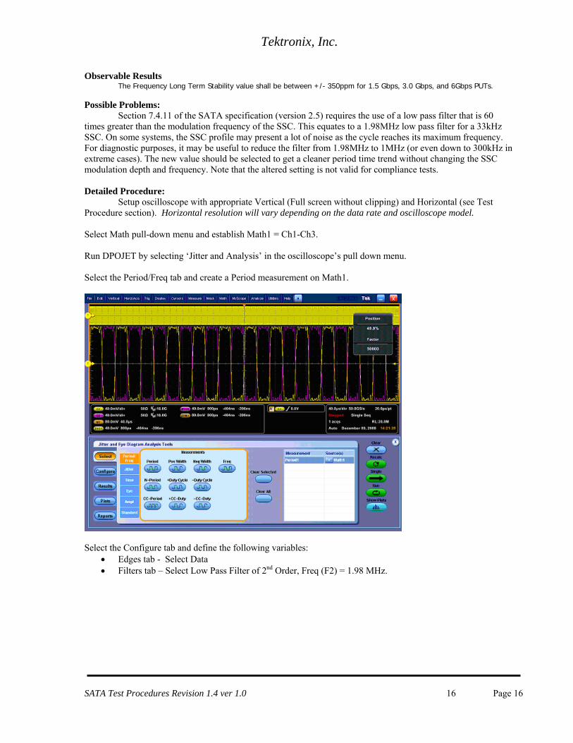
Setup oscilloscope with appropriate Vertical (Full screen without clipping) and Horizontal (see Test Procedure section). Horizontal resolution will vary depending on the data rate and oscilloscope model. Select Math pull-down menu and establish Math1 = Ch1-Ch3. Run DPOJET by selecting ‘Jitter and Analysis’ in the oscilloscope’s pull down menu. Select the Period/Freq tab and create a Period measurement on Math1.
Select the Configure tab and define the following variables:
Edges tab - Select Data Filters tab – Select Low Pass Filter of 2nd Order, Freq (F2) = 1.98 MHz.
SATA Test Procedures Revision 1.4 ver 1.0 16 Page 16
Tektronix, Inc.
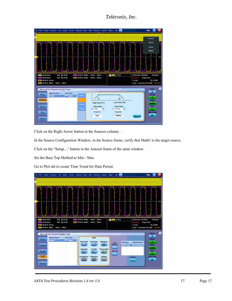
Click on the Right Arrow button in the Sources column. . In the Source Configuration Window, in the Source frame, verify that Math1 is the target source. Click on the “Setup…’ button in the Autoset frame of the same window. Set the Base Top Method to Min - Max Go to Plot tab to create Time Trend for Data Period.
SATA Test Procedures Revision 1.4 ver 1.0 17 Page 17
Tektronix, Inc.
Click on Single to run the application. When complete, the statistics table will contain the results.
Select the Plot tab to create a time Trend plot of the period. For non-SSC PUTs, the period profile is similar to what is shown below:
For the non-SSC measurement, the Mean value represents the performance value of the PUT; however the resolution is not adequate for inspection against the 350 PPM spec.
SATA Test Procedures Revision 1.4 ver 1.0 18 Page 18
Tektronix, Inc.
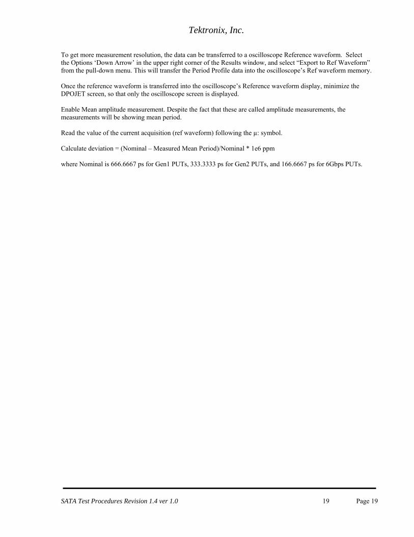
To get more measurement resolution, the data can be transferred to a oscilloscope Reference waveform. Select the Options ‘Down Arrow’ in the upper right corner of the Results window, and select “Export to Ref Waveform” from the pull-down menu. This will transfer the Period Profile data into the oscilloscope’s Ref waveform memory. Once the reference waveform is transferred into the oscilloscope’s Reference waveform display, minimize the DPOJET screen, so that only the oscilloscope screen is displayed. Enable Mean amplitude measurement. Despite the fact that these are called amplitude measurements, the measurements will be showing mean period. Read the value of the current acquisition (ref waveform) following the µ: symbol. Calculate deviation = (Nominal – Measured Mean Period)/Nominal * 1e6 ppm where Nominal is 666.6667 ps for Gen1 PUTs, 333.3333 ps for Gen2 PUTs, and 166.6667 ps for 6Gbps PUTs.
SATA Test Procedures Revision 1.4 ver 1.0 19 Page 19

Tektronix, Inc.
Test PHY-03 - Spread-Spectrum Modulation Frequency Purpose: To verify that the Spread Spectrum Modulation Frequency of the PUT’s transmitter is within the conformance limits. References:
[1] SATA Standard, 7.2.1, Table 27 – General Specifications [2] Ibid, 7.2.2.1.5 – Spread-Spectrum Modulation Frequency [3] SATA Unified Test Document, UTD 1.4 [4] Ibid, 7.4.11 – SSC Profile
Resource Requirements: See Appendix A. Last Template Modification: April 12, 2006 (Version 1.0) Discussion:
Reference [1] specifies the general PHY conformance limits for SATA PUTs. This specification includes conformance limits for the Spread-Spectrum Modulation Frequency. Reference [2] provides the definition of this term for the purposes of SATA testing. Reference [3] defines the measurement requirements for this test.
In this test, the Spread-Spectrum Modulation Frequency, fSSC, is measured, based on at least 10 complete
SSC cycles. Test Setup: Connect equipment as shown in Appendix B, figure 1 or 2 as appropriate. Note that it is acceptable to use either differential or pseudo-differential (single ended plus math waveform) probes for these measurements. Test Procedure: Using techniques and equipment as described in Appendix A of the PRE-TEST MOI, or equivalent, place the PUT in BISTFIS mode transmitting an HFTP pattern. Depending on the capability of the PUT, and the equipment available, it is acceptable to use either BIST-T or BIST-L to produce the needed test pattern. If the PUT supports disconnects, remove the SATA PRE-TEST system, and connect SATA test fixture. Some PUTs require that the connection not be broken after BIST has been activated. In these situations, it may be necessary to use power splitters to allow simultaneous connection of the PRE-TEST system and the test equipment. Refer to Appendix A of the PRE-TEST MOI for additional details. Start the Jitter and Analysis (DPOJET) application on the oscilloscope by selecting it from the Analysis pull down menu. In the oscilloscope File pull down menu, recall the setup SATA_PHY03_G3.set. See the detailed procedure which follows.
This test is performed once at the fastest data rate for the PUT. Test pattern(s): HFTP (SSC ON)
SATA usage model: 1.5 Gbps, 3.0 Gbps (Gen1i/m and Gen2i/m respectively), or 6.0 Gbps
40 us/div (> 10 SSC periods), 25 ps/pt Horizontal scale settings and Record Lengths vary between oscilloscope models, so select the settings that are closest to those specified in this procedure
SATA Test Procedures Revision 1.4 ver 1.0 20 Page 20

Tektronix, Inc.
Plot frequency vs. time. Cursor measurement: Record horizontal cursor positions of 10 SSC periods, divide by 10, invert period to SSC modulation frequency. Observable Results:
The Spread-Spectrum Modulation Frequency value shall be between 30 and 33 kHz for 1.5 Gbps, 3.0 Gbps, and 6.0 Gbps PUTs.
Detailed Procedure: Follow the procedure described for Phy-02, up to the point where the Time Trend Plot profile has been created. With SSC on, the resulting plot should be similar to the following.
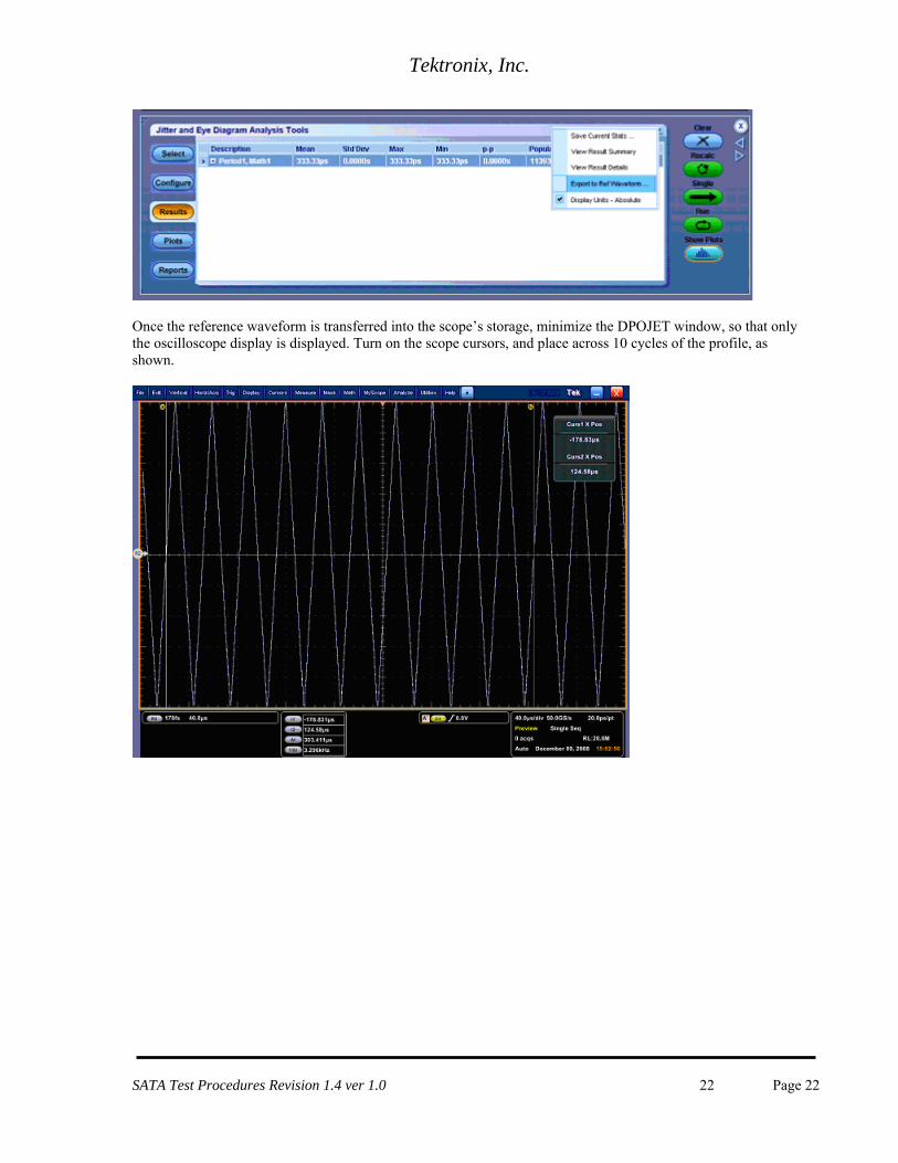
In some cases, it will be adequate to make the measurements using the cursor capability in DPOJET to measure the modulation frequency. Set cursors at the X axis crossing 10 cycles. To arrive at the modulation frequency, take the delta time value in the red bordered box in the upper right corner, divide by 10, and invert to get frequency. Note that there is often substantial higher frequency noise on this profile, and it may be difficult to discern the X axis measurement points on the profile. This is especially critical if the PUT is close to either limit. In this case, it may be preferable to move the waveform into the scope’s reference waveform storage, and perform a more critical inspection there. This can be accomplished by using the following process: Select the Options ‘Down Arrow’ in the upper right corner of the Results window, and select “Export to Ref Waveform” from the pull-down menu. This will transfer the Period Profile data into the oscilloscope’s Ref waveform memory.
SATA Test Procedures Revision 1.4 ver 1.0 21 Page 21
Tektronix, Inc.
Once the reference waveform is transferred into the scope’s storage, minimize the DPOJET window, so that only the oscilloscope display is displayed. Turn on the scope cursors, and place across 10 cycles of the profile, as shown.
SATA Test Procedures Revision 1.4 ver 1.0 22 Page 22
Tektronix, Inc.
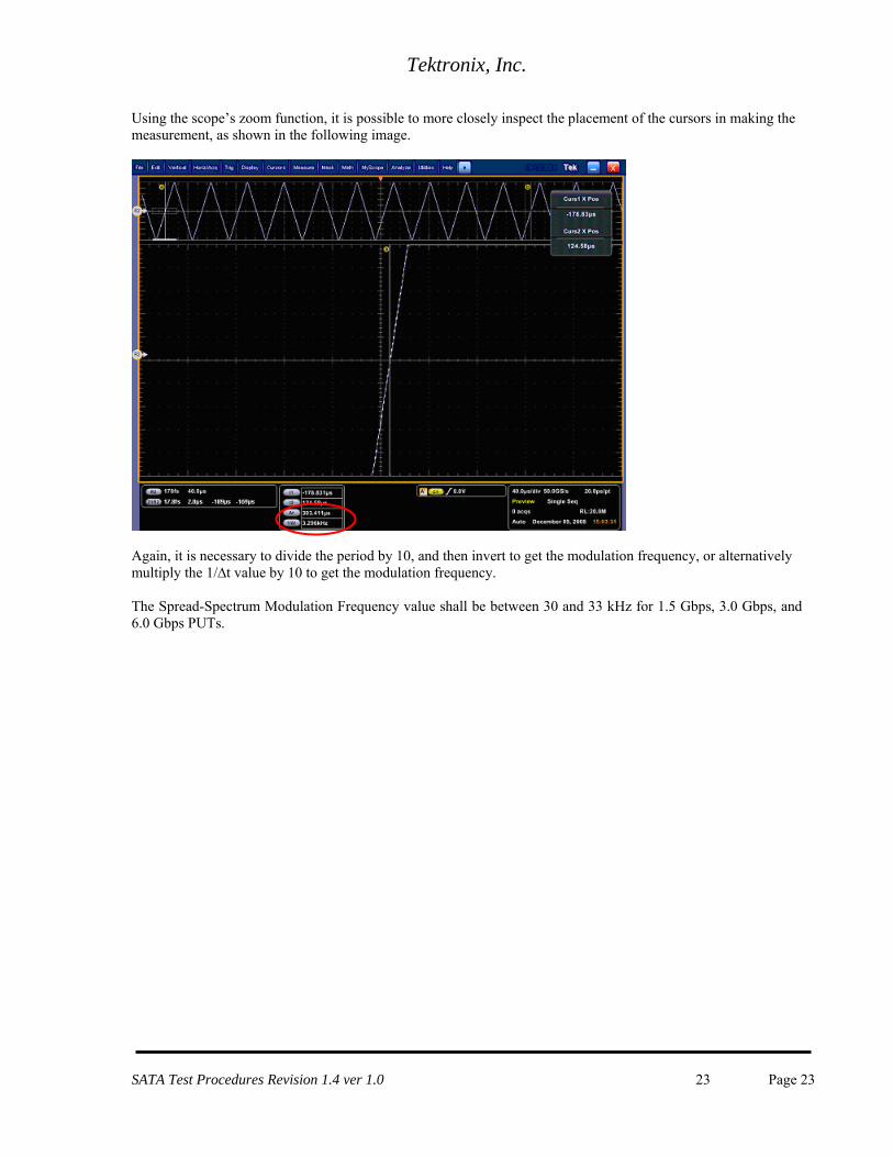
Using the scope’s zoom function, it is possible to more closely inspect the placement of the cursors in making the measurement, as shown in the following image.
Again, it is necessary to divide the period by 10, and then invert to get the modulation frequency, or alternatively multiply the 1/∆t value by 10 to get the modulation frequency. The Spread-Spectrum Modulation Frequency value shall be between 30 and 33 kHz for 1.5 Gbps, 3.0 Gbps, and 6.0 Gbps PUTs.
SATA Test Procedures Revision 1.4 ver 1.0 23 Page 23
Tektronix, Inc.
Test PHY-04 - Spread-Spectrum Modulation Deviation Purpose: To verify that the Spread-Spectrum Modulation Deviation of the PUT’s transmitter is within the conformance limits. References:
[1] SATA Standard, 7.2.1, Table 27 – General Specifications [2] Ibid, 7.2.2.1.6 – Spread-Spectrum Modulation Deviation [3] SATA Unified Test Document, UTD 1.4
Resource Requirements: See Appendix A. Discussion:
Reference [1] specifies the general PHY conformance limits for SATA PUTs. This specification includes conformance limits for the Spread-Spectrum Modulation Deviation. Reference [2] provides the definition of this term for the purposes of SATA testing. Reference [3] defines the measurement requirements for this test.
The measured Spread-Spectrum Modulation Deviation is based on at least 10 complete SSC cycles. Test Setup:
Connect equipment as shown in Appendix B, figure 1 or 2 as appropriate. Note that it is acceptable to use either differential or pseudo-differential (single ended plus math waveform) probes for these measurements. Test Procedure:
Using techniques and equipment as described in Appendix A of the PRE-TEST MOI, or equivalent, place the PUT in BISTFIS mode transmitting an HFTP pattern. Depending on the capability of the PUT, and the equipment available, it is acceptable to use either BIST-T or BIST-L to produce the needed test pattern. If the PUT supports disconnects, remove the SATA PRE-TEST system, and connect SATA test fixture. Some PUTs require that the connection not be broken after BIST has been activated. In these situations, it may be necessary to use power splitters to allow simultaneous connection of the PRE-TEST system and the test equipment. Refer to Appendix A of the PRE-TEST MOI for additional details. Start the Jitter and Analysis (DPOJET) application on the oscilloscope by selecting it from the Analysis pull down menu. In the oscilloscope’s File pull down menu, recall the setup SATA_PHY04_G3. See the detailed procedure which follows.
This test is performed once at the fastest data rate for the PUT. Test pattern(s): HFTP (SSC ON)
SATA usage model: 1.5 Gbps, 3.0 Gbps (Gen1i/m and Gen2i/m respectively), or 6.0 Gbps
40 us/div (> 10 SSC periods), 25 ps/pt Horizontal scale settings and Record Lengths vary between oscilloscope models, so select the settings that are closest to those specified in this procedure Record min, max frequency from results overview. Calculate deviation=( Nominal – Measured Mean Max Period)/Nominal * 1e6 ppm. No greater than -5350 (+350 to -5350) assuming (Nominal – Measured Mean Max Period)/Nominal * 1e6 ppm
SATA Test Procedures Revision 1.4 ver 1.0 24 Page 24

Tektronix, Inc.
Observable Results:
The Spread-Spectrum Modulation Deviation value shall be between –5350 and +350 ppm for 1.5 Gbps, 3.0 Gbps, and 6.0 Gbps PUTs.
Detailed Procedure: Follow the procedure described for PHY-02, up to the point where the Time Trend Plot profile has been created. With SSC on, the resulting plot should be similar to the following.
NOTE: DPOJET provides the ability to do cursor measurements directly on the Time Trend profile plot. However, the 4 digits of resolution obtained when using DPOJET cursor measurements (1000 ppm) is not sufficient for this test. The value can also be read directly from the Results table as seen in the next figure. This data is shown as 5 digits, and provides a 100 ppm resolution, which is marginally adequate for the measurement tolerance.
SATA Test Procedures Revision 1.4 ver 1.0 25 Page 25
Tektronix, Inc.
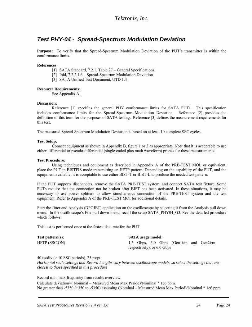
To get 8 digits of resolution, select the Options ‘Down Arrow’ in the upper right corner of the Results window, and select “Export to Ref Waveform” from the pull-down menu. This will transfer the Period Profile data into the oscilloscope’s Ref waveform memory.
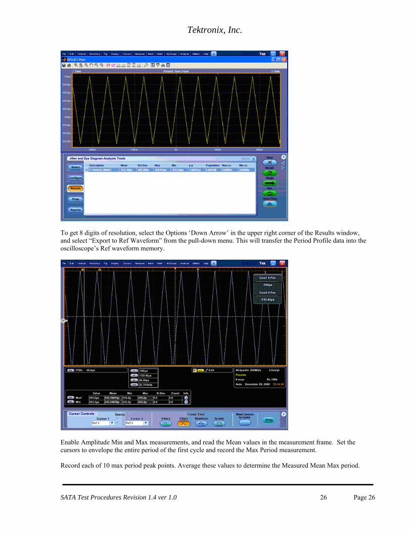
Enable Amplitude Min and Max measurements, and read the Mean values in the measurement frame. Set the cursors to envelope the entire period of the first cycle and record the Max Period measurement. Record each of 10 max period peak points. Average these values to determine the Measured Mean Max period.
SATA Test Procedures Revision 1.4 ver 1.0 26 Page 26
Tektronix, Inc.
Record each of 10 min period peak points. Average these values to determine the Measured Mean Min period. Calculate deviation = (Nominal – Measured Mean Max)/Nominal * 1e6 ppm Calculate deviation = (Nominal – Measured Mean Min Period)/Nominal * 1e6 ppm, where Nominal is 666.6667 ps for 1.5 Gbps PUTs, 333.3333 ps for 3.0 Gbps PUTs, and 166.6667 ps for 6.0 Gbps PUTs.
SATA Test Procedures Revision 1.4 ver 1.0 27 Page 27
Tektronix, Inc.
PHY TRANSMITTED SIGNAL REQUIREMENTS (TSG 1-16) Overview:
This group of tests verifies the Phy Transmitted Signal Requirements, as defined in Section 2.14 of the SATA Interoperability Unified Test Document, UTD 1.4 (which references the SATA Standard, v3.0).
SATA Test Procedures Revision 1.4 ver 1.0 28 Page 28
Tektronix, Inc.
Test TSG-01 - Differential Output Voltage Purpose: To verify that the Differential Output Voltage of the PUT’s transmitter is within the conformance limits. References:
[1] SATA Standard, 7.2.1, Table 29 – Transmitted Signal Requirements [2] Ibid, 7.4.2.1 – TX Differential Output Voltage [3] SATA Unified Test Document UTD 1.4
Resource Requirements: See Appendix A Discussion:
Reference [1] specifies the Transmitted Signal conformance limits for SATA PUTs. This specification includes conformance limits for the Differential Output Voltage. Reference [2] provides the definition of this term for the purposes of SATA testing. Reference [3] defines the measurement requirements for this test.
Test Setup:
Connect equipment as shown in Appendix B, figure 1 or 2 as appropriate. Note that it is acceptable to use either differential or pseudo-differential (single ended plus math waveform) probes for these measurements. Test Procedure:
Using techniques and equipment as described in Appendix A of the PRE-TEST MOI, or equivalent, place the PUT in BISTFIS mode transmitting an HFTP pattern. Depending on the capability of the PUT, and the equipment available, it is acceptable to use either BIST-T or BIST-L to produce the needed test pattern. If the PUT supports disconnects, remove the SATA PRE-TEST system, and connect SATA test fixture. Some PUTs require that the connection not be broken after BIST has been activated. In these situations, it may be necessary to use power splitters to allow simultaneous connection of the PRE-TEST system and the test equipment. Refer to Appendix A of the PRE-TEST MOI for additional details. For products which support 3.0 and 6.0 Gbps, this requirement must be tested at the interface rates of 1.5 Gbps and 3Gbps). For SATA Gen3 PUTs (6Gbps), refer to the procedure in TSG-15 of this document. Test pattern(s): HFTP, MFTP, and LFTP, and LBP or HFTP, MFTP, and LFTP (SSC optional)
SATA usage model: 1.5 Gbps and 3.0 Gbps (Gen1i/m and Gen2i/m respectively)
Gen1: 10 us/div, 50 ps/pt (> 100,000 UI) Gen2: 4 us/div, 25 ps/pt (> 100,000 UI) Observable Results: For the interests of the Interoperability Program, the measurements will only be taken to verify this requirement at the minimum limit of 400mVppd. Within the specification, there are two options for measuring the minimum:
- Vtest = min(DH, DM, VtestLBP) - Vtest = min(DH, DM, VtestAPP)
SATA Test Procedures Revision 1.4 ver 1.0 29 Page 29
Tektronix, Inc.
Note that gathering a minimum result from either of the options above is acceptable. It is not required to report a result for both. The pu/pl measurements outlined in the specification are to be taken, but the results are informative
Note that the pu/pl measurements outlined in the specification are to be taken, but the results are informative. There is not verification of maximum limit values for this measurement. In the interest of ensuring products meet some metric for system interoperability at the maximum limit, the maximum value received out of the minimum measurement will be verified to not exceed 800mV using the formulas below, where DH, DM, VtestLBP, and VtestAPP are the same values used for the above minimum measurement.
- Vtest(max) = max(DH, DM, VtestLBP) - Vtest(max) = max(DH, DM, VtestAPP)
Possible Problems: Per ECN-18, a new LBP pattern was defined that eliminates the disparity ambiguity, as described below. Use ECN-18 compliant LBP for performing the amplitude test whenever possible. If an ECN-18 LBP is not available, it is possible to use the older LBP pattern. However, a pattern mismatch error can occur. To avoid the pattern mismatch problem, make sure that the real lone bit pattern with positive disparity is used (0011 0110 1111 0100 0010 0011 0110 1111 0100 0010 0011 0110 etc….). This pattern has a lone ‘1’ bit between 4 ‘0’s and 3 ‘0’s, and is required for the algorithm. Visually verify the proper disparity on LBP by zooming in on the acquired waveform, and inspecting the waveform for a section that contains a “00001000” section. If this pattern is not readily apparent, re-load the LBP BISTFIS pattern into the PUT, and reacquire the waveform, then repeat the inspection until the proper pattern is seen. Once the proper pattern is detected, continue running the test. It is only necessary to make this inspection on LBP patterns, as there is a 50% chance of getting the desired positive disparity each time the LBP is loaded into the PUT. Part I Detailed Procedure:
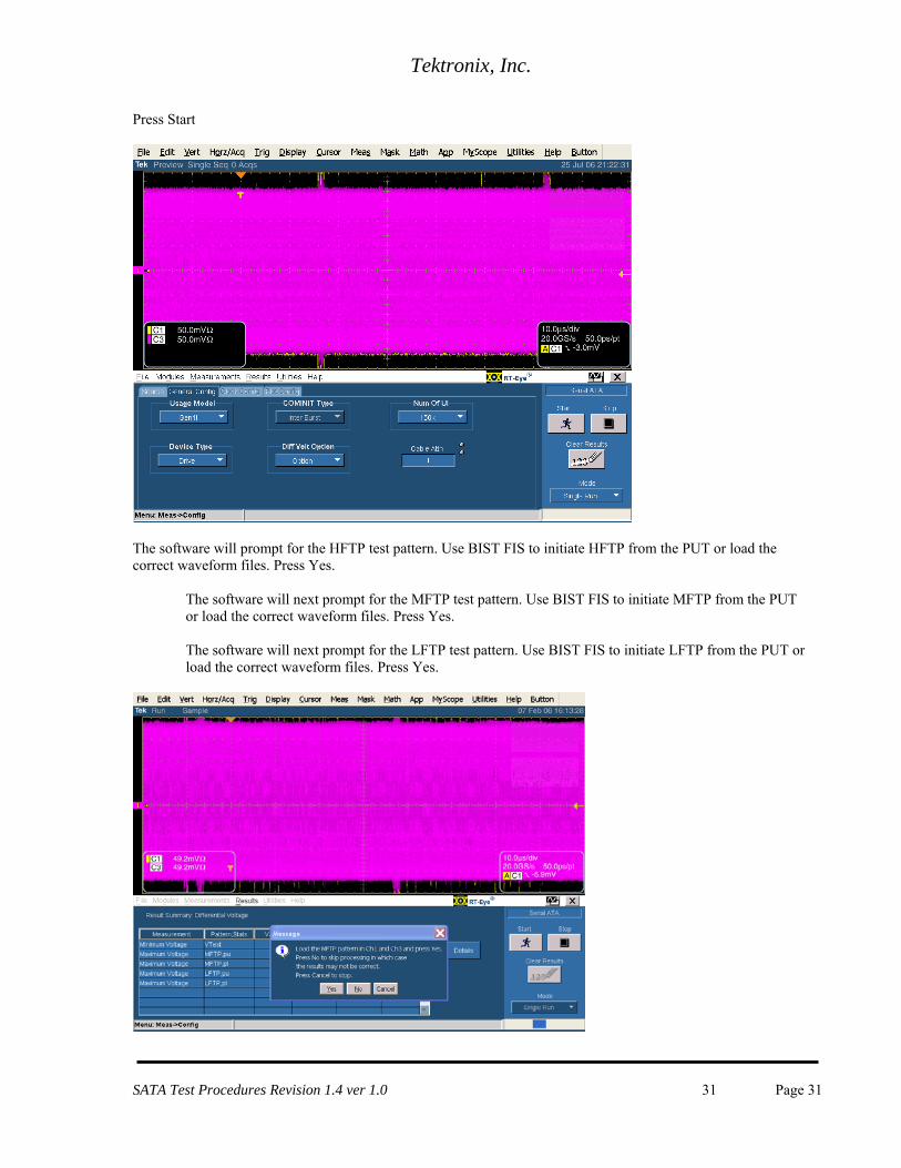
Start RT-Eye application on Scope. Select SATA module under “Modules” menu item. Select Differential Voltage from Amplitude Measurement. Select correct probe type. Press configure. Source configuration (Source tab): Select BIST FIS/User Test Method. Select correct Source Type and channels.
General configuration (General Config tab): Select correct Usage Model, Device Type, Diff Volt Option Option2, and Number of UI 150k.
SATA Test Procedures Revision 1.4 ver 1.0 30 Page 30
Tektronix, Inc.
Press Start
The software will prompt for the HFTP test pattern. Use BIST FIS to initiate HFTP from the PUT or load the correct waveform files. Press Yes.
The software will next prompt for the MFTP test pattern. Use BIST FIS to initiate MFTP from the PUT or load the correct waveform files. Press Yes. The software will next prompt for the LFTP test pattern. Use BIST FIS to initiate LFTP from the PUT or load the correct waveform files. Press Yes.
SATA Test Procedures Revision 1.4 ver 1.0 31 Page 31
Tektronix, Inc.
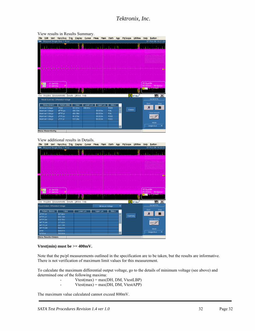
View results in Results Summary.
View additional results in Details.
Vtest(min) must be >= 400mV. Note that the pu/pl measurements outlined in the specification are to be taken, but the results are informative. There is not verification of maximum limit values for this measurement. To calculate the maximum differential output voltage, go to the details of minimum voltage (see above) and determined one of the following maxima:
- Vtest(max) = max(DH, DM, VtestLBP) - Vtest(max) = max(DH, DM, VtestAPP)
The maximum value calculated cannot exceed 800mV.
SATA Test Procedures Revision 1.4 ver 1.0 32 Page 32
Tektronix, Inc.
Test TSG-02 - Rise/Fall Time Purpose: To verify that the Rise/Fall time of the PUT’s transmitter is within the conformance limits. References:
[1] SATA Standard, 7.2.1, Table 29 – Transmitted Signal Requirements [2] Ibid, 7.2.2.3.3 – TX Rise/Fall Time [3] SATA Unified Test Document, 2.12.2
Resource Requirements: See Appendix A. Discussion:
Reference [1] specifies the Transmitted Signal conformance limits for SATA PUTs. This specification includes conformance limits for the Rise/Fall Time. Reference [2] provides the definition of this term for the purposes of SATA testing. Reference [3] defines the measurement requirements for this test. Test Setup:
Connect equipment as shown in Appendix B, figure 1 or 2 as appropriate. Note that it is acceptable to use either differential or pseudo-differential (single ended plus math waveform) probes for these measurements. Test Procedure:
Using techniques and equipment as described in Appendix A of the PRE-TEST MOI, or equivalent, place the PUT in BISTFIS mode transmitting an HFTP pattern. Depending on the capability of the PUT, and the equipment available, it is acceptable to use either BIST-T or BIST-L to produce the needed test pattern. If the PUT supports disconnects, remove the SATA PRE-TEST system, and connect SATA test fixture. Some PUTs require that the connection not be broken after BIST has been activated. In these situations, it may be necessary to use power splitters to allow simultaneous connection of the PRE-TEST system and the test equipment. Refer to Appendix A of the PRE-TEST MOI for additional details. Start the Jitter and Analysis (DPOJET) application on the oscilloscope by selecting it from the Analysis pull down menu. In the File pull down menu recall the appropriate setup:
Gen1: SATA_TSG02_G1 Gen2: SATA_TSG02_G2 Gen3: SATA_TSG02_G3
Horizontal settings will need to be adjusted according to the SATA data rate being tested. See the following detailed procedure for additional information. This requirement must be tested at all interface rates. The LFTP pattern defined in section 4.1.75 of the SATA Revision 3.0 specification is used for all rise time and fall time measurements to ensure consistency. Test pattern(s): LFTP (SSC optional)
SATA usage model: 1.5 Gbps, 3.0 Gbps (Gen1i/m and Gen2i/m respectively), and 6.0 Gbps (Gen3i)
Gen1: 10 us/div, 50 ps/pt (> 100,000 UI) Gen2: 4 us/div, 25 ps/pt (> 100,000 UI) Gen3: 2 us/div, 25 ps/pt (> 100,000 UI) Horizontal scale settings and Record Lengths vary between oscilloscope models, so select the settings that are closest to those specified in this procedure. Observable Results:
SATA Test Procedures Revision 1.4 ver 1.0 33 Page 33

Tektronix, Inc.
The TX Rise/Fall Times shall be between the limits specified in reference [1]. For convenience, the values are reproduced below. Note: Failures at minimum rate have not been shown to affect interoperability and will not be included in determining pass/fail for Interop testing
PUT Type RFT Min RFT Max Gen1i and Gen1m 100 ps 273 ps Gen2i and Gen2m 67 ps 136 ps
Gen3 33 68 Detailed Procedure:
Setup the oscilloscope with appropriate Vertical (Full screen without clipping) and Horizontal (see Test Procedure section). Horizontal resolution will vary depending on the data rate and oscilloscope model.
In the ‘Math’ pull down menu, define Math1 as Ch1-Ch3 Start the Jitter and Eye Analysis (DPOJET) program from the Analysis pull down menu on the oscilloscope, and choose ‘Select’. Select the Time tab, and add measurements for Rise Time and Fall Time.
Click on the Rise Time1 measurement row. Click on the Right Arrow button in the Sources column. . In the Source Configuration Window, in the Source frame, designate Math1 as the target source. Click on the “Setup…’ button in the Autoset frame of the same window. Set the Rise High and Fall High to 80%. Set the Rise Low and Fall Low to 20%. Set the Base Top Method to Min - Max
SATA Test Procedures Revision 1.4 ver 1.0 34 Page 34
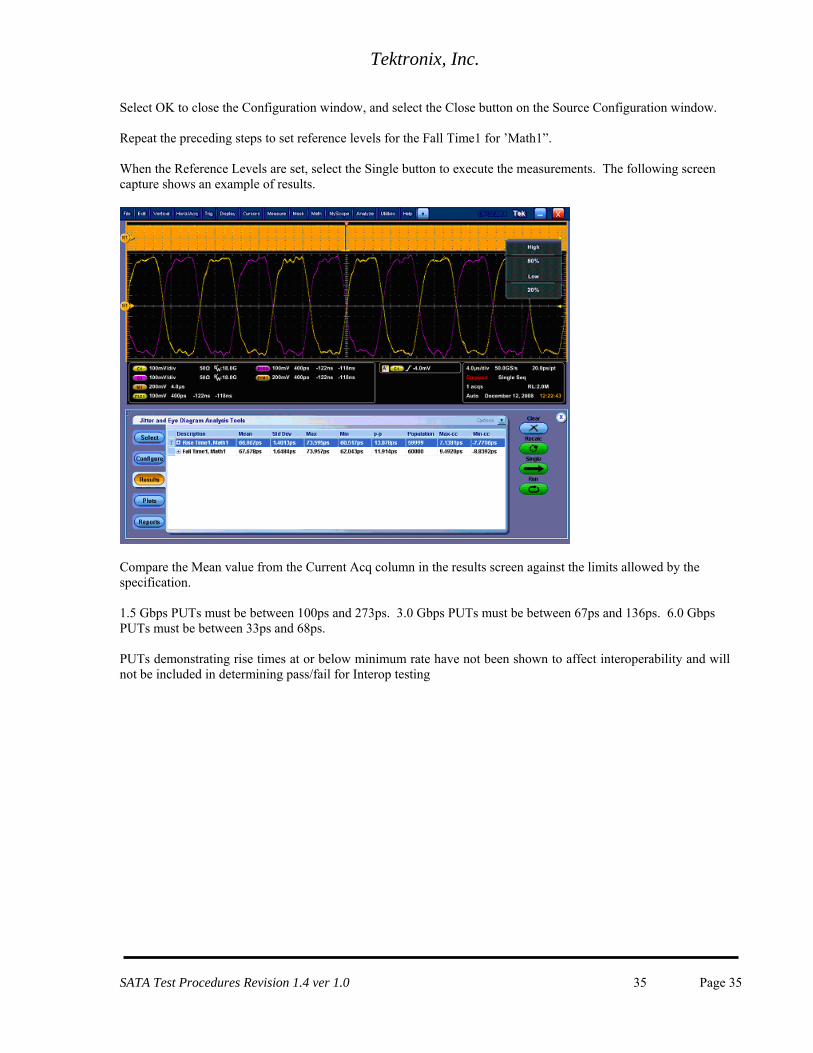
Tektronix, Inc.
Select OK to close the Configuration window, and select the Close button on the Source Configuration window. Repeat the preceding steps to set reference levels for the Fall Time1 for ’Math1”. When the Reference Levels are set, select the Single button to execute the measurements. The following screen capture shows an example of results.
Compare the Mean value from the Current Acq column in the results screen against the limits allowed by the specification. 1.5 Gbps PUTs must be between 100ps and 273ps. 3.0 Gbps PUTs must be between 67ps and 136ps. 6.0 Gbps PUTs must be between 33ps and 68ps. PUTs demonstrating rise times at or below minimum rate have not been shown to affect interoperability and will not be included in determining pass/fail for Interop testing
SATA Test Procedures Revision 1.4 ver 1.0 35 Page 35
Tektronix, Inc.
Test TSG-03 - Differential Skew Purpose: To verify that the Differential Skew of the PUT’s transmitter is within the conformance limits. References:
[1] SATA Standard, 7.2.1, Table 29 – Transmitted Signal Requirements [2] Ibid, 7.2.2.3.4 – TX Differential Skew (Gen2i, Gen1x, Gen2x) [3] Ibid, 7.4.12 – Intra-pair Skew [4] SATA Unified Test Document, UTD 1.4
Resource Requirements: See Appendix A. Last Template Modification: April 12, 2006 (Version 1.0) Discussion:
Reference [1] specifies the Transmitted Signal conformance limits for SATA PUTs. This specification includes conformance limits for Differential Skew. Reference [2] provides the definition of this term for the purposes of SATA testing. Reference [3] defines the measurement requirements for this test.
Test Setup:
Connect equipment as shown in Appendix B, figure 1A or 2A as appropriate. Note that it is only acceptable to use two single ended SMA connections for these measurements. Test Procedure:
Using techniques and equipment as described in Appendix A of the PRE-TEST MOI, or equivalent, place the PUT in BISTFIS mode transmitting an HFTP pattern. Depending on the capability of the PUT, and the equipment available, it is acceptable to use either BIST-T or BIST-L to produce the needed test pattern. If the PUT supports disconnects, remove the SATA PRE-TEST system, and connect SATA test fixture. Some PUTs require that the connection not be broken after BIST has been activated. In these situations, it may be necessary to use power splitters to allow simultaneous connection of the PRE-TEST system and the test equipment. Refer to Appendix A of the PRE-TEST MOI for additional details. Start the Jitter and Analysis (DPOJET) application on the oscilloscope by selecting it from the Analysis pull down menu. In the File pull down menu recall the appropriate setup:
Gen1: SATA_TSG03_G1 Gen2: SATA_TSG03_G2 Gen3: SATA_TSG03_G3
Horizontal settings will need to be adjusted according to the SATA data rate being tested. Take the average of both skew results. See the following detailed procedure for additional information. Repeat the PRE-TEST procedure described above for each specified test pattern. This test is only done at the fastest data rate of the PUT. Testing with SSC is optional. Test pattern(s): HFTP, MFTP (SSC optional)
SATA usage model: 1.5 Gbps, 3.0 Gbps (Gen1i/m and Gen2i/m respectively), or 6.0 Gbps
Gen1: 10 us/div, 50 ps/pt (> 100,000 UI) Gen2: 4 us/div, 25 ps/pt (> 100,000 UI) Gen3: 2 us/div, 25 ps/pt (> 100,000 UI)
SATA Test Procedures Revision 1.4 ver 1.0 36 Page 36
Tektronix, Inc.
Horizontal scale settings and Record Lengths vary between oscilloscope models, so select the settings that are closest to those specified in this procedure. Observable Results:
The TX Differential Skew shall be no greater than the Max value specified in reference [1]. For convenience, the values are reproduced below.
PUT Type Max Diff Skew Gen1i and Gen1m 20 ps Gen2i and Gen2m 20 ps
Gen3 20 ps Detailed Procedure:
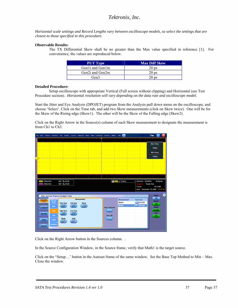
Setup oscilloscope with appropriate Vertical (Full screen without clipping) and Horizontal (see Test Procedure section). Horizontal resolution will vary depending on the data rate and oscilloscope model.
Start the Jitter and Eye Analysis (DPOJET) program from the Analysis pull down menu on the oscilloscope, and choose ‘Select’. Click on the Time tab, and add two Skew measurements (click on Skew twice). One will be for the Skew of the Rising edge (Skew1). The other will be the Skew of the Falling edge (Skew2). Click on the Right Arrow in the Source(s) column of each Skew measurement to designate the measurement is from Ch1 to Ch3.
Click on the Right Arrow button in the Sources column. . In the Source Configuration Window, in the Source frame, verify that Math1 is the target source. Click on the “Setup…’ button in the Autoset frame of the same window. Set the Base Top Method to Min – Max. Close the window.
SATA Test Procedures Revision 1.4 ver 1.0 37 Page 37
Tektronix, Inc.
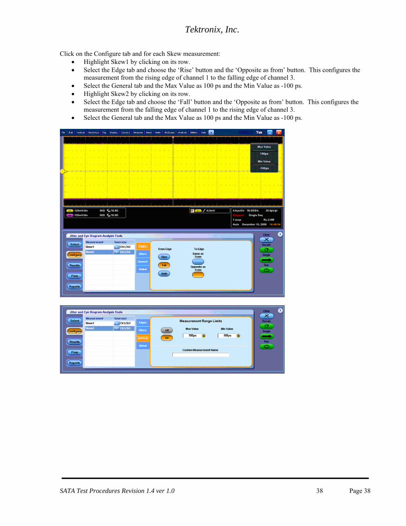
Click on the Configure tab and for each Skew measurement: Highlight Skew1 by clicking on its row. Select the Edge tab and choose the ‘Rise’ button and the ‘Opposite as from’ button. This configures the
measurement from the rising edge of channel 1 to the falling edge of channel 3. Select the General tab and the Max Value as 100 ps and the Min Value as -100 ps. Highlight Skew2 by clicking on its row. Select the Edge tab and choose the ‘Fall’ button and the ‘Opposite as from’ button. This configures the
measurement from the falling edge of channel 1 to the rising edge of channel 3. Select the General tab and the Max Value as 100 ps and the Min Value as -100 ps.
SATA Test Procedures Revision 1.4 ver 1.0 38 Page 38
Tektronix, Inc.
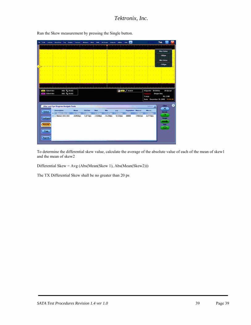
Run the Skew measurement by pressing the Single button.
To determine the differential skew value, calculate the average of the absolute value of each of the mean of skew1 and the mean of skew2 Differential Skew = Avg (Abs(Mean(Skew 1), Abs(Mean(Skew2))) The TX Differential Skew shall be no greater than 20 ps
SATA Test Procedures Revision 1.4 ver 1.0 39 Page 39
Tektronix, Inc.
Test TSG-04 - AC Common Mode Voltage Purpose: To verify that the AC Common Mode Voltage of the PUT’s transmitter is within the conformance limits. References:
[1] SATA Standard, 7.2.1, Table 29 – Transmitted Signal Requirements [2] Ibid, 7.2.2.3.5 – TX AC Common Mode Voltage [3] SATA Unified Test Document, UTD 1.4
Resource Requirements: See Appendix A. Discussion:
Reference [1] specifies the Transmitted Signal conformance limits for SATA PUTs. This specification includes conformance limits for the TX AC Common Mode Voltage. Reference [2] provides the definition of this term for the purposes of SATA testing. Reference [3] defines the measurement requirements for this test. Test Setup:
Connect equipment as shown in Appendix B, figure 1A or 2A as appropriate. Note that it is only acceptable to use two single ended SMA connections for these measurements. Test Procedure:
Using techniques and equipment as described in Appendix A of the PRE-TEST MOI, or equivalent, place the PUT in BISTFIS mode transmitting an MFTP pattern. Depending on the capability of the PUT, and the equipment available, it is acceptable to use either BIST-T or BIST-L to produce the needed test pattern. If the PUT supports disconnects, remove the SATA PRE-TEST system, and connect SATA test fixture. Some PUTs require that the connection not be broken after BIST has been activated. In these situations, it may be necessary to use power splitters to allow simultaneous connection of the PRE-TEST system and the test equipment. Refer to Appendix A of the PRE-TEST MOI for additional details. For SATA Gen2 PUTs (3.0 Gbps), start the RT-Eye application on Scope. Select SATA module under “Modules” menu item. Select AC CM Voltage from the Amplitude measurements menu. Refer to the detailed procedure below. This is only done for Gen2 PUTs. Testing with SSC as optional. For SATA Gen3 PUTs (6.0 Gbps), Refer to the detailed procedure in TSG-16 of this document. Test pattern(s): MFTP SSC optional)
SATA usage model: 3.0 Gbps
Gen2: 4 us/div, 25 ps/pt (> 100,000 UI) Horizontal scale settings and Record Lengths vary between oscilloscope models, so select the settings that are closest to those specified in this procedure. Observable Results:
The AC Common Mode Voltage value shall be less than or equal to 50 mVp-p for Gen2i and Gen2m PUTs. Detailed Procedure:
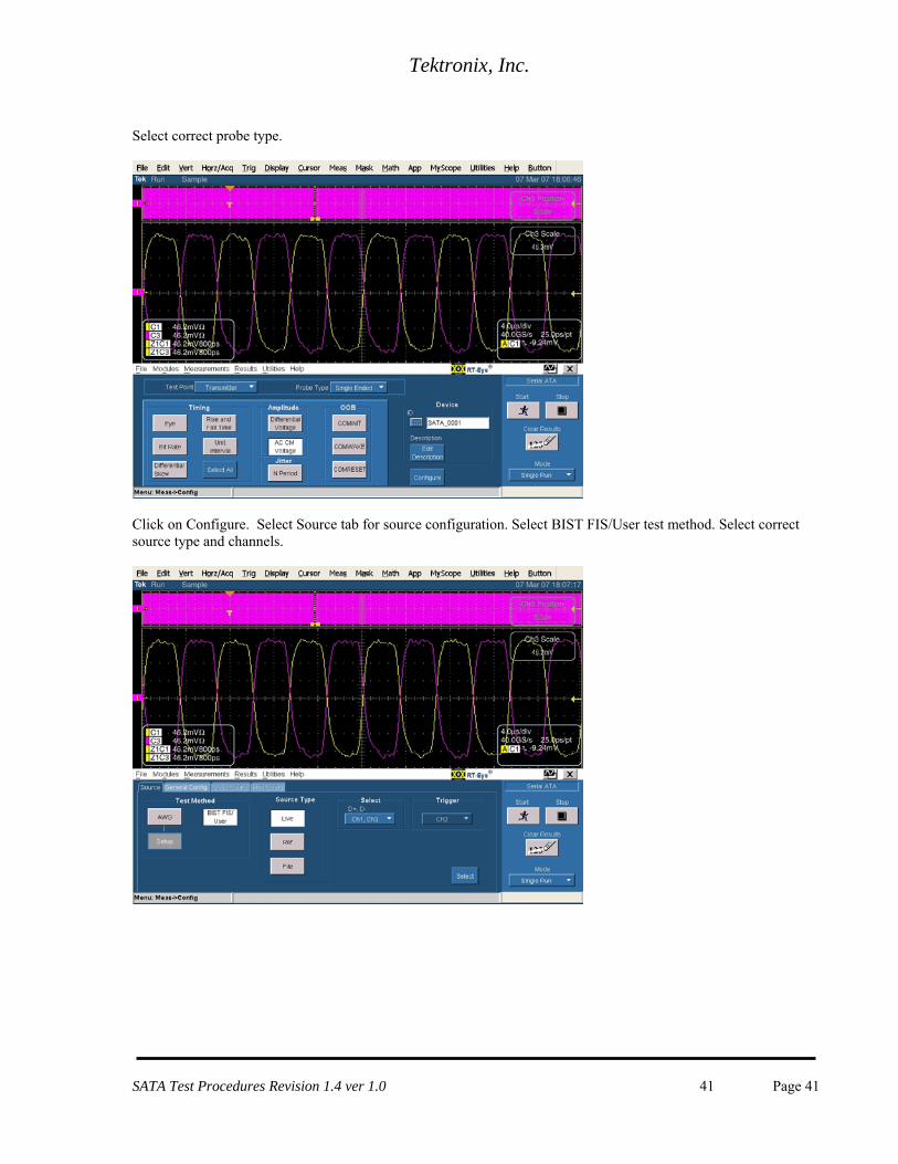
Start RT-Eye application on Scope. Select SATA module under “Modules” menu item. Select “AC CM Voltage” in Amplitude frame.
SATA Test Procedures Revision 1.4 ver 1.0 40 Page 40
Tektronix, Inc.
Select correct probe type.
Click on Configure. Select Source tab for source configuration. Select BIST FIS/User test method. Select correct source type and channels.
SATA Test Procedures Revision 1.4 ver 1.0 41 Page 41
Tektronix, Inc.
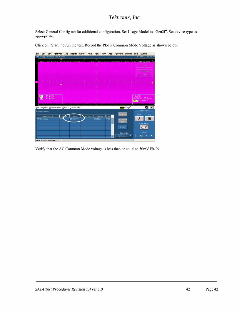
Select General Config tab for additional configuration. Set Usage Model to “Gen2i”. Set device type as appropriate. Click on “Start” to run the test. Record the Pk-Pk Common Mode Voltage as shown below.
Verify that the AC Common Mode voltage is less than or equal to 50mV Pk-Pk.
SATA Test Procedures Revision 1.4 ver 1.0 42 Page 42
Tektronix, Inc.
Test TSG-05 - Rise/Fall Imbalance (Obsolete) Purpose: To verify that the Rise/Fall Imbalance of the PUT’s transmitter is within the conformance limits. References:
[1] SATA Standard, 7.2.1, Table 29 – Transmitted Signal Requirements [2] Ibid, 7.2.2.3.9 – TX Rise/Fall Imbalance [3] SATA Unified Test Document, UTD 1.4
Resource Requirements: See Appendix A. Discussion:
Reference [1] specifies the Transmitted Signal conformance limits for SATA PUTs. This specification includes conformance limits for the Rise/Fall Imbalance. Reference [2] provides the definition of this term for the purposes of SATA testing. Reference [3] defines the measurement requirements for this test. Test Setup: Connect equipment as shown in Appendix B, figure 1A or 2A as appropriate. Single ended measurements using SMA cables are recommended. Test Procedure: Using techniques and equipment as described in Appendix A of the PRE-TEST MOI, or equivalent, place the PUT in BISTFIS mode transmitting an HFTP pattern. Depending on the capability of the PUT, and the equipment available, it is acceptable to use either BIST-T or BIST-L to produce the needed test pattern. If the PUT supports disconnects, remove the SATA PRE-TEST system, and connect SATA test fixture. Some PUTs require that the connection not be broken after BIST has been activated. In these situations, it may be necessary to use power splitters to allow simultaneous connection of the PRE-TEST system and the test equipment. Refer to Appendix A of the PRE-TEST MOI for additional details. Start the Jitter and Analysis (DPOJET) application on the oscilloscope by selecting it from the Analysis pull down menu. In the Oscilloscope File pull down menu recall SATA_TSG05_G2.set. See the following detailed procedure for additional information. This is only done for Gen2 devices. Testing with SSC is optional. Repeat the PRE-TEST procedure and measurement for MFTP. Test pattern(s): HFTP, MFTP (SSC optional)
SATA usage model: Gen2i/m
Gen2: 4 us/div, 25 ps/pt (> 100,000 UI) Horizontal scale settings and Record Lengths vary between oscilloscope models, so select the settings that are closest to those specified in this procedure. Observable Results:
The Rise/Fall Imbalance value shall be less than 20% for Gen2i and Gen2m PUTs. Detailed Procedure:
Setup oscilloscope with appropriate Vertical (Full screen without clipping) and Horizontal (see Test Procedure section). Horizontal resolution will vary depending on the data rate and oscilloscope model.
SATA Test Procedures Revision 1.4 ver 1.0 43 Page 43
Tektronix, Inc.
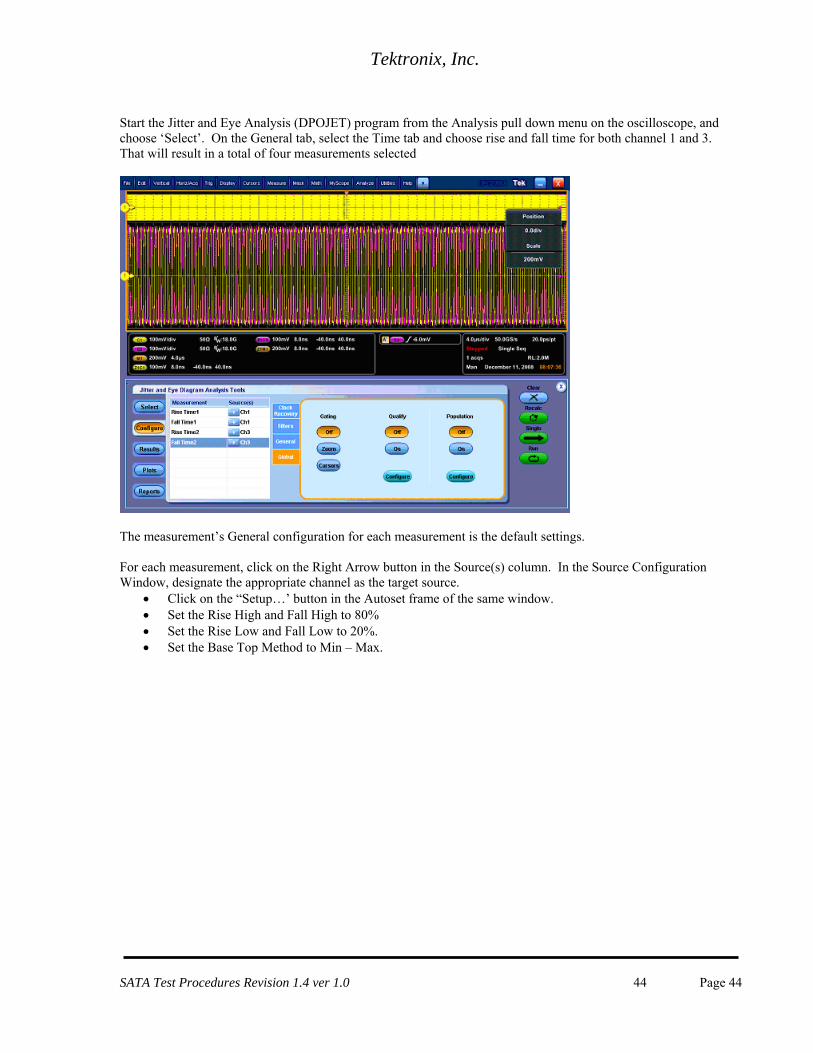
Start the Jitter and Eye Analysis (DPOJET) program from the Analysis pull down menu on the oscilloscope, and choose ‘Select’. On the General tab, select the Time tab and choose rise and fall time for both channel 1 and 3. That will result in a total of four measurements selected
The measurement’s General configuration for each measurement is the default settings. For each measurement, click on the Right Arrow button in the Source(s) column. In the Source Configuration Window, designate the appropriate channel as the target source.
Click on the “Setup…’ button in the Autoset frame of the same window. Set the Rise High and Fall High to 80% Set the Rise Low and Fall Low to 20%. Set the Base Top Method to Min – Max.
SATA Test Procedures Revision 1.4 ver 1.0 44 Page 44
Tektronix, Inc.
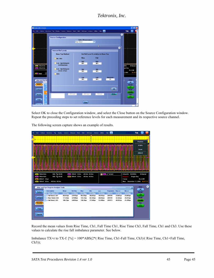
Select OK to close the Configuration window, and select the Close button on the Source Configuration window. Repeat the preceding steps to set reference levels for each measurement and its respective source channel. The following screen capture shows an example of results.
Record the mean values from Rise Time, Ch1, Fall Time Ch1, Rise Time Ch3, Fall Time, Ch1 and Ch3. Use these values to calculate the rise fall imbalance parameter. See below. Imbalance TX+r to TX-f: [%] = 100*ABS(2*( Rise Time, Ch1-Fall Time, Ch3)/( Rise Time, Ch1+Fall Time, Ch3));
SATA Test Procedures Revision 1.4 ver 1.0 45 Page 45
Tektronix, Inc.
Imbalance TX+f to TX-r: [%] = 100*ABS(2*(Fall Time, Ch1-Rise Time, Ch3)/( Fall Time, Ch1+ Rise Time, Ch3)); Note: the imbalance has to be divided by the average of rise and fall time, hence the factor 2 in the equation.
SATA Test Procedures Revision 1.4 ver 1.0 46 Page 46
Tektronix, Inc.
Test TSG-06 - Amplitude Imbalance (Obsolete) Purpose: To verify that the Amplitude Imbalance of the PUT’s transmitter is within the conformance limits. References:
[1] SATA Standard, 7.2.1, Table 29 – Transmitted Signal Requirements [2] Ibid, 7.2.2.3.10 – TX Amplitude Imbalance (Gen2i, Gen1x, Gen2x) [3] SATA Unified Test Document, UTD 1.4
Resource Requirements: See Appendix A. Discussion:
Reference [1] specifies the Transmitted Signal conformance limits for SATA PUTs. This specification includes conformance limits for the TX Amplitude Imbalance. Reference [2] provides the definition of this term for the purposes of SATA testing. Reference [3] defines the measurement requirements for this test. Test Setup:
Connect equipment as shown in Appendix B, figure 1A or 2A as appropriate. Single ended measurements using SMA cables are recommended. Test Procedure:
Using techniques and equipment as described in Appendix A of the PRE-TEST MOI, or equivalent, place the PUT in BISTFIS mode transmitting an HFTP pattern. Depending on the capability of the PUT, and the equipment available, it is acceptable to use either BIST-T or BIST-L to produce the needed test pattern. If the PUT supports disconnects, remove the SATA PRE-TEST system, and connect SATA test fixture. Some PUTs require that the connection not be broken after BIST has been activated. In these situations, it may be necessary to use power splitters to allow simultaneous connection of the PRE-TEST system and the test equipment. Refer to Appendix A of the PRE-TEST MOI for additional details. This test is only performed on Gen2 PUTs. Start the Jitter and Analysis (DPOJET) application on the oscilloscope by selecting it from the Analysis pull down menu. In the Oscilloscope File pull down menu recall SATA_TSG06_G2.set. See the following detailed procedure for additional information. Repeat the PRE-TEST procedure and test for MFTP. Note that for MFTP, only the 2nd bit (non-transition) should be included in the analysis. Test pattern(s): HFTP, MFTP (SSC optional)
SATA usage model: 3.0 Gbps (Gen2i and Gen2m)
Gen2: 4 us/div, 25 ps/pt (> 100,000 UI) Observable Results:
The TX Amplitude Imbalance value shall be less than 10%. Detailed Procedure: Set scope to 100ps/div, 40GSps, 500fs/pt Set scope trigger to CH1, Edge. Adjust trigger level for 0V. Set Horizontal Position to 50%
SATA Test Procedures Revision 1.4 ver 1.0 47 Page 47
Tektronix, Inc.
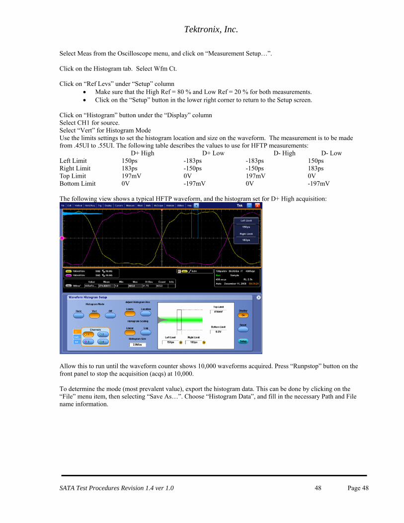
Select Meas from the Oscilloscope menu, and click on “Measurement Setup…”. Click on the Histogram tab. Select Wfm Ct. Click on “Ref Levs” under “Setup” column
Make sure that the High Ref = 80 % and Low Ref = 20 % for both measurements. Click on the “Setup” button in the lower right corner to return to the Setup screen.
Click on “Histogram” button under the “Display” column Select CH1 for source. Select “Vert” for Histogram Mode Use the limits settings to set the histogram location and size on the waveform. The measurement is to be made from .45UI to .55UI. The following table describes the values to use for HFTP measurements: D+ High D+ Low D- High D- Low Left Limit 150ps -183ps -183ps 150ps Right Limit 183ps -150ps -150ps 183ps Top Limit 197mV 0V 197mV 0V Bottom Limit 0V -197mV 0V -197mV The following view shows a typical HFTP waveform, and the histogram set for D+ High acquisition:
Allow this to run until the waveform counter shows 10,000 waveforms acquired. Press “Runpstop” button on the front panel to stop the acquisition (acqs) at 10,000. To determine the mode (most prevalent value), export the histogram data. This can be done by clicking on the “File” menu item, then selecting “Save As…”. Choose “Histogram Data”, and fill in the necessary Path and File name information.
SATA Test Procedures Revision 1.4 ver 1.0 48 Page 48
Tektronix, Inc.
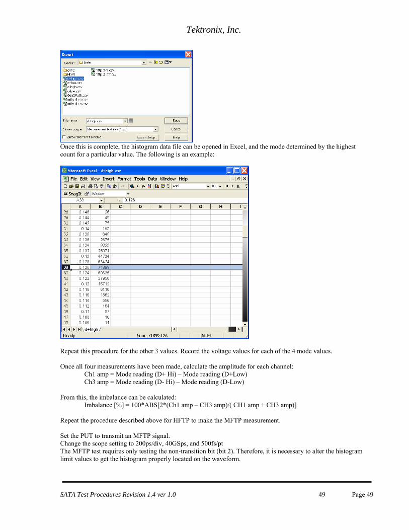
Once this is complete, the histogram data file can be opened in Excel, and the mode determined by the highest count for a particular value. The following is an example:
Repeat this procedure for the other 3 values. Record the voltage values for each of the 4 mode values. Once all four measurements have been made, calculate the amplitude for each channel:
Ch1 amp = Mode reading (D+ Hi) – Mode reading (D+Low) Ch3 amp = Mode reading (D- Hi) – Mode reading (D-Low)
From this, the imbalance can be calculated: Imbalance [%] = 100*ABS[2*(Ch1 amp – CH3 amp)/( CH1 amp + CH3 amp)]
Repeat the procedure described above for HFTP to make the MFTP measurement. Set the PUT to transmit an MFTP signal. Change the scope setting to 200ps/div, 40GSps, and 500fs/pt The MFTP test requires only testing the non-transition bit (bit 2). Therefore, it is necessary to alter the histogram limit values to get the histogram properly located on the waveform.
SATA Test Procedures Revision 1.4 ver 1.0 49 Page 49
Tektronix, Inc.
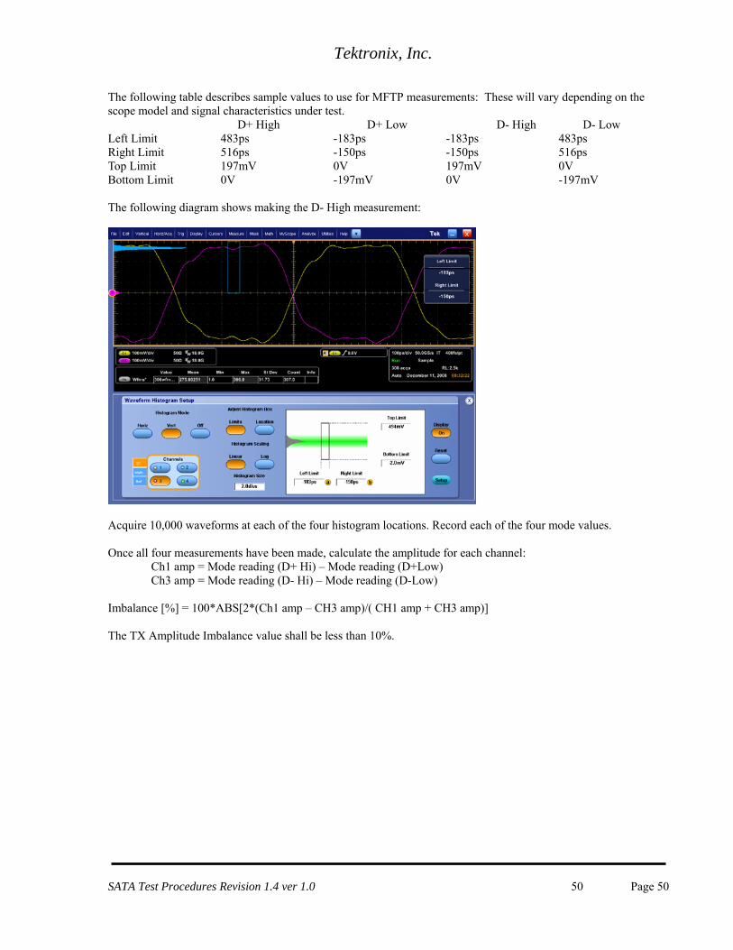
The following table describes sample values to use for MFTP measurements: These will vary depending on the scope model and signal characteristics under test. D+ High D+ Low D- High D- Low Left Limit 483ps -183ps -183ps 483ps Right Limit 516ps -150ps -150ps 516ps Top Limit 197mV 0V 197mV 0V Bottom Limit 0V -197mV 0V -197mV The following diagram shows making the D- High measurement:
Acquire 10,000 waveforms at each of the four histogram locations. Record each of the four mode values. Once all four measurements have been made, calculate the amplitude for each channel:
Ch1 amp = Mode reading (D+ Hi) – Mode reading (D+Low) Ch3 amp = Mode reading (D- Hi) – Mode reading (D-Low)
Imbalance [%] = 100*ABS[2*(Ch1 amp – CH3 amp)/( CH1 amp + CH3 amp)] The TX Amplitude Imbalance value shall be less than 10%.
SATA Test Procedures Revision 1.4 ver 1.0 50 Page 50
Tektronix, Inc.
Test TSG-07 - TJ at Connector, Clock to Data, fBAUD/10 (Obsolete) Purpose: To verify that the TJ at Connector (Clock to Data, fBAUD/10) of the PUT’s transmitter is within the conformance limits. NOTE: This test is no longer required by the SATA Unified Test Document, and per ECN #006. It is provided here as a historical reference. References:
[1] SATA Standard, 7.2.1, Table 22 – Transmitted Signal Requirements [2] Ibid, 7.2.2.3.11 [3] SATA Unified Test Document 1.4
Resource Requirements: See Appendix A. Discussion:
Reference [1] specifies the Transmitted Signal conformance limits for SATA devices. This specification includes conformance limits for the TJ at Connector (Clock to Data, fBAUD/10). Reference [2] provides the definition of this term for the purposes of SATA testing. Reference [3] defines the measurement requirements for this test. Test Setup:
Connect equipment as shown in Appendix B, figure 1 or 2 as appropriate. Note that it is acceptable to use either differential or pseudo-differential (single ended plus math waveform) probes for these measurements. Test Procedure:
Using techniques and equipment as described in Appendix A of the PRE-TEST MOI, or equivalent, place the PUT in BISTFIS mode transmitting an HFTP pattern. Depending on the capability of the PUT, and the equipment available, it is acceptable to use either BIST-T or BIST-L to produce the needed test pattern. If the PUT supports disconnects, remove the SATA PRE-TEST system, and connect SATA test fixture. Some PUTs require that the connection not be broken after BIST has been activated. In these situations, it may be necessary to use power splitters to allow simultaneous connection of the PRE-TEST system and the test equipment. Refer to Appendix A of the PRE-TEST MOI for additional details. Start the Jitter and Analysis (DPOJET) application on the oscilloscope by selecting it from the Analysis pull down menu. In the Oscilloscope File pull down menu, recall the setup: SATA_TSG07_G1.set. For products which support 3Gb/s, this requirement would be tested at 1.5 Gb/s. Repeat PRE-TEST procedure and test using LBP. SSOP is optional. SSC is optional for this test. Test pattern(s): HFTP , LBP , (SSOP is optional) (SSC optional)
SATA usage model: PUTs that support 6.0 and 3.0 Gbps should be tested at 1.5 Gbps for this test
Gen1: 10 us/div, 25 ps/pt (> 100,000 UI) Horizontal scale settings and Record Lengths vary between oscilloscope models, so select the settings that are closest to those specified in this procedure. Observable Results:
NOTE: This test is informative only at this time, and will not affect pass/fail status of PUT.
SATA Test Procedures Revision 1.4 ver 1.0 51 Page 51
Tektronix, Inc.
The TJ at Connector (Clock to Data, fBAUD/10) value shall be less than 0.30 UI for 1.5 Gbps PUTs.
Possible Problems: Per ECN-18, a new LBP pattern was defined that eliminates the disparity ambiguity, as described below. Use ECN-18 compliant LBP for performing the amplitude test whenever possible. If an ECN-18 LBP is not available, it is possible to use the older LBP pattern. However, a pattern mismatch error can occur. To avoid the pattern mismatch problem, make sure that the real lone bit pattern with positive disparity is used (0011 0110 1111 0100 0010 0011 0110 1111 0100 0010 0011 0110 etc….). This pattern has a lone ‘1’ bit between 4 ‘0’s and 3 ‘0’s, and is required for the algorithm. Visually verify the proper disparity on LBP by zooming in on the acquired waveform, and inspecting the waveform for a section that contains a “0001000” section. If this pattern is not readily apparent, re-load the LBP BISTFIS pattern into the PUT, and reacquire the waveform, then repeat the inspection until the proper pattern is seen. Once the proper pattern is detected, continue running the test. It is only necessary to make this inspection on LBP patterns, as there is a 50% chance of getting the desired positive disparity each time the LBP is loaded into the PUT. Detailed Procedure:
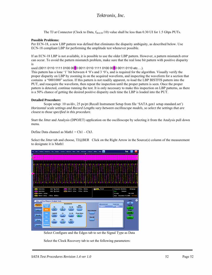
Scope setup: 10 us/div, 25 ps/pt (Recall Instrument Setup from file ‘SATA gen1 setup standard.set’) Horizontal scale settings and Record Lengths vary between oscilloscope models, so select the settings that are closest to those specified in this procedure. Start the Jitter and Analysis (DPOJET) application on the oscilloscope by selecting it from the Analysis pull down menu. Define Data channel as Math1 = Ch1 – Ch3. Select the Jitter tab and choose, TJ@BER Click on the Right Arrow in the Source(s) column of the measurement to designate it is Math1
Select Configure and the Edges tab to set the Signal Type as Data Select the Clock Recovery tab to set the following parameters:
SATA Test Procedures Revision 1.4 ver 1.0 52 Page 52
Tektronix, Inc.
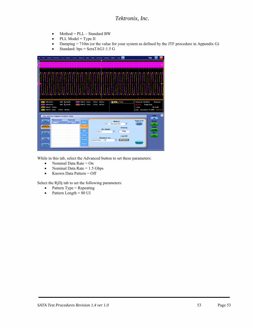
Method = PLL – Standard BW PLL Model = Type II Damping = 710m (or the value for your system as defined by the JTF procedure in Appendix G) Standard: bps = SeraTAG1:1.5 G
While in this tab, select the Advanced button to set these parameters: Nominal Data Rate = On Nominal Data Rate = 1.5 Gbps Known Data Pattern = Off
Select the RjDj tab to set the following parameters: Pattern Type = Repeating Pattern Length = 80 UI
SATA Test Procedures Revision 1.4 ver 1.0 53 Page 53
Tektronix, Inc.
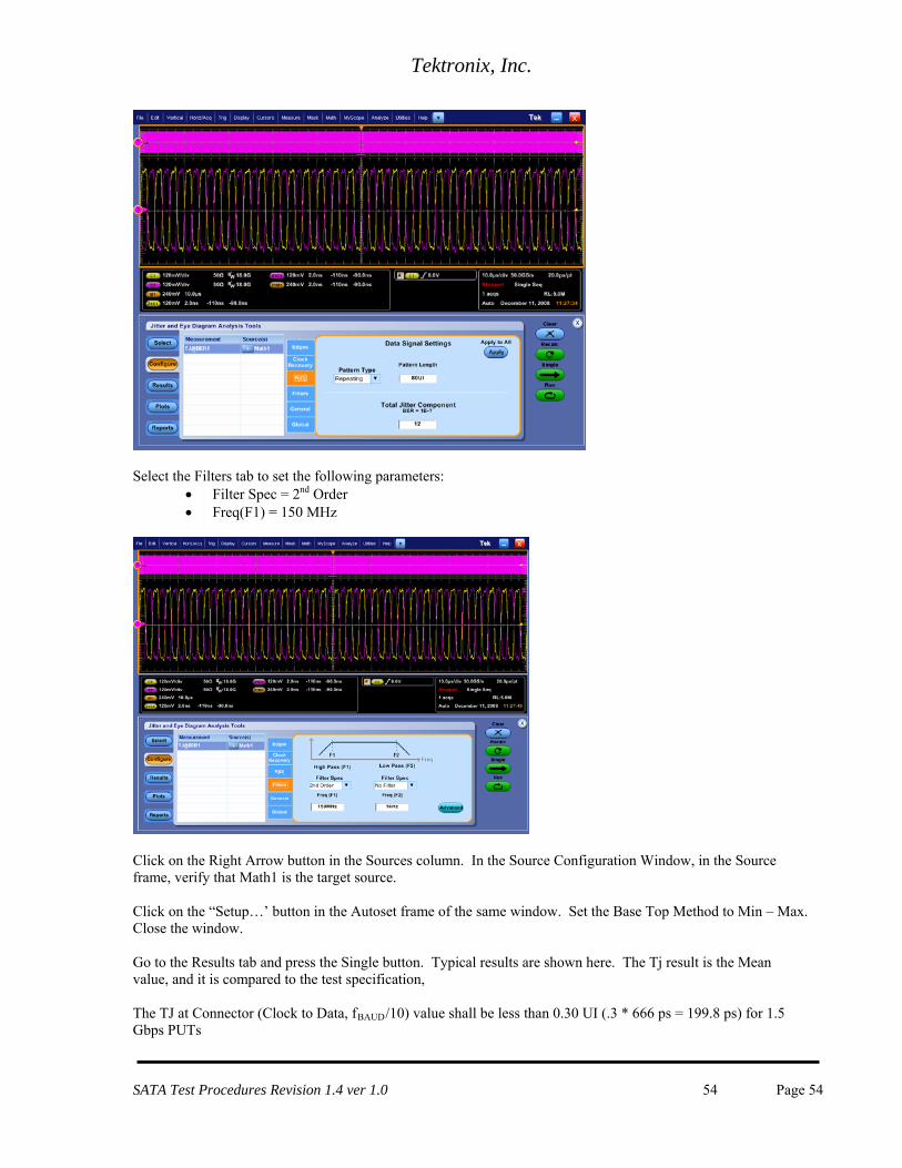
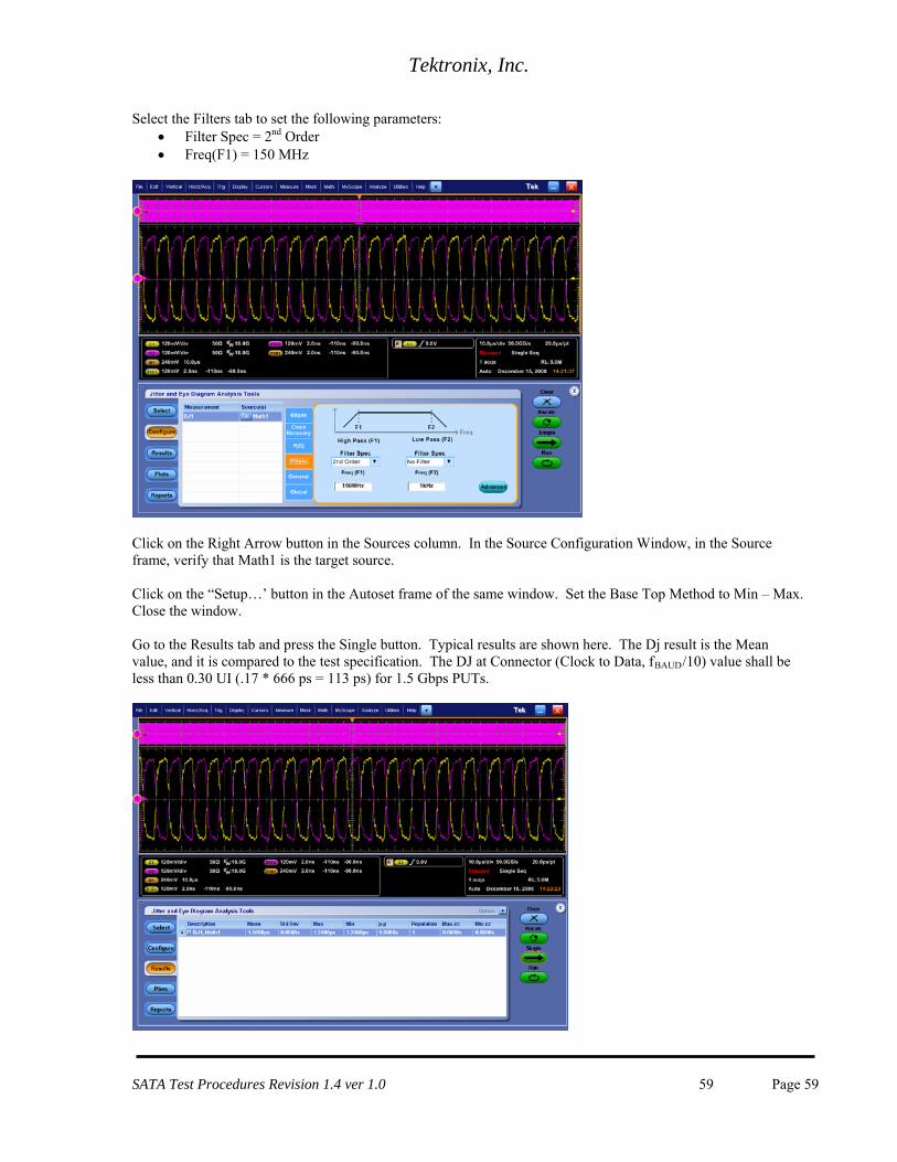
Select the Filters tab to set the following parameters:
Filter Spec = 2nd Order Freq(F1) = 150 MHz
Click on the Right Arrow button in the Sources column. In the Source Configuration Window, in the Source frame, verify that Math1 is the target source. Click on the “Setup…’ button in the Autoset frame of the same window. Set the Base Top Method to Min – Max. Close the window.
Go to the Results tab and press the Single button. Typical results are shown here. The Tj result is the Mean value, and it is compared to the test specification, The TJ at Connector (Clock to Data, fBAUD/10) value shall be less than 0.30 UI (.3 * 666 ps = 199.8 ps) for 1.5 Gbps PUTs
SATA Test Procedures Revision 1.4 ver 1.0 54 Page 54

Tektronix, Inc.
SATA Test Procedures Revision 1.4 ver 1.0 55 Page 55
Tektronix, Inc.
Test TSG-08 - DJ at Connector, Clock to Data, fBAUD/10 (Obsolete) Purpose: To verify that the DJ at Connector (Clock to Data, fBAUD/10) of the PUT’s transmitter is within the conformance limits. NOTE: This test is no longer required by the SATA Unified Test Document, and per ECN #006. It is provided here as a historical reference. References:
[1] SATA Standard, 7.2.1, Table 22 – Transmitted Signal Requirements [2] Ibid, 7.2.2.3.11 [3] SATA Unified Test Document, UTD 1.4
Resource Requirements: See Appendix A. Discussion:
Reference [1] specifies the Transmitted Signal conformance limits for SATA devices. This specification includes conformance limits for the DJ at Connector (Clock to Data, fBAUD/10). Reference [2] provides the definition of this term for the purposes of SATA testing. Reference [3] defines the measurement requirements for this test. This test is informative for all products. Test Setup:
Connect equipment as shown in Appendix B, figure 1 or 2 as appropriate. Note that it is acceptable to use either differential or pseudo-differential (single ended plus math waveform) probes for these measurements. Test Procedure:
Using techniques and equipment as described in Appendix A of the PRE-TEST MOI, or equivalent, place the PUT in BISTFIS mode transmitting an HFTP pattern. Depending on the capability of the PUT, and the equipment available, it is acceptable to use either BIST-T or BIST-L to produce the needed test pattern. If the PUT supports disconnects, remove the SATA PRE-TEST system, and connect SATA test fixture. Some PUTs require that the connection not be broken after BIST has been activated. In these situations, it may be necessary to use power splitters to allow simultaneous connection of the PRE-TEST system and the test equipment. Refer to Appendix A of the PRE-TEST MOI for additional details. Start the Jitter and Analysis (DPOJET) application on the oscilloscope by selecting it from the Analysis pull down menu. In the Oscilloscope File pull down menu, recall the setup: SATA_TSG08_G1.set. This test is only performed on the Gen1 data rate. Repeat PRE-TEST procedure and test using LBP. SSOP is optional. SSC is optional for this test. Test pattern(s): HFTP and LBP. SSOP is optional. (SSC optional)
SATA usage model: 1.5 Gbps (Gen1)
Gen1: 10 us/div, 25 ps/pt (> 100,000 UI) Horizontal scale settings and Record Lengths vary between oscilloscope models, so select the settings that are closest to those specified in this procedure. Observable Results:
SATA Test Procedures Revision 1.4 ver 1.0 56 Page 56
Tektronix, Inc.
NOTE: This test is informative only at this time, and will not affect pass/fail status of PUT. The DJ at Connector (Clock to Data, fBAUD/10) value shall be less than 0.17 UI for 1.5 Gbps PUTs.
Possible Problems:
See LBP discussion in TSG-07 “Possible Problems” section. Detailed Procedure:
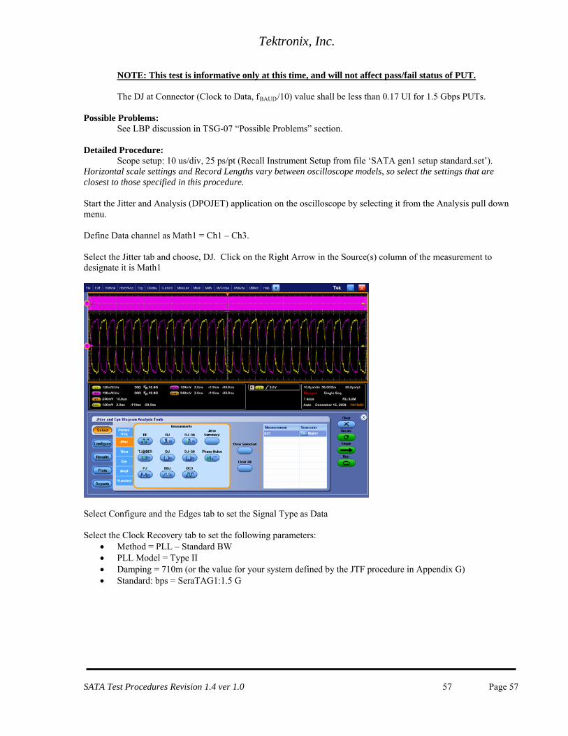
Scope setup: 10 us/div, 25 ps/pt (Recall Instrument Setup from file ‘SATA gen1 setup standard.set’). Horizontal scale settings and Record Lengths vary between oscilloscope models, so select the settings that are closest to those specified in this procedure. Start the Jitter and Analysis (DPOJET) application on the oscilloscope by selecting it from the Analysis pull down menu. Define Data channel as Math1 = Ch1 – Ch3. Select the Jitter tab and choose, DJ. Click on the Right Arrow in the Source(s) column of the measurement to designate it is Math1
Select Configure and the Edges tab to set the Signal Type as Data Select the Clock Recovery tab to set the following parameters:
Method = PLL – Standard BW PLL Model = Type II Damping = 710m (or the value for your system defined by the JTF procedure in Appendix G) Standard: bps = SeraTAG1:1.5 G
SATA Test Procedures Revision 1.4 ver 1.0 57 Page 57

Tektronix, Inc.
While in this tab, select the Advanced button to set these parameters: Nominal Data Rate = On Nominal Data Rate = 1.5 Gbps Known Data Pattern = Off
Select the RjDj tab to set the following parameters:
Pattern Type = Repeating Pattern Length = 80 UI
SATA Test Procedures Revision 1.4 ver 1.0 58 Page 58
Tektronix, Inc.
Select the Filters tab to set the following parameters: Filter Spec = 2nd Order Freq(F1) = 150 MHz
Click on the Right Arrow button in the Sources column. In the Source Configuration Window, in the Source frame, verify that Math1 is the target source. Click on the “Setup…’ button in the Autoset frame of the same window. Set the Base Top Method to Min – Max. Close the window.
Go to the Results tab and press the Single button. Typical results are shown here. The Dj result is the Mean value, and it is compared to the test specification. The DJ at Connector (Clock to Data, fBAUD/10) value shall be less than 0.30 UI (.17 * 666 ps = 113 ps) for 1.5 Gbps PUTs.
SATA Test Procedures Revision 1.4 ver 1.0 59 Page 59
Tektronix, Inc.
Test TSG-09 - Gen1 (1.5 Gb/s) TJ at Connector, Clock to Data, fBAUD/500 Purpose: To verify that the TJ at Connector (Clock to Data, fBAUD/500) of the PUT’s transmitter is within the conformance limits. References:
[1] SATA Standard, 7.2.1, Table 29 – Transmitted Signal Requirements [2] Ibid, 7.2.2.2.18 [3] Ibid, 7.4.8 [4] SATA Unified Test Document, 2.12.9
Resource Requirements: See Appendix A. Last Template Modification: May 15, 2006 (Version 1.0) Discussion:
Reference [1] specifies the Transmitted Signal conformance limits for SATA PUTs. This specification includes conformance limits for the TJ at Connector (Clock to Data, fBAUD/500). Reference [2] provides the definition of this term for the purposes of SATA testing. Reference [3] defines the measurement requirements for this test. Note: This measurement uses a typical Custom Loop Bandwidth equal to the Corner Frequency derived in the Jitter Transfer Function procedure described in Appendix G. Prior to making this jitter measurement, it is necessary to follow the procedure in Appendix G, and determine the proper settings to use for Corner Frequency in DPOJET. The resulting value is recorded in the Loop Bandwidth field in DPOJET for jitter measurements. Test Setup:
Connect equipment as shown in Appendix B, figure 1 or 2 as appropriate. Note that it is acceptable to use either differential or pseudo-differential (single ended plus math waveform) probes for these measurements. Test Procedure: Using techniques and equipment as described in Appendix A of the PRE-TEST MOI, or equivalent, place the PUT in BISTFIS mode transmitting an HFTP pattern. Depending on the capability of the PUT, and the equipment available, it is acceptable to use either BIST-T or BIST-L to produce the needed test pattern. If the PUT supports disconnects, remove the SATA PRE-TEST system, and connect SATA test fixture. Some PUTs require that the connection not be broken after BIST has been activated. In these situations, it may be necessary to use power splitters to allow simultaneous connection of the PRE-TEST system and the test equipment. Refer to Appendix A of the PRE-TEST MOI for additional details. Start the Jitter and Analysis (DPOJET) application on the oscilloscope by selecting it from the Analysis pull down menu. In the Oscilloscope File pull down menu, recall the setup, SATA_TSG09_G1.set For products which support 3Gb/s, this requirement must be tested at 1.5 Gb/s. Repeat PRE-TEST procedure and test using LBP. SSOP is optional. SSC is optional for this test. Test pattern(s): HFTP , LBP , (SSOP is optional) (SSC optional)
SATA usage model: 1.5 Gbps (Gen1)
Gen1: 10 us/div, 25 ps/pt (> 100,000 UI)
SATA Test Procedures Revision 1.4 ver 1.0 60 Page 60
Tektronix, Inc.
Horizontal scale settings and Record Lengths vary between oscilloscope models, so select the settings that are closest to those specified in this procedure. Observable Results: NOTE: This test is informative only at this time, and will not affect pass/fail status of PUT. The TJ at Connector (Clock to Data, fBAUD/10) value shall be less than 0.30 UI for 1.5 Gbps PUTs. Possible Problems: Per ECN-18, a new LBP pattern was defined that eliminates the disparity ambiguity, as described below. Use ECN-18 compliant LBP for performing the amplitude test whenever possible. If an ECN-18 LBP is not available, it is possible to use the older LBP pattern. However, a pattern mismatch error can occur. To avoid the pattern mismatch problem, make sure that the real lone bit pattern with positive disparity is used (0011 0110 1111 0100 0010 0011 0110 1111 0100 0010 0011 0110 etc….). This pattern has a lone ‘1’ bit between 4 ‘0’s and 3 ‘0’s, and is required for the algorithm. Visually verify the proper disparity on LBP by zooming in on the acquired waveform, and inspecting the waveform for a section that contains a “0001000” section. If this pattern is not readily apparent, re-load the LBP BISTFIS pattern into the PUT, and reacquire the waveform, then repeat the inspection until the proper pattern is seen. Once the proper pattern is detected, continue running the test. It is only necessary to make this inspection on LBP patterns, as there is a 50% chance of getting the desired positive disparity each time the LBP is loaded into the PUT. Detailed Procedure: Scope setup: 10 us/div, 25 ps/pt (Recall Instrument Setup from file ‘SATA gen1 setup standard_DJA.set’) Horizontal scale settings and Record Lengths vary between oscilloscope models, so select the settings that are closest to those specified in this procedure. Start the Jitter and Analysis (DPOJET) application on the oscilloscope by selecting it from the Analysis pull down menu. Define Data channel as Math1 = Ch1 – Ch3. Select the Jitter tab and choose, TJ@BER Click on the Right Arrow in the Source(s) column of the measurement to designate it is Math1
SATA Test Procedures Revision 1.4 ver 1.0 61 Page 61

Tektronix, Inc.
Select Configure and the Edges tab to set the Signal Type as Data Select the Clock Recovery tab to set the following parameters:
Method = PLL – Custom BW PLL Model = Type II Damping = The value for your system as defined by the JTF procedure in Appendix G) Loop BW = The corner frequency value for your system as defined by the JTF for procedure in
Appendix G)
While in this tab, select the Advanced button to set these parameters: Nominal Data Rate = On Nominal Data Rate = 1.5 Gbps
SATA Test Procedures Revision 1.4 ver 1.0 62 Page 62
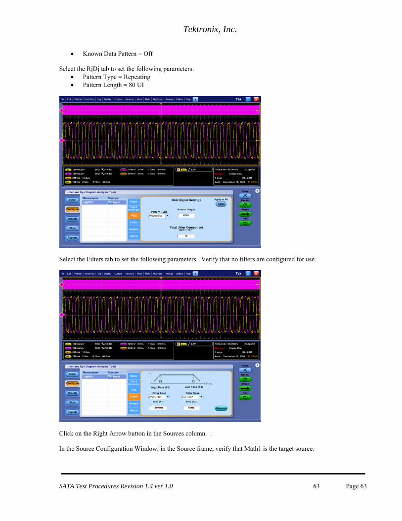
Tektronix, Inc.
Known Data Pattern = Off Select the RjDj tab to set the following parameters:
Pattern Type = Repeating Pattern Length = 80 UI
Select the Filters tab to set the following parameters. Verify that no filters are configured for use.
Click on the Right Arrow button in the Sources column. . In the Source Configuration Window, in the Source frame, verify that Math1 is the target source.
SATA Test Procedures Revision 1.4 ver 1.0 63 Page 63
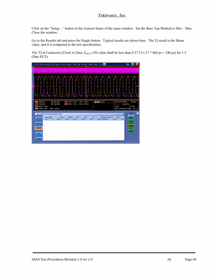
Tektronix, Inc.
Click on the “Setup…’ button in the Autoset frame of the same window. Set the Base Top Method to Min – Max. Close the window.
Go to the Results tab and press the Single button. Typical results are shown here. The Tj result is the Mean value, and it is compared to the test specification, The TJ at Connector (Clock to Data, fBAUD/10) value shall be less than 0.37 UI (.37 * 666 ps = 246 ps) for 1.5 Gbps PUTs
SATA Test Procedures Revision 1.4 ver 1.0 64 Page 64
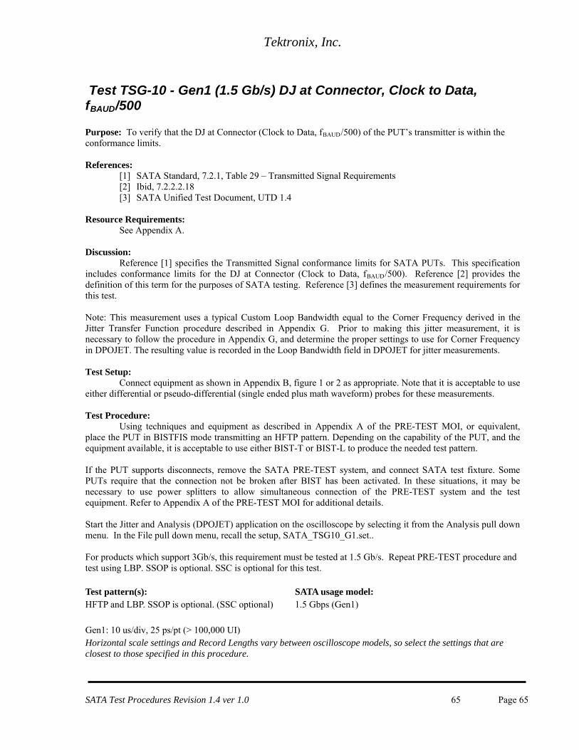
Tektronix, Inc.
Test TSG-10 - Gen1 (1.5 Gb/s) DJ at Connector, Clock to Data, fBAUD/500 Purpose: To verify that the DJ at Connector (Clock to Data, fBAUD/500) of the PUT’s transmitter is within the conformance limits. References:
[1] SATA Standard, 7.2.1, Table 29 – Transmitted Signal Requirements [2] Ibid, 7.2.2.2.18 [3] SATA Unified Test Document, UTD 1.4
Resource Requirements: See Appendix A. Discussion:
Reference [1] specifies the Transmitted Signal conformance limits for SATA PUTs. This specification includes conformance limits for the DJ at Connector (Clock to Data, fBAUD/500). Reference [2] provides the definition of this term for the purposes of SATA testing. Reference [3] defines the measurement requirements for this test. Note: This measurement uses a typical Custom Loop Bandwidth equal to the Corner Frequency derived in the Jitter Transfer Function procedure described in Appendix G. Prior to making this jitter measurement, it is necessary to follow the procedure in Appendix G, and determine the proper settings to use for Corner Frequency in DPOJET. The resulting value is recorded in the Loop Bandwidth field in DPOJET for jitter measurements. Test Setup:
Connect equipment as shown in Appendix B, figure 1 or 2 as appropriate. Note that it is acceptable to use either differential or pseudo-differential (single ended plus math waveform) probes for these measurements. Test Procedure:
Using techniques and equipment as described in Appendix A of the PRE-TEST MOI, or equivalent, place the PUT in BISTFIS mode transmitting an HFTP pattern. Depending on the capability of the PUT, and the equipment available, it is acceptable to use either BIST-T or BIST-L to produce the needed test pattern. If the PUT supports disconnects, remove the SATA PRE-TEST system, and connect SATA test fixture. Some PUTs require that the connection not be broken after BIST has been activated. In these situations, it may be necessary to use power splitters to allow simultaneous connection of the PRE-TEST system and the test equipment. Refer to Appendix A of the PRE-TEST MOI for additional details. Start the Jitter and Analysis (DPOJET) application on the oscilloscope by selecting it from the Analysis pull down menu. In the File pull down menu, recall the setup, SATA_TSG10_G1.set.. For products which support 3Gb/s, this requirement must be tested at 1.5 Gb/s. Repeat PRE-TEST procedure and test using LBP. SSOP is optional. SSC is optional for this test. Test pattern(s): HFTP and LBP. SSOP is optional. (SSC optional)
SATA usage model: 1.5 Gbps (Gen1)
Gen1: 10 us/div, 25 ps/pt (> 100,000 UI) Horizontal scale settings and Record Lengths vary between oscilloscope models, so select the settings that are closest to those specified in this procedure.
SATA Test Procedures Revision 1.4 ver 1.0 65 Page 65
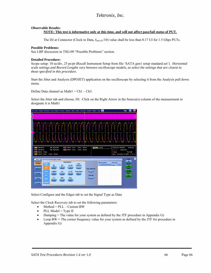
Tektronix, Inc.
Observable Results: NOTE: This test is informative only at this time, and will not affect pass/fail status of PUT. The DJ at Connector (Clock to Data, fBAUD/10) value shall be less than 0.17 UI for 1.5 Gbps PUTs.
Possible Problems: See LBP discussion in TSG-09 “Possible Problems” section. Detailed Procedure: Scope setup: 10 us/div, 25 ps/pt (Recall Instrument Setup from file ‘SATA gen1 setup standard.set’). Horizontal scale settings and Record Lengths vary between oscilloscope models, so select the settings that are closest to those specified in this procedure. Start the Jitter and Analysis (DPOJET) application on the oscilloscope by selecting it from the Analysis pull down menu. Define Data channel as Math1 = Ch1 – Ch3. Select the Jitter tab and choose, DJ. Click on the Right Arrow in the Source(s) column of the measurement to designate it is Math1
Select Configure and the Edges tab to set the Signal Type as Data Select the Clock Recovery tab to set the following parameters:
Method = PLL – Custom BW PLL Model = Type II Damping = The value for your system as defined by the JTF procedure in Appendix G) Loop BW = The corner frequency value for your system as defined by the JTF for procedure in
Appendix G)
SATA Test Procedures Revision 1.4 ver 1.0 66 Page 66
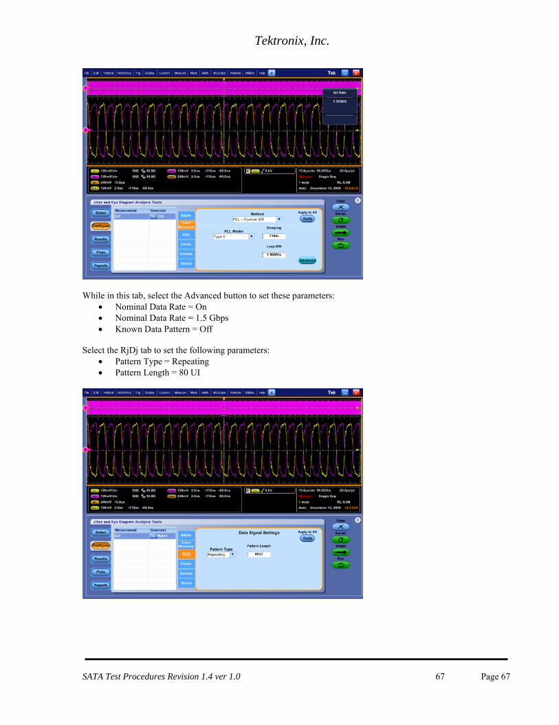
Tektronix, Inc.
While in this tab, select the Advanced button to set these parameters: Nominal Data Rate = On Nominal Data Rate = 1.5 Gbps Known Data Pattern = Off
Select the RjDj tab to set the following parameters:
Pattern Type = Repeating Pattern Length = 80 UI
SATA Test Procedures Revision 1.4 ver 1.0 67 Page 67
Tektronix, Inc.
Select the Filters tab to set the following parameters. Verify that no filters are configured for use.
Go to the Results tab and press the Single button. Typical results are shown here. The Dj result is the Mean value, and it is compared to the test specification, The DJ at Connector (Clock to Data, fBAUD/10) value shall be less than 0.30 UI (.17 * 666 ps = 113 ps) for 1.5 Gbps PUTs
SATA Test Procedures Revision 1.4 ver 1.0 68 Page 68

Tektronix, Inc.
Test TSG-11 - Gen2 (3Gb/s) TJ at Connector, Clock to Data, fBAUD/500 Purpose: To verify that the TJ at Connector (Clock to Data, fBAUD/500) of the PUT’s transmitter is within the conformance limits. References:
[1] SATA Standard, 7.2.1, Table 29 – Transmitted Signal Requirements [2] Ibid, 7.2.2.2.18 [3] SATA Unified Test Document, UTD 1.4
Resource Requirements: See Appendix A. Discussion:
Reference [1] specifies the Transmitted Signal conformance limits for SATA PUTs. This specification includes conformance limits for the TJ at Connector (Clock to Data, fBAUD/500). Reference [2] provides the definition of this term for the purposes of SATA testing. Reference [3] defines the measurement requirements for this test. Note: This measurement uses a typical Custom Loop Bandwidth equal to the Corner Frequency derived in the Jitter Transfer Function procedure described in Appendix G. Prior to making this jitter measurement, it is necessary to follow the procedure in Appendix G, and determine the proper settings to use for Corner Frequency in DPOJET. The resulting value is recorded in the Loop Bandwidth field in DPOJET for jitter measurements. Test Setup:
Connect equipment as shown in Appendix B, figure 1 or 2 as appropriate. Note that it is acceptable to use either differential or pseudo-differential (single ended plus math waveform) probes for these measurements. Test Procedure:
Using techniques and equipment as described in Appendix A of the PRE-TEST MOI, or equivalent, place the PUT in BISTFIS mode transmitting an HFTP pattern. Depending on the capability of the PUT, and the equipment available, it is acceptable to use either BIST-T or BIST-L to produce the needed test pattern. If the PUT supports disconnects, remove the SATA PRE-TEST system, and connect SATA test fixture. Some PUTs require that the connection not be broken after BIST has been activated. In these situations, it may be necessary to use power splitters to allow simultaneous connection of the PRE-TEST system and the test equipment. Refer to Appendix A of the PRE-TEST MOI for additional details. Start the Jitter and Analysis (DPOJET) application on the oscilloscope by selecting it from the Analysis pull down menu. In the Oscilloscope File pull down menu, recall the setup, SATA_TSG11_G2.set. This test is only performed on Gen2 devices. Repeat PRE-TEST procedure and test using LBP. SSOP is optional. SSC is optional for this test. Test pattern(s): HFTP and LBP. SSOP is optional (SSC optional)
SATA usage model: 3.0 Gbps (Gen2i and Gen2m)
Gen2: 4 us/div, 25 ps/pt (> 100,000 UI) Horizontal scale settings and Record Lengths vary between oscilloscope models, so select the settings that are closest to those specified in this procedure. Observable Results:
SATA Test Procedures Revision 1.4 ver 1.0 69 Page 69
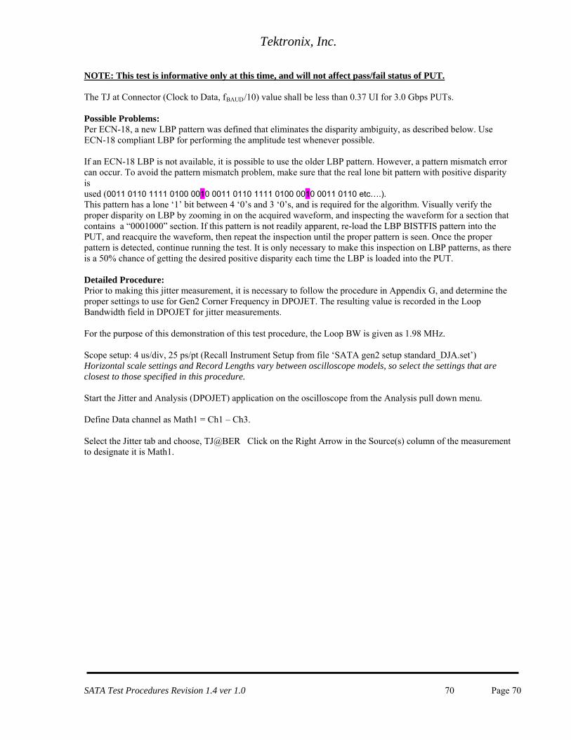
Tektronix, Inc.
NOTE: This test is informative only at this time, and will not affect pass/fail status of PUT. The TJ at Connector (Clock to Data, fBAUD/10) value shall be less than 0.37 UI for 3.0 Gbps PUTs. Possible Problems: Per ECN-18, a new LBP pattern was defined that eliminates the disparity ambiguity, as described below. Use ECN-18 compliant LBP for performing the amplitude test whenever possible. If an ECN-18 LBP is not available, it is possible to use the older LBP pattern. However, a pattern mismatch error can occur. To avoid the pattern mismatch problem, make sure that the real lone bit pattern with positive disparity is used (0011 0110 1111 0100 0010 0011 0110 1111 0100 0010 0011 0110 etc….). This pattern has a lone ‘1’ bit between 4 ‘0’s and 3 ‘0’s, and is required for the algorithm. Visually verify the proper disparity on LBP by zooming in on the acquired waveform, and inspecting the waveform for a section that contains a “0001000” section. If this pattern is not readily apparent, re-load the LBP BISTFIS pattern into the PUT, and reacquire the waveform, then repeat the inspection until the proper pattern is seen. Once the proper pattern is detected, continue running the test. It is only necessary to make this inspection on LBP patterns, as there is a 50% chance of getting the desired positive disparity each time the LBP is loaded into the PUT. Detailed Procedure: Prior to making this jitter measurement, it is necessary to follow the procedure in Appendix G, and determine the proper settings to use for Gen2 Corner Frequency in DPOJET. The resulting value is recorded in the Loop Bandwidth field in DPOJET for jitter measurements. For the purpose of this demonstration of this test procedure, the Loop BW is given as 1.98 MHz. Scope setup: 4 us/div, 25 ps/pt (Recall Instrument Setup from file ‘SATA gen2 setup standard_DJA.set’) Horizontal scale settings and Record Lengths vary between oscilloscope models, so select the settings that are closest to those specified in this procedure. Start the Jitter and Analysis (DPOJET) application on the oscilloscope from the Analysis pull down menu. Define Data channel as Math1 = Ch1 – Ch3. Select the Jitter tab and choose, TJ@BER Click on the Right Arrow in the Source(s) column of the measurement to designate it is Math1.
SATA Test Procedures Revision 1.4 ver 1.0 70 Page 70
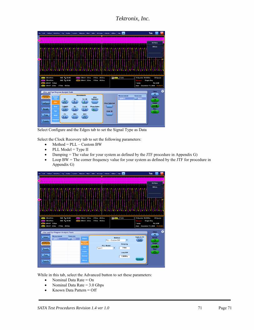
Tektronix, Inc.
Select Configure and the Edges tab to set the Signal Type as Data Select the Clock Recovery tab to set the following parameters:
Method = PLL – Custom BW PLL Model = Type II Damping = The value for your system as defined by the JTF procedure in Appendix G) Loop BW = The corner frequency value for your system as defined by the JTF for procedure in
Appendix G)
While in this tab, select the Advanced button to set these parameters: Nominal Data Rate = On Nominal Data Rate = 3.0 Gbps Known Data Pattern = Off
SATA Test Procedures Revision 1.4 ver 1.0 71 Page 71
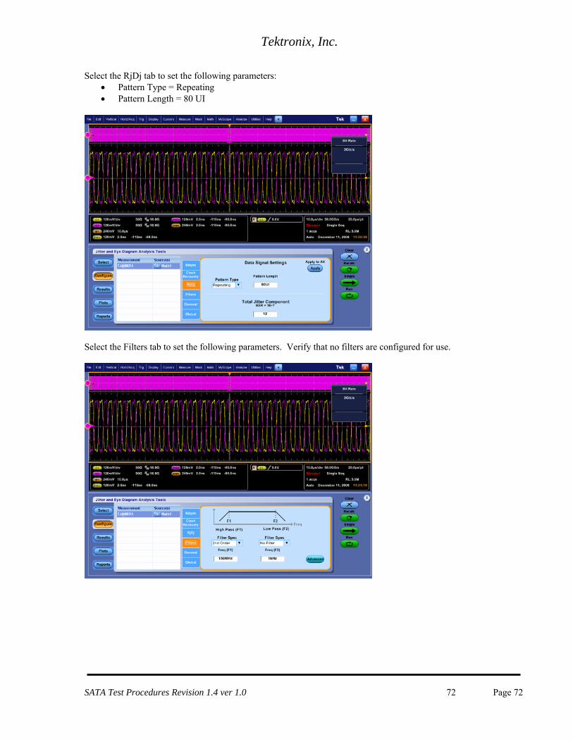
Tektronix, Inc.
Select the RjDj tab to set the following parameters: Pattern Type = Repeating Pattern Length = 80 UI
Select the Filters tab to set the following parameters. Verify that no filters are configured for use.
SATA Test Procedures Revision 1.4 ver 1.0 72 Page 72
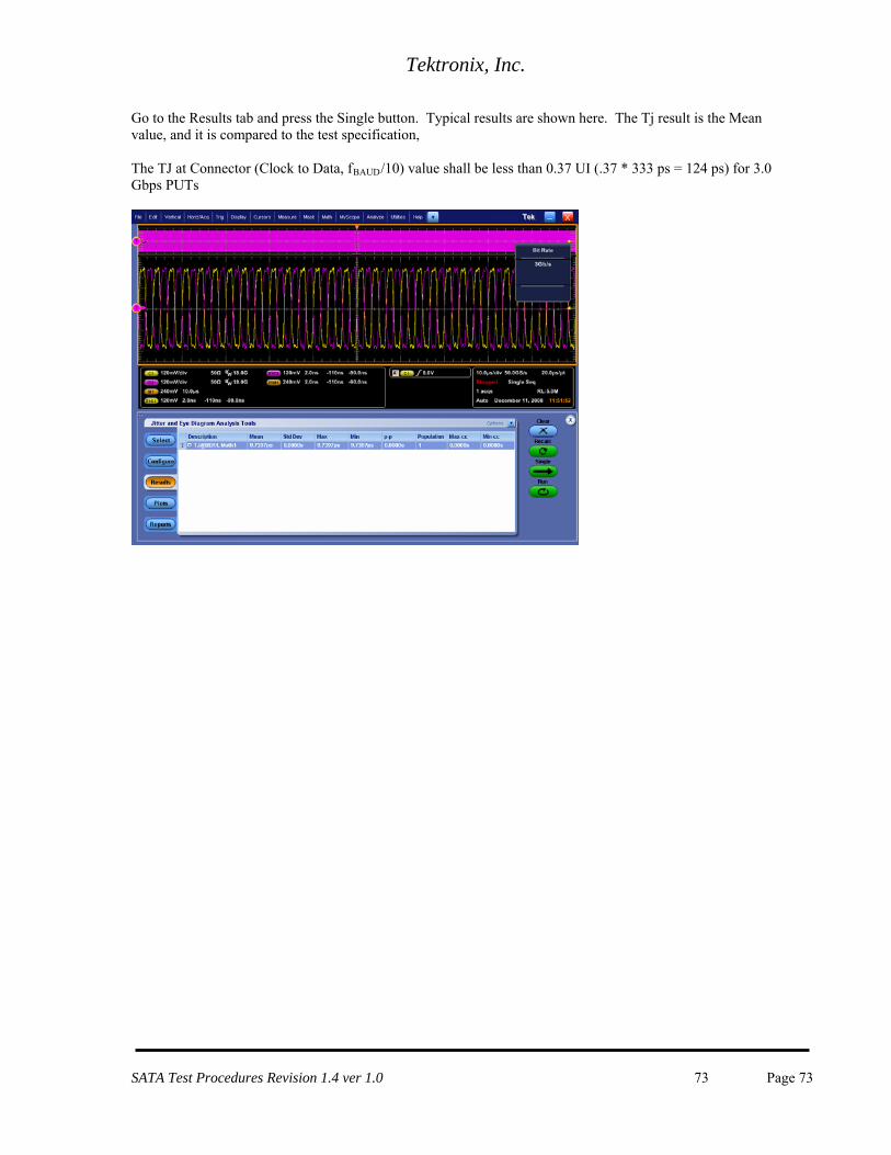
Tektronix, Inc.
Go to the Results tab and press the Single button. Typical results are shown here. The Tj result is the Mean value, and it is compared to the test specification, The TJ at Connector (Clock to Data, fBAUD/10) value shall be less than 0.37 UI (.37 * 333 ps = 124 ps) for 3.0 Gbps PUTs
SATA Test Procedures Revision 1.4 ver 1.0 73 Page 73
Tektronix, Inc.
Test TSG-12 - Gen2 (3Gb/s) DJ at Connector, Clock to Data, fBAUD/500 Purpose: To verify that the DJ at Connector (Clock to Data, fBAUD/500) of the PUT’s transmitter is within the conformance limits. References:
[1] SATA Standard, 7.2.1, Table 29 – Transmitted Signal Requirements [2] Ibid, 7.2.2.2.18 [3] SATA Unified Test Document, UTD 1.4
Resource Requirements: See Appendix A. Discussion:
Reference [1] specifies the Transmitted Signal conformance limits for SATA PUTs. This specification includes conformance limits for the DJ at Connector (Clock to Data, fBAUD/500). Reference [2] provides the definition of this term for the purposes of SATA testing. Reference [3] defines the measurement requirements for this test. Note: This measurement uses a typical Custom Loop Bandwidth equal to the Corner Frequency derived in the Jitter Transfer Function procedure described in Appendix G. Prior to making this jitter measurement, it is necessary to follow the procedure in Appendix G, and determine the proper settings to use for Corner Frequency in DPOJET. The resulting value is recorded in the Loop Bandwidth field in DPOJET for jitter measurements. Test Setup:
Connect equipment as shown in Appendix B, figure 1 or 2 as appropriate. Note that it is acceptable to use either differential or pseudo-differential (single ended plus math waveform) probes for these measurements. Test Procedure:
Using techniques and equipment as described in Appendix A of the PRE-TEST MOI, or equivalent, place the PUT in BISTFIS mode transmitting an HFTP pattern. Depending on the capability of the PUT, and the equipment available, it is acceptable to use either BIST-T or BIST-L to produce the needed test pattern. If the PUT supports disconnects, remove the SATA PRE-TEST system, and connect SATA test fixture. Some PUTs require that the connection not be broken after BIST has been activated. In these situations, it may be necessary to use power splitters to allow simultaneous connection of the PRE-TEST system and the test equipment. Refer to Appendix A of the PRE-TEST MOI for additional details. This test is only performed on Gen2 devices. Repeat PRE-TEST procedure and test using LBP. SSOP is optional. SSC is optional for this test. Start the Jitter and Analysis (DPOJET) application on the oscilloscope by selecting it from the Analysis pull down menu. In the File pull down menu, recall the setup, SATA_TSG12_G2.set.
Test pattern(s): HFTP and LBP, (SSOP is optional) (SSC optional)
SATA usage model: 3.0 Gbps (Gen2i and Gen2m)
Gen2: 4 us/div, 25 ps/pt (> 100,000 UI) Horizontal scale settings and Record Lengths vary between oscilloscope models, so select the settings that are closest to those specified in this procedure.
SATA Test Procedures Revision 1.4 ver 1.0 74 Page 74
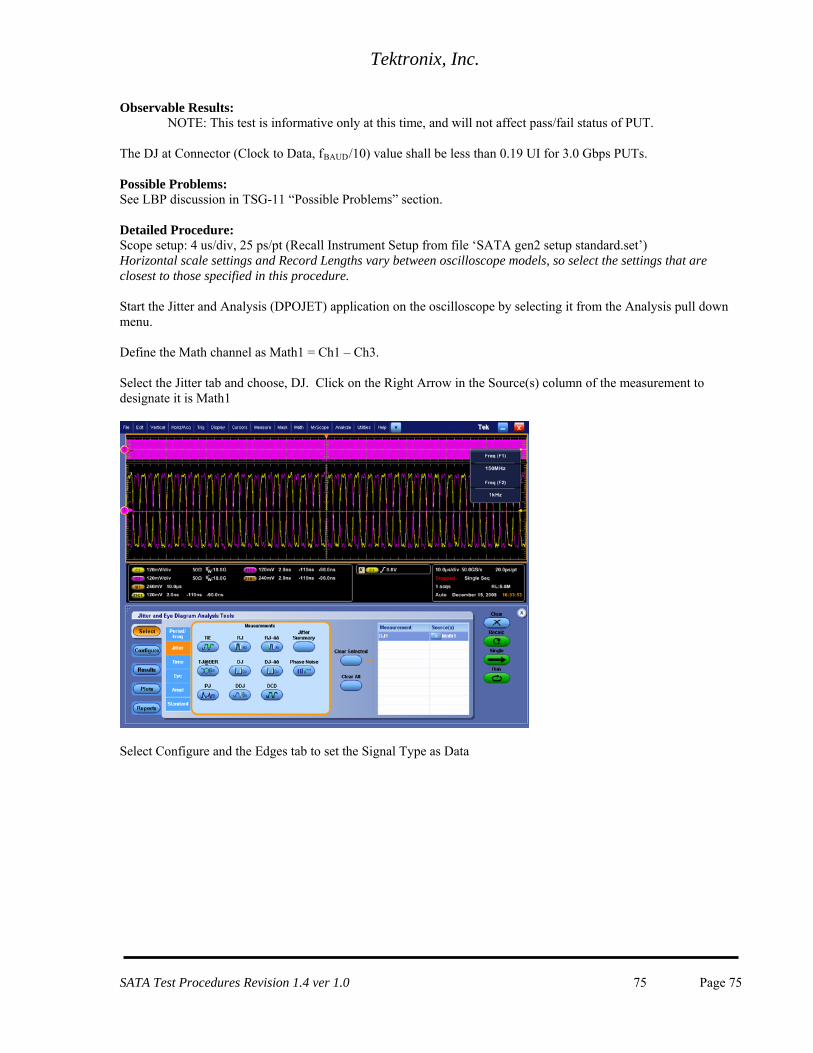
Tektronix, Inc.
Observable Results: NOTE: This test is informative only at this time, and will not affect pass/fail status of PUT.
The DJ at Connector (Clock to Data, fBAUD/10) value shall be less than 0.19 UI for 3.0 Gbps PUTs. Possible Problems: See LBP discussion in TSG-11 “Possible Problems” section. Detailed Procedure: Scope setup: 4 us/div, 25 ps/pt (Recall Instrument Setup from file ‘SATA gen2 setup standard.set’) Horizontal scale settings and Record Lengths vary between oscilloscope models, so select the settings that are closest to those specified in this procedure. Start the Jitter and Analysis (DPOJET) application on the oscilloscope by selecting it from the Analysis pull down menu. Define the Math channel as Math1 = Ch1 – Ch3. Select the Jitter tab and choose, DJ. Click on the Right Arrow in the Source(s) column of the measurement to designate it is Math1
Select Configure and the Edges tab to set the Signal Type as Data
SATA Test Procedures Revision 1.4 ver 1.0 75 Page 75

Tektronix, Inc.
Select the Clock Recovery tab to set the following parameters: Method = PLL – Custom BW PLL Model = Type II Damping = The value for your system as defined by the JTF procedure in Appendix G) Loop BW = The corner frequency value for your system as defined by the JTF for procedure in
Appendix G)
While in this tab, select the Advanced button to set these parameters: Nominal Data Rate = On Nominal Data Rate = 3.0 Gbps Known Data Pattern = Off
SATA Test Procedures Revision 1.4 ver 1.0 76 Page 76
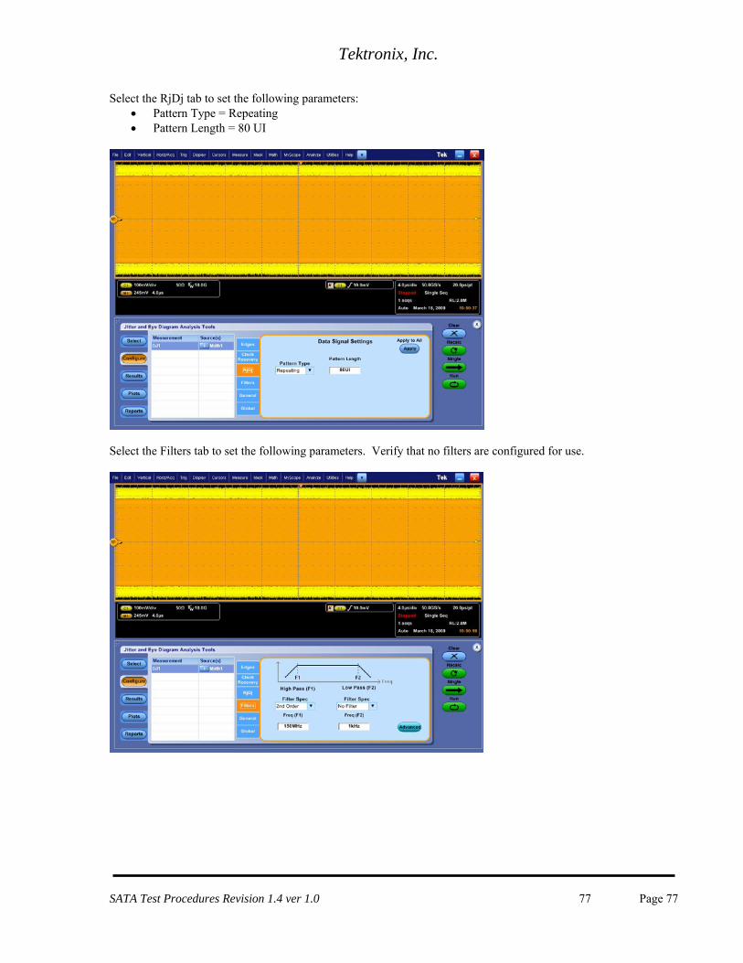
Tektronix, Inc.
Select the RjDj tab to set the following parameters: Pattern Type = Repeating Pattern Length = 80 UI
Select the Filters tab to set the following parameters. Verify that no filters are configured for use.
SATA Test Procedures Revision 1.4 ver 1.0 77 Page 77
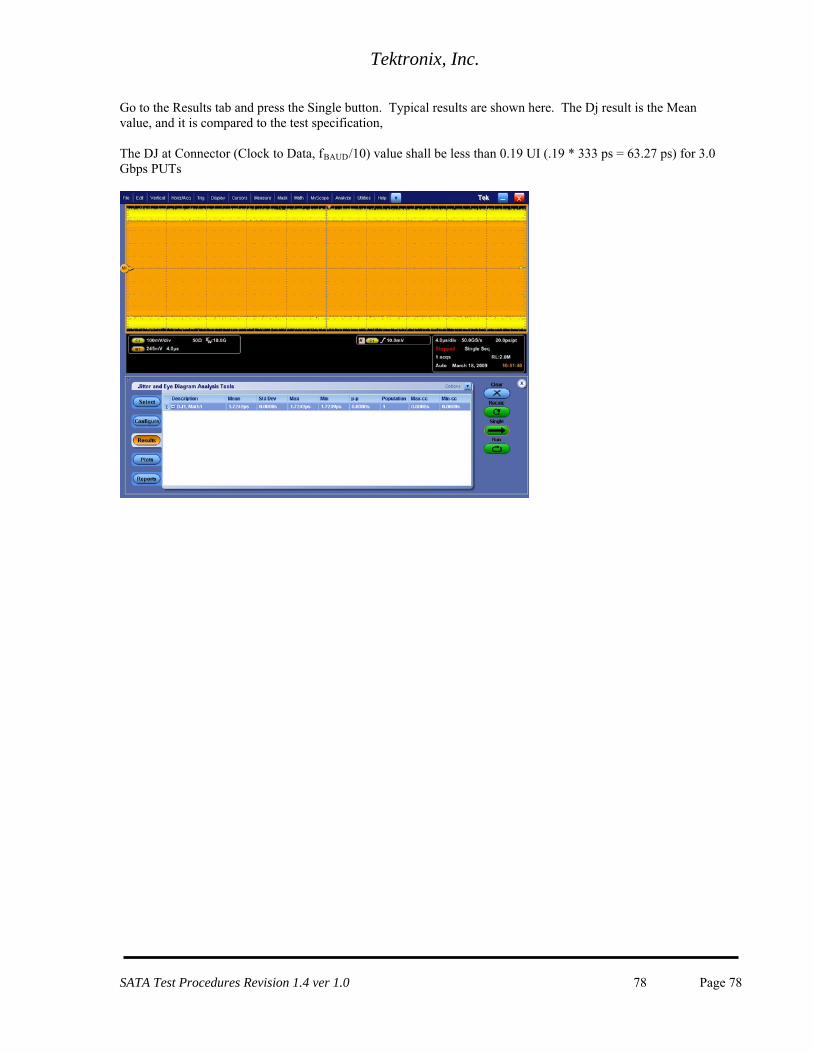
Tektronix, Inc.
Go to the Results tab and press the Single button. Typical results are shown here. The Dj result is the Mean value, and it is compared to the test specification, The DJ at Connector (Clock to Data, fBAUD/10) value shall be less than 0.19 UI (.19 * 333 ps = 63.27 ps) for 3.0 Gbps PUTs
SATA Test Procedures Revision 1.4 ver 1.0 78 Page 78
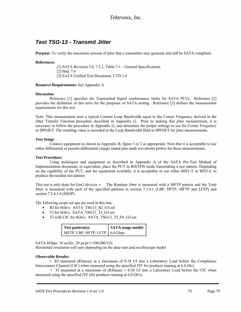
Tektronix, Inc.
Test TSG-13 - Transmit Jitter Purpose: To verify the maximum amount of jitter that a transmitter may generate and still be SATA compliant. References:
[1] SATA Revision 3.0, 7.2.1, Table 7-1 – General Specifications [2] Ibid, 7.4 [3] SATA Unified Test Document, UTD 1.4
Resource Requirements: See Appendix A Discussion:
Reference [1] specifies the Transmitted Signal conformance limits for SATA PUTs. Reference [2] provides the definition of this term for the purposes of SATA testing. Reference [3] defines the measurement requirements for this test.
Note: This measurement uses a typical Custom Loop Bandwidth equal to the Corner Frequency derived in the Jitter Transfer Function procedure described in Appendix G. Prior to making this jitter measurement, it is necessary to follow the procedure in Appendix G, and determine the proper settings to use for Corner Frequency in DPOJET. The resulting value is recorded in the Loop Bandwidth field in DPOJET for jitter measurements. Test Setup:
Connect equipment as shown in Appendix B, figure 1 or 2 as appropriate. Note that it is acceptable to use either differential or pseudo-differential (single ended plus math waveform) probes for these measurements. Test Procedure:
Using techniques and equipment as described in Appendix A of the SATA Pre-Test Method of Implementation document, or equivalent, place the PUT in BISTFIS mode transmitting a test pattern. Depending on the capability of the PUT, and the equipment available, it is acceptable to use either BIST-T or BIST-L to produce the needed test pattern. This test is only done for Gen3 devices. • The Random Jitter is measured with a MFTP pattern and the Total Jitter is measured with each of the specified patterns in section 7.2.4.1 (LBP, HFTP, MFTP and LFTP) and section 7.2.4.3.4 (SSOP). The following scope set-ups are used in this test.
RJ for 6Gb/s: SATA_TSG13_RJ_G3.set TJ for 6Gb/s: SATA_TSG13_TJ_G3.set TJ with CIC for 6Gb/s: SATA_TSG13_TJ_Flt_G3.set
Test pattern(s): MFTP, LBP, HFTP, LFTP
SATA usage model: 6.0 Gbps
SATA 6Gbps: 10 us/div, 20 ps/pt (>100,000 UI). Horizontal resolution will vary depending on the data rate and oscilloscope model Observable Results:
• RJ measured (RJmeas) at a maximum of 0.18 UI into a Laboratory Load before the Compliance Interconnect Channel (CIC) when measured using the specified JTF for products running at 6.0 Gb/s
• TJ measured at a maximum of (RJmeas) + 0.34 UI into a Laboratory Load before the CIC when measured using the specified JTF (for products running at 6.0 Gb/s)
SATA Test Procedures Revision 1.4 ver 1.0 79 Page 79
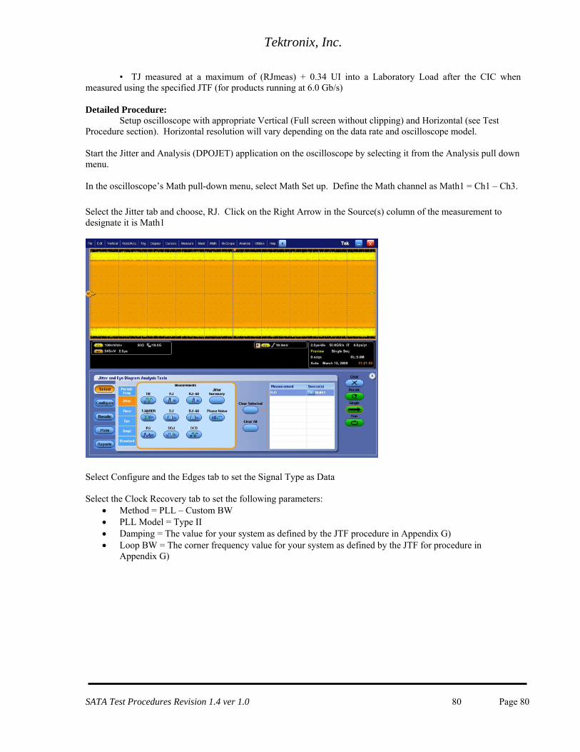
Tektronix, Inc.
• TJ measured at a maximum of (RJmeas) + 0.34 UI into a Laboratory Load after the CIC when measured using the specified JTF (for products running at 6.0 Gb/s) Detailed Procedure:
Setup oscilloscope with appropriate Vertical (Full screen without clipping) and Horizontal (see Test Procedure section). Horizontal resolution will vary depending on the data rate and oscilloscope model.
Start the Jitter and Analysis (DPOJET) application on the oscilloscope by selecting it from the Analysis pull down menu. In the oscilloscope’s Math pull-down menu, select Math Set up. Define the Math channel as Math1 = Ch1 – Ch3. Select the Jitter tab and choose, RJ. Click on the Right Arrow in the Source(s) column of the measurement to designate it is Math1
Select Configure and the Edges tab to set the Signal Type as Data Select the Clock Recovery tab to set the following parameters:
Method = PLL – Custom BW PLL Model = Type II Damping = The value for your system as defined by the JTF procedure in Appendix G) Loop BW = The corner frequency value for your system as defined by the JTF for procedure in
Appendix G)
SATA Test Procedures Revision 1.4 ver 1.0 80 Page 80

Tektronix, Inc.
While in this tab, select the Advanced button to set these parameters:
Nominal Data Rate = On Nominal Data Rate = 6.0 Gbps Known Data Pattern = Off
Select the RjDj tab to set the following parameters:
Pattern Type = Repeating Pattern Length = 80 UI
Go to the Results tab and press the Single button. Typical results are shown here.
SATA Test Procedures Revision 1.4 ver 1.0 81 Page 81

Tektronix, Inc.
Read the Random Mean jitter component value as the RJ value. Calculate: Rj(Pk-Pk) = 14 * RJ1 (For reference to this formula, see Section 7.3.4 Jitter Budget in SATA specification) Verify that the value is not greater than .18 UI (.18 *166 ps = 29.88 ps) for a 6.0 Gbps device. The next section of the procedure is dedicated to testing TJ before and after CIC. Clk-Data for SATA 6Gbps
Test Procedure:
Using techniques and equipment as described in Appendix A of the SATA Pre-Test Method of Implementation document, or equivalent, place the PUT in BISTFIS mode transmitting an LBP pattern. Depending on the capability of the PUT, and the equipment available, it is acceptable to use either BIST-T or BIST-L to produce the needed test pattern. This is only done for Gen3 devices.
Test pattern(s): LBP, HFTP, MFTP, LFTP
SATA usage model: 6.0 Gbps
SATA 6Gbps: 2 us/div, 20 ps/pt (>100,000 UI) Horizontal scale settings and Record Lengths vary between oscilloscope models, so select the settings that are closest to those specified in this procedure Observable Results: The TJ before and after CIC. Clk-Data for SATA 6Gbps shall not be greater than the measured RJ (Pk-Pk) value [from TSG 14] + 0.34 UI (166 ps * 0.34 =56.44 ps) for a 6.0 Gbps device. Refer to Section 7.4.10 in the SATA specification for the definition of the Tj budget. Detailed Procedure: Setup oscilloscope with appropriate Vertical (Full screen without clipping) and Horizontal (see Test Procedure section). Horizontal resolution will vary depending on the data rate and oscilloscope model.
SATA Test Procedures Revision 1.4 ver 1.0 82 Page 82
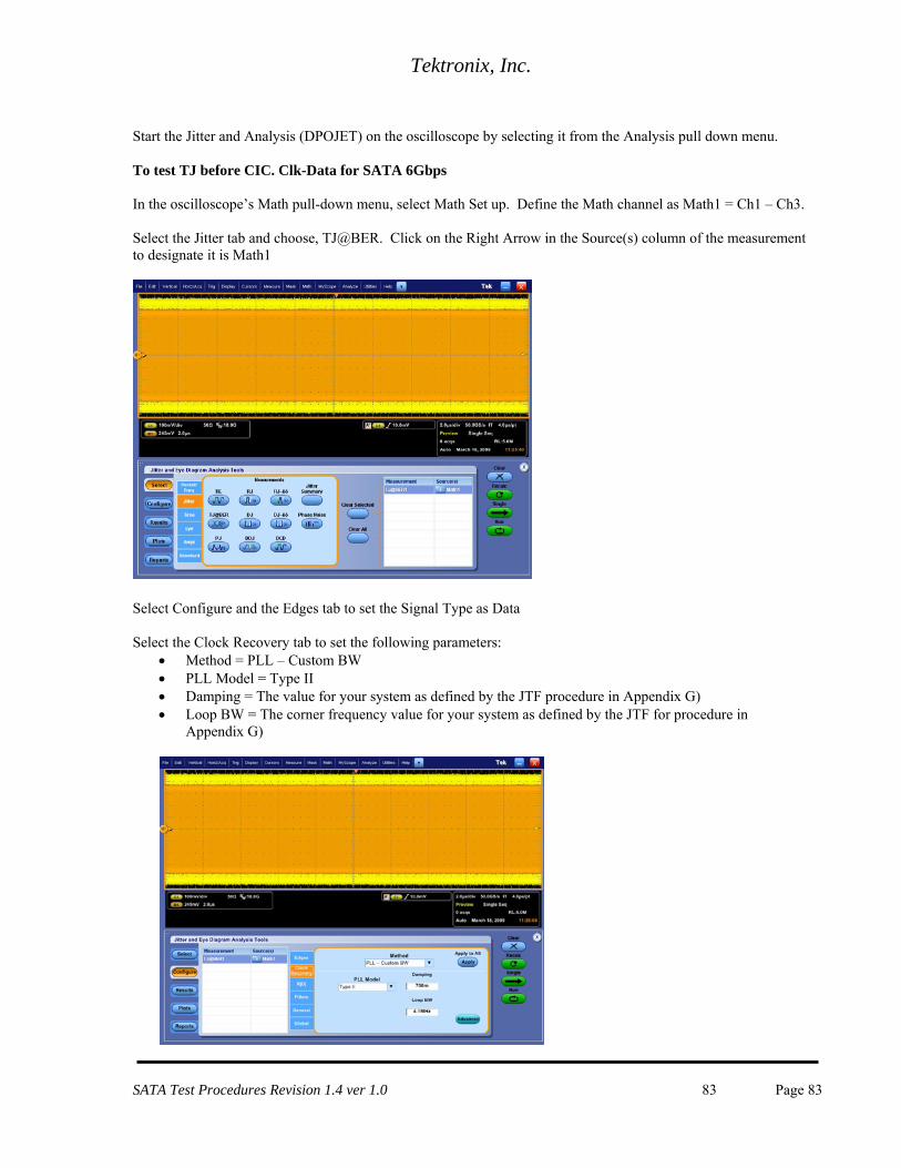
Tektronix, Inc.
Start the Jitter and Analysis (DPOJET) on the oscilloscope by selecting it from the Analysis pull down menu. To test TJ before CIC. Clk-Data for SATA 6Gbps In the oscilloscope’s Math pull-down menu, select Math Set up. Define the Math channel as Math1 = Ch1 – Ch3. Select the Jitter tab and choose, TJ@BER. Click on the Right Arrow in the Source(s) column of the measurement to designate it is Math1
Select Configure and the Edges tab to set the Signal Type as Data Select the Clock Recovery tab to set the following parameters:
Method = PLL – Custom BW PLL Model = Type II Damping = The value for your system as defined by the JTF procedure in Appendix G) Loop BW = The corner frequency value for your system as defined by the JTF for procedure in
Appendix G)
SATA Test Procedures Revision 1.4 ver 1.0 83 Page 83
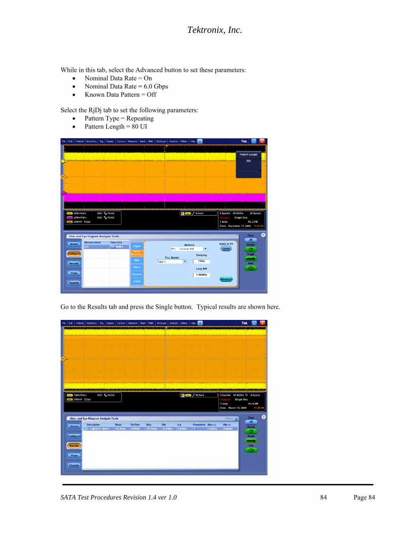
Tektronix, Inc.
While in this tab, select the Advanced button to set these parameters:
Nominal Data Rate = On Nominal Data Rate = 6.0 Gbps Known Data Pattern = Off
Select the RjDj tab to set the following parameters:
Pattern Type = Repeating Pattern Length = 80 UI
Go to the Results tab and press the Single button. Typical results are shown here.
SATA Test Procedures Revision 1.4 ver 1.0 84 Page 84
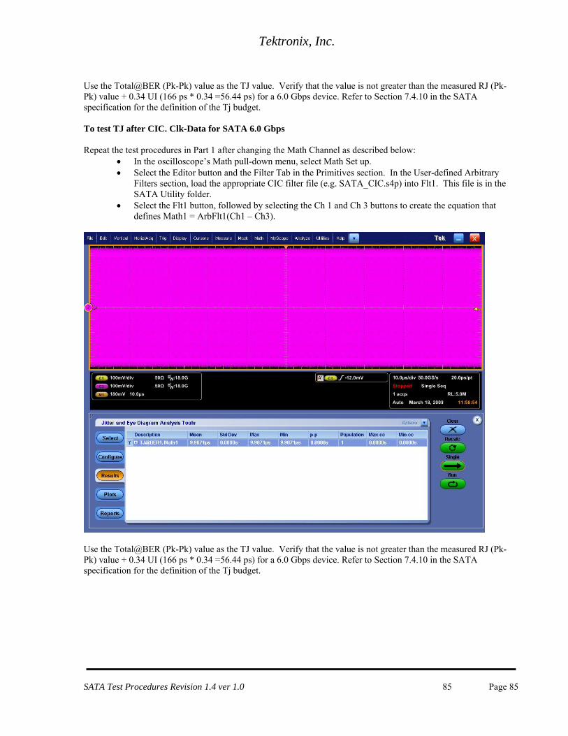
Tektronix, Inc.
Use the Total@BER (Pk-Pk) value as the TJ value. Verify that the value is not greater than the measured RJ (Pk-Pk) value + 0.34 UI (166 ps * 0.34 =56.44 ps) for a 6.0 Gbps device. Refer to Section 7.4.10 in the SATA specification for the definition of the Tj budget. To test TJ after CIC. Clk-Data for SATA 6.0 Gbps Repeat the test procedures in Part 1 after changing the Math Channel as described below:
In the oscilloscope’s Math pull-down menu, select Math Set up. Select the Editor button and the Filter Tab in the Primitives section. In the User-defined Arbitrary
Filters section, load the appropriate CIC filter file (e.g. SATA_CIC.s4p) into Flt1. This file is in the SATA Utility folder.
Select the Flt1 button, followed by selecting the Ch 1 and Ch 3 buttons to create the equation that defines Math1 = ArbFlt1(Ch1 – Ch3).
Use the Total@BER (Pk-Pk) value as the TJ value. Verify that the value is not greater than the measured RJ (Pk-Pk) value + 0.34 UI (166 ps * 0.34 =56.44 ps) for a 6.0 Gbps device. Refer to Section 7.4.10 in the SATA specification for the definition of the Tj budget.
SATA Test Procedures Revision 1.4 ver 1.0 85 Page 85
Tektronix, Inc.
Test TSG-14: - TX Maximum Differential Output Voltage Amplitude (Gen3i) Purpose: The differential voltage [(TX+) – (TX-)] measured at the Transmitter shall comply with the respective electrical specifications of section 7.2. References:
[1] SATA Standard, 7.2.1, Table 7-3 – Transmitted Signal Requirements [2] Ibid, 7.4.3.2 – Minimum Differential Voltage Amplitude (Gen3i) [3] SATA Unified Test Document, UTD 1.4
Resource Requirements: See Appendix A Discussion:
Reference [1] specifies the Transmitted Signal conformance limits for SATA PUTs. This specification includes conformance limits for the Minimum Differential Voltage Amplitude. Reference [2] provides the definition of this term for the purposes of SATA testing. Reference [3] defines the measurement requirements for this test.
Test Setup:
Connect equipment as shown in Appendix B, figure 1 or 2 as appropriate. Note that it is acceptable to use either differential or pseudo-differential (single ended plus math waveform) probes for these measurements. Test Procedure:
Using techniques and equipment as described in Appendix A of the PRE-TEST MOI, or equivalent, place the PUT in BISTFIS mode transmitting an MFTP pattern. Depending on the capability of the PUT, and the equipment available, it is acceptable to use either BIST-T or BIST-L to produce the needed test pattern. If the PUT supports disconnects, remove the SATA PRE-TEST system, and connect SATA test fixture. Some PUTs require that the connection not be broken after BIST has been activated. In these situations, it may be necessary to use power splitters to allow simultaneous connection of the PRE-TEST system and the test equipment. Refer to Appendix A of the PRE-TEST MOI for additional details. In the File pull down menu, recall the setup, SATA_TSG14_G3.set. Start DPOJET to capture the waveform. When the required waveform is displayed on the oscilloscope, the differential MFTP signal is captured in a time span for each waveform encompassing more than four Gen3 unit intervals (4 x 166.6 ps). The Peak-to-Peak Amplitude over a 4UI epoch, for a minimum of 500 acquisitions (2000 UI) time averaged waveforms. Test pattern(s): MFTP
SATA usage model: 6.0 Gbps (Gen3i)
Gen3: 250ps/div, 2 ps/pt (> 2,000 UI) Horizontal scale settings and Record Lengths vary between oscilloscope models, so select the settings that are closest to those specified in this procedure. Observable Results:
The differential voltage [(TX+) – (TX-)] measured at the Transmitter shall comply with the respective electrical specifications of section 7.2 of the SATA specification
Max 900 mvppd
SATA Test Procedures Revision 1.4 ver 1.0 86 Page 86
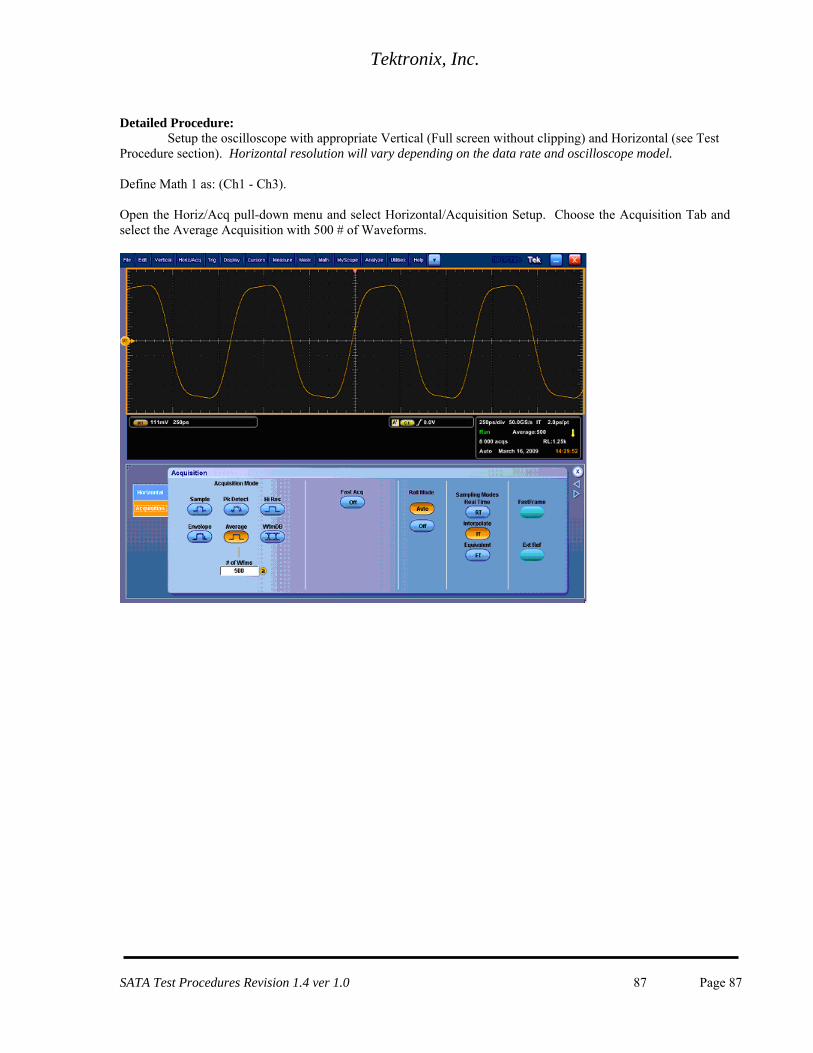
Tektronix, Inc.
Detailed Procedure:
Setup the oscilloscope with appropriate Vertical (Full screen without clipping) and Horizontal (see Test Procedure section). Horizontal resolution will vary depending on the data rate and oscilloscope model. Define Math 1 as: (Ch1 - Ch3). Open the Horiz/Acq pull-down menu and select Horizontal/Acquisition Setup. Choose the Acquisition Tab and select the Average Acquisition with 500 # of Waveforms.
SATA Test Procedures Revision 1.4 ver 1.0 87 Page 87

Tektronix, Inc.
Open the Measure pull-down menu and select Measurement Setup. Choose a Peak to Peak measurement on the Source, Math1 (M1).
The result of the Mean value shall comply with the respective electrical specifications of section 7.2 of the SATA specification
Max 900 mvppd
SATA Test Procedures Revision 1.4 ver 1.0 88 Page 88

Tektronix, Inc.
Test TSG-15: - TX Minimum Differential Output Voltage Amplitude (Gen3i) Purpose: To verify that the Differential Output Voltage of the PUT’s transmitter is within the conformance limits for Gen3 (6.0 Gbps) PUTs. References:
[4] SATA Standard, 7.2.1, Table 7-3 – Transmitted Signal Requirements [5] Ibid, 7.4.3.2 – Minimum Differential Voltage Amplitude (Gen3i) [6] SATA Unified Test Document, UTD 1.4
Resource Requirements: See Appendix A Discussion:
Reference [1] specifies the Transmitted Signal conformance limits for SATA PUTs. This specification includes conformance limits for the Minimum Differential Voltage Amplitude. Reference [2] provides the definition of this term for the purposes of SATA testing. Reference [3] defines the measurement requirements for this test.
Test Setup:
Connect equipment as shown in Appendix B, figure 1 or 2 as appropriate. Note that it is acceptable to use either differential or pseudo-differential (single ended plus math waveform) probes for these measurements. Test Procedure:
Using techniques and equipment as described in Appendix A of the PRE-TEST MOI, or equivalent, place the PUT in BISTFIS mode transmitting an LBP pattern. Depending on the capability of the PUT, and the equipment available, it is acceptable to use either BIST-T or BIST-L to produce the needed test pattern. If the PUT supports disconnects, remove the SATA PRE-TEST system, and connect SATA test fixture. Some PUTs require that the connection not be broken after BIST has been activated. In these situations, it may be necessary to use power splitters to allow simultaneous connection of the PRE-TEST system and the test equipment. Refer to Appendix A of the PRE-TEST MOI for additional details. In the File pull down menu, recall the setup, SATA_TSG15_G3.set. Note: This measurement uses a typical Custom Loop Bandwidth equal to the Corner Frequency derived in the Jitter Transfer Function procedure described in Appendix G. Prior to making this jitter measurement, it is necessary to follow the procedure in Appendix G, and determine the proper settings to use for Corner Frequency in DPOJET. The resulting value is recorded in the Loop Bandwidth field in DPOJET for jitter measurements. Start DPOJET to capture the waveform using the Gen3i Reference Clock JTF for 6 Gbps devices. When the required waveform is displayed on the oscilloscope, a filter is applied to create a Math waveform. A measurement is taken of the High and Low amplitude values of the middle of the eye opening of the resulting signal. The results are fitted into into linear plots (e.g. Transformation Q) which are extrapolated out to 1E^-12 BER. The difference between High and Low amplitudes at 1E^-12 BER are evaluated and compared to the Pass/Fail Criteria (Table 7-3 of Serial ATA Revision 3.0) Test pattern(s): LBP (SSC optional)
SATA usage model: 6.0 Gbps (Gen3i)
Gen3: 1us/div, RL: 500K, 50 GS/s, 20 ps/pt (> 100,000 UI)
SATA Test Procedures Revision 1.4 ver 1.0 89 Page 89
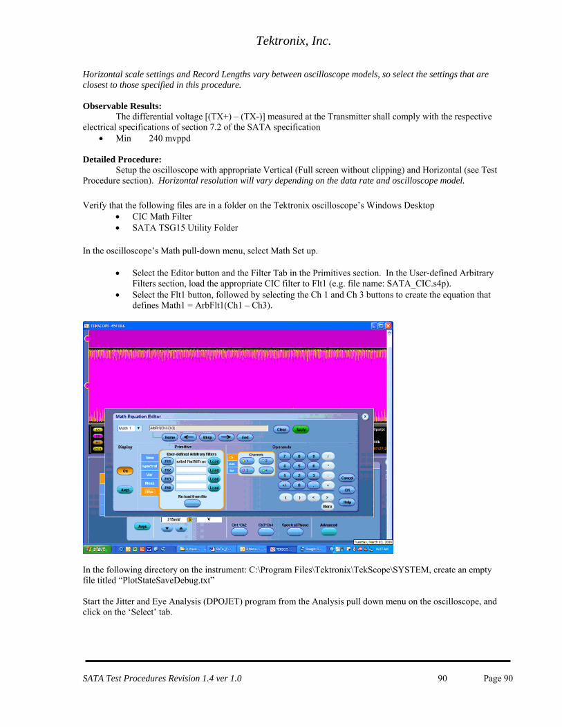
Tektronix, Inc.
Horizontal scale settings and Record Lengths vary between oscilloscope models, so select the settings that are closest to those specified in this procedure. Observable Results:
The differential voltage [(TX+) – (TX-)] measured at the Transmitter shall comply with the respective electrical specifications of section 7.2 of the SATA specification
Min 240 mvppd Detailed Procedure:
Setup the oscilloscope with appropriate Vertical (Full screen without clipping) and Horizontal (see Test Procedure section). Horizontal resolution will vary depending on the data rate and oscilloscope model.
Verify that the following files are in a folder on the Tektronix oscilloscope’s Windows Desktop
CIC Math Filter SATA TSG15 Utility Folder
In the oscilloscope’s Math pull-down menu, select Math Set up.
Select the Editor button and the Filter Tab in the Primitives section. In the User-defined Arbitrary Filters section, load the appropriate CIC filter to Flt1 (e.g. file name: SATA_CIC.s4p).
Select the Flt1 button, followed by selecting the Ch 1 and Ch 3 buttons to create the equation that defines Math1 = ArbFlt1(Ch1 – Ch3).
In the following directory on the instrument: C:\Program Files\Tektronix\TekScope\SYSTEM, create an empty file titled “PlotStateSaveDebug.txt” Start the Jitter and Eye Analysis (DPOJET) program from the Analysis pull down menu on the oscilloscope, and click on the ‘Select’ tab.
SATA Test Procedures Revision 1.4 ver 1.0 90 Page 90
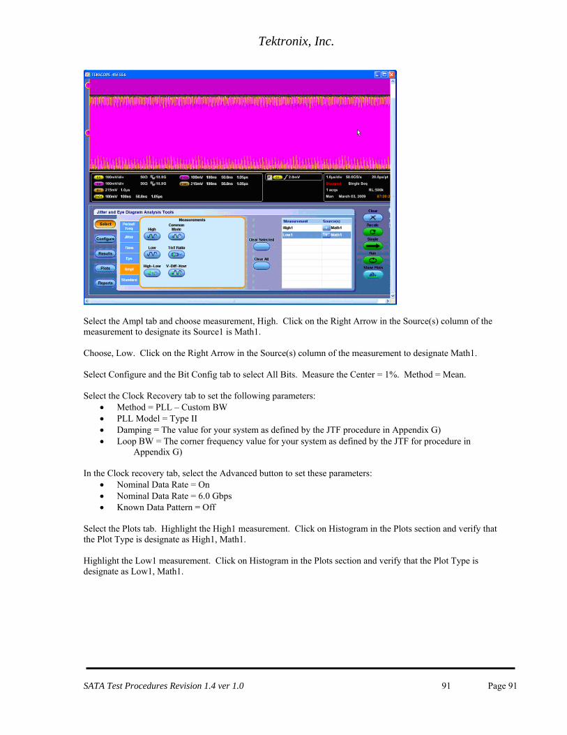
Tektronix, Inc.
Select the Ampl tab and choose measurement, High. Click on the Right Arrow in the Source(s) column of the measurement to designate its Source1 is Math1. Choose, Low. Click on the Right Arrow in the Source(s) column of the measurement to designate Math1. Select Configure and the Bit Config tab to select All Bits. Measure the Center = 1%. Method = Mean. Select the Clock Recovery tab to set the following parameters:
Method = PLL – Custom BW PLL Model = Type II Damping = The value for your system as defined by the JTF procedure in Appendix G) Loop BW = The corner frequency value for your system as defined by the JTF for procedure in
Appendix G) In the Clock recovery tab, select the Advanced button to set these parameters:
Nominal Data Rate = On Nominal Data Rate = 6.0 Gbps Known Data Pattern = Off
Select the Plots tab. Highlight the High1 measurement. Click on Histogram in the Plots section and verify that the Plot Type is designate as High1, Math1. Highlight the Low1 measurement. Click on Histogram in the Plots section and verify that the Plot Type is designate as Low1, Math1.
SATA Test Procedures Revision 1.4 ver 1.0 91 Page 91
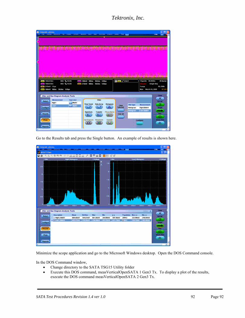
Tektronix, Inc.
Go to the Results tab and press the Single button. An example of results is shown here.
Minimize the scope application and go to the Microsoft Windows desktop. Open the DOS Command console. In the DOS Command window,
Change directory to the SATA TSG15 Utility folder Execute this DOS command, measVerticalOpenSATA 1 Gen3 Tx. To display a plot of the results,
execute the DOS command measVerticalOpenSATA 2 Gen3 Tx.
SATA Test Procedures Revision 1.4 ver 1.0 92 Page 92
Tektronix, Inc.
A summary of the results will be displayed. Record the value labeled as “Minimum Differential Voltage Amplitude at BER 10^-12”. This value shall comply with the respective electrical specifications of section 7.2 of the specification.
Min 240 mvppd
SATA Test Procedures Revision 1.4 ver 1.0 93 Page 93
Tektronix, Inc.
Test TSG-16 - TX AC Common Mode Voltage (Gen3i) Purpose: To verify that the AC Common Mode Voltage of the PUT’s transmitter is within the conformance limits for SATA Gen3i (6.0 Gbps). References:
[1] SATA Standard, 7.2.1, Table 29 – Transmitted Signal Requirements [2] Ibid, 7.2.2.3.5 – TX AC Common Mode Voltage (Gen3i) [3] SATA Unified Test Document, UTD 1.4
Resource Requirements: See Appendix A. Discussion:
Reference [1] specifies the Transmitted Signal conformance limits for SATA PUTs. This specification includes conformance limits for the TX AC Common Mode Voltage. Reference [2] provides the definition of this term for the purposes of SATA testing. Reference [3] defines the measurement requirements for this test. Test Setup:
Connect equipment as shown in Appendix B, figure 1A or 2A as appropriate. Note that it is only acceptable to use two single ended SMA connections for these measurements. Test Procedure:
Using techniques and equipment as described in Appendix A of the PRE-TEST MOI, or equivalent, place the PUT in BISTFIS mode transmitting an HFTP pattern. Depending on the capability of the PUT, and the equipment available, it is acceptable to use either BIST-T or BIST-L to produce the needed test pattern. If the PUT supports disconnects, remove the SATA PRE-TEST system, and connect SATA test fixture. Some PUTs require that the connection not be broken after BIST has been activated. In these situations, it may be necessary to use power splitters to allow simultaneous connection of the PRE-TEST system and the test equipment. Refer to Appendix A of the PRE-TEST MOI for additional details. For SATA Gen3 PUTs (6.0 Gbps), Refer to the detailed procedure in the section below. This is only done for Gen3 PUTs. Testing with SSC is optional. In the File pull down menu, recall the setup, SATA_TSG16_G3.set. Start the scope application and recall the setup ‘SATA gen3 TX AC CM V.set”. See the detailed procedure which follows.
Test pattern(s): HFTP
SATA usage model: 6.0 Gbps
SATA 6Gbps: 2.0 ns/div, 20.0 ps/pt (>100,000 UI) Horizontal scale settings and Record Lengths vary between oscilloscope models, so select the settings that are closest to those specified in this procedure. Observable Results:
The TX AC Common Mode Voltage frequency value shall be lower than 26 dB and 30 dB, respectively at the 3 GHz and 6 GHz frequencies for 6Gbps devices. Detailed Procedure:
Press the Default Set up button followed by the Autoset button on the console. Configure the oscilloscope with the settings below for this measurement.
SATA Test Procedures Revision 1.4 ver 1.0 94 Page 94
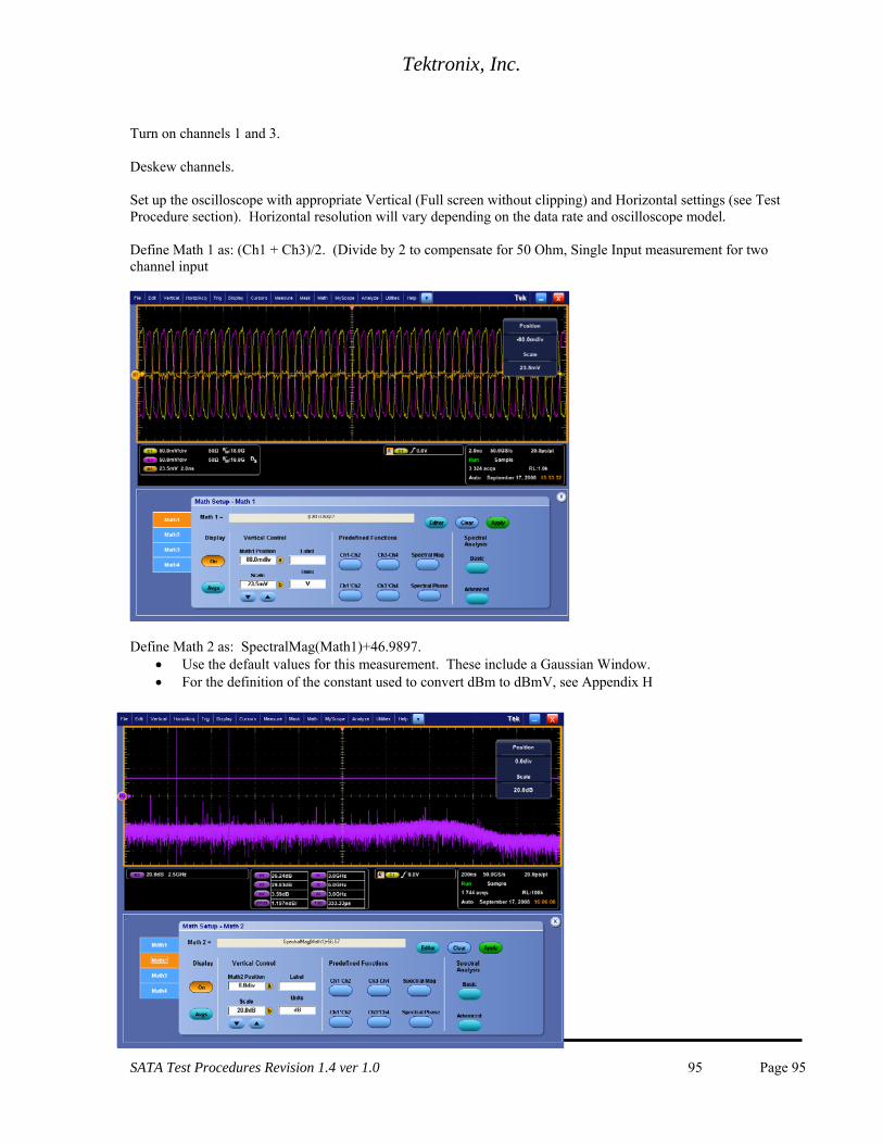
Tektronix, Inc.
SATA Test Procedures Revision 1.4 ver 1.0 95 Page 95
Turn on channels 1 and 3. Deskew channels. Set up the oscilloscope with appropriate Vertical (Full screen without clipping) and Horizontal settings (see Test Procedure section). Horizontal resolution will vary depending on the data rate and oscilloscope model. Define Math 1 as: (Ch1 + Ch3)/2. (Divide by 2 to compensate for 50 Ohm, Single Input measurement for two channel input
Define Math 2 as: SpectralMag(Math1)+46.9897.
Use the default values for this measurement. These include a Gaussian Window. For the definition of the constant used to convert dBm to dBmV, see Appendix H
Tektronix, Inc.
The TX AC Common Mode Voltage frequency value shall be lower than 26 dB and 30 dB, respectively at the 3 GHz and 6 GHz frequencies for 6Gbps devices. The vertical cursor X1 marks 3 GHz and the spur at this point shall be no higher than cursor Y1 which marks 26 dB. The vertical cursor X2 marks 6 GHz and the spur at this point shall be no higher than cursor Y2 which marks 30 dB.
SATA Test Procedures Revision 1.4 ver 1.0 96 Page 96
Tektronix, Inc.
PHY OOB REQUIREMENTS (OOB 1-7)
Overview: This group of tests verifies the Phy OOB Requirements, as defined in Section 2.17 of the SATA Interoperability Unified Test Document, v1.4 (which references the SATA Standard, v3.0).
SATA Test Procedures Revision 1.4 ver 1.0 97 Page 97
Tektronix, Inc.
Test OOB-01 – OOB Signal Detection Threshold Purpose: To verify that the OOB Signal Detection Threshold of the PUT’s receiver is within the conformance limits. References:
[1] SATA Standard, 7.2.1, Table 32 – OOB Specifications [2] Ibid, 7.2.2.7.1 [3] Ibid, 7.4.20 [4] SATA unified test document, 2.14.1
Resource Requirements: See appendix A. See Appendix F for AWG7102 Amplitude Calibration procedure that is required to be performed prior to running the OOB-01 test. Last Template Modification: May 15, 2006 (Version 1.0) Discussion:
Reference [1] specifies the Transmitted Signal conformance limits for SATA PUTs. This specification includes conformance limits for the OOB Signal Detection Threshold. Reference [2] provides the definition of this term for the purposes of SATA testing. Reference [3] defines the measurement requirements for this test. Test Setup:
Observe the setup outlined in Appendix C. If using the AWG7102, connect CH1 Analog outputs to PUT receiver inputs. Connect CH1 MKR1 to scope CH4. If using the AWG710, connect Marker 1 output to PUT Rx+, Marker 2 output to PUT Rx-, and Marker 2 BAR to scope CH4.
Set the scope to 200us/div, 1.25GS/s, and 800ps/pt. Set scope CH1 and CH3 to 50mV/div. Set Math
waveform to Ch1-Ch3, and set math gain to 200mV/div. These settings can automatically be set by recalling the “SATA oob” setup file. Connect scope CH1 and CH3 to the PUT Tx+ and Tx- respectively. Test Procedure: Note: The same test patterns are used to test both Gen1 and Gen2 PUTs. Per the SATA specification, the OOB signaling is performed only at 1.5 Gbps. However, the SATA specification calls for different minimum amplitude for this test between Gen1 and Gen2 PUTs, as described in the following procedure.
For PUTs running at both at 1.5 Gbps and 3.0 Gpbs, perform the following tests:
Load test pattern crst02-3G210.awg (compliance com-reset) on the AWG. This file sets the AWG to the required 210mV output amplitude using the COMRESET pattern. Verify that the PUT provides a stable response (valid detection) to the OOB signal from the AWG, as illustrated in the figures below. There should be a response from the PUT to every COMINIT/COMRESET and COMWAKE pair from the AWG, across the entire 2ms acquisition. Any missing COMWAKEs will appear as gaps in the 2ms record, and should be considered a failure.
SATA Test Procedures Revision 1.4 ver 1.0 98 Page 98
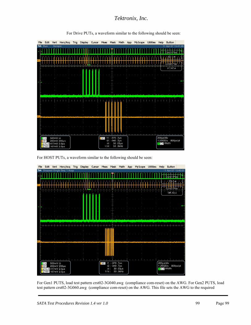
Tektronix, Inc.
For Drive PUTs, a waveform similar to the following should be seen:
For HOST PUTs, a waveform similar to the following should be seen:
For Gen1 PUTS, load test pattern crst02-3G040.awg (compliance com-reset) on the AWG. For Gen2 PUTS, load test pattern crst02-3G060.awg (compliance com-reset) on the AWG. This file sets the AWG to the required
SATA Test Procedures Revision 1.4 ver 1.0 99 Page 99
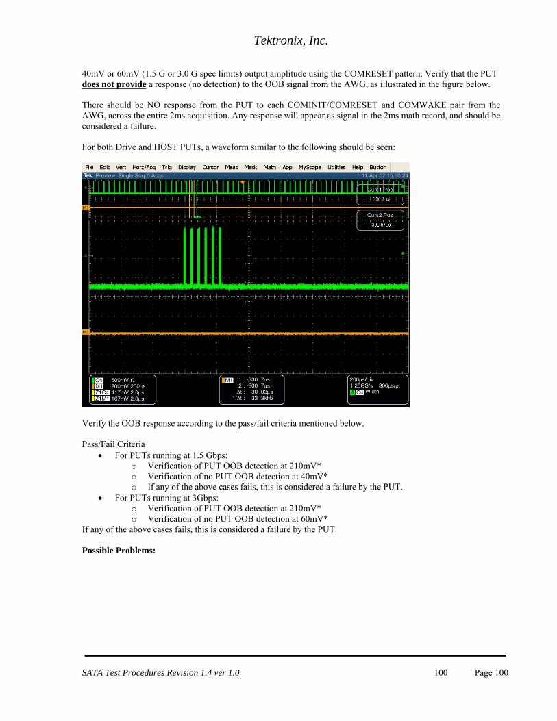
Tektronix, Inc.
40mV or 60mV (1.5 G or 3.0 G spec limits) output amplitude using the COMRESET pattern. Verify that the PUT does not provide a response (no detection) to the OOB signal from the AWG, as illustrated in the figure below.
There should be NO response from the PUT to each COMINIT/COMRESET and COMWAKE pair from the AWG, across the entire 2ms acquisition. Any response will appear as signal in the 2ms math record, and should be considered a failure.
For both Drive and HOST PUTs, a waveform similar to the following should be seen:
Verify the OOB response according to the pass/fail criteria mentioned below.
Pass/Fail Criteria
For PUTs running at 1.5 Gbps: o Verification of PUT OOB detection at 210mV* o Verification of no PUT OOB detection at 40mV* o If any of the above cases fails, this is considered a failure by the PUT.
For PUTs running at 3Gbps: o Verification of PUT OOB detection at 210mV* o Verification of no PUT OOB detection at 60mV*
If any of the above cases fails, this is considered a failure by the PUT. Possible Problems:
SATA Test Procedures Revision 1.4 ver 1.0 100 Page 100
Tektronix, Inc.
Test OOB-02 – UI During OOB Signaling
Test OOB-03 – COMINIT/RESET and COMWAKE Transmit Burst Length
Test OOB-04 – COMINIT/RESET Transmit Gap Length
Test OOB-05 – COMWAKE Transmit Gap Length Purpose: To verify that named parameters during OOB Signaling of the PUT’s transmitter are within the conformance limits. Note. These measurements are combined into a MATLAB post processing analysis tool called SATAOOB. References:
[1] SATA Standard, 7.2.1, Table 32 – OOB Specifications [2] Ibid, 7.2.2.7.2 [3] Ibid, 7.4.11 [4] SATA unified test document, 2.14.2-5
Resource Requirements: See appendix A. SATAOOB.exe is available from:
ftp://ftp.tektronix.com/outgoing/sataoob.zip << Base installer (includes MATLAB) ftp://ftp.tektronix.com/outgoing/sataoob_1_3.zip << UTD 1.3 updated version (install after base)
Note: Version 1.3 of the SATAOOB.exe meets the requirements of ECN #17. Please confirm that you are using version 1.3 of SATAOOB.exe for all SATA program testing. See Appendix C for non TDSRT-Eye setup details. Last Template Modification: May 15, 2006 (Version 1.0) Discussion:
Reference [1] specifies the Transmitted Signal conformance limits for SATA PUTs. This specification includes conformance limits for the UI During OOB Signaling. Reference [2] provides the definition of this term for the purposes of SATA testing. Reference [3] defines the measurement requirements for this test. Test Setup:
Observe the setup outlined in Appendix C. Connect CH1 Analog outputs to PUT receiver inputs. Connect CH1 MKR1 to scope CH4. Connect scope CH1 and CH3 to the PUT Tx+ and Tx- respectively. Load test pattern crst01-3G.AWG (compliance com-reset) on the AWG.
Test Procedure: The following procedure is run once at the maximum interface rate for the PUT (1.5 Gbps or 3Gbps).
1) Recall scope setup file “SATA OOB Timing Setup Normal.set”. 2) Ensure proper test setup and AWG connections (Test Connection) 3) The setup creates MATH1 as CH1-CH3. 4) Acquire one waveform using Single Acq.
SATA Test Procedures Revision 1.4 ver 1.0 101 Page 101
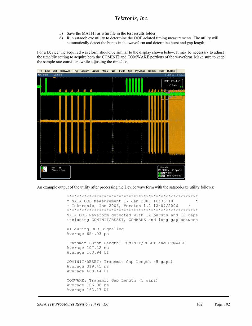
Tektronix, Inc.
5) Save the MATH1 as wfm file in the test results folder 6) Run sataoob.exe utility to determine the OOB-related timing measurements. The utility will
automatically detect the bursts in the waveform and determine burst and gap length. For a Device, the acquired waveform should be similar to the display shown below. It may be necessary to adjust the time/div setting to acquire both the COMINIT and COMWAKE portions of the waveform. Make sure to keep the sample rate consistent while adjusting the time/div.
An example output of the utility after processing the Device waveform with the sataoob.exe utility follows:
***************************************************** * SATA OOB Measurement 17-Jan-2007 16:33:10 * * Tektronix, Inc 2006, Version 1.2 12/07/2006 * ***************************************************** SATA OOB waveform detected with 12 bursts and 12 gaps including COMINIT/RESET, COMWAKE and long gap between UI during OOB Signaling Average 654.03 ps Transmit Burst Length: COMINIT/RESET and COMWAKE Average 107.22 ns Average 163.94 UI COMINIT/RESET: Transmit Gap Length (5 gaps) Average 319.45 ns Average 488.44 UI COMWAKE: Transmit Gap Length (5 gaps) Average 106.06 ns Average 162.17 UI
SATA Test Procedures Revision 1.4 ver 1.0 102 Page 102
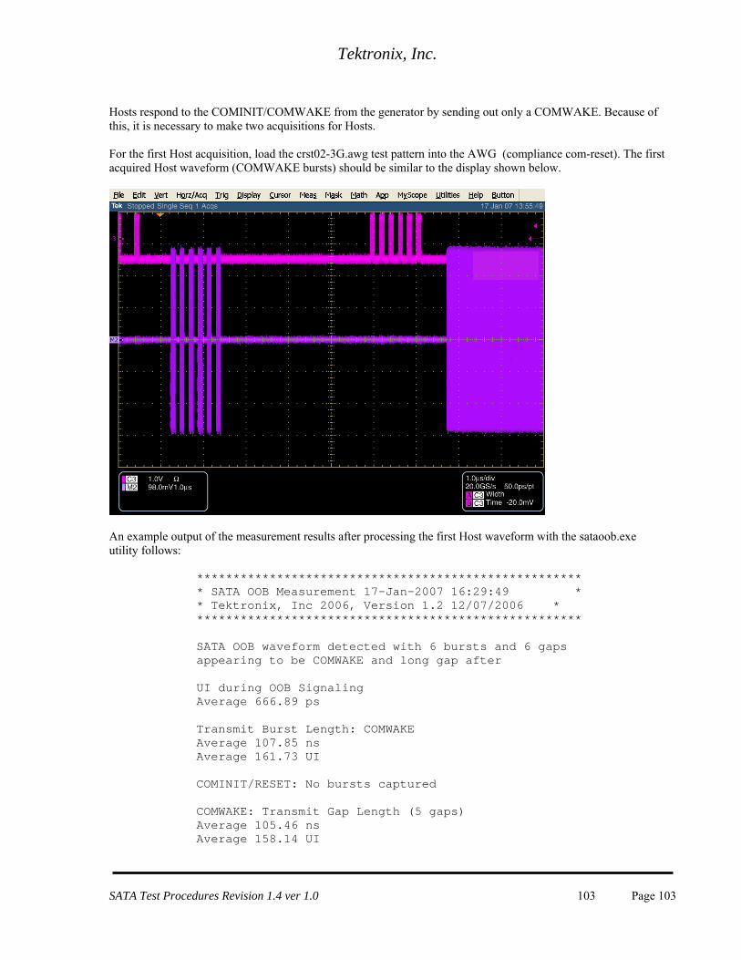
Tektronix, Inc.
Hosts respond to the COMINIT/COMWAKE from the generator by sending out only a COMWAKE. Because of this, it is necessary to make two acquisitions for Hosts. For the first Host acquisition, load the crst02-3G.awg test pattern into the AWG (compliance com-reset). The first acquired Host waveform (COMWAKE bursts) should be similar to the display shown below.
An example output of the measurement results after processing the first Host waveform with the sataoob.exe utility follows:
***************************************************** * SATA OOB Measurement 17-Jan-2007 16:29:49 * * Tektronix, Inc 2006, Version 1.2 12/07/2006 * ***************************************************** SATA OOB waveform detected with 6 bursts and 6 gaps appearing to be COMWAKE and long gap after UI during OOB Signaling Average 666.89 ps Transmit Burst Length: COMWAKE Average 107.85 ns Average 161.73 UI COMINIT/RESET: No bursts captured COMWAKE: Transmit Gap Length (5 gaps) Average 105.46 ns Average 158.14 UI
SATA Test Procedures Revision 1.4 ver 1.0 103 Page 103
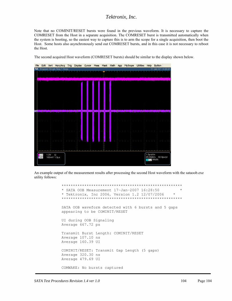
Tektronix, Inc.
Note that no COMINIT/RESET bursts were found in the previous waveform. It is necessary to capture the COMRESET from the Host in a separate acquisition. The COMRESET burst is transmitted automatically when the system is booting, so the easiest way to capture this is to arm the scope for a single acquisition, then boot the Host. Some hosts also asynchronously send out COMRESET bursts, and in this case it is not necessary to reboot the Host. The second acquired Host waveform (COMRESET bursts) should be similar to the display shown below.
An example output of the measurement results after processing the second Host waveform with the sataoob.exe utility follows:
***************************************************** * SATA OOB Measurement 17-Jan-2007 16:28:50 * * Tektronix, Inc 2006, Version 1.2 12/07/2006 * ***************************************************** SATA OOB waveform detected with 6 bursts and 5 gaps appearing to be COMINIT/RESET UI during OOB Signaling Average 667.72 ps Transmit Burst Length: COMINIT/RESET Average 107.10 ns Average 160.39 UI COMINIT/RESET: Transmit Gap Length (5 gaps) Average 320.30 ns Average 479.69 UI COMWAKE: No bursts captured
SATA Test Procedures Revision 1.4 ver 1.0 104 Page 104
Tektronix, Inc.
The final step in processing Host OOB measurements is to average the UI measurements for the COMWAKE and COMRESET acquisitions, and to average the Transmit Burst Length measurements for the COMWAKE and COMRESET acquisitions. Observable Results:
Test OOB-02: The UI During OOB Signaling value shall be between 646.67 and 686.67ps. Test OOB-03: COMINIT/RESET and COMWAKE Transmit Burst shall be between 103.5ns and
109.9ns. Test OOB-04: COMINIT/RESET Transmit Gap shall be between 310.4ns and 329.6ns. Test OOB-05: COMWAKE Transmit Gap Length shall be between 103.5ns and 109.9ns. If measurements are within specified range, they have passed. Otherwise, they have failed.
Possible Problems: Differential or pseudo-differential signals (e.g. MATH1=CH1-CH3) are recommend for this test to avoid
noise problems. If the signal is noisy, or has a lot of crosstalk from adjacent traffic, the utility may have difficulty detecting the idle sections properly.
Some devices have a larger gap between the COMINIT and COMWAKE bursts. It is necessary to make
sure that the acquired waveform contains both the COMINIT/RESET and COMWAKE bursts. Otherwise, the utility will not be able to make the measurements. Make sure that the waveform is captured properly. Another scope setup file is available for working with devices with larger gaps. The file is called “SATA OOB Timing Setup Long.set”. Otherwise, it may be necessary to manually increase the time/div setting on the scope to properly acquire the entire OOB sequence.
SATA Test Procedures Revision 1.4 ver 1.0 105 Page 105
Tektronix, Inc.
Test OOB-06 – COMWAKE Gap Detection Windows Purpose: To verify that the COMWAKE Gap Detection Windows of the PUT’s receiver are within the conformance limits. References:
[1] SATA Standard, 7.2.1, Table 32 – OOB Specifications [2] Ibid, 7.2.2.7.6 [3] Ibid, 7.4.21 [4] SATA unified test document, 2.14.6
Resource Requirements: See appendix A,C Last Template Modification: May 15, 2006 (Version 1.0) Discussion:
Reference [1] specifies the Transmitted Signal conformance limits for SATA PUTs. This specification includes conformance limits for the COMWAKE Gap Detection Windows. Reference [2] provides the definition of this term for the purposes of SATA testing. Reference [3] defines the measurement requirements for this test. Test Setup:
Observe the setup outlined in Appendix C. Connect CH1 Analog outputs to PUT receiver inputs. Connect AWG CH1 MKR1 to scope CH4.
Connect scope CH1 and CH3 to the PUT Tx+ and Tx- respectively. Set scope horizontal settings to 200us/div, 1.25GS/s, and 800ps/pt, Set math (Ch1-Ch3) to 200mV/div. The “SATA oob” settings file can be recalled to quickly put the scope into the desired state.
Test Procedure: This test is run once at the maximum interface rate of the PUT (1.5 Gbps or 3Gbps).
Load the cwke02-3G.awg file into the AWG7102. All of the AWG settings will be made automatically once the file is loaded. This will verify the OOB operation with 110nS comwake burst gap. At this setting, the PUT should respond normally to the OOB sequence. There should be a response from the PUT to every COMWAKE, across the entire 2ms acquisition. Any missing COMWAKEs will appear as gaps in the 2ms record, and should be considered a failure. For Drive PUTs, a waveform similar to the following should be seen:
SATA Test Procedures Revision 1.4 ver 1.0 106 Page 106
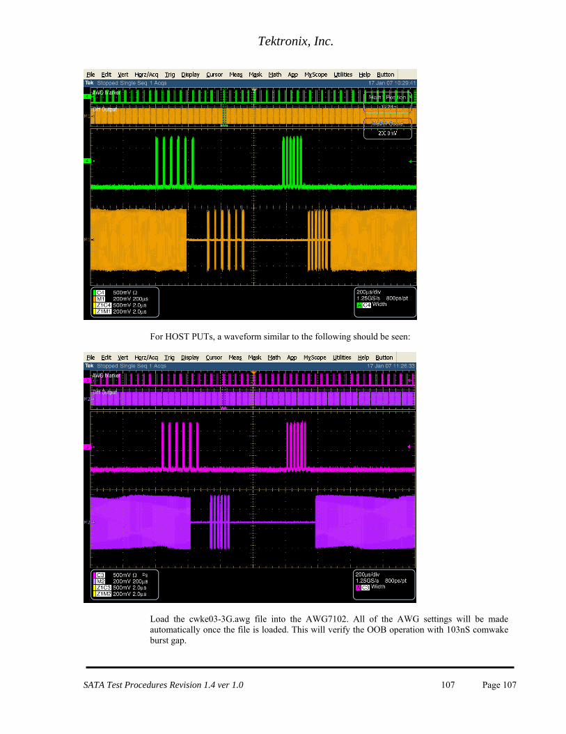
Tektronix, Inc.
For HOST PUTs, a waveform similar to the following should be seen:
Load the cwke03-3G.awg file into the AWG7102. All of the AWG settings will be made automatically once the file is loaded. This will verify the OOB operation with 103nS comwake burst gap.
SATA Test Procedures Revision 1.4 ver 1.0 107 Page 107
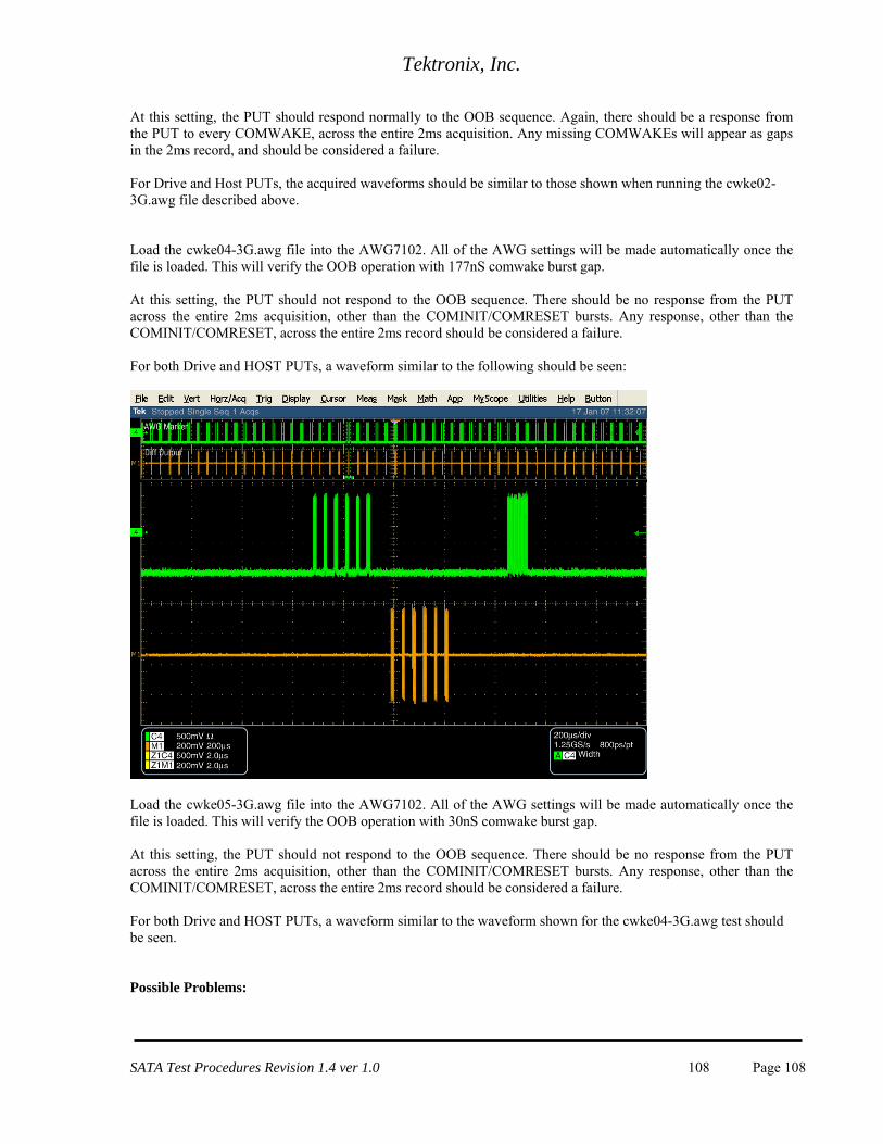
Tektronix, Inc.
At this setting, the PUT should respond normally to the OOB sequence. Again, there should be a response from the PUT to every COMWAKE, across the entire 2ms acquisition. Any missing COMWAKEs will appear as gaps in the 2ms record, and should be considered a failure. For Drive and Host PUTs, the acquired waveforms should be similar to those shown when running the cwke02-3G.awg file described above. Load the cwke04-3G.awg file into the AWG7102. All of the AWG settings will be made automatically once the file is loaded. This will verify the OOB operation with 177nS comwake burst gap. At this setting, the PUT should not respond to the OOB sequence. There should be no response from the PUT across the entire 2ms acquisition, other than the COMINIT/COMRESET bursts. Any response, other than the COMINIT/COMRESET, across the entire 2ms record should be considered a failure. For both Drive and HOST PUTs, a waveform similar to the following should be seen:
Load the cwke05-3G.awg file into the AWG7102. All of the AWG settings will be made automatically once the file is loaded. This will verify the OOB operation with 30nS comwake burst gap. At this setting, the PUT should not respond to the OOB sequence. There should be no response from the PUT across the entire 2ms acquisition, other than the COMINIT/COMRESET bursts. Any response, other than the COMINIT/COMRESET, across the entire 2ms record should be considered a failure. For both Drive and HOST PUTs, a waveform similar to the waveform shown for the cwke04-3G.awg test should be seen.
Possible Problems:
SATA Test Procedures Revision 1.4 ver 1.0 108 Page 108
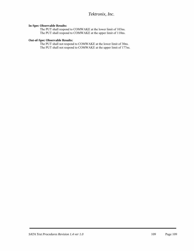
Tektronix, Inc.
In-Spec Observable Results: The PUT shall respond to COMWAKE at the lower limit of 103ns. The PUT shall respond to COMWAKE at the upper limit of 110ns.
Out-of-Spec Observable Results: The PUT shall not respond to COMWAKE at the lower limit of 30ns. The PUT shall not respond to COMWAKE at the upper limit of 177ns.
SATA Test Procedures Revision 1.4 ver 1.0 109 Page 109
Tektronix, Inc.
Test OOB-07 – COMINIT Gap Detection Windows Purpose: To verify that the COMINIT Gap Detection Windows of the PUT’s receiver are within the conformance limits. References:
[1] SATA Standard, 7.2.1, Table 32 – OOB Specifications [2] Ibid, 7.2.2.7.7 [3] Ibid, 7.4.21 [4] SATA unified test document, 2.14.7
Resource Requirements: See appendix A, C Last Template Modification: April 12, 2006 (Version 1.0) Discussion:
Reference [1] specifies the Transmitted Signal conformance limits for SATA PUTs. This specification includes conformance limits for the COMINIT Gap Detection Windows. Reference [2] provides the definition of this term for the purposes of SATA testing. Reference [3] defines the measurement requirements for this test. Test Setup:
Observe the setup outlined in Appendix C. Connect CH1 Analog outputs to PUT receiver inputs. Connect CH1 MKR1 to scope CH4.
Connect scope CH1 and CH3 to the PUT Tx+ and Tx- respectively.
Test Procedure: This test is run once at the maximum interface rate of the PUT (1.5 Gbps or 3Gbps).
Load the crst02-3G.awg file into the AWG7102. All of the AWG settings will be made automatically once the file is loaded. This will verify the OOB operation with 334nS COMRESET/COMINIT burst gap. At this setting, the PUT should respond normally to the OOB sequence. For both Drive and Host PUTs, a waveform similar to the following should be seen:
SATA Test Procedures Revision 1.4 ver 1.0 110 Page 110
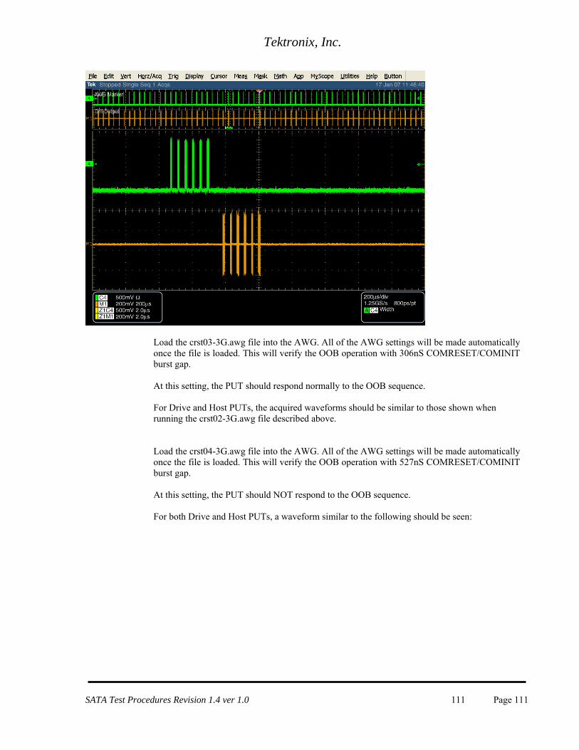
Tektronix, Inc.
Load the crst03-3G.awg file into the AWG. All of the AWG settings will be made automatically once the file is loaded. This will verify the OOB operation with 306nS COMRESET/COMINIT burst gap. At this setting, the PUT should respond normally to the OOB sequence. For Drive and Host PUTs, the acquired waveforms should be similar to those shown when running the crst02-3G.awg file described above.
Load the crst04-3G.awg file into the AWG. All of the AWG settings will be made automatically once the file is loaded. This will verify the OOB operation with 527nS COMRESET/COMINIT burst gap. At this setting, the PUT should NOT respond to the OOB sequence. For both Drive and Host PUTs, a waveform similar to the following should be seen:
SATA Test Procedures Revision 1.4 ver 1.0 111 Page 111

Tektronix, Inc.
Load the crst05-3G.awg file into the AWG. All of the AWG settings will be made automatically once the file is loaded. This will verify the OOB operation with 173nS COMRESET/COMINIT burst gap. At this setting, the PUT should not respond to the OOB sequence. For Drive and Host PUTs, the acquired waveforms should be similar to those shown when running the crst04-3G.awg file described above.
SATA Test Procedures Revision 1.4 ver 1.0 112 Page 112
Tektronix, Inc.
Inter Burst Observable Results:
The PUT shall respond with COMINIT at the lower limit of 306ns. The PUT shall respond with COMINIT at the upper limit of 334ns.
Out-of-Spec Observable Results: The PUT shall not respond with COMINIT at the lower limit of 173ns. The PUT shall not respond with COMINIT at the upper limit of 527ns.
Possible Problems:
The effective detection of out-of-spec behavior can be problematic, particularly when measured on an Oscilloscope. The Instrument is set to single sequence (1 shot trigger) on the first incidence of any traffic from the PUT. Observations have been made which show the PUT responding to the FIRST COMRESET issued by the AWG regardless of its burst properties. The subsequent pulses show no response from the PUT however, which is the spec compliant behavior.
A PUT my take up to 10ms to respond to the received COMRESET. It is necessary to make sure that the
PUT is responding/not responding (as expected) by viewing up to 11ms after the COMRESET. It may be necessary to manually adjust the scope for a larger time/div setting to inspect this 10ms window.
Note: If the PUT supports Asynchronous Signal Recovery, it can pro-actively transmit a COMINIT
which is not in direct response to receiving a COMRESET. During testing, it is essential to ignore any COMINIT which is a result of Asynchronous Signal Recovery, and only test COMINIT responses that are a result of receiving a COMRESET from the AWG.
SATA Test Procedures Revision 1.4 ver 1.0 113 Page 113
Tektronix, Inc.
Appendix A – Resource Requirements
The resource requirements include two separate sets of equipment. The equipment required for PHY and TSG tests is shown in section A.1, and the equipment required for TX and RX tests is shown in section A.2, and the equipment required for OOB tests is shown in section A.3. A.1 Equipment for PHY and TSG tests
1. Real-time Digital Oscilloscope Gen1 Testing: DPO/DSA70804/B or TDS6804B Gen2 Testing: DPO/DSA72004/B, DPO/DSA71604/B, DPO/DSA71254/B, TDS6154C,
TDS6124C Gen3 Testing: DPO/DSA72004/B, DPO/DSA71604/B
2. Test Fixture Crescent Heart Software Fixture TF-SATA-NE/XP, TF-SATA-FE/XP Or equivalent
3. Cables 174-4944-00 or equivalent
4. PRE-TEST system Any system capable of placing the PUT in BIST mode, and producing the desired test pattern.
5. Software PRE-TEST utility as required On TDS Series models: Tektronix TDSJIT3v2 (version 3.0.1 or later), Tektronix TDSRT-
Eye (RTeye version 3.0.2 or later, SST module version 3.0.2 build 9 or later) On DPO and DSA Series models: Tektronix DPOJET (version 2.1.1 or later) or
TDSJIT3v2 (version 3.0.1 or later), Tektronix TDSRT-Eye (RTeye version 3.0.2 or later, SST module version 3.0.2 build 9 or later)
A.2 Equipment for OOB tests
1. Real-time Digital Oscilloscope For Gen3-only testing, the following models are recommended:
DPO/DSA72004/B, DPO/DSA71604/B
For Gen3-only testing, the following models are also acceptable: DPO/DSA71254/B, TDS6154C, TDS612C (These are not acceptable for Gen3 tests)
For Gen1-only testing, the following scopes are also acceptable: DPO/DSA70804/B or TDS6804B (These are not acceptable for Gen3 nor Gen2 tests)
2. Signal Generator
AWG7102, AWG710B, or AWG710 Test Fixture Crescent Heart Software Fixture TF-SATA-NE/XP, TF-SATA-FE/XP Or equivalent
3. Cables 174-4944-00 or equivalent
4. SATA PRE-TEST System
SATA Test Procedures Revision 1.4 ver 1.0 114 Page 114
Tektronix, Inc.
Any system capable of placing the PUT in BIST mode, and producing the desired test pattern.
5. Software PRE-TEST utility as required AWG pattern/sequence files Tektronix DPOJET Jitter and Eye Analysis (version 2.1.1 or later) TDSJIT3v2 (version 3.0.1 or later. Refer to Tektronix SATA MOI for UTD 1.3) Tektronix TDSRT-Eye (RTeye version 3.0.2 or later, SST module version 3.0.2 build 9 or later) SATA OOB Utility (version 1.2 or later)
SATA Test Procedures Revision 1.4 ver 1.0 115 Page 115
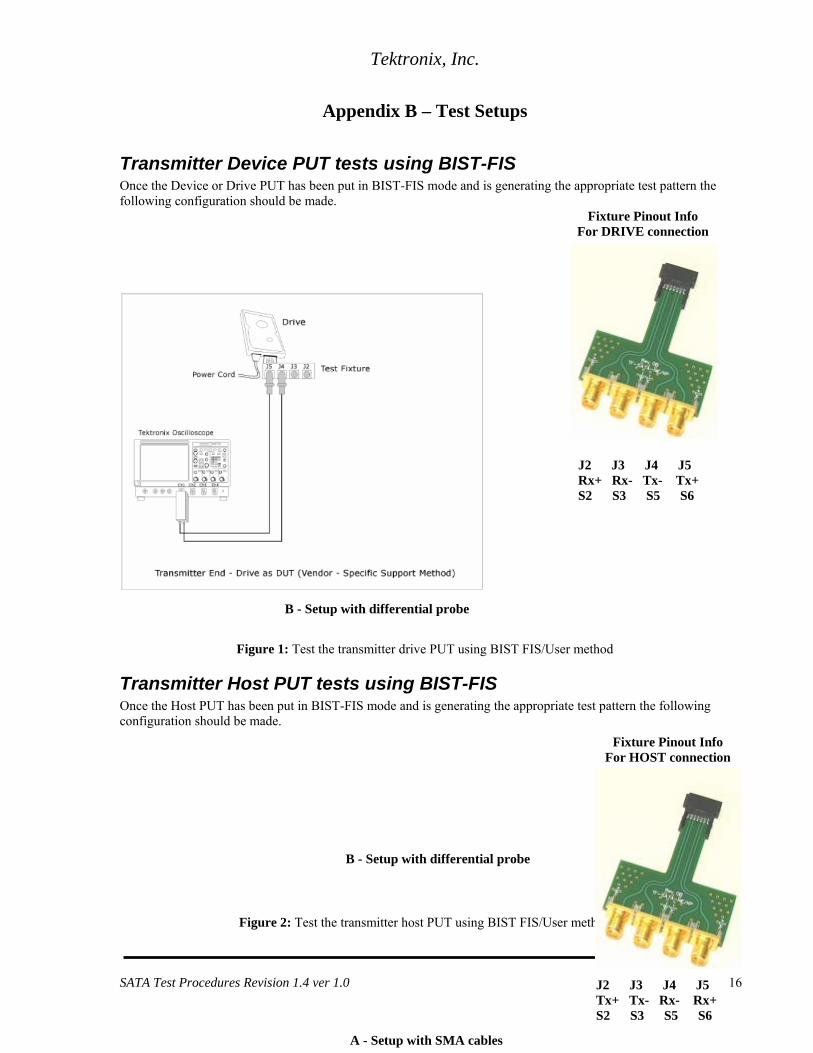
Tektronix, Inc.
Appendix B – Test Setups
Transmitter Device PUT tests using BIST-FIS Once the Device or Drive PUT has been put in BIST-FIS mode and is generating the appropriate test pattern the following configuration should be made.
Fixture Pinout Info For DRIVE connection
A - Setup with SMA cables
J2 J3 J4 J5 Rx+ Rx- Tx- Tx+S2 S3 S5 S6
B - Setup with differential probe
Figure 1: Test the transmitter drive PUT using BIST FIS/User method
Transmitter Host PUT tests using BIST-FIS Once the Host PUT has been put in BIST-FIS mode and is generating the appropriate test pattern the following configuration should be made.
Figure 2: Test the transmitter host PUT using BIST FIS/User method
A - Setup with SMA cables
B - Setup with differential probe
SATA Test Procedures Revision 1.4 ver 1.0 116 Page 116
Fixture Pinout Info For HOST connection
J2 J3 J4 J5 Tx+ Tx- Rx- Rx+S2 S3 S5 S6
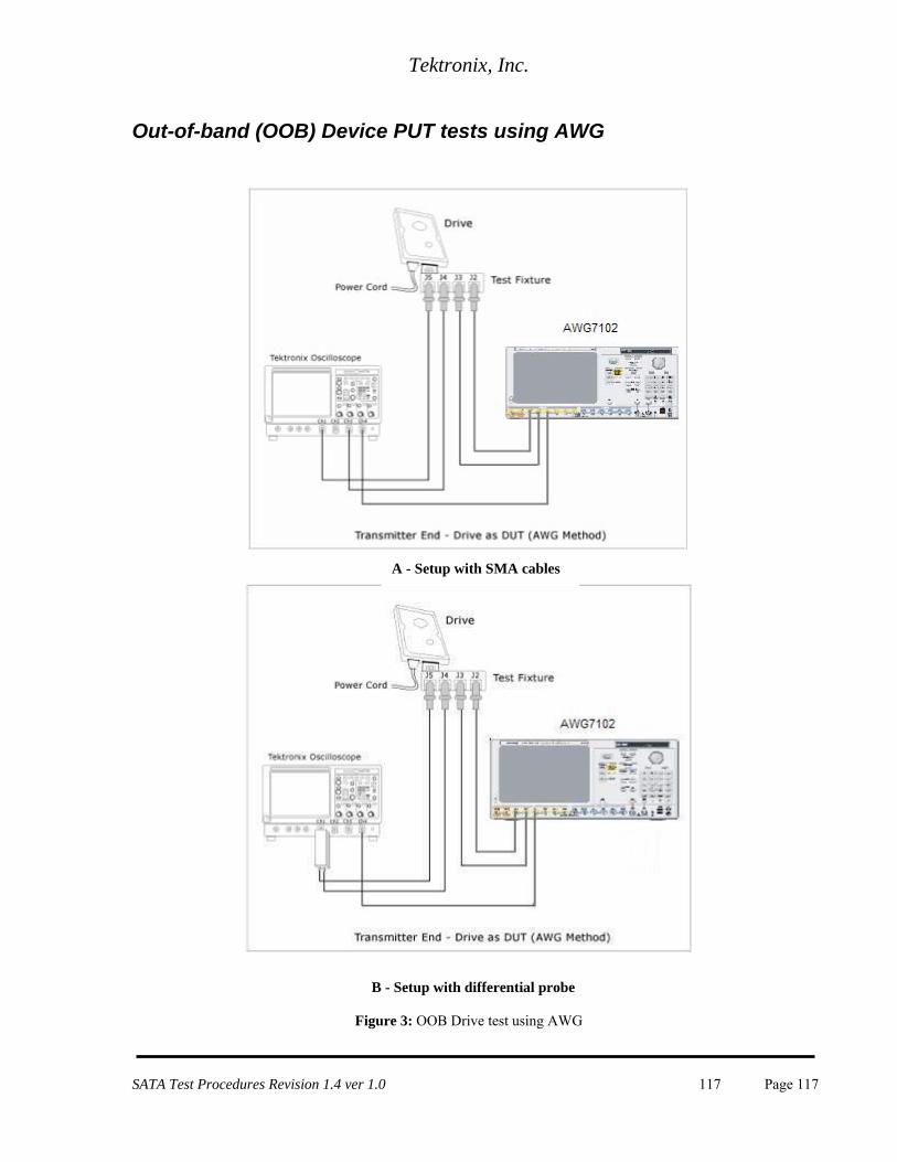
Tektronix, Inc.
Out-of-band (OOB) Device PUT tests using AWG
A - Setup with SMA cables
B - Setup with differential probe
Figure 3: OOB Drive test using AWG
SATA Test Procedures Revision 1.4 ver 1.0 117 Page 117
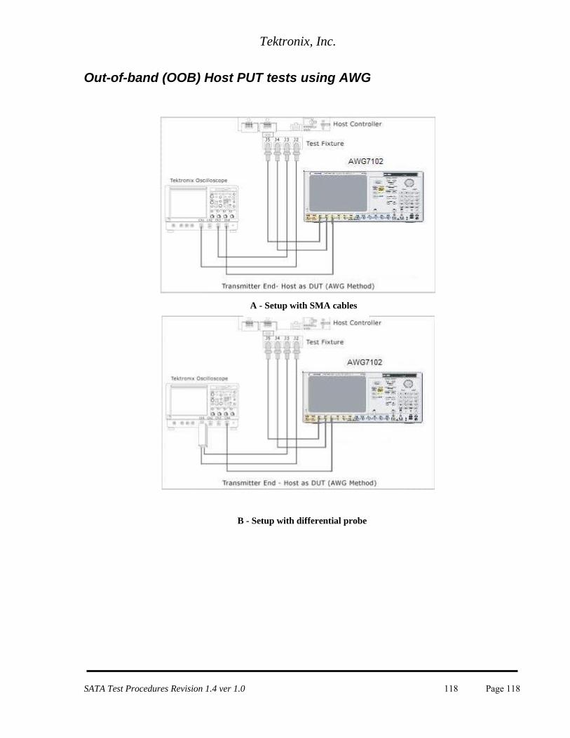
Tektronix, Inc.
Out-of-band (OOB) Host PUT tests using AWG
A - Setup with SMA cables
B - Setup with differential probe
SATA Test Procedures Revision 1.4 ver 1.0 118 Page 118
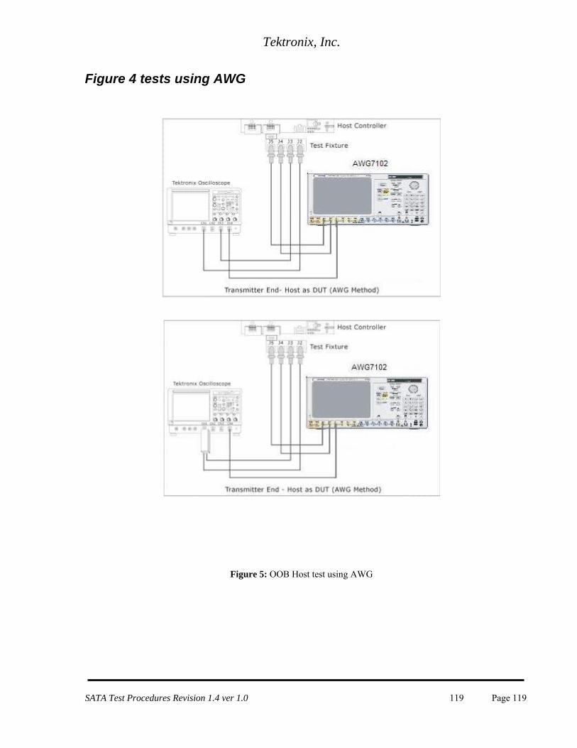
Tektronix, Inc.
Figure 4 tests using AWG
Figure 5: OOB Host test using AWG
SATA Test Procedures Revision 1.4 ver 1.0 119 Page 119
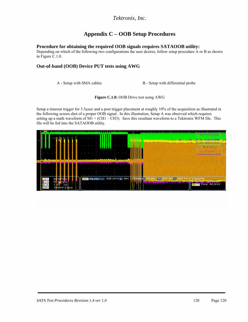
Tektronix, Inc.
Appendix C – OOB Setup Procedures
Procedure for obtaining the required OOB signals requires SATAOOB utility: Depending on which of the following two configurations the user desires, follow setup procedure A or B as shown in Figure C.1.0. Out-of-band (OOB) Device PUT tests using AWG
A - Setup with SMA cables B - Setup with differential probe
Figure C.1.0: OOB Drive test using AWG
Setup a timeout trigger for 3.5µsec and a post trigger placement at roughly 10% of the acquisition as illustrated in the following screen shot of a proper OOB signal. In this illustration, Setup A was observed which requires setting up a math waveform of M1 = (CH1 – CH3). Save this resultant waveform to a Tektronix WFM file. This file will be fed into the SATAOOB utility.
SATA Test Procedures Revision 1.4 ver 1.0 120 Page 120
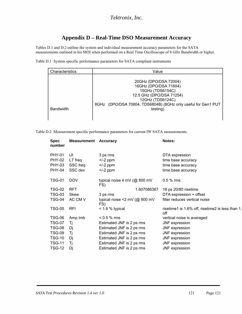
Tektronix, Inc.
Appendix D – Real-Time DSO Measurement Accuracy Tables D.1 and D.2 outline the system and individual measurement accuracy parameters for the SATA measurements outlined in his MOI when performed on a Real Time Oscilloscope of 8 GHz Bandwidth or higher. Table D.1 System specific performance parameters for SATA compliant instruments
Characteristics Value
Bandwidth
20GHz (DPO/DSA 72004) 16GHz (DPO/DSA 71604)
15GHz (TDS6154C) 12.5 GHz (DPO/DSA 71254)
12GHz (TDS6124C) 8GHz (DPO/DSA 70804, TDS6804B) (8GHz only useful for Gen1 PUT
testing)
Table D.2 Measurement specific performance parameters for current IW SATA measurements.
Spec number
Measurement Accuracy Notes:
PHY-01 UI 3 ps rms DTA expression PHY-02 LT freq +/-2 ppm time base accuracy PHY-03 SSC freq +/-2 ppm time base accuracy PHY-04 SSC dev +/-2 ppm time base accuracy TSG-01 DOV typical noise 4 mV (@ 800 mV
FS) 0.5 % rms
TSG-02 RFT 1.607086367 18 ps 20/80 risetime TSG-03 Skew 3 ps rms DTA expression + offset TSG-04 AC CM V typical noise <2 mV (@ 800 mV
FS) filter reduces vertical noise
TSG-05 RFI < 1.6 % typical risetime1 is 1.6% off, risetime2 is less than 1.6off
TSG-06 Amp Imb < 0.5 % rms vertical noise is averaged TSG-07 Tj Estimated JNF is 2 ps rms JNF expression TSG-08 Dj Estimated JNF is 2 ps rms JNF expression TSG-09 Tj Estimated JNF is 2 ps rms JNF expression TSG-10 Dj Estimated JNF is 2 ps rms JNF expression TSG-11 Tj Estimated JNF is 2 ps rms JNF expression TSG-12 Dj Estimated JNF is 2 ps rms JNF expression
SATA Test Procedures Revision 1.4 ver 1.0 121 Page 121
Tektronix, Inc.
Appendix E – Return Loss Verification Procedure This procedure outlines the use of a Time Domain Network Analyzer (TDNA) to measure/verify the Lab Load return loss. Since there is good correlation between return loss measurements made a TDNA and a Vector Network Analyzer (VNA), it is acceptable to make the measurement with either system. The SATA specification requires that the Lab Load (scope input, including cables) have a return loss of -20dB or more up to 5GHz, and -10dB or more from 5GHz to 8GHz. The Tek scopes meet this requirement at all settings, except for the 50mV/div setting. At the 50mV/div setting, the use of an external 6dB attenuator allows meeting the specification, without significantly impacting the quality or integrity of the measurement. Empirical data has shown that the return loss performance does not substantially impact the measurement results; reliable measurements can be made for debug and diagnostic work without using external attenuators. However, it is necessary to add the external attenuation during the SATA Compliance Tests to assure meeting the SATA specification requirements for Lab Loads. The return loss performance of the Lab Load (TDS scope) is stable over time. Perform this procedure once for each of the channels being used on the scope prior to an Interoperability Workshop/Compliance Test session to verify that the Lab Load meets the SATA specification requirements. The Tek TDNA systems consists of the following equipment:
TDS8000, TDS8200, or CSA8200 equivalent time sampling scope 80E04 sampling module Tek Iconnect TDNA software
To calibrate the measurements, a high quality 50 ohm SMA cable, and high quality 50 ohm calibration load is needed. Detailed Procedure: Turn on the power of the scope, and set the vertical sensitivity to 50mV/div for the channel being tested. All other settings for the scope do not effect the return loss. Install a TCA-SMA adapter, and connect a 6dB SMA attenuator to the TCA-SMA. Connect the SMA cable (the same cable that will be used for PUT testing) to the 6dB attenuator. On the TDNA system, make the following settings: Vert: 100mV/div Position = 1 div Offset = 250mV Horiz: 2ns/div Record length = 4000 Position approx. 35ns ACQ: Average 128 samples Set “Stop After” to Condition = Average Complete Acquire Open Reference Trace Using the TDNA scope setup controls, turn on TDR and ACQ (under the TDR setup tab). It is necessary to adjust the horizontal position on the TDNA scope to move the incident pulse just off the left side of the display. When using the SMA connector on the 80E04 as the reference plane, it can be difficult to make this adjustment. By connecting a short, high quality SMA cable to the front of the 80E04, the reference plane can be
SATA Test Procedures Revision 1.4 ver 1.0 122 Page 122
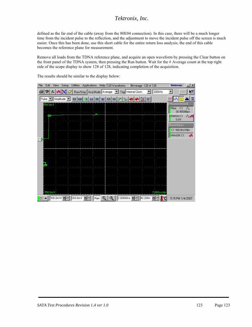
Tektronix, Inc.
defined as the far end of the cable (away from the 80E04 connection). In this case, there will be a much longer time from the incident pulse to the reflection, and the adjustment to move the incident pulse off the screen is much easier. Once this has been done, use this short cable for the entire return loss analysis; the end of this cable becomes the reference plane for measurement. Remove all loads from the TDNA reference plane, and acquire an open waveform by pressing the Clear button on the front panel of the TDNA system, then pressing the Run button. Wait for the # Average count at the top right side of the scope display to show 128 of 128, indicating completion of the acquisition. The results should be similar to the display below:
SATA Test Procedures Revision 1.4 ver 1.0 123 Page 123
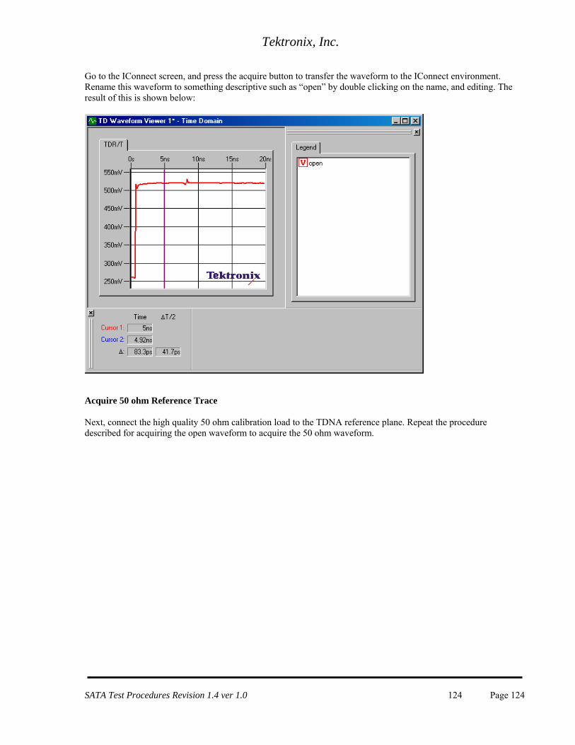
Tektronix, Inc.
Go to the IConnect screen, and press the acquire button to transfer the waveform to the IConnect environment. Rename this waveform to something descriptive such as “open” by double clicking on the name, and editing. The result of this is shown below:
Acquire 50 ohm Reference Trace Next, connect the high quality 50 ohm calibration load to the TDNA reference plane. Repeat the procedure described for acquiring the open waveform to acquire the 50 ohm waveform.
SATA Test Procedures Revision 1.4 ver 1.0 124 Page 124
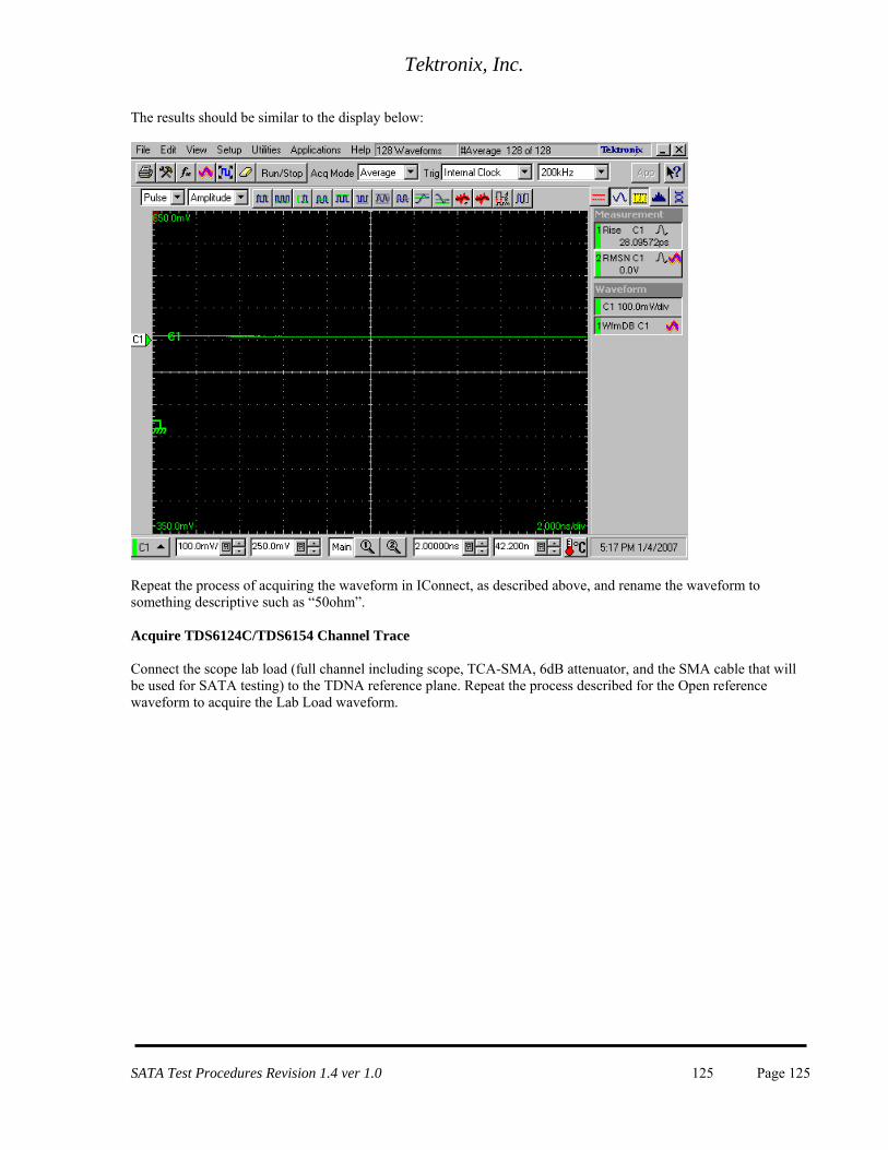
Tektronix, Inc.
The results should be similar to the display below:
Repeat the process of acquiring the waveform in IConnect, as described above, and rename the waveform to something descriptive such as “50ohm”. Acquire TDS6124C/TDS6154 Channel Trace Connect the scope lab load (full channel including scope, TCA-SMA, 6dB attenuator, and the SMA cable that will be used for SATA testing) to the TDNA reference plane. Repeat the process described for the Open reference waveform to acquire the Lab Load waveform.
SATA Test Procedures Revision 1.4 ver 1.0 125 Page 125
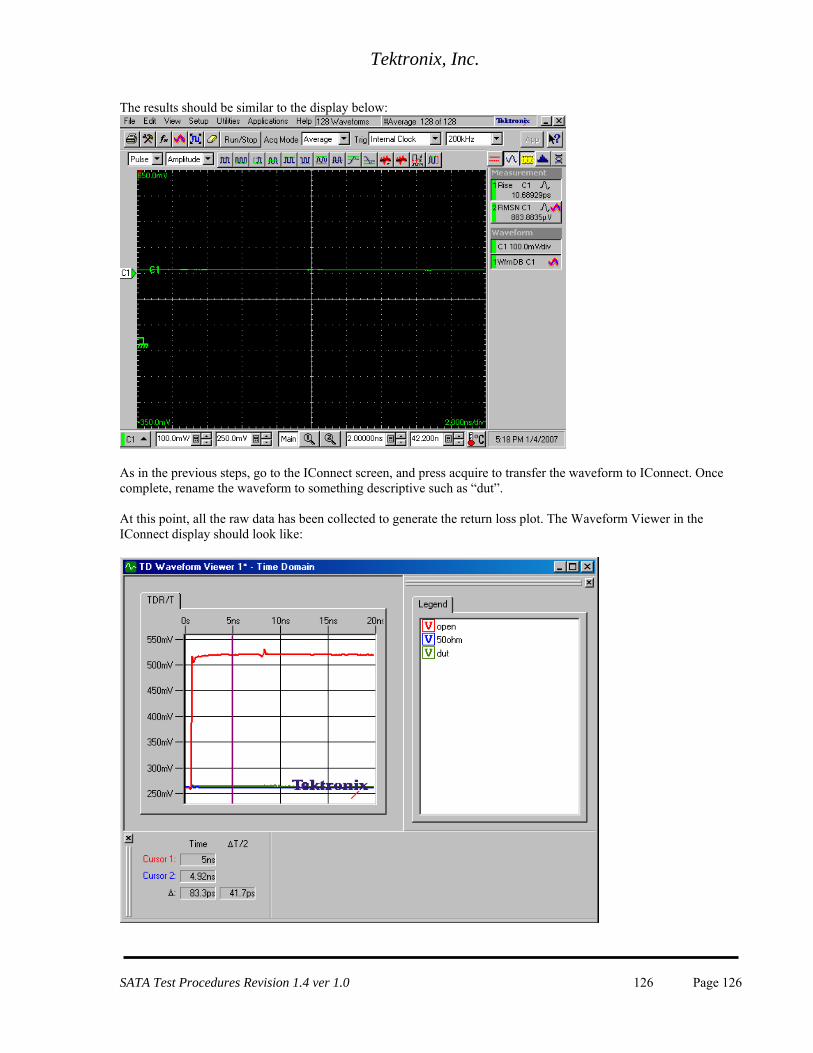
Tektronix, Inc.
The results should be similar to the display below:
As in the previous steps, go to the IConnect screen, and press acquire to transfer the waveform to IConnect. Once complete, rename the waveform to something descriptive such as “dut”. At this point, all the raw data has been collected to generate the return loss plot. The Waveform Viewer in the IConnect display should look like:
SATA Test Procedures Revision 1.4 ver 1.0 126 Page 126
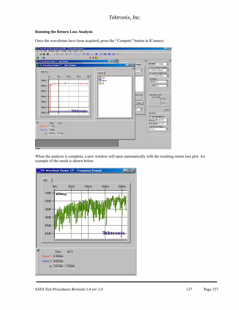
Tektronix, Inc.
Running the Return Loss Analysis Once the waveforms have been acquired, press the “Compute” button in IConnect.
When the analysis is complete, a new window will open automatically with the resulting return loss plot. An example of the result is shown below.
SATA Test Procedures Revision 1.4 ver 1.0 127 Page 127
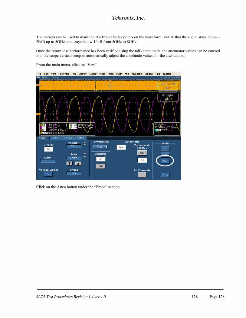
Tektronix, Inc.
The cursors can be used to mark the 5GHz and 8GHz points on the waveform. Verify that the signal stays below -20dB up to 5GHz, and stays below 10dB from 5GHz to 8GHz. Once the return loss performance has been verified using the 6dB attenuators, the attenuator values can be entered into the scope vertical setup to automatically adjust the amplitude values for the attenuation. From the main menu, click on “Vert”.
Click on the Atten button under the “Probe” section.
SATA Test Procedures Revision 1.4 ver 1.0 128 Page 128
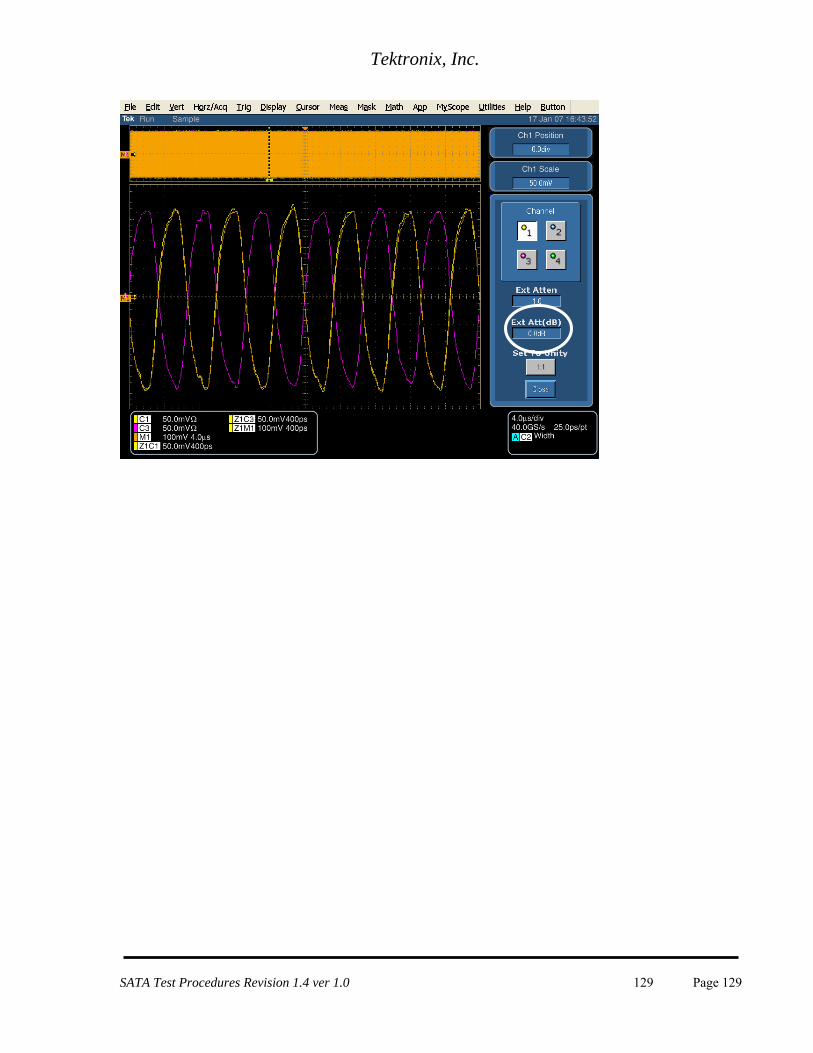
Tektronix, Inc.
SATA Test Procedures Revision 1.4 ver 1.0 129 Page 129
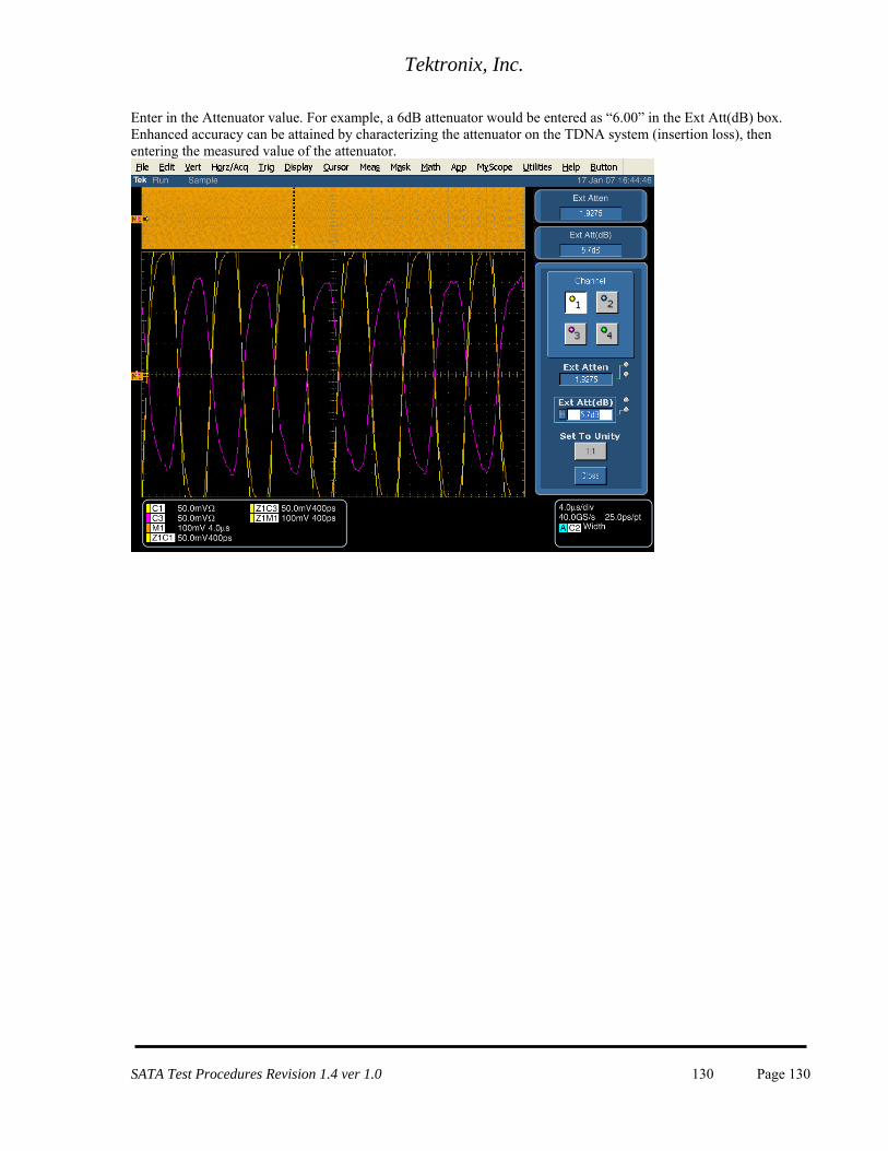
Tektronix, Inc.
Enter in the Attenuator value. For example, a 6dB attenuator would be entered as “6.00” in the Ext Att(dB) box. Enhanced accuracy can be attained by characterizing the attenuator on the TDNA system (insertion loss), then entering the measured value of the attenuator.
SATA Test Procedures Revision 1.4 ver 1.0 130 Page 130
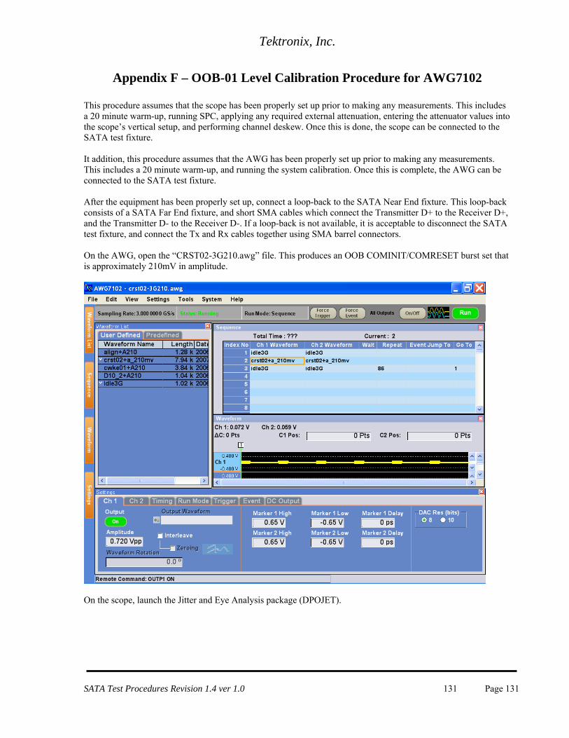
Tektronix, Inc.
Appendix F – OOB-01 Level Calibration Procedure for AWG7102
This procedure assumes that the scope has been properly set up prior to making any measurements. This includes a 20 minute warm-up, running SPC, applying any required external attenuation, entering the attenuator values into the scope’s vertical setup, and performing channel deskew. Once this is done, the scope can be connected to the SATA test fixture. It addition, this procedure assumes that the AWG has been properly set up prior to making any measurements. This includes a 20 minute warm-up, and running the system calibration. Once this is complete, the AWG can be connected to the SATA test fixture. After the equipment has been properly set up, connect a loop-back to the SATA Near End fixture. This loop-back consists of a SATA Far End fixture, and short SMA cables which connect the Transmitter D+ to the Receiver D+, and the Transmitter D- to the Receiver D-. If a loop-back is not available, it is acceptable to disconnect the SATA test fixture, and connect the Tx and Rx cables together using SMA barrel connectors. On the AWG, open the “CRST02-3G210.awg” file. This produces an OOB COMINIT/COMRESET burst set that is approximately 210mV in amplitude.
On the scope, launch the Jitter and Eye Analysis package (DPOJET).
SATA Test Procedures Revision 1.4 ver 1.0 131 Page 131
Tektronix, Inc.
Recall the settings file “SATA OOB 210mv cal”. This will configure the scope as well as the DPOJET settings. Note that the SATA Logo group has defined this measurement to be made using a MODE measurement on the .45 to .55 (center 10%) portion of the UI, and to average the MODE measurements of all of the UI contained in all of the COMINIT bursts. It is not necessary to manually set the DPOJET settings after loading the settings file, but the following screen shows the settings that are created by the “SATA OOB 210mv cal” setup file:
SATA Test Procedures Revision 1.4 ver 1.0 132 Page 132
Tektronix, Inc.
Click on the “Run” button, and while the measurement is running, adjust the AWG output amplitude as close as possible to 210mV. It might be convenient to stop the measurement, clear the previous data, and restart the data to get a more accurate reading. If everything is configured properly, it will be easy to get better than 1% error (+/-2mV) on this adjustment. The following screen shows the adjustment window:
SATA Test Procedures Revision 1.4 ver 1.0 133 Page 133
Tektronix, Inc.
The results will be displayed on the scope in the following location:
SATA Test Procedures Revision 1.4 ver 1.0 134 Page 134
Tektronix, Inc.
Repeat the procedure for the 40mV and 60mV settings. The AWG files used to generate the signals are “CRST02-3G040.awg” and “CRST02-3G060.awg”. The setup files for the scope to make these measurements are “SATA OOB 40mv cal.set” and “SATA OOB 60mv cal.set”.
SATA Test Procedures Revision 1.4 ver 1.0 135 Page 135
Tektronix, Inc.
Appendix G – Calibration and Verification of Jitter Measurement Devices
In an effort to get better correlation between different jitter measurement systems, the SATA PHY group has defined a standard jitter transfer function requirement which all jitter measurement systems must meet. This is detailed in ECN-008. The following procedure describes the process for performing the Jitter Transfer Function calibration. This calibration must be done once prior to making TSG-09 through TSG-16. The response to jitter of the Jitter Measurement Device (JMD)(the reference clock is part of the JMD) is measured with three different jitter modulation frequencies corresponding to the three cases: 1) SSC (full tracking) 2) jitter (no tracking) 3) the boundary between SSC and jitter. The jitter source is independently verified by separate means. This ensures the jitter response of the JMD is reproducible across different test setups. The three Gen1i test signals are: 1) a 375MHz +/- 0.035% square wave (which is a D24.3, 00110011 pattern) with risetime between 67ps and 136ps 20 to 80% [1] with a sinusoidal phase modulation of 20.8ns +/- 10% peak to peak at 30kHz +/- 1%. 2) a 375MHz square wave with a sinusoidal phase modulation of 200ps +/- 10% peak to peak at 50MHz +/- 1%. 3) a 375MHz square wave with no modulation. The three Gen2i test signals are: 1) a 750MHz +/- 0.035% square wave (which is a D24.3, 00110011 pattern) with risetime between 67ps and 136ps 20 to 80% [1] with a sinusoidal phase modulation of 20.8ns +/- 10% peak to peak at 30kHz +/- 1%. 2) a 750MHz square wave with a sinusoidal phase modulation of 100ps +/- 10% peak to peak at 50MHz +/- 1%. 3) a 750MHz square wave with no modulation The three Gen3i test signals are: 1) a 1500MHz +/- 0.035% square wave (which is a D24.3, 00110011 pattern) with risetime between 33ps and 67ps (20 to 80%) [1] with a sinusoidal phase modulation of 1.0ns +/- 10% peak to peak at 420kHz +/- 1%. 2) a 1500MHz square wave with a sinusoidal phase modulation of 50ps +/- 10% peak to peak at 50MHz +/- 1%. 3) a 1500MHz square wave with no modulation. The independent separate means of verification of the test signals is a time interval error plot on a real time oscilloscope. The test procedure checks two conditions: the JTF attenuation and the JTF bandwidth. Care is taken to minimize the number of absolute measurements taken, making most relative; this reduces the dependencies and improves accuracy. The basic procedure is as follows:
1. Adjust the pattern generator for a D24.3 pattern (00110011) with the signal characteristics described for the data rate being tested as described above. For example, Gen2i is a 750MHz sine wave and modulation to produce a 30 KHz +/- 1%, 20.8 ns p-p +/- 10% sinusoidal phase modulation.
2. Verify the level of modulation meets the requirements and record the p-p level (DJ t). This is done with a Time Interval Error (TIE) type measurement or equivalent.
3. Apply test signal to the JMD. Turn on the sinusoidal phase modulation. Record the reported DJ. 4. Turn off the sinusoidal phase modulation. Record the reported residual DJ. 5. Calculate and record the level of applied DJ by subtracting the DJ with modulation off from DJ with
modulation on. 6. Calculate the jitter attenuation by 20Log(DJ m / DJ t). This value must fall within the range of –72dB
+/- 3dB. Adjust the JMD settings to match this requirement. 7. Adjust the pattern generator for a D24.3 pattern (00110011) and modulation to produce a 50 MHz +/-1%,
0.3 UI p-p +/- 10% (200ps for Gen1i or 100ps for Gen2i) sinusoidal phase modulation, also known as periodic jitter, PJ
8. Verify the level of modulation meets the requirements and record the p-p level (DJ t). This is done with a Time Interval Error (TIE) type measurement or equivalent.
9. Apply test signal to the JMD. Record the level as the reference DJ value (DJ 0dB). 10. Calculate the -3dB value: DJ -3dB = DJ 0dB * 10^(-3/20)
SATA Test Procedures Revision 1.4 ver 1.0 136 Page 136
Tektronix, Inc.
11. Adjust the frequency of the DJ source to 2.1MHz. Shift the frequency of the PJ source until the reported DJ difference between PJ on versus PJ off is equal to (DJ -3dB). The PJ frequency is the -3dB BW of the JTF.
12. Adjust the JMD settings to bring the PJ –3dB frequency to 2.1MHz +/- 1MHz. Repeat step 4 through step 12 until both the jitter attenuation and 3dB frequency are in the acceptable ranges.
13. Check the peaking of the JTF. Adjust the pattern generator for a D24.3 pattern and modulation to produce sinusoidal phase modulation at the –3dB frequency and 0.3 UI p-p +/- 10% (200ps for Gen1i or 100ps for Gen2i). Increase the frequency of the modulation to find a maximum jitter; it is not necessary to increase beyond 20MHz. Record the maximum jitter value and frequency.
14. Calculate the JTF Peaking value: 20Log (DJ pkng/ DJ 0dB). Record this value. For general reference, the following Damping and 3dB Corner Frequency values were calculated on a typical recommended oscilloscope configuration for SATA testing: DPO72004B w/DPOJET Version 2.1.1
Gen1: Damping = 700m Corner Frequency (Entered as ‘Loop BW’ in DPOJET) = 1.98 MHz
Gen2: Damping = 700m Corner Frequency (Entered as ‘Loop BW’ in DPOJET) = 1.98 MHz
Gen3: Damping = 600m Corner Frequency (Entered as ‘Loop BW’ in DPOJET) = 4.2 MHz
Detailed Procedure: Equipment list:
AWG7102 with Opt 6 JTF Waveform Library for AWG7102 or suitable AWG7000 model
o SATA Gen1 30k 62_5Sj.awg o SATA Gen2 30k 62_5Sj.awg o SATA Gen3.awg
Test cables DSA72004 Digital Phosphor Oscilloscope 20GHz, 50G/s, or desired BW Option DJA (DPOJET) and oscilloscope set up files
o Gen1: JTF_DJA_Gen1.set o Gen2: JTF_DJA_Gen2.set o Gen3: JTF_DJA_Gen3.set
The oscilloscope should be calibrated and its channels deskewed before performing this test. This example will use waveforms and measurements for SATA Gen2. Appropriate waveform files for the AWG7000 series for all SATA data rates are identified by the ‘Gen#’ portion of the waveform file names. Step 1: Adjust the pattern generator for a D24.3 pattern (00110011)(MFTP) and modulation to produce a 30 KHz +/- 1%, 20.8 ns p-p +/- 10% sinusoidal phase modulation. To do this on the AWG7102, follow steps “a” through “c” below. Open the waveform file SATA Gen2 30k 62_5Sj.awg. This will set all parameters of the AWG.
a) Connect the AWG to the scope, using the same matched cable set that will be connected to the scope during normal jitter measurements. Verify that the cables are connected to the AWG Interleaved outputs.
b) Open the waveform file “SATA Gen2 30k 62_5Sj.awg”. Select the Gen2 30kHz 62_5sj” waveform from
the Waveform List on the left side of the display. Drag this to the Waveform display window, and drop in the CH1 area. When the pop-up appears, choose “Set Waveform”.
SATA Test Procedures Revision 1.4 ver 1.0 137 Page 137
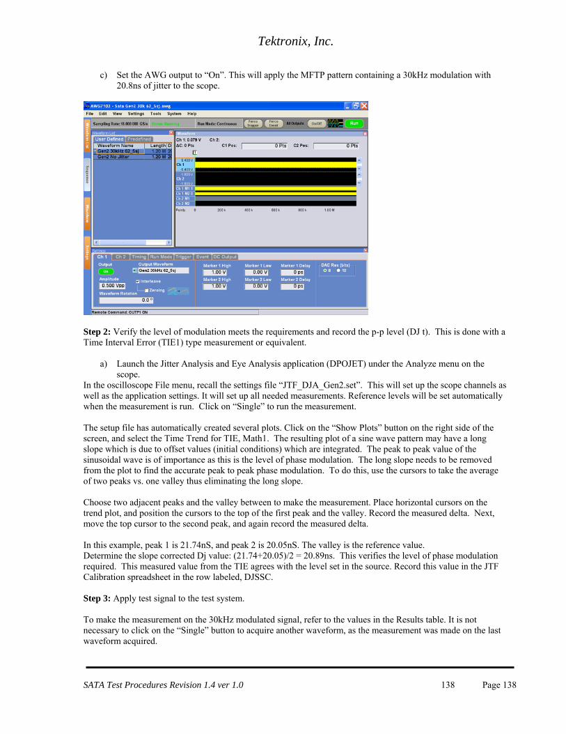
Tektronix, Inc.
c) Set the AWG output to “On”. This will apply the MFTP pattern containing a 30kHz modulation with 20.8ns of jitter to the scope.
Step 2: Verify the level of modulation meets the requirements and record the p-p level (DJ t). This is done with a Time Interval Error (TIE1) type measurement or equivalent.
a) Launch the Jitter Analysis and Eye Analysis application (DPOJET) under the Analyze menu on the scope.
In the oscilloscope File menu, recall the settings file “JTF_DJA_Gen2.set”. This will set up the scope channels as well as the application settings. It will set up all needed measurements. Reference levels will be set automatically when the measurement is run. Click on “Single” to run the measurement. The setup file has automatically created several plots. Click on the “Show Plots” button on the right side of the screen, and select the Time Trend for TIE, Math1. The resulting plot of a sine wave pattern may have a long slope which is due to offset values (initial conditions) which are integrated. The peak to peak value of the sinusoidal wave is of importance as this is the level of phase modulation. The long slope needs to be removed from the plot to find the accurate peak to peak phase modulation. To do this, use the cursors to take the average of two peaks vs. one valley thus eliminating the long slope. Choose two adjacent peaks and the valley between to make the measurement. Place horizontal cursors on the trend plot, and position the cursors to the top of the first peak and the valley. Record the measured delta. Next, move the top cursor to the second peak, and again record the measured delta. In this example, peak 1 is 21.74nS, and peak 2 is 20.05nS. The valley is the reference value. Determine the slope corrected Dj value: (21.74+20.05)/2 = 20.89ns. This verifies the level of phase modulation required. This measured value from the TIE agrees with the level set in the source. Record this value in the JTF Calibration spreadsheet in the row labeled, DJSSC. Step 3: Apply test signal to the test system. To make the measurement on the 30kHz modulated signal, refer to the values in the Results table. It is not necessary to click on the “Single” button to acquire another waveform, as the measurement was made on the last waveform acquired.
SATA Test Procedures Revision 1.4 ver 1.0 138 Page 138
Tektronix, Inc.
Record this measured value of DJ1, Math1 (DJ1) into the JTF Calibration spreadsheet in the row labeled, DJSSCON. Step 4: Next, measure the residual jitter. This is done by turning off the 30kHz modulation, and making another jitter measurement. On the AWG, drag the “Gen2 No Jitter” waveform from the waveform list to the waveform display area, and drop in CH1. When the pop-up window appears, select “Set Waveform”. Turn the AWG Ch1 output on. On the scope, click on “Clear” to remove the prior results and then the “Single” button to make another acquisition. Record the DJ1 measurement into the JTF Calibration spreadsheet in the row labeled, DJSSCOFF as. Step 5: The spreadsheet calculates the level of applied DJ by subtracting the DJ with modulation off from DJ with modulation on. (e.g. 7.30pS - 2.53pS = 4.77pS). Step 6: The spreadsheet calculates the jitter attenuation by 20Log(DJ m / DJ t). In this example it is 20 Log (4.779pS / 20.9nS) = -72.84dB. This value must fall within the range of –72dB +/- 3dB. If the result in Cell I9 is Fail, adjust the JMD Loop Bandwidth setting under the Clock Recovery setup to meet this requirement. If the calculated attenuation is below -72dB, decrease the Loop Bandwidth setting, and repeat the process from step 1 to 6 until the required attenuation is attained. Once the proper Loop Bandwidth has been determined, use this value setting for all subsequent jitter measurements. Step 7: Adjust the pattern generator for a D24.3 pattern (00110011) and modulation to produce a 50 MHz +/-1%, 0.3 UI p-p +/- 10% sinusoidal phase modulation. To do this on the AWG7102, open the waveform file “SATA Gen1 JTF 3db set.awg” or “SATA Gen2 JTF 3db set.awg”. This will set all parameters of the AWG. This setup file includes a collection of waveforms that can be used to verify the -3dB point on the jitter transfer curve.
SATA Test Procedures Revision 1.4 ver 1.0 139 Page 139
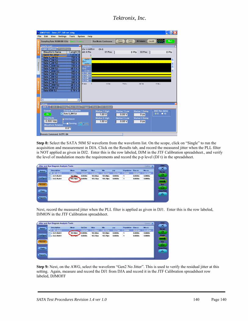
Tektronix, Inc.
Step 8: Select the SATA 50M SJ waveform from the waveform list. On the scope, click on “Single” to run the acquisition and measurement in DJA. Click on the Results tab, and record the measured jitter when the PLL filter is NOT applied as given in DJ2. Enter this is the row labeled, DJM in the JTF Calibration spreadsheet., and verify the level of modulation meets the requirements and record the p-p level (DJ t) in the spreadsheet.
Next, record the measured jitter when the PLL filter is applied as given in DJ1. Enter this is the row labeled, DJMON in the JTF Calibration spreadsheet.
Step 9: Next, on the AWG, select the waveform “Gen2 No Jitter”. This is used to verify the residual jitter at this setting. Again, measure and record the DJ1 from DJA and record it in the JTF Calibration spreadsheet row labeled, DJMOFF
SATA Test Procedures Revision 1.4 ver 1.0 140 Page 140
Tektronix, Inc.
This establishes the reference DJ value of excitation that is applied to the JMD. Record the measured jitter level as the reference DJ value (DJ 0dB). Step 10: The JTF Calibration spreadsheet then calculates the -3dB value: DJ -3dB= DJ 0dB* 0.708. Step 11: The next step is to determine the specific frequency that matches the -3dB level found in step 10. This is done by sequentially setting the AWG DJ frequency in a range from 1.1MHz to 3MHz. At each setting, the measurement is made on the scope using the DJ1 measurement (DJ with PLL filter). Assume the residual DJ is zero for the search (this speeds up the search). Once the -3dB frequency is determined, record the measured DJ1 at that frequency into cell B13 of the JTF Calibration spreadsheet. Next, turn off the jitter modulation on the AWG by again selecting the Gen2 No Jitter waveform. Retake the measurement to get the residual, and enter this into the spreadsheet at cell B14. Enter the -3dB frequency in spreadsheet cell B15. Step 12: Verify the DJ –3dB frequency is 2.1MHz +/- 1MHz. The typical -3dB frequency is approximately 1.55MHz. Repeat step 4 through step 12 until both the jitter attenuation and 3dB frequency meet the requirements of the specifications contained in ECN-008. Step 13: Next, check the peaking of the JTF. Adjust the pattern generator for a D24.3 pattern and modulation to produce sinusoidal phase modulation at the –3dB frequency and 0.3 UI p-p +/- 10%. In this example, open the AWG file “Sata Gen2 JTF peak set.awg”. This provides waveforms containing the prescribed amount of jitter at frequencies ranging from 3MHz to 20MHz. Finding the peaking of the JTF requires multiple jitter measurements which may be time consuming. The JTF peaking is flat over a portion of the range. Start at the 3dB frequency setting, and increment by 1MHz until reaching 20MHz or the readings start to decrease. Record the maximum jitter value and frequency. Once the peaking frequency is determined, enter the DJ1 value measured at that frequency into the spreadsheet at cell B16. Again determine the residual level by turning off the jitter on the AWG, and enter that measured residual jitter into the spreadsheet at cell B17. Enter the peaking frequency at cell B18 of the spreadsheet. Step 14: The spreadsheet provides a calculation of the peaking level using the formula: 20*log(Dj-peaking/Dj-0dB)
SATA Test Procedures Revision 1.4 ver 1.0 141 Page 141
Tektronix, Inc.
Typical peaking for the Tek system is 3MHz. The following is a completed example spreadsheet:
SATA Test Procedures Revision 1.4 ver 1.0 142 Page 142
Tektronix, Inc.
SATA Test Procedures Revision 1.4 ver 1.0 143 Page 143
Appendix H – Conversion of dBm to dBmV The following excerpt is from an application note from Maxim, Inc. titled, “APPLICATION NOTE 808 CATV dBm, dBmV, and dBµV Conversions”. "Copyright Maxim Integrated Products (http://www.maxim-ic.com). Used by permission." dBm is defined in EQN3. Pout is measured in mW. The dBm is referenced to 1mW. EQN3 does depend on impedance of the load as shown in EQN4. Most RF equipment has a 50Ω load or input impedance. EQN3 is still valid for any load impedance including 75Ω. Power depends on load impedance. EQN4 equates power to voltage and load impedance. Rearranging terms,
Solving EQN3 for Pout,
Solving EQN1 for Vout, Substituting EQN3.1 and EQN1.1 into EQN4.1,
Solving for dBmV in terms of dBm, Using R = 50Ω,