thin film growth applications -the art of laying apples-
DESCRIPTION
Thin Film Growth Applications -The Art of laying apples-. Jarrod G Collins Klein Forest High School, Houston TX Klein ISD Faculty Mentor: Dr. Haiyan Wang, Assistant Professor Electrical Engineering. How is thin film fundamental to our lives?. Energy Protection Electronics - PowerPoint PPT PresentationTRANSCRIPT
Thin Film Growth ApplicationsThin Film Growth Applications-The Art of laying apples--The Art of laying apples-
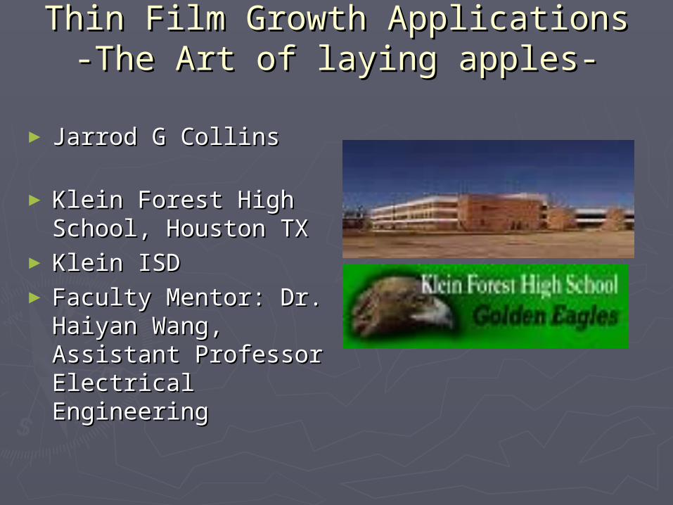
► Jarrod G Collins Jarrod G Collins
► Klein Forest High Klein Forest High School, Houston TXSchool, Houston TX
► Klein ISDKlein ISD► Faculty Mentor: Dr. Faculty Mentor: Dr.
Haiyan Wang, Haiyan Wang, Assistant Professor Assistant Professor Electrical Electrical EngineeringEngineering
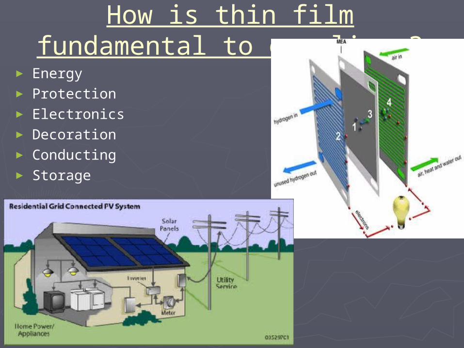
How is thin film fundamental to our lives?
► Energy► Protection► Electronics► Decoration► Conducting► Storage
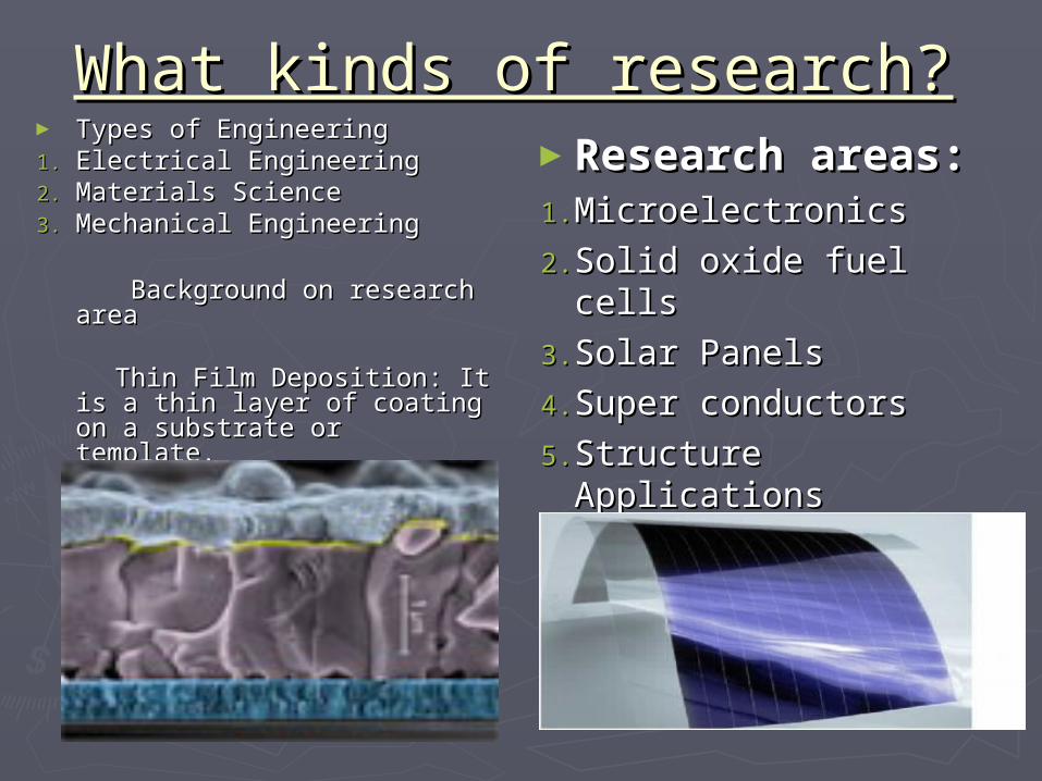
What kinds of research?What kinds of research?► Types of EngineeringTypes of Engineering1.1. Electrical EngineeringElectrical Engineering2.2. Materials ScienceMaterials Science3.3. Mechanical EngineeringMechanical Engineering
Background on research areaBackground on research area
Thin Film Deposition: It is a thin Thin Film Deposition: It is a thin layer of coating on a substrate layer of coating on a substrate or template. or template.
►Research areas:Research areas:
1.1. MicroelectronicsMicroelectronics
2.2. Solid oxide fuel cellsSolid oxide fuel cells
3.3. Solar PanelsSolar Panels
4.4. Super conductorsSuper conductors
5.5. Structure ApplicationsStructure Applications
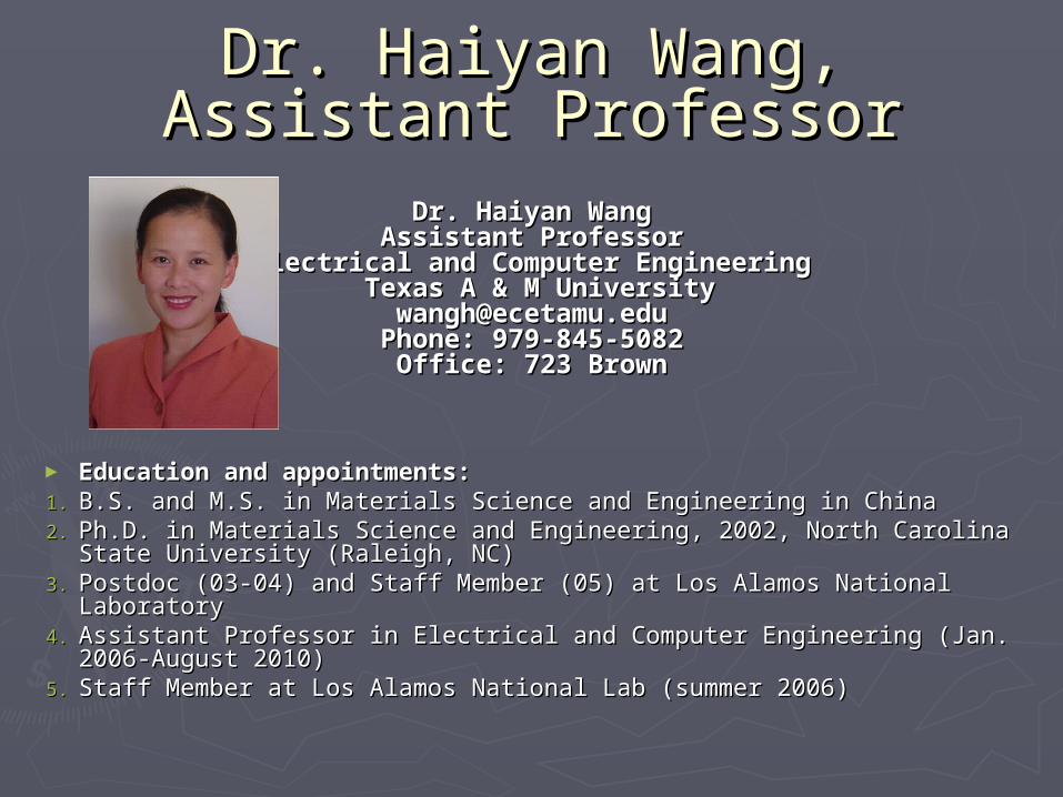
Dr. Haiyan Wang, Assistant Dr. Haiyan Wang, Assistant ProfessorProfessor
Dr. Haiyan WangDr. Haiyan WangAssistant ProfessorAssistant Professor
Electrical and Computer EngineeringElectrical and Computer Engineering Texas A & M University Texas A & M [email protected]@ecetamu.eduPhone: 979-845-5082Phone: 979-845-5082
Office: 723 BrownOffice: 723 Brown
► Education and appointments: Education and appointments: 1.1. B.S. and M.S. in Materials Science and Engineering in ChinaB.S. and M.S. in Materials Science and Engineering in China2.2. Ph.D. in Materials Science and Engineering, 2002, North Carolina State Ph.D. in Materials Science and Engineering, 2002, North Carolina State
University (Raleigh, NC)University (Raleigh, NC)3.3. Postdoc (03-04) and Staff Member (05) at Los Alamos National Postdoc (03-04) and Staff Member (05) at Los Alamos National
LaboratoryLaboratory4.4. Assistant Professor in Electrical and Computer Engineering (Jan. 2006-Assistant Professor in Electrical and Computer Engineering (Jan. 2006-
August 2010)August 2010)5.5. Staff Member at Los Alamos National Lab (summer 2006)Staff Member at Los Alamos National Lab (summer 2006)
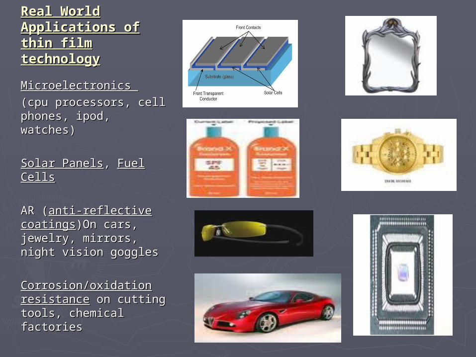
Real World Real World Applications of thin Applications of thin film technologyfilm technology
Microelectronics Microelectronics
(cpu processors, cell (cpu processors, cell phones, ipod, phones, ipod, watches)watches)
Solar PanelsSolar Panels, , Fuel CellsFuel Cells
AR (AR (anti-reflective anti-reflective coatingscoatings)On cars, )On cars, jewelry, mirrors, night jewelry, mirrors, night vision gogglesvision goggles
Corrosion/oxidation Corrosion/oxidation resistanceresistance on cutting on cutting tools, chemical tools, chemical factoriesfactories
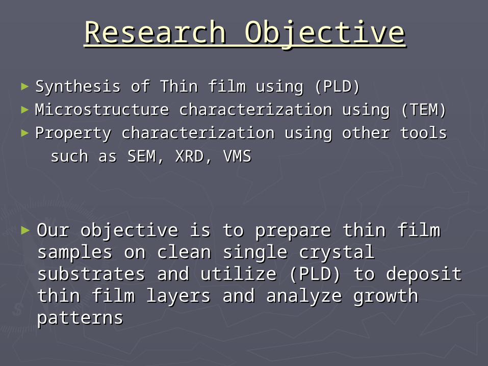
Research ObjectiveResearch Objective
►Synthesis of Thin film using (PLD)Synthesis of Thin film using (PLD)►Microstructure characterization using (TEM)Microstructure characterization using (TEM)►Property characterization using other toolsProperty characterization using other tools
such as SEM, XRD, VMSsuch as SEM, XRD, VMS
►Our objective is to prepare thin film Our objective is to prepare thin film samples on clean single crystal substrates samples on clean single crystal substrates and utilize (PLD) to deposit thin film and utilize (PLD) to deposit thin film layers and analyze growth patternslayers and analyze growth patterns

Overview of Thin Film Overview of Thin Film Deposition Deposition TechniquesTechniques
PVD (Physical Vapor Deposition)
Thermal EvaporationElectro-depositionMagnetron sputtering (DC, RF) Pulsed Laser DepositionMBE (molecular beam epitaxy)
CVD (Chemical Vapor Deposition)APCVD (atmospheric CVD)LPCVD (low-pressure CVD)PECVD (Plasma-enhanced CVD)LECVD (Laser-enhanced CVD)MOCVD (Metal-organic CVD)Solution based deposition
techniquesSol-gelPAD (Polymer assisted deposition)
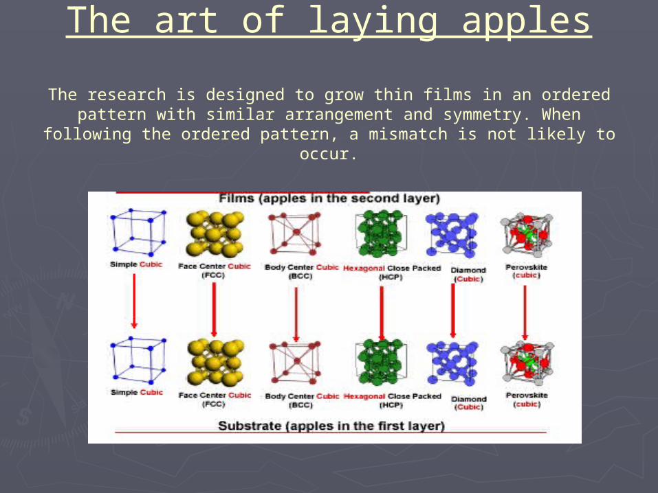
The art of laying apples
The research is designed to grow thin films in an ordered pattern with similar arrangement and symmetry. When following the ordered
pattern, a mismatch is not likely to occur.
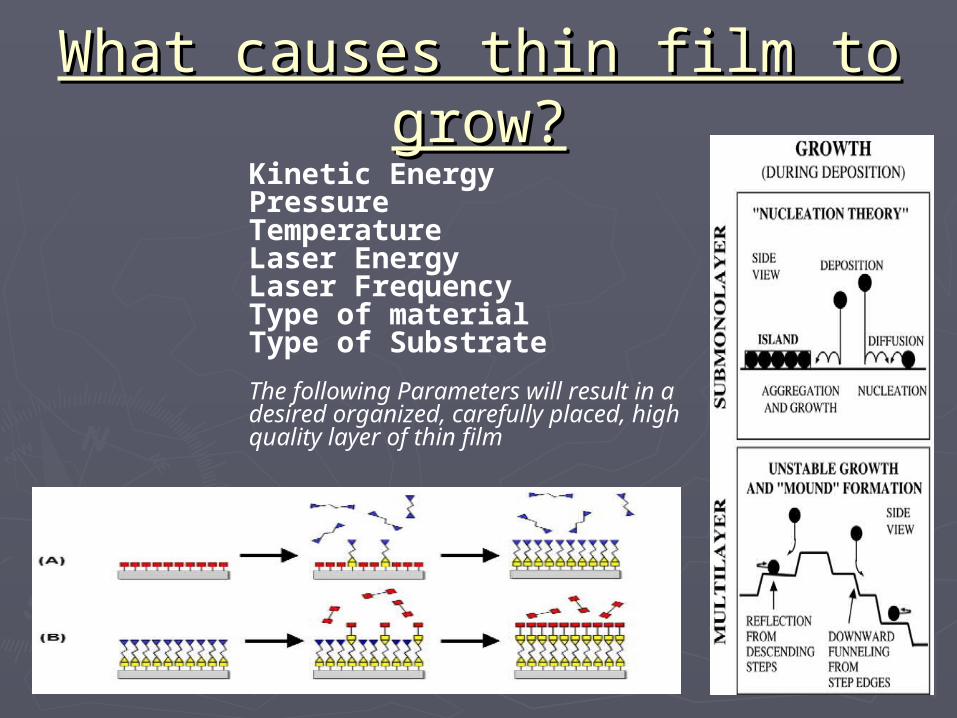
What causes thin film to What causes thin film to grow?grow?
Kinetic EnergyPressure TemperatureLaser EnergyLaser FrequencyType of material Type of Substrate
The following Parameters will result in a desired organized, carefully placed, high quality layer of thin film

Research Cycle (Data Generation)
Synthesis
Characterization
Structure & Property Correlation

Overview of MethodsOverview of MethodsSynthesisSynthesis
Pulsed Laser DepositionPulsed Laser DepositionLaser absorbs energyLaser absorbs energy
Laser evaporates targetLaser evaporates targetand deposits to substrateand deposits to substrate
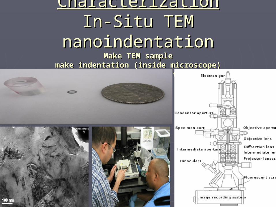
CharacterizationCharacterizationIn-Situ TEM nanoindentationIn-Situ TEM nanoindentation
Make TEM sampleMake TEM samplemake indentation (inside microscope)make indentation (inside microscope)
Analyze characteristicsAnalyze characteristics
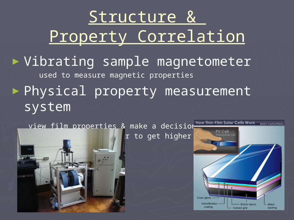
Structure & Property Correlation
►Vibrating sample magnetometer used to measure magnetic properties
►Physical property measurement system
view film properties & make a decision as to what changes need to be made in order to get higher quality films

Structure & Property Structure & Property CorrelationCorrelation
►X-ray Diffraction (XRD)X-ray Diffraction (XRD) Method of determining the arrangement of atoms in a crystalMethod of determining the arrangement of atoms in a crystal
►Scanning Electron Microscope (SEM)Scanning Electron Microscope (SEM) Powerful type of microscope, which can see objects 10,000 bigger Powerful type of microscope, which can see objects 10,000 bigger

SummarySummaryThe goal of our research is to grow high quality thin films by sustaining The goal of our research is to grow high quality thin films by sustaining an ordered foundation. The substrate needs to be a high quality single an ordered foundation. The substrate needs to be a high quality single
crystal with the same lattice structure and the same arrangement crystal with the same lattice structure and the same arrangement pattern at the right time under right conditions. pattern at the right time under right conditions.
Classroom ideasClassroom ideas
thin film creation thin film creation sunscreen concept experimentsunscreen concept experiment
painting display experimentpainting display experiment
AcknowledgementsAcknowledgements
National Science FoundationNational Science FoundationNuclear Power Institute (NPI)Nuclear Power Institute (NPI)Texas Workforce Commission (TWC)Texas Workforce Commission (TWC)Chevron corporationChevron corporationTexas A&M University Engineering departmentTexas A&M University Engineering departmentDr. Wang and Dr. ZhangDr. Wang and Dr. Zhang
Zhenxing Bi Ph.D. CandidateZhenxing Bi Ph.D. CandidateJoon Hwan Lee Ph.D. CandidateJoon Hwan Lee Ph.D. CandidateLogan Lu Ph.D. CandidateLogan Lu Ph.D. CandidateChenfong Tsai Ph.D. CandidateChenfong Tsai Ph.D. Candidate
The entire E3 facultyThe entire E3 facultyAll of the E3 ParticipantsAll of the E3 Participants

Any Questions?Any Questions?