the williams game - xmissionarcarc.xmission.com/pinball/pdf pinball misc/system 7 fix guide.pdf ·...
TRANSCRIPT

pl@P;ia 33The Williams Game

The Williams’ electronic pinball game has undergone a fair bit of evolution since itsearlier versions. It has a very capable processing system featuring lots of processing powerand includes a second microcomputer dedicated solely to sound generation. The samesystem has also been adapted for use in Williams’ Shuffle Alley games.
There are five major boards in the Williams pinball system. The first is the masterdisplay board which contains the driver circuits for the five displays and is mounted onthe insert board in the backbox. The next two are in the backbox on the left-hand side.The upper one is the CPU board and the lower is the driver board. The CPU (centralprocessing unit) board contains most of the microcomputer and outputs to the masterdisplay board, while the driver board contains the rest of the microcomputer I/O ports.These control the driving circuitry for the switch matrix, lamp matrix, and solenoids. Theoutputs to the sound board are tapped off the solenoid driver outputs. The micro-computer bus connects to the driver board via connector 1 Jl.
The fourth board, in the middle,right hand side of the backbox, is the power supplyboard containing some of the game’s fuses, the two display regulators, the +5 volt logicregulator, and some additional components of the other supplies.
Below the power supply board is mounted the fuse card which holds the fuses forthe general illumination supply and the +5 volt logic regulator. To the right are two recti-fier bridges, one for the solenoid supply and the other for the switched lamp supply. Thelarge capacitor mounted on the bottom of the backbox is the switched lamp filtercapacitor.
The fifth board is the sound board located directly above the power supply module.In earlier games this board was located in the cabinet beside the tilt assemblies and linefilter.
Connectors in the Williams game have a prefix indicating the board or circuit area,then a “P” or a “J” to indicate a male or female side, and then the pin number. Example:“3P4”.
1. POWER SUPPLIES
Primary Circuits
Power enters the Williams game through an AC cord connected to the wooden sideboard in the cabinet. The supply side connects first to the 8 ampere fast-blow (4 ampereif operated at 220 volts AC) primary fuse and then the line filter. A 130 volt rms(275Vrms at 220 volts) varistor is wired across the input to the line filter to preventvoltage spikes from entering or leaving the game. The auxiliary AC receptacle is wiredacross the AC cord before the fuse and allows for connection of trouble lights, etc. Thehot side of the supply, after the line filter, leads to the power switch and then connectsto the power transformer in the backbox via connector 6Pl together with the AC returnwire. The primaries can be connected differently to the supply wires for line voltages of105V, 117V, 210V and 235V AC. Refer to the Williams schematics for detailed infor-mation.
An earth ground braid wire is connected to ground via the line filter. The braidconnects to all external metal parts except for the ventilation hole screens. Part of thebraid connects to the backbox for grounding the circuits in the backbox and metal parts.All the circuit boards connect to ground, via their mounts and the ground braid wire,with their own mounting screws. There is no direct wire connection from the AC cord
3-l

ground to the boards themselves. This means that the cabinet braid wire must beconnected to ensure proper grounding.
AC PlugIY\
8A @ 120v4A 8 240V AC supply
1varistor
AC return
LineFilter
G N D
-Lpower switch
f
1primaries
i
l-
xxxxxxxx)(xxxxxxxxxx~ to backbox ground braid, metalparts and circuit ground.
exposed metal parts
Secondary Supplies
There are five secondary supplies in the Williams games. These are the 6.3V ACsupply for general illumination, the filtered +18V supply for the lamp matrix, the +28Vsupply for the solenoids, the 9OV AC supply which is rectified, filtered, and regulatedto provide the +lOOV and -lOOV supplies for the displays, and the 18.6V AC centre tap-ped supply. This latter supply is also regulated but to +5V for the game logic and to+12V and -12V for the sound module. These are illustrated on page 3-4.
The 6.3V AC se,condary wires from the transformer are soldered directly to the fusecard located below the power supply board. The supply side is fused with a 20A fast-blow fuse. Two pair of supply and return wires provide lamp power to the insert board.Another pair of wires provides illumination to the playfield and a fourth pair providespower to the coin slot bulbs.
The next secondary provides the +18V DC power to the lamp matrix. It is full-waverectified by the 35A 1OOPIV bridge rectifier to the lower right of the power supply boardand filtered by the large 3O,OOOpF, 25V electrolytic can capacitor mounted to the left ofthe power transformer (note that this capacitor has been incorrectly labelled 12,000 PF inthe past). Fuse protection is provided by F3, an 8A fast-blow fuse, located on the powersupply board. If the rectifier or capacitor shorts out, the primary fuse will blow.
The 25V AC secondary is full-wave rectified by the second 35A 1OOPIV rectifierbridge beside the lamp rectifier providing the +28V for the solenoids. A wire from thesolenoid rectifier leads to the power supply board. Here a O.lpF, 500V disc capacitor,lOOpF, 1OOV electrolytic capacitor, and a 30Vrms varistor are wired across the supplyoutputs. These help control any voltage spikes generated by the solenoids and not de--
3-2
spiked because of bad despiking diodes on the coils. The 1OObF capacitor gives the coilsmuch more punch when they are first energized. Any shorts in the rectifiers, the capaci-tors, or varistor should blow the primary fuse.
The flipper coils have their own 10A fast-blow fuse (15A for four flipper games)located on the power supply board. In earlier games, a second wire from the solenoidrectifier led, through a 1 pin connector, directly to the flipper fuse located under theplayfield.
The solenoid supply is also protected by a second fuse, F2, a 2.5 ampere slow-blowfuse located on the power supply board. Two wires leave the board to the rest of thegame. One provides power to the knocker and coin lockout coils in the cabinet, and thesecond provides power to the other coils under the play-field.
There are seven solenoid return wires which connect to the driver board via connec-tor 2J10, on the left hand side of the driver module.
The fourth secondary supply provides power to the display regulators. It is fusedwith Fl, a %A slow-blow fuse, located on the power supply board. The outputs of theseregulators are +lOO volts, -100 volts and -300 volts with the latter output being usedonly in the earliest games.
The fifth secondary is centre tapped and provides power to the +5 volt regulator onthe power supply board and to the separate supplies on the sound board. This latterboard has its own +5 volt regulator and unregulated +12V and -12V supplies.
The centre tap is ground referenced in both the power supply board and soundboard. The regulator module is fused with 4A slow-blow fuses mounted on the fuse card(not found in earlier games). F5 is a 4A slow-blow fuse located after the regulator’srectifiers on the power supply board. Both sides of the supply leading to the sound boardare fused with 4A slow-blow fuses on the sound board itself. In earlier games, F2 waslocated beside the sound board in the cabinet, not on the module.
The lead from the filter capacitor of the +5 volt regulator on the power supplyboard is called “+12V”, although its actual voltage may fluctuate between 9 and 12 voltsdepending upon the line voltage in the area. It is monitorred by the CPU board to detectpower-up and power-down in the system.
The +5 volt output from the power supply board connects to the master displaydriver board over one wire, to the CPU board over three wires, and to the driver boardover four wires. Similarly there are seven return wires.
Special care should be taken with the plastic strip protecting the edge of the trans-former shield. The metal has very sharp edges which can cut into any of the wires easilyand short them to ground.
+5 Volt Regulator
The main 5 volt regulator is based around a fully integrated regulator chip at X3 onthe power supply board. The 18.6 volt AC supply is fused by two 4A fuses mounted onthe fuse card below the power supply board and is then full-wave rectified by the twoMR500 types diodes 07 and 08. (As mentioned above, earlier games did not have thesefuses.) Filter capacitor Cl5 is a 12,OOOpF capacitor rated at 16V DC. With no load,there is no ripple voltage, and the capacitor is charged up to around 12 volts.
3-3
10A F.B.
F
9OV AC
Fuse Card
18.6V AC _
1cc7 CU-a-
,2x 4A S.0.
L 1
I
Power Supply Board
10A F.B.
4A S.B.
\to ground braid via t
mounting screws
w Sound Board
2 (groundbraid1
Lamp Matrix(driver board)
t
-playfield
- c a b i n e t
I//C Solenoid Drivers
(driver board)
wt1oov- l o o v1Master
DisplayGND Driver
-3oov-
r
3-4
355
3Jl
n
+!iV Regulator
I to ground connections
The logic supply fuse, F5, is rated at 4A and is a slow-blow type. In earlier games,this is the only fuse used in this supply. Capacitors Cl6 and Cl7 act as high frequencybypass capacitors and help prevent oscillation of the regulator. X3 may be replaced withan LM323K, LAS1405, or 78H05KC regulator.
Display Regulators
The display regulators are located on the power supply board. Both functionsimilarly, but with opposite polarity. The circuit is protected with Fl, a l/4 ampere,slow-blow fuse. The supply is half-wave rectified for the positive supply and half-waverectified for the negative supply by 1 N4004 type diodes D3 and D4. The supplies arefiltered by their own 100 pF, 150 volt capacitors C7 and Cl 1 which charge up to around+12OV and -120V respectively with no load.
Short circuit protection is accomplished in the regulators by providing a constantbase current,supply for the pass transistors. This base current is defined by Q2, Zl andR2 in the positive regulator and Q4, 23, and R5 in the negative regulator which act as theconstant current sources.
Zl and 23 are both 1 N5990B 3.9 volt Zener diodes. The emitter of Q2 is 0.6 voltshigher than its base voltage, and the emitter of Q4 is 0.6 volts lower than its base,meaning that 3.3 volts is applied across R2 and R5. Current flow, then, will be I = E/R= 3.3\1/680~ = 4.9mA. Most of this current is collector current which can flow througheither the 100 volt Zener diodes 22 and 24 or through the series pass transistors Ql andQ3.
Under no load conditions, the output of the regulator is open and so there can beno base current. The 1 OOV 1 N4764A Zener diodes 22 and 24 then conduct the collectorcurrent of Q2 and 04 to ground. The heat produced in the Zeners is 4.9mA x 1OOV orl/2 watt. The Zener diodes specified are rated at 1 watt to ensure reliability. -
3-5
L
351 3J5
- 9ov Fl 'D3 u
PAL +12ov +1oov
WA s.0.
+
C7 fl-1OOpF15ov
Cl11OOpF150v
23
D4 -120v
% Cl0Q3
II -300vII -
c9 D6 d
Under heavier load conditions, such as when the displays are drawing current, theemitter voltages of the pass transistors tend to drop a bit, increasing the emitter-baseforward bias voltage drops. This also tends to pull the base voltage of Ql a little lowerand the base voltage of Q3 a little higher, diverting the collector currents of Q2 and Q4away from the 100 volt Zeners. When load current increases to the point that 22 or 24current is zero, further increases in loadipg will result in *he collector voltage of Q2decreasing or the collector voltage of Q4 increasi& The pass transistors have limitedamounts of current gain, so that even with a steady 5mA of base current, their collectorcurrent won’t surpass more than about 0.2 amps, depending upon the individual transis-tors. If both regulators short at the same time, Fl will blow.
Ql should be replaced with a Motorola type SDS201 NPN transistor and Q3 witha type SDS202 PNP transistor.
D4, D5, D6, C9 and Cl0 are intended to function as a voltage triplet-. Diode D5prevents the output side of C9 from increasing above the filter capacitor voltage of about-125 volts. However, C9 AC couples the full peak to peak voltage of the AC supply toD6 which charges ClO. The voltage on Cl0 will be equal to the ripple voltage on Cl 1plus the peak-to-peak AC voltage of the supply. This will be (--12OV) + (-240V) = -360volts. However, the efficiency of this typ,e of circuit is poor and the output voltage ismore likely to be around -320 volts.
The -300 volt supply was used in the earlier games to help ionize the gas in thedisplay tubes but is not used in present displays.
3-6 I
..-
2. MASTER DISPLAY DRIVER BOARD
The master display driver board provides the decoding and driving functions for thefive 6 digit, seven segment gas discharge display tubes. The CPU board provides 16 digitstrobes and two sets of BCD data to the master display driver. The displays are matrixedwith BCD data group 1 controlling the cathode segments of players 1 and 2 and the statusdisplays and with BCD data group 2 controlling players 3 and.4.
Digit strobes 1 through 6 control player 1 and 3 digit anodes, starting with the100,000s column as digit strobe 1. Digits 9 through 14 control the 2nd and 4th playerdigits, and digits 15, 16, 7, and 8 control the status display.
Digit Strobes
BCDl
BCD 2
123456 9 1011121314 16 16 7 8
- Decoder 1= IC3 o r IC6 H’K
cathode drivers
There are two types of master display boards used by Williams. The earlier typeused IC drivers while the newer ones use discrete transistor drivers. The switch-over grewout of problems Williams had in obtaining sufficient quantities of their IC drivers. We willlook at the earlier system first.
Old Display Driver Board
There are four types of integrated circuits used on the earlier board. These are thedigit drivers, segment drivers, BCD to 7 segment decoders, and CMOS inverters. Provisionwas made to allow the replacement of the first three parts with alternate parts in theevent of difficulty in obtaining parts.
Either a Sprague UDN6184 or Signetics NE585 octal anode driver, or equivalent,may be used in locations IC4, ICl 1, IC12, or IC13. The NE585 are 22 pin chips andrequire ZRl, a lN6000B 10 volt Zener diode and resistor R22 if one or more of theseparts are used. The UDN6184s are 20 pin chips and are not affected by the use of ZRl.
Either a Sprague UDN7180 or Signetics NE584 octal cathode driver, or equivalent,may be used in locations IC9 or IClO. The NE584 requires a 91 k pull-down resistor onpin 12 on each of these chips that may be used. These are 22 pin parts. The UDN7180 isa 20 pin device.
3-7
The two possible BCD to seven segment decoders which can be used are both 16 pinCMOS parts but have different pins used for inputs and outputs. The 45438 is used inlocations IC5 and IC8. The 45588 can be used in locations IC6 and IC7. The differentlocations have the traces connected differently to take into account the pin differences.As the segment patterns for the three digits “l”, “6”, and “9” are output differently inthe two decoders, it is recommended that only one type of decoder be used in each board.
The fourth type of part is the CMOS 40698 inverters located at ICl, IC2 and IC3.These are used to invert the digit strobe data from the CPU board and invert the blankingsignal for the 45438 type decoder chip. The Blanking line turns off the displays in theevent of a malfunction on the CPU board as well as during power-up and power-down.
The digit drivers act as buffer amplifiers, whereas the segment (cathode) drivers actas inverters.
Blanking
New Display Driver Board
The block layout of the newer master display board is similar to the layout of theolder board but with several important differences.
Sixteen 4069B CMOS inverters are used as input inverting buffers from the CPUboard for the digit strobes. An MPSA42 transistor inverts the output from each gate andacts as a level shifter for the MPSA92 driver. Since only one of the level shifter transis-tors is on at a time, one single 270Q resistor is shared between all sixteen of the transis-tors. This lets the outputs of the CMOS inverters go HIGH, yet still allows the transistors’ . .to maintain a 0.6V drop from base to emitter.
3-8

L
57
+1()ov
J5-
-
J6-
output via
1x161
Digit Strobe Line
+5v+gv I
L
IL=
2.2k
r
c Blanking
from otherdecoder’s inputs
- l O O v
1, J2, 53, & J4
Display Tuba_-----
A
IPS-A42
Ik
-TToutput viaJl, J2, J3, 81 54
3-9

The 8.2k and 10k resistors are used to turn ON and turn OFF, respectively, theMPS-A92 driver. The clamp diode on the driver’s collector protects the transistor fromexposure to negative voltage spikes which may be applied to the anode due to thenegative voltages on the segment cathodes in the display tube.
The cathode drivers are controlled by the segment output pins of the 45438 de-coders. The emitter supply for the fourteen MPS-A92 level shifters in this circuit is att3.8 volts and is derived from the t5V logic supply through two silicon diodes. Since the45438’s output HIGH voltage is close to t5 volts, this guarantees quick turn OFF of theA92s. The 47k and 2.2k resistors, respectively, turn ON and OFF the MPS-A42 segmentdrivers. When the level shifter transistor is turned ON, its collector voltage is approxi-mately t3.4V. The 47k and 2.2k resistors now have 103.4 volts across them and dividethis to about -95.4 volts at the driver’s base, which is 4.6 volts higher than the -lOOVsupply. Allowing for the emitter base drop, the 1 k resistor has about 4 volts across itselfwith a current of I = E x R, or about 4mA, through it. This of course makes this a cur-rent switching circuit rather than a voltage switching circuit.
The 100k resistor from the driver’s collector to ground helps to discharge the smallamount of cathode and transistor capacitance to ground. The clamp diode protects thedriver against positive voltage spikes contributed by the anode drivers through the displaytube.
A 40128 CMOS dual Qinput NAND gate is used on this board to control the blank-ing inputs of the 45438 decoders. If the Blanking signal from the CPU board goes LOW,or if the connectors are disconnected from the CPU board, the blanking inputs on thedecoder are raised HIGH, turning OFF all the displays.
The other 4-input NAND gate connects to the 8s and 4s inputs of both decoders. Ifthe CPU board sends out all HIGHS on these lines, between strobe signals, (correspondingto decimal values of twelve or higher), the blanking inputs are also raised HIGH, turningOFF the decoders. The combination 100k resistor and 47OpF capacitor prolongs thedecoders’ blanking signal until all the BCD data is latched into the master display boardand the digits are set up again.
3.. CPU BOARD
Page 3-l 1 shows the general architecture of the new Williams microcomputer. Mostof it is on the CPU board but the last three sets of l/D chips, called PIAs, are located onthe driver board. Because of the number of parts on the bus, bus drivers and bus trans-ceivers are utilized to help drive the bus lines to the proper threshold levels quickly andcleanly.
The CPU board underwent a major revision affecting four main areas in 1979. Theseare the type of microprocessor used, a redesign of the reset circuitry, a redesign of theinterrupt generator, and improvements in the CMOS RAM memory protection circuitry.
Power
Connector 1 J2, on the upper left hand side of the CPU board, provides the unregula-ted t12 volts of the t5 volt regulator over one wire, and t5 volt supply and return overthree pairs of wires. The +5V is the logic supply and the unregulated t12V (labelled +9V
3-10
cl;
AddressBuffer
-4. c
diagnostic switch
t Data Bus Transceiver Data E
I r-l r-l
ICY M i c r o p r o c e s s o r u w 1
IC17 ROM
I-_?1lC20 R O M
I
I
I
I
1
I
I
I
ICll PIA II (Driver Board)
IClO PIA III (Driver Board)
IC5 PIA IV IDriver Board )
in some Williams schematics) is used by the reset circuits to detect power-up and power-down. Test points TP9, TPlO, and TPl, on the new boards, allow quick access to +5V,ground, and +12V respectively.
Reset Circuits
The reset circuit disables the CMOS bookkeeping RAM during power-down, providesa reset signal to the microprocessor at power-up, and also resets the I/O ports to the highimpedance state when power is off.
filter capacitor
System Reset
Reset Circuit - Old Board
The old reset circuit involved four smaller circuit areas. The first one detected avalid power condition. The t5 volt regulator requires t7V or more on its input toproduce a clean t5.0 volt output. ZRl is a 1 N5996B Zener diode rated at 6.8 volts andmonitors the five volt regulator capacitor. When the capacitor voltage increases past 6.8volts, a voltage appears across R29 and R27. Q2 and Q3 are switched ON at about 7.3V,by which time the logic regulator is outputting a good t5.0 volts. When power is lost, Q2,Q3 and Q6 switch OFF before the t5.0 volt logic supply is lost.
When Q3 is ON, Q4 is turned ON and the CMOS RAM is then powered by the +5Vlogic supply rather than the batteries. Ordinary 1.5 volt alkaline cells are used and shouldbe replaced once a year. Diode D17 prevents damage to the batteries when game poweris ON. Diode D18 prevents the batteries from discharging through the base collectorjunction of Q4 when logic power is OFF.
When Q2 is ON, both Ql and Q6 are turned OFF. R2 then pulls the System Resetline HIGH, signalling lC5 to pull its Reset line HIGH, starting the MPU and PIAs. Cl is a22pF tantalum capacitor which, together with R2, delays the System Reset signal for halfa second at power-up. Q6 controls the CE2 of the CMOS RAM, IC9. When Q6 is ON -atpower-up and power-down- it keeps the RAM disabled.
3-l 2
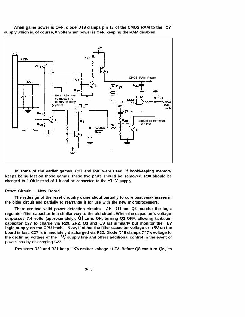
When game power is OFF, diode Dl9 clamps pin 17 of the CMOS RAM to the t5Vsupply which is, of course, 0 volts when power is OFF, keeping the RAM disabled.
lJ2
I
CMOS RAM Power+
I Note: R30 was L -connected to
f
to t5V in earlygames. p_F
t5vI
Ishould be
see textremoved
In some of the earlier games, C27 and R40 were used. If bookkeeping memorykeeps being lost on those games, these two parts should be’ removed. R30 should bechanged to 1 Ok instead of 1 k and be connected to the +12V supply.
Reset Circuit - New Board
The redesign of the reset circuitry came about partially to cure past weaknesses inthe older circuit and partially to rearrange it for use with the new microprocessors.
There are two valid power detection circuits. ZRl, Ql and Q2 monitor the logicregulator filter capacitor in a similar way to the old circuit. When the capacitor’s voltagesurpasses 7.4 volts (approximately), Ql turns ON, turning Q2 OFF, allowing tantalumcapacitor C27 to charge via R29. ZR2, Q3 and Q9 act similarly but monitor the t5Vlogic supply on the CPU itself. Now, if either the filter capacitor voltage or t5V on theboard is lost, C27 is immediately discharged via R32. Diode D19 clamps C27’s voltage tothe declining voltage of the +5V supply line and offers additional control in the event ofpower loss by discharging C27.
Resistors R30 and R31 keep Q8’s emitter voltage at 2V. Before Q8 can turn ON, its
3-l 3
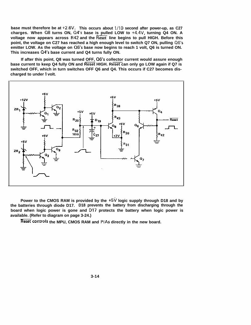
base must therefore be at +2.6V. This occurs about l/10 second after power-up, as C27charges. When Q8 turns ON, Q4’s base is pulled LOW to +4.4V, turning Q4 ON. Avoltage now appears across R42 and the Reset line begins to pull HIGH. Before thispoint, the voltage on C27 has reached a high enough level to switch Q7 ON, pulling Q6’semitter LOW. As the voltage on Q6’s base now begins to reach 1 volt, Q6 is turned ON.This increases Q4’s base current and Q4 turns fully ON.
If after this point, Q8 was turned OFF, Q6’s collector current would assure enoughbase current to keep Q4 fully ON and Reset HIGH. Reset can only go LOW again if Q7 isswitched OFF, which in turn switches OFF Q6 and Q4. This occurs if C27 becomes dis-charged to under 1 volt.
+5v+5v
+5v
2R2
~_----_~
%Q7
c
Power to the CMOS RAM is provided by the +5V logic supply through D18 and bythe batteries through diode D17. D18 prevents the battery from discharging through theboard when logic power is gone and 017 protects the battery when logic power isavailable. (Refer to diagram on page 3-24.)
Reset controls the MPU, CMOS RAM and PlAs directly in the new board.
3-14

System Clock - Old Board
The old CPU board uses a Motorola MC6875 clock chip at IC5 and a 3.58 MHzcolour television crystal’to produce the 2-phase clock outputs and control the board’sReset line.
Rl, Ll and C66 make up a “tank” circuit which helps stabilize the oscillator duringpower-up. The oscillator frequency is divided by four, internally, to about 900 kHz.41 and 42 are of opposite phase and drive the MPU’s clock inputs. “Bus$~” is in thesame phase as (02 but is used for timing in the rest of the microcomputer. The SystemReset output from the reset circuits is input to IC5. A low impedance output buffercontrols the -line which controls the MPU and other parts on the board.
Crystal o
1
6675
- N.C. Bus 92 IO.lpF
(not
= - N.C.
G===~TGziii
= included inall games)
1 t, Ito rest of
board
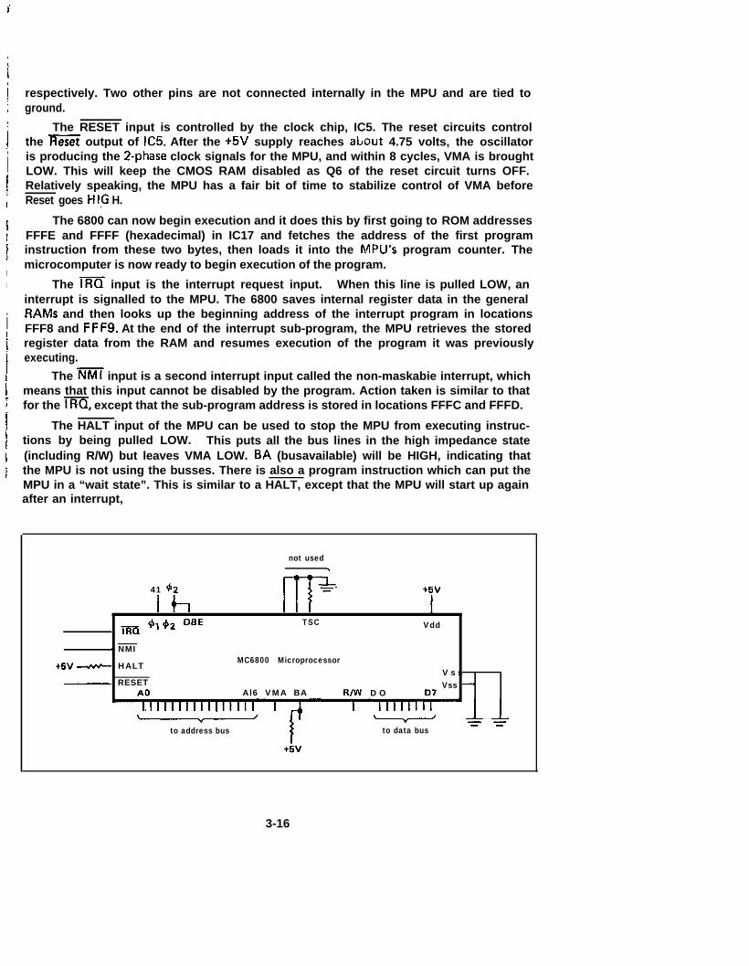
Motorola MC6800 Microprocessor - Old Board
The Motorola MC6800 MPU is an 8 bit microprocessor with 16 address lines. Theaddress lines often output erratic values and so, a VMA line (valid memory address) out-put is used by the address decoding circuit to select memory devices only when there is avalid memory address on the bus (VMA is HIGH).
The R/W line is LOW for a write and HIGH the rest of the time. The eight data linesare bidirectional and are in the high impedance state whenever DBE (data bus enable) isLOW or the R/W line is HIGH.
A new address is put out on the address bus about 200 to 300 nsec after 92 (andBus@2 goes LOW. Data transfers occur three quarters of a cycle later when 42 makesa negative transition again. (The maximum clock frequency of the 6800 is 1 MHz.)
The 6800 operates off +5 volts and has two ground connections. Two of the MPU’spins are not used in the Williams’ system (Halt and TSC) and are tied HIGH and LOW
3-l 5
i
L
;
i
,
I
1i1I
I
1,,
iI!jIIIi
respectively. Two other pins are not connected internally in the MPU and are tied toground.
The RESET input is controlled by the clock chip, IC5. The reset circuits controlthe Reset output of IC5. After the +5V supply reaches aLout 4.75 volts, the oscillatoris producing the 2-phase clock signals for the MPU, and within 8 cycles, VMA is broughtLOW. This will keep the CMOS RAM disabled as Q6 of the reset circuit turns OFF.Relatively speaking, the MPU has a fair bit of time to stabilize control of VMA beforeReset goes H IG H.
The 6800 can now begin execution and it does this by first going to ROM addressesFFFE and FFFF (hexadecimal) in IC17 and fetches the address of the first programinstruction from these two bytes, then loads it into the MPU’s program counter. Themicrocomputer is now ready to begin execution of the program.
The IRQ input is the interrupt request input. When this line is pulled LOW, aninterrupt is signalled to the MPU. The 6800 saves internal register data in the generalRAMS and then looks up the beginning address of the interrupt program in locationsFFF8 and FFFS. At the end of the interrupt sub-program, the MPU retrieves the storedregister data from the RAM and resumes execution of the program it was previouslyexecuting.
The NMI input is a second interrupt input called the non-maskabie interrupt, whichmeans that this input cannot be disabled by the program. Action taken is similar to thatfor the m, except that the sub-program address is stored in locations FFFC and FFFD.
The HALT input of the MPU can be used to stop the MPU from executing instruc-tions by being pulled LOW. This puts all the bus lines in the high impedance state(including R/W) but leaves VMA LOW. 8A (busavailable) will be HIGH, indicating thatthe MPU is not using the busses. There is also a program instruction which can put theMPU in a “wait state”. This is similar to a HALT, except that the MPU will start up againafter an interrupt,
not used\
41 42 +5v
ItI 1
_ m 4142 DBE TSC Vdd
-- NMI
t5V e HALT MC6800 MicroprocessorV s s
- RESET Vss -A0 Al6 VMA BA R/W D O 07
to address bus to data bus
3-16
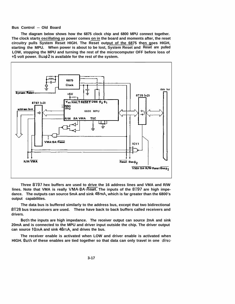
Bus Control - Old Board
The diagram below shows how the 6875 clock chip and 6800 MPU connect together.The clock starts oscillating as power comes on in the board and moments after, the resetcircuitry pulls System Reset HIGH. The Reset output of the 6875 then goes HIGH,starting the MPU. When power is about to be lost, System Reset and Reset are pulledLOW, stopping the MPU and turning the rest of the microcomputer OFF before loss of+5 volt power. Bus42 is available for the rest of the system.
data bur
6600 MPU
Three 8T97 hex buffers are used to drive the 16 address lines and VMA and R/Wlines. Note that VMA is really VMARA.Reset. The inputs of the 87-97 are high impe-dance. The outputs can source 5mA and sink 48mA, which is far greater than the 6800’soutput capabilities.
The data bus is buffered similarly to the address bus, except that two bidirectional8T28 bus transceivers are used. These have back to back buffers called receivers anddrivers.
Both the inputs are high impedance. The receiver output can source 2mA and sink20mA and is connected to the MPU and driver input outside the chip. The driver outputcan source 10mA and sink 48mA, and drives the bus.
The receiver enable is activated when LOW and driver enable is activated whenHIGH. Both of these enables are tied together so that data can only travel in one direc-
3-17
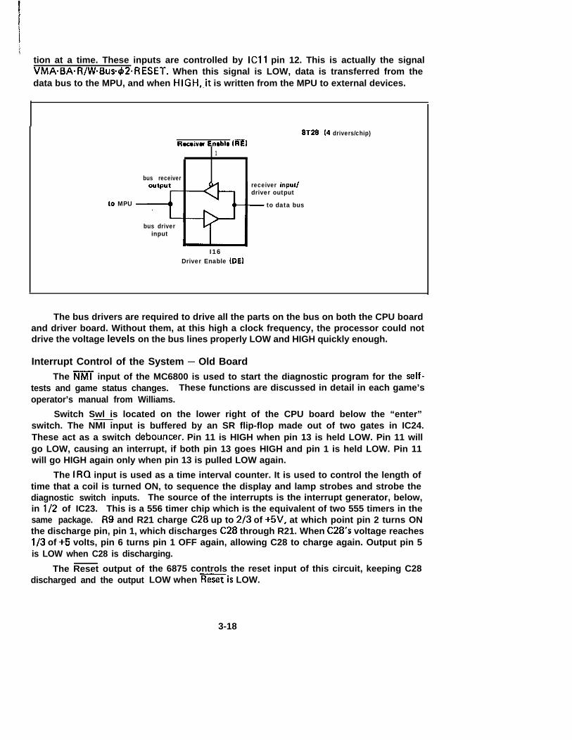
tion at a time. These inputs are controlled by ICll pin 12. This is actually the signalVMA.BA.R/W.BU~~~.RESET. When this signal is LOW, data is transferred from thedata bus to the MPU, and when HIGH,,it is written from the MPU to external devices.
to MPU
Rmcaivr Enrblo (m)1
bus receiver
bus driverinput
I16Driver Enable (DE)
a‘T28 (4 drivers/chip)
receiver input/driver output
- to data bus
The bus drivers are required to drive all the parts on the bus on both the CPU boardand driver board. Without them, at this high a clock frequency, the processor could notdrive the voltage levels on the bus lines properly LOW and HIGH quickly enough.
Interrupt Control of the System - Old BoardThe NMI input of the MC6800 is used to start the diagnostic program for the self-
tests and game status changes. These functions are discussed in detail in each game’soperator’s manual from Williams.
Switch Swl is located on the lower right of the CPU board below the “enter”switch. The NMI input is buffered by an SR flip-flop made out of two gates in IC24.These act as a switch debouncer. Pin 11 is HIGH when pin 13 is held LOW. Pin 11 willgo LOW, causing an interrupt, if both pin 13 goes HIGH and pin 1 is held LOW. Pin 11will go HIGH again only when pin 13 is pulled LOW again.
The IRQ input is used as a time interval counter. It is used to control the length oftime that a coil is turned ON, to sequence the display and lamp strobes and strobe thediagnostic switch inputs. The source of the interrupts is the interrupt generator, below,in l/2 of IC23. This is a 556 timer chip which is the equivalent of two 555 timers in thesame package. R9 and R21 charge C2B up to 2/3 of +5V, at which point pin 2 turns ONthe discharge pin, pin 1, which discharges C2B through R21. When C28’s voltage reachesl/3 of +5 volts, pin 6 turns pin 1 OFF again, allowing C28 to charge again. Output pin 5is LOW when C28 is discharging.
The Reset output of the 6875 controls the reset input of this circuit, keeping C28discharged and the output LOW when eis LOW.
3-18

CA1 and CBl inputs
diagnostic switches(front door)
4O~seCk lmsec -_1 -I I-
lntorrupt Generator Output
; I
Display Strobe I I I
’ II I
l II Il I
Display Strobe, etc. I I1 I
II .
1 I
l II
Lamp Strobe 1 t- strobe ON
Lamp Return
Switch Strobe - Old Board
Stitch Strobe - New Board
3-19
The interrupt generator runs at a frequency of about 1,100 Hz and the output signalhas a period of about 900 p sec.
Note in the facing diagram that the PlAs (described on page 3-26) do not interruptthe MPU. Instead, PIA I is checked by the main program automatically through the databus and internal registers of the PIA. The CA1 and CBl interrupt inputs are used then,as input switch latches for the front door diagnostic switches.
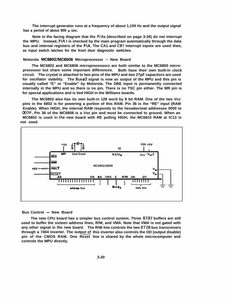
Motorola MC6802/MC6808 Microprocessor - New Board
The MC6802 and MC6808 microprocessors are both similar to the MC6800 micro-processor but share some important differences. Both have their own built-in clockcircuit. The crystal is attached to two pins of the MPU and two 27pF capacitors are usedfor oscillator stability. The Bus+2 signal is now an output of the MPU and this pin isusually called “E” or “Enable” by Motorola. The DBE input is permanently connectedinternally in the MPU and so there is no pin. There is no TSC pin either. The MR pin isfor special applications and is tied HIGH in the Williams boards.
The MC6802 also has its own built-in 128 word by 8 bit RAM. One of the two Vccpins in the 6802 is for powering a portion of this RAM. Pin 36 is the “RE” input (RAMEnable). When HIGH, the internal RAM responds to the hexadecimal addresses 0000 to007F. Pin 36 of the MC6808 is a Vss pin and must be connected to ground. When anMC6802 is used in.the new board with RE pulling HIGH, the MC6810 RAM at IC13 is
not used.
+sv +!iv +5v
I 36 I I
iimMR Xtal Extal R El&s Vcc’ VCG
dimi,
+svw HALfMC680218808
VS.5- RESET Vss -
A0 Al6 BA VMA E R/W DO D7
\llllllllllllllll 1
, I I -I --rddrass bus -42
.I I I ‘,’ I I I Jdata bus c=
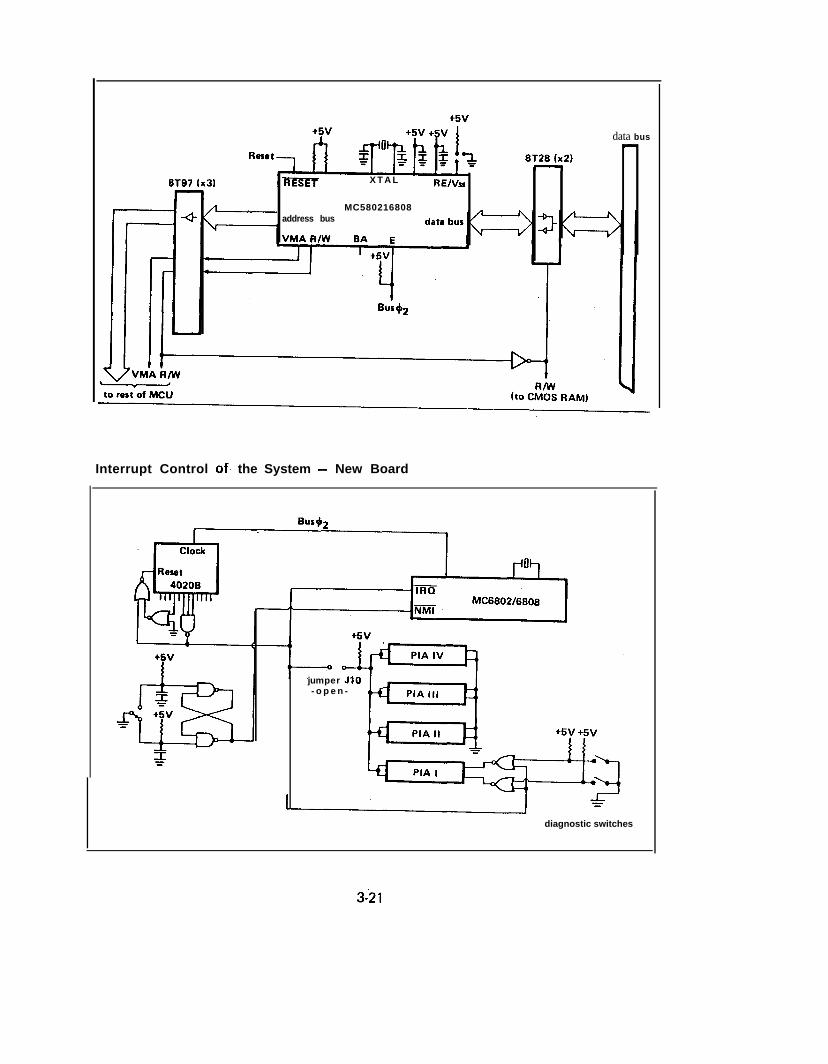
Bus Control - New Board
The new CPU board has a simpler bus control system. Three 8T97 buffers are stillused to buffer the sixteen address lines, R/W, and VMA. Note that VMA is not gated withany other signal in the new board. The R/W line controls the two 8T28 bus transceiversthrough a 7404 inverter. The output ofpin of the CMOS RAM. One Resetcontrols the MPU directly.
this inverter also controls the OD (output disable)line is shared by the whole microcomputer and
3-20
8T97 (x3)
t5v
data bus-
Resrt 8T28 (~21-
X T A L REIVS
MC580216808address bus
Interrupt Control of, the System - New Board
jumper JlO- o p e n -
diagnostic switches
3-21
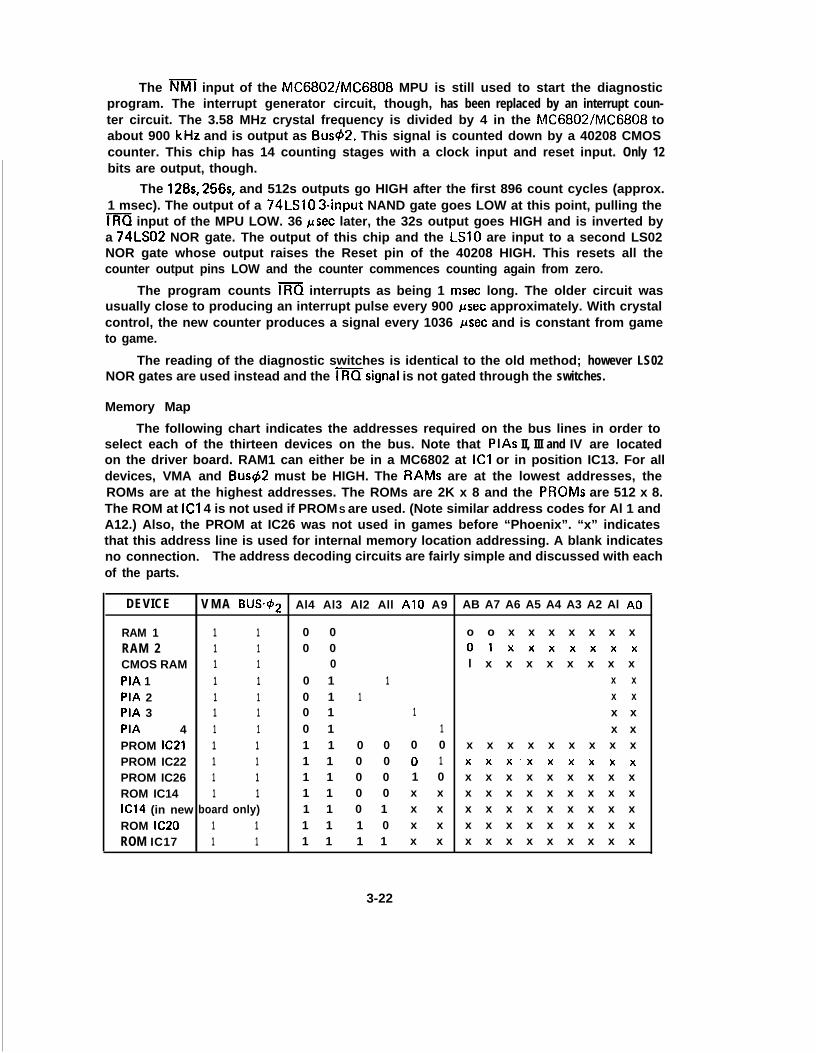
The NMI input of the MC6802/MC6808 MPU is still used to start the diagnosticprogram. The interrupt generator circuit, though, has been replaced by an interrupt coun-ter circuit. The 3.58 MHz crystal frequency is divided by 4 in the MC6802/MC6808 toabout 900 kHz and is output as Bus92. This signal is counted down by a 40208 CMOScounter. This chip has 14 counting stages with a clock input and reset input. Only 12bits are output, though.
The 128s, 256s, and 512s outputs go HIGH after the first 896 count cycles (approx.1 msec). The output of a 74LSlO 3-input NAND gate goes LOW at this point, pulling theIRQ input of the MPU LOW. 36 psec later, the 32s output goes HIGH and is inverted bya 74LSO2 NOR gate. The output of this chip and the LSlO are input to a second LS02NOR gate whose output raises the Reset pin of the 40208 HIGH. This resets all thecounter output pins LOW and the counter commences counting again from zero.
The program counts IRQ interrupts as being 1 msec long. The older circuit wasusually close to producing an interrupt pulse every 900 psec approximately. With crystalcontrol, the new counter produces a signal every 1036 clsec and is constant from gameto game.
The reading of the diagnostic switches is identical to the old method; however LS02NOR gates are used instead and the msignal is not gated through the switches.
Memory Map
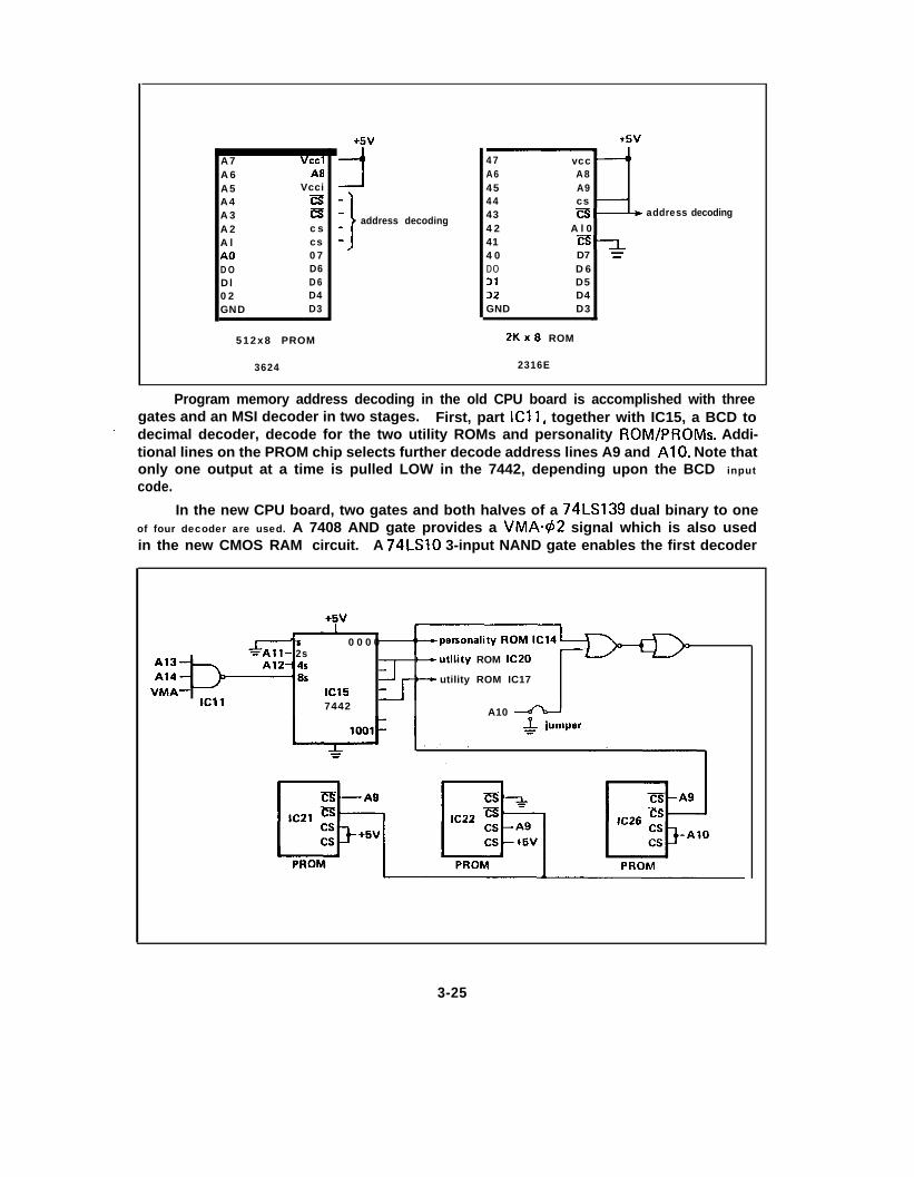
The following chart indicates the addresses required on the bus lines in order toselect each of the thirteen devices on the bus. Note that PlAs II, III and IV are locatedon the driver board. RAM1 can either be in a MC6802 at ICl or in position IC13. For alldevices, VMA and Bus@2 must be HIGH. The RAMS are at the lowest addresses, theROMs are at the highest addresses. The ROMs are 2K x 8 and the PROMS are 512 x 8.The ROM at ICY 4 is not used if PROM S are used. (Note similar address codes for Al 1 andA12.) Also, the PROM at IC26 was not used in games before “Phoenix”. “x” indicatesthat this address line is used for internal memory location addressing. A blank indicatesno connection. The address decoding circuits are fairly simple and discussed with eachof the parts.
DEVICE V M A BUS+2 Al4 Al3 Al2 All Al0 A9 AB A7 A6 A5 A4 A3 A2 Al A0
RAM 1 1 1 0 0 o o x x x x x x xRAM 2 1 1 0 0 01xxxxxxxCMOS RAM 1 1 0 l x x x x x x x x
PIA 1 1 1 0 1 1 x x
PIA 2 1 1 0 1 1 x xPIA 3 1 1 0 1 1 x xPIA 4 1 1 0 1 1 x xPROM lC21 1 1 1 1 0 0 0 0 x x x x x x x x xPROM IC22 1 1 1 1 0 0 0 1 xxx’xxxxxxPROM IC26 1 1 1 1 0 0 1 0 x x x x x x x x xROM IC14 1 1 1 1 0 0 x x x x x x x x x x xIC14 (in new board only) 1 1 0 1 x x x x x x x x x x xROM IC20 1 1 1 1 1 0 x x x x x x x x x x xROM IC17 1 1 1 1 1 1 x x x x x x x x x x x
3-22
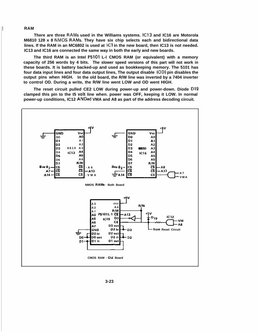
I RAM
There are three RAMS used in the Williams systems. ICI3 and IC16 are MotorolaM6810 128 x 8 NMOS, RAMS. They have six chip selects each and bidirectional datalines. If the RAM in an MC6802 is used at ICl in the new board, then IC13 is not needed.IC13 and IC16 are connected the same way in both the early and new boards.
The third RAM is an Intel P5101 L-l CMOS RAM (or equivalent) with a memorycapacity of 256 words by 4 bits. The slower speed versions of this part will not work inthese boards. It is battery backed-up and used as bookkeeping memory. The 5101 hasfour data input lines and four data output lines, The output disable (OD) pin disables theoutput pins when HIGH. In the old board, the R/W line was inverted by a 7404 inverterto control OD. During a write, the R/W line went LOW and OD went HIGH.
The reset circuit pulled CE2 LOW during power-up and power-down. Diode D19clamped this pin to the t5 vo’lt line when. power was OFF, keeping it LOW. In normalpower-up conditions, IC12 ANDed VMA and A8 as part of the address decoding circuit.
-I_z DO A0 &---
Dl A lD2 A 203 6 6 1 0 A 3D4D5
IC13 ;;
D6 A 607 A/w
Bw+~- cs = - A 6A7- i!% = -A13
Bus+~ -
A14- = C6 - V M A --r;l4/ \
NMOS RAMS - Both Board
+5v
IGNDIDO
VccA0-rDl A l
ID2ID3 6610 :‘3
A 7V M A
+5v
A 3 vccA 2 A 4 R/w
A l R/W 0+5v
Dl9
+I++from
IC12
--a=::
Reset Circuit
CMOS RAM -Old Board
3-23
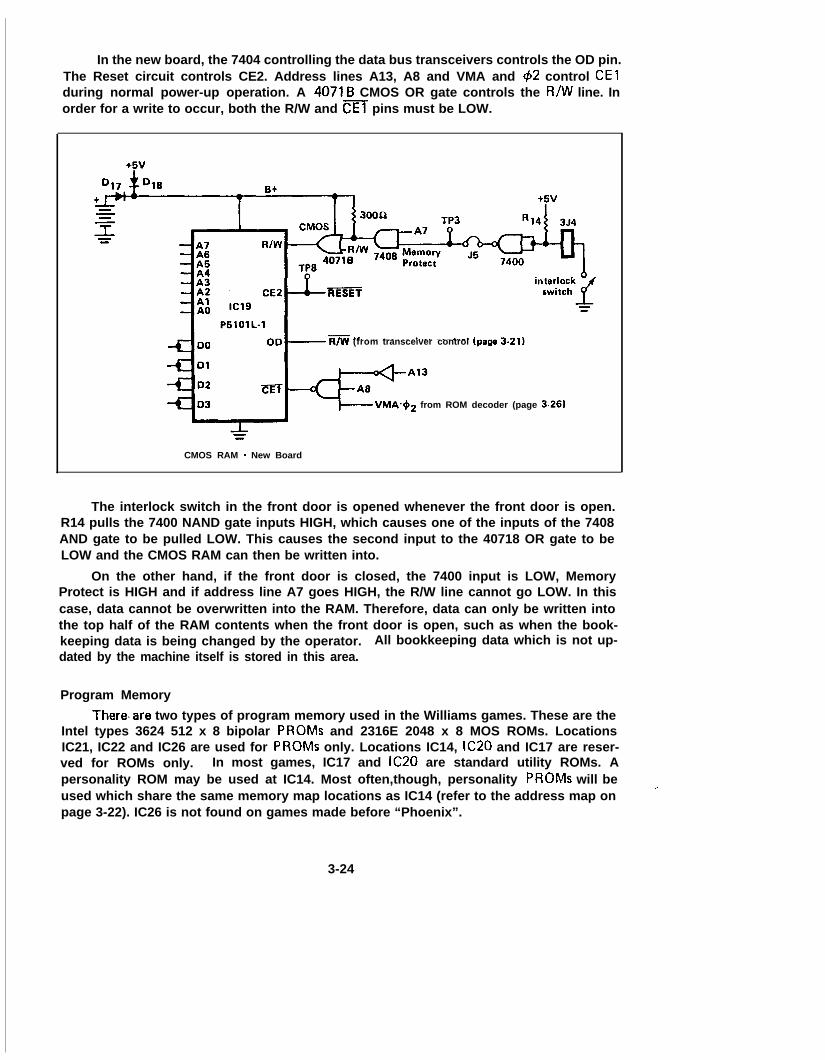
In the new board, the 7404 controlling the data bus transceivers controls the OD pin.The Reset circuit controls CE2. Address lines A13, A8 and VMA and 92 control CElduring normal power-up operation. A 40718 CMOS OR gate controls the R/W line. Inorder for a write to occur, both the R/W and CEI pins must be LOW.
R/W (from transceiver control (page 3-21)
VMA*+Z from ROM decoder (page 3-26)
CMOS RAM - New Board
The interlock switch in the front door is opened whenever the front door is open.R14 pulls the 7400 NAND gate inputs HIGH, which causes one of the inputs of the 7408AND gate to be pulled LOW. This causes the second input to the 40718 OR gate to beLOW and the CMOS RAM can then be written into.
On the other hand, if the front door is closed, the 7400 input is LOW, MemoryProtect is HIGH and if address line A7 goes HIGH, the R/W line cannot go LOW. In thiscase, data cannot be overwritten into the RAM. Therefore, data can only be written intothe top half of the RAM contents when the front door is open, such as when the book-keeping data is being changed by the operator. All bookkeeping data which is not up-dated by the machine itself is stored in this area.
Program Memory
There.are two types of program memory used in the Williams games. These are theIntel types 3624 512 x 8 bipolar PROMS and 2316E 2048 x 8 MOS ROMs. LocationsIC21, IC22 and IC26 are used for PROMS only. Locations IC14, IC20 and IC17 are reser-ved for ROMs only. In most games, IC17 and IC20 are standard utility ROMs. Apersonality ROM may be used at IC14. Most often,though, personality PROMS will beused which share the same memory map locations as IC14 (refer to the address map onpage 3-22). IC26 is not found on games made before “Phoenix”.
3-24
A7 VcclA 6 A8A5 VcciA4 izA 3 i%A 2 c sAl csA0 07DO D6Dl D602 D4GND D3
i5V
II
address decoding
47A64544434 2414 0DODlD2GND
vcc -’A8A9cs -CS- c address decoding
A l 0ES--J_D7 ED 6D5D4D3
.
512x8 PROM 2Kx8 ROM
3624 2316E
+5v
Program memory address decoding in the old CPU board is accomplished with threegates and an MSI decoder in two stages. First, part ICl 1, together with IC15, a BCD to
. decimal decoder, decode for the two utility ROMs and personality ROM/PROMS. Addi-tional lines on the PROM chip selects further decode address lines A9 and AlO. Note thatonly one output at a time is pulled LOW in the 7442, depending upon the BCD inputcode.
In the new CPU board, two gates and both halves of a 74LS139 dual binary to oneof four decoder are used. A 7408 AND gate provides a VMA.42 signal which is also usedin the new CMOS RAM circuit. A 74LSlO 3-input NAND gate enables the first decoder
1s&All- 2s
0 0 0 0
Al3-) : -utility ROM IC20
Al4- utility ROM IC17VMA- ICl5
ICll 7442 A10 -a”~-
3-25
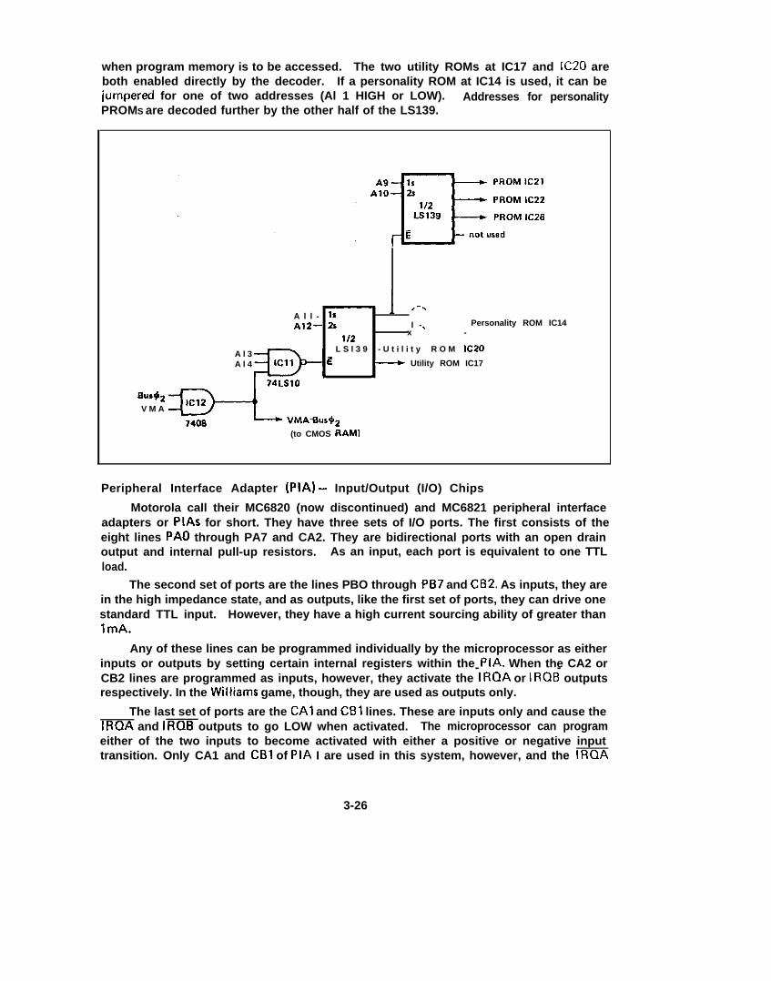
when program memory is to be accessed. The two utility ROMs at IC17 and IC20 areboth enabled directly by the decoder. If a personality ROM at IC14 is used, it can bejumpered for one of two addresses (Al 1 HIGH or LOW). Addresses for personalityPROMS are decoded further by the other half of the LS139.
r-xA l l - 1sAlZ- 2s
x -I - \ Personality ROM IC14
l/2
A l 3 L S l 3 9 - U t i l i t y R O M IC20
A l 4 E - Utility ROM IC174 \
74LSlO
Bus92V M A
7409 - VMA’BUS+~
(to CMOS RAM1
Peripheral Interface Adapter (PIA) - Input/Output (I/O) Chips
Motorola call their MC6820 (now discontinued) and MC6821 peripheral interfaceadapters or PlAs for short. They have three sets of I/O ports. The first consists of theeight lines PA0 through PA7 and CA2. They are bidirectional ports with an open drainoutput and internal pull-up resistors. As an input, each port is equivalent to one TTLload.
The second set of ports are the lines PBO through PB7 and CBZ. As inputs, they arein the high impedance state, and as outputs, like the first set of ports, they can drive onestandard TTL input. However, they have a high current sourcing ability of greater than1mA.
Any of these lines can be programmed individually by the microprocessor as eitherinputs or outputs by setting certain internal registers within the PIA. When the CA2 or- -CB2 lines are programmed as inputs, however, they activate the IRQA or IRQB outputsrespectively. In the Williams game, though, they are used as outputs only.
The last set of ports are the CA1 and CBl lines. These are inputs only and cause theIRQA and IRQB outputs to go LOW when activated. The microprocessor can programeither of the two inputs to become activated with either a positive or negative inputtransition. Only CA1 and CBl of PIA I are used in this system, however, and the IRQA
3-26
- PA1- PA2- PA3- PA4
CA1 -CA2 -
wRizr)_lRaB
not used
R S O -A0RSI - A l
- PA5- PA6- PA7- PBO- PBl- PB2- PB3- PB4- PB5- PB6- PB7- CBlb CB2
+5V- vcc
BESET -G (from 6975 in earlier board)DO -Dl -
PIA 02 -D3 -
682’ D4 - 1data bus
DS -D6 -D7 -
E -Bu~.9~
z } from address decoding circuits
c s -R/W -B/W
and m outputs do not connect to the MPU (see Interrupt Control of the system,pages 3-18 and 3-21).
On the microcomputer side of things, the PIA is selected by means of three chipselects which are connected to VMA, Al 4, Al 3, plus one other address line. The follow-ing diagram illustrates the connections.
CPU Board
IDriver Board
A l 3
V M A
A l l
A l 4
A l 3
PIA II . PIA III
C S - A l 2 CS -AlOa - A l 4 = - A l 4CS- CS-
\
I -VMA.Al3
IVMA’A13
3-27
Bus+2 connects to the enable input. Data transfers occur over the data lines andthe direction is controlled by R/W. The register selects select the internal registers. Thei%%?t input is controlled by the Reset line and initializes the chips at power-up. Whenfi is LOW, all the ports are in the input mode.
PIA I Port Circuits
PIA I, located on the CPU board at ICl8, is responsible for outputting the systemdisplay digit strobes and both sets of 8CD data to the master driver board. It also readsthe data and function switches, controls the two self-test LEDs, and inputs the diagnosticswitch inputs from the front door. Please refer to page 3-30 for the following discussion.
Lines PBO through PB7 control the BCDl and BCD2 outputs for the displays. LinesPA0 through PA3 control a 74154 TTL binary to one of sixteen decoder, IC6. Each ofsixteen output lines is specified by a four bit number presented to the input pins. Whenan output is specified, it goes LOW. Only one output can be specified at a time. Inoperation, the 74154 strobes one digit strobe line after another non-stop on a continualbasis.
All the outputs for the displays are static protected with 47OpF capacitors and 1 kresistors. These outputs all drive CMOS inpyts on the master display board, so the 4.7kresistors are required to pull the HIGH levels HIGH enough to meet the input HIGHthresholds of the parts on the master display driver board.
Outputs 0000 through 0011 (binary), of the decoder, strobe, with LOW strobepulses, the four groups of switches that make up the data and function switches. Theseswitches are in a matrix, so diodes are required in series with each switch. The pull-upresistors maintain the return lines HIGH when the switches are open. The returns areconnected to the driver inputs of an 8T28 data bus transceiver at IC2 (the same type usedto drive the data bus).
Unless the game is in the diagnostic mode, the CA2 output is HIGH and the outputat pin 6 of the 7404 inverter at IC7 is LOW, enabling the RE (Receiver Enable) input ofIC2. In this m&the PA4 and PA5 outputs of PIA I control the two LEDs. When SW1is pressed, the NMI interrupt input of the MPU is activated and the board performs a selfcheck on itself. After this, the game is in the diagnostic mode, CA2 is LOW and RE isHIGH. PA4 through PA7 are in the input mode. If SW2, the “Enter” switch is pressed,DE (Driver Enable) goes HIGH and the option switch returns now control those PIAinputs. If at least one of the switches is closed, one of the ports will be strobed LOW, andthe processor will know that someone is pressing the “Enter” switch.
The PA2 port of PIA I also controls the blanking circuit. The purpose of the Blank-& signal is to disable solenoid, lamp, and display circuits at power-up, power-down, andin the event of a microcomputer failure.
The blanking circuit is based around % of IC23, the 556dual timer chip. This partis equivalent to two 555 timers. In the absence of output signals from PA2, R23 pullsboth the base of Q5 and the trigger input, pin 8, of IC23 HIGH. Q5 is therefore turnedOFF and C31 charges, via R22. When the capacitor reaches 3.3 volts, the threshold inputof IC23, pin 12, sets an internal flip-flop and both the open collector discharge output,pin 13, and the Q output, pin 9, are pulled LOW. This is the Blanking line and disablesthe driver circuitry when LOW.
3-28
Reset, from the reset circuits, also controls the timer. When Reset is LOW, Blankingis LOW.
During normal game operation, PA2 outputs a steady PDC signal with a period ofabout .8 msec. This signal’ is buffered by IC7 and AC coupled to the blanking circuit viaC32. Positive transitions cause a +9V pulse to appear at Q5’s base. This does not affectthe circuit, Negative transitions cause a tl volt pulse on Q5’s base and the trigger input.The trigger input now resets the internal flip-flop, turning OFF the Q and discharge out-puts HIGH and OFF, respectively. Q5 is turned ON and discharges C3l to about 1.6 voltsAfter the pulse, Q5 is OFF but R22 can only recharge C31 to about 2.6 volts before thenext negative transition occurs.
The two diagnostic switches in the front door connect to the CPU board throughconnector lJ4. In the old board, the IRQ line strobed the front door switches. Theswitch returns were inverted by NAND gates at IC24. In the new boards, the switches areconnected to ground and NOR gates at IC5 act as input buffers. In both cases, the MPUis not interrupted. Instead, the CA1 and CBl inputs are used as input latches. The MPUreads the internal registers of PIA I to see if any switch data is clocked in to the PIA fromthe front door diagnostic switches.
The CB2 output is the ST6 signal which is used by the solenoid driver circuits.
PIA I
CB
CA
t5v
IC24
auto/manual
diagnostic switcher
OLD BOARD
4. THE DRIVER BOARD
PI A I I Ports - The Switch Matrix
PIA II, at ICll of the driver board, controls the 64 positionswitch matrix. Williams call their switch strobe lines “drive lines”The returns are “inputs” or “rows”.
playfield and cabinetor “switch columns”.
3-29
--
>.BCD 1 outputs
- I 47OpF=
--
r
‘iIC7
-M ,-41
I +svI
RiGi
f%11
‘32t
-I,
7
+5vI
data switches
function switches
16digitrtrobes./
- driver in8T28
“bus” lines
“enter”switch
-SE todriver board
/.-+Idiagnostic switches
J
1
displayoutputs
from interrupt counter --1
3-30
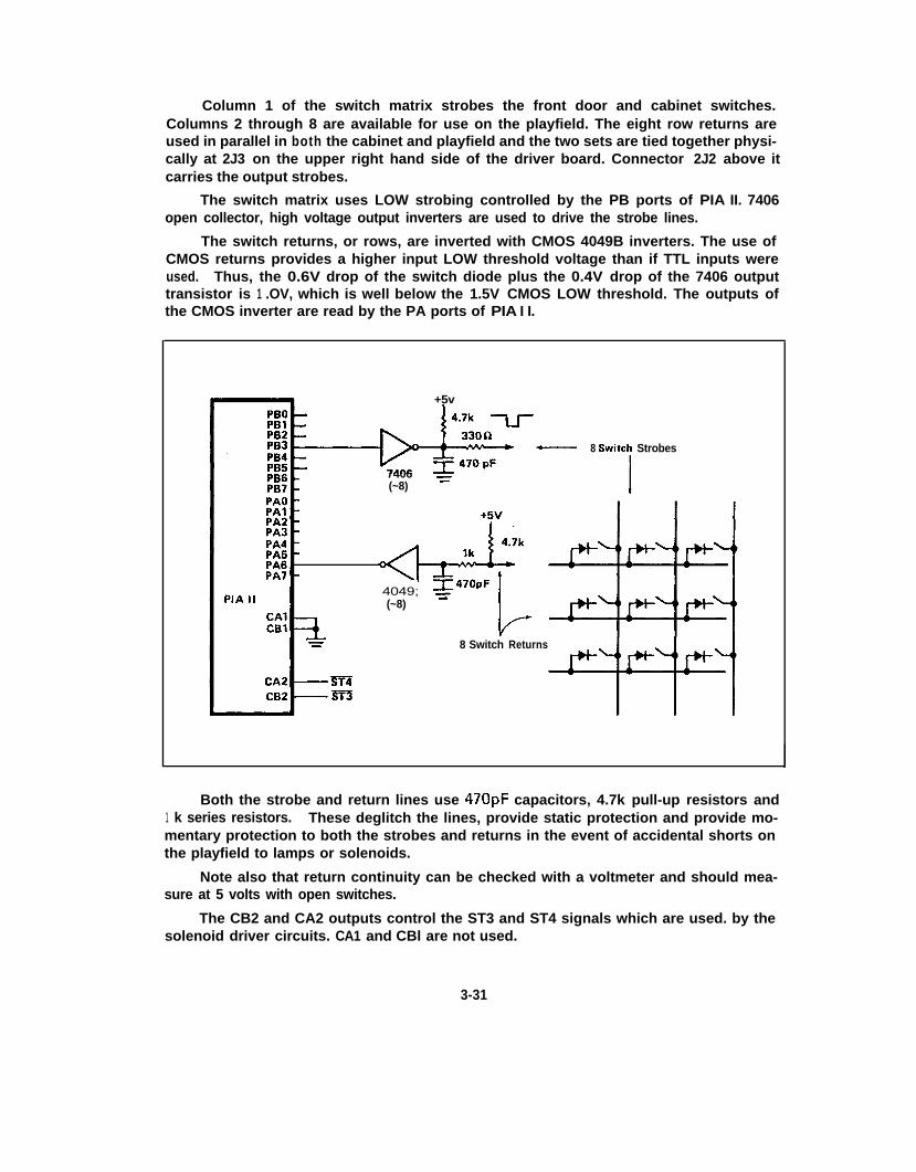
Column 1 of the switch matrix strobes the front door and cabinet switches.Columns 2 through 8 are available for use on the playfield. The eight row returns areused in parallel in both the cabinet and playfield and the two sets are tied together physi-cally at 2J3 on the upper right hand side of the driver board. Connector 2J2 above itcarries the output strobes.
The switch matrix uses LOW strobing controlled by the PB ports of PIA II. 7406open collector, high voltage output inverters are used to drive the strobe lines.
The switch returns, or rows, are inverted with CMOS 4049B inverters. The use ofCMOS returns provides a higher input LOW threshold voltage than if TTL inputs wereused. Thus, the 0.6V drop of the switch diode plus the 0.4V drop of the 7406 outputtransistor is 1 .OV, which is well below the 1.5V CMOS LOW threshold. The outputs ofthe CMOS inverter are read by the PA ports of PIA I I.
+5v
Lb*< -
7406 =(~8)
8 Switj Strobes
4049;(~8)
‘1=-ST4-?X3
8 Switch Returns
Both the strobe and return lines use 47OpF capacitors, 4.7k pull-up resistors and1 k series resistors. These deglitch the lines, provide static protection and provide mo-mentary protection to both the strobes and returns in the event of accidental shorts onthe playfield to lamps or solenoids.
Note also that return continuity can be checked with a voltmeter and should mea-sure at 5 volts with open switches.
The CB2 and CA2 outputs control the ST3 and ST4 signals which are used. by thesolenoid driver circuits. CA1 and CBl are not used.
3-31
A III Ports - The Lamp Matrix
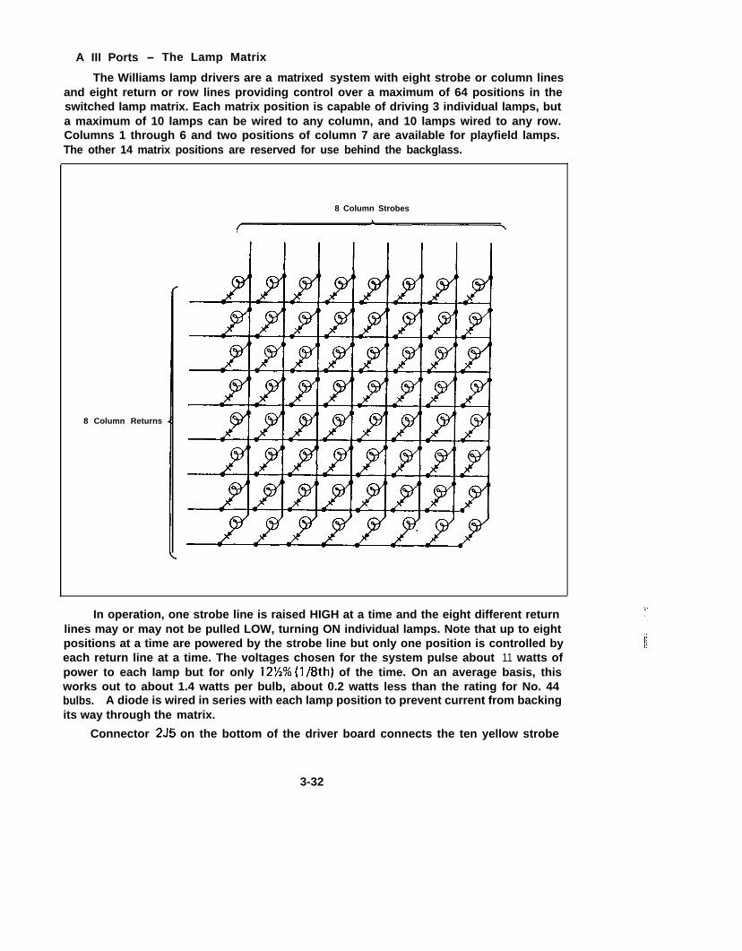
The Williams lamp drivers are a matrixed system with eight strobe or column linesand eight return or row lines providing control over a maximum of 64 positions in theswitched lamp matrix. Each matrix position is capable of driving 3 individual lamps, buta maximum of 10 lamps can be wired to any column, and 10 lamps wired to any row.Columns 1 through 6 and two positions of column 7 are available for playfield lamps.The other 14 matrix positions are reserved for use behind the backglass.
8 Column Returns 4
8 Column Strobes
In operation, one strobe line is raised HIGH at a time and the eight different returnlines may or may not be pulled LOW, turning ON individual lamps. Note that up to eightpositions at a time are powered by the strobe line but only one position is controlled byeach return line at a time. The voltages chosen for the system pulse about 11 watts ofpower to each lamp but for only 12X% (1/8th) of the time. On an average basis, thisworks out to about 1.4 watts per bulb, about 0.2 watts less than the rating for No. 44bulbs. A diode is wired in series with each lamp position to prevent current from backingits way through the matrix.
Connector 2J5 on the bottom of the driver board connects the ten yellow strobe
3-32
PIA III
PA0PA1PA2PA3PA4PA5PA6PA7
CA1CBl
CA2
CB2
-----
-255
+lBV1
1
Lamp Matrix Snobos(Columns)
Strobes (x8)
1
-VZ-ST-f
Matrix
Lamp hbtrix Returns(ROWS)
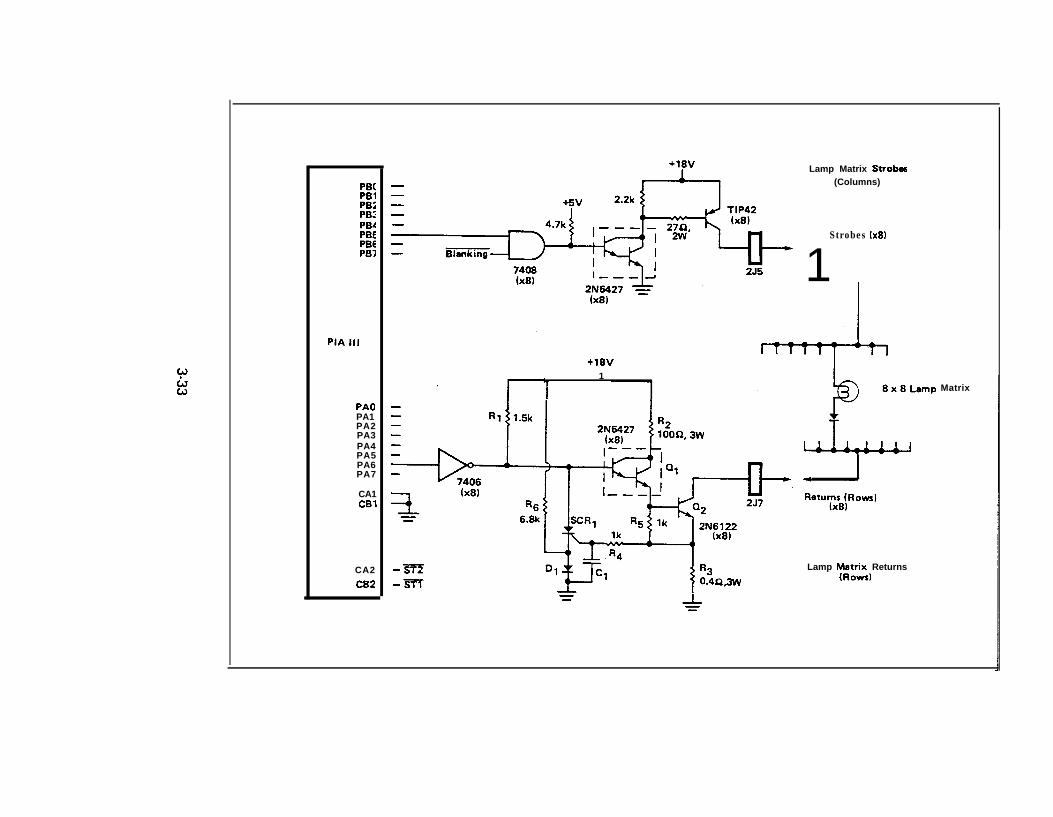
(column) lines to the playfield and insert board. Connector 2J7 connects the sixteen red‘urn (row) wires to the driver board.
The PB lines of PIA III, at IClO, control the eight identical column drivers. WhenLOW, the PB lines turn the strobe lines OFF. The Blanking signal from the CPU board isANDed by a 7408 AND gate with each PB output. When Blanking is LOW, all the lampsare OFF. The output of each AND gate controls a 2N6427 medium current NPNDarlington transistor. A 4.7k pull-up resistor provides the base current for the Darlington.
When the Darlington is ON, it provides base current via a 27R, 2 watt resistor to thetype TIP42 PNP high current driver transistor which turns fully ON, raising the strobeline to within 0.4V of the +18V lamp supply. When the PB output goes LOW, the outputof the AND gate’is LOW, the Darlington is OFF, and the 2.2k resistor helps keep thedriver turned fully OFF.
Also illustrated is one of the eight identical return or row drivers. The componentnumbers are different in the actual game. The row driver features a short circuitprotection built around an SCR.
The PA ports of PIA III control eight 7406 high voltage, open collector inverters.R1 is a pull-up resistor tied to the +18V supply and provides the base current for Ql, a2N6427 type Darlington when the output transistor of the inverter is OFF. When Ql isturned ON, it provides base current for Q2, the high current NPN row driver transistor,pulling the return line LOW, illuminating a lamp. R2 provides collector current for Ql.
The emitter voltage of Q2 is defined by Ohm’s Law and the current flowing throughR3. The driver only turns ON one lamp matrix position at a time and the current flow,assuming No.44 lamps, will be about 0.6A per lamp during each pulse. The voltage on R3will therefore be 0.4 x 0.6V = 0.24 volts/lamp. There is a 0.6 volt drop across each of thethree base-emitter junctions in this circuit, so the voltage at the base of Ql will therefore
0.24V + 2.4V = 2.64V. The voltage on the gate of SCR1 will be 0.24V by virtue of itsconnection to R3 via R4. 01 and R6 keep the cathode of SCR1 at 0.6V, meaning thatthe SCR will be in the OFF state during these conditions.
If a short in the matrix occurs, a large current will flow through R3, creating a largerthan normal voltage drop across it. If R3’s voltage reaches around 1.3V (over 3A), R4can supply enough gate current to SCR1 to switch it into its ON state. Cl deglitches thegate of SCR1. With the SCR ON, the base of Ql is clamped down to about 1.4 volts. R5helps pull the emitter voltage of Ql down to about 0.5 volts and turns Q2 fully OFF.
At the end of the ON pulse from the PA ports, the output transistor of the inverterpulls the anode of SCR1 down to 0.4V, which causes the SCR to switch immediatelyinto its OFF state. The next lamp column is then strobed and the row driver may or maynot be switched ON by the MPU.
If a short in a lamp, a socket, or the wiring does occur, only the lamp position withthe problem will be detected by the driving circuits; none of the other lamps in thematrix would be affected. Only a short duration (0.14psec) pulse will occur through theshort. No other circuit component would be affected.
PIA IV Ports - Solenoid Control
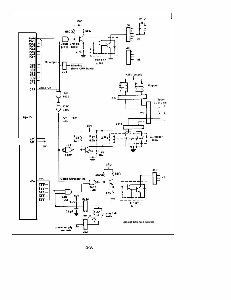
PIA IV is used to control 22 different solenoid driver transistors and a flipper relay.There are basically three circuit configurations. The first is the processor only controlled
3-34
drivers of which there are sixteen. The second is the flipper circuit and the third is thespecial solenoid drivers of which there are six.
The sixteen PA and PB ports of PIA IV are used as outputs to control the sixteenprocessor only controlled drivers. Each port output is first ANDed with the Blankingsignal with 7408 AND gates (ICl, IC2, IC3 and IC4). The port output must be HIGH toturn ON a coil. If the Blanking signal is pulled LOW, the solenoids are all OFF.
The outputs of the AND gates control a 2N4401 NPN buffer transistor. A 560 Rresistor provides base current for this transistor. Collector current for it is supplied bya 68Q resistor. When ON, the transistor provides the base current for a type TIP120 NPNDarlington driver transistor, turning it ON. The TIP120s provide the ground returns forthe ‘sixteen processor only controlled solenoids. Note that the driver ground is the sameas the logic ground. The 2.7k resistor helps keep the TIP120 turned fully OFF when it issupposed to be. Connectors 2J9 and 2Jll provide the connections to the coil returnwires.
The C82 output of.PIA IV is the Game On output signal to the rest of the drivers.When this line is HIGH, a game is in play. The Game On signal is ANDed with theBlanking signal with an AND gate of IC7. A 7402 NOR gate, IC9C, is wired as an inver-ter and connects to the output of this AND gate. Now, if either Game On or Blankinggoes LOW, the output of this NOR gate will ‘go HIGH, signalling the other seven driversto go OFF.
Another 7402 NOR gate, IC8A, inverts this signal again. When both Game On andBlanking are HIGH, the output turns Q13 ON which energizes flipper relay Zl. R25 pro-vides base current to Q13. R26 and R27 provide additional despiking control on therelay coil. In the event of failure of Dl, the additional loading helps prevent voltagespikes from the coil from entering the +5 volt supply.
When the relay is ON, the ground return circuits are completed to the flipper but-tons in the cabinet. If they are pressed, the flipper coils will energize.
The third set of solenoid drivers are the special solenoid drivers: The actual bufferand driver transistors and associated resistors are identical to the sixteen processor onlycontrolled drivers. The differences lie in the buffer circuits. The special solenoid driverscan be controlled by either the PIA ports or by playfield switches.
Six of the eight CA2 and CB2 ports of PlAs I through IV are used as special solenoidstrobe outputs and are called ST1 through ST6. These are normally HIGH but go LOWto turn ON one of these solenoids.
There are also six special switch inputs which have pull-up resistors on the driverboard but can be pulled LOW on the playfield by playfield switches and this also turnsON a coil. The 100R resistor and 22ccF, 15V capacitor are used to extend the length oftime that a coil is energized.
Both the STx lines and switch inputs are ANDed by a 7408 AND gate (IC6 andIC7). If either of the two input lines go LOW, the output will go LOW. The output isNORed with the Game On-Blanking output of IC9C by a 7402 NOR gate (IC8 and IC9).Both inputs must be LOW in order for there to be a H IGH output which turns ON a drivertransistor in the same manner as the processor only controlled solenoid drivers.
3-35
1+5V
J9
7400 2N4401-7(x16) (x161
2.7k
56on 166n‘
I
+
;--G=-l3 LEi
ImfJll
16 output
Game On
-ST5 --STl-STZ-
FE-ST6-
T I P 1 2 0 -s
Blanking(x161
(from CPU board)
+28V supply
flippers
IC77400
/ IC9C7402
8J3flipper
- b u t t o n s
7Jl
vt5v3.3k
=
t5v1
I - I
Special Solenoid Drivers
21 flipperrelay
J12
x6
3-36