the path toward efficient nano-mechanical circuits and systems
TRANSCRIPT

2nd Berkeley Symposium on Energy Efficient Electronic Systems
The Path Toward Efficient Nano-Mechanical Circuits
and Systemshttp://www.chi-yun.com/blog/wp-content/uploads/2008/10/ba-road-less.jp
Tsu-Jae King Liu1
Elad Alon1, Vladimir Stojanovic2, Dejan Markovic3
1University of California at Berkeley2Massachusetts Institute of Technology3University of California at Los Angeles
November 3, 2011
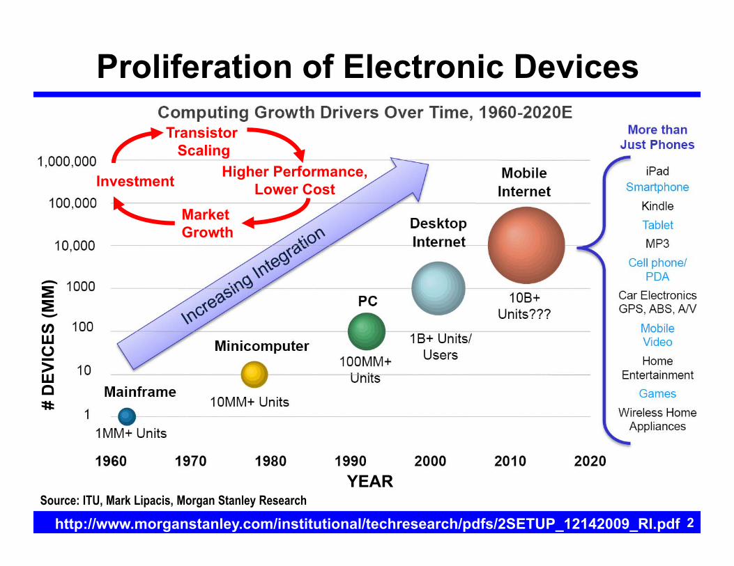
Source: ITU, Mark Lipacis, Morgan Stanley Research
http://www.morganstanley.com/institutional/techresearch/pdfs/2SETUP_12142009_RI.pdf
# D
EVIC
ES (M
M)
YEAR
Market Growth
Investment
Transistor Scaling
Higher Performance,Lower Cost
Proliferation of Electronic Devices
2

Infrastructionalcore
Sensory swarm(trillions of devices)
Vision for 2020: Swarms of Electronics
J. Rabaey, ASPDAC 2008 3
Driver for More of Moore’s Law
Driver for More Than Moore’s Law
Mobile access

Why Mechanical Switches?
• Relays have zero off-state leakage zero leakage energy
Source
DrainGate
Air gap
tgap tdimple
3-Terminal Switch
• Relays switch on/off abruptly allows for aggressive VDD scaling
(ultra-low dynamic energy)
1.E-14
1.E-12
1.E-10
1.E-08
1.E-06
1.E-04
Measured I-V
Gate Voltage
Dra
in C
urre
nt
S≈0.1mV/dec
VPIVRL
4

• Electro-Mechanical Relay Design for Digital ICs
• Relay-Based IC Design
• Relay Reliability
• Summary
Outline

• A voltage is applied between the gate and body to bring the channel into contact with the source and drain. Folded-flexure design relieves residual stress. Gate oxide layer insulates the channel from the gate.
4-Terminal Relay Structure
Body
Drain
Source
Body
Gate
Channel
A
A’
Isometric View:
Drain Source
Gate
Body
GateOxide
substrate
IDS
insulator
AA’ cross-section: OFF state
AA’ cross-section: ON state
6R. Nathanael et al., IEDM 2009

4-T Relay Process Flow (I)
100nm SiO2
80 nm Al2O3
50 nm W
Si substrate
200nm100nm
Deposit Al2O3 substrate insulator• ALD at 300oC
Deposit & pattern W electrodes• DC magnetron sputtering
Deposit 1st sacrificial LTO• LPCVD at 400oCDefine contact regions
Deposit 2nd sacrificial LTO
Deposit & pattern W channel
Deposit Al2O3 gate oxide
50 nm W
40 nm Al2O3
SiO2
Mask 1: Electrode
Mask 2: Contact dimple
Mask 3: Channel
7R. Nathanael et al., IEDM 2009

4-T Relay Process Flow (II)
8
TiO2
HFvapor
p+ poly-Si0.4Ge0.6
SiO2
1m
Deposit p+ poly-Si0.4Ge0.6 gate• LPCVD at 410oC
Coat with ultra-thin (~0.3nm) TiO2• ALD at 300oC
Pattern gate & gate oxide layers using LTO as a hard mask
Release in HF vapor
Mask 4: Structure
R. Nathanael et al., IEDM 2009
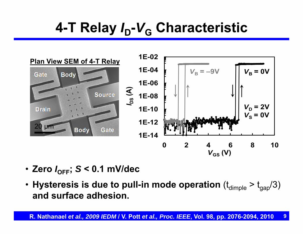
R. Nathanael et al., 2009 IEDM / V. Pott et al., Proc. IEEE, Vol. 98, pp. 2076-2094, 2010
4-T Relay ID-VG Characteristic
• Zero IOFF; S < 0.1 mV/dec• Hysteresis is due to pull-in mode operation (tdimple > tgap/3)
and surface adhesion.
Plan View SEM of 4-T Relay
20 μm
9
1E-14
1E-12
1E-10
1E-08
1E-06
1E-04
1E-02
0 2 4 6 8 10
I DS(A
)
VGS (V)
VD = 2VVS = 0V
VB = 0VVB = –9V
(a)

• Perfectly complementary operation is achieved in left and right channels
• VBL = 0 V; VBR = 10 V
Plan View Close-Up of Channel Region
See-Saw Relay Structure
Measured ID-VG Characteristics
1E-15
1E-13
1E-11
1E-09
1E-07
1E-05
1E-03
0 2 4 6 8 10
I DS
(A)
VG (V)
IDS_RIGHT
IDS_LEFT
VON_LEFT=VOFF_RIGHT=7.14V
VON_RIGHT=VOFF_LEFT=3.16V
LA=42μmLA1=12μmWA=40μm
J. Jeon et al., IEEE Electron Device Letters, Vol. 31, pp. 371-373, 2010 10

See-Saw Relay Latch
SRAM Cell VCTRL
VDATANMOS
G
DRDL
SRSL
BRBL
VSN
VWL
VBL
Seesaw
VDD
GND
NMOSStorage Node
Demonstrated SRAM Cell Operation
0
6
12
VW
L (V
)0
6
12
VD
ATA
(V)
0
6
12
0 5 10 15 20 25Time (s)
VB
L (V)
0
6
12V
CTR
L (V)
R = READW = WRITE (b-a)
(b-c)
(b-d)
W '0'
R '0' R '1' R '1'R '0'
W '0' W '1' W '1'
(b-b)
V DD=12V
11J. Jeon et al., IEEE/ASME J. MicroElectroMechanical Systems, Vol. 19, pp. 1012-1014, 2010.

4-T Relay Turn-On Delay
• Turn-on delay improves with gate overdrive, and saturates at ~200ns for VB = 0V.
Turn-ON Time vs. Gate Voltage Turn-ON Time vs. Body Bias
• Turn-on delay improves w/ body biasing to reduce VPI 100ns turn-on delay
12R. Nathanael et al., IEDM 2009
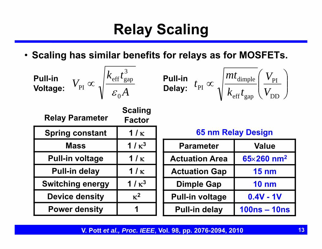
, , Relay Scaling• Scaling has similar benefits for relays as for MOSFETs.
65 nm Relay DesignSpring constant 1 / Mass 1 / 3
Pull-in voltage 1 / Pull-in delay 1 /
Switching energy 1 / 3
Device density 2
Power density 1
Relay ParameterScalingFactor
V. Pott et al., Proc. IEEE, Vol. 98, pp. 2076-2094, 2010
Pull-inVoltage:
Pull-inDelay:
Parameter ValueActuation Area 65260 nm2
Actuation Gap 15 nmDimple Gap 10 nm
Pull-in voltage 0.4V - 1VPull-in delay 100ns – 10ns
Atk
V0
3gapeff
PI
DD
PI
gapeff
dimplePI V
Vtk
mtt
13
• Electro-Mechanical Relay Design for Digital ICs
• Relay-Based IC Design
• Relay Reliability
• Summary
Outline

4 gate delays 1 mechanical delay
Digital IC Design with Relays
F. Chen et al., ICCAD 2008
• CMOS: delay is set by electrical time constant‒ Quadratic delay penalty for stacking devices Buffer & distribute logical/electrical effort over many stages
• Relays: delay is dominated by mechanical movement‒ Can stack ~100 devices before telec ≈ tmech
Implement relay logic as a single complex gate
15

Relay-Based VLSI Building Blocks
2010 ISSCC Jack Raper Award for Outstanding Technology Directions
F. Chen et al., ISSCC 2010 16
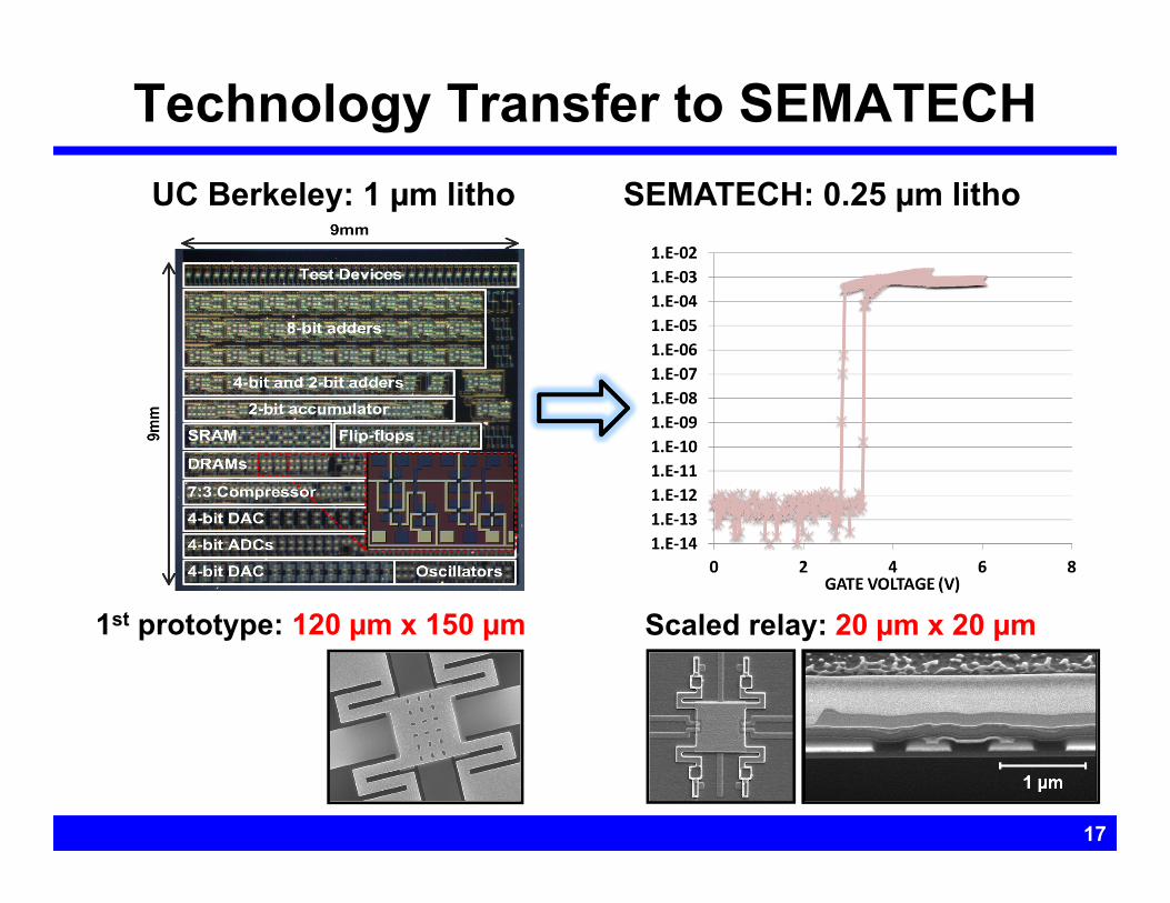
Technology Transfer to SEMATECH
1st prototype: 120 µm x 150 µm Scaled relay: 20 µm x 20 µm
SEMATECH: 0.25 µm lithoUC Berkeley: 1 µm litho
17
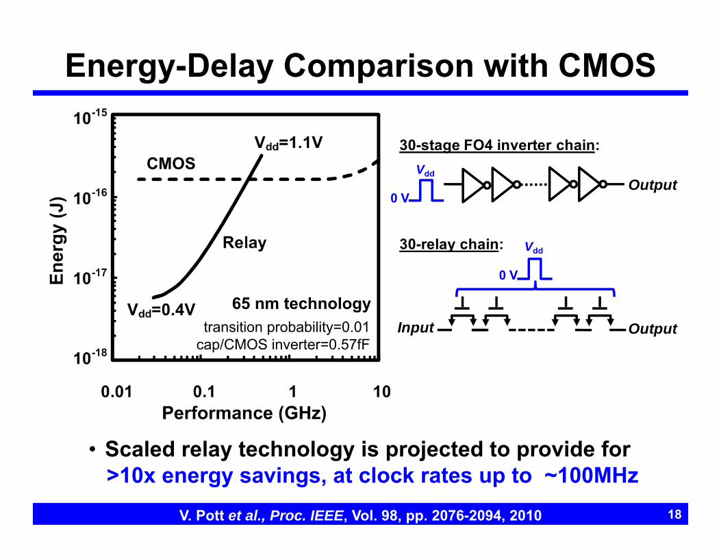
Energy-Delay Comparison with CMOS
transition probability=0.01cap/CMOS inverter=0.57fF
• Scaled relay technology is projected to provide for >10x energy savings, at clock rates up to ~100MHz
V. Pott et al., Proc. IEEE, Vol. 98, pp. 2076-2094, 2010 18
0 V
Vdd
OutputInput
30-stage FO4 inverter chain:
0 V
VddOutput
30-relay chain:
CMOS
65 nm technology
• Electro-Mechanical Relay Design for Digital ICs
• Relay-Based IC Design
• Relay Reliability
• Summary
Outline

• Hysteresis voltage (VPI-VRL) scales with the pull-in voltage (VPI)
• Surface adhesion force scales with area of contacting region(s):
ignoring surface adhesion force
Extracted from measured VPI,VRL
Stiction
H. Kam et al., 2009 IEDM 20
VGB
IDS
VPIVRL
Relay I-V

Contact Design for Logic Gates
• High RON (up to ~10 kΩ) is acceptable To achieve good endurance and reliability:
1. Use hard electrode material Tungsten2. Apply a surface coating to reduce surface force
and current density ALD TiO2
VDD
Electrical DelaytRC < 1 ps
Mechanical DelaytPI ~10 – 100 nsRON
21F. Chen et al., ICCAD 2008
CL

Contact Stability
• Variations are likely due to W oxidation• No surface wear is seen after 1 billion ON/OFF cycles
ON-state Resistance vs. # ON/OFF Cycles AFM Measurements
Never tested
Dimple
Rel
ativ
e di
strib
utio
n (a
. i.)
19nm
Dim
ple
(a) (b)
Rel
ativ
e di
strib
utio
n (a
. i.)
0 10 20 30 40 50
0 10 20 30 40 50
Height (nm)
Height (nm)
19nm
Dim
ple
(c) (d)
FRESH CONTACT
Contact Dimple
Rel
ativ
e di
strib
utio
n (a
. i.)
19nm
Dim
ple
Rel
ativ
e di
strib
utio
n (a
. i.)
0 10 20 30 40 50
0 10 20 30 40 50
Height (nm)
Height (nm)
Dim
ple
AFTER 109 cycles
Contact Dimple
3 μm
3 μm
19nm
1.E+02
1.E+03
1.E+04
1.E+05
1.E+06
1.E+0 1.E+3 1.E+6 1.E+9No. of on/off cycles
Con
tact
resi
stan
ce [Ω
]
100k specification
L=25m
Measured in ambient
H. Kam et al., IEDM 2009, R. Nathanael et al., IEDM 2009 22

Relay Endurance
• Endurance increases exponentially with decreasing VDD, and linearly with decreasing CL
• Endurance is projected to exceed 1015 cycles @ 1V
H. Kam et al., IEDM 2010 23

Nanoscale Relay Technology
• Sub-100 mV operation is possible‒ Zero IOFF enables VDD scaling without increasing leakage power‒ Hysteresis voltage scales with pull-in voltage
24
Node (nm) 15 11 8Actuation Gap (nm) 5.5 4 3Pull-in Voltage (mV) 113 100 86Release Voltage (mV) 73 66 58
* All dimensions scaled with technology node
Footprint for two switches = 14×14F2
Node (nm) 15 11 8Supply Voltage (V) 0.4 0.4 0.4Mechanical Delay (ns) 6.2 3.8 2.5
L. Hutin et al., to be published
Source1
Drain1
Source2
Drain2
Device Layout

Cross-Point Electro-Mechanical NVM Array
Smallest cell layout area (4F2); 3-D stackable Low-voltage operation Excellent retention behavior Multiple-time programmable (> 10,000 cycles)
25W. Kwon et al., to appear in IEEE Electron Device Letters
1E-13
1E-12
1E-11
1E-10
1E-09
1E-08
1E-07
1E-06
1E-05
1E-04
-1.5 -1 -0.5 0 0.5 1 1.5VBL[V]
|Cur
rent
| [A
]
Set stateReset state
• Electro-mechanical diode cell design:‒ Open circuit in Reset state‒ Diode in Set state (built-in electric-field electrostatic force)
Measured I-VCross-sectional SEMSEM of NVM Array

• Electro-Mechanical Relay Design for Digital ICs
• Relay-Based IC Design
• Relay Reliability
• Summary
Outline
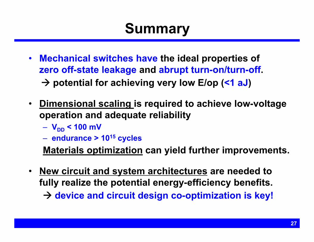
Summary
• Mechanical switches have the ideal properties of zero off-state leakage and abrupt turn-on/turn-off. potential for achieving very low E/op (<1 aJ)
• Dimensional scaling is required to achieve low-voltage operation and adequate reliability ‒ VDD < 100 mV‒ endurance > 1015 cyclesMaterials optimization can yield further improvements.
• New circuit and system architectures are needed to fully realize the potential energy-efficiency benefits. device and circuit design co-optimization is key!
27

Acknowledgements• NEM-Relay Team (current and former) members:
Post-docs: Louis Hutin; Hei Kam (now with Intel);Vincent Pott (now with IME, Singapore)
Students: Rhesa Nathanael, Jaeseok Jeon (now with Rutgers U.), I-Ru Chen, Yenhao Chen, Jack Yaung, Matt Spencer;Fred Chen and Hossein Fariborzi (MIT);Chengcheng Wang and Kevin Dwan (UCLA)
• Funding: DARPA/MTO NEMS Program DARPA/MARCO Focus Center Research Program
• Center for Circuits and Systems Solutions (C2S2)• Center for Materials, Structures, and Devices (MSD)
NSF Center of Integrated Nanomechanical Systems (COINS) NSF Center for Energy Efficient Electronics Science (E3S)
• UC Berkeley Micro/Nanofabrication Laboratory28

Frequently Asked Questions
1. Displacement (x) due to gravity?
2. Mechanical shock causing pull-in?‒ requires acceleration > 106g
due to small m (10-14 grams)
3. Thermal vibration? x ≈ 1Å for T = 300K
29
fm 1.0effk
mgx
2
21
21 xkTk effB