the ibm 1800 - gordon bellgordonbell.azurewebsites.net/.../chap33_ibm1800_cs1.pdf ·...
TRANSCRIPT

Chapter 33
The IBM 1800
Introduction
This third-generation computer is constructed with hybrid-circuit
technology (semiconductors bonded to ceramic substrates) known
as SLT (Solid Logic Technology). It has a core primary memory.The 1800 is designed for process control and real-time applica-
tions. It is nearly identical to the IBM 1130, which is designed
for small-scale, general-purpose, and scientific calculation appli-
cations. The two C's perform about the same for computation
bound problems. The 1130 and 1800 are not program compatible
with the "universal" IBM System/360 series, though introduced
at about the same time. However, the 1800 uses terminals and
secondary memories similar or identical to the System/360. These
are organized about the standard IBM System/360 8-bit byte. Thus
their common information media provide a link between the two.
Hence an 1800 is sometimes connected to the System/360 as a
preprocessor. The relative performance of the IBM 1130, 1800,
and the IBM System/360 can be seen on page 586. The 1800 has
a better cost/performance ratio than a System/360, Model 40 and
has the performance of a Model 30. From now on we will refer
only to the IBM 1800, although much applies to the IBM 1130.
The 1800's interface facilities include a large number of T's
which can connect to different physical processes; a multiple
priority interrupt facility with fast response; multiple Pio's which
can transfer information at high data rates;1 and a complete
instruction set for real-time, nonarithmetic processing.
We include the 1800 because it is a typical, 16-bit, real-time,
process control computer. The ISP is the most straightforward of
the IBM computers in the book (and perhaps the nicest). The
several different Pio's and their implementations are unusual and
should be carefully studied. Important aspects of the 1800 include
the PMS structure as it links to real-time processes, e.g., analog
processes; the straightforward Pc ISP (Appendix 1 of this chapter);
the specialized Pio's for real-time T's; the Pc implementation; and
the Pio implementation. The chapter is written to expose and
explain these aspects.2
By comparing the 1800 with Whirlwind, an evolutionary pro-
gression can be seen. Their ISP's are similar but, because of better
'Although we refer to the data channels as Pio's, they have a very limited
ISP for a Pio; in fact, they might better be called K's.
2 Some of the material in the chapter has been abstracted from the IBM1800 Functional Characteristics Manual.
technology, the 1800 shows an increase in capability. The 1800
Pc has a medium-sized state (ISP has six registers) including three
index registers. The implementation is not elegant; a single register
array and adder would provide the basis for a straightforward Pc
implementation. The 1800 has features which facilitate higher
information processing rates compared with Whirlwind. The major
change between Whirlwind and the 1800 machines was brought
about by the decreasing cost of registers and primary memory.In the 1800, all K's have independent memory (usually 1 — 2
words or characters) so that concurrent operation of almost all
the T and Ms via their K's is possible. In contrast, Whirlwind has
only a single, shared register in Pc, and only one device can
operate at a time.
Lower hardware costs allow multiple Pio's in the 1800. The
Pio's represent an unusual approach to information processing in
this period. The Pio's which process standard disk, magnetic tape,
and card reader are conventional, but the Pio's for analog and
process signals are novel and interesting. The latter Pio's are the
most unusual part of the 1800, and they allow independent pro-
grams in each Pio to do some very trivial processing tasks such
as alarm-condition monitoring independent of Pc. However, the
Pio's are limited; for example, it is difficult to transmit or receive
a data block between Ms and Mp (using a Pio) without surrounding
the data block with Pio control words (thereby transmitting the
control words).
The interrupt system is typical of second- and third-generation
computers and is comparable to the SDS 900 series (Chap. 42).
In later computers interrupt conditions are used to determine a
fixed address to which the processor interrupts. There are generally
many conditions (100 to 1,000), but only a few discrete levels (8
to 20). The 1800 depends on program polling within a discrete
interrupt level; each level has a unique, fixed address.
A principal ISP design problem is the addressing of the 65,536-
word Mp. Thus, a 16-bit number has to be generated within Pc
for an address. In this regard the 1800 behaves like the 12-bit
machines which have to address a 2 12(4,096) word memory, and
the modes or methods the 1800 uses for addressing are reasonable.
It should be noted that it is relatively difficult to write programs
which do not modify themselves. For example, the instruction,
Store Status, is changed by its execution.
399
400 Part 5 The PMS level Section 2 I Computers with one central processor and multiple input/output processors
A peculiar feature of the 1800 is its storage protection (see page
408). This feature should provide program relocation capability
in addition to protection, but it does not.
PMS structure
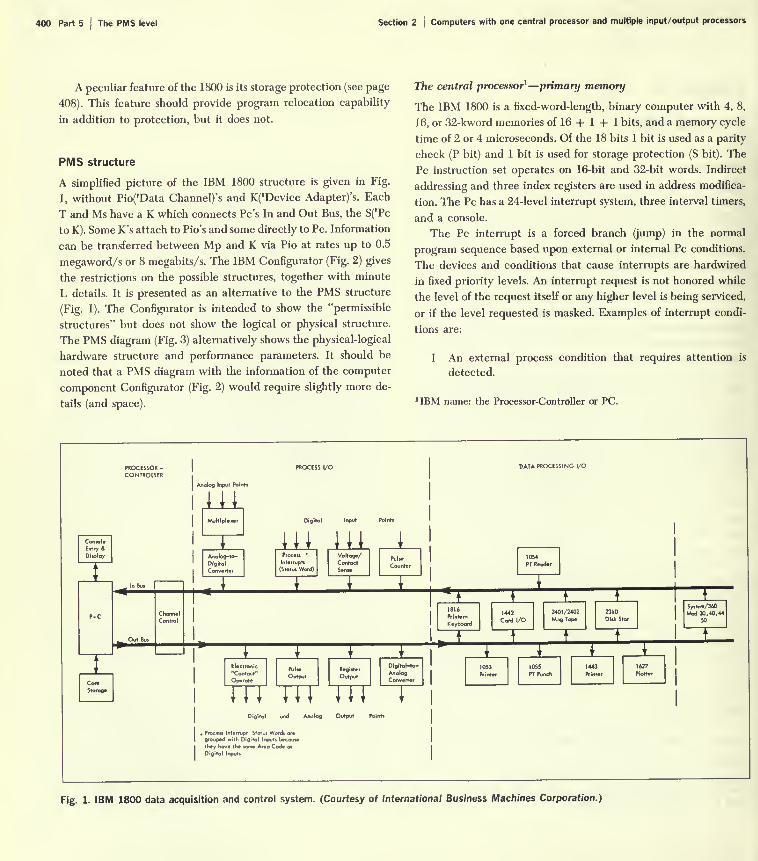
A simplified picture of the IBM 1800 structure is given in Fig.
1, without Pio('Data Channel's and K('Device Adapter's. Each
T and Ms have a K which connects Pc's In and Out Bus, the S('Pc
to K). Some K's attach to Pio's and some directly to Pc. Information
can be transferred between Mp and K via Pio at rates up to 0.5
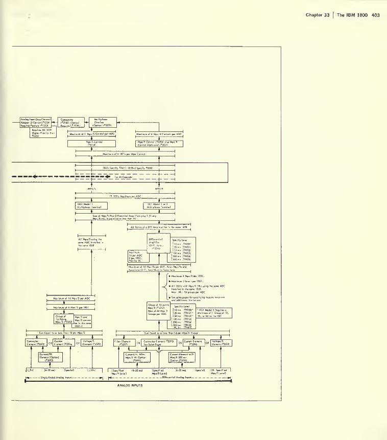
megaword/s or 8 megabits/s. The IBM Configurator (Fig. 2) gives
the restrictions on the possible structures, together with minute
L details. It is presented as an alternative to the PMS structure
(Fig. 1). The Configurator is intended to show the "permissible
structures" but does not show the logical or physical structure.
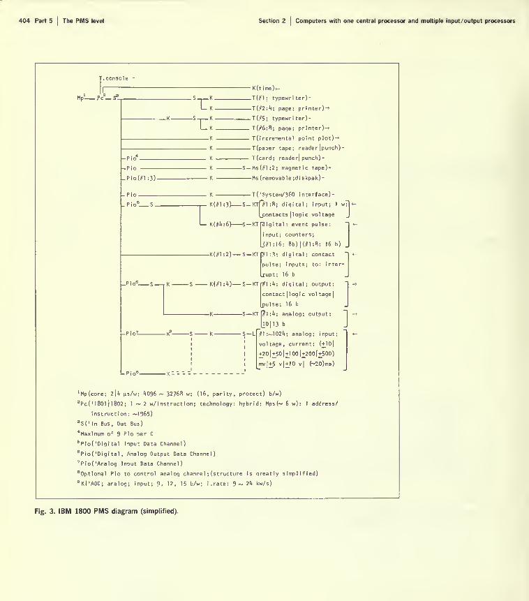
The PMS diagram (Fig. 3) alternatively shows the physical-logical
hardware structure and performance parameters. It should be
noted that a PMS diagram with the information of the computer
component Configurator (Fig. 2) would require slightly more de-
tails (and space).
The central processor1—
primary memory
The IBM 1800 is a fixed-word-length, binary computer with 4, 8,
16, or 32-kword memories of 16 + 1 + 1 bits, and a memory cycle
time of 2 or 4 microseconds. Of the 18 bits 1 bit is used as a parity
check (P bit) and 1 bit is used for storage protection (S bit). The
Pc instruction set operates on 16-bit and 32-bit words. Indirect
addressing and three index registers are used in address modifica-
tion. The Pc has a 24-level interrupt system, three interval timers,
and a console.
The Pc interrupt is a forced branch (jump) in the normal
program sequence based upon external or internal Pc conditions.
The devices and conditions that cause interrupts are hardwired
in fixed priority levels. An interrupt request is not honored while
the level of the request itself or any higher level is being serviced,
or if the level requested is masked. Examples of interrupt condi-
tions are:
1 An external process condition that requires attention is
detected.
JIBM name: the Processor-Controller or PC.
Entry &
ConStoroga
PROCESSOR -
COnfflcOUES
Channel
Analog Input Point)
HiInput Point
DATA PROCESSING I/O
LLi iliJAnolog-ro-

Chapter 33 The IBM 1800 401
MAGNETIC TAPE DISK STORAGE
DATA PROCESSING I/O
CARD I/OPAPER TAPE
S/360 ATTACHMENTI I
I S/ti.- 3*0
1/or 9 Track Haodt. "| |7 o> 5 Ttock M*o*.bp.ciM*9SS7) 0,1*9558) I | Sp*clV*9S57) or'*9558l|
»sf2 Drivoi per Syi*>
t, ,f .'-W« H*od) ('71251
23IO-A1, A2,«A3Moiimum on* 2310
CmSythtm/360 Chonn
iphu f*7720| Data Chonn* I

402 Part 5 The PMS level Section 2 Computers with one central processor and multiple input/output processors
.ADDITIONAL PRINTERS NO. 5 THROUGH 8 PRINTER AND PLOTTER
U4 3 Con he
('44371
E3JI44VIM7H Adopter ('4431'|
OPTIONAL FEATURES
• {'4709) Croup of 6 Additional Interrupt Unit - Max. 2 Group*' '
• ('3222) Additional Dots Channel (max: 6i•
• Up fo 4 Digital I/O Adoprtn in 1 BO I
B PIA Maximum per Syile
2 PIA per 1801 or 1876 Maximum
hqvilfl Cultomer Alignment (Form 170-1246)
Proceu Interrupt
Adopter (PIA)
('5710)
PI ( V) Group of
16»lri
('5716)
PI (C) Croup of
16Biti
('371a
ADC Mod 1 ('II
or ADC Mod 2
('1232) (MOa t—uim. DC
-J°^
Sum of DOC Plui 1856-1 Eql
I DOC per 1826 w I BO)
lion Voltooc Reference iPVx
1 ('35271 or Mod 2 ('53781
Digital OutputConrrol (DOC)
('329614 DAG Maximum pa. 1B36
Maximum 4 DOA in 1826
Maximum 2 DOA in 1801 .
Digital Output
Adapter (DOA)
C3295)
Maximum o(4 per DOA
jilol-Anoloa C<f4 (2ptl ('32
Buffer Regiiter
Single (»1507)1 per DAC (Opti<
BufU' RegkrerDouble ('15081
1 per DAC(OpHi
L~~i('361 2)
Pul.e Outputt
['58631
Regit ter Output16-Bit Regi.te.
1*61251
Pull* Output,
DIGITAL OUTPUTS^
PROCESS I/O
Analog Driver Amplifier
(ADA) Option ('12271
^5tAPA'. Option ('17271
1 r
ANALOG OUTPUTS
r
Chapter 33 The IBM 1800 403
Anolog InputOowChonnel'
Adopter 2 ''Option .'1234
»«^i'«iFiotm 1*12331
Require! DC Wit*
Higher Priority •(
*I233
Comparator('11851 (Option)
R.qui™(*1234)
MuitlplfO.
Overlap
(Option) t'S2S9l
t of 1 Mp./S Control per ADC 4 Mp. i- Contreli par ADC
I rV*>„/R Control l'5256> plut Mjw.lt
Control Additional ('52571
185h Specify '9477 1628-2 Specify »9090
MPX/S
-H 1
TMPX/K
11
404 Part 5 The PMS level Section 2 Computers with one central processor and multiple input/output processors
T. console -
Chapter 33 The IBM 1800 405
2 An interval timer has counted a previously set time interval.
3 A magnetic-tape drive has completed a data transfer previ-
ously requested and is ready for another request.
4 An operator has initiated an interrupt from the Pc console.
5 A device such as a typewriter has just printed a character
and is ready to receive the next one.
Primary-memory communication and data transmission with
terminals and secondary memory
Two methods are used to transmit data between Mp and Ms, or
Mp and T. First, low-speed devices are controlled directly by
the program. Each character or word of data is transmitted to or
from the Pc and onto T by means of an Execute I/0(XIO) instruc-
tion. The Pc program and device synchronization are accomplished
by using the interrupt mechanism. Devices operating under direct
program control include typewriter, printer, plotter, paper tape
(reader
and punch, analog-to-digital converters, contact sense,
voltage-level sense, pulse counters, etc.
The second method of transferring data is via the Pio('Data
Channel's. The Pio program is started by the XIO instruction of
the Pc. The transfer of data words then proceeds under control
(of
the specified Pio, completely asynchronous to and in parallel
with Pc program operation. The Pio gains Mp access independent
of Pc (Pc operation is suspended for one Mp cycle). During the
Mp cycle, the data are taken from or placed into core storage byPio (via internal Pc control and registers). As soon as the Pio has
been satisfied, which normally takes one cycle, the Pc proceeds.
The logical state of the Pc, or the Instruction-set Processor, is not
changed by Pio's access to Mp. This method of access is referred
to as "cycle stealing." Devices (Ms and T) operating under Pio
control include magnetic tapes, disks, line printer, card reader-
punch, and the link to the IBM System/360.
Some devices can operate under both Pc and Pio control,
depending on their characteristics and the configuration, e.g.,
analog input, analog output, digital input, and digital output.
Process I/O, controls and transducers
Analog inputs. Analog-input equipment includes analog-to-digital
converters, multiplexors, amplifiers, and signal conditioning equip-
ment to handle various analog-input signals. The data input rates
are up to 20,000 16-bit samples per second, with program selecta-
ble resolution and external synchronization. There can be 1,024
(via relay) and 256 (via high-speed solid state) multiplexed analog-
input channels connected to a single K (analog-to-digital con-
verter). The Configurator (Fig. 2) shows the allowable inputs.
Digital inputs. The Digital Input provides up to 384 process in-
terrupts; up to 1,024 bits of contact sense, digital input, or parallel
register input; and 128 bits of event input counters as 1-, 8-, and
16-bit counting registers.
Anatog outputs. Up to 128 analog outputs can be provided.
Digital outputs. Digital Outputs provide up to 2,048 bits of pulse
output, contacts, and registers.
IO processors (data channels)
Pio('Data Channels) give a T or Ms the ability to communicate
directly with Mp. For example, if an input unit requires a primary
memory cycle to store data that it has collected, the Pio communi-
cates directly with Mp and stores the data.
The Pio's run even if Pc is waiting. The Pio's have two registers:
a Word Count which is used to count the number of words beingtransferred in a block between a device and Mp memory; and a
Channel Address which points to the next word transferred in a
block. The Channel Address is also used to select the next instruc-
tion in the program for the next block transfer task.
Two basic types of Pio's are used, nonchaining and chaining.1
The Pio's provide the ability to transfer either a single block
(nonchaining) or multiple blocks (chaining) directly to Mp inde-
pendent of Pc.
The central processor
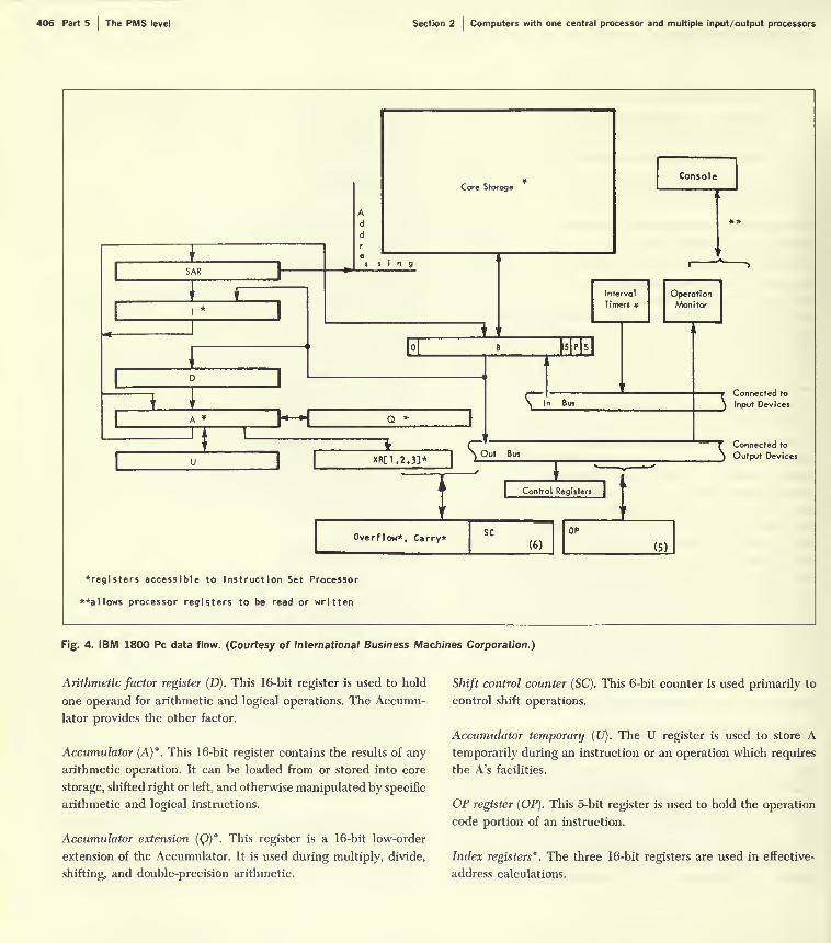
Registers in the physical processor
Figure 4 shows the relationship of the registers in Pc, together
with those in the Instruction-set Processor. Those registers acces-
sible by the program are shown with an °. All the registers are
accessible from the console. A description of the functions of each
register is given below.
Storage address register (SAR). All Pc references to Mp are selected
or accessed by this 16-bit register. Pio references to Mp use the
Channel Address Register (CAR) of the active Pio.
Instruction register (I)'. This 16-bit counter register holds the
address of the next instruction.
Storage buffer register (B). This 16-bit register is used for buffering
all word transfers with Mp.
1 A descriptive name undoubtedly concocted by one of IBM's marketing
departments.
406 Part 5 The PMS level Section 2 Computers with one central processor and multiple input/output processors
SAR
oA *
XJ C
] [ XR[ 1,2,3]*
Core Storage
Interval
Timers *
<5
EM
aOut Bui
IControl Registers
Overflow*. Carry*SC
(6)
OP
Console
OperationMon i tor
-r Connected to
\ Input Devices
"T Cor
\ Ounnected fro
tput Devices
(5)
registers accessible to Instruction Set Processor
**allows processor registers to be read or written
Fig. 4. IBM 1800 Pc data flow. (Courtesy of international Business Machines Corporation.)
Arithmetic factor register (D). This 16-bit register is used to hold
one operand for arithmetic and logical operations. The Accumu-
lator provides the other factor.
Accumulator (A)". This 16-bit register contains the results of anyarithmetic operation. It can be loaded from or stored into core
storage, shifted right or left, and otherwise manipulated by specific
arithmetic and logical instructions.
Accumulator extension (Q)°. This register is a 16-bit low-order
extension of the Accumulator. It is used during multiply, divide,
shifting, and double-precision arithmetic.
Shift control counter (SC). This 6-bit counter is used primarily to
control shift operations.
Accumulator temporary (17). The U register is used to store A
temporarily during an instruction or an operation which requires
the A's facilities.
OP register (OP). This 5-bit register is used to hold the operation
code portion of an instruction.
Index registers'. The three 16-bit registers are used in effective-
address calculations.
Chapter 33 The IBM 1800 407
Overflow and carry indicators' . The two indicator bits associated
with the Accumulator are Overflow and Carry. The Overflow
indicator can be turned on by Add, Subtract, or Divide instruction
and indicates a result larger than can be represented in the Accu-
mulator. The Overflow indicator can also be turned on by a Load-
status instruction. Once Overflow is on, it will not be changed
except by testing the indicator, or by a Load-status or Store-status
instruction. The Carry indicator provides the information that a
carry (or borrow) from the high-order position of the Accumula-
tor has occurred.
The Carry indicator is used with the Add, Subtract, Shift-left,
Load-status, Store-status, and Compare instructions.
In-bus. This 18-bit bus is a link(L) used to carry information from
a K to Pc. Generally only 16 of the 18 bits are used, although
transfers to magnetic tape can be made three 6-bit characters.
Out-bus. This 18-bit bus is used to carry information from Pc to
a K.
Instruction-set processor
The operation of the Pc from a program viewpoint follows. The
ISP registers were declared (*) in the previous section and in Fig.
4. The ISP registers are the 16-bit I, A, Q, XR [1, 2, 3], and the
1-bit Overflow and Carry.
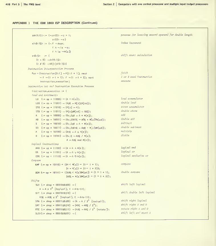
An ISP description of the 1800 appears in Appendix 1 of this
chapter. It is incomplete in the following respects: The memory
protect bit checking is not described; the illegal (undefined) in-
struction action is not described; double word data must be aligned
on even and odd address word boundaries or else a fault occurs;
and the IO instruction and interrupt operation are not given.
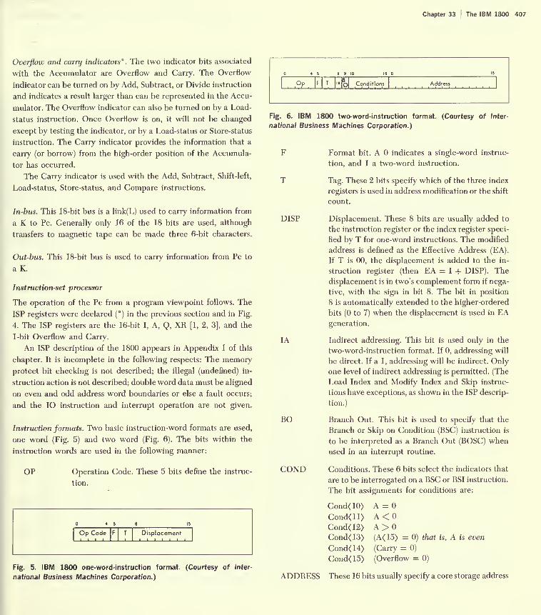
Instruction formats. Two basic instruction-word formats are used,
one word (Fig. 5) and two word (Fig. 6). The bits within the
instruction words are used in the following manner:
OP Operation Code. These 5 bits define the instruc-
tion.

408 Part 5 The PMS level Section 2 Computers with one central processor and multiple input/output processors
Table 1 Determining effective addresses
Chapter 33 The IBM 1800 409
contents of the I register are developed by one of the following
means, depending on the Pc operation:
1 The I register is incremented for each instruction.
2 The effective address of each instruction is developed in
the accumulator (A register) and then transferred to SAR.
The contents of the accumulator are saved in an auxiliary
(U) register during effective-address computation. If the
instruction was a branch, the contents of SAR is transferred
to the I register.
The following examples illustrate the data flow or instruction
interpretation process for the Load Accumulator (LD) instruction.
One-word load instruction
Instruction Cycle
1 A register transfers to U register.
2 I register transfers to SAR (I register is then incremented).
3 SAR addresses the memory location containing the instruc-
tion.
4 Memory location transfers to the B register and Out-bus.
5 Control registers store various parts of the instruction (op
code, format, and tag).
6 Displacement is stored in the D register.
7 a If tag = 00, I register transfers to A register.
b If tag =£ 00, the specified XR transfers to A register.
8 Displacement (D register) is added to A register.
Execute Cycle
9 A register transfers to SAR (effective address).
10 U register transfers to A register.
11 SAR addresses data word.
12 Data word transfers to B register.
13 B register loads into A register (via D register).
Two-word load instruction, direct addressingInstruction Cycle 1
1 A register transfers to U register.
2 I register transfers to SAR (I register is then incremented).
3 SAR addresses the memory location containing the instruc-
tion (first word).
4 Memory location transfers to B register and Out-bus.
5 Control registers store various parts of the instruction (op
code, format, and tag).
6 If tag t^ 00, the specified XR transfers to A register.
Instruction Cycle 2
7 I register transfers to SAR (I register is then incremented).
8 SAR addresses second word of instruction.
9 Second word of instruction (address) is read into B register.
10 Address (from B register) is stored in D register.
11 a If tag = 00, D register transfers to A register.
b If tag =^= 00, D register is added to A register (A register
contains contents of XR).
Execute Cycle
12 A register transfers to SAR (effective address).
13 U register transfers to A register.
14 SAR addresses memory at effective address (data word).
15 Data word transfers to B register.
16 B register loads into A register (through D register).
Central-processor communication with the controls 1
Direct program control of the controls
Pc direct programmed control of I/O devices is on the basis of
single-word or character-at-a-time transfers for each XIO instruc-
tion executed. One data word or character is transferred to or from
Mp to K. The XIO instruction specifies an I/O Control Command
(IOCC) with a function of Control, Sense, Read, or Write to a
controlled device. This command is either directly to a device or
to a Pio.
It is possible for the program sequence to execute an XIO
instruction to a device that is busy responding to a previous XIO
instruction. Each device has a Busy indicator, which signals
whether or not the device can accept data or control information.
(Incorrect program sequence timing may cause undetected errors.)
'IBM name: Adapter or Device Adapter.

410 Part 5 The PMS level Section 2 Computers with one central processor and multiple input/output processors
It is possible for a device operating synchronously with the 101
program to request a data word transfer before the program
sequence is ready to service the request. Devices with this poten-
tial have a "program check" indicator to signal when data have
been lost (that is, Pc has not kept up with the device). 110
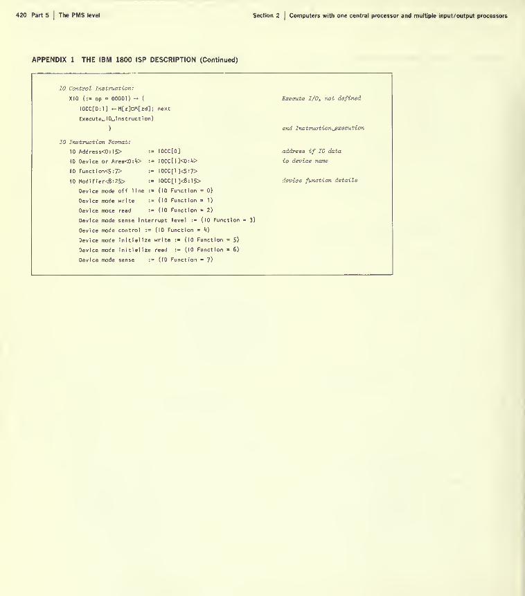
Execute I/O instruction (XIO)
This instruction is used for programmed I/O operations and to
initialize Pio; it may be either one or two words in length, as-qj
specified by the F bit. In the two-word instruction the address
is either a direct or indirect address, as specified by the IA bit.
For proper operation the effective address must be an even ad-
dress. The effective address is used to select a two-word I/O
Control Command (IOCC) from storage.
The IOCC specifies the I/O operation, I/O device, and core
storage address. The format of the two-word IOCC follows, with
an explanation of the assigned fields:
Initialize Write
Initiates a Write operation on a device or unit which
will subsequently make data transfers from storage via
a Pc.
Initialize Read
Initiates a Read operation from a device or unit which
will subsequently make data transfers to storage via a
Data Channel.
Sense Device
Reads the selected device status word into the Accu-
mulator. A Device Status Word (DSW) and the Process
Interrupt Status Word (PISW) are sensed with this
instruction.
If Area 00000 is specified, the Console status and
Interval Timer status may be brought into the Accu-
mulator as specified by a unit address code in the
Modifier field.
Area := IOCC[1](0:4) . The area field specifies a unique segment
of I/O which may be a single device (1442 Card Read-Punch, 1443
Printer, etc.) or a group of several units (magnetic-tape drives,
serial I/O units, contact sense units, etc.). (Area 00000 is used to
address system devices such as the console and the Interrupt Mask
Register.)
Function := !OCC[l](5:7). The primary I/O functions are speci-
fied by the 3-bit function code of the IOCC:
000 Removes an I/O device from on-line status and places
it in a "free" mode.
001 Write
Transfers a single word from storage to an I/O unit.
The address of the storage location is provided by the
Address field of the I/O Control Command.
010 Read
Transfers a single word from an I/O unit to storage.
The address of the storage location is provided by the
Address field of the I/O Control Command.
011 Sense Interrupt Level
Directs the selected I/O device to make its status
available in the Accumulator as the Interrupt Level
Status Word (ILSW).
100 Control
Causes the selected device to interpret the address
and/or Modifier of the IOCC as a specific control
action. Examples are feed card and load interrupt mask
register.
The current contents of the Accumulator are destroyed by the
execution of Sense Interrupt Level, Sense Device, Initialize Read,
Initialize Write, Read, or Write.
Modifier := IOCC[l}(8:15). This 8-bit field provides additional
detail for either Function or Area. For example, if the Area spe-
cifies a disk and if the Function specifies Control (100) then a
particular modifier code specifies the direction of the Seek opera-
tion. In this case, the Modifier serves to extend the function.
If, however, the Area specifies a group of I/O devices, and if
the Function specifies Write (001), then the particular unit address
is specified by the modifier.
Address : = IOCC[0](0:15) . The meaning prescribed for this 16-bit
field is dependent upon the Function specified by this I/O Control
Command:
1 If Function is Initialize Write (101) or Initialize Read (110),
then Address specifies the starting address of a table in
storage (an I/O block). The contents of this table are data
words and control information.
2 If Function is Control (100) and if, for example, Area speci-
fies the 1443 Printer, the Address may specify a specific
control action.
3 If Function is Sense (011 or 111), the Address field is ignored.
Instead, an increment of time equivalent to a memory cycle
is taken, during which the selected I/O device or Inter-
rupt Level places its status word in the accumulator.

Chapter 33 The IBM 1800 411
4 If Function is Write (001) or Read (010), the Address speci-
fies the storage location of the data word.
XIO execution interpretation process
1 The EA of the XIO is developed in the accumulator (A)
and routed to the Storage Address Register (SAR) to locate
the IOCC (as for any EA).
2 Rit position 15 of SAR is forced on to select the EA + 1
where the IOCC Area, Function, and Modifier are found.
3 The Area, Function, and Modifier are routed through the
R register to the Out-bus to the control of the device speci-
fied by the Area.
4 Rit position 15 of SAR is turned off to allow the address
portion of the IOCC word to be transferred from the Mplocation specified by the Effective Address (EA) to the R
register.
5 If the Function is an Initialize Read, Initialize Write, or
Control, the address part of the IOCC is routed throughthe R register to the Out-bus. The address part of the
Initialize Read/Write IOCC goes to the Channel Address
Register (CAR) of Pio. If the Function is Read or Write, the
address is routed from the R register through the A regis-
ter to the SAR. SAR addresses the memory location to or
from which the data are transmitted.
Interval timers
Three timers are provided to supply real-time information to the
program. They are in core-storage locations 0004 (Timer A), 0005
(Timer R), and 0006 (Timer C). Each timer is incremented ac-
cording to its associated or permanent time base and can be
hardwired to be 0.125, 0.250, 0.5, 1, 2, 4, 8, 16, 32, 64, or 128
milliseconds.
The timers can be started or stopped under program control.
When the count reaches zero, an interrupt is requested on the
level assigned to the timers.
Interrupt
The interrupt feature provides an automatic branch from the
normal program sequence, based upon an external condition. Amaximum of 24 external interrupt levels (groups) are available,
arranged in order of priority. Twelve external interrupt levels are
standard. Each interrupt level has a unique core-storage address
assigned to it. Several devices may be connected to a single inter-
rupt level, and program polling can be used to differentiate the
possible signals causing the interrupt. The Interrupt Level Status
Word, ILSW, is used to identify the specific condition causing its
interrupt level to request service.
Internal interrupt. When any one of the following error conditions
occur, there is an internal interrupt in Pc: an invalid op code;
a Mp parity error (an even number of bits); a storage-protect
violation; and Channel Address Register check error. The internal
interrupt takes priority over all external interrupts and cannot be
masked.
A mask register exists for the masking and unmasking of inter-
rupt levels. An interrupt level that is masked cannot initiate a
request for service until it has been unmasked.
Device status word (DSW). DSW indicators usually fall into three
general categories:
1 Error or exception interrupt conditions
2 Normal data or service-required interrupts
3 Routine status conditions
Process interrupt status word indicators (PISW). The PISW indi-
cators are physically located in Pc and are turned on by events
external to the computer, e.g., contact closures or voltage shifts.
10 processors1
The Pc initializes each Pio with an XIO instruction. The Pio has
priority to the extent that, when the I/O device is ready to send
or receive a data word, the Pc is stopped while the word transfers
to or from core storage. Pc data and conditions are undisturbed
except for the memory locations that receive data from an input
device.
I/O devices that are to be operated concurrently must be on
separate Pio's.
The XIO instruction for a Pio specifies an I/O Control Com-
mand (IOCC) with a function of Initialize Read or Initialize Write.
However, even though a device operates with a Pio, the XIO
instructions in Pc are used to sense device status and for control.
Registers
Channel address register. The Channel Address Register (CAR)is a 16-bit register used to store the Mp address of the next word
that will be addressed by the Pio. Each Pio has a CAR. Pio and
its associated CAR are selected when their assigned I/O device
is selected by the Area Code and Modifier of an IOCC word.
CAR is incremented by 1 after each transfer of its contents
to CAR.
^BM name: Data Channel (DC).

412 Part 5 The PMS level Section 2 Computers with one central processor and multiple input/output processors
Channel address buffer. A common Channel Address Buffer (CAB)
is used by all Channel Address Begisters to address Mp. When a
cycle steal request occurs, the CAB for the requesting Pio is
transferred into the Channel Address Buffer.
Channel-address-register check bit. Channel Address Begister
(CAB) checking is provided to ensure that the first word addressed
by a selected CAB is the first word of the correct data table. Thus
the check determines if a Pc program has set up the Pio program
correctly.1 A CAB check is made for all devices after the address
from the IOCC word is transferred to the selected CAB. A bit-
by-bit comparison is made between the contents of the selected
CAB and the contents of the B register. If any of the corresponding
bits are not equal, a CAB check error has occurred. This CABcheck error terminates the Pio task and initiates an internal inter-
rupt.
Word count register. A Word Count Begister is provided in each
Pio. The Word Count Begister is loaded with the contents of the
word-count portion of the data table, (2:15). This register is
decremented each time a data word is transferred from (to) the
data table.
Scan control register. A Scan Control Begister is provided in each
Pio that has chaining ability. Scan Control register bits are stored
in the first word of the first data table (bit positions and 1) and
in the second word (bit positions and 1) of the second data
table and all subsequent data tables in a chain.
The Scan Control Begister controls the I/O device and the Pio
operation at the end of the data table as follows: single scan of
data table and stop with an interrupt; single scan of data table
and stop (no interrupt); continuous scan of this data table or a
different data table with an interrupt at the end of this table; and
continuous scan of this data table or a different data table with
no interrupt.
The IO processor program operation
The sequence of steps for a Pio program is given below. The
memory map or format of the program is shown in Fig. 7.
1 Pc issues an XIO instruction which references the IOCCword and initializes Pio.
2 The Area Code and Modifier of the IOCC select the I/Odevice. Function specifies the type of operation (Initialize
Bead or Initialize Write, etc.).
1 Not a completely arbitrary program fault to check, since processors are in-
volved.
3 a The address portion of the IOCC word is stored in CABfor the selected Data Channel and I/O device.
b A CAB check is made between the selected CAB and
the B register.
4 A cycle steal is requested by Pio; CAB transfers to CAB.
5 CAB addresses core storage for the first word of the data
table while CAB is being incremented by 1.
6 The first word of the data table contains
a Scan Control bits (bit positions and 1)
b Word Count (bit position 2 to 15)
These are transferred to their respective registers in the I/Odevice. This is the end of the first cycle steal.
7 When another cycle-steal request from Pio occurs, CAB,which was incremented in step 5, now transfers the next
higher address to CAB. CAB then addresses core storagewhile CAB is being incremented.
8 The first data word is transferred to or from the I/O device
via the B register and Data Channel. The Word Count Beg-ister in the I/O device is decremented by 1. This is the
end of the second cycle-steal cycle.
Steps 7 and 8 now continue on a cycle-steal basis; that is, they
occur as the I/O device requests data transfers. The CAB is
incremented with each data transfer and the WCB is decremented.
This sequence continues until the last data word of the data table
is transferred. The last word transfer is sensed by the WCB reach-
ing zero or through some indicator in the device. If the device
does not have chaining ability, no more demands for data transfer
are made until the device is reinitialized with another XIO instruc-
tion.
Chaining. These steps are for the second and all subsequent data
tables. See above for steps 1 through 8.
9 The contents of the word following the last data word in
the first data table are transferred to CAB. This word must
contain the address of the next data table.
10 a When the next cycle is requested, CAB is transferred
to CAB to address core storage. The contents of the
first word of the next data table is transferred to the
B register. This word must contain the address of itself.
10 b CAB check is performed and CAB is incremented
by 1.
11 When the next cycle steal is requested, CAB is transferred
to CAB and CAB addresses Mp. The Scan-control bits and
Word-count bits are transferred from the second word of

Chapter 33 The IBM 1800 413
15 15
0000 1

414 Part 5 The PMS level Section 2|Computers with one central processor and multiple input/ output processors
S 1 2
L K
Chapter 33 The IBM 1800 415
Scan
ControlWord Count s m + 1
Initial Digital Input Group Address
Data 1
Data 2
Scan
ControlWord Count s n + 1
D or A Output Address
Data 1
Data 2
Data m Data n
Scan
ControlWord Count = 2m
Digital Input Group Addressj
Data 1
Digital Input Group Address2
Data 2
Scan Control Word Count = 2n
Initial D or A Output Address
Data;
D or A Output Address
Data2
Digital Input Group Address,,
Data m
D or A Output Addresses
Datai
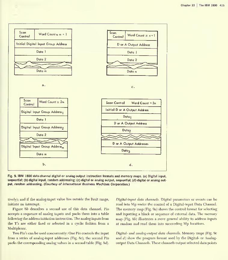
Fig. 9. IBM 1800 data-channel digital or analog-output instruction formats and memory maps, (a) Digital input,
sequential; (b) digital input, random addressing; (c) digital or analog output, sequential; (d) digital or analog out-
put, random addressing. (Courtesy of International Business Machines Corporation.)
tively); and if the analog-input value lies outside the limit range,
initiate an interrupt.
Figure 8fc describes a second use of this data channel. Pio
accepts a sequence of analog inputs and packs them into a table
following the address initiation instruction. The analog inputs from
the T's are either fixed or selected in a cyclic fashion from a
Multiplexor.
Two Pio's can be used concurrently: One Pio controls the input
from a series of analog-input addresses (Fig. 8c); the second Pio
packs the corresponding analog values in a second table (Fig. 8d).
Digital-input data channels. Digital parameters or events can be
read into Mp under the control of a Digital-input Data Channel.
The memory map (Fig. 9a) shows the control format for selecting
and inputting a block or sequence of external data. The memory
map (Fig. 9i>) illustrates a more general ability to address inputs
at random and read them into succeeding Mp locations.
Digital- and analog-output data channels. Memory maps (Fig. 9c
and d) show the program format used by the Digital- or Analog-
output Data Channels. These channels output selected data points

416 Part 5 The PMS level Section 2|Computers with one central processor and multiple input/output processors
to external analog or digital K's. This Pio is similar to the Digital-
input Data Channel.
Conclusions
We have tried to show a typical, third-generation computer used
for process control. Many of the facilities the 1800 possesses are
general. The Pio's are rather special, designed to monitor and
control a process, independent of Pc. Although the Pio's are
powerful (by providing parallel data transmission), their use, like
other multiprocessing systems, is nontrivial. The Pc ISP is fairly
straightforward, and one should write a program using it to ap-
preciate its simplicity.

Chapter 33 The IBM 1800 417
APPENDIX 1 THE IBM 1800 ISP DESCRIPTION
418 Part 5 The PMS level Section 2 Computers with one central processor and multiple input/output processors
APPENDIX 1 THE IBM 1800 ISP DESCRIPTION (Continued)
zd<0:15> := (-|Z<15> -»2 + 1;

APPENDIX 1 THE IBM 1800 ISP DESCRIPTION (Continued)
Chapter 33 The IBM 1800 419
(t = 0) -> (A ^A X 25
;C <-A<s-l>);
420 Part 5 The PMS level Section 2 Computers with one central processor and multiple input/output processors
APPENDIX 1 THE IBM 1800 ISP DESCRIPTION (Continued)
10 Control Instruction: