test and measurement challenges for 3d ic development
TRANSCRIPT
Test and Measurement Challenges for 3D IC Development
R. Robertazzi IBM Research

Page 2
Acknowledgements PFA
– Bill Price.– Pete Sorce.– John Ott.– David Abraham.– Pavan Samudrala
Digital Test– Kevin Stawaisz.
TEL P12 Prober– Glen Lansman, TEL USA.
Probing– Jerry Broz

Page 3
Outline Motivation For 3D Integration 3D Technology 3D Test in a Research Environment
– Instrumentation– Supporting Test at Different Stages in The Build – Probing Challenges– Probe Over Active for KGD Screen– Diced Chip Test
Conclusions

Page 4
Moore’s Law
1900 1910 1920 1930 1940 1950 1960 1970 1980 1990 2000 2010 2020
Historically, IC performance improvements have depended on scaling planar device structures.
3D 2D 3D

Page 5
Why 3D? Scaling of transistors and other
circuit elements is becoming more difficult.– Approaching fundamental physical
limitations on device size. Interconnect latency is beginning
to limit IC performance.– Vertical connections allow shorter
connections (50 m vs. 10 mm).– Expansion of numbers of
interconnects through compact vertical connections.
Easier to include disparate technologies.– Logic, EDRAM, opto‐electronics, non‐
silicon based…
!

Page 6
Challenges For 3D Integrated Circuits
Design– Timing analysis, clocking.– DFT.
Process– Functionality / yield at single stratum.– Characterization of 3D building blocks (TSV, bonding process).
Test– Definition of test points: Where and what to set, KGD strategy.
– How to test, probing.

Page 7
3D Technology Test Site
Face to back stacking scheme. Cu TSV on small pitch, C4
inter‐strata interconnect. Package pitch Std C4 for
package interconnect and final SP layer probing.
Thin
Small
Std Pitch
TSV
C4
Std. C4
SPSNS0
Stacked Chip Nomenclature
Page 8
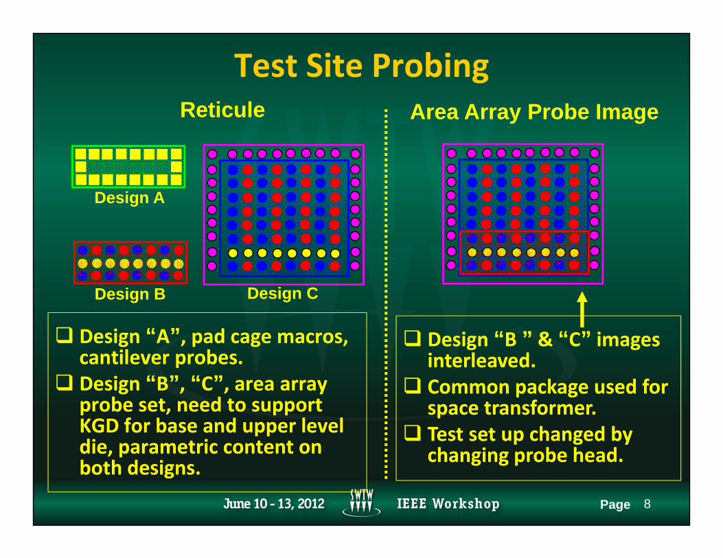
Test Site Probing
Design “A”, pad cage macros, cantilever probes.
Design “B”, “C”, area array probe set, need to support KGD for base and upper level die, parametric content on both designs.
Reticule
Design A
Design B Design C
Area Array Probe Image
Design “B ” & “C” images interleaved.
Common package used for space transformer.
Test set up changed by changing probe head.

Page 9
3D Process Characterization
3D process characterization requires measuring resistances from 1m Y 1G (>12 orders of magnitude).
True 4 point SMUs will be required to cover the low impedance range.
Resistive -C4
Bridge FaultOpen TSV
Leaky TSV
TSV Failure Modes -C4 Failure Modes

Page 10
Interfacing To The Probe Card
Cable‐to‐board signal modules
Clock / 3 GHz Ports Parametric– Agilent 34980A interface for
2&4 point resistance measurements, leakage.
Modular Probe Interface
Parametric
High Speed
Std I/O

Page 11
Test Points During Build(Probe Options & Risk Assessment )
Build Level VLSI Technology DUT
SP (Thick)
SP (Thin)
SN
Assembled, pre-packagedAssembled, packaged
No loss of yield observed PFA in progress
Assumed OK
Cantilever probes
Pointed vertical, probe over active
Flat vertical, chip tray

Page 12
Single Stratum Probing Options Single stratum test required:
– Design verification.– Known good die (KGD) prior to 3D
stacking. Current injection over full area
of the chip for cache. Major issues for area array
probing for single layer:– No qualified probe technology for
fine pitch uC4 probing.
Drives choice to area array probe card, pointed probes contacting Al TD landing pads.
Areas of concern:– Pad placement, where to probe.– Damage introduced through
probing process.
Probe Pad
Power Grid
Al Pad Probing, Pointed Probes
Option #2
C4 Cluster Probing, Flat Probes
Option #1

Page 13
Probing / Damage Experiments: Test Vehicle Top level film stacks similar to
3D test chips. Area array probe card used
with 4/9 image.– ~ 100 Power/ground contacts
measured in parallel for leakage.– ~ 40 signal contacts measured
individually.– ~ 100 sites probed/die.
Contactor– 5 mil Palinaey‐7 probe.– Probe tip diameter 10 m – Overdrive 0‐160 m (0‐6.5 mils).
Electrical leakage and SEM cross‐sections evaluated after probing.
Probe Image
Electrical Set UpPG Set Signal Set
Test Vehicle

Page 14
Probing / Damage Experiments: Test Vehicle Top Layer Dielectric Investigations
Stack “A” dielectric fails at first probe contact. Stack “A” + “B” dielectric fails after 120 m – 170 m overdrive.
-80 -60 -40 -20 0 20 40 60 80 100 120 140 160 1801E-12
1E-11
1E-10
1E-9
1E-8
1E-7
1E-6
1E-5
1E-4
1E-3
0.01
0.1
1
0
5
10
15
20
25
30
35
40
1000 Å"A"
Max
imum
Num
ber o
f Sig
nal P
ins
Mak
ing
Con
tact
Max
imum
Pow
er /
Gro
und
Leak
age
(A)
Overdrive From 50% Contact Point (m)
P/G Pins, Leakage
First Fail
Cu
Dielectric "A"100 Sites ~10,000 Touchdowns1 Volt
Au Reference Plate S/G Pins, Punch Thru
-80 -60 -40 -20 0 20 40 60 80 100 120 140 160 1801E-12
1E-11
1E-10
1E-9
1E-8
1E-7
1E-6
1E-5
1E-4
1E-3
0.01
0.1
1
0
5
10
15
20
25
30
35
40
2000 Å "B"1000 Å "A"
Max
imum
Num
ber o
f Sig
nal P
ins
Mak
ing
Con
tact
Max
imum
Pow
er /
Gro
und
Leak
age
(A)
Overdrive From 50% Contact Point (m)
P/G Pins, Leakage
First Fail Cu
Dielectric "A" + "B"100 Sites ~10,000 Touchdowns1 Volt
Au Reference Plate S/G Pins, Punch Thru

Page 15
Probe Scratch Test
Stack “A” dielectric fails with minimal probe scrub.
Stack “A”+“B” fails at moderate probe force.
Stack “A”+“B” +”C” shows no visual signs of failure, even with application of high probe force.Dielectric “A” + “B”
Dielectric “A” Dielectric “A” + “B” + ”C”

Page 16
Probing / Damage Experiments: Test Vehicle Full Pad Stack
Experiments done with and without Al pad layer. No fails observed for 10,000 probe/pad touchdowns. No observations of cracking from cross‐sections*.
Electrical Leakage Film Stack Damage Assessment
-80 -60 -40 -20 0 20 40 60 80 100 120 140 160 1801E-12
1E-11
1E-10
1E-9
1E-8
1E-7
1E-6
1E-5
1E-4
1E-3
0.01
0.1
1
0
5
10
15
20
25
30
35
40
6500 Å"C"2000 Å"B"1000 Å"A"
Num
ber o
f Sig
nal P
ins
Mak
ing
Con
tact
Max
imum
Pow
er G
roun
d Le
akag
e (A
)
Overdrive From 50% Contact Point (m)
P/G Pins, Leakage
All Pass
Bare or Al Pad
Dielectric "A"+"B"+"C"100 Sites ~10,000 Touchdowns1 Volt
Cu
Au Reference Plate S/G Pins, Punch Thru
*N. B. J. Yorita, SWT 2004 !

Page 17
3D Test Site Probe Pads
Sn: No C4 on probe pad, full pad available for probing.
Sp: Std. C4 on each probe pad, probing zone offset from contact via / C4 attachment zone.
3 mil probes.
SP, SN
Via
Al Pad
SP Probing Area 90
130
S0 Pad
SP Pad
AlCu
Dielectric

Page 18
Top Down SEM on Pads
Sequential etch of top pad metallization.1. Al/Cu/Dielectric.2. Cu/Dielectric.3. Adhesion Layer/Dielectric. Top down SEM reveals some disturbance of interfacial region.
1. Al Probe Mark
2. Cu
3. Interface

Page 19
AFM On Probe Marks
AFM reveals 30 nm depression in top adhesion layer.
= 31 nm

Page 20
TEM Cross Sections on Probed Pads
No evidence of damage or crack propagation in top insulating layer stack.
Pad
Interface Layer
Insulator Stack
3 m
200 nm

Page 21
Screen Yield, Design “B”, Using Probe Over Active
Wafer screen data shows no increased yield fallout over standard C4 probing using pointed probe over active probing strategy.
-5 0 5
-4
-3
-2
-1
0
1
2
3
4 F
F
F
F
F
F
F
F
F
F
S0 wafer SOC3
F
F
F
F
F
-1
0.1
1.2
2.3
3.4
4.5
5.6
6.69
7.8
8.9
10
IDD
Q (A
)

Page 22
In the research environment, we employed a chip to chip bonding strategy for 3D IC assembly.
Supporting single die test of complex area array chips has always been problematic:– Vision systems in advanced probers not
designed to work with single die efficiently.
– Chip transfer to chuck requires attachment to handler wafer, with adhesive.
3D chip bonding process development greatly benefits from pre‐packaged test:– Does the chip work, is it worth
packaging?– Does the packaging process affect chip
yield?– What does the chip look like visually after
test?
Diced Chip TestDouble Layer, 3D Chip
SpS0

Page 23
TEL custom build chip tray for diced chip designs “B” &”C”.
Clean, vacuum hold down technology which works with standard “Table Load” P12 wafer transfer procedure.
Two piece design allows easily changing to another chip size, requires only replacing top guide.
Alignment marks included for automated load, alignment and wafer scan.
Diced Chip TrayChip Tray
Design “B”

Page 24
Thermal resistance (RT) measurements for chips in tray show resistance RT ~4.6 x higher than measured with full wafer in contact with a Cu chuck.
For VLSI designs “B” &”C”, no problem encountered in running low speed functional screen tests, or performance tests for brief periods.
Chip Tray Thermal Resistance
0 2 4 6 8 10 12 14 1624
26
28
30
32
34
36
38
40
TChuck = 25oC
RT(Chuck) = 0.56 oC/W
Chi
p Te
mpe
ratu
re (o C
)
Chip Power (W)
RT(Tray) = 2.6 oC/W
Tray
Chuck

Page 25
Conclusions
3D introduces a number of new challenges in chip test, probing in particular.
A hierarchical test strategy has proven essential in 3D bonding process development learning.– Accessibility of test at all points in the build.– Access to on‐board parametrics.– Ability to test diced, bonded chips, pre‐packaged.
Fine pitch vertical probe/prober technology required to support current and future 3D fabrication technologies.