technology and manufacturing day - intel · pdf filetechnology and manufacturing day ......
TRANSCRIPT

TECHNOLOGY AND MANUFACTURING DAY
STACY J. SMITHGROUP PRESIDENT, MANUFACTURING, OPERATIONS AND SALESSEPTEMBER 19, 2017
Strategy overview

TECHNOLOGY AND MANUFACTURING DAY
Legal DisclaimerDISCLOSURES
China Tech and Manufacturing Day 2017 occurs during Intel’s “Quiet Period,” before Intel announces its 2017 third quarter financial and operating results. Therefore, presenters will not be addressing third quarter information during this year’s program.
Statements in this presentation that refer to forecasts, future plans and expectations are forward-looking statements that involve a number of risks and uncertainties. Words such as “anticipates,” “expects,” “intends,” “goals,” “plans,” “believes,” “seeks,” “estimates,” “continues,” “may,” “will,” “would,” “should,” “could,” and variations of such words and similar expressions are intended to identify such forward-looking statements. Statements that refer to or are based on projections, uncertain events or assumptions also identify forward-looking statements. Such statements are based on management’s expectations as of September 19-20, 2017, and involve many risks and uncertainties that could cause actual results to differ materially from those expressed or implied in these forward-looking statements. Important factors that could cause actual results to differ materially from the company’s expectations are set forth in Intel’s earnings release dated July 27, 2017, which is included as an exhibit to Intel’s Form 8-K furnished to the SEC on such date. Additional information regarding these and other factors that could affect Intel’s results is included in Intel’s SEC filings, including the company’s most recent reports on Forms 10-K, 10-Q and 8-K reports may be obtained by visiting our Investor Relations website at www.intc.com or the SEC’s website at www.sec.gov.

TECHNOLOGY AND MANUFACTURING DAY

TECHNOLOGY AND MANUFACTURING DAY
Two Implications:
1. Cost per square millimeter goes up over time
2. Doubling of transistors = “Scaling” Improves performance
Cost per transistor declines
“The number of transistors and resistors on a chip doubles every 24 months”
-Gordon Moore

TECHNOLOGY AND MANUFACTURING DAY
What if Moore’s Law is applied to…Terracotta Warriors ?
We could build 64 billion warrior statues
Agricultural productivity?
We could feed the world’s population with 1km2 of land
Transportation?
We could travel to the Sun on a single gallon
Source: Intel Internal Analysis.

TECHNOLOGY AND MANUFACTURING DAY
Is Moore’s Law dead?

TECHNOLOGY AND MANUFACTURING DAY
Is moore’s law dead? NO!mm2 / Transistor
(log scale)
13
0 n
m
90
nm
65
nm
45
nm
32
nm
22
nm
14
nm
10
nm
7 n
m
$ / mm2
(log scale)
13
0 n
m
90
nm
65
nm
45
nm
32
nm
22
nm
14
nm
10
nm
7 n
m
13
0 n
m
90
nm
65
nm
45
nm
32
nm
22
nm
14
nm
10
nm
7 n
m
$ / Transistor(log scale)
Source: Intel

TECHNOLOGY AND MANUFACTURING DAY
The time between nodes has lengthened…
Are you Getting the same Moore’s Law benefit?

TECHNOLOGY AND MANUFACTURING DAY
YES!Because we are getting
more scaling

TECHNOLOGY AND MANUFACTURING DAY
We Are Hyper Scaling(on 14 nm & 10 nm)
Hyper scaling enables us to achieve accelerated density improvement
Intra-node optimizations enable an annual cadence of product enhancements

TECHNOLOGY AND MANUFACTURING DAY
Microprocessor die area scaling
Hyper scaling delivers better than 0.50x die area scaling on 14 nm and 10 nm
100 mm2
45 nm 32 nm 22 nm 14 nm 10 nm
62 mm2
17.7 mm2
7.6 mm2
0.62x
Logic
SRAM
IO
100 mm2
Logic
SRAM
IO
100 mm2
Logic
SRAM
IO
100 mm2
Logic
SRAM
IO
100 mm2
Logic
SRAM
IO
0.43x
0.46x
0.62xArea
38.4 mm2
Source: Intel

TECHNOLOGY AND MANUFACTURING DAY
Moore’s Law Translates to Lower Product Costs22 nm & 14 nm Client Cost Curves
(Launch + 5 quarters)
Q2'12 Q2'13 Q2'14 Q2'15 Q2'16 Q2'17
$
0
Broadwell
SkylakeHaswell
Ivybridge
Kabylake
Source: Intel

TECHNOLOGY AND MANUFACTURING DAY
Moore's Law in action…PC CPU Weighted Average Cost Per Transistor ($/MTX)
(log scale normalized to 90nm)
Source: Intel
Q2'04 Q2'05 Q2'06 Q2'07 Q2'08 Q2'09 Q2'10 Q2'11 Q2'12 Q2'13 Q2'14 Q2'15 Q2'16 Q2'17
$/MTX
90nm
65nm45nm
32nm22nm
14nm

TECHNOLOGY AND MANUFACTURING DAY
Gross MarginsGross Margin % Annual 2005 – 2017F
2016 and 2017 forecasted figures are on a non-GAAP basis. Refer to Intel’s earnings release for a reconciliation of these non-GAAP measures at www.intc.com. 2017 forecasts are Intel estimates, based upon current expectations and available information and are subject to change without notice.Source: Intel
40%
45%
50%
55%
60%
65%
70%
2005 2006 2007 2008 2009 2010 2011 2012 2013 2014 2015 2016 2017F

TECHNOLOGY AND MANUFACTURING DAY
Competitors are announcing10nm this year…
Have you lost your lead?

TECHNOLOGY AND MANUFACTURING DAY
14nm Is ~3 years ahead
0.1
1
0.01
LO
GIC
AR
EA
(re
lati
ve
)
HVM WAFER START DATE
2007 2008 2009 2010 2011 2012 2013 2014 2015 2016 2017 2018 2019 2020
45nm
32nm
22nm
14nm
10nm
Intel
40/45nm
28nm
20nm
14/16nm
10nm
Others
3 years
Source: Intel

TECHNOLOGY AND MANUFACTURING DAY
Our Scale

TECHNOLOGY AND MANUFACTURING DAY
Investment Required to Build & EquipA Leading Edge Wafer Factory
~$10b

TECHNOLOGY AND MANUFACTURING DAY
Si technology is becoming rare
Other names and brands may be claimed as the property of others.
Note: GF relies on Samsung’s process recipe for 14nm. GF-IBM Fabsacquisition announced in 2014
Source: Analyst reports; company information
02-'03 04-'06 06-'08 08-'12 10-'12 12-'14 14-'16
NUMBER OF PLAYERS WITH A LEADING EDGE LOGIC FAB25
18
13 13
8
5
TSMCIntel
SamsungGF
IBMST-MUMC
Panasonic
TSMCIntel
SamsungGF
IBM
(130nm) (90nm) (65nm) (45/40nm) (32/28nm) (22/20nm)
TSMCIntel
SamsungAMDIBM
ST-MUMC
PanasonicFujitsu
RenesasSMIC
Freescale
InfineonSony
CypressSharp
ADIAtmelHitachi
ONRohmSanyo
Mitsubishi
TIToshiba
TSMCIntel
SamsungAMDIBM
ST-MUMC
PanasonicFujitsu
RenesasSMIC
Freescale
InfineonSony
CypressSharp
TIToshiba
TSMCIntel
SamsungGF
IBMST-MUMC
PanasonicFujitsu
RenesasSMIC
TIToshiba
(16/14nm)
4
TSMCIntel
SamsungGF
TSMCIntel
SamsungGF
IBMST-MUMC
PanasonicFujitsu
RenesasSMIC
TIToshiba

TECHNOLOGY AND MANUFACTURING DAY
Fab and Assembly Test Sites
Wafer FabsAssembly Test
IrelandOregon
Arizona
ChengduVietnam
PenangKulim
DalianIsraelNew Mexico

TECHNOLOGY AND MANUFACTURING DAY
Global Manufacturing By the Numbers
28
INTEL EMPLOYEES MANUFACTURING SPACE TRANSISTORS
~30K +4MSQUARE FEET
OF CLEANROOM
+10BMANUFACTURED
PER SECOND
Source: Intel

TECHNOLOGY AND MANUFACTURING DAY
China Footprint
+7K +$13BIntel China Jobs Total Capex Invested
32 Year History in China with World Class Fab and Assembly Test Facilities
Since 2004
Source: Intel

TECHNOLOGY AND MANUFACTURING DAY
AnnouncingFirst Commercially available
64-Layer Intel® 3D NAND SSD for the DatA Center!!

TECHNOLOGY AND MANUFACTURING DAY
world class supply chain
2017
MASTER Apple / P&G / Amazon
1. Unilever2. McDonald’s3. Inditex
4. Cisco Systems5. H&M6. Intel
7. Nestle8. Nike9. Colgate-Palmolive
10. Starbucks

TECHNOLOGY AND MANUFACTURING DAY
Caring for the environment
Reducing waste, water and carbon footprint
Inspiring employees, shareholders, customers

TECHNOLOGY AND MANUFACTURING DAY
33
Awards and Recognitions

TECHNOLOGY AND MANUFACTURING DAY
Intel Custom Foundry
TECHNOLOGY AND MANUFACTURING DAY
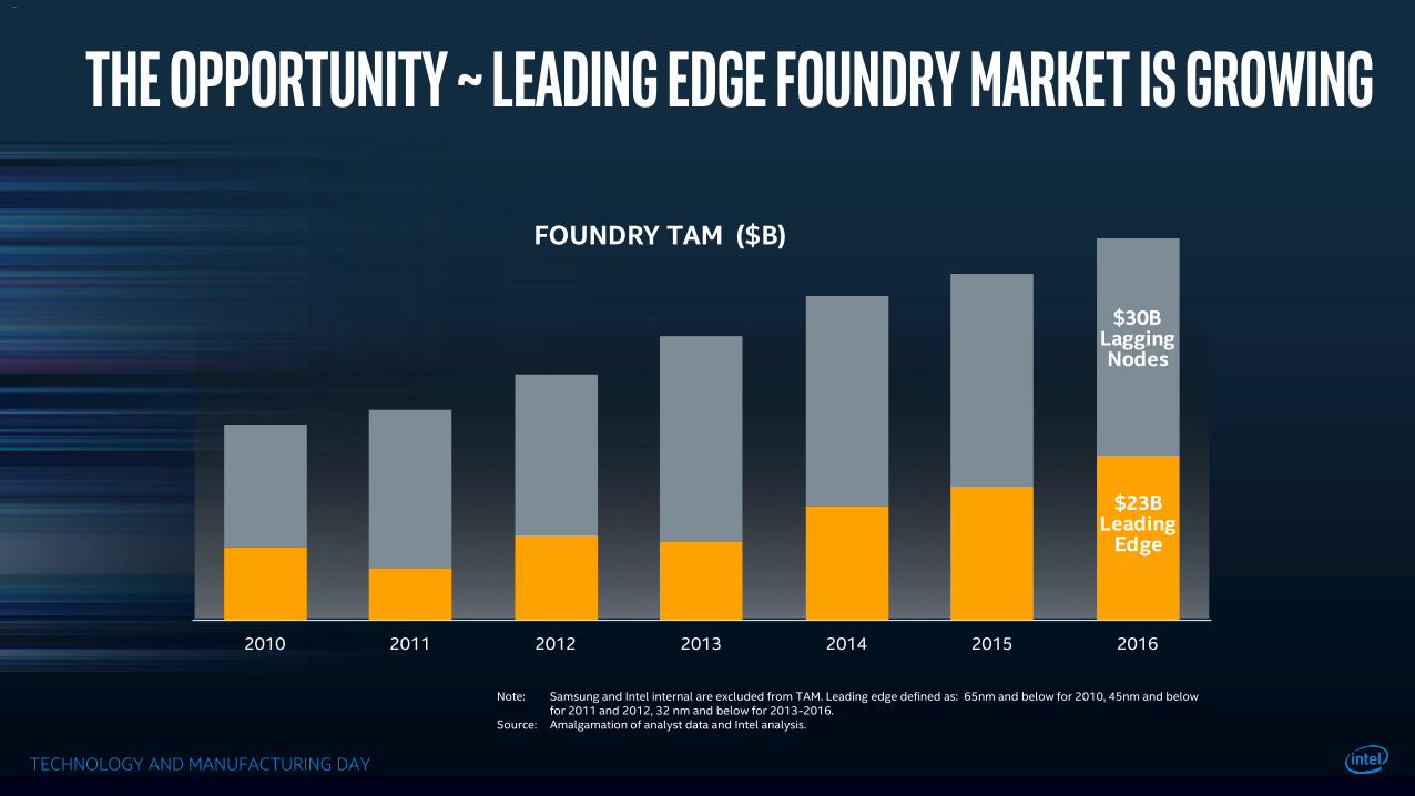
The opportunity ~ Leading edge foundry market is Growing57_84
Note: Samsung and Intel internal are excluded from TAM. Leading edge defined as: 65nm and below for 2010, 45nm and below for 2011 and 2012, 32 nm and below for 2013-2016.
Source: Amalgamation of analyst data and Intel analysis.
FOUNDRY TAM ($B)
2010 2011 2012 2013 2014 2015 2016
$23BLeading
Edge
$30BLaggingNodes

TECHNOLOGY AND MANUFACTURING DAY
2016 Leading Edge Foundry MarketLEADING EDGE
FOUNDRY TAM BY NODE
$23BGROWING AT 14%
(CAGR 2010 - 2016)
2016 TAM ($B)
Note: Samsung and Intel internal are excluded from TAM. Leading edge defined as: 28 nm and below for 2016.Source: Amalgamation of analyst data and Intel analysis.

TECHNOLOGY AND MANUFACTURING DAY
Putting It All TogetherWe continue to advance Moore’s Law
resulting in significant product and cost benefits
Our scale is a unique competitive advantage
We are building a foundry franchise
We continue to outpace the rest of the industry(~3 year lead on 14nm)
TECHNOLOGY AND MANUFACTURING DAY
One More Thing...

TECHNOLOGY AND MANUFACTURING DAY
Presenting 10nm